an Achieving High Accuracy Voltage Regulation DCM
15
AN:035 Page 1 Introduction The DC-DC Converter Module (DCM™) provides isolation, regulation, fault protection and monitoring in a single module. Through a negative slope load line and temperature coefficient, DCM arrays implement wireless current sharing. In either single DCM circuits or in arrays, the nominal load regulation is about 5% (see the %V OUT-LOAD specification in the DCM data sheet), excluding other regulation error terms. This may not be sufficient for applications that have tight voltage regulation requirements. In those applications, an isolated analog feedback loop, such as the one shown in Figure 1, can be used to improve the load regulation performance. The circuit shown here is recommended for general use in high-accuracy applications that need to preserve the input-output isolation offered by the DCM. The circuit is applicable to single DCMs as well as arrays of up to eight units. For array applications, on the primary side, after any needed differential-mode filtering, the DCMs must share a common –IN node, which is also the ground reference for the remote-sense subcircuit output. The DCM TR pins are all driven by single output of the remote-sense subcircuit, so it is important to minimize voltage differences between the various DCM –IN pins through careful layout techniques. On the secondary side, the remote-sense subcircuit senses the output voltage through the R1/R2 resistor network, compares that to a reference voltage, and converts the error voltage into a trim voltage for the whole array. Since the DCMs are all effectively programmed to the same trim voltage, the current sharing between modules is still the same as it would be without the remote-sense circuit, as covered in AN030: Parallel DCMs. This circuit works with all ChiP™ DCM types, and achieves a regulation accuracy of ±1% at all line, load, temperature and trim conditions. Introduction 1 Circuit Schematic 2 Functional Description of Remote-Sense Circuit 3 Component Selection 5 Loop Compensation 6 Experimental Results (Steady State, Start Up, and Transient) 8 Steady-State Load Regulation 8 Start Up 9 Load Transient Response 9 Conclusion 10 Appendix I. Choosing R6 to Account for CTR Variance in the CNY17-3 Over Temperature and Time 11 Appendix II. Current Regulation 12 Contents Page Achieving High-Accuracy Voltage (or Current) Regulation with the DCM Up to ±1% Regulation APPLICATION NOTE | AN:035 Xiaoyan Yu Applications Engineering
Transcript of an Achieving High Accuracy Voltage Regulation DCM
AN:035 Page 1
Introduction
The DC-DC Converter Module (DCM™) provides isolation, regulation, fault protection and monitoring in a single module. Through a negative slope load line and temperature coefficient, DCM arrays implement wireless current sharing. In either single DCM circuits or in arrays, the nominal load regulation is about 5% (see the %VOUT-LOAD specification in the DCM data sheet), excluding other regulation error terms. This may not be sufficient for applications that have tight voltage regulation requirements. In those applications, an isolated analog feedback loop, such as the one shown in Figure 1, can be used to improve the load regulation performance. The circuit shown here is recommended for general use in high-accuracy applications that need to preserve the input-output isolation offered by the DCM. The circuit is applicable to single DCMs as well as arrays of up to eight units.
For array applications, on the primary side, after any needed differential-mode filtering, the DCMs must share a common –IN node, which is also the ground reference for the remote-sense subcircuit output. The DCM TR pins are all driven by single output of the remote-sense subcircuit, so it is important to minimize voltage differences between the various DCM –IN pins through careful layout techniques. On the secondary side, the remote-sense subcircuit senses the output voltage through the R1/R2 resistor network, compares that to a reference voltage, and converts the error voltage into a trim voltage for the whole array.
Since the DCMs are all effectively programmed to the same trim voltage, the current sharing between modules is still the same as it would be without the remote-sense circuit, as covered in AN030: Parallel DCMs.
This circuit works with all ChiP™ DCM types, and achieves a regulation accuracy of ±1% at all line, load, temperature and trim conditions.
Introduction 1
Circuit Schematic 2
Functional Description of Remote-Sense Circuit 3
Component Selection 5
Loop Compensation 6
Experimental Results (Steady State, Start Up, and Transient) 8
Steady-State Load Regulation 8
Start Up 9
Load Transient Response 9
Conclusion 10
Appendix I. Choosing R6 to Account for CTR Variance in the CNY17-3 Over Temperature and Time 11
Appendix II. Current Regulation 12
Contents Page
Achieving High-Accuracy Voltage (or Current) Regulation with the DCM Up to ±1% Regulation
APPLICATION NOTE | AN:035
Xiaoyan YuApplications Engineering

AN:035 Page 2
+IN
-IN
+OUT
-OUT
TR
EN
FT
+IN +OUT
-IN -OUT
TR
EN
FT
+IN +OUT
-IN -OUT
TR
EN
FT
+IN +OUT
-IN -OUT
Module 1
≈≈ ≈≈
Module 2
Module N
PRI-GND SEC-GNDEMI-GND
Remote sense circuit
R6
R7
U3
VTR
C51nF
1
24
5
MAX4238400Ω
CNY17-3
R2
R1
U2
VO VIN GND
C2VREF
U1
2.2uF
10uF
2
31
2
3
4
5 6ADR361
R3C1
R82CC4220AA70J
5VFILT
VEAO
VO VIN
GNDGND
1 87
6
U4LM2936HVMAX-5.0*
1kΩ R8
C6/C7/C8C2012X6S1H475
L1LQH32CN330 5V
0.1uFC9
PRI-SGND SEC-SGND
42.5V
VOUT
RTRIM_1
RTRIM_2
RTRIM_N
≈
(120 kΩ/N) – (R1||R2)
10kΩ
(VOUT -2.5)*R2/2.5
Figure 1
Remote-sense circuit for DCM™
Circuit Schematic
*See Table 1

AN:035 Page 3
Functional Description of Remote-Sense Circuit
The output voltage is sensed through resistor network R1 and R2 relative to secondary ground SEC-SGND; the sensed voltage becomes
1. The sensed voltage is compared to the reference voltage VREF, which in this schematic is generated by the 2.5V reference U1.
If another VREF voltage is preferred, VREF is recommended to be between 1.5V and 3V for optimum noise immunity.
2. The difference gets accumulated by an integrating error amplifier (consisting of R3, C1 and U2), which generates VEAO.
3. The difference between VEAO and 5 VFILT drives the input of the optocoupler U3.
4. The optocoupler (U3) is used to preserve the galvanic isolation of the DCM array.
5. The output of U3 is its collector current. That current develops a voltage drop across the RTRIM_x and RTRIM-INT_x resistors and establishes the DCM™ trim pin voltages. (The RTRIM-INT_x are the internal pull-up resistors inside each DCM. Each RTRIM-INT_x pulls up to VCC, the DCM’s internally generated 3.3V supply.) Figure 2 details how the trim pin voltages are generated, along with a simplified model for N DCMs in parallel. The RTRIM_x resistors are all the same nominal value, as are all of the RTRIM-INT_x resistors.
6. If the sensed version of VOUT is less than VREF, the error amplifier output rises, and the drive current into the optocoupler’s LED is reduced. This in turn reduces the optocoupler’s (output) collector current, permitting the pull-up resistors to pull the trim voltage higher, which raises each DCMs programmed output trim voltage. Conversely, if VOUT is too high, the DCM trim pin voltages are similarly driven lower, which lowers VOUT.
VOUT • (1)R2R1 + R2
VREF = 2.5V (2)
3.3VRTRIM-INT_N
3.3VRTRIM-INT_2
RTRIM_1
RTRIM_2
RTRIM_N
DCM1
DCM2
DCMN
VTR
3.3VRTRIM-INT_1
3.3VRTRIM-INT_x / NRTRIM_x/N
VTR
VTR’_1
VTR’_2
VTR’_N
VTR’
R6
R7
U3VTR
C5
1
24
5
Optocoupler
5VFILTVTR
R6
R7
VTR
C5
1
24
5
Optocoupler
5VFILT
U3
VEAO VEAO
PRI-SGND
Figure 2
Trim voltage generation method
and its simplified model
AN:035 Page 4
7. R6 is chosen to set the voltage transfer ratio of the optocoupler, to ensure that it operates as expected over temperature and with age (see Appendix I).
8. R7 establishes a minimum load on the TR pins by setting the maximum trimbus voltage.
a. R7 must be chosen so that the maximum trim voltage will be below the TR trim enable threshold, even with no optocoupler current; some margin is needed so that trim remains enabled in the presence of noise.
b. The value of R7 may be further reduced, to limit the maximum trim voltage, which can be helpful in reducing overshoot during load transients and start up. For N DCMs in parallel, the trim voltage input to the DCM™, VTR’_x (see Figure 2), can be calculated as:
Where RTRIM_x = 301Ω, RTRIM-INT_x = 10kΩ as specified in the DCM data sheet, N is the number of DCMs in parallel.
Thus the maximum trim voltage input can be calculated as:
For example, if the trim voltage is to be limited to 3V, the value of R7 can be chosen as:
C5 is a low-value ceramic capacitor, such as 1nF, which is used to exclude high-frequency noise from VTR.
9. The bus that is used to supply U1, U2 and U3 is generated from VOUT. Through this method, no external 5V power supply is needed. U4 regulates VOUT to an unfiltered 5V, which is called 5V in Figure 1. This 5V then goes through the filter network (C2, L1, C6-C8) and becomes a filtered 5V, which is called 5VFILT. R8 discharges the filter capacitors when VOUT is off. The output of this circuit is the 5VFILT bus that supplies U1, U2 and U3.
10. Optionally, U4/C6-C8/L1/C2/R8 can be removed from the circuit if a precision external 5V power supply with at least 50mA capability is available to drive the 5VFILT bus. The benefit of using an external 5V power supply is that it uses fewer components. The disadvantage is that if the external supply is energized before the DCMs are enabled, then the error amplifier will “wind up” to a maximum trim condition. When the DCMs are started, the system output voltage will significantly overshoot the setpoint until the integrator unwinds. When using an external 5V power supply, R7 should be chosen carefully so that VOUT does not exceed the maximum voltage allowed by the application, or the DCMs should be enabled prior to energizing the external 5V supply node.
(3)VTR’max = 3.3 • N • R7 + RTRIM_x
N • R7 + RTRIM_x + RTRIM-INT_x(3)VTR’max = 3.3 •
N • R7 + RTRIM_x
N • R7 + RTRIM_x + RTRIM-INT_x
VTR’max = 3.3 • (4)N • R7 + 301N • R7 + 10301VTR’max = 3.3 • (4)N • R7 + 301
N • R7 + 10301
R7 = (5)100kΩNR7 = (5)100kΩ
N

AN:035 Page 5
Through this method, the output voltage of the DCM™ can be trimmed to:
The maximum cut off frequency of the whole loop is 30Hz, but with CTR variance, temperature, and aging of the optocoupler, it can be as low as approximately 7.5Hz.
Component Selection
The following resources can be used to facilitate the selection of filter network components:
n Each DCM’s data sheet
n AN030: Parallel DCMs
n Powerbench Filter Design Tool
n AN023: Filter Network Design for DC-DC Converter Modules
The detailed schematic of the DCM remote-sense circuit has been shown in Figure 1, with IC device types and component values. The generic components’ part numbers have not been marked in the schematic. Unconnected pins have not been shown for simplicity.
VOUT = VREF • (6)R1 + R2R2
Table 1
Notes for the choice of U4VOUT U4 Recommendation Comment
6V ≤ VOUT ≤ 60V Use LM2936HVMAX-5.0 for U4
VOUT ≤ 6V
Use an appropriate regulator for U4 so that the output voltage of U4 will be between 4V and 5.5V, or use an independent supply rail in the application
For DCM modules with a rated VOUT-NOM of 5V or 3.3V, for example.
AN:035 Page 6
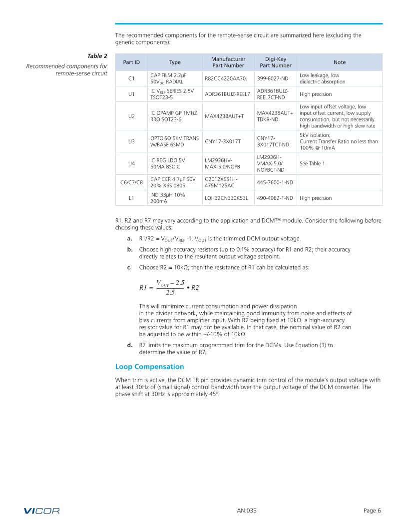
The recommended components for the remote-sense circuit are summarized here (excluding the generic components):
R1, R2 and R7 may vary according to the application and DCM™ module. Consider the following before choosing these values:
a. R1/R2 = VOUT/VREF -1, VOUT is the trimmed DCM output voltage.
b. Choose high-accuracy resistors (up to 0.1% accuracy) for R1 and R2; their accuracy directly relates to the resultant output voltage setpoint.
c. Choose R2 = 10kΩ; then the resistance of R1 can be calculated as:
This will minimize current consumption and power dissipation in the divider network, while maintaining good immunity from noise and effects of bias currents from amplifier input. With R2 being fixed at 10kΩ, a high-accuracy resistor value for R1 may not be available. In that case, the nominal value of R2 can be adjusted to be within +/-10% of 10kΩ.
d. R7 limits the maximum programmed trim for the DCMs. Use Equation (3) to determine the value of R7.
Loop Compensation
When trim is active, the DCM TR pin provides dynamic trim control of the module’s output voltage with at least 30Hz of (small signal) control bandwidth over the output voltage of the DCM converter. The phase shift at 30Hz is approximately 45°.
Table 2
Recommended components for remote-sense circuit
R1 = • R2VOUT – 2.5
2.5
Part ID TypeManufacturer Part Number
Digi-Key Part Number
Note
C1CAP FILM 2.2µF 50VDC RADIAL
R82CC4220AA70J 399-6027-NDLow leakage, low dielectric absorption
U1IC VREF SERIES 2.5V TSOT23-5
ADR361BUJZ-REEL7ADR361BUJZ-REEL7CT-ND
High precision
U2IC OPAMP GP 1MHZ RRO SOT23-6
MAX4238AUT+TMAX4238AUT+TDKR-ND
Low input offset voltage, low input offset current, low supply consumption, but not necessarily high bandwidth or high slew rate
U3OPTOISO 5KV TRANS W/BASE 6SMD
CNY17-3X017TCNY17-3X017TCT-ND
5kV isolation; Current Transfer Ratio no less than 100% @ 10mA
U4IC REG LDO 5V 50MA 8SOIC
LM2936HV-MAX-5.0/NOPB
LM2936H-VMAX-5.0/NOPBCT-ND
See Table 1
C6/C7/C8CAP CER 4.7µF 50V 20% X6S 0805
C2012X6S1H-475M125AC
445-7600-1-ND
L1IND 33µH 10% 200mA
LQH32CN330K53L 490-4062-1-ND High precision

AN:035 Page 7
The whole open loop transfer function at 30Hz or below can be calculated as:
Where CTR is the Current Transfer Ratio of the optocoupler, which is specified in the optocoupler data sheet;
recall that N is the number of DCM™ modules in parallel.
For frequencies less than or equal to 30Hz, the analysis is as follows:
ATR (s) is the transfer function from TR to VOUT, which is a constant ATR at very low frequency and ≤ATR at 30Hz.
Rearranging the equality:
Multiplying both sides by ATR (s),
The term increases with increasing trim range. For existing DCMs, the
widest trim range is −40% to 10% of VOUT_NOM. For these DCMs,
Therefore:
Inserting this result into Equation 7:
If R3 is chosen so that A(s) goes to 0dB at 30Hz, the whole system will have approximately 45° phase margin.
A(s) = ATR(s) • • CTR •• (7)R2R2 + R1
RTRIM-INT_x
N • R61
R3’ • C1 • s
R3’ = R3 + R1 • R2R1 + R2
VOUT • (8)= 2.5R2R1 + R2
= (9)R2R2 + R1
2.5VOUT
ATR(s) • = (10)R2R2 + R1
2.5 • ATR(s)VOUT
2.5 • ATR(s)VOUT
12.5 • ATR
VOUT_MIN
ATR(s) • ≤ 1 (11)R2R2 + R1
A(s) ≤ 1 • • CTR • (12)1R3’ • 2.2µF • s
10kΩN • 400

AN:035 Page 8
Setting A(s) to 0dB at 30Hz results in:
For the optocoupler used in the schematic, the maximum CTR is in the range of 1 to 2. So for the worst case gain, CTR = 2:
Experimental Results (Steady State, Start Up, and Transient)
Steady State Load Regulation
Using the DCM4623TD2H53E0T00 as an example, experimental results for a single DCM™ are shown in Figure 3; the results for an array of eight DCMs are shown in Figure 4.
R3’ = (13)60kΩ • CTR
N
(14)R3’ = 120kΩN
(15)R3 = –120kΩN
R1 • R2R1 + R2
V OU
T Reg
ulat
ion
Erro
r (%
)
Rated Load (%)
Low Line Nom LineHigh Line
Low Trim
-0.25
-0.15
-0.05
0.05
0.15
0.25
0 20 40 60 80 100
V OU
T Reg
ulat
ion
Erro
r (%
)
Rated Load (%)
Low Line Nom LineHigh Line
Low Trim
-0.25
-0.15
-0.05
0.05
0.15
0.25
0 20 40 60 80 100
Figure 3
The experimental results for single DCM4623TD2H53E0T00
with this remote-sense circuit
Figure 4
Experimental results for an 8-up DCM4623TD2H53E0T00 array with this remote-sense circuit
V OU
T Reg
ulat
ion
Erro
r (%
)
Rated Load (%)
Low Line Nom LineHigh Line
High Trim
-0.25
-0.15
-0.05
0.05
0.15
0.25
0 20 40 60 80 100
V OU
T Reg
ulat
ion
Erro
r (%
)
Rated Load (%)
Low Line Nom LineHigh Line
High Trim
-0.25
-0.15
-0.05
0.05
0.15
0.25
0 20 40 60 80 100

AN:035 Page 9
Start Up
Typical start-up waveforms are shown in Figure 5 and Figure 6. During start up, once VOUT reaches U4’s minimum input voltage, U4 will generate the 5V bus to supply U1, U2 and U3. The waveform of the start up typically comes in two stages: in the first stage, VOUT rises to the minimum trimmed VOUT; in the second stage, the circuit comes to the steady state and brings VOUT to the correct trimmed value.
This circuit needs to be started up after VOUT and the 5V bus have fully discharged to avoid trimming to the highest VOUT.
Load Transient Response
There is a delay from the transient until the circuit reaches the corrected output voltage, which is due to the limited bandwidth of the DCM TR pin and remote-sense circuit. Because of this narrow bandwidth, the remote-sense circuit doesn’t affect the initial response to a transient. Figure 7 shows a comparison of transient response without the remote-sense circuit to the response with the remote-sense circuit in operation.
Figure 5
Experimental results for a single DCM4623TD2H53E0T00 (low line, maximum external COUT)
start up into high trim with this remote-sense circuit
Figure 6
Experimental results for a single DCM4623TD2H53E0T00 (high line, maximum external COUT)
start up into low trim with this remote-sense circuit
(a) 10% load
(a) 10% load
(b) Full load (electronics load in CR mode)
(b) Full load (electronics load in CR mode)

AN:035 Page 10
Figure 7
Comparison of a single DCM4623TD2H53E0T00
transient response (nominal line, nominal trim, electronic
load in CC mode 10% to 100% load transient) without the
remote-sense circuit and with the circuit included
Conclusion
Using the remote-sense circuit shown here, DCM-based voltage regulators can achieve output voltage accuracy of ±1%. Within the 30Hz bandwidth of the circuit, other aspects of DCM™ operation are unchanged. This method works for any number of DCMs in parallel, up to eight.
(a) Without remote-sense circuit (b) With remote-sense circuit

AN:035 Page 11
Appendix I. Choosing R6 to Account for CTR Variance in the CNY17-3 Over Temperature and Time
1. Information from Vishay CNY17 data sheet
2. Calculation of CNY17-3 controller current achievable over temperature and time:
nChoosing R6 = 400Ω, a supply voltage of 4V (the lowest value specified in Table 1), CTR = 100% and estimating the voltage drop across the optocoupler at 1.28V, the maximum forward current that the secondary side of the remote-sense circuit could have over the full temperature range is approximately (4V − 1.28V)/400Ω = 6.8mA.
n The next step is to find the minimum CTR at IF = 6.8mA, using linear interpolation on the data in the table for IF = 1mA and IF = 10mA. This results in a minimum CTR of ((10mA − 6.8mA) • 34% + (6.8mA − 1mA) • 100%)/(10mA – 1mA) = 76.5% at 25ºC
n From the Normalized CTR curves above, CTR could decrease to 60% of its peak value over temperature, which is 76.5% • 60% = 45.9%
n From Vishay reliability data, CTR is reduced by 15% over 8000 operation hours, giving CTR = 45.9% • (1 − 15%) = 39%
n Thus the collector current will be at least 6.8mA • 39% = 2.65mA, to ensure proper operation with aging.
n Since 3.3V – (2.65V • 1.25) = −0.01V < 0V, this will result in a trim voltage close to 0V, which is sufficient to drive all DCMs to trim low.
n When the forward current is small, the CNY17-3 will be able to drive all DCMs to high trim, so high trim is achievable for any choice of R6.
Thus R6 = 400Ω should be a valid choice for this circuit to work over temperature and time, from single DCMs through arrays of eight DCMs.
Fig. 5 - Forward Voltage vs. Forward Current
0.6
0.80.91.01.11.21.31.4
1.8
0.1 1 10 100IF - Forward Current (mA)
V F -
Forw
ard
Volta
ge (V
)
Tamb = - 55 °C
1.5
0.7
Tamb = - 25 °C
Tamb = 110 °C
1.61.7
Tamb = 0 °C
Tamb = 25 °C
Tamb = 50 °C
Tamb = 75 °CTamb = 100 °C
CURRENT TRANSFER RATIO (Tamb = 25 °C, unless otherwise specified)PARAMETER TEST CONDITION PART SYMBOL MIN. TYP. MAX. UNIT
IC/IF
VCE = 5 V, IF = 10 mA
CNY17-1 CTR 40 80 %CNY17-2 CTR 63 125 %CNY17-3 CTR 100 200 %CNY17-4 CTR 160 320 %
VCE = 5 V, IF = 1 mA
CNY17-1 CTR 13 30 %CNY17-2 CTR 22 45 %CNY17-3 CTR 34 70 %CNY17-4 CTR 56 90 %
Fig. 11 - Normalized CTR (NS) vs. Forward Current Fig. 12 - Normalized CTR (sat) vs. Forward Current
0
0.2
0.6
0.4
0.8
1.0
1.2
0011.0IF - Forward Current (mA)
CTR
Nor
m -
Nor
mal
ized
CTR
(NS)
1 10
Tamb = - 55 °C
Tamb = - 40 °C
Tamb = 0 °CTamb = 25 °C
Tamb = 50 °CTamb = 75 °C
Tamb = 110 °C
VCE = 5 V
Tamb = 100 °C
IF = 10 mA
0
0.2
0.6
0.4
0.8
1.0
1.2
0011.0IF - Forward Current (mA)
CTR
Nor
m -
Nor
mal
ized
CTR
(sat
)
1 10
Tamb = - 55 °C
Tamb = - 40 °CTamb = 0 °C
Tamb = 25 °C
Tamb = 50 °C
Tamb = 75 °C
Tamb = 110 °C
VCE = 0.4 V
Tamb = 100 °C
IF = 10 mA
Tables and Figures courtesy of Vishay Intertechnology, Inc.

AN:035 Page 12
Appendix II. Current Regulation
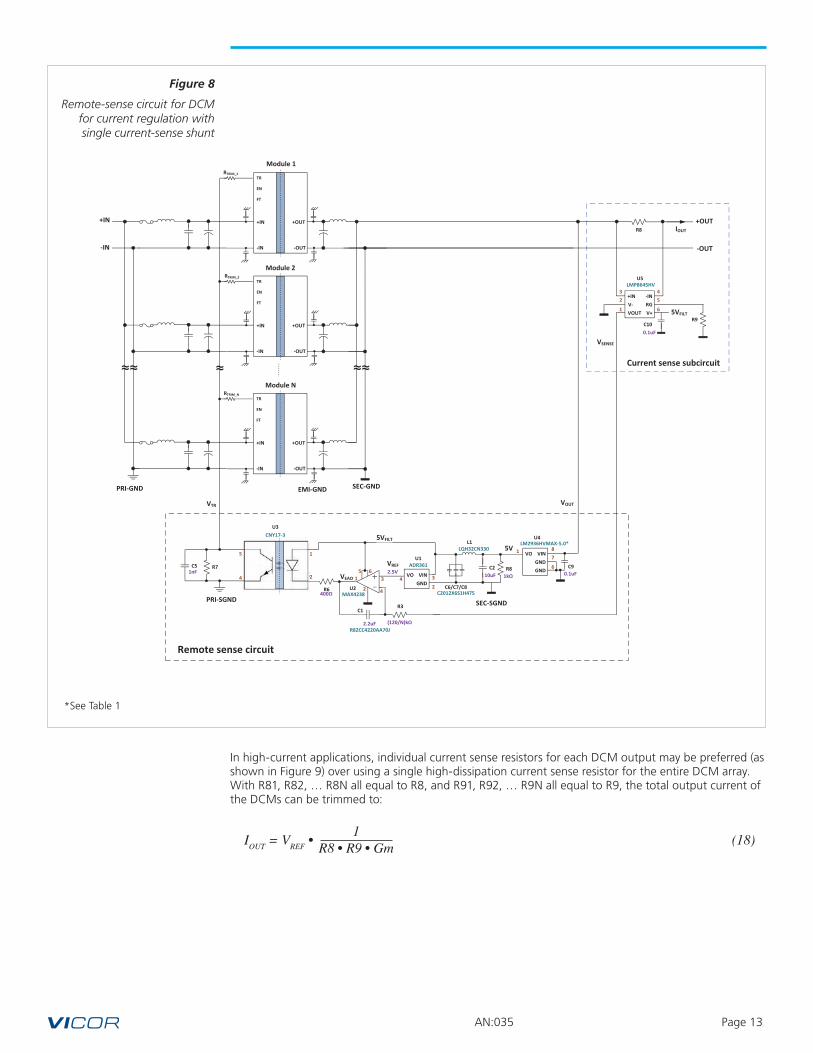
If current regulation is needed instead of voltage regulation, with some modifications, the remote-sense circuit can be adapted to regulate a constant-current output.
Instead of sensing the output voltage with R1 and R2, a shunt resistor is used to measure the output current. The voltage across the shunt resistor is sensed with an additional differential amplifier stage, which feeds R3. R1 and R2 are not present, since the current signal scaling is accomplished by current sense amplifier. The rest of the circuit is unchanged. A typical schematic with the current sense sub-circuit is shown in Figure 8.
Notice that current regulation needs to be limited to the minimum rated output current (IOUT) of the DCM, to avoid interfering with the DCM’s operational current limit and cause issues.
In applications such as battery charging, the actual VOUT can be different from the trimmed voltage of the DCM. Additional considerations may be needed:
1. The DCM has a minimum VOUT before it might detect output under voltage. For example, the DCM would not be able to charge a battery whose voltage is below VOUT_UVP.
2. The DCM current capability is reduced when the DCM is trimmed higher than nominal (regardless of the actual VOUT), so the output current from the system should be no higher than n · (Rated POUT/MAXIMUM VOUT-TRIMMING) to avoid entering current limit.
The transfer function between the output current IOUT and the sense voltage VSENSE in Figure 8 is:
With an LMP8645HV, the typical Gm is 200µA/V.
Through this method, the total output current of the DCMs can be trimmed to:
(16)VSENSE = IOUT • R8 • R9 • Gm
(17)IOUT = VREF • 1R8 • R9 •Gm
AN:035 Page 13
+OUT
-OUT
R8
+IN -INV- RGVOUT V+
45
6
32
1
R9
0.1uFC10
5VFILT
Current sense subcircuit
LMP8645HVU5
IOUT
VSENSE
+IN
-IN
TR
EN
FT
+IN +OUT
-IN -OUT
TR
EN
FT
+IN +OUT
-IN -OUT
TR
EN
FT
+IN +OUT
-IN -OUT
Module 1
≈≈ ≈≈
Module 2
Module N
PRI-GND SEC-GNDEMI-GND
Remote sense circuit
R6
R7
U3
VTR
C51nF
1
24
5
MAX4238400Ω
CNY17-3
U2
VO VIN GND
C2VREF
U1
2.2uF
10uF
(120/N)kΩ
2
31
2
3
4
5 6ADR361
R3C1
R82CC4220AA70J
5VFILT
VEAO
VO VINGNDGND
1 87
6
U4LM2936HVMAX-5.0*
1kΩ R8
C6/C7/C8C2012X6S1H475
L1LQH32CN330 5V
0.1uFC9
PRI-SGND SEC-SGND
42.5V
VOUT
RTRIM_1
RTRIM_2
RTRIM_N
≈
Figure 8
Remote-sense circuit for DCM for current regulation with single current-sense shunt
(18)IOUT = VREF • 1R8 • R9 •Gm
*See Table 1
In high-current applications, individual current sense resistors for each DCM output may be preferred (as shown in Figure 9) over using a single high-dissipation current sense resistor for the entire DCM array. With R81, R82, … R8N all equal to R8, and R91, R92, … R9N all equal to R9, the total output current of the DCMs can be trimmed to:

AN:035 Page 14
+OUT
-OUT
+IN
-IN
TR
EN
FT
+IN +OUT
-IN -OUT
TR
EN
FT
+IN +OUT
-IN -OUT
TR
EN
FT
+IN +OUT
-IN -OUT
Module 1
≈≈ ≈≈
Module 2
Module N
(120/N)kΩ R31
PRI-GND SEC-GNDEMI-GND
R81
+IN -INV- RGVOUT V+
45
6
32
1
R91
0.1uFC101
5VFILT
LMP8645HVU51
IOUT_1
VSENSE_1
R82
+IN -INV- RGVOUT V+
45
6
32
1
R92
0.1uFC102
5VFILT
LMP8645HVU52
IOUT_2
VSENSE_2
R8N
+IN -INV- RGVOUT V+
45
6
32
1
R9N
0.1uFC101
5VFILT
LMP8645HVU5N
IOUT_N
VSENSE_N
(120/N)kΩ R32
(120/N)kΩ R3N
Current sense subcircuit
Remote sense circuit
R6
R7
U3
VTR
C51nF
1
24
5
MAX4238400Ω
CNY17-3
U2
VO VIN GND
C2VREF
U1
2.2uF
10uF
2
31
2
3
4
5 6ADR361
C1
R82CC4220AA70J
5VFILT
VEAO
VO VINGNDGND
1 87
6
U4LM2936HVMAX-5.0*
1kΩ R8
C6/C7/C8C2012X6S1H475
L1LQH32CN330 5V
0.1uFC9
PRI-SGND SEC-SGND
42.5V
VOUT
RTRIM_1
RTRIM_2
RTRIM_N
≈
Figure 9
Remote-sense circuit for DCM for current regulation with
individual current-sense shunts
*See Table 1

Contact Us: http://www.vicorpower.com/contact-us
Vicor Corporation25 Frontage Road
Andover, MA, USA 01810Tel: 800-735-6200Fax: 978-475-6715
www.vicorpower.com
emailCustomer Service: [email protected]
Technical Support: [email protected]
©2017 – 2019 Vicor Corporation. All rights reserved. The Vicor name is a registered trademark of Vicor Corporation.All other trademarks, product names, logos and brands are property of their respective owners.
Limitation of WarrantiesInformation in this document is believed to be accurate and reliable. HOWEVER, THIS INFORMATION IS PROVIDED “AS IS” AND WITHOUT ANY WARRANTIES, EXPRESSED OR IMPLIED, AS TO THE ACCURACY OR COMPLETENESS OF SUCH INFORMATION. VICOR SHALL HAVE NO LIABILITY FOR THE CONSEQUENCES OF USE OF SUCH INFORMATION. IN NO EVENT SHALL VICOR BE LIABLE FOR ANY INDIRECT, INCIDENTAL, PUNITIVE, SPECIAL OR CONSEQUENTIAL DAMAGES (INCLUDING, WITHOUT LIMITATION, LOST PROFITS OR SAVINGS, BUSINESS INTERRUPTION, COSTS RELATED TO THE REMOVAL OR REPLACEMENT OF ANY PRODUCTS OR REWORK CHARGES).
Vicor reserves the right to make changes to information published in this document, at any time and without notice. You should verify that this document and information is current. This document supersedes and replaces all prior versions of this publication.
All guidance and content herein are for illustrative purposes only. Vicor makes no representation or warranty that the products and/or services described herein will be suitable for the specified use without further testing or modification. You are responsible for the design and operation of your applications and products using Vicor products, and Vicor accepts no liability for any assistance with applications or customer product design. It is your sole responsibility to determine whether the Vicor product is suitable and fit for your applications and products, and to implement adequate design, testing and operating safeguards for your planned application(s) and use(s).
VICOR PRODUCTS ARE NOT DESIGNED, AUTHORIZED OR WARRANTED FOR USE IN LIFE SUPPORT, LIFE-CRITICAL OR SAFETY-CRITICAL SYSTEMS OR EQUIPMENT. VICOR PRODUCTS ARE NOT CERTIFIED TO MEET ISO 13485 FOR USE IN MEDICAL EQUIPMENT NOR ISO/TS16949 FOR USE IN AUTOMOTIVE APPLICATIONS OR OTHER SIMILAR MEDICAL AND AUTOMOTIVE STANDARDS. VICOR DISCLAIMS ANY AND ALL LIABILITY FOR INCLUSION AND/OR USE OF VICOR PRODUCTS IN SUCH EQUIPMENT OR APPLICATIONS AND THEREFORE SUCH INCLUSION AND/OR USE IS AT YOUR OWN RISK.
Terms of SaleThe purchase and sale of Vicor products is subject to the Vicor Corporation Terms and Conditions of Sale which are available at: (http://www.vicorpower.com/termsconditionswarranty)
Export ControlThis document as well as the item(s) described herein may be subject to export control regulations. Export may require a prior authorization from U.S. export authorities.
08/19 Rev 1.4 Page 15