AN ABSTRACT OF THE THESIS OF - CORE · AN ABSTRACT OF THE THESIS OF ... power DC-DC converter...
70
Transcript of AN ABSTRACT OF THE THESIS OF - CORE · AN ABSTRACT OF THE THESIS OF ... power DC-DC converter...

AN ABSTRACT OF THE THESIS OF
Brian A. Miller for the degree of Master of Science in
Electrical and Computer Engineering presented on February 27, 2013
Title: A DC-DC Converter Architecture for Low-Power, High-Resistance
Thermoelectric Generators for use in Body-Powered Designs
Abstract approved:
Terri S. Fiez Kartikeya Mayaram
This thesis presents a low power DC-DC converter suitable for harvesting energy
from high impedance thermoelectric generators (TEGs) for the use in body powered
electronics. The chip has been fabricated in a 130nm CMOS technology. To meet the
power demands of body powered networks, a novel dual-path architecture capable of
efficiently harvesting power at levels below 5 μW has been developed. To control the
converter, a low power control loop has been developed. The control loop features a
low-power clock and a pulse counting system that is capable of matching the converter
impedance with high impedance TEGs. The system consumes less than 900nW of
quiescent power and maintains an efficiency of 68% for a load of 5 μW.

©Copyright by Brian A. Miller
February 27, 2013
All Rights Reserved
A DC-DC Converter Architecture for Low-Power, High-Resistance
Thermoelectric Generators for use in Body-Powered Designs
by
Brian A. Miller
A THESIS
Submitted to
Oregon State University
in partial fulfillment of
the requirements for the
degree of
Master of Science
Presented February 27, 2013
Commencement June 2013

Master of Science thesis of Brian A. Miller presented on February 27, 2013.
APPROVED:
Co-Major Professor, representing Electrical and Computer Engineering
Co-Major Professor, representing Electrical and Computer Engineering
Director of the School of Electrical Engineering and Computer Science
Dean of the Graduate School
I understand that my thesis will become part of the permanent collection of Oregon State
University libraries. My signature below authorizes release of my thesis to any reader
upon request.
Brian A. Miller, Author

ACKNOWLEDGEMENTS
First I would like to thank my major professors Dr. Terri Fiez and Dr. Kartikeya
Mayaram, for supporting my work and always pushing me to achieve more. It may not
have always been smooth sailing and I admittedly pushed back a lot, but there is no doubt
that I am a better engineer and an all-around more driven person as a result. I would also
like to thank my committee members for their time and support despite what I am sure
are very busy schedules.
I would like to thank all of the professors I have had in my seven and a half years
at Oregon State University. Even though there is not enough room to list every professor
I have had, they have all made an impact. I especially would like to thank Roger Traylor.
I may have only been in two of his classes, but they were the two most important courses
I ever took in terms of growing as an engineer, and recognizing the things that are
possible with a little hard work. I would also like to thank Dr. Gabor Temes who I was
fortunate enough to take three courses with in grad-school. I will always remember the
jokes he told in class as well as be amazed that an individual so accomplished, can also
be so modest.
To my group mates Siladitya Dey, Justin Goins, Ankur Guha Roy, Hamid
Maghami, Hossein Mirzaie, Mohsen Nasroullahi, Ronghua Ni, Saeed Pourbagheri,
Saurahb Saxena, Samira Zaliasl, and Ramin Zanbaghi; thanks for the help over the past
two and half years of grad-school I cannot give enough thanks. Special thanks to Justin
and Ankur. I do not even want to think about how much of your time I have wasted over

the past two and a half years. I’m sure you’d have your PhD’s by now without me .
Alas I am leaving and I’m sure your productivity will increase. For Justin, I’m sure I will
never see you again(At least I hope it works out the same way as the last time I said that.)
To my friends who have always supported me I offer the largest thanks
imaginable. There are too many people to list, but a special thanks to Kellen Arb,
Dominique Be, Taylor Dark, Ian Rose, and Tonya Sartor. I’m sure none of you will ever
read this, but if you do find yourself in that unfortunate position, you have all been a
tremendous help in allowing me to reach where I am today.
Finally I would like to thank my family. To my father you have always been a
great source of knowledge. It is always nice to have somebody who traveled the same
path before who can offer guidance. To my mother I thank you for being there
throughout all the late and panicked phone calls. Thanks to my older sister Casey for
helping edit my thesis and offering legal advice for all my crazy shenanigans. To Erik
who while admittedly a pain at times was a great help to me while I too pursued a masters
degree in engineering at Oregon State. To my younger siblings Andrew and Annalise, it
is exciting to see you two pursuing your own engineering degrees. You are two of the
most capable people I know and the sky is the limit. Things may get rough at times, but
with hard work and dedication light will always shine through in the end.
I apologize for those who have not been listed. It would take another 20 pages to
give thanks to all those who are deserving. For everybody not listed, I thank you as well
and can only hope to give back the type of help and support which I have received.

TABLE OF CONTENTS
Page
1. Introduction ................................................................................................................. 1
2. Requirements for body-powered TEG DC-DC converters ......................................... 4
3. Existing DC-DC converter architectures ..................................................................... 6
3.1. The Two-Converter Architecture ......................................................................... 6
3.2. The Single Boost Architecture ............................................................................. 8
3.3. The Dual-Path Architecture ................................................................................. 9
4. Overview of Proposed Architecture .......................................................................... 10
5. Implementation of the Proposed Architecture ........................................................... 12
5.1. Design for impedance match .............................................................................. 15
5.2. Low-power ring oscillator .................................................................................. 18
6. Measurement results .................................................................................................. 23
7. Conclusions ............................................................................................................... 32
Bibliography ..................................................................................................................... 34
Appendices ........................................................................................................................ 37

LIST OF FIGURES
Figure Page
1: Body-powered energy harvesting circuit. ...................................................................... 4
2: DC-DC converter architectures. (a) Two converter architecture.
(b) Single boost architecture. (c) Dual path architecture. .................................................. 8
3: Proposed architecture. .................................................................................................. 12
4: DC-DC converter schematics. (a) Overall schematic. (b) Circuit operating in the
standard mode. (c) Circuit operating in the secondary mode. ......................................... 13
5: Typical current-starved ring oscillator. ........................................................................ 19
6: Single oscillator cell..................................................................................................... 20
7: (a) Oscillator output with single current source on top.
(b) Oscillator output with current source on top and bottom. ........................................... 21
8: Complete current-starved oscillator. ............................................................................ 22
9: Simulated output of oscillator (a) before, and (b) and after added inverter. ................ 23
10: Die photograph of the converter. ............................................................................... 23
11: Clock and pulse-counting signals. ............................................................................. 25
12: Open-circuit TEG voltage and converter input voltage. ............................................ 25
13: Switch gate voltages. ................................................................................................. 27
14: Zoomed in switch gate voltages. ................................................................................ 27
15: Standard mode performance of the converter. ........................................................... 28
16: Transferred power vs. storage node voltage. ............................................................. 31
17: Efficiency of secondary operation vs. storage node voltage. .................................... 32

LIST OF APPENDICIES
Appendix Page
A: Available electrical power from body heat .................................................................. 38
B: Testing Details ............................................................................................................. 41
C: Design considerations for low-power converter operation ......................................... 44
D: Converter signal generation ........................................................................................ 45
E: Circuitry in pulse counting block ................................................................................ 49
F: Flag generation circuitry .............................................................................................. 51
G: Reference Generator ................................................................................................... 54
H: Oscillator Biasing........................................................................................................ 56

LIST OF APPENDIX FIGURES
Figure Page
A - 1: Bonding (a) before soldering, and (b) after soldering. .......................................... 43
A - 2: Circuit for control signal generation. ..................................................................... 46
A - 3: Pulse generation blocks. ........................................................................................ 49
A - 4: 5-bit incrementer.................................................................................................... 50
A - 5: Schematic of 1/32 pulse generation block ............................................................. 50
A - 6: Flag generation blocks. .......................................................................................... 51
A - 7: Simulation of secondary mode. ............................................................................. 53
A - 8: Bias generation circuit ........................................................................................... 54
A - 9: Dependence of VBIAS on Temperature and supply voltage (curved line). Straight
line is Vdd/2. ..................................................................................................................... 55
A - 10: Switched-capacitor divider for oscillator ............................................................ 57
A - 11: Detailed oscillator schematic ............................................................................... 57

DEDICATION
This thesis is dedicated to my parents and four siblings who have stuck with me through
all my years of schooling. Thanks for the support socially, emotionally, and
economically as well as the patience for putting up with me during my seven and a half
years of college. Additional dedications to Dan and Ilo Richmond, and my beloved dog
Benny. You may be gone from this world, but never will you be forgotten.
1. INTRODUCTION
Advances in portable electronics have enabled sensing in applications ranging
from human health to environmental monitoring to structural integrity. The form factor
of these sensing systems continues to shrink due to the scaling of integrated circuits while
the functionality increases. Additionally, power reductions achieved through technology
scaling and energy efficient design techniques also have helped reduce the battery power,
and therefore, the total weight and size of the sensing system. One approach used to
further reduce the size and weight of sensing systems is to scavenge energy from the
environment. This avoids having to replace batteries by extending battery life or
removing the need for batteries altogether [1-7]. Energy can be harvested from a range of
sources and some examples include harvesting radio frequency (RF) radiation to power
RFID tags [8-9], harvesting vibrational energy in train stations and dance floors with
piezoelectric harvesters [10-11], scavenging light with solar cells to power wrist watches
[12] or for large scale energy production [13], and converting waste heat into usable
energy with thermoelectric generators (TEGs) for industrial monitoring [14].
With the advances in energy harvesting, a new area of research is body-powered
electronics which relies on harvesting energy either from the body, or in close proximity
to the body. Techniques that have been used in these applications include piezoelectric
transducers used to harvest energy from walking [1] and TEGs extracting energy from
2
body heat [3] by transforming thermal gradients into electrical power. Since the human
body releases a considerable amount of heat at all times, the use of TEGs in body-
powered electronics has tremendous potential.
A typical TEG consists of two thermally conductive plates that when heated to
different temperatures, create an electrical potential. In body-powered electronics, this
potential is created when one plate is heated by the skin, and the other is cooled by the
ambient air. Since many health monitoring systems already require contact between the
probes and the skin, harvesting energy in this manner is a non-intrusive way to
supplement, or replace batteries.
One shortcoming of TEGs is that the harvestable power is relatively low. With
small TEGs appropriate for body area networks, the power harvested can be as low as 5
μW (Appendix A). Thus, to make a full sensing system that uses this power source
exclusively, the sensor and sensor electronics must be designed for ultra low-power
operation. There are examples of some systems that meet these stringent requirements.
These include temperature sensors consuming less than a microwatt of power [15] and
motion sensors consuming as little as 2.5 microwatts [16]. Some medical devices
consuming less than 1 mW have been demonstrated using body heat as the sole energy
source. However, cumbersome heat sinks, which caused uncomfortable chills for the test
subjects, were required [2, 17].
Reducing the power consumed by the sensors and sensing systems is only part of
the solution. The circuitry that converts the energy harvested to usable power can also
3
result in significant power losses without careful design [3]. Dealing with power levels
on the microwatt scale requires power management circuits that can maintain good
efficiency with very low power levels. Additionally, a key requirement is maximizing
the energy delivered to the load.
Thermal energy harvesting techniques have advanced in recent years, but their
feasibility in body-powered applications is still limited by two main problems. First,
many researchers have assumed power levels of tens of microwatts will be readily
available [3, 18]. For devices currently in development or on the market, this is an
optimistic assumption (Appendix A). Second, while a "good" power source generally has
a low output impedance on the order of a few ohms, in order to get a suitable output
voltage with low power, compact TEGs useful for body area networks have output
impedances in the range of kilo ohms [19-20]. Prior techniques focus solely on low
impedance TEGs since impedance matching is easier with such devices. These systems
require a larger voltage boost making high efficiency harder to obtain. Existing power
management techniques [3, 18] thus are inefficient and impractical for real applications
where harvestable power is low, and the TEG resistance is high.
New power management techniques must be developed in order to operate sensing
systems at power levels below 10 μW and to enable the use of high resistance TEGs. In
this thesis, a low power, DC-DC converter capable of interfacing with high impedance
TEGs is presented and tested. The converter is designed to interface with a TEG
produced by Perpetua Power, featuring an output resistance of 20kΩ. Under a load of
4
5μW, the converter efficiency is nearly 70%. In order to meet the low power demands
while interfacing with high impedance TEGs, a new converter architecture was
developed. In addition, an efficient control system and a low power clock have also been
developed.
This thesis is organized into the following sections. Section 2 describes a typical
TEG harvesting setup and lists requirements for body-powered systems. Section 3
discusses previous converter architectures and presents advantages and disadvantages for
each design. Section 4 provides a brief overview of the new converter architecture, and
Section 5 describes the detailed circuit level implementation. Section 6 presents the
measured results of the new converter and compares the results with previous work.
Finally, Section 7 concludes the paper.
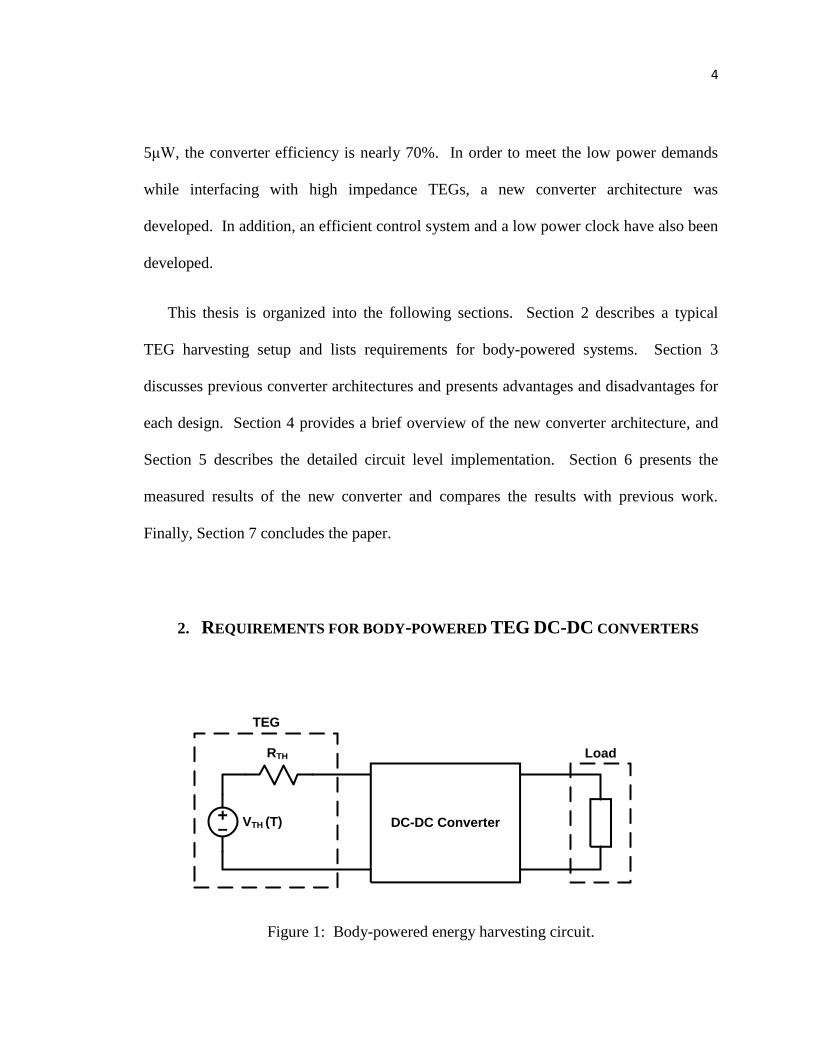
2. REQUIREMENTS FOR BODY-POWERED TEG DC-DC CONVERTERS
VTH (T)
RTH
TEG
Load
DC-DC Converter
Figure 1: Body-powered energy harvesting circuit.
5
An equivalent circuit representation for a typical energy harvesting circuit utilizing a
TEG is shown in Fig. 1. A standard TEG can be modeled as a temperature dependent
voltage source, VTH, in series with a fixed resistance, RTH. With typical TEGs, the
temperature across the two plates and the open circuit voltage VTH display a linear
relationship. The exact value of VTH with respect to temperature, as well as the output
resistance RTH, is dependent on both the materials used and the layout of the TEG. The
maximum power (PMAX) is extracted from the TEG when the load seen by the TEG is
equal to RTH. The value of PMAX is
As a consequence of low, and at times inconsistent power levels available through
energy harvesting, body-powered converters must meet two requirements to function
properly. First, DC-DC converters suitable for body-powered applications must be
capable of efficiently harvesting energy at power levels as low as 1-5 μW. Operating in
this power range requires not only an efficient transfer of power, but also a DC-DC
converter which consumes very little power. Second, the converter must be capable of
harvesting and storing all available energy even if it is not required by the load. As with
most energy harvesting applications, available energy can vary over time. One example
of power variations that can result is when energy is harvested while the person is
exercising. During exercise, the body burns calories at a faster rate than at rest, thereby,
releasing more heat. Available energy that is not harvested is effectively wasted.
6
Consequently, the harvester must be able to make use of any excess energy in order to
survive periods of inactivity when the body produces less energy.
In order to maximize the energy harvested, two conditions must be met. First, the
input impedance of the converter must match the output impedance of the TEG because
the converter serves as the load for the TEG. Matching the two impedances maximizes
power transfer from the TEG. Second, there must be a separate storage element capable
of storing excess energy that is not currently required by the load. Since the output
voltage is regulated, excess energy must be routed to a storage element attached to a
separate and unregulated storage node. Routing this energy to the output would cause its
voltage to rise above the desired level. Additional storage can make the converter more
robust by providing power to the load during times when the TEG is producing small
levels of energy and when there are variable loads.
With this basic background, existing converter architectures are described along with
their advantages and disadvantages.
3. EXISTING DC-DC CONVERTER ARCHITECTURES
3.1. THE TWO-CONVERTER ARCHITECTURE
Early attempts at harvesting body heat consisted of a two-converter system [3] (Fig.
2(a)). The first stage consists of an inductor-based DC-DC boost converter. The energy
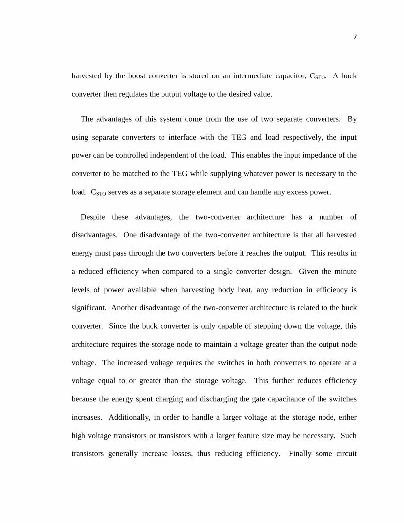
7
harvested by the boost converter is stored on an intermediate capacitor, CSTO. A buck
converter then regulates the output voltage to the desired value.
The advantages of this system come from the use of two separate converters. By
using separate converters to interface with the TEG and load respectively, the input
power can be controlled independent of the load. This enables the input impedance of the
converter to be matched to the TEG while supplying whatever power is necessary to the
load. CSTO serves as a separate storage element and can handle any excess power.
Despite these advantages, the two-converter architecture has a number of
disadvantages. One disadvantage of the two-converter architecture is that all harvested
energy must pass through the two converters before it reaches the output. This results in
a reduced efficiency when compared to a single converter design. Given the minute
levels of power available when harvesting body heat, any reduction in efficiency is
significant. Another disadvantage of the two-converter architecture is related to the buck
converter. Since the buck converter is only capable of stepping down the voltage, this
architecture requires the storage node to maintain a voltage greater than the output node
voltage. The increased voltage requires the switches in both converters to operate at a
voltage equal to or greater than the storage voltage. This further reduces efficiency
because the energy spent charging and discharging the gate capacitance of the switches
increases. Additionally, in order to handle a larger voltage at the storage node, either
high voltage transistors or transistors with a larger feature size may be necessary. Such
transistors generally increase losses, thus reducing efficiency. Finally some circuit
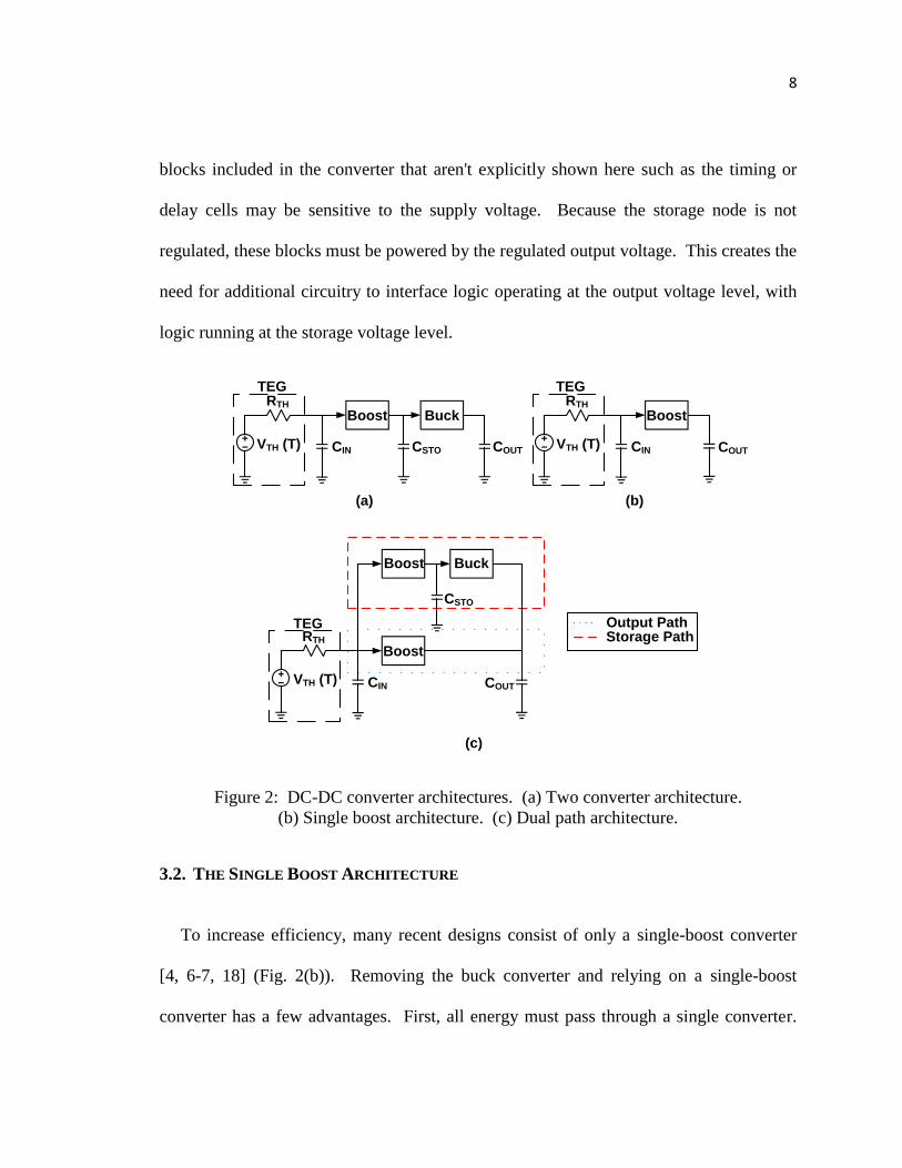
8
blocks included in the converter that aren't explicitly shown here such as the timing or
delay cells may be sensitive to the supply voltage. Because the storage node is not
regulated, these blocks must be powered by the regulated output voltage. This creates the
need for additional circuitry to interface logic operating at the output voltage level, with
logic running at the storage voltage level.
COUT
RTH
CIN
Boost
COUTVTH (T)
RTH
CIN CSTO
Boost Buck
(a) (b)
TEG TEG
RTH
CIN
Boost
COUT
Boost Buck
CSTO
TEG Output PathStorage Path
(c)
VTH (T)
VTH (T)
Figure 2: DC-DC converter architectures. (a) Two converter architecture.
(b) Single boost architecture. (c) Dual path architecture.
3.2. THE SINGLE BOOST ARCHITECTURE
To increase efficiency, many recent designs consist of only a single-boost converter
[4, 6-7, 18] (Fig. 2(b)). Removing the buck converter and relying on a single-boost
converter has a few advantages. First, all energy must pass through a single converter.
9
This increases efficiency by eliminating the losses in the second converter. In addition,
because there is no buck converter, no node voltage exceeds the output voltage.
Consequently, the switches in the converter can be driven with the lower output voltage,
reducing switching losses and eliminating the need for any interface circuitry.
The disadvantages of this architecture stem from the lack of isolation between the
input source and the load. Since the same converter interfaces to both the TEG and the
load, the power drawn from the TEG is directly proportional to the power delivered to the
load. The input impedance is, therefore, proportional to the load impedance and cannot
be set to an independent value. As a result, the perceived efficiency benefit of having a
single converter is cancelled out by the impedance mismatch and the absence of excess
storage capability. Ultimately, this reduces the total energy that can be harvested. As a
result, this architecture is not suitable for variable loads that may temporarily exceed the
TEG specifications or time intervals in which the TEG supplies less power (no matter
how brief).
3.3. THE DUAL-PATH ARCHITECTURE
Recently, a new architecture has been developed which is capable of achieving a high
efficiency while maintaining an impedance match and providing storage for excess energy
[5] (Fig. 2(c)). In this architecture, there are two paths for electricity to flow. When the
voltage at the output of the converter falls below the desired level, energy is routed from
the TEG to the load via a boost converter. This path is identical to the single-boost
10
architecture. When energy is not needed at the output, energy is routed to a storage node
instead by a second boost converter. During normal operation all energy flows from the
TEG through one of these two converters. During time intervals when the TEG produces
lower power or the load requires more power than usual, a buck converter can transfer
power from the storage node to the output.
The dual-path architecture as described above is a promising alternative to the single
and double converter architectures. Having one path between the TEG and the output
allows for high efficiency, while the second path allows for isolation between the input
and the load. This isolation allows the input resistance of the converter to be set
independent of the load conditions.
As in the two stage architecture discussed earlier, the storage node voltage must be
equal to or greater than the output voltage. To increase efficiency further, the high
voltage storage node must be eliminated. The next section proposes a new architecture
based on the existing dual-path architecture that eliminates the need for a high voltage
storage node.
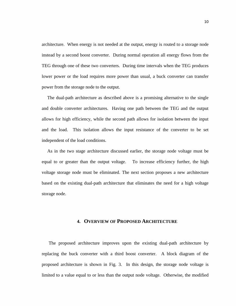
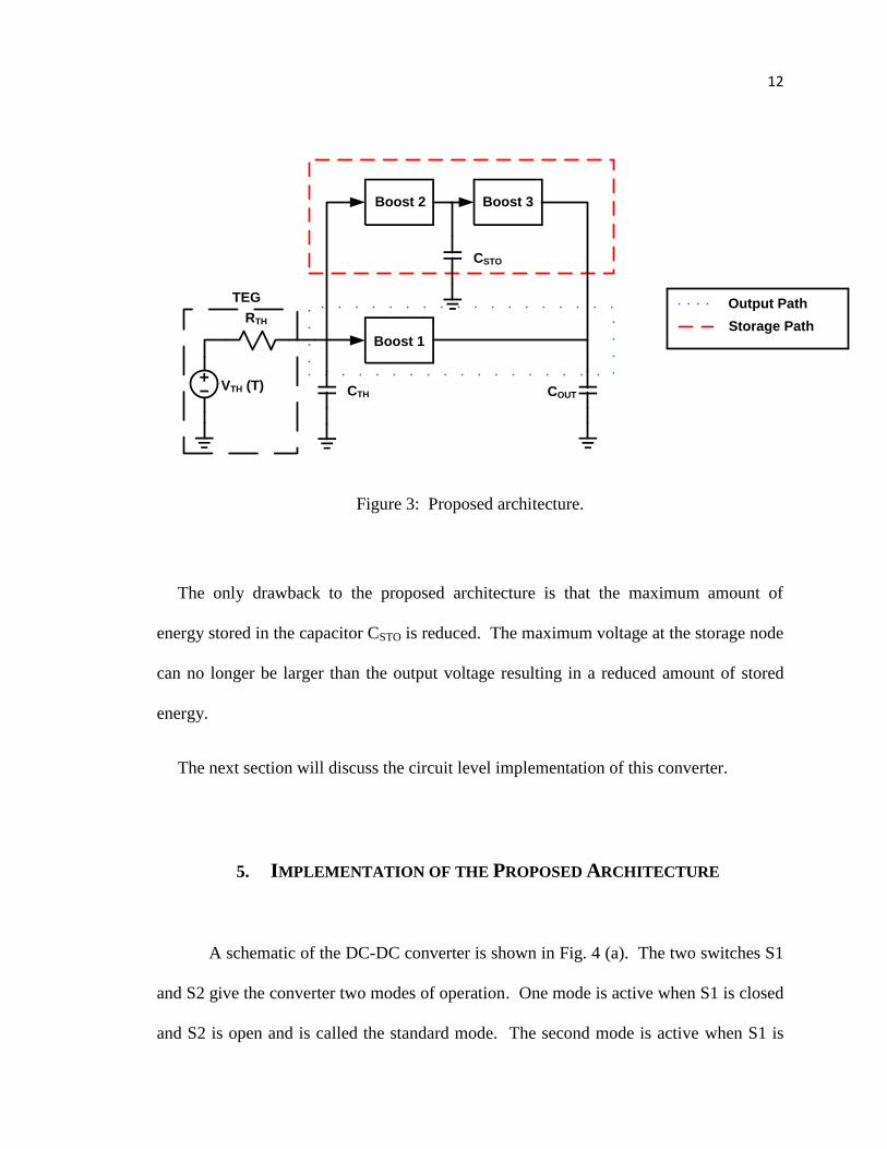
4. OVERVIEW OF PROPOSED ARCHITECTURE
The proposed architecture improves upon the existing dual-path architecture by
replacing the buck converter with a third boost converter. A block diagram of the
proposed architecture is shown in Fig. 3. In this design, the storage node voltage is
limited to a value equal to or less than the output node voltage. Otherwise, the modified

11
converter operates identically to the original dual-path converter. One boost converter
(Boost 1) transfers energy directly from the TEG to the output when needed. A second
boost converter (Boost 2) handles excess energy not needed at the load. The only
difference in this architecture is that the buck converter used in the prior system to
transport energy from the storage node to the output node is replaced by a boost converter
(Boost 3).
The proposed architecture has a key feature not available in the previous dual-path
architecture. As the storage node is held to a voltage no greater than the output voltage,
all switches can be driven by the output voltage. This results in a number of advantages
over the original dual-path architecture. First, the transistors can be implemented using a
smaller feature size. Second, all digital circuitry can use the same voltage supply avoiding
the need for interface circuitry. Third, since no blocks are powered by the storage node
voltage, the storage capacitor can be completely discharged and the system will still
operate.
12
VTH (T)
RTH
CTH
Boost 1
COUT
Boost 2 Boost 3
CSTO
TEG Output Path
Storage Path
Figure 3: Proposed architecture.
The only drawback to the proposed architecture is that the maximum amount of
energy stored in the capacitor CSTO is reduced. The maximum voltage at the storage node
can no longer be larger than the output voltage resulting in a reduced amount of stored
energy.
The next section will discuss the circuit level implementation of this converter.
5. IMPLEMENTATION OF THE PROPOSED ARCHITECTURE
A schematic of the DC-DC converter is shown in Fig. 4 (a). The two switches S1
and S2 give the converter two modes of operation. One mode is active when S1 is closed
and S2 is open and is called the standard mode. The second mode is active when S1 is
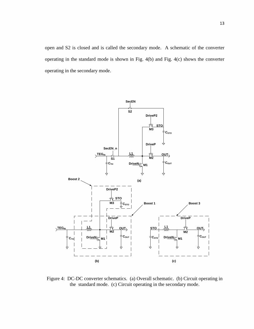
13
open and S2 is closed and is called the secondary mode. A schematic of the converter
operating in the standard mode is shown in Fig. 4(b) and Fig. 4(c) shows the converter
operating in the secondary mode.
DriveN
DriveP
OUTSTO L1
COUTCSTO
(c)
DriveN
DriveP
DriveP2
STO
OUTTEGINL1
CTHCOUT
CSTO
(a)
S1
S2
SecEN_n
SecEN
M1
M2
M3
M1
M2
TEGIN
CTH
(b)
DriveN
DriveP
DriveP2
STO
OUTL1
COUT
CSTO
M1
M2
M3 Boost 1
Boost 2
Boost 3
Figure 4: DC-DC converter schematics. (a) Overall schematic. (b) Circuit operating in
the standard mode. (c) Circuit operating in the secondary mode.
14
The converter operates in the standard mode as long as the output voltage remains
above 1.25V. This value was selected because it is close to the desired output voltage of
1.3V, indicating the converter is keeping up with the power requirements of the load.
The precise value is set by two external resistors (not shown) and can be adjusted if
required. During the standard mode, the TEG is connected to the inductor L1 through the
switch S1. Energy is gathered from the TEG and either transferred to the output through
Boost 1 (if the output voltage VOUT falls below 1.3V), or to the storage node through
Boost 2 (if VOUT is above 1.3V). Since energy is never transferred to both the output
node and the storage node at the same time, the inductor L1 and the NMOS (or low-side)
switch M1 can be shared between Boost 1 and Boost 2. M2 serves as the PMOS (or
high-side) switch for Boost 1 whereas M3 serves as the high-side switch for Boost 2.
Boost 3 is not needed during the standard mode since the primary purpose of Boost 3 is
to provide energy to the output when the TEG is incapable of providing sufficient power.
Since the converter only operates in the standard mode when the TEG is supplying
sufficient power, only Boost 1 and Boost 2 are required.
The secondary mode is activated when VOUT falls below 1.25V. Since the
converter is designed to regulate the output voltage to 1.3V, an output voltage of 1.25V
indicates the converter is struggling to keep up with load power demands. When VOUT
falls below 1.25V, switch S1 is opened and switch S2 is closed. This disconnects the
TEG from the inductor and connects the storage node capacitor in its place. Boost 3 can
then be formed using the same transistors (M1 and M2) that are used to form Boost 1
when the converter is operating in the standard mode. Boost 1 and Boost 2 are not

15
functional during the secondary mode since both converters draw energy from the TEG
which is not connected during the secondary mode. Once the secondary mode is enabled,
the converter will operate in the secondary mode until VOUT climbs above 1.3V (Fig. A-6
Appendix F). At that point, switch S1 will be closed, and switch S2 will be opened,
returning the converter to the standard mode.
A detailed description of the controls for this converter is given in Appendix D.
Sections 5.1 and 5.2 discuss the pulse and oscillator blocks which are responsible for
controlling the timing of the control circuitry. Both the oscillator and pulse blocks are
also essential for setting the input impedance of the converter which will be discussed in
Section 5.1.
5.1. DESIGN FOR IMPEDANCE MATCH
The input resistance for a standard inductor based boost converter operating in
discontinuous conduction mode [31] is shown in [3-4] and is given by:
where L is the inductance, FS is the switching frequency for the NMOS switch, and D is
the duty cycle of the NMOS switch. For a duty cycle of 50%, the input resistance is
given by:
16
It is important that the input resistance of the converter matches the output resistance of
the TEG for maximum power transfer.
As seen in (3), the inductance, the frequency, or both must be increased as the
desired value of RIN is increased. Large resistances can be difficult to match for two
reasons. First, body powered devices should be small and compact to avoid discomfort
for the wearer [2, 17]. As a result, the physical size and value of the inductor are limited.
Second, a higher frequency increases the power consumption in both the clocking and
control circuitry of the converter. This suggests why most prior designs have focused on
converters with a very low output resistance (10 ohms or less) [3, 6-7, 18].
One way to increase RIN is to decrease the duty cycle of the NMOS switch, i.e.,
every Nth clock cycle drives the switch. References [4] and [5] have shown that when the
NMOS switch is driven every Nth clock cycle, the RIN of the converter is given by:
where D is the duty cycle of the clock. For a clock with a 50% duty cycle, RIN can be
rewritten as:
Previously, pulse counting was used as a way to harvest energy from multiple
converters simultaneously in a time-interleaved fashion. From (5) it is seen that pulse
17
counting may also be used to achieve the required input impedance with a lower clock
frequency. When the NMOS switch is clocked every Nth pulse, the clock frequency is
reduced by a factor of N while L and RIN are held constant. This design modification can
reduce the power consumed in the clock circuitry. Additionally, with most circuitry
operated every Nth clock cycle, and the clock operating at 1/N times its original
frequency, the switching power consumption is reduced by a factor of approximately N2.
Despite these advantages, pulse counting has one major disadvantage. As the
value of N increases, the time between periods where energy is harvested from the TEG
also increases. This can increase the ripple voltage at the output and decrease the
converter’s handling of variable loads. If a large load current occurs between periods
where energy is harvested, the converter may be unable to provide the load any power.
This may occur even if the average power of the load falls below the level of power the
TEG can supply.
To match the input impedance of the converter to a TEG with a high output
impedance (20kΩ), pulse counting was implemented. To keep the design small and
compact, the physical size of the inductor was limited to the size of the TEG
(~0.5”x0.5”). An 820 μH inductor was used for L1. As a benchmark, the converter was
designed to transfer energy at a rate greater than once per millisecond. During normal
operation, the value of N was set to 32 and the frequency, FS, was set to 100 kHz. With
these values for N and Fs, energy is harvested once every 320 μs. Using (5), the RIN of
the converter for the given values of N, Fs, and L is approximately 20kΩ.

18
During the secondary mode, the TEG is disconnected from the circuit so, no
impedance matching is necessary. As no energy is extracted from the TEG, it is critical
to limit the time the converter operates in the secondary mode. N is, therefore, reduced to
4 during the secondary mode. This reduces the input impedance of the converter seen by
the storage node. The reduced input impedance increases the rate at which energy can be
transferred from the storage node to the output node resulting in a faster charging of the
load capacitor. Details of the pulse counting circuitry can be found in Appendix E.
The next section discusses the design of a new current-starved ring oscillator
topology which is used for clocking the converter.
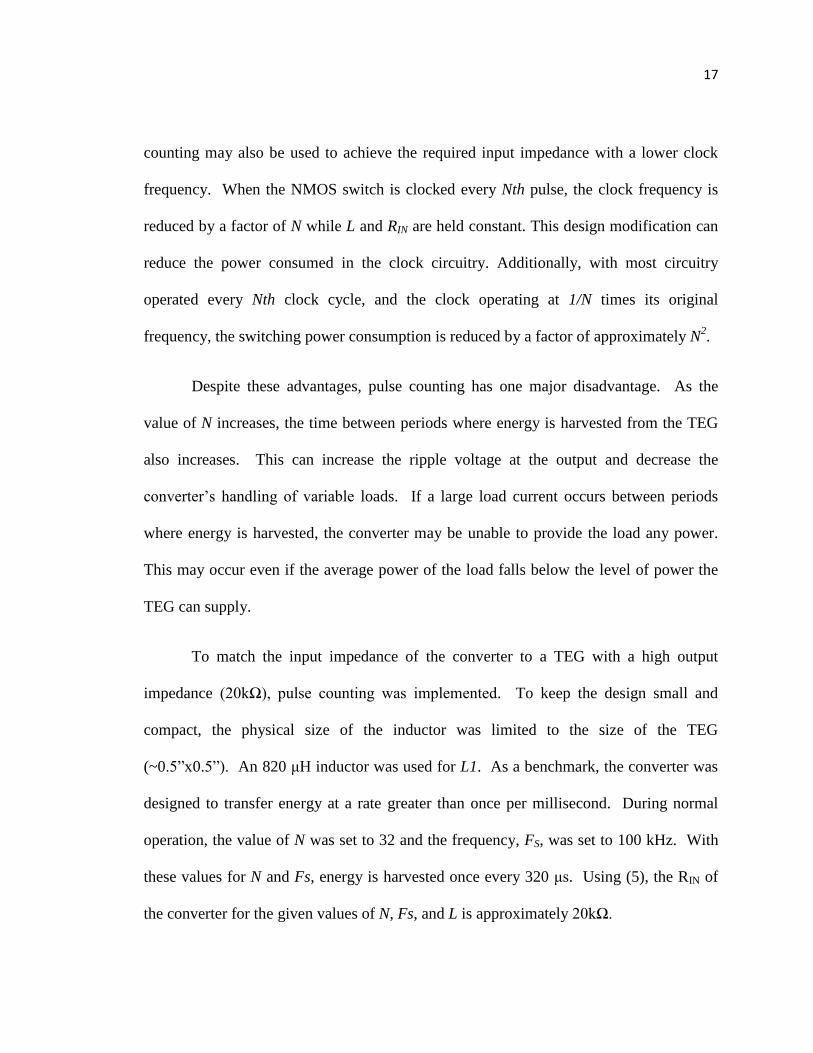
5.2. LOW-POWER RING OSCILLATOR
For many low power converters the clock represents a large portion of the
system’s total power consumption [18]. A careful design must be done to minimize the
power consumed by the clock. In this application, a low-power, current-starved ring
oscillator has been developed to reduce the power consumption of the clock.
Although current-starved oscillators can be very efficient, their output voltage
does not swing rail-to-rail [32]. As a result, a current-starved oscillator is typically
followed by a self-biased inverter, followed by a chain of standard inverters to buffer the
signal and obtain a full output swing. A schematic of a typical current-starved oscillator
which utilizes a self-biased inverter is shown in Fig. 5. The self-biased inverter is biased
19
at its trip point. This ensures that any oscillation, no matter how small, will cross the trip
point of the self-biased inverter, providing a rail-to-rail output swing.
Ring Oscillator Buffer
C
R
Clk
Self-biased
inverter
Figure 5: Typical current-starved ring oscillator.
The power consumption of a self-biased inverter can be large. Since both
transistors conduct current at the trip point, a considerable amount of quiescent power is
consumed. The resistor and capacitor in the self-biased inverter (Fig. 5) form a high-pass
filter. In order to pass a low frequency signal, the values of R and C can be large which
would require larger die area.
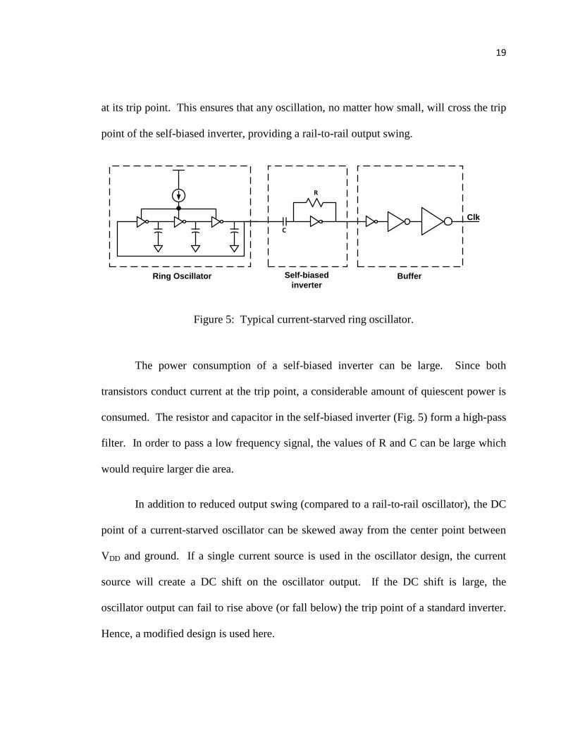
In addition to reduced output swing (compared to a rail-to-rail oscillator), the DC
point of a current-starved oscillator can be skewed away from the center point between
VDD and ground. If a single current source is used in the oscillator design, the current
source will create a DC shift on the oscillator output. If the DC shift is large, the
oscillator output can fail to rise above (or fall below) the trip point of a standard inverter.
Hence, a modified design is used here.
20
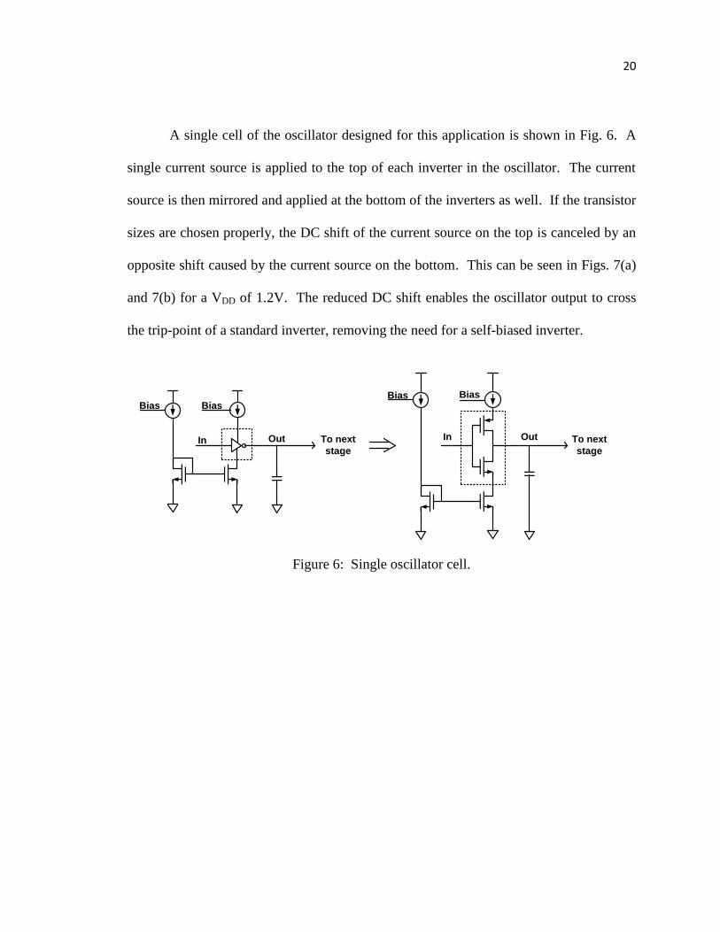
A single cell of the oscillator designed for this application is shown in Fig. 6. A
single current source is applied to the top of each inverter in the oscillator. The current
source is then mirrored and applied at the bottom of the inverters as well. If the transistor
sizes are chosen properly, the DC shift of the current source on the top is canceled by an
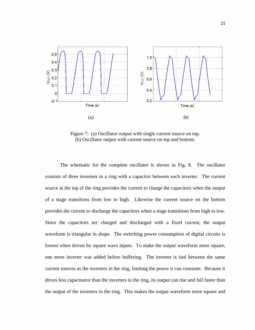
opposite shift caused by the current source on the bottom. This can be seen in Figs. 7(a)
and 7(b) for a VDD of 1.2V. The reduced DC shift enables the oscillator output to cross
the trip-point of a standard inverter, removing the need for a self-biased inverter.
In To next
stage
OutOut To next
stage
Bias
In
BiasBiasBias
Figure 6: Single oscillator cell.
21
(a) (b)
Figure 7: (a) Oscillator output with single current source on top.
(b) Oscillator output with current source on top and bottom.
The schematic for the complete oscillator is shown in Fig. 8. The oscillator
consists of three inverters in a ring with a capacitor between each inverter. The current
source at the top of the ring provides the current to charge the capacitors when the output
of a stage transitions from low to high. Likewise the current source on the bottom
provides the current to discharge the capacitors when a stage transitions from high to low.
Since the capacitors are charged and discharged with a fixed current, the output
waveform is triangular in shape. The switching power consumption of digital circuits is
lowest when driven by square wave inputs. To make the output waveform more square,
one more inverter was added before buffering. The inverter is tied between the same
current sources as the inverters in the ring, limiting the power it can consume. Because it
drives less capacitance than the inverters in the ring, its output can rise and fall faster than
the output of the inverters in the ring. This makes the output waveform more square and
22
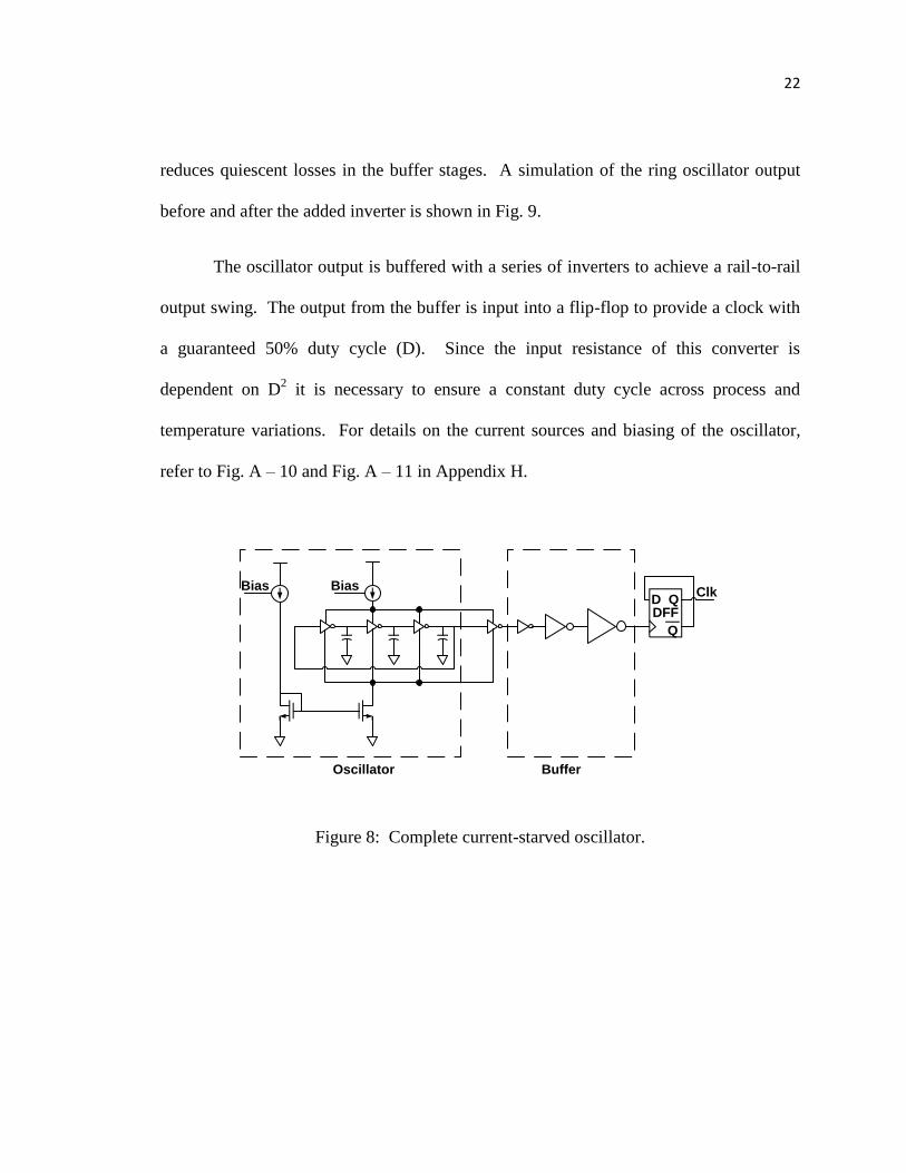
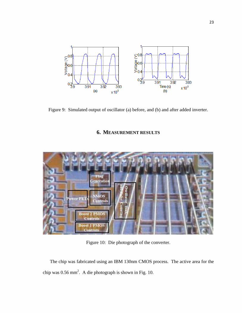
reduces quiescent losses in the buffer stages. A simulation of the ring oscillator output
before and after the added inverter is shown in Fig. 9.
The oscillator output is buffered with a series of inverters to achieve a rail-to-rail
output swing. The output from the buffer is input into a flip-flop to provide a clock with
a guaranteed 50% duty cycle (D). Since the input resistance of this converter is
dependent on D2 it is necessary to ensure a constant duty cycle across process and
temperature variations. For details on the current sources and biasing of the oscillator,
refer to Fig. A – 10 and Fig. A – 11 in Appendix H.
Clk
DFFD Q
Q
BiasBias
Oscillator Buffer
Figure 8: Complete current-starved oscillator.
23
Figure 9: Simulated output of oscillator (a) before, and (b) and after added inverter.
6. MEASUREMENT RESULTS
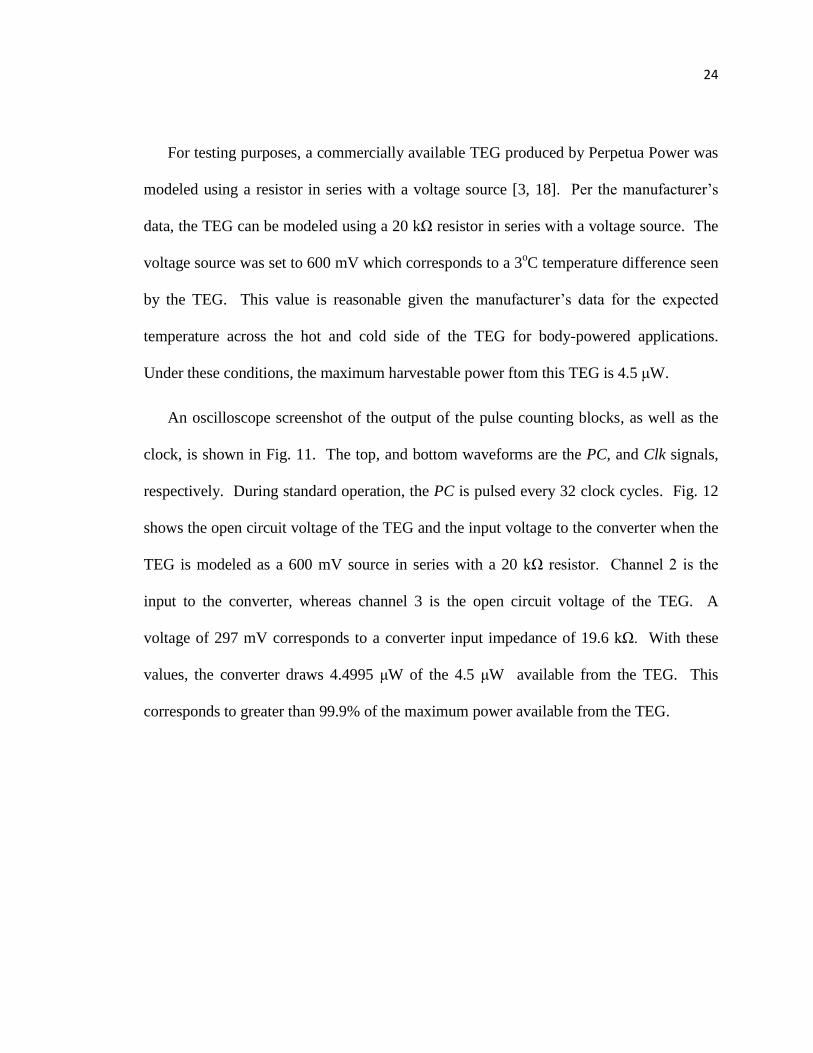
Figure 10: Die photograph of the converter.
The chip was fabricated using an IBM 130nm CMOS process. The active area for the
chip was 0.56 mm2. A die photograph is shown in Fig. 10.
24
For testing purposes, a commercially available TEG produced by Perpetua Power was
modeled using a resistor in series with a voltage source [3, 18]. Per the manufacturer’s
data, the TEG can be modeled using a 20 kΩ resistor in series with a voltage source. The
voltage source was set to 600 mV which corresponds to a 3oC temperature difference seen
by the TEG. This value is reasonable given the manufacturer’s data for the expected
temperature across the hot and cold side of the TEG for body-powered applications.
Under these conditions, the maximum harvestable power ftom this TEG is 4.5 μW.
An oscilloscope screenshot of the output of the pulse counting blocks, as well as the
clock, is shown in Fig. 11. The top, and bottom waveforms are the PC, and Clk signals,
respectively. During standard operation, the PC is pulsed every 32 clock cycles. Fig. 12
shows the open circuit voltage of the TEG and the input voltage to the converter when the
TEG is modeled as a 600 mV source in series with a 20 kΩ resistor. Channel 2 is the
input to the converter, whereas channel 3 is the open circuit voltage of the TEG. A
voltage of 297 mV corresponds to a converter input impedance of 19.6 kΩ. With these
values, the converter draws 4.4995 μW of the 4.5 μW available from the TEG. This
corresponds to greater than 99.9% of the maximum power available from the TEG.
25
1.3V
PC
Clk
320 μS (32 clock pulses)
Vo
lta
ge
(V)
Time (s)
0V
0V
1.3V
Figure 11: Clock and pulse-counting signals.
0V
0V
Time (s)
Volt
age
(V) 601 mV
297 mV
Open-circuit voltage = 601 mV
VTEG = 297 mV
RIN ~ 19.5 kilo ohms
PTEG-OUT > 0.999*PTEG-MAX
Figure 12: Open-circuit TEG voltage and converter input voltage.
Fig. 13 shows an oscilloscope waveform of the gate voltages of the NMOS and PMOS
switches. During this test, the output of the converter was loaded with a 1 μW load. In
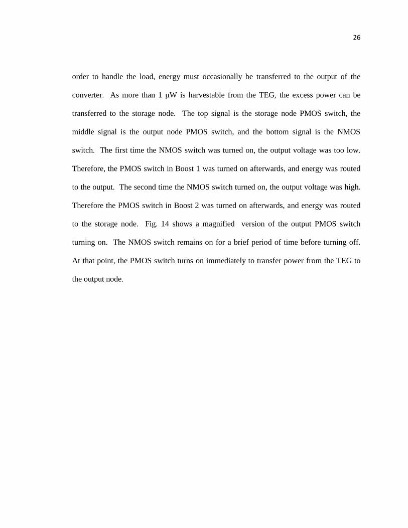
26
order to handle the load, energy must occasionally be transferred to the output of the
converter. As more than 1 μW is harvestable from the TEG, the excess power can be
transferred to the storage node. The top signal is the storage node PMOS switch, the
middle signal is the output node PMOS switch, and the bottom signal is the NMOS
switch. The first time the NMOS switch was turned on, the output voltage was too low.
Therefore, the PMOS switch in Boost 1 was turned on afterwards, and energy was routed
to the output. The second time the NMOS switch turned on, the output voltage was high.
Therefore the PMOS switch in Boost 2 was turned on afterwards, and energy was routed
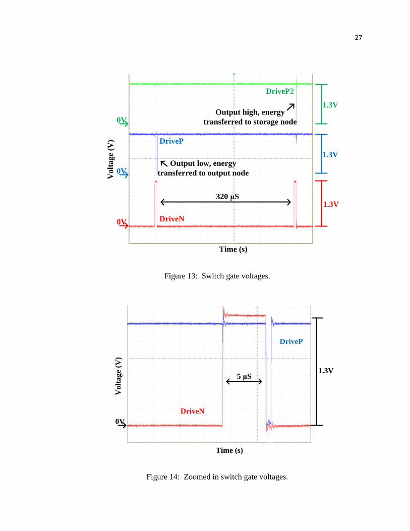
to the storage node. Fig. 14 shows a magnified version of the output PMOS switch
turning on. The NMOS switch remains on for a brief period of time before turning off.
At that point, the PMOS switch turns on immediately to transfer power from the TEG to
the output node.
27
Time (s)
Vo
lta
ge
(V)
0V
0V
0V
1.3V
1.3V
1.3V
DriveN
DriveP
DriveP2
Output low, energy
transferred to output node
Output high, energy
transferred to storage node
320 μS
Figure 13: Switch gate voltages.
0V
1.3V
DriveN
DriveP
5 μS
Time (s)
Volt
age
(V)
Figure 14: Zoomed in switch gate voltages.
28
Because of problems encountered during testing of the chip, it was not possible to use
the internal oscillator during power measurements. Instead, the idle power consumption
of the oscillator was measured to be 186 nW. The circuit was then tested using an external
oscillator. To obtain the final results, the idle power consumption of the internal oscillator
was added to the power consumption of the circuit under each load. The performance of
the converter over different load conditions is shown in Fig. 15.
Figure 15: Standard mode performance of the converter.
With an available input power of 4.5 μW, the chip is capable of providing a combined
2.71 μW to the storage node and output. This corresponds to an efficiency of 60.2%. For
0
10
20
30
40
50
60
70
80
90
0 2 4 6 8 10 12 14 16
Effi
cie
ncy
(%
)
Load (μW)
29
a 5 μW load, the converter requires 7.33 μW of input power, whereas a 1 μW load can be
powered with only 2.32 μW of input power. The maximum efficiency occurs with a load
of 14 μW and is 84%.
Table 1 compares these values to other state-of-the-art DC-DC converters. Converter
efficiency is the measure of the load power divided by the input power. To show the
advantages of impedance matching, end-to-end efficiency is also shown. End-to-end
efficiency was defined in [3] to be the output power divided by the maximum power
available from the TEG. Even though the efficiency of [18] is high at low load power
levels (1-5 μW), it is only capable of achieving this efficiency when the maximum
harvestable power from the TEG is 25 μW or higher. Consequently, the end-to-end
efficiency is low despite the high converter efficiency. Real body-powered TEGs may not
be able to provide 25 μW of power making the architecture shown in [18] unsuitable for
body powered applications. The work shown in [7] also has a high efficiency, but only
with load power levels (3 mW) that exceed the capability of body-powered designs. The
converter shown in this work is capable of achieving a high end-to-end efficiency at lower
power levels of 1-5 μW. High end-to-end maximizes the power delivered to the load even
with low available power from the TEG.
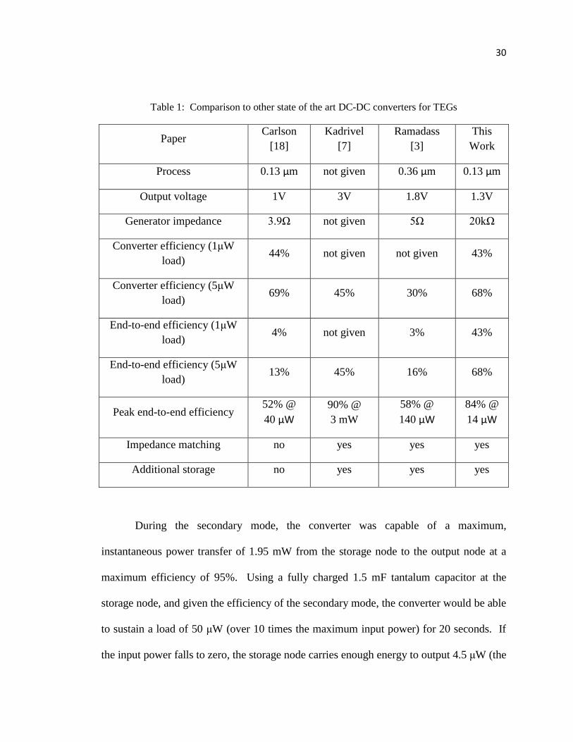
30
Table 1: Comparison to other state of the art DC-DC converters for TEGs
Paper Carlson
[18]
Kadrivel
[7]
Ramadass
[3]
This
Work
Process 0.13 μm not given 0.36 μm 0.13 μm
Output voltage 1V 3V 1.8V 1.3V
Generator impedance 3.9Ω not given 5Ω 20kΩ
Converter efficiency (1μW
load) 44% not given not given 43%
Converter efficiency (5μW
load) 69% 45% 30% 68%
End-to-end efficiency (1μW
load) 4% not given 3% 43%
End-to-end efficiency (5μW
load) 13% 45% 16% 68%
Peak end-to-end efficiency 52% @
40 μW
90% @
3 mW
58% @
140 μW
84% @
14 μW
Impedance matching no yes yes yes
Additional storage no yes yes yes
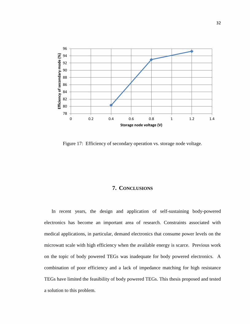
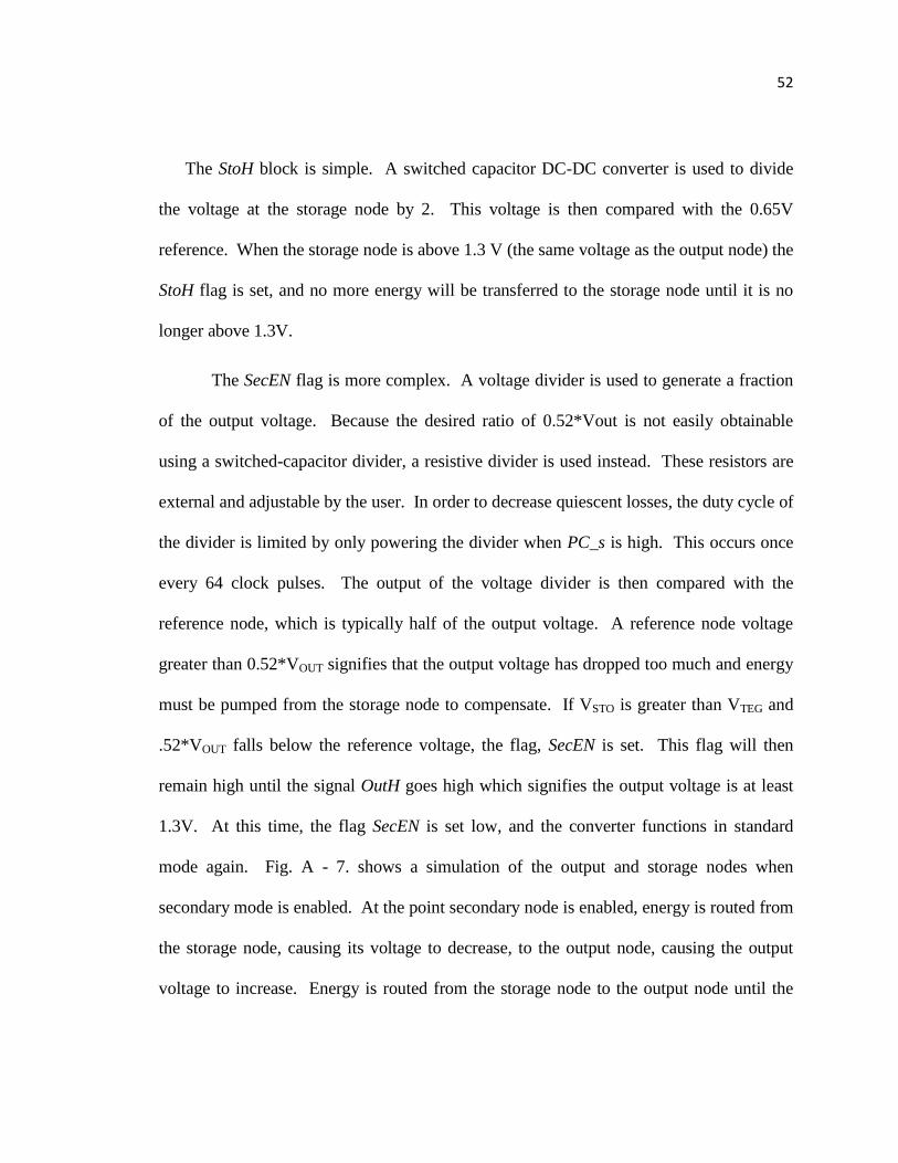
During the secondary mode, the converter was capable of a maximum,
instantaneous power transfer of 1.95 mW from the storage node to the output node at a
maximum efficiency of 95%. Using a fully charged 1.5 mF tantalum capacitor at the
storage node, and given the efficiency of the secondary mode, the converter would be able
to sustain a load of 50 μW (over 10 times the maximum input power) for 20 seconds. If
the input power falls to zero, the storage node carries enough energy to output 4.5 μW (the
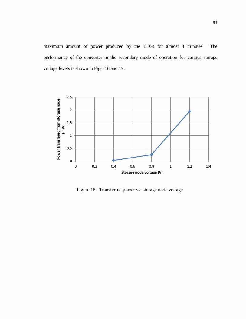
31
maximum amount of power produced by the TEG) for almost 4 minutes. The
performance of the converter in the secondary mode of operation for various storage
voltage levels is shown in Figs. 16 and 17.
Figure 16: Transferred power vs. storage node voltage.
0
0.5
1
1.5
2
2.5
0 0.2 0.4 0.6 0.8 1 1.2 1.4
Po
we
r tr
ansf
ere
d f
rom
sto
rage
no
de
(m
W)
Storage node voltage (V)
32
Figure 17: Efficiency of secondary operation vs. storage node voltage.
7. CONCLUSIONS
In recent years, the design and application of self-sustaining body-powered
electronics has become an important area of research. Constraints associated with
medical applications, in particular, demand electronics that consume power levels on the
microwatt scale with high efficiency when the available energy is scarce. Previous work
on the topic of body powered TEGs was inadequate for body powered electronics. A
combination of poor efficiency and a lack of impedance matching for high resistance
TEGs have limited the feasibility of body powered TEGs. This thesis proposed and tested
a solution to this problem.
78
80
82
84
86
88
90
92
94
96
0 0.2 0.4 0.6 0.8 1 1.2 1.4
Effi
cie
ncy
of
seco
nd
ary
mo
de
(%
)
Storage node voltage (V)
33
A DC-DC boost converter capable of operating at power levels below 5 μW was
presented. The converter uses a low duty cycle to support TEGs that exhibit large output
impedances. A dual-path architecture has been implemented, allowing the converter to
store excess energy and use it when the load exceeds the TEG’s output capacity. The
system consumes less than 900 nW of power while idle, and 1.3 μW while connected to a
1 μW load, making it suitable for body-powered applications.
34
BIBLIOGRAPHY
[1] J. Kymissis, C. Kendall, J. Paradiso, and N. Gershenfeld, “Parasitic power harvesting
in shoes,” Proc. of the Second IEEE International Conf. on Wearable Computing, pp.
132-139, Oct. 1998.
[2] V. Leonov, T. Torfs, P. Fiorini, and C. Van Hoof, “Thermoelectric converters of
human warmth for self-powered wireless sensor nodes,” IEEE Sensors Journal, vol. 7,
no. 5, pp. 650-657, May 2007.
[3] Y. Ramadass and A. Chandrakasan, “A batteryless thermoelectric energy-harvesting
interface circuit with 35mV startup voltage,” IEEE J. Solid-State Circuits, vol. 46 no. 1
pp. 333-341, Jan. 2011.
[4] C. Shi, B. Miller, K. Mayaram, and T. Fiez, “A multiple-input boost converter for
low-power energy harvesting,” IEEE Trans. On Circuits and Systems-II: Express Briefs,
vol. 58 no. 12, pp. 827-831, Dec. 2011.
[5] S. Bandyopadhyay and A. Chandrakasan, “Platform architecture for solar, thermal
and vibrational energy combining with MPPT and single inductor,” Symposium on VLSI
Circuits, pp. 238-239, Jun. 2011.
[6] J. Im, S. Wang, K. Lee, Y. Woo, Y. Yuk, T. Kong, S. Hong, S. Ryu, and G. Cho “A
40mV transformer-reuse self-startup boost converter with MPPT control for
thermoelectric energy harvesting,” ISSCC Dig. Tech. Papers, pp 105-106, Feb. 2012.
[7] K. Kadrivel, Y. Ramadass, U. Lyles, J. Carpenter, V. Ivanov, V. McNeil, A.
Chandrakasan, and B. Lum-Shue-Chan, “A 330nA energy-harvesting charger with
battery management for solar and thermoelectric energy harvesting,” ISSCC Dig. Tech.
Papers, pp 106-107, Feb. 2012.
[8] K. Finkenzeller, RFID Handbook: Fundamentals and Applications in Contactless
Smart Cards and Identification, John Wiley, Chicester, Sussex, Second edition, 2003.
[9] A. L. Annala, I. Oy, and U. Friedrich, “Passive long distance multiple access UHF
RFID system (RFID),” Palomar Project, European Commission, Public Report, Project
Number IST1999-10339, Nov. 2002.
35
[10] S. H. Wright, “MIT duo sees people-powered ‘Crowd Farm,’" MIT news, Internet:
http://web.mit.edu/newsoffice/2007/crowdfarm-0725.html, Jul. 2007 [Jan. 12, 2012].
[11] A. Kannampilly, “How to save the world one dance at a time,” ABC News, Internet:
http://abcnews.go.com/International/story?id=5358214&page=1, Jul. 2008 [Jan. 12,
2012].
[12] S. Cornwall, “Solar Powered Technology: 5 Reasons to Purchase a Solar Powered
Watch,” Ezine Articles, Internet: http://ezinearticles.com/?Solar-Powered-Technology:-5-
Reasons-to-Purchase-a-Solar-Powered-Watch&id=7360689, Nov. 2012 [Jan. 12, 2003].
[13] D. D. Sumner, C. M. Whitaker, and L. E. Schlueter, "Carrisa plains photovoltaic
power plant 1984-7 performance," Photovoltaic Specialists Conf., 1988., Conf. Record of
the Twentieth IEEE, vol. 2, pp. 1289-1292
[14] J. P. Fleurial, P. Gogna, B.C. Li, S. Firdosy, B. J. Chen, C. K. Huang, V. Ravi, T.
Caillat, and K. Star, “Waste heat recovery opportunities for thermoelectric generators,”
NASA JPL 2009 Thermoelectric Applications Workshop, Sep. 2009
[15] Y. Lin, D. Sylvester, and D. Blaauw, “An ultra low power 1V, 220nW temperature
sensor for passive wireless applications,” CICC, pp. 507-510, Sep. 2008.
[16] Panassonic Electric Works Corporation of America, “Passive infared motion
sensor,” EKMB11 datasheet
[17] V. Leonov and R. J. M. Vullers, “Wearable thermoelectric generators for body-
powered devices,” J. of Electronic Materials, vol. 38, no. 7, pp. 1491-1498, Nov. 2009.
[18] E. J. Carlson, K. Strunz, and B. P. Otis, “A 20 mV input boost converter with
efficient digital control for thermoelectric energy harvesting,” IEEE J. Solid State
Circuits, vol. 45 no. 4 pp. 741-751, Apr. 2010.
[19] Tellurex Corporation, “Thermoelectric module specifications,” G2-30-0313
datasheet
[20] Micropelt GmbH, “Thin film thermogenerators and sensing devices,” MPG-D571
datasheet
[21] M. D. Seeman, “Analytical and practical analysis of switched-capacitor DC-DC
converters,” Masters Thesis, University of California, Berkeley, Berkeley, CA,
Department of Electrical Engineering and Computer Science, 2006.
36
[22] M. Lee, W. Dally, and P. Chiang, “Low power area efficient high-speed I/O circuit
techniques,” IEEE J. Solid-State Circuits, vol. 35, no. 11, pp. 1591-1599, Nov. 2000.
[23] “Dietary guidelines for Americans, 2010,” U.S. Department of Health and Human
Services, Jan. 2011.
[24] O. C. Ozcanli, “Turning body heat into electricity,” Internet:
http://www.forbes.com/2010/06/07/nanotech-body-heat-technology-breakthroughs-
devices.html, Jun. 2010 [Aug. 24, 2012].
[25] S. D. Baker, J. Verweij, E. K. Rowinsky, R. C. Donehower, J. H. Schellens, L. B.
Grochow, and A. Sparreboom, ”Role of body surface area in dosing of investigational
anticancer agents in adults, 1991–2001,” J. Natl. Cancer Inst., vol. 94, no. 24, Dec. 2002.
[26] D. A. Kaminski, and M. K. Jensen, “Thermodynamic cycles and the second law,”
Introduction to Thermal and Fluid Engineering, Hoboken, NJ: Wiley, 2005, pp. 257-318.
[27] W. D. Jones, “Super soaker inventor invents new thermoelectric generator,” Internet:
http://spectrum.ieee.org/semiconductors/devices/super-soaker-inventor-invents-new-
thermoelectric-generator, Mar. 2008 [Aug. 23, 2012].
[28] J. M. Wiesse, “Thermoelectric generators,” class notes for Physics 240, Department
of Physics, Stanford University, Oct. 2010.
[29] D. L. Chandler, “Turning heat to electricity,” MIT news, Internet:
http://web.mit.edu/newsoffice/2009/thermoelectric.html, Nov. 2009 [Aug. 24, 2012].
[30] J. Hope, and C. Bates, “On sale, smart pill with ‘edible microchip’ that tells you and
your doctor when the next dose is due,” internet:
http://www.dailymail.co.uk/health/article-2087275/New-smart-pill-tells-patients-dose-
due.html, Jan. 2012 [Aug. 31, 2012].
[31] R. W. Erickson, and D. Maksimovic, “The discontinuous conduction mode,”
Fundamentals of Power Electronics 2nd
Ed., New York, NY: Springer, pp. 107-130.
[32] P. K. Hanumolu “ECE599: Phase-Locked Loops,” class notes for ECE 599,
Department of Electrical Engineering and Computer Science, Oregon State University,
Sep. 2012.

37
APPENDICES
38
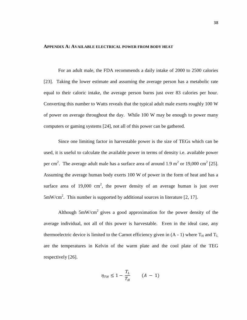
APPENDIX A: AVAILABLE ELECTRICAL POWER FROM BODY HEAT
For an adult male, the FDA recommends a daily intake of 2000 to 2500 calories
[23]. Taking the lower estimate and assuming the average person has a metabolic rate
equal to their caloric intake, the average person burns just over 83 calories per hour.
Converting this number to Watts reveals that the typical adult male exerts roughly 100 W
of power on average throughout the day. While 100 W may be enough to power many
computers or gaming systems [24], not all of this power can be gathered.
Since one limiting factor in harvestable power is the size of TEGs which can be
used, it is useful to calculate the available power in terms of density i.e. available power
per cm2. The average adult male has a surface area of around 1.9 m
2 or 19,000 cm
2 [25].
Assuming the average human body exerts 100 W of power in the form of heat and has a
surface area of 19,000 cm2, the power density of an average human is just over
5mW/cm2. This number is supported by additional sources in literature [2, 17].
Although 5mW/cm2
gives a good approximation for the power density of the
average individual, not all of this power is harvestable. Even in the ideal case, any
thermoelectric device is limited to the Carnot efficiency given in (A - 1) where TH and TL
are the temperatures in Kelvin of the warm plate and the cool plate of the TEG
respectively [26].
39
Assuming that the human body is roughly 37 oC (about 98
oF), and the ambient
temperature is 10 oC cooler, the maximum efficiency of any thermoelectric device is only
3%. This reduces the maximum power harvestable from body heat to a density of around
170μW/cm2.
It is important to recognize 170μW/cm2 represents the maximum harvestable
power in an ideal case. Using existing components and realistic environmental
conditions the actual harvestable power is reduced. Published reports indicate current
TEGs operate at no more than 20% of the Carnot efficiency [27-28], and according to
some sources may not even exceed 10% of that limit [29]. Additionally the thermal
connection between the skin and the TEG was assumed to be ideal and capable of
creating a 10 oC difference between the hot and cold plates of the TEG. The core body
temperature for most individuals is typically around 37 oC [2, 17], but the surface of the
skin can be cooler. Since the skin is exposed to external conditions, not only can it be
cooled by the surrounding air, but heat released through the skin can heat the air around it
as well. The actual temperature difference across the TEG can be less than 1 oC unless
the use of a bulky and cumbersome heat sink is used [2, 17]. Assuming a TEG that
achieves 20% of the Carnot efficiency and a reduced temperature difference of only 1 oC,
the maximum power reasonably obtainable from a body-powered TEG is reduced to
3.3μW/cm2.
Using the average surface area of the adult male at 19,000 cm2, if the entire body
was covered with TEGs, only 63mW could be harvested. In practice this number is

40
optimistic as only a limited area of the body can be covered by TEGs without causing
discomfort. In studies, a body-powered EEG device only 50 cm2 in area created an
overwhelmingly cool sensation for the test subjects [2, 17]. By limiting the size of TEGs
used to well below 50 cm2 in order to reduce discomfort, the harvestable power may be
reduced to power levels below the tens of micro-Watts previously assumed to be
harvestable [3, 18].

41
APPENDIX B: TESTING DETAILS
A total of seventeen units were tested. Table A - 1 provides an overview of each
chip’s functionality. Failure mechanisms in the control loop varied from chip to chip and
are combined into a single category.
Table A - 1: Overview of chip functionality
One possible cause of the oscillator’s failures might be due to the current-starved ring
design. With such designs, it is possible that the oscillation from the oscillator fails to
cross the trip point of the buffers that follow. This potential problem is often avoided by
using a self-biased inverter as the first stage of the buffer to guarantee the signal passes
the trip point of the first inverter. This technique was not used in an attempt to lower
power consumption of the oscillator. As a result, the oscillator presented in this paper is
more sensitive to variations of any kind that shift the DC level of the oscillator.
Another potential cause of the oscillator not working might be the biasing of the
oscillator. The oscillator design was tested in simulation over all available process
corners and performed well. It is important to note, however, that the current sources in
the oscillator design are biased in the sub-threshold region. This was done to limit the
42
dependence of oscillator frequency on supply voltage. It is possible that some of the
discrepancies between simulated and actual results could have been a result of poor
modeling of transistors in the sub-threshold region. Modeling of transistors in sub-
threshold is not generally as accurate as modeling during strong-inversion.
Another possible cause of the oscillator failure could be related to the guard ring
surrounding the chip. The DRC rules for the IBM 130nm process used specify that the
guard ring must be attached to the circuit ground. This is to prevent possible charge
injection from the guard ring from reaching internal circuitry. Charge injection can
permanently damage the chip by causing latch-up problems. Due to an oversight during
layout, the guard ring was left floating. Although ESD protection grounds the substrate
in a ring just inside the pads, it is possible that charge from the guard ring could still
make its way to the inner portions of the chip. Because the oscillator is already the most
sensitive block in this design, any amount of charge injection has a greater chance of
harming the oscillator than many of the other more robust digital blocks in the design.
This observation could also explain two other issues with the chips. First, several
chips that were partially functional initially ended up failing while powered up and
running tests. Second, the failure mechanisms on each chip were different. Any problem
caused by charge injection could damage different circuitry on the chip and could,
therefore, appear as random failures.
One other potential cause of problems may be due to wire bonding. After the first 10
units came back non-functional, four additional units were ordered with removable lids.
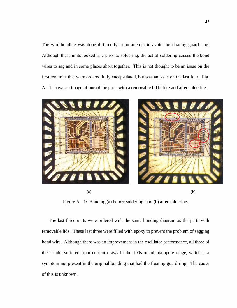
43
The wire-bonding was done differently in an attempt to avoid the floating guard ring.
Although these units looked fine prior to soldering, the act of soldering caused the bond
wires to sag and in some places short together. This is not thought to be an issue on the
first ten units that were ordered fully encapsulated, but was an issue on the last four. Fig.
A - 1 shows an image of one of the parts with a removable lid before and after soldering.
(a) (b)
Figure A - 1: Bonding (a) before soldering, and (b) after soldering.
The last three units were ordered with the same bonding diagram as the parts with
removable lids. These last three were filled with epoxy to prevent the problem of sagging
bond wire. Although there was an improvement in the oscillator performance, all three of
these units suffered from current draws in the 100s of microampere range, which is a
symptom not present in the original bonding that had the floating guard ring. The cause
of this is unknown.

44
APPENDIX C: DESIGN CONSIDERATIONS FOR LOW-POWER CONVERTER OPERATION
Minimizing losses requires careful design of each block within the overall design.
The losses in any DC-DC converter can be grouped into three main categories: (1)
conduction losses; (2) switching losses; and (3) quiescent losses. Conduction losses
occur when current passes through a non-zero resistance. The non-zero resistance of the
switches that make up the boost converters and the resistance of the inductor are the
primary culprits for conduction losses. Switching losses are the losses that occur when a
capacitance is charged and discharged. This occurs while the gate capacitance of the
switches or any digital circuitry is charged and discharged when the transistors turn on
and off. Finally, quiescent losses consist of the quiescent power of all devices. In high
power DC-DC converters, the current through the converter can become quite large,
making conduction losses dominant. As a result, switching and quiescent losses may be
negligible. Low power designs do not have this luxury. As power decreases, so too does
the current that makes up conduction losses. As a result switching losses and quiescent
losses become significant and in some cases, the dominant form of losses.
To reduce switching losses, a pulse counting scheme is implemented to reduce the
necessary clock frequency. Once the clock frequency is known, a detailed analysis can
be performed to optimize switch sizes and reduce the sum of conduction and switching
losses [18]. Optimizing quiescent losses is more difficult and must be performed on each
block by choosing topologies that minimize quiescent current.
45
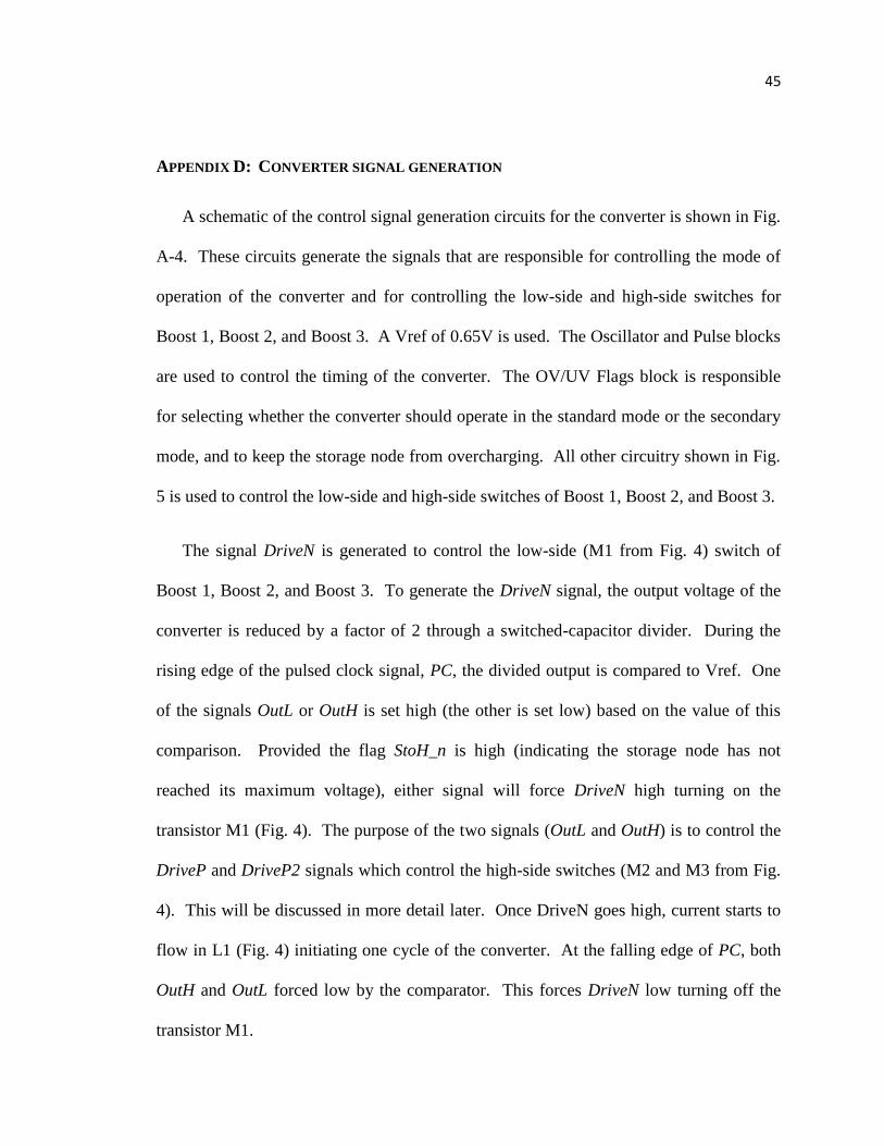
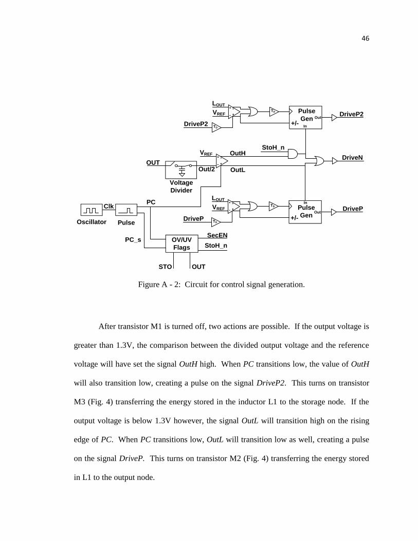
APPENDIX D: CONVERTER SIGNAL GENERATION
A schematic of the control signal generation circuits for the converter is shown in Fig.
A-4. These circuits generate the signals that are responsible for controlling the mode of
operation of the converter and for controlling the low-side and high-side switches for
Boost 1, Boost 2, and Boost 3. A Vref of 0.65V is used. The Oscillator and Pulse blocks
are used to control the timing of the converter. The OV/UV Flags block is responsible
for selecting whether the converter should operate in the standard mode or the secondary
mode, and to keep the storage node from overcharging. All other circuitry shown in Fig.
5 is used to control the low-side and high-side switches of Boost 1, Boost 2, and Boost 3.
The signal DriveN is generated to control the low-side (M1 from Fig. 4) switch of
Boost 1, Boost 2, and Boost 3. To generate the DriveN signal, the output voltage of the
converter is reduced by a factor of 2 through a switched-capacitor divider. During the
rising edge of the pulsed clock signal, PC, the divided output is compared to Vref. One
of the signals OutL or OutH is set high (the other is set low) based on the value of this
comparison. Provided the flag StoH_n is high (indicating the storage node has not
reached its maximum voltage), either signal will force DriveN high turning on the
transistor M1 (Fig. 4). The purpose of the two signals (OutL and OutH) is to control the
DriveP and DriveP2 signals which control the high-side switches (M2 and M3 from Fig.
4). This will be discussed in more detail later. Once DriveN goes high, current starts to
flow in L1 (Fig. 4) initiating one cycle of the converter. At the falling edge of PC, both
OutH and OutL forced low by the comparator. This forces DriveN low turning off the
transistor M1.
46
VREF
Out/2OUT
PC
OutH
OutL
Voltage
Divider
Oscillator Pulse
StoH_n
TDDriveP2
LOUT
VREFTD
+/-
Pulse
Gen
DriveN
DriveP2
In
Out
TDDriveP
LOUT
VREFTD
+/-
Pulse
GenDriveP
In
Out
OV/UV
Flags
PC_sSecEN
StoH_n
STO OUT
Clk
Figure A - 2: Circuit for control signal generation.
After transistor M1 is turned off, two actions are possible. If the output voltage is
greater than 1.3V, the comparison between the divided output voltage and the reference
voltage will have set the signal OutH high. When PC transitions low, the value of OutH
will also transition low, creating a pulse on the signal DriveP2. This turns on transistor
M3 (Fig. 4) transferring the energy stored in the inductor L1 to the storage node. If the
output voltage is below 1.3V however, the signal OutL will transition high on the rising
edge of PC. When PC transitions low, OutL will transition low as well, creating a pulse
on the signal DriveP. This turns on transistor M2 (Fig. 4) transferring the energy stored
in L1 to the output node.
47
For high efficiency, it is necessary for the PMOS switch (M2 or M3) to remain on
just long enough that the current in the inductor falls to zero. If the PMOS switch turns
off too early, the current in the inductor will still be positive and will be forced to flow
through the body diodes in transistors M2 or M3 in order to reach the output or storage
node, respectively. This causes considerable losses reducing efficiency. If the PMOS
switch is instead on for too long, the current in the inductor will become negative and
will discharge the output or storage node.
The required ratio between on-time of the PMOS switches, , and the on-time of the
NMOS switch, , was shown in [3] and [18] to be:
1
is set by the pulse counting block and is equal to the time of one clock pulse. Since
the clock operates at a fixed frequency, is fixed. VOUT is also fixed since the control
loop regulates the output voltage to 1.3V. The value VTEG however is temperature
dependent and therefore cannot be assumed. As a result it is necessary to have a system
which can automatically adjust the value of when necessary. A “zero-current
switching” (ZCS) control loop has previously been proposed and implemented [3, 18]. In
these designs, the voltage at LOUT (Fig. 4) is measured shortly after the PMOS switches
open to determine the correct value of . If the voltage at LOUT is high shortly after the
1 The equation given is for Boost 1 which transfers energy between the TEG and the
output. For Boost 2 the equation is the same except that VOUT is replaced with VSTO since
Boost 2 is used to transfer energy from the TEG to the storage node instead.

48
PMOS switch is opened, is too short and must be increased. If the value at LOUT is
low shortly after the PMOS switch is opened, is too long and must be decreased. As
seen in Fig. 5, the voltage at LOUT is compared to the 0.65V reference shortly after either
of the PMOS switches opens. This value is then used to increment or decrement the
length of the pulse generated by the pulse generation blocks.
49
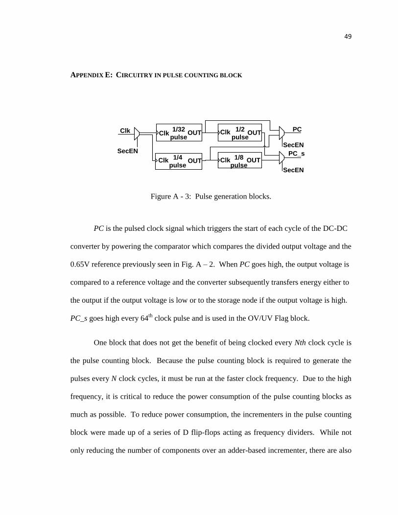
APPENDIX E: CIRCUITRY IN PULSE COUNTING BLOCK
Clk OUT Clk OUT
Clk OUT Clk OUT
1/32
pulse
1/2
pulse
1/4
pulse
1/8
pulse
PC
PC_s
SecEN
Clk
SecEN
SecEN
Figure A - 3: Pulse generation blocks.
PC is the pulsed clock signal which triggers the start of each cycle of the DC-DC
converter by powering the comparator which compares the divided output voltage and the
0.65V reference previously seen in Fig. A – 2. When PC goes high, the output voltage is
compared to a reference voltage and the converter subsequently transfers energy either to
the output if the output voltage is low or to the storage node if the output voltage is high.
PC_s goes high every 64th
clock pulse and is used in the OV/UV Flag block.
One block that does not get the benefit of being clocked every Nth clock cycle is
the pulse counting block. Because the pulse counting block is required to generate the
pulses every N clock cycles, it must be run at the faster clock frequency. Due to the high
frequency, it is critical to reduce the power consumption of the pulse counting blocks as
much as possible. To reduce power consumption, the incrementers in the pulse counting
block were made up of a series of D flip-flops acting as frequency dividers. While not
only reducing the number of components over an adder-based incrementer, there are also
50
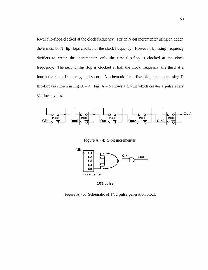
fewer flip-flops clocked at the clock frequency. For an N-bit incrementer using an adder,
there must be N flip-flops clocked at the clock frequency. However, by using frequency
dividers to create the incrementer, only the first flip-flop is clocked at the clock
frequency. The second flip flop is clocked at half the clock frequency, the third at a
fourth the clock frequency, and so on. A schematic for a five bit incrementer using D
flip-flops is shown in Fig. A – 4. Fig. A – 5 shows a circuit which creates a pulse every
32 clock cycles.
DFFD Q
QDFFD Q
QDFFD Q
QDFFD Q
QClk Out0 Out1 Out2 Out3DFFD Q
Q
Out4
Figure A - 4: 5-bit incrementer.
S1
S2
S3
S4
S5
Clk
Clk Out
Incrementer
1/32 pulse
Figure A - 5: Schematic of 1/32 pulse generation block
51
APPENDIX F: FLAG GENERATION CIRCUITRY
Φ1
Φ1
Φ2
Φ2
1pF1pF
STO/2STO
TD
OUT
SecEN
Ref
R1
R2
PC_s
SecEN_nS Q
R
S Q
R
OutH
TEGOUT
STO
TD
DFFD Q
Ref
STO/2 StoH
PC
StoH_n
Figure A - 6: Flag generation blocks.
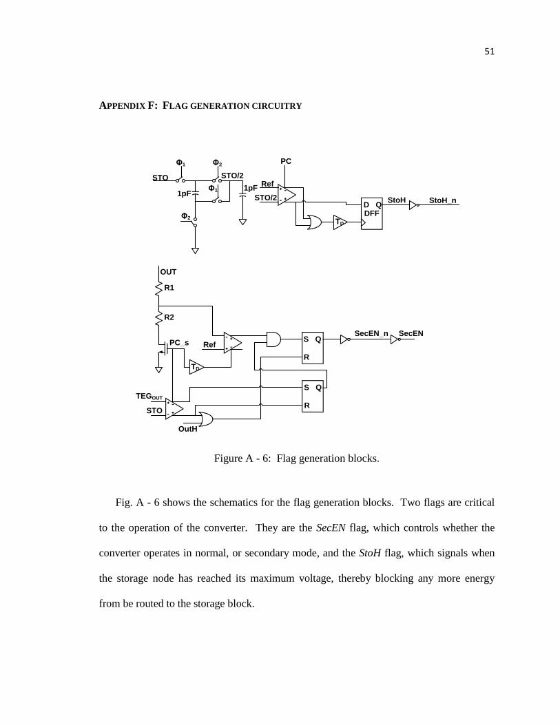
Fig. A - 6 shows the schematics for the flag generation blocks. Two flags are critical
to the operation of the converter. They are the SecEN flag, which controls whether the
converter operates in normal, or secondary mode, and the StoH flag, which signals when
the storage node has reached its maximum voltage, thereby blocking any more energy
from be routed to the storage block.
52
The StoH block is simple. A switched capacitor DC-DC converter is used to divide
the voltage at the storage node by 2. This voltage is then compared with the 0.65V
reference. When the storage node is above 1.3 V (the same voltage as the output node) the
StoH flag is set, and no more energy will be transferred to the storage node until it is no
longer above 1.3V.
The SecEN flag is more complex. A voltage divider is used to generate a fraction
of the output voltage. Because the desired ratio of 0.52*Vout is not easily obtainable
using a switched-capacitor divider, a resistive divider is used instead. These resistors are
external and adjustable by the user. In order to decrease quiescent losses, the duty cycle of
the divider is limited by only powering the divider when PC_s is high. This occurs once
every 64 clock pulses. The output of the voltage divider is then compared with the
reference node, which is typically half of the output voltage. A reference node voltage
greater than 0.52*VOUT signifies that the output voltage has dropped too much and energy
must be pumped from the storage node to compensate. If VSTO is greater than VTEG and
.52*VOUT falls below the reference voltage, the flag, SecEN is set. This flag will then
remain high until the signal OutH goes high which signifies the output voltage is at least
1.3V. At this time, the flag SecEN is set low, and the converter functions in standard
mode again. Fig. A - 7. shows a simulation of the output and storage nodes when
secondary mode is enabled. At the point secondary node is enabled, energy is routed from
the storage node, causing its voltage to decrease, to the output node, causing the output
voltage to increase. Energy is routed from the storage node to the output node until the
53
output node voltage reaches the necessary level, and then the secondary mode is disabled,
whereby the converter returns to normal operation.
Figure A - 7: Simulation of secondary mode.
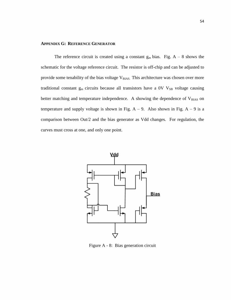
54
APPENDIX G: REFERENCE GENERATOR
The reference circuit is created using a constant gm bias. Fig. A – 8 shows the
schematic for the voltage reference circuit. The resistor is off-chip and can be adjusted to
provide some tenability of the bias voltage VBIAS. This architecture was chosen over more
traditional constant gm circuits because all transistors have a 0V VSB voltage causing
better matching and temperature independence. A showing the dependence of VBIAS on
temperature and supply voltage is shown in Fig. A – 9. Also shown in Fig. A – 9 is a
comparison between Out/2 and the bias generator as Vdd changes. For regulation, the
curves must cross at one, and only one point.
Figure A - 8: Bias generation circuit
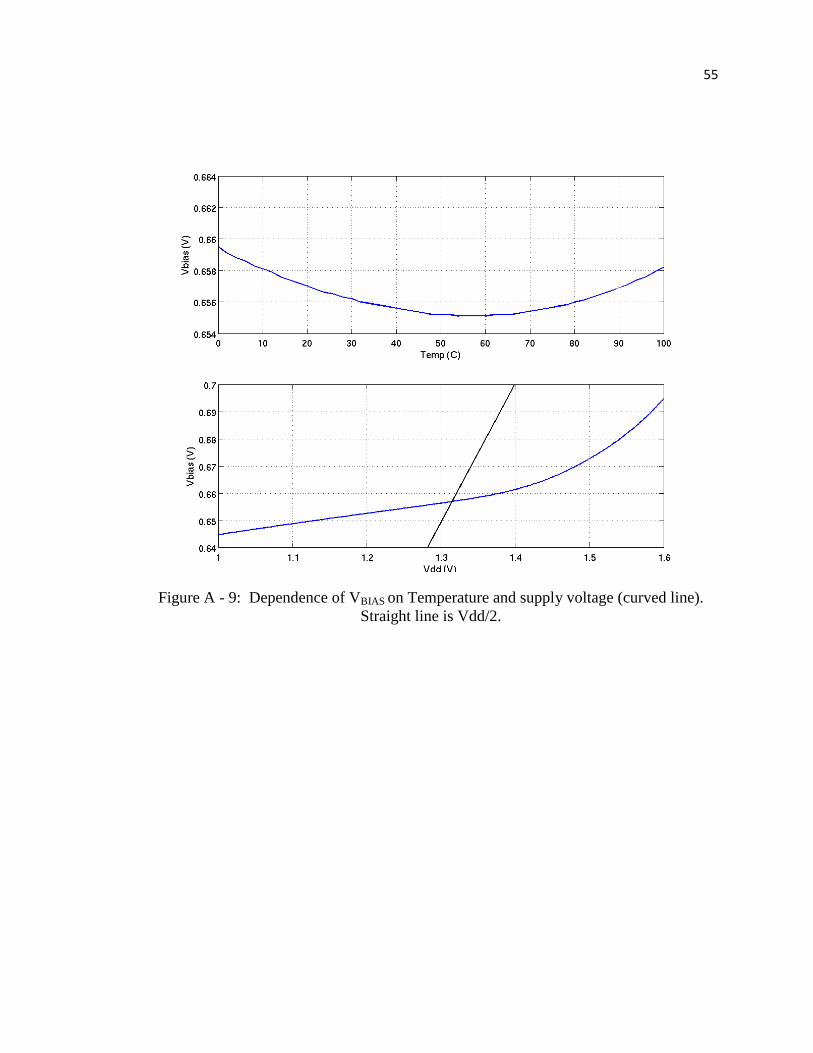
55
Figure A - 9: Dependence of VBIAS on Temperature and supply voltage (curved line).
Straight line is Vdd/2.
56
APPENDIX H: OSCILLATOR BIASING
Typically the current source in a current-starved ring oscillator is generated by
creating a bias voltage and applying the bias voltage to the gate of a MOSFET.
Generating this bias voltage can be problematic for low power designs. Resistive voltage
dividers consume quiescent current at all times. A 10MΩ resistor divider consumes
nearly 170 nW at an output voltage of 1.3V. For ultra-low power designs this much
power cannot be wasted. Instead a switched-capacitor divider was used. The switched
capacitor divider consumes only 9 nW of power in simulations. A schematic of the
switched capacitor divider is shown in Fig. A – 10. For testing purposes, the current
sources in the oscillator are adjustable using four bits of binary weighting. This can be
used to adjust the frequency of the oscillator. Fig. A – 11 shows a more detailed
schematic of the oscillator than what was previously shown in Fig. 8.
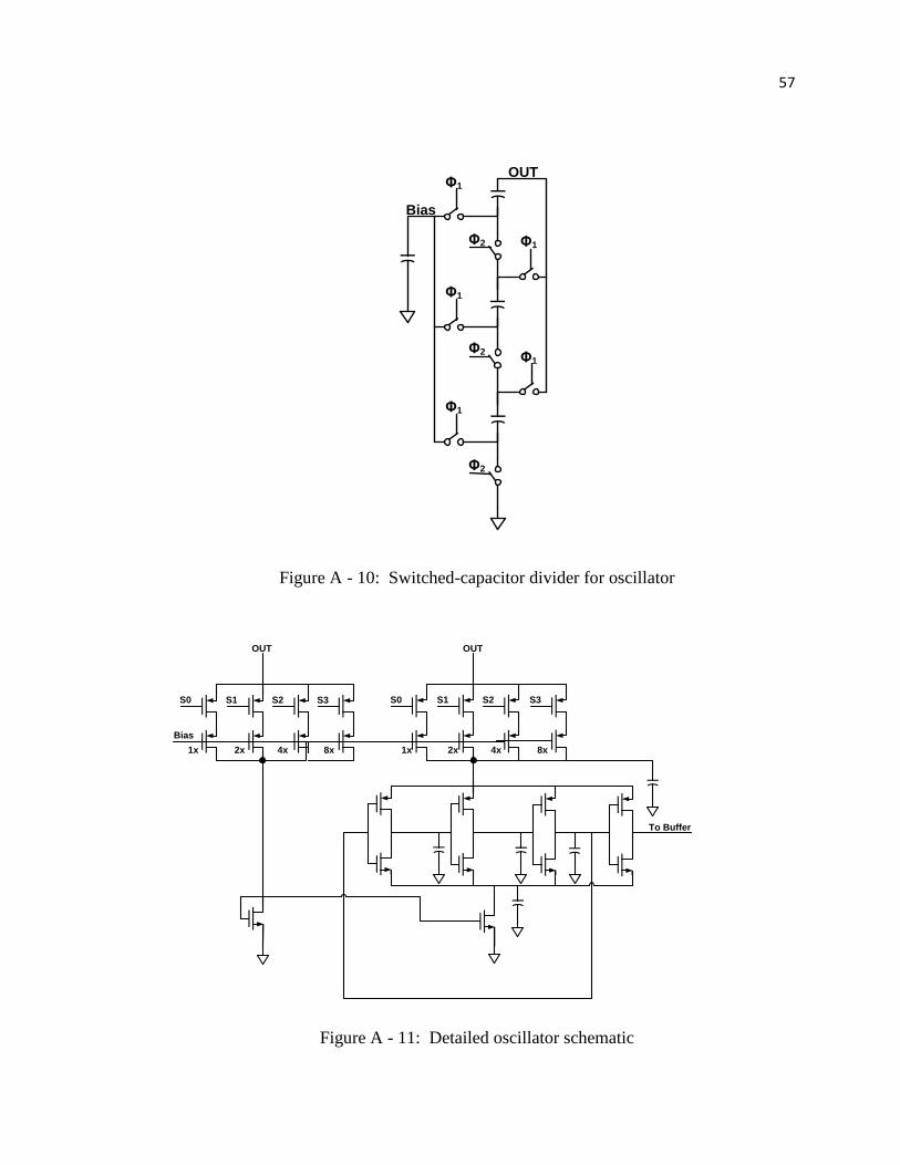
57
Φ2
Φ2
Φ2
Φ1
Φ1
Φ1
Φ1
Φ1
OUT
Bias
Figure A - 10: Switched-capacitor divider for oscillator
S0
OUTOUT
S1 S2 S0 S1 S2
Bias
S3 S3
To Buffer
1x 2x 4x 8x 1x 2x 4x 8x
Figure A - 11: Detailed oscillator schematic