AN-679 APPLICATION NOTE - Analog Devices · AN-679 APPLICATION NOTE ... NOTES 1The current ranges...
20
AN-679 APPLICATION NOTE One Technology Way • P.O. Box 9106 • Norwood, MA 02062-9106 • Tel T T : 781/329-4700 • Fax: 781/326-8703 • www.analog.com INTRODUCTION This application note describes a high accuracy, low cost, single-phase power meter based on the ADE7757. The meter is designed for use in single-phase, 2-wire distribution systems. The design can be adapted to suit specific regional requirements, e.g., in the U.S., power is usually distributed for residential customers as single- phase, 3-wire. The ADE7757 is a low cost, single-chip solution for electrical energy measurement. The ADE7757 is a highly integrated system comprised of two ADCs, a reference circuit, and a fixed DSP function for the calculation of real power. A highly stable oscillator is integrated into the design to provide the necessary clock for the IC. The ADE7757 includes direct drive capability for electrome- chanical counters and a high frequency pulse output for both calibration and system communication. This application note should be used in conjunction with the ADE7757 Data Sheet. The data sheet provides detailed information on the functionality of the ADE7757 and will be referenced several times in this application note. DESIGN GOALS The International Standard IEC 61036 (2000-09), Alter- nating Current Static Watt-Hour Meters for Active Energy (Classes 1 and 2), was used as the primary specification for this design. For readers more familiar with the ANSI C12.16 specification, see the ANSI C12.16 and IEC 61036 section at the end of this application note for a com- parison of the two standards. The section explains the key IEC 61036 specifications in terms of their ANSI equivalents. A Low Cost Watt-Hour Energy Meter Based on the ADE7757 by Stephen T. English The ADE7757 board design greatly exceeds this basic specification for many of the accuracy requirements, e.g., accuracy at unity power factor and at a low power factor (PF = ±0.5). In addition, the dynamic range per- formance of the meter has been extended to 400. The IEC 61036 standard specifies accuracy over a range of 5% Ib to I MAX (see Table I). Typical values for I MAX are 400% to 600% of Ib. Table I. Accuracy Requirements Percentage Error Limits 3 Current Value 1 PF 2 Class 1 Class 2 0.05 lb < I < 0.1 lb 1 ±1.5% ±2.5% 0.1 lb < I < I MAX 1 ±1.0% ±2.0% 0.1 lb < I < 0.2 lb 0.5 Lag ±1.5% ±2.5% 0.8 Lead ±1.5% 0.2 lb < I < I MAX 0.5 Lag ±1.0% ±2.0% 0.8 Lead ±1.0% NOTES 1 The current ranges for specified accuracy shown in Table I are expressed in terms of the basic current (Ib). The basic current is defined in IEC 61036 (2000–09) Section 3.5.1.1 as the value of current in accordance with which the relevant performance of a direct connection meter is fixed. I MAX is the maximum current at which accuracy is maintained. 2 Power factor (PF) in Table I relates the phase relationship between the fundamental voltage (45 Hz to 65 Hz) and current waveforms. PF, in this case, can be simply defined as PF = cos(), where is the phase angle between pure sinusoidal current and voltage. 3 Class index is defined in IEC 61036 (2000–09) Section 3.5.5, Page 27, as the limits of the permissible percentage error. The percentage error is defined as Percentage Error Energy Registered by Meter – True Energy True Energy 100% = × REV. A
Transcript of AN-679 APPLICATION NOTE - Analog Devices · AN-679 APPLICATION NOTE ... NOTES 1The current ranges...
AN-679APPLICATION NOTE
One Technology Way • P.O. Box 9106 • Norwood, MA 02062-9106 • TelTelT : 781/329-4700 • Fax: 781/326-8703 • www.analog.com
INTRODUCTIONThis application note describes a high accuracy, low cost, single-phase power meter based on the ADE7757. The meter is designed for use in single-phase, 2-wire distribution systems. The design can be adapted to suit specifi c regional requirements, e.g., in the U.S., power is usually distributed for residential customers as single-phase, 3-wire.
The ADE7757 is a low cost, single-chip solution for electrical energy measurement. The ADE7757 is a highly integrated system comprised of two ADCs, a reference circuit, and a fi xed DSP function for the calculation of real power. A highly stable oscillator is integrated into the design to provide the necessary clock for the IC. The ADE7757 includes direct drive capability for electrome-chanical counters and a high frequency pulse output for both calibration and system communication.
This application note should be used in conjunction with the ADE7757 Data Sheet. The data sheet provides detailed information on the functionality of the ADE7757 and will be referenced several times in this application note.
DESIGN GOALSThe International Standard IEC 61036 (2000-09), Alter-nating Current Static Watt-Hour Meters for Active Energy (Classes 1 and 2), was used as the primary specifi cation for this design. For readers more familiar with the ANSI C12.16 specifi cation, see the ANSI C12.16 and IEC 61036 section at the end of this application note for a com-parison of the two standards. The section explains the key IEC 61036 specifications in terms of their ANSI equivalents.
A Low Cost Watt-Hour Energy Meter Based on the ADE7757by Stephen T. English
The ADE7757 board design greatly exceeds this basic specifi cation for many of the accuracy requirements, e.g., accuracy at unity power factor and at a low power factor (PF = ±0.5). In addition, the dynamic range per-formance of the meter has been extended to 400. The IEC 61036 standard specifi es accuracy over a range of 5% Ib to IMAX (see Table I). Typical values for IMAX are 400% to 600% of Ib.
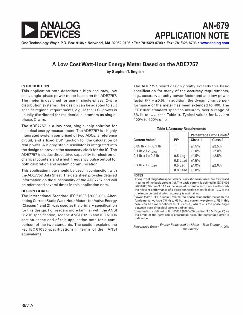
Table I. Accuracy Requirements
Percentage Error Limits3
Current Value1 PF2 Class 1 Class 2
0.05 lb < I < 0.1 lb 1 ±1.5% ±2.5%0.1 lb < I < IMAX 1 ±1.0% ±2.0%0.1 lb < I < 0.2 lb 0.5 Lag ±1.5% ±2.5% 0.8 Lead ±1.5% 0.2 lb < I < IMAX 0.5 Lag ±1.0% ±2.0% 0.8 Lead ±1.0%NOTES1The current ranges for specifi ed accuracy shown in Table I are expressed in terms of the basic current (Ib). The basic current is defi ned in IEC 61036 (2000–09) Section 3.5.1.1 as the value of current in accordance with which the relevant performance of a direct connection meter is fi xed. IMAX is the maximum current at which accuracy is maintained.
2Power factor (PF) in Table I relates the phase relationship between the fundamental voltage (45 Hz to 65 Hz) and current waveforms. PF, in this case, can be simply defi ned as PF = cos(), where is the phase angle between pure sinusoidal current and voltage.
3Class index is defi ned in IEC 61036 (2000–09) Section 3.5.5, Page 27, as the limits of the permissible percentage error. The percentage error is defi ned as
Percentage ErrorEnergy Registered by Meter – True Energy
True Energy100%= ×= ×Energy Registered by Meter= ×Energy Registered by Meter True Energy= ×True Energy
REV. A
–2–
AN-679
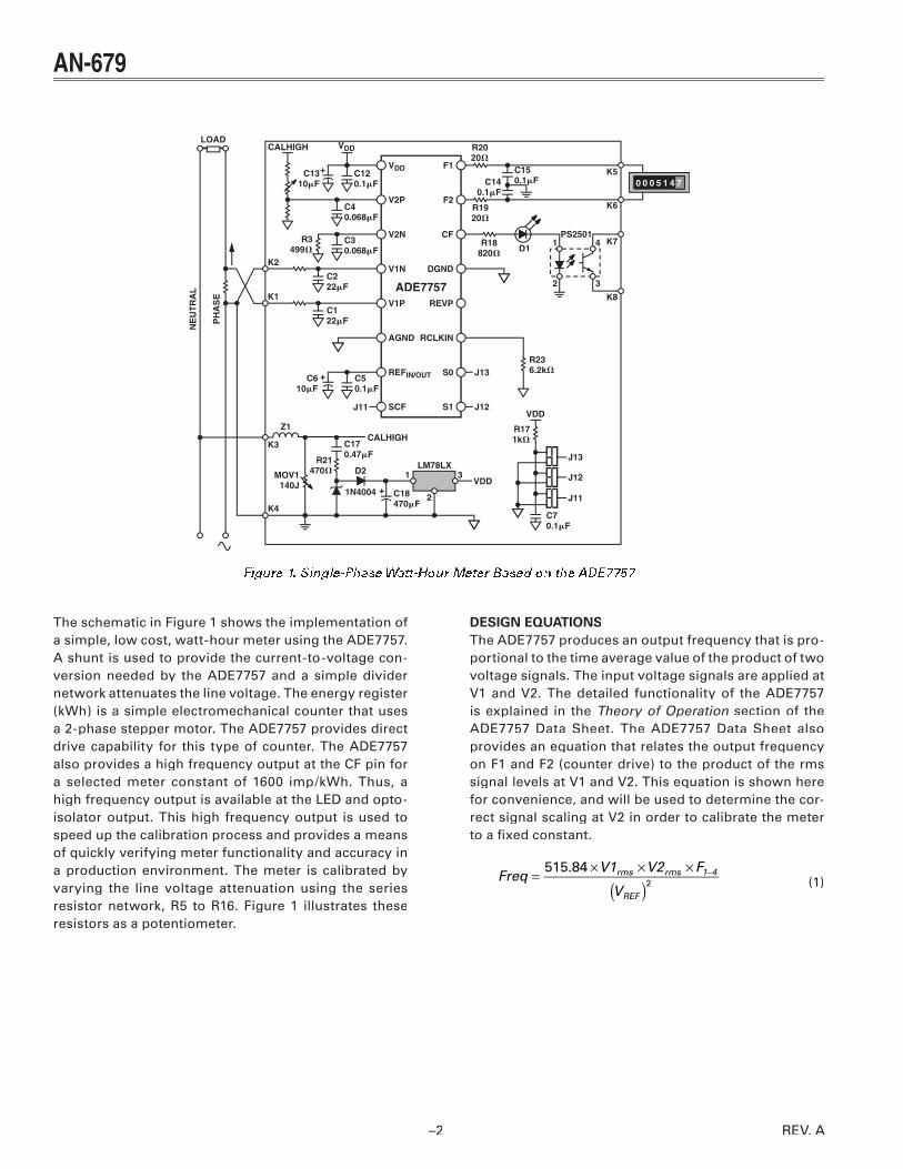
The schematic in Figure 1 shows the implementation of a simple, low cost, watt-hour meter using the ADE7757. A shunt is used to provide the current-to-voltage con-version needed by the ADE7757 and a simple divider network attenuates the line voltage. The energy register (kWh) is a simple electromechanical counter that uses a 2-phase stepper motor. The ADE7757 provides direct drive capability for this type of counter. The ADE7757 also provides a high frequency output at the CF pin for a selected meter constant of 1600 imp/kWh. Thus, a high frequency output is available at the LED and opto-isolator output. This high frequency output is used to speed up the calibration process and provides a means of quickly verifying meter functionality and accuracy in a production environment. The meter is calibrated by varying the line voltage attenuation using the series resistor network, R5 to R16. Figure 1 illustrates theseresistors as a potentiometer.
DESIGN EQUATIONSThe ADE7757 produces an output frequency that is pro-portional to the time average value of the product of two voltage signals. The input voltage signals are applied at V1 and V2. The detailed functionality of the ADE7757 is explained in the Theory of Operation section of the ADE7757 Data Sheet. The ADE7757 Data Sheet also provides an equation that relates the output frequency on F1 and F2 (counter drive) to the product of the rms signal levels at V1 and V2. This equation is shown here for convenience, and will be used to determine the cor-rect signal scaling at V2 in order to calibrate the meter to a fi xed constant.
FreqV1 V2 F
Vrms rms 1–4
REF
= × × ×
( )515.84
2
(1)
���
���
�����������
�����
�������
���
���
���
���
����
���
��
��
��
���������
���
���
������
��������
������
� �
� ���
���
��
��
��
����
����
�������
������
�����
��
��
��
��
��
������
������
�������
������
�����������
������������
�������
���������
������
�������
������
���������
���������
�����������
�����
���
�
�
�
���
��������
�������
��
������
��
������
�������
��������
������
� � � � � � �
Figure 1. Single-Phase Watt-Hour Meter Based on the ADE7757
REV. A
–3–
AN-679
The meter shown in Figure 1 is designed to operate at a line voltage of 220 V and a maximum current (IMAX) of 30 A. However, by correctly scaling the signals on Channel 1 and Channel 2, a meter operating at any line voltage and maximum current could be designed.
The four frequency options available on the ADE7757 will allow similar meters (i.e., direct counter drive) with an IMAX of up to 120 A to be designed. The basic current (Ib) for this meter is selected as 5 A and the current range for accuracy will be 2% of Ib to IMAX, or a dynamic range of 400:1 (75 mA to 30 A).
The electromechanical register (kWh) will have a constant of 100 imp/kWh, i.e., 100 impulses from the ADE7757 will be required to register 1 kWh. IEC 61036 Section 4.2.11 specifi es that electromagnetic registers have their lowest values numbered in 10 divisions, each division being subdivided into 10 parts. Therefore, a display with fi ve plus one digits is used, i.e., 10,000s, 1,000s, 100s, 10s, 1s, and 1/10s. The meter constant (for calibration and test) is selected as 1600 imp/kWh.
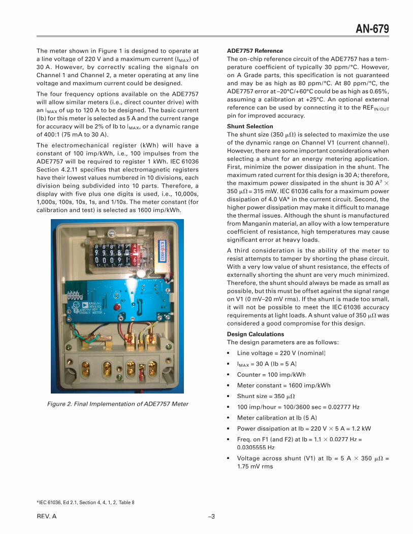
Figure 2. Final Implementation of ADE7757 Meter
ADE7757 ReferenceThe on-chip reference circuit of the ADE7757 has a tem-perature coeffi cient of typically 30 ppm/°C. However, on A Grade parts, this specifi cation is not guaranteed and may be as high as 80 ppm/°C. At 80 ppm/°C, the ADE7757 error at –20°C/+60°C could be as high as 0.65%, assuming a calibration at +25°C. An optional external reference can be used by connecting it to the REFIN/OUT
pin for improved accuracy.
Shunt SelectionThe shunt size (350 ) is selected to maximize the use of the dynamic range on Channel V1 (current channel). However, there are some important considerations when selecting a shunt for an energy metering application. First, minimize the power dissipation in the shunt. The maximum rated current for this design is 30 A; therefore, the maximum power dissipated in the shunt is 30 A2
350 = 315 mW. IEC 61036 calls for a maximum power dissipation of 4.0 VA* in the current circuit. Second, the higher power dissipation may make it diffi cult to manage the thermal issues. Although the shunt is manufactured from Manganin material, an alloy with a low temperature coeffi cient of resistance, high temperatures may cause signifi cant error at heavy loads.
A third consideration is the ability of the meter to resist attempts to tamper by shorting the phase circuit. With a very low value of shunt resistance, the effects of externally shorting the shunt are very much minimized. Therefore, the shunt should always be made as small as possible, but this must be offset against the signal range on V1 (0 mV–20 mV rms). If the shunt is made too small, it will not be possible to meet the IEC 61036 accuracy requirements at light loads. A shunt value of 350 was considered a good compromise for this design.
Design CalculationsThe design parameters are as follows:
• Line voltage = 220 V (nominal)
• IMAX = 30 A (Ib = 5 A)
• Counter = 100 imp/kWh
• Meter constant = 1600 imp/kWh
• Shunt size = 350
• 100 imp/hour = 100/3600 sec = 0.02777 Hz
• Meter calibration at Ib (5 A)
• Power dissipation at Ib = 220 V 5 A = 1.2 kW
• Freq. on F1 (and F2) at Ib = 1.1 0.0277 Hz = 0.0305555 Hz
• Voltage across shunt (V1) at Ib = 5 A 350 = 1.75 mV rms
*IEC 61036, Ed 2.1, Section 4, 4, 1, 2, Table 8
REV. A
–4–
AN-679
To select the F1–4 frequency for Equation 1, see the Selecting a Frequency for an Energy Meter Applicationsection in the ADE7757 Data Sheet. From Tables IV and V in the data sheet, it can be seen that the best choice of F1–4 frequency for a meter with IMAX = 30 A is 3.44 Hz (F2). This frequency selection is made by logic inputs S0 and S1 (see Table II in the ADE7757 Data Sheet). The CF frequency (meter constant) is selected by using the logic input SCF. The two available options are 16 F1 (1600 imp/kWh) or 32 F1 (3200 imp/kWh). For this design, 1600 imp/kWh is selected by setting SCF logic low. With a meter constant of 1600 imp/kWh and a maxi-mum current of 30 A, the maximum frequency from CF is 11.2 Hz. The only remaining unknown from Equation 1 is V2 or the signal level on Channel 2 (the voltage channel).
From Equation 1, solving for V2 gives 61.5 mV rms:V2 gives 61.5 mV rms:V2
0.0305555 Hz515.84 1.75mV
2.52= × × ×V2 F1–4
2.5 2.5 (2)
Therefore, to calibrate the meter with the line voltage, the input V2 must be attenuated to this value.V2 must be attenuated to this value.V2
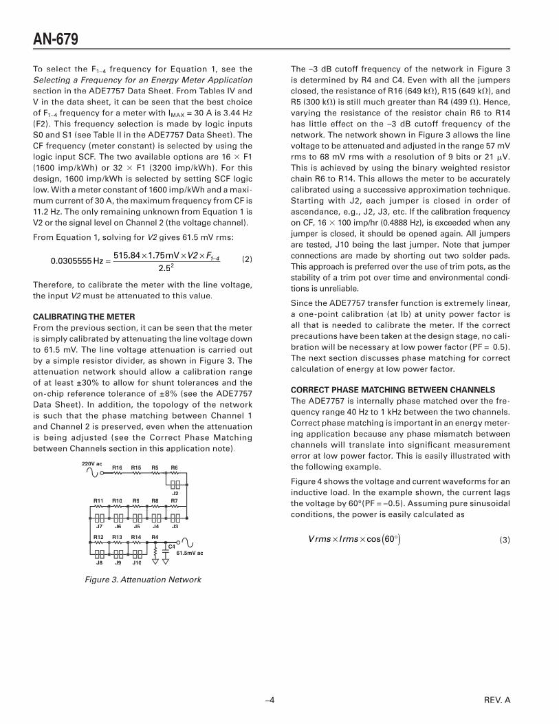
CALIBRATING THE METERFrom the previous section, it can be seen that the meter is simply calibrated by attenuating the line voltage down to 61.5 mV. The line voltage attenuation is carried out by a simple resistor divider, as shown in Figure 3. The attenuation network should allow a calibration range of at least ±30% to allow for shunt tolerances and the on-chip reference tolerance of ±8% (see the ADE7757 Data Sheet). In addition, the topology of the network is such that the phase matching between Channel 1 and Channel 2 is preserved, even when the attenuation is being adjusted (see the Correct Phase Matching between Channels section in this application note).
R16 R15 R5 R6
R10R11 R9 R8
R13R12 R14 R4
J6J7 J5
J9J8 J10
J4 J3
C461.5mV ac
220V ac
R7J2
Figure 3. Attenuation Network
The –3 dB cutoff frequency of the network in Figure 3 is determined by R4 and C4. Even with all the jumpers closed, the resistance of R16 (649 k), R15 (649 k), and R5 (300 k) is still much greater than R4 (499 ). Hence, varying the resistance of the resistor chain R6 to R14 has little effect on the –3 dB cutoff frequency of the network. The network shown in Figure 3 allows the line voltage to be attenuated and adjusted in the range 57 mV rms to 68 mV rms with a resolution of 9 bits or 21 V. This is achieved by using the binary weighted resistor chain R6 to R14. This allows the meter to be accurately calibrated using a successive approximation technique. Starting with J2, each jumper is closed in order of ascendance, e.g., J2, J3, etc. If the calibration frequency on CF, 16 100 imp/hr (0.4888 Hz), is exceeded when any jumper is closed, it should be opened again. All jumpers are tested, J10 being the last jumper. Note that jumper connections are made by shorting out two solder pads. This approach is preferred over the use of trim pots, as the stability of a trim pot over time and environmental condi-tions is unreliable.
Since the ADE7757 transfer function is extremely linear, a one-point calibration (at Ib) at unity power factor is all that is needed to calibrate the meter. If the correct precautions have been taken at the design stage, no cali-bration will be necessary at low power factor (PF = 0.5). The next section discusses phase matching for correct calculation of energy at low power factor.
CORRECT PHASE MATCHING BETWEEN CHANNELSThe ADE7757 is internally phase matched over the fre-quency range 40 Hz to 1 kHz between the two channels. Correct phase matching is important in an energy meter-ing application because any phase mismatch between channels will translate into signifi cant measurement error at low power factor. This is easily illustrated with the following example.
Figure 4 shows the voltage and current waveforms for an inductive load. In the example shown, the current lags the voltage by 60°(PF = –0.5). Assuming pure sinusoidal conditions, the power is easily calculated as
Vrms Irms× × °( )cos 60 (3)
REV. A
–5–
AN-679
If, however, a phase error (e) is introduced externally to the ADE7757, e.g., in the antialias fi lters, the error is calculated as
cos – cos / cos 100%eδ δ φ δ°( ) ° +( )[ ] °( ) ×
(4)
where is the phase angle between voltage and cur-rent and e is the external phase error (see Note 3 in Table I). With a phase error of 0.2°, for example, the error at PF = 0.5 (60°) is calculated to be 0.6%. As this example dem-onstrates, even a very small phase error will produce a large measurement error at low power factor.
���
������������������������������
������������������������������
�������������������������
�������������������������
�������
�������
������
��������
�� ��
�������
�����������������
Figure 4. Voltage and Current (Inductive Load)
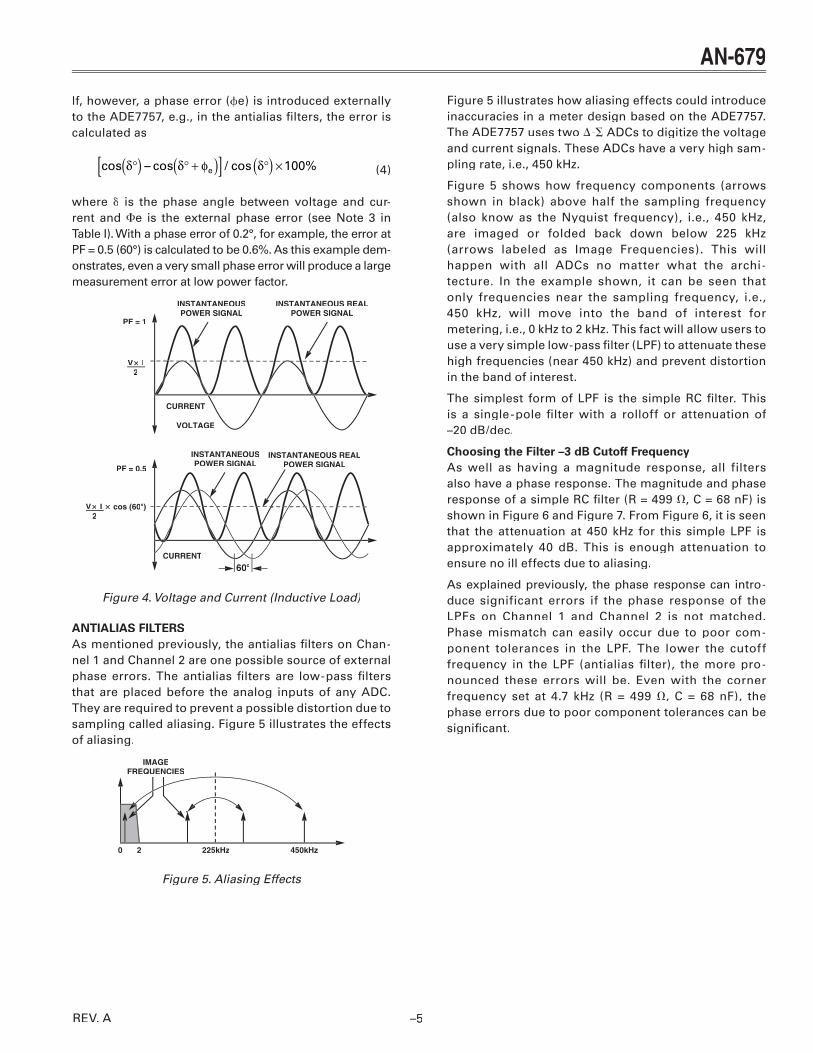
ANTIALIAS FILTERSAs mentioned previously, the antialias fi lters on Chan-nel 1 and Channel 2 are one possible source of external phase errors. The antialias fi lters are low-pass fi lters that are placed before the analog inputs of any ADC. They are required to prevent a possible distortion due to sampling called aliasing. Figure 5 illustrates the effects of aliasing.
0 2 225kHz
IMAGEFREQUENCIES
450kHz
Figure 5. Aliasing Effects
Figure 5 illustrates how aliasing effects could introduce inaccuracies in a meter design based on the ADE7757. The ADE7757 uses two - ADCs to digitize the voltage and current signals. These ADCs have a very high sam-pling rate, i.e., 450 kHz.
Figure 5 shows how frequency components (arrows shown in black) above half the sampling frequency (also know as the Nyquist frequency), i.e., 450 kHz, are imaged or folded back down below 225 kHz (arrows labeled as Image Frequencies). This will happen with all ADCs no matter what the archi-tecture. In the example shown, it can be seen that only frequencies near the sampling frequency, i.e., 450 kHz, will move into the band of interest for metering, i.e., 0 kHz to 2 kHz. This fact will allow users to use a very simple low-pass fi lter (LPF) to attenuate these high frequencies (near 450 kHz) and prevent distortion in the band of interest.
The simplest form of LPF is the simple RC fi lter. This is a single-pole fi lter with a rolloff or attenuation of –20 dB/dec.
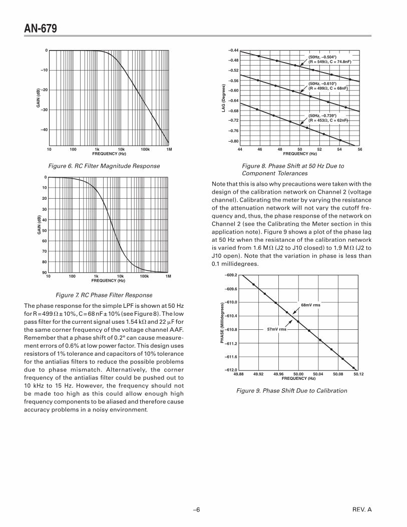
Choosing the Filter –3 dB Cutoff FrequencyAs well as having a magnitude response, all filters also have a phase response. The magnitude and phase response of a simple RC fi lter (R = 499 , C = 68 nF) is shown in Figure 6 and Figure 7. From Figure 6, it is seen that the attenuation at 450 kHz for this simple LPF is approximately 40 dB. This is enough attenuation to ensure no ill effects due to aliasing.
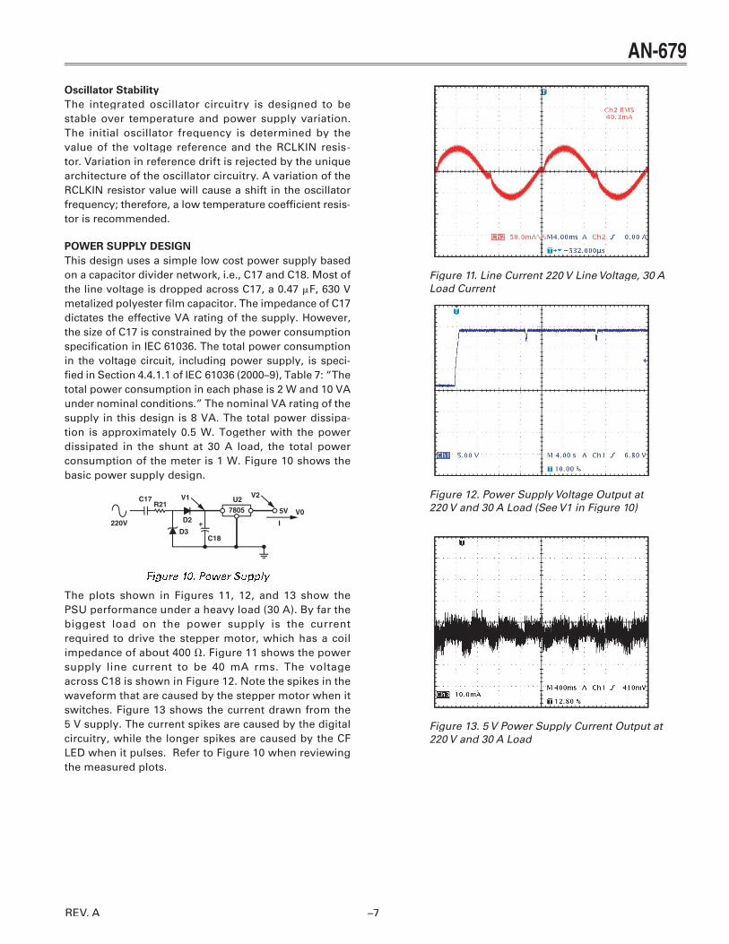
As explained previously, the phase response can intro-duce significant errors if the phase response of the LPFs on Channel 1 and Channel 2 is not matched. Phase mismatch can easily occur due to poor com-ponent tolerances in the LPF. The lower the cutoff frequency in the LPF (antialias fi lter), the more pro-nounced these errors will be. Even with the corner frequency set at 4.7 kHz (R = 499 , C = 68 nF), the phase errors due to poor component tolerances can be signifi cant.
REV. A
–6–
AN-679
��������������
�
���
���
���
���
�� ����� ��� ���� ��
��
����
��
�
Figure 6. RC Filter Magnitude Response
��������������
�
��
��
��
��
��
��
��
��
��
�� ����� ��� ���� ��
��
����
��
�
Figure 7. RC Phase Filter Response
The phase response for the simple LPF is shown at 50 Hz for R = 499 ± 10%, C = 68 nF ± 10% (see Figure 8). The low pass fi lter for the current signal uses 1.54 k and 22 F for the same corner frequency of the voltage channel AAF. Remember that a phase shift of 0.2° can cause measure-ment errors of 0.6% at low power factor. This design uses resistors of 1% tolerance and capacitors of 10% tolerance for the antialias fi lters to reduce the possible problems due to phase mismatch. Alternatively, the corner frequency of the antialias fi lter could be pushed out to 10 kHz to 15 Hz. However, the frequency should not be made too high as this could allow enough high frequency components to be aliased and therefore cause accuracy problems in a noisy environment.
��������������
�����
�����
�����
�����
�����
�����
�����
�����
�����
�����
�� ���� �� �� �� ��
�������������
�����������������������������������
�����������������������������������
�������������������������������������
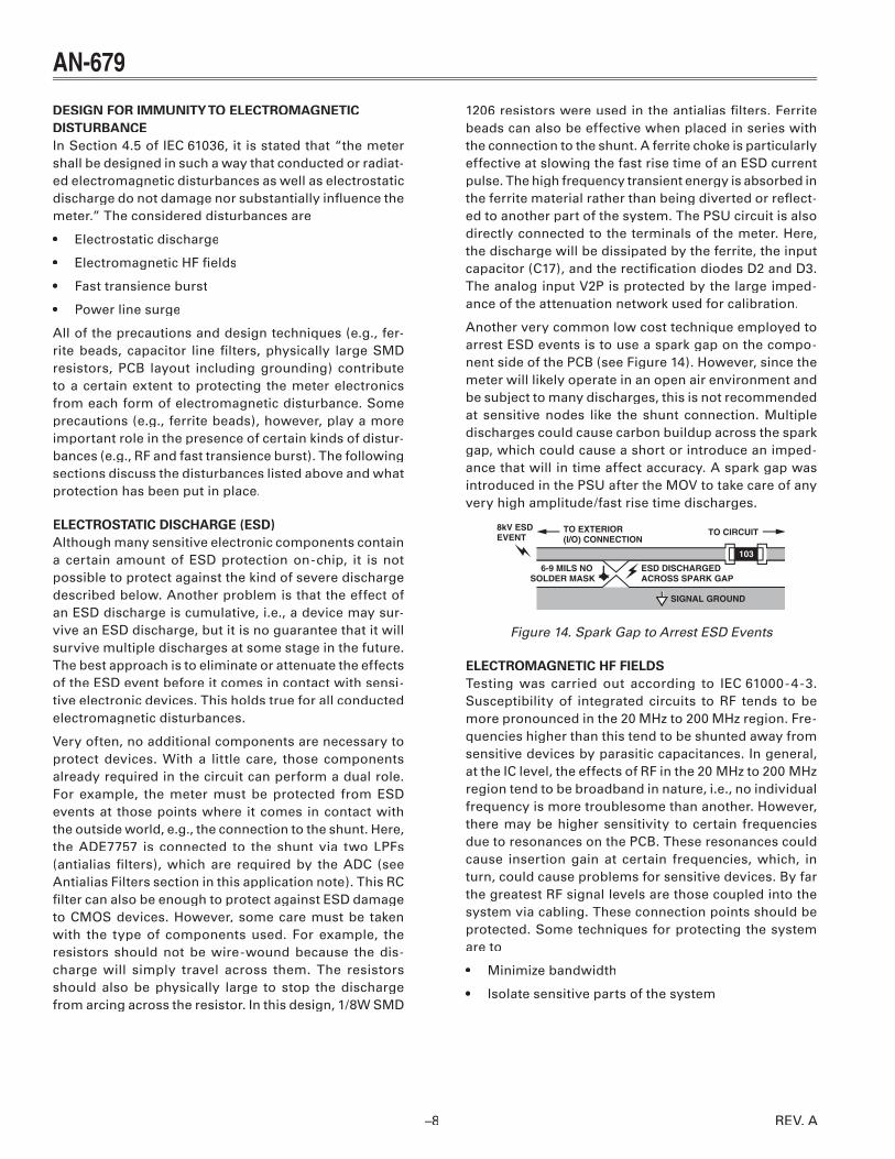
Figure 8. Phase Shift at 50 Hz Due to Component Tolerances
Note that this is also why precautions were taken with the design of the calibration network on Channel 2 (voltage channel). Calibrating the meter by varying the resistance of the attenuation network will not vary the cutoff fre-quency and, thus, the phase response of the network on Channel 2 (see the Calibrating the Meter section in this application note). Figure 9 shows a plot of the phase lag at 50 Hz when the resistance of the calibration network is varied from 1.6 M (J2 to J10 closed) to 1.9 M (J2 to J10 open). Note that the variation in phase is less than 0.1 millidegrees.
��������������
������
������
������
������
������
������
������
����������� ���������� ����� ����� ����� �����
��
��
���
����
����
����
�
��������
��������
Figure 9. Phase Shift Due to Calibration
REV. A
–7–
AN-679
Oscillator StabilityThe integrated oscillator circuitry is designed to be stable over temperature and power supply variation. The initial oscillator frequency is determined by the value of the voltage reference and the RCLKIN resis-tor. Variation in reference drift is rejected by the unique architecture of the oscillator circuitry. A variation of the RCLKIN resistor value will cause a shift in the oscillator frequency; therefore, a low temperature coeffi cient resis-tor is recommended.
POWER SUPPLY DESIGNThis design uses a simple low cost power supply based on a capacitor divider network, i.e., C17 and C18. Most of the line voltage is dropped across C17, a 0.47 F, 630 V metalized polyester fi lm capacitor. The impedance of C17 dictates the effective VA rating of the supply. However, the size of C17 is constrained by the power consumption specifi cation in IEC 61036. The total power consumption in the voltage circuit, including power supply, is speci-fi ed in Section 4.4.1.1 of IEC 61036 (2000–9), Table 7: “The total power consumption in each phase is 2 W and 10 VA under nominal conditions.” The nominal VA rating of the supply in this design is 8 VA. The total power dissipa-tion is approximately 0.5 W. Together with the power dissipated in the shunt at 30 A load, the total power consumption of the meter is 1 W. Figure 10 shows the basic power supply design.
����
���
���
��
�
��
����
��
��
�������
��
�
Figure 10. Power Supply
The plots shown in Figures 11, 12, and 13 show the PSU performance under a heavy load (30 A). By far the biggest load on the power supply is the current required to drive the stepper motor, which has a coil impedance of about 400 . Figure 11 shows the power supply line current to be 40 mA rms. The voltage across C18 is shown in Figure 12. Note the spikes in the waveform that are caused by the stepper motor when it switches. Figure 13 shows the current drawn from the 5 V supply. The current spikes are caused by the digital circuitry, while the longer spikes are caused by the CF LED when it pulses. Refer to Figure 10 when reviewing the measured plots.
Figure 11. Line Current 220 V Line Voltage, 30 A Load Current
Figure 12. Power Supply Voltage Output at 220 V and 30 A Load (See V1 in Figure 10)
Figure 13. 5 V Power Supply Current Output at 220 V and 30 A Load
REV. A
–8–
AN-679
DESIGN FOR IMMUNITY TO ELECTROMAGNETIC DISTURBANCEIn Section 4.5 of IEC 61036, it is stated that “the meter shall be designed in such a way that conducted or radiat-ed electromagnetic disturbances as well as electrostatic discharge do not damage nor substantially infl uence the meter.” The considered disturbances are
• Electrostatic discharge
• Electromagnetic HF fi elds
• Fast transience burst
• Power line surge
All of the precautions and design techniques (e.g., fer-rite beads, capacitor line fi lters, physically large SMD resistors, PCB layout including grounding) contribute to a certain extent to protecting the meter electronics from each form of electromagnetic disturbance. Some precautions (e.g., ferrite beads), however, play a more important role in the presence of certain kinds of distur-bances (e.g., RF and fast transience burst). The following sections discuss the disturbances listed above and what protection has been put in place.
ELECTROSTATIC DISCHARGE (ESD)Although many sensitive electronic components contain a certain amount of ESD protection on-chip, it is not possible to protect against the kind of severe discharge described below. Another problem is that the effect of an ESD discharge is cumulative, i.e., a device may sur-vive an ESD discharge, but it is no guarantee that it will survive multiple discharges at some stage in the future. The best approach is to eliminate or attenuate the effects of the ESD event before it comes in contact with sensi-tive electronic devices. This holds true for all conducted electromagnetic disturbances.
Very often, no additional components are necessary to protect devices. With a little care, those components already required in the circuit can perform a dual role. For example, the meter must be protected from ESD events at those points where it comes in contact with the outside world, e.g., the connection to the shunt. Here, the ADE7757 is connected to the shunt via two LPFs (antialias fi lters), which are required by the ADC (see Antialias Filters section in this application note). This RC fi lter can also be enough to protect against ESD damage to CMOS devices. However, some care must be taken with the type of components used. For example, the resistors should not be wire-wound because the dis-charge will simply travel across them. The resistors should also be physically large to stop the discharge from arcing across the resistor. In this design, 1/8W SMD
1206 resistors were used in the antialias fi lters. Ferrite beads can also be effective when placed in series with the connection to the shunt. A ferrite choke is particularly effective at slowing the fast rise time of an ESD current pulse. The high frequency transient energy is absorbed in the ferrite material rather than being diverted or refl ect-ed to another part of the system. The PSU circuit is also directly connected to the terminals of the meter. Here, the discharge will be dissipated by the ferrite, the input capacitor (C17), and the rectifi cation diodes D2 and D3. The analog input V2P is protected by the large imped-ance of the attenuation network used for calibration.
Another very common low cost technique employed to arrest ESD events is to use a spark gap on the compo-nent side of the PCB (see Figure 14). However, since the meter will likely operate in an open air environment and be subject to many discharges, this is not recommended at sensitive nodes like the shunt connection. Multiple discharges could cause carbon buildup across the spark gap, which could cause a short or introduce an imped-ance that will in time affect accuracy. A spark gap was introduced in the PSU after the MOV to take care of any very high amplitude/fast rise time discharges.
���������������������������
������������
�������������
������������������������������
�����������������������
����������
���
Figure 14. Spark Gap to Arrest ESD Events
ELECTROMAGNETIC HF FIELDSTesting was carried out according to IEC 61000-4-3. Susceptibility of integrated circuits to RF tends to be more pronounced in the 20 MHz to 200 MHz region. Fre-quencies higher than this tend to be shunted away from sensitive devices by parasitic capacitances. In general, at the IC level, the effects of RF in the 20 MHz to 200 MHz region tend to be broadband in nature, i.e., no individual frequency is more troublesome than another. However, there may be higher sensitivity to certain frequencies due to resonances on the PCB. These resonances could cause insertion gain at certain frequencies, which, in turn, could cause problems for sensitive devices. By far the greatest RF signal levels are those coupled into the system via cabling. These connection points should be protected. Some techniques for protecting the system are to
• Minimize bandwidth
• Isolate sensitive parts of the system
REV. A
–9–
AN-679
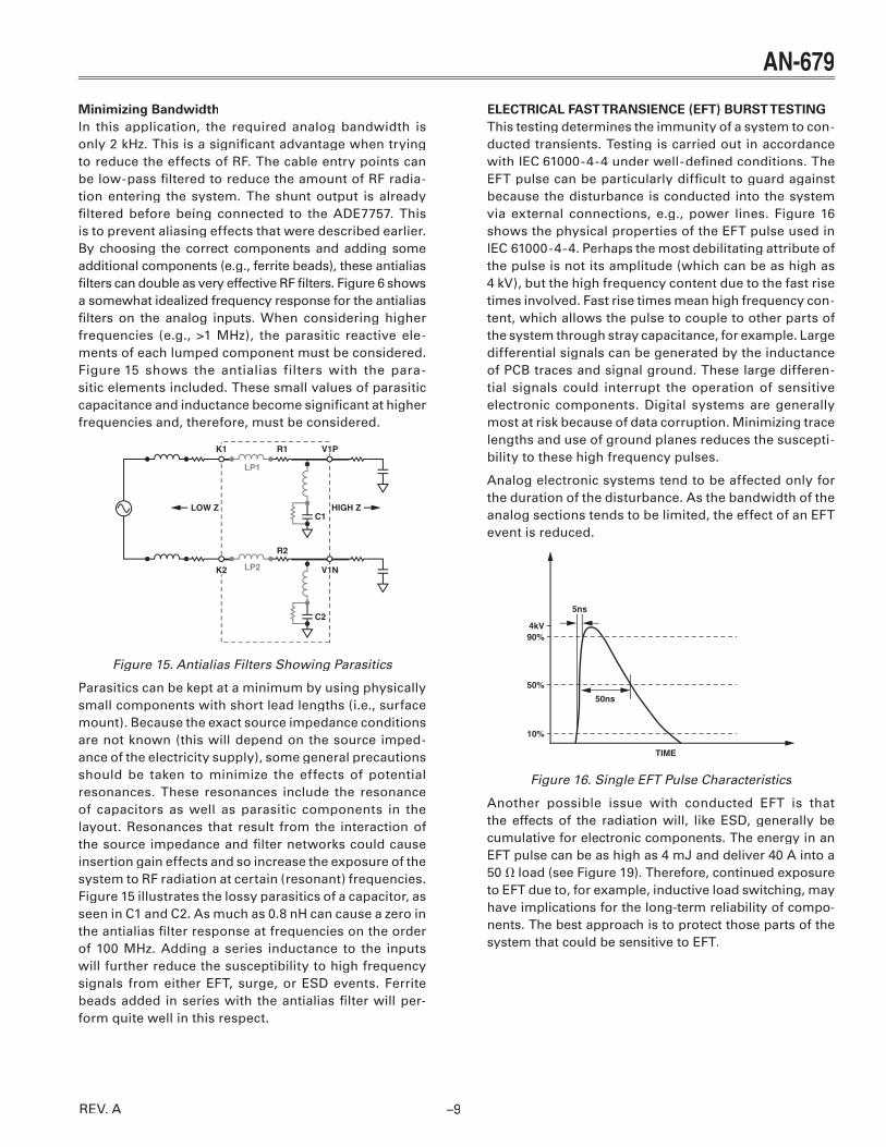
Minimizing BandwidthIn this application, the required analog bandwidth is only 2 kHz. This is a signifi cant advantage when trying to reduce the effects of RF. The cable entry points can be low-pass fi ltered to reduce the amount of RF radia-tion entering the system. The shunt output is already fi ltered before being connected to the ADE7757. This is to prevent aliasing effects that were described earlier. By choosing the correct components and adding some additional components (e.g., ferrite beads), these antialias fi lters can double as very effective RF fi lters. Figure 6 shows a somewhat idealized frequency response for the antialias fi lters on the analog inputs. When considering higher frequencies (e.g., >1 MHz), the parasitic reactive ele-ments of each lumped component must be considered. Figure 15 shows the antialias filters with the para-sitic elements included. These small values of parasitic capacitance and inductance become signifi cant at higher frequencies and, therefore, must be considered.
��
�������������
��
��
��
���
���
���
�� ���
Figure 15. Antialias Filters Showing Parasitics
Parasitics can be kept at a minimum by using physically small components with short lead lengths (i.e., surface mount). Because the exact source impedance conditions are not known (this will depend on the source imped-ance of the electricity supply), some general precautions should be taken to minimize the effects of potential resonances. These resonances include the resonance of capacitors as well as parasitic components in the layout. Resonances that result from the interaction of the source impedance and fi lter networks could cause insertion gain effects and so increase the exposure of the system to RF radiation at certain (resonant) frequencies. Figure 15 illustrates the lossy parasitics of a capacitor, as seen in C1 and C2. As much as 0.8 nH can cause a zero in the antialias fi lter response at frequencies on the order of 100 MHz. Adding a series inductance to the inputs will further reduce the susceptibility to high frequency signals from either EFT, surge, or ESD events. Ferrite beads added in series with the antialias fi lter will per-form quite well in this respect.
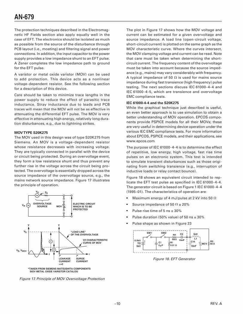
ELECTRICAL FAST TRANSIENCE (EFT) BURST TESTINGThis testing determines the immunity of a system to con-ducted transients. Testing is carried out in accordance with IEC 61000-4-4 under well-defi ned conditions. The EFT pulse can be particularly diffi cult to guard against because the disturbance is conducted into the system via external connections, e.g., power lines. Figure 16 shows the physical properties of the EFT pulse used in IEC 61000-4-4. Perhaps the most debilitating attribute of the pulse is not its amplitude (which can be as high as 4 kV), but the high frequency content due to the fast rise times involved. Fast rise times mean high frequency con-tent, which allows the pulse to couple to other parts of the system through stray capacitance, for example. Large differential signals can be generated by the inductance of PCB traces and signal ground. These large differen-tial signals could interrupt the operation of sensitive electronic components. Digital systems are generally most at risk because of data corruption. Minimizing trace lengths and use of ground planes reduces the suscepti-bility to these high frequency pulses.
Analog electronic systems tend to be affected only for the duration of the disturbance. As the bandwidth of the analog sections tends to be limited, the effect of an EFT event is reduced.
5ns
TIME
4kV90%
50%
10%
50ns
Figure 16. Single EFT Pulse Characteristics
Another possible issue with conducted EFT is that the effects of the radiation will, like ESD, generally be cumulative for electronic components. The energy in an EFT pulse can be as high as 4 mJ and deliver 40 A into a 50 load (see Figure 19). Therefore, continued exposure to EFT due to, for example, inductive load switching, may have implications for the long-term reliability of compo-nents. The best approach is to protect those parts of the system that could be sensitive to EFT.
REV. A
–10–
AN-679
The protection techniques described in the Electromag-netic HF Fields section also apply equally well in the case of EFT. The electronics should be isolated as much as possible from the source of the disturbance through PCB layout (i.e., moating) and fi ltering signal and power connections. In addition, the input capacitor to the power supply provides a low impedance shunt to an EFT pulse. A Zener completes the low impedance path to ground for the EFT pulse.
A varistor or metal oxide varistor (MOV) can be used to add protection. This device acts as a nonlinear voltage-dependent resistor. See the following section for a description of this device.
Care should be taken to minimize trace lengths in the power supply to reduce the effect of parasitic trace inductance. Stray inductance due to leads and PCB traces will mean that the MOV will not be as effective in attenuating the differential EFT pulse. The MOV is very effective in attenuating high energy, relatively long dura-tion disturbances, e.g., due to lightning strikes.
MOV TYPE S20K275The MOV used in this design was of type S20K275 from Siemens. An MOV is a voltage-dependent resistor whose resistance decreases with increasing voltage. They are typically connected in parallel with the device or circuit being protected. During an overvoltage event, they form a low resistance shunt and thus prevent any further rise in the voltage across the circuit being pro-tected. The overvoltage is essentially dropped across the source impedance of the overvoltage source, e.g., the mains network source impedance. Figure 17 illustrates the principle of operation.
����
��
��
� �
��������
����������������� ���
���������������������������������������
�����������������������������
i*������������������
*����������������������������������������������������������������������������
i*������������
it
������������������������������
�
�
Figure 17. Principle of MOV Overvoltage Protection
The plot in Figure 17 shows how the MOV voltage and current can be estimated for a given overvoltage and source impedance. A load line (open-circuit voltage, short-circuit current) is plotted on the same graph as the MOV characteristic curve. Where the curves intersect, the MOV clamping voltage and current can be read. Note that care must be taken when determining the short-circuit current. The frequency content of the overvoltage must be taken into account because the source imped-ance (e.g., mains) may vary considerably with frequency. A typical impedance of 50 is used for mains source impedance during fast transience (high frequency) pulse testing. The next sections discuss IEC 61000-4-4 and IEC 61000-4-5, which are transience and overvoltage EMC compliance tests.
IEC 61000-4-4 and the S20K275While the graphical technique just described is useful, an even better approach is to use simulation to obtain a better understanding of MOV operation. EPCOS compo-nents provide PSPICE models for all their MOVs; these are very useful in determining device operation under the various IEC EMC compliance tests. For more information about EPCOS, PSPICE models, and their applications, see www.epcos.com.
The purpose of IEC 61000-4-4 is to determine the effect of repetitive, low energy, high voltage, fast rise time pulses on an electronic system. This test is intended to simulate transient disturbances such as those origi-nating from switching transience (e.g., interruption of inductive loads or relay contact bounce).
Figure 18 shows an equivalent circuit intended to rep-licate the EFT test pulse as specifi ed in IEC 61000-4-4. The generator circuit is based on Figure 1 IEC 61000-4-4 (1995-01). The characteristics of operation are:
• Maximum energy of 4 mJ/pulse at 2 kV into 50
• Source impedance of 50 ± 20%
• Pulse rise time of 5 ns ± 30%
• Pulse duration (50% value) of 50 ns ± 30%
• Pulse shape as shown in Figure 23
���
��
����
���
����������
�����
�������
���
�������
�������
������
� ��
Figure 18. EFT Generator
REV. A
–11–
AN-679
The simulated output of this generator delivered to a purely resistive 50 load is shown in Figure 19. The open-circuit output pulse amplitude from the generator is 4 kV. Therefore, the source impedance of the generator is 50 , as specifi ed by the IEC 61000-4-4, i.e., ratio of peak pulse output unloaded and loaded (50 ) is 2:1.
���������
�����
����
����
����
����
��
���
���
���
���
���
��
���
���
���
���
������ ���� ���� ���� ���� ����
�������
�����
��������������������������
�������
Figure 19. EFT Generator Output into 50 (No Protection)
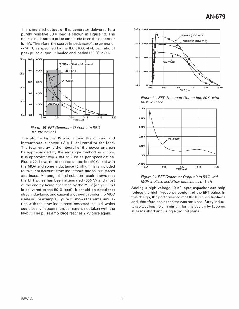
The plot in Figure 19 also shows the current and instantaneous power (V I) delivered to the load. The total energy is the integral of the power and can be approximated by the rectangle method as shown. It is approximately 4 mJ at 2 kV as per specifi cation. Figure 20 shows the generator output into 50 load with the MOV and some inductance (5 nH). This is included to take into account stray inductance due to PCB traces and leads. Although the simulation result shows that the EFT pulse has been attenuated (600 V) and most of the energy being absorbed by the MOV (only 0.8 mJ is delivered to the 50 load), it should be noted that stray inductance and capacitance could render the MOV useless. For example, Figure 21 shows the same simula-tion with the stray inductance increased to 1 H, which could easily happen if proper care is not taken with the layout. The pulse amplitude reaches 2 kV once again.
���������
�����
�����
�����
�����
������ ���� ���� �������� ����
���
���
���
��
��
�������
����������������
������������������
Figure 20. EFT Generator Output into 50 with MOV in Place
TIME (�s)
2.0kV
1.2kV
1.6kV
0.8kV
0.4kV
0V
–0.4kV3.00 3.05 3.10 3.15 3.20
VOLTAGE
Figure 21. EFT Generator Output into 50 with MOV in Place and Stray Inductance of 1 H
Adding a high voltage 10 nF input capacitor can help reduce the high frequency content of the EFT pulse. In this design, the performance met the IEC specifi cations and, therefore, the capacitor was not used. Stray induc-tance was kept to a minimum for this design by keeping all leads short and using a ground plane.
REV. A
–12–
AN-679
IEC 61000-4-5The purpose of IEC 61000-4-5 is to establish a common reference for evaluating the performance of equip-ment when subjected to high energy disturbances on the power and interconnect lines. Figure 22 shows a circuit that was used to generate the combinational wave (hybrid) pulse described in IEC 61000-4-5. It is based on the circuit shown in Figure 1 of IEC 61000-4-5 (2001-04).
Such a generator produces a 1.2 s/50 s open-circuit voltage waveform and an 8 s/20 s short-circuit current waveform, which is why it is referred to as a hybrid generator. The surge generator has an effective output impedance of 2 . This is defi ned as the ratio of peak open-circuit voltage to peak short-circuit current.
���
��
��
����
������
�����
������
�����
�������
���
���
����
������ ��
����������
Figure 22. Surge Generator (IEC 61000-4-5)
Figure 23 shows the generator voltage and current out-put waveforms. The characteristics of the combination wave generator are as follows:
• Open-circuit voltage
– 0.5 kV to at least 4.0 kV
– Waveform as shown in Figure 23
– Tolerance on open-circuit voltage is ±10%
• Short-circuit current
– 0.25 kA to 2.0 kA
– Waveform as shown in Figure 23
– Tolerance on short-circuit current is ±10%
• Repetition rate of at least 60 seconds
���������
�����
�����
�����
�����
��� �� �� ��� ���� � ���
�����
�����
�����
�����
��
Figure 23. Open-Circuit Voltage/Short-Circuit Current
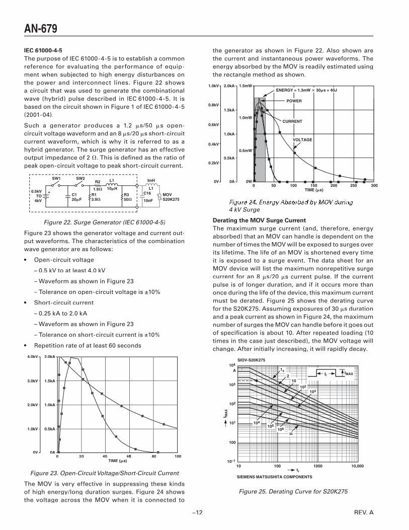
The MOV is very effective in suppressing these kinds of high energy/long duration surges. Figure 24 shows the voltage across the MOV when it is connected to
the generator as shown in Figure 22. Also shown are the current and instantaneous power waveforms. The energy absorbed by the MOV is readily estimated using the rectangle method as shown.
���������
�����
�����
�����
�����
�����
��
�����
�����
�����
��
�����
�����
�����
�����
��� �� ������ ��� ��� ���
�������
�����
�������
���������������������������
Figure 24. Energy Absorbed by MOV during 4 kV Surge
Derating the MOV Surge CurrentThe maximum surge current (and, therefore, energy absorbed) that an MOV can handle is dependent on the number of times the MOV will be exposed to surges over its lifetime. The life of an MOV is shortened every time it is exposed to a surge event. The data sheet for an MOV device will list the maximum nonrepetitive surge current for an 8 s/20 s current pulse. If the current pulse is of longer duration, and if it occurs more than once during the life of the device, this maximum current must be derated. Figure 25 shows the derating curve for the S20K275. Assuming exposures of 30 s duration and a peak current as shown in Figure 24, the maximum number of surges the MOV can handle before it goes out of specifi cation is about 10. After repeated loading (10 times in the case just described), the MOV voltage will change. After initially increasing, it will rapidly decay.
� ��
�
����t�
������������
�����������������������������
�
�� ��� ���� ������
���
���
���
���
���
����
��
��
���
������
���
������
Figure 25. Derating Curve for S20K275
REV. A
–13–
AN-679
EMC Test ResultsThe reference design has been tested for EMC at an independent test house. To ensure the design meets the IEC specifi cations, the meter was subject to limits far above the IEC specifi cations. Testing was carried out by Entela Design & Test Services, Inc., Littleton, MA 01460, USA. The reference design was evaluated for radiated susceptibility (EN 61000-4-3:1998) pursuant to IEC 61036:2000-9 requirements. A copy of the certifi -cation issued for the design is shown in the Test Results section of this application note.
PCB DESIGNBoth susceptibility to conducted or radiated electro-magnetic disturbances and analog performance were considered at the PCB design stage. Fortunately, many of the design techniques used to enhance analog and mixed-signal performance also lend themselves well to improving the EMI robustness of the design. The key idea is to isolate that part of the circuit that is sensi-tive to noise and electromagnetic disturbances. Since the ADE7757 carries out all the data conversion and signal processing, the robustness of the meter will be determined to a large extent by how well protected the ADE7757 is.
Layout for maximizing surge immunity is critical. Distances between traces and various components on the board can affect the overall performance for high voltage immunity. The material used in this application is proprog with a dielectric strength of 1000 V/mil. The spacing between high voltage traces is a minimum of 20 mils for a breakdown of 20 kV through the insulator. Additional precautions include spacing between various components. The air gap between components has a dielectric strength of 75 V/mil, far less than the proprog. For this reason, any exposed leads or components should be spaced 100 mils apart for a breakdown volt-age of 7500 V. Placing components too close together can cause a breakdown between components. During manufacturing, additional steps should be taken to ensure the circuit board is cleaned of impurities. This minimizes any resistive paths that may cause a leakage path during a high voltage event.
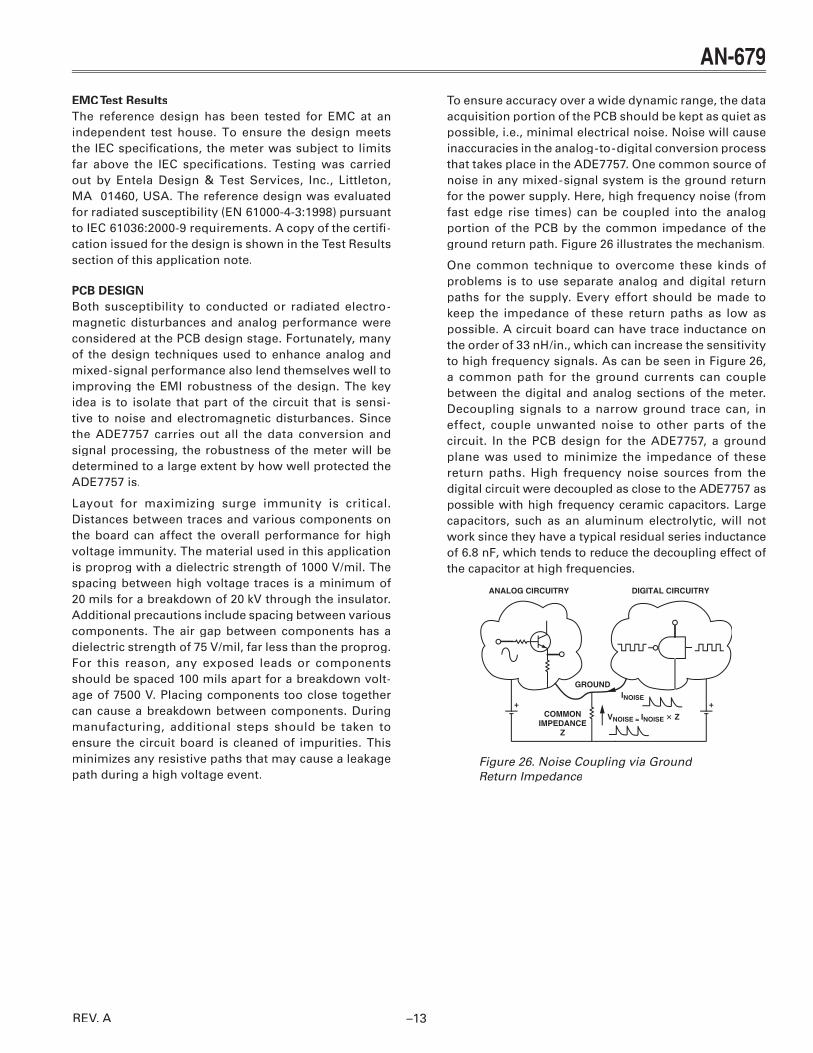
To ensure accuracy over a wide dynamic range, the data acquisition portion of the PCB should be kept as quiet as possible, i.e., minimal electrical noise. Noise will cause inaccuracies in the analog-to-digital conversion process that takes place in the ADE7757. One common source of noise in any mixed-signal system is the ground return for the power supply. Here, high frequency noise (from fast edge rise times) can be coupled into the analog portion of the PCB by the common impedance of the ground return path. Figure 26 illustrates the mechanism.
One common technique to overcome these kinds of problems is to use separate analog and digital return paths for the supply. Every effort should be made to keep the impedance of these return paths as low as possible. A circuit board can have trace inductance on the order of 33 nH/in., which can increase the sensitivity to high frequency signals. As can be seen in Figure 26, a common path for the ground currents can couple between the digital and analog sections of the meter. Decoupling signals to a narrow ground trace can, in effect, couple unwanted noise to other parts of the circuit. In the PCB design for the ADE7757, a ground plane was used to minimize the impedance of these return paths. High frequency noise sources from the digital circuit were decoupled as close to the ADE7757 as possible with high frequency ceramic capacitors. Large capacitors, such as an aluminum electrolytic, will not work since they have a typical residual series inductance of 6.8 nF, which tends to reduce the decoupling effect of the capacitor at high frequencies.
INOISE
GROUND
ANALOG CIRCUITRY DIGITAL CIRCUITRY
COMMONIMPEDANCE
Z
+
VNOISE = INOISE Z
+
Figure 26. Noise Coupling via Ground Return Impedance
REV. A
–14–
AN-679
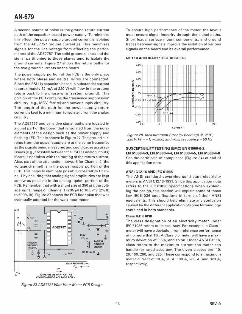
A second source of noise is the ground return current path of the capacitor-based power supply. To minimize this effect, the power supply ground current is isolated from the ADE7757 ground current(s). This minimizes signals for the line voltage from affecting the perfor-mance of the ADE7757. The solid ground planes and the signal partitioning to those planes tend to isolate the ground currents. Figure 27 shows the return paths for the two ground currents on the board.
The power supply portion of the PCB is the only place where both phase and neutral wires are connected. Since the PSU is capacitor-based, a substantial current (approximately 32 mA at 220 V) will fl ow in the ground return back to the phase wire (system ground). This portion of the PCB contains the transience suppression circuitry (e.g., MOV, ferrite) and power supply circuitry. The length of the path for the power supply return current is kept to a minimum to isolate it from the analog circuitry.
The ADE7757 and sensitive signal paths are located in a quiet part of the board that is isolated from the noisy elements of the design such as the power supply and fl ashing LED. This is shown in Figure 27. The ground cur-rents from the power supply are at the same frequency as the signals being measured and could cause accuracy issues (e.g., crosstalk between the PSU as analog inputs) if care is not taken with the routing of the return current. Also, part of the attenuation network for Channel 2 (the voltage channel) is in the power supply portion of the PCB. This helps to eliminate possible crosstalk to Chan-nel 1 by ensuring that analog signal amplitudes are kept as low as possible in the analog (quiet) portion of the PCB. Remember that with a shunt size of 350 , the volt-age signal range on Channel 1 is 35 V to 10.5 mV (2% Ib V to 10.5 mV (2% Ib
to 600% Ib). Figure 27 shows the PCB fl oor plan that was eventually adopted for the watt-hour meter.
ADE7757
DIGITALGROUND(NOISY)
ANALOG GROUND(QUIET)
APPEARS AS PART OF THE COMMON-MODE VOLTAGE FOR V1
32mA FROM PSU
K3
220V
5VK1
K2
70V
IN
OUT
K4
Figure 27. ADE7757 Watt-Hour Meter PCB Design
To ensure high performance of the meter, the layout must ensure signal integrity through the signal paths. Short leads, surface mount components, and ground traces between signals improve the isolation of various signals on the board and its overall performance.
METER ACCURACY/TEST RESULTS
����
����
����
����
��
��
���
���
���
��
���
��
�����
�����
�����
��������� ��� �
��������� ���
�������
�����������
���������
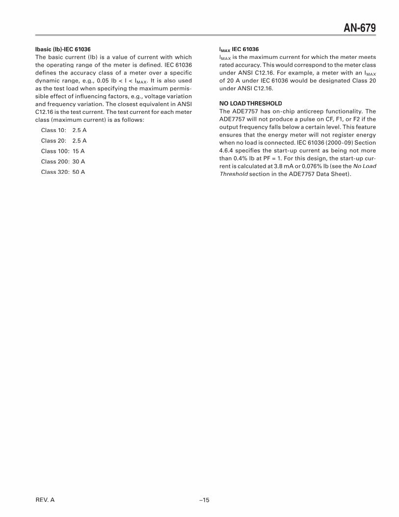
Figure 28. Measurement Error (% Reading) @ 25°C;220 V; PF = +1, +0.866, and –0.5; Frequency = 50 Hz
SUSCEPTIBILITY TESTING (EMC) EN 61000-6-2, EN 61000-4-3, EN 61000-4-4, EN 61000-4-5, EN 61000-4-8See the certifi cate of compliance (Figure 34) at end of this application note.
ANSI C12.16 AND IEC 61036The ANSI standard governing solid-state electricity meters is ANSI C12.16-1991. Since this application note refers to the IEC 61036 specifi cations when explain-ing the design, this section will explain some of those key IEC61036 specifications in terms of their ANSI equivalents. This should help eliminate any confusion caused by the different application of some terminology contained in both standards.
Class IEC 61036The class designation of an electricity meter under IEC 61036 refers to its accuracy. For example, a Class 1 meter will have a deviation from reference performance of no more that 1%. A Class 0.5 meter will have a maxi-mum deviation of 0.5%, and so on. Under ANSI C12.16, class refers to the maximum current the meter can handle for rated accuracy. The given classes are: 10, 20, 100, 200, and 320. These correspond to a maximum meter current of 10 A, 20 A, 100 A, 200 A, and 320 A, respectively.
REV. A
–15–
AN-679
Ibasic (Ib)-IEC 61036The basic current (Ib) is a value of current with which the operating range of the meter is defi ned. IEC 61036 defi nes the accuracy class of a meter over a specifi c dynamic range, e.g., 0.05 Ib < I < IMAX. It is also used as the test load when specifying the maximum permis-sible effect of infl uencing factors, e.g., voltage variation and frequency variation. The closest equivalent in ANSI C12.16 is the test current. The test current for each meter class (maximum current) is as follows:
Class 10: 2.5 A
Class 20: 2.5 A
Class 100: 15 A
Class 200: 30 A
Class 320: 50 A
IMAX IEC 61036IMAX is the maximum current for which the meter meets rated accuracy. This would correspond to the meter class under ANSI C12.16. For example, a meter with an IMAX
of 20 A under IEC 61036 would be designated Class 20 under ANSI C12.16.
NO LOAD THRESHOLDThe ADE7757 has on-chip anticreep functionality. The ADE7757 will not produce a pulse on CF, F1, or F2 if the output frequency falls below a certain level. This feature ensures that the energy meter will not register energy when no load is connected. IEC 61036 (2000-09) Section 4.6.4 specifi es the start-up current as being not more than 0.4% Ib at PF = 1. For this design, the start-up cur-rent is calculated at 3.8 mA or 0.076% Ib (see the No Load Threshold section in the ADE7757 Data Sheet).Threshold section in the ADE7757 Data Sheet).Threshold
REV. A
–16–
AN-679
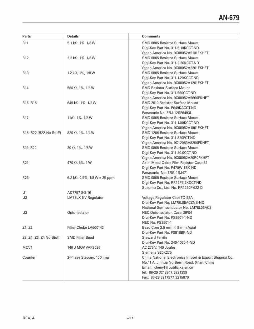
Bill of Materials
Parts Details Comments
C1, C2 Chip Cap 0.022 F ± 10%, 50 V, SMD 0805 Capacitor Surface Mount Multilayer Ceramic, X7R Digi-Key Part No. PCC223BGCT-NDC3 ,C4 Chip Cap 68000 pF ± 10%, 50 V, SMD 0805 Capacitor Surface Mount Multilayer Ceramic, X7R Digi-Key Part No. PCC1838CT-ND Panasonic ECJ-2VB1H333KC5, C7, C12, Chip Cap 0.1 F ± 10%, 16 V, SMD 0805 Capacitor Surface MountC14, C15 Multilayer Ceramic, X7R Digi-Key Part No. BC1300CT-ND BC Components No. 0805B104K160BTC6, C13 Tant Cap 10 F ± 20%, 6.3 V A Case Tant. Surface Mount Digi-Key Part No. PCS1106CT-ND Panasonic No. ECS-TOJY106RC16 (No Stuff) 0.01 F Capacitor, 250 V Class X2 Panasonic ECA-OJFQ221 Digi-Key P5604-NDC17 Cap 0.47 F ± 10%, 630 V Radial Metallized Polyester Digi-Key Part No. EF6474-ND Panasonic No. ECQ-E6474KFC18 Cap 470 F ± 20%, 35 V NHG Radial Electrolytic Digi-Key Part No. P5554-ND Panasonic No. ECA-1VHG471D1, D4 (D4-No Stuff) LED LED Case DIOT1-34 Digi-Key Part No. HLMPD150A-ND Fairchild No. HLMPD150AD2 Rectifying Diode 1 W, 400 V Case DO-41, 1N4004 Digi-Key Part No. 1N4004DICT-ND Diodes, Inc. No. 1N4004-TD3 Zener Diode 1 W, 15 V Case DO-41, 1N4744 A Digi-Key Part No. 1N4744ADICT-ND Diodes, Inc. No. 1N4744-TR1, R2 1.54 k, 1%, 1/8 W SMD 0805 Resistor Surface Mount Digi-Key Part No. 311-1.54KCCT-ND Yageo America No. 9C08052A1541FKHFTR3, R4 499 , 1%, 1/8 W SMD 0805 Resistor Surface Mount Digi-Key Part No. 311-499CCT-ND Yageo America No. 9C08052A4990FKHFTR5 300 k, 1%, 1/2 W SMD 2010 Resistor Surface Mount Digi-Key Part No. P301KACCT-ND Panasonic No. ERJ-12SF3013UR6 150 k, 1%, 1/4 W SMD 1206 Resistor Surface Mount Digi-Key Part No. 311-150KFCT-ND Yageo America No. 9C12063A1503FKHFTR7 75 k, 1%, 1/8 W SMD 0805 Resistor Surface Mount Digi-Key Part No. 311-75.0KCCT-ND Yageo America No. 9C08052A7502FKHFTR8 39 k, 1%, 1/8 W SMD Resistor Surface Mount Digi-Key Part No. 311-39.0KCCT-ND Yageo America No. 9C08052A3902FKHFTR9 18 k, 1%, 1/8 W SMD 0805 Resistor Surface Mount Digi-Key Part No. 311-18.0KCCT-ND Yageo America No. 9C08052A1802FKHFTR10 9.1 k, 1%, 1/8 W SMD 0805 Resistor Surface Mount Digi-Key Part No. 311-9.10KCCT-ND Yageo America No. 9C08052A9101FKHFT
REV. A
–17–
AN-679
Parts Details Comments
R11 5.1 k, 1%, 1/8 W SMD 0805 Resistor Surface Mount Digi-Key Part No. 311-5.10KCCT-ND Yageo America No. 9C08052A5101FKHFTR12 2.2 k, 1%, 1/8 W SMD 0805 Resistor Surface Mount Digi-Key Part No. 311-2.20KCCT-ND Yageo America No. 9C08052A2201FKHFTR13 1.2 k, 1%, 1/8 W SMD 0805 Resistor Surface Mount Digi-Key Part No. 311-1.20KCCT-ND Yageo America No. 9C08052A1201FKHFTR14 560 , 1%, 1/8 W SMD Resistor Surface Mount Digi-Key Part No. 311-560CCT-ND Yageo America No. 9C08052A5600FKHFTR15, R16 649 k, 1%, 1/2 W SMD 2010 Resistor Surface Mount Digi-Key Part No. P649KACCT-ND Panasonic No. ERJ-12SF6493UR17 1 k, 1%, 1/8 W SMD 0805 Resistor Surface Mount Digi-Key Part No. 311-1.00KCCT-ND Yageo America No. 9C08052A1001FKHFTR18, R22 (R22-No Stuff) 820 , 1%, 1/4 W SMD 1206 Resistor Surface Mount Digi-Key Part No. 311-820FCT-ND Yageo America No. 9C12063A8200FKHFTR19, R20 20 , 1%, 1/8 W SMD 0805 Resistor Surface Mount Digi-Key Part No. 311-20.0CCT-ND Yageo America No. 9C08052A20R0FKHFTR21 470 , 5%, 1 W Axial Metal Oxide Film Resistor Case 32 Digi-Key Part No. P470W-1BK-ND Panasonic No. ERG-1SJ471 R23 6.2 k, 0.5%, 1/8 W ± 25 ppm SMD 0805 Resistor Surface Mount Digi-Key Part No. RR12P6.2KDCT-ND Susumu Co., Ltd. No. RR1220P-622-DU1 AD7757 SO-16U2 LM78LX 5 V Regulator Voltage Regulator Case TO-92A Digi-Key Part No. LM78L05ACZNS-ND National Semiconductor No. LM78L05ACZU3 Opto-isolator NEC Opto-isolator, Case DIP04 Digi-Key Part No. PS2501-1-ND NEC No. PS2501-1Z1, Z2 Filter Choke LA600140 Bead Core 3.5 mm 9 mm Axial Digi-Key Part No. P9818BK-NDZ3, Z4 (Z3, Z4 No-Stuff) SMD Filter Bead Steward Ferrite Digi-Key Part No. 240-1030-1-NDMOV1 140 J MOV VAR9026 AC 275 V, 140 Joules Siemens S20K275Counter 2-Phase Stepper, 100 imp China National Electronics Import & Export Shaanxi Co. No.11 A, Jinhua Northern Road, Xi’an, China Email: [email protected] Tel: 86-29 3218247, 3221399 Fax: 86-29 3217977, 3215870
REV. A
–18–
AN-679
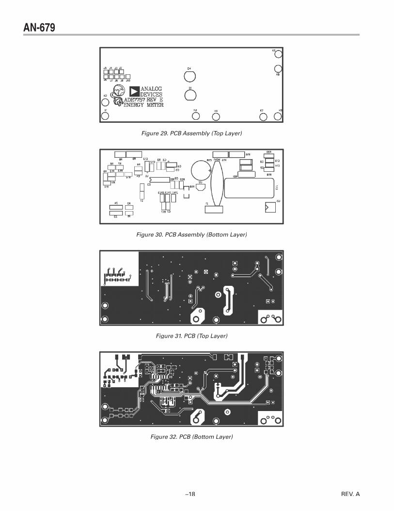
Figure 29. PCB Assembly (Top Layer)
Figure 30. PCB Assembly (Bottom Layer)
Figure 31. PCB (Top Layer)
Figure 32. PCB (Bottom Layer)
REV. A
–19–
AN-679
1
2
3
4
5
6
7
8
16
15
14
13
12
11
10
9
VDD
REF
J11
J13
J13
J12
J11
J12
VDD
V2P
V2N
V1N
V1P
AGND
REFIN/OUT
SCF
F1
F2
CF
DGND
REVP
RCLKIN
S0
S1ADE7757
U1
REF
AGND
AGND
+ C610�F
C50.1�F
PS2501
U3
C140.1�F
C150.1�F
R1920�
R2020�
R18820�
R236.2k�
R22820�
R171k�
C70.1�F
R6150k�
R5300k�
R775k�
R839k�
R918k�
R109.1k�
R115.1k�
R122.2k�
R131.2k�
R14560�
J20�
J30�
J40�
J50�
J60�
J70�
J80�
J90�
J100�
CALHIGH
CALLOW
VDD
AGND
+ C1310�F
C120.1�F
C20.022�F
C10.022�F
C30.068�F
C40.068�F
1
2
3VIN VOUT
GND
VDD
CALHIGH
AGNDAGND
AGND
AGND
AGND
AGND
AGND
AGND
AGND
R4499�
R3499�
K2
K1
K3
K4
Z3VAL
Z2VAL
Z1VAL
Z4VAL
R11.54k�
R15649k�
R16649k�
R21470�
C170.47�F
C160.01�F
R21.54k�
K
A
A K
D4HLMPD150
HLMPD150
VDD
JP11
JP12
JP13
D1
K8
K5
K6
K7
+C18470�F
D3IN4744
D2IN4004
MOV1140J
U2LM78L05
CALLOW
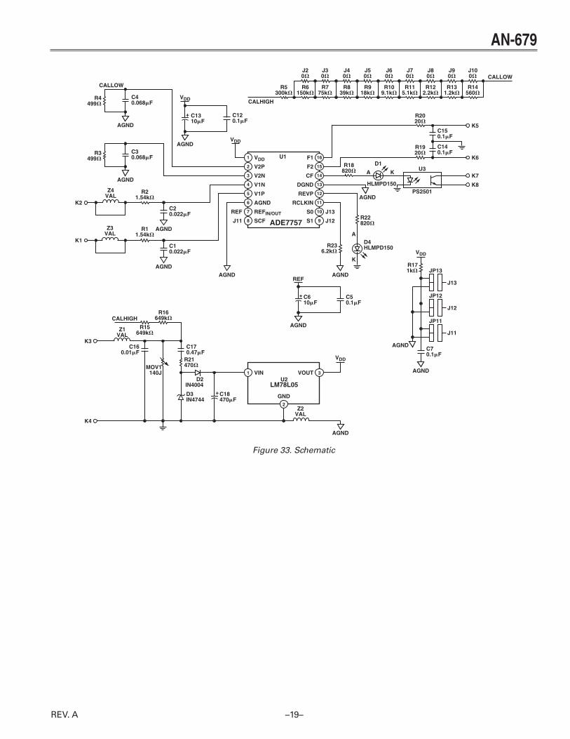
Figure 33. Schematic
REV. A

E04
471–
0–4/
04(A
)
–20–© 2004 Analog Devices, Inc. All rights reserved. Trademarks and registered trademarks are the property of their respective owners.
AN-679
Figure 34. Certifi cate of Compliance
REV. A