AN 238: Using Quartus II Verilog HDL & VHDL Integrated...
53
Altera Corporation 1 December 2002, ver. 1.2 Application Note 238 AN-238-1.2 Introduction The Altera ® Quartus ® II software includes improved integrated synthesis that fully supports the Verilog HDL and VHDL languages and provides options to control the synthesis process. With this synthesis support, the Quartus II software provides a complete, easy-to-use, standalone solution for system-on-a-programmable-chip (SOPC) designs. In addition to describing Quartus II synthesis support, this application note explains how you can improve Quartus II synthesis results by: ■ Using Quartus II synthesis options ■ Using design planning practices ■ Using synchronous design methodologies ■ Following Altera-recommended guidelines for writing HDL code ■ Following guidelines for using architectural features of Altera devices (instantiating and inferring Altera megafunctions) 1 The dialog boxes and settings described in this document reflect the Quartus II software version 2.2. If you are using another version of Quartus II software, the settings may be different. Refer to Quartus II Help for your version for information on the appropriate dialog boxes and settings. Verilog HDL & VHDL Support The Quartus II software’s integrated synthesis fully supports Verilog HDL and VHDL synthesizable language features, as well as some compiler directives. f For information on specific syntax features and language constructs, refer to the “Quartus II Verilog HDL Support” and “Quartus II VHDL Support” topics in Quartus II Help. Verilog HDL The Quartus II Compiler’s Logic Synthesizer module supports the Verilog-2001 standard (IEEE Std. 1364-1995) and some Verilog-2001 standard (IEEE Std. 1364-2001) constructs. You can select which standard to use in the in the Settings dialog box (Assignments menu). Select Verilog HDL Input under HDL Input Settings in the Category list. The Compiler uses Verilog-2001 by default. Using Quartus II Verilog HDL & VHDL Integrated Synthesis
Transcript of AN 238: Using Quartus II Verilog HDL & VHDL Integrated...

December 2002, ver. 1.2 Application Note 238
Using Quartus IIVerilog HDL & VHDLIntegrated Synthesis
Introduction The Altera® Quartus® II software includes improved integrated synthesis that fully supports the Verilog HDL and VHDL languages and provides options to control the synthesis process. With this synthesis support, the Quartus II software provides a complete, easy-to-use, standalone solution for system-on-a-programmable-chip (SOPC) designs.
In addition to describing Quartus II synthesis support, this application note explains how you can improve Quartus II synthesis results by:
■ Using Quartus II synthesis options■ Using design planning practices■ Using synchronous design methodologies■ Following Altera-recommended guidelines for writing HDL code■ Following guidelines for using architectural features of Altera
devices (instantiating and inferring Altera megafunctions)
1 The dialog boxes and settings described in this document reflect the Quartus II software version 2.2. If you are using another version of Quartus II software, the settings may be different. Refer to Quartus II Help for your version for information on the appropriate dialog boxes and settings.
Verilog HDL & VHDL Support
The Quartus II software’s integrated synthesis fully supports Verilog HDL and VHDL synthesizable language features, as well as some compiler directives.
f For information on specific syntax features and language constructs, refer to the “Quartus II Verilog HDL Support” and “Quartus II VHDL Support” topics in Quartus II Help.
Verilog HDL
The Quartus II Compiler’s Logic Synthesizer module supports the Verilog-2001 standard (IEEE Std. 1364-1995) and some Verilog-2001 standard (IEEE Std. 1364-2001) constructs. You can select which standard to use in the in the Settings dialog box (Assignments menu). Select Verilog HDL Input under HDL Input Settings in the Category list. The Compiler uses Verilog-2001 by default.
Altera Corporation 1
AN-238-1.2
AN 238: Using Quartus II Verilog HDL & VHDL Integrated Synthesis
1 The code samples provided in this document follow the Verilog-2001 standard.
Verilog-2001 support is a new feature in the Quartus II software version 2.1 and later. Supported constructs include:’
■ Generate statements: generate and genvar■ localparam constants■ Preprocessor statements such as ‘elsif, ‘line, ‘ifdef, and ‘file■ Signed declarations for all variables■ Operators such as **, <<<, and >>> ■ Attributes using the syntax (* name = value *)■ Indexed part selects using +: and -:■ Combinational logic sensitivity wild card token @*
f Refer to Quartus II Help for a complete listing of supported constructs.
The Quartus II software supports case-sensitive Verilog HDL code, per the Verilog HDL standard. Before version 2.1, the Quartus II software did not support case-sensitive module names.
VHDL
The Quartus II Compiler’s Logic Synthesizer module supports the VHDL 1987 (IEEE Std. 1076-1987) and 1993 (IEEE Std. 1076-1993) standards. You can select which standard to use in the in the Settings dialog box (Assignments menu). Select VHDL Input under HDL Input Settings in the Category list. The Compiler uses VHDL 1993 by default.
1 The code samples provided in this document follow the VHDL 1993 standard.
The Quartus II software now supports VHDL libraries differently from older versions of the Quartus II or MAX+PLUS® II software. In version 2.1 and later, standard IEEE and vendor VHDL libraries and packages can be called from VHDL code within the Quartus II software.
The IEEE library includes the standard VHDL packages std_logic_1164, numeric_std, and numeric_bit. The STD library is part of the VHDL language standard and includes packages standard (included in every project by default) and textio. For compatibility with older designs, the Quartus II software also supports vendor-specific packages/libraries, including:
■ Synopsys packages such as std_logic_arith and std_logic_unsigned in the IEEE library
2 Altera Corporation

AN 238: Using Quartus II Verilog HDL & VHDL Integrated Synthesis
■ Mentor Graphics packages such as std_logic_arith in the ARITHMETIC library
■ Altera packages such as maxplus2, altera_mf_components, and lpm_components in the ALTERA library
f For a complete listing of library and package support, refer to the “Using Quartus II Packages” topic in Quartus II Help.
The Quartus II software does not support user-defined precompiled libraries because standard third-party synthesis tools do not support these precompiled libraries and these libraries do not provide significant reduction in compilation times. In older Quartus II versions, you declared precompiled libraries in the VHDL Input tab of the General Settings dialog box (Project menu).
To call a user-defined VHDL package in Quartus II version 2.1 and later, indicate the library and package name using the LIBRARY and USE commands. You can use any name for your library, including work; therefore, you can use current software versions for projects developed with older versions of Altera software that used precompiled libraries without the need to modify any code. To compile these projects, include the VHDL package in your Quartus II project by going to the Add/Remove page under Files & Directories in the Settings dialog box (Assignments menu). The package must be listed before other files that use the package because it must be analyzed by the Quartus II Compiler first.
Synthesis Options
The Quartus II software provides a number of options to guide the synthesis process and achieve optimal results. You can use compiler directives, attributes, and Quartus II logic options to control synthesis.
1 Versions of Quartus II software earlier than 2.1 did not support compiler directives or attributes; the software treated these options as comments. Quartus II behavior is different if designs compiled in earlier versions of the software included these synthesis options. You may need to change your code now that the software recognizes these options.
This section defines three types of synthesis options, compiler directives, attributes, and Quartus II logic options. It also describes each of the following options:
■ Translate Off & On■ Read Comments as HDL■ Full Case■ Parallel Case■ Preserve Registers
Altera Corporation 3

AN 238: Using Quartus II Verilog HDL & VHDL Integrated Synthesis
■ Maximum Fan-Out■ Optimization Technique■ State Machine Processing■ Preserve Hierarchical Boundary■ Power-Up High■ Power-Up Don’t Care■ Remove Duplicate Logic■ Remove Duplicate Registers■ Remove Redundant Logic Cells
Compiler Directives
The Quartus II software supports compiler directives, also called pragmas. You include compiler directives in Verilog HDL or VHDL code as comments. These directives are not Verilog HDL or VHDL commands; however, synthesis tools use them to drive the synthesis process in a particular manner. Other tools such as simulators ignore these directives and treat them as comments.
You can enter compiler directives in your code using the following syntax, where directive and value are variables and the entry within brackets is optional.
Verilog HDL:
// synthesis <directive> { <value> }or/* synthesis <directive> { <value> } */
VHDL:
-- synthesis <directive> { <value> }
1 In addition to the synthesis keyword shown above, the keywords pragma, synopsys, and exemplar are supported in both Verilog HDL and VHDL for compatibility with other synthesis tools.
Attributes
The Quartus II software supports attributes, also known as pragmas or directives. Attributes are similar to compiler directives in that they drive the synthesis process; however, attributes always apply to a specific design element. Some attributes are also available as Quartus II logic options.
4 Altera Corporation

AN 238: Using Quartus II Verilog HDL & VHDL Integrated Synthesis
The Verilog-2001 and VHDL language definitions provide specific syntax for specifying attributes. However in Verilog-1995 HDL you must use comments similar to compiler directives. You can enter attributes in your code using the following syntax, where attribute, attribute type, value, object, and object type are variables and the entry within brackets is optional.
Verilog-1995 HDL:
// synthesis <attribute> { <value> } or/* synthesis <attribute> { <value> } */
1 You cannot use the open one-line comment in Verilog HDL when a semicolon is required at the end of the line because it is not clear to which HDL element the attribute applies.
In addition to the synthesis keyword as shown above, the keywords, pragma, synopsys, and exemplar are supported for compatibility with other synthesis tools.
Verilog-2001 HDL:
(* <attribute> { = <value> } *)
VHDL:
attribute <attribute> : <attribute type> ;attribute <attribute> of <object> : <object type> is <value> ;
In this application note, the examples demonstrate each syntax form.
Quartus II Logic Options
Quartus II logic options control many aspects of the place-and-route process, including synthesis. You can set logic options in the Quartus II user interface through the Assignment Organizer (Assignments menu) or Assignment Editor (Assignments menu). Quartus II logic options allow you to set the associated attributes without editing the source HDL code.
Quartus II Synthesis Options
Table 1 lists the Quartus II synthesis options that this application note discusses. Some options are simply compiler directives, some are only available as either attributes or logic options, and some are available as both attributes and logic options.
Altera Corporation 5

AN 238: Using Quartus II Verilog HDL & VHDL Integrated Synthesis
1 Because Verilog HDL is case-sensitive, compiler directives and attributes are also case sensitive.
The following sections provide more information on each option shown in Table 1.
Translate Off & On
The translate_off and translate_on compiler directives indicate whether the Quartus II software or a third-party synthesis tool should compile a portion of HDL code that is not relevant for synthesis. The translate_off directive marks the beginning of code that the synthesis tool should ignore; the translate_on directive indicates that synthesis should resume. A common use of these directives is to indicate a portion of code that is intended for simulation only. The synthesis tool reads synthesis-specific directives and processes them during synthesis; however, third-party simulation tools read the directives as comments and ignore them. Figures 1 and 2 show examples of these directives.
Table 1. Synthesis Options as Compiler Directives, Attributes & Logic Options
Synthesis Option Compiler Directive Attribute Quartus II Logic Option
Translate Off and On translate_off
translate_on
– –
Read Comments as HDL read_comments_as_HDL – –
Full Case – full_case –
Parallel Case – parallel_case –
Preserve Registers – preserve
syn_preserve
Preserve Registers
Maximum Fan-Out – maxfan
syn_maxfan
Maximum Fan-Out
Optimization Technique – – Optimization Technique
State Machine Processing – – State Machine Processing
Preserve Hierarchical Boundary
– – Preserve Hierarchical Boundary
Power-Up High – – Power-Up High
Power-Up Don’t Care – – Power-Up Don’t Care
Remove Duplicate Logic – – Remove Duplicate Logic
Remove Duplicate Registers
– – Remove Duplicate Registers
Remove Redundant Logic Cells
– – Remove Redundant Logic Cells
6 Altera Corporation

AN 238: Using Quartus II Verilog HDL & VHDL Integrated Synthesis
Figure 1. Verilog HDL Example of Translate On & Off
// synthesis translate_off parameter tpd = 2; // Delay for simulation
#tpd;// synthesis translate_on
Figure 2. VHDL Example of Translate On & Off
-- synthesis translate_off use std.textio.all; -- synthesis translate_on
Read Comments as HDL
The read_comments_as_HDL compiler directive indicates that the Quartus II software should compile a portion of HDL code that is commented out. This directive allows you to comment out portions of HDL source code that are not relevant for simulation, while instructing the Quartus II software to read and synthesize that same source code. Setting the read_comments_as_HDL directive to on marks the beginning of commented code that the synthesis tool should read; setting the read_comments_as_HDL directive to off indicates the end of the code.
1 You can use the directive with translate_off and translate_on to create one HDL source file that includes both a megafunction instantiation for synthesis and a behavioral description for simulation.
In Figures 3 and 4, the commented code enclosed by read_comments_as_HDL is visible to the Quartus II Compiler and is synthesized.
1 Compiler directives are case-sensitive in Verilog HDL; you must match the case of the directive as shown in Figure 3
Figure 3. Verilog HDL Example of Read Comments as HDL
// synthesis read_comments_as_HDL on// my_rom lpm_rom (.address (address),// .data (data));// synthesis read_comments_as_HDL off
Altera Corporation 7

AN 238: Using Quartus II Verilog HDL & VHDL Integrated Synthesis
Figure 4. VHDL Example of Read Comments as HDL
-- synthesis read_comments_as_HDL on-- my_rom : entity lpm_rom-- port map (-- address => address,-- data => data, );-- synthesis read_comments_as_HDL off
Full Case
The full_case attribute indicates that a Verilog HDL case statement should be considered full, that is, either all possible binary combinations of cases are specified or a default case is present. A full case attribute attached to a case statement header that is not full forces the unspecified states to be treated as logic “don’t care” values. Using this attribute on a case statement that is not full avoids latch inference as discussed in “Latches” on page 22. VHDL case statements must be full, so the attribute does not apply.
The case statement in Figure 5 is not full because not all binary values for sel are specified. Because the full_case attribute is used, synthesis treats the output as “don’t care” when the sel input is 2’b11.
Figure 5. Sample Verilog HDL Code with a full_case Attribute
module full_case (a, sel, y);input [3:0] a;input [1:0] sel;output y;reg y;
always @(a or sel)case (sel) // synthesis full_case
2’b00: y=a[0];2’b01: y=a[1];2’b10: y=a[2];
endcaseendmodule
Verilog-2001 syntax also accepts the following statements in the case header instead of the comment form as shown in Figure 5:
(* full_case *) case (sel)
8 Altera Corporation

AN 238: Using Quartus II Verilog HDL & VHDL Integrated Synthesis
When using the full_case attribute, there is a potential cause for simulation-mismatch between Verilog HDL functional and post-Quartus II simulation because unknown case statement cases may still function like latches during functional simulation. For example, this mismatch occurs if a full_case attribute is specified and it does change synthesis. In this example, when sel is 2’b11 a functional HDL simulation output behaves like a latch while the Quartus II simulation output behaves like “don’t care.”
Parallel Case
The parallel_case attribute indicates that a Verilog HDL case statement should be considered parallel, that is, only one case item can be matched at a time. A parallel case attribute attached to a case statement header forces the synthesis tool to generate multiplexer logic instead of a priority encoder. VHDL case statements have no overlap in any of the case items, so they are always parallel and this attribute does not apply.
Use this attribute only when the case statement is truly parallel and you want to use one-hot style encoding. If you use the attribute in any other situation, the generated logic will not match the functional HDL simulation.
The example in Figure 6 shows a casez statement with non-parallel cases. Functional HDL simulation behaves as a priority encoder with bits of sel having high to low priority order sel[2], sel[1], and sel[0]. However, the synthesized version of this design may simulate differently because it will be implemented with multiplexer logic.
Figure 6. Sample Verilog HDL Code with a parallel_case Attribute
module parallel_case (sel, a, b, c);input [2:0] sel;output a, b, c;reg a, b, c;
always @(sel)begin
{a, b, c} = 3’b0;casez (sel) // synthesis parallel_case
3’b1??: a = 1’b1;3’b?1?: b = 1’b1;3’b??1: c = 1’b1;
endcaseend
endmodule
Altera Corporation 9

AN 238: Using Quartus II Verilog HDL & VHDL Integrated Synthesis
Verilog-2001 syntax also accepts the following statements in the case header instead of the comment form as shown in Figure 6:
(* parallel_case *) casez (sel)
Preserve Registers
This attribute and logic option directs the compiler not to minimize or remove a specified register during synthesis optimization or sequential netlist optimization. Sequential optimizations can eliminate redundant registers and registers with constant drivers. This option can preserve a register so you can observe it during simulation or with the SignalTap® II logic analyzer. Additionally, it can preserve registers if you are creating a preliminary version of the design in which secondary signals are not specified. The option cannot preserve registers that have no fan-out.
You can set the Preserve Registers logic option in the Quartus II user interface or you can set the preserve attribute in your HDL code as shown below. In this example, the my_reg register is preserved.
1 In addition to preserve, the Quartus II software supports the syn_preserve attribute name for compatibility with other synthesis tools.
Verilog HDL:
reg my_reg /* synthesis preserve */;
Verilog-2001:
(* preserve *) reg my_reg;
VHDL:
signal my_reg : stdlogic;
attribute preserve : boolean;attribute preserve of my_reg : signal is true;
1 Setting the Preserve Registers logic option in the Quartus II software version 2.2 does not affect registers that are removed during the analysis and elaboration stage of compilation (before logic synthesis). To fully preserve the register throughout compilation, use the HDL attribute instead of the logic option.
10 Altera Corporation

AN 238: Using Quartus II Verilog HDL & VHDL Integrated Synthesis
Maximum Fan-Out
This attribute and logic option directs the compiler to control the number of destinations fed by a node. The fan-out count of the node will not exceed the value specified for the maximum number of fan-out. You can apply this option to a register, pin, or a logic cell buffer. This option is useful for reducing the load of critical signals, which can improve performance. Additionally, you can use this option to instruct the compiler to duplicate or replicate a register that feeds nodes in different locations on the target device. Duplicating the register may allow the Fitter to place these new registers closer to their destination logic, minimizing routing delay.
This option is available for all devices supported in the Quartus II software except for MAX®, FLEX®, ACEX®, and Mercury™ devices.
You can set the Maximum Fanout logic option in the Quartus II user interface, or you can set the maxfan attribute in your HDL code as shown below. In this example, the compiler duplicates the clk_gen register so its fan-out is not greater than 50.
1 In addition to maxfan, the Quartus II software supports the syn_maxfan attribute name for compatibility with other synthesis tools.
Verilog HDL:
reg clk_gen /* synthesis maxfan 50 */;
Verilog-2001:
(* maxfan = 50 *) reg clk_gen;
VHDL:
signal clk_gen : stdlogic;
attribute maxfan : integer ;attribute maxfan of clk_gen : integer is 50;
Altera Corporation 11

AN 238: Using Quartus II Verilog HDL & VHDL Integrated Synthesis
Optimization Technique
This logic option specifies the overall goal for logic optimization, i.e., whether to attempt to achieve maximum speed performance or minimum area usage during compilation. Table 2 lists the settings for this option, which you can only apply to a design entity.
The default setting varies by target device family, and is generally optimized to get the best area/speed trade-off. Results are design and device-dependent and can vary depending on which design or device family you use.
State Machine Processing
This logic option specifies the processing style used to compile a state machine. Table 3 lists the settings for this option, which you can apply to a state machine name or to a design entity containing a state machine.
1 The Compiler in the Quartus II software versions 2.1 and 2.2 does not report Verilog HDL state machines. The software correctly reads and implements state machine logic during synthesis, however, the Compiler does not report state information and you cannot change the encoding using Quartus II logic options.
Table 2. Optimization Technique Settings
Setting Description
Area The Compiler makes the design as small as possible to minimize resource usage.
Speed The Compiler chooses a design implementation that has the fastest fMAX.
Table 3. State Machine Processing Settings
Setting Description
Auto (Default) Allows the Compiler to choose the best encoding for the state machine.
Minimal Bits Uses the least number of bits to encode the state machine.
One-Hot Encodes the state machine in the one-hot style.
User-Encoded Encodes the state machine in the manner specified by the user.
12 Altera Corporation

AN 238: Using Quartus II Verilog HDL & VHDL Integrated Synthesis
Preserve Hierarchical Boundary
This logic option determines how strictly the hierarchical boundaries between design entities should be maintained during logic synthesis. Table 4 lists the settings for the option, which you can only apply to a design entity. Lower-level entities do not inherit their parent entity’s setting for this option.
The Relaxed setting means that the Compiler preserves hierarchical boundaries; however, certain signals such as VCC and GND are propagated and optimized through the boundaries. The Firm setting does not allow optimization across boundaries, and keeps each hierarchical block separate.
Power-Up High
This logic option causes a register (flipflop) to power up with a high logic level (1). Turning this option off for a register causes the register to power up with a low logic level (0). You can apply this option to any register or to a pin with the logic configurations described as follows:
■ If this option is turned on for an input pin, the option is transferred automatically to the register that is driven by the pin if the following conditions are present:
– There is no intervening logic, other than inversion, between the pin and the register.
– The input pin drives the data input of the register.– The input pin does not fan out to any other logic.
Table 4. Preserve Hierarchical Boundary Settings
Setting Description
Off Completely ignores boundaries and therefore allows unlimited optimization. This setting provides the greatest logic minimization.
Relaxed Allows only partial cross-boundary optimization, which may reduce the compilation time. Non-trivial inputs and outputs of the entity are visible during simulation and timing analysis.
Firm Strictly maintains hierarchical boundaries. This setting may increase compilation time, increase logic cell count, and negatively affect design performance.
Altera Corporation 13

AN 238: Using Quartus II Verilog HDL & VHDL Integrated Synthesis
■ If this option is turned on for an output or bidirectional pin, it is transferred automatically to the register that feeds the pin if the following conditions are present:
– There is no intervening logic, other than inversion, between the register and the pin.
– The register does not fan out to any other logic.
Power-Up Don’t Care
This logic option causes registers to power up with a “don’t care” logic level (X), or the logic level most appropriate for the design. You might use this option to allow the Compiler to change the power-up level of a register to minimize your design’s area usage.
For example, a register may have its D input tied to VCC. If you turned this option off, the register powers up low even though it goes high at the first clock signal. If you turned this option on, the Compiler sets the power-up value of the register to high and, therefore, can eliminate the register and connect the output of the register to VCC. If the Compiler makes this type of optimization, it issues you a message indicating it is doing so.
This project-wide option does not apply to registers that have the Power-Up High logic option set (either on or off).
1 Versions of the Quartus II software earlier than version 2.1 did not include this option. If you compile an older design that relies on registers to power-up to a specific level, the Compiler may synthesize the design differently. Turn off the Power-Up Don’t Care option if you want your design to use the power-up behavior of older versions of Quartus II software.
Remove Duplicate Logic
If you turn on this option, the Compiler removes logic if it is identical to other logic in the design. If two functions generate the same logic, the Compiler removes the second one and the first one fans out to the second one’s destinations. Additionally, if the deleted logic function has different logic option assignments, the Compiler ignores them. This option is turned on by default.
When turned on, this option also removes all duplicate registers, like the Remove Duplicate Registers option. If you do not want the Compiler to remove certain registers when this option is turned on, turn off the Remove Duplicate Registers option for those registers. See Table 5 for additional details.
14 Altera Corporation

AN 238: Using Quartus II Verilog HDL & VHDL Integrated Synthesis
If you turn this option off, the Compiler does not remove duplicate logic that you inserted deliberately. If a function’s output feeds an LCELL buffer, the Compiler always treats it as a unique signal and the Remove Duplicate Logic option does not apply (i.e., the Compiler does not remove an LCELL buffer if you turn on this option).
Remove Duplicate Registers
If you turn on this logic option, it removes a register if it is identical to another register. If two registers generate the same logic, the Compiler removes the second one and the first one fans out to the second one’s destinations. Also, if the deleted register has different logic option assignments, the Compiler ignores them. This option is turned on by default.
The Compiler only recognizes this option if you turned on the Remove Duplicate Logic option. When turned on, the Remove Duplicate Logic option also removes duplicate registers. Therefore, you should use the Remove Duplicate Registers option only if you want to prevent the Compiler from removing duplicate registers that you have used deliberately. That is, you should use this option only with the Off setting. See Table 5. You can apply this option to an individual register or a design entity that contains registers.
Remove Redundant Logic Cells
This logic option removes redundant LCELL primitives or WYSIWYG cells. If you turn this option On, the Compiler optimizes a circuit for area and speed. The project-wide option is turned Off by default.
Table 5. Settings for Remove Duplicate Logic and Remove Duplicate Registers
Remove Duplicate Logic Setting
Remove Duplicate Registers Setting
Description
On (Default) On (Default) Removes logic (including registers) if it is identical to other logic in the design.
On Off Preserves all registers for which the Remove Duplicate Registers option is turned off. Removes logic (including any other registers) if it is identical to other logic in the design.
Off On or Off Preserves duplicate logic and registers.
Altera Corporation 15

AN 238: Using Quartus II Verilog HDL & VHDL Integrated Synthesis
Design Planning
Before you begin a new Verilog HDL or VHDL design, you must first determine your design methodology. For example, you should decide whether you will use a top-down or hierarchical bottom-up methodology, and whether you want to use a block-based design flow. For hierarchical design flows, you should partition your design for the best performance and easiest optimization. This section describes design planning considerations, including:
■ Top-Down vs. Bottom-Up Design Methodology■ Block-Based Design with the Quartus II LogicLock™ Methodology■ Hierarchical Design Partitioning
Top-Down vs. Bottom-up Design Methodology
Most HDL-based designs use either a top-down or bottom-up (block-based) design methodology. In top-down designs, you apply a single optimization to the design’s top level. Thus, a top-down synthesis flow has one output netlist file for the entire design.
As designs become more complex and designers work in teams, a block-based design flow is often more effective. In this approach, you perform optimization on individual sub-blocks and each sub-block has its own output netlist file. After you optimize all of the sub-blocks, you integrate them into a final design and optimize it at the top level. Synthesizing and optimizing each sub-block separately may provide better overall quality of results.
Table 6 describes some of the advantages of each synthesis flow.
Table 6. Top-Down vs. Bottom-up Design Flow
Design Flow Description Advantages
Top-down One output netlist for the entire design.
You can perform optimization across design boundaries and hierarchies for the entire design.
Simple to manage.
Bottom-up (block-based)
Separate netlist files for each design module.
You compile each module separately.
You can apply different optimization techniques to each module.
Design modifications do not affect the optimization of other modules.
You can use optimized modules in other designs.
16 Altera Corporation

AN 238: Using Quartus II Verilog HDL & VHDL Integrated Synthesis
Block-Based Design with the Quartus II LogicLock Methodology
You can use the LogicLock design methodology in the Quartus II software to perform block-based (bottom-up) compilation. Using the LogicLock design flow, you can design and optimize each module independently, integrate all optimized modules into a top-level design, and then verify the overall system. Incorporating each module into the top-level design does not affect the performance of each module.
f For more information on using the LogicLock feature in the Quartus II software and the LogicLock design flow, see AN 161: Using the LogicLock Methodology in the Quartus II Design Software.
To take advantage of the LogicLock design methodology when synthesizing a design in the Quartus II software, you must create an atom netlist for each design module before you lock down any nodes into LogicLock regions. The atom netlist contains design information that fully describes the module’s logic in terms of the device architecture. In the atom netlist, the nodes are fixed as Altera primitives and the node names do not change if the atom netlist does not change. If a node name does change, any placement information made to that node (such as LogicLock assignments made when back-annotating a region) is invalid and is ignored by the Compiler.
If you synthesize the design using a third-party tool and then compile in the Quartus II software, an atom netlist already exists and the node names are fixed. If you synthesize the design as a VHDL Design File (.vhd), Verilog Design File (.v), Text Design File (.tdf), or a Block Design File (.bdf) in the Quartus II software, you must also create an atom netlist to fix the nodes and node names. During compilation, the Quartus II software can create a Verilog Quartus Mapping File (.vqm) in the atom_netlists subdirectory in the project directory.
f For instructions on creating an atom netlist in the Quartus II software, refer to the “Saving Synthesis Results for an Entity to a Verilog Quartus Mapping File” topic in Quartus II Help.
Hierarchical Design Partitioning
In a hierarchical design flow, you use the Quartus II software to create multiple design files and then link them together in a hierarchy. With this structure, you can simulate and optimize the individual modules that comprise the design separately. You can also use the LogicLock design methodology to follow a block-based bottom-up design methodology. When following a hierarchical design methodology, it is important to consider how the design is partitioned.
Altera Corporation 17

AN 238: Using Quartus II Verilog HDL & VHDL Integrated Synthesis
Altera recommendations for partitioning designs are as follows:
■ Partition the design at functional boundaries.
■ Minimize the I/O connections between different partitions.
■ Do not use “glue logic” between hierarchical blocks. If you preserve hierarchy boundaries, glue logic is not merged with hierarchical blocks. The Quartus II software may optimize glue logic separately, which can degrade synthesis results and is not efficient when used with the LogicLock design methodology.
■ Limit clocks to one per block. Partitioning the design in clock domains makes synthesis and timing analysis easier.
■ Place state machines in separate blocks to speed optimization and provide greater encoding control.
■ Separate timing-critical functions from non-timing-critical functions.
■ Limit the critical timing path to one hierarchical block. You can group the logic from several design blocks to ensure the critical path resides in one block.
■ Register all inputs and/or outputs of each block, which makes logic synchronous and avoids glitches. Also, registering outputs may eliminate the need to specify required output times for different blocks.
18 Altera Corporation

AN 238: Using Quartus II Verilog HDL & VHDL Integrated Synthesis
Synchronous Design
The most important design practice for FPGA designers to follow is synchronous design. The basic principle of synchronous design is that a clock signal triggers all events. As long as all of the registers’ timing requirements are met, a synchronous design behaves in a predictable and reliable manner for all process, voltage, and temperature (PVT) conditions. Typically, designers can easily target synchronous designs to different device families or speed grades. Additionally, if you want to target your design to a HardCopy™ device, synchronous design practices can ensure a successful migration.
Fundamentals of Synchronous Design
In a synchronous design, everything is related to the clock signal as described below:
■ On every active edge of the clock (usually the rising edge), the data inputs of registers are sampled and transferred to outputs.
■ Following an active clock edge, the outputs of registers are memorized and isolated from the data inputs.
■ Following an active clock edge, combinational logic (feeding the data inputs of registers) changes values. This change triggers a period of instability due to propagation delays through the logic. The signals go through a number of transitions, and finally settle to new values.
■ Changes happening on data inputs of registers do not affect the values of their outputs until the next active clock edge.
Because the internal circuitry of registers isolates data inputs from outputs, instability in the combinational logic does not affect the intended operation of the design as long as the following timing requirements are met:
■ Before an active clock edge, the data input is settled for at least the setup time of the register.
■ After an active clock edge, the data input remains stable for at least the hold time of the register.
Altera Corporation 19
AN 238: Using Quartus II Verilog HDL & VHDL Integrated Synthesis
When the setup time or hold time of a register is violated, the output can be set to an intermediate voltage level between the high and low levels, which is called a metastable state. Such a state is not fully stable and small perturbations, like noise in power rails, can return the register to a valid state. Various undesirable effects can occur, e.g., the propagation delay can increase, and the output can move to the wrong state. In some cases, the output can even oscillate between the two valid states for a relatively long time.
Hazards in Asynchronous Design
Designs that do not follow synchronous design practices are said to be asynchronous. In the past, designers often used asynchronous techniques such as ripple counters or pulse generators in FPGA designs. Historically, such techniques enabled designers to take “short cuts” and save device resources. Because Altera devices now provide large amounts of high-performance logic gates, registers, and memory, resource and performance trade-offs have changed. With programmable logic designs approaching the complexity and performance levels of ASICs, you should focus on design practices that help you meet your design goals consistently. Asynchronous design techniques have inherent problems, such as relying on propagation delays within a device. These techniques lead to incomplete timing constraints and generate possible glitches and spikes.
Some asynchronous design structures rely on the relative propagation delays of signals to function correctly. Design structures in Altera devices can have different timing delays, depending on how the design is placed and routed in the device. Therefore, you cannot determine the timing delay associated with a particular block of logic ahead of time. Additionally, as devices become faster because of process improvements, the delays in an asynchronous design may decrease, resulting in a design that does not function as expected. Relying on a particular delay makes asynchronous designs very difficult to migrate to different devices or speed grades, including HardCopy devices.
The timing of asynchronous design structures is often difficult or impossible to model with timing assignments and constraints. If you do not have complete or accurate timing constraints, the Quartus II software timing-driven algorithms may not be able to perform the best optimizations, and reported results will not be complete.
20 Altera Corporation

AN 238: Using Quartus II Verilog HDL & VHDL Integrated Synthesis
Some asynchronous design structures can generate harmful glitches and spikes, pulses that are very short compared to clock periods. Glitches affect a signal that transitions from zero-to-one or one-to-zero. Instead of a single transition, the signal exhibits a number of transitions before stabilizing to its final value. Spikes affect a signal that should remain steady. Instead of keeping its current value, the signal exhibits a number of transitions before returning to its value.
Most glitches and spikes are generated by combinational logic. When the inputs of combinational logic change, the outputs exhibit a number of glitches and spikes before they settle to their new values. Therefore, incorrect values can be propagated through the combinational logic, leading to incorrect values on the outputs in asynchronous designs. In a synchronous design, glitches and spikes on the data inputs of registers are normal events that have no negative consequences because the data is not processed until the clock edge.
General Coding Style Guidelines
When designing with HDL code, it is important to understand how a synthesis tool interprets different HDL coding styles and the results to expect. Your coding style can affect logic utilization and timing performance. This section discusses some basic coding style guidelines to ensure optimal synthesis results for Altera designs.
Combinational Loops
Combinational loops are one of the most common causes of instability and unreliability in digital designs. In a synchronous design, all feedback loops should include registers. Combinational loops violate synchronous design principles by establishing a direct feedback with no registers. For example, a combinational loop occurs when the left-hand side of an arithmetic expression also appears on the right-hand side. Additionally, a combinational loop occurs when you feed back the output of a register to an asynchronous control pin of the same register through combinational logic, as shown in Figure 7.
Figure 7. Combinational Loop through a Register’s Asynchronous Clear Pin
LogicCloud
CLRN
D Q
Altera Corporation 21

AN 238: Using Quartus II Verilog HDL & VHDL Integrated Synthesis
Combinational loops are inherently high-risk design structures because of the following reasons:
■ The behavior of a combinational loop generally depends on the relative propagation delays through the logic involved in the loop. As discussed in “Hazards in Asynchronous Design” on page 20, propagation delays can change and the behavior of the loop may change.
■ Some design tools have problems handling combinational loops that cause endless computation loops. When encountering a combinational loop, most tools break it open so that they can proceed. All the tools used in the design flow may open a given loop a different manner, processing it in a way that may not be consistent with the original design intent.
Latches
In digital logic, latches hold the value of a signal until a new value is assigned. Latches can also be inferred from HDL code to hold a value when the designer did not intend to use a latch. Altera devices are register-intensive; therefore, designing with latches uses more logic and leads to lower performance than designing with registers.
Latches can also cause various difficulties in the design. Although latches are memory elements like registers, they are fundamentally different. When a latch is in a feed-through mode, there is a direct path between the data input and the output. Glitches and spikes on the data input can pass to the output, and you should take care to avoid possible timing hazards. The timing for latches is also inherently ambiguous. When analyzing a design with a D latch, for example, the software cannot determine whether you intended to transfer data to the output on the leading edge of the clock or on the trailing edge. As a result, timing analysis of latches is difficult. In many cases, only the original designer knows the full intent of the design; therefore, another designer cannot easily migrate the design to other devices or reuse the code.
When designing combinational logic, certain coding styles can create an unintentional latch. For example, when CASE or IF statements do not cover all possible conditions of the inputs, combinational feedback can generate latches to hold the output if a new output value is not assigned. The full_case attribute can be used in Verilog HDL designs to indicate that non-specified cases can be treated as “don’t care.” However, using the full_case attribute may lead to simulation mismatches because it is a synthesis-only attribute. Refer to “Full Case” on page 8 for details.
22 Altera Corporation
AN 238: Using Quartus II Verilog HDL & VHDL Integrated Synthesis
Omitting the final ELSE clause or WHEN OTHERS clause in an IF or CASE statement can also generate a latch. “Don’t care” assignments on the default conditions tend to prevent latch generation. Synthesis software generally treats unknowns as “don’t care” conditions to optimize logic. Within a design, assign the default CASE or final ELSE value to “don’t care” instead of to a logic value for the best logic optimization.
Figure 8 shows sample VHDL code that prevents an unintentional latch. Without the final ELSE clause, the code creates unintentional latches to cover the remaining combinations of the sel inputs. When targeting the code in Figure 8 for a Stratix™ device, omitting the final ELSE condition causes the Compiler to use 6 logic elements (LEs) instead of the 3 LEs it uses with the ELSE statement. Assigning the final value to 1 instead of X results in 4 LEs.
Figure 8. Sample VHDL Code Preventing Unintentional Latch Creation’LIBRARY ieee;USE IEEE.std_logic_1164.all;
ENTITY nolatch ISPORT (a,b,c : IN STD_LOGIC;
sel: IN STD_LOGIC_VECTOR (4 DOWNTO 0);oput: OUT STD_LOGIC);
END nolatch;
ARCHITECTURE rtl OF nolatch ISBEGIN
PROCESS (a,b,c,sel) BEGINIF sel = "00000" THEN
oput <= a;ELSIF sel = "00001" THEN
oput <= b;ELSIF sel = "00010" THEN
oput <= c;ELSE --- Prevents latch inference
oput <= 'X'; --/END IF;
END PROCESS;END rtl;
Internally Generated & Gated Clocks
Avoid using internally generated and gated clocks where possible because they can cause both functional and timing problems in the design. Internally generated clocks can introduce glitches and spikes that create functional problems. If you use the outputs of combinational logic as clock signals (or asynchronous reset signals), you should expect glitches and spikes.
Altera Corporation 23
AN 238: Using Quartus II Verilog HDL & VHDL Integrated Synthesis
In a synchronous design, glitches and spikes on data inputs of registers are normal events that have no consequences. However, a glitch or a spike on the clock input (or an asynchronous input of a register) can have significant consequences such as the following:
■ Glitches and spikes are narrow pulses that can violate the minimum pulse width requirements of the register.
■ If the data input of the register is changing when a glitch or spike reaches the clock input, the design may violate setup and hold times.
■ Even if the design does not violate timing requirements, the register output can change value unexpectedly and cause functional hazards elsewhere in the design.
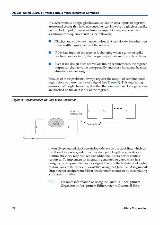
Because of these problems, always register the output of combinational logic before you use it as a clock signal (see Figure 9). This registering ensures that the glitches and spikes that the combinational logic generates are blocked on the data input of the register.
Figure 9. Recommended On-Chip Clock Generation
Internally generated clocks create logic delays on the clock line, which can result in clock skew greater than the data path length in your design. Routing the clock may also require additional Altera device routing resources. To implement an internally generated or gated clock in a design, you can promote the clock signal to one of the high-fan-out global routing lines in the device (if available) using the Quartus II Assignment Organizer or Assignment Editor (Assignment menu), or by instantiating a GLOBAL primitive.
1 For more information on using the Quartus II Assignment Organizer or Assignment Editor, refer to Quartus II Help.
LogicCloud
Clock
On-Chip Clock
No Risk of Glitch or Spike
24 Altera Corporation
AN 238: Using Quartus II Verilog HDL & VHDL Integrated Synthesis
Divided Clocks & Ripple Counters
Many designs need clocks created by dividing a master clock. Always use synchronous counters or state machines to divide a master clock. Additionally, create your design such that flipflops always directly generate divided clock signals. Your design should never decode the outputs of a counter or a state machine to generate clock signals; this implementation causes glitches and spikes.
1 Many Altera devices include PLL circuitry that can perform clock division, see the device family data sheet for details.
FPGA designers have often implemented ripple counters to divide clocks by a power of two because the counters use fewer gates than their synchronous counterparts. Ripple counters use cascaded registers, in which the output pin of each register feeds the clock pin of the register in the next stage. This cascading can cause problems because the counter creates a ripple clock at each stage. These ripple clocks have to be handled as such in timing analysis, which can be difficult and may require you to at least enter appropriate timing assignments in the Quartus II software.
Synchronous Clock Enables vs. Gated Clocks
Gated clocks can be a powerful technique to reduce power consumption. When a clock is gated, both the clock tree and flipflops no longer toggle, eliminating their contributions to switching power. Gated clocks turn a clock signal on and off using an enable signal that controls some sort of gating circuitry. When a clock is turned off, the corresponding clock domain is shut down and becomes functionally inactive.
Gated clocks are not part of a synchronous scheme. Therefore, they can significantly increase the design implementation and verification effort, posing challenges in some cases.
From a functional point of view, you can shut down a clock domain in a purely synchronous manner using a synchronous clock enable. However, when using a synchronous clock enable scheme, the clock tree keeps toggling and the internal circuitry of flipflops remains active (although outputs do not change values), which does not reduce power consumption. Therefore, you should use a synchronous scheme unless you want to turn off clocks for power reduction.
Altera Corporation 25

AN 238: Using Quartus II Verilog HDL & VHDL Integrated Synthesis
Using Synchronous Clock Enables
To turn off a clock domain in a synchronous manner, insert a multiplexer in front of the data input of every register to either load new data or copy the output of the register (see Figure 10). Altera FPGAs efficiently support synchronous clock enables.
Figure 10. Synchronous Clock Enable Block Diagram
Using Gated Clocks
You should use gated clocks only when your target application requires substantial power reduction. If you must use gated clocks, implement them according to the robust clock-gating technique shown in Figure 11. If you do not adhere to this scheme, you may have difficulty verifying your design or migrating the design to another device. In worst-case scenarios, gated clocks can cause design failures because of glitches and spikes.
You can gate a clock signal at the root of the clock tree, at the leaves, or somewhere in between. Because the clock tree contributes to switching power, always generate the clock at the root so that you can shut down the entire clock tree instead of gating it further along the clock tree at the leaves.
0
1
Enable Clock
LogicCloud
26 Altera Corporation

AN 238: Using Quartus II Verilog HDL & VHDL Integrated Synthesis
Figure 11. Recommended Clock Gating Technique Block Diagram
As shown in Figure 11, a register generates the enable command to ensure that it is free of glitches and spikes. The design clocks the register that generates the enable command on the inactive edge of the clock to be gated (use the falling edge when gating a clock that is active on the rising edge as in Figure 11). With this implementation, only one input of the gate that turns the clock on and off changes at a time, which does not generate glitches or spikes on the output. Use an AND gate to gate a clock that is active on the rising edge. For a clock that is active on the falling edge, use an OR gate to gate the clock and register the enable command with a positive-edged register.
When using this scheme, you should pay attention to the duty cycle of the clock because only the on-time can generate the enable command. This situation might cause problems if the logic that generates the enable command is particularly complex, or if the duty cycle of the clock is severely unbalanced. However, the duty cycle is a minor issue compared to the problems created by other methods of gating clocks.
Multiplexed Clocks
Clock multiplexing is used to operate the same logic function with different clock sources. Multiplexing logic of some kind selects a clock source, as shown in Figure 12. For example, telecommunications applications that deal with multiple frequency standards often use multiplexed clocks.
Clock
GatedClock
Gating Circuit
Enable
Clock
Enable
Gated Clock
LogicCloud
Altera Corporation 27

AN 238: Using Quartus II Verilog HDL & VHDL Integrated Synthesis
Figure 12. Multiplexing Logic & Clock Sources
Requirements for multiplexed clocks can vary widely depending on the application. Clock multiplexing is acceptable if the following conditions are met:
■ The clock multiplexing logic does not change after initial configuration.
■ The design uses multiplexing logic to select a clock for testing purposes.
■ You always apply a reset when switching clocks. ■ A temporarily incorrect response of the chip following clock
switching has no consequences.
If the design switches clocks on the fly with no reset and your design cannot tolerate a temporarily incorrect response of the chip, then you must use a synchronous design so that there are no timing violations on the registers, no glitches or spikes on clock signals, no race conditions, etc.
State Machines
The Quartus II software can encode state machines during synthesis. To improve performance when coding state machines, Altera recommends that you observe the following guidelines:
■ Represent the states in a state machine by defined labels/enumerated types. This implementation makes the state machine easier to read and reduces the risk of errors during coding.
■ Assign default values to outputs derived from the state machine to avoid generation of unwanted latches during synthesis.
■ Assign a default clause to direct the state machine in case it accidentally reaches an unused state.
Clock 1
MultiplexedClock
LogicCloud
Clock 2
Select
28 Altera Corporation

AN 238: Using Quartus II Verilog HDL & VHDL Integrated Synthesis
■ For Verilog HDL, use the parallel_case attribute with case statements for one-hot functionality. Use if and else_if statements for all intentional priority encoders.
■ Separate the state machine logic from all arithmetic functions and data paths, including assigning output values.
1 The Compiler in the Quartus II software versions 2.1 and 2.2 does not report Verilog HDL state machines. The software correctly reads and implements state machine logic during synthesis, however, the Compiler does not report state information and you cannot change the encoding using Quartus II logic options.
Architecture-Specific Coding Style Guidelines
This section discusses coding style guidelines to ensure optimal synthesis results when using architectural features of Altera devices. The section also provides code examples for inferring Altera megafunctions from HDL code in the Quartus II software.
Altera Megafunctions
Altera provides parameterizable megafunctions that are optimized for Altera device architectures. Megafunctions include the library of parameterized modules (LPM), device-specific embedded megafunctions such as phase-locked loops (PLLs), Stratix DSP blocks, LVDS drivers, intellectual property (IP) available as Altera MegaCore® functions, and IP available from Altera Megafunction Partners Program (AMPPSM) partners.
Using megafunctions instead of coding your own logic can save valuable design time. Additionally, these functions can offer more efficient logic synthesis and device implementation. It is easy to scale megafunctions to different sizes by simply setting parameters.
You must use megafunctions to access some Altera device-specific features, such as memory, DSP blocks, LVDS drivers, PLLs, and DDIO circuitry. You can use megafunctions by instantiating them in your HDL code or inferring them from generic HDL code.
Instantiating Altera Megafunctions in HDL Code
You can instantiate Altera megafunctions in your HDL design by:
■ Using the MegaWizard® Plug-In Manager to parameterize the function and create a wrapper file.
■ Instantiating the function using the port and parameter definition.
Altera Corporation 29

AN 238: Using Quartus II Verilog HDL & VHDL Integrated Synthesis
Using the MegaWizard Plug-In Manager
Altera recommends that you use the Quartus II MegaWizard Plug-In Manager to instantiate megafunctions. The wizard provides a graphical interface for customizing and parameterizing megafunctions, and ensures that you set all megafunction parameters properly. When you finish setting parameters, the wizard generates a VHDL or Verilog HDL wrapper file that instantiates the megafunction with the correct parameters (it also creates a Component Declaration file for VHDL). You can then instantiate the wrapper file in your HDL code.
1 Altera strongly recommends that you use the wizard for complex megafunctions such as PLLs and LVDS drivers.
Table 7 lists the files the MegaWizard Plug-In Manager generates and describes each file.
Notes to Table 7:(1) The wizard only generates this file if you select AHDL output files.(2) The wizard only generates this file if you select VHDL output files.(3) The wizard only generates this file if you select Verilog HDL output files.
f For more information about how to use the MegaWizard Plug-In Manager, refer to Quartus II Help.
Table 7. MegaWizard Plug-In Manager Generated Files
File Description
<output file>.bsf Symbol for the megafunction used in the Quartus II schematic editor.
<output file>.cmp Component Declaration File.
<output file>.inc Include File for the module in the megafunction wrapper file.
<output file>.tdf (1) Megafunction wrapper file for instantiation in an AHDL design.
<output file>.vhd (2) Megafunction wrapper file for instantiation in a VHDL design.
<output file>.v (3) Megafunction wrapper file for instantiation in a Verilog HDL design.
<output file>_bb.v (3) Hollow-body declaration of the module in the megafunction wrapper file used in Verilog HDL designs to specify port directions when using third-party synthesis tools.
<output file>_inst.tdf (1) Sample AHDL instantiation of the subdesign in the megafunction wrapper file.
<output file>_inst.vhd (2) Sample VHDL instantiation of the entity in the megafunction wrapper file.
<output file>_inst.v (3) Sample Verilog HDL instantiation of the module in the megafunction wrapper file.
30 Altera Corporation

AN 238: Using Quartus II Verilog HDL & VHDL Integrated Synthesis
Using the Port & Parameter Definition
You can instantiate the megafunction directly in your Verilog HDL or VHDL code by calling the function like any other module or component. In VHDL, you also need to use a Component Declaration. Refer to Quartus II Help (or your IP documentation) for a list of the megafunctions’s ports and parameters. Help also provides a sample VHDL Component Declaration.
Inferring Megafunctions from HDL Code
The Quartus II Logic Synthesizer automatically recognizes certain types of HDL code and infers the appropriate megafunction. That is, the software uses the Altera megafunction code when compiling your design even though you did not specifically instantiate the megafunction. The software uses inference because the megafunctions are optimized for Altera devices, so the area and/or performance may be better than generic HDL code. Additionally, you must use megafunctions to access certain architecture-specific features—such as RAM, DSP blocks, and shift registers—that generally provide improved performance compared to basic logic elements.
The following sections describe the types of logic that the Quartus II Logic Synthesizer recognizes and maps to megafunctions. The software only infers these specific functions that are described by HDL code. The software cannot infer other megafunctions, such as PLLs and LVDS drivers, from HDL code because these functions cannot be fully or efficiently described in HDL. In some cases, the Quartus II software has an option that you can use to disable inference.
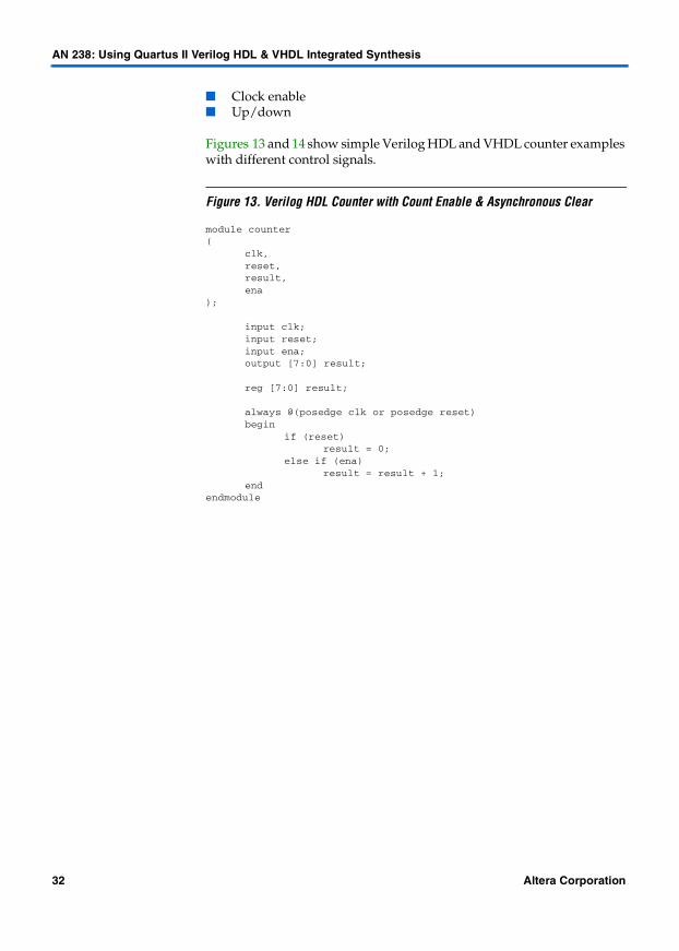
Counters
The Quartus II Logic Synthesizer looks for any set of registers that feeds itself through a plus-one adder, a minus-one adder, or both, and converts the registers and logic to an lpm_counter megafunction. If the design also has logic implementing counter signals, the software can recognize them as well. Specifically, the Quartus II software recognizes the following signals:
■ Asynchronous clear■ Asynchronous set (only to all ones)■ Asynchronous load■ Count enable■ Synchronous clear■ Synchronous set (only to all ones)■ Synchronous load
Altera Corporation 31
AN 238: Using Quartus II Verilog HDL & VHDL Integrated Synthesis
■ Clock enable■ Up/down
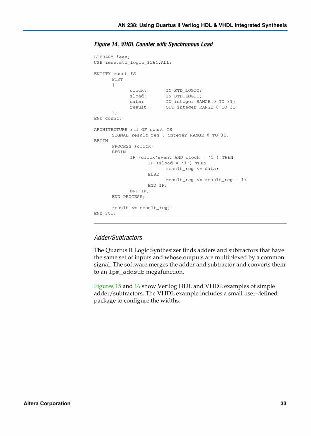
Figures 13 and 14 show simple Verilog HDL and VHDL counter examples with different control signals.
Figure 13. Verilog HDL Counter with Count Enable & Asynchronous Clear
module counter(
clk,reset,result,ena
);
input clk;input reset;input ena;output [7:0] result;
reg [7:0] result;
always @(posedge clk or posedge reset)begin
if (reset) result = 0;
else if (ena) result = result + 1;
endendmodule
32 Altera Corporation
AN 238: Using Quartus II Verilog HDL & VHDL Integrated Synthesis
Figure 14. VHDL Counter with Synchronous Load’LIBRARY ieee;USE ieee.std_logic_1164.ALL;
ENTITY count ISPORT(
clock: IN STD_LOGIC;sload: IN STD_LOGIC;data: IN integer RANGE 0 TO 31;result: OUT integer RANGE 0 TO 31
);END count;
ARCHITECTURE rtl OF count ISSIGNAL result_reg : integer RANGE 0 TO 31;
BEGINPROCESS (clock)BEGIN
IF (clock'event AND clock = '1') THENIF (sload = '1') THEN
result_reg <= data;ELSE
result_reg <= result_reg + 1;END IF;
END IF;END PROCESS;
result <= result_reg;END rtl;
Adder/Subtractors
The Quartus II Logic Synthesizer finds adders and subtractors that have the same set of inputs and whose outputs are multiplexed by a common signal. The software merges the adder and subtractor and converts them to an lpm_addsub megafunction.
Figures 15 and 16 show Verilog HDL and VHDL examples of simple adder/subtractors. The VHDL example includes a small user-defined package to configure the widths.
Altera Corporation 33

AN 238: Using Quartus II Verilog HDL & VHDL Integrated Synthesis
Figure 15. Verilog HDL Adder/Subtractor
module addsub (a, b, addnsub, result);
input [7:0] a;input [7:0] b;input addnsub;output [8:0] result;
always @(a or b or addnsub)begin
if (addnsub)result = a + b;
elseresult = a - b;
endendmodule
Figure 16. VHDL Adder/Subtractor’LIBRARY ieee;USE ieee.std_logic_1164.ALL;
PACKAGE my_package ISCONSTANT ADDER_WIDTH : integer := 5;CONSTANT RESULT_WIDTH : integer := 6;
SUBTYPE ADDER_VALUE IS integer RANGE 0 TO 2 ** ADDER_WIDTH - 1;SUBTYPE RESULT_VALUE IS integer RANGE 0 TO 2 ** RESULT_WIDTH - 1;
END my_package;
LIBRARY ieee;USE ieee.std_logic_1164.ALL;USE work.my_package.ALL;
ENTITY addsub ISPORT(
a: IN ADDER_VALUE;b: IN ADDER_VALUE;addnsub: IN STD_LOGIC;result: OUT RESULT_VALUE
);END addsub;
ARCHITECTURE rtl OF addsub ISBEGIN
PROCESS (a, b, addnsub)BEGIN
IF (addnsub = '1') THENresult <= a + b;
ELSEresult <= a - b;
END IF;END PROCESS;
END rtl;
34 Altera Corporation

AN 238: Using Quartus II Verilog HDL & VHDL Integrated Synthesis
Multipliers
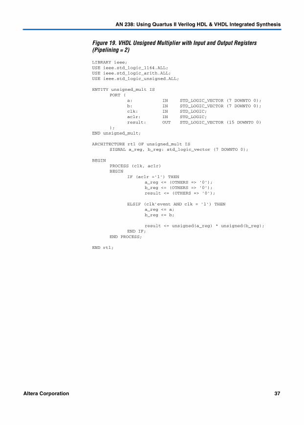
The Quartus II Logic Synthesizer finds multipliers and converts them to lpm_mult megafunctions. For devices with DSP blocks, the software may implement the lpm_mult function in a DSP block instead of LEs, depending on device utilization. The Quartus II Fitter may also place input and output registers in DSP blocks (i.e., perform register packing) to improve performance and LE utilization.
f For more information on the DSP block and which functions it can implement, refer to the appropriate Altera device family data sheet and the DSP Solutions Center on the Altera web site at http://www.altera.com.
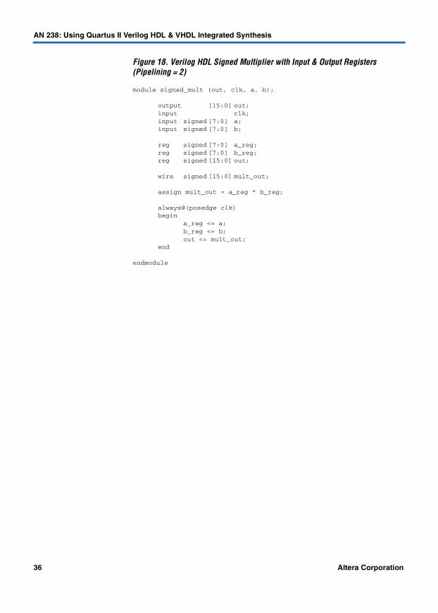
Figures 17 through 20 show Verilog HDL and VHDL examples for unsigned and signed multipliers that the Quartus II Compiler infers as an lpm_mult. Each example fits into one DSP block 9-bit element (using no LEs for registers when register packing occurs).
1 The signed declaration in Verilog HDL is a feature of the Verilog-2001 standard.
Figure 17. Verilog HDL Unsigned Multiplier
module unsigned_mult (out, a, b);
output [15:0] out;input [7:0] a;input [7:0] b;
assign out = a * b;
endmodule
Altera Corporation 35
AN 238: Using Quartus II Verilog HDL & VHDL Integrated Synthesis
Figure 18. Verilog HDL Signed Multiplier with Input & Output Registers (Pipelining = 2)
module signed_mult (out, clk, a, b);
output [15:0] out;input clk;input signed [7:0] a;input signed [7:0] b;
reg signed [7:0] a_reg;reg signed [7:0] b_reg;reg signed [15:0] out;
wire signed [15:0] mult_out;
assign mult_out = a_reg * b_reg;
always@(posedge clk)begin
a_reg <= a;b_reg <= b;out <= mult_out;
end
endmodule
36 Altera Corporation
AN 238: Using Quartus II Verilog HDL & VHDL Integrated Synthesis
Figure 19. VHDL Unsigned Multiplier with Input and Output Registers (Pipelining = 2)’LIBRARY ieee;USE ieee.std_logic_1164.ALL;USE ieee.std_logic_arith.ALL;USE ieee.std_logic_unsigned.ALL;
ENTITY unsigned_mult ISPORT (
a: IN STD_LOGIC_VECTOR (7 DOWNTO 0);b: IN STD_LOGIC_VECTOR (7 DOWNTO 0);clk: IN STD_LOGIC;aclr: IN STD_LOGIC;result: OUT STD_LOGIC_VECTOR (15 DOWNTO 0)
);END unsigned_mult;
ARCHITECTURE rtl OF unsigned_mult ISSIGNAL a_reg, b_reg: std_logic_vector (7 DOWNTO 0);
BEGIN
PROCESS (clk, aclr)BEGIN
IF (aclr ='1') THENa_reg <= (OTHERS => '0');b_reg <= (OTHERS => '0');result <= (OTHERS => '0');
ELSIF (clk'event AND clk = '1') THENa_reg <= a; b_reg <= b;
result <= unsigned(a_reg) * unsigned(b_reg);END IF;
END PROCESS;
END rtl;
Altera Corporation 37

AN 238: Using Quartus II Verilog HDL & VHDL Integrated Synthesis
Figure 20. VHDL Signed Multiplier
LIBRARY ieee;USE ieee.std_logic_1164.ALL;USE ieee.std_logic_arith.ALL;USE ieee.std_logic_signed.ALL;USE ieee.std_logic_unsigned.ALL;
ENTITY signed_mult ISPORT (
a: IN STD_LOGIC_VECTOR (7 DOWNTO 0);b: IN STD_LOGIC_VECTOR (7 DOWNTO 0);result: OUT STD_LOGIC_VECTOR (15 DOWNTO 0)
);END signed_mult;
ARCHITECTURE rtl OF signed_mult ISSIGNAL a_int, b_int: SIGNED (7 downto 0);SIGNAL pdt_int: SIGNED (15 downto 0);
BEGINa_int <= SIGNED (a);b_int <= SIGNED (b);pdt_int <= a_int * b_int;result <= STD_LOGIC_VECTOR(pdt_int);
END rtl;
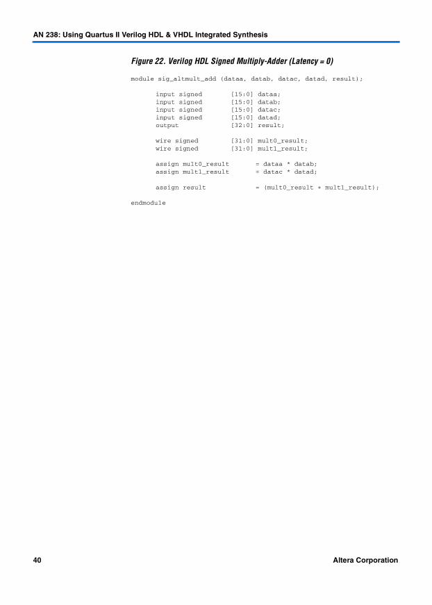
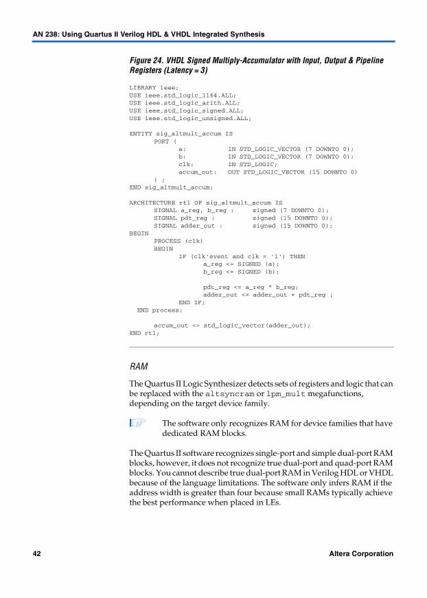
Multiply-Accumulators & Multiply-Adders
The Quartus II Logic Synthesizer finds multiply-accumulators or multiply-adders and converts them to altmult_accum or altmult_add megafunctions, respectively. The software then places these functions in DSP blocks.
1 The software only supports inference for these functions if the target device family has dedicated DSP blocks.
A multiply-accumulator consists of a multiply operator feeding an addition operator. The addition operator feeds a set of registers that then feed the second input to the addition operator. A multiply-adder consists of two to four multiply operators feeding one or two levels of addition, subtraction, or addition/subtraction operators. The second-level operator, if used, is always addition. In addition to the multiply-accumulator and multiply-adder, the Quartus II Fitter can also place input and output registers into the DSP block (i.e., perform register packing) to improve performance and LE utilization.
f For more information on the DSP block and the functions it implements, refer to the appropriate device family data sheet and the DSP Solutions Center on the Altera web site at http://www.altera.com.
38 Altera Corporation

AN 238: Using Quartus II Verilog HDL & VHDL Integrated Synthesis
The Quartus II Assignment Organizer and Assignment Editor contain an option for Individual Nodes & Entities, called Auto DSP Block Replacement, that you can use to control DSP block inference. This option is turned on by default. To disable inference, turn off this option for your whole project or for a specific block.
Figures 21 and 22 show Verilog HDL and VHDL examples of inference for particular multiply-accumulators and multiply-adders.
Figure 21. Verilog HDL Unsigned Multiply-Accumulator with Input, Output & Pipeline Registers (Latency = 3)
module unsig_altmult_accum (dataout, dataa, datab, clk, aclr, clken);
input [7:0] dataa;input [7:0] datab;input clk;input aclr;input clken;
output [31:0] dataout;
reg [31:0] dataout;reg [7:0] dataa_reg;reg [7:0] datab_reg;reg [15:0] multa_reg;
wire [15:0] multa;wire [31:0] adder_out;
assign multa = dataa_reg * datab_reg;assign adder_out = multa_reg + dataout;
always @(posedge clk or posedge aclr)begin
if(aclr)begin
dataa_reg <= 0;datab_reg <= 0;
multa_reg <= 0;
dataout <= 0;end
else if(clken)begin
dataa_reg <= dataa;datab_reg <= datab;
multa_reg <= multa;
dataout <= adder_out;end
end
endmodule
Altera Corporation 39
AN 238: Using Quartus II Verilog HDL & VHDL Integrated Synthesis
Figure 22. Verilog HDL Signed Multiply-Adder (Latency = 0)
module sig_altmult_add (dataa, datab, datac, datad, result);
input signed [15:0] dataa;input signed [15:0] datab;input signed [15:0] datac;input signed [15:0] datad;output [32:0] result;
wire signed [31:0] mult0_result;wire signed [31:0] mult1_result;
assign mult0_result = dataa * datab;assign mult1_result = datac * datad;
assign result = (mult0_result + mult1_result);
endmodule
40 Altera Corporation

AN 238: Using Quartus II Verilog HDL & VHDL Integrated Synthesis
Figure 23. VHDL Unsigned Multiply-Adder with Input, Output & Pipeline Registers (Latency = 3)’LIBRARY ieee;USE ieee.std_logic_1164.ALL;USE ieee.std_logic_arith.ALL;USE ieee.std_logic_signed.ALL;USE ieee.std_logic_unsigned.ALL;
ENTITY unsignedmult_add ISPORT (
a: IN STD_LOGIC_VECTOR (7 DOWNTO 0);b: IN STD_LOGIC_VECTOR (7 DOWNTO 0);c: IN STD_LOGIC_VECTOR (7 DOWNTO 0);d: IN STD_LOGIC_VECTOR (7 DOWNTO 0);clk : IN STD_LOGIC;aclr : IN STD_LOGIC;result: OUT STD_LOGIC_VECTOR (15 DOWNTO 0)
);END unsignedmult_add;
ARCHITECTURE rtl OF unsignedmult_add ISSIGNAL a_int, b_int, c_int, d_int : STD_LOGIC_VECTOR (7 DOWNTO 0);SIGNAL pdt_int, pdt2_int: unsigned (15 DOWNTO 0);SIGNAL result_int: unsigned (15 DOWNTO 0);
BEGINPROCESS (clk, aclr)BEGIN
IF (aclr = '1') THENa_int <= (OTHERS => '0');b_int <= (OTHERS => '0');c_int <= (OTHERS => '0');d_int <= (OTHERS => '0');pdt_int <= (OTHERS => '0');pdt2_int <= (OTHERS => '0');result_int <= (OTHERS => '0');
ELSIF (clk'event AND clk = '1') THENa_int <= a; b_int <= b; c_int <= c;d_int <= d;
pdt_int <= unsigned(a_int) * unsigned(b_int);pdt2_int <= unsigned(c_int) * unsigned(d_int);result_int <= pdt_int + pdt2_int;
END IF;END PROCESS;
result <= STD_LOGIC_VECTOR(result_int); END rtl;
Altera Corporation 41
AN 238: Using Quartus II Verilog HDL & VHDL Integrated Synthesis
Figure 24. VHDL Signed Multiply-Accumulator with Input, Output & Pipeline Registers (Latency = 3)’LIBRARY ieee;USE ieee.std_logic_1164.ALL;USE ieee.std_logic_arith.ALL;USE ieee.std_logic_signed.ALL;USE ieee.std_logic_unsigned.ALL;
ENTITY sig_altmult_accum ISPORT (
a: IN STD_LOGIC_VECTOR (7 DOWNTO 0);b: IN STD_LOGIC_VECTOR (7 DOWNTO 0);clk: IN STD_LOGIC;accum_out: OUT STD_LOGIC_VECTOR (15 DOWNTO 0)
) ;END sig_altmult_accum;
ARCHITECTURE rtl OF sig_altmult_accum ISSIGNAL a_reg, b_reg : signed (7 DOWNTO 0);SIGNAL pdt_reg : signed (15 DOWNTO 0);SIGNAL adder_out : signed (15 DOWNTO 0);
BEGINPROCESS (clk) BEGIN
IF (clk'event and clk = '1') THENa_reg <= SIGNED (a);b_reg <= SIGNED (b);
pdt_reg <= a_reg * b_reg;adder_out <= adder_out + pdt_reg ;
END IF; END process;
accum_out <= std_logic_vector(adder_out);END rtl;
RAM
The Quartus II Logic Synthesizer detects sets of registers and logic that can be replaced with the altsyncram or lpm_mult megafunctions, depending on the target device family.
1 The software only recognizes RAM for device families that have dedicated RAM blocks.
The Quartus II software recognizes single-port and simple dual-port RAM blocks, however, it does not recognize true dual-port and quad-port RAM blocks. You cannot describe true dual-port RAM in Verilog HDL or VHDL because of the language limitations. The software only infers RAM if the address width is greater than four because small RAMs typically achieve the best performance when placed in LEs.
42 Altera Corporation

AN 238: Using Quartus II Verilog HDL & VHDL Integrated Synthesis
1 For simple dual-port RAM with separate read and write clocks, using a RAM megafunction changes the design functionality slightly if the RAM reads from and writes to the same location. In these cases, the software issues a warning and Quartus II Help explains the condition under which the functionality changes.
The Quartus II Assignment Organizer and Assignment Editor contain an option for Individual Nodes & Entities, called Auto RAM Replacement, that you can use to control RAM inference. This option is turned on by default. To disable inference, turn off this option for your whole project or for a specific block.
1 The Quartus II software can require significantly more than Altera’s recommended memory requirements to infer large amounts of RAM, potentially causing runtime compilation problems. Designs with more than 100 Kbits of inferred memory may not compile successfully due to these issues. Altera recommends that you do not infer large memories, such as those targeting Stratix M-RAM blocks, in the Quartus II software. Instead, use the altsyncram megafunction.
Figures 25 through 28 show Verilog HDL and VHDL examples that infer single- and dual-clock synchronous RAM. Depending on the device family’s dedicated RAM architecture, the RAM may or may not have to be synchronous; consult the device family data sheet for details.
Figures 29 and 30 show Verilog HDL and VHDL examples of RAM with asynchronous read addresses but registered outputs. The implementation of these RAM examples varies depending on the dedicated RAM architecture of your target device family. For example, in an APEX device this RAM is straightforward to implement because the APEX architecture supports asynchronous read addresses.
For Stratix devices, read addresses must be registered, therefore, you cannot directly implement these examples. To implement the code in the Stratix architecture by inferring an altsyncram megafunction, the Quartus II Compiler moves the output registers to the inputs of the RAM. This movement changes the functionality slightly, so the software issues a warning and Quartus II Help explains the differences.
For the dual-clock examples, the functionality of the inferred megafunction differs from the original HDL code if you are reading and writing to the same address (the Compiler issues a warning to inform you of this functional difference).
Altera Corporation 43

AN 238: Using Quartus II Verilog HDL & VHDL Integrated Synthesis
Figure 25. Verilog HDL Single-Clock Synchronous RAM
module ram_infer(q, a, d, we, clk); output[7:0] q; input [7:0] d; input [6:0] a; input we, clk; reg [7:0] q; reg [6:0] read_add; reg [7:0] mem [127:0];
always @(posedge clk) begin if (we) mem[a] <= d; read_add <= a; end
assign q = mem[read_add];endmodule
Figure 26. Verilog HDL Dual-Clock Synchronous RAM
module ram_dual(q, addr_in, addr_out, d, we, clk1, clk2);output[7:0] q;input [7:0] d;input [6:0] addr_in;input [6:0] addr_out;input we, clk1, clk2;
reg [6:0] addr_out_reg;reg [7:0] q;reg [7:0] mem [127:0];
always @(posedge clk1)begin
if (we)mem[addr_in] <= d;
end
always @(posedge clk2) beginq <= mem[addr_out_reg];addr_out_reg <= addr_out;
endendmodule
44 Altera Corporation

AN 238: Using Quartus II Verilog HDL & VHDL Integrated Synthesis
Figure 27. VHDL Single-Clock Synchronous RAM’LIBRARY ieee;USE ieee.std_logic_1164.ALL;
ENTITY ram ISPORT(
clock: IN STD_LOGIC;data: IN STD_LOGIC_VECTOR (2 DOWNTO 0);write_address: IN integer RANGE 0 to 31;read_address: IN integer RANGE 0 to 31;we: IN std_logic;q: OUT STD_LOGIC_VECTOR (2 DOWNTO 0)
);END ram;
ARCHITECTURE rtl OF ram ISTYPE MEM IS ARRAY(0 TO 31) OF std_logic_vector(2 DOWNTO 0);
SIGNAL ram_block : MEM;SIGNAL read_address_reg : integer RANGE 0 to 31;
BEGINPROCESS (clock)BEGIN
IF (clock'event AND clock = '1') THENIF (we = '1') THEN
ram_block(write_address) <= data;END IF;
read_address_reg <= read_address;
END IF;END PROCESS;
q <= ram_block(read_address_reg);
END rtl;
Altera Corporation 45

AN 238: Using Quartus II Verilog HDL & VHDL Integrated Synthesis
Figure 28. VHDL Dual-Clock Synchronous RAM’LIBRARY ieee;USE ieee.std_logic_1164.ALL;
ENTITY ram_dual ISPORT(
clock1, clock2: IN STD_LOGIC;data: IN STD_LOGIC_VECTOR (3 DOWNTO 0);write_address: IN integer RANGE 0 to 1023;read_address: IN integer RANGE 0 to 1023;we: IN std_logic;q: OUT STD_LOGIC_VECTOR (3 DOWNTO 0)
);END ram_dual;
ARCHITECTURE rtl OF ram_dual ISTYPE MEM IS ARRAY(0 TO 31) OF std_logic_vector(3 DOWNTO 0);
SIGNAL ram_block : MEM;SIGNAL read_address_reg : integer RANGE 0 to 1023;
BEGINPROCESS (clock1)BEGIN
IF (clock1'event AND clock1 = '1') THENIF (we = '1') THEN
ram_block(write_address) <= data;END IF;
END IF;END PROCESS;
PROCESS (clock2)BEGIN
IF (clock2'event AND clock2 = '1') THENq <= ram_block(read_address_reg);read_address_reg <= read_address;
END IF;END PROCESS;
END rtl;
46 Altera Corporation
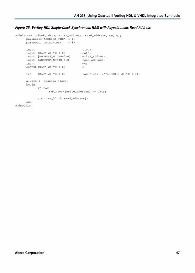
AN 238: Using Quartus II Verilog HDL & VHDL Integrated Synthesis
Figure 29. Verilog HDL Single-Clock Synchronous RAM with Asynchronous Read Address
module ram (clock, data, write_address, read_address, we, q);parameter ADDRESS_WIDTH = 4;parameter DATA_WIDTH = 8;
input clock;input [DATA_WIDTH-1:0] data;input [ADDRESS_WIDTH-1:0] write_address;input [ADDRESS_WIDTH-1:0] read_address;input we;output [DATA_WIDTH-1:0] q;
reg [DATA_WIDTH-1:0] ram_block [2**ADDRESS_WIDTH-1:0];
always @ (posedge clock)begin
if (we)ram_block[write_address] <= data;
q <= ram_block[read_address];end
endmodule
Altera Corporation 47

AN 238: Using Quartus II Verilog HDL & VHDL Integrated Synthesis
Figure 30. VHDL Single-Clock Synchronous RAM with Asynchronous Read Address
LIBRARY ieee;USE ieee.std_logic_1164.ALL;USE ieee.numeric_std.ALL;
ENTITY ram ISGENERIC(
ADDRESS_WIDTH: integer := 4;DATA_WIDTH: integer := 8
);PORT(
clock : IN std_logic;data : IN std_logic_vector(DATA_WIDTH - 1 DOWNTO 0);write_address : IN std_logic_vector(ADDRESS_WIDTH - 1 DOWNTO 0);read_address : IN std_logic_vector(ADDRESS_WIDTH - 1 DOWNTO 0);we : IN std_logic;q : OUT std_logic_vector(DATA_WIDTH - 1 DOWNTO 0)
);END ram;
ARCHITECTURE rtl OF ram ISTYPE RAM IS ARRAY(0 TO 2 ** ADDRESS_WIDTH - 1) OF std_logic_vector(DATA_WIDTH - 1 DOWNTO 0);
SIGNAL ram_block : RAM;BEGIN
PROCESS (clock)BEGIN
IF (clock’event AND clock = ’1’) THENIF (we = ’1’) THEN ram_block(to_integer(unsigned(write_address))) <= data;END IF;
q <= ram_block(to_integer(unsigned(read_address)));END IF;
END PROCESS;END rtl;
Shift Registers
The Quartus II Logic Synthesizer detects a group of shift registers of the same length and converts them to an altshift_taps megafunction. To be detected, the shift registers must all use the same clock and clock enable, must not have any other secondary signals, and must have equally spaced taps that are at least three registers apart. The software only recognizes shift registers for device families that have dedicated RAM.
For FLEX and ACEX devices, the software does not infer altshift_taps because these devices have a relatively small amount of dedicated memory.
48 Altera Corporation

AN 238: Using Quartus II Verilog HDL & VHDL Integrated Synthesis
For APEX devices, the software infers altshift_taps if the shift register has more than a total of 128 bits. Smaller shift registers typically do not benefit from implementation in dedicated memory.
For Stratix and Cyclone™ devices, the software decides to infer the function based on the width of the register bus (W), the length between each tap (L) and the number of taps (N).
■ If the register bus width is one (W = 1), the software infers altshift_taps if the number of taps times the length between each tap is greater than or equal to 64 (N × L ≥ 64).
■ If the register bus width is greater than one (W > 1), the software infers altshift_taps if the register bus width times the number of taps times the length between each tap is greater than or equal to 32 (W × N × L ≥ 32).
1 The software uses more LEs to decode the read and write counters if the length between each tap (L) is not a power of 2. This situation occurs because for different sizes of shift register, external decode logic (using LEs) is required to implement the function, eliminating the advantage of implementing the shift register in memory.
The Quartus II Assignment Organizer and Assignment Editor contain an option for Individual Nodes & Entities, called Auto Shift Register Replacement, that you can use to control shift register inference. This option is turned on by default. To disable inference, turn off this option for your whole project or for a specific block.
1 The registers that the software maps to the altshift_taps megafunction and places in RAM are not available in the Simulator because their node names do not exist after synthesis.
Figure 31 shows a Verilog HDL example of a simple, single-bit wide, 64-bit long shift register. The software implements this single-bit register (W = 1 and M ≥ 64) in an altshift_taps megafunction for Stratix devices. If the length of the register were less than 64 bits, the software would implement this shift register in LEs.
Altera Corporation 49

AN 238: Using Quartus II Verilog HDL & VHDL Integrated Synthesis
Figure 31. Verilog HDL Single-Bit Wide, 64-Bit Long Shift Register’module shift_1x64 (clk,
shift,sr_in,sr_out,
);
input clk, shift;input sr_in;output sr_out;
reg [63:0] sr;
always@(posedge clk)begin
if (shift == 1'b1)begin
sr[63:1] <= sr[62:0];sr[0] <= sr_in;
endend
assign sr_out = sr[63];
endmodule
Figure 32 shows a Verilog HDL example of an 8-bit wide, 64-bit long shift register (W > 1 and M ≥ 64) with evenly spaced taps at 15, 31, and 47. The software implements this function in a single altshift_taps megafunction and maps it to RAM in Stratix and Cyclone devices.
50 Altera Corporation
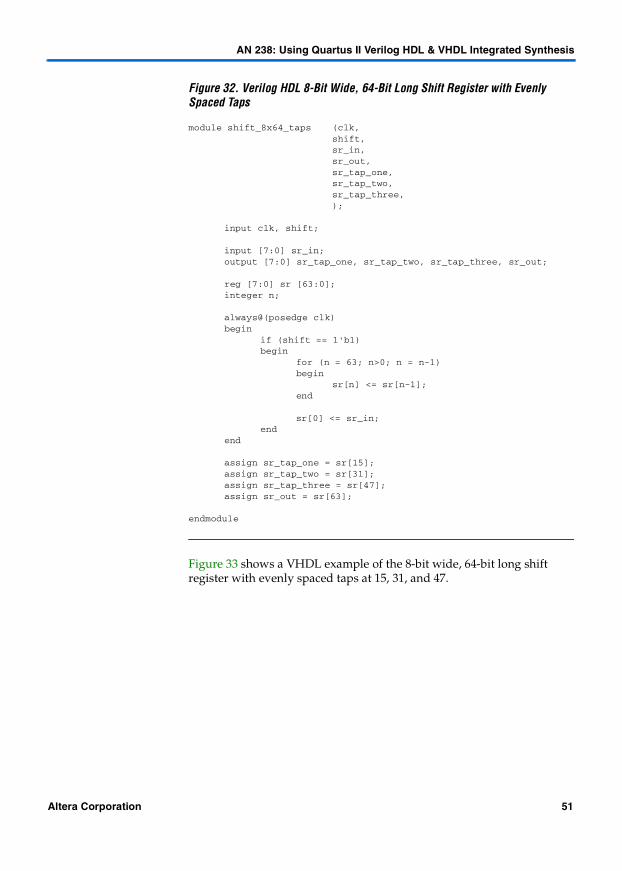
AN 238: Using Quartus II Verilog HDL & VHDL Integrated Synthesis
Figure 32. Verilog HDL 8-Bit Wide, 64-Bit Long Shift Register with Evenly Spaced Taps’module shift_8x64_taps (clk,
shift,sr_in,sr_out,sr_tap_one,sr_tap_two,sr_tap_three,
);
input clk, shift;
input [7:0] sr_in;output [7:0] sr_tap_one, sr_tap_two, sr_tap_three, sr_out;
reg [7:0] sr [63:0];integer n;
always@(posedge clk)begin
if (shift == 1'b1)begin
for (n = 63; n>0; n = n-1)begin
sr[n] <= sr[n-1];end
sr[0] <= sr_in;end
end
assign sr_tap_one = sr[15];assign sr_tap_two = sr[31];assign sr_tap_three = sr[47];assign sr_out = sr[63];
endmodule
Figure 33 shows a VHDL example of the 8-bit wide, 64-bit long shift register with evenly spaced taps at 15, 31, and 47.
Altera Corporation 51

AN 238: Using Quartus II Verilog HDL & VHDL Integrated Synthesis
Figure 33. VHDL 8-Bit Wide, 64-Bit Long Shift Register with Evenly Spaced Taps’LIBRARY IEEE;USE IEEE.STD_LOGIC_1164.ALL;
ENTITY shift_8x64_taps ISPORT (
clk : IN STD_LOGIC;shift : IN STD_LOGIC;sr_in : IN STD_LOGIC_VECTOR(7 DOWNTO 0);sr_tap_one : OUT STD_LOGIC_VECTOR(7 DOWNTO 0);sr_tap_two : OUT STD_LOGIC_VECTOR(7 DOWNTO 0);sr_tap_three : OUT STD_LOGIC_VECTOR(7 DOWNTO 0);sr_out : OUT STD_LOGIC_VECTOR(7 DOWNTO 0)
);END shift_8x64_taps;
ARCHITECTURE arch OF shift_8x64_taps IS
SUBTYPE sr_width IS STD_LOGIC_VECTOR(7 DOWNTO 0);TYPE sr_length IS ARRAY (63 DOWNTO 0) OF sr_width;
SIGNAL sr : sr_length;
BEGINPROCESS (clk)BEGIN
IF (clk'EVENT and clk = '1') THENIF (shift = '1') THEN
sr(63 DOWNTO 1) <= sr(62 DOWNTO 0);sr(0) <= sr_in;
END IF;END IF;
END PROCESS;
sr_tap_one <= sr(15);sr_tap_two <= sr(31);sr_tap_three <= sr(47);sr_out <= sr(63);
END arch;
52 Altera Corporation

AN 238: Using Quartus II Verilog HDL & VHDL Integrated Synthesis
Conclusion The Quartus II software includes complete Verilog HDL and VHDL language support, making it a complete easy-to-use standalone solution for SOPC designs. This document describes design methodologies and coding style guidelines that you can use to improve synthesis results and obtain optimum performance in your target Altera device.
Revision History
The information contained in AN 238: Using Quartus II Verilog HDL & VHDL Integrated Synthesis version 1.2 supersedes information published in previous versions.
Version 1.2
This version of the document contains the following changes:
■ Added “Compiler Directives” on page 4■ Added “Attributes” on page 4■ Updated the information in “Quartus II Logic Options” on page 5.■ Made minor text updates throughout the document.
Version 1.1
This version of the document contains the following changes:
■ Updated text on page 49.■ Updated text on page 50.
Copyright © 2002 Altera Corporation. All rights reserved. Altera, The Programmable Solutions Company, thestylized Altera logo, specific device designations, and all other words and logos that are identified astrademarks and/or service marks are, unless noted otherwise, the trademarks and service marks of AlteraCorporation in the U.S. and other countries. All other product or service names are the property of theirrespective holders. Altera products are protected under numerous U.S. and foreign patents and pendingapplications, mask work rights, and copyrights. Altera warrants performance of itssemiconductor products to current specifications in accordance with Altera’s standardwarranty, but reserves the right to make changes to any products and services at any timewithout notice. Altera assumes no responsibility or liability arising out of the applicationor use of any information, product, or service described herein except as expressly agreedto in writing by Altera Corporation. Altera customers are advised to obtain the latestversion of device specifications before relying on any published information and beforeplacing orders for products or services.
53 Altera Corporation
101 Innovation DriveSan Jose, CA 95134(408) 544-7000http://www.altera.comApplications Hotline:(800) 800-EPLDLiterature Services:[email protected]