
AN #201: Interfacing to an ISU Digital Inclinometer...
20
Page 1 of 20 AN #201: Interfacing to an ISU Module Application Note AN #201: Interfacing to an ISU Digital Inclinometer Module 1 - Introduction The ISU series of Single-Axis Digital Inclinometers from STT are self-contained, ready to use circuit modules which provide real-time digital measurements of angular displacement through a full 360 degree range. The units can be used in a wide variety of applications, accept a standard 5 Volt DC supply, and provide both RS-232 and PWM outputs. In addition, the RS-232 serial interface can be used to configure the device for the purpose of enabling or disabling various features. A basic functional block diagram of the device is provided in Figure 1 below. Figure 1-ISU Functional Block Diagram 2 - Electrical Connections Pin Descriptions VDD – This is the 5 Volt power supply input for both the analog and digital sections of the ISU Module. The power supply must be sufficient to provide a maximum of 2mA of current during normal operation. This connection is referenced with the “+” notation as shown on the physical module layout in Figure 2. GND – This is the ground input for the ISU Module. This connection is referenced with the “-” notation as shown on the physical module layout in Figure 2. ! "#$# % &#%’ ISU Functional Block Diagram (!##) *%’" &% &#’%" %+## %#%’ ! "#$# % &#%’ ISU Functional Block Diagram (!##) *%’" &% &#’%" %+## %#%’ (!##) *%’" &% &#’%" %+## %#%’
-
Upload
nguyenliem -
Category
Documents
-
view
214 -
download
2
Transcript of AN #201: Interfacing to an ISU Digital Inclinometer...

Page 1 of 20 AN #201: Interfacing to an ISU Module
Application Note
AN #201: Interfacing to an ISU Digital Inclinometer Module 1 - Introduction
The ISU series of Single-Axis Digital Inclinometers from STT are self-contained, ready to use circuit modules which provide real-time digital measurements of angular displacement through a full 360 degree range. The units can be used in a wide variety of applications, accept a standard 5 Volt DC supply, and provide both RS-232 and PWM outputs. In addition, the RS-232 serial interface can be used to configure the device for the purpose of enabling or disabling various features.
A basic functional block diagram of the device is provided in Figure 1 below.
Figure 1-ISU Functional Block Diagram
2 - Electrical Connections
Pin Descriptions
VDD – This is the 5 Volt power supply input for both the analog and digital sections of the ISU Module. The power supply must be sufficient to provide a maximum of 2mA of current during normal operation. This connection is referenced with the “+” notation as shown on the physical module layout in Figure 2.
GND – This is the ground input for the ISU Module. This connection is referenced with the “-” notation as shown on the physical module layout in Figure 2.
������
��� �
��
������
���
��
�����
� ���������
� !����� "#$� �#�%&���#%'�
ISU FunctionalBlock Diagram
� ( !#�#)�*%'"�&�%���
&#'% "��%+#�#�%#%'
������
������ ��
����
������ ������
������
����
����������
� ���������
� !����� "#$� �#�%&���#%'�
ISU FunctionalBlock Diagram
� ( !#�#)�*%'"�&�%���
&#'% "��%+#�#�%#%'
� ( !#�#)�*%'"�&�%���
&#'% "��%+#�#�%#%'
Page 2 of 20 AN #201: Interfacing to an ISU Module
Application Note
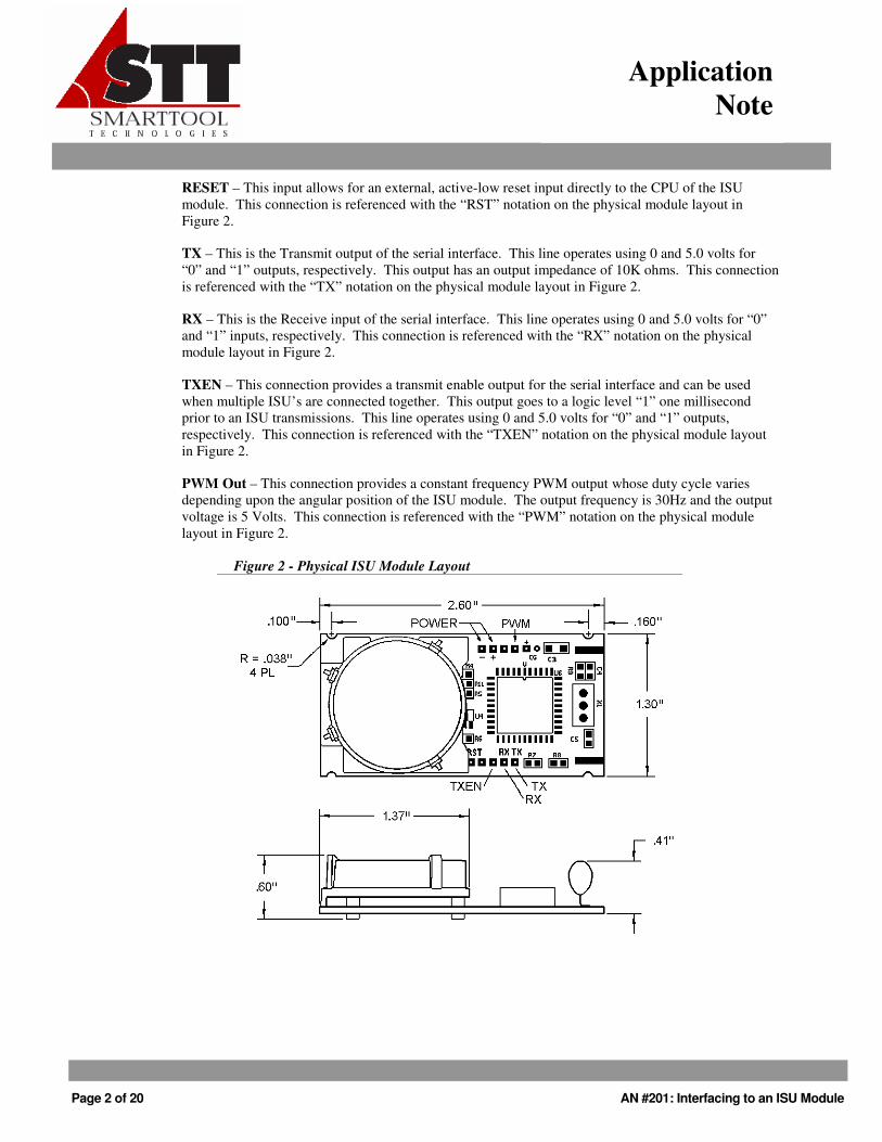
RESET – This input allows for an external, active-low reset input directly to the CPU of the ISU module. This connection is referenced with the “RST” notation on the physical module layout in Figure 2.
TX – This is the Transmit output of the serial interface. This line operates using 0 and 5.0 volts for “0” and “1” outputs, respectively. This output has an output impedance of 10K ohms. This connection is referenced with the “TX” notation on the physical module layout in Figure 2.
RX – This is the Receive input of the serial interface. This line operates using 0 and 5.0 volts for “0” and “1” inputs, respectively. This connection is referenced with the “RX” notation on the physical module layout in Figure 2.
TXEN – This connection provides a transmit enable output for the serial interface and can be used when multiple ISU’s are connected together. This output goes to a logic level “1” one millisecond prior to an ISU transmissions. This line operates using 0 and 5.0 volts for “0” and “1” outputs, respectively. This connection is referenced with the “TXEN” notation on the physical module layout in Figure 2.
PWM Out – This connection provides a constant frequency PWM output whose duty cycle varies depending upon the angular position of the ISU module. The output frequency is 30Hz and the output voltage is 5 Volts. This connection is referenced with the “PWM” notation on the physical module layout in Figure 2.
Figure 2 - Physical ISU Module Layout
Page 3 of 20 AN #201: Interfacing to an ISU Module
Application Note
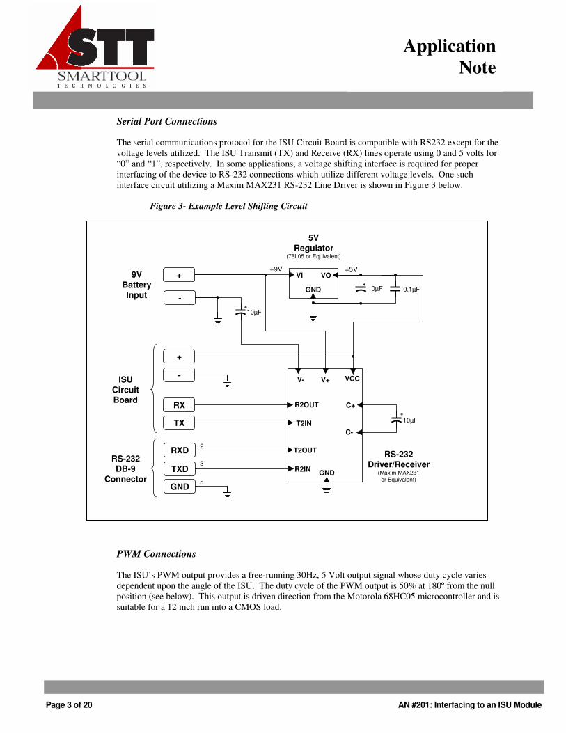
Serial Port Connections
The serial communications protocol for the ISU Circuit Board is compatible with RS232 except for the voltage levels utilized. The ISU Transmit (TX) and Receive (RX) lines operate using 0 and 5 volts for “0” and “1”, respectively. In some applications, a voltage shifting interface is required for proper interfacing of the device to RS-232 connections which utilize different voltage levels. One such interface circuit utilizing a Maxim MAX231 RS-232 Line Driver is shown in Figure 3 below.
Figure 3- Example Level Shifting Circuit
PWM Connections
The ISU’s PWM output provides a free-running 30Hz, 5 Volt output signal whose duty cycle varies dependent upon the angle of the ISU. The duty cycle of the PWM output is 50% at 180º from the null position (see below). This output is driven direction from the Motorola 68HC05 microcontroller and is suitable for a 12 inch run into a CMOS load.
V+
GND
RXD
TXD
GND
RX
TX
-
+
T2OUT
R2IN
R2OUT
T2IN
VCC
-
+ VI VO
GND
+
V-
C+
C-
+
+
+9V +5V
2
9VBatteryInput
ISUCircuitBoard
RS-232DB-9
Connector
3
5
5VRegulator
(78L05 or Equivalent)
RS-232Driver/Receiver
(Maxim MAX231or Equivalent)
10µF
10µF
10µF
0.1µF

Page 4 of 20 AN #201: Interfacing to an ISU Module
Application Note
3 - Physical to Angular Position Referencing
The ISU Inclinometer module provides angle measurement output through the full 360° range. This output will vary from 0° to 359.99° referenced from a null position. This null position defaults to the physical, zero degree position as shown in Figure 4 below, but can be changed via the serial interface.
Figure 4 - Default Null Position
Rotating the module clockwise from the null position causes the angle output from the ISU module to change from 0° to 359.99° as shown in Figure 5 below.
Figure 5 - Clockwise Rotation from Null Position
Default Null Position (0°)Default Null Position (0°)
ISUModule
DefaultNull Position(0 Degrees)
90°Position
180°Position
270°Position
ISU
Module
ISUModule
ISU
Mod
ule
ISUModuleISUModule
DefaultNull Position(0 Degrees)
90°Position
180°Position
270°Position
ISU
Module
ISU
Module
ISUModuleISUModule
ISU
Mod
ule
ISU
Mod
ule
Page 5 of 20 AN #201: Interfacing to an ISU Module
Application Note
4 - Serial Port Interface Protocol
Overview
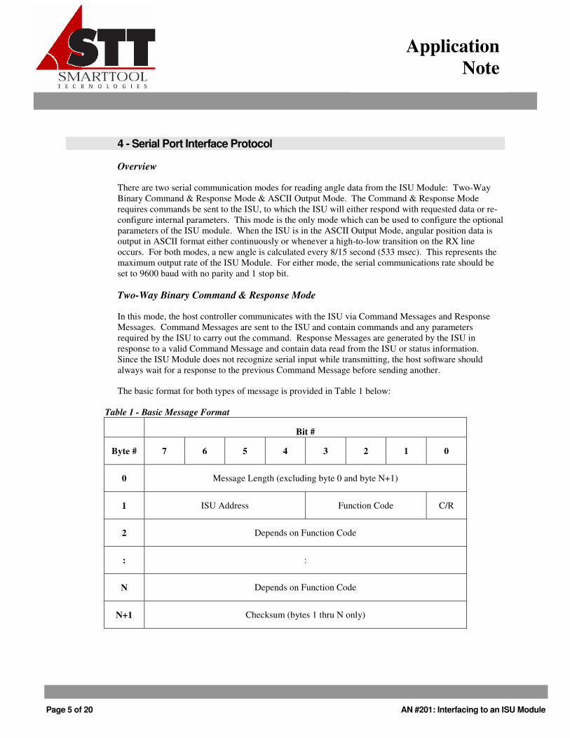
There are two serial communication modes for reading angle data from the ISU Module: Two-Way Binary Command & Response Mode & ASCII Output Mode. The Command & Response Mode requires commands be sent to the ISU, to which the ISU will either respond with requested data or re-configure internal parameters. This mode is the only mode which can be used to configure the optional parameters of the ISU module. When the ISU is in the ASCII Output Mode, angular position data is output in ASCII format either continuously or whenever a high-to-low transition on the RX line occurs. For both modes, a new angle is calculated every 8/15 second (533 msec). This represents the maximum output rate of the ISU Module. For either mode, the serial communications rate should be set to 9600 baud with no parity and 1 stop bit.
Two-Way Binary Command & Response Mode
In this mode, the host controller communicates with the ISU via Command Messages and Response Messages. Command Messages are sent to the ISU and contain commands and any parameters required by the ISU to carry out the command. Response Messages are generated by the ISU in response to a valid Command Message and contain data read from the ISU or status information. Since the ISU Module does not recognize serial input while transmitting, the host software should always wait for a response to the previous Command Message before sending another.
The basic format for both types of message is provided in Table 1 below:
Table 1 - Basic Message Format
Bit #
Byte # 7 6 5 4 3 2 1 0
0 Message Length (excluding byte 0 and byte N+1)
1 ISU Address Function Code C/R
2 Depends on Function Code
: :
N Depends on Function Code
N+1 Checksum (bytes 1 thru N only)

Page 6 of 20 AN #201: Interfacing to an ISU Module
Application Note
Message Length – This field contains the number of bytes in the message, exclusive of the first and last bytes.
ISU Address – Up to 14 ISU’s may be interfaced together on a single serial port for party line operation. These 4 bits specify the address of the ISU to which the command is addressed. ALL ISU’s will respond to address 0 such that, for party line configurations, the only valid addresses are 1-14 (address 15 is reserved). The address of an ISU is stored in EEPROM and can be changed by the host. Details of how to modify the address of an ISU are provided later.
Function Code – There are seven valid function codes, as listed in Table 2 below.
Table 2 - Function Codes Function Code Bits
Bit 3 Bit 2 Bit 1 Description
0 0 0 Go To Soft Error State
0 0 1 Reset Module
0 1 0 Read RAM
0 1 1 Write RAM
1 0 0 Read EEPROM
1 0 1 Write EEPROM
1 1 0 Reset Null Point
C/R – This bit identifies whether the particular message is a Command message or a Response message. This bit should be set to 0 for Commands sent to an ISU and will be set to 1 for Responses from the ISU to the host.
The ISU recognizes four categories of errors in Command and Response mode, each of which is described below.
Command Timeout
While receiving messages on the serial port, the ISU software is continually checking for commands with valid function code and length pairs. If the length doesn’t match the function code, the software assumes an overrun condition occurred. The module will continue to read and test length/function code pairs until a valid pair is found or until a serial timeout occurs. A serial timeout occurs if received messages do not complete within 400 msecs.

Page 7 of 20 AN #201: Interfacing to an ISU Module
Application Note
Invalid Function Code
If a message is received with an invalid function code, the module will respond back with the following error response message:
Invalid Function Code Response Message
Byte #
0 01H
1 FFH
2 FFH
Invalid Checksum
If a message is received with an invalid checksum in the last byte, the module will respond back with the following error response message:
Invalid Function Code Response Message
Byte #
0 01H
1 FDH
2 FDH
Module is in Error State
During operation and at power-up, the module is constantly monitoring itself for hardware error conditions. Examples of hardware error conditions include a corrupted EEPROM or an invalid angle reading. If an error condition is detected, the module will enter into the Hard Error state. While in the Hard Error state, the module will not calculate angle values and will respond to serial commands with the following error response message:
Hardware Error State Response Message
Byte #
0 02H
1 F1H
2 Function Code from Initial Command Message
3 Checksum (Bytes 1 & 2 only)
The module will enter into the Soft Error state following a successful “Go To Soft Error State” Function Command Message. While in the Soft Error state, the serial port will respond normally to all commands but will still not calculate angle values.
A more detailed description of each of the Function Codes and the expected Response messages is provided in Appendix A.

Page 8 of 20 AN #201: Interfacing to an ISU Module
Application Note
ASCII Output Mode
In the ASCII Output mode, the angular position of the ISU module is output in ASCII format depending upon the state of the RX line. If the RX line is held low (0 volts) when power is applied (or upon a reset condition) and it remains low, the angular position of the module will be output every 533 msec. If the RX line is held high (5 Volts) when power is applied (or upon a reset condition), the angular position of the module will be output upon a high-to-low (1 to 0) transition on the RX line, provided that the RX line remains low for at least 100msec. As mentioned above, the ASCII output rate will not exceed once every 533 msec.
The angular position will be output as 9 ASCII characters in the following format:
{sign}XXX.XX{carriage return}{line feed}
Examples:
+124.50 + 32.70 + 9.38
- 4.31 -179.99
5 - PWM Interface Protocol
The ISU’s PWM output provides a free-running (no trigger) 30Hz, 5 Volt output signal whose duty cycle varies dependent upon the angle of the ISU. The duty cycle output varies over 4096 steps with each step representing 4.34µsec. The duty cycle of the PWM output is a minimum of 23.33% at the null position and 50% at +180° from the null position.
The duty cycle can be translated to an angular position with the following equation:
Angle = 6.749*[Duty Cycle in %] – 157.45°
Example:
A duty cycle of 36.6% is measured. The angle is equal to
= 6.749 *36.6 – 157.45°
= 247.01 - 157.45°
= 89.56 degrees

Page 9 of 20 AN #201: Interfacing to an ISU Module
Application Note
6 - Programming the ISU Module
Programming the ISU Module consists simply of reading desired data values, i.e., angle readings or option settings, from RAM or EEPROM and reading and writing EEPROM values to enable or disable desired features. This is accomplished via the dedicated function codes discussed earlier. This section will outline how data is organized in RAM and EEPROM locations as well as list the relevant data locations for all information available to the user. The data described in these address locations is the ONLY data that should be changed by the user. Modification of other data will most likely render the module inoperable and irreparable.
RAM Organization
The ISU Module’s RAM is organized into 16-bit words which are accessed via the Read and Write RAM function codes. Data is returned most significant byte (MSB) first.
The relevant data locations for all information available to the user is listed in Table 3 below.
Table 3- Available RAM Addresses
Address # of
Bytes Description Usage
58H 2 Current Angle
(High Byte First)
[Angle High Byte *256 + Angle Low Byte] * 360/65536 will yield the current angle reading in degrees.
EEPROM Organization
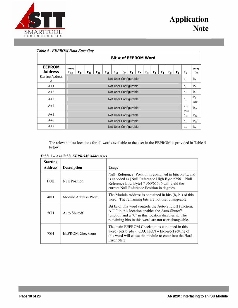
The ISU Module’s EEPROM is arranged into 256 16-bit words which are accessed via the Read and Write EEPROM function codes. The relevant EEPROM data available to the user is encoded as a 16-bit ‘data’ word into the lower 2 bits of 8 consecutive EEPROM words and must be ‘decoded’ prior to use. Table 4 below demonstrates the encoding of these user accessible data words (b15-b0) into the 16 lower two bits of 8 consecutive EEPROM words (E15-E0).
Page 10 of 20 AN #201: Interfacing to an ISU Module
Application Note
Table 4 - EEPROM Data Encoding
,#��-��.��� �������+�
�� ����*++�����
��&,��
�/�� �/0� �/1� �/2� �//� �/�� �3� ��� �4� ��� ��� �0� �1� �2� �/�
�5&,��
���
��������������
� ��������������������� ��� ���
��� ��������������������� ��� ���
��� ��������������������� ��� ���
��� ��������������������� ������
��� !�
��� ���������������������
����
�"� !�����
��� ��������������������� ���� ����
��� ��������������������� ���� ����
��� ��������������������� �#� �$�
The relevant data locations for all words available to the user in the EEPROM is provided in Table 5 below:
Table 5 – Available EEPROM Addressses Starting Address Description Usage
D0H Null Position
Null ‘Reference’ Position is contained in bits b15-b0 and is encoded as [Null Reference High Byte *256 + Null Reference Low Byte] * 360/65536 will yield the current Null Reference Position in degrees.
48H Module Address Word The Module Address is contained in bits (b7-b4) of this word. The remaining bits are not user changeable.
50H Auto Shutoff
Bit b0 of this word controls the Auto-Shutoff function. A “1” in this location enables the Auto-Shutoff function and a “0” in this location disables it. The remaining bits in this word are not user changeable.
78H EEPROM Checksum
The main EEPROM Checksum is contained in this word (bits b15-b0). CAUTION – Incorrect setting of this word will cause the module to enter into the Hard Error State.

Page 11 of 20 AN #201: Interfacing to an ISU Module
Application Note
EEPROM Checksum
Whenever programmable values are changed in the EEPROM, the EEPROM checksum MUST be updated to avoid the module entering the Hard Error State. This checksum is the lower 16 bits of the binary sum of all 256 EEPROM Words and is encoded into EEPROM addresses 78H-7FH as shown in Table 4 above. Failure to properly update the checksum will result in the unit entering the Hard Error state and will render the unit inoperable until the checksum is corrected.

Page 12 of 20 AN #201: Interfacing to an ISU Module
Application Note
7 - Programming Examples
This section will provide command programming examples of the most commonly used functions. If some programming is required but is beyond the scope of the user, STT provides a free software program which can be used to perform all of these functions. This program, ST.EXE, is available for download directly from our website.
Reading an Angle Value
To request an angle reading, simply issue a 2-byte Read RAM command of address 58H of the ISU. To do this, send the following 5 bytes to the ISU (assuming the ISU address is 00H):
Byte # Value Description 0 03H Length = 3 1 04H Read RAM Function Code
(Command) 2 58H Address = 58H 3 02H Read 2 Bytes 4 5EH Checksum of bytes 1-3
The ISU will then respond with the following 6 bytes:
Byte # Value Description 0 04H Length = 4 1 05H Read RAM Function Code
(Response) 2 58H Address = 58H 3 DB1 Angle High Byte 4 DB0 Angle Low Byte 5 Checksum Checksum of bytes 1-4
The angle reading is calculated from DB1 & DB0 as follows:
Angle (in degrees) = [DB1 *256 + DB0] * 360/65536

Page 13 of 20 AN #201: Interfacing to an ISU Module
Application Note
Setting an Alternate Null Reference Point
As mentioned in Section 3, the ISU module comes with the Null Reference point set by default to the position shown in Figure 5. The default Null position can be set to the current angular position via the Reset Null Position function code. To issue the command, send the following 3 bytes to the ISU (assuming the ISU address is 00H):
Byte # Value Description 0 01H Length = 1 1 0CH Reset Null Position
Function Code (Command) 2 OCH Checksum
The ISU will then respond with the following 3 bytes:
Byte # Value Description 0 01H Length = 1 1 0DH Reset Null Position
Function Code (Response) 2 0DH Checksum
Setting the Module Address
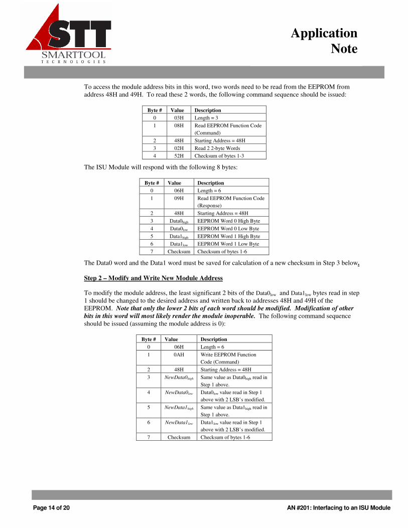
Multiple ISU Modules can be utilized on the same serial bus via the addressing scheme discussed in Section 4. All modules come configured from the factory as address 0, to which any ISU responds. Addresses in a multi-ISU configuration can range from 1 to 14, with address 15 being reserved. The module address is encoded into bits b7-b4 of the 16-bit encoded Module Address Word starting at address 48H (see Table 5). Modifying this address consists of (1) reading the 16-bit encoded word starting at address 48H; (2) Modifying bits b7-b4 and writing the modified, encoded word back into the EEPROM; and (3) Reading, modifying, and updating the EEPROM checksum. The command sequence for doing this is provided below:
Step 1 – Read Word Containing the Module Address
The Module Address Word begins at address 48H with the bits encoded as follows:
Address Data Word Bits 48H b7,b6
49H b5,b4 4AH b3,b2 4BH b1,b0 4CH b15,b14 4DH b13,b12 4EH b11,b10 4FH b9,b8
Page 14 of 20 AN #201: Interfacing to an ISU Module
Application Note
To access the module address bits in this word, two words need to be read from the EEPROM from address 48H and 49H. To read these 2 words, the following command sequence should be issued:
Byte # Value Description 0 03H Length = 3 1 08H Read EEPROM Function Code
(Command) 2 48H Starting Address = 48H 3 02H Read 2 2-byte Words 4 52H Checksum of bytes 1-3
The ISU Module will respond with the following 8 bytes:
Byte # Value Description 0 06H Length = 6 1 09H Read EEPROM Function Code
(Response) 2 48H Starting Address = 48H 3 Data0high EEPROM Word 0 High Byte 4 Data0low EEPROM Word 0 Low Byte 5 Data1high EEPROM Word 1 High Byte 6 Data1low EEPROM Word 1 Low Byte 7 Checksum Checksum of bytes 1-6
The Data0 word and the Data1 word must be saved for calculation of a new checksum in Step 3 below.
Step 2 – Modify and Write New Module Address
To modify the module address, the least significant 2 bits of the Data0low and Data1low bytes read in step 1 should be changed to the desired address and written back to addresses 48H and 49H of the EEPROM. Note that only the lower 2 bits of each word should be modified. Modification of other bits in this word will most likely render the module inoperable. The following command sequence should be issued (assuming the module address is 0):
Byte # Value Description 0 06H Length = 6 1 0AH Write EEPROM Function
Code (Command) 2 48H Starting Address = 48H 3 NewData0high Same value as Data0high read in
Step 1 above. 4 NewData0low Data0low value read in Step 1
above with 2 LSB’s modified. 5 NewData1high Same value as Data1high read in
Step 1 above. 6 NewData1low Data1low value read in Step 1
above with 2 LSB’s modified. 7 Checksum Checksum of bytes 1-6
Page 15 of 20 AN #201: Interfacing to an ISU Module
Application Note
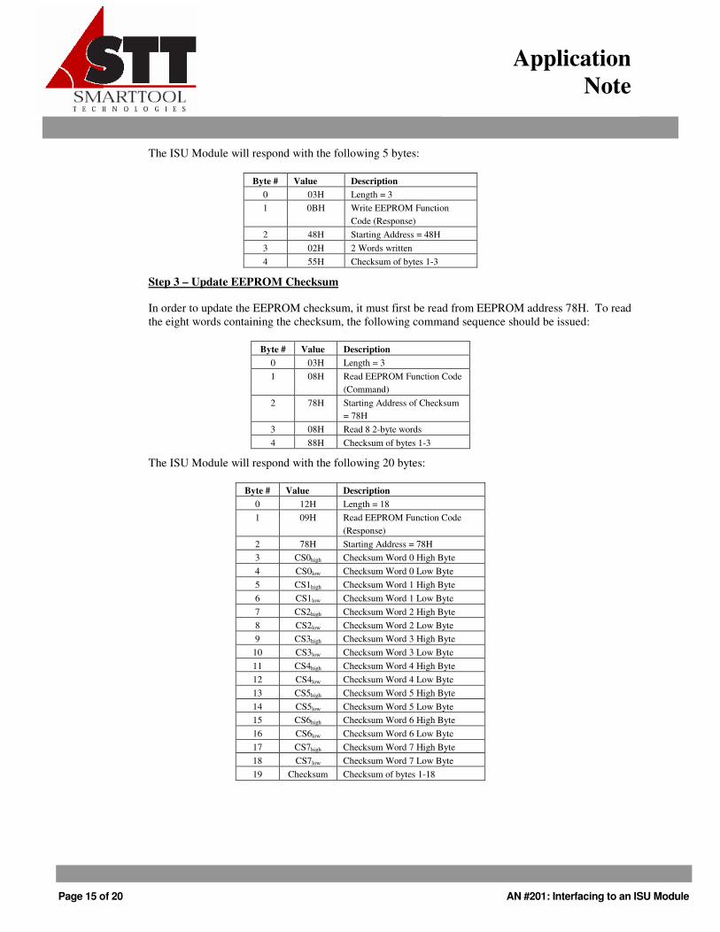
The ISU Module will respond with the following 5 bytes:
Byte # Value Description 0 03H Length = 3 1 0BH Write EEPROM Function
Code (Response) 2 48H Starting Address = 48H 3 02H 2 Words written 4 55H Checksum of bytes 1-3
Step 3 – Update EEPROM Checksum
In order to update the EEPROM checksum, it must first be read from EEPROM address 78H. To read the eight words containing the checksum, the following command sequence should be issued:
Byte # Value Description 0 03H Length = 3 1 08H Read EEPROM Function Code
(Command) 2 78H Starting Address of Checksum
= 78H 3 08H Read 8 2-byte words 4 88H Checksum of bytes 1-3
The ISU Module will respond with the following 20 bytes:
Byte # Value Description 0 12H Length = 18 1 09H Read EEPROM Function Code
(Response) 2 78H Starting Address = 78H 3 CS0high Checksum Word 0 High Byte 4 CS0low Checksum Word 0 Low Byte 5 CS1high Checksum Word 1 High Byte 6 CS1low Checksum Word 1 Low Byte 7 CS2high Checksum Word 2 High Byte 8 CS2low Checksum Word 2 Low Byte 9 CS3high Checksum Word 3 High Byte
10 CS3low Checksum Word 3 Low Byte 11 CS4high Checksum Word 4 High Byte 12 CS4low Checksum Word 4 Low Byte 13 CS5high Checksum Word 5 High Byte 14 CS5low Checksum Word 5 Low Byte 15 CS6high Checksum Word 6 High Byte 16 CS6low Checksum Word 6 Low Byte 17 CS7high Checksum Word 7 High Byte 18 CS7low Checksum Word 7 Low Byte 19 Checksum Checksum of bytes 1-18

Page 16 of 20 AN #201: Interfacing to an ISU Module
Application Note
The checksum value should be decoded from words CS0-CS7 as described in Table 4 above. The new checksum should be calculated as follows:
New Checksum = Old Checksum - Data0 - Data1 + NewData0 + NewData1
Where Data0 and Data1 are the original Data0 and Data1 words read from the EEPROM in step 1.
Once the New Checksum is determined, it should be encoded into the lower 2 bits of 8 new data words (NewCS0-NewCS7) without modifying the upper 14 bits of the original data words. Once the new words are determined, they should be written to the EEPROM with the following sequence.
Byte # Value Description 0 12H Length = 18 1 0AH Write EEPROM Function Code (Command) 2 78H Starting Address = 78H 3 NewCS0high EEPROM Word 0 High Byte (Modified) 4 NewCS0low EEPROM Word 0 Low Byte (Modified) 5 NewCS1high EEPROM Word 1 High Byte (Modified) 6 NewCS1low EEPROM Word 1 Low Byte (Modified) 7 NewCS2high EEPROM Word 2 High Byte (Modified) 8 NewCS2low EEPROM Word 2 Low Byte (Modified) 9 NewCS3high EEPROM Word 3 High Byte (Modified)
10 NewCS3low EEPROM Word 3 Low Byte (Modified) 11 NewCS4high EEPROM Word 4 High Byte (Modified) 12 NewCS4low EEPROM Word 4 Low Byte (Modified) 13 NewCS5high EEPROM Word 5 High Byte (Modified) 14 NewCS5low EEPROM Word 5 Low Byte (Modified) 15 NewCS6high EEPROM Word 6 High Byte (Modified) 16 NewCS6low EEPROM Word 6 Low Byte (Modified) 17 NewCS7high EEPROM Word 7 High Byte (Modified) 18 NewCS7low EEPROM Word 7 Low Byte (Modified) 19 Checksum Checksum of bytes 1-18
The ISU Module will respond with the following 5 bytes:
Byte # Value Description 0 03H Length = 3 1 0BH Write EEPROM Function
Code (Response) 2 78H Starting Address = 78H 3 08H 8 Words written 4 8BH Checksum of bytes 1-3

Page 17 of 20 AN #201: Interfacing to an ISU Module
Application Note
Appendix A – Function Code Reference
Function Code 000 – Go To Soft Error State
Description:
Causes the module to enter into the Soft Error state from the Hard Error state. If not in the Hard error state, this command has no effect.
Message Formats:
Command Message Response Message
Bit # Bit #
Byte # 7 6 5 4 3 2 1 0 Byte # 7 6 5 4 3 2 1 0
0 01H 0 01H
1 ISU Address 0 0 0 0 1 ISU Address 0 0 0 1
2 Checksum (same as byte 1) 2 Checksum (same as byte 1)
Function Code 001 – Reset Module
Description:
This function is used to reset the module and cause the equivalent of a power-on reset.
Message Formats:
Command Message Response Message
Bit # Bit #
Byte # 7 6 5 4 3 2 1 0 Byte # 7 6 5 4 3 2 1 0
0 01H 0 01H
1 ISU Address 0 0 1 0 1 ISU Address 0 0 1 1
2 Checksum (same as Byte 1) 2 Checksum (same as Byte 1)
Page 18 of 20 AN #201: Interfacing to an ISU Module
Application Note
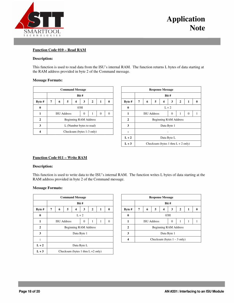
Function Code 010 – Read RAM
Description:
This function is used to read data from the ISU’s internal RAM. The function returns L bytes of data starting at the RAM address provided in byte 2 of the Command message.
Message Formats:
Command Message Response Message
Bit # Bit #
Byte # 7 6 5 4 3 2 1 0 Byte # 7 6 5 4 3 2 1 0
0 03H 0 L + 2
1 ISU Address 0 1 0 0 1 ISU Address 0 1 0 1
2 Beginning RAM Address 2 Beginning RAM Address
3 L (Number bytes to read) 3 Data Byte 1
4 Checksum (bytes 1-3 only) : :
L + 2 Data Byte L
L + 3 Checksum (bytes 1 thru L + 2 only)
Function Code 011 – Write RAM
Description:
This function is used to write data to the ISU’s internal RAM. The function writes L bytes of data starting at the RAM address provided in byte 2 of the Command message.
Message Formats:
Command Message Response Message
Bit # Bit #
Byte # 7 6 5 4 3 2 1 0 Byte # 7 6 5 4 3 2 1 0
0 L + 2 0 03H
1 ISU Address 0 1 1 0 1 ISU Address 0 1 1 1
2 Beginning RAM Address 2 Beginning RAM Address
3 Data Byte 1 3 Data Byte 1
: : 4 Checksum (bytes 1 – 3 only)
L + 2 Data Byte L
L + 3 Checksum (bytes 1 thru L +2 only)
Page 19 of 20 AN #201: Interfacing to an ISU Module
Application Note
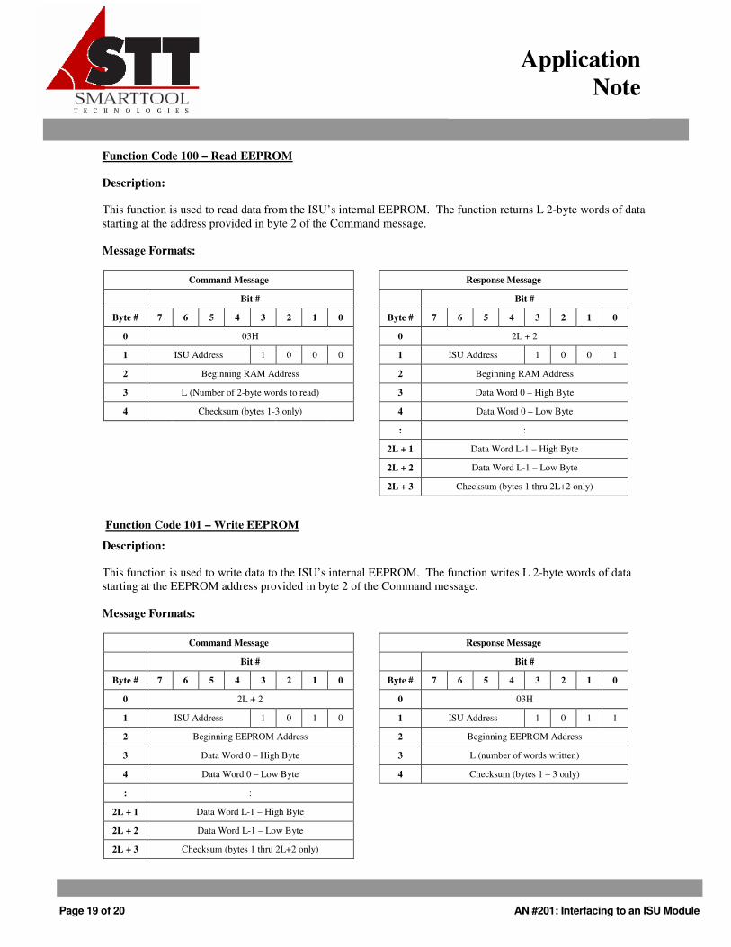
Function Code 100 – Read EEPROM
Description:
This function is used to read data from the ISU’s internal EEPROM. The function returns L 2-byte words of data starting at the address provided in byte 2 of the Command message.
Message Formats:
Command Message Response Message
Bit # Bit #
Byte # 7 6 5 4 3 2 1 0 Byte # 7 6 5 4 3 2 1 0
0 03H 0 2L + 2
1 ISU Address 1 0 0 0 1 ISU Address 1 0 0 1
2 Beginning RAM Address 2 Beginning RAM Address
3 L (Number of 2-byte words to read) 3 Data Word 0 – High Byte
4 Checksum (bytes 1-3 only) 4 Data Word 0 – Low Byte
: :
2L + 1 Data Word L-1 – High Byte
2L + 2 Data Word L-1 – Low Byte
2L + 3 Checksum (bytes 1 thru 2L+2 only)
Function Code 101 – Write EEPROM
Description:
This function is used to write data to the ISU’s internal EEPROM. The function writes L 2-byte words of data starting at the EEPROM address provided in byte 2 of the Command message.
Message Formats:
Command Message Response Message
Bit # Bit #
Byte # 7 6 5 4 3 2 1 0 Byte # 7 6 5 4 3 2 1 0
0 2L + 2 0 03H
1 ISU Address 1 0 1 0 1 ISU Address 1 0 1 1
2 Beginning EEPROM Address 2 Beginning EEPROM Address
3 Data Word 0 – High Byte 3 L (number of words written)
4 Data Word 0 – Low Byte 4 Checksum (bytes 1 – 3 only)
: :
2L + 1 Data Word L-1 – High Byte
2L + 2 Data Word L-1 – Low Byte
2L + 3 Checksum (bytes 1 thru 2L+2 only)
Page 20 of 20 AN #201: Interfacing to an ISU Module
Application Note
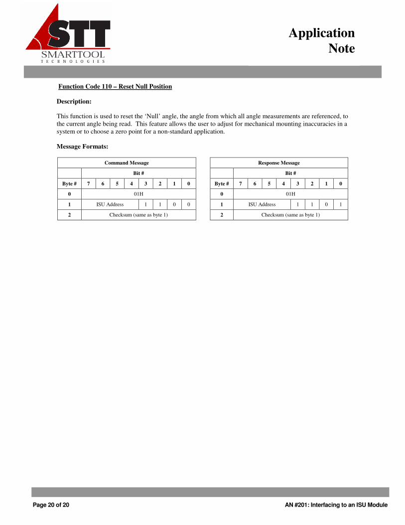
Function Code 110 – Reset Null Position
Description:
This function is used to reset the ‘Null’ angle, the angle from which all angle measurements are referenced, to the current angle being read. This feature allows the user to adjust for mechanical mounting inaccuracies in a system or to choose a zero point for a non-standard application.
Message Formats:
Command Message Response Message
Bit # Bit #
Byte # 7 6 5 4 3 2 1 0 Byte # 7 6 5 4 3 2 1 0
0 01H 0 01H
1 ISU Address 1 1 0 0 1 ISU Address 1 1 0 1
2 Checksum (same as byte 1) 2 Checksum (same as byte 1)