AN-100 - TDK | Attracting Tomorrow MEMS Microphone Handling and Assembly Guide InvenSense reserves...
13
AN-100 MEMS Microphone Handling and Assembly Guide InvenSense reserves the right to change the detail specifications as may be required to permit improvements in the design of its products. InvenSense Inc. 1745 Technology Drive, San Jose, CA 95110 U.S.A +1(408) 988–7339 www.invensense.com Document Number: AN-100-00 Revision: 1.3 Release Date: 12/10/2015 PURPOSE AND SCOPE This document provides information and general guidelines for handling and assembling boards with InvenSense Micro Electro- Mechanical Systems (MEMS) microphones. REFLOW SOLDERING AND BOARD ASSEMBLY PRINTING PARAMETERS The recommended solder paste printing parameters are Print pressure = 3 kg Print speed = 30 mm/sec Squeegee type = metal Squeegee angle = 60° SOLDER PASTE STENCIL PARAMETERS The solder paste stencil parameters are Stencil type = laser cut Stencil thickness = 3 mils (~75 μm) SUGGESTED SOLDER PASTE The suggested solder paste is Indium8.9 (Type 4—alloy composition—96.5Sn/3.0Ag/0.5Cu (SAC305)). This paste is an air reflow, no- clean solder paste specifically formulated to accommodate the higher processing temperatures required by the Sn/Ag/Cu, Sn/Ag, and other alloy systems favored by the electronics industry to replace conventional Pb-bearing solders. PLACEMENT FORCE MEMS microphones can be handled using standard pick-and-place and chip shooting equipment. Care should be taken to avoid damage to the MEMS microphone structure as follows: Use a standard pickup tool to handle the microphone. On bottom-port microphones where the hole is on the bottom of the package, the pickup tool can make contact with any part of the lid surface. The size of the pickup tool should be no smaller than the size of the package. This will prevent denting of the lid during mounting. Do not pick up the microphone with a vacuum tool that makes contact with the microphone’s sound port. Do not pull air out of or blow air into the microphone port. Do not use excessive force (>1 kg) to place the microphone on the PCB. REFLOW PROFILE InvenSense products are qualified in accordance with IPC/JEDEC J-STD-020D.1. This standard classifies proper packaging, storage and handling in order to avoid subsequent thermal and mechanical damage during the solder-reflow attachment phase of PCB assembly. The qualification preconditioning process specifies a sequence consisting of a bake cycle, a moisture soak cycle (in a temperature humidity oven), and three consecutive solder reflow cycles, followed by functional device testing. The peak solder reflow classification temperature requirement for package qualification is (260°C +0°C/-5°C) for lead-free soldering of components measuring less than 1.6 mm in thickness. The qualification profile and a table explaining the set points are shown below. The reflow profile in Figure 1 is recommended for board manufacturing with InvenSense MEMS microphones. These microphones are also compatible with the profile described in J-STD-020D.1.
Transcript of AN-100 - TDK | Attracting Tomorrow MEMS Microphone Handling and Assembly Guide InvenSense reserves...
AN-100
MEMS Microphone Handling and Assembly Guide
InvenSense reserves the right to change the detail specifications as may be required to permit improvements
in the design of its products.
InvenSense Inc. 1745 Technology Drive, San Jose, CA 95110 U.S.A
+1(408) 988–7339 www.invensense.com
Document Number: AN-100-00 Revision: 1.3 Release Date: 12/10/2015
PURPOSE AND SCOPE This document provides information and general guidelines for handling and assembling boards with InvenSense Micro Electro-Mechanical Systems (MEMS) microphones.
REFLOW SOLDERING AND BOARD ASSEMBLY
PRINTING PARAMETERS The recommended solder paste printing parameters are
Print pressure = 3 kg
Print speed = 30 mm/sec
Squeegee type = metal
Squeegee angle = 60°
SOLDER PASTE STENCIL PARAMETERS The solder paste stencil parameters are
Stencil type = laser cut
Stencil thickness = 3 mils (~75 µm)
SUGGESTED SOLDER PASTE The suggested solder paste is Indium8.9 (Type 4—alloy composition—96.5Sn/3.0Ag/0.5Cu (SAC305)). This paste is an air reflow, no-clean solder paste specifically formulated to accommodate the higher processing temperatures required by the Sn/Ag/Cu, Sn/Ag, and other alloy systems favored by the electronics industry to replace conventional Pb-bearing solders.
PLACEMENT FORCE MEMS microphones can be handled using standard pick-and-place and chip shooting equipment. Care should be taken to avoid damage to the MEMS microphone structure as follows:
Use a standard pickup tool to handle the microphone. On bottom-port microphones where the hole is on the bottom of the package, the pickup tool can make contact with any part of the lid surface.
The size of the pickup tool should be no smaller than the size of the package. This will prevent denting of the lid during mounting.
Do not pick up the microphone with a vacuum tool that makes contact with the microphone’s sound port. Do not pull air out of or blow air into the microphone port.
Do not use excessive force (>1 kg) to place the microphone on the PCB.
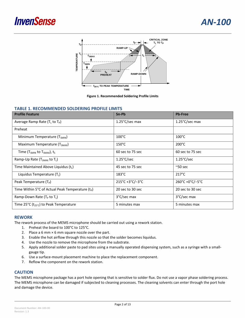
REFLOW PROFILE InvenSense products are qualified in accordance with IPC/JEDEC J-STD-020D.1. This standard classifies proper packaging, storage and handling in order to avoid subsequent thermal and mechanical damage during the solder-reflow attachment phase of PCB assembly. The qualification preconditioning process specifies a sequence consisting of a bake cycle, a moisture soak cycle (in a temperature humidity oven), and three consecutive solder reflow cycles, followed by functional device testing. The peak solder reflow classification temperature requirement for package qualification is (260°C +0°C/-5°C) for lead-free soldering of components measuring less than 1.6 mm in thickness. The qualification profile and a table explaining the set points are shown below. The reflow profile in Figure 1 is recommended for board manufacturing with InvenSense MEMS microphones. These microphones are also compatible with the profile described in J-STD-020D.1.
AN-100
Page 2 of 13
Document Number: AN-100-00 Revision: 1.3
Figure 1. Recommended Soldering Profile Limits
TABLE 1. RECOMMENDED SOLDERING PROFILE LIMITS Profile Feature Sn-Pb Pb-Free
Average Ramp Rate (TL to TP) 1.25°C/sec max 1.25°C/sec max
Preheat
Minimum Temperature (TSMIN) 100°C 100°C
Maximum Temperature (TSMAX) 150°C 200°C
Time (TSMIN to TSMAX), tS 60 sec to 75 sec 60 sec to 75 sec
Ramp-Up Rate (TSMAX to TL) 1.25°C/sec 1.25°C/sec
Time Maintained Above Liquidus (tL) 45 sec to 75 sec ~50 sec
Liquidus Temperature (TL) 183°C 217°C
Peak Temperature (TP) 215°C +3°C/−3°C 260°C +0°C/−5°C
Time Within 5°C of Actual Peak Temperature (tP) 20 sec to 30 sec 20 sec to 30 sec
Ramp-Down Rate (TP to TL) 3°C/sec max 3°C/sec max
Time 25°C (t25°C) to Peak Temperature 5 minutes max 5 minutes max
REWORK The rework process of the MEMS microphone should be carried out using a rework station.
1. Preheat the board to 100°C to 125°C. 2. Place a 6 mm × 6 mm square nozzle over the part. 3. Enable the hot airflow through this nozzle so that the solder becomes liquidus. 4. Use the nozzle to remove the microphone from the substrate. 5. Apply additional solder paste to pad sites using a manually operated dispensing system, such as a syringe with a small-
gauge tip. 6. Use a surface-mount placement machine to place the replacement component. 7. Reflow the component on the rework station.
CAUTION The MEMS microphone package has a port hole opening that is sensitive to solder flux. Do not use a vapor phase soldering process. The MEMS microphone can be damaged if subjected to cleaning processes. The cleaning solvents can enter through the port hole and damage the device.
tP
tL
t25°C TO PEAK TEMPERATURE
tSPREHEAT
CRITICAL ZONE
TL TO TP
TE
MP
ER
AT
UR
E
TIME
RAMP-DOWN
RAMP-UP
TSMIN
TSMAX
TP
TL
AN-100
Page 3 of 13
Document Number: AN-100-00 Revision: 1.3
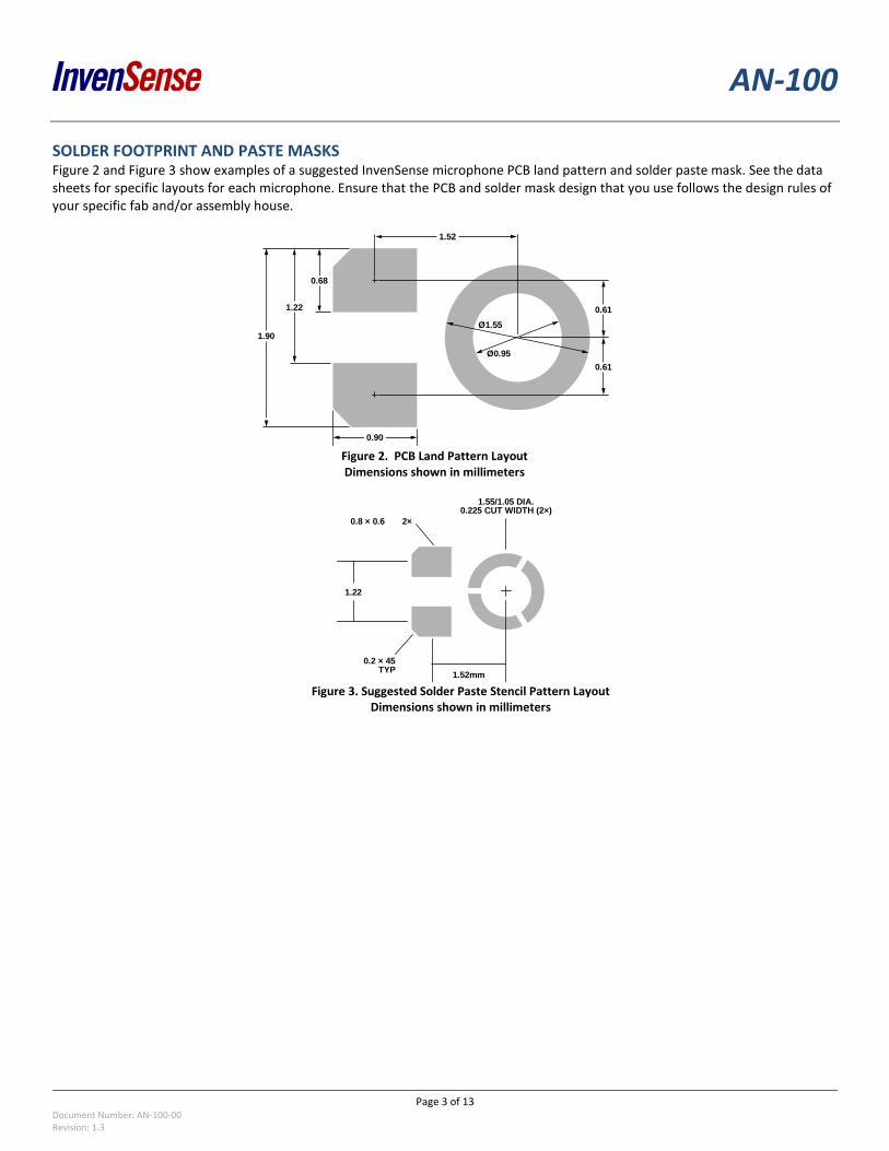
SOLDER FOOTPRINT AND PASTE MASKS Figure 2 and Figure 3 show examples of a suggested InvenSense microphone PCB land pattern and solder paste mask. See the data sheets for specific layouts for each microphone. Ensure that the PCB and solder mask design that you use follows the design rules of your specific fab and/or assembly house.
Figure 2. PCB Land Pattern Layout Dimensions shown in millimeters
Figure 3. Suggested Solder Paste Stencil Pattern Layout
Dimensions shown in millimeters
Ø1.55
Ø0.95
1.52
0.90
1.90
1.22
0.68
0.61
0.61
1.22
2×0.8 × 0.6
0.2 × 45TYP
1.52mm
1.55/1.05 DIA.0.225 CUT WIDTH (2×)
AN-100
Page 4 of 13
Document Number: AN-100-00 Revision: 1.3
HANDLING INSTRUCTIONS MEMS HANDING Unlike conventional IC products in similar packages, MEMS devices contain moving micromechanical structures. Therefore, MEMS devices require different handling precautions than conventional ICs prior to mounting onto PCBs.
InvenSense products have been qualified to a shock tolerance of 10,000g. Furthermore, the products are shipped in cushioned packaging to protect them from potential damage induced by normal handling and shipping.
Do not drop individually packaged sensors or reels of sensors.
PCBs that incorporate mounted sensors should not be separated by manually snapping apart. This could also create g-forces in excess of 10,000g.
Do not clean MEMS sensors in ultrasonic baths.
Do not open and remove MEMS devices from the moisture barrier bag until you are ready to use them. The moisture barrier bag provides good protection to the MEMS sensors during storage and transfer.
Devices dropped during handling should not be used.
ESD CONSIDERATIONS Establish and use ESD-safe handling precautions when unpacking and handling ESD-sensitive devices.
Store ESD sensitive devices in ESD safe containers until ready for use. The Tape-and-Reel moisture-sealed bag is an ESD approved barrier. The best practice is to keep the units in the original moisture sealed bags until ready for assembly.
Ensure that all workstations and personnel are properly grounded to prevent ESD. Contact InvenSense for the ESM-MM (Machine Model) rating of each individual microphone product. Restrict all device handling to ESD protected work areas that measure less than the static charge for the specific microphone’s rating.
STORAGE SPECIFICATIONS InvenSense products conform to the storage specifications of IPC/JEDEC J-STD-020D.1. The Moisture Sensitivity Level (MSL) of InvenSense microphones is shown in Table 2.
AN-100
Page 5 of 13
Document Number: AN-100-00 Revision: 1.3
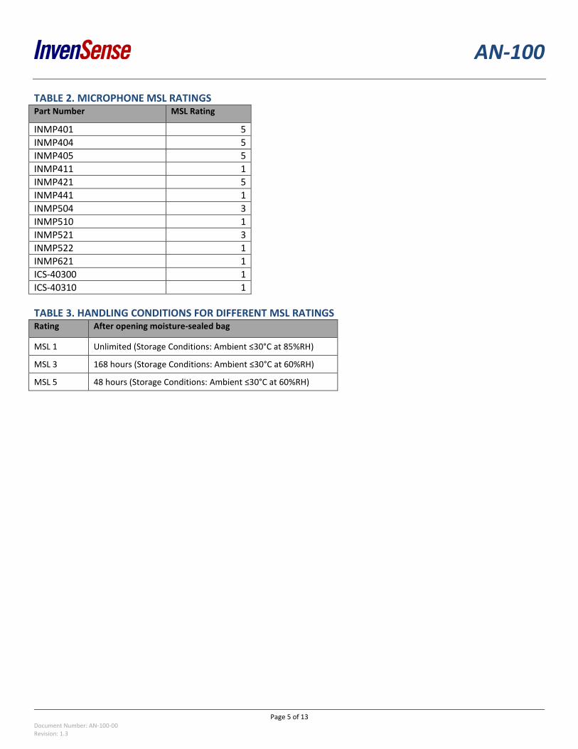
TABLE 2. MICROPHONE MSL RATINGS Part Number MSL Rating
INMP401 5
INMP404 5
INMP405 5
INMP411 1
INMP421 5
INMP441 1
INMP504 3
INMP510 1
INMP521 3
INMP522 1
INMP621 1
ICS-40300 1
ICS-40310 1
TABLE 3. HANDLING CONDITIONS FOR DIFFERENT MSL RATINGS Rating After opening moisture-sealed bag
MSL 1 Unlimited (Storage Conditions: Ambient ≤30°C at 85%RH)
MSL 3 168 hours (Storage Conditions: Ambient ≤30°C at 60%RH)
MSL 5 48 hours (Storage Conditions: Ambient ≤30°C at 60%RH)
AN-100
Page 6 of 13
Document Number: AN-100-00 Revision: 1.3
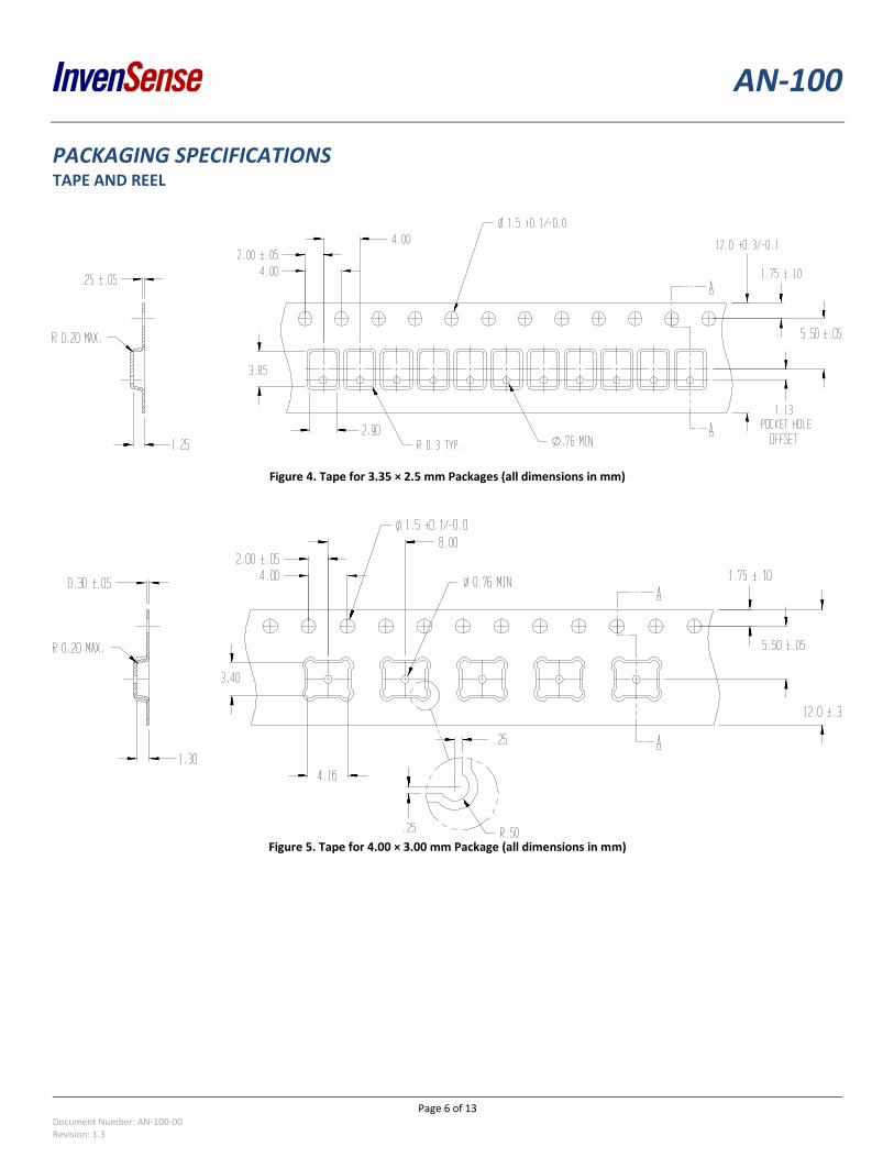
PACKAGING SPECIFICATIONS TAPE AND REEL
Figure 4. Tape for 3.35 × 2.5 mm Packages (all dimensions in mm)
Figure 5. Tape for 4.00 × 3.00 mm Package (all dimensions in mm)
AN-100
Page 7 of 13
Document Number: AN-100-00 Revision: 1.3
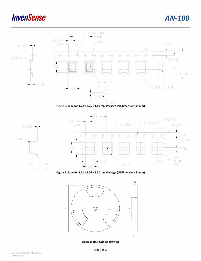
Figure 6. Tape for 4.72 × 3.76 × 1.00 mm Package (all dimensions in mm)
Figure 7. Tape for 4.72 × 3.76 × 3.50 mm Package (all dimensions in mm)
Figure 8. Reel Outline Drawing
AN-100
Page 8 of 13
Document Number: AN-100-00 Revision: 1.3
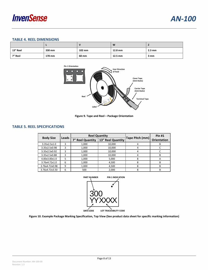
TABLE 4. REEL DIMENSIONS L V W Z
13” Reel 330 mm 102 mm 12.8 mm 2.3 mm
7” Reel 178 mm 68 mm 12.5 mm 3 mm
Figure 9. Tape and Reel – Package Orientation
TABLE 5. REEL SPECIFICATIONS
Body Size Leads Reel Quantity
Tape Pitch (mm) Pin #1
Orientation 7” Reel Quantity 13” Reel Quantity 3.35x2.5x1.0 3 1,000 10,000 4 B
3.35x2.5x0.98 3 1,000 10,000 4 C
3.35x2.5x0.92 3 1,000 10,000 4 C
3.35x2.5x0.88 3 1,000 10,000 4 B
4.00x3.00x1.0 5 1,000 5,000 8 A
3.76x4.72x1.0 6 1,000 4,500 8 B
3.76x4.72x0.98 9 1,000 4,500 8 B
3.76x4.72x3.50 6 500 2,000 8 B
Figure 10. Example Package Marking Specification, Top View (See product data sheet for specific marking information)
Label
Reel
Cover Tape (Anti-Static)
Carrier Tape (Anti-Static)
User Directionof Feed
Pin 1 Orientation
I n v e n S e n s e
Pb-
f
ree
c
a
teg
o
ry(e4)H F
DEVICE(1P
):MPU-6050PO:HUB
REELQTY(Q):5000
LOT1(1T):Q2R784-F1
D/C(D):1118
QTY(Q):3000
LOT2(1T):Q3V215-G1
D/C(D):1107
QTY(Q):2000
ReelDate:
18/05/11
QCSTAMP:
Terminal Tape
A
BC
YYXXXX300
LOT TRACEABILITY CODE
PIN 1 INDICATIONPART NUMBER
DATE CODE
AN-100
Page 9 of 13
Document Number: AN-100-00 Revision: 1.3
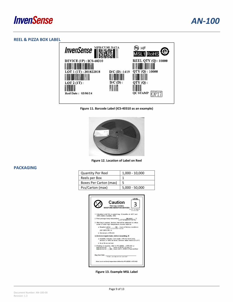
REEL & PIZZA BOX LABEL
Figure 11. Barcode Label (ICS-40310 as an example)
Figure 12. Location of Label on Reel
PACKAGING Quantity Per Reel 1,000 - 10,000
Reels per Box 1
Boxes Per Carton (max) 5
Pcs/Carton (max) 5,000 - 50,000
Figure 13. Example MSL Label
AN-100
Page 10 of 13
Document Number: AN-100-00 Revision: 1.3
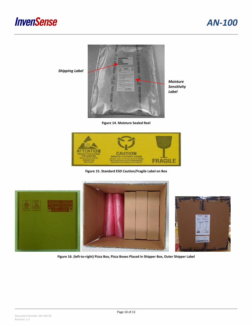
Figure 14. Moisture Sealed Reel
Figure 15. Standard ESD Caution/Fragile Label on Box
Figure 16. (left-to-right) Pizza Box, Pizza Boxes Placed in Shipper Box, Outer Shipper Label
Moisture Sensitivity Label
Shipping Label
AN-100
Page 11 of 13
Document Number: AN-100-00 Revision: 1.3
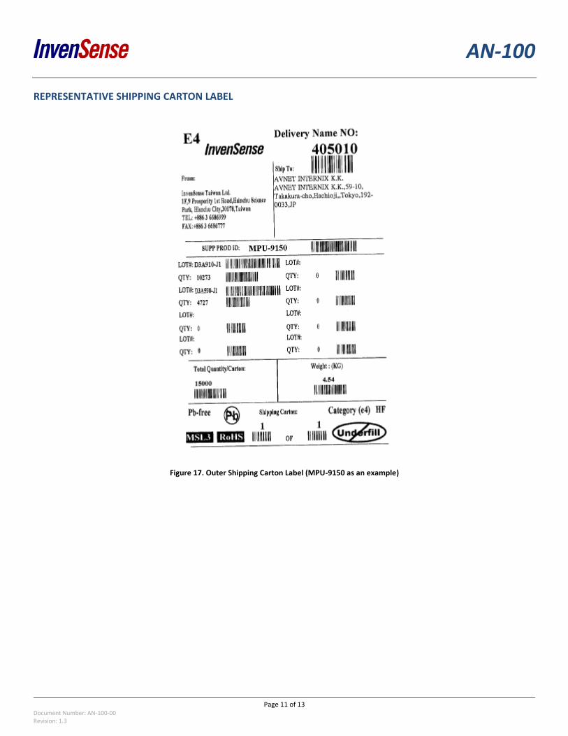
REPRESENTATIVE SHIPPING CARTON LABEL
Figure 17. Outer Shipping Carton Label (MPU-9150 as an example)
AN-100
Page 12 of 13
Document Number: AN-100-00 Revision: 1.3
REVISION HISTORY
REVISION DATE REVISION DESCRIPTION
7/14/2014 1.0 Initial Release
11/17/2014 1.1 Updated Table 3
11/06/2015 1.2 Updated Table 5
12/10/2015 1.3 Updated Table 4
AN-100
Page 13 of 13
Document Number: AN-100-00 Revision: 1.3
COMPLIANCE DECLARATION DISCLAIMER InvenSense believes the environmental and other compliance information given in this document to be correct but cannot guarantee accuracy or completeness. Conformity documents substantiating the specifications and component characteristics are on file. InvenSense subcontracts manufacturing, and the information contained herein is based on data received from vendors and suppliers, which has not been validated by InvenSense. This information furnished by InvenSense is believed to be accurate and reliable. However, no responsibility is assumed by InvenSense for its use, or for any infringements of patents or other rights of third parties that may result from its use. Specifications are subject to change without notice. InvenSense reserves the right to make changes to this product, including its circuits and software, in order to improve its design and/or performance, without prior notice. InvenSense makes no warranties, neither expressed nor implied, regarding the information and specifications contained in this document. InvenSense assumes no responsibility for any claims or damages arising from information contained in this document, or from the use of products and services detailed therein. This includes, but is not limited to, claims or damages based on the infringement of patents, copyrights, mask work and/or other intellectual property rights. Certain intellectual property owned by InvenSense and described in this document is patent protected. No license is granted by implication or otherwise under any patent or patent rights of InvenSense. This publication supersedes and replaces all information previously supplied. Trademarks that are registered trademarks are the property of their respective companies. InvenSense sensors should not be used or sold in the development, storage, production or utilization of any conventional or mass-destructive weapons or for any other weapons or life threatening applications, as well as in any other life critical applications such as medical equipment, transportation, aerospace and nuclear instruments, undersea equipment, power plant equipment, disaster prevention and crime prevention equipment. ©2015 InvenSense, Inc. All rights reserved. InvenSense, MotionTracking, MotionProcessing, MotionProcessor, MotionFusion, MotionApps, DMP, AAR and the InvenSense logo are trademarks of InvenSense, Inc. Other company and product names may be trademarks of the respective companies with which they are associated.
©2015 InvenSense, Inc. All rights reserved.