Amplitude Modulation - electronics-lab.info - Rootelectronics-lab.info/Files/CCE2310/Amplitude...
24
Amplitude Modulation
Transcript of Amplitude Modulation - electronics-lab.info - Rootelectronics-lab.info/Files/CCE2310/Amplitude...
Amplitude Modulation
© Joseph A. Zammit 2008 2
Table of contents Modulation theory .............................................................................................. 3
Amplitude modulation ....................................................................................... 4
Modulation Index .............................................................................................. 6
Power in an AM waveform ................................................................................ 9
Double Side Band – Suppressed Carrier ........................................................ 10
Single Sideband Modulation (SSB-AM) .......................................................... 10
Vestigial Sideband Amplitude Modulation (VSB – AM) ................................... 11
Appendix ........................................................................................................... 12
Practical AM modulators ................................................................................. 12
The chopper modulator ............................................................................... 12
Non linear devices ...................................................................................... 15
SSB generation ........................................................................................... 16
Integrated circuit modulators ....................................................................... 17
AM Demodulation techniques ......................................................................... 20
The diode detector ...................................................................................... 20
Synchronous AM detection ......................................................................... 22
Double Sideband Suppressed Carrier......................................................... 24
© Joseph A. Zammit 2008 3
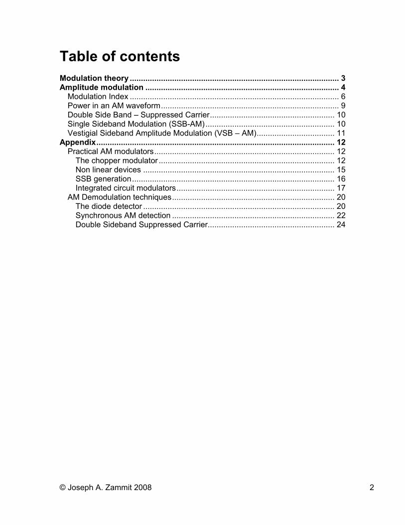
Modulation theory A sine wave is represented as follows
( ) (2 ( ))c cv t ACos f t tπ φ= +
The symbols A, fc and Φ(t) all represent parameters that can be modulated in the carrier waveform in order to carry information. The modulation schemes are known as: A – Amplitude Modulation fc – Frequency Modulation Φ(t) – Phase Modulation Modulation is important since it lets any portion of the radio frequency spectrum used to transmit data. Here we are talking about analog modulation i.e. the transmission of analog signals, mostly audio and video signals. Also the method of transmission will vary according to the portion of the radio frequency spectrum used. The type of modulation used depends on the part of radio frequency spectrum used and the bandwidth needed for the particular application. Analogue modulation continuously varies the carrier with the modulating signal. Digital Modulation switches the carrier on/off with the digital signal applied to the input.
© Joseph A. Zammit 2008 4
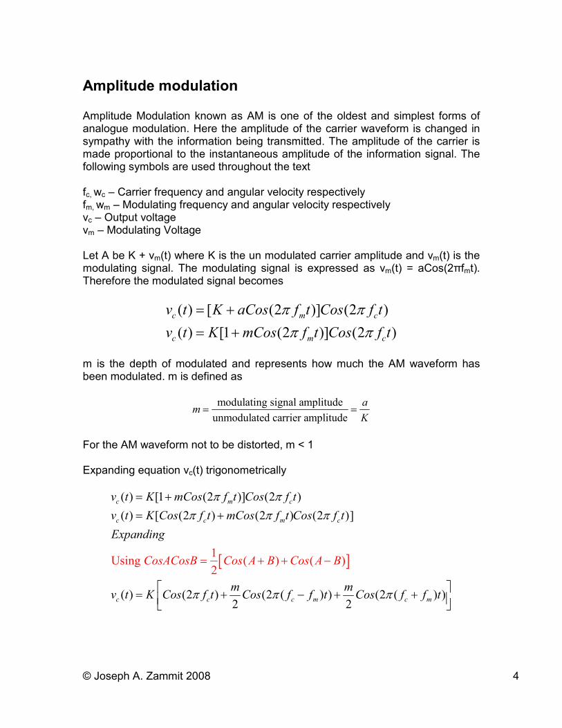
Amplitude modulation Amplitude Modulation known as AM is one of the oldest and simplest forms of analogue modulation. Here the amplitude of the carrier waveform is changed in sympathy with the information being transmitted. The amplitude of the carrier is made proportional to the instantaneous amplitude of the information signal. The following symbols are used throughout the text fc, wc – Carrier frequency and angular velocity respectively fm, wm – Modulating frequency and angular velocity respectively vc – Output voltage vm – Modulating Voltage Let A be K + vm(t) where K is the un modulated carrier amplitude and vm(t) is the modulating signal. The modulating signal is expressed as vm(t) = aCos(2πfmt). Therefore the modulated signal becomes
( ) [ (2 )] (2 )
( ) [1 (2 )] (2 )
c m c
c m c
v t K aCos f t Cos f t
v t K mCos f t Cos f t
π π
π π
= +
= +
m is the depth of modulated and represents how much the AM waveform has been modulated. m is defined as
modulating signal amplitude
unmodulated carrier amplitude
am
K= =
For the AM waveform not to be distorted, m < 1 Expanding equation vc(t) trigonometrically
[ ]1Using
( ) [1 (2 )] (2 )
( ) [ (2 ) (2 ) (2 )]
( ) (2
( ) ( )
) (2 ( ) ) (2 ( ) )2 2
2
c m c
c c m c
c c c m c m
CosA
v t K mCos f t Cos f t
v t K Cos f t mCos f t Cos f t
Expanding
m mv t K Cos f t Cos f f
CosB Cos A B Cos A B
t Cos f f t
π π
π π π
π π π
= +
= +
= + − + +
+ + −
=
© Joseph A. Zammit 2008 5
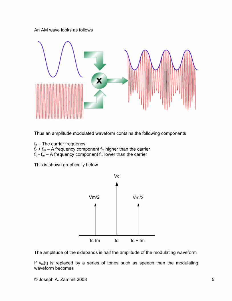
An AM wave looks as follows
Thus an amplitude modulated waveform contains the following components fc – The carrier frequency fc + fm – A frequency component fm higher than the carrier fc - fm – A frequency component fm lower than the carrier This is shown graphically below
fc fc + fmfc-fm
Vc
Vm/2 Vm/2
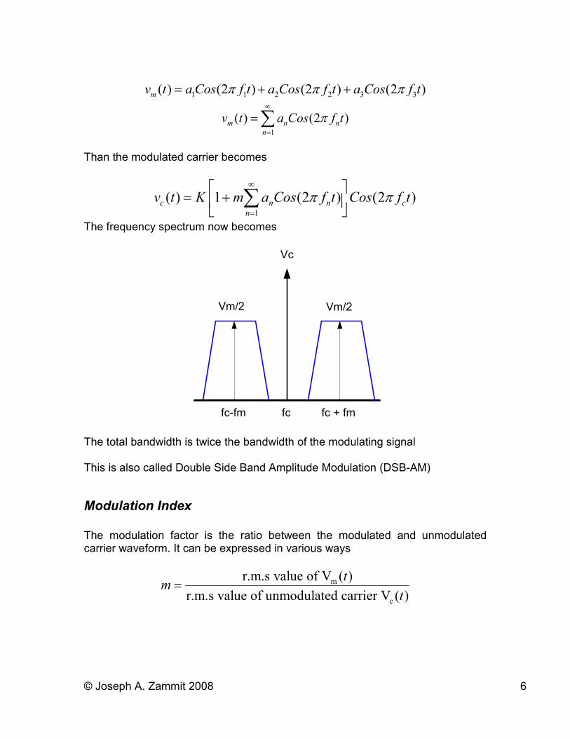
The amplitude of the sidebands is half the amplitude of the modulating waveform If vm(t) is replaced by a series of tones such as speech than the modulating waveform becomes
© Joseph A. Zammit 2008 6
1 1 2 2 3 3( ) (2 ) (2 ) (2 )mv t a Cos f t a Cos f t a Cos f tπ π π= + +
1
( ) (2 )m n n
n
v t a Cos f tπ∞
=
=∑
Than the modulated carrier becomes
1
( ) 1 (2 ) (2 )c n n c
n
v t K m a Cos f t Cos f tπ π∞
=
= +
∑
The frequency spectrum now becomes
fc fc + fmfc-fm
Vc
Vm/2 Vm/2
The total bandwidth is twice the bandwidth of the modulating signal This is also called Double Side Band Amplitude Modulation (DSB-AM)
Modulation Index
The modulation factor is the ratio between the modulated and unmodulated carrier waveform. It can be expressed in various ways
m
c
r.m.s value of V ( )
r.m.s value of unmodulated carrier V ( )
tm
t=
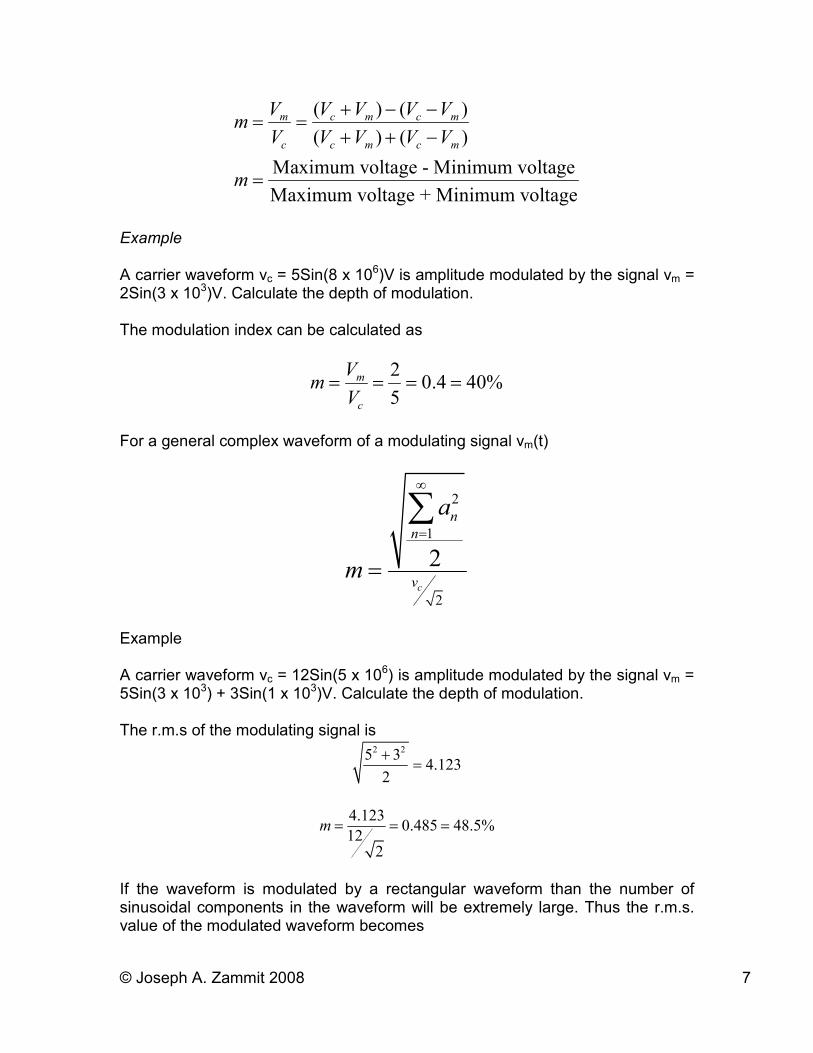
© Joseph A. Zammit 2008 7
( ) ( )
( ) ( )
Maximum voltage - Minimum voltage
Maximum voltage + Minimum voltage
m c m c m
c c m c m
V V V V Vm
V V V V V
m
+ − −= =
+ + −
=
Example A carrier waveform vc = 5Sin(8 x 10
6)V is amplitude modulated by the signal vm = 2Sin(3 x 10³)V. Calculate the depth of modulation. The modulation index can be calculated as
2
0.4 40%5
m
c
Vm
V= = = =
For a general complex waveform of a modulating signal vm(t)
2
1
2
2c
n
n
v
a
m
∞
=
=
∑
Example A carrier waveform vc = 12Sin(5 x 10
6) is amplitude modulated by the signal vm = 5Sin(3 x 10³) + 3Sin(1 x 10³)V. Calculate the depth of modulation. The r.m.s of the modulating signal is
2 25 34.123
2
+=
4.123
0.485 48.5%12
2
m = = =
If the waveform is modulated by a rectangular waveform than the number of sinusoidal components in the waveform will be extremely large. Thus the r.m.s. value of the modulated waveform becomes
© Joseph A. Zammit 2008 8
22
0
11
22
T
c TV mV v dt
T= = +∫
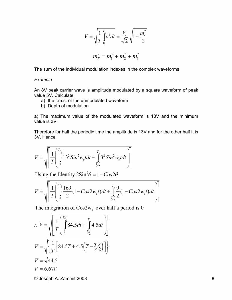
2 2 2 2
1 2 3Tm m m m= + +
The sum of the individual modulation indexes in the complex waveforms Example An 8V peak carrier wave is amplitude modulated by a square waveform of peak value 5V. Calculate
a) the r.m.s. of the unmodulated waveform b) Depth of modulation
a) The maximum value of the modulated waveform is 13V and the minimum value is 3V. Therefore for half the periodic time the amplitude is 13V and for the other half it is 3V. Hence
22 2 2 2
02
2
2
02
c
113 3
Using the Identity 2Sin 1 2
1 169 9(1 2 ) (1 2 )
2 2
The integration of Cos2w over half a period is 0
1
TT
c c
T
TT
c c
T
V Sin w tdt Sin w tdtT
Cos
V Cos w t dt Cos w t dtT
VT
θ θ
= +
= −
= − + −
∴ =
∫ ∫
∫ ∫
( )
2
02
84.5 4.5
184.5 4.5
2
44.5
6.67
TT
T
dt dt
TV T TT
V
V V
+
= + −
=
=
∫ ∫
© Joseph A. Zammit 2008 9
b) To find the modulation index
286.67 1
22
0.884 88.4%
T
T
m
m or
= +
∴ =
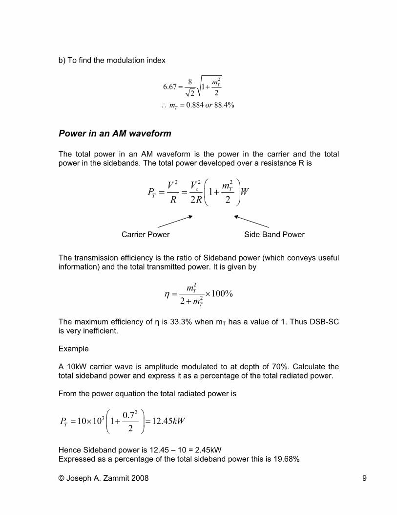
Power in an AM waveform
The total power in an AM waveform is the power in the carrier and the total power in the sidebands. The total power developed over a resistance R is
2 22
12 2
c TT
V mVP W
R R
= = +
The transmission efficiency is the ratio of Sideband power (which conveys useful information) and the total transmitted power. It is given by
2
2100%
2
T
T
m
mη = ×
+
The maximum efficiency of η is 33.3% when mT has a value of 1. Thus DSB-SC is very inefficient. Example A 10kW carrier wave is amplitude modulated to at depth of 70%. Calculate the total sideband power and express it as a percentage of the total radiated power. From the power equation the total radiated power is
23 0.7
10 10 1 12.452
TP kW
= × + =
Hence Sideband power is 12.45 – 10 = 2.45kW Expressed as a percentage of the total sideband power this is 19.68%
Carrier Power Side Band Power
© Joseph A. Zammit 2008 10
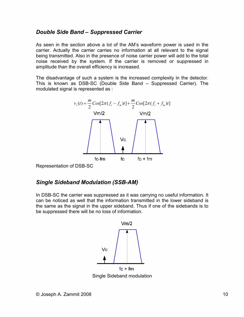
Double Side Band – Suppressed Carrier
As seen in the section above a lot of the AM’s waveform power is used in the carrier. Actually the carrier carries no information at all relevant to the signal being transmitted. Also in the presence of noise carrier power will add to the total noise received by the system. If the carrier is removed or suppressed in amplitude than the overall efficiency is increased. The disadvantage of such a system is the increased complexity in the detector. This is known as DSB-SC (Double Side Band – Suppressed Carrier). The modulated signal is represented as :
( ) [2 ( ) ] [2 ( ) ]2 2
c c m c m
m mv t Cos f f t Cos f f tπ π= − + +
Representation of DSB-SC
Single Sideband Modulation (SSB-AM)
In DSB-SC the carrier was suppressed as it was carrying no useful information. It can be noticed as well that the information transmitted in the lower sideband is the same as the signal in the upper sideband. Thus if one of the sidebands is to be suppressed there will be no loss of information.
Single Sideband modulation
© Joseph A. Zammit 2008 11
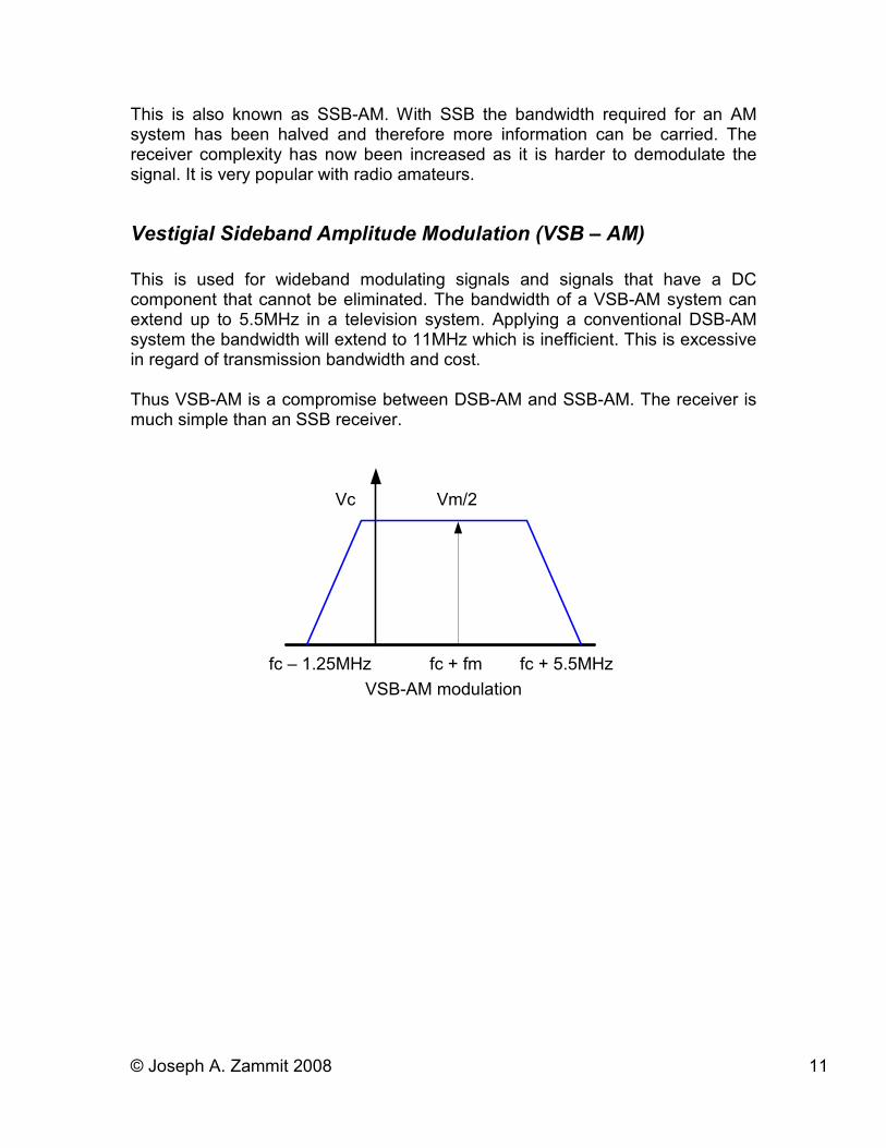
This is also known as SSB-AM. With SSB the bandwidth required for an AM system has been halved and therefore more information can be carried. The receiver complexity has now been increased as it is harder to demodulate the signal. It is very popular with radio amateurs.
Vestigial Sideband Amplitude Modulation (VSB – AM)
This is used for wideband modulating signals and signals that have a DC component that cannot be eliminated. The bandwidth of a VSB-AM system can extend up to 5.5MHz in a television system. Applying a conventional DSB-AM system the bandwidth will extend to 11MHz which is inefficient. This is excessive in regard of transmission bandwidth and cost. Thus VSB-AM is a compromise between DSB-AM and SSB-AM. The receiver is much simple than an SSB receiver.
fc + fm
Vc Vm/2
fc – 1.25MHz fc + 5.5MHz
VSB-AM modulation
© Joseph A. Zammit 2008 12
Appendix
Practical AM modulators
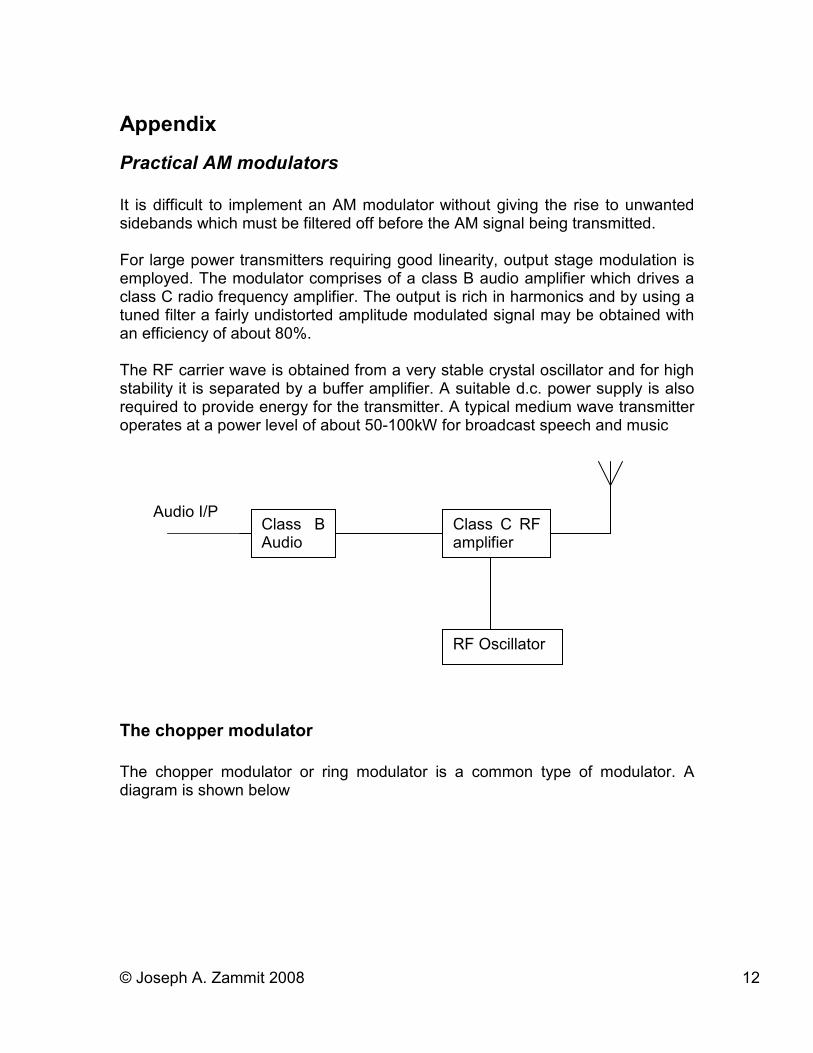
It is difficult to implement an AM modulator without giving the rise to unwanted sidebands which must be filtered off before the AM signal being transmitted. For large power transmitters requiring good linearity, output stage modulation is employed. The modulator comprises of a class B audio amplifier which drives a class C radio frequency amplifier. The output is rich in harmonics and by using a tuned filter a fairly undistorted amplitude modulated signal may be obtained with an efficiency of about 80%. The RF carrier wave is obtained from a very stable crystal oscillator and for high stability it is separated by a buffer amplifier. A suitable d.c. power supply is also required to provide energy for the transmitter. A typical medium wave transmitter operates at a power level of about 50-100kW for broadcast speech and music
The chopper modulator
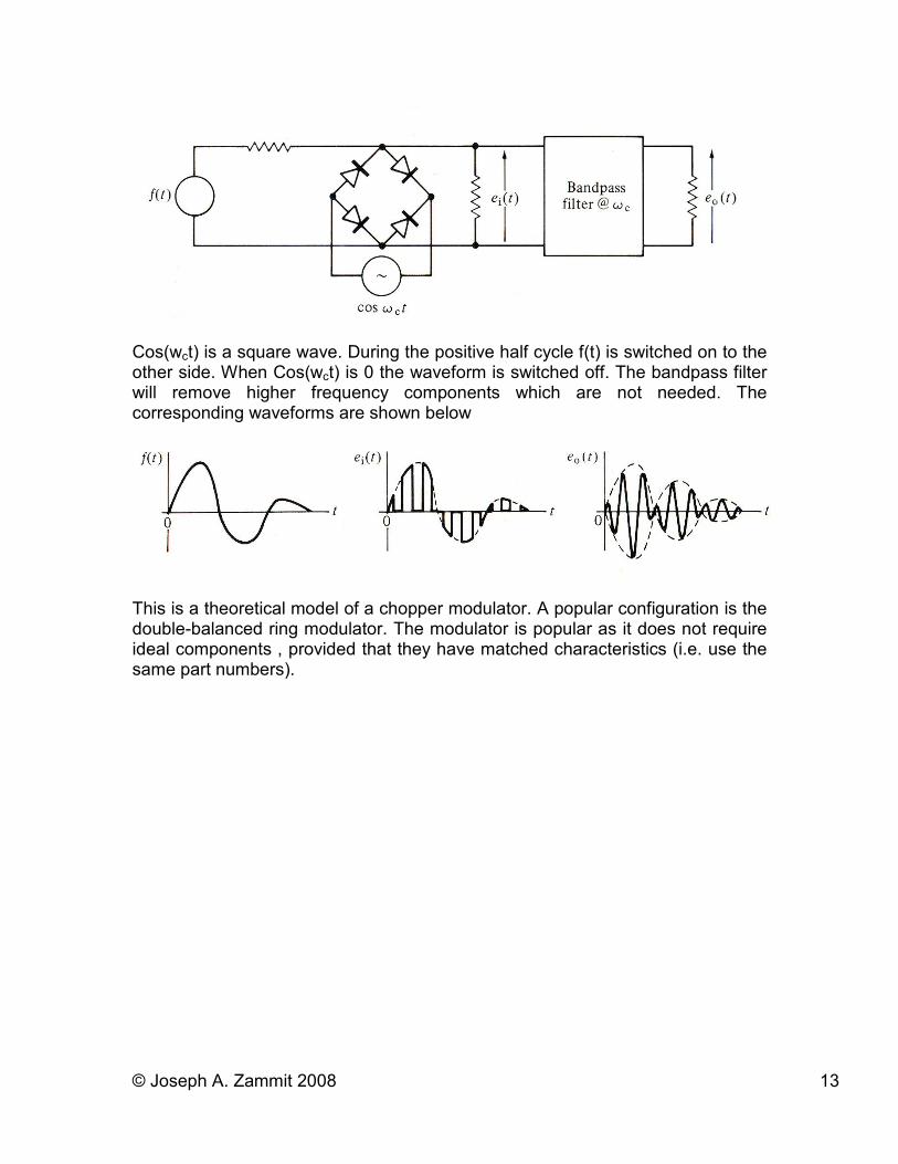
The chopper modulator or ring modulator is a common type of modulator. A diagram is shown below
Class B Audio
Class C RF amplifier
RF Oscillator
Audio I/P
© Joseph A. Zammit 2008 13
Cos(wct) is a square wave. During the positive half cycle f(t) is switched on to the other side. When Cos(wct) is 0 the waveform is switched off. The bandpass filter will remove higher frequency components which are not needed. The corresponding waveforms are shown below
This is a theoretical model of a chopper modulator. A popular configuration is the double-balanced ring modulator. The modulator is popular as it does not require ideal components , provided that they have matched characteristics (i.e. use the same part numbers).
© Joseph A. Zammit 2008 14
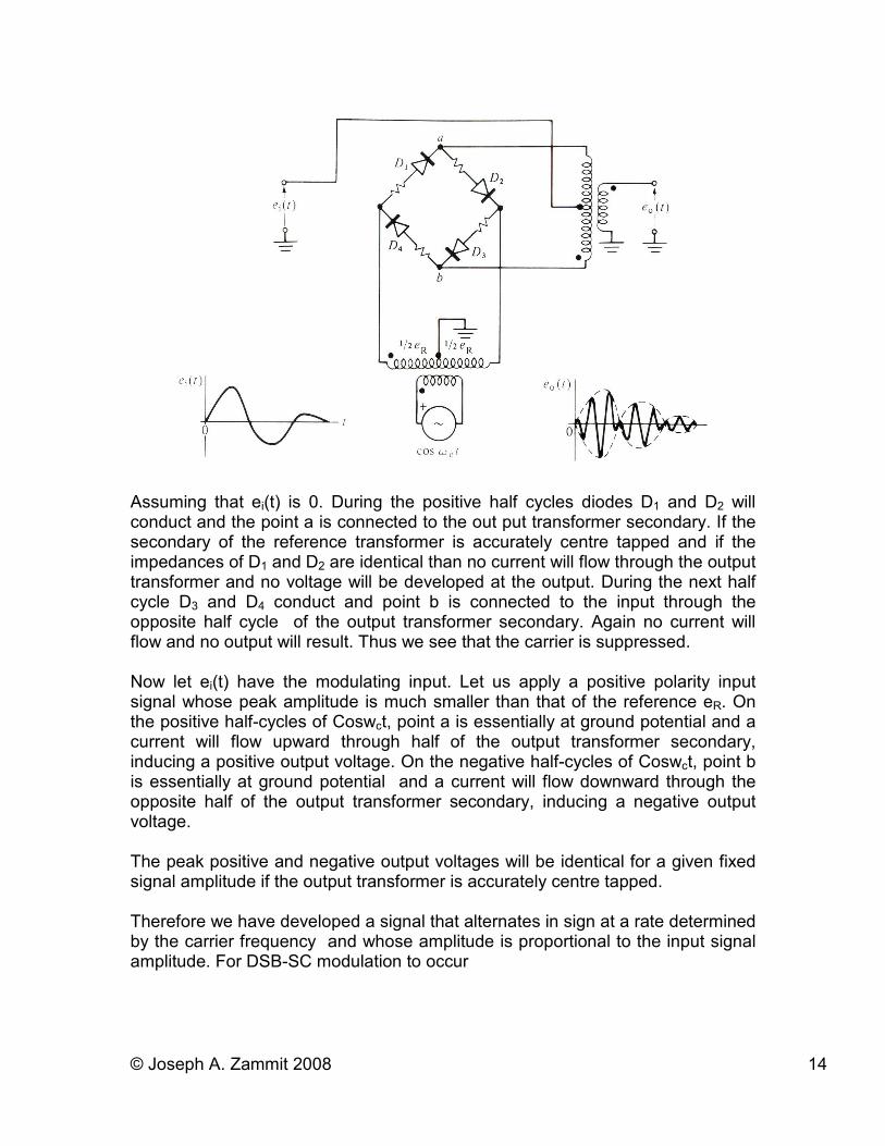
Assuming that ei(t) is 0. During the positive half cycles diodes D1 and D2 will conduct and the point a is connected to the out put transformer secondary. If the secondary of the reference transformer is accurately centre tapped and if the impedances of D1 and D2 are identical than no current will flow through the output transformer and no voltage will be developed at the output. During the next half cycle D3 and D4 conduct and point b is connected to the input through the opposite half cycle of the output transformer secondary. Again no current will flow and no output will result. Thus we see that the carrier is suppressed. Now let ei(t) have the modulating input. Let us apply a positive polarity input signal whose peak amplitude is much smaller than that of the reference eR. On the positive half-cycles of Coswct, point a is essentially at ground potential and a current will flow upward through half of the output transformer secondary, inducing a positive output voltage. On the negative half-cycles of Coswct, point b is essentially at ground potential and a current will flow downward through the opposite half of the output transformer secondary, inducing a negative output voltage. The peak positive and negative output voltages will be identical for a given fixed signal amplitude if the output transformer is accurately centre tapped. Therefore we have developed a signal that alternates in sign at a rate determined by the carrier frequency and whose amplitude is proportional to the input signal amplitude. For DSB-SC modulation to occur
© Joseph A. Zammit 2008 15
[ ]max
1( ) [ ( )]
2i R MAXe t e t<
In practice, an imbalance between diode characteristics and inaccuracies in the transformer centre taps will result in non-ideal performance and carrier leakage. Balancing controls can be added to fully tune out carrier leakage.
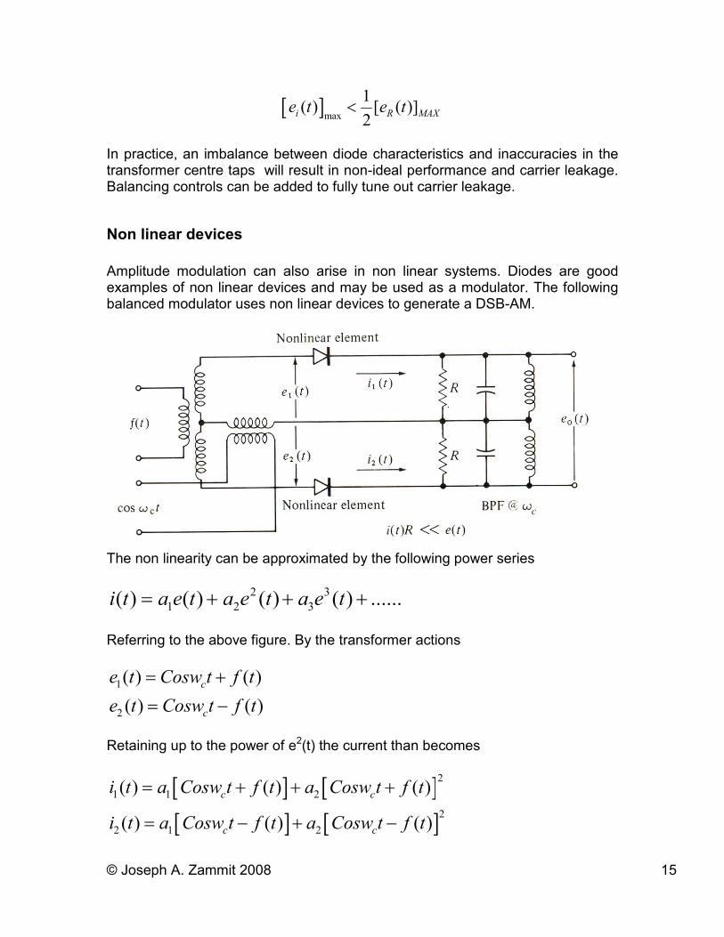
Non linear devices
Amplitude modulation can also arise in non linear systems. Diodes are good examples of non linear devices and may be used as a modulator. The following balanced modulator uses non linear devices to generate a DSB-AM.
The non linearity can be approximated by the following power series
2 3
1 2 3( ) ( ) ( ) ( ) ......i t a e t a e t a e t= + + +
Referring to the above figure. By the transformer actions
1
2
( ) ( )
( ) ( )
c
c
e t Cosw t f t
e t Cosw t f t
= +
= −
Retaining up to the power of e2(t) the current than becomes
[ ] [ ][ ] [ ]
2
1 1 2
2
2 1 2
( ) ( ) ( )
( ) ( ) ( )
c c
c c
i t a Cosw t f t a Cosw t f t
i t a Cosw t f t a Cosw t f t
= + + +
= − + −
© Joseph A. Zammit 2008 16
For a resistive load e0(t) the net voltage is [i1(t) – i2(t)]R the output is
[ ] 12 2
2
( ) ( ) 4 ( ) ( )2
i c
ai t i t R a R f t Cosw t f t
a
− = +
Semiconductor diodes may be used as non linear devices such as modulators. The performance of this type of modulator as for the ring modulator is dependant on how close the characteristics of the diodes can be matched. This is from a class of balanced modulators.
SSB generation
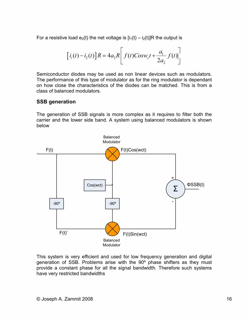
The generation of SSB signals is more complex as it requires to filter both the carrier and the lower side band. A system using balanced modulators is shown below
Cos(wct)
-90º-90º
Σ
F(t)
F(t)’
+
-
F(t)Cos(wct)
F(t)Sin(wct)
Balanced
Modulator
Balanced
Modulator
ΦSSB(t)
This system is very efficient and used for low frequency generation and digital generation of SSB. Problems arise with the 90º phase shifters as they must provide a constant phase for all the signal bandwidth. Therefore such systems have very restricted bandwidths
© Joseph A. Zammit 2008 17
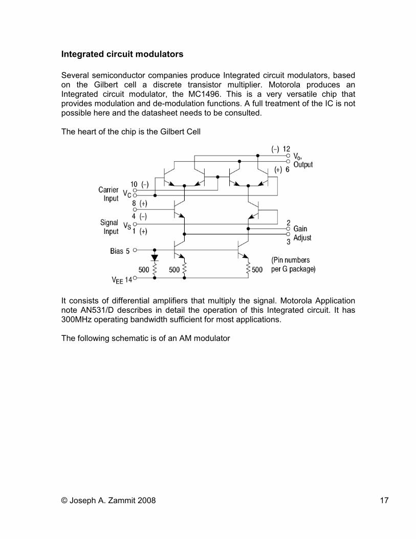
Integrated circuit modulators
Several semiconductor companies produce Integrated circuit modulators, based on the Gilbert cell a discrete transistor multiplier. Motorola produces an Integrated circuit modulator, the MC1496. This is a very versatile chip that provides modulation and de-modulation functions. A full treatment of the IC is not possible here and the datasheet needs to be consulted. The heart of the chip is the Gilbert Cell
It consists of differential amplifiers that multiply the signal. Motorola Application note AN531/D describes in detail the operation of this Integrated circuit. It has 300MHz operating bandwidth sufficient for most applications. The following schematic is of an AM modulator
© Joseph A. Zammit 2008 18
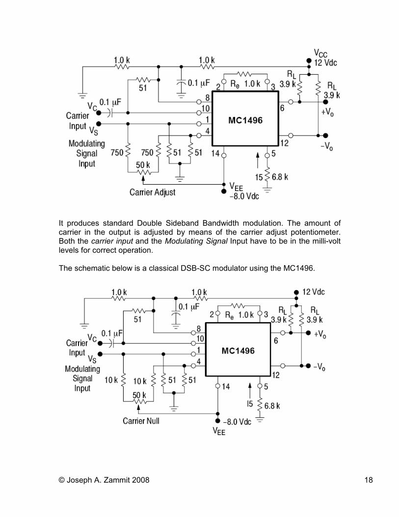
It produces standard Double Sideband Bandwidth modulation. The amount of carrier in the output is adjusted by means of the carrier adjust potentiometer. Both the carrier input and the Modulating Signal Input have to be in the milli-volt levels for correct operation. The schematic below is a classical DSB-SC modulator using the MC1496.
© Joseph A. Zammit 2008 19
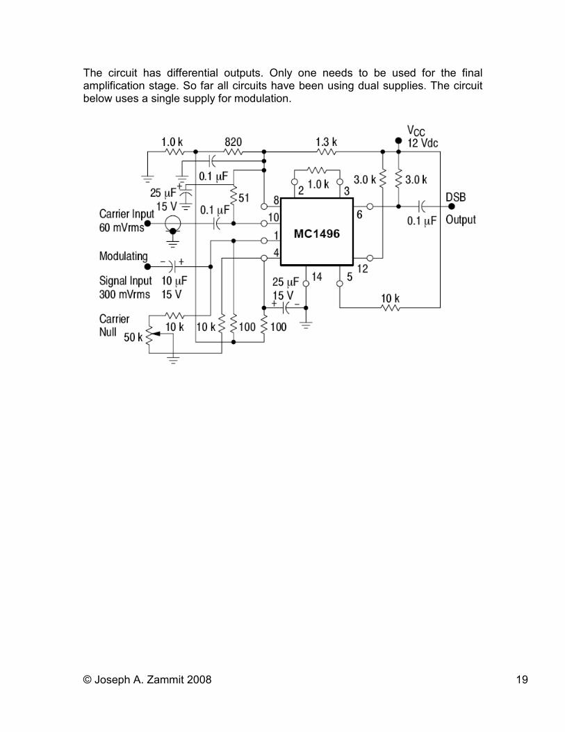
The circuit has differential outputs. Only one needs to be used for the final amplification stage. So far all circuits have been using dual supplies. The circuit below uses a single supply for modulation.
© Joseph A. Zammit 2008 20
AM Demodulation techniques
Detection or demodulation is the process of recovering the intelligent signals from an amplitude-modulated wave. Most radio receivers employ a diode detector and most SSB systems use one type or other of balanced modulator.
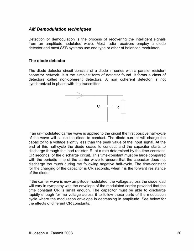
The diode detector
The diode detector circuit consists of a diode in series with a parallel resistor-capacitor network. It is the simplest form of detector found. It forms a class of detectors called non-coherent detectors. A non coherent detector is not synchronized in phase with the transmitter
If an un-modulated carrier wave is applied to the circuit the first positive half-cycle of the wave will cause the diode to conduct. The diode current will charge the capacitor to a voltage slightly less than the peak value of the input signal. At the end of this half-cycle the diode cease to conduct and the capacitor starts to discharge through the load resistor, R, at a rate determined by the time-constant, CR seconds, of the discharge circuit. This time-constant must be large compared with the periodic time of the carrier wave to ensure that the capacitor does not discharge too much during me following negative half-cycle. The time-constant for the charging of the capacitor is CR seconds, when r is the forward resistance of the diode. If the carrier wave is now amplitude modulated, the voltage across the diode load will vary in sympathy with the envelope of the modulated carrier provided that the time constant CR is small enough. The capacitor must be able to discharge rapidly enough for me voltage across it to follow those parts of the modulation cycle where the modulation envelope is decreasing in amplitude. See below for the effects of different CR constants.
© Joseph A. Zammit 2008 21
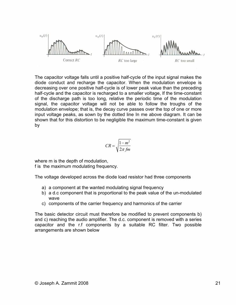
The capacitor voltage falls until a positive half-cycle of the input signal makes the diode conduct and recharge the capacitor. When the modulation envelope is decreasing over one positive half-cycle is of lower peak value than the preceding half-cycle and the capacitor is recharged to a smaller voltage, If the time-constant of the discharge path is too long, relative the periodic time of the modulation signal, the capacitor voltage will not be able to follow the troughs of the modulation envelope; that is, the decay curve passes over the top of one or more input voltage peaks, as sown by the dotted line In me above diagram. It can be shown that for this distortion to be negligible the maximum time-constant is given by
21
2
mCR
fmπ−
=
where m is the depth of modulation, f is the maximum modulating frequency. The voltage developed across the diode load resistor had three components
a) a component at the wanted modulating signal frequency b) a d.c component that is proportional to the peak value of the un-modulated
wave c) components of the carrier frequency and harmonics of the carrier
The basic detector circuit must therefore be modified to prevent components b) and c) reaching the audio amplifier. The d.c. component is removed with a series capacitor and the r.f components by a suitable RC filter. Two possible arrangements are shown below
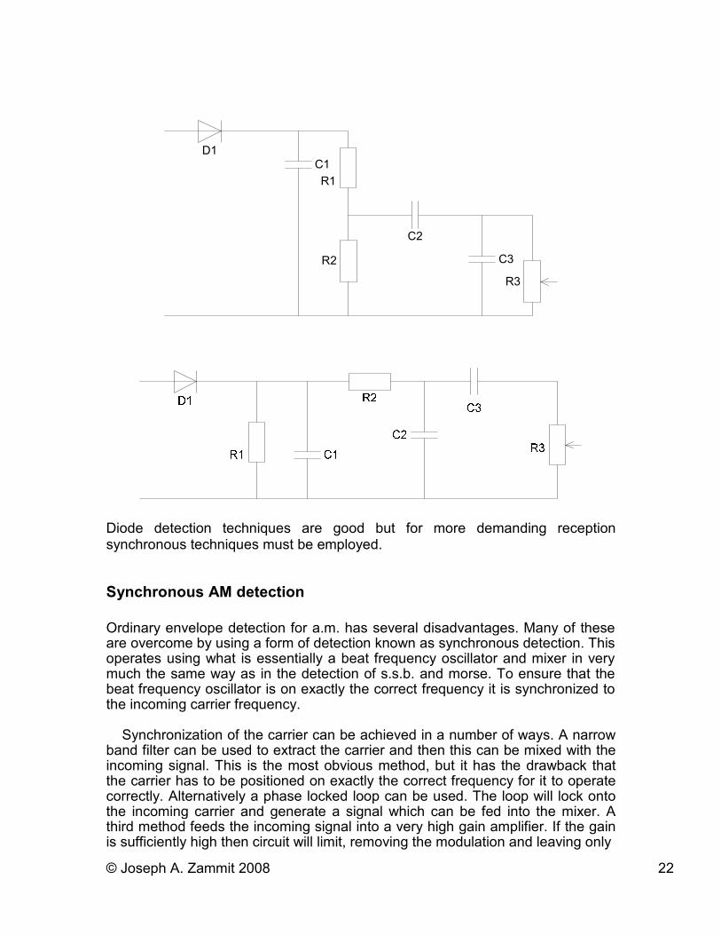
© Joseph A. Zammit 2008 22
D1C1
R1
R2
C2
C3
R3
Diode detection techniques are good but for more demanding reception synchronous techniques must be employed.
Synchronous AM detection
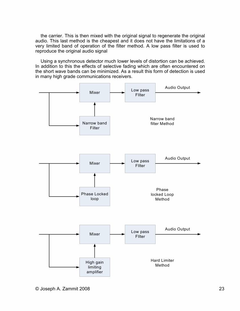
Ordinary envelope detection for a.m. has several disadvantages. Many of these are overcome by using a form of detection known as synchronous detection. This operates using what is essentially a beat frequency oscillator and mixer in very much the same way as in the detection of s.s.b. and morse. To ensure that the beat frequency oscillator is on exactly the correct frequency it is synchronized to the incoming carrier frequency.
Synchronization of the carrier can be achieved in a number of ways. A narrow
band filter can be used to extract the carrier and then this can be mixed with the incoming signal. This is the most obvious method, but it has the drawback that the carrier has to be positioned on exactly the correct frequency for it to operate correctly. Alternatively a phase locked loop can be used. The loop will lock onto the incoming carrier and generate a signal which can be fed into the mixer. A third method feeds the incoming signal into a very high gain amplifier. If the gain is sufficiently high then circuit will limit, removing the modulation and leaving only
© Joseph A. Zammit 2008 23
the carrier. This is then mixed with the original signal to regenerate the original
audio. This last method is the cheapest and it does not have the limitations of a very limited band of operation of the filter method. A low pass filter is used to reproduce the original audio signal
Using a synchronous detector much lower levels of distortion can be achieved.
In addition to this the effects of selective fading which are often encountered on the short wave bands can be minimized. As a result this form of detection is used in many high grade communications receivers.
MixerLow pass
FIlter
Narrow band
Filter
Audio Output
Narrow band
filter Method
MixerLow pass
FIlter
Phase Locked
loop
Audio Output
Phase
locked Loop
Method
MixerLow pass
FIlter
High gain
limiting
amplifier
Audio Output
Hard Limiter
Method
© Joseph A. Zammit 2008 24
Double Sideband Suppressed Carrier
Although Double Sideband Suppressed Carrier (DSB-SC.) is very seldom used, it is included here for the sake of completeness. Occasionally it is used by radio amateurs because it is simpler and cheaper to make a DSB-SC. transmitter than a full SSB. one, because it does not need the expensive filtering required by SSB. To demodulate DSB-SC. the most convenient method is simply to use the filter
in the receiver to remove one of the sidebands. Then it can be demodulated as if it were SSB. in the normal way. To demodulate DSB-SC, making full use of both of the sidebands requires
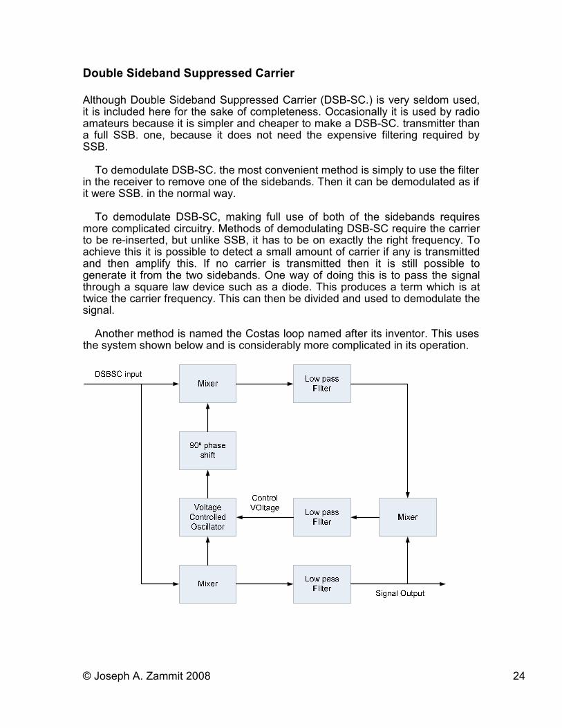
more complicated circuitry. Methods of demodulating DSB-SC require the carrier to be re-inserted, but unlike SSB, it has to be on exactly the right frequency. To achieve this it is possible to detect a small amount of carrier if any is transmitted and then amplify this. If no carrier is transmitted then it is still possible to generate it from the two sidebands. One way of doing this is to pass the signal through a square law device such as a diode. This produces a term which is at twice the carrier frequency. This can then be divided and used to demodulate the signal. Another method is named the Costas loop named after its inventor. This uses
the system shown below and is considerably more complicated in its operation.