
AMD Bolton Fusion Controller Hub Register Programming ... · ... IN THE MPEG PATENT PORTFOLIO,...
100
AMD Bolton FCH Register Programming Requirements 51191 Publication # Rev 3.00 Revision: August 2014 Issue Date:
Transcript of AMD Bolton Fusion Controller Hub Register Programming ... · ... IN THE MPEG PATENT PORTFOLIO,...

© 201
AMD Bolton FCHRegister Programming Requirements
51191Publication # Rev 3.00Revision:August 2014Issue Date:
4 Advanced Micro Devices, Inc. 51191 AMD Bolton Register Programming Requirements Rev 3.00 Page 1

51191 AMD Bolton Register Programming Requirements Rev 3.00 © 2014 Advanced Micro Devices, Inc.Page 2
© 2014 Advanced Micro Devices, Inc. All rights reserved.
The information contained herein is for informational purposes only, and is subject to change without notice. While every precaution has been taken in the preparation of this document, it may contain technical inaccuracies, omissions and typographical errors, and AMD is under no obligation to update or otherwise correct this information. Advanced Micro Devices, Inc. makes no representations or warranties with respect to the accuracy or completeness of the contents of this document, and assumes no liability of any kind, including the implied warranties of noninfringement, merchantability or fitness for particular purposes, with respect to the operation or use of AMD hardware, software or other products described herein. No license, including implied or arising by estoppel, to any intellectual property rights is granted by this document. Terms and limitations applicable to the purchase or use of AMD’s products are as set forth in a signed agreement between the parties or in AMD's Standard Terms and Conditions of Sale.
TrademarksAMD, the AMD Arrow logo, and combinations thereof are trademarks of Advanced Micro Devices, Inc. Other product names used in this publication are for identification purposes only and may be trademarks of their respective companies.
HyperTransport is a licensed trademark of the HyperTransport Technology Consortium.
PCI Express and PCIe are registered trademarks of PCI-Special Interest Group (PCI-SIG).
HDMI is a trademark of HDMI Licensing, LLC.
Microsoft and Windows are registered trademarks of Microsoft Corporation.
Dolby Laboratories, Inc.Manufactured under license from Dolby Laboratories.
Rovi CorporationThis device is protected by U.S. patents and other intellectual property rights. The use of Rovi Corporation's copy protection technology in the device must be authorized by Rovi Corporation and is intended for home and other limited pay-per-view uses only, unless otherwise authorized in writing by Rovi Corporation.
Reverse engineering or disassembly is prohibited.
USE OF THIS PRODUCT IN ANY MANNER THAT COMPLIES WITH THE MPEG ACTUAL OR DE FACTO VIDEO AND/OR AUDIO STANDARDS IS EXPRESSLY PROHIBITED WITHOUT ALL NECESSARY LICENSES UNDER APPLICABLE PATENTS. SUCH LICENSES MAY BE ACQUIRED FROM VARIOUS THIRD PARTIES INCLUDING, BUT NOT LIMITED TO, IN THE MPEG PATENT PORTFOLIO, WHICH LICENSE IS AVAILABLE FROM MPEG LA, L.L.C., 6312 S. FIDDLERS GREEN CIRCLE, SUITE 400E, GREENWOOD VILLAGE, COLORADO 80111.
© 2014 Advanced Micro Devices, Inc. 51191 AMD Bolton Register Programming Requirements Rev 3.00 Page 3
Revision History
Date Revision Description
August 2014 3.00 Initial public release.
© 2014 Advanced Micro Devices, Inc. 51191 AMD Bolton Register Programming Requirements Rev 3.00 Page 3

51191 AMD Bolton Register Programming Requirements Rev 3.00 © 2014 Advanced Micro Devices, Inc.Page 4

Table of Contents
Revision History . . . . . . . . . . . . . . . . . . . . . . . . . . . . . . . . . . . . . . . . . . . . . . . . . . . . . . . . . . . . . . . . . . ...3
1 Introduction .........................................................................................................................................131.1 About This Manual ................................................................................................................... 131.2 AMD Bolton Block Diagram .................................................................................................... 141.3 How to Read the Information in this Document ....................................................................... 15
2 ACPI/SMBUS Controller (bus-0, dev-20, fun-0) ...............................................................................162.1 Revision ID 162.2 ACPI Memory Mapped I/O Enable .......................................................................................... 162.3 MMIO Programming for Legacy Devices ................................................................................ 162.4 Enable Boot Timer ................................................................................................................... 172.5 RTC Wake Up .......................................................................................................................... 172.6 Keyboard Reset Settings for Legacy Free Systems .................................................................. 182.7 NB Power Good Control on System Reset ............................................................................... 182.8 Enhancement of FanOut0 Control ........................................................................................... 182.9 Extend SerIrq Request .............................................................................................................. 192.10 Mt C1e Enable ......................................................................................................................... 192.11 HWM Sensor CLK ................................................................................................................... 192.12 Clear Status of SATA PERR ................................................................................................... 202.13 Enable Delayed SLP_S3/S5 to Motherboard ........................................................................... 202.14 Enable C-State Wake-up before Warm Reset .......................................................................... 202.15 Enable DMAACTIVE# ........................................................................................................... 202.16 IMC Enable .............................................................................................................................. 212.17 Adjust PM Timer Read Mechanism ......................................................................................... 212.18 PCIe® Wake Status and PME Wake Status ............................................................................. 212.19 Set RTC OSC Output Drive ..................................................................................................... 21
3 LPC Controller (bus-0, dev-20, fun-3) ................................................................................................233.1 SPI Controller MMIO Base Address ....................................................................................... 233.2 Enable SPI ROM Prefetch ........................................................................................................ 233.3 Enable LPC DMA Function ..................................................................................................... 233.4 Enable ClkRun Function ........................................................................................................... 243.5 Enable LPCCLK0 Power-Down Function .............................................................................. 243.6 Disable LPC A-Link Cycle Bypass .......................................................................................... 243.7 LPC Cycle Abort Sync Threshold Setting ................................................................................ 24
4 UMI and A/B-Link Settings - Indirect I/O Access .............................................................................254.1 Defining AB_REG_BAR ........................................................................................................ 254.2 Upstream DMA Access ........................................................................................................... 254.3 PCIB Prefetch Settings ............................................................................................................ 254.4 OHCI Prefetch Settings ............................................................................................................ 264.5 B-Link Client’s Credit Variable Settings for the Downstream Arbitration Equation ............. 264.6 Setting B-Link Prefetch Mode .................................................................................................. 264.7 Detection of Upstream Interrupts ............................................................................................ 26
© 2014 Advanced Micro Devices, Inc. 51191 AMD Bolton Register Programming Requirements Rev 3.00 Page 7

4.8 Downstream Posted Transactions to Pass Non-Posted Transactions ........................................274.9 AB and UMI/GPP Clock Gating ...............................................................................................274.10 AB Int_Arbiter Enhancement ...................................................................................................274.11 Requester ID ..............................................................................................................................274.12 UMI LOs/L1 NAK Reduction ...................................................................................................284.13 Power Saving Feature for UMI Lanes ...................................................................................... 284.14 Non-Posted Memory Write Support 284.15 SMI Ordering ............................................................................................................................294.16 Posted Pass Non-Posted Feature ................................................................................................294.17 UMI Speed Change ...................................................................................................................294.18 UMI L1 Configuration ...............................................................................................................30
5 PCIe® General Purpose Ports .............................................................................................................315.1 GPP Lane Configuration ...........................................................................................................315.2 GPP Port 0/1/2/3 .......................................................................................................................315.3 GPP Reset ..................................................................................................................................325.4 PCIe® Ports De-emphasis Settings ..........................................................................................335.5 Write Capability for PCIe® Read-Only Registers ....................................................................335.6 Serial Number Capability ........................................................................................................345.7 Multi-function Enable ...............................................................................................................345.8 GPP Upstream Memory Write Arbitration Enhancement ........................................................345.9 GPP Memory Write Max Payload Improvement .....................................................................345.10 Multiple GPP Device Support ...................................................................................................355.11 Separate Control for Release from Reset and Hold Training for each GPP Port ......................355.12 GPP PCIe® Native Interrupt Support ........................................................................................355.13 GPP Error Reporting Configuration .........................................................................................365.14 Hot Plug: PCIe® Native Support .............................................................................................365.15 Link Bandwidth Notification Capability Enable ......................................................................365.16 Power Saving Feature for GPP Lanes ......................................................................................375.17 GPP L1 PM Request NAK Reduction .......................................................................................375.18 GPP ASPM L1/L0s Enable ......................................................................................................385.19 GPP Immediate Ack PM_Active_State_Request_L1 ...............................................................385.20 GPP Dynamic Power Saving ....................................................................................................39
5.20.1 GPP Power Saving with Hot Plug/Unplug ......................................................................405.20.2 GPP Power Saving – RX/TX Pads Power Up/Down Mapping Table ..............................41
5.21 GPP Gen2 Speed Change ..........................................................................................................42
6 PCIB (PCI-bridge, bus-0, dev-20, fun-04) ..........................................................................................436.1 PCI-bridge Subtractive Decode ................................................................................................436.2 PCI-bridge Upstream Dual Address Window ..........................................................................436.3 One-Channel Mode ....................................................................................................................436.4 CLKRUN# ................................................................................................................................446.5 PCI Bus GNT3# .........................................................................................................................44
7 USB Controllers ..................................................................................................................................457.1 Device Mapping of OHCI, EHCI, and XHCI Controllers ........................................................45
7.1.1 Device List for Bolton ......................................................................................................45
51191 AMD Bolton Register Programming Requirements Rev 3.00 © 2014 Advanced Micro Devices, Inc.Page 8

7.2 Enabling USB Controllers ........................................................................................................ 467.3 USB S4/S5 Wake-up or PHY Power-down Support ............................................................... 467.4 USB PHY Auto-Calibration Setting ......................................................................................... 477.5 USB Reset Sequence ................................................................................................................ 477.6 USB Advanced Sleep Control .................................................................................................. 477.7 USB Delay UMI L1 State ......................................................................................................... 487.8 USB 2.0 Ports Driving Strength ............................................................................................... 487.9 EHCI In and Out Data Packet FIFO Threshold ........................................................................ 507.10 OHCI MSI Function ................................................................................................................. 507.11 EHCI MSI Function .................................................................................................................. 507.12 USB SMI Handshake ................................................................................................................ 517.13 EHCI Async Park Control ........................................................................................................ 517.14 Extend InterPacket Gap ............................................................................................................ 517.15 Empty List Mode ...................................................................................................................... 527.16 L1 Early Exit ............................................................................................................................. 527.17 EHCI PING Response Fix Enable ............................................................................................ 527.18 EHCI Async Stop Enhancement .............................................................................................. 537.19 Synchronize OHCI SOF ........................................................................................................... 537.20 OHCI Periodic List Advance .................................................................................................... 537.21 OHCI Arbiter Mode ................................................................................................................. 547.22 USB 2.0 Global Clock Gating .................................................................................................. 547.23 USB 1.1 Full-Speed False CRC Errors Detected - CDR Logic Enhancement ......................... 557.24 Allow LS Devices to Wake up System from Sx states when EHCI Owns the Port ................. 557.25 Fix for Long Read Latency Delays during Frame List Read by EHCI Controller Causing
Malfunction ............................................................................................................................... 557.26 Fix for EHCI's BLM Data Cache Issue .................................................................................... 567.27 Fix for OHCI Arbiter Issue ....................................................................................................... 567.28 Enhancement for USB Device Detection ................................................................................. 567.29 Frame Babble Enhancement ..................................................................................................... 577.30 EHCI Controller Data Babble to CRC Conversion Feature Disable ........................................ 577.31 EHCI Controller Micro-Frame Counter Sync Enhancement .................................................... 577.32 OHCI Packet Buffer Threshold Settings .................................................................................. 587.33 EHCI Frame List Processing Enhancement ............................................................................. 587.34 Speed Field Enhancement ......................................................................................................... 587.35 Save Status of EHCI/OHCI Connect/Disconnect in S3 ........................................................... 597.36 ISO Device CRC False Error Detection .................................................................................. 597.37 EHCI Data Cache Enhancement ............................................................................................... 597.38 Unexpected Linux Driver TD Setup Causing EHCI to Hang ................................................... 607.39 Reset Connect Timer when Disconnecting ............................................................................... 607.40 EHCI_PME Should Be Gated by PME Enable Bit .................................................................. 607.41 EHCI Required to Support De-Linking Async Active QH ...................................................... 607.42 Enhance EHCI QTD with SOF ................................................................................................. 617.43 Enable Cycle-based ECHI PIE Handshake Ready ................................................................... 617.44 Enhance EHCI/OHCI Resume/Disconnect Detection Timer ................................................... 617.45 Enhance EHCI/OHCI Hold Resume ........................................................................................ 61
8 USB xHCI Controllers .......................................................................................................................63
© 2014 Advanced Micro Devices, Inc. 51191 AMD Bolton Register Programming Requirements Rev 3.00 Page 9

8.1 SMI Enable ................................................................................................................................638.2 BLM Message Enable ...............................................................................................................638.3 USB 3.0 (SuperSpeed) PHY Configuration ..............................................................................638.4 USB 3.0 Reference Clock ..........................................................................................................638.5 USB 3.0 Global Clock Gating ...................................................................................................648.6 xHCI Controller PCI Configuration Space "Read Only" Registers Write Lock Enable ...........648.7 xHCI USB 2.0 PHY Settings .....................................................................................................648.8 Allow Access to EHCI/OHCI Register through JTAG .............................................................668.9 USB PHY Suspend State Enhancement ....................................................................................668.10 UMI Lane Configuration Information for xHCI Firmware to Calculate the Bandwidth for
USB 3.0 ISOC Devices ............................................................................................................668.11 Fix for Incorrect Gated Signals in xhc_to_s5 ............................................................................668.12 xHCI USB 2.0 PHY Clock Gating and Rise Time Configuration ........................................... 678.13 xHCI Clear Pending PME on Sx Entry ....................................................................................678.14 D3Cold ccu Sequencing Enhancement ......................................................................................688.15 Set HCI Version to 1.0 ..............................................................................................................698.16 xHCI 1.0 Sub-Features Supported .............................................................................................698.17 xHCI USB 2.0 Loopback RX SE0 ............................................................................................708.18 xHC S0 BLM Reset Mode .........................................................................................................708.19 Enhance xHC Ent_Flag .............................................................................................................708.20 Enhance TRB Pointer when both MSE and SKIP TRB IOC EVT Open ..................................708.21 LPM Broadcast Disable .............................................................................................................708.22 Enhance xHC FS/LS Connect ...................................................................................................718.23 Enhance xHC ISOCH td_cmp ...................................................................................................718.24 LPM Clock 5us Select ...............................................................................................................718.25 Enhance DPP ERR as XactErr ..................................................................................................718.26 Enhance U2IF PME Enable .......................................................................................................728.27 Enhance U2IF S3 Disconnect Detection ...................................................................................728.28 Stream Error Handling ...............................................................................................................728.29 FLA Deassert .............................................................................................................................728.30 LPM Ctrl Improvement .............................................................................................................728.31 Enhance Resume after Disconnect ............................................................................................738.32 Enhance SS HD Detected on Plug-in during S3 ........................................................................738.33 Frame Babble Reporting ............................................................................................................738.34 DCP Halt RSTSM OFF .............................................................................................................738.35 Enable DCP DPH Check ...........................................................................................................748.36 DCP LTSSM Inactive to Rxdetect ............................................................................................748.37 Enhance DCP EP State ..............................................................................................................748.38 DCP Remote Wakeup Capable ..................................................................................................748.39 Enhance SS HS Detection during S3 .........................................................................................748.40 Enhance U1 Timer .....................................................................................................................758.41 Enhance LPM U2Entry State ....................................................................................................758.42 Enhance SSIF PME ...................................................................................................................758.43 Enable ERDY Send when DBC Detects HIT/HOT ..................................................................758.44 Block HIT/HOT until Service Interval is Done .........................................................................768.45 Enhance LPM Host Initial L1 Exit ............................................................................................768.46 xHCI ISO Device CRC False Error Detection .........................................................................76
51191 AMD Bolton Register Programming Requirements Rev 3.00 © 2014 Advanced Micro Devices, Inc.Page 10

8.47 Enable FW Enhancement on XHC Clock Control when Memory Power Saving is Disabled . 778.48 U2IF Remote Wake Select ....................................................................................................... 778.49 HS Data Toggle Error Handling ............................................................................................... 778.50 L1 Residency Duration ............................................................................................................. 778.51 CCU Mode................................................................................................................................ 78
9 SATA (bus-0, dev-17, fun-0) ..............................................................................................................799.1 SATA Configuration ................................................................................................................ 799.2 Optionally Disable Unused SATA Ports ................................................................................. 799.3 Staggered SATA PHY DLL Reset .......................................................................................... 809.4 SATA Subclass Programming Sequence ................................................................................. 809.5 SATA PHY Programming Sequence ....................................................................................... 819.6 SATA Identification Programming Sequence for IDE Mode ................................................. 829.7 External SATA Ports Indication Registers .............................................................................. 849.8 Optionally Disable Aggressive Link Power Management ...................................................... 859.9 Optionally Disable Port Multiplier and FIS-based Switching Support ................................... 859.10 Disable CCC (Command Completion Coalescing) Support ................................................... 869.11 CCC Interrupt Configuration ................................................................................................... 869.12 Optionally Disable SATA MSI Capability, Programming of MSI Related Registers, and
Disable D3 Power State ........................................................................................................... 869.12.1 SATA MSI Settings ..........................................................................................................869.12.2 D3 Power State Settings ...................................................................................................879.12.3 Capability Pointer Settings ...............................................................................................87
9.13 Disable SATA FLR Capability ................................................................................................ 879.14 SATA PCI Watchdog Timer ................................................................................................... 889.15 SATA/IDE2 Controller Mode and Port Allocation ................................................................. 889.16 Optionally Disable SATA PHY PLL Dynamic Shutdown ...................................................... 899.17 SATA PHY Reference Clock Selections ................................................................................. 909.18 Optionally Enable/Disable Unused IDE Channel .................................................................... 919.19 Enable Hot-removal Detection Enhancement ......................................................................... 919.20 Enable E-SATA Power Saving Enhancement .......................................................................... 919.21 Design Enhancement ................................................................................................................ 929.22 Optionally Enable Support for RAS ........................................................................................ 929.23 Disable Performance Enhancement for Non NCQ ................................................................... 939.24 Identifying Bolton Variants ...................................................................................................... 93
10 SATA IDE Controller 2 (bus-0, dev-20, fun-01) ................................................................................9410.1 Optionally Disable SATA IDE Controller 2 ........................................................................... 9410.2 Hide MSI Capability ................................................................................................................ 9410.3 Optionally Disable Unused IDE Channel ................................................................................ 94
11 HD Audio (bus-0, dev-20, fun-02) ......................................................................................................9511.1 Enabling/Disabling HD Audio Controller ................................................................................ 9511.2 HD Audio I/O Configuration .................................................................................................... 9511.3 HD Audio MSI Capability ....................................................................................................... 95
12 On-Chip Clock Generator ...................................................................................................................96
© 2014 Advanced Micro Devices, Inc. 51191 AMD Bolton Register Programming Requirements Rev 3.00 Page 11
12.1 Internal Clock Generator Enable Status ...................................................................................9612.2 PLL 100Mhz Reference Clock Buffer Setting for Internal Clock Generator Mode ...............9612.3 OSC Clock Setting ...................................................................................................................9612.4 CG_PLL CMOS Clock Driver Setting for Power Saving ........................................................9712.5 Global A-Link/B-Link Clock Gating .......................................................................................9712.6 SSC Setting ...............................................................................................................................9812.7 A-Link/B-Link Clock Low Speed Mode ..................................................................................9812.8 Internal Clock Generator Spread Profile ...................................................................................9812.9 Enable GPP_CLK_REQ# for Power Saving in Internal Clock Mode ...................................100
13 SD Host Controller ...........................................................................................................................10113.1 SD Hold Time Enhancement ...................................................................................................10113.2 SD Base Clock Frequency ......................................................................................................10113.3 SD Disable MSI .......................................................................................................................101
51191 AMD Bolton Register Programming Requirements Rev 3.00 © 2014 Advanced Micro Devices, Inc.Page 12

1 Introduction
1.1 About This Manual
This document lists the register settings required for the proper operation of the AMD Bolton FCH (fusion controller hub).
Most of the register settings described in this document are mandatory and should be implemented as described. The document will be updated periodically with new or revised settings that are determined during the qualification of the Bolton FCH. Please refer to the latest updated document on the AMD NDA site.
This document should be used in conjunction with the related AMD Bolton FCH BIOS Developer's Guide and the AMD Bolton Register Reference Guide.
Note: In this document, changes/additions from the previous release are highlighted in red. Refer to Revision History at the beginning of this document for change details.
© 2014 Advanced Micro Devices, Inc. 51191 AMD Bolton Register Programming Requirements Rev 3.00 Page 13

Introduction
1.2 AMD Bolton Block Diagram
Figure 1 below shows the Bolton internal PCI devices and major functional blocks. Support of features may differ depending on the Bolton variants (Bolton-D2, D3, D4, M3, and E4). Please refer to respective databooks for details.
Figure 1. Bolton Block Diagram
51191 AMD Bolton Register Programming Requirements Rev 3.00 © 2014 Advanced Micro Devices, Inc.Page 14

Introduction
1.3 How to Read the Information in this Document
Tables within this document contain information showing the applicable revision(s), recommended settings, and comments associated with the register. Consider the following example:
• ASIC Rev --> Currently only Rev A0 exists. Newer revisions will be added as they appear in future.
• Register Settings --> Recommended register settings with the register address and controlling bits.For more detailed information about the registers found within this document, refer to the AMD Bolton Register Ref-erence Guide. The applicable section in the Register Reference Guide where the information can be found is marked with "X" in the tables in this document.
ASIC Rev Register Settings Function/CommentBolton All Revs PM_IO 0x52 [5:0] = 0x08 Recommended delay for S3/S4/S5 resume sequence
SATA USB SMBUS PATA HD AUDIO LPC PCI For register details refer to the sections check-marked in Bolton Register Reference Guide
RTC ACPI PM_REG UMI/PCIe
BRIDGESI/O REG XIOAPIC
X
© 2014 Advanced Micro Devices, Inc. 51191 AMD Bolton Register Programming Requirements Rev 3.00 Page 15

ACPI/SMBUS Controller (bus-0, dev-20, fun-0)
2 ACPI/SMBUS Controller (bus-0, dev-20, fun-0)
2.1 Revision ID
2.2 ACPI Memory Mapped I/O Enable
2.3 MMIO Programming for Legacy Devices
The legacy devices LPC, IOAPIC, ACPI, TPM and Watchdog Timer require the base address of the Memory Mapped I/O registers to be assigned before these logic blocks are accessed. The Memory Mapped I/O register base address and its entire range should be mapped to non-posted memory region by programming the CPU register. See Bolton BIOS Developer's Guide for details.
ASIC Rev Register Settings Function/CommentBolton A0 Smbus_PCI_Config x08 [7:0] = 0x15 Revision ID for Bolton revision A0
ASIC Rev Register Settings Function/CommentBolton All Revs PM_Reg x24 [0] = 1 Enable ACPI Memory mapped I/O space.
In Bolton, PM_Reg can be accessed through the indirect I/O space (CD6/CD7) or memory mapped I/O. The default is indirect I/O. SBIOS needs to set the “AcpiMMioDecodeEn” bit for memory mapped I/O access.
SATA USB SMBUS PATA HD AUDIO LPC PCI For register details refer to the sections check-marked in Bolton Register Reference Guide
xRTC ACPI PM_REG UMI/PCIe
BRIDGESI/O REG XIOAPIC
SATA USB SMBUS PATA HD AUDIO LPC PCI For register details refer to the sections check-marked in Bolton Register Reference Guide
RTC ACPI PM_REG UMI/PCIe
BRIDGESI/O REG XIOAPIC
x
51191 AMD Bolton Register Programming Requirements Rev 3.00 © 2014 Advanced Micro Devices, Inc.Page 16

ACPI/SMBUS Controller (bus-0, dev-20, fun-0)
2.4 Enable Boot Timer
The settings below indicate the values to be programmed by BIOS if the Boot Timer is required to be enabled.
2.5 RTC Wake Up
ASIC Rev Register Settings Function/CommentBolton All Revs PM_Reg x44 [31] = 1 On S3/S4/S5 and reset this bit is set to 0. If the register
PM_Reg x44 is set to 1 then the boot timer will start running. Setting this bit to 1 causes the boot timer to stop and so it will not trigger a system reset or de-assertion on the NB/LDT_PWRGD.Software should set this bit to 1 after every reset or S3/S4/S5 resume before the timer expires (1.17s).
PM_Reg x44 [27] = 1 This bit is set to 1 by default. Setting it to 0 disables the boot timer and it will stay disabled even after reset or Sx state.This bit should be set to 0 to avoid system restarts when performing BIOS debug.
PM_Reg x44 [28] = 0 This bit is set to 1 by default. Setting it to 1 stops boot timer when seeing a good cycle to FCH after reset or S3/S4/S5 resume.Software should set this bit to 0 to enable the boot timer function to guarantee a good boot. This bit is not affected by reset or S3/S4/S5 resume.
ASIC Rev Register Settings Function/CommentBolton All Revs PM_Reg x74[29] = 0 Enable RTC wake up in S1.
SATA USB SMBUS PATA HD AUDIO LPC PCI For register details refer to the sections check-marked in Bolton Register Reference Guide
RTC ACPI PM_REG UMI/PCIe
BRIDGESI/O REG XIOAPIC
x
SATA USB SMBUS PATA HD AUDIO LPC PCI For register details refer to the sections check-marked in Bolton Register Reference Guide
RTC ACPI PM_REG UMI/PCIe
BRIDGESI/O REG XIOAPIC
x
© 2014 Advanced Micro Devices, Inc. 51191 AMD Bolton Register Programming Requirements Rev 3.00 Page 17
ACPI/SMBUS Controller (bus-0, dev-20, fun-0)
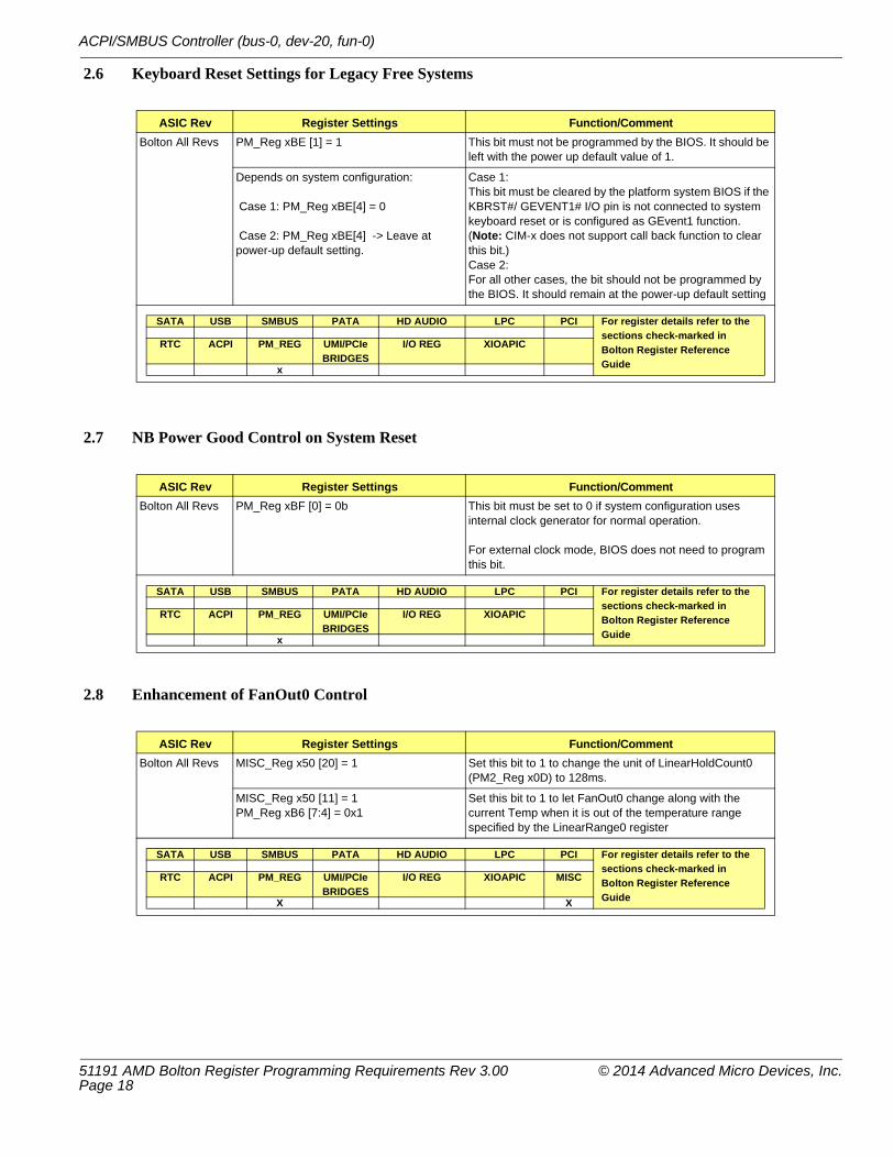
2.6 Keyboard Reset Settings for Legacy Free Systems
2.7 NB Power Good Control on System Reset
2.8 Enhancement of FanOut0 Control
ASIC Rev Register Settings Function/CommentBolton All Revs PM_Reg xBE [1] = 1 This bit must not be programmed by the BIOS. It should be
left with the power up default value of 1.
Depends on system configuration: Case 1: PM_Reg xBE[4] = 0
Case 2: PM_Reg xBE[4] -> Leave at power-up default setting.
Case 1: This bit must be cleared by the platform system BIOS if the KBRST#/ GEVENT1# I/O pin is not connected to system keyboard reset or is configured as GEvent1 function. (Note: CIM-x does not support call back function to clear this bit.)Case 2: For all other cases, the bit should not be programmed by the BIOS. It should remain at the power-up default setting
ASIC Rev Register Settings Function/CommentBolton All Revs PM_Reg xBF [0] = 0b This bit must be set to 0 if system configuration uses
internal clock generator for normal operation.
For external clock mode, BIOS does not need to program this bit.
ASIC Rev Register Settings Function/CommentBolton All Revs MISC_Reg x50 [20] = 1 Set this bit to 1 to change the unit of LinearHoldCount0
(PM2_Reg x0D) to 128ms.
MISC_Reg x50 [11] = 1PM_Reg xB6 [7:4] = 0x1
Set this bit to 1 to let FanOut0 change along with the current Temp when it is out of the temperature range specified by the LinearRange0 register
SATA USB SMBUS PATA HD AUDIO LPC PCI For register details refer to the sections check-marked in Bolton Register Reference Guide
RTC ACPI PM_REG UMI/PCIe
BRIDGESI/O REG XIOAPIC
x
SATA USB SMBUS PATA HD AUDIO LPC PCI For register details refer to the sections check-marked in Bolton Register Reference Guide
RTC ACPI PM_REG UMI/PCIe
BRIDGESI/O REG XIOAPIC
x
SATA USB SMBUS PATA HD AUDIO LPC PCI For register details refer to the sections check-marked in Bolton Register Reference Guide
RTC ACPI PM_REG UMI/PCIe
BRIDGESI/O REG XIOAPIC MISC
X X
51191 AMD Bolton Register Programming Requirements Rev 3.00 © 2014 Advanced Micro Devices, Inc.Page 18

ACPI/SMBUS Controller (bus-0, dev-20, fun-0)
2.9 Extend SerIrq Request
2.10 Mt C1e Enable
Note: The programming below is required when Mt C1e is enabled on the CPU side.
2.11 HWM Sensor CLK
ASIC Rev Register Settings Function/CommentBolton All Revs MISC_Reg x50 [29] = 1 Set this bit to 1 to extend SerIrq request from device in
order to participate in ClkRun# protocol.
ASIC Rev Register Settings Function/CommentBolton All Revs PM_Reg x7A[15] = 1
PM_Reg x7A[3:0] = xxxxbSet bit 15 to 1 to enable Mt C1e message decoding. When this is enabled, FCH will monitor HALT message(s) coming from CPU and initiate C1e. For the case of multiple package CPUs, each package CPU will issue its own HALT message and FCH will collect all HALT messages before it initiates C1e. Bits [3:0] specify the number of HALT messages that FCH should monitor.
PM_Reg 0x80[13] = 1PM_Reg 0x80[7] = 1
Set to 1 to enable Mt C1e protocol.
ASIC Rev Register Settings Function/CommentBolton All Revs PM2_Reg xEF [3:0] = 0xA
PM2_Reg xFF [1:0] = 0x2These settings are required to make HWM work properly.
SATA USB SMBUS PATA HD AUDIO LPC PCI For register details refer to the sections check-marked in Bolton Register Reference Guide
RTC ACPI PM_REG UMI/PCIe
BRIDGESI/O REG XIOAPIC MISC
X
SATA USB SMBUS PATA HD AUDIO LPC PCI For register details refer to the sections check-marked in Bolton Register Reference Guide
RTC ACPI PM_REG UMI/PCIe
BRIDGESI/O REG XIOAPIC MISC
X
SATA USB SMBUS PATA HD AUDIO LPC PCI For register details refer to the sections check-marked in Bolton Register Reference Guide
RTC ACPI PM2_REG UMI/PCIe
BRIDGESI/O REG XIOAPIC MISC
X
© 2014 Advanced Micro Devices, Inc. 51191 AMD Bolton Register Programming Requirements Rev 3.00 Page 19

ACPI/SMBUS Controller (bus-0, dev-20, fun-0)
2.12 Clear Status of SATA PERR
2.13 Enable Delayed SLP_S3/S5 to Motherboard
2.14 Enable C-State Wake-up before Warm Reset
2.15 Enable DMAACTIVE#
ASIC Rev Register Settings Function/CommentBolton All Revs Write 1 to clear SMI_Reg x3C [6]
Write 1 to clear SMI_Reg x86 [7]BIOS should write a '1' to both registers to reset the SATA PERR status soon after a cold boot, warm boot and any S3/S1 resume events. The registers should also be written if the BIOS initiates a write to the CF9 register outside a warm boot event. (This programming should be done before any SATA activity is initiated).
ASIC Rev Register Settings Function/CommentBolton All Revs PM_Reg xC1 [2] = 1 Set 1 to delay SLP_S3# and SLP_S5# to the board.
This will allow the internal logic to put signals into the correct state before turning off the S0 power.
ASIC Rev Register Settings Function/CommentBolton All Revs PM_Reg xBE [0] = 1 When this bit is 1, FCH will generate a break event to wake
up the CPU from C-state before every warm reset.Note: This is required for C1e, unnecessary for Fusion.
ASIC Rev Register Settings Function/CommentBolton All Revs PM_Reg x7F[0] = 1 Set this bit to 1 to allow FCH to drive the DMAACTIVE#
signal to APU to report DMA Activity in progress on downstream devices. This bit should only be set for the APU/CPU that support this feature. Please refer to the APU/CPU documentation for further information.
SATA USB SMBUS PATA HD AUDIO LPC PCI For register details refer to the sections check-marked in Bolton Register Reference Guide
XRTC ACPI PM_REG UMI/PCIe
BRIDGESI/O REG XIOAPIC MISC
SATA USB SMBUS PATA HD AUDIO LPC PCI For register details refer to the sections check-marked in Bolton Register Reference Guide
RTC ACPI PM_REG UMI/PCIe
BRIDGESI/O REG XIOAPIC MISC
X
SATA USB SMBUS PATA HD AUDIO LPC PCI For register details refer to the sections check-marked in Bolton Register Reference Guide
RTC ACPI PM_REG UMI/PCIe
BRIDGESI/O REG XIOAPIC MISC
X
SATA USB SMBUS PATA HD AUDIO LPC PCI For register details refer to the sections check-marked in Bolton Register Reference Guide
RTC ACPI PM_REG UMI/PCIe
BRIDGESI/O REG XIOAPIC MISC
X
51191 AMD Bolton Register Programming Requirements Rev 3.00 © 2014 Advanced Micro Devices, Inc.Page 20

ACPI/SMBUS Controller (bus-0, dev-20, fun-0)
2.16 IMC Enable
2.17 Adjust PM Timer Read Mechanism
2.18 PCIe® Wake Status and PME Wake Status
2.19 Set RTC OSC Output Drive
ASIC Rev Register Settings Function/CommentBolton All Revs Misc_Reg x80[2] = 1 When this bit is 1, IMC is enabled and running. IMC can be
enabled by hardware strap or by software strap bits (by setting Misc_Reg 0x84 bit[31] and bit[2] to 1, and then performing a PCI reset)
ASIC Rev Register Settings Function/CommentBolton All Revs Misc_Reg x51[0] = 1 Set this bit to '1' to prevent ACPI logic to select incorrect
PM timer data source when there is concurrent DMA write traffic from downstream devices.
ASIC Rev Register Settings Function/CommentBolton All Revs AcpiPmEvtBlk: x00[15:14] = 0 Clear PciExpWakeStatus and WakeStatus bits before
entering sleep state.
When PCIe wake is enabled, care must taken to ensure both of the status bits are cleared before entering into sleep states. Not clearing these status bits could result in the system either waking up immediately or failing to wake up from sleep states.
ASIC Rev Register Settings Function/CommentBolton All Revs PM_Reg x57[1,0] = 11b Clamp the RTC OSC drive to high output.
SATA USB SMBUS PATA HD AUDIO LPC PCI For register details refer to the sections check-marked in Bolton Register Reference Guide
RTC ACPI PM_REG UMI/PCIe
BRIDGESI/O REG XIOAPIC MISC
X
SATA USB SMBUS PATA HD AUDIO LPC PCI For register details refer to the sections check-marked in Bolton Register Reference Guide
RTC ACPI PM_REG UMI/PCIe
BRIDGESI/O REG XIOAPIC MISC
X
SATA USB SMBUS PATA HD AUDIO LPC PCI For register details refer to the sections check-marked in Bolton Register Reference Guide
RTC ACPI PM_REG UMI/PCIe
BRIDGESI/O REG XIOAPIC MISC
X X
SATA USB SMBUS PATA HD AUDIO LPC PCI For register details refer to the sections check-marked in Bolton Register Reference Guide
RTC ACPI PM_REG UMI/PCIe
BRIDGESI/O REG XIOAPIC MISC
X
© 2014 Advanced Micro Devices, Inc. 51191 AMD Bolton Register Programming Requirements Rev 3.00 Page 21

ACPI/SMBUS Controller (bus-0, dev-20, fun-0)
51191 AMD Bolton Register Programming Requirements Rev 3.00 © 2014 Advanced Micro Devices, Inc.Page 22

LPC Controller (bus-0, dev-20, fun-3)
3 LPC Controller (bus-0, dev-20, fun-3)
3.1 SPI Controller MMIO Base Address
3.2 Enable SPI ROM Prefetch
3.3 Enable LPC DMA Function
ASIC Rev Register Settings Function/CommentBolton All Revs LPC_PCI_Config 0xA0 [31:5] Memory base address for SPI ROM control registers.
SBIOS needs to program non-zero address value to enable the MMIO access.
ASIC Rev Register Settings Function/CommentBolton All Revs LPC_PCI_Config 0xBB [0] = 1 Enable SPI ROM (64 bytes) prefetch for host access
LPC_PCI_Config 0xBA [7] = 1 Enable SPI ROM (64 bytes) prefetch for usb access
LPC_PCI_Config 0xBA [2] = 1 Enable SPI ROM (64 bytes) prefetch for IMC access. The bit can be programmed by IMC only.
ASIC Rev Register Settings Function/CommentBolton All Revs PM_Reg 0x04 [8] = 1 (only when the
system is in non-DOS mode)This is applicable to non-DOS mode only.Enables legacy DMA prefetch enhancement for channel 0, 1, 2, and 3. This bit should be set to improve DMA out (e.g. memory-to-floppy disk) performance.
Note: This bit should only be enabled in the ACPI method (called by the OS). This ensures that it is enabled only when the system is in Windows® mode. Under DOS mode, this feature may not work properly and may cause the floppy to malfunction.
LPC_PCI_Config 0x40 [2] = 1
LPC_PCI_Config 0x78 [0] = 1
PM_Reg 0x08 [0] = 1
Set these bits to make LPC DMA work properly. This is only needed if DMA function is required on the LPC interface. Note: LPC_PCI_Config 0x78[3:2] has to be programmed to enable the Ldrq0/Ldrq1 input.
SATA USB SMBUS PATA HD AUDIO LPC PCI For register details refer to the sections check-marked in Bolton Register Reference Guide
XRTC ACPI PM REG UMI/PCIe
BRIDGESI/O REG XIOAPIC
SATA USB SMBUS PATA HD AUDIO LPC PCI For register details refer to the sections check-marked in Bolton Register Reference Guide
XRTC ACPI PM REG UMI/PCIe
BRIDGESI/O REG XIOAPIC
SATA USB SMBUS PATA HD AUDIO LPC PCI For register details refer to the sections check-marked in Bolton Register Reference Guide
XRTC ACPI PM REG UMI/PCIe
BRIDGESI/O REG XIOAPIC
© 2014 Advanced Micro Devices, Inc. 51191 AMD Bolton Register Programming Requirements Rev 3.00 Page 23

LPC Controller (bus-0, dev-20, fun-3)
3.4 Enable ClkRun Function
3.5 Enable LPCCLK0 Power-Down Function
3.6 Disable LPC A-Link Cycle Bypass
3.7 LPC Cycle Abort Sync Threshold Setting
ASIC Rev Register Settings Function/CommentBolton All Revs LPC_PCI_Config 0xBB [2] = 1
LPC_PCI_Config 0xD0 [2] = 0(default)
Allow LpcClk0/LpcClk1 to stop under ClkRun# protocol
ASIC Rev Register Settings Function/CommentBolton All Revs PM_Reg 0xD2 [3] = 1 Set to 1 to enable LPCCLK0 power-down (driven to 0)
when the following are true:- IMC is not enabled- System is in S3 or S5This will prevent leakage on LPCCLK0 during S3/S5.
ASIC Rev Register Settings Function/CommentBolton All Revs MISC_Reg 0x50 [19] = 1 Tells the A-Link that the LPC cycle should not be bypassed
when a retry has timed out
ASIC Rev Register Settings Function/CommentBolton All Revs LPC_PCI_Config 0xBB[3] = 1 Set this bit to 1 to allow LPC controller to abort cycle if it
observes three consecutive clocks without a defined SYNC.
Default = 0 LPC controller will abort cycle if it observes two consecutive clocks without a defined SYNC.
SATA USB SMBUS PATA HD AUDIO LPC PCI For register details refer to the sections check-marked in Bolton Register Reference Guide
XRTC ACPI PM REG UMI/PCIe
BRIDGESI/O REG XIOAPIC
SATA USB SMBUS PATA HD AUDIO LPC PCI For register details refer to the sections check-marked in Bolton Register Reference Guide
XRTC ACPI PM REG UMI/PCIe
BRIDGESI/O REG XIOAPIC
SATA USB SMBUS PATA HD AUDIO LPC PCI For register details refer to the sections check-marked in Bolton Register Reference Guide
XRTC ACPI PM REG UMI/PCIe
BRIDGESI/O REG XIOAPIC
SATA USB SMBUS PATA HD AUDIO LPC PCI For register details refer to the sections check-marked in Bolton Register Reference Guide
XRTC ACPI PM REG UMI/PCIe
BRIDGESI/O REG XIOAPIC
51191 AMD Bolton Register Programming Requirements Rev 3.00 © 2014 Advanced Micro Devices, Inc.Page 24

UMI and A/B-Link Settings - Indirect I/O Access
4 UMI and A/B-Link Settings - Indirect I/O Access
4.1 Defining AB_REG_BAR
4.2 Upstream DMA Access
4.3 PCIB Prefetch Settings
ASIC Rev Register Settings Function/CommentBolton All Revs PM_Reg 0xE0 [31:0] = ABRegBar Defines the AB I/O base address.
Refer to Bolton Register Reference Guide, Chapter 5: UMI/PCIe Bridges for more information.
ASIC Rev Register Settings Function/CommentBolton All Revs AXCFG_Reg: 0x04 [2] = 1 Enable Bolton to issue memory read/write requests in the
upstream direction.
Programming Sequence:
OUT AB_INDX, 0x80000004 // Load AB_INDX with pointer to AXCFG_Reg:0x04IN AB_DATA, TMP // Read COMMAND register (AXCFG_Reg:0x04)OR TMP, 0x00000004 // Set bit 4OUT AB_DATA, TMP // Set BUS_MASTER_EN
ASIC Rev Register Settings Function/CommentBolton All Revs PCIB prefetch
ABCFG_Reg 0x10060 [20] = 1ABCFG_Reg 0x10064 [20] = 1
The settings on AB control the PCIB prefetch. For all revisions the prefetch needs to be enabled for performance enhancement.
SATA USB SMBUS PATA HD AUDIO LPC PCI For register details refer to the sections check-marked in Bolton Register Reference Guide
RTC ACPI PM REG UMI/PCIe
BRIDGESI/O REG XIOAPIC
X
SATA USB SMBUS PATA HD AUDIO LPC PCI For register details refer to the sections check-marked in Bolton Register Reference Guide
RTC ACPI PM REG UMI/PCIe
BRIDGESI/O REG XIOAPIC
X
SATA USB SMBUS PATA AC97 HD AUDIO LPC PCI For register details refer to the sections check-marked in Bolton Register Reference Guide
RTC ACPI PM REG UMI/PCIe
BRIDGESI/O REG XIOAPIC
X
© 2014 Advanced Micro Devices, Inc. 51191 AMD Bolton Register Programming Requirements Rev 3.00 Page 25

UMI and A/B-Link Settings - Indirect I/O Access
4.4 OHCI Prefetch Settings
4.5 B-Link Client’s Credit Variable Settings for the Downstream Arbitration Equation
4.6 Setting B-Link Prefetch Mode
4.7 Detection of Upstream Interrupts
ASIC Rev Register Settings Function/CommentBolton All Revs ABCFG_Reg 0x80 [0] = 1 This register in AB controls the USB OHCI controller
prefetch used for enhancing performance of ISO out devices.
ASIC Rev Register Settings Function/CommentBolton All Revs ABCFG_Reg 0x9C [0] = 1 Disable the credit variable in the downstream arbitration
equation.
ASIC Rev Register Settings Function/CommentBolton All Revs ABCFG_Reg 0x80 [18:17] = 0x3 Set B-Link prefetch mode.
ASIC Rev Register Settings Function/CommentBolton All Revs ABCFG_Reg 0x94 [20] = 1
ABCFG_Reg 0x94 [19:0] = CPU interrupt delivery address [39:20].
Enable UMI logic to detect upstream interrupts for the purposes of system management.
SATA USB SMBUS PATA HD AUDIO LPC PCI For register details refer to the sections check-marked in Bolton Register Reference Guide
RTC ACPI PM REG UMI/PCIe
BRIDGESI/O REG XIOAPIC
X
SATA USB SMBUS PATA HD AUDIO LPC PCI For register details refer to the sections check-marked in Bolton Register Reference Guide
RTC ACPI PM REG UMI/PCIe
BRIDGESI/O REG XIOAPIC
X
SATA USB SMBUS PATA HD AUDIO LPC PCI For register details refer to the sections check-marked in Bolton Register Reference Guide
RTC ACPI PM REG UMI/PCIe
BRIDGESI/O REG XIOAPIC
X
SATA USB SMBUS PATA HD AUDIO LPC PCI For register details refer to the sections check-marked in Bolton Register Reference Guide
RTC ACPI PM REG UMI/PCIe
BRIDGESI/O REG XIOAPIC
X
51191 AMD Bolton Register Programming Requirements Rev 3.00 © 2014 Advanced Micro Devices, Inc.Page 26

UMI and A/B-Link Settings - Indirect I/O Access
4.8 Downstream Posted Transactions to Pass Non-Posted Transactions
4.9 AB and UMI/GPP Clock Gating
4.10 AB Int_Arbiter Enhancement
4.11 Requester ID
ASIC Rev Register Settings Function/CommentBolton All Revs ABCFG_Reg 0x10090 [8] = 1 Enable downstream posted transactions to pass non-
posted transactions.
ASIC Rev Register Settings Function/CommentBolton All Revs ABCFG_Reg 0x54 [23:16] = 0x4
ABCFG_Reg 0x10054 [23:16] = 0x4ABCFG_Reg 0x98 [15:12] = 0x4
Program the number of cycles to delay before gating AB and UMI/GPP clocks after idle condition.
ABCFG_Reg 0x54 [24] = 1ABCFG_Reg 0x10054 [24] = 1ABCFG_Reg 0x98 [11:8] = 0x7
Enable AB and UMI/GPP clock-gating.
ABCFG_Reg 0x90 [0] = 1 Enable UMI TXCLK gating
ASIC Rev Register Settings Function/CommentBolton All Revs ABCFG_Reg 0x10054 [11:0] = 0x7FF Enable the A-Link int_arbiter enhancement to allow the A-
Link bandwidth to be used more efficiently.
ASIC Rev Register Settings Function/CommentBolton All Revs ABCFG_Reg 0x98 [16] = 1
ABCFG_Reg 0x98 [17] = 1Enable the requester ID for upstream traffic.[16]: for UMI link[17]: for GPP
SATA USB SMBUS PATA HD AUDIO LPC PCI For register details refer to the sections check-marked in Bolton Register Reference Guide
RTC ACPI PM REG UMI/PCIe
BRIDGESI/O REG XIOAPIC
X
SATA USB SMBUS PATA HD AUDIO LPC PCI For register details refer to the sections check-marked in Bolton Register Reference Guide
RTC ACPI PM_REG UMI/PCIe
BRIDGESI/O REG XIOAPIC
x
SATA USB SMBUS PATA HD AUDIO LPC PCI For register details refer to the sections check-marked in Bolton Register Reference Guide
RTC ACPI PM REG UMI/PCIe
BridgesI/O REG XIOAPIC
X
SATA USB SMBUS PATA HD AUDIO LPC PCI For register details refer to the sections check-marked in Bolton Register Reference Guide.
RTC ACPI PM REG UMI/PCIe
BridgesI/O REG XIOAPIC
X
© 2014 Advanced Micro Devices, Inc. 51191 AMD Bolton Register Programming Requirements Rev 3.00 Page 27

UMI and A/B-Link Settings - Indirect I/O Access
4.12 UMI LOs/L1 NAK Reduction
4.13 Power Saving Feature for UMI Lanes
4.14 Non-Posted Memory Write Support
ASIC Rev Register Settings Function/CommentBolton All Revs AXINDP_Reg 0xA0 [7:4] = 0x3 Enter L1 sooner after ACK’ing PM request. This is done to
reduce the number of NAK received with L1 enabled.
AXINDP_Reg 0xB1 [19] = 0x1 Turn off receiver when UMI Root Complex transmitter is in L0s.
AXINDP_Reg 0xB1 [28] = 0x1 Enables de-assertion of PG2RX_CR_EN to lock clock recovery parameter when lane is in electrical idle.0 = CR_EN is always asserted1 = CR_EN is de-asserted when RX_EN is de-asserted during L0s/L1 and inactive lanes
ASIC Rev Register Settings Function/CommentBolton All Revs ABCFG_Reg 0xB8 [30] = 1 Set this bit to 1 to allow for proper ASPM L1 and L0s
transitions when PLL power-down in L1 is enabled.This bit should be set before programming the sequence below to enable the PPL Power down mode.
AXINDC_Reg 0x40 [3] = 1AXINDC_Reg 0x40 [0] = 1AXINDC_Reg 0x40 [4] = 0AXINDC_Reg 0x40 [9] = 0AXINDC_Reg 0x40 [12] = 1
Enable PLL OFF during L1 state for power saving.Enable unused lane power down feature.Enable PLL Buffer power down during L1 state.Enable PLL to power down during L1 state.Enable PHY RX front end circuit to shut off during L1 when PLL power down is enabled.
AXINDC_Reg 0x02 [8] = 1 Enable fix for race problem between PLL calibrator and LC wake up from L1.
ASIC Rev Register Settings Function/CommentBolton All Revs AXINDC_Reg 0x10 [9] = 1 Enable Non-Posted Memory Write Support.
SATA USB SMBUS PATA HD AUDIO LPC PCI For register details refer to the sections check-marked in the Bolton Register Reference Guide.
RTC ACPI PM REG A-LINK I/O REG XIOAPIC
X
SATA USB SMBUS PATA HD AUDIO LPC PCI For register details refer to the sections check-marked in Bolton Register Reference Guide
RTC ACPI PM REG UMI/PCIe
BridgesI/O REG XIOAPIC
X
SATA USB SMBUS PATA HD AUDIO LPC PCI For register details refer to the sections check-marked in Bolton Register Reference Guide
RTC ACPI PM REG UMI/PCIe
BridgesI/O REG XIOAPIC
X
51191 AMD Bolton Register Programming Requirements Rev 3.00 © 2014 Advanced Micro Devices, Inc.Page 28

UMI and A/B-Link Settings - Indirect I/O Access
4.15 SMI Ordering
4.16 Posted Pass Non-Posted Feature
4.17 UMI Speed Change
ASIC Rev Register Settings Function/CommentBolton All Revs ABCFG_Reg 0x90 [21] = 1 SMI ordering enhancement enable
ASIC Rev Register Settings Function/CommentBolton All Revs ABCFG_Reg 0x10090 [12:10] = 0x07 Set retry limit.
ABCFG_Reg 0x58 [15:11] = 0x1C Set upstream non-posted threshold.ABCFG_Reg 0xB4 [1:0] = 0x03 Enable posted pass non-posted feature.
ASIC Rev Register Settings Function/CommentBolton All Revs Step 1:
AXINDP_Reg 0xA4 [0] = 0x1
Step 2:AXCFG_Reg 0x88 [3:0] = 0x2
Step3:AXINDP_Reg 0xA4 [18] = 0x1
To enable UMI link speed to go to, 2GB/s
SATA USB SMBUS PATA HD AUDIO LPC PCI For register details refer to the sections check-marked in Bolton Register Reference Guide
RTC ACPI PM REG UMI/PCIe
BridgesI/O REG XIOAPIC
X
SATA USB SMBUS PATA HD AUDIO LPC PCI For register details refer to the sections check-marked in Bolton Register Reference Guide
RTC ACPI PM REG UMI/PCIe
BridgesI/O REG XIOAPIC
X
SATA USB SMBUS PATA HD AUDIO LPC PCI For register details refer to the sections check-marked in Bolton Register Reference Guide
RTC ACPI PM REG UMI/PCIe
BridgesI/O REG XIOAPIC
X
© 2014 Advanced Micro Devices, Inc. 51191 AMD Bolton Register Programming Requirements Rev 3.00 Page 29
UMI and A/B-Link Settings - Indirect I/O Access
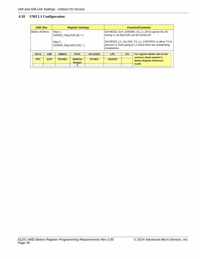
4.18 UMI L1 Configuration
ASIC Rev Register Settings Function/CommentBolton All Revs Step 1:
AXINDC_Reg 0x02 [0] = 1
Step 2:AXINDP_Reg 0x02 [15] = 1
Set REGS_DLP_IGNORE_IN_L1_EN to ignore DLLPs during L1 so that txclk can be turned off.
Set REGS_LC_ALLOW_TX_L1_CONTROL to allow TX to prevent LC from going to L1 when there are outstanding completions.
SATA USB SMBUS PATA HD AUDIO LPC PCI For register details refer to the sections check-marked in Bolton Register Reference Guide
RTC ACPI PM REG UMI/PCIe
BridgesI/O REG XIOAPIC
X
51191 AMD Bolton Register Programming Requirements Rev 3.00 © 2014 Advanced Micro Devices, Inc.Page 30
PCIe® General Purpose Ports
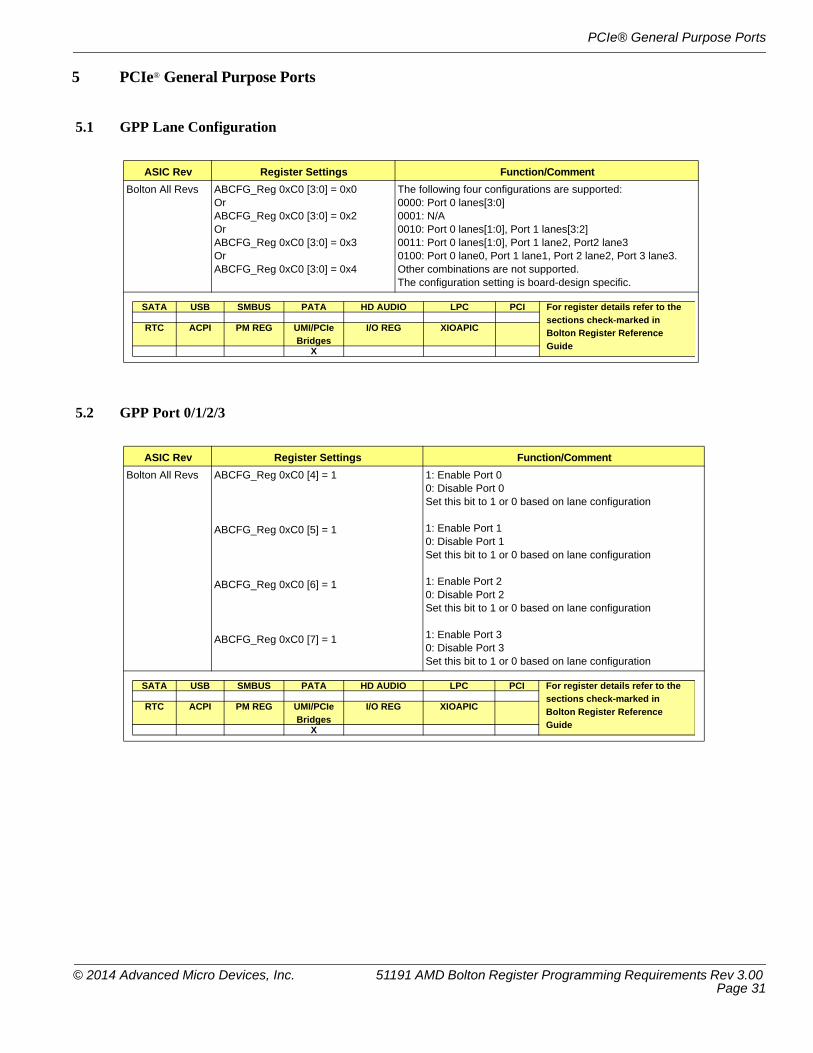
5 PCIe® General Purpose Ports
5.1 GPP Lane Configuration
5.2 GPP Port 0/1/2/3
ASIC Rev Register Settings Function/CommentBolton All Revs ABCFG_Reg 0xC0 [3:0] = 0x0
OrABCFG_Reg 0xC0 [3:0] = 0x2OrABCFG_Reg 0xC0 [3:0] = 0x3OrABCFG_Reg 0xC0 [3:0] = 0x4
The following four configurations are supported:0000: Port 0 lanes[3:0]0001: N/A0010: Port 0 lanes[1:0], Port 1 lanes[3:2]0011: Port 0 lanes[1:0], Port 1 lane2, Port2 lane30100: Port 0 lane0, Port 1 lane1, Port 2 lane2, Port 3 lane3.Other combinations are not supported.The configuration setting is board-design specific.
ASIC Rev Register Settings Function/CommentBolton All Revs ABCFG_Reg 0xC0 [4] = 1
ABCFG_Reg 0xC0 [5] = 1
ABCFG_Reg 0xC0 [6] = 1
ABCFG_Reg 0xC0 [7] = 1
1: Enable Port 00: Disable Port 0Set this bit to 1 or 0 based on lane configuration
1: Enable Port 10: Disable Port 1Set this bit to 1 or 0 based on lane configuration
1: Enable Port 20: Disable Port 2Set this bit to 1 or 0 based on lane configuration
1: Enable Port 30: Disable Port 3Set this bit to 1 or 0 based on lane configuration
SATA USB SMBUS PATA HD AUDIO LPC PCI For register details refer to the sections check-marked in Bolton Register Reference Guide
RTC ACPI PM REG UMI/PCIe
BridgesI/O REG XIOAPIC
X
SATA USB SMBUS PATA HD AUDIO LPC PCI For register details refer to the sections check-marked in Bolton Register Reference Guide
RTC ACPI PM REG UMI/PCIe
BridgesI/O REG XIOAPIC
X
© 2014 Advanced Micro Devices, Inc. 51191 AMD Bolton Register Programming Requirements Rev 3.00 Page 31

PCIe® General Purpose Ports
5.3 GPP Reset
ASIC Rev Register Settings Function/CommentBolton All Revs ABCFG_Reg 0xC0 [8] = 0 GPP lanes are in reset mode until the software writes 0 to
this register bit. The register should be programmed after software has enabled the GPP. Set this bit to 0 to release reset so all the GPP lane configurations can take effect.
If GPP is disabled or no devices are present, software needs to clear this bit to shut-down unused IO pads for additional power saving. Refer to "GPP Dynamic Power Saving" for more details.
PM_Reg 0xBF [4] = See Note This register should be used to de-assert the PCIe® reset to the device on GPP. * Note: Software should toggle PM_Reg 0xBF[4] just before the link is activated. The specification requires reset to be de-asserted 20 ms before link activity. Refer to
PCI Express® Specification Rev 2.1 for more details.
SATA USB SMBUS PATA HD AUDIO LPC PCI For register details refer to the sections check-marked in Bolton Register Reference Guide
RTC ACPI PM REG UMI/PCIe
BridgesI/O REG XIOAPIC
X X
51191 AMD Bolton Register Programming Requirements Rev 3.00 © 2014 Advanced Micro Devices, Inc.Page 32

PCIe® General Purpose Ports
5.4 PCIe® Ports De-emphasis Settings
5.5 Write Capability for PCIe® Read-Only Registers
ASIC Rev Register Settings Function/CommentBolton All Revs Port 0:
ABCFG_Reg 0x340 [21] = 1
Port 1: ABCFG_Reg 0x344 [21] = 1
Port 2: ABCFG_Reg 0x348 [21] = 1
Port 3: ABCFG_Reg 0x34C [21] = 1
For each port, poll RCINDP_Reg 0xA5[7:0];
If read back 0x10, no change.If read back 0x29 or 0x2A, clear de-emphasis bit for corresponding port, then toggle external PCIE_RST through GEVENT4.
Port 0: ABCFG_Reg 0x340 [21] = 0
Port 1: ABCFG_Reg 0x344 [21] = 0
Port 2: ABCFG_Reg 0x348 [21] = 0
Port 3: ABCFG_Reg 0x34C [21] = 0
0: -6dB de-emphasis for Port 01: -3.5dB de-emphasis for Port 0
0: -6dB de-emphasis for Port 11: -3.5dB de-emphasis for Port 1
0: -6dB de-emphasis for Port 21: -3.5dB de-emphasis for Port 2
0: -6dB de-emphasis for Port 31: -3.5dB de-emphasis for Port 3
ASIC Rev Register Settings Function/CommentBolton All Revs RCINDC_Reg 0x10 [0] = 1
ABCFG_Reg 0x330 [10] = 0SBIOS needs to set this bit to disable the writable function
of the PCIe® read-only registers.
SATA USB SMBUS PATA HD AUDIO LPC PCI For register details refer to the sections check-marked in Bolton Register Reference Guide
RTC ACPI PM REG UMI/PCIe
BridgesI/O REG XIOAPIC
X
SATA USB SMBUS PATA HD AUDIO LPC PCI For register details refer to the sections check-marked in Bolton Register Reference Guide
RTC ACPI PM REG UMI/PCIe
BridgesI/O REG XIOAPIC
X
© 2014 Advanced Micro Devices, Inc. 51191 AMD Bolton Register Programming Requirements Rev 3.00 Page 33

PCIe® General Purpose Ports
5.6 Serial Number Capability
5.7 Multi-function Enable
5.8 GPP Upstream Memory Write Arbitration Enhancement
5.9 GPP Memory Write Max Payload Improvement
ASIC Rev Register Settings Function/CommentBolton All Revs ABCFG_Reg 0x330 [26] = 0 Disable serial number capability
ASIC Rev Register Settings Function/CommentBolton All Revs ABCFG_Reg 0x90 [20] = 1 Enable GPP bridge multi-function.
ASIC Rev Register Settings Function/Comment
Bolton All Revs ABCFG_Reg 0x54 [26] = 1 Arbitration enhancement for GPP specific traffic
ASIC Rev Register Settings Function/Comment
Bolton All Revs RCINDC_Reg 0x10 [12:10] = 0x4 Set Memory Write transfer to chip with 64 byte maximum payload
SATA USB SMBUS PATA HD AUDIO LPC PCI For register details refer to the sections check-marked in Bolton Register Reference Guide
RTC ACPI PM REG UMI/PCIe
BridgesI/O REG XIOAPIC
X
SATA USB SMBUS PATA HD AUDIO LPC PCI For register details refer to the sections check-marked in Bolton Register Reference Guide
RTC ACPI PM REG UMI/PCIe
BridgesI/O REG XIOAPIC
X
SATA USB SMBUS PATA HD AUDIO LPC PCI For register details refer to the sections check-marked in Bolton Register Reference Guide
RTC ACPI PM REG UMI/PCIe
BridgesI/O REG XIOAPIC
X
SATA USB SMBUS PATA HD AUDIO LPC PCI For register details refer to the sections check-marked in Bolton Register Reference Guide
RTC ACPI PM REG UMI/PCIe
BridgesI/O REG XIOAPIC
X
51191 AMD Bolton Register Programming Requirements Rev 3.00 © 2014 Advanced Micro Devices, Inc.Page 34

PCIe® General Purpose Ports
5.10 Multiple GPP Device Support
5.11 Separate Control for Release from Reset and Hold Training for each GPP Port
5.12 GPP PCIe® Native Interrupt Support
ASIC Rev Register Settings Function/CommentBolton All Revs ABCFG_Reg 0xF0 [2] = 1 Multiple GPP device traffic support when UR happens.
ASIC Rev Register Settings Function/CommentBolton All Revs ABCFG_Reg 0xC0 [12] = 0
ABCFG_Reg 0xC0 [13] = 0ABCFG_Reg 0xC0 [14] = 0ABCFG_Reg 0xC0 [15] = 0
Port 0 will be released from reset and hold training Port 1 will be released from reset and hold trainingPort 2 will be released from reset and hold trainingPort 3 will be released from reset and hold training
BIOS determines when to release when doing training sequences. If the port is not used, BIOS needs to set the hold_training to 0x1 for corresponding port.
ASIC Rev Register Settings Function/CommentBolton All Revs PCIe Cfg 0x3D [7:0] = 0x01 Enable GPP PCIe® native interrupt support.
GPP bridge pci cfg space 0x3DProgram these bits before RCINDC_Reg 0x10 [0] = 1 is programmed.
SATA USB SMBUS PATA HD AUDIO LPC PCI For register details refer to the sections check-marked in Bolton Register Reference Guide
RTC ACPI PM REG UMI/PCIe
BridgesI/O REG XIOAPIC
X
SATA USB SMBUS PATA HD AUDIO LPC PCI For register details refer to the sections check-marked in Bolton Register Reference Guide
RTC ACPI PM REG UMI/PCIe
BridgesI/O REG XIOAPIC
X
SATA USB SMBUS PATA HD AUDIO LPC PCI For register details refer to the sections check-marked in Bolton Register Reference Guide
RTC ACPI PM REG UMI/PCIe
BridgesI/O REG XIOAPIC
X
© 2014 Advanced Micro Devices, Inc. 51191 AMD Bolton Register Programming Requirements Rev 3.00 Page 35

PCIe® General Purpose Ports
5.13 GPP Error Reporting Configuration
5.14 Hot Plug: PCIe® Native Support
5.15 Link Bandwidth Notification Capability Enable
ASIC Rev Step Register Settings Function/CommentBolton All Revs 1 If GPP enabled
Port 0, 1, 2, 3:RCINDP_Reg 0x6A [1] = 0x0
Set error reporting mode to "first detected".
2 If AER disabledABCFG_Reg 0xF0 [1] = 0x0
Disable Address Translation cycle filtering.
Bolton All Revs 3 ABCFG_Reg 0xB8 [8] = 1ABCFG_Reg 0xB8 [26:24] = 0x5ABCFG_Reg 0xB8 [28] = 1
Configure upstream PCIe® message handling.
ASIC Rev Step Register Settings Function/CommentBolton All Revs 1 RCINDP_Reg 0x10 [3] = 0x1 Enable native PME.
2 PCIe_Cfg 0x5A [8] = 0x1 For slot which supports hot plug, “Slot Implemented” bit needs to be set to 1.This bit is HwInit.
3 PCIe_Cfg 0x6C [6] = 0x1. Report Hot-Plug Capable.This bit is HwInit.
4 RCINDP_Reg 0x20 [19] = 0x0 Enable flushing TLPs when Data Link is down.
ASIC Rev Register Settings Function/CommentBolton All Revs RCINDC 0xC1 [0] = 1
PCIe Cfg 0x68 [10] = 0
PCIe Cfg 0x68 [11] = 0
Enable GPP Link Bandwidth Notification Capability.
Link Bandwidth Management Interrupt Enable default value needs to be set to 0b for all GPP Root Ports’ PCI cfg space.
Link Autonomous Bandwidth Interrupt Enable default value needs to be set to 0b for all GPP Root Ports’ PCI cfg space.
SATA USB SMBUS PATA HD AUDIO LPC PCI For register details refer to the sections check-marked in Bolton Register Reference Guide
RTC ACPI PM REG UMI/PCIe
BridgesI/O REG XIOAPIC
X
SATA USB SMBUS PATA HD AUDIO LPC PCI For register details refer to the sections check-marked in Bolton Register Reference Guide
RTC ACPI PM REG UMI/PCIe
BridgesI/O REG XIOAPIC
X
SATA USB SMBUS PATA HD AUDIO LPC PCI For register details refer to the sections check-marked in Bolton Register Reference Guide
RTC ACPI PM REG UMI/PCIe
BridgesI/O REG XIOAPIC
X
51191 AMD Bolton Register Programming Requirements Rev 3.00 © 2014 Advanced Micro Devices, Inc.Page 36

PCIe® General Purpose Ports
5.16 Power Saving Feature for GPP Lanes
5.17 GPP L1 PM Request NAK Reduction
ASIC Rev Register Settings Function/Comment
If any GPP lanes are not used, they should be programmed to enable the Power Saving feature to minimize power consumption.Bolton All Revs RCINDC_Reg 0x40 [0] = 1
RCINDC_Reg 0x40 [3] = 1 [Power mode]RCINDC_Reg 0x40 [3] = 0 [Nominal mode]
RCINDC_Reg 0x40 [4] = 0
RCINDC_Reg 0x40 [9] = 0
RCINDC_Reg 0x40 [12] = 1
Enable unused GPP lane power down feature
Enable PLL OFF during L1 stateDisable PLL OFF during L1 state
Enable PLL Buffer power down during L1 state
Enable PLL to power down during L1 state
Enable PHY RX Front end circuit to shut off during L1 when PLL power down is enabled
*Note: before accessing RCINDC_Reg, SBIOS needs to release GPP Reset first, refer to section GPP Reset
RCINDC_Reg 0x02 [8] = 1 Enable fix for the race problem between PLL callibrator and LC wake up from L1.
RCINDC_Reg 0x02 [3] = 1 Enable powering down PLLs in L1 for active lanes in the presence of one or more inactive.
ASIC Rev Step Register Settings Function/CommentBolton All Revs 1 Port 0, 1, 2, 3:
RCINDP_Reg 0xA0 [7:4] = 0x1Enter L1 sooner after ACK’ing PM request. This is done to reduce the number of NAK received with L1 enabled.
SATA USB SMBUS PATA HD AUDIO LPC PCI For register details refer to the sections check-marked in Bolton Register Reference Guide
RTC ACPI PM REG UMI/PCIe
BridgesI/O REG XIOAPIC
X
SATA USB SMBUS PATA HD AUDIO LPC PCI For register details refer to the sections check-marked in Bolton Register Reference Guide
RTC ACPI PM REG A-LINK I/O REG XIOAPIC
X
© 2014 Advanced Micro Devices, Inc. 51191 AMD Bolton Register Programming Requirements Rev 3.00 Page 37

PCIe® General Purpose Ports
5.18 GPP ASPM L1/L0s Enable
5.19 GPP Immediate Ack PM_Active_State_Request_L1
ASIC Rev Step Register Settings Function/CommentBolton All Revs 1 L0s enable:
PCIe_Cfg 0x68 [1:0] = 0x1
L1 enable:PCIe_Cfg 0x68 [1:0] = 0x2
L1/L0s enable:PCIe_Cfg 0x68 [1:0] = 0x3
PCIe_Cfg 0x68 is standard PCI configuration space. BIOS needs to program all the GPP ports based on the GPP port configuration.
2 In the EP device, follow the capability list to find the PCIe capability (capability ID = 0x10).LINK_CNTL[1:0] pcieConfigDev*:0x68 PM_CONTROL
Set bits [1:0] to 0x1 for L0s.Set bits [1:0] to 0x2 for L1Set bits [1:0] to 0x3 for L0s/L1
Enable Enpoint device to support L0s/L1.
3 RCINDC_Reg 0x02 [0] = 1 When L1 is enabled:
Set REGS_DLP_IGNORE_IN_L1_EN to ignore DLLPs during L1 so that txclk can be turned off.
4 RCINDP_Reg 0x02 [15] = 1 When L1 is enabled, for each enabled GPP Port 0, 1, 2, 3:
Set REGS_LC_ALLOW_TX_L1_CONTROL to allow TX to prevent LC from going to L1 when there are outstanding completions.
If GPP is enabled, the settings below must be programmed for all GPP ports.Bolton All Revs 1 Port 0, 1, 2, 3:
RCINDP_Reg 0xA0 [11:8] = 0x9Set GPP L0s inactivity timer to 10us.
2 Port 0, 1, 2, 3:RCINDP_Reg 0xA0 [15:12] = 0x6
Set GPP L1 inactivity timer to 40us.
ASIC Rev Register Settings Function/CommentIf any GPP lanes are used, they should be programmed to enable the IMMEDIATE_ACK feature to workaround any device that doesn't follow the ordering rule. Please also set the BIOS option (L1_IMMEDIATE_ACK) for all the ports. Default BIOS is to enable this L1_IMMEDIATE_ACK feature.
Bolton All Revs Port 0, 1, 2, 3:RCINDP_Reg 0xA0 [23] = 1
Always ACK an ASPM L1 entry DLLP (i.e., never generate PM_NAK)
SATA USB SMBUS PATA HD AUDIO LPC PCI For register details refer to the sections check-marked in Bolton Register Reference Guide
RTC ACPI PM REG UMI/PCIe
BridgesI/O REG XIOAPIC
X
SATA USB SMBUS PATA HD AUDIO LPC PCI For register details refer to the sections check-marked in Bolton Register Reference Guide
RTC ACPI PM REG UMI/PCIe
BridgesI/O REG XIOAPIC
X
51191 AMD Bolton Register Programming Requirements Rev 3.00 © 2014 Advanced Micro Devices, Inc.Page 38

PCIe® General Purpose Ports
5.20 GPP Dynamic Power Saving
ASIC Rev Step Register Settings Function/CommentBolton All Revs. 1 ABCFG_Reg 0xC0[8] = 0 Release GPP reset
2 If no device is present or if link training fails, disable the corresponding port.
Port 0 disable:ABCFG_Reg 0xC0 [12] = 1
Port 1 disable:ABCFG_Reg 0xC0 [13] = 1
Port 2 disable:ABCFG_Reg 0xC0 [14] = 1
Port 3 disable:ABCFG_Reg 0xC0 [15] = 1
Set hold_training for unused GPP ports.
3 Enable “GPP Endpoint L1/L0s (ASPM)” for all Endpoint devices attached to GPP.
Please refer to Section 5.18, “GPP ASPM L1/L0s Enable ”
4 Enable “PLL Power Down in UMI L1”
Please refer to Section 4.13, “Power Saving Feature for UMI Lanes”
5 Enable “PLL Power Down in GPP L1”
Please refer to Section 4.13, “Power Saving Feature for UMI Lanes”
6 ABCFG_Reg 0x90 [19] = 1ABCFG_Reg 0x90 [6] = 1
Enable PHY PLL Power Down for both NB/FCH and GPP
7 Use attached table (section 5.20.2) to disable RX/TX pads.Set corresponding bits to 1 to disable pads.
Disable TX and RX pads’ power for unused GPP ports.
8 If no devices are present or link training fails in all 4 GPP ports:
RCINDC_Reg 0x65 [27:16] = 0xCFF
Force B_PPLL_PDNB to disable PLL.Force B_PPLL_BUF_PDNB to disable 10x driver in PLL.Force B_PIMP_TX_PDNB to didsable TX impedance calibration pad.Force B_PIMP_TX_PDNB to disable RX impedance calibration pad.
SATA USB SMBUS PATA HD AUDIO LPC PCI For register details refer to the sections check-marked in the Bolton Register Reference Guide
RTC ACPI PM REG UMI/PCIe
BridgesI/O REG XIOAPIC
X
© 2014 Advanced Micro Devices, Inc. 51191 AMD Bolton Register Programming Requirements Rev 3.00 Page 39
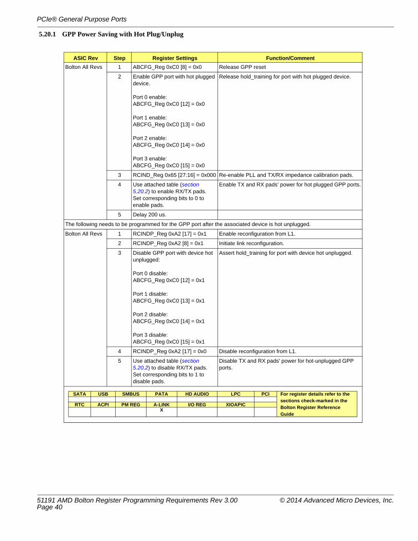
PCIe® General Purpose Ports
5.20.1 GPP Power Saving with Hot Plug/Unplug
ASIC Rev Step Register Settings Function/CommentBolton All Revs 1 ABCFG_Reg 0xC0 [8] = 0x0 Release GPP reset
2 Enable GPP port with hot plugged device.
Port 0 enable:ABCFG_Reg 0xC0 [12] = 0x0
Port 1 enable:ABCFG_Reg 0xC0 [13] = 0x0
Port 2 enable:ABCFG_Reg 0xC0 [14] = 0x0
Port 3 enable:ABCFG_Reg 0xC0 [15] = 0x0
Release hold_training for port with hot plugged device.
3 RCIND_Reg 0x65 [27:16] = 0x000 Re-enable PLL and TX/RX impedance calibration pads.
4 Use attached table (section 5.20.2) to enable RX/TX pads.Set corresponding bits to 0 to enable pads.
Enable TX and RX pads’ power for hot plugged GPP ports.
5 Delay 200 us.
The following needs to be programmed for the GPP port after the associated device is hot unplugged.
Bolton All Revs 1 RCINDP_Reg 0xA2 [17] = 0x1 Enable reconfiguration from L1.
2 RCINDP_Reg 0xA2 [8] = 0x1 Initiate link reconfiguration.
3 Disable GPP port with device hot unplugged:
Port 0 disable:ABCFG_Reg 0xC0 [12] = 0x1
Port 1 disable:ABCFG_Reg 0xC0 [13] = 0x1
Port 2 disable:ABCFG_Reg 0xC0 [14] = 0x1
Port 3 disable:ABCFG_Reg 0xC0 [15] = 0x1
Assert hold_training for port with device hot unplugged.
4 RCINDP_Reg 0xA2 [17] = 0x0 Disable reconfiguration from L1.
5 Use attached table (section 5.20.2) to disable RX/TX pads.Set corresponding bits to 1 to disable pads.
Disable TX and RX pads' power for hot-unplugged GPP ports.
SATA USB SMBUS PATA HD AUDIO LPC PCI For register details refer to the sections check-marked in the Bolton Register Reference Guide
RTC ACPI PM REG A-LINK I/O REG XIOAPIC
X
51191 AMD Bolton Register Programming Requirements Rev 3.00 © 2014 Advanced Micro Devices, Inc.Page 40
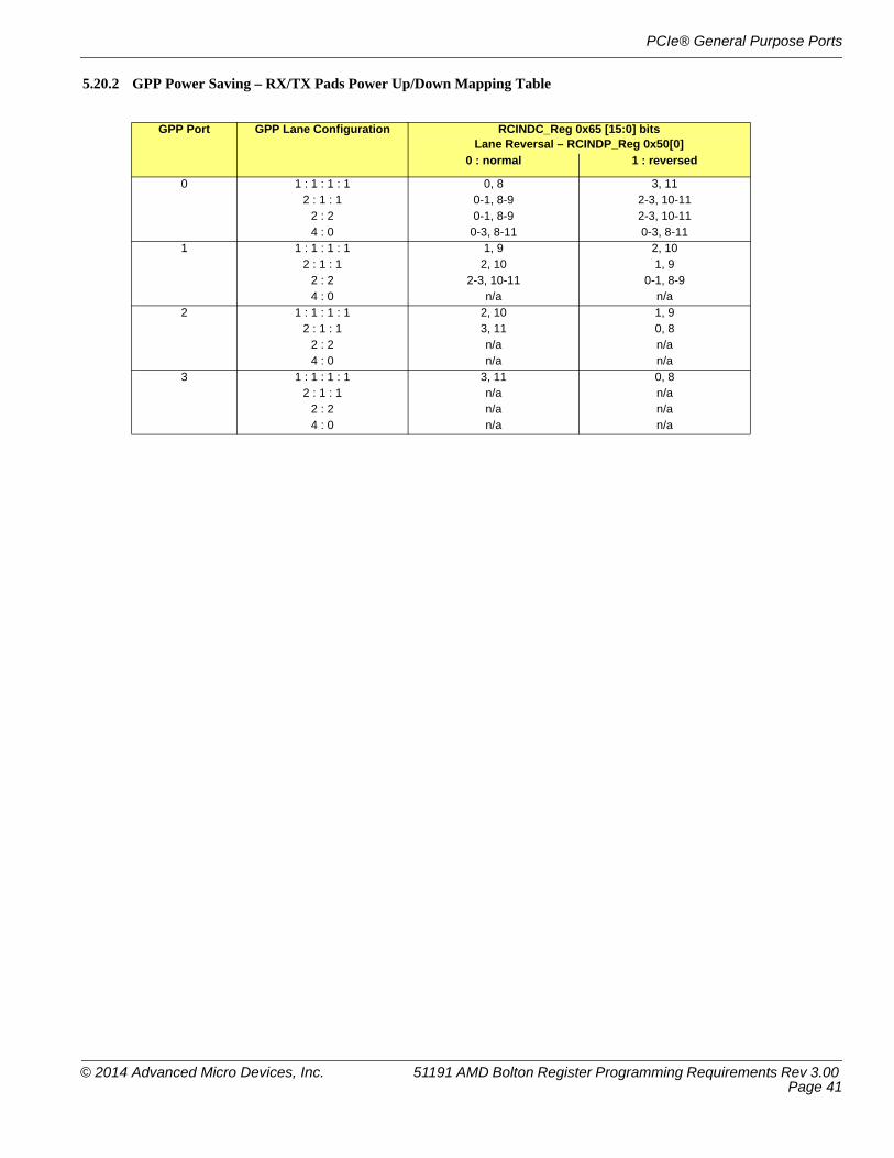
PCIe® General Purpose Ports
5.20.2 GPP Power Saving – RX/TX Pads Power Up/Down Mapping Table
GPP Port GPP Lane Configuration RCINDC_Reg 0x65 [15:0] bitsLane Reversal – RCINDP_Reg 0x50[0]
0 : normal 1 : reversed
0 1 : 1 : 1 : 1 0, 8 3, 112 : 1 : 1 0-1, 8-9 2-3, 10-11
2 : 2 0-1, 8-9 2-3, 10-114 : 0 0-3, 8-11 0-3, 8-11
1 1 : 1 : 1 : 1 1, 9 2, 102 : 1 : 1 2, 10 1, 9
2 : 2 2-3, 10-11 0-1, 8-94 : 0 n/a n/a
2 1 : 1 : 1 : 1 2, 10 1, 92 : 1 : 1 3, 11 0, 8
2 : 2 n/a n/a4 : 0 n/a n/a
3 1 : 1 : 1 : 1 3, 11 0, 82 : 1 : 1 n/a n/a
2 : 2 n/a n/a4 : 0 n/a n/a
© 2014 Advanced Micro Devices, Inc. 51191 AMD Bolton Register Programming Requirements Rev 3.00 Page 41

PCIe® General Purpose Ports
5.21 GPP Gen2 Speed Change
ASIC Rev Register Settings Function/CommentBolton All Revs. If
(Allow Gen2) AND (Gen2 is enabled) AND (GPP port is enabled)
Step 1:PCIe_Cfg 0x88 [3:0] = 0x2
Step 2:RCINDP_Reg 0xA4 [0] = 0x1
Step 3:RCINDP_Reg 0xA2 [13] = 0x0
Step 4:RCINDP_Reg 0xC0 [15] = 0x0
Step 5:RCINDP_Reg 0xA4 [29] = 0x1
If (GPP Compliance Pattern Mode disabled)
Step 6:Poll for RCINDP_Reg 0xA5 [5:0] == 0x10, every 400 us for maximum of 501 times.If timed out, proceed with Step 7, else exit.
Step 7:PCIe_Cfg 0x88 [3:0] = 0x1
Step 8:RCINDP_Reg 0xA4 [0] = 0x0
Step 9:RCINDP_Reg 0xA2 [13] = 0x1
If Gen2 is allowed via efuse setting, Gen2’s CMOS setting is enabled and GPP port is enabled, then proceed to program link to support Gen2.
Set Target Link Speed in Link Control 2 register to 5.0 GT/s.
Enable PCIe® Gen2.
Disable PCIe 2.0 defined link width change feature.
Disable RC auto speed negotiation.
Allow upstream component to automatically initiate multiple speed changes.
If GPP is NOT in compliance pattern testing mode, proceed with auto speed downgrade if device cannot enter Gen2.
If Gen2 is enabled and link fails to enter L0, then program link to Gen1 speed.
Set PCIe config space target link speed to Gen1.
Disable Gen2.
Disable link up configuration.
RCINDP_Reg needs to be programmed for each enabled GPP port.
PCIe_Cfg 0x88 is standard PCI configuration space. BIOS will need to program all the GPP ports based on the GPP port configuration.
SATA USB SMBUS PATA HD AUDIO LPC PCI For register details refer to the sections check-marked in the Bolton Register Reference Guide
RTC ACPI PM REG A-LINK I/O REG XIOAPIC
X
51191 AMD Bolton Register Programming Requirements Rev 3.00 © 2014 Advanced Micro Devices, Inc.Page 42

PCIB (PCI-bridge, bus-0, dev-20, fun-04)
6 PCIB (PCI-bridge, bus-0, dev-20, fun-04)
6.1 PCI-bridge Subtractive Decode
6.2 PCI-bridge Upstream Dual Address Window
6.3 One-Channel Mode
ASIC REV Register Settings Function/CommentBolton All Revs PCIB_PCI_Config 0x40 [5] = 1
PCIB_PCI_Config 0x4B [7] = 1Enable the PCI-bridge subtractive decode.This setting is strongly recommended since it supports some legacy PCI add-on cards.
ASIC REV Register Settings Function/CommentBolton All Revs PCIB_PCI_Config 0x50 [0] = 1 PCI-bridge upstream dual address window.
This setting is applicable if the system memory is more than 4GB, and the PCI devices can support dual address access.
ASIC REV Register Settings Function/CommentBolton All Revs PCIB_PCI_Config 0x64 [20] = 1 Enable One-Channel Mode for upstream read.
Note: This setting is mandatory.
SATA USB SMBUS PATA HD AUDIO LPC PCI For register details refer to the sections check-marked in Bolton Register Reference Guide
XRTC ACPI PM REG UMI/PCIe
BridgesI/O REG XIOAPIC
SATA USB SMBUS PATA HD AUDIO LPC PCI For register details refer to the sections check-marked in Bolton Register Reference Guide
XRTC ACPI PM REG UMI/PCIe
BridgesI/O REG XIOAPIC
SATA USB SMBUS PATA HD AUDIO LPC PCI For register details refer to the sections check-marked in Bolton Register Reference Guide
XRTC ACPI PM REG UMI/PCIe
BridgesI/O REG XIOAPIC
© 2014 Advanced Micro Devices, Inc. 51191 AMD Bolton Register Programming Requirements Rev 3.00 Page 43
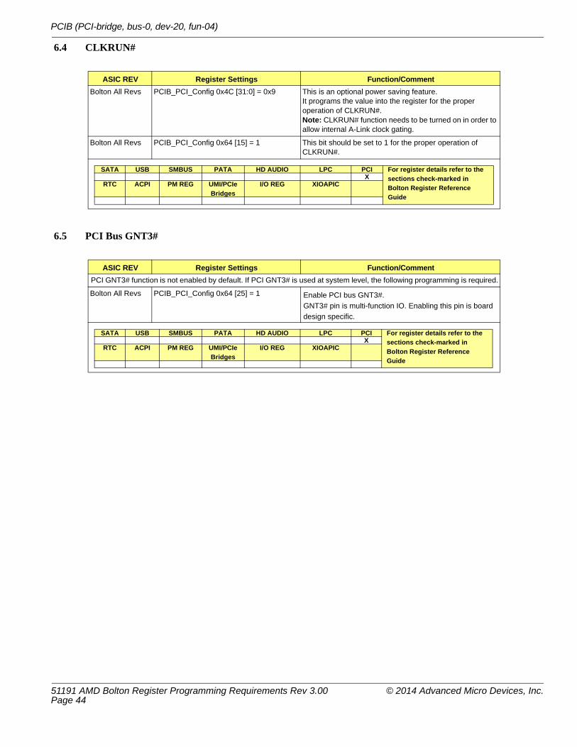
PCIB (PCI-bridge, bus-0, dev-20, fun-04)
6.4 CLKRUN#
6.5 PCI Bus GNT3#
ASIC REV Register Settings Function/CommentBolton All Revs PCIB_PCI_Config 0x4C [31:0] = 0x9 This is an optional power saving feature.
It programs the value into the register for the proper operation of CLKRUN#.Note: CLKRUN# function needs to be turned on in order to allow internal A-Link clock gating.
Bolton All Revs PCIB_PCI_Config 0x64 [15] = 1 This bit should be set to 1 for the proper operation of CLKRUN#.
ASIC REV Register Settings Function/CommentPCI GNT3# function is not enabled by default. If PCI GNT3# is used at system level, the following programming is required.
Bolton All Revs PCIB_PCI_Config 0x64 [25] = 1 Enable PCI bus GNT3#.GNT3# pin is multi-function IO. Enabling this pin is board design specific.
SATA USB SMBUS PATA HD AUDIO LPC PCI For register details refer to the sections check-marked in Bolton Register Reference Guide
XRTC ACPI PM REG UMI/PCIe
BridgesI/O REG XIOAPIC
SATA USB SMBUS PATA HD AUDIO LPC PCI For register details refer to the sections check-marked in Bolton Register Reference Guide
XRTC ACPI PM REG UMI/PCIe
BridgesI/O REG XIOAPIC
51191 AMD Bolton Register Programming Requirements Rev 3.00 © 2014 Advanced Micro Devices, Inc.Page 44

USB Controllers
7 USB Controllers
7.1 Device Mapping of OHCI, EHCI, and XHCI Controllers
7.1.1 Device List for Bolton
Device List Function/Comment
Bus-0, dev-18, fun-0 USB1, OHCI
Bus-0, dev-18, fun-2 USB1, EHCI
Bus-0, dev-19, fun-0 USB2, OHCI
Bus-0, dev-19, fun-2 USB2, EHCI
Bus-0, dev-16, fun-0 XHCI0
Bus-0, dev-16, fun-1 XHCI1
Bus-0, dev-20, fun-5 USB4, OHCI
© 2014 Advanced Micro Devices, Inc. 51191 AMD Bolton Register Programming Requirements Rev 3.00 Page 45

USB Controllers
7.2 Enabling USB Controllers
Programming of USB memory mapped registers is done by using the offset from:
• EHCI BAR address = EHCI_PCI_Config 0x10 [31:8]
• EHCI_EOR is the EHCI operation register = EHCI_BAR + 0x20
7.3 USB S4/S5 Wake-up or PHY Power-down Support
ASIC Rev Register Settings Function/CommentOHCI / EHCI controllers are enabled by default. If all the USB ports on any of these controllers are not used, then the controller can be disabled to minimize power consumption. Writing 0 to the responsible register will disable the controller.
Bolton All Revs PM_IO 0xEF [0] = 1 (default) Enable USB1 (bus-0, dev-18, fun-0) OHCI controller.
PM_IO 0xEF [1] = 1 (default) Enable USB1 (bus-0, dev-18, fun-2) EHCI controller.
PM_IO 0xEF [2] = 1 (default) Enable USB2 (bus-0, dev-19, fun-0) OHCI controller.
PM_IO 0xEF [3] = 1 (default) Enable USB2 (bus-0, dev-19, fun-2) EHCI controller.
PM_IO 0xEF [6] = 1 (default) Enable USB4 (bus-0, dev-20, fun-5) OHCI controller.
Bolton All Revs ACPI_USB3.0_Reg 0x00 [0] = 1 Enable XHCI0 controller (bus-0, dev-16, fun-0)
ACPI_USB3.0_Reg 0x00 [1] =1 Enable XHCI1 controller (bus-0, dev-16, fun-1)
ASIC Rev Register Settings Function/CommentBolton All Revs Option-1:
PM_IO 0xF0 [0] = 1
Option-2:PM_IO 0xF0 [0] = 0
Option 1:USB Wake from S5 not supported on the platformWhen the USB power rails USB PHY PLL, USB PHY core power and USB PHY DLL are connected to S0-S3 power, set the bit to 1 to disable the USB S4/S5 wakeup function
Option 2:USB Wake from S5 supported on the platformWhen the USB power rails USB PHY PLL, USB PHY core power and USB PHY DLL are connected to S5 power, set the bit to 0 to enable the USB S4/S5 wakeup function
SATA USB SMBUS PATA HD AUDIO LPC PCI For register details refer to the sections check-marked in Bolton Register Reference Guide
XRTC ACPI PM REG UMI/PCIe
BridgesI/O REG XIOAPIC
X
SATA USB SMBUS PATA HD AUDIO LPC PCI For register details refer to the sections check-marked in Bolton Register Reference Guide
RTC ACPI PM REG UMI/PCIe
BridgesI/O REG XIOAPIC
X
51191 AMD Bolton Register Programming Requirements Rev 3.00 © 2014 Advanced Micro Devices, Inc.Page 46
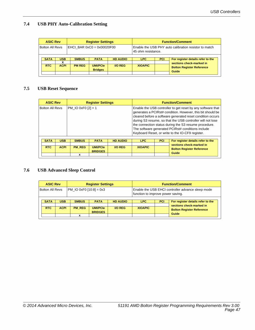
USB Controllers
7.4 USB PHY Auto-Calibration Setting
7.5 USB Reset Sequence
7.6 USB Advanced Sleep Control
ASIC Rev Register Settings Function/CommentBolton All Revs EHCI_BAR 0xC0 = 0x00020F00 Enable the USB PHY auto calibration resistor to match
45 ohm resistance.
ASIC Rev Register Settings Function/CommentBolton All Revs PM_IO 0xF0 [2] = 1 Enable the USB controller to get reset by any software that
generates a PCIRst# condition. However, this bit should be cleared before a software generated reset condition occurs during S3 resume, so that the USB controller will not lose the connection status during the S3 resume procedure.The software generated PCIRst# conditions include Keyboard Reset, or write to the IO-CF9 register.
ASIC Rev Register Settings Function/CommentBolton All Revs PM_IO 0xF0 [10:8] = 0x3 Enable the USB EHCI controller advance sleep mode
function to improve power saving.
SATA USB SMBUS PATA HD AUDIO LPC PCI For register details refer to the sections check-marked in Bolton Register Reference Guide
XRTC ACPI PM REG UMI/PCIe
BridgesI/O REG XIOAPIC
SATA USB SMBUS PATA HD AUDIO LPC PCI For register details refer to the sections check-marked in Bolton Register Reference Guide
RTC ACPI PM_REG UMI/PCIe
BRIDGESI/O REG XIOAPIC
x
SATA USB SMBUS PATA HD AUDIO LPC PCI For register details refer to the sections check-marked in Bolton Register Reference Guide
RTC ACPI PM_REG UMI/PCIe
BRIDGESI/O REG XIOAPIC
x
© 2014 Advanced Micro Devices, Inc. 51191 AMD Bolton Register Programming Requirements Rev 3.00 Page 47

USB Controllers
7.7 USB Delay UMI L1 State
7.8 USB 2.0 Ports Driving Strength
ASIC Rev Register Settings Function/CommentBolton All Revs ABCFG_Reg 0x90 [16] = 1
EHCI_PCI_Config 0x54 [0] = 1
Enable the feature in AB module to block UMI link from entering L1 state when USB controllers indicate active bus condition.
Set this bit to enable EHCI indication on bus activity.
With ABCFG_Reg x90 [16] set but EHCI bit not set, only OHCI activities will cause the L1 state blocking.
ASIC Rev Register Settings Function/CommentBolton All Revs Step 1a:
For any USB port that needs to be enabled, program the drive strength / slew rate values: EHCI_BAR 0xB4 [1:0] = {see note (b) }EHCI_BAR 0xB4 [2] = {see note (d)}EHCI_BAR 0xB4 [12] = 1 (“Vload”)EHCI_BAR 0xB4 [16:13] = {see note (c)}EHCI_BAR 0xB4 [9:7] = 3'b000Step 1bEHCI_BAR 0xB4 [12] = 0 ("Vloadb")Step 2:After programming the HSADJ drive strength / slew rate, set Vloadk to ‘1’ EHCI_BAR 0xB4 [12] = 1Step 3: EHCI_BAR 0xC4 [11:8] = 0x02EHCI_BAR 0XC0[15:8] = 0X0F
HSADJ to set the driving strength value.HSADJ to set the slew rate.
Select the Port# to load the HSADJ value to.
Set Vloadb to load the value for the selected port.
Set to '1' to lock PHY UTMI Control interface.
Adjust IREFADJ valueAdjust NewCalBus value
SATA USB SMBUS PATA HD AUDIO LPC PCI For register details refer to the sections check-marked in Bolton Register Reference Guide
xRTC ACPI PM REG UMI/PCIe
BridgesI/O REG XIOAPIC
x
51191 AMD Bolton Register Programming Requirements Rev 3.00 © 2014 Advanced Micro Devices, Inc.Page 48

USB Controllers
Notes: For Step 1: a) Depending on trace length and routing, adjust the driving strength to compensate for longer and shorter traces. The driving strength is on a per port basis. The port that needs to be adjusted must be selected by programming the Port Number field of the UTMI control register: i.e., bits [16:13] of EHCI_BAR offset B4h as shown in (b) below, where EHCI_BAR 0xB4 = EHCI_EOR 0x94 (UTMI control register).
b) EHCI_BAR 0xB4[1:0] (HSADJ)
c) EHCI_BAR 0xB4[16:13] (port number)
d) Set the slew rate: EHCI_BAR 0xB4[2] (HSADJ) For short traces (< 5"), set HSADJ [2] to 1. For traces = or > 5", leave the value at power up default setting of 0.
Bolton All Revs
HSADJ [1:0] 00 01 10 110% +7.5% +15% +22.5%
Trace Length Suggested Value(Short) < 5" HSADJ [1:0] = 00 (0%)(Medium) < 12" HSADJ [1:0] = 01 (+7.5%)(Long) > 12" HSADJ [1:0] = 10 (+15%)
EHCI Device 18 and Device 19Bits[16:13] 0000 0001 0010 0011 0100 0110 ~ 1111Port Number 0 1 2 3 4 reserved
Trace Length Required Value Comment(Short) < 5" HSADJ [2] = 1 Select slow slew rate(Medium) < 12" HSADJ [2] = 0 Select normal slew rate (power up default)(Long) > 12" HSADJ [2] = 0 Select normal slew rate (power up default)
SATA USB SMBUS PATA HD AUDIO LPC PCI For register details refer to the sections check-marked in Bolton Register Reference Guide
XRTC ACPI PM REG UMI/PCIe
BridgesI/O REG XIOAPIC
© 2014 Advanced Micro Devices, Inc. 51191 AMD Bolton Register Programming Requirements Rev 3.00 Page 49
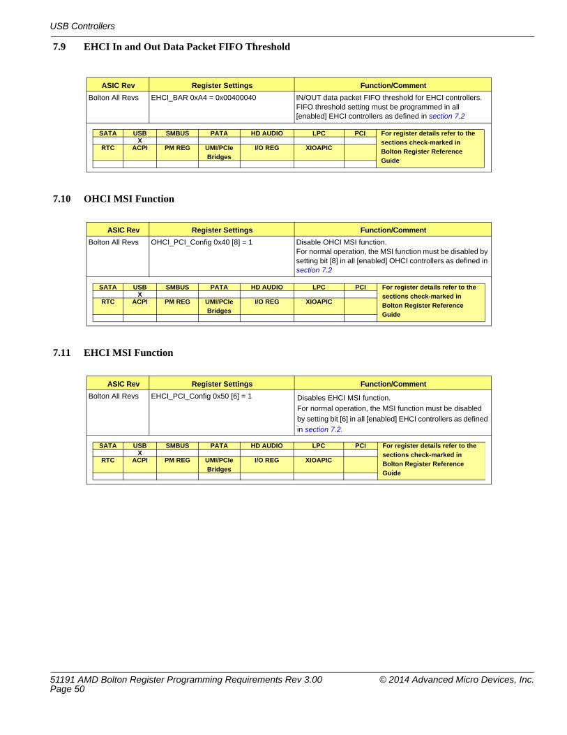
USB Controllers
7.9 EHCI In and Out Data Packet FIFO Threshold
7.10 OHCI MSI Function
7.11 EHCI MSI Function
ASIC Rev Register Settings Function/CommentBolton All Revs EHCI_BAR 0xA4 = 0x00400040 IN/OUT data packet FIFO threshold for EHCI controllers.
FIFO threshold setting must be programmed in all [enabled] EHCI controllers as defined in section 7.2
ASIC Rev Register Settings Function/CommentBolton All Revs OHCI_PCI_Config 0x40 [8] = 1 Disable OHCI MSI function.
For normal operation, the MSI function must be disabled by setting bit [8] in all [enabled] OHCI controllers as defined in section 7.2
ASIC Rev Register Settings Function/CommentBolton All Revs EHCI_PCI_Config 0x50 [6] = 1 Disables EHCI MSI function.
For normal operation, the MSI function must be disabled by setting bit [6] in all [enabled] EHCI controllers as defined in section 7.2.
SATA USB SMBUS PATA HD AUDIO LPC PCI For register details refer to the sections check-marked in Bolton Register Reference Guide
XRTC ACPI PM REG UMI/PCIe
BridgesI/O REG XIOAPIC
SATA USB SMBUS PATA HD AUDIO LPC PCI For register details refer to the sections check-marked in Bolton Register Reference Guide
XRTC ACPI PM REG UMI/PCIe
BridgesI/O REG XIOAPIC
SATA USB SMBUS PATA HD AUDIO LPC PCI For register details refer to the sections check-marked in Bolton Register Reference Guide
XRTC ACPI PM REG UMI/PCIe
BridgesI/O REG XIOAPIC
51191 AMD Bolton Register Programming Requirements Rev 3.00 © 2014 Advanced Micro Devices, Inc.Page 50

USB Controllers
7.12 USB SMI Handshake
7.13 EHCI Async Park Control
7.14 Extend InterPacket Gap
ASIC Rev Register Settings Function/CommentBolton All Revs OHCI_PCI_Config 0x50 [12] = 0 Enable SMI handshake between USB and ACPI.
The setting must be programmed in all [enabled] OHCI controllers as defined in section 7.2.
ASIC Rev Register Settings Function/CommentBolton All Revs EHCI_PCI_Config 0x50 [11:8] = 0x1
EHCI_PCI_Config 0x50 [15:12] = 0x1
EHCI_PCI_Config 0x50 [17] = 0x1
Enable advanced async park mode for IN transfers when async park mode is enabled by the host driver.
Enable advanced async park mode for OUT transfers when async park mode is enabled by the host driver.
Enable async park cache control.
The settings must be programmed in all [enabled] EHCI controllers as defined in section 7.2.
ASIC Rev Register Settings Function/CommentBolton All Revs EHCI_PCI_Config 0x50 [21] = 1 Enable extension of interpacket gap in PIE Idle state.
The setting must be programmed in all [enabled] EHCI controllers as defined in section 7.2.
SATA USB SMBUS PATA HD AUDIO LPC PCI For register details refer to the sections check-marked in Bolton Register Reference Guide
XRTC ACPI PM REG UMI/PCIe
BridgesI/O REG XIOAPIC
SATA USB SMBUS PATA HD AUDIO LPC PCI For register details refer to the sections check-marked in Bolton Register Reference Guide
XRTC ACPI PM REG UMI/PCIe
BridgesI/O REG XIOAPIC
SATA USB SMBUS PATA HD AUDIO LPC PCI For register details refer to the sections check-marked in Bolton Register Reference Guide
XRTC ACPI PM REG UMI/PCIe
BridgesI/O REG XIOAPIC
© 2014 Advanced Micro Devices, Inc. 51191 AMD Bolton Register Programming Requirements Rev 3.00 Page 51

USB Controllers
7.15 Empty List Mode
7.16 L1 Early Exit
7.17 EHCI PING Response Fix Enable
ASIC Rev Register Settings Function/CommentBolton All Revs EHCI_PCI_Config 0x54 [3] = 1 Enable empty list mode.
The setting must be programmed in all [enabled] EHCI controllers as defined in section 7.2.
ASIC Rev Register Settings Function/CommentBolton All Revs EHCI_PCI_Config 0x54 [6:5] = 0x3
EHCI_PCI_Config 0x54 [9:7] = 0x4
OHCI_PCI_Config 0x80 [0] = 1
Enable 'L1 Early Exit' functionality.
The setting must be programmed in all [enabled] EHCI controllers as defined in section 7.2.
The setting must be programmed in all [enabled] OHCI controllers as defined in section 7.2.
ASIC Rev Register Settings Function/CommentBolton All Revs EHCI_PCI_Config 0x54 [1] = 1 Enable PING Response fix.
Whenever a packet response like ACK, NAK is corrupted inside the PHY (due to bad SI), the MAC layer is supposed to compare the lower and upper nibble and discard it. But the logic was only looking at lower nibble to decide the type of response. The fix checks both upper nibble and lower nibble of the response byte to decide upon the response type.
The setting must be programmed in all [enabled] EHCI controllers as defined in section 7.2.
SATA USB SMBUS PATA HD AUDIO LPC PCI For register details refer to the sections check-marked in Bolton Register Reference Guide
XRTC ACPI PM REG UMI/PCIe
BridgesI/O REG XIOAPIC
SATA USB SMBUS PATA HD AUDIO LPC PCI For register details refer to the sections check-marked in Bolton Register Reference Guide
XRTC ACPI PM REG UMI/PCIe
BridgesI/O REG XIOAPIC
SATA USB SMBUS PATA HD AUDIO LPC PCI For register details refer to the sections check-marked in Bolton Register Reference Guide
XRTC ACPI PM REG UMI/PCIe
BridgesI/O REG XIOAPIC
51191 AMD Bolton Register Programming Requirements Rev 3.00 © 2014 Advanced Micro Devices, Inc.Page 52

USB Controllers
7.18 EHCI Async Stop Enhancement
7.19 Synchronize OHCI SOF
7.20 OHCI Periodic List Advance
ASIC Rev Register Settings Function/CommentBolton All Revs EHCI_PCI_Config 0x50 [29] = 1 Enable EHCI async stop enhancement.
Some software does not clear run/stop before clearing async-enable, and EHCI may take a long period of time to respond to the command. By enabling the enhancement, EHCI can respond to the command right after the completion of the current descriptor process.
The setting must be programmed in all [enabled] EHCI controllers as defined in section 7.2.
ASIC Rev Register Settings Function/CommentBolton All Revs OHCI_PCI_Config 0x52 [3] = 1 Enable OHCI SOF Synchronization.
The setting must be programmed in all [enabled] OHCI controllers as defined in section 7.2
ASIC Rev Register Settings Function/CommentBolton All Revs OHCI_PCI_Config 0x52 [4] = 1 Enable OHCI Periodic List Advance.
The setting must be programmed in all [enabled] OHCI controllers as defined in section 7.2.
SATA USB SMBUS PATA HD AUDIO LPC PCI For register details refer to the sections check-marked in Bolton Register Reference Guide
XRTC ACPI PM REG UMI/PCIe
BridgesI/O REG XIOAPIC
SATA USB SMBUS PATA HD AUDIO LPC PCI For register details refer to the sections check-marked in Bolton Register Reference Guide
XRTC ACPI PM REG UMI/PCIe
BridgesI/O REG XIOAPIC
SATA USB SMBUS PATA HD AUDIO LPC PCI For register details refer to the sections check-marked in Bolton Register Reference Guide
XRTC ACPI PM REG UMI/PCIe
BridgesI/O REG XIOAPIC
© 2014 Advanced Micro Devices, Inc. 51191 AMD Bolton Register Programming Requirements Rev 3.00 Page 53

USB Controllers
7.21 OHCI Arbiter Mode
7.22 USB 2.0 Global Clock Gating
ASIC Rev Register Settings Function/CommentBolton All Revs Step 1 (whenever the system resumes
from S3/S4/S5):a) Set ACPI PMIO 0xD3 [4] = 0b) Wait for < 1 micro secondc) Set ACPI PMIO 0xD3 [4] = 1
Step 2: a) OHCI_PCI_Config 0x80 [5:4] = 11bb) OHCI_PCI_Config 0x80 [8] = 1
Set OHCI Arbiter Mode.
The setting must be programmed in all [enabled] OHCI controllers as defined in section 7.2
ASIC Rev Register Settings Function/CommentBolton All Revs PM_IO 0xF0[12] = 1
PM_IO 0xFO[13] = 1EHCI_BAR 0xBC [12] = 1EHCI_BAR 0xBC [14] = 1
OHCI_PCI_Config 0x50 [0] = 0OHCI_PCI_Config 0x80 [7] = 1
Enable Global Clock Gating.
EHCI_BAR 0xBC[12] is 1 by default.The settings must be programmed for all [enabled] EHCI controllers as defined in section 7.2.
The settings must be programmed for all [enabled] OHCI controllers as defined in section 7.2
SATA USB SMBUS PATA HD AUDIO LPC PCI For register details refer to the sections check-marked in Bolton Register Reference Guide
XRTC ACPI PM REG UMI/PCIe
BridgesI/O REG XIOAPIC
SATA USB SMBUS PATA HD AUDIO LPC PCI For register details refer to the sections check-marked in Bolton Register Reference Guide
XRTC ACPI PM REG UMI/PCIe
BridgesI/O REG XIOAPIC
X
51191 AMD Bolton Register Programming Requirements Rev 3.00 © 2014 Advanced Micro Devices, Inc.Page 54

USB Controllers
7.23 USB 1.1 Full-Speed False CRC Errors Detected - CDR Logic Enhancement
7.24 Allow LS Devices to Wake up System from Sx states when EHCI Owns the Port
7.25 Fix for Long Read Latency Delays during Frame List Read by EHCI Controller Causing Malfunction
ASIC Rev Register Settings Function/CommentBolton All Revs OHCI_PCI_Config 0x80 [10] = 1 Set this bit to 1 to allow for proper USB CDR functionality
This setting must be programmed for all [enabled] OHCI controllers as defined in section 7.2.
ASIC Rev Register Settings Function/CommentBolton All Revs EHCI_PCI_Config 0x54 [4] = 1 Enable wake from S states for LS devices.
This setting must be programmed for all [enabled] EHCI controllers as defined in section 7.2.
ASIC Rev Register Settings Function/CommentBolton All Revs EHCI_PCI_Config 0x54 [15] = 1 When set to 1, the USB controller will properly process the
USB Periodic Frame List that has next QHeader pointer = null and T bit field set to 1.These settings must be programmed for all [enabled] EHCI controllers as defined in section 7.2.
SATA USB SMBUS PATA HD AUDIO LPC PCI For register details refer to the sections check-marked in Bolton Register Reference Guide
XRTC ACPI PM REG UMI/PCIe
BridgesI/O REG XIOAPIC
SATA USB SMBUS PATA HD AUDIO LPC PCI For register details refer to the sections check-marked in Bolton Register Reference Guide
XRTC ACPI PM REG UMI/PCIe
BridgesI/O REG XIOAPIC
SATA USB SMBUS PATA HD AUDIO LPC PCI For register details refer to the sections check-marked in Bolton Register Reference Guide
XRTC ACPI PM REG UMI/PCIe
BridgesI/O REG XIOAPIC
© 2014 Advanced Micro Devices, Inc. 51191 AMD Bolton Register Programming Requirements Rev 3.00 Page 55
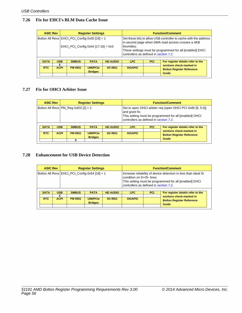
USB Controllers
7.26 Fix for EHCI's BLM Data Cache Issue
7.27 Fix for OHCI Arbiter Issue
7.28 Enhancement for USB Device Detection
ASIC Rev Register Settings Function/CommentBolton All Revs EHCI_PCI_Config 0x50 [19] = 1
EHCI_PCI_Config 0x54 [17:16] = 0x3
Set these bits to allow USB controller to cache with the address in second page when DMA read access crosses a 4KB boundary.These settings must be programmed for all [enabled] EHCI controllers as defined in section 7.2.
ASIC Rev Register Settings Function/CommentBolton All Revs PM_Reg 0xED [2] = 1 Set to open OHCI arbiter req (open OHCI PCI 0x80 [8, 5:4])
and grant fix.This setting must be programmed for all [enabled] OHCI controllers as defined in section 7.2.
ASIC Rev Register Settings Function/CommentBolton All Revs EHCI_PCI_Config 0x54 [18] = 1 Increase reliability of device detection in less than ideal SI
condition on D+/D- lines.This setting must be programmed for all [enabled] EHCI controllers as defined in section 7.2.
SATA USB SMBUS PATA HD AUDIO LPC PCI For register details refer to the sections check-marked in Bolton Register Reference Guide
XRTC ACPI PM REG UMI/PCIe
BridgesI/O REG XIOAPIC
SATA USB SMBUS PATA HD AUDIO LPC PCI For register details refer to the sections check-marked in Bolton Register Reference Guide
RTC ACPI PM REG UMI/PCIe
BridgesI/O REG XIOAPIC
X
SATA USB SMBUS PATA HD AUDIO LPC PCI For register details refer to the sections check-marked in Bolton Register Reference Guide
XRTC ACPI PM REG UMI/PCIe
BridgesI/O REG XIOAPIC
51191 AMD Bolton Register Programming Requirements Rev 3.00 © 2014 Advanced Micro Devices, Inc.Page 56

USB Controllers
7.29 Frame Babble Enhancement
7.30 EHCI Controller Data Babble to CRC Conversion Feature Disable
7.31 EHCI Controller Micro-Frame Counter Sync Enhancement
ASIC Rev Register Settings Function/CommentBolton All Revs EHCI_PCI_Config 0x54 [19] = 1 When this bit is set, the EHCI controller will disable only the
USB port that has detected the Babble error condition. All other ports will remain in their prior state.This setting must be programmed for all [enabled] EHCI controllers as defined in section 7.2.
ASIC Rev Register Settings Function/CommentBolton All Revs EHCI_BAR 0xB0 [5] = 1 By setting this bit, the data babble packets will not be retried
infinitely.The setting must be programmed for all [enabled] EHCI controllers as defined in section 7.2.
ASIC Rev Register Settings Function/CommentBolton All Revs EHCI_PCI_Config 0x54 [11] = 1 When this bit is set, the EHCI controller scheduler will function
correctly when the following condition is encountered: "only Periodic Schedule is enabled by the driver with the controller in the RUN state".This setting must be programmed for all [enabled] EHCI controllers as defined in section 7.2.
SATA USB SMBUS PATA HD AUDIO LPC PCI For register details refer to the sections check-marked in Bolton Register Reference Guide
XRTC ACPI PM REG UMI/PCIe
BridgesI/O REG XIOAPIC
SATA USB SMBUS PATA HD AUDIO LPC PCI For register details refer to the sections check-marked in Bolton Register Reference Guide
XRTC ACPI PM REG UMI/PCIe
BridgesI/O REG XIOAPIC
SATA USB SMBUS PATA HD AUDIO LPC PCI For register details refer to the sections check-marked in Bolton Register Reference Guide
XRTC ACPI PM REG UMI/PCIe
BridgesI/O REG XIOAPIC
© 2014 Advanced Micro Devices, Inc. 51191 AMD Bolton Register Programming Requirements Rev 3.00 Page 57

USB Controllers
7.32 OHCI Packet Buffer Threshold Settings
7.33 EHCI Frame List Processing Enhancement
7.34 Speed Field Enhancement
ASIC Rev Register Settings Function/CommentBolton All Revs OHCI_PCI_Config 0x52[7 :6] = 11b Set the optimal packet buffer threshold to accommodate longer
latency of downstream data. This setting must be programmed for all [enabled] OHCI controllers as defined in section 7.2.
ASIC Rev Register Settings Function/CommentBolton All Revs EHCI_PCI_Config 0x54[21] = 1 When this bit is set, the USB controller will check if there is
enough time left to fetch the next framelist within a uFrame.This setting must be programmed for all [enabled] EHCI controllers as defined in section 7.2.
ASIC Rev Register Settings Function/CommentBolton All Revs EHCI_PCI_Config 0x54[24] = 1 When the register bit is set, the USB controller will update the
S filed bit of start split transaction with the correct status of the link speed.This setting must be programmed for all [enabled] EHCI controllers as defined in section 7.2.
SATA USB SMBUS PATA HD AUDIO LPC PCI For register details refer to the sections check-marked in Bolton Register Reference Guide
XRTC ACPI PM REG UMI/PCIe
BridgesI/O REG XIOAPIC
SATA USB SMBUS PATA HD AUDIO LPC PCI For register details refer to the sections check-marked in Bolton Register Reference Guide
XRTC ACPI PM REG UMI/PCIe
BridgesI/O REG XIOAPIC
SATA USB SMBUS PATA HD AUDIO LPC PCI For register details refer to the sections check-marked in Bolton Register Reference Guide
XRTC ACPI PM REG UMI/PCIe
BridgesI/O REG XIOAPIC
51191 AMD Bolton Register Programming Requirements Rev 3.00 © 2014 Advanced Micro Devices, Inc.Page 58

USB Controllers
7.35 Save Status of EHCI/OHCI Connect/Disconnect in S3
7.36 ISO Device CRC False Error Detection
7.37 EHCI Data Cache Enhancement
ASIC Rev Register Settings Function/CommentBolton All Revs PM_IO 0xF4 [0] = 1 When this bit is set, the USB EHCI/OHCI controller will save
the status of any connect/disconnect transactions while the controller is in S3 sleep state. On subsequent wake event, the controller will update the driver with the pending status changes so the drive is in sync with the device status changes while the system was in sleep state.
ASIC Rev Register Settings Function/CommentFor all USB ports that are supported within each EHCI controller, the following sequence should be applied.
Bolton All Revs Step 1 EHCI_BAR 0xB4[16:13] = Port number EHCI_BAR 0xB4[9:7] = 'b111 EHCI_BAR 0xB4 [2:0] = 'b101 EHCI_BAR 0xB4[12] = 'b1Step 2 EHCI_BAR 0xB4[12] = 'b0Step 3 EHCI_BAR 0xB4[12] = 'b1
Enter Port # value from table in note (a) belowSelect group #
Note (a):
ASIC Rev Register Settings Function/CommentBolton All Revs EHCI_PCI_Config 0x54[20] = 1 Set this bit to 1 to enable data cache logic enhancement. It
prevents the controller from using cached data on page boundary and flushes prefetch cache on completion of the transaction.This setting must be programmed for all [enabled] EHCI controllers as defined in section 7.2.
SATA USB SMBUS PATA HD AUDIO LPC PCI For register details refer to the sections check-marked in Bolton Register Reference Guide
RTC ACPI PM REG UMI/PCIe
BridgesI/O REG XIOAPIC
X
EHCI Device 18 and 19Port Number 0000 0001 0010 0011 0100 0101~1111
0 1 2 3 4 Reserved
SATA USB SMBUS PATA HD AUDIO LPC PCI For register details refer to the sections check-marked in Bolton Register Reference Guide
XRTC ACPI PM REG UMI/PCIe
BridgesI/O REG XIOAPIC
SATA USB SMBUS PATA HD AUDIO LPC PCI For register details refer to the sections check-marked in Bolton Register Reference Guide
XRTC ACPI PM REG UMI/PCIe
BridgesI/O REG XIOAPIC
© 2014 Advanced Micro Devices, Inc. 51191 AMD Bolton Register Programming Requirements Rev 3.00 Page 59

USB Controllers
7.38 Unexpected Linux Driver TD Setup Causing EHCI to Hang
7.39 Reset Connect Timer when Disconnecting
7.40 EHCI_PME Should Be Gated by PME Enable Bit
7.41 EHCI Required to Support De-Linking Async Active QH
ASIC Rev Register Settings Function/CommentBolton All Revs EHCI_PCI_Config 0x54[22] = 1 Set this bit to 1 to allow the controller to handle halt bit set with
the controller in active run state.This setting must be programmed for all [enabled] EHCI controllers as defined in section 7.2.
ASIC Rev Register Settings Function/CommentBolton All Revs EHCI_PCI_Config 0x54[25] = 1 Set this bit to 1 to enable logic enhancement for the timer to
handle Connect detection and Disconnect detection state changes within one clock cycle. This setting must be programmed for all [enabled] EHCI controllers as defined in section 7.2.
ASIC Rev Register Settings Function/CommentBolton All Revs EHCI_PCI_Config 0x54[27] = 1
EHCI_PCI_Config 0x50[0] = 1Set these registers to '1' to enable enhancement for internal PME conditions to be masked off with PME enable.These settings must be programmed for all [enabled] EHCI controllers as defined in section 7.2.
ASIC Rev Register Settings Function/CommentBolton All Revs EHCI_PCI_Config 0x54[28] = 1 Set this bit to 1 to allow EHCI controller detect if the cached
Async QH is de-linked by software, and terminate the workload of this cached QH.This setting must be programmed for all [enabled] EHCI controllers as defined in section 7.2.
SATA USB SMBUS PATA HD AUDIO LPC PCI For register details refer to the sections check-marked in Bolton Register Reference Guide
XRTC ACPI PM REG UMI/PCIe
BridgesI/O REG XIOAPIC
SATA USB SMBUS PATA HD AUDIO LPC PCI For register details refer to the sections check-marked in Bolton Register Reference Guide
XRTC ACPI PM REG UMI/PCIe
BridgesI/O REG XIOAPIC
SATA USB SMBUS PATA HD AUDIO LPC PCI For register details refer to the sections check-marked in Bolton Register Reference Guide
XRTC ACPI PM REG UMI/PCIe
BridgesI/O REG XIOAPIC
SATA USB SMBUS PATA HD AUDIO LPC PCI For register details refer to the sections check-marked in Bolton Register Reference Guide
XRTC ACPI PM REG UMI/PCIe
BridgesI/O REG XIOAPIC
51191 AMD Bolton Register Programming Requirements Rev 3.00 © 2014 Advanced Micro Devices, Inc.Page 60
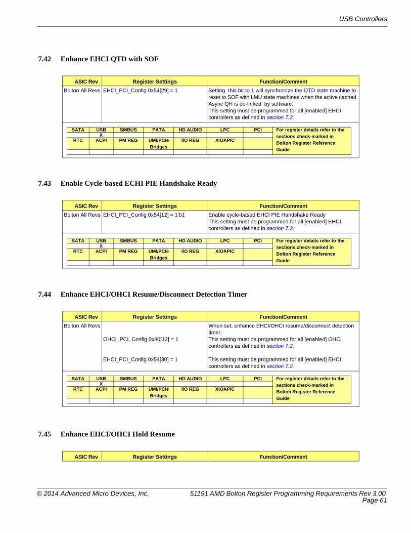
USB Controllers
7.42 Enhance EHCI QTD with SOF
7.43 Enable Cycle-based ECHI PIE Handshake Ready
7.44 Enhance EHCI/OHCI Resume/Disconnect Detection Timer
7.45 Enhance EHCI/OHCI Hold Resume
ASIC Rev Register Settings Function/CommentBolton All Revs EHCI_PCI_Config 0x54[29] = 1 Setting this bit to 1 will synchronize the QTD state machine to
reset to SOF with LMU state machines when the active cached Async QH is de-linked by software.This setting must be programmed for all [enabled] EHCI controllers as defined in section 7.2.
ASIC Rev Register Settings Function/CommentBolton All Revs EHCI_PCI_Config 0x54[12] = 1'b1 Enable cycle-based EHCI PIE Handshake Ready
This setting must be programmed for all [enabled] EHCI controllers as defined in section 7.2.
ASIC Rev Register Settings Function/CommentBolton All Revs
OHCI_PCI_Config 0x80[12] = 1
EHCI_PCI_Config 0x54[30] = 1
When set, enhance EHCI/OHCI resume/disconnect detection timer.This setting must be programmed for all [enabled] OHCI controllers as defined in section 7.2.
This setting must be programmed for all [enabled] EHCI controllers as defined in section 7.2.
ASIC Rev Register Settings Function/Comment
SATA USB SMBUS PATA HD AUDIO LPC PCI For register details refer to the sections check-marked in Bolton Register Reference Guide
XRTC ACPI PM REG UMI/PCIe
BridgesI/O REG XIOAPIC
SATA USB SMBUS PATA HD AUDIO LPC PCI For register details refer to the sections check-marked in Bolton Register Reference Guide
XRTC ACPI PM REG UMI/PCIe
BridgesI/O REG XIOAPIC
SATA USB SMBUS PATA HD AUDIO LPC PCI For register details refer to the sections check-marked in Bolton Register Reference Guide
XRTC ACPI PM REG UMI/PCIe
BridgesI/O REG XIOAPIC
© 2014 Advanced Micro Devices, Inc. 51191 AMD Bolton Register Programming Requirements Rev 3.00 Page 61
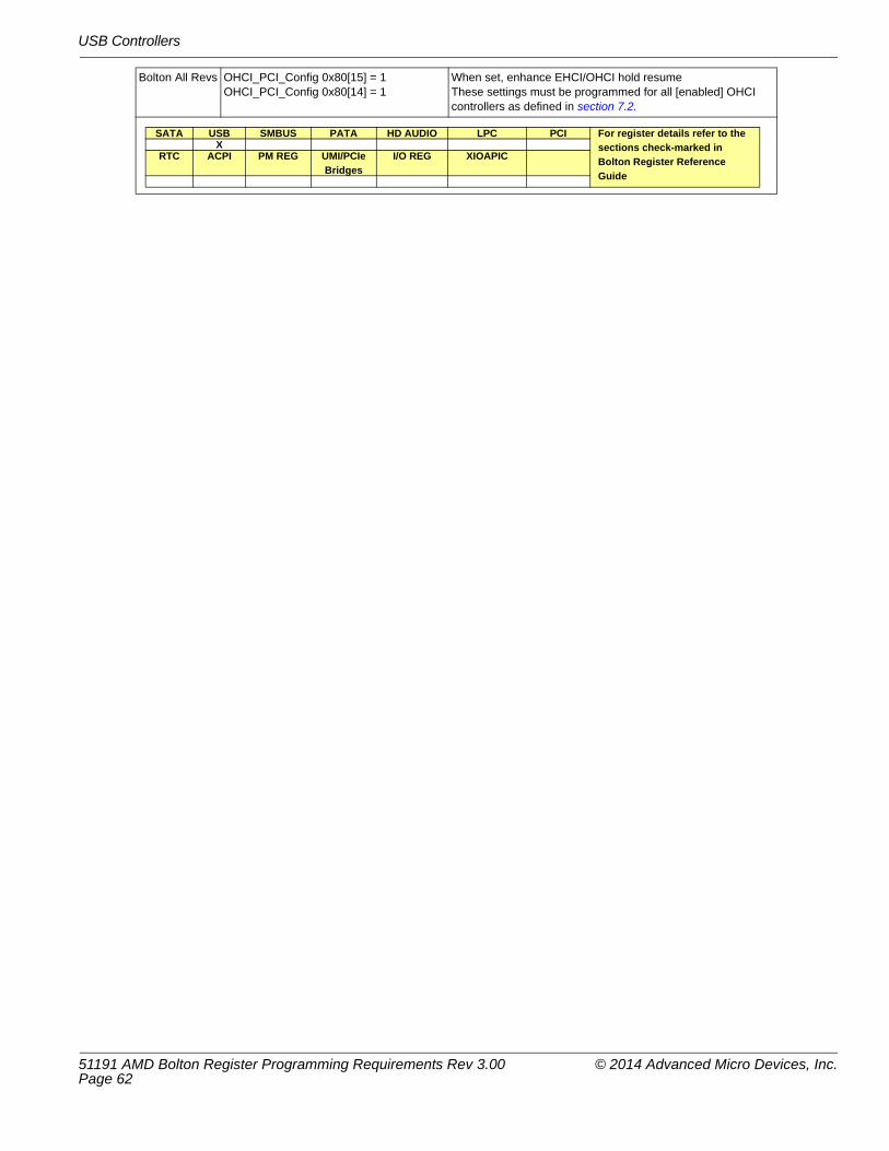
USB Controllers
Bolton All Revs OHCI_PCI_Config 0x80[15] = 1OHCI_PCI_Config 0x80[14] = 1
When set, enhance EHCI/OHCI hold resumeThese settings must be programmed for all [enabled] OHCI controllers as defined in section 7.2.
SATA USB SMBUS PATA HD AUDIO LPC PCI For register details refer to the sections check-marked in Bolton Register Reference Guide
XRTC ACPI PM REG UMI/PCIe
BridgesI/O REG XIOAPIC
51191 AMD Bolton Register Programming Requirements Rev 3.00 © 2014 Advanced Micro Devices, Inc.Page 62

USB xHCI Controllers
8 USB xHCI Controllers Note: Not all Bolton variants support XHCI controller. Refer to individual data books for details.
8.1 SMI Enable
8.2 BLM Message Enable
8.3 USB 3.0 (SuperSpeed) PHY Configuration
8.4 USB 3.0 Reference Clock
ASIC Rev Register Settings Function/CommentBolton All Revs ACPI_USB3.0_Reg 0x00 [21] = 1 Enable xHCI SMI.
bus-0, dev-16, fun-0 / bus-0, dev-16, fun-1
ASIC Rev Register Settings Function/CommentBolton All Revs PCI_IND_Reg 0x00 [26:24] = 0x7 Enable Interrupt, LTR, Error Messages.
bus-0, dev-16, fun-0 / bus-0, dev-16, fun-1
Note: This register setting needs to be restored after all power state resumes.
ASIC Rev Register Settings Function/CommentBolton All Revs ACPI_USB3.0_Reg 0x90 [19:0] = 0xAAAAA Set certain parameters to tune USB 3.0 PHY.
Note: ACPI_USB3.0_Reg register settings must be performed before setting U3_Core_Reset and U3P_Phy_Reset to 0. PCI_IND_Reg register settings need to be applied right after setting U3_Core_Reset to 0.
ASIC Rev Register Settings Function/CommentBolton All Revs MISC_REG 0x40 [4] = 0 Enable spread-spectrum reference clock.
SATA USB SMBUS PATA HD AUDIO LPC PCI For register details refer to the sections check-marked in Bolton Register Reference Guide
XRTC ACPI PM REG UMI/PCIe
BridgesI/O REG XIOAPIC
SATA USB SMBUS PATA HD AUDIO LPC PCI For register details refer to the sections check-marked in Bolton Register Reference Guide
XRTC ACPI PM REG UMI/PCIe
BridgesI/O REG XIOAPIC
X
SATA USB SMBUS PATA HD AUDIO LPC PCI For register details refer to the sections check-marked in Bolton Register Reference Guide
XRTC ACPI PM REG UMI/PCIe
BridgesI/O REG XIOAPIC
X
© 2014 Advanced Micro Devices, Inc. 51191 AMD Bolton Register Programming Requirements Rev 3.00 Page 63
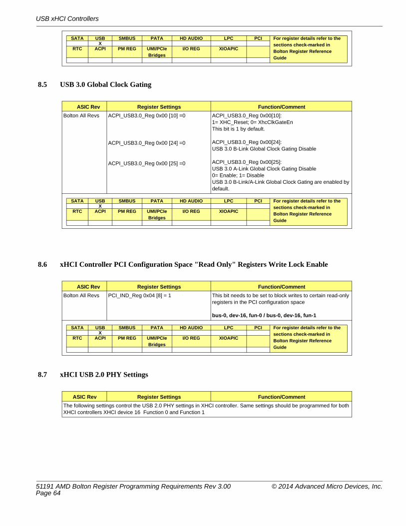
USB xHCI Controllers
8.5 USB 3.0 Global Clock Gating
8.6 xHCI Controller PCI Configuration Space "Read Only" Registers Write Lock Enable
8.7 xHCI USB 2.0 PHY Settings
ASIC Rev Register Settings Function/CommentBolton All Revs ACPI_USB3.0_Reg 0x00 [10] =0
ACPI_USB3.0_Reg 0x00 [24] =0
ACPI_USB3.0_Reg 0x00 [25] =0
ACPI_USB3.0_Reg 0x00[10]:1= XHC_Reset; 0= XhcClkGateEnThis bit is 1 by default.
ACPI_USB3.0_Reg 0x00[24]: USB 3.0 B-Link Global Clock Gating Disable
ACPI_USB3.0_Reg 0x00[25]: USB 3.0 A-Link Global Clock Gating Disable0= Enable; 1= DisableUSB 3.0 B-Link/A-Link Global Clock Gating are enabled by default.
ASIC Rev Register Settings Function/CommentBolton All Revs PCI_IND_Reg 0x04 [8] = 1 This bit needs to be set to block writes to certain read-only
registers in the PCI configuration space
bus-0, dev-16, fun-0 / bus-0, dev-16, fun-1
ASIC Rev Register Settings Function/CommentThe following settings control the USB 2.0 PHY settings in XHCI controller. Same settings should be programmed for both XHCI controllers XHCI device 16 Function 0 and Function 1
SATA USB SMBUS PATA HD AUDIO LPC PCI For register details refer to the sections check-marked in Bolton Register Reference Guide
XRTC ACPI PM REG UMI/PCIe
BridgesI/O REG XIOAPIC
SATA USB SMBUS PATA HD AUDIO LPC PCI For register details refer to the sections check-marked in Bolton Register Reference Guide
XRTC ACPI PM REG UMI/PCIe
BridgesI/O REG XIOAPIC
SATA USB SMBUS PATA HD AUDIO LPC PCI For register details refer to the sections check-marked in Bolton Register Reference Guide
XRTC ACPI PM REG UMI/PCIe
BridgesI/O REG XIOAPIC
51191 AMD Bolton Register Programming Requirements Rev 3.00 © 2014 Advanced Micro Devices, Inc.Page 64

USB xHCI Controllers
Bolton All Revs Step 1:For any USB port that needs to be enabled, program the drive strength / slew rate values: IND60_Reg: 00h [1:0] = {see note (b) }IND60_Reg: 00h [2] = {see note (d)}IND60_Reg: 00h [12] = 1 (“Vloadb”)IND60_Reg: 00h [16:13] = { see note (c)}Step 2:Set VloadB to '0' to load the value for the selected port:IND60_Reg: 00h [12] = 0Step 3:After programming the HSADJ drive strength / slew rate, set Vloadb to ‘1’ IND60_Reg: 00h [12] = 1
HSADJ to set the driving strength value.HSADJ to set the slew rate.Set Vloadb to load the value for the selected port.Select the Port# to load the HSADJ value to.
Set VloadB to load the value for the selected port
Set to '1' to lock PHY UTMI Control interface.
Note: These register settings need to be restored after all power state resumes.
Notes: For Step 1 (All Revs): a) Depending on trace length and routing, adjust the driving strength to compensate for longer and shorter traces. The driving strength is on a per port basis. The port that needs to be adjusted must be selected by programming the Port Number field of the UTMI control register. UTMI Control register can be accessed from Indirect PCI index and Indirect PCI data index/data registers at PCI config space register offsets 48h/4Ch.
b) IND60_Reg: 00h [1:0] (HSADJ)
c) IND60_Reg: 00h [16:13] (Port Number)
d) Set the slew rate: IND60_Reg: 00h [2] (HSADJ)
Bolton All Revs
HSADJ [1:0] 00 01 10 110% +7.5% +15% +22.5%
Trace Length Required Value(Short) < 5" HSADJ [1:0] = 00 (0%)(Medium) </ = 10" HSADJ [1:0] = 01 = (+ 7.5%)
xHCI Device 16 Functio 0 and Function 1Bits [16:13] 0000 0001 0010 ~ 1111Port Number 0 1 reserved
Trace Length Required Value Comment(Short) < 5" HSADJ [2] = 1 Select slow slew rate(Medium) </ = 10" HSADJ [2] = 0 Select normal slew rate (power up default)
SATA USB SMBUS PATA HD AUDIO LPC PCI For register details refer to the sections check-marked in Bolton Register Reference Guide
XRTC ACPI PM REG UMI/PCIe
BridgesI/O REG XIOAPIC
© 2014 Advanced Micro Devices, Inc. 51191 AMD Bolton Register Programming Requirements Rev 3.00 Page 65

USB xHCI Controllers
8.8 Allow Access to EHCI/OHCI Register through JTAG
8.9 USB PHY Suspend State Enhancement
8.10 UMI Lane Configuration Information for xHCI Firmware to Calculate the Bandwidth for USB 3.0 ISOC Devices
8.11 Fix for Incorrect Gated Signals in xhc_to_s5
ASIC Rev Register Settings Function/CommentBolton All Revs PM_IO 0xF0 [17] = 1 Allow run time switching of JTAG control between xHCI
and EHCI/OHCI controllers.
ASIC Rev Register Settings Function/CommentBolton All Revs PM_IO 0xF0 [14] = 1 Set the suspend signal going to USB 2.0 PHY to active
state when no device is connected.
ASIC Rev Register Settings Function/CommentBolton All Revs Step 1: Read AXCFG 0x68 register
Step 2: If (bits[19:16] = 2 ) or (bit[19:16] = 1 and bits [25:20] > 1) then set ACPI_USB3.0_REG 0x20 [25:24] = 0x1
Settings to let the firmware know the available bandwidth on the UMI link which is used for calculating the bandwidth allocation for USB 3.0 ISOC devices.
ASIC Rev Register Settings Function/CommentBolton All Revs PM_Reg 0xF0 [16] = 1 Set this bit to 1 to allow xHCI related signals to be gated
when the xHCI controller is in S3/S5 states.
SATA USB SMBUS PATA HD AUDIO LPC PCI For register details refer to the sections check-marked in Bolton Register Reference Guide
RTC ACPI PM REG UMI/PCIe
BridgesI/O REG XIOAPIC
X
SATA USB SMBUS PATA HD AUDIO LPC PCI For register details refer to the sections check-marked in Bolton Register Reference Guide
RTC ACPI PM REG UMI/PCIe
BridgesI/O REG XIOAPIC
X
SATA USB SMBUS PATA HD AUDIO LPC PCI For register details refer to the sections check-marked in Bolton Register Reference Guide
RTC ACPI PM REG UMI/PCIe
BridgesI/O REG XIOAPIC
X
SATA USB SMBUS PATA HD AUDIO LPC PCI For register details refer to the sections check-marked in Bolton Register Reference Guide
RTC ACPI PM REG UMI/PCIe
BridgesI/O REG XIOAPIC
X
51191 AMD Bolton Register Programming Requirements Rev 3.00 © 2014 Advanced Micro Devices, Inc.Page 66

USB xHCI Controllers
8.12 xHCI USB 2.0 PHY Clock Gating and Rise Time Configuration
8.13 xHCI Clear Pending PME on Sx Entry
ASIC Rev Register Settings Function/CommentBolton All Revs Step1:
PCI IND60_Reg00h[16:13] = port number 0000: port0 0001: port1
PCI IND60_Reg00h[12] = 1;PCI IND60_Reg00h[9:7] = 'b011PCI IND60_Reg00h[6:0] = 'b1000100;
Step 2:Read IND60_Reg: 00h [17] to ensure it isset to 0
Step 3:PCI IND60_Reg00h[12] = 0;
Step 4:Read IND60_Reg: 00h [17] to ensure it isset to 0
Step 5:PCI IND60_Reg00h[12] = 1;
Step 6:ACPI_USB3.0_REG 0xB4[23] = 1'b1
Configure USB2 PHY Clock Gating and Low-Speed Rise Time.
Programming steps 1-5 should be done for both controllers:bus-0, dev-16, fun-0 and bus-0, dev-16, fun-1
Program for all of the ports in each controller as set by IND60_Reg: 00h [16:13] = port #
ASIC Rev Register Settings Function/CommentBolton All Revs xHCI_PCI_ Config 0x54 [15] = 1
(on condition described in the comment column)
Clear XHCI PME status on bus-0, dev-16, fun-0 / bus-0, dev-16, fun-1
On entry into S3/S4 check if XHCI PME Status bit is set && ACPI Gevent Status bit is cleared, then clear XHCI PME Status bit. See Note below.
Note: If during an S3/S4 entry (with Wake from Sx state enabled), the XHCI controller receives a Wake event before the system shutdown into Sx state is completed, the XHCI controller PME status bit may remain set when the system enters into Sx state. This will prevent subsequent wake events from being propagated to the ACPI controller. The above setting will clear the pending PME that is not expected to be processed as the system enters into Sx state.
SATA USB SMBUS PATA HD AUDIO LPC PCI For register details refer to the sections check-marked in Bolton Register Reference Guide
XRTC ACPI PM REG UMI/PCIe
BridgesI/O REG XIOAPIC
SATA USB SMBUS PATA HD AUDIO LPC PCI For register details refer to the sections check-marked in Bolton Register Reference Guide
XRTC ACPI PM REG UMI/PCIe
BridgesI/O REG XIOAPIC
X
© 2014 Advanced Micro Devices, Inc. 51191 AMD Bolton Register Programming Requirements Rev 3.00 Page 67

USB xHCI Controllers
8.14 D3Cold ccu Sequencing Enhancement
ASIC Rev Register Settings Function/CommentBolton All Revs ACPI_USB3.0_REG 0x10[11] = 1 Enable design modifications to D3Cold ccu sequencing
SATA USB SMBUS PATA HD AUDIO LPC PCI For register details refer to the sections check-marked in Bolton Register Reference Guide
XRTC ACPI PM REG UMI/PCIe
BridgesI/O REG XIOAPIC
X
51191 AMD Bolton Register Programming Requirements Rev 3.00 © 2014 Advanced Micro Devices, Inc.Page 68

USB xHCI Controllers
8.15 Set HCI Version to 1.0
8.16 xHCI 1.0 Sub-Features Supported
ASIC Rev Register Settings Function/CommentBolton All Revs ACPI_USB3.0_REG 0x30[15] = 1 Set the xHCI Host Controller Interface Version Number
(HCIVERSION) to 1.0
ASIC Rev Register Settings Feature Function/Comment
Enabled DisabledBolton All Revs
ACPI_USB3.0_REG 0x30[1] = 1 x Block Event Interrupt Flag; [BEI]
ACPI_USB3.0_REG 0x30[2] = 1 x Force Stopped Event (FSE)
ACPI_USB3.0_REG 0x30[3] = 1 x Software LPM
ACPI_USB3.0_REG 0x30[6] = 1 x SKIP TRB IOC Event
ACPI_USB3.0_REG 0x30[7] = 1 x Remove Secondary Bandwidth Domain Reporting Capability.
ACPI_USB3.0_REG 0x30[8] = 1 x Cold Attach
ACPI_USB3.0_REG 0x30[9] = 1 x EPState Update
ACPI_USB3.0_REG 0x30[10] = 1 x Report Event during SKIP on Missed Service Error
ACPI_USB3.0_REG 0x30[11] = 1 x Soft Retry
ACPI_USB3.0_REG 0x30[12] = 1 x U3 Exit
ACPI_USB3.0_REG 0x30[13] = 1 x USB 3.0 Link Command
ACPI_USB3.0_REG 0x30[14] = 1 x MSE FrameID invalid
ACPI_USB3.0_REG 0x30[16] = 1 x Port Test Mode
ACPI_USB3.0_REG 0x30[24] = 1 x SKIP_TRB_IOC_EVT_LEN_MODE
ACPI_USB3.0_REG 0x40[0] = 1 x Miscellaneous Design Improvement
ACPI_USB3.0_Ind_REG 0x100[0] = 1 x XHC Debug Capability
SATA USB SMBUS PATA HD AUDIO LPC PCI For register details refer to the sections check-marked in Bolton Register Reference Guide
XRTC ACPI PM REG UMI/PCIe
BridgesI/O REG XIOAPIC
X
SATA USB SMBUS PATA HD AUDIO LPC PCI For register details refer to the sections check-marked in Bolton Register Reference Guide
XRTC ACPI PM REG UMI/PCIe
BridgesI/O REG XIOAPIC
X
© 2014 Advanced Micro Devices, Inc. 51191 AMD Bolton Register Programming Requirements Rev 3.00 Page 69
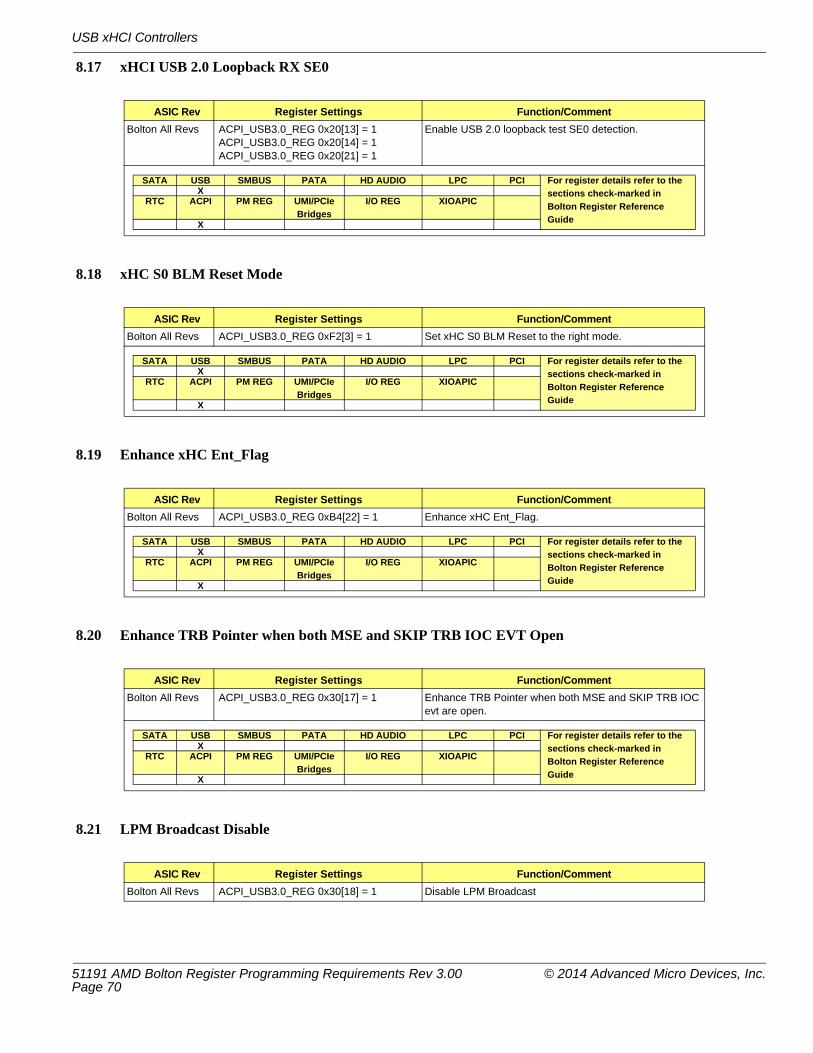
USB xHCI Controllers
8.17 xHCI USB 2.0 Loopback RX SE0
8.18 xHC S0 BLM Reset Mode
8.19 Enhance xHC Ent_Flag
8.20 Enhance TRB Pointer when both MSE and SKIP TRB IOC EVT Open
8.21 LPM Broadcast Disable
ASIC Rev Register Settings Function/CommentBolton All Revs ACPI_USB3.0_REG 0x20[13] = 1
ACPI_USB3.0_REG 0x20[14] = 1ACPI_USB3.0_REG 0x20[21] = 1
Enable USB 2.0 loopback test SE0 detection.
ASIC Rev Register Settings Function/CommentBolton All Revs ACPI_USB3.0_REG 0xF2[3] = 1 Set xHC S0 BLM Reset to the right mode.
ASIC Rev Register Settings Function/CommentBolton All Revs ACPI_USB3.0_REG 0xB4[22] = 1 Enhance xHC Ent_Flag.
ASIC Rev Register Settings Function/CommentBolton All Revs ACPI_USB3.0_REG 0x30[17] = 1 Enhance TRB Pointer when both MSE and SKIP TRB IOC
evt are open.
ASIC Rev Register Settings Function/CommentBolton All Revs ACPI_USB3.0_REG 0x30[18] = 1 Disable LPM Broadcast
SATA USB SMBUS PATA HD AUDIO LPC PCI For register details refer to the sections check-marked in Bolton Register Reference Guide
XRTC ACPI PM REG UMI/PCIe
BridgesI/O REG XIOAPIC
X
SATA USB SMBUS PATA HD AUDIO LPC PCI For register details refer to the sections check-marked in Bolton Register Reference Guide
XRTC ACPI PM REG UMI/PCIe
BridgesI/O REG XIOAPIC
X
SATA USB SMBUS PATA HD AUDIO LPC PCI For register details refer to the sections check-marked in Bolton Register Reference Guide
XRTC ACPI PM REG UMI/PCIe
BridgesI/O REG XIOAPIC
X
SATA USB SMBUS PATA HD AUDIO LPC PCI For register details refer to the sections check-marked in Bolton Register Reference Guide
XRTC ACPI PM REG UMI/PCIe
BridgesI/O REG XIOAPIC
X
51191 AMD Bolton Register Programming Requirements Rev 3.00 © 2014 Advanced Micro Devices, Inc.Page 70

USB xHCI Controllers
8.22 Enhance xHC FS/LS Connect
8.23 Enhance xHC ISOCH td_cmp
8.24 LPM Clock 5us Select
8.25 Enhance DPP ERR as XactErr
ASIC Rev Register Settings Function/CommentBolton All Revs ACPI_USB3.0_REG 0xB4[24] = 1 Enhance xHC FS/LS Connect.
ASIC Rev Register Settings Function/CommentBolton All Revs ACPI_USB3.0_REG 0xB4[25] = 1 Enhance xHC ISOCH td_cmp.
ASIC Rev Register Settings Function/CommentBolton All Revs ACPI_USB3.0_REG 0x24[8] = 1 Enhance LPM Clock 5us.
ASIC Rev Register Settings Function/CommentBolton All Revs ACPI_USB3.0_REG 0x24[9] = 1 Enhance DPP ERR as XactErr.
SATA USB SMBUS PATA HD AUDIO LPC PCI For register details refer to the sections check-marked in Bolton Register Reference Guide
XRTC ACPI PM REG UMI/PCIe
BridgesI/O REG XIOAPIC
X
SATA USB SMBUS PATA HD AUDIO LPC PCI For register details refer to the sections check-marked in Bolton Register Reference Guide
XRTC ACPI PM REG UMI/PCIe
BridgesI/O REG XIOAPIC
X
SATA USB SMBUS PATA HD AUDIO LPC PCI For register details refer to the sections check-marked in Bolton Register Reference Guide
XRTC ACPI PM REG UMI/PCIe
BridgesI/O REG XIOAPIC
X
SATA USB SMBUS PATA HD AUDIO LPC PCI For register details refer to the sections check-marked in Bolton Register Reference Guide
XRTC ACPI PM REG UMI/PCIe
BridgesI/O REG XIOAPIC
X
SATA USB SMBUS PATA HD AUDIO LPC PCI For register details refer to the sections check-marked in Bolton Register Reference Guide
XRTC ACPI PM REG UMI/PCIe
BridgesI/O REG XIOAPIC
X
© 2014 Advanced Micro Devices, Inc. 51191 AMD Bolton Register Programming Requirements Rev 3.00 Page 71

USB xHCI Controllers
8.26 Enhance U2IF PME Enable
8.27 Enhance U2IF S3 Disconnect Detection
8.28 Stream Error Handling
8.29 FLA Deassert
8.30 LPM Ctrl Improvement
ASIC Rev Register Settings Function/CommentBolton All Revs ACPI_USB3.0_REG 0x24[10] = 1 Enhance U2IF PME Enable.
ASIC Rev Register Settings Function/CommentBolton All Revs ACPI_USB3.0_REG 0x24[12] = 1 Enhance U2IF S3 Disconnect detection.
ASIC Rev Register Settings Function/CommentBolton All Revs ACPI_USB3.0_REG 0x30[20] = 1
ACPI_USB3.0_REG 0x30[21] = 1ACPI_USB3.0_REG 0x30[22] = 1
Enhance Stream Error Handling.
ASIC Rev Register Settings Function/CommentBolton All Revs ACPI_USB3.0_REG 0x30[23] = 1 Enable FLA Deassert.
ASIC Rev Register Settings Function/CommentBolton All Revs ACPI_USB3.0_REG 0x30[27] = 1 Enable LPM Ctrl improvement.
SATA USB SMBUS PATA HD AUDIO LPC PCI For register details refer to the sections check-marked in Bolton Register Reference Guide
XRTC ACPI PM REG UMI/PCIe
BridgesI/O REG XIOAPIC
X
SATA USB SMBUS PATA HD AUDIO LPC PCI For register details refer to the sections check-marked in Bolton Register Reference Guide
XRTC ACPI PM REG UMI/PCIe
BridgesI/O REG XIOAPIC
X
SATA USB SMBUS PATA HD AUDIO LPC PCI For register details refer to the sections check-marked in Bolton Register Reference Guide
XRTC ACPI PM REG UMI/PCIe
BridgesI/O REG XIOAPIC
X
SATA USB SMBUS PATA HD AUDIO LPC PCI For register details refer to the sections check-marked in Bolton Register Reference Guide
XRTC ACPI PM REG UMI/PCIe
BridgesI/O REG XIOAPIC
X
51191 AMD Bolton Register Programming Requirements Rev 3.00 © 2014 Advanced Micro Devices, Inc.Page 72
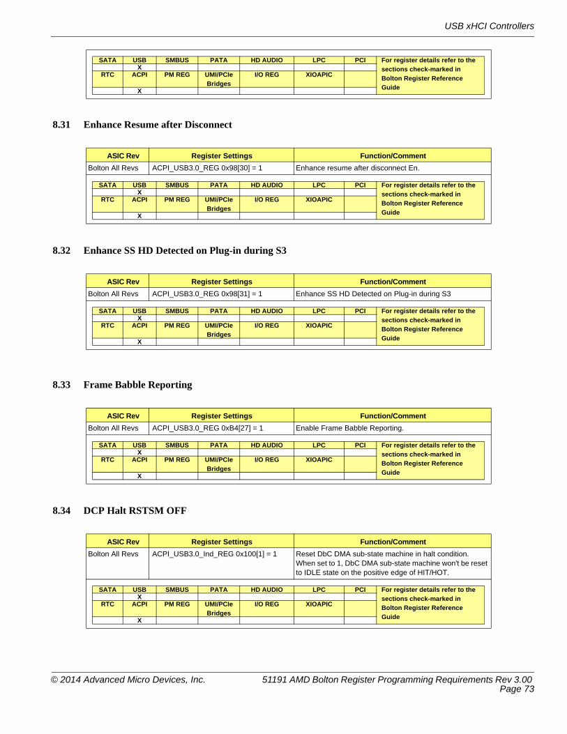
USB xHCI Controllers
8.31 Enhance Resume after Disconnect
8.32 Enhance SS HD Detected on Plug-in during S3
8.33 Frame Babble Reporting
8.34 DCP Halt RSTSM OFF
ASIC Rev Register Settings Function/CommentBolton All Revs ACPI_USB3.0_REG 0x98[30] = 1 Enhance resume after disconnect En.
ASIC Rev Register Settings Function/CommentBolton All Revs ACPI_USB3.0_REG 0x98[31] = 1 Enhance SS HD Detected on Plug-in during S3
ASIC Rev Register Settings Function/CommentBolton All Revs ACPI_USB3.0_REG 0xB4[27] = 1 Enable Frame Babble Reporting.
ASIC Rev Register Settings Function/CommentBolton All Revs ACPI_USB3.0_Ind_REG 0x100[1] = 1 Reset DbC DMA sub-state machine in halt condition.
When set to 1, DbC DMA sub-state machine won't be reset to IDLE state on the positive edge of HIT/HOT.
SATA USB SMBUS PATA HD AUDIO LPC PCI For register details refer to the sections check-marked in Bolton Register Reference Guide
XRTC ACPI PM REG UMI/PCIe
BridgesI/O REG XIOAPIC
X
SATA USB SMBUS PATA HD AUDIO LPC PCI For register details refer to the sections check-marked in Bolton Register Reference Guide
XRTC ACPI PM REG UMI/PCIe
BridgesI/O REG XIOAPIC
X
SATA USB SMBUS PATA HD AUDIO LPC PCI For register details refer to the sections check-marked in Bolton Register Reference Guide
XRTC ACPI PM REG UMI/PCIe
BridgesI/O REG XIOAPIC
X
SATA USB SMBUS PATA HD AUDIO LPC PCI For register details refer to the sections check-marked in Bolton Register Reference Guide
XRTC ACPI PM REG UMI/PCIe
BridgesI/O REG XIOAPIC
X
SATA USB SMBUS PATA HD AUDIO LPC PCI For register details refer to the sections check-marked in Bolton Register Reference Guide
XRTC ACPI PM REG UMI/PCIe
BridgesI/O REG XIOAPIC
X
© 2014 Advanced Micro Devices, Inc. 51191 AMD Bolton Register Programming Requirements Rev 3.00 Page 73

USB xHCI Controllers
8.35 Enable DCP DPH Check
8.36 DCP LTSSM Inactive to Rxdetect
8.37 Enhance DCP EP State
8.38 DCP Remote Wakeup Capable
8.39 Enhance SS HS Detection during S3
ASIC Rev Register Settings Function/CommentBolton All Revs ACPI_USB3.0_Ind_REG_ 0x100[2] = 1 Set to 1 to let HSP check if a DPH comes before data
buffer is ready and then be treated as invalid DPH by data buffer controller.
ASIC Rev Register Settings Function/CommentBolton All Revs ACPI_USB3.0_Ind_REG 0x120[3] = 1 Enhance DCP LTSSM Inactive to Rxdetect.
ASIC Rev Register Settings Function/CommentBolton All Revs ACPI_USB3.0_Ind_REG_ 0x100[21] = 1 Set to 1 to clear EP state to DISABLE when DCR is
cleared.
ASIC Rev Register Settings Function/CommentBolton All Revs ACPI_USB3.0_Ind_REG 0x128[0] = 1 Enable DCP Remote Wakeup Capable.
ASIC Rev Register Settings Function/CommentBolton All Revs ACPI_USB3.0_Ind_REG_ 0x48[1] = 1 Set to 1 to enhance SS HS detection during S3.
SATA USB SMBUS PATA HD AUDIO LPC PCI For register details refer to the sections check-marked in Bolton Register Reference Guide
XRTC ACPI PM REG UMI/PCIe
BridgesI/O REG XIOAPIC
X
SATA USB SMBUS PATA HD AUDIO LPC PCI For register details refer to the sections check-marked in Bolton Register Reference Guide
XRTC ACPI PM REG UMI/PCIe
BridgesI/O REG XIOAPIC
X
SATA USB SMBUS PATA HD AUDIO LPC PCI For register details refer to the sections check-marked in Bolton Register Reference Guide
XRTC ACPI PM REG UMI/PCIe
BridgesI/O REG XIOAPIC
X
SATA USB SMBUS PATA HD AUDIO LPC PCI For register details refer to the sections check-marked in Bolton Register Reference Guide
XRTC ACPI PM REG UMI/PCIe
BridgesI/O REG XIOAPIC
X
51191 AMD Bolton Register Programming Requirements Rev 3.00 © 2014 Advanced Micro Devices, Inc.Page 74

USB xHCI Controllers
8.40 Enhance U1 Timer
8.41 Enhance LPM U2Entry State
8.42 Enhance SSIF PME
8.43 Enable ERDY Send when DBC Detects HIT/HOT
ASIC Rev Register Settings Function/CommentBolton All Revs ACPI_USB3.0_Ind REG_ 0x48[14] = 1 Set to 1 to shorten U1 exit response time.
ASIC Rev Register Settings Function/CommentBolton All Revs ACPI_USB3.0_REG 0x24[17] = 1 Enhance LPM U2Entry state.
ASIC Rev Register Settings Function/CommentBolton All Revs ACPI_USB3.0_REG 0x24[15] = 1
ACPI_USB3.0_REG 0x24[14] = 1Enhance SSIF PME.
ASIC Rev Register Settings Function/CommentBolton All Revs ACPI_USB3.0_IND_REG_ 0x100[3] = 1 Set to 1 to support send ERDY to host machine once DBC
detects HIT/HOT is set while it is in flow control.
SATA USB SMBUS PATA HD AUDIO LPC PCI For register details refer to the sections check-marked in Bolton Register Reference Guide
XRTC ACPI PM REG UMI/PCIe
BridgesI/O REG XIOAPIC
X
SATA USB SMBUS PATA HD AUDIO LPC PCI For register details refer to the sections check-marked in Bolton Register Reference Guide
XRTC ACPI PM REG UMI/PCIe
BridgesI/O REG XIOAPIC
X
SATA USB SMBUS PATA HD AUDIO LPC PCI For register details refer to the sections check-marked in Bolton Register Reference Guide
XRTC ACPI PM REG UMI/PCIe
BridgesI/O REG XIOAPIC
X
SATA USB SMBUS PATA HD AUDIO LPC PCI For register details refer to the sections check-marked in Bolton Register Reference Guide
XRTC ACPI PM REG UMI/PCIe
BridgesI/O REG XIOAPIC
X
SATA USB SMBUS PATA HD AUDIO LPC PCI For register details refer to the sections check-marked in Bolton Register Reference Guide
XRTC ACPI PM REG UMI/PCIe
BridgesI/O REG XIOAPIC
X
© 2014 Advanced Micro Devices, Inc. 51191 AMD Bolton Register Programming Requirements Rev 3.00 Page 75

USB xHCI Controllers
8.44 Block HIT/HOT until Service Interval is Done
8.45 Enhance LPM Host Initial L1 Exit
8.46 xHCI ISO Device CRC False Error Detection
ASIC Rev Register Settings Function/CommentBolton All Revs ACPI_USB3.0_Ind_REG_ 0x100[4] = 1 Set to 1 to block HIT/HOT from being seen by the logic until
the current service interval is done.
ASIC Rev Register Settings Function/CommentBolton All Revs ACPI_USB3.0_REG 0x30[29] = 1 Set to 1 to enable Host initiated L1 Exit blocking for remote
wakeup.
ASIC Rev Register Settings Function/CommentStep 1:PCI IND60_Reg00h[16:13] = port number 0000: port0 0001: port1
PCI IND60_Reg00h[9:7] = 'b111;PCI IND60_Reg00h[2:0] = 'b101;PCI IND60_Reg00h[12] = 1;
Step 2:Read IND60_Reg: 00h [17] to ensure it is set to 0
Step 3:PCI IND60_Reg00h[12] = 0;
Step 4:Read IND60_Reg: 00h [17] to ensure it is set to 0
Step 5:PCI IND60_Reg00h[12] = 1;
Programming steps 1-5 should be done for both controllers: bus-0, dev-16, fun-0 and bus-0, dev-16, fun-1
Program for all of the ports in each controller as set by IND60_Reg: 00h [16:13] = port #
SATA USB SMBUS PATA HD AUDIO LPC PCI For register details refer to the sections check-marked in Bolton Register Reference Guide
XRTC ACPI PM REG UMI/PCIe
BridgesI/O REG XIOAPIC
X
SATA USB SMBUS PATA HD AUDIO LPC PCI For register details refer to the sections check-marked in Bolton Register Reference Guide
XRTC ACPI PM REG UMI/PCIe
BridgesI/O REG XIOAPIC
X
SATA USB SMBUS PATA HD AUDIO LPC PCI For register details refer to the sections check-marked in Bolton Register Reference Guide
XRTC ACPI PM REG UMI/PCIe
BridgesI/O REG XIOAPIC
51191 AMD Bolton Register Programming Requirements Rev 3.00 © 2014 Advanced Micro Devices, Inc.Page 76

USB xHCI Controllers
8.47 Enable FW Enhancement on XHC Clock Control when Memory Power Saving is Disabled
8.48 U2IF Remote Wake Select
8.49 HS Data Toggle Error Handling
8.50 L1 Residency Duration
ASIC Rev Register Settings Function/CommentBolton All Revs ACPI_USB3.0_REG 0x10[13] = 1 Enable FW Enhancement on XHC Clock Control when
Memory Power Saving is disabled.This setting must be programmed for these controllers:bus-0, dev-16, fun-0 / bus-0, dev-16, fun-1
ASIC Rev Register Settings Function/CommentBolton All Revs ACPI_USB3.0_REG 0x24[11] = 1 Select U2IF Remote Wake Mode
0: ROOTHUB can wake from L1 by device remote wake no matter whether RWE is 1 or 01: ROOTHUB cannot wake from L1 by device remote wake if RWE is 0This setting must be programmed for these controllers:bus-0, dev-16, fun-0 / bus-0, dev-16, fun-1
ASIC Rev Register Settings Function/CommentBolton All Revs ACPI_USB3.0_REG 0x24[16] = 1 Enhance HS Data Toggle Error Handling.
This setting must be programmed for these controllers:bus-0, dev-16, fun-0 / bus-0, dev-16, fun-1
ASIC Rev Register Settings Function/CommentBolton All Revs PCI IND60_Reg 0x48[4:0] = 1 When set to 1, the L1 Residency Duration is 100us.
SATA USB SMBUS PATA HD AUDIO LPC PCI For register details refer to the sections check-marked in Bolton Register Reference Guide
XRTC ACPI PM REG UMI/PCIe
BridgesI/O REG XIOAPIC
X
SATA USB SMBUS PATA HD AUDIO LPC PCI For register details refer to the sections check-marked in Bolton Register Reference Guide
XRTC ACPI PM REG UMI/PCIe
BridgesI/O REG XIOAPIC
X
SATA USB SMBUS PATA HD AUDIO LPC PCI For register details refer to the sections check-marked in Bolton Register Reference Guide
XRTC ACPI PM REG UMI/PCIe
BridgesI/O REG XIOAPIC
X
SATA USB SMBUS PATA HD AUDIO LPC PCI For register details refer to the sections check-marked in Bolton Register Reference Guide
XRTC ACPI PM REG UMI/PCIe
BridgesI/O REG XIOAPIC
X
© 2014 Advanced Micro Devices, Inc. 51191 AMD Bolton Register Programming Requirements Rev 3.00 Page 77

USB xHCI Controllers
8.51 CCU Mode
ASIC Rev Register Settings Function/CommentBolton All Revs ACPI_USB3.0_REG 0x10[9] = 0 Set CCU SuperSpeed Remote Wake mode
bus-0, dev-16, fun-0 / bus-0, dev-16, fun-1
SATA USB SMBUS PATA HD AUDIO LPC PCI For register details refer to the sections check-marked in Bolton Register Reference Guide
XRTC ACPI PM REG UMI/PCIe
BridgesI/O REG XIOAPIC
X
51191 AMD Bolton Register Programming Requirements Rev 3.00 © 2014 Advanced Micro Devices, Inc.Page 78

SATA (bus-0, dev-17, fun-0)
9 SATA (bus-0, dev-17, fun-0)Note: Except for Section 9.6, “SATA Identification Programming Sequence for IDE Mode”, all the registers in Section 9 should be restored by SBIOS after S3 resume for the SATA controller if the registers' values are programmed differently from the reset default values.
9.1 SATA Configuration
9.2 Optionally Disable Unused SATA Ports
Note: Different variants support different number of SATA ports. Refer to individual databooks for details.
When software detects that there is no device attached to a port, the port can be disabled to save power.
Note: If a port is configured as eSATA, this section does not apply given that hot plug/unplug support on eSATA requires that the port is not disabled if a device is not attached. For more information on eSATA port settings, please refer to Section 9.7, “External SATA Ports Indication Registers”
ASIC Rev Register Settings Function/CommentBolton All Revs PM_IO 0xDA [0] = 1
(default)Enable the SATA controller.Whenever SATA controller is being enabled by programming this field from ‘0’ to ‘1’, it is strongly recommended that a CF9 soft reset to be issued to reset the controller to a proper operational state.
SATA_PCI_Config 0x40 [0] = 0 This bit needs to be cleared to convert the subclass code register to read-only. Refer to section SATA Subclass Programming Sequence for the SATA subclass programming sequence.
SATA_PCI_Config 0x44 [0] = 1 Enable the SATA watchdog timer register prior to the SATA BIOS POST. Note: The system may hang during post if this register is not set correctly.
SATA_PCI_Config 0x48 [31] = 1 Enable IDE DMA read enhancement
ASIC Rev Register Settings Function/CommentBolton All Revs SATA_PCI_Config 0x40 [16] = 1 When set, SATA port 0 is disabled, and port 0 clock is shut down.
SATA_PCI_Config 0x40 [17] = 1 When set, SATA port 1 is disabled, and port 1 clock is shut down.
SATA_PCI_Config 0x40 [18] = 1 When set, SATA port 2 is disabled, and port 2 clock is shut down.
SATA_PCI_Config 0x40 [19] = 1 When set, SATA port 3 is disabled, and port 3 clock is shut down.
SATA_PCI_Config 0x40 [20] = 1 When set, SATA port 4 is disabled, and port 4 clock is shut down.
SATA_PCI_Config 0x40 [21] = 1 When set, SATA port 5 is disabled, and port 5 clock is shut down.
SATA_PCI_Config 0x40 [22] = 1 When set, SATA port 6 is disabled, and port 6 clock is shut down.
SATA_PCI_Config 0x40 [23] = 1 When set, SATA port 7 is disabled, and port 7 clock is shut down.
Note: Some board designs may choose to disable unused SATA ports to reduce power consumption.
SATA USB SMBUS PATA HD AUDIO LPC PCI For register details refer to the sections check-marked in Bolton Register Reference Guide
XRTC ACPI PM REG UMI/PCIe
BridgesI/O REG XIOAPIC
X
SATA USB SMBUS PATA HD AUDIO LPC PCI For register details refer to the sections check-marked in Bolton Register Reference Guide
XRTC ACPI PM REG UMI/PCIe
BridgesI/O REG XIOAPIC
© 2014 Advanced Micro Devices, Inc. 51191 AMD Bolton Register Programming Requirements Rev 3.00 Page 79
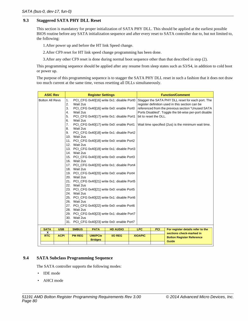
SATA (bus-0, dev-17, fun-0)
9.3 Staggered SATA PHY DLL Reset
This section is mandatory for proper initialization of SATA PHY DLL. This should be applied at the earliest possible BIOS routine before any SATA initialization sequence and after every reset to SATA controller due to, but not limited to, the following:
1.After power up and before the HT link Speed change.
2.After CF9 reset for HT link speed change programming has been done.
3.After any other CF9 reset is done during normal boot sequence other than that described in step (2).
This programming sequence should be applied after any resume from sleep states such as S3/S4, in addition to cold boot or power up.
The purpose of this programming sequence is to stagger the SATA PHY DLL reset in such a fashion that it does not draw too much current at the same time, versus resetting all DLLs simultaneously.
9.4 SATA Subclass Programming Sequence
The SATA controller supports the following modes:
• IDE mode
• AHCI mode
ASIC Rev Register Settings Function/CommentBolton All Revs 1. PCI_CFG 0x40[16] write 0x1: disable Port0
2. Wait 2us3. PCI_CFG 0x40[16] write 0x0: enable Port04. Wait 2us5. PCI_CFG 0x40[17] write 0x1: disable Port16. Wait 2us7. PCI_CFG 0x40[17] write 0x0: enable Port18. Wait 2us9. PCI_CFG 0x40[18] write 0x1: disable Port210. Wait 2us11. PCI_CFG 0x40[18] write 0x0: enable Port212. Wait 2us13. PCI_CFG 0x40[19] write 0x1: disable Port314. Wait 2us15. PCI_CFG 0x40[19] write 0x0: enable Port316. Wait 2us17. PCI_CFG 0x40[20] write 0x1: disable Port418. Wait 2us19. PCI_CFG 0x40[20] write 0x0: enable Port420. Wait 2us21. PCI_CFG 0x40[21] write 0x1: disable Port522. Wait 2us23. PCI_CFG 0x40[21] write 0x0: enable Port524. Wait 2us25. PCI_CFG 0x40[22] write 0x1: disable Port626. Wait 2us27. PCI_CFG 0x40[22] write 0x0: enable Port628. Wait 2us29. PCI_CFG 0x40[23] write 0x1: disable Port730. Wait 2us31. PCI_CFG 0x40[23] write 0x0: enable Port7
Stagger the SATA PHY DLL reset for each port. The register definition used in this section can be referenced from the previous section “Unused SATA Ports Disabled”. Toggle the bit-wise per-port disable bit to reset the DLL.
Wait time specified (2us) is the minimum wait time.
SATA USB SMBUS PATA HD AUDIO LPC PCI For register details refer to the sections check-marked in Bolton Register Reference Guide
XRTC ACPI PM REG UMI/PCIe
BridgesI/O REG XIOAPIC
51191 AMD Bolton Register Programming Requirements Rev 3.00 © 2014 Advanced Micro Devices, Inc.Page 80

SATA (bus-0, dev-17, fun-0)
• RAID mode (some variants do not support RAID, refer to individual databooks)
SBIOS programs the subclass code and the interface register to enable the SATA controller to be represented as the IDE controller, the AHCI controller, or the RAID controller.
9.5 SATA PHY Programming Sequence
The SBIOS should program the SATA controllers in the sequence indicated below. Performing this procedure provides sufficient time for the SATA controllers to correctly complete SATA drive detection. The same procedure is required after the system resumes from the S3 state.
Note: The following recommended PHY values are derived based on AMD Cobia RevC reference board. They will be updated in a timely manner whenever the SI team comes out with a new setting.
ASIC Rev Register Settings Function/CommentBolton All Revs 1. SATA_PCI_ConfigPCI_Config 0x40 [0] =
1Enable the subclass code register (PCI config register 0Ah) and the program interface register (PCI config register 09h) to be programmable.
2. Program SATA Controller mode ina) IDE mode, or SATA_PCI_Config 0x09 = 0x8F (default) SATA_PCI_Config 0x0A = 0x01
b) AHCI mode, or SATA_PCI_Config 0x09 = 0x01 SATA_PCI_Config 0x0A = 0x06
c) RAID mode SATA_PCI_Config 0x09 = 0x00 SATA_PCI_Config 0x0A = 0x04
SBIOS is required to program the subclass code register of the SATA controller to be represented as the IDE, AHCI, or RAID controller.
3. SATA_PCI_Config 0x40 [0] = 0 Clears the bit to convert the subclass code register to be a read-only register. SBIOS is required to complete this step to ensure that the subclass code register be read-only (in order to be PCI compliant).
SATA USB SMBUS PATA HD AUDIO LPC PCI For register details refer to the sections check-marked in Bolton Register Reference Guide
XRTC ACPI PM REG UMI/PCIe
BridgesI/O REG XIOAPIC
© 2014 Advanced Micro Devices, Inc. 51191 AMD Bolton Register Programming Requirements Rev 3.00 Page 81

SATA (bus-0, dev-17, fun-0)
9.6 SATA Identification Programming Sequence for IDE Mode
The following sequence should be included in the SBIOS drive identification loop for SATA drives detection.
ASIC Rev Register Settings Function/CommentBolton All Revs 1. Gen3 Settings:
Port0:a. PCI_Config 0x80 [15:0] = 0x30b. PCI_Config 0x98 [31:0] =0x57A607
Port1:a. PCI_Config 0x80 [15:0] = 0x31b. PCI_Config 0x98 [31:0] =0x57A607
Port2:a. PCI_Config 0x80 [15:0] = 0x32b. PCI_Config 0x98 [31:0] = 0x57A407
Port3:a. PCI_Config 0x80 [15:0]= 0x33b. PCI_Config 0x98 [31:0] = 0x57A407
Port4:a. PCI_Config 0x80 [15:0 ]= 0x34b. PCI_Config 0x98 [31:0] =0x57A607
Port5:a. PCI_Config 0x80 [15:0] = 0x35b. PCI_Config 0x98 [31:0] =0x57A607
Port6:a. PCI_Config 0x80 [15:0] = 0x36b. PCI_Config 0x98 [31:0] = 0x57A403
Port7:a. PCI_Config 0x80 [15:0] = 0x37b. PCI_Config 0x98 [31:0] = 0x57A403
2. Gen2 Settings:SATA_PCI_Config 0x80 [15:0] = 0x0120SATA_PCI_Config 0x98 [31:0] = 0x000713023. Gen1 Settings:SATA_PCI_Config 0x80 [15:0] = 0x0110SATA_PCI_Config 0x98 [31:0] = 0x001741014. Squelch Detector Settings:SATA_PCI_Config 0x80 [15:0] = 0x0110SATA_PCI_Config 0x9C [6:4] =0x25. Restore Gen/Port selection to defaultSATA_PCI_Config 0x80 [15:0] = 0x0010
1. Gen3 settings:Port0 values are based on 2.6" PCB trace length.Port2, 3 values are based on 2.9" PCB trace length.Port4, 5 values are based on 2.4" PCB trace length.Port6, 7 are eSATA ports with 5.9" PCB trace length, so Gen3 is not supported.Programming sequences are provided.
2. Select all 8 ports Gen 2. Fine-tune PHY for Gen 2
3. Select all 8 ports Gen 1. Fine-tune PHY for Gen 1
4. Select all 8 ports, Gen speed is don't-care. Fine-tune squelch detector threshold.
Setting may vary through different board PCB trace lengths.
SATA USB SMBUS PATA HD AUDIO LPC PCI For register details refer to the sections check-marked in Bolton Register Reference Guide
XRTC ACPI PM REG UMI/PCIe
BridgesI/O REG XIOAPIC
51191 AMD Bolton Register Programming Requirements Rev 3.00 © 2014 Advanced Micro Devices, Inc.Page 82

SATA (bus-0, dev-17, fun-0)
ASIC Rev Register Settings Function/CommentBolton All Revs 1. If any of the SATA port status register
SATA_BAR5 + 0x128 [3:0] = 0x3 SATA_BAR5 + 0x1A8 [3:0] = 0x3 SATA_BAR5 + 0x228 [3:0] = 0x3 SATA_BAR5 + 0x2A8 [3:0] = 0x3 SATA_BAR5 + 0x328 [3:0] = 0x3 SATA_BAR5 + 0x3A8 [3:0] = 0x3 SATA_BAR5 + 0x428 [3:0] = 0x3 SATA_BAR5 + 0x4A8 [3:0] = 0x3
Then set SATA_BAR0 + 0x6 = 0xA0 or SATA_BAR0 + 0x6 = 0xB0 or SATA_BAR2 + 0x6 = 0xA0 or SATA_BAR2 + 0x6 = 0xB0 or PATA_BAR0/2 + 0x6 = 0xA0 or PATA_BAR0/2 + 0x6 = 0xB0 or
Go to step (2). Else No drive is attached, exit the detection loop.
SATA_BAR5 + 0x128h : port 0 status registerSATA_BAR5 + 0x1A8h : port 1 status registerSATA_BAR5 + 0x228h : port 2 status registerSATA_BAR5 + 0x2A8h : port 3 status registerSATA_BAR5 + 0x328h : port 4 status registerSATA_BAR5 + 0x3A8h : port 5 status registerSATA_BAR5 + 0x428h : port 6 status registerSATA_BAR5 + 0x4A8h : port 7 status register
SATA host and device serial interface communication is done and ready if the SATA port status register = 0x3.
for SATA controller primary master emulation for SATA controller primary slave emulation for SATA controller secondary master emulation for SATA controller secondary slave emulation for PATA controller primary/secondary master emulation for PATA controller primary/secondary slave emulation
Otherwise, No SATA drive attached or SATA drive is not ready.
2. If SATA_BAR0 + 0x6 = 0xA0 and SATA_BAR0 + 0x7 [7] & [3] = 0 Or SATA_BAR0 + 0x6 = 0xB0 and SATA_BAR0 + 0x7 [7] & [3] = 0 Or SATA_BAR2 + 0x6 = 0xA0 and SATA_BAR2 + 0x7 [7] & [3] = 0 Or SATA_BAR2 + 0x6 = 0xB0 and SATA_BAR2 + 0x7 [7] & [3] = 0 Or PATA_BAR0/2 + 0x6 = 0xA0 and PATA_BAR0/2 + 0x7 [7] & [3] = 0 Or PATA_BAR0/2 + 0x6 = 0xB0 and PATA_BAR0/2 + 0x7 [7] & [3] = 0
then the drive detection is completed Else loop until 30s time out, drive detection fail
SATA_BAR0 + 0x7 [7] & [3] = 0 means primary master device ready
SATA_BAR0 + 0x7 [7] & [3] = 0 means primary slave device ready
SATA_BAR2 + 0x7 [7] & [3] = 0 means secondary master device ready
SATA_BAR2 + 0x7 [7] & [3] = 0 means secondary slave device ready
PATA_BAR0/2 + 0x7 [7] & [3] = 0 means primary /secondary master device ready
PATA_BAR0/2 + 0x7 [7] & [3] = 0 means primary /secondary slave device ready
There is no SATA device attached on the port if time out occurs (see Note).
Note: Most drives do not need 10s timeout. The 10s timeout is only needed for some particularly large capacity SATA drives, which require a longer spin-up time during a cold boot.
SATA USB SMBUS PATA HD AUDIO LPC PCI For register details refer to the sections check-marked in Bolton Register Reference Guide
XRTC ACPI PM REG UMI/PCIe
BridgesI/O REG XIOAPIC
© 2014 Advanced Micro Devices, Inc. 51191 AMD Bolton Register Programming Requirements Rev 3.00 Page 83

SATA (bus-0, dev-17, fun-0)
9.7 External SATA Ports Indication Registers
The following registers need to be programmed for eSATA ports:
ASIC Rev Register Settings Function/CommentBolton All Revs For the ports which are configured as
eSATA:
1. PxCMD.ESP should be set.
To set the register, write:Port 0: SATA BAR5 + 0xF8 [16] = 1Port 1: SATA BAR5 + 0xF8 [17] = 1Port 2: SATA BAR5 + 0xF8 [18] = 1Port 3: SATA BAR5 + 0xF8 [19] = 1Port 4: SATA BAR5 + 0xF8 [20] = 1Port 5: SATA BAR5 + 0xF8 [21] = 1Port 6: SATA BAR5 + 0xF8 [22] = 1Port 7: SATA BAR5 + 0xF8 [23] = 1
2. PxCMD.HPCP should be cleared.
To clear the register, write:Port 0: SATA BAR5 + 0xF8 [0] = 0Port 1: SATA BAR5 + 0xF8 [1] = 0Port 2: SATA BAR5 + 0xF8 [2] = 0Port 3: SATA BAR5 + 0xF8 [3] = 0Port 4: SATA BAR5 + 0xF8 [4] = 0Port 5: SATA BAR5 + 0xF8 [5] = 0Port 6: SATA BAR5 + 0xF8 [6] = 0Port 7: SATA BAR5 + 0xF8 [7] = 0
3. If any of the ports was programmed as an external port, HCAP.SXS should also be set.
To set the register, writeSATA BAR5 + 0xFC[20] = 1
Note: Make sure that the ports declared as eSATA port are not disabled. See Section 8.2.
PxCMD.ESP (External SATA port) and PxCMD.HPCP (Hot Plug Capable port) registers should be programmed to indicate if the port is used for External SATA and if it requires Hot-Plug capability.To program these registers, SATA_PCI_Config x40 [0] needs to be set. After the subclass is programmed, SATA_PCI_Config 0x40 [0] needs to be reset.For example, if port 0 was configured as eSATA, other ports are internal SATA,SATA BAR5 + F8 [23:16] = 00000001(b)SATA BAR5 + F8 [7:0] = 00000000(b)PxCMD.ESP bit is mutually exclusive with PxCMD.HPCP bit in the same port.In general:If no E-SATA ports in system, then HCAP.SXS = 0, else HCAP.SXS = 1. ESP HPCP
eSATA (signal only connector) 1 0 iSATA 0 0
PxCMD ESP located at:SATA BAR5 + port offset + 0x18 [21]PxCMD HPCP located at:SATA BAR5 + port offset + 0x18 [18]
SATA USB SMBUS PATA HD AUDIO LPC PCI For register details refer to the sections check-marked in Bolton Register Reference Guide
XRTC ACPI PM REG UMI/PCIe
BridgesI/O REG XIOAPIC
51191 AMD Bolton Register Programming Requirements Rev 3.00 © 2014 Advanced Micro Devices, Inc.Page 84

SATA (bus-0, dev-17, fun-0)
9.8 Optionally Disable Aggressive Link Power Management
9.9 Optionally Disable Port Multiplier and FIS-based Switching Support
The following register settings provide options to disable support for port multiplier and FIS-based switching.
ASIC Rev Register Settings Function/Comment
Disabling the ALPM will prevent the OS driver from enabling HIPM and DIPM. This setting is required only if both DIPM and HIPM are not required to be supported at the platform level.Bolton All Revs SATA BAR5 + 0xFC [11] = 0 To disable ALPM optionally.
To program these registers, SATA_PCI_Config x40 [0] needs to be set. After that, SATA_PCI_Config 0x40 [0] needs to be reset.Once this bit is cleared, SATA BAR5 + 0x00 [26] will be 0.
When host initiates the power management request, it can be either for slumber or partial mode (the hardware default value indicates it is capable of both partial and slumber modes). There is no special setting for BIOS to achieve the maximum power saving condition; however, there are settings (see below) to disable either partial or slumber mode, if required, to improve performance.
Bolton All Revs 1. Optionally disable PartialRequestSATA BAR5 + 0xFC [1] = 0
2. Optionally disable Slumber RequestSATA BAR5 + 0xFC [26] = 0
1. GHC.PSC will be cleared to 0.
2. GHC.SSC will be cleared to 0.
OS driver will look at these fields to determine if PxCMD.ASP needs to be set. To program these registers, SATA_PCI_config x40 [0] needs to be set. After that, SATA_PCI_config 0x40 [0] needs to be reset.
ASIC Rev Register Settings Function/CommentBolton All Revs SATA BAR5 + 0xFC [12] = 0 Optionally disable port multiplier support
To program this register, SATA_PCI_Config x40 [0] needs to be set. After this register is programmed, SATA_PCI_Config 0x40 [0] needs to be reset.Once this bit is cleared, SATA BAR5 + 0x00 [17] will be 0.
SATA BAR5 + 0xFC [10] = 0SATA BAR5 + 0xF8 [31:24] = 0
Optionally disable FIS-based switching support.To program these registers, SATA_PCI_Config x40 [0] needs to be set. After these registers are programmed, SATA_PCI_Config 0x40 [0] needs to be reset.Once these bits are cleared, SATA BAR5 + 0x00 [16] and SATA BAR5 + port offset + 0x18 [22] will be 0.If AHCI.GHC.SPM (SATA BAR5 + Offset 0x00[17]) =0, then AHCI.GHC.FBSS (SATA BAR5 + Offset 0x00[16]) and AHCI.PxCMD.FBSCP (SATA BAR5 + port Offset 0x18[22]) will be 0 automatically.
SATA USB SMBUS PATA HD AUDIO LPC PCI For register details refer to the sections check-marked in Bolton Register Reference Guide
XRTC ACPI PM REG UMI/PCIe
BridgesI/O REG XIOAPIC
SATA USB SMBUS PATA HD AUDIO LPC PCI For register details refer to the sections check-marked in Bolton Register Reference Guide
RTC ACPI PM_REG UMI/PCIe
BRIDGESI/O REG XIOAPIC
x
© 2014 Advanced Micro Devices, Inc. 51191 AMD Bolton Register Programming Requirements Rev 3.00 Page 85

SATA (bus-0, dev-17, fun-0)
9.10 Disable CCC (Command Completion Coalescing) Support
The following register setting provides an option to disable support for Command Completion Coalescing.
9.11 CCC Interrupt Configuration
Command completion coalescing (CCC) control register is used to configure the CCC feature. Depending on the number of ports that is owned by the AHCI controller, the CCC_CTL.INT field needs to be programmed accordingly so that the corresponding interrupt bit and MSI interrupt vector can be used.
The programming sequence below should be applied regardless of whether CCC is enabled at the time and should be restored after S3 or S4 resume.
9.12 Optionally Disable SATA MSI Capability, Programming of MSI Related Registers, and Disable D3 Power State
9.12.1 SATA MSI Settings
The SATA controller supports message based interrupts. If this feature needs to be disabled, the capability pointer offset needs to be re-programmed from its default setting to prevent the driver from enabling this feature.
Note: MSI capability pointer should be hidden when SATA subclass is configured as IDE (i.e., SATA_PCI_Config 0x0A [7:0] = 0x01).
ASIC Rev Register Settings Function/CommentBolton All Revs SATA_BAR5 + 0xFC [19] = 0 Disable Command Completion Coalescing support.
To program this register, SATA_PCI_Config x40 [0] needs to be set. After this register is programmed, SATA_PCI_Config 0x40 [0] needs to be reset.Once this bit is cleared, SATA BAR5 + 0x00 [7] will be 0.
Register 0xFC[19] controls the CCC capability setting in register BAR5, offset 0 bit 7. Setting it to 0 will make CCC not visible to software. CCC is enabled by default, on power up. BIOS should disable CCC for normal operation.
ASIC Rev Register Settings Function/CommentBolton All Revs 1. SATA_PCI_Config 0x40 [0] = 1
2. SATA_BAR5 + 0xFC [7 :3] = Check the table below :IDE2_Disable 6AHCI 0xFC[7:3] 0 0 0x4 0 1 0x6 1 x 0x83. SATA_PCI_Config 0x40 [0] = 0
1. Unlock programming of CCC_CTL.INT field.2. BAR5 + 0xFC[7:3] will now be able to directly control CCC_CTL.INT (BAR5 + 0x14[7:3]).
3. Lock down the CCC_CTL.INT field.
SATA USB SMBUS PATA HD AUDIO LPC PCI For register details refer to the sections check-marked in Bolton Register Reference Guide
XRTC ACPI PM REG UMI/PCIe
BridgesI/O REG XIOAPIC
SATA USB SMBUS PATA HD AUDIO LPC PCI For register details refer to the sections check-marked in Bolton Register Reference Guide
XRTC ACPI PM REG UMI/PCIe
BridgesI/O REG XIOAPIC
51191 AMD Bolton Register Programming Requirements Rev 3.00 © 2014 Advanced Micro Devices, Inc.Page 86

SATA (bus-0, dev-17, fun-0)
9.12.2 D3 Power State Settings
The SATA controller does not support D3 power state. The capability pointer offset needs to be re-programmed from its default setting to prevent the driver from enabling this feature.
9.12.3 Capability Pointer Settings
The following settings re-program the capability pointer to the recommended start of the capabilities table of supported features.
9.13 Disable SATA FLR Capability
ASIC Rev Register Settings Function/CommentBolton All Revs 1. SATA_PCI_Config 0x40 [0] = 1
2. SATA_PCI_Config 0x34 [7:0] = 0x703. SATA_PCI_Config 0x40 [0] = 0
D3 power state is hidden.MSI capability for SATA is hidden optionally.
1. SATA_PCI_Config 0x40 [0] = 12. SATA_PCI_config 0x34 [7:0] = 0x50
3. Program SATA_PCI_Config 0x50 [19:17] (Multiple Message Capable) according to the table on the comment field. Default of this field is 0x2.
4. SATA_PCI_Config 0x40 [0] = 0
D3 power state is hidden.MSI capability for SATA is visible.
If MSI capability for SATA is visible, program the following registers according to platform configuration.
Multiple Message Capable conveys the information to OS on how many MSI messages are requested. This is 2-based, that is, if MMC=0x2, the number of messages requested is 2 to the power of 2, i.e., 4. Below are the MSI message requirements:IDE mode:msg_required=4 so MMC=0x2
AHCI mode:IDE2_Disable CCC_support msg_required MMC0 0 4 0x20 1 8 0x31 0 8 0x31 1 16 0x4
ASIC Rev Register Settings Function/CommentBolton All Revs 1. SATA_PCI_config 0x40 [0] = 1
2. SATA_PCI_config 0x70 [15:8] = 0x003. SATA_PCI_config 0x40 [0] = 0
Enable write to capability register.Update capability register to hide FLR; FLR is not supported.Disable write to capability register.
SATA USB SMBUS PATA HD AUDIO LPC PCI For register details refer to the sections check-marked in Bolton Register Reference Guide
xRTC ACPI PM REG UMI/PCIe
BridgesI/O REG XIOAPIC
SATA USB SMBUS PATA HD AUDIO LPC PCI For register details refer to the sections check-marked in Bolton Register Reference Guide
XRTC ACPI PM REG UMI/PCIe
BridgesI/O REG XIOAPIC
© 2014 Advanced Micro Devices, Inc. 51191 AMD Bolton Register Programming Requirements Rev 3.00 Page 87

SATA (bus-0, dev-17, fun-0)
9.14 SATA PCI Watchdog Timer
The programming sequence detailed below enables and sets the Watchdog timer.
9.15 SATA/IDE2 Controller Mode and Port Allocation
This section describes the recommended SATA and IDE2 controller mode programming and PCI subclass code combination. Please refer to section 9.3 for subclass code programming in PCI configuration registers.
ASIC Rev Register Settings Function/CommentBolton All Revs SATA_PCI_Config 0x44 [0] = 1
SATA_PCI_Config 0x46 [7:0] = 0x20Enables the Watchdog timer.Sets the Watchdog timer to 0x20.
ASIC Rev Register Settings Function/CommentBolton All Revs SATA Enable =1 (PM_IO 0xDA [0])
SATA 6ACHI =0 (PM_IO 0xDA [1])IDE2 Disable =0 (PM_IO 0xDA [3])
SATA owns Port 0/1/2/3IDE2 owns Port 4/5Subclass Code of SATA / IDE2 could be:SATA IDE2Native IDE Legacy IDELegacy IDE Native IDENative IDE Native IDEAHCI Native or Legacy IDERAID Native or Legacy IDE
SATA Enable =1 (PM_IO 0xDA [0])SATA 6ACHI =0 (PM_IO 0xDA [1])IDE2 Disable =1 (PM_IO 0xDA [3])
SATA owns Port 0/1/2/3/4/5IDE2 DisabledSubclass Code of SATA / IDE2 could be:SATA IDE2Native IDE* DisabledLegacy IDE* DisabledAHCI DisabledRAID Disabled
Note1: Port4/5/ are not accessible if SATA was programmed as IDE controller and IDE2 disabled. Port 4/5 are recommended to be disabled in this configuration.Note2: SATA 6AHCI should not be set if IDE2 controller is disabled since Port4/5 are owned by SATA already.
SATA USB SMBUS PATA HD AUDIO LPC PCI For register details refer to the sections check-marked in Bolton Register Reference Guide
XRTC ACPI PM REG UMI/PCIe
BridgesI/O REG XIOAPIC
SATA USB SMBUS PATA HD AUDIO LPC PCI For register details refer to the sections check-marked in Bolton Register Reference Guide
X XRTC ACPI PM REG UMI/PCIe
BridgesI/O REG XIOAPIC
X
51191 AMD Bolton Register Programming Requirements Rev 3.00 © 2014 Advanced Micro Devices, Inc.Page 88

SATA (bus-0, dev-17, fun-0)
9.16 Optionally Disable SATA PHY PLL Dynamic Shutdown
This section provides an option to disable SATA PHY PLL dynamic shutdown.
IMPORTANT: Bandgap has to be powered on by programming SATA_PCI_config 0x84 [31] to 0. This step is mandatory.
ASIC Rev Register Settings Function/CommentBolton All Revs 1. SATA_PCI_Config 0x84 [30]
2. SATA_PCI_Config 0x84 [31] = 0
1. Turn on/off the advanced power saving feature.
0: No PLL dynamic shutdown. As a result, SATA PHY PLL consumes power even though all the ports are inactive.1: (default) SATA PHY PLL will dynamically shutdown when all the ports are inactive. This “inactivity” includes Slumber Mode and port disable, but excludes Partial Mode.
2. Always power on reference bandgap when PLL power is dynamically shutdown and resumed.
Note: when PHY.PLL.DSHUTDWN is 0, this bit is treated as don’t-care.
This step is mandatory, i.e., bandgap has to be powered on all the time when PLL dynamic shutdown is enabled; otherwise, it will lead to intermittent results.
SATA USB SMBUS PATA HD AUDIO LPC PCI For register details refer to the sections check-marked in Bolton Register Reference Guide
XRTC ACPI PM REG UMI/PCIe
BridgesI/O REG XIOAPIC
© 2014 Advanced Micro Devices, Inc. 51191 AMD Bolton Register Programming Requirements Rev 3.00 Page 89

SATA (bus-0, dev-17, fun-0)
9.17 SATA PHY Reference Clock Selections
This section is dedicated to providing users ways to select SATA PHY reference clock originating from different clock sources.
Currently 3 selections are provided:
• Internal 100MHz differential spread
• Internal 100MHz differential non-spread (default)
• External 100MHz differential non-spread
ASIC Rev Register Settings Function/CommentBolton All Revs Option 1, or
PMIO_Reg 0xDA [5:4] = 0x1PMIO_Reg 0xDA [7:6] = 0x2MISC_Reg 0x40 [25] = 0x1MISC_Reg 0x08 [0] = 0x1MISC_Reg 0x1C [20] = 0x1
Option 2, orPMIO_Reg 0xDA [5:4] = 0x1PMIO_Reg 0xDA [7:6] = 0x2MISC_Reg 0x1C [20] = 0x0
Option 3PMIO_Reg 0xDA [5:4] = 0x2PMIO_Reg 0xDA [7:6] = 0x2
Then reset PHYPCI_Config 0x84 [2] = 0Wait 1msPCI_Config 0x84 [2] = 1
1. This is to select Internal 100MHz differential spread clock from CG1_PLL
a. Select reference clock from internal RDL (default)b. Set SATA PHY divider to div-by-4 (default)c. Unlock CG1 SSC feedback pathsd. Enable CG1 SSC featuree. Select clock from CG1 and output to SATA PHY
2. This is to select the Internal 100MHz differential non-spread clock from CG1_PLL (default setting)
a. Select reference clock from internal RDL (default)b. Set SATA PHY divider to div-by-4 (default)c. Select clock from CG2 and output to SATA PHY (default)
3. This is to select the external differential 100MHz non-spread clock, from external clock chip. This clock path has to be routed on the board, in order for the setting to take effect.
a. Select differential reference clock from an external source, via the PAD_XTALI and PAD_XTALO, to SATA PHYb. Set SATA PHY divider to div-by-4 (default)
4. After Option1, 2, or 3 programming is done, kick off PHY reset sequence to restart PHY
a. Hold low-active reset to 0 to assert reset.b. Wait some timec. Release PHY reset
SATA USB SMBUS PATA HD AUDIO LPC PCI For register details refer to the sections check-marked in Bolton Register Reference Guide
XRTC ACPI PM REG UMI/PCIe
BridgesI/O REG XIOAPIC
X
51191 AMD Bolton Register Programming Requirements Rev 3.00 © 2014 Advanced Micro Devices, Inc.Page 90

SATA (bus-0, dev-17, fun-0)
9.18 Optionally Enable/Disable Unused IDE Channel
This section provides an option to disable unused IDE channel. This setting is only valid when Subclass code of SATA Controller is IDE.
9.19 Enable Hot-removal Detection Enhancement
When the signal amplitude received by the squelch detector inside SATA PHY is too low, the signal valid bit received by the core (given by the squelch detector) will be intermittent, causing hot-removal to be unreliably or falsely detected when there is a device attached. There is a feature designed to enhance the accuracy of hot-removal detection, and this section shows how to enable/disable this feature.
Note: This feature is disabled by default; however, it is strongly recommended that software go through the following programming sequence to enable it.
9.20 Enable E-SATA Power Saving Enhancement
This enhancement is highly recommended for platform that supports External SATA (eSATA)
ASIC Rev Register Settings Function/CommentBolton All Revs SATA_PCI_Config 0x48 [28] = 1
SATA_PCI_Config 0x48 [28] = 0 (default)SATA_PCI_Config 0x48 [29] = 1SATA_PCI_Config 0x48 [29] = 0 (default)
IDE Primary Channel disabled (register level)IDE Primary Channel enabled (register level)IDE Secondary Channel disabled (register level)IDE Secondary Channel enabled (register level)
ASIC Rev Register Settings Function/CommentBolton All Revs 1. PCI_Config 0x80 [8] = 1
2. PCI_Config 0xA8 [0] = 13. PCI_Config 0x80 [8] = 0
1. Enable write-to-all-ports, so that this feature is turned on for all ports.2. Enable this hot-removal detection enhancement feature.3. Disable write-to-all-ports, so that subsequent write to fine tune per-port signals will not be affected.
ASIC Rev Register Settings Function/CommentBolton All Revs SATA_PCI_Config 0x4C [29] = 1 Program this register to enable the E-SATA power saving
feature. When set, the SATA PHY will be placed in low power mode for the ports that are not disabled as in the case of E-SATA ports.
SATA USB SMBUS PATA HD AUDIO LPC PCI For register details refer to the sections check-marked in Bolton Register Reference Guide
XRTC ACPI PM REG UMI/PCIe
BridgesI/O REG XIOAPIC
SATA USB SMBUS PATA HD AUDIO LPC PCI For register details refer to the sections check-marked in Bolton Register Reference Guide
XRTC ACPI PM REG UMI/PCIe
BridgesI/O REG XIOAPIC
SATA USB SMBUS PATA HD AUDIO LPC PCI For register details refer to the sections check-marked in Bolton Register Reference Guide
XRTC ACPI PM REG UMI/PCIe
BridgesI/O REG XIOAPIC
© 2014 Advanced Micro Devices, Inc. 51191 AMD Bolton Register Programming Requirements Rev 3.00 Page 91

SATA (bus-0, dev-17, fun-0)
9.21 Design Enhancement
Programming the following bits is required in order to properly configure the SATA controller.
9.22 Optionally Enable Support for RAS
ASIC Rev Register Settings Function/CommentBolton All Revs SATA PCI_Config 0x4C [18] = 1
SATA PCI_Config 0x4C [20] = 1SATA PCI_Config 0x4C [21] = 1SATA_PCI_Config 0x4C [28:26] = 0x7SATA_PCI_Config 0x4C [31:30] = 0x3SATA_PCI_Config 0x48 [30] = 0x1
HBA enhanced / optimization settings
ASIC Rev Register Settings Function/CommentBolton All Revs Port0:
a. SATA_PCI_Config: 0x48[10:8] = 0x0 b. SATA_PCI_Config: 0x48[18:16] = 0x7Port1: a. SATA_PCI_Config: 0x48[10:8] = 0x1 b. SATA_PCI_Config: 0x48[18:16] = 0x7Port2: a. SATA_PCI_Config: 0x48[10:8] = 0x2 b. SATA_PCI_Config: 0x48[18:16] = 0x7Port3: a. SATA_PCI_Config: 0x48[10:8] = 0x3 b. SATA_PCI_Config: 0x48[18:16] = 0x7Port4: a. SATA_PCI_Config: 0x48[10:8] = 0x4 b. SATA_PCI_Config: 0x48[18:16] = 0x7Port5: a. SATA_PCI_Config: 0x48[10:8] = 0x5 b. SATA_PCI_Config: 0x48[18:16] = 0x7Port6: a. SATA_PCI_Config: 0x48[10:8] = 0x6 b. SATA_PCI_Config: 0x48[18:16] = 0x7Port7: a. SATA_PCI_Config: 0x48[10:8] = 0x7 b. SATA_PCI_Config: 0x48[18:16] = 0x7
Optionally enable the RAS function support.When bits[18:16] are set to 1, RAS is supported. When cleared to 0, RAS is not supported. a. Select port b. Enable RAS function
SATA USB SMBUS PATA HD AUDIO LPC PCI For register details refer to the sections check-marked in Bolton Register Reference Guide
XRTC ACPI PM REG UMI/PCIe
BridgesI/O REG XIOAPIC
SATA USB SMBUS PATA HD AUDIO LPC PCI For register details refer to the sections check-marked in Bolton Register Reference Guide
XRTC ACPI PM REG UMI/PCIe
BridgesI/O REG XIOAPIC
51191 AMD Bolton Register Programming Requirements Rev 3.00 © 2014 Advanced Micro Devices, Inc.Page 92
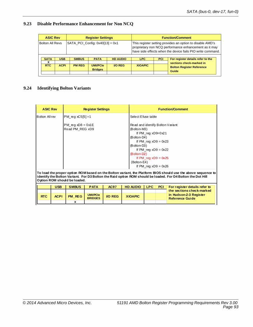
SATA (bus-0, dev-17, fun-0)
9.23 Disable Performance Enhancement for Non NCQ
9.24 Identifying Bolton Variants
ASIC Rev Register Settings Function/CommentBolton All Revs SATA_PCI_Config: 0x40[13] = 0x1 This register setting provides an option to disable AMD’s
proprietary non NCQ performance enhancement as it may have side effects when the device fails PIO write command.
SATA USB SMBUS PATA HD AUDIO LPC PCI For register details refer to the sections check-marked in Bolton Register Reference Guide
XRTC ACPI PM REG UMI/PCIe
BridgesI/O REG XIOAPIC
ASIC Rev Register Settings Function/Comment
Bolton All rev
PM_reg xC5[5] =1 PM_reg xD8 = 0x1E Read PM_REG xD9
Select Efuse table Read and identify Bolton Variant (Bolton-M3) If PM_reg xD9=0x21 (Bolton-D4) If PM_reg xD9 = 0x23 (Bolton-D3) If PM_reg xD9 = 0x22 (Bolton-D2) If PM_reg xD9 = 0x25 (Bolton-E4) If PM_reg xD9 = 0x26
To load the proper option ROM based on the Bolton variant, the Platform BIOS should use the above sequence to identify the Bolton Variant. For D3 Bolton the Raid option ROM should be loaded. For D4 Bolton the Dot Hill Option ROM should be loaded.
USB SMBUS PATA AC97 HD AUDIO LPC PCI For register details refer to the sections check-marked in Hudson-2-3 Register Reference Guide
RTC ACPI PM_REG UMI/PCIe
BRIDGES I/O REG XIOAPIC x
© 2014 Advanced Micro Devices, Inc. 51191 AMD Bolton Register Programming Requirements Rev 3.00 Page 93

SATA IDE Controller 2 (bus-0, dev-20, fun-01)
10 SATA IDE Controller 2 (bus-0, dev-20, fun-01)Except for section 10.1, the registers below should be restored by SBIOS after S3 resume for the SATA IDE Controller2 if the registers' values are programmed differently from the reset default values.
10.1 Optionally Disable SATA IDE Controller 2
10.2 Hide MSI Capability
The programming sequence below disables PATA MSI support.
10.3 Optionally Disable Unused IDE Channel
This section provides an option to disable unused IDE channel.
ASIC Rev Register Settings Function/CommentBolton All Revs PM_IO 0xDA [3] = 1 When this bit is set, the SATA IDE Controller 2 (bus-0, dev-20,
fun-01) will be disabled.Port4/5 are owned by SATA Controller (bus-0, dev-17, fun-00).
ASIC Rev Register Settings Function/CommentBolton All Revs PATA_PCI_Config 0x40 [0] = 1
PATA_PCI_Config 0x34 [7:0] = 0x00PATA_PCI_Config 0x06 [4] = 0x0PATA_PCI_Config 0x40 [0] = 0
Enable modification to Capabilities pointerHide MSI capabilitySet Capabilities List field as logic zeroDisable modification to Capabilities pointer
ASIC Rev Register Settings Function/CommentBolton All Revs PATA_PCI_config 0x48 [28]= 1
PATA_PCI_config 0x48 [28]= 0 (default)
PATA_PCI_config 0x48 [29] = 1PATA_PCI_config 0x48 [29]= 0 (default)
IIDE Primary Channel disabled (register level)IDE Primary Channel enabled (register level)
IDE Secondary Channel disabled (register level)IDE Secondary Channel enabled (register level)
SATA USB SMBUS PATA HD AUDIO LPC PCI For register details refer to the sections check-marked in Bolton Register Reference Guide
RTC ACPI PM REG UMI/PCIe
BridgesI/O REG XIOAPIC
x
SATA USB SMBUS PATA HD AUDIO LPC PCI For register details refer to the sections check-marked in Bolton Register Reference Guide
xRTC ACPI PM REG UMI/PCIe
BridgesI/O REG XIOAPIC
SATA USB SMBUS PATA HD AUDIO LPC PCI For register details refer to the sections check-marked in Bolton Register Reference Guide
XRTC ACPI PM REG UMI/PCIe
BridgesI/O REG XIOAPIC
51191 AMD Bolton Register Programming Requirements Rev 3.00 © 2014 Advanced Micro Devices, Inc.Page 94

HD Audio (bus-0, dev-20, fun-02)
11 HD Audio (bus-0, dev-20, fun-02)
11.1 Enabling/Disabling HD Audio Controller
11.2 HD Audio I/O Configuration
11.3 HD Audio MSI Capability
ASIC Rev Register Settings Function/CommentBolton All Revs PM_Reg 0xEB [0] = 1 0 = Disable the HD Audio controller
1 = Enable the HD Audio controller
ASIC Rev Register Settings Function/CommentBolton All Revs GPIO_Reg 0xA7 [7:0] = 0x3E
GPIO_Reg 0xA8 [7:0] = 0x3EGPIO_Reg 0xA9 [7:0] = 0x3EGPIO_Reg 0xAA [7:0] = 0x3E
See Register Specification for individual bit definition.Bolton HD Audio Controller supports up to codecs with one AZ_SDIN from each codec. The AZ_SDIN pins are shared with GPIO 167 – 170. If a particular pin is to be used for HD Audio functionality, in addition to being configured for Azalia, if the integrated pull-down is to be used rather than external pull-down resistor, the appropriate bits need to be set. For example, if only GPIO167 and GPIO168 are to be used for Azalia, then only 0xA7 and 0xA8 need to be programmed to 0x3E.
ASIC Rev Register Settings Function/CommentBolton All Revs HD Audio PCI_Config 0x45[7:0] = 0x01 Bit [0] = ‘1’ Enables MSI capability
SATA USB SMBUS PATA HD AUDIO LPC PCI For register details refer to the sections check-marked in Bolton Register Reference Guide
RTC ACPI PM REG UMI/PCIe
BridgesI/O REG XIOAPIC
x
SATA USB SMBUS PATA HD AUDIO LPC PCI For register details refer to the sections check-marked in Bolton Register Reference Guide
RTC ACPI PM REG UMI/PCIe
BridgesI/O REG XIOAPIC
x
SATA USB SMBUS PATA HD AUDIO LPC PCI For register details refer to the sections check-marked in Bolton Register Reference Guide
xRTC ACPI PM REG UMI/PCIe
BridgesI/O REG XIOAPIC
© 2014 Advanced Micro Devices, Inc. 51191 AMD Bolton Register Programming Requirements Rev 3.00 Page 95

On-Chip Clock Generator
12 On-Chip Clock Generator
12.1 Internal Clock Generator Enable Status
12.2 PLL 100Mhz Reference Clock Buffer Setting for Internal Clock Generator Mode
12.3 OSC Clock Setting
ASIC Rev Register Settings Function/CommentBolton All Revs MISC_Reg 0x80 [4] = 1
(Read only)Set LPCCLK1 pin strap to ‘1’ to enable internal clock generator. SBIOS should read the PM_MISC_Reg x80[4] as ‘1’ to indicate internal clock generator mode enable.
Note: MISC_Reg is defined at register space AcpiMMioAddr + 0xE00 ~ 0xEFF. The base address “AcpiMMioAddr” is defined at PM_IO x24 [31:12].
ASIC Rev Register Settings Function/CommentBolton All Revs MISC_Reg 0x04 [13] = 1 Set this bit to “1” to turn off 100MHz reference clock input
buffer in internal clock generator mode for power saving.
Note: MISC_Reg is defined at register space AcpiMMioAddr + 0xE00 ~ 0xEFF. The base address “AcpiMMioAddr” is defined at PM_IO x24 [31:12].
ASIC Rev Register Settings Function/CommentBolton All Revs MISC_Reg 0x40 [14] = 1 Set this bit to “1” to select average 14MHz clock provided
by internal PLL in internal clock generator mode and external clock generator mode.
Note: MISC_Reg is defined at register space AcpiMMioAddr + 0xE00 ~ 0xEFF. The base address “AcpiMMioAddr” is defined at PM_IO x24 [31:12].
SATA USB SMBUS PATA HD AUDIO LPC PCI For register details refer to the sections check-marked in Bolton Register Reference Guide
RTC ACPI PM REG UMI/PCIe
BridgesI/O REG XIOAPIC MISC
x X
SATA USB SMBUS PATA HD AUDIO LPC PCI For register details refer to the sections check-marked in Bolton Register Reference Guide
RTC ACPI PM REG UMI/PCIe
BridgesI/O REG XIOAPIC MISC
x X
SATA USB SMBUS PATA HD AUDIO LPC PCI For register details refer to the sections check-marked in Bolton Register Reference Guide
RTC ACPI PM REG UMI/PCIe
BridgesI/O REG XIOAPIC MISC
x X
51191 AMD Bolton Register Programming Requirements Rev 3.00 © 2014 Advanced Micro Devices, Inc.Page 96
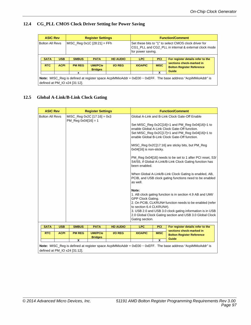
On-Chip Clock Generator
12.4 CG_PLL CMOS Clock Driver Setting for Power Saving
12.5 Global A-Link/B-Link Clock Gating
ASIC Rev Register Settings Function/CommentBolton All Revs MISC_Reg 0x1C [28:21] = FFh Set these bits to "1" to select CMOS clock driver for
CG1_PLL and CG2_PLL in internal & external clock mode for power saving.
Note: MISC_Reg is defined at register space AcpiMMioAddr + 0xE00 ~ 0xEFF. The base address “AcpiMMioAddr” is defined at PM_IO x24 [31:12].
ASIC Rev Register Settings Function/CommentBolton All Revs MISC_Reg 0x2C [17:16] = 0x3
PM_Reg 0x04[16] = 1Global A-Link and B-Link Clock Gate-Off Enable
Set MISC_Reg 0x2C[16]=1 and PM_Reg 0x04[16]=1 to enable Global A-Link Clock Gate-Off function.Set MISC_Reg 0x2C[17]=1 and PM_Reg 0x04[16]=1 to enable Global B-Link Clock Gate-Off function.
MISC_Reg 0x2C[17:16] are sticky bits, but PM_Reg 0x04[16] is non-sticky.
PM_Reg 0x04[16] needs to be set to 1 after PCI reset, S3/S4/S5, if Global A-Link/B-Link Clock Gating function has been enabled.
When Global A-Link/B-Link Clock Gating is enabled, AB, PCIB, and USB clock gating functions need to be enabled as well.
Note:1. AB clock gating function is in section 4.9 AB and UMI/GPP Clock Gating.2. On PCIB, CLKRUN# function needs to be enabled (refer to section 6.4 CLKRUN#).3. USB 2.0 and USB 3.0 clock gating information is in USB 2.0 Global Clock Gating section and USB 3.0 Global Clock Gating section.
Note: MISC_Reg is defined at register space AcpiMMioAddr + 0xE00 ~ 0xEFF. The base address “AcpiMMioAddr” is defined at PM_IO x24 [31:12].
SATA USB SMBUS PATA HD AUDIO LPC PCI For register details refer to the sections check-marked in Bolton Register Reference Guide
RTC ACPI PM REG UMI/PCIe
BridgesI/O REG XIOAPIC MISC
x X
SATA USB SMBUS PATA HD AUDIO LPC PCI For register details refer to the sections check-marked in Bolton Register Reference Guide
RTC ACPI PM REG UMI/PCIe
BridgesI/O REG XIOAPIC MISC
X X
© 2014 Advanced Micro Devices, Inc. 51191 AMD Bolton Register Programming Requirements Rev 3.00 Page 97

On-Chip Clock Generator
12.6 SSC Setting
12.7 A-Link/B-Link Clock Low Speed Mode
12.8 Internal Clock Generator Spread Profile
ASIC Rev Register Settings Function/CommentBolton All Revs MISC_Reg 0x10 [25:24] = 0x1 Select the order of Delta Sigma modulator.
From measurement result, 1st order of Delta Sigma modulator provides better jitter margin.Programming MISC_Reg 0x10 [25:24] = 01b will set Delta Sigma modulator to run at 1st order.
Note: MISC_Reg is defined at register space AcpiMMioAddr + 0xE00 ~ 0xEFF. The base address “AcpiMMioAddr” is defined at PM_IO x24 [31:12].
ASIC Rev Register Settings Function/CommentBolton All Revs MISC_Reg 0x40 [1] = 1 Slow down internal core (A-Link/B-Link) clock for power
saving.0 = Full Speed A-Link/B-Link clock (133Mhz/66Mhz)1 = Slow Speed A-Link/B-Link clock (100Mhz/50lMhz)
Note: MISC_Reg is defined at register space AcpiMMioAddr + 0xE00 ~ 0xEFF. The base address “AcpiMMioAddr” is defined at PM_IO x24 [31:12].
ASIC Rev Register Settings Function/CommentBolton All Revs MISC_Reg 0x08 [0] = 0 Disable Spread Spectrum
a) MISC_Reg 0x40 [25] = 1b) MISC_Reg 0x18 [15:5] = 0x318c) MISC_Reg 0x18 [19:16] = 0d) MISC_Reg 0x10 [23:8] = 0x7296e) MISC_Reg 0x10 [7:0] = 0x94f) MISC_Reg 0x1C [5:0] = 0x00g) MISC_Reg 0x08 [31:28] = 0x9h) MISC_Reg 0x08 [7] = 0i) MISC_Reg 0x08 [8] = 1j) MISC_Reg 0x10 [25:24] = 0x1
The sequence (a) to (j) should be programmed after the Spread Spectrum is disabled. The Spread Spectrum can be enabled after the sequence is programmed.
The Spread Spectrum profile will down spread the PCIe, USB 3.0, Display Port, HDMI / DVI clock outputs, and it applies to internal clock mode only. When using external clock mode, the Spread Spectrum needs to be disabled.
The down spread is 0.373% and is the maximum value supported. (Updated spread from -0.363% to -0.373% for added margin to guard band instrument and process variations.)
MISC_Reg 0x08 [0] = 1 Enable Spread Spectrum
SATA USB SMBUS PATA HD AUDIO LPC PCI For register details refer to the sections check-marked in Bolton Register Reference Guide
RTC ACPI PM REG UMI/PCIe
BridgesI/O REG XIOAPIC MISC
x X
SATA USB SMBUS PATA HD AUDIO LPC PCI For register details refer to the sections check-marked in Bolton Register Reference Guide
RTC ACPI PM REG UMI/PCIe
BridgesI/O REG XIOAPIC MISC
x X
51191 AMD Bolton Register Programming Requirements Rev 3.00 © 2014 Advanced Micro Devices, Inc.Page 98

On-Chip Clock Generator
Note: MISC_Reg is defined at register space AcpiMMioAddr + 0xE00 ~ 0xEFF. The base address "AcpiMMioAddr" is defined at PM_IO 0x24 [31:12].
SATA USB SMBUS PATA HD AUDIO LPC PCI For register details refer to the sections check-marked in Bolton Register Reference Guide
RTC ACPI PM REG UMI/PCIe
BridgesI/O REG XIOAPIC MISC
x X
© 2014 Advanced Micro Devices, Inc. 51191 AMD Bolton Register Programming Requirements Rev 3.00 Page 99

On-Chip Clock Generator
12.9 Enable GPP_CLK_REQ# for Power Saving in Internal Clock Mode
GPP_CLK_P/N pins are powered off when Bolton is strapped to use an external clock, and powered on when strapped to operate in internal clock mode. The GPP_CLK clocks are mapped to corresponding CLK_REQ# pins according to the table below. When in internal clock mode, a selected GPP_CLK can be powered off when the corresponding CLK_REQ# is asserted.
Note: The table above uses GPP_CLK0 as example; other GPP_CLK and the SLT_GFX clocks work similarly with the following register mappings:
GPP_CLK1 clock mapping is at Misc_Reg x00 [7:4]
GPP_CLK2 clock mapping is at Misc_Reg x00 [11:8]
GPP_CLK3 clock mapping is at Misc_Reg x00 [15:12]
GPP_CLK4 clock mapping is at Misc_Reg x00 [19:16]
GPP_CLK5 clock mapping is at Misc_Reg x00 [23:20]
GPP_CLK6 clock mapping is at Misc_Reg x00 [27:24]
GPP_CLK7 clock mapping is at Misc_Reg x00 [31:28]
GPP_CLK8 clock mapping is at Misc_Reg x04 [3:0]
SLT_GFX_CLK clock mapping is at Misc_Reg x04 [7:4]
ASIC Rev Register Settings Function/CommentBolton All Revs
MISC_Reg 0x00[3:0] = 0000 0001 0010 0011 0100 0101 0110 0111 1000 1001 1010 1011 ~ 1110 1111
GPP0_CLKREQ_Mapping:OffCLK_REQ0#CLK_REQ1#CLK_REQ2#CLK_REQ3#CLK_REQ4#CLK_REQ5#CLK_REQ6#CLK_REQ7#CLK_REQ8#CLK_REQGfx#Off, reservedOn (default in internal clock mode)
Note: MISC_Reg is defined at register space AcpiMMioAddr + 0xE00 ~ 0xEFF. The base address “AcpiMMioAddr” is defined at PM_IO x24 [31:12].
SATA USB SMBUS PATA HD AUDIO LPC PCI For register details refer to the sections check-marked in Bolton Register Reference Guide
RTC ACPI PM REG UMI/PCIe
BridgesI/O REG XIOAPIC MISC
X X
51191 AMD Bolton Register Programming Requirements Rev 3.00 © 2014 Advanced Micro Devices, Inc.Page 100

SD Host Controller
13 SD Host Controller
13.1 SD Hold Time Enhancement
13.2 SD Base Clock Frequency
13.3 SD Disable MSI
ASIC Rev Register Settings Function/CommentBolton All Revs SD_DEBUG_Reg 0xB0 [11:10] = 3 Program to '11b' to enable the hold time enhancement for
SD.
ASIC Rev Register Settings Function/CommentBolton All Revs Misc_Reg 0x40 [11:9] = 100b
110b 111b
Specify Misc_Reg 0x40 [11:9] according to trace length:100b when trace length is 6 inches or less; 110b when trace length is between 6 and 11 inches; 111b when trace length is greater than 11 inches.
Note: Less than 6" (board trace + cable) -> 50MHz/25Mhz clock (simulation worst case model has no trace length margin) 6" to 11" (board trace + cable) -> 20% clock frequency reduction (40Mhz/20MHz) (extra 5ns margin) 11" to 24" (board trace + cable) -> 50% clcok frequency reduction (25MHz/12.5MHz)
ASIC Rev Register Settings Function/CommentBolton All Revs SDCFG_reg 0xAC[1] = 0b Program to '0b' to disable the SD MSI capability for SD.
SATA USB SMBUS PATA HD AUDIO LPC PCI For register details refer to the sections check-marked in Bolton Register Reference Guide
RTC ACPI PM REG UMI/PCIe
BridgesI/O REG XIOAPIC SD
X
SATA USB SMBUS PATA HD AUDIO LPC PCI For register details refer to the sections check-marked in Bolton Register Reference Guide
RTC ACPI PM REG UMI/PCIe
BridgesI/O REG XIOAPIC MISC
X
SATA USB SMBUS PATA HD AUDIO LPC PCI For register details refer to the sections check-marked in Bolton Register Reference Guide
RTC ACPI PM REG UMI/PCIe
BridgesI/O REG XIOAPIC SD
X
© 2014 Advanced Micro Devices, Inc. 51191 AMD Bolton Register Programming Requirements Rev 3.00 Page 101