AMD 990FX/990X/970 Register Programming Requirements · © 2012 Advanced Micro Devices, Inc. 48693...
144
AMD 990FX/990X/970 Register Programming Requirements Technical Reference Manual Rev. 3.02 P/N: 48693_990FX-990X-970_rpr_pub_3.02 © 2012 Advanced Micro Devices, Inc.
Transcript of AMD 990FX/990X/970 Register Programming Requirements · © 2012 Advanced Micro Devices, Inc. 48693...

AMD 990FX/990X/970Register Programming Requirements
Technical Reference ManualRev. 3.02
P/N: 48693_990FX-990X-970_rpr_pub_3.02© 2012 Advanced Micro Devices, Inc.

Trademarks
AMD, the AMD Arrow logo, and combinations thereof, are trademarks of Advanced Micro Devices, Inc.
HyperTransport is a licensed trademark of the HyperTransport Technology Consortium.
PCI Express and PCIe are registered trademarks of the PCI-Special Interest Group (PCI-SIG).
Other product names used in this publication are for identification purposes only and may be trademarks of their respective companies.
Disclaimer
The contents of this document are provided in connection with Advanced Micro Devices, Inc. ("AMD") products. AMD makes no representations or warranties with respect to the accuracy or completeness of the contents of this publication and reserves the right to make changes to specifications and product descriptions at any time without notice. No license, whether express, implied, arising by estoppel, or otherwise, to any intellectual property rights are granted by this publication. Except as set forth in AMD's Standard Terms and Conditions of Sale, AMD assumes no liability whatsoever, and disclaims any express or implied warranty, relating to its products including, but not limited to, the implied warranty of merchantability, fitness for a particular purpose, or infringement of any intellectual property right.
AMD's products are not designed, intended, authorized or warranted for use as components in systems intended for surgical implant into the body, or in other applications intended to support or sustain life, or in any other application in which the failure of AMD's product could create a situation where personal injury, death, or severe property or environmental damage may occur. AMD reserves the right to discontinue or make changes to its products at any time without notice.
© 2012 Advanced Micro Devices, Inc. All rights reserved.

Revision History
Date Revision Description
July 2012 3.02 • Replaced ASIC engineering codenames with corresponding marketing names on the cover, and added correlation between the two in Section 1.1.
December 2011 3.01 • Added new step 19.1 to section 4.4.5 “Static PCIe® Port Power Down Control” on page 4- 53
• Updated Table 4-45, “PCIE-GFX Port 0 (Device 2) Power Down Control Programming Sequence,” on page 4-53
• Updated Table 4-47, “PCIE-GFX2 Port 0 (Device 11) Power Down Con-trol Programming Sequence,” on page 4-56
• Updated Table 4-57, “PCIE-GPP2 Power Down Control,” on page 4-62• Updated Table 4-63, “Turning off TXCLK and LCLK,” on page 4-66
September 2011 3.00 Re-issued for public release
July 2010 1.00 First release
© 2012 Advanced Micro Devices, Inc. 48693 AMD 990FX/990X/970 Register Programming Requiremenets Rev 3.02

This page is left blank intentionally.
48693 AMD 990FX/990X/970 Register Programming Requiremenets Rev 3.02 © 2012 Advanced Micro Devices, Inc.

Table of Contents
Chapter 1: Introduction
1.1 About This Manual ..............................................................................................................................................1-1
Chapter 2: I/O Control (IOC)
2.1 RD9xx Device Mapping .......................................................................................................................................2-12.2 Configuration Access to RD9xx Device Registers ..................................................................................................2-12.3 General RD9xx IOC Programming After Bootup....................................................................................................2-12.4 Miscellaneous IOC Features Programming.............................................................................................................2-2
2.4.1 Disabling Bus 0 Device 2, 3, 11, and 12 PCI Bridge ..................................................................................2-22.4.2 Disabling Bus 0 Devices 4-7, 9-10, and 13 PCI Bridges .............................................................................2-22.4.3 Enabling Accesses to Bus 0 Dev 0 Fun 2 Registers (IOMMU Configuration Space).....................................2-32.4.4 Peer-To-Peer (P2P) Modes ......................................................................................................................2-32.4.5 Device ID for Hot-Plug (HP) and PMPME Messages to SB .......................................................................2-32.4.6 Edge-Triggered and Level-Sensitive Interrupt Mode Support .....................................................................2-32.4.7 Forwarding RequesterID (ReqID for Peer-To-Peer (P2P) Requests .............................................................2-32.4.8 JTAG Controller Enable and Security Feature ...........................................................................................2-32.4.9 MCU Enable and Security Feature ...........................................................................................................2-42.4.10 Zero-Byte Read Support ..........................................................................................................................2-4
2.5 Enabling/Disabling Peer-to-Peer Traffic Access .....................................................................................................2-42.6 IOC Dynamic Clock Setup....................................................................................................................................2-42.7 Interrupt Mapping ................................................................................................................................................2-52.8 RD9xx A21 Features ............................................................................................................................................2-6
2.8.1 Forwarding of Host Non-Posted Write Completion Status..........................................................................2-62.8.2 Increase Downstream Message Priority ....................................................................................................2-6
Chapter 3: Clock Settings
3.1 Power Saving Settings ..........................................................................................................................................3-13.1.1 Enabling Dynamic Clocks ......................................................................................................................3-13.1.2 PWM Controller .....................................................................................................................................3-13.1.3 CLKCFG Configuration Space ................................................................................................................3-1
Chapter 4: PCIe Initialization
4.1 Introduction .........................................................................................................................................................4-14.2 Organization ........................................................................................................................................................4-14.3 Architecture and Configuration Topology ..............................................................................................................4-1
4.3.1 Configuration Space Topology.................................................................................................................4-24.3.2 PCIe® Configuration Space ......................................................................................................................4-34.3.3 PCIe® Cores Configuration Topologies.....................................................................................................4-74.3.4 Methods to Bring PCIe® Links to Gen 2 Speed.......................................................................................4-15
4.4 Overall PCIe® Programming Sequence ................................................................................................................4-164.4.1 Power-On Default State.........................................................................................................................4-164.4.2 PCIe® Cores Initialization ......................................................................................................................4-174.4.3 PCIe® Links Training ............................................................................................................................4-404.4.4 PCIe® Power Control.............................................................................................................................4-494.4.5 Static PCIe® Port Power Down Control...................................................................................................4-534.4.6 PCIe® Enumeration and Special Features Programming Sequence ...........................................................4-62
© 2012 Advanced Micro Devices, Inc. 48693 AMD 990FX/990X/970 Register Programming Requirements Rev 3.02TOC-1

4.4.7 Optional Features ................................................................................................................................. 4-664.4.8 PCIe® Workarounds ............................................................................................................................. 4-74
Chapter 5: HTIU Settings
5.1 HT Link Initialization .......................................................................................................................................... 5-15.2 HTIU Indirect Register Space ............................................................................................................................... 5-15.3 CPU Register Access ........................................................................................................................................... 5-1
5.3.1 Normal Registers.................................................................................................................................... 5-15.3.2 PHY Dataport Register Access ................................................................................................................ 5-15.3.3 Link Dependent Registers ....................................................................................................................... 5-1
5.4 Changing to High-Speed Mode ............................................................................................................................. 5-15.4.1 Identifying Supported HT Frequencies ..................................................................................................... 5-15.4.2 Changing to High-Speed HyperTransport™ 1 Mode ................................................................................. 5-25.4.3 Changing to HyperTransport™ 3 Mode ................................................................................................... 5-3
5.5 HT Register Settings ............................................................................................................................................ 5-45.5.1 General Register Settings ........................................................................................................................ 5-45.5.2 UnitID Clumping ................................................................................................................................... 5-65.5.3 Isochronous Flow-Control Mode ............................................................................................................. 5-75.5.4 Family 10h Processor Buffer Allocation Settings ...................................................................................... 5-75.5.5 HyperTransport™ Protocol Checker ........................................................................................................ 5-95.5.6 Transmitter De-emphasis ....................................................................................................................... 5-95.5.7 Low-Power HyperTransport™ Features ................................................................................................... 5-9
Chapter 6: IOAPIC
6.1 IOAPIC Register Spaces ...................................................................................................................................... 6-16.1.1 IOAPIC Registers in the NBCFG Space ................................................................................................... 6-26.1.2 IOAPIC Configuration Registers Space.................................................................................................... 6-26.1.3 IOAPIC Direct Memory Mapped Registers Space..................................................................................... 6-26.1.4 IOAPIC Indirect Memory Mapped Registers Space .................................................................................. 6-3
6.2 IOAPIC Operation ............................................................................................................................................... 6-36.3 Setting Interrupts ................................................................................................................................................. 6-5
6.3.1 Group Interrupt Routing Registers ........................................................................................................... 6-56.3.2 Individual Interrupt Routing .................................................................................................................... 6-86.3.3 Swizzling............................................................................................................................................... 6-96.3.4 Group Assignment................................................................................................................................ 6-106.3.5 IOAPIC Interrupt Interrupt Status Register ............................................................................................. 6-13
6.4 Southbridge Re-Routing Feature ......................................................................................................................... 6-146.4.1 Recommended Usage ........................................................................................................................... 6-15
6.5 Redirection Table Entry Registers ....................................................................................................................... 6-15
Chapter 7: RAS Settings
7.1 Overview ............................................................................................................................................................ 7-1
Chapter 8: IOMMU Initialization
8.1 IOMMU Configuration Space............................................................................................................................... 8-18.1.1 PCI Configuration Space......................................................................................................................... 8-18.1.2 IOMMU Memory Mapped Register Space ............................................................................................... 8-18.1.3 IOMMU L1 Indexed Space ..................................................................................................................... 8-18.1.4 IOMMU L2 Indexed Space ..................................................................................................................... 8-2
8.2 IOMMU Initialization .......................................................................................................................................... 8-28.2.1 IOMMU L1 Initialization ........................................................................................................................ 8-38.2.2 IOMMU L2 Initialization ........................................................................................................................ 8-5
48693 AMD 990FX/990X/970 Register Programming Requirements Rev 3.02 © 2012 Advanced Micro Devices, Inc.TOC-2

8.3 Virtualization ACPI Tables .................................................................................................................................8-128.3.1 I/O Virtualization ACPI Tables Configuration.........................................................................................8-12
8.4 Programming Requirements for OS and Hypervisor Developers ............................................................................8-198.4.1 DTE Setup ...........................................................................................................................................8-198.4.2 Register Programming...........................................................................................................................8-19
© 2012 Advanced Micro Devices, Inc. 48693 AMD 990FX/990X/970 Register Programming Requirements Rev 3.02TOC-3

This page intentionally left blank.
48693 AMD 990FX/990X/970 Register Programming Requirements Rev 3.02 © 2012 Advanced Micro Devices, Inc.TOC-4

Chapter 1Introduction
1.1 About This Manual
This document is intended for BIOS engineers designing BIOSes for systems based on AMD’s 990FX/990X/970 northbridges. Please note that the corresponding ASIC codenames RD990/RD980/RX980 are used throughout this document; in addition, the abbreviation RD9xx is used to designate all three variants when the information applies to all three.
This document describes the register programming requirements needed to ensure the proper functioning of the RD9xx. Use this document in conjunction with AMD 990FX/990X/970 Northbridges BIOS Developer’s Guide and AMD 990FX/990X/970 Northbridges Databook, which gives the details on feature differences amongst the three variants.
If the programming requirements for a particular function/feature differ within different ASIC revisions, the differences will be properly highlighted. Some of the settings indicated in this document are workarounds for problems that are expected to be solved in subsequent ASIC revisions. This document will therefore be updated as frequently as required.
Changes and additions to the previous release of this document are highlighted in red. Refer to Revision History at the beginning of this document for a detailed revision history.
© 2012 Advanced Micro Devices, Inc. 48693 AMD 990FX/990X/970 Register Programming Requirements Rev 3.021-1

About This Manual
This page intentionally left blank.
48693 AMD 990FX/990X/970 Register Programming Requirements Rev 3.02 © 2012 Advanced Micro Devices, Inc.1-2
Chapter 2I/O Control (IOC)
2.1 RD9xx Device Mapping
The RD9xx has the devices indicated below.
• Bus0Dev0Fun0: Host bridge• Bus0Dev0Fun1: Clock control• Bus0Dev0Fun2: IOMMU• Bus0Dev2: PCIE P2P bridge (external graphics)• Bus0Dev3: PCIE P2P bridge• Bus0Dev4: PCIE P2P bridge• Bus0Dev5: PCIE P2P bridge• Bus0Dev6: PCIE P2P bridge• Bus0Dev7: PCIE P2P bridge• Bus0Dev8: NB/SB Link P2P bridge (hidden by default)• Bus0Dev9: PCIE P2P bridge• Bus0Dev10: PCIE P2P bridge• Bus0Dev11: PCIE P2P bridge• Bus0Dev12: PCIE P2P bridge• Bus0Dev13: PCIE P2P bridge
Note: Each device has a P2P bridge header, except Dev0, for which all functions have a PCI device header.
2.2 Configuration Access to RD9xx Device Registers
Refer to the section entitled “Configuration Space” in the AMD family 10h processor BKDG to see how to access Configuration Space as well as Extended Configuration Space.
2.3 General RD9xx IOC Programming After Bootup
• After system boot-up, all registers should keep the default values.• The BIOS starts the bus enumeration, and detects the following: Bus0Dev0Fun0, Bus0Dev0Fun1, Bus0Dev1Fun0,
Bus0Dev1Fun1, Bus0Dev2Fun0, Bus0Dev3Fun0, Bus0Dev4Fun0, Bus0Dev5Fun0, Bus0Dev6Fun0, Bus0Dev7Fun0, Bus0Dev9Fun0, Bus0Dev10Fun0, Bus0Dev11Fun0, Bus0Dev12Fun0. Then, for all of these PCI device headers, or P2P device headers, the BIOS enables IOSpace (0x04[0]) and MemSpaceEn (0x04[1]).
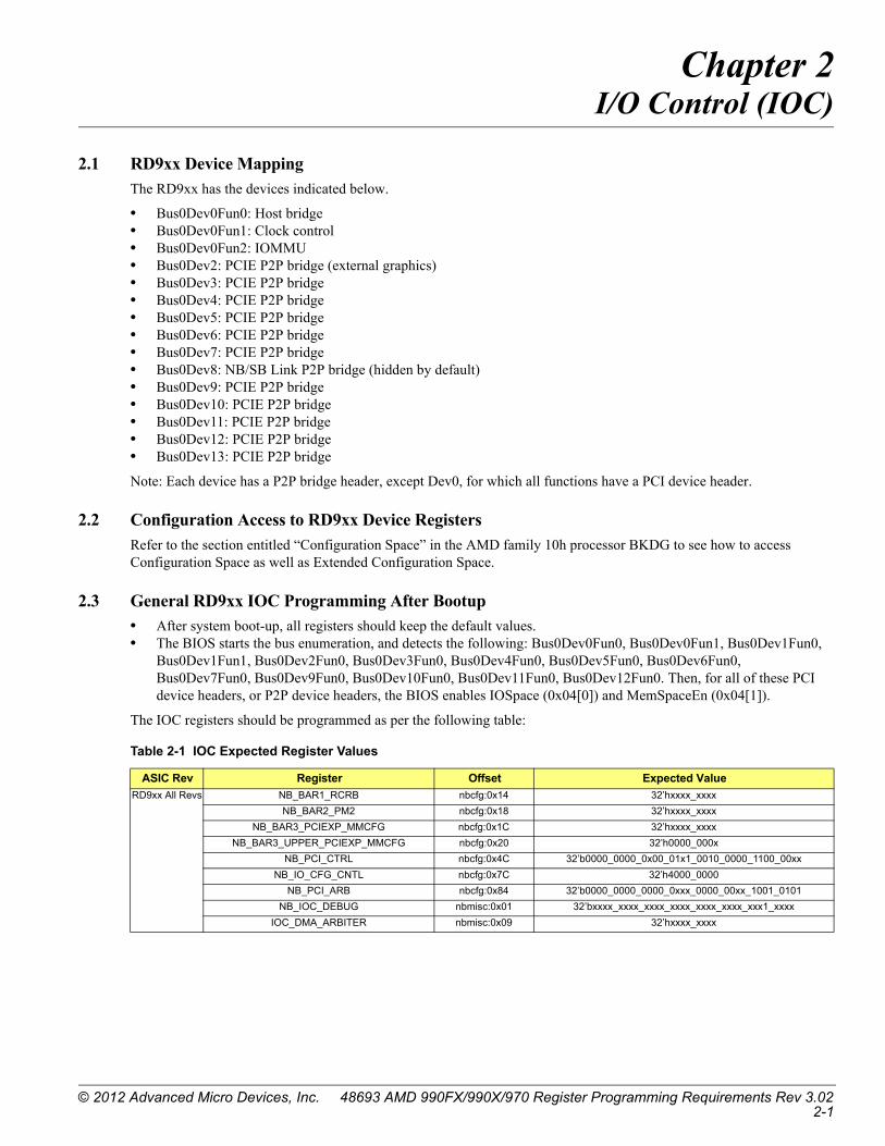
The IOC registers should be programmed as per the following table:
Table 2-1 IOC Expected Register Values
ASIC Rev Register Offset Expected Value
RD9xx All Revs NB_BAR1_RCRB nbcfg:0x14 32’hxxxx_xxxx
NB_BAR2_PM2 nbcfg:0x18 32’hxxxx_xxxx
NB_BAR3_PCIEXP_MMCFG nbcfg:0x1C 32’hxxxx_xxxx
NB_BAR3_UPPER_PCIEXP_MMCFG nbcfg:0x20 32’h0000_000x
NB_PCI_CTRL nbcfg:0x4C 32’b0000_0000_0x00_01x1_0010_0000_1100_00xx
NB_IO_CFG_CNTL nbcfg:0x7C 32’h4000_0000
NB_PCI_ARB nbcfg:0x84 32’b0000_0000_0000_0xxx_0000_00xx_1001_0101
NB_IOC_DEBUG nbmisc:0x01 32’bxxxx_xxxx_xxxx_xxxx_xxxx_xxxx_xxx1_xxxx
IOC_DMA_ARBITER nbmisc:0x09 32’hxxxx_xxxx
© 2012 Advanced Micro Devices, Inc. 48693 AMD 990FX/990X/970 Register Programming Requirements Rev 3.022-1

Miscellaneous IOC Features Programming
2.4 Miscellaneous IOC Features Programming
2.4.1 Disabling Bus 0 Device 2, 3, 11, and 12 PCI Bridge
Note: The GFX ports may be disabled using a register bit or an e-fuse strap.
2.4.2 Disabling Bus 0 Devices 4-7, 9-10, and 13 PCI Bridges
Set any bit according to the information found in Table 2-3.
Table 2-3 Disabling Bus 0 Devices 4-7, 9-10, and 13 PCI Bridges Register Settings
RD9xx All
Revs
IOC_PCIE_CSR_COUNT nbmisc0x0A 32’hxxxx_xxxx
IOC_PCIE_CNTL nbmisc0x0B 32’h0000_0180
IOC_P2P_CNTL nbmisc0x0C 32’bxxxx_0000_0000_0000_0xx1_0111_xxxx_xx00
IOCISOCMAPADDR_LO nbmisc0x0E 32’hxxxx_xxxx
IOCISOCMAPADDR_HI nbmisc0x0F 32’hxxxx_xxxx
NB_BUS_NUM_CNTL nbmisc0x11 32’hxxxx_xxxx
PCIE_CORE_ARB nbmisc0x12 32’h5555_5555
IOC_PERF_COUNT0 nbmisc0x13 32’hxxxx_xxxx
IOC_PERF_COUNT1 nbmisc0x14 32’hxxxx_xxxx
IOC_PERF_CNTL nbmisc0x15 32’h0000_0000
NB_TOM_PCI nbmisc0x16 32’hxxxx_000x
NB_MMIOBASE nbmisc0x17 32’h0000_0000
NB_MMIOLIMIT nbmisc0x18 32’h0000_0000
NB_PROG_DEVICE_REMAP_0 nbmisc0x20 32’h0000_0002
NB_PROG_DEVICE_REMAP_1 nbmisc0x21 32’h0000_0000
IOC_LAT_PERF_CNTR_CNTL nbmisc0x30 32’hxxxx_xx00
IOC_LAT_PERF_CNTR_OUT nbmisc0x31 32’hxxxx_xxxx
NB_BROADCAST_BASE_LO nbmisc0x3A 32’hxxx0_00xx
NB_BROADCAST_BASE_HI nbmisc0x3B 32’h0000_000x
NB_BROADCAST_CNTL nbmisc0x3C 32’hxxxx_xxxx
IOC_JTAG_CNTL nbmisc0x47 32’h0000_xxxx
IOC_PCIE_D2_CNTL nbmisc0x51 32’h0010_0100
IOC_PCIE_D3_CNTL nbmisc0x53 32’h0010_0100
IOC_PCIE_D4_CNTL nbmisc0x55 32’h0010_0100
IOC_PCIE_D5_CNTL nbmisc0x57 32’h0010_0100
IOC_PCIE_D6_CNTL nbmisc0x59 32’h0010_0100
IOC_PCIE_D7_CNTL nbmisc0x5B 32’h0010_0100
IOC_PCIE_D9_CNTL nbmisc0x5D 32’h0010_0100
IOC_PCIE_D10_CNTL nbmisc0x5F 32’h0010_0100
IOC_PCIE_D11_CNTL nbmisc0x61 32’h0010_0100
IOC_PCIE_D12_CNTL nbmisc0x63 32’h0010_0100
Table 2-2 Disabling Bus 0 Device 2, 3, 11, and 12 PCI Bridge Register Settings
ASIC Rev Device Port Bit Settings Disable Strap
RD9xx All Revs Bus 0 Device 2 GFX Port 0 nbmiscind:0x0C[2] EFUSE_DISABLE_GFX_PORT_0
Bus 0 Device 3 GFX Port 1 nbmiscind:0x0C[3] EFUSE_DISABLE_GFX_PORT_1
Bus 0 Device 11 GFX2 Port 0 nbmiscind:0x0C[18] EFUSE_DISABLE_GFX2_PORT_0
Bus 0 Device 12 GFX2 Port 1 nbmiscind:0x0C[19] EFUSE_DISABLE_GFX2_PORT_1
Note: A strap called SLI_DISABLE is also used that could disable Device 3. Either bit, set to 1, would disable the device.
ASIC Rev Device Port Bit Settings
Table 2-1 IOC Expected Register Values (Continued)
ASIC Rev Register Offset Expected Value
48693 AMD 990FX/990X/970 Register Programming Requirements Rev 3.02 © 2012 Advanced Micro Devices, Inc.2-2

Miscellaneous IOC Features Programming
2.4.3 Enabling Accesses to Bus 0 Dev 0 Fun 2 Registers (IOMMU Configuration Space)
Setting nbmiscind:0x75[0] allows access to Busn Dev0 Fun2 PCI configuration space.
When IOMMU is enabled, the bit nbmiscind:0x1[9] should be programmed to 0 for proper behaviour when handling zero-byte reads.
2.4.4 Peer-To-Peer (P2P) Modes
2.4.5 Device ID for Hot-Plug (HP) and PMPME Messages to SB
By setting nbmiscind:0x75[29] to 1 (default is 0), the ReqID[15:0] field in the msg TLP to SB will contain the device number of the P2P bridge that generated the HP or PMPME message, i.e.:
ReqID[15:0] = 8-bit Bus, 5-bit Device, 3-bit Function = {8'b0, Bridge_Device_ID, 3'b0}
2.4.6 Edge-Triggered and Level-Sensitive Interrupt Mode Support
BIOS should program nbmiscind:0x12[19] to 1 to support both interrupt modes.
2.4.7 Forwarding RequesterID (ReqID for Peer-To-Peer (P2P) Requests
This feature should be enabled in SBIOS.
To enable forwarding of the ReqID[15:0] field with a request for P2P transactions, program the following:
• For P2P requests going to external graphics (bus 0, devices 2, 3, 11, and 12), set nbmiscind:0x12[16] = 1 (default 0).
• For P2P requests going to GPP ports (bus 0, devices 4, 5, 6, 7, 9, 10, 13), set nbmiscind:0x12[17] = 1 (default 0).
• To enable Requester ID forwarding in PCIE, set nbmiscind:0x6A[3] to 1 (default 0).
2.4.8 JTAG Controller Enable and Security Feature
Nbmiscind:0x75[11] enables the JTAG interface in IOC. By default, the value of this register bit is 1 (JTAG is enabled). If it is written to 0, posted writes from JTAG will be dropped, while non-posted writes will receive a commit, and reads will be returned with read data set to all 1s.
A SKINIT instruction from the processor will force nbmiscind:0x75[11] to 0. Secure software may write a 1 to re-enable JTAG.
RD9xx All Revs Bus 0 Device 4 GPP Port 0 nbmiscind:0x0C[4]
Bus 0 Device 5 GPP Port 1 nbmiscind:0x0C[5]
Bus 0 Device 6 GPP Port 2 nbmiscind:0x0C[6]
Bus 0 Device 7 GPP Port 3 nbmiscind:0x0C[7]
Bus 0 Device 9 GPP Port 4 nbmiscind:0x0C[16]
Bus 0 Device 10 GPP Port 5 nbmiscind:0x0C[17]
Bus 0 Device 13 GPP2 Port 0 nbmiscind:0x0C[20]
Table 2-4 P2P Modes
ASIC Rev Mode Register Setting Description
RD9xx All Revs
Mode 0 (default) nbmiscind:0x75[10:9] = 2'b00 Legacy mode where a memory write that does not match the memory space of any P2P bridge, the request is dropped in IOC. Memory writes within main memory are unaffected.
Mode 1* nbmiscind:0x75[10:9] = 2'b01 When a memory write does not match the memory space of any P2P bridge, the request is forwarded upstream to HT. Memory writes within main memory are unaffected.
Mode 2* nbmiscind:0x75[10:9] = 2'b10 All memory writes are forwarded to HT.
Reserved nbmiscind:0x75[10:9] = 2'b11 Will mimic P2P mode 0
* Mode 1 or Mode 2 is required for P2P to work in a multi-NB configuration and is also required if it is needed to P2P to PCIE devices behind the SB. BIOS should set the P2P mode to Mode 1, as this will support both single and multi NB configurations.
© 2012 Advanced Micro Devices, Inc. 48693 AMD 990FX/990X/970 Register Programming Requirements Rev 3.022-3
Enabling/Disabling Peer-to-Peer Traffic Access
2.4.9 MCU Enable and Security Feature
Nbmiscind:0x75[12] enables the MCU interface in IOC. By default, the value of the register bit is 1 (MCU is enabled). If bit 12 of the register is written to 0, posted writes from MCU will be dropped, while non-posted writes will receive a commit, and reads will be returned with read data set to all 1s.
A SKINIT instruction from the processor will force nbmiscind:0x75[12] to 0. Secure software may write a 1 to re-enable MCU.
2.4.10 Zero-Byte Read Support
By programming nbmiscind:0x1[8] to 1, IOC will forward the byte-enable (BE) provided by the PCIE DMA access upstream to HTIU, which is 16'b0 for zero-byte reads. This should be enabled by default in system BIOS.
To prevent IOC from zeroing out the address, before sending the request upstream, for zero-byte reads, program nbmiscind:0x1[9] to 1.
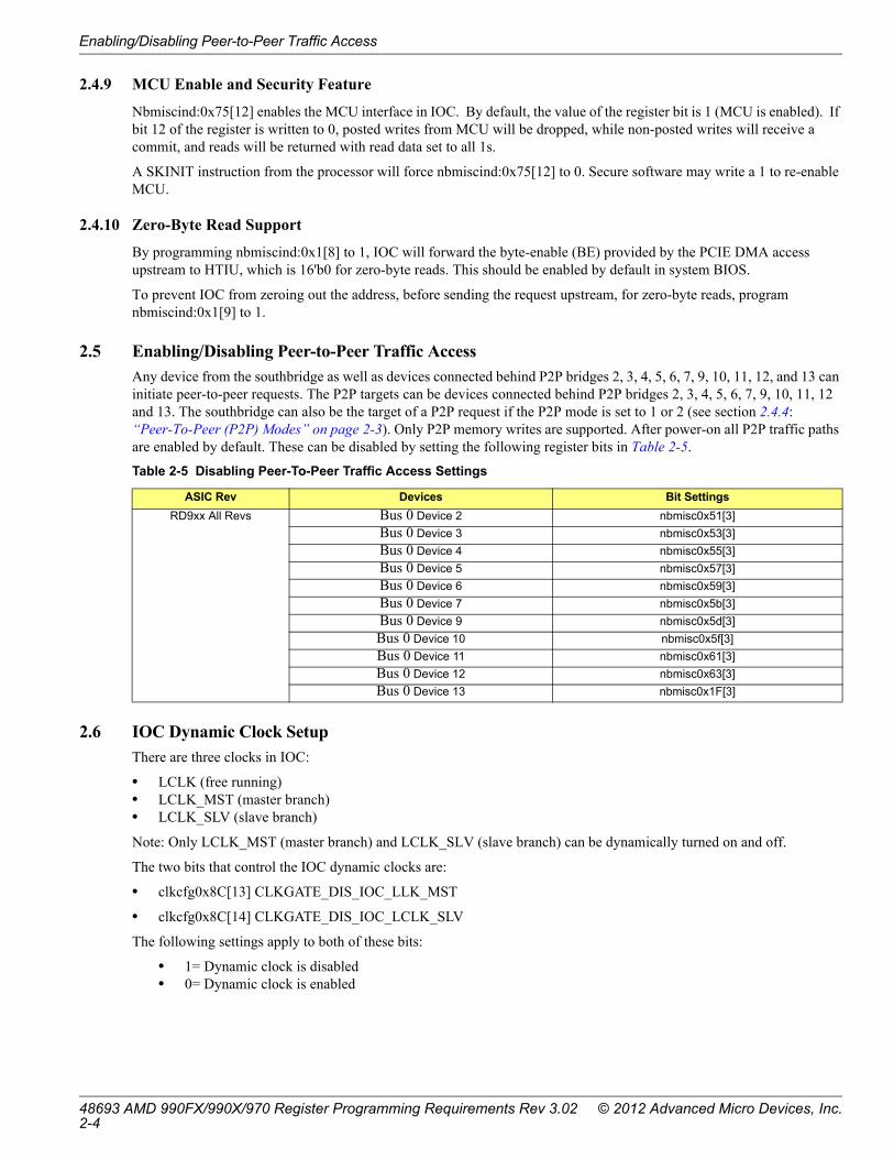
2.5 Enabling/Disabling Peer-to-Peer Traffic Access
Any device from the southbridge as well as devices connected behind P2P bridges 2, 3, 4, 5, 6, 7, 9, 10, 11, 12, and 13 can initiate peer-to-peer requests. The P2P targets can be devices connected behind P2P bridges 2, 3, 4, 5, 6, 7, 9, 10, 11, 12 and 13. The southbridge can also be the target of a P2P request if the P2P mode is set to 1 or 2 (see section 2.4.4: “Peer-To-Peer (P2P) Modes” on page 2-3). Only P2P memory writes are supported. After power-on all P2P traffic paths are enabled by default. These can be disabled by setting the following register bits in Table 2-5.
Table 2-5 Disabling Peer-To-Peer Traffic Access Settings
2.6 IOC Dynamic Clock Setup
There are three clocks in IOC:
• LCLK (free running)• LCLK_MST (master branch)• LCLK_SLV (slave branch)
Note: Only LCLK_MST (master branch) and LCLK_SLV (slave branch) can be dynamically turned on and off.
The two bits that control the IOC dynamic clocks are:
• clkcfg0x8C[13] CLKGATE_DIS_IOC_LLK_MST
• clkcfg0x8C[14] CLKGATE_DIS_IOC_LCLK_SLV
The following settings apply to both of these bits:
• 1= Dynamic clock is disabled• 0= Dynamic clock is enabled
ASIC Rev Devices Bit Settings
RD9xx All Revs Bus 0 Device 2 nbmisc0x51[3]
Bus 0 Device 3 nbmisc0x53[3]
Bus 0 Device 4 nbmisc0x55[3]
Bus 0 Device 5 nbmisc0x57[3]
Bus 0 Device 6 nbmisc0x59[3]
Bus 0 Device 7 nbmisc0x5b[3]
Bus 0 Device 9 nbmisc0x5d[3]
Bus 0 Device 10 nbmisc0x5f[3]
Bus 0 Device 11 nbmisc0x61[3]
Bus 0 Device 12 nbmisc0x63[3]
Bus 0 Device 13 nbmisc0x1F[3]
48693 AMD 990FX/990X/970 Register Programming Requirements Rev 3.02 © 2012 Advanced Micro Devices, Inc.2-4

Interrupt Mapping
2.7 Interrupt Mapping
IOC interrupt mapping only applies when the NB IOAPIC is disabled and interrupts are routed to the SB IOAPIC.
Interrupt mapping is controlled with the bit IntSelMod of the IOC_PCIE_D*_CNTL registers.
Table 2-6 Interrupt Mapping
ASIC Rev Device Behind Internal Bridge # Interrupt Mapping IntSelMod == 1 Interrupt Mapping
RD9xx All Revs 2 INTA -> INTCINTB -> INTDINTC -> INTAINTD -> INTB
INTA -> INTGINTB -> INTHINTC -> INTEINTD -> INTF
3 INTA -> INTDINTB -> INTAINTC -> INTBINTD -> INTC
INTA -> INTHINTB -> INTEINTC -> INTFINTD -> INTG
4 INTA -> INTAINTB -> INTBINTC -> INTCINTD -> INTD
INTA -> INTEINTB -> INTFINTC -> INTGINTD -> INTH
5 INTA -> INTBINTB -> INTCINTC -> INTDINTD -> INTA
INTA -> INTFINTB -> INTGINTC -> INTHINTD -> INTE
6 INTA -> INTCINTB -> INTDINTC -> INTAINTD -> INTB
INTA -> INTGINTB -> INTHINTC -> INTEINTD -> INTF
7 INTA -> INTDINTB -> INTAINTC -> INTBINTD -> INTC
INTA -> INTHINTB -> INTEINTC -> INTFINTD -> INTG
9 INTA -> INTBINTB -> INTCINTC -> INTDINTD -> INTA
INTA -> INTFINTB -> INTGINTC -> INTHINTD -> INTE
10 INTA -> INTCINTB -> INTDINTC -> INTAINTD -> INTB
INTA -> INTGINTB -> INTHINTC -> INTEINTD -> INTF
11 INTA -> INTDINTB -> INTAINTC -> INTBINTD -> INTC
INTA -> INTHINTB -> INTEINTC -> INTFINTD -> INTG
12 INTA -> INTAINTB -> INTBINTC -> INTCINTD -> INTD
INTA -> INTEINTB -> INTFINTC -> INTGINTD -> INTH
13 INTA -> INTBINTB -> INTCINTC -> INTDINTD -> INTA
INTA -> INTFINTB -> INTGINTC -> INTHINTD -> INTE
© 2012 Advanced Micro Devices, Inc. 48693 AMD 990FX/990X/970 Register Programming Requirements Rev 3.022-5

RD9xx A21 Features
2.8 RD9xx A21 Features
2.8.1 Forwarding of Host Non-Posted Write Completion Status
To enable forwarding of the status of host non-posted write completions from PCIe to HTIU, set the following bit to 0x1:
NBMISCIND:0x12[20] = 0x1
2.8.2 Increase Downstream Message Priority
To enable downstream messages to pass downstream host traffic in IOC, set the following bit to 0x1:
NBMISCIND:0x12[21] = 0x1
Table 2-7 RD9xx A21 Features
Feature Programming to Enable Feature
Forwarding of host non-posted write completion status NBMISCIND:0x12[20] = 1
Increase downstream message priority NBMISCIND:0x12[21] = 1
48693 AMD 990FX/990X/970 Register Programming Requirements Rev 3.02 © 2012 Advanced Micro Devices, Inc.2-6

Chapter 3Clock Settings
3.1 Power Saving Settings
3.1.1 Enabling Dynamic Clocks
3.1.2 PWM Controller
There are six PWM controllers mapped to six GPIO pins that can be used for voltage adjustment purpose after boot-up.
Each of the above PWM registers in have the following register fields:
• Bit[0]: Enable the PWM controller• Bits[12:1]: Number of cycles in pulse period of a 100MHz reference clock• Bits[24:13]: Number of high cycles in pulse period of a 100MHz reference clock• Bit[25]: Output enable of the GPIO
3.1.3 CLKCFG Configuration Space
The CLKCFG configuration space (Bus0Dev0Fn1) can be hidden via a register setting. Additionally, the PCI header of CLKCFG (register offsets 0x0 – 0x3F) can be hidden as well. When hidden, write accesses to CLKCFG will have no effect, and read accesses will return 0xFFFFFFFF.
Table 3-1 Dynamic Clocks Settings
ASIC Rev Register Settings
RD9xx All Revs
CFG_CT_CLKGATE_HTIU <clkcfg:0xF8> Controls dynamic clock gating for HTIU/IOC clkcfg:0xF8 [11:0] = 0x0 enable dynamic clockclkcfg:0xF8 [11:0] = 0xfff disable dynamic clock (default)
CLKGATE_DISABLE <clkcfg:0x94> Controls dynamic clock gating for lclk (PCIe)clkcfg:0x94[30:0] = 0x0 enable dynamic clockclkcfg:0x94[30:0] = 0x7FFFFFF7 disable dynamic clock (default)
CLK_TOP_SPARE_C <clkcfg:0xE8> Controls dynamic clock gating for PCIe, cfg and mcu LCLK branchesClkcfg:0xE8[31:25] = 0x7F enable dynamic clockClkcfg:0xE8[31:25] = 0x0 disable dynamic clock (default)
Table 3-2 PWM Controller/GPIO Pins Mapping
ASIC Rev Register Function/Comment
RD9xx All Revs
CLK_TOP_PWM1_CTRL<CLKCFG:0xB0> PWM control on PWM_GPIO1 pin
CLK_TOP_PWM2_CTRL<CLKCFG:0xB4> PWM control on PWM_GPIO2 pin
CLK_TOP_PWM3_CTRL <CLKCFG:0xCC> PWM control on PWM_GPIO3 pin
CLK_TOP_PWM4_CTRL<CLKCFG:0x4C> PWM control on PWM_GPIO4 pin
CLK_TOP_PWM5_CTRL<CLKCFG:0x50> PWM control on PWM_GPIO5 pin
CLK_TOP_PWM6_CTRL<CLKCFG:0x54> PWM control on PWM_GPIO6 pin
Table 3-3 Registers for Hiding/Exposing CLKCFG
ASIC Rev Register Function/Comment
RD9xx All Revs
NB_PCI_CTRL<NBCFG:0x4C> Bit [0] controls hiding of entire CLKCFG spaceNB_PCI_CTRL[0] = 0 Hide CLKCFGNB_PCI_CTRL[0] = 1 Expose CLKCFG
NB_CNTL<NBMISCIND:0x0> Bit [8] controls hiding of CLKCFG PCI header (offsets 0x0 – 0x3F)NB_CNTL[8] = 0 Expose CLKCFG headerNB_CNTL[8] = 1 Hide CLKCFG header
© 2012 Advanced Micro Devices, Inc. 48693 AMD 990FX/990X/970 Register Programming Requirements Rev 3.023-1

Power Saving Settings
SBIOS should fully expose CLKCFG, i.e., set:
NB_PCI_CTRL[0] = 1
NB_CNTL[8] = 0
48693 AMD 990FX/990X/970 Register Programming Requirements Rev 3.02 © 2012 Advanced Micro Devices, Inc.3-2

Chapter 4PCIe Initialization
4.1 Introduction
This chapter describes the programming sequences needed to configure and enable the PCIe® subsystem in RD9xx. The Northbridge PCIe subsystem is highly configurable, designed to support a wide variety of system topologies.
Except for "A-Link Express III", all PCIe links are disabled by default on initial boot up, until system BIOS has the opportunity to reflect the system topology into PCIe subsystem configuration. It is then that all PCIe links are allowed to train and establish point-to-point connections with all the PCIe devices present in the system. Once all PCIe devices are successfully connected in the system, system BIOS is allowed to either complete other tasks or pass control to the Operating System.
4.2 Organization
This chapter essentially comprises two major parts:
• The first part (Section 4.3) describes the general architecture, configuration topology, and configurability of the PCIe subsystem.
• The second part (Section 4.4) details the programming sequences required to train the individual PCIe links and enable various PCIe features.
4.3 Architecture and Configuration Topology
The RD990 PCIe subsystem has 11 configurable PCIe ports that control in total 42 PCIe lanes, in addition to a 4-lane “A-Link Express III” with the Southbridge.
The RD980 PCIe subsystem has 8 configurable PCIe ports that control in total 22 PCIe lanes, in addition to a 4-lane “A-Link Express III” with the Southbridge.
The RX980 PCIe subsystem has 7 configurable PCIe ports that control in total 22 PCIe lanes, in addition to a 4-lane “A-Link Express III” with the Southbridge.
The PCIe ports are divided into two major groups:
• Group 1 is represented by the PCIE-GFX and PCIE-GFX2 cores. This group controls in total 32 PCIe lanes. Each PCIE-GFX and PCIE-GFX2 core controls two PCIe ports (Port 0 and Port 1) with a total of 16 PCIe lanes distributed in either of the following two configurations (note: the nomenclature used here reflects the number of lanes assigned to each of the ports, according to the order “Port 0:Port 1”):
• 8:8
• 16:0
[NOTE 1: PCIE-GFX core in RX980 supports only one PCIe port (Port 0), controlling up to 16 PCIe lanes; therefore, all programming notes in this document related to PCIE-GFX Port 1 are not applicable to that variant.]
[NOTE 2: PCIE-GFX2 is not present in RD980 and RX980, hence all programming notes in this document related to the PCIE-GFX2 core and its associated ports are not applicable to those two variants.]
• Group 2 is represented by the PCIE-GPP, PCIE-GPP2 and PCIE-SB cores. This group controls in total 14 PCIe lanes. The PCIE-SB core controls a single PCIe port (Port 0), dedicated to the Souhtbridge, and is configurable in x1, x2, and x4 PCIe lanes. The PCIE-GPP2 core also controls a single PCIe port (Port 0), configurable in x1, x2, and x4 PCIe lanes. The PCIE-GPP core controls 6 PCIe ports (Port 0 to Port 5), with 6 PCIe lanes distributed across them in the following six possible configurations (the nomenclature used here denotes the number of lanes assigned to each of the ports, according to the order “Port0:Port1:Port2:Port3:Port4:Port5”):
• 4:2:0:0:0:0
• 4:1:1:0:0:0
• 2:2:2:0:0:0
• 2:2:1:1:0:0
© 2012 Advanced Micro Devices, Inc. 48693 AMD 990FX/990X/970 Register Programming Requirements Rev 3.024-1

Architecture and Configuration Topology
• 2:1:1:1:1:0
• 1:1:1:1:1:1
[NOTE: The PCIE-GPP2 core is not present in RD980 and RX980, hence all programming notes in this document related to PCIE-GPP2 are not applicable to those variants.]
4.3.1 Configuration Space Topology
Each RD9xx PCIe port has a virtual PCI-to-PCI bridge structure that connects the host CPU via Northbridge bus 0, as the primary bus number of the bridge, to the PCIe link, which is attached to the bridge secondary bus number. Each of these virtual PCI-to-PCI bridges is referred to as a device. Devices are mapped into the Configuration space such that each will respond to a particular device number.
Figure 4-1illustrates the organization of the PCIe subsystem devices of the RD9xx from the perspective of the system BIOS on the overall PCI/PCIe configuration space. (Refer to notes in section 4.3 above for different ports/lanes support for the three RD9xx variants.)
Figure 4-1 RD9xx PCIe Configuration Space Topology
NB Device 0Function 1
NB Device 0Function 0
P2P Bridge Device
7
P2P Bridge Device
10
P2P Bridge Device
9
P2P Bridge Device
11
P2P Bridge Device
12
P2P Bridge Device
4
P2P Bridge Device
5
P2P Bridge Device
6
P2P Bridge Device
3
P2P Bridge Device
2
1 Lane PCIE
Device
1 Lane PCIE
Device
1 Lane PCIE
Device
1,2,4,8 or 16 Lane PCIE
Device
1,2,4 or 8 Lane PCIE
Device
1,2 or 4 Lane PCIE
Device
1 or 2 Lane PCIE
Device
1 or 2 Lane PCIE
Device
1,2,4 or 8 Lane PCIE
Device
1,2,4,8 or 16 Lane PCIE
Device
P2P Bridge Device
8
1,2 or 4 Lane SB
Secondary Bus#
Secondary Bus#
Secondary Bus#
Secondary Bus#
Secondary Bus#
Secondary Bus#
Secondary Bus#
Secondary Bus#
Secondary Bus#
Secondary Bus#
NB Bus 0
North Bridge RD9xx
PCIE-GPP Core PCIE-GFX2 Core PCIE-SB Core
1,2 or 4 LanePCIE
Device
PCIE-GPP2 Core
Secondary Bus#
PCIE-GFXCore
Secondary Bus#
P2P Bridge Device
13
CPU
Port0Port0Port1Port0Port1Port0Port1Port2Port3Port4Port5Port0
Primary Bus# is
NB Bus 0
Primary Bus# is
NB Bus 0
Primary Bus# is
NB Bus 0
Primary Bus# is
NB Bus 0
Primary Bus# is
NB Bus 0
Primary Bus# is
NB Bus 0
Primary Bus# is
NB Bus 0
Primary Bus# is
NB Bus 0
Primary Bus# is
NB Bus 0
Primary Bus# is
NB Bus 0
Primary Bus# is
NB Bus 0
Primary Bus# is
NB Bus 0
48693 AMD 990FX/990X/970 Register Programming Requirements Rev 3.02 © 2012 Advanced Micro Devices, Inc.4-2

Architecture and Configuration Topology
4.3.2 PCIe® Configuration Space
The RD9xx PCIe configuration space consists of the following four configuration spaces:
• PCI Configuration Space
• PCIE Core Index Space
• PCIE Port Index Space
• PCIE Extended Configuration Space
4.3.2.1 PCI Configuration Space
In order to maintain compatibility with PCI software configuration mechanism, each RD9xx PCIe port has a standard Type 1 virtual PCI-to-PCI bridge header in the PCI configuration space. As shown in Figure 4-1 above, these headers are organized as devices 2 through 13, on PCI bus 0.
[Note: Device 8 (for the Southbridge link) is hidden by default. Before system BIOS turns control over to any system software that may scan the PCI configuration topology, device 8 must be hidden so that it is not detected by system software.]
Figure 4-2 below illustrates the PCI configuration spaces of all RD9xx PCIe ports.
PCI Configuration Space
Bus 0x0, Device 0x2, Function 0x0
PCI Configuration Space
PCI-GFX Port0PCI Config. Space
PCI-GFX Port1PCI Config. Space
PCI-GFX2 Port1PCI Config. Space
PCI-GFX2 Port0PCI Config. Space
0x0
0xFF
PCIE-SB Port0 PCI Config. Space
PCIE-GPP Port0 PCI Config. Space
PCIE-GPP Port2 PCI Config. Space
PCIE-GPP Port3 PCI Config. Space
PCIE-GPP2 Port0 PCI Config. Space
0xE40xE0
PCI Configuration Space
Bus 0x0, Device 0xd, Function 0x0
0x0
0xFF
0xE40xE0
PCI Configuration Space
Bus 0x0, Device 0xm, Function 0x0
0x0
0xFF
PCIE-GPP Port4 PCI Config. Spac
PCIE-GPP Port5 PCI Config. Space
PCIE-GPP Port1 PCI Config. Space
0x34
0x34 PCIE_CAP_PTR
© 2012 Advanced Micro Devices, Inc. 48693 AMD 990FX/990X/970 Register Programming Requirements Rev 3.024-3

Architecture and Configuration Topology
Figure 4-2 PCI Configuration Space
4.3.2.2 PCIe® Core Index Space
RD9xx PCIe Core Index Space is composed of five core index spaces corresponding to the five PCIe cores. Each of them encompasses control and status registers that are generic to all PCIe ports within each PCIe core.
Figure 4-3 PCIe Core Index Space
RD9xx PCIe Core Index Register Space is accessed via an index/data register pair located in the Northbridge Configuration Registers Space. The Index register is located at offset 0xE0 and the Data register is located at 0xE4.
Note: PCIe Core Index Space register descriptions are referenced with the name PCIEIND or BIF_NB.
Hardware has been implemented to provide a mechanism to access each PCIe Core Index Space register independently or jointly, through the programming of bits [18:16] of the index register 0xE0. The encoding is as follows:
• 0xE0[18:16] = 0x4: Read and write access to 0xE4 will be directed at per core index registers for the PCIE-GFX core only.
• 0xE0[18:16] = 0x6: Read and write access to 0xE4 will be directed at per core index register for the PCIE-GFX2 core only.
• 0xE0[18:16] = 0x0: Write access to 0xE4 will be directed at per core index registers for both the PCIE-GFX and the PCIE-GFX2 cores. However, reads will be only issued to the PCIE-GFX core.
• 0xE0[18:16] = 0x7: Read and write access to 0xE4 will be directed at per core index register for the PCIE-GPP core only.
• 0xE0[18:16] = 0x5: Read and write access to 0xE4 will be directed at per core index register for the PCIE-SB core only.
• 0xE0[18:16] = 0x3: Read and write access to 0xE4 will be directed at per core index register for the PCIE-GPP2 core only.
• 0xE0[18:16] = 0x1: Write access to 0xE4 will be directed at per core index registers for the PCIE-GPP, PCIE-GPP2 and the PCIE-SB cores. However, reads will be only issued to the PCIE-SB core.
• 0xE0[18:16] = 0x2: Write access to 0xE4 will be directed at per core index registers for the PCIE-GFX, PCIE-GFX2, PCIE-GPP, PCIE-GPP2 and the PCIE-SB cores. However, reads will be only issued to the PCIE-SB core.
0x0
0xFF
0xE40xE0 NB_PCIE_INDX_ADDR
NB_PCIE_INDX_DATA
NB Configuration Space
Bus 0x0, Device 0x0, Function 0x0
0xE0[18:16]
PCIE-GFX Core Index Space
PCIE-GFX2Core Index Space
PCIE-GPPCore Index Space
PCIE-GPP2Core Index Space
PCIE-SBCore Index Space
0x0
0xFF
PCIE Core Index Space
32
32 32
32
PCIE Core Index Space
Bus 0x0, Device 0x0, Function 0x0
48693 AMD 990FX/990X/970 Register Programming Requirements Rev 3.02 © 2012 Advanced Micro Devices, Inc.4-4

Architecture and Configuration Topology
4.3.2.3 PCIe® Port Index Space
PCIe Port Index Space contains control and status registers that are specific to each port within each PCIe core. Each PCIe device implements its own set of registers in its own instance of this space. Each instance has the same register organization.
To access per port index space registers, each PCIe device has its own Index/Data register pair located in its virtual type 1 PCI-to-PCI bridge configuration space. The Index register is located at offset 0xE0 and the Data register is located at offset 0xE4. Figure 4-4 illustrates PCIe Port Index spaces for all PCIe ports.
[Note: PCIe Port Index Space registers descriptions are referenced with the name PCIEIND_P or BIF_NBP.]
Figure 4-4 PCIe Port Index Space
0xE40xE0
PCI Configuration Space
Bus 0x0, Device 0x2, Function 0x0
PCIE-GFX Port0 Index Space
PCIE-GFX Port1 Index Space
PCIE-GFX2 Port1Index Space
PCIE-GFX2 Port1 Index Space
PCIE-GFX2 Port0Index Space
0x0
0xFF
PCIE Port Index Space32
32
PCIE Port Index Space
Bus 0x0,Device 0x2, Function 0x0
PCIE-SB Port0 Index Space
PCIE-GPP Port0 Index Space
PCIE-GPP Port1 Index Space
PCIE-GPP Port2 Index Space
PCIE-GPP Port3 Index Space
PCIE-GPP Port4 Index Space
PCIE-GPP Port5 Index Space
PCIE-GPP2 Port0 Index Space
PCI Config. SpacePCIE-GFX Port0
PCI Config. SpacePCIE-GFX Port1
PCI Config. SpacePCIE-GFX2 Port1
PCI Config. SpacePCIE-GFX2 Port1
PCI Config. SpacePCIE-GFX2 Port0
0x0
0xFF
PCI Config. SpacePCIE-SB Port0
PCI Config. SpacePCIE-GPP Port0
PCI Config. SpacePCIE-GPP Port1
PCI Config. SpacePCIE-GPP Port2
PCI Config. SpacePCIE-GPP Port3
PCI Config. Space PCIE-GPP Port4
PCI Config. SpacePCIE-GPP Port5
PCI Config. SpacePCIE-GPP2 Port0
0xE40xE0
PCI Configuration Space
Bus 0x0, Device 0xd, Function 0x0
0x0
0xFF
0xE40xE0
PCI Configuration Space
Bus 0x0, Device 0xm, Function 0x0
0x0
0xFF
32
32Bus 0x0,Device 0xd, Function 0x0
PCIE Port Index Space
0xFF
0x0
0xFF
PCIE Port Index Space32
32Bus 0x0,Device 0xm, Function 0x0
© 2012 Advanced Micro Devices, Inc. 48693 AMD 990FX/990X/970 Register Programming Requirements Rev 3.024-5

Architecture and Configuration Topology
4.3.2.4 PCIe® Extended Configuration Space
PCIe extends the PCI configuration space from 256 bytes to 4096 bytes as shown in Figure 4-5 below. Extended PCIe Configuration space memory maps 4KB for each device. The first 256 bytes of each 4KB are the same as PCI 2.3 configuration registers, and the remaining 3840 bytes are PCIe specific configuration registers.
Figure 4-5 PCIe Extended Configuration Space
PCI-GFX Port1PCI Config. Space
PCI-GFX Port1PCIe Ext. Config.
Space
PCI Configuration Space
Bus 0x0, Device 0x2, Function 0x0
PCI Express ExtendedConfiguration Space
PCI-GFX Port0PCI Config. Space
0x0
0xFF
PCI-GFX Port0PCIe Ext. Config.
Space
0xFFF
PCI ExpressExtended
Configuration Space
Bus 0x0, Device 0x2, Function 0x0
PCI Configuration Space
Bus 0x0, Device 0xd, Function 0x0
PCI-GPP2 Port0PCI Config. Space
0x0
0xFF
PCI-GPP2 Port0PCIe Ext. Config.
Space
0xFFF
PCI ExpressExtended
Configuration Space
Bus 0x0, Device 0xd, Function 0x0
48693 AMD 990FX/990X/970 Register Programming Requirements Rev 3.02 © 2012 Advanced Micro Devices, Inc.4-6

Architecture and Configuration Topology
4.3.3 PCIe® Cores Configuration Topologies
4.3.3.1 PCIE-GFX and PCIE-GFX2 Cores Configuration Topologies
Each RD9xx PCIE-GFX and PCIE-GFX2 core supports two PCIe configuration topologies. On initial boot up, the default configuration topology for both cores is single port configuration, in which each core controls a single port with up to 16 lanes. The alternative configuration topology is dual port configuration in which each core controls two ports with up to 8 lanes.
Each PCIE-GFX and PCIE-GFX2 core supports either one standard type-1 virtual PCI-to-PCI bridge header in single port configuration or two standard type-1 PCI-to-PCI bridge headers in dual port configuration. For PCI-GFX core, this is Device 2 in single port configuration or alternatively Device 2 and Device 3 in dual port configuration attached to bus 0 in the configuration space of the PCIE-GFX core. For PCI-GFX2 core, this is Device 11 in single port configuration or alternatively Device 11 and Device 12 in dual port configuration attached to bus 0 in the configuration space of the PCIE-GFX2 core.
Table 4-1 below lists the two PCIE-GFX configuration topologies, the Northbridge configuration space register controlling these configuration topologies, the PCIe lanes controlled by each port in each configuration topology and the corresponding HOLD_TRAINING bit which must be cleared for each port to allow the associated PCIe link to start training.
Table 4-2 below lists the two PCIE-GFX2 configuration topologies, the Northbridge configuration space register controlling these configuration topologies, the PCIe lanes controlled by each port in each configuration topology, and the corresponding HOLD_TRAINING bit which must be cleared for each port to allow the associated PCIe link to start training.
All PCIe links originating from PCIE-GFX and PCIE-GFX2 cores' ports are disabled by default on initial system boot up until system BIOS configures each core to reflect required customer's configuration topology of the system.
4.3.3.1.1 Reflecting Platform Topology into PCIE-GFX and PCIE-GFX2 Cores Configuration Topologies
A wide variety of customer system topologies may differ from the default configuration topologies of PCIE-GFX and PCIE-GFX2 cores after a power-on reset or warm-reset event; therefore, customer requirements must be translated into selection of each configuration topology of PCIE-GFX and PCIE-GFX2 cores.
The methods for determining the required configurations topologies depend on the level of required platform modularity. If the platform configuration topology is static, then system BIOS may choose to hardcode these requirements into the selection of PCIE-GFX and PCIE-GFX2 cores configurations. For example, if either PCIE-GFX or PCIE-GFX2 core is
Table 4-1 PCIE-GFX Ports Configurations
ASIC RevNBCFG:PCIE_LINK_CFG[8]
· NBMISCIND:0x8PCIE-GFX
Port 0PCIE-GFX Port
1
NBCFG:PCIE_LINK_CFG[5:4] · NBMISCIND:0x8
HOLD_TRAIN*_GFX
RD9xxAll Revs
0 (default, single port,
configuration 16:0)
1, 2, 4, 8 or 16
lanes
N/A PCIE_LINK_CFG[4]HOLD_TRAIN1_GFX (Hold PCIE- GFX Port 0 from Link Training)
1 (dual port,
configuration 8:8)
1, 2, 4 or 8 lanes 1, 2, 4 or 8 lanes PCIE_LINK_CFG[5]HOLD_TRAIN1_GFX (Hold PCIE- GFX Port 1 from Link Training)
Table 4-2 PCIE-GFX2 Ports Configurations
ASIC RevNBCFG:PCIE_LINK_CFG[9]
· NBMISCIND:0x8PCIE-GFX2
Port 0PCIE-GFX2 Port
1
NBCFG:PCIE_LINK_CFG[7:6] · NBMISCIND:0x8
HOLD_TRAIN*GFX2
RD9xx All Revs
0 (default, single port,
configuration 16:0)
1, 2, 4, 8 or 16 lanes N/A PCIE_LINK_CFG[6]HOLD_TRAIN1_GFX2 (Hold PCIE- GFX2 Port 0 from Link Training)
1 (dual port,
configuration 8:8)
1, 2, 4 or 8 lanes 1, 2, 4 or 8 lanes PCIE_LINK_CFG[7]HOLD_TRAIN1_GFX2 (Hold PCIE- GFX2 Port 1 from Link Training)
© 2012 Advanced Micro Devices, Inc. 48693 AMD 990FX/990X/970 Register Programming Requirements Rev 3.024-7

Architecture and Configuration Topology
required to support only one PCIe port, and all of its 16 PCIe lanes are required to be routed only to a single PCIe slot on the platform (or a single endpoint device mounted on the platform), then system BIOS will not have to do any additional programming since the required PCIE-GFX or PCIE-GFX2 core configuration conforms with the default configuration. Another example would be the case where the platform imposes hard requirements of routing the lower 8 PCIe lanes of either core only to one PCIe slot (or a single endpoint device mounted on the platform), and the 8 upper PCIe lanes of the same core to another PCIe slot (or another endpoint device mounted on the platform). In this case system BIOS may choose to hardcode programming of the dual core configuration topology.
Customers' system topologies might require platforms with a higher degree of modularity. Such platforms would require support for automatic detection of configuration topologies required on initial boot up and automatic configurations loading. One way to automatically determine the required configuration topology would be to use two software programmable GPIOs for each PCIE-GFX and PCIE-GFX2 core, each connected to PRSNT# pin of each PCIe slot supported. System BIOS could then read the status of these pins on initial boot up via these GPIOs in order to determine which PCIe slots are populated, and hence make a decision on whether to load 8:8 or 16:0 configuration in each of the cores.
Section 4.3.3.1.1.1 and Section 4.3.3.1.1.2 below detail the programming sequence requirement for system BIOS to load either configuration topology into PCIE-GFX and PCIE-GFX2 cores respectively.
4.3.3.1.1.1 Configuring PCIE-GFX Core Topology
The sequence below should be performed to switch configurations of the PCIE-GFXcore.
Table 4-3 Programming Sequence for Loading Dual PCIE-GFX Core Configuration Topology
ASIC Rev Step Register Settings Function/Comment
RD9xx All Revs
1 NBCFG:PCIE_LINK_CFG[15]=0x1 · NBMISCIND:0x8GLOBAL_RESET_GFX
Set bit [15] to 0x1.
Asserts PCIE-GFX global reset
2 NBCFG:PCIE_NBCFG_REGE[28]=0x1 · NBMISCIND:0x26~STRAP_BIF_all_valid for PCIE-GFX
Set bit [28] to 0x1.
De-asserts STRAP_BIF_all_valid for PCIE-GFX core
3 NBCFG:PCIE_LINK_CFG[8]=0x1 · NBMISCIND:0x8 MULTIPORT_CONFIG_GFX
Set bit [8] to 0x1.
Programs PCIE-GFX to be dual port configuration 8:8.
4 Wait for 2 ms
5 NBCFG:PCIE_NBCFG_REGE[28]=0x0 · NBMISCIND:0x26~STRAP_BIF_all_valid for PCIE-GFX
Clear bit [28] to 0x 0.
Asserts STRAP_BIF_all_valid for PCIE-GFX core
6 NBCFG:PCIE_LINK_CFG[15]=0x0 · NBMISCIND:0x8 GLOBAL_RESET_GFX
Clear bit [15] to 0x0.
De-asserts PCIE-GFX global reset.
7 Follow the procedure for PCIE-GFX common initialization and link training sequence.
48693 AMD 990FX/990X/970 Register Programming Requirements Rev 3.02 © 2012 Advanced Micro Devices, Inc.4-8

Architecture and Configuration Topology
4.3.3.1.1.2 Configuring PCIE-GFX2 Core Topology
The sequence below should be performed to switch configurations of the PCIE-GFX2 core.
4.3.3.2 A-Link Express III, PCIE-GPP and PCIE-GPP2 Configuration Topologies
4.3.3.2.1 A-Link Express III Configuration Topology
The PCIE-SB core controls a single PCIe port with up to 4 PCIe lanes for establishing a high performance link with the Southbridge, known as A-Link Express III. A-Link Express III gets automatically trained upon initial boot up, after Northbridge and then Southbridge power rails become stable, and after the CPU clock becomes stable. Taking Northbridge out of reset automatically triggers training of this link as it is released for training by hardware default.
4.3.3.2.2 PCIE-GPP Core Configuration Topologies
The PCIE-GPP core supports six PCIe configuration topologies controlling six PCIe lanes. This PCIe core is disabled by default on initial boot-up until system BIOS configures the core to reflect the required customer’s configuration topology of the system. The following is a description of the six PCIE-GPP Core Configuration Topologies.
Table 4-4 Programming Sequence for loading dual PCIE-GFX2 Core Configuration Topology
ASIC Rev Step Register Settings Function/Comment
RD9xxAll Revs
1 NBCFG:PCIE_LINK_CFG[13]=0x1 · NBMISCIND:0x8 GLOBAL_RESET_GFX2
Set bit [13] to 0x1.
Asserts PCIE-GFX2 global reset
2 NBCFG:PCIE_NBCFG_REGE[29]=0x1 · NBMISCIND:0x26~STRAP_BIF_all_valid for PCIE_GFX2Set bit [29] to 0x1.
De-asserts STRAP_BIF_all_valid for PCIE-GFX2 core.
3 NBCFG:PCIE_LINK_CFG[9]=0x1 · NBMISCIND:0x8 MULTIPORT_CONFIG_GFX2
Set bit [9] to 0x1.
Programs PCIE-GFX2 to dual port configuration 8:8.
4 Wait for 2 ms
5 NBCFG:PCIE_NBCFG_REGE[29]=0x0 · NBMISCIND:0x26~STRAP_BIF_all_valid for PCIE-GFX2
Clear bit [29] to 0x0.
Asserts STRAP_BIF_all_valid for PCIE-GFX2 core.
6 NBCFG:PCIE_LINK_CFG[13]=0x0 · NBMISCIND:0x8 GLOBAL_RESET_GFX2
Clear bit [13] to 0x0.
De-asserts PCIE-GFX2 global reset.
7 Follow the procedure for PCIE-GFX2 common initialization and link training sequence
© 2012 Advanced Micro Devices, Inc. 48693 AMD 990FX/990X/970 Register Programming Requirements Rev 3.024-9

Architecture and Configuration Topology
4.3.3.2.2.1 PCIE-GPP Configuration 1:1:1:1:1:1
The default PCIE-GPP core configuration controls six PCIe ports, each one with 1 PCIe lane. All six ports are held from link training by default. To allow link training on each PCIE-GPP port, the corresponding HOLD_TRAINING bit must be cleared.
4.3.3.2.2.2 PCIE-GPP Configuration 4:2:0:0:0:0
This configuration controls two PCIe ports, one controlling up to 4 PCIe lanes and the other controlling up to 2 PCIe lanes. To allow link training on each port, the corresponding HOLD_TRAINING bit must be cleared as described below.
4.3.3.2.2.3 PCIE-GPP Configuration 4:1:1:0:0:0
This configuration controls 3 PCIe ports, one controlling up to 4 PCIe lanes, and other two each controlling 1 PCIe lane. To allow link training on each port, the corresponding HOLD_TRAINING bit must be cleared as described below.
Table 4-5 Default PCIE-GPP Configuration 1:1:1:1:1:1
ASIC RevGPP Port
(Static Device Number)Associated Lanes
NBCFG:PCIE_LINK_CFG[26:21] NBMISCIND:0x8 HOLD_TRAIN*_GPP
RD9xx All Revs
GPP Port 0(Dev4)
GPP_RX/TX0 PCIE_LINK_CFG[21]HOLD_TRAIN1_GPP (Hold PCIE-GPP Port 0 from Link Training)
GPP Port 1(Dev5)
GPP_RX/TX1 PCIE_LINK_CFG[22]HOLD_TRAIN2_GPP (Hold PCIE-GPP Port 1 from Link Training)
GPP Port 2(Dev6)
GPP_RX/TX2 PCIE_LINK_CFG[23]HOLD_TRAIN3_GPP (Hold PCIE-GPP Port 2 from Link Training)
RD9xx All Revs
GPP Port 3(Dev7)
GPP_RX/TX3 PCIE_LINK_CFG[24]HOLD_TRAIN4_GPP (Hold PCIE-GPP Port 3 from Link Training)
GPP Port 4(Dev9)
GPP_RX/TX4 PCIE_LINK_CFG[25]HOLD_TRAIN5_GPP (Hold PCIE-GPP Port 4 from Link Training)
GPP Port 5(Dev10)
GPP_RX/TX5 PCIE_LINK_CFG[26]HOLD_TRAIN6_GPP (Hold PCIE-GPP Port 5 from Link Training)
Table 4-6 PCIE-GPP Configuration 4:2:0:0:0:0
ASIC RevGPP Port
(Static Device Number) Associated Lanes
NBCFG:PCIE_LINK_CFG[26:21]· NBMISCIND:0x8
HOLD_TRAIN*_GPP
RD9xx All Revs
GPP Port 0(Dev4)
GPP_RX/TX0GPP_RX/TX1GPP_RX/TX2GPP_RX/TX3
PCIE_LINK_CFG[21]HOLD_TRAIN1_GPP (Hold PCIE-GPP Port 0 from Link Training)
GPP Port 1(Dev9)
GPP_RX/TX4GPP_RX/TX5
PCIE_LINK_CFG[22]HOLD_TRAIN2_GPP (Hold PCIE-GPP Port 1 from Link Training)
Table 4-7 PCIE-GPP Configuration 4:1:1:0:0:0
ASIC RevGPP Port
(Static Device Number)Associated Lanes
NBCFG:PCIE_LINK_CFG[26:21]· NBMISCIND:0x8
HOLD_TRAIN*_GPP
RD9xx All Revs
GPP Port 0(Dev4)
GPP_RX/TX0GPP_RX/TX1GPP_RX/TX2GPP_RX/TX3
PCIE_LINK_CFG[21]HOLD_TRAIN1_GPP (Hold PCIE-GPP Port 0 from Link Training)
GPP Port 1(Dev9)
GPP_RX/TX4 PCIE_LINK_CFG[22]HOLD_TRAIN2_GPP (Hold PCIE-GPP Port 1 from Link Training)
GPP Port 2(Dev10)
GPP_RX/TX5 PCIE_LINK_CFG[23]HOLD_TRAIN3_GPP (Hold PCIE-GPP Port 2 from Link Training)
48693 AMD 990FX/990X/970 Register Programming Requirements Rev 3.02 © 2012 Advanced Micro Devices, Inc.4-10

Architecture and Configuration Topology
4.3.3.2.2.4 PCIE-GPPGPP3a Configuration 2:2:2:0:0:0
This configuration controls 3 PCIe ports, each one controlling up to 2 PCIe lanes. To allow link training on each port, the corresponding HOLD_TRAINING bit must be cleared as described below.
4.3.3.2.2.5 PCIE-GPP Configuration 2:2:1:1:0:0
This configuration controls 4 PCIe ports, the first two controlling up to 2 PCIe lanes and the other two controlling 1 PCIe lane. To allow link training on each port, the corresponding HOLD_TRAINING bit must be cleared as described below.
4.3.3.2.2.6 PCIE-GPP Configuration 2:1:1:1:1:0
This configuration controls 5 PCIe ports, the first one controlling up to 2 PCIe lanes and other 4 controlling 1 PCIe lane. To allow link training on each port, the corresponding HOLD_TRAINING bit must be cleared as described below.
4.3.3.2.3 Reflecting Platform Topology into PCIE-GPP Core Configuration Topologies
PCIE-GPP configuration topology can be selected using either one of the two methods:
• “Pin Straps” method (default method)
• “Software Programming Sequence” method
Table 4-8 PCIE-GPP Configuration 2:2:2:0:0:0
ASIC Rev
GPP Port
(Static Device Number)
Associated LanesNBCFG:PCIE_LINK_CFG[26:21]· NBMISCIND:0x8
HOLD_TRAIN*_GPP
RD9xx All Revs
GPP Port 0(Dev4)
GPP_RX/TX0GPP_RX/TX1
PCIE_LINK_CFG[21]HOLD_TRAIN1_GPP (Hold PCIE-GPP Port 0 from Link Training)
GPP Port 1(Dev6)
GPP_RX/TX2GPP_RX/TX3
PCIE_LINK_CFG[22]HOLD_TRAIN2_GPP (Hold PCIE-GPP Port 1 from Link Training)
GPP Port 2(Dev9)
GPP_RX/TX4GPP_RX/TX5
PCIE_LINK_CFG[23]HOLD_TRAIN3_GPP (Hold PCIE-GPP Port 2 from Link Training)
Table 4-9 PCIE-GPP Configuration 2:2:1:1:0:0
ASIC RevPCIE-GPP Port
(Static Device Number)Associated Lanes
NBCFG:PCIE_LINK_CFG[26:21]· NBMISCIND:0x8
HOLD_TRAIN*_GPP
RD9xx All Revs
GPP Port 0(Dev4)
GPP_RX/TX0GPP_RX/TX1
PCIE_LINK_CFG[21]HOLD_TRAIN1_GPP (Hold PCIE-GPP Port 0 from Link Training)
GPP Port 1(Dev6)
GPP_RX/TX2GPP_RX/TX3
PCIE_LINK_CFG[22]HOLD_TRAIN2_GPP (Hold PCIE-GPP Port 1 from Link Training)
GPP Port 2(Dev9)
GPP_RX/TX4 PCIE_LINK_CFG[23]HOLD_TRAIN3_GPP (Hold PCIE-GPP Port 2 from Link Training)
GPP Port 3(Dev10)
GPP_RX/TX5 PCIE_LINK_CFG[24]HOLD_TRAIN4_GPP (Hold PCIE-GPP Port 3 from Link Training)
Table 4-10 PCIE-GPP Configuration 2:1:1:1:1:0
ASIC RevGPP Port
(Static Device Number)Associated Lanes
NBCFG:PCIE_LINK_CFG[26:21]· NBMISCIND:0x8
HOLD_TRAIN*_GPP
RD9xx All Revs
GPP Port 0(Dev4)
GPP_RX/TX0GPP_RX/TX1
PCIE_LINK_CFG[21]HOLD_TRAIN1_GPP (Hold PCIE-GPP Port 0 from Link Training)
GPP Port 1(Dev6)
GPP_RX/TX2 PCIE_LINK_CFG[22]HOLD_TRAIN2_GPP (Hold PCIE-GPP Port 1 from Link Training)
GPP Port 2(Dev7)
GPP_RX/TX3 PCIE_LINK_CFG[23]HOLD_TRAIN3_GPP (Hold PCIE-GPP Port 2 from Link Training)
GPP Port 3(Dev9)
GPP_RX/TX4 PCIE_LINK_CFG[24]HOLD_TRAIN4_GPP (Hold PCIE-GPP Port 3 from Link Training)
GPP Port 4(Dev10)
GPP_RX/TX5 PCIE_LINK_CFG[25]HOLD_TRAIN1_GPP (Hold PCIE-GPP Port 4 from Link Training)
© 2012 Advanced Micro Devices, Inc. 48693 AMD 990FX/990X/970 Register Programming Requirements Rev 3.024-11

Architecture and Configuration Topology
The selection of the method to load the required PCIE-GPP configuration topology again depends on the level of the required platform modularity. If the required platform configuration is static, then the “Pin Straps” method represents the simpler platform solution to load the required customer topology into PCIE-GPP core with no dependency on any additional software programming. Customers’ system topologies requiring platforms with a higher degree of modularity may find the “Software Programming Sequence” method to be more suitable.
4.3.3.2.3.1 Configuring PCIE-GPP Core Topology Using “Pin Straps” Method
RD9xx offers three dedicated pin straps - DFT_GPIO[4:2] - in order to select one out of six possible PCIE-GPP configurations and reflect the required customer’s system topology into PCIE-GPP core. The pin straps are active low straps and are pulled up internally to operate in default states. In order to change the default value of the pin strap, the strap pins must be pulled down to VSS through a resistor, typically of the value of 3 KOhms.
Table 4-11 shows the pin strap value mapping into PCIE-GPP core configuration and the read-back register of the configuration selected.
Pin straps can be overwritten by a register, regardless of the PCIE-GPP configuration set by pin straps. To switch the PCIE-GPP ports configuration from the one selected by pin straps, use the “Software Programming Sequence” method described below.
Table 4-11 Pin Strap Value and Link Configuration Mapping
Encoding Scheme of PCIE-GPP Configurations using Pin Straps
DFT_GPIO[4:2]
Read-back value of Pin Straps Used to Define PCIE-GPP Configuration
NBCFG:StrapsOutputMux7[4:0] · NBMISCIND:0x67
PCIE-GPP Configuration
0 1 0 01011 1:1:1:1:1:1 (default)
0 0 0 00001 4:2:0:0:0:0
0 0 1 00010 4:1:1:0:0:0
1 0 1 01100 2:2:2:0:0:0
1 0 0 01010 2:2:1:1:0:0
0 1 1 00100 2:1:1:1:1:0
1 1 1 Read back register programmed configuration. PCIE-GPP configuration selected by register programmed value:NBCFG:StrapsOutputMux7[4:0] · NBMISCIND:0x67STRAP_BIF_LINK_CONFIGNOTE: Encoded register value should reflect one of the supported configurations above.
1 1 0 Same as above Same as above
48693 AMD 990FX/990X/970 Register Programming Requirements Rev 3.02 © 2012 Advanced Micro Devices, Inc.4-12

Architecture and Configuration Topology
4.3.3.2.3.2 Configuring PCIE-GPP Core Topology Using “Software Programming Sequence” Method
PCIE-GPP core configuration topology can be selected by following the programming sequence outlined below.
4.3.3.2.3.3 Programming PCIE-GPP Line Director
PCIE-GPP core has in place a Line Director whose main function is to distribute PCIe lanes to each of PCIe ports in each of the configuration topologies. System BIOS must program PCIE-GPP Line Director depending on the selected PCIE-GPP configuration regardless of the method chosen to load the configuration topology into PCIE-GPP core.
Table 4-13 lists the values that need to be programmed into the Line Director depending on the configuration topology selected. Programming steps required are detailed in Section 4.4 ”Overall PCIe® Programming Sequence” on page 4-16.
Table 4-12 Switching PCIE-GPP Configurations
ASIC Rev Step Register Settings Function/Comment
RD9xxAll Revs
1 NBCFG:PCIE_LINK_CFG[31]=0x1 · NBMISCIND:0x8 GLOBAL_RESET_GPP
Set bit [31] to 0x 1.
Asserts PCIE-GPP global reset.
2 NBCFG:PCIE_NBCFG_REGE[30]=0x1 · NBMISCIND:0x26~STRAP_BIF_all_valid for PCIE-GPP
Set bit [30] to 0x1.
De-asserts STRAP_BIF_all_valid for PCIE-GPP core.
3 Reprogram bits [4:0] to select new PCIE-GPP configuration to override the one defined via pin straps.NBCFG:StrapsOutputMux7 [4:0] · NBMISCIND:0x67
Programs the desired PCIE-GPP configuration. [Refer to Table 4-11 for encoding scheme.]
[Note: This step is performed only if PCIE-GPP ports are to be configured in a configuration different from the one defined via pin straps.]
4 NBCFG:PCIE_NBCFG_REGE[27:0] · NBMISCIND:0x26 Programs PCIE-GPP Line Director.Refer to Table 4-13 for the encoding scheme.
5 NBCFG:PCIE_NBCFG_REGE[30]=0x0 · NBMISCIND:0x26~STRAP_BIF_all_valid for PCIE-GPP
Clear bit [30] to 0x0.
Assert STRAP_BIF_all_valid for PCIE-GPP core.
6 NBCFG:PCIE_LINK_CFG[31]=0x0 · NBMISCIND:0x8 GLOBAL_RESET_GPP
Clear bit [31] to 0x0.
De-asserts PCIE-GPP global reset.
Table 4-13 PCIE-GPP Line Director Mapping
PCIE-GPP Configuration
NBCFG:PCIE_NBCFG_REGE[27:0] · NBMISCIND:0x26
Straight Configuration
Port 0 Lanes
Reversed
Port 1 Lanes
Reversed
Port 2 Lanes
Reversed
Port 0 and Port 1 Lanes
Reversed
Port 0 and Port 2 Lanes
Reversed
Port 1 and Port 2 Lanes
Reversed
Port 0, Port 1 and Port 2
Lanes Reversed
1:1:1:1:1:1 0x2AA3554 N/A N/A N/A N/A N/A N/A N/A
4:2:0:0:0:0 0x055B000 0x055B000 0xF05BA00 N/A 0xF05BA00 N/A N/A N/A
4:1:1:0:0:0 0x215B400 0x215B400 N/A N/A N/A N/A N/A N/A
2:2:2:0:0:0 0xFF0BAA0 0xFFF0AAA 0xFF0BAA0 0xFF0BAA0 0xFFF0AAA 0xFFF0AAA 0xFF0BAA0 0xFFF0AAA
2:2:1:1:0:0 0x215B400 0x215B400 0x215B400 N/A 0x215B400 N/A N/A N/A
2:1:1:1:1:0 0xFF0BAA0 0xFFF0AAA N/A N/A N/A N/A N/A N/A
© 2012 Advanced Micro Devices, Inc. 48693 AMD 990FX/990X/970 Register Programming Requirements Rev 3.024-13

Architecture and Configuration Topology
4.3.3.2.4 PCIE-GPP2 Core Configuration Topology
RD9xx PCIE-GPP2 core controls a single PCIe port (Port 0) with up to 4 PCIe lanes. This PCIe core is disabled by hardware default. To allow link training on the PCIE-GPP2 PCIe port, the corresponding HOLD_TRAINING bit must be cleared as described below.
Table 4-14 PCIE GPP2 Port Configuration
ASIC RevPCIE-GPP2 Port
(Static Device Number)Associated Lanes
NBCFG:PCIE_NBCFG_REG12 [4] · NBMISCIND:0x2A
HOLD_TRAIN*_GPP2
RD9xxAll Revs
GPP2 Port 0
(Dev13)
GPP2_RX/TX0
GPP2_RX/TX1
GPP2_RX/TX2
GPP2_RX/TX3
PCIE_NBCFG_REG12 [4] HOLD_TRAIN1_GPP2 (Hold PCIE-GPP2 Port 0 from Link Training)
48693 AMD 990FX/990X/970 Register Programming Requirements Rev 3.02 © 2012 Advanced Micro Devices, Inc.4-14
Architecture and Configuration Topology
4.3.4 Methods to Bring PCIe® Links to Gen 2 Speed
RD9xx supports three methods to bring PCIe links to Gen 2 speed.
• Hardware Autonomous method
• RC Advertised Gen 2 method
• Software Initiated Gen 2 Speed method
Hardware Autonomous Method:This method completely relies on RD9xx hardware to train each PCIe link to operational state at Gen 2 speed once each PCIe link is allowed to start training on initial boot up. This method is used as primary method and it is embedded into PCIe link training sequence that maximizes each PCIe link bandwidth as well as interoperability with all devices present in the system on initial boot up. The PCIe link training sequence is referred to in the document as "Auto". When this PCIe link training sequence is selected on initial boot up, each RD9xx PCIe port will advertise Gen 2 capabilities on each PCIe link during the link training and try to bring the link to Gen 2 speed depending on advertised capabilities of device on the other side of PCIe link. All PCIe links with Gen 2 capable devices will then be trained to operational state at Gen 2 speed and all PCIe links with only Gen 1 capable devices will be trained to operational state at Gen 1 speed.
RC Advertised Gen 2 Method:When this method is selected, RD9xx hardware advertises its Gen 2 capabilities to all devices present in the system on initial boot up, during the link training. It is then up to endpoint device software, usually built into device driver, to initiate the transition to Gen 2 speed on the PCIe link. All PCIe links with only Gen 1 capable devices would be trained to operational state at Gen 1 speed respecting backwards compatibility with Gen 1 devices.
Software Initiated Gen 2 Speed Method:This method assumes that the PCIe link is already operational at Gen 1 rate. Software would initiate the transition to Gen 2 rate by triggering a register write either from the RD9xx PCIe Port PCI Configuration Space register or from the port's private register.
© 2012 Advanced Micro Devices, Inc. 48693 AMD 990FX/990X/970 Register Programming Requirements Rev 3.024-15

Overall PCIe® Programming Sequence
4.4 Overall PCIe® Programming Sequence
The overall PCIe programming sequence is composed of the following sections:
• Section 4.4.1 ”Power-On Default State” on page 4-16
• Section 4.4.2 ”PCIe® Cores Initialization” on page 4-17
• Section 4.4.3 ”PCIe® Links Training” on page 4-40
• Section 4.4.4 ”PCIe® Power Control” on page 4-49
• Section 4.4.5 ”Static PCIe® Port Power Down Control” on page 4-53
• Section 4.4.6 ”PCIe® Enumeration and Special Features Programming Sequence” on page 4-63
• Section 4.4.7 ”Optional Features” on page 4-68
• Section 4.4.8 ”PCIe® Workarounds ” on page 4-76
4.4.1 Power-On Default State
After a power-on reset or a warm-reset event, the northbridge places all of its PCIe devices in the PCIe subsystem in their default states. For maximum flexibility and robustness, the default states are set such that only the link to the southbridge is active, so that CPU boot-code can be fetched. All other links/lanes are inactive so that no assumptions on system topology are required. When the link to the southbridge trains, it will only do so in the safest mode of operation to ensure a robust start up with maximum margin. The default state of each northbridge PCIe device is shown in Table 4-15.
Table 4-15 Northbridge PCIe Default States
ASIC Rev PCIE Port (PCI Device Number) Link Training Number of Lanes Supported
RD9xx All Revs
PCIE-GFX Port 0 (Dev 2) Disabled 1, 2, 4, 8, or 16
PCIE-GFX Port 1 (Dev 3) Disabled 1, 2, 4, or 8
PCIE-GPP Port 0 (Dev 4) Disabled 1, 2, or 4
PCIE-GPP Port 1 (Dev 5) Disabled 1 or 2
PCIE-GPP Port 2 (Dev 6) Disabled 1 or 2
PCIE-GPP Port 3 (Dev 7) Disabled 1
PCIE-SB Port 0 (Dev 8) * Enabled 1 or 2 or 4
PCIE-GPP Port 4 (Dev 9) Disabled 1
PCIE-GPP Port 5 (Dev 10) Disabled 1
PCIE-GFX2 Port 0 (Dev 11) Disabled 1, 2, 4, 8, or 16
PCIE-GFX2 Port 1 (Dev 12) Disabled 1, 2, 4, or 8
PCIE-GPP2 Port 0 (Dev 13) Disabled 1, 2, or 4
* PCI device 8 (Dev 8) does not appear in the PCI configuration space by default.
48693 AMD 990FX/990X/970 Register Programming Requirements Rev 3.02 © 2012 Advanced Micro Devices, Inc.4-16
Overall PCIe® Programming Sequence
4.4.2 PCIe® Cores Initialization
• Step 1: Reflect platform topology requirements into PCIE-GFX, PCIE-GFX2 and PCIE-GPP cores configurations:
In order to reflect customer requirements for system topology into PCIE-GFX and PCIE-GFX2 cores configurations, follow Step 1-to-Step 4 specified in Table 4-3 and Table 4-4 of Section 4.3.3.1.1.1 ”Configuring PCIE-GFX Core Topology” on page 4-8 and Section 4.3.3.1.1.2 ”Configuring PCIE-GFX2 Core Topology” on page 4-9 respectively.
If "Pin Strap" method is used to configure PCIE-GPP core in order to reflect the required customer's system topology configuration, then this step should be bypassed. If "Software Programming Sequence" is used instead, then follow Step1-to-Step 3 specified in Table 4-12 “Switching PCIE-GPP Configurations” on page 4-13.
• Step 2: PCIe Ports Lane Reversal (CMOS option):
RD9xx PCIe ports are fully capable of supporting lane reversal feature. For example, certain platform designs may place a multi-lane on-board endpoint device on the reverse side of the PCB relative to the root-complex. To ease signal routing issues, the lanes of the root-complex may be connected to the endpoint lanes in reverse order such that root-complex Lane 0 connects to the highest numbered lane on the endpoint, root-complex Lane 1 connects to the second highest numbered lane on the endpoint, and so on. Enabling the lane reversal feature on the associated RD9xx PCIe port would allow the endpoint device to see normally ordered rather than reversed lanes, hence this CMOS option should be enabled by default for each RD9xx PCIE-GFX or PCIE-GFX2 port, where routing requirements impose reverse lane mapping on a PCIe link.
The following CMOS options are available:
• PCIE-GFX Port 0 Lane Reversal (Single/Dual Port Configuration)
• PCIE-GFX Port 1 Lane Reversal (Dual Port Configuration)
• PCIE-GFX2 Port 0 Lane Reversal (Single/Dual Port Configuration)
• PCIE-GFX2 Port 1 Lane Reversal (Dual Port Configuration)
• PCIE-GPP Port 0 Lane Reversal [NOTE: This CMOS option is applicable in the following PCIE-GPP configurations: 4:2:0:0:0:0, 4:1:1:0:0:0, 2:2:2:0:0:0, 2:2:1:1:0:0, 2:1:1:1:1:0]
• PCIE-GPP Port 1 Lane Reversal [NOTE: This CMOS option is applicable in the following PCIE-GPP configurations: 4:2:0:0:0:0, 2:2:2:0:0:0, 2:2:1:1:0:0]
• PCIE-GPP Port 2 Lane Reversal [NOTE: This CMOS option is applicable in the following PCIE-GPP configuration: 2:2:2:0:0:0]
• PCIE-GPP Port 0 and 1 Lane Reversal [NOTE: This CMOS option is applicable in the following PCIE-GPP configurations: 4:2:0:0:0:0, 2:2:2:0:0:0, 2:2:1:1:0:0]
• PCIE-GPP Port 0 and 2 Lane Reversal [NOTE: This CMOS option is applicable in the following PCIE-GPP configuration: 2:2:2:0:0:0]
• PCIE-GPP Port 1 and 2 Lane Reversal [NOTE: This CMOS option is applicable in the following PCIE-GPP configuration: 2:2:2:0:0:0]
• PCIE-GPP Port 0, 1 and 2 Lane Reversal [NOTE: This CMOS option is applicable in the following PCIE-GPP configuration: 2:2:2:0:0:0]
• PCIE-GPP2 Port 0 Lane Reversal
© 2012 Advanced Micro Devices, Inc. 48693 AMD 990FX/990X/970 Register Programming Requirements Rev 3.024-17
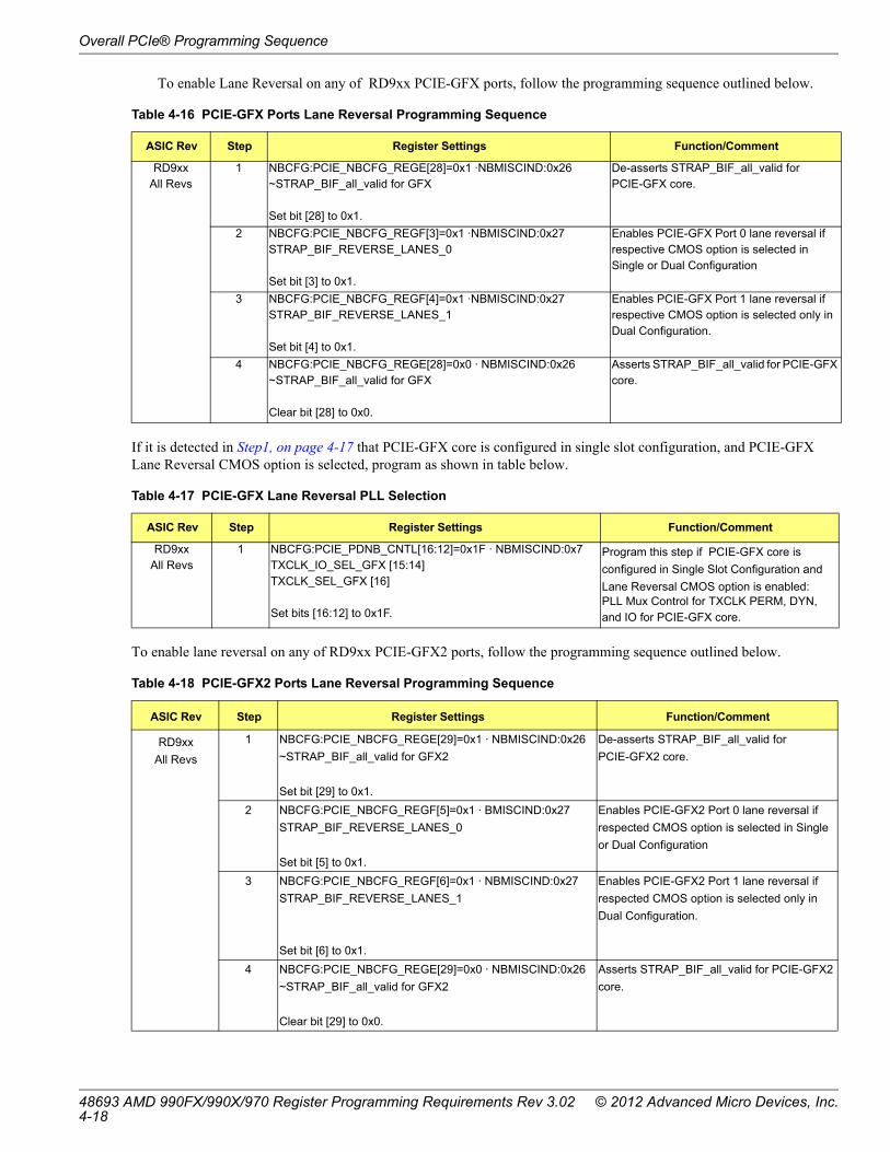
Overall PCIe® Programming Sequence
To enable Lane Reversal on any of RD9xx PCIE-GFX ports, follow the programming sequence outlined below.
If it is detected in Step1, on page 4-17 that PCIE-GFX core is configured in single slot configuration, and PCIE-GFX Lane Reversal CMOS option is selected, program as shown in table below.
To enable lane reversal on any of RD9xx PCIE-GFX2 ports, follow the programming sequence outlined below.
Table 4-16 PCIE-GFX Ports Lane Reversal Programming Sequence
ASIC Rev Step Register Settings Function/Comment
RD9xx All Revs
1 NBCFG:PCIE_NBCFG_REGE[28]=0x1 ·NBMISCIND:0x26~STRAP_BIF_all_valid for GFX
Set bit [28] to 0x1.
De-asserts STRAP_BIF_all_valid for PCIE-GFX core.
2 NBCFG:PCIE_NBCFG_REGF[3]=0x1 ·NBMISCIND:0x27 STRAP_BIF_REVERSE_LANES_0
Set bit [3] to 0x1.
Enables PCIE-GFX Port 0 lane reversal if respective CMOS option is selected in Single or Dual Configuration
3 NBCFG:PCIE_NBCFG_REGF[4]=0x1 ·NBMISCIND:0x27STRAP_BIF_REVERSE_LANES_1
Set bit [4] to 0x1.
Enables PCIE-GFX Port 1 lane reversal if respective CMOS option is selected only in Dual Configuration.
4 NBCFG:PCIE_NBCFG_REGE[28]=0x0 · NBMISCIND:0x26~STRAP_BIF_all_valid for GFX
Clear bit [28] to 0x0.
Asserts STRAP_BIF_all_valid for PCIE-GFX core.
Table 4-17 PCIE-GFX Lane Reversal PLL Selection
ASIC Rev Step Register Settings Function/Comment
RD9xx All Revs
1 NBCFG:PCIE_PDNB_CNTL[16:12]=0x1F · NBMISCIND:0x7 TXCLK_IO_SEL_GFX [15:14]TXCLK_SEL_GFX [16]
Set bits [16:12] to 0x1F.
Program this step if PCIE-GFX core is
configured in Single Slot Configuration and
Lane Reversal CMOS option is enabled:PLL Mux Control for TXCLK PERM, DYN, and IO for PCIE-GFX core.
Table 4-18 PCIE-GFX2 Ports Lane Reversal Programming Sequence
ASIC Rev Step Register Settings Function/Comment
RD9xx
All Revs
1 NBCFG:PCIE_NBCFG_REGE[29]=0x1 · NBMISCIND:0x26
~STRAP_BIF_all_valid for GFX2
Set bit [29] to 0x1.
De-asserts STRAP_BIF_all_valid for
PCIE-GFX2 core.
2 NBCFG:PCIE_NBCFG_REGF[5]=0x1 · BMISCIND:0x27
STRAP_BIF_REVERSE_LANES_0
Set bit [5] to 0x1.
Enables PCIE-GFX2 Port 0 lane reversal if
respected CMOS option is selected in Single
or Dual Configuration
3 NBCFG:PCIE_NBCFG_REGF[6]=0x1 · NBMISCIND:0x27
STRAP_BIF_REVERSE_LANES_1
Set bit [6] to 0x1.
Enables PCIE-GFX2 Port 1 lane reversal if
respected CMOS option is selected only in
Dual Configuration.
4 NBCFG:PCIE_NBCFG_REGE[29]=0x0 · NBMISCIND:0x26
~STRAP_BIF_all_valid for GFX2
Clear bit [29] to 0x0.
Asserts STRAP_BIF_all_valid for PCIE-GFX2
core.
48693 AMD 990FX/990X/970 Register Programming Requirements Rev 3.02 © 2012 Advanced Micro Devices, Inc.4-18

Overall PCIe® Programming Sequence
If it is detected in Step1, on page 4-17 that PCIE-GFX2 core is configured in single port configuration, and PCIE-GFX2 Lane Reversal CMOS option is selected, follow the sequence below.
To enable lane reversal on any of RD9xx PCIE-GPP ports, follow the programming sequence outlined below.
To enable lane reversal of the RD9xx PCIE-GPP2 port, follow the programming sequence outlined below.
Table 4-19 PCIE-GFX2 Lane Reversal PLL Selection
ASIC Rev Step Register Settings Function/Comment
RD9xx
All Revs
1 NBCFG:PCIE_PDNB_CNTL[23:20]=0x1F · NBMISCIND:0x7
NBCFG:PCIE_PDNB_CNTL[17]=0x1F · NBMISCIND:0x7
TXCLK_IO_SEL_GFX2 [23:22]
TXCLK_SEL_GFX2 [17]
Set bits [23:20] and [17] to 0x1F.
PLL Mux Control for TXCLK PERM, DYN, and IO
for PCIE-GFX2 core.
Table 4-20 PCIE-GPP Lane Reversal Programming Sequence
ASIC Rev Step Register Settings Function/Comment
RD9xxAll Revs
1 NBCFG:PCIE_NBCFG_REGE[30]=0x1 · NBMISCIND:0x26~STRAP_BIF_all_valid for PCIE-GPP
Set bit [30] to 0x1.
De-asserts STRAP_BIF_all_valid for PCIE-GPP core.
2 NBCFG:PCIE_NBCFG_REGF[7]=0x1 · NBMISCIND:0x27
STRAP_BIF_REVERSE_LANES_A_GPP
Set bit [7] to 0x1.
Enables PCIE-GPP Port 0 lane reversal if
respected CMOS option is selected.
3 NBCFG:PCIE_NBCFG_REGF[8]=0x1 · BMISCIND:0x27
STRAP_BIF_REVERSE_LANES_B_GPP
Set bit [8] to 0x1.
Enables PCIE-GPP Port 1 lane reversal if
respected CMOS option is selected.
4 NBCFG:PCIE_NBCFG_REGF[9]=0x1 · NBMISCIND:0x27
STRAP_BIF_REVERSE_LANES_C_GPP
Set bit [9] to 0x1.
Enables PCIE-GPP Port 2 lane reversal if
respected CMOS option is selected.
5 NBCFG:PCIE_NBCFG_REGE[30]=0x0 · NBMISCIND:0x26~STRAP_BIF_all_valid for PCIE-GPP
Clear bit [30] to 0x0.
Asserts STRAP_BIF_all_valid for PCIE-GPP core.
Table 4-21 PCIE-GPP2 Lane Reversal Programming Sequence
ASIC Rev Step Register Settings Function/Comment
RD9xxAll Revs
1 NBCFG:PCIE_NBCFG_REG15 [21]=0x1 · NBMISCIND:0x2D
~STRAP_BIF_all_valid for PCIE-GPP2
Set bit [21] to 0x1.
De-asserts STRAP_BIF_all_valid for
PCIE-GPP2 core.
2 NBCFG:PCIE_NBCFG_REG15 [25]=0x1 · NBMISCIND:0x2D
STRAP_BIF_REVERSE_LANES_A_GPP2
Set bit [25] to 0x1.
Enables PCIE-GPP2 Port 0 lane reversal if
respected CMOS option is selected in Single
or Dual Configuration
3 NBCFG:PCIE_NBCFG_REG15 [21]=0x0 · NBMISCIND:0x2D
~STRAP_BIF_all_valid for PCIE-GPP2
Clear bit [21] to 0x0.
Asserts STRAP_BIF_all_valid for PCIE-GPP2
core.
© 2012 Advanced Micro Devices, Inc. 48693 AMD 990FX/990X/970 Register Programming Requirements Rev 3.024-19

Overall PCIe® Programming Sequence
• Step 3: Complete PCIE-GFX, PCIE-GFX2 and PCIE-GPP Ports Configuration Programming:
If PCIE-GFX core is configured in dual slot configuration and none of the CMOS options in Step2, on page 4-17 are selected, then execute steps 6-8 of the programming sequence described in Table 4-3 “Programming Sequence for Loading Dual PCIE-GFX Core Configuration Topology” on page 4-8; otherwise, skip this step.
If PCIE-GFX2 core is configured in dual slot configuration, and none of the CMOS options in Step2, on page 4-17 are selected, then execute steps 6-8 of the programming sequence described in Table 4-4 “Programming Sequence for loading dual PCIE-GFX2 Core Configuration Topology” on page 4-9; otherwise, skip this step.
If "Pin Strap" method is used to configure PCIE-GPP core in order to reflect the required customer's system topology configuration, then program Line Director to distribute PCIe lanes across PCIe ports for the selected PCIE-GPP core configuration as indicated in Table 4-22 below.
If "Software Programming Sequence" is used instead, follow steps 4-6 specified in Table 4-12 “Switching PCIE-GPP Configurations” on page 4-13.
• Step 4: PCIE-GFX and PCIE-GFX2 Overclocking (CMOS Option – Disabled by Default):
RD9xx offers new overclocking capabilities which can maximize system performance at no extra hardware cost. Each RD9xx PCIE-GFX and PCIE-GFX2 PCIe cores can run at higher clock rates than their nominal factory rated speed.
Platforms tuned for optimal performance should have this CMOS option enabled by default.
The following CMOS options are available:
- Overclocking of PCIE-GFX core
- Overclocking of PCIE-GFX2 core
To enable overclocking of the RD9xx PCIE-GFX core, follow the programming sequence outlined below.
To enable overclocking of the RD9xx PCIE-GFX2 core, follow the programming sequence outlined below.
• Step 5: PCIe Global and Calibration Resets for PCIE-GFX and PCIE-GFX2 Cores:
Table 4-22 Programming PCIE-GGP Line Director
ASIC Rev Step Register Settings Function/Comment
RD9xxAll Revs
1 NBCFG:PCIE_NBCFG_REGE[27:0] · NBMISCIND:0x26
Program bits [27:0] to the value indicated in Table 4-13
“PCIE-GPP Line Director Mapping” on page 4-13
depending on PCIE-GGP configuration topology.
Program PCIE-GGP line director, depending on
chosen PCIE-GGP configuration topology. Refer
to Table 4-13 “PCIE-GPP Line Director Mapping”
on page 4-13 for mapping of programming value
to the PCIE-GGP configuration topology.
Table 4-23 PCIE-GFX PLL BW
ASIC Rev Step Register Settings Function/Comment
RD9xx All Revs
1 NBCFG:PCIE_NBCFG_REG3[9:0]=0xB5 · NBMISCIND:0x33B_P90PLL_IBIAS
Set bits [9:0] to 0xB5.
Increases PLL BW for 6G operation
Table 4-24 PCIE-GFX2 PLL BW
ASIC Rev Step Register Settings Function/Comment
RD9xxAll Revs
1 NBCFG:PCIE_NBCFG_REGA[9:0]=0xB5· NBMISCIND:0x22
B_P90PLL_IBIAS
Set bits [9:0] to 0xB5.
Increases PLL BW for 6G operation
48693 AMD 990FX/990X/970 Register Programming Requirements Rev 3.02 © 2012 Advanced Micro Devices, Inc.4-20

Overall PCIe® Programming Sequence
• Step 6: PCIe Ports Software Compliance (CMOS Option – Disabled by Default):
Characterization of PCIe transmitters requires placing them into compliance state which should not be entered in normal functional operation. The CMOS options below in Step6.1, on page 4-21 and Step6.2, on page 4-22 indicate programming sequences to force RD9xx PCIE-GFX, PCIE-GFX2, PCIE-GPP and PCIE-GPP2 ports transmitter into compliance state at Gen 1 or Gen 2 speed respectively.
• Step 6.1: PCIe Ports Gen1 Software Compliance (CMOS Option – Disabled by Default):
The PCIe Gen 1 Software Compliance feature is a function of a PCIe port. The following options are available:
• PCIE-GFX Port 0 Gen1 Software Compliance (Single/Dual Port Configuration)
• PCIE-GFX Port 1 Gen1 Software Compliance (Dual Port Configuration)
• PCIE-GFX2 Port 0 Gen1 Software Compliance (Single/Dual Port Configuration)
• PCIE-GFX2 Port 1 Gen1 Software Compliance (Dual Port Configuration)
• PCIE-GPP Port 0 Gen1 Software Compliance [NOTE: This CMOS option is applicable to the following PCIE-GPP configurations: 4:2:0:0:0:0, 4:1:1:0:0:0, 2:2:2:0:0:0, 2:2:1:1:0:0, 2:1:1:1:1:0, 1:1:1:1:1:1]
• PCIE-GPP Port 1 Gen1 Software Compliance [NOTE: This CMOS option is applicable to the following PCIE-GPP configurations: 4:2:0:0:0:0, 4:1:1:0:0:0, 2:2:2:0:0:0, 2:2:1:1:0:0, 2:1:1:1:1:0, 1:1:1:1:1:1]
• PCIE-GPP Port 2 Gen1 Software Compliance [NOTE: This CMOS option is applicable to the following PCIE-GPP configurations: 4:1:1:0:0:0, 2:2:2:0:0:0, 2:2:1:1:0:0, 2:1:1:1:1:0, 1:1:1:1:1:1]
Table 4-25 PCIE Global and Calibration Reset for PCIE-GFX and PCIE-GFX2 Cores Programming Sequence
ASIC Rev Step Register Settings Function/Comment
RD9xxAll Revs
1 NBCFG:PCIE_LINK_CFG [15:14]= 0x3 · NBMISCIND:0x8
CALIB_RESET_GFX
GLOBAL_RESET_GFX
Set bits [15:14] to 0x3.
Asserts both calibration reset and global
reset for PCIE-GFX core.
2 NBCFG:PCIE_LINK_CFG [13:12]= 0x3 · NBMISCIND:0x8
CALIB_RESET_GFX2
GLOBAL_RESET_GFX2
Set bits [13:12] to 0x3.
Asserts both calibration reset and global
reset for PCIE-GFX2 core.
3 NBCFG:PCIE_LINK_CFG [14]= 0x0 · NBMISCIND:0x8
CALIB_RESET_GFX
Clear bit[14] to 0x0.
De-asserts calibration reset for
PCIE-GFXcore.
4 NBCFG:PCIE_LINK_CFG [12]= 0x0 · NBMISCIND:0x8
CALIB_RESET_GFX2
Clear bit[12] to 0x0.
De-asserts calibration reset for
PCIE-GFX2core.
5 Wait for at least 200us
6 NBCFG:PCIE_LINK_CFG [15]= 0x0 · NBMISCIND:0x8
CALIB_RESET_GFX
Clear bit [15] to 0x0.
De-asserts global reset for
PCIE-GFXcore.
7 NBCFG:PCIE_LINK_CFG [13]= 0x0 · NBMISCIND:0x8
CALIB_RESET_GFX2
Clear bit [13] to 0x0.
De-asserts global reset for PCIE-GFX2
core.
© 2012 Advanced Micro Devices, Inc. 48693 AMD 990FX/990X/970 Register Programming Requirements Rev 3.024-21

Overall PCIe® Programming Sequence
• PCIE-GPP Port 3 Gen1 Software Compliance [NOTE: This CMOS option is applicable to the following PCIE-GPP configurations: 2:2:1:1:0:0, 2:1:1:1:1:0, 1:1:1:1:1:1]
• PCIE-GPP Port 4 Gen1 Software Compliance [NOTE: This CMOS option is applicable to the following PCIE-GPP configurations:2:1:1:1:1:0, 1:1:1:1:1:1]
• PCIE-GPP Port 5 Gen1 Software Compliance [NOTE: This CMOS option is applicable to the following PCIE-GPP configuration: 1:1:1:1:1:1]
• PCIE-GPP2 Port 0 Gen1 Software Compliance
To initiate PCIe Gen1 Software Compliance for each of the options listed above, follow the programming sequence below.
• Step 6.2: PCIe Ports Gen2 Software Compliance (CMOS Option – Disabled by Default):
The PCIe Gen2 Software Compliance feature is a function of a PCIe port.
The following options are available:
• PCIE-GFX Port 0 Gen2 Software Compliance (Single/Dual Port Configuration)
• PCIE-GFX Port 1 Gen2 Software Compliance (Dual Port Configuration)
• PCIE-GFX2 Port 0 Gen2 Software Compliance (Single/Dual Port Configuration)
• PCIE-GFX2 Port 1 Gen2 Software Compliance (Dual Port Configuration)
• PCIE-GPP Port 0 Gen2 Software Compliance [NOTE: This CMOS option is applicable to the following PCIE-GPP configurations: 4:2:0:0:0:0, 4:1:1:0:0:0, 2:2:2:0:0:0, 2:2:1:1:0:0, 2:1:1:1:1:0, 1:1:1:1:1:1]
• PCIE-GPP Port 1 Gen2 Software Compliance [NOTE: This CMOS option is applicable to the following PCIE-GPP configurations: 4:2:0:0:0:0, 4:1:1:0:0:0, 2:2:2:0:0:0, 2:2:1:1:0:0, 2:1:1:1:1:0, 1:1:1:1:1:1]
• PCIE-GPP Port 2 Gen2 Software Compliance [NOTE: This CMOS option is applicable to the following PCIE-GPP configurations: 4:1:1:0:0:0, 2:2:2:0:0:0, 2:2:1:1:0:0, 2:1:1:1:1:0, 1:1:1:1:1:1]
• PCIE-GPP Port 3 Gen2 Software Compliance [NOTE: This CMOS option is applicable to the following PCIE-GPP configurations: 2:2:1:1:0:0, 2:1:1:1:1:0, 1:1:1:1:1:1]
• PCIE-GPP Port 4 Gen2 Software Compliance [NOTE: This CMOS option is applicable to the following PCIE-GPP configurations:2:1:1:1:1:0, 1:1:1:1:1:1]
• PCIE-GPP Port 5 Gen2 Software Compliance [NOTE: This CMOS option is applicable to the following PCIE-GPP configuration: 1:1:1:1:1:1]
• PCIE-GPP2 Port 0 Gen2 Software Compliance
Table 4-26 PCIe Gen1 Software Compliance Programming Sequence
ASIC Rev Step Register Settings Function/Comment
RD9xx All Revs
1 BIF_NBP:PCIEP_STRAP_LC [13]=0x1 · PCIEIND_P:0xC0
STRAP_FORCE_COMPLIANCE
Set bit [13] to 0x1.
Forces root-complex transmitter to output
compliance pattern at Gen1 rate.
48693 AMD 990FX/990X/970 Register Programming Requirements Rev 3.02 © 2012 Advanced Micro Devices, Inc.4-22

Overall PCIe® Programming Sequence
To initiate PCIe Gen2 Software Compliance for each of the options listed above, follow the programming sequence below.
• Step 7: Programming PCIe Cores PHY for Per Link Channel Characteristics
[NOTE: RD9xx has Transmitter Drive Strength, Half-Swing, Zero De-Emphasis controls implemented on per core basis, rather than per port basis. This should be taken into consideration when defining system configuration topology.]
Each RD9xx PCIe channel is defined by its insertion loss, return loss and aggressor-victim coupling. Understanding and managing the amount of signal attenuation that can be tolerated between the transmitter and receiver of each PCIe link is critical for proper system functionality. There are many factors contributing to the channel loss of a PCIe link, such as the number of PCB layers, shape and length of each microstrip and stripline which define its inductive and capacitive characteristics, PCB characteristics (material, thickness etc.), platform form factor, etc. Loading these parameters into simulation environment on multiple RD9xx platforms has resulted in identifying three major types of channels. For each of these channel types, it is recommended to configure PCIE PHY parameters as indicated below. These categories can be used as starting points for additional fine tuning if necessary for particular platform implementations.
• Short Channels (less than 3” in length)
Short channels, typically present on compact platforms, should be optimized for maximum power savings and hence RD9xx PCIe ports should have their transmitters operating in half-swing, zero de-emphasis signaling mode. To set RD9xx PCIE-GFX, PCIE-GFX2, PCIE-SB, PCIE-GPP and PCIE-GPP2 PCIe transmitters for half-swing, zero-de-emphasis signaling, follow Step7.1: ”Half Swing, Zero De-emphasis (CMOS option)” on page 4-24.
• Medium Channels (between 3” and 12” in length)
Medium channels are deployed on most platforms. Transmitters’ drive strength of RD9xx PCIE-GFX, PCIE-GFX2, PCIE-SB, PCIE-GPP and PCIE-GPP2 PCIe ports should be set to 22mA when operating in either Gen 1 or Gen 2 link speeds. Step7.2: ”Transmitter Drive Strength (CMOS Option)” on page 4-25 should be followed for programming sequence. Root complex should set de-emphasis value of PCIE-GFX, PCIE-GFX2, PCIE-SB, PCIE-GPP and PCIE-GPP2 PCIe transmitters to -3.5dB when operating in either Gen 1 or Gen 2 speeds as well as advertise required -3.5dB de-emphasis setting of endpoint transmitters when operating in Gen 2 speed, to the Gen 2 compliant endpoint device during link training. This PCIe PHY setting is the default setting after a power-on reset or a warm-reset event, so no programming is required.
• Long Channels (more than 12” in length)
In long channels, transmitter’s drive strength of RD9xx PCIE-GFX, PCIE-GFX2, PCIE-SB, PCIE-GPP and PCIE-GPP2 PCIe ports should be set to 26mA when operating in either Gen 1 or Gen 2 link speeds. Root complex should set de-emphasis value of the PCIE-GFX, PCIE-GFX2, PCIE-SB, PCIE-GPP and PCIE-GPP2 transmitters to -3.5dB when operating in Gen 1 link speed and -6dB when operating in Gen 2 link speed as well as advertise required -6dB de-emphasis setting of endpoint transmitters when operating in Gen 2 speed, to the Gen 2 compliant endpoint device during link training. To configure RD9xx PCIE-GFX, PCIE-GFX2, PCIE-SB, PCIE-GPP and PCIE-GPP2 PCIe PHY transmitter with these parameters, follow Step7.2: ”Transmitter Drive Strength (CMOS Option)” on page 4-25 and Step7.3: ”Configured and RC Advertised De-emphasis Strength (CMOS Option)” on page 4-26.
Table 4-27 PCIe Gen2 Software Compliance Programming Sequence
ASIC Rev Step Register Setting Function/Comment
RD9xx All Revs
1 BIF_NBP:PCIE_LC_SPEED_CNTL[0]=0x1 · PCIEIND_P:0xA4 LC_GEN2_EN_STRAP
Set bit [0] to 0x1.
Enables Gen 2 capability of root complex port *
2 BIF_NBP:LINK_CNTL2[3:0]=0x2 · pcieCopcieConfigDev*:0x88TARGET_LINK_SPEED
Set bits [3:0] to 0x2.
Advertises root complex port * link speed to be Gen2
3 BIF_NBP:LINK_CNTL2[4]=0x1 · pcieCopcieConfigDev*:0x88ENTER_COMPLIANCE
Set bit [4] to 0x1.
Forces root complex port * transmitter to enter Compliance mode at Gen2 rate.
© 2012 Advanced Micro Devices, Inc. 48693 AMD 990FX/990X/970 Register Programming Requirements Rev 3.024-23

Overall PCIe® Programming Sequence
• Step 7.1: Half Swing, Zero De-emphasis (CMOS option)
The following CMOS options are available:
• Half Swing, Zero De-Emphasis for PCIE-GFX Transmitters
• Half Swing, Zero De-Emphasis for PCIE-GFX2 Transmitters
• Half Swing, Zero De-Emphasis for PCIE-SB Transmitters
• Half Swing, Zero De-Emphasis for PCIE-GPP Transmitters
• Half Swing, Zero De-Emphasis for PCIE-GPP2 Transmitters
To set RD9xx PCIE-GFX, PCIE-GFX2, PCIE-SB, PCIE-GPP and PCIE-GPP2PCIe transmitters for half-swing, zero-de-emphasis signaling, follow the programming sequence below.
Table 4-28 Half Swing, Zero De-emphasis for PCIE-GFX, PCIE-GFX2, PCIE-SB, PCIE-GPP and PCIE-GPP2 Transmitters
ASIC Rev Step Register Settings Function/Comment
RD9xx All Revs
1 Half-Swing for all PCIE-GFX Transmitters:NBCFG:PCIE_NBCFG_REG5[18]=0x0 · NBMISCIND:0x35 B_PTX_PWRS_ENB_GFX
Clear bit [18] to 0x0.
Zero De-Emphases for all PCIE-GFX Transmitters:NBCFG:PCIE_NBCFG_REG6[25:24]=0x0 · NBMISCIND:0x36 B_PTX_DEEMPH_EN_GFXClear bits [25:24] to 0x0.
Half Swing, Zero De-emphasis for all PCIE-GFX Transmitters.
2 Half-Swing for all PCIE-GFX2 Transmitters:NBCFG:PCIE_NBCFG_REG5[19]=0x0 · NBMISCIND:0x35 B_PTX_PWRS_ENB_GFX2
Clear bit [19] to 0x0.
Zero De-Emphases for all PCIE-GFX Transmitters:NBCFG:PCIE_NBCFG_REG6[27:26]=0x0 · NBMISCIND:0x36 B_PTX_DEEMPH_EN_GFX2
Clear bits [27:26] to 0x0.
Half Swing, Zero De-emphasis for all PCIE-GFX2 Transmitters.
3 Half-Swing for all PCIE-SB Transmitters:NBCFG:StrapsOutputMux_7[27]=0x0 · NBMISCIND:0x67 B_PTX_PWRS_ENB_SBClear bit [27] to 0x0.
Zero De-Emphases for all PCIE-SB Transmitters:NBCFG:StrapsOutputMux_8[21:20]=0x0 · NBMISCIND:0x68 B_PTX_DEEMPH_EN_sb
Clear bits [21:20] to 0x0.
Half Swing, Zero De-emphasis for all PCIE-SB Transmitters.
4 Half-Swing for all PCIE-GPP Transmitters:NBCFG:PCIE_NBCFG_REG5[20]=0x0 · NBMISCIND:0x35 B_PTX_PWRS_ENB_GPPClear bit [20] to 0x0.
Zero De-Emphases for all PCIE-GPP Transmitters:NBCFG:PCIE_NBCFG_REG6[29:28]=0x0 · NBMISCIND:0x36 B_PTX_DEEMPH_EN_GPP
Clear bits [29:28] to 0x0.
Half Swing, Zero De-emphasis for all PCIE-GPP Transmitters.
48693 AMD 990FX/990X/970 Register Programming Requirements Rev 3.02 © 2012 Advanced Micro Devices, Inc.4-24

Overall PCIe® Programming Sequence
• Step 7.2: Transmitter Drive Strength (CMOS Option)
The following CMOS options are available:
• Transmitter Drive Strength for PCIE-GFX Core
• Transmitter Drive Strength for PCIE-GFX2 Core
• Transmitter Drive Strength for PCIE-SB Core
• Transmitter Drive Strength for PCIE-GPP Core
• Transmitter Drive Strength for PCIE-GPP2 Core
To set transmitter drive strength on RD9xx PCIE-GFX, PCIE-GFX2, PCIE-SB, PCIE-GPP and PCIE-GPP2 PCIe ports, follow the programming sequence below.
RD9xx All Revs
5 Half-Swing for all PCIE-GPP2 Transmitters:NBCFG:PCIE_NBCFG_REG14[2]=0x0 · NBMISCIND:0x2C B_PTX_PWRS_ENB_GPP2Clear bit [2] to 0x0.
Zero De-Emphases for all PCIE-GPP2 Transmitters:NBCFG:PCIE_NBCFG_REG13[11:10]=0x0 · NBMISCIND:0x2B B_PTX_DEEMPH_EN_GPP2
Clear bits [11:10] to 0x0.
Half Swing, Zero De-emphasis for all PCIE-GPP2 Transmitters.
Table 4-29 Transmitter Drive Strength for PCIE-GFX, PCIE-GFX2, PCIE-SB, PCIE-GPP and PCIE-GPP2Transmitters
ASIC Rev Step Register Settings Function/Comment
RD9xx
All Revs
1 Transmitter Drive Strength for all PCIE-GFX Transmitters:
NBCFG:PCIE_NBCFG_REG5 [27:26] · NBMISCIND:0x35
B_P90TX_DRV_STR[1:0] for GFX
Set bits [27:26] according to the CMOS option selected.
Transmitter Drive Strength for all PCIE-GFX
Transmitters in both Gen 1 and Gen 2 link speeds:
Possible CMOS options:
0x0: 26mA nominal
0x1: 20mA nominal
0x2: 22mA nominal
0x3: 24mA nominal
To give better signal integrity for PCIe lanes
program [27:26] according to the CMOS option
selected.
2 Transmitter Drive Strength for all PCIE-GFX2 Transmitters:
NBCFG:PCIE_NBCFG_REG5 [29:28] · NBMISCIND:0x35
B_P90TX_DRV_STR[1:0] for GFX2
Set bits [27:26] according to the CMOS option selected.
Transmitter Drive Strength for all PCIE-GFX2
Transmitters in both Gen 1 and Gen 2 link speeds:
Possible CMOS options:
0x0: 26mA nominal
0x1: 20mA nominal
0x2: 22mA nominal
0x3: 24mA nominal
To give better signal integrity for PCIe lanes
program [29:28] according to the CMOS option
selected.
Table 4-28 Half Swing, Zero De-emphasis for PCIE-GFX, PCIE-GFX2, PCIE-SB, PCIE-GPP and PCIE-GPP2 Transmitters (Continued)
ASIC Rev Step Register Settings Function/Comment
© 2012 Advanced Micro Devices, Inc. 48693 AMD 990FX/990X/970 Register Programming Requirements Rev 3.024-25
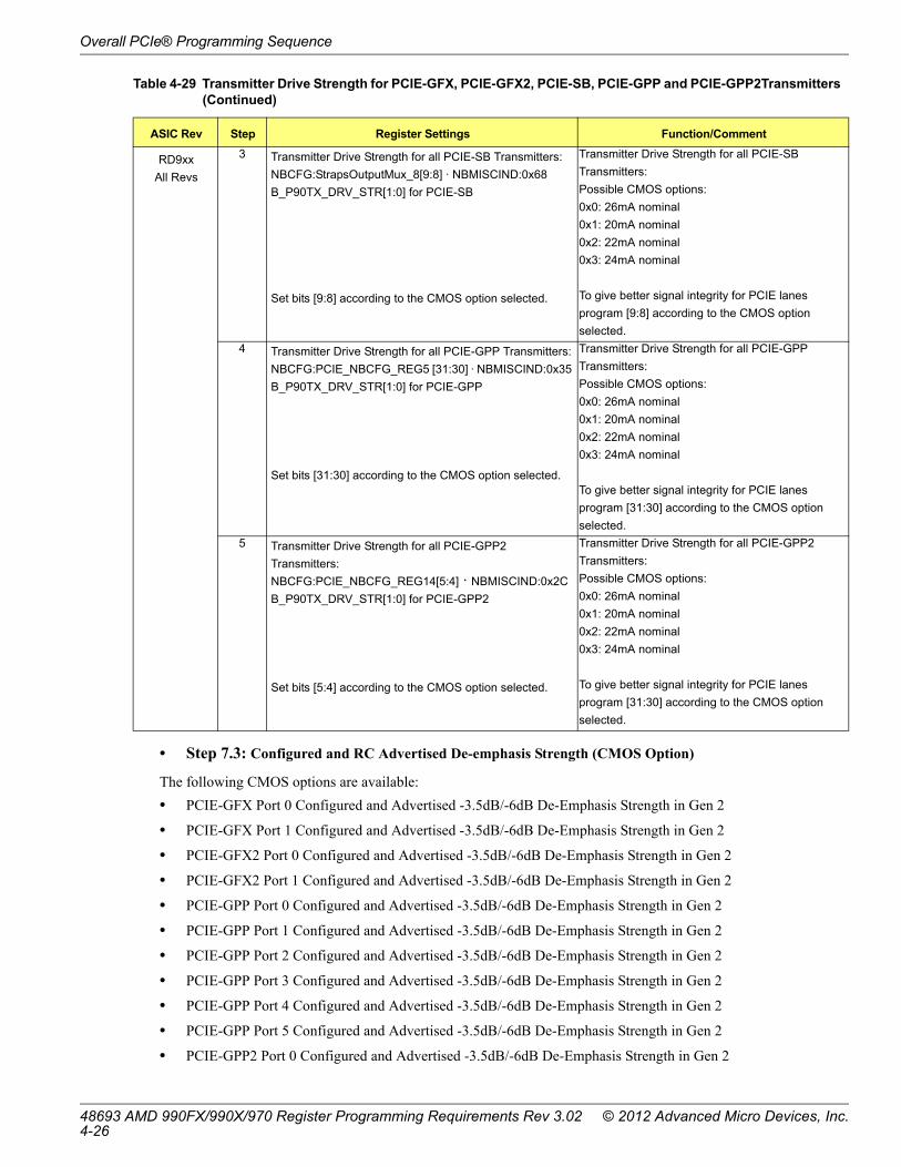
Overall PCIe® Programming Sequence
• Step 7.3: Configured and RC Advertised De-emphasis Strength (CMOS Option)
The following CMOS options are available:
• PCIE-GFX Port 0 Configured and Advertised -3.5dB/-6dB De-Emphasis Strength in Gen 2
• PCIE-GFX Port 1 Configured and Advertised -3.5dB/-6dB De-Emphasis Strength in Gen 2
• PCIE-GFX2 Port 0 Configured and Advertised -3.5dB/-6dB De-Emphasis Strength in Gen 2
• PCIE-GFX2 Port 1 Configured and Advertised -3.5dB/-6dB De-Emphasis Strength in Gen 2
• PCIE-GPP Port 0 Configured and Advertised -3.5dB/-6dB De-Emphasis Strength in Gen 2
• PCIE-GPP Port 1 Configured and Advertised -3.5dB/-6dB De-Emphasis Strength in Gen 2
• PCIE-GPP Port 2 Configured and Advertised -3.5dB/-6dB De-Emphasis Strength in Gen 2
• PCIE-GPP Port 3 Configured and Advertised -3.5dB/-6dB De-Emphasis Strength in Gen 2
• PCIE-GPP Port 4 Configured and Advertised -3.5dB/-6dB De-Emphasis Strength in Gen 2
• PCIE-GPP Port 5 Configured and Advertised -3.5dB/-6dB De-Emphasis Strength in Gen 2
• PCIE-GPP2 Port 0 Configured and Advertised -3.5dB/-6dB De-Emphasis Strength in Gen 2
RD9xx
All Revs
3 Transmitter Drive Strength for all PCIE-SB Transmitters:
NBCFG:StrapsOutputMux_8[9:8] · NBMISCIND:0x68
B_P90TX_DRV_STR[1:0] for PCIE-SB
Set bits [9:8] according to the CMOS option selected.
Transmitter Drive Strength for all PCIE-SB
Transmitters:
Possible CMOS options:
0x0: 26mA nominal
0x1: 20mA nominal
0x2: 22mA nominal
0x3: 24mA nominal
To give better signal integrity for PCIE lanes
program [9:8] according to the CMOS option
selected.
4 Transmitter Drive Strength for all PCIE-GPP Transmitters:
NBCFG:PCIE_NBCFG_REG5 [31:30] · NBMISCIND:0x35
B_P90TX_DRV_STR[1:0] for PCIE-GPP
Set bits [31:30] according to the CMOS option selected.
Transmitter Drive Strength for all PCIE-GPP
Transmitters:
Possible CMOS options:
0x0: 26mA nominal
0x1: 20mA nominal
0x2: 22mA nominal
0x3: 24mA nominal
To give better signal integrity for PCIE lanes
program [31:30] according to the CMOS option
selected.
5 Transmitter Drive Strength for all PCIE-GPP2
Transmitters:
NBCFG:PCIE_NBCFG_REG14[5:4] · NBMISCIND:0x2C
B_P90TX_DRV_STR[1:0] for PCIE-GPP2
Set bits [5:4] according to the CMOS option selected.
Transmitter Drive Strength for all PCIE-GPP2
Transmitters:
Possible CMOS options:
0x0: 26mA nominal
0x1: 20mA nominal
0x2: 22mA nominal
0x3: 24mA nominal
To give better signal integrity for PCIE lanes
program [31:30] according to the CMOS option
selected.
Table 4-29 Transmitter Drive Strength for PCIE-GFX, PCIE-GFX2, PCIE-SB, PCIE-GPP and PCIE-GPP2Transmitters (Continued)
ASIC Rev Step Register Settings Function/Comment
48693 AMD 990FX/990X/970 Register Programming Requirements Rev 3.02 © 2012 Advanced Micro Devices, Inc.4-26
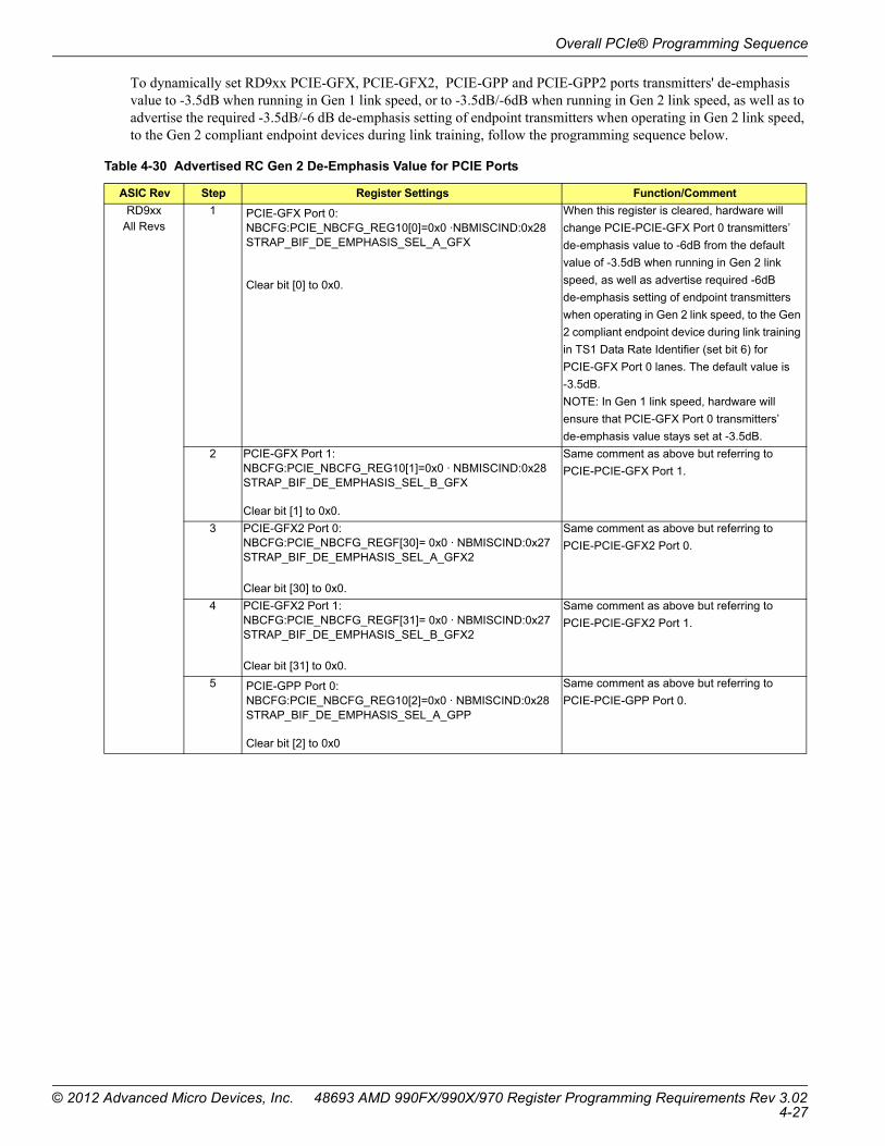
Overall PCIe® Programming Sequence
To dynamically set RD9xx PCIE-GFX, PCIE-GFX2, PCIE-GPP and PCIE-GPP2 ports transmitters' de-emphasis value to -3.5dB when running in Gen 1 link speed, or to -3.5dB/-6dB when running in Gen 2 link speed, as well as to advertise the required -3.5dB/-6 dB de-emphasis setting of endpoint transmitters when operating in Gen 2 link speed, to the Gen 2 compliant endpoint devices during link training, follow the programming sequence below.
Table 4-30 Advertised RC Gen 2 De-Emphasis Value for PCIE Ports
ASIC Rev Step Register Settings Function/Comment
RD9xx All Revs
1 PCIE-GFX Port 0:NBCFG:PCIE_NBCFG_REG10[0]=0x0 ·NBMISCIND:0x28STRAP_BIF_DE_EMPHASIS_SEL_A_GFX
Clear bit [0] to 0x0.
When this register is cleared, hardware will
change PCIE-PCIE-GFX Port 0 transmitters’
de-emphasis value to -6dB from the default
value of -3.5dB when running in Gen 2 link
speed, as well as advertise required -6dB
de-emphasis setting of endpoint transmitters
when operating in Gen 2 link speed, to the Gen
2 compliant endpoint device during link training
in TS1 Data Rate Identifier (set bit 6) for
PCIE-GFX Port 0 lanes. The default value is
-3.5dB.
NOTE: In Gen 1 link speed, hardware will
ensure that PCIE-GFX Port 0 transmitters’
de-emphasis value stays set at -3.5dB.
2 PCIE-GFX Port 1:NBCFG:PCIE_NBCFG_REG10[1]=0x0 · NBMISCIND:0x28 STRAP_BIF_DE_EMPHASIS_SEL_B_GFX
Clear bit [1] to 0x0.
Same comment as above but referring to
PCIE-PCIE-GFX Port 1.
3 PCIE-GFX2 Port 0:NBCFG:PCIE_NBCFG_REGF[30]= 0x0 · NBMISCIND:0x27STRAP_BIF_DE_EMPHASIS_SEL_A_GFX2
Clear bit [30] to 0x0.
Same comment as above but referring to
PCIE-PCIE-GFX2 Port 0.
4 PCIE-GFX2 Port 1:NBCFG:PCIE_NBCFG_REGF[31]= 0x0 · NBMISCIND:0x27STRAP_BIF_DE_EMPHASIS_SEL_B_GFX2
Clear bit [31] to 0x0.
Same comment as above but referring to
PCIE-PCIE-GFX2 Port 1.
5 PCIE-GPP Port 0:NBCFG:PCIE_NBCFG_REG10[2]=0x0 · NBMISCIND:0x28 STRAP_BIF_DE_EMPHASIS_SEL_A_GPP
Clear bit [2] to 0x0
Same comment as above but referring to
PCIE-PCIE-GPP Port 0.
© 2012 Advanced Micro Devices, Inc. 48693 AMD 990FX/990X/970 Register Programming Requirements Rev 3.024-27

Overall PCIe® Programming Sequence
• Step 8: Program Optimal PCIe Cores PHY Parameters
To set optimal RD9xx PCIe cores PCIe PHY parameters, follow the programming sequence below.
RD9xx All Revs
6 PCIE-GPP Port 1:NBCFG:PCIE_NBCFG_REG10[3]=0x0 · NBMISCIND:0x28 STRAP_BIF_DE_EMPHASIS_SEL_B_GPP
Clear bit [3] to 0x0
Same comment as above but referring to
PCIE-PCIE-GPP Port 1.
7 PCIE-GPP Port 2:NBCFG:PCIE_NBCFG_REG10[4]=0x0 · NBMISCIND:0x28 STRAP_BIF_DE_EMPHASIS_SEL_C_GPP
Clear bit [4] to 0x0
Same comment as above but referring to
PCIE-PCIE-GPP Port 2.
8 PCIE-GPP Port 3:NBCFG:PCIE_NBCFG_REG10[5]=0x0 · NBMISCIND:0x28 STRAP_BIF_DE_EMPHASIS_SEL_D_GPP
Clear bit [5] to 0x0
Same comment as above but referring to
PCIE-PCIE-GPP Port 3.
9 PCIE-GPP Port 4:NBCFG:PCIE_NBCFG_REG10[6]=0x0 · NBMISCIND:0x28 STRAP_BIF_DE_EMPHASIS_SEL_E_GPPa
Clear bit [5] to 0x0
Same comment as above but referring to
PCIE-PCIE-GPP Port 4.
10 PCIE-GPP Port 5:NBCFG:PCIE_NBCFG_REG10[7]=0x0 · NBMISCIND:0x28 STRAP_BIF_DE_EMPHASIS_SEL_F_GPP
Clear bit [7] to 0x0.
Same comment as above but referring to
PCIE-PCIE-GPP Port 5.
11 PCIE-GPP2 Port 0:NBCFG:PCIE_NBCFG_REG15[5] =0x0 · NBMISCIND:0x2D STRAP_BIF_DE_EMPHASIS_SEL_A_GPP2
Clear bit [5] to 0x0.
Same comment as above but referring to
PCIE-PCIE-GPP2 Port 0.
Table 4-31 Optimal PCIe Cores PHY Parameters
ASIC Rev Step Register Settings Function/Comment
RD9xxAll Revs
1 PCIE-GFX Phase Filter size:NBCFG:PCIE_NBCFG_REG8[7:6]=0x3 · NBMISCIND:0x38
B_P90RX_CRFR_ON_GFXSet bits [7:6] to 0x3.
NBCFG:PCIE_NBCFG_REG4[7]=0x0 · NBMISCIND:0x34
B_P90PLL_BACKUP_2_GFXClear bit [7] to 0x0.
NBCFG:PCIE_NBCFG_REG7[23:20]=0xD · NBMISCIND:0x37
B_P90RX_CRPHSIZE_GFXSet bits [23:20] to 0xD.
CDR Phase Filter Size for BW control of PCIE-GFX core.
Table 4-30 Advertised RC Gen 2 De-Emphasis Value for PCIE Ports (Continued)
ASIC Rev Step Register Settings Function/Comment
48693 AMD 990FX/990X/970 Register Programming Requirements Rev 3.02 © 2012 Advanced Micro Devices, Inc.4-28
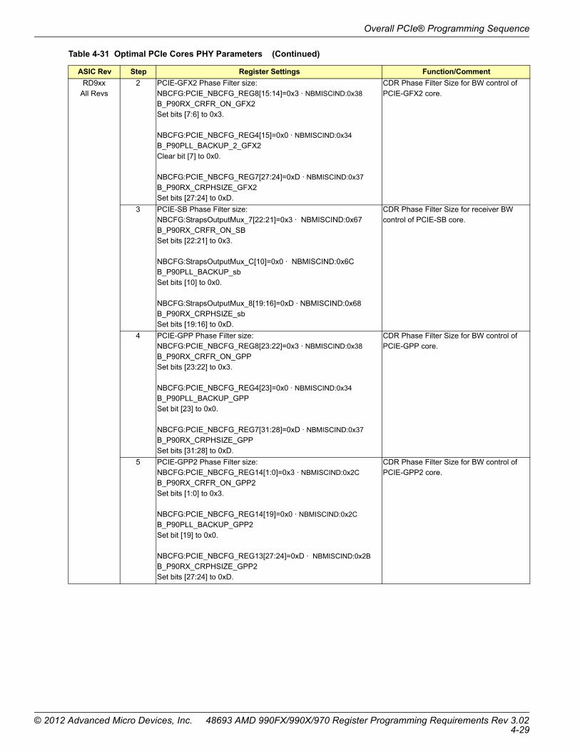
Overall PCIe® Programming Sequence
RD9xxAll Revs
2 PCIE-GFX2 Phase Filter size:NBCFG:PCIE_NBCFG_REG8[15:14]=0x3 · NBMISCIND:0x38
B_P90RX_CRFR_ON_GFX2Set bits [7:6] to 0x3.
NBCFG:PCIE_NBCFG_REG4[15]=0x0 · NBMISCIND:0x34
B_P90PLL_BACKUP_2_GFX2Clear bit [7] to 0x0.
NBCFG:PCIE_NBCFG_REG7[27:24]=0xD · NBMISCIND:0x37
B_P90RX_CRPHSIZE_GFX2Set bits [27:24] to 0xD.
CDR Phase Filter Size for BW control of PCIE-GFX2 core.
3 PCIE-SB Phase Filter size:NBCFG:StrapsOutputMux_7[22:21]=0x3 · NBMISCIND:0x67 B_P90RX_CRFR_ON_SBSet bits [22:21] to 0x3.
NBCFG:StrapsOutputMux_C[10]=0x0 · NBMISCIND:0x6C B_P90PLL_BACKUP_sbSet bits [10] to 0x0.
NBCFG:StrapsOutputMux_8[19:16]=0xD · NBMISCIND:0x68 B_P90RX_CRPHSIZE_sbSet bits [19:16] to 0xD.
CDR Phase Filter Size for receiver BW control of PCIE-SB core.
4 PCIE-GPP Phase Filter size:NBCFG:PCIE_NBCFG_REG8[23:22]=0x3 · NBMISCIND:0x38
B_P90RX_CRFR_ON_GPPSet bits [23:22] to 0x3.
NBCFG:PCIE_NBCFG_REG4[23]=0x0 · NBMISCIND:0x34
B_P90PLL_BACKUP_GPPSet bit [23] to 0x0.
NBCFG:PCIE_NBCFG_REG7[31:28]=0xD · NBMISCIND:0x37
B_P90RX_CRPHSIZE_GPPSet bits [31:28] to 0xD.
CDR Phase Filter Size for BW control of PCIE-GPP core.
5 PCIE-GPP2 Phase Filter size:NBCFG:PCIE_NBCFG_REG14[1:0]=0x3 · NBMISCIND:0x2C
B_P90RX_CRFR_ON_GPP2Set bits [1:0] to 0x3.
NBCFG:PCIE_NBCFG_REG14[19]=0x0 · NBMISCIND:0x2C
B_P90PLL_BACKUP_GPP2Set bit [19] to 0x0.
NBCFG:PCIE_NBCFG_REG13[27:24]=0xD · NBMISCIND:0x2B
B_P90RX_CRPHSIZE_GPP2Set bits [27:24] to 0xD.
CDR Phase Filter Size for BW control of PCIE-GPP2 core.
Table 4-31 Optimal PCIe Cores PHY Parameters (Continued)
ASIC Rev Step Register Settings Function/Comment
© 2012 Advanced Micro Devices, Inc. 48693 AMD 990FX/990X/970 Register Programming Requirements Rev 3.024-29

Overall PCIe® Programming Sequence
RD9xxAll Revs
6 NBCFG:PCIE_NBCFG_REG2[21:20]=0x2 · NBMISCIND:0x32 B_PG2PLL_IDLEDET_TH[1:0] for PCIE-GFXSet bits [21:20] to 0x2.
NBCFG:PCIE_NBCFG_REG2[23:22]= 0x2 · NBMISCIND: 0x32 B_PG2PLL_IDLEDET_TH[1:0] for PCIE-GFX2Set bits [23:22] to 0x2.
NBCFG:StrapsOutputMux_7[11:10]=0x2 · NBMISCIND:0x67B_PG2PLL_IDLEDET_TH[1:0] for SB.Set bits [11:20] to 0x2.
NBCFG:PCIE_NBCFG_REG2[25:24]=0x2 · NBMISCIND:0x32 B_PG2PLL_IDLEDET_TH[1:0] for GPPSet bits [25:24] to 0x2.
NBCFG:PCIE_NBCFG_REG12[17:16]=0x2 · NBMISCIND:0x2AB_PG2PLL_IDLEDET_TH[17:16] for GPP2Set bits [17:16] to 0x2.
Sets threshold for Electrical Idle Detector circuit.
7 NBCFG:StrapsOutputMux_B[30: 29]=0x3 · NBMISCIND:0x6B B_P90RX_INCAL_FORCE_GFXB_P90RX_INCAL_FORCE_GFX2Set bits [30:29] to 0x3.
NBCFG:StrapsOutputMux_B[28]=0x1 · NBMISCIND:0x6B B_P90RX_INCAL_FORCE_sb Set bit [28] to 0x1.
NBCFG:StrapsOutputMux_B[31]=0x1 · NBMISCIND:0x6BB_P90RX_INCAL_FORCE_GPPSet bit [31] to 0x1.
NBCFG:StrapsOutputMux_B[27]=0x1 · NBMISCIND:0x6B
B_P90RX_INCAL_FORCE_GPP2 Set bit [27] to 0x1.
Turn off Offset Cancellation circuit.
8 NBCFG:PCIE_NBCFG_REG7[12:11]=0x0 · NBMISCIND:0x37 B_P90RX_CLKG_EN_GFXB_P90RX_CLKG_EN_GFX2
Clear bits [12:11] to 0x0.
NBCFG:StrapsOutputMux_7[26]=0x0 · NBMISCIND:0x67 B_P90RX_CLKG_EN_SBClear bit [26] to 0x0.
NBCFG:PCIE_NBCFG_REG7[13]=0x0 · NBMISCIND:0x37 B_P90RX_CLKG_EN_GPPClear bit [13] to 0x0.
NBCFG:PCIE_NBCFG_REG14[10]=0x0 · NBMISCIND:0x2CB_P90RX_CLKG_EN_GPP2Clear bit [10] to 0x0.
Disables Rx Clock gating in CDR circuit.
9 BIF_NBP:PCIE_LC_CNTL2[28]=0x1·PCIEIND_P:0xB1LC_ENABLE_RX_CR_EN_DEASSERTION
Set bit [28] to 0x1.
Enables de-assertion of PG2RX_CR_EN to lock clock recovery parameter when lane is in electrical idle in L0s.
Table 4-31 Optimal PCIe Cores PHY Parameters (Continued)
ASIC Rev Step Register Settings Function/Comment
48693 AMD 990FX/990X/970 Register Programming Requirements Rev 3.02 © 2012 Advanced Micro Devices, Inc.4-30

Overall PCIe® Programming Sequence
• Step 9: System BIOS Compile Flags
SBIOS needs to provide Compile Flags to bypass the training sequence for unsupported PCIe devices. When the training is bypassed, the corresponding port should be powered down as well.
• Step 10: Releasing Resets for PCIe Links (CMOS Option - Enabled by Default)
RD9xx has a number of software controllable GPIOs which can be used to control resets to endpoint devices. End-point devices can be connected to RD9xx PCIe ports either via PCIe slot (standard, hot-plug implemented slot etc…) or can be directly mounted on the platform. Each hot-plug implemented slot should have a dedicated software controllable GPIO to control reset to the slot, while non-hot-plug PCIe links can share one or more software controllable GPIOs. The most flexible and hence most desirable platform solution would ideally have each PCIe link reset independently controlled.
Available RD9xx software controllable GPIOs to control resets to PCIe slots are: PCIE_RESET_GPIO1, PCIE_RESET_GPIO2, PCIE_RESET_GPIO4, PCIE_RESET_GPIO5. Additional software controllable GPIOs to control resets to PCIe slots can be derived from a number of other places on a platform such as Super IOs, South Bridge etc.
If RD9xx software controllable GPIOs are used to control reset of PCIe links, follow the programming sequence described in Step10.1in order to release reset to the endpoint connected. If software controllable GPIOs to control resets to PCIe links come from other platform resources, then this programming sequence does not apply and the programming sequence to release resets to these links should be obtained from other documentation resources.
RD9xxAll Revs
10 BIF_NBP:PCIE_LC_CNTL2[19]=0x1 · PCIEIND_P:0xB1LC_DEASSERT_RX_EN_IN_L0s
Set bit [19] to 0x1.
De-asserts RX_EN in L0s.
11 NBCFG:PCIE_NBCFG_REGA[15]=0x1 · NBMISCIND:0x22 B_PG2RX_EQ_GFXSet bit [15] to 0x1.
NBCFG:PCIE_NBCFG_REGA[19]=0x1 · NBMISCIND:0x22 B_PG2RX_EQ_GFX2Set bit [19] to 0x1.
NBCFG:StrapsOutputMux_C[19]=0x1 · NBMISCIND:0x6C B_PG2RX_EQ_sbSet bit [19] to 0x1.
NBCFG:PCIE_NBCFG_REGA[23]=0x1 · NBMISCIND:0x22 B_PG2RX_EQ_GPPSet bit [23] to 0x1.
NBCFG:PCIE_NBCFG_REG13[15]=0x1 · NBMISCIND:0x2BB_PG2RX_EQ_GPP2Set bit [15] to 0x1.
Optimum Receiver Equalizer Setting.
Table 4-31 Optimal PCIe Cores PHY Parameters (Continued)
ASIC Rev Step Register Settings Function/Comment
© 2012 Advanced Micro Devices, Inc. 48693 AMD 990FX/990X/970 Register Programming Requirements Rev 3.024-31

Overall PCIe® Programming Sequence
• Step 10.1: Programming Sequence for RD9xx Software Controllable GPIOs to Release Resets to PCIe Links
This step describes a generic programming sequence of a dedicated GPIO in order to de-assert reset to a PCIe link.
• Step 10.2: Delay Training (CMOS Option - Default 2ms)
Some PCIe devices may require additional initialization time after a reset is de-asserted before they can train the link properly. A typical delay of 2ms is sufficient for most devices. In order to accommodate devices that require additional delay, a CMOS option with a selectable time from 0 to 200 ms, with increments of 1ms, should be implemented. Training to the links should not be released until the timer expires. One timer with a corresponding CMOS option should be used to control both PCI-GFX and PCIE-GFX2 links; a separate timer and CMOS option should be used to control the PCIE-GPP and PCIE-GPP2 links.
• Step 11: Peer-to-Peer DMA Writes among All Devices of PCIE-GFX and PCIE-GFX2 Cores (CMOS Option- Enabled by Default)
The RD9xx has dedicated slave paths among all ports of the PCIE GFX and PCIE-GFX2 cores to allow maximum efficiency of P2P DMA Writes. For optimal performance, the specialized hardware controlling these paths should be enabled.
• Step 12: Dynamic Slave CPL Buffer Allocation (CMOS Option – Enabled by Default)
Dynamic Slave Buffer Allocation allows oversubscribing buffer entries allocation for each port of PCIE-GFX, PCIE-GFX2 and PCIE-GPP cores in order to achieve optimal performance.
The following CMOS options are available:
• PCIE-GFX Port 0 Dynamic Slave CPL Buffer Allocation
• PCIE-GFX Port 1 Dynamic Slave CPL Buffer Allocation
• PCIE-GFX2 Port 0 Dynamic Slave CPL Buffer Allocation
• PCIE-GFX2 Port 1 Dynamic Slave CPL Buffer Allocation
• PCIE-GPP Port 0 Dynamic Slave CPL Buffer Allocation
• PCIE-GPP Port 1 Dynamic Slave CPL Buffer Allocation
• PCIE-GPP Port 2 Dynamic Slave CPL Buffer Allocation
• PCIE-GPP Port 3 Dynamic Slave CPL Buffer Allocation
Table 4-32 Programming Sequence for RD9xx Software Controllable GPIOs to Release Resets to PCIe Links
ASIC Rev Step Register Settings Function/Comment
RD9xx All Revs
1 NBCFG:GPIO_17_20[2:0]=0x7 · NBMISCIND:0x4E Set bits [2:0] to 0x7.
Set OE, A and OR register bits for PCIE_RESET_GPIO1 to de-assert the reset for the PCIe link GPIO1 is connected to.
2 NBCFG:GPIO_17_20[10:8]=0x7 · NBMISCIND:0x4E
Set bits [2:0] to 0x7.
Set OE, A and OR register bits for PCIE_RESET_GPIO2 to de-assert the reset for the PCIe link GPIO2 is connected to.
3 NBCFG:GPIO_17_20[26:24]=0x7 · NBMISCIND:0x4E
Set bits [26:24] to 0x7.
Set OE, A and OR register bits for PCIE_RESET_GPIO4 to de-assert the reset for the PCIe link GPIO4 is connected to.
4 NBCFG:GPIO_21_24[2:0]=0x7 · NBMISCIND:0x4F
Set bits [2:0] to 0x7.
Set OE, A and OR register bits for PCIE_RESET_GPIO5 to de-assert the reset for the PCIe link GPIO5 is connected to.
Table 4-33 Peer-to-Peer DMA Writes among All Devices of PCIE-GFX and PCIE-GFX2 Cores
ASIC Rev Step Register Settings Function/Comment
RD9xx All Revs
1 NBCFG:PCIE_GFX_P2P_CONTROL [8] = 0x0 · NBMISCIND:0x48
P2PPcieDis
Clear bit [8] to 0x0.
Enables P2P logic
48693 AMD 990FX/990X/970 Register Programming Requirements Rev 3.02 © 2012 Advanced Micro Devices, Inc.4-32
Overall PCIe® Programming Sequence
• PCIE-GPP Port 4 Dynamic Slave CPL Buffer Allocation
• PCIE-GPP Port 5 Dynamic Slave CPL Buffer Allocation
To enable dynamic slave buffer allocation for each port of PCIE-GFX or PCIE-GFX2 core, when configured in 8:8 configuration, system BIOS must follow the programming sequence described in the table below.
However, when PCIE-GFX or PCIE-GFX2 core is configured in 16:0 configuration, all 128 entries of the slave completion buffer are allocated to a single port of the corresponding core. As this is the default buffer setting after a power-on or a warm reset event, there are no programming requirements, and hence the programming sequence indicated in the table below should be bypassed in this case.
Table 4-34 Enabling Dynamic Slave CPL Buffer Allocation Feature for PCIE-GFX and PCIE-GFX2 Ports
ASIC Rev Step Register Settings Function/Comment
RD9xx
All Revs
1 BIF_NBP:PCIEP_PORT_CNTL[14:8] · PCIEIND_P:0x10
CI_SLV_CPL_STATIC_ALLOC_LIMIT
Set bit[14:8] depending on the configuration
(the default is 0, meaning 128 slots)
Configuration 16:0
Skip this sequence (leave the default value for
Port 0 of 128 entries)
Configuration 8:8:
PCIE-GFX Port 0: set bit[14:8] =0x60
PCIE-GFX Port 1: set bit[14:8] =0x60
2 BIF_NB:PCIE_CI_CNTL[11]=0x1 · PCIEIND:0x20
CI_SLV_CPL_ALLOC_MODE
Set bit [11] to 0x1
Enables buffer allocation limits based on
programmed register values in Step1.
© 2012 Advanced Micro Devices, Inc. 48693 AMD 990FX/990X/970 Register Programming Requirements Rev 3.024-33

Overall PCIe® Programming Sequence
To enable dynamic slave buffer allocation for each of PCIE-GPP ports, SBIOS must follow the programming sequence described below.
Table 4-35 Enabling Dynamic Slave CPL Buffer Allocation Feature for PCIE-GPP Ports
ASIC Rev Step Register Settings Function/Comment
RD9xxAll Revs
1 BIF_NBP:PCIEP_PORT_CNTL[14:8] · PCIEIND_P:0x10 CI_SLV_CPL_STATIC_ALLOC_LIMIT
Set bit[14:8] depending on the configuration(the default is 0, meaning 128 slots)
Configuration 4:2:0:0:0:0PCIE-GPP Port0: set bit[14:8] =0x38PCIE-GPP Port1: set bit[14:8] =0x1C
Configuration 4:1:1:0:0:0PCIE-GPP Port0: set bit[14:8] =0x38PCIE-GPP Port1: set bit[14:8] =0xEPCIE-GPP Port2: set bit[14:8] =0xEConfiguration 2:2:2:0:0:0PCIE-GPP Port0: set bit[14:8] =0x1CPCIE-GPP Port1: set bit[14:8] =0x1CPCIE-GPP Port2: set bit[14:8] =0x1C
Configuration 2:2:1:1:0:0PCIE-GPP Port0: set bit[14:8] =0x1CPCIE-GPP Port1: set bit[14:8] =0x1CPCIE-GPP Port2: set bit[14:8] =0xEPCIE-GPP Port3: set bit[14:8] =0xE
Configuration 2:1:1:1:1:0PCIE-GPP Port0: set bit[14:8] =0x1CPCIE-GPP Port1: set bit[14:8] =0xEPCIE-GPP Port2: set bit[14:8] =0xEPCIE-GPP Port3: set bit[14:8] =0xEPCIE-GPP Port4: set bit[14:8] =0xE
Configuration 1:1:1:1:1:1PCIE-GPP Port0: set bit[14:8] =0xEPCIE-GPP Port1: set bit[14:8] =0xEPCIE-GPP Port2: set bit[14:8] =0xEPCIE-GPP Port3: set bit[14:8] =0xEPCIE-GPP Port4: set bit[14:8] =0xEPCIE-GPP Port5: set bit[14:8] =0xE
2 BIF_NB:PCIE_CI_CNTL[11]=0x1 · PCIEIND:0x20 CI_SLV_CPL_ALLOC_MODESet bit [11] to 0x1.
Enables buffer allocation limits based on programmed register values in Step1.
48693 AMD 990FX/990X/970 Register Programming Requirements Rev 3.02 © 2012 Advanced Micro Devices, Inc.4-34

Overall PCIe® Programming Sequence
• Step 13: PCIe Link Bandwidth Notification Capability Enabled (CMOS Option - Enabled by Default)
Table 4-36 Enabling Link Bandwidth Notification Capability for PCIe Port(s)
ASIC Rev Step Register Settings Function/Comment
RD9xx All Revs
1 NBCFG:PCIE_NBCFG_REGD[24]=0x1 · NBMISCIND:0x25 STRAP_BIF_LINK_BW_NOTIFICATION_CAP_EN for PCIE-GFX
Set bit [24] to 0x1.
If the link BW changes in order to attempt to correct unreliable link operation, LINK_BW_MANAGEMENT_STATUS will get set once the feature is enabled for all ports of PCIE-GFX core.If the link BW changes intentionally,LINK_AUTONOMOUS_BW_STATUS will get set once feature is enabled for all ports of PCIE-GFX core.
2 NBCFG:PCIE_NBCFG_REGD[25]=0x1 · NBMISCIND:0x25 STRAP_BIF_LINK_BW_NOTIFICATION_CAP_EN for PCIE-GFX2
Set bit [25] to 0x1.
IIf the link BW changes due to security reasons, LINK_BW_MANAGEMENT_STATUS will get set once the feature is enabled for all ports of PCIE-GFX2 core.If the link BW changes intentionally,LINK_AUTONOMOUS_BW_STATUS will get set once feature is enabled for all ports of PCIE-GFX2 core.
3 NBCFG:PCIE_NBCFG_REGD[26]=0x1 · NBMISCIND:0x25 STRAP_BIF_LINK_BW_NOTIFICATION_CAP_EN for PCIE-GPP
Set bit [26] to 0x1.
If the link BW changes in order to attempt to correct unreliable link operation, LINK_BW_MANAGEMENT_STATUS will get set once the feature is enabled for all ports of PCIE-GPP core.If the link BW changes intentionally,LINK_AUTONOMOUS_BW_STATUS will get set once feature is enabled for all ports of PCIE-GPP core.
4 NBCFG:StrapsOutputMux_7[14]=0x1 · NBMISCIND:0x67 STRAP_BIF_LINK_BW_NOTIFICATION_CAP_EN for PCIE-SB
Set bit [14] to 0x1.
If the link BW changes in order to attempt to correct unreliable link operation, LINK_BW_MANAGEMENT_STATUS will get set once the feature is enabled for Port0 of PCIE-SB core.If the link BW changes intentionally,LINK_AUTONOMOUS_BW_STATUS will get set once feature is enabled for Port 0 of PCIE-GPP core.
5 NBCFG:PCIE_NBCFG_REG16[1]=0x1 · NBMISCIND:0x2ESTRAP_BIF_LINK_BW_NOTIFICATION_CAP_EN for PCIE-GPP2
Set bit [1] to 0x1
If the link BW changes in order to attempt to correct unreliable link operation, LINK_BW_MANAGEMENT_STATUS will get set once the feature is enabled for Port 0 of PCIE-GPP2 core.If the link BW changes intentionally,LINK_AUTONOMOUS_BW_STATUS will get set once feature is enabled for Port 0 of PCIE-GPP2 core.
© 2012 Advanced Micro Devices, Inc. 48693 AMD 990FX/990X/970 Register Programming Requirements Rev 3.024-35

Overall PCIe® Programming Sequence
• Step 14: Static Device Mapping (CMOS Option - Enabled by Default)
This feature preserves device numbers allocated to each of the PCIE-GPP PCIe ports after enumeration, so that the operating system will not request driver re-installation of the same device when the topology changes due to addition or removal of new hardware. Since the desired device mapping may differ from the power-on device mapping, RD9xx supports the ability to redefine device mapping of each of the PCIE-GPP PCIe ports.
The Static Device Mapping of the PCIE-GPP ports in all configurations is shown in the table below.
To enable the Static Device Mapping feature, follow the step in the table below:
Table 4-37 PCIE-GPP Ports Static Device Numbers
ASIC Rev PCIE-GPP Configuration PCIE-GPP Port Static Device Number
RD9xxAll Revs
1:1:1:1:1:1 Port 0 Dev4
Port 1 Dev5
Port 2 Dev6
Port 3 Dev7
Port 4 Dev9
Port 5 Dev10
4:2:0:0:0:0 Port 0 Dev4
Port 1 Dev9
4:1:1:0:0:0 Port 0 Dev4
Port 1 Dev9
Port 2 Dev10
2:2:2:0:0:0 Port 0 Dev4
Port 1 Dev6
Port 2 Dev9
2:2:1:1:0:0 Port 0 Dev4
Port 1 Dev6
Port 2 Dev9
Port 3 Dev10
2:1:1:1:1:0 Port 0 Dev4
Port 1 Dev6
Port 2 Dev7
Port 3 Dev9
Port 4 Dev10
Table 4-38 Enabling Static Device Mapping Feature
ASIC Rev Step Register Settings Function/Comment
RD9xx All Revs
1 NB_PROG_DEVICE_REMAP_0 [1]=0x0 · NBMISCIND: 0x20
IOC_PCIE_Dev_Remap_Dis
Set bit[1] to 0x0
Enables static device remapping so that the
mapping between PCIE slot and the device
number stays the same in different
configurations
48693 AMD 990FX/990X/970 Register Programming Requirements Rev 3.02 © 2012 Advanced Micro Devices, Inc.4-36

Overall PCIe® Programming Sequence
• Step 15: PCIe Cores Common Initialization
To configure all PCIe cores and associated ports with optimal settings, system BIOS must follow the programming steps described below.
Table 4-39 PCIe Cores Common Initialization
ASIC Rev Step Register Settings Function/Comment
RD9xx All Revs
1 BIF_NBP:PCIE_DEVICE_CNTL2[3:0]=0x6 · pcieConfigDev*:0x80 CPL_TIMEOUT_VALUE
Set bits [3:0] to 0x6.
Sets RCB completion timeout to be 200ms.
2 BIF_NBP:PCIE_RX_CNTL[19]= 0x1 · PCIEIND_P:0x70 RX_RCB_CPL_TIMEOUT_MODE
Set bit [19] to 0x1.
RCB completion timeout on link down to shorten enumeration time.
3 BIF_NB:PCIE_CI_CNTL[8]= 0x0 · PCIEIND:0x20 CI_SLV_ORDERING_DIS
Clear bit [8] to 0x0.
Enable slave ordering rules.
4 BIF_NB:PCIE_CNTL[12:10]=0x4 · PCIEIND:0x10 RX_SB_ADJ_PAYLOAD_SIZE
Set bits [12:10] to 0x4.
Sets DMA payload size to 64 bytes. Should be set before any DMA is enabled
RD9xxAll Revs
5 BIF_NB:PCIE_CI_CNTL[9]=0x1 · PCIEIND:0x20 CI_RC_ORDERING_DIS
Set bit [9] to 0x1.
Disables RC ordering logic so that PCIe core logic can return a dummy master completion without receiving an ACK.
© 2012 Advanced Micro Devices, Inc. 48693 AMD 990FX/990X/970 Register Programming Requirements Rev 3.024-37
Overall PCIe® Programming Sequence
RD9xxAll Revs
6 BIF_NB:PCIE_HW_DEBUG[0]=0x1 · PCIEIND:0x2 HW_00_DEBUG
Set bit [0] to 0x1.
Set REGS_DLP_IGNORE_IN_L1_EN to ignore DLLPs during L1 so that Tx Clk can be turned off.
7 BIF_NBP:PCIEP_HW_DEBUG[15]=0x1 · PCIEIND_P:0x2 HW_15_DEBUG
Set bit [15] to 0x 1.
Set REGS_LC_ALLOW_TX_L1_CONTROL to allow TX to prevent LC from going to L1 when there are outstanding completions.
8 BIF_NBP:PCIE_LC_TRAINING_CNTL[11]=0x1 · PCIEIND_P:0xA1 LC_DONT_GO_TO_L0S_IF_L1_ARMED
Set bit [11] to 0x1.
Set REGS_LC_DONT_GO_TO_L0S_IF_L1_ARMED to prevent lc to go to from L0 to Rcv_L0s if L1 is armed.
9 NBCFG:PCIE_NBCFG_REGA[27]=0x1 · NBMISCIND:0x22
Set bit [27] to 0x1.
CMGOOD_OVERRIDE for all five PCIe cores.
10 BIF_NBP:PCIE_LC_CNTL2[20]=0x1 · PCIEIND_P:0xB1 LC_BLOCK_EL_IDLE_IN_L0
Set bit [20] to 0x1.
Prevents Electrical Idle from causing a transition from Rcv_L0 to Rcv_L0s.
11 BIF_NBP:PCIE_LC_TRAINING_CNTL[11]=0x1 ·PCIEIND_P:0xA1 LC_DONT_GO_TO_L0S_IF_L1_ARMED
Set bit [11] to 0x1.
Prevents the LTSSM from going to Rcv_L0s if it has already acknowledged a request to go to L1 but it has not transitioned there yet.
12 BIF_NBP:PCIE_LC_N_FTS_CNTL[9]=0x1 · PCIEIND_P:0xA3 LC_XMIT_FTS_BEFORE_RECOVERY
Set bit [9] to 0x1.
Transmits FTS before Recovery.
13 BIF_NB:PCIE_CNTL2[10:0]= 0x109 · PCIEIND:0x1CTX_ARB_ROUND_ROBIN_EN set to 0x1.TX_ARB_SLV_LIMIT set to 0x4.TX_ARB_MST_LIMIT set to 0x4.
Sets TX arbitration algorithm to round robin for PCIE-GFX, PCIE-GFX2, PCIE-GPP and PCIE-GPP2 cores only.
14 BIF_NBP:PCIE_LC_CNTL[7:4]=0x3 · PCIEIND_P:0xA0 LC_16X_CLEAR_TX_PIPE
Set bits [7:4] to 0x3.
Sets number of TX Clocks to drain TX Pipe to 0x3.
15 BIF_NB:PCIE_P_CNTL[15:14]=0x2 · PCIEIND:0x40 P_ELEC_IDLE_MODE
Set bits [15:14] to 0x2.
Lets PI use Electrical Idle from PHY when turning off PLL in L1 at Gen 2 speed instead of Inferred Electrical IdleNOTE: LC still uses Inferred Electrical Idle.
16 BIF_NB:PCIE_STRAP_PI[25]=0x1 · PCIEIND:0xC2 STRAP_PHY_RX_INCAL_FORCE
Set bit [25] to 0x1.
Turn on rx_fronten_en for all active lanes upon exit from Electrical Idle, rather than being tied to PLL_PDNB.
Table 4-39 PCIe Cores Common Initialization (Continued)
ASIC Rev Step Register Settings Function/Comment
48693 AMD 990FX/990X/970 Register Programming Requirements Rev 3.02 © 2012 Advanced Micro Devices, Inc.4-38
Overall PCIe® Programming Sequence
RD9xxAll Revs
17 BIF_NBP:PCIEP_STRAP_MISC[3:0]=0xC · PCIEIND_P:0xC1 STRAP_EXIT_LATENCY
Set bits [3:0] to 0xC.
Advertises TX L0s and L1 exit latency.TX L0s exit latency to be 100b: 512ns to less than 1us;L1 exit latency to be 011b: 4us to less than 8us.
18 For PCIE-SB port only:BIF_NBP:PCIE_LC_CNTL[23]=0x1 · PCIEIND_P:0xA0 LC_L1_IMMEDIATE_ACK
Set bit [23] to 0x1.
Always ACK an ASPM L1 entry DLLP to workaround credit control issue on PM_NAK message of SB700 and SB800.
19 For PCIE-SB port only:BIF_NB:PCIE_STRAP_MISC2[1]=0x1 · PCIEIND:0xC1 STRAP_GEN2_COMPLIANCE
Set bit [1] to 0x1.
To allow advertising Gen 2 capabilities to Southbridge.
20 BIF_NBP:LINK_CNTL2[3:0]=0x2 · pcieCopcieConfigDev*:0x88 TARGET_LINK_SPEEDSet bits [3:0] to 0x2.
BIF_NBP:PCIE_LC_SPEED_CNTL[0]=0x1 · PCIEIND_P:0xA4 LC_GEN2_EN_STRAPSet bit [0] to 0x1.
BIF_NBP:PCIE_LC_SPEED_CNTL [29]=0x1 · PCIEIND_P:0xA4 LC_MULT_UPSTREAM_AUTO_SPD_CHNG_ENSet bit [29] to 0x1.
CMOS Option (Gen 2 AUTO-Part 1 - Enabled by Default)
21 BIF_NBP:LINK_CNTL2[3:0]=0x2 · pcieCopcieConfigDev*:0x88 TARGET_LINK_SPEEDSet bits[3:0] to 0x2
BIF_NBP:PCIE_LC_SPEED_CNTL[0]=0x1 · PCIEIND_P:0xA4 LC_GEN2_EN_STRAPSet bit [0] to 0x1.
CMOS Option (RC Advertised Gen 2-Part1 - Disabled by Default)
RD9xxAll Revs
22 Native PCIe Mode - CMOS option (enabled by default)
BIF_NBP:PCIEP_PORT_CNTL[3]=0x1 · PCIEIND_P:0x10 NATIVE_PME_EN
set bit [3]=0x1
Enable native PME.
BIF_NBP:PCIE_CAP[8]=0x1 · pcieConfigDev*:0x5aSLOT_IMPLEMENTED
Set bit [8] to 0x1.
This bit when set indicates that the PCIe Link associated with this port is connected to a slot.
BIF_NBP:PCIE_SLOT_CAP[6]=0x1 · pcieConfigDev*:0x6c HOTPLUG_CAPABLE
Set bit [6] to 0x1.
This bit when set indicates that this slot is capable of supporting Hot-Plug operations.
BIF_NBP:PCIE_TX_CNTL[19]=0x0 · PCIEIND_P:0x20 TX_FLUSH_TLP_DIS
Clear bit [19] t 0x0.
Enable flushing TLPs when Data Link is down.
Table 4-39 PCIe Cores Common Initialization (Continued)
ASIC Rev Step Register Settings Function/Comment
© 2012 Advanced Micro Devices, Inc. 48693 AMD 990FX/990X/970 Register Programming Requirements Rev 3.024-39
Overall PCIe® Programming Sequence
4.4.3 PCIe® Links Training
4.4.3.1 Allow all PCIe Links to Start Training
• Step 16: Allow all PCIe Links to Start Training
To let all PCIe links present in the system to start training, follow the programming sequence below.
NOTE: If the compile flag for Dev* is not set, bypass training for Dev*; otherwise, follow the sequence in the table below.
Table 4-40 Allow all PCIe Links to Start Training
ASIC Rev Step Register Settings Function/Comment
RD9xx All Revs
1 NBCFG:PCIE_LINK_CFG[4]=0x0 · NBMISCIND:0x8 HOLD_TRAIN0_GFX
Clear bit [4] to0x0.
Releases hold training for:PCIE-GFX Port 0 (Device 2)
2 NBCFG:PCIE_LINK_CFG[5]=0x0 · NBMISCIND:0x8 HOLD_TRAIN1_GFX
Clear bit [5] to 0x0.
Releases hold training for PCIE-GFX Port 1 (Device 3) in Dual PCIE-GFX Configuration.
3 NBCFG:PCIE_LINK_CFG[6]=0x0 · NBMISCIND:0x8 HOLD_TRAIN0_GFX2
Clear bit [6] to 0x0.
Releases hold training for PCIE-GFX2 Port 0 (Device11)
4 NBCFG:PCIE_LINK_CFG[7]=0x0 · NBMISCIND:0x8 HOLD_TRAIN0_GFX2
Clear bit [7] to 0x0.
Releases hold training for PCIE-GFX2 Port 1 (Device12) in PCIE-GFX2 Dual configuration
5 NBCFG:PCIE_LINK_CFG[21]=0x0 · NBMISCIND:0x8HOLD_TRAIN1_GPP
Clear bit [21] to 0x0.
Releases hold training for PCIE-GPP Port 0
6 NBCFG:PCIE_LINK_CFG[22]=0x0 · NBMISCIND:0x8 HOLD_TRAIN2_GPP
Clear bit [22] to 0x0.
Releases hold training for PCIE-GPP Port 1
7 NBCFG:PCIE_LINK_CFG[23]=0x0 · NBMISCIND:0x8 HOLD_TRAIN3_GPP
Clear bit [23] to 0x0.
Releases hold training for PCIE-GPP Port 2
8 NBCFG:PCIE_LINK_CFG[24]=0x0 · NBMISCIND:0x8 HOLD_TRAIN4_GPP
Clear bit [24] to 0x0.
Releases hold training for PCIE-GPP Port 3
9 NBCFG:PCIE_LINK_CFG[25]=0x0 · NBMISCIND:0x8 HOLD_TRAIN5_GPP
Clear bit [25] to 0x 0.
Releases hold training for PCIE-GPP Port 4
10 NBCFG:PCIE_LINK_CFG[26]=0x0 · NBMISCIND:0x8HOLD_TRAIN6_GPP
Clear bit [26] to 0x0.
Releases hold training for PCIE-GPP Port 5
48693 AMD 990FX/990X/970 Register Programming Requirements Rev 3.02 © 2012 Advanced Micro Devices, Inc.4-40

Overall PCIe® Programming Sequence
4.4.3.2 PCIe Link Training Sequence
• Step 17: PCIe Links Training
[NOTE: The link training sequence cannot be interrupted, and no other SBIOS code can be added in between.]
For each PCIe link, follow the sequence described below in order to train the link.
RD9xx All Revs
11 NBCFG:PCIE_NBCFG_REG12[4]=0x0 · NBMISCIND:0x2AHOLD_TRAIN6_GPP2 Clear bit [4] to 0.
Releases hold training for PCIE-GPP2 Port 0
12 For each port whose link is released to start training; follow the sequence described in Section 4.4.3.2
Performs PCIe Link Training Sequence for all active devices in parallel.
Table 4-41 PCIe Link Training Sequence
ASIC Rev Step Register Settings Function/Comment
RD9xx All Revs
1 NBCFG:PCIE_LINK_CFG · NBMISCIND:0x8 NBCFG:PCIE_NBCFG_REG12 [4] · NBMISCIND:0x2A
Releases hold training for Device* by clearing the corresponding bit to 0x0.
2 Delay 200us.
3 BIF_NBP:PCIE_LC_STATE0 · PCIEIND_P:0xA5
Read back the following values:LC_CURRENT_STATE = [5:0]LC_PREV_STATE1 = [13:8]LC_PREV_STATE2 = [21:16]LC_PREV_STATE3 = [29:24]
If any read back value is 0x3F, then perform CF9 reset;
If LC_CURRENT_STATE = 0x00 to 0x04, then keep checking for up to 40ms. If no device is present, go to step 12; otherwise, go to step 4.
Detects if there is any card present from reading back PCIE_LC_STATE0 in Port Index space of Device*.
Table 4-40 Allow all PCIe Links to Start Training (Continued)
ASIC Rev Step Register Settings Function/Comment
© 2012 Advanced Micro Devices, Inc. 48693 AMD 990FX/990X/970 Register Programming Requirements Rev 3.024-41

Overall PCIe® Programming Sequence
RD9xx All Revs
4 Note: To identify lane reversal in the sequence below, check bit [0] of the following register: BIF_NBP:PCIE_P_PORT_LANE_STATUS[0] · PCIEIND_P:0x50 PORT_LANE_REVERSALIf bit [0] = 0x0, then port lane order is normal.If bit [0] = 0x1, then port lane order is reversed.
Broken Transmitter Lane Algorithm:
Read back the following register fields:BIF_NBP:PCIE_LC_STATE0 · PCIEIND_P:0xA5 LC_CURRENT_STATE = [5:0]LC_PREV_STATE1 = [13:8]LC_PREV_STATE2 = [21:16]LC_PREV_STATE3 = [29:24]
If the read back value of 0x062A is found in any of the fields above, then read back the expected link width and the actual number of receivers detected by reading bits [2:0] and bits [6:4] respectively of the following register:BIF_NBP:PCIE_LC_LINK_WIDTH_CNTL[6:4] · PCIEIND_P:0xA2LC_LINK_WIDTHLC_LINK_WIDTH_RD
If the number of receivers detected is less than the expected width of the link to be trained and:
if [6:4]=0x4 and lane reversal is not enabled, set:BIF_NB:PCIE_P_PAD_FORCE_DIS[7:4]=0xF · PCIEIND:0x65 B_PTX_PDNB_FDISBIF_NB:PCIE_P_PAD_FORCE_DIS[15:12]=0xF · PCIEIND:0x65B_PRX_PDNB_FDIS
To be continued on the next page
CMOS option (Broken Transmitter Lane- enabled by default).
Table 4-41 PCIe Link Training Sequence (Continued)
ASIC Rev Step Register Settings Function/Comment
48693 AMD 990FX/990X/970 Register Programming Requirements Rev 3.02 © 2012 Advanced Micro Devices, Inc.4-42

Overall PCIe® Programming Sequence
RD9xx All Revs
4 Step 4 continued from the previous page
if [6:4]=0x4 and lane reversal is enabled, set:BIF_NB:PCIE_P_PAD_FORCE_DIS[3:0]=0xF · PCIEIND:0x65 B_PTX_PDNB_FDISBIF_NB:PCIE_P_PAD_FORCE_D[11:8]=0xF · PCIEIND:0x65 B_PRX_PDNB_FDIS
if [6:4]=0x3 and lane reversal is not enabled, set:BIF_NB:PCIE_P_PAD_FORCE_DIS[7:2]=0x3F· PCIEIND:0x65 B_PTX_PDNB_FDISBIF_NB:PCIE_P_PAD_FORCE_DIS[15:10]=0x3F· PCIEIND:0x65 B_PRX_PDNB_FDIS
if [6:4]=0x3 and lane reversal is enabled, set:BIF_NB:PCIE_P_PAD_FORCE_DIS[5:0]=0x3F · PCIEIND:0x65 B_PTX_PDNB_FDISBIF_NB:PCIE_P_PAD_FORCE_D[13:8]=0x3F · PCIEIND:0x65 B_PRX_PDNB_FDIS
If [6:4]=0x2 and lane reversal is not enabled, set:BIF_NB:PCIE_P_PAD_FORCE_DIS[7:1]=0x7F · PCIEIND:0x65 B_PTX_PDNB_FDISBIF_NB:PCIE_P_PAD_FORCE_DIS[15:9]=0x7F · PCIEIND:0x65
If [6:4]=0x2 and lane reversal is enabled, set:BIF_NB:PCIE_P_PAD_FORCE_DIS[6:0]=0x7F · PCIEIND:0x65 B_PTX_PDNB_FDISBIF_NB:PCIE_P_PAD_FORCE_D[14:8]=0x7F · PCIEIND:0x65 B_PRX_PDNB_FDIS
Toggle GPIO reset to the PCIe link.
Go to Step 5.
If bits [6:4] take any other values than those described above, or in all other cases, go to Step 5.
5 Based on the CMOS option selected, either Gen2 AUTO or Gen2 Advertised RC, implement Step 6 or Step 7.
Table 4-41 PCIe Link Training Sequence (Continued)
ASIC Rev Step Register Settings Function/Comment
© 2012 Advanced Micro Devices, Inc. 48693 AMD 990FX/990X/970 Register Programming Requirements Rev 3.024-43

Overall PCIe® Programming Sequence
RD9xx All Revs
6 BIF_NBP:PCIE_LC_STATE0 · PCIEIND_P:0xA5 Read back the following values:LC_CURRENT_STATE = [5:0]LC_PREV_STATE1 = [13:8]LC_PREV_STATE2 = [21:16]LC_PREV_STATE3 = [29:24]
If the read back value of 0x062A or 0x092A is found in any of the fields above, set the following registers to the values specified below:BIF_NBP:LINK_CNTL2[3:0]=0x1 · pcieCopcieConfigDev*:0x88 TARGET_LINK_SPEEDSet bits[3:0] to 0x1.
BIF_NBP:PCIE_LC_SPEED_CNTL[0]=0x0 · PCIEIND_P:0xA4 LC_GEN2_EN_STRAPClear bit [0] to 0x0.
BIF_NBP:PCIE_LC_LINK_WIDTH_CNTL[13]=0x1 · PCIEIND_P:0xA2 LC_UPCONFIGURE_DISSet bit [13] to 0x1.
BIF_NBP:PCIEP_STRAP_LC [15]=0x1 · PCIEIND_P:0xC0 STRAP_AUTO_RC_SPEED_NEGOTIATION_DISSet bit [15] to 0x1.
BIF_NBP:PCIE_LC_SPEED_CNTL [29]=0x0 · PCIEIND_P:0xA4 LC_MULT_UPSTREAM_AUTO_SPD_CHNG_ENClear bit [29] to 0x0.
and for the link in training, clear the corresponding de-emphasis select bit:PCIE-GFX Port0:NBCFG:PCIE_NBCFG_REG10[0]=0x0 · NBMISCIND:0x28 STRAP_BIF_DE_EMPHASIS_SEL_A_GFXClear bit [0] to 0x0.
PCIE-GFX Port1:NBCFG:PCIE_NBCFG_REG10[1]=0x0 · NBMISCIND:0x28 STRAP_BIF_DE_EMPHASIS_SEL_B_GFXClear bit [1] to 0x0.
PCIE-GFX2 Port0:NBCFG:PCIE_NBCFG_REGF[30]=0x0 · NBMISCIND:0x27STRAP_BIF_DE_EMPHASIS_SEL_A_GFX2Clear bit [30] to 0x0.
PCIE-GFX2 Port1:NBCFG:PCIE_NBCFG_REGF[31]=0x0 · NBMISCIND:0x27STRAP_BIF_DE_EMPHASIS_SEL_B_GFX2Clear bit [31] to 0x0.
To be continued on the next page
CMOS Option (Gen2 AUTO-Part 2 - Enabled by Default)
Table 4-41 PCIe Link Training Sequence (Continued)
ASIC Rev Step Register Settings Function/Comment
48693 AMD 990FX/990X/970 Register Programming Requirements Rev 3.02 © 2012 Advanced Micro Devices, Inc.4-44
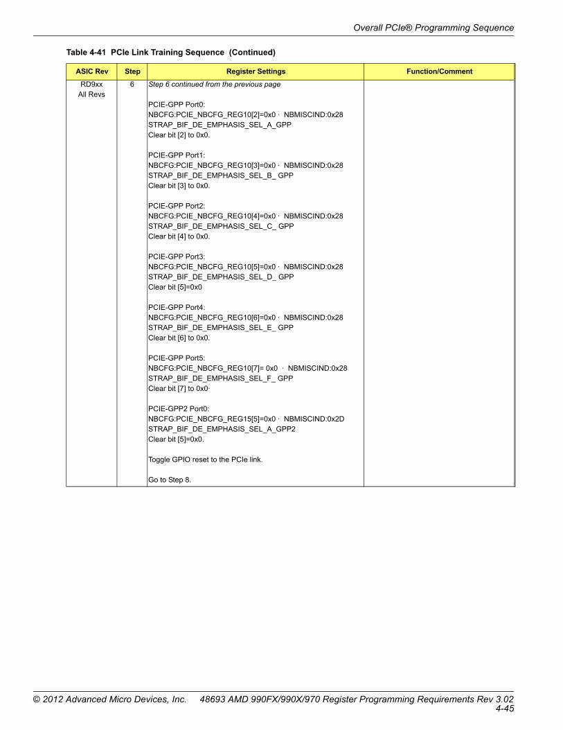
Overall PCIe® Programming Sequence
RD9xx All Revs
6 Step 6 continued from the previous page
PCIE-GPP Port0:NBCFG:PCIE_NBCFG_REG10[2]=0x0 · NBMISCIND:0x28STRAP_BIF_DE_EMPHASIS_SEL_A_GPPClear bit [2] to 0x0.
PCIE-GPP Port1:NBCFG:PCIE_NBCFG_REG10[3]=0x0 · NBMISCIND:0x28 STRAP_BIF_DE_EMPHASIS_SEL_B_ GPPClear bit [3] to 0x0.
PCIE-GPP Port2:NBCFG:PCIE_NBCFG_REG10[4]=0x0 · NBMISCIND:0x28 STRAP_BIF_DE_EMPHASIS_SEL_C_ GPPClear bit [4] to 0x0.
PCIE-GPP Port3:NBCFG:PCIE_NBCFG_REG10[5]=0x0 · NBMISCIND:0x28STRAP_BIF_DE_EMPHASIS_SEL_D_ GPPClear bit [5]=0x0
PCIE-GPP Port4:NBCFG:PCIE_NBCFG_REG10[6]=0x0 · NBMISCIND:0x28 STRAP_BIF_DE_EMPHASIS_SEL_E_ GPPClear bit [6] to 0x0.
PCIE-GPP Port5:NBCFG:PCIE_NBCFG_REG10[7]= 0x0 · NBMISCIND:0x28 STRAP_BIF_DE_EMPHASIS_SEL_F_ GPPClear bit [7] to 0x0·
PCIE-GPP2 Port0:NBCFG:PCIE_NBCFG_REG15[5]=0x0 · NBMISCIND:0x2D STRAP_BIF_DE_EMPHASIS_SEL_A_GPP2Clear bit [5]=0x0.
Toggle GPIO reset to the PCIe link.
Go to Step 8.
Table 4-41 PCIe Link Training Sequence (Continued)
ASIC Rev Step Register Settings Function/Comment
© 2012 Advanced Micro Devices, Inc. 48693 AMD 990FX/990X/970 Register Programming Requirements Rev 3.024-45

Overall PCIe® Programming Sequence
RD9xx All Revs
7 BIF_NBP:PCIE_LC_STATE0 · PCIEIND_P:0xA5 Read back the following values:LC_CURRENT_STATE = [5:0]LC_PREV_STATE1 = [13:8]LC_PREV_STATE2 = [21:16]LC_PREV_STATE3 = [29:24]
If the read back value of 0x062A or 0x092A is found in any of the fields above, set the following registers to the values specified below:BIF_NBP:LINK_CNTL2[3:0]=0x1 · pcieCopcieConfigDev*:0x88 TARGET_LINK_SPEEDSet bits [3:0] to 0x1.
BIF_NBP:PCIE_LC_SPEED_CNTL[0]=0x0 · PCIEIND_P:0xA4 LC_GEN2_EN_STRAPClear bit [0] to 0x0.
BIF_NBP:PCIE_LC_LINK_WIDTH_CNTL[13]=0x1 · PCIEIND_P:0xA2 LC_UPCONFIGURE_DISSet bit [13] to 0x1.
and for the link in training clear corresponding de-emphasis select bit:PCIE-GFX Port0:NBCFG:PCIE_NBCFG_REG10[0]=0x0 · NBMISCIND:0x28 STRAP_BIF_DE_EMPHASIS_SEL_A_GFXClear bit [0] to 0x0.
PCIE-GFX Port1:NBCFG:PCIE_NBCFG_REG10[1]=0x0 · NBMISCIND:0x28 STRAP_BIF_DE_EMPHASIS_SEL_B_GFXClear bit [1] to 0x0.
PCIE-GFX2 Port0:NBCFG:PCIE_NBCFG_REGF[30]=0x0 · NBMISCIND:0x27STRAP_BIF_DE_EMPHASIS_SEL_A_GFX2Clear bit [30] to 0x0.
PCIE-GFX2 Port1:NBCFG:PCIE_NBCFG_REGF[31]=0x0 · NBMISCIND:0x27STRAP_BIF_DE_EMPHASIS_SEL_B_GFX2Clear bit [31] to 0x0.
PCIE-GPP Port0:NBCFG:PCIE_NBCFG_REG10[2]=0x0 · NBMISCIND:0x28STRAP_BIF_DE_EMPHASIS_SEL_A_GPPClear bit [2] to 0x0.
to be continued on the next page
CMOS Option (RC Advertised Gen2 Part 2 - Disabled by Default)
Table 4-41 PCIe Link Training Sequence (Continued)
ASIC Rev Step Register Settings Function/Comment
48693 AMD 990FX/990X/970 Register Programming Requirements Rev 3.02 © 2012 Advanced Micro Devices, Inc.4-46

Overall PCIe® Programming Sequence
RD9xx All Revs
7 Step 7 continued from the previous page
PCIE-GPP Port1:NBCFG:PCIE_NBCFG_REG10[3]=0x0 · NBMISCIND:0x28 STRAP_BIF_DE_EMPHASIS_SEL_B_ GPPClear bit [3] to 0x0.
PCIE-GPP Port2:NBCFG:PCIE_NBCFG_REG10[4]=0x0 · NBMISCIND:0x28 STRAP_BIF_DE_EMPHASIS_SEL_C_ GPPClear bit [4] to 0x0.
PCIE-GPP Port3:NBCFG:PCIE_NBCFG_REG10[5]=0x0 · NBMISCIND:0x28STRAP_BIF_DE_EMPHASIS_SEL_D_ GPPClear bit [5] to 0x0.
PCIE-GPP Port4:NBCFG:PCIE_NBCFG_REG10[6]=0x0 · NBMISCIND:0x28 STRAP_BIF_DE_EMPHASIS_SEL_E_ GPPClear bit [6] to 0x0.
PCIE-GPP Port5:NBCFG:PCIE_NBCFG_REG10[7]= 0x0 · NBMISCIND:0x28 STRAP_BIF_DE_EMPHASIS_SEL_F_ GPPClear bit [7] to 0x0·
PCIE-GPP2 Port0:NBCFG:PCIE_NBCFG_REG15[5]=0x0 · NBMISCIND:0x2D STRAP_BIF_DE_EMPHASIS_SEL_A_GPP2Clear bit [5] to 0x0.
Toggle GPIO reset to the PCIe link.
Go to Step 8.
8 BIF_NBP:PCIE_LC_STATE0 · PCIEIND_P:0xA5 LC_CURRENT_STATE
Read back bits [5:0].
If LC_CURRENT_STATE = 0x07 -> Device is in compliance state (training sequence is done). Move to train the next device;
If LC_CURRENT_STATE = 0x10 -> go to Step 9
Otherwise, keep polling for up to 2 seconds, then perform CF9 reset. This should only be repeated for a maximum of 15 times.
If LC_CURRENT_STATE can not reach 0x10 or 0x07 -> go to Step 13.
Detects if link is in Compliance State or it is trained to L0 from reading back PCIE_LC_STATE0 [5:0] in Device*.
Table 4-41 PCIe Link Training Sequence (Continued)
ASIC Rev Step Register Settings Function/Comment
© 2012 Advanced Micro Devices, Inc. 48693 AMD 990FX/990X/970 Register Programming Requirements Rev 3.024-47

Overall PCIe® Programming Sequence
RD9xx All Revs
9 BIF_NBP:PCIE_VC0_RESOURCE_STATUS[1] · pcieConfigDev*:0x12aVC_NEGOTIATION_PENDING
Read bit [1].
Read back value of 0x0 means link negotiation is successful -> go to Step 11.
Read back value of 0x1 means the link needs to be re-trained -> go to step 10.
Detects if Data Link Negotiation is performed, by reading bit [1] of BIF_NBP:PCIE_VC0_RESOURCE_STATUS[1] · pcieConfigDev*:0x12a
10 For the following register, set bit [8] and make bits [2:0] to be equal to bits [6:4]:BIF_NBP:PCIE_LC_LINK_WIDTH_CNTL PCIEIND_P:0xA2 LC_RECONFIG_NOW, bit [8]LC_LINK_WIDTH, bit [2:0] <- LC_LINK_WIDTH_RD, bit [6:4]
Wait for 5ms after the bits above are set, and then go back to step 2 (stay in this loop indefinitely).
Retrains the link.
RD9xxAll Revs
11 NOTE: This step is required only for RD9xx client platforms.For AMD GFX cards only -> go to section Section 4.4.8.1 ”Workaround for Broadcom 5709C ASPM L1 Issue” on page 4-76 for RV370/RV380 Graphics Card Initialization .
RV370/RV380 Initialization Workaround.
RD9xxAll Revs
12 After the implementation of RV370/RV380 Initialization Workaround, and after reading back the Device ID for the non-AMD Device, as well as AMD devices for which this workaround is not applicable, perform the following:BIF_NB:PCIE_CI_CNTL[9]=0x0· PCIEIND:0x20 CI_RC_ORDERING_DIS
Clear bit [9] to 0x0.
Enable RC ordering logic.
RD9xx All Revs
13 1. Hide the bridge2. Set the hold training bit to 1 (find the corresponding bit from Step 1);3. Power down the port, than move to the train the next device.
When the link cannot be trained properly, these 3 steps should be performed.
Table 4-41 PCIe Link Training Sequence (Continued)
ASIC Rev Step Register Settings Function/Comment
48693 AMD 990FX/990X/970 Register Programming Requirements Rev 3.02 © 2012 Advanced Micro Devices, Inc.4-48

Overall PCIe® Programming Sequence
4.4.4 PCIe® Power Control
4.4.4.1 Dynamic Link Width Control (CMOS Option)
• Step 18: Dynamic Link Width Control (CMOS Option)
Dynamic Link Width Control is a power saving feature that allows fewer PCIe lanes to be active as compared to the number of lanes physically connected on the PCIe link. This feature is initiated by software and completely controlled by hardware.
The following CMOS options are available:
• PCIE-GFX Port 0 Link Width: x16, x8, x4, x2, x1
• PCIE-GFX Port 1 Link Width: x8, x4, x2, x1 [NOTE: This CMOS option should be available only in Dual Port configuration and greyed out in Single Port configuration]
• PCIE-GFX2 Port 0 Link Width: x16, x8, x4, x2, x1
• PCIE-GFX2 Port 1 Link Width: x8, x4,x2,x1 [NOTE: This CMOS option should be available only in Dual Port configuration and grey out in Single Port configuration]
• PCIE-SB Port 0 Link Width: x4, x2, x1
• PCIE-GPP Port 0 Link Width: x4, x2, x1
• PCIE-GPP Port 1 Link Width: x2, x1
• PCIE-GPP Port 2 Link Width: x2, x1
• PCIE-GPP Port 3 Link Width: x1
• PCIE-GPP Port 4 Link Width: x1
• PCIE-GPP Port 5 Link Width: x1
• PCIE-GPP2 Port 0 Link Width: x4, x2, x1 (Not applicable to RD980 and RX980)
If the Southbridge has low bandwidth requirements, for example, when SATA ports are not utilized, it is recommended to configure the northbridge-southbridge link in x1 in order to reduce power consumption.
There are two methods of dynamic link width control:
• Long Reconfiguration (The link goes down and retrains to a different width)
• Up/Down Reconfiguration (PCIe 2.0 Base Specification Compliant Link Width Reconfiguration)
4.4.4.1.1 Long Reconfiguration
Long reconfiguration is used with v1.1 or v1.0a PCIe specification compliant endpoint devices. This method of changing the number of active lanes causes the link to go down and is not recommended on an already active PCIe link without making sure that there is no traffic on the link during link width reconfiguration described in table below.
Table 4-42 Long Reconfiguration
ASIC Rev Step Register Settings Function/Comment
RD9xxAll Revs
1 BIF_NBP:PCIE_LC_LINK_WIDTH_CNTL[2:0] · PCIEIND_P:0xA2 LC_LINK_WIDTH
Set bits [2:0] to desired link width.
Sets the desired link width using the encoding scheme of the link width:000 = x16001 = x1010 = x2011 = x4100 = x8101 = x12 (not supported)110 = x16 based on CMOS option selected.
© 2012 Advanced Micro Devices, Inc. 48693 AMD 990FX/990X/970 Register Programming Requirements Rev 3.024-49

Overall PCIe® Programming Sequence
RD9xxAll Revs
2 Read back current link width by reading bits [6:4] of the following register:BIF_NBP:PCIE_LC_LINK_WIDTH_CNTL[6:4] · PCIEIND_P:0xA2LC_LINK_WIDTH_RD
Read back intended link width by reading bits [2:0] of the same register:BIF_NBP:PCIE_LC_LINK_WIDTH_CNTL[2:0] · PCIEIND_P:0xA2 LC_LINK_WIDTH
If the current link width is less than the intended link width based on the CMOS option selected, then grey out the link width selected in the CMOS option and skip this sequence.
If the current link width is equal 101, then the link must be retrained to x8, and then proceed with the sequence, and in step 4 set desired link width to 100.
If the current link width is equal to the intended link width, then skip this sequence.
If the current link width is greater than the intended link width, then proceed with the sequence.
This step prevents users from trying to train the link to greater link width than maximum value limited with number of physical lanes connected on PCIE link.
This step prevents users from trying to train the link in x12, and it downgrades to the first lower link width value supported, which is x8.
3 BIF_NB:PCIE_P_CNTL[0]=0x1 · PCIEIND:0x40 P_PWRDN_EN
Set bit [0] to 0x1.
In the proprietary register space of the AMD graphics card located behind the device that is initiating reconfiguration, set:
BIF:PCIE_P_CNTL[0]=0x0 · PCIEIND:0xB0 P_PWRDN_EN
Set bit [0] to 0x0.
Enables powering down transmitter and receiver pads along with PLL macros.
For AMD graphics devices only.
4 BIF_NBP:PCIE_LC_LINK_WIDTH_CNTL[7]=0x1 · PCIEIND_P:0xA2 LC_RECONFIG_ARC_MISSING_ESCAPE Set bit [7] to 0x1.
For Long Reconfiguration shorten the timeout from Recovery.Idle to Detect
5 BIF_NBP:PCIE_LC_LINK_WIDTH_CNTL[8]=0x1 · PCIEIND_P:0xA2 LC_RECONFIG_NOW
Set bit [8] to 0x1.
Starts reconfiguration.
6 BIF_NBP:LINK_STATUS[11] · pcieConfigDev*:0x6a LINK_TRAINING
Poll bit [11] until 0x0.
Ensures that link training is completed. Hardware clears this bit once link training is complete.
7 BIF_NBP:PCIE_LC_LINK_WIDTH_CNTL[8] · PCIEIND_P:0xA2 LC_RECONFIG_NOW
Poll bit [8] until 0x0
Ensures that reconfiguration is completed. Hardware clears this bit once reconfiguration is complete.
8 BIF_NBP:PCIE_VC0_RESOURCE_STATUS[1] · pcieConfigDev*:0x12aVC_NEGOTIATION_PENDING
Poll bit [1] until 0x0
Ensures that virtual channel negotiation is done.
Table 4-42 Long Reconfiguration (Continued)
ASIC Rev Step Register Settings Function/Comment
48693 AMD 990FX/990X/970 Register Programming Requirements Rev 3.02 © 2012 Advanced Micro Devices, Inc.4-50

Overall PCIe® Programming Sequence
4.4.4.1.2 Up/Down Reconfiguration
Up/Down Reconfiguration is feasible only with PCIe® 2.0 Base Specification compliant endpoint devices. To allow PCIe link to train to a shorter link width than that defined with the numbers of physical lanes connected in the link, follow the programming sequence specified below.
RD9xxAll Revs
9 Link width change is completed.
Power down unused lanes.
Unused lanes should be powered off. Follow steps for powering down unused lanes described in Section 4.4.2 ”PCIe® Cores Initialization” on page 4-17
10 BIF_NB:PCIE_P_CNTL[0]=0x0 · PCIEIND:0x40 P_PWRDN_EN
Clear bit [0] to 0x0.
On the AMD end points, behind the device initiating reconfiguration:BIF:PCIE_P_CNTL[0]=0x1 · PCIEIND:0xB0 P_PWRDN_EN
Set bit [0] to 0x1.
Disables powering down transmitter and receiver pads along with PLL macros.
For AMD graphics cards only in dual PCIE-GFX or PCIE- GFX2 configuration.
11 BIF_NBP:PCIE_LC_LINK_WIDTH_CNTL[7]=0x0 · PCIEIND_P:0xA2 LC_RECONFIG_ARC_MISSING_ESCAPE Clear bit [7] to 0x0.
Clears the register which shortens the timeout from Recovery.Idle to Detect for Long Reconfiguration.
Table 4-43 Up/Down Reconfiguration
ASIC Rev Step Register Settings Function/Comment
RD9xx
All Revs
1 Read back bit [9] of the following register:BIF_NBP:PCIE_LC_LINK_WIDTH_CNTL[9] · PCIEIND_P:0xA2 LC_RENEGOTIATION_SUPPORT
If the read back value of bit [9] is 0x0, then skip this sequence; otherwise go to step 2.
Checks if the endpoint device supports Up/Down Reconfiguration.
2 BIF_NBP:PCIE_LC_LINK_WIDTH_CNTL[12]=0x1 · PCIEIND_P:0xA2 LC_UPCONFIGURE_SUPPORT
Set bit [12] to 1.
Advertises support for Up/Down Reconfiguration.
3 BIF_NBP:PCIE_LC_LINK_WIDTH_CNTL[2:0] · PCIEIND_P:0xA2 LC_LINK_WIDTH
Set bits [2:0] to desired link width.
Sets the desired link width using the encoding scheme:000 = x16001 = x1010 = x2011 = x4100 = x8101 = x12 (not supported)110 = x16based on CMOS option selected.
Table 4-42 Long Reconfiguration (Continued)
ASIC Rev Step Register Settings Function/Comment
© 2012 Advanced Micro Devices, Inc. 48693 AMD 990FX/990X/970 Register Programming Requirements Rev 3.024-51

Overall PCIe® Programming Sequence
RD9xx
All Revs
4 Read back current link width by reading bits [6:4] of the following register:BIF_NBP:PCIE_LC_LINK_WIDTH_CNTL[6:4] · PCIEIND_P:0xA2LC_LINK_WIDTH_RD
Read back intended link width by reading bits [2:0] of the same register:BIF_NBP:PCIE_LC_LINK_WIDTH_CNTL[2:0] · PCIEIND_P:0xA2 LC_LINK_WIDTH
If the current link width is less than the intended link width based on the CMOS option selected, then grey out the link width selected in the CMOS option and skip this sequence.
If the current link width is equal to 3’b101, the link must be retrained to x8, and then proceed with the sequence, and in step 4 set desired link width to 3’b100.
If the current link width is equal to the intended link width, skip this sequence.
If the current link width is greater than intended link width, then proceed with the sequence.
This step prevents users from trying to train the link to greater link width than maximum value limited by the number of physical lanes connected on PCIE link.
This step prevents users from trying to train the link in x12, and it downgrades to the first lower link width value supported, which is x8.
5 For AMD end point only, in the proprietary register space of AMD graphics device:BIF_NBP:PCIE_LC_CNTL2[23]=0x1· PCIEIND_P:0xB1 LC_WAIT_FOR_LANES_IN_LW
Set bit [23] to 0x1.
Makes ConfigStep2-2b timeout 1us.
6 BIF_NBP:PCIE_LC_LINK_WIDTH_CNTL[10]=0x1 · PCIEIND_P:0xA2LC_RENEGOTIATE_EN
Set bit [10] to 0x1.
Enables Up/Down Reconfiguration
7 BIF_NBP:PCIE_LC_LINK_WIDTH_CNTL[8]=0x1 · PCIEIND_P:0xA2 LC_RECONFIG_NOW
Set bit [8] to 0x1.
Starts Up/Down Reconfiguration
Table 4-43 Up/Down Reconfiguration (Continued)
ASIC Rev Step Register Settings Function/Comment
48693 AMD 990FX/990X/970 Register Programming Requirements Rev 3.02 © 2012 Advanced Micro Devices, Inc.4-52

Overall PCIe® Programming Sequence
4.4.5 Static PCIe® Port Power Down Control
• Step 19: Static PCIe Port Power Down Control
• Step 19.1: Instructions for Non-Connected GFX/GFX2REFCLK
• Step 19.2: PCIE-GFX Port 0 (Device 2) Power Down Control – Single/Dual PCIE-GFX Link Configuration
Table 4-44 Instructions for Non-Connected GFX/GFX2REFCLK
ASIC Rev Step Register Settings Function/Comment
RD9xxAll Revs
1 NBCFG:PCIE_PDNB_CNTL[0] = 0x1 · NBMISCIND:0x7TXCLK_OFF_GFXSet bit [0] to 0x1.
This step must be performed for any design where GFX_REFCLK is not connected at the platform level.
2 NBCFG:PCIE_PDNB_CNTL[1] = 0x1 · NBMISCIND:0x7TXCLK_OFF_GFX2Set bit [1] to 0x1.
This step must be performed for any RD9xx design where GFX2_REFCLK is not connected at the platform level.
Table 4-45 PCIE-GFX Port 0 (Device 2) Power Down Control Programming Sequence
ASIC Rev Step Register Settings Function/Comment
RD9xxAll Revs
1 If link width is x8 in PCIE- GFX Single Configuration, and Lane Reversal is NOT enabled in CMOS:BIF_NB:PCIE_P_PAD_FORCE_DIS[15:0] = 0xF0F0 ·PCIEIND:0x65
NBCFG:PCIE_NBCFG_REGB [1] = 0x1 · NBMISCIND:0x23 B_PPLL_PDNB_FDIS[1]NBCFG:PCIE_NBCFG_REGB [3] = 0x1 · NBMISCIND:0x23 B_PPLL_BUF_PDNB_FDIS[1]
Turns off Tx/RX PADs for Ln8-15.Turns off PLL1.
2 If link width is x8 in PCIE- GFX Single Configuration, and Lane Reversal is enabled: BIF_NB:PCIE_P_PAD_FORCE_DIS[15:0]= 0x0F0F · PCIEIND:0x65 Turn off PLL0:NBCFG:PCIE_NBCFG_REGB [0]=0x1 · NBMISCIND:0x23 B_PPLL_PDNB_FDIS[0]NBCFG:PCIE_NBCFG_REGB [2]=0x1 · NBMISCIND:0x23 B_PPLL_BUF_PDNB_FDIS[0]
Turns off Tx/RX PADs for Ln0-7Turns off PLL0 for Lane Reversed PCIE-GFX Single Configuration.
3 If link width is x4 in PCIE- GFX Single Configuration, and Lane Reversal is NOT enabled in CMOS:BIF_NB:PCIE_P_PAD_FORCE_DIS[15:0]= 0xFCFC · PCIEIND:0x65
For PCIE-GFX Single configuration, turn off PLL1:NBCFG:PCIE_NBCFG_REGB [1]=0x1 · NBMISCIND:0x23 B_PPLL_PDNB_FDIS[1]NBCFG:PCIE_NBCFG_REGB [3]=0x1 · NBMISCIND:0x23 B_PPLL_BUF_PDNB_FDIS[1]
Turns off Tx/RX PADs for Ln5-15.Turns off PLL1 in PCIE-GFX Single Configuration.
4 If link width is x4 in PCIE-GFX Dual Configuration, and Lane Reversal is NOT enabled in CMOS:BIF_NB:PCIE_P_PAD_FORCE_DIS[3:0]= 0xC · PCIEIND:0x65 BIF_NB:PCIE_P_PAD_FORCE_DIS[11:8]= 0xC · PCIEIND:0x65
Turns off Tx/RX PADs for Ln4-7
5 If Llink width is x4 in PCIE- GFX Single Configuration, and Lane Reversal is enabled in CMOS:BIF_NB:PCIE_P_PAD_FORCE_DIS[15:0]= 0x3F3F · PCIEIND:0x65 Turn off PLL0:NBCFG:PCIE_NBCFG_REGB [0]=0x1 · NBMISCIND:0x23 B_PPLL_PDNB_FDIS[0]NBCFG:PCIE_NBCFG_REGB [2]=0x1 · NBMISCIND:0x23 B_PPLL_BUF_PDNB_FDIS[0]
Turns off Tx/RX PADs for Ln0-11.Turns off PLL0 for Lane Reversed PCIE-GFX Single Configuration.
© 2012 Advanced Micro Devices, Inc. 48693 AMD 990FX/990X/970 Register Programming Requirements Rev 3.024-53

Overall PCIe® Programming Sequence
• Step 19.3: PCIE-GFX Port 1 (Device3) Power Down Control – Dual PCIE-GFX Configuration
RD9xxAll Revs
6 If link width is x4 in PCIE- GFX Dual Configuration, and Lane Reversal is enabled in CMOS:BIF_NB:PCIE_P_PAD_FORCE_DIS[3:0]= 0x3 · PCIEIND:0x65BIF_NB:PCIE_P_PAD_FORCE_DIS[11:8]= 0x3 · PCIEIND:0x65
Turns off Tx/RX PADs for Ln0-3.
7 If link width is x2 in PCIE-GFX Single Configuration, and Lane Reversal is NOT enabled in CMOS:BIF_NB:PCIE_P_PAD_FORCE_DIS[15:0]= 0xFEFE · PCIEIND:0x65
For PCIE-GFX Single configuration, turn off PLL1:NBCFG:PCIE_NBCFG_REGB [1]=0x1 · NBMISCIND:0x23 B_PPLL_PDNB_FDIS[1]NBCFG:PCIE_NBCFG_REGB [3]=0x1 · NBMISCIND:0x23 B_PPLL_BUF_PDNB_FDIS[1]
Turns off Tx/RX PADs for Ln2-15.Turns off PLL1 in PCIE-GFX Single Configuration.
8 If link width is x2 in PCIE- GFX Dual Configuration, and Lane Reversal is NOT enabled in CMOS:BIF_NB:PCIE_P_PAD_FORCE_DIS[3:0]= 0xE · PCIEIND:0x65 BIF_NB:PCIE_P_PAD_FORCE_DIS[11:8]= 0xE · PCIEIND:0x65
Turns off Tx/RX PADs for Ln2-7
9 If link width is x2 in PCIE- GFX Single Configuration, and Lane Reversal is enabled in CMOS:BIF_NB:PCIE_P_PAD_FORCE_DIS[15:0]= 0x7F7F · PCIEIND:0x65 Turn off PLL0:NBCFG:PCIE_NBCFG_REGB [0]=0x1 · NBMISCIND:0x23 B_PPLL_PDNB_FDIS[0]NBCFG:PCIE_NBCFG_REGB [2]=0x1 · NBMISCIND:0x23 B_PPLL_BUF_PDNB_FDIS[0]
Turns off Tx/RX PADs for Ln0-13.Turns off PLL1 in PCIE-GFX Single Configuration.Turns off PLL0 for Lane Reversed PCIE-GFX Single Configuration.
10 If link width is x2 in PCIE- GFX Dual Configuration, and Lane Reversal is enabled in CMOS:BIF_NB:PCIE_P_PAD_FORCE_DIS[3:0]= 0x7 · PCIEIND:0x65BIF_NB:PCIE_P_PAD_FORCE_DIS[11:8]= 0x7 · PCIEIND:0x65
Turns off Tx/RX PADs for Ln0-5.
11 For PCIE- GFX Single Configuration, Port 0 can be completely powered down if no device is detected or link training cannot be completed:This step and should also be executed for RD980/RX980 always. This step should also be executed if GFX_REFCLK is not connected at the platform level.
NBCFG:PCIE_NBCFG_REGB [3:0]=0xF · NBMISCIND:0x23
Powers down PLLs for PCIE-GFX and switch to reference clock.
12 For PCIE-GFX Dual Configuration, Port 0 can be completely powered down if no device is detected or link training can not be completed:BIF_NB:PCIE_P_PAD_FORCE_DIS[15:0]= 0xFFFF · PCIEIND:0x65
Powers down Tx/Rx pads for PCIE-GFX
13 For PCIE-GFX Dual Configuration, Port 0 can be completely powered down if no device is detected or link training can not be completed:BIF_NB:PCIE_P_PAD_FORCE_DIS[3:0]= 0xF · PCIEIND:0x65BIF_NB:PCIE_P_PAD_FORCE_DIS[11:8]= 0xF · PCIEIND:0x65 NOTE: PLL0 cannot be shut down as PCIE-GFX core needs clocks from PLL0.
Powers Down Port 0 in PCIE-GFX Dual Configuration
Table 4-45 PCIE-GFX Port 0 (Device 2) Power Down Control Programming Sequence (Continued)
ASIC Rev Step Register Settings Function/Comment
48693 AMD 990FX/990X/970 Register Programming Requirements Rev 3.02 © 2012 Advanced Micro Devices, Inc.4-54

Overall PCIe® Programming Sequence
• Step 19.4: PCIE-GFX2 Port 0 (Device 11) Power Down Control – Single/Dual PCIE-GFX2 Configuration
Table 4-46 PCIE-GFX Port 1 (Device 3) Power Down Control Programming Sequence
ASIC Rev Step Register Settings Function/Comment
RD9xx All Revs
1 If link width is x4 in PCIE-GFX Dual Configuration, and Lane Reversal
is NOT enabled in CMOS:
BIF_NB:PCIE_P_PAD_FORCE_DIS[7:4]= 0xC · PCIEIND:0x65
BIF_NB:PCIE_P_PAD_FORCE_DIS[15:12]= 0xC · PCIEIND:0x65
Turns off Tx/RX PADs for Ln13-15
2 If link width is x4 in PCIE-GFX Dual Configuration, and Lane Reversal
is enabled in CMOS:
BIF_NB:PCIE_P_PAD_FORCE_DIS[7:4]= 0x3 · PCIEIND:0x65
BIF_NB:PCIE_P_PAD_FORCE_DIS[15:12]= 0x3 · PCIEIND:0x65
Turns off Tx/RX PADs for Ln8-11.
3 If link width is x2 in PCIE-GFX Dual Configuration, and Lane Reversal
is NOT enabled in CMOS:
BIF_NB:PCIE_P_PAD_FORCE_DIS[7:4]= 0xE · PCIEIND:0x65
BIF_NB:PCIE_P_PAD_FORCE_DIS[15:12]= 0xE · PCIEIND:0x65
Turns off Tx/RX PADs for Ln11-15.
4 If link width is x2 in PCIE-GFX Dual Configuration, and Lane Reversal
is enabled in CMOS:
BIF_NB:PCIE_P_PAD_FORCE_DIS[7:4]= 0x7 · PCIEIND:0x65
BIF_NB:PCIE_P_PAD_FORCE_DIS[15:12]= 0x7 · PCIEIND:0x65
Turns off Tx/RX PADs for Ln8-13.
5 Port 1 can be completely powered down if no device is detected or link
training can not be completed:
BIF_NB:PCIE_P_PAD_FORCE_DIS[7:4]= 0xF · PCIEIND:0x65
BIF_NB:PCIE_P_PAD_FORCE_DIS[15:12]= 0xF · PCIEIND:0x65
NBCFG:PCIE_NBCFG_REGB [1]=0x1 · NBMISCIND:0x23
NBCFG:PCIE_NBCFG_REGB [3]=0x1 · NBMISCIND:0x23
Powers Down PCIE-GFX Port B.
© 2012 Advanced Micro Devices, Inc. 48693 AMD 990FX/990X/970 Register Programming Requirements Rev 3.024-55

Overall PCIe® Programming Sequence
Table 4-47 PCIE-GFX2 Port 0 (Device 11) Power Down Control Programming Sequence
ASIC Rev Step Register Settings Function/Comment
RD9xx
All Revs
1 If link width is x8 in PCIE-GFX2 Single Configuration, and Lane Reversal
is NOT enabled in CMOS:
BIF_NB:PCIE_P_PAD_FORCE_DIS[15:0]= 0xF0F0 PCIEIND:0x65
NBCFG:PCIE_NBCFG_REGB [9]=0x1 · NBMISCIND:0x23
B_PPLL_PDNB_FDIS[1]
NBCFG:PCIE_NBCFG_REGB [11]=0x1 · NBMISCIND:0x23
B_PPLL_BUF_PDNB_FDIS[1]
NOTE: This step is not applicable to RD980/RX980.
Turns of Tx/RX PADs for Ln8-15.
Turns off PLL1.
2 If link width is x8 in PCIE-GFX2 Single Configuration, and Lane Reversal is
enabled:
BIF_NB:PCIE_P_PAD_FORCE_DIS[15:0]= 0x0F0F PCIEIND:0x65
NOTE: This step is not applicable to RD980/RX980.
Turn off PLL0:
NBCFG:PCIE_NBCFG_REGB [8]=0x1 · NBMISCIND:0x23
B_PPLL_PDNB_FDIS[0]
NBCFG:PCIE_NBCFG_REGB [10]=0x1 · NBMISCIND:0x23
B_PPLL_BUF_PDNB_FDIS[0]
NOTE: This step is not applicable to RD980/RX980.
Turns off Tx/RX PADs for Ln 0-7
Turnsoff PLL0 if PCIE-GFX2
Lane Reversal enabled.
Turns off PLL0 for Lane
Reversed PCIE-GFX2 Single
Configuration.
3 If link width is x4 in PCIE-GFX2 Single Configuration, and Lane Reversal is
NOT enabled in CMOS:
BIF_NB:PCIE_P_PAD_FORCE_DIS[15:0]= 0xFCFC · PCIEIND:0x65
For PCIE-2GPP2 Single configuration, turn off PLL1:
NBCFG:PCIE_NBCFG_REGB [9]=0x1 · NBMISCIND:0x23
B_PPLL_PDNB_FDIS[1]
NBCFG:PCIE_NBCFG_REGB [11]=0x1 · NBMISCIND:0x23
B_PPLL_BUF_PDNB_FDIS[1]
NOTE: This step is not applicable to RD980/RX980.
Turns off Tx/RX PADs for
Ln5-15.
Turns off PLL1 in PCIE-GFX2
Single Configuration.
4 If link width is x4 in PCIE-GFX2 Dual Configuration, and Lane Reversal is
NOT enabled in CMOS:
BIF_NB:PCIE_P_PAD_FORCE_DIS[3:0]= 0xC · PCIEIND:0x65
BIF_NB:PCIE_P_PAD_FORCE_DIS[11:8]= 0xC · PCIEIND:0x65
Turns off Tx/RX PADs for Ln4-7
5 If link width is x4 in PCIE-GFX2 Single Configuration, and Lane Reversal is
enabled in CMOS:
BIF_NB:PCIE_P_PAD_FORCE_DIS[15:0]= 0x3F3F · PCIEIND:0x65
NOTE: This step is not applicable to RD980/RX980.
Turn off PLL0:
NBCFG:PCIE_NBCFG_REGB [8]=0x1 · NBMISCIND:0x23
B_PPLL_PDNB_FDIS[0]
NBCFG:PCIE_NBCFG_REGB [10]=0x1 · NBMISCIND:0x23
B_PPLL_BUF_PDNB_FDIS[0]
NOTE: This step is not applicable to RD980/RX980.
Turns off Tx/RX PADs for Ln0-11.
Turns off PLL0 in PCIE-GFX2
Single Configuration.
Turns off PLL0 for Lane
Reversed PCIE-GFX2 Single
Configuration.
6 If link width is x4 in PCIE-GFX2 Dual Configuration and Lane Reversal is
enabled in CMOS:
BIF_NB:PCIE_P_PAD_FORCE_DIS[3:0]= 0x3 · PCIEIND:0x65
BIF_NB:PCIE_P_PAD_FORCE_DIS[11:8]= 0x3 · PCIEIND:0x65
Turns off Tx/RX PADs for Ln0-3.
48693 AMD 990FX/990X/970 Register Programming Requirements Rev 3.02 © 2012 Advanced Micro Devices, Inc.4-56

Overall PCIe® Programming Sequence
RD9xx
All Revs
7 If Link width is x2 in PCIE-GFX2 Single Configuration, and Lane Reversal
is NOT enabled in CMOS:
BIF_NB:PCIE_P_PAD_FORCE_DIS[15:0]= 0xFEFE · PCIEIND:0x65
For PCIE-2GPP2 Single configuration, turn off PLL1:
NBCFG:PCIE_NBCFG_REGB [9]=0x1 · NBMISCIND:0x23
B_PPLL_PDNB_FDIS[1]
NBCFG:PCIE_NBCFG_REGB [11]=0x1 · NBMISCIND:0x23
B_PPLL_BUF_PDNB_FDIS[1]
NOTE: This step is not applicable to RD980/RX980.
Turns off Tx/RX PADs for
Ln2-15.
Turns off PLL1 in PCIE-GFX2
Single Configuration.
8 If link width is x2 in PCIE-GFX2 Dual Configuration, and Lane Reversal is
NOT enabled in CMOS:
BIF_NB:PCIE_P_PAD_FORCE_DIS[3:0]= 0xE· PCIEIND:0x65
BIF_NB:PCIE_P_PAD_FORCE_DIS[11:8]= 0xE· PCIEIND:0x65
Turns off Tx/RX PADs for Ln2-7
9 If link width is x2 in PCIE-GFX2 Single Configuration, and Lane Reversal is enabled in CMOS:BIF_NB:PCIE_P_PAD_FORCE_DIS[15:0]= 0x7F7F · PCIEIND:0x65 NOTE: This step is not applicable to RD980/RX980.
Turn off PLL0:
NBCFG:PCIE_NBCFG_REGB [8]=0x1 · NBMISCIND:0x23
B_PPLL_PDNB_FDIS[0]
NBCFG:PCIE_NBCFG_REGB [10]=0x1 · NBMISCIND:0x23
B_PPLL_BUF_PDNB_FDIS[0]
NOTE: This step is not applicable to RD980/RX980.
Turns off Tx/RX PADs for
Ln0-13.
Turns off PLL0 in PCIE-GFX2
Single Configuration.
Turns off PLL0 for Lane
Reversed PCIE-GFX2 Single
Configuration.
10 If link width is x2 in PCIE-GFX2 Dual Configuration, and Lane Reversal is
enabled in CMOS:
BIF_NB:PCIE_P_PAD_FORCE_DIS[3:0]= 0x7 · PCIEIND:0x65
BIF_NB:PCIE_P_PAD_FORCE_DIS[11:8]= 0x7 · PCIEIND:0x65
Turns off Tx/RX PADs for Ln0-5.
11 For PCIE-GFX2 Single Configuration, Port 0 can be completely powered
down if no device is detected or link training cannot be completed:
This step should also be executed for RD980/RX980 always.
This step should also be executed for RD990 if GFX2_REFCLK is not
connected at the platform level.
NBCFG:PCIE_NBCFG_REGB [11:8]=0xF · NBMISCIND:0x23
Powers down PLL for
PCIE-GFX2 and switch to
reference clock
12 For PCIE-GFX2 Single Configuration, Port 0 can be completely powered
down if no device is detected or link training cannot be completed:
BIF_NB:PCIE_P_PAD_FORCE_DIS[15:0]= 0xFFFF · PCIEIND:0x65
Powers down Tx/Rx pads for
PCIE-GFX2
13 For PCIE-GFX2 Dual Configuration, Port 0 can be completely powered
down if no device is detected or link training cannot be completed:
BIF_NB:PCIE_P_PAD_FORCE_DIS[3:0]= 0xF · PCIEIND:0x65
BIF_NB:PCIE_P_PAD_FORCE_DIS[11:8]= 0xF · PCIEIND:0x65
NOTE: PLL0 can not be shut down as PCIE-GFX2 core needs clocks from
PLL0.
Powers down Port 0 in
PCIE-GFX2 Dual Configuration
Table 4-47 PCIE-GFX2 Port 0 (Device 11) Power Down Control Programming Sequence (Continued)
ASIC Rev Step Register Settings Function/Comment
© 2012 Advanced Micro Devices, Inc. 48693 AMD 990FX/990X/970 Register Programming Requirements Rev 3.024-57

Overall PCIe® Programming Sequence
• Step 19.5: PCIE-GFX2 Port 1 (Device 12) Power Down Control –Dual PCIE-GFX2 Configuration
• Step 19.6: PCIE-GPP Port 0 Power Down Control
If one or more PCIE-GPP Port 0 lanes are not used in the system, SBIOS can power down those lanes to save power. Refer to table below.
Table 4-48 PCIE-GFX2 Port 1 (Device12) Power Down Control Programming Sequence
ASIC Rev Step Register Settings Function/Comment
RD9xx
All Revs
1 If link width is x4 in PCIE-GFX2 Dual Configuration, and Lane Reversal
is NOT enabled in CMOS:
BIF_NB:PCIE_P_PAD_FORCE_DIS[7:4]=0xC · CIEIND:0x65
BIF_NB:PCIE_P_PAD_FORCE_DIS[15:12]= 0xC · PCIEIND:0x65
Turns off Tx/RX PADs for Ln13-15
2 If link width is x4 in PCIE-GFX2 Dual Configuration, and Lane Reversal
is enabled in CMOS:
BIF_NB:PCIE_P_PAD_FORCE_DIS[7:4]= 0x3 · PCIEIND:0x65
BIF_NB:PCIE_P_PAD_FORCE_DIS[15:12]= 0x3 · PCIEIND:0x65
Turns off Tx/RX PADs for Ln8-11.
3 If link width is x2 in PCIE-GFX2 Dual Configuration, and Lane Reversal
is NOT enabled in CMOS:
BIF_NB:PCIE_P_PAD_FORCE_DIS[7:4]= 0xE · PCIEIND:0x65
BIF_NB:PCIE_P_PAD_FORCE_DIS[15:12]= 0xE · PCIEIND:0x65
Turns off Tx/RX PADs for Ln11-15.
4 If link width is x2 in PCIE-GFX2 Dual Configuration, and Lane Reversal
is enabled in CMOS:
BIF_NB:PCIE_P_PAD_FORCE_DIS[7:4]= 0x7 · PCIEIND:0x65
BIF_NB:PCIE_P_PAD_FORCE_DIS[15:12]= 0x7 · PCIEIND:0x65
Turns off Tx/RX PADs for Ln8-13.
5 Port 1 can be completely powered down if no device is detected or link
training cannot be completed:
BIF_NB:PCIE_P_PAD_FORCE_DIS[7:4]= 0xF · PCIEIND:0x65
BIF_NB:PCIE_P_PAD_FORCE_DIS[15:12]= 0xF · PCIEIND:0x65
NBCFG:PCIE_NBCFG_REGB [9]=0x1 · NBMISCIND:0x23
NBCFG:PCIE_NBCFG_REGB [11]=0x1 · NBMISCIND:0x23
Powers Down PCIE-GFX2 Port 1.
Table 4-49 Power Down Unused Lanes for PCIE-GPP Port 0
PCIE-GPP Configuration BIF_NB:PCIE_P_PAD_FORCE_DIS[15:0] · PCIEIND:0x65
1:1:1:1:1:1 Turns off Tx/RX PADs for Ln0: BIF_NB:PCIE_P_PAD_FORCE_DIS[0]=0x1 · PCIEIND:0x65BIF_NB:PCIE_P_PAD_FORCE_DIS[8]=0x1 · PCIEIND:0x65
4:2:0:0:0:0 Turns off Tx/RX PADs for Ln0:BIF_NB:PCIE_P_PAD_FORCE_DIS[0]=0xF · PCIEIND:0x65BIF_NB:PCIE_P_PAD_FORCE_DIS[8]=0xF · PCIEIND:0x65
Turns off Tx/RX PADs for Ln1:BIF_NB:PCIE_P_PAD_FORCE_DIS[1]=0xF · PCIEIND:0x65BIF_NB:PCIE_P_PAD_FORCE_DIS[9]=0xF · PCIEIND:0x65
Turns off Tx/RX PADs for Ln2:BIF_NB:PCIE_P_PAD_FORCE_DIS[2]=0xF · PCIEIND:0x65BIF_NB:PCIE_P_PAD_FORCE_DIS[10]=0xF · PCIEIND:0x65
Turns off Tx/RX PADs for Ln3:BIF_NB:PCIE_P_PAD_FORCE_DIS[3]=0xF · PCIEIND:0x65BIF_NB:PCIE_P_PAD_FORCE_DIS[11]=0xF · PCIEIND:0x65
48693 AMD 990FX/990X/970 Register Programming Requirements Rev 3.02 © 2012 Advanced Micro Devices, Inc.4-58

Overall PCIe® Programming Sequence
• Step 19.7: PCIE-GPP Port 1 Power Down Control
If one or more PCIE-GPP Port 1 lanes are not used in the system, SBIOS can power down those lanes to save power. Refer to table below.
4:1:1:0:0:0 Turns off Tx/RX PADs for Ln0:BIF_NB:PCIE_P_PAD_FORCE_DIS[0]=0xf · PCIEIND:0x65BIF_NB:PCIE_P_PAD_FORCE_DIS[8]=0xf · PCIEIND:0x65
Turns off Tx/RX PADs for Ln1:BIF_NB:PCIE_P_PAD_FORCE_DIS[1]=0xF · PCIEIND:0x65BIF_NB:PCIE_P_PAD_FORCE_DIS[9]=0xF · PCIEIND:0x65
Turns off Tx/RX PADs for Ln2:BIF_NB:PCIE_P_PAD_FORCE_DIS[2]=0xF · PCIEIND:0x65BIF_NB:PCIE_P_PAD_FORCE_DIS[10]=0xF · PCIEIND:0x65
Turns off Tx/RX PADs for Ln3:BIF_NB:PCIE_P_PAD_FORCE_DIS[3]=0xF · PCIEIND:0x65BIF_NB:PCIE_P_PAD_FORCE_DIS[11]=0xF · PCIEIND:0x65
2:2:2:0:0:0 Turns off Tx/RX PADs for Ln0:BIF_NB:PCIE_P_PAD_FORCE_DIS[0]=0x3 · PCIEIND:0x65BIF_NB:PCIE_P_PAD_FORCE_DIS[8]=0x3 · PCIEIND:0x65
Turns off Tx/RX PADs for Ln1:BIF_NB:PCIE_P_PAD_FORCE_DIS[1]=0x3 · PCIEIND:0x65BIF_NB:PCIE_P_PAD_FORCE_DIS[9]=0x3 · PCIEIND:0x65
2:2:1:1:0:0 Turns off Tx/RX PADs for Ln0:BIF_NB:PCIE_P_PAD_FORCE_DIS[0]=0x3 · PCIEIND:0x65BIF_NB:PCIE_P_PAD_FORCE_DIS[8]=0x3 · PCIEIND:0x65
Turns off Tx/RX PADs for Ln1:BIF_NB:PCIE_P_PAD_FORCE_DIS[1]=0x3 · PCIEIND:0x65BIF_NB:PCIE_P_PAD_FORCE_DIS[9]=0x3 · PCIEIND:0x65
2:1:1:1:1:0 Turns off Tx/RX PADs for Ln0:BIF_NB:PCIE_P_PAD_FORCE_DIS[0]=0x3 · PCIEIND:0x65BIF_NB:PCIE_P_PAD_FORCE_DIS[8]=0x3 · PCIEIND:0x65
Turns off Tx/RX PADs for Ln1:BIF_NB:PCIE_P_PAD_FORCE_DIS[1]=0x3 · PCIEIND:0x65BIF_NB:PCIE_P_PAD_FORCE_DIS[9]=0x3 · PCIEIND:0x65
Table 4-50 Power Down Unused Lanes for PCIE-GPP Port 1
PCIE-GPP Configuration BIF_NB:PCIE_P_PAD_FORCE_DIS[15:0] · PCIEIND:0x65
1:1:1:1:1:1 Turns off Tx/RX PADs for Ln1:BIF_NB:PCIE_P_PAD_FORCE_DIS[1]=0x1 · PCIEIND:0x65BIF_NB:PCIE_P_PAD_FORCE_DIS[9]=0x1 · PCIEIND:0x65
4:2:0:0:0:0 Turns off Tx/RX PADs for Ln4:BIF_NB:PCIE_P_PAD_FORCE_DIS[4]=0x3 · PCIEIND:0x65BIF_NB:PCIE_P_PAD_FORCE_DIS[12]=0x3 · PCIEIND:0x65
Turns off Tx/RX PADs for Ln5:BIF_NB:PCIE_P_PAD_FORCE_DIS[5]=0x3 · PCIEIND:0x65BIF_NB:PCIE_P_PAD_FORCE_DIS[13]=0x3 · PCIEIND:0x65
4:1:1:0:0:0 Turns off Tx/RX PADs for Ln4:BIF_NB:PCIE_P_PAD_FORCE_DIS[4]=0x1 · PCIEIND:0x65BIF_NB:PCIE_P_PAD_FORCE_DIS[12]=0x1 · PCIEIND:0x65
Table 4-49 Power Down Unused Lanes for PCIE-GPP Port 0 (Continued)
PCIE-GPP Configuration BIF_NB:PCIE_P_PAD_FORCE_DIS[15:0] · PCIEIND:0x65
© 2012 Advanced Micro Devices, Inc. 48693 AMD 990FX/990X/970 Register Programming Requirements Rev 3.024-59

Overall PCIe® Programming Sequence
• Step 19.8: PCIE-GPP Port 2 Power Down Control
If one or more PCIE-GPP Port 2 lanes are not used in the system, SBIOS can power down those lanes to save power. Refer to table below.
2:2:2:0:0:0 Turns off Tx/RX PADs for Ln2:BIF_NB:PCIE_P_PAD_FORCE_DIS[2]=0x3 · PCIEIND:0x65BIF_NB:PCIE_P_PAD_FORCE_DIS[10]=0x3 · PCIEIND:0x65
Turns off Tx/RX PADs for Ln3:BIF_NB:PCIE_P_PAD_FORCE_DIS[3]=0x3 · PCIEIND:0x65BIF_NB:PCIE_P_PAD_FORCE_DIS[11]=0x3 · PCIEIND:0x65
2:2:1:1:0:0 Turns off Tx/RX PADs for Ln2:BIF_NB:PCIE_P_PAD_FORCE_DIS[2]=0x3 · PCIEIND:0x65BIF_NB:PCIE_P_PAD_FORCE_DIS[10]=0x3 · PCIEIND:0x65
Turns off Tx/RX PADs for Ln2-3:BIF_NB:PCIE_P_PAD_FORCE_DIS[3]=0x3 · PCIEIND:0x65BIF_NB:PCIE_P_PAD_FORCE_DIS[11]=0x3 · PCIEIND:0x65
2:1:1:1:1:0 Turns off Tx/RX PADs for Ln2:BIF_NB:PCIE_P_PAD_FORCE_DIS[2]=0x1 · PCIEIND:0x65BIF_NB:PCIE_P_PAD_FORCE_DIS[10]=0x1 · PCIEIND:0x65
Table 4-51 Powering Down unused lanes for PCIE-GPP Port 2
PCIE-GPP Configuration BIF_NB:PCIE_P_PAD_FORCE_DIS[15:0] · PCIEIND:0x65
1:1:1:1:1:1 Turns off Tx/RX PADs for Ln2:BIF_NB:PCIE_P_PAD_FORCE_DIS[2]=0x1 · PCIEIND:0x65BIF_NB:PCIE_P_PAD_FORCE_DIS[10]=0x1 · PCIEIND:0x65
4:2:0:0:0:0 N/A
4:1:1:0:0:0 Turns off Tx/RX PADs for Ln5:BIF_NB:PCIE_P_PAD_FORCE_DIS[5]=0x1 · PCIEIND:0x65BIF_NB:PCIE_P_PAD_FORCE_DIS[13]=0x1 · PCIEIND:0x65
2:2:2:0:0:0 Turns off Tx/RX PADs for Ln4:BIF_NB:PCIE_P_PAD_FORCE_DIS[4]=0x3 · PCIEIND:0x65BIF_NB:PCIE_P_PAD_FORCE_DIS[12]=0x3 · PCIEIND:0x65
Turns off Tx/RX PADs for Ln5:BIF_NB:PCIE_P_PAD_FORCE_DIS[5]=0x3 · PCIEIND:0x65BIF_NB:PCIE_P_PAD_FORCE_DIS[13]=0x3 · PCIEIND:0x65
2:2:1:1:0:0 Turns off Tx/RX PADs for Ln4:BIF_NB:PCIE_P_PAD_FORCE_DIS[4]=0x1 · PCIEIND:0x65BIF_NB:PCIE_P_PAD_FORCE_DIS[12]=0x1 · PCIEIND:0x65
2:1:1:1:1:0 Turns off Tx/RX PADs for Ln3:BIF_NB:PCIE_P_PAD_FORCE_DIS[3]=0x1 · PCIEIND:0x65BIF_NB:PCIE_P_PAD_FORCE_DIS[11]=0x1 · PCIEIND:0x65
Table 4-50 Power Down Unused Lanes for PCIE-GPP Port 1 (Continued)
PCIE-GPP Configuration BIF_NB:PCIE_P_PAD_FORCE_DIS[15:0] · PCIEIND:0x65
48693 AMD 990FX/990X/970 Register Programming Requirements Rev 3.02 © 2012 Advanced Micro Devices, Inc.4-60

Overall PCIe® Programming Sequence
• Step 19.9: PCIE-GPP Port 3 Power Down Control
If one or more PCIE-GPP Port 3 lanes are not used in the system, SBIOS can power down those lanes to save power. Refer to the table below.
• Step 19.10: PCIE-GPP Port 4 Power Down Control
If one or more PCIE-GPP Port 4 lanes are not used in the system, SBIOS can power down those lanes to save power. Refer to the table below.
• Step 19.11: PCIE-GPP Port 5 Power Down Control
If one or more PCIE-GPP Port 5 lanes are not used in the system, SBIOS can power down those lanes to save power. Refer to the table below.
Table 4-52 Powering Down Unused Lanes for PCIE-GPP Port 3
PCIE-GPP Configuration BIF_NB:PCIE_P_PAD_FORCE_DIS[15:0] · PCIEIND:0x65
1:1:1:1:1:1 Turns off Tx/RX PADs for Ln3:BIF_NB:PCIE_P_PAD_FORCE_DIS[3]=0x1 · PCIEIND:0x65BIF_NB:PCIE_P_PAD_FORCE_DIS[11]=0x1 · PCIEIND:0x65
4:2:0:0:0:0 N/A
4:1:1:0:0:0 N/A
2:2:2:0:0:0 N/A
2:2:1:1:0:0 Turns off Tx/RX PADs for Ln5:BIF_NB:PCIE_P_PAD_FORCE_DIS[5]=0x1 · PCIEIND:0x65BIF_NB:PCIE_P_PAD_FORCE_DIS[13]=0x1 · PCIEIND:0x65
2:1:1:1:1:0 Turns off Tx/RX PADs for Ln4:BIF_NB:PCIE_P_PAD_FORCE_DIS[4]=0x1 · PCIEIND:0x65BIF_NB:PCIE_P_PAD_FORCE_DIS[12]=0x1 · PCIEIND:0x65
Table 4-53 Power Down Unused Lanes for PCIE-GPP Port 4
PCIE-GPP Configuration BIF_NB:PCIE_P_PAD_FORCE_DIS[15:0] · PCIEIND:0x65
1:1:1:1:1:1 Turns off Tx/RX PADs for Ln4:BIF_NB:PCIE_P_PAD_FORCE_DIS[4]=0x1 · PCIEIND:0x65BIF_NB:PCIE_P_PAD_FORCE_DIS[12]=0x1 · PCIEIND:0x65
4:2:0:0:0:0 N/A
4:1:1:0:0:0 N/A
2:2:2:0:0:0 N/A
2:2:1:1:0:0 N/A
2:1:1:1:1:0 Turns off Tx/RX PADs for Ln5:BIF_NB:PCIE_P_PAD_FORCE_DIS[5]=0x1· PCIEIND:0x65BIF_NB:PCIE_P_PAD_FORCE_DIS[13]=0x1· PCIEIND:0x65
Table 4-54 Power Down Unused Lanes for PCIE-GPP Port 5
PCIE-GPP Configuration BIF_NB:PCIE_P_PAD_FORCE_DIS[15:0] · PCIEIND:0x65
1:1:1:1:1:1 Turns off Tx/RX PADs for Ln5:BIF_NB:PCIE_P_PAD_FORCE_DIS[5]=0x1 · PCIEIND:0x65BIF_NB:PCIE_P_PAD_FORCE_DIS[13]=0x1 · PCIEIND:0x65
4:2:0:0:0:0 N/A
4:1:1:0:0:0 N/A
2:2:2:0:0:0 N/A
2:2:1:1:0:0 N/A
2:1:1:1:1:0 N/A
© 2012 Advanced Micro Devices, Inc. 48693 AMD 990FX/990X/970 Register Programming Requirements Rev 3.024-61

Overall PCIe® Programming Sequence
• Step 19.12: Completing PCIE-GPP Power Down Control
Power down PLL and turn off Electrical Idle detectors when no GPP ports are used and no hot-plug device is supported. Refer to the table below.
• Step 19.13: PCIE-SB Power Down Control
• Step 19.14: PCIE-GPP2 Power Down Control
Table 4-55 PCIE-GPP Power Down Control
ASIC Rev Step Register Settings Function/Comment
RD9xx
All Revs
1 NBCFG:PCIE_NBCFG_REGB [18]=0x1 · NBMISCIND:0x23 B_PPLL_PDNB_FDIS[0] for GPPNBCFG:PCIE_NBCFG_REGB [16]=0x1 · NBMISCIND:0x23 B_PPLL_BUF_PDNB_FDIS[0] for GPP
Powers down PCIE-GPP PLL when no GPP ports are used and no hot-plug device is supported.
2 NBCFG:PCIE_NBCFG_REG7[2]=0x0 · NBMISCIND:0x37 B_PG2RX_IDLEDET_EN_GPPClear bit [2] to 0x0.
Turns off Electrical Idle Detectors.
Table 4-56 PCIE-SB Power Down Control
ASIC Rev Step Register Settings Function/Comment
RD9xxAll Revs
1 Read back bit[6:4] of:
BIF_NBP:PCIE_LC_LINK_WIDTH_CNTL[6:4] PCIEIND_P:0xA2
in Dev8 to determine the current link width.
If width is x4 skip this sequence
If width is x2 go to Step 32.12.2
If width is x1 go to Step 32.12.3
Encoding of LC_LINK_WIDTH_RD:
000 = x16
001 = x1
010 = x2
011 = x4
100 = x8
101 = x12 (not supported)
110 = x16
2 PCIE_P_PAD_FORCE_DIS[15:0]=0x0C0C · PCIEIND:0x65
Set bits[15:0] to 0x0C0C
Powers down SB Lanes 3&2
3 PCIE_P_PAD_FORCE_DIS[15:0]=0x0E0E · PCIEIND:0x65
Set bits[15:0] to 0x0E0E
Powers down SB Lanes 3-1
Table 4-57 PCIE-GPP2 Power Down Control
ASIC Rev Step Register Settings Function/Comment
RD9xx
All Revs
1 NBCFG:PCIE_NBCFG_REG16[6]=0x1 · NBMISCIND:0x2E B_PPLL_PDNB_FDIS[0] for PCIE-GPP2NBCFG:PCIE_NBCFG_REGB [8]=0x1 · NBMISCIND:0x23 B_PPLL_BUF_PDNB_FDIS[0] for PCIE-GPP2
Powers down PCIE-GPP2 PLL when no
device is plugged in and no hot-plug device
is supported, or, for RD980/RX980, where
GPP2 is not supported.
2 PCIE_P_PAD_FORCE_DIS[15:0]=0x0C0C · PCIEIND:0x65
Set bits[15:0] to 0x0C0C
Powers down PCI-GPP2 Lanes 3&2
3 PCIE_P_PAD_FORCE_DIS[15:0]=0x0E0E · PCIEIND:0x65
Set bits[15:0] to 0x0E0E
Powers down PCIE-GPP2 Lanes 3-1
4 PCIE_P_PAD_FORCE_DIS[15:0]=0x0E0E · PCIEIND:0x65
Set bits[15:0] to 0x0F0F
Powers down GPP2 Lanes 3-0
5 NBCFG:PCIE_NBCFG_REG7[7]=0x0 · NBMISCIND:0x37 B_PG2RX_IDLEDET_EN_GPP2Clear bit [7] to 0x0.
Turns off Electrical Idle Detectors when no
GPP2 lanes are used.
48693 AMD 990FX/990X/970 Register Programming Requirements Rev 3.02 © 2012 Advanced Micro Devices, Inc.4-62

Overall PCIe® Programming Sequence
4.4.6 PCIe® Enumeration and Special Features Programming Sequence
• Step 20: PCIe Enumeration and Special Features Programming Sequence
SBIOS scans all of the PCI buses looking for P2P bridges. When a P2P bridge is located, it is assigned bus numbers. All buses behind the bridge must reside between the secondary and subordinate bus numbers.
• Step 20.1: Program Common Clock Configuration
Follow the programming sequence described in the table below in order to determine common clocking configuration of components on opposite sides of each PCIe link crossing a connector and then report common clock configuration in LINK CONTROL register where applicable.
For all endpoint devices or switches integrated on the system board, SBIOS is responsible for correct programming of the Common Clock Configuration field of Link Control registers. SBIOS may reference the platform design guide specification in order to confirm common clock configuration.
• Step 20.2: Slot Power Limit
PCIe subsystem has in place software controllable mechanism to help the system control power budgeting for PCIe devices. This mechanism limits the maximum power per PCIe slot that PCIe adapter associated with that slot consumes.
System BIOS is responsible for the correct programming of Slot Power Limit Value and Slot Power Limit Scale fields of the Slot Capability registers of the downstream ports connected to the slot. After the value has been written into the register within the downstream port of root complex or switch connected to the slot, it is conveyed to the adapter using Set Slot Power Limit Message. It is then the responsibility of the device driver software associated with the adapter to configure the hardware on the adapter to guarantee that the adapter will not exceed the imposed limits.
For all endpoint devices or switches integrated on the system board, it is recommended that system BIOS reference platform design guide specification for power budget allocated to the device itself and reflects it in Slot Power Limit Message.
Table 4-58 Program Common Clock Configuration
ASIC Rev Step Register Settings Function/Comment
RD9xxAll Revs
1 Follow the capability list in the device's register space to find the PCIE capability (PCIe Capability ID = 0x12), then read bit [12] of LINK_STATUS register.PCIE_LINK_STAUS[12]=0x1 · (Offset =0x12 from PCIe Capability ID = 0x10).SLOT_CLOCK_CFG
For each endpoint device under the root port and all intervening device ports on that hierarchy on the adapter, determine whether the component on the adapter uses the clock supplied on the slot or one generated locally on the adapter.
2 BIF_NBP:PCIE_LINK_CNTL[6]=0x1· pcieConfigDev*:0x68COMMON_CLOCK_CFG
Set bit [6] to 0x1.
Follow the capability list in the device's register space to find the PCIe capability (PCIe Capability ID = 0x10), then set bit[6] of LINK_CNTL register to 0x1.PCIE_LINK_CNTL[6]=0x1· (Offset =0x10 from PCIe Capability ID = 0x10).
In the configuration space of root port and
each endpoint device under the root port and
all intervening device ports on that hierarchy
for which it was found in Step1 that
SLOT_CLOCK_CFG= 0x1 on both sides of
each PCIe link, indicate common reference
clock configuration.
3 BIF_NBP:PCIE_LINK_CNTL[5]=0x1· pcieConfigDev*:0x68RETRAIN_LINK
Set bit [5] to 0x1.
Re-train the link.
4 Read bit [11] of:
BIF_NBP:PCIE_LINK_STATUS[11] · pcieConfigDev*:0x6ALINK_TRAININGIf bit [11] = 0x0, exit the loop, if not, wait 1ms and read it again.If loop count = 100, exit the loop with the error flag set. This will cause the bridge to be hidden.
Check whether the link has completed
training.
© 2012 Advanced Micro Devices, Inc. 48693 AMD 990FX/990X/970 Register Programming Requirements Rev 3.024-63

Overall PCIe® Programming Sequence
The programming sequence outlined in the table below should be followed to program the Slot Power Limit Value and Slot Power Limit Scale fields of the Slot Capability registers of the RD9xx downstream ports connected to each PCIE slot.
• Step 21: Disable Immediate Timeout on Link Down
• Step 22: Register Locking
• Step 23: TXCLK, LCLK Gating for any PCIe core with no PCIe links being established on initial boot up
Table 4-59 Slot Power Limit Programming Sequence
ASIC Rev Step Register Settings Function/Comment
RD9xxAll Revs
1 BIF_NBP:SLOT_CAP[14:7] = 0x4B · pcieConfigDev*:0x6c
SLOT_PWR_LIMIT_VALUE
Set bits [14:7] to 0x4B.
BIF_NBP:SLOT_CAP[16:15]=0x0 · pcieConfigDev*:0x6c
SLOT_PWR_LIMIT_SCALE
Clear bits [16:15] to 0x0.
Slot Power Limit Value represents the maximum
power that the endpoint can draw from the PCIe
slot based on the maximum number of physical
lanes that the connector is designed for, the
form-factor of the card, etc. Root complex
convey this information to the endpoint through
Slot Power Limit Message based on the
programmed Slot Power Limit Value.
Default Slot Power Limit Value to 75W.
Implement x1 Multiplier.
Slot Power Limit Scale specifies the scale used
for the Slot Power Limit Value, and the available
range values are:
0x0 = 1.0 x Slot Power Limit Value,
0x1 = 0.1 x Slot Power Limit Value,
0x2 = 0.01 x Slot Power Limit Value,
0x3 = 0.001 x Slot Power Limit Value.
[NOTE:
A write to this register will cause the Port to
send the Set_Slot_Power_Limit_Message, so
both fields should be set with one register write.]
Table 4-61 Disabling Immediate Timeout on Link Down
ASIC Rev Step Register Settings Function/Comment
RD9xxAll Revs
1 BIF_NBP:PCIE_RX_CNTL[19] = 0x0 PCIEIND_P:0x70
RX_RCB_CPL_TIMEOUT_MODE
Clear bit [19] to 0x0.
Disables immediate RCB timeout on link down
Table 4-62 Register Locking Programming Sequence
ASIC Rev Step Register Settings Function/Comment
RD9xxAll Revs
1 BIF_NB:PCIE_CNTL[0]=0x1 · PCIEIND:0x10
HWINIT_WR_LOCK
Set bit [0] to 0x1.
Makes the HWINIT registers read-only for a PCIe
core
2 NBCFG:NB_CNTL[1]=0x1 · NBMISCIND:0x0
HIDE_NB_AGP_CAP
Set bit [0] to 0x1.
Hides AGP Capabilities
48693 AMD 990FX/990X/970 Register Programming Requirements Rev 3.02 © 2012 Advanced Micro Devices, Inc.4-64

Overall PCIe® Programming Sequence
To further reduce static power consumption, we can completely turn off TXCLK and LCLK branches going to unused PCIe cores. Each PCIe core (PCIE-GFX, PCIE-GFX2, PCIE-GPP, PCIE-GPP2) has a permanent (always-running) and dynamic (clock-gated) TXCLK and LCLK branch. When a core is not being used, both the permanent and dynamic branch to that core can be completely turned off to reduce power consumption.
The following describes the criteria and procedure for turning off PCIE TXCLK and LCLK branches. Note that the permanent LCLK branch for the PCIE-GFX core is also used by IOMMU andPCIE-GFX2 and PCIE-GPP2 cores, thus it can only be turned off if IOMMU is disabled and PCIE-GFX, PCIE-GFX2 and PCIE-GPP2 are not being used.
Note: On S3 resume, all associated registers must be restored at the end of the PCIe initialization sequence, because after these registers are restored (turning off the clocks), any register access to PCIe registers will no longer take effect.
© 2012 Advanced Micro Devices, Inc. 48693 AMD 990FX/990X/970 Register Programming Requirements Rev 3.024-65

Overall PCIe® Programming Sequence
Table 4-63 Turning off TXCLK and LCLK
ASIC Rev Step Register Settings Function/CommentRD9xx
All Revs1
NBCFG:PCIE_PDNB_CNTL[0]=0x1 · NBMISCIND:0x7 TXCLK_OFF_GFX
Set bit [0] to 0x1.
CLKCFG:CLK_TOP_SPARE_A[28]=0x1 · clkconfig:0xE0
Set bit [28] to 0x1.
NBCFG:PCIE_NBCFG_REGF[23]=0x1 · NBMISCIND:0x27 Force_off_LCLK_PCIE_GPP1
Set bit [23] to 0x1.
IOMMU_L2: L2_DEBUG_2[0]=0x1 · nbconfigfunc2:0x46
Set bit [0] to 0x1.
NOTE: This step must be performed for any design where GFX_REFCLK is not connected at the platform level.
Turn off TXCLK branches for PCIE-GFX core in single port configuration when no device is detected behind Device 2, or in dual port configuration when no device is detected behind Devices 2 and 3.
Turn off dynamic LCLK_GFX branch for PCIE-GPP1 core in single port configuration when no device is detected behind Device 2 or in dual port configuration when no device is detected behind Devices 2 and 3.
Turn off permanent LCLK_GFX branch for PCIE-GFX core in single port configuration when no device is detected behind Device 2 or in dual port configuration when no device is detected behind Devices 2 and 3.
Note: This permanent LCLK branch is shared among PCIE-GFX, PCIE-GFX2, PCIE-GPP2 cores and IOMMU and thus can be turned off only if all these PCIE cores are not being used and IOMMU is disabled.
2 NBCFG:PCIE_PDNB_CNTL[1]=0x1 · NBMISCIND:0x7 TXCLK_OFF_GFX2
Set bit [1] to 0x1.
CLKCFG:CLK_TOP_SPARE_A[29]=0x1 · clkconfig:0xE0
Set bit [29] to 0x1.
NBCFG:PCIE_NBCFG_REGF[24]=0x1 · NBMISCIND:0x27 Force_off_LCLK_PCIE_GFX2
Set bit [24] to 0x1.
IOMMU_L2: L2_DEBUG_2[1]=0x1 · nbconfigfunc2:0x46
Set bit [1] to 0x1.
Turn off TXCLK braches for PCIE-GFX2 core in single port configuration when no device is detected behind Device 11or in dual port configuration when no device is detected behind Devices 11 and 12.
Turn off dynamic LCLK_GFX2 branch for PCIE-GFX2 core in single port configuration when no device is detected behind Device 11or in dual port configuration when no device is detected behind Devices 11 and 12.NOTE: This step must be performed for RD980 and RX980.
Turn off permanent GFX2 branch for PCIE-GFX2 core in single port configuration when no device is detected behind Device 11or in dual port configuration when no device is detected behind Devices 11 and 12.
48693 AMD 990FX/990X/970 Register Programming Requirements Rev 3.02 © 2012 Advanced Micro Devices, Inc.4-66

Overall PCIe® Programming Sequence
RD9xxAll Revs
3 NBCFG:PCIE_PDNB_CNTL[2]=0x1 · NBMISCIND:0x7 TXCLK_OFF_GPPSet bit [2] to 0x1.
CLKCFG:CLK_TOP_SPARE_A[30]=0x1 · clkconfig:0xe0Set bit [30] to 0x1.
NBCFG:PCIE_NBCFG_REGF[25]=0x1 · NBMISCIND:0x27 Force_off_LCLK_PCIE_GPPSet bit [25] to 0x1.
IOMMU_L2: L2_DEBUG_2[3] =0x1 · nbconfigfunc2:0x46Set bit [3] to 0x1.
Turn off TXCLK braches for PCIE-GPP core when no device is detected behind all Devices 4, 5, 6, 7, 9 and 10.
Turn off dynamic LCLK_GPPbranch for PCIE-GPP core when no device is detected behind all Devices 4, 5, 6, 7, 9 and 10.
Turn off permanent LCLK_GPP branch for PCIE-GPP core when no device is detected behind all Devices 4, 5, 6, 7, 9 and 10.
4 NBCFG:PCIE_PDNB_CNTL[3]=0x1 · NBMISCIND:0x7 TXCLK_OFF_GPP2
Set bit [3] to 0x1.
CLKCFG:CLK_TOP_SPARE_A[31]=0x1 · clkconfig:0xe0
Set bit [31] to 0x1.
NBCFG:PCIE_NBCFG_REGF[26]=0x1 · NBMISCIND:0x27 Force_off_LCLK_PCIE_GPP2
Set bit [26] to 0x1.
IOMMU_L2: L2_DEBUG_2[4] =0x1 · nbconfigfunc2:0x46
Set bit [4] to 0x1.
Turn off TXCLK braches for PCIE-GPP2 core when no device is detected behind Device13.
Turn off dynamic LCLK_GPP2 branch for PCIE-GPP2 core when no device is detected behind Device13.
Turn off permanent LCLK_GPP2 branch for PCIE-GPP2 core when no device is detected behind Device13.
Table 4-63 Turning off TXCLK and LCLK (Continued)
ASIC Rev Step Register Settings Function/Comment
© 2012 Advanced Micro Devices, Inc. 48693 AMD 990FX/990X/970 Register Programming Requirements Rev 3.024-67

Overall PCIe® Programming Sequence
4.4.7 Optional Features
• Step 24: Software Initiated Gen 2 Speed Change (CMOS Option-disabled by default)
PCIe® link can be brought up to Gen 2 speed by software. This means that RD9xx can choose to train each PCIe link safely to operational state at Gen 1 speed by hiding Gen 2 capabilities of each Northbridge PCIe device regardless of the PCIe capabilities of the device on the other side of the link, and then once the link is safely trained at Gen 1 speed, let the software initiate Gen 2 speed change from the already safe operational state.
Software can initiate Gen 2 speed change either from the Root Complex, i.e., RD9xx, or from the End Point, the device on the other side of the PCIe link. If the link speed change is performed from the Root Complex side, software has an option to trigger the process either from configuration space registers or from proprietary registers.
As PCIe Gen 2 link speed feature is a function of PCIe port, the following options are available:
• PCIE-GFX Port 0 Gen2
• PCIE-GFX Port 1 Gen2
• PCIE-GFX2 Port 0 Gen2
• PCIE-GFX2 Port 1 GEN2
• PCIE-SB Port 0 GEN2
• PCIE-GPP Port 0 GEN2
• PCIE-GPP Port 1 GEN2
• PCIE-GPP Port 2 GEN2
• PCIE-GPP Port 3 GEN2
• PCIE-GPP Port 4 GEN2
• PCIE-GPP Port 5 GEN2
• PCIE-GPP2 Port 0 GEN2
To initiate the PCIe link speed change for each of the options listed above from configuration space register, follow the algorithm specified in the table below.
Table 4-64 Gen 2 Software Initiated Link Speed Change from Configuration Space Register
ASIC Rev Step Register Settings Function/Comment
RD9xx All Revs
1 Read back bit [24] of the:BIF_NBP:PCIE_LC_SPEED_CNTL[24] · PCIEIND_P:0xA4 LC_OTHER_SIDE_SUPPORTS_GEN2
If read back value of bit [24] is 1 -> go to Step 2.Otherwise -> exit the sequence as the EP does not support Gen 2.
Checks if the other side of the link supports Gen 2.
2 BIF_NBP:LINK_CNTL2[3:0]=0x2 · pcieCopcieConfigDev*:0x88 TARGET_LINK_SPEED
Set bits [3:0] to 0x2.
Sets the highest PCIe link speed supported by PCIe root port to be Gen 2.
3 BIF_NBP:PCIE_LC_SPEED_CNTL[0]=0x1 · PCIEIND_P:0xA4 LC_GEN2_EN_STRAP
Set bit [0] to 0x1.
Enables Gen 2 hardware on PCIe root port.
4 BIF_NBP:PCIE_LINK_CNTL[5]=0x1 · pcieConfigDev*:0x68RETRAIN_LINK
Set bit [5] to 0x1.
Initiates Link Speed Change
48693 AMD 990FX/990X/970 Register Programming Requirements Rev 3.02 © 2012 Advanced Micro Devices, Inc.4-68

Overall PCIe® Programming Sequence
To initiate the PCIe link speed change for each of the options listed above from proprietary registers, follow the algorithm specified in the table below.
• Step 25: Transmitter L0s (CMOS Option-Enabled by Default)
[NOTE: For all Vendor IDs and Device IDs (from an internally maintained list) with known incompatible Receiver L0s implementation, detected upon enumeration, Transmitter L0s should be disabled on the root complex side of the P2P bridge by clearing bit [0] of LINK_CONTROL register. For all Vendor IDs and Device IDs (from the same list) with known incompatible Transmitter L0s implementation, detected upon enumeration, Transmitter L0s should be explicitly disabled in LINK_CNTL register of the device itself. System BIOS should follow the capability list in the device's register space to find the PCIe capability (capability ID = 0x10), then clear bit [0] of LINK_CNTL register to 0x0.]
Transmitter L0s is the low power saving state of a PCIe link optimized for short entry and exit latencies. It allows each individual PCIe lane to have power substantially reduced as the transmitter scheduler becomes less active.
RD9xx PCIE-GFX and PCIE-GFX2 PCIe ports are fully capable of supporting Transmitter L0s power saving state as reported in their Link Capability register along with their L0s exit latency.
The following options are available:
• PCIE-GFX Port 0 L0s
• PCIE-GFX Port 1 L0s
• PCIE-GFX2 Port 0 L0s
• PCIE-GFX2 Port 1 L0s
• PCIE-SB Port 0 L0s
• PCIE-GPP Port 0 L0s
• PCIE-GPP Port 1 L0s
• PCIE-GPP Port 2 L0s
• PCIE-GPP Port 3 L0s
• PCIE-GPP Port 4 L0s
• PCIE-GPP Port 5 L0s
• PCIE-GPP2 Port 0 L0s
To enable Transmitter L0s on RD9xx PCIe ports, follow the programming sequence below.
Table 4-65 Gen 2 Software Initiated PCIe Link Speed Change from Proprietary Registers
ASIC Rev Step Register Settings Function/Comment
RD9xxAll Revs
1 Read back bit [24] of the:BIF_NBP:PCIE_LC_SPEED_CNTL[24] · PCIEIND_P:0xA4 LC_OTHER_SIDE_SUPPORTS_GEN2
If read back value of bit [24] is 1 -> go to Step 2Otherwise -> exit the sequence as the endpoint does not support Gen 2.
Checks if the other side of the link supports Gen 2.
2 BIF_NBP:LINK_CNTL2[3:0]=0x2 · pcieCopcieConfigDev*:0x88 TARGET_LINK_SPEED
Set bits[3:0] to 0x2
Sets the highest PCIE link speed supported by PCIE root port to be Gen 2.
3 BIF_NBP:PCIE_LC_SPEED_CNTL[0]=0x1 · PCIEIND_P:0xA4 LC_GEN2_EN_STRAP
Set bit [0] to 0x1.
Enables GEN2 hardware on PCIE root port.
4 BIF_NBP:PCIE_LC_SPEED_CNTL[7]=0x1 · PCIEIND_P:0xA4 LC_INITIATE_LINK_SPEED_CHANGE
Set bit [7] to 0x1.
Initiates Link Speed Change
© 2012 Advanced Micro Devices, Inc. 48693 AMD 990FX/990X/970 Register Programming Requirements Rev 3.024-69

Overall PCIe® Programming Sequence
To enable Transmitter L0s in external devices, follow the programming sequence below:
• Step 26: Active State Power Management-ASMP L1 (CMOS Option – Enabled by Default)
[NOTE: This feature should be disabled for all Vendor IDs and Device IDs (from an internally maintained list) with known incompatible ASPM L1 hardware implementation. To explicitly disable ASPM L1 feature on such external devices, follow the capability list in the device's register space to find the PCIe capability (capability ID = 0x10), then clear bit [1] of LINK_CNTL register to 0x0.]
ASPM L1 is the high power saving state of PCIe link that maximizes power savings at a cost of increased entry and exit latencies. By placing the PCIe link into electrical idle state whenever it is not in use, substantial amount of power is saved by avoiding link synchronization maintenance even where there is no data to be sent.
RD9xx PCIe ports are fully capable of supporting ASPM L1 power saving state as reported in their Link Capability register along with their ASPM L1 exit latency.
The following options are available:
• PCIE-GFX Port 0 ASPM L1
• PCIE-GFX Port 1 ASPM L1
• PCIE-GFX2 Port 0 ASPM L1
• PCIE-GFX2 Port 1 ASPM L1
• PCIE-GPP Port 0 ASPM L1
• PCIE-GPP Port 1 ASPM L1
• PCIE-GPP Port 2 ASPM L1
Table 4-66 Enabling Transmitter L0s for the PCIe Port(s)
ASIC Rev Step Register Settings Function/Comment
RD9xxAll Revs
1 BIF_NBP:PCIE_LC_CNTL[11:8]=0x · PCIEIND_P:0xA0LC_L0S_INACTIVITY
Set bits [11:8] to 0x1.
Sets Transmitter L0s inactivity timer to 40 ns.
2 BIF_NBP:LINK_CNTL[0]=0x1 · pcieConfigDev*:0x68 PM_CONTROL
Set bit [0] to 0x1.
Enables Transmitter L0s on RD9xx PCIe ports.
Table 4-67 Enabling Transmitter L0s in the External Device(s)
ASIC Rev Step Register Settings Function/Comment
N/A 1 In the configuration space of the device, read bit[10] of the following register:LINK_CAP[10] · (Offset 0x0C)LINK_CAP
If read back value of but [10] is 0x1 -> go to next step. Otherwise, skip this sequence.
Bit[10] = 0x1 means the device supports Transmitter L0s ->go to Step 2.
Bit[10] = 0 means the device does not support Transmitter L0s, exit the sequence.
2 LINK_CNTL[1:0]=0x1LC_L0S_INACTIVITY
Set bits [11:8] to 0x1.
This step is only applicable if the device is an AMD graphics card.Sets L0s inactivity timer to 40 ns.
3 In the configuration space of the device, set bit[0] of the following register:LINK_CNTL[0]=0x1 · (Offset 0x10 from PCIe capability ID=0x10)PM_CONTROL
Set bit [0] to 0x1.
Enables Transmitter L0s on external PCIe device.Transmitter L0s should not be enabled for AMD graphics cards earlier than R5xxx. Only the R5xxx and higher generations support transmitter L0s properly.
48693 AMD 990FX/990X/970 Register Programming Requirements Rev 3.02 © 2012 Advanced Micro Devices, Inc.4-70

Overall PCIe® Programming Sequence
• PCIE-GPP Port 3 ASPM L1
• PCIE-GPP Port 4 ASPM L1
• PCIE-GPP Port 5 ASPM L1
• PCIE-GPP2 Port 0 ASPM L1
To enable ASPM L1 for each of the options listed above, follow the programming sequence below.
Table 4-68 Algorithm for Enabling ASPM L1
ASIC Rev Step Register Settings Function/Comment
RD9xxAll Revs
1 For each PCIe endpoint device under the root port and all intervening device ports on that hierarchy, read bit [11] of LINK_CAPABILITY register:LINK_CAP[11] · (Offset 0x0C from PCIE Capability ID)PM_SUPPORT
If device behind root port is a switch, and bit [11] = 0x0, go to Step 4. If device behind root port is a switch, and bit [11] = 0x1, go to Step 2. If device behind root port is an endpoint device, and bit [11] = 0x0, exit the sequence.If device behind root port is an endpoint device, and bit [11] = 0x1 go to Step 2.
Check advertised level of ASPM L1 support for each endpoint device under the root port and all intervening device ports on that hierarchy.
2 For each endpoint under this root port, read back L1 exit latency by reading bits [14:12] of PCIE_LINK_CAP register in configuration spaces of each of these devices:PCIE_LINK_CAP[17:15] · (Offset 0x0C from PCIE Capability ID)L1_EXIT_LATENCY
and then calculate Actual_L1_Latency:Actual_L1_Latency = 4us + (number of links in between EP and root port - 0x1) * 1us
Read back endpoint acceptable latency:BIF_NBP:PCIE_DEVICE_CAP[11:9] · (Offset 0x04 from PCIE Capability ID)L1_ACCEPTABLE_LATENCY
If endpoint L1_ACCEPTABLE_LATENCY >= Actual_L1_Latency, go to step 3; otherwise exit the sequence.
CMOS Option (exit latency calculation taken into account for enabling L1 – enabled by default)
3 BIF_NBP:LINK_CNTL[1]=0x1· pcieConfigDev*:0x68 PM_CONTROL
Set bit [1] to 0x1.
Enables ASPM L1 capability in RD9xx PCIe port.
4 In the configuration space of each endpoint device under the root port and all intervening device ports on that hierarchy in which it was found in Step 1 that PM_SUPPORT = 0x1 on both sides of each PCIe link:
LINK_CNTL[1]=0x1· (Offset 0x10 from PCIE Capability ID)PM_CONTROL
Set bit [1] to 0x1.
Enables ASPM L1 entry in each PCIe link under the root port accordingly.
© 2012 Advanced Micro Devices, Inc. 48693 AMD 990FX/990X/970 Register Programming Requirements Rev 3.024-71

Overall PCIe® Programming Sequence
• Step 27: Turning Off PLLs in L1/L23 (CMOS Option – Enabled by Default)
[NOTE: This feature requires ASMP L1 to be enabled.]
RD9xx PCIe ports offer more aggressive PCIe link power savings in ASPM L1 state by being able to shut off their internal PLLs in this state at a slight cost of increased exit latency.
This PCIe CMOS option should be enabled by default to allow systems to take full advantage of ASPM L1 power savings.
The following options are available:
• Turn Off PLLs in L1/L23 for PCIE-GFX Core
• Turn Off PLLs in L1/L23 for PCIE-GFX2 Core
• Turn Off PLLs in L1/L23 for PCIE-GPP Core
• Turn Off PLLs in L1/L23 for PCIE-GPP2 Core
The PLL for the PCIE_SB core should not be turned off in L1. To enable Turning Off PLLs during ASPM L1 for each of the options listed above, follow the programming sequence below.
Table 4-69 Programming Sequence to Enable Turning Off PLLs During L1
ASIC Rev Step Register Settings Function/Comment
RD9xx All Revs
1 For each endpoint under this root port, read back L1 exit latency by reading bits [14:12] of PCIE_LINK_CAP register in configuration spaces of each of these devices:PCIE_LINK_CAP[17:15]L1_EXIT_LATENCY
and than calculate Actual_L1_Latency:Actual_L1_Latency = 34us + (number of links in between EP and root port - 0x1) * 1us
Read back endpoint acceptable latency:BIF_NBP:PCIE_DEVICE_CAP[11:9]L1_ACCEPTABLE_LATENCY
If endpoint L1_ACCEPTABLE_LATENCY >= Actual_L1_Latency, go to Step 2; otherwise exit the sequence.
CMOS Option (exit latency calculation taken into account for enabling Turning Off PLLs in L1/L23 – enabled by default)
2 Set bits [0] and [3] and clear bits [4] and [9] of the following register:BIF_NB:PCIE_P_CNTL[0]=0x1 · PCIEIND:0x40 BIF_NB:PCIE_P_CNTL[3]=0x1 · PCIEIND:0x40 BIF_NB:PCIE_P_CNTL[4]=0x0 · PCIEIND:0x40 BIF_NB:PCIE_P_CNTL[9]=0x0 · PCIEIND:0x40 P_PWRDN_EN (set bit [0] to 1)P_PLL_PWRDN_IN_L1L23 (set bit [3] to 1)P_PLL_BUF_PDNB (clear bit [4] to 0])P_PLL_PDNB (clear bit [9] to 0)
Enable powering down PLLs in L1 or L23 Ready states.
3 Set bit [12] of the following register:BIF_NB:PCIE_P_CNTL[12]=0x1 · PCIEIND:0x40 P_ALLOW_PRX_FRONTEND_SHUTOFF
Set bit [12] to 0x1.
Turns off PHY`s RX FRONTEND during L1 when PLL power down is enabled
4 Set bit [8] of the following register:BIF_NB:PCIE_HW_DEBUG[8]=0x1 · PCIEIND:0x2 HW_08_DEBUG
Set bit [8] to 0x1.
Fix the race problem between PLL calibrator and LC wake up from L1.
48693 AMD 990FX/990X/970 Register Programming Requirements Rev 3.02 © 2012 Advanced Micro Devices, Inc.4-72

Overall PCIe® Programming Sequence
4.4.7.1 TXCLK Gating in L1 (CMOS Option - Enabled by Default)
[NOTE: This option requires ASPM L1 to be enabled.]
RD9xx PCIe cores have the ability to dynamically gate off their respective dynamic TXCLK clock branches whenever the associated PCIe link goes to ASPL L1 power saving state, thereby affecting the amount of power savings that can actually be achieved.
As RD9xx platforms should aim for optimum power savings, this PCIe CMOS option should be enabled by default.
The following options are available:
• PCIE-GFX TXCLK Clock Gating in L1
• PCIE-GFX2 TXCLK Clock Gating in L1
• PCIE-SB TXCLK Clock Gating in L1
• PCIE-GPP TXCLK Clock Gating in L1
• PCIE-GPP2 TXCLK Clock Gating in L1
To enable TXCLK gating for the PCIE-GFX core, follow the programming sequence below.
To enable TXCLK gating for PCIE-GFX2 core, follow the programming sequence below.
Table 4-70 PCIE-GFX TXCLK Clock Gating In L1
ASIC Rev Step Register Settings Function/Comment
RD9xx
All Revs
1 NBCFG:PCIE_PDNB_CNTL[4]=0x1 · NBMISCIND:0x7TXCLK_DYN_CLKGATE_EN_GFX
Set bit [4] to 0x1.
Enables PCIE-GFX TXCLK gating in L1
2 BIF_NB:PCIE_P_CNTL[6]=0x1 · PCIEIND:0x40 P_TXCLK_RCV_PWRDN
Set bit [6] to 0x1.
Enables powering down TXCLK clock pads on the receive side.
3 BIF_NB:PCIE_CONFIG_CNTL[3:0]=0xC · PCIEIND:0x11 DYN_CLK_LATENCY
Set bits [3:0] to 0xC.
Programs dynamic clock gating latency in PCIE-GFX.
Table 4-71 PCIE-GFX2 TXCLK Clock Gating In L1
ASIC Rev Step Register Settings Function/Comment
RD9xx
All Revs
1 NBCFG:PCIE_PDNB_CNTL[5]=0x1 · NBMISCIND:0x7TXCLK_DYN_CLKGATE_EN_GFX2
Set bit [5] to 1.
Enables PCIE-GFX2 TXCLK gating in L1
2 BIF_NB:PCIE_P_CNTL[6]=0x1 · PCIEIND:0x40 P_TXCLK_RCV_PWRDN
Set bit [6] to 1.
Enables powering down TXCLK clock pads on the receive side.
3 BIF_NB:PCIE_CONFIG_CNTL[3:0]=0xC · PCIEIND:0x11 DYN_CLK_LATENCY
Set bits [3:0] to 0xC.
Programs dynamic clock gating latency in PCIE-GFX2 core.
© 2012 Advanced Micro Devices, Inc. 48693 AMD 990FX/990X/970 Register Programming Requirements Rev 3.024-73

Overall PCIe® Programming Sequence
To enable TXCLK gating for PCIE_SB core, follow the programming sequence below.
To enable TXCLK gating for PCIE-GPP core, follow the programming sequence below.
To enable TXCLK gating for PCIE-GPP2 core, follow the programming sequence below.
Table 4-72 PCIE-SB TXCLK Clock Gating
ASIC Rev Step Register Settings Function/Comment
RD9xxAll Revs
1 NBCFG:PCIE_PDNB_CNTL[7]=0x1 · NBMISCIND:0x7TXCLK_DYN_CLKGATE_EN_SB
Set bit [7] to 0x1.
Enables PCIE-SB TXCLK gating in L1
2 BIF_NB:PCIE_P_CNTL[6]=0x1 · PCIEIND:0x40 P_TXCLK_RCV_PWRDN
Set bit [6] to 0x1.
Enables powering down TXCLK clock pads on the receive side. Each clock pad corresponds to logic associated with 4 lanes.
3 BIF_NB:PCIE_CONFIG_CNTL[3:0]=0xC · PCIEIND:0x11 DYN_CLK_LATENCY
Set bits [3:0] to 0xC.
Programs dynamic clock gating latency in PICE-SB.
Table 4-73 PCIE-GPP TXCLK Clock Gating
ASIC Rev Step Register Settings Function/Comment
RD9xx
All Revs
1 NBCFG:PCIE_PDNB_CNTL[6]=0x1 · NBMISCIND:0x7
TXCLK_DYN_CLKGATE_EN_GPP
Set bit [6] to 1.
Enables PCIE-GPP TXCLK gating in L1
2 BIF_NB:PCIE_P_CNTL[6]=0x1 · PCIEIND:0x40
P_TXCLK_RCV_PWRDN
Set bit [6] to 0x1.
Enables powering down TXCLK clock pads on
the receive side. Each clock pad corresponds to
logic associated with 4 lanes.
3 BIF_NB:PCIE_CONFIG_CNTL[3:0]=0xC · PCIEIND:0x11
DYN_CLK_LATENCY
Set bits [3:0] to 0xC.
Programs dynamic clock gating latency in
PCIE-GPP core
Table 4-74 PCIE-GPP2 TXCLK Clock Gating
ASIC Rev Step Register Settings Function/Comment
RD9xx
All Revs
1 NBCFG:PCIE_PDNB_CNTL[24]=0x1 · NBMISCIND:0x7
TXCLK_DYN_CLKGATE_EN_GPP2
Set bit [24] to 0x1.
Enables PCIE-GPP2 TXCLK gating in L1
2 BIF_NB:PCIE_P_CNTL[6]=0x1 · PCIEIND:0x40
P_TXCLK_RCV_PWRDN
Set bit [6] to 1.
Enables powering down TXCLK clock pads on
the receive side. Each clock pad corresponds
to logic associated with 4 lanes.
3 BIF_NB:PCIE_CONFIG_CNTL[3:0]=0xC · PCIEIND:0x11
DYN_CLK_LATENCY
Set bits [3:0] to 0xC.
Programs dynamic clock gating latency in
PCIE-GPP2 core.
48693 AMD 990FX/990X/970 Register Programming Requirements Rev 3.02 © 2012 Advanced Micro Devices, Inc.4-74
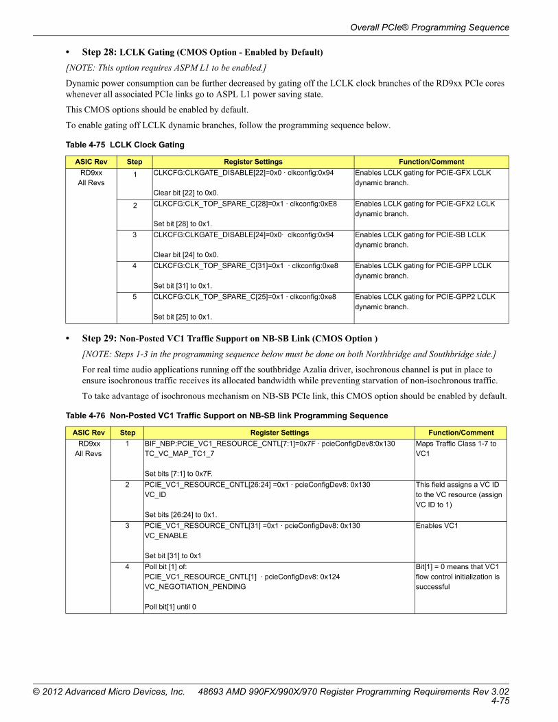
Overall PCIe® Programming Sequence
• Step 28: LCLK Gating (CMOS Option - Enabled by Default)
[NOTE: This option requires ASPM L1 to be enabled.]
Dynamic power consumption can be further decreased by gating off the LCLK clock branches of the RD9xx PCIe cores whenever all associated PCIe links go to ASPL L1 power saving state.
This CMOS options should be enabled by default.
To enable gating off LCLK dynamic branches, follow the programming sequence below.
• Step 29: Non-Posted VC1 Traffic Support on NB-SB Link (CMOS Option )
[NOTE: Steps 1-3 in the programming sequence below must be done on both Northbridge and Southbridge side.]
For real time audio applications running off the southbridge Azalia driver, isochronous channel is put in place to ensure isochronous traffic receives its allocated bandwidth while preventing starvation of non-isochronous traffic.
To take advantage of isochronous mechanism on NB-SB PCIe link, this CMOS option should be enabled by default.
Table 4-75 LCLK Clock Gating
ASIC Rev Step Register Settings Function/Comment
RD9xxAll Revs
1 CLKCFG:CLKGATE_DISABLE[22]=0x0 · clkconfig:0x94
Clear bit [22] to 0x0.
Enables LCLK gating for PCIE-GFX LCLK dynamic branch.
2 CLKCFG:CLK_TOP_SPARE_C[28]=0x1 · clkconfig:0xE8
Set bit [28] to 0x1.
Enables LCLK gating for PCIE-GFX2 LCLK dynamic branch.
3 CLKCFG:CLKGATE_DISABLE[24]=0x0· clkconfig:0x94
Clear bit [24] to 0x0.
Enables LCLK gating for PCIE-SB LCLK dynamic branch.
4 CLKCFG:CLK_TOP_SPARE_C[31]=0x1 · clkconfig:0xe8
Set bit [31] to 0x1.
Enables LCLK gating for PCIE-GPP LCLK dynamic branch.
5 CLKCFG:CLK_TOP_SPARE_C[25]=0x1 · clkconfig:0xe8
Set bit [25] to 0x1.
Enables LCLK gating for PCIE-GPP2 LCLK dynamic branch.
Table 4-76 Non-Posted VC1 Traffic Support on NB-SB link Programming Sequence
ASIC Rev Step Register Settings Function/Comment
RD9xxAll Revs
1 BIF_NBP:PCIE_VC1_RESOURCE_CNTL[7:1]=0x7F · pcieConfigDev8:0x130 TC_VC_MAP_TC1_7
Set bits [7:1] to 0x7F.
Maps Traffic Class 1-7 to VC1
2 PCIE_VC1_RESOURCE_CNTL[26:24] =0x1 · pcieConfigDev8: 0x130VC_ID
Set bits [26:24] to 0x1.
This field assigns a VC ID to the VC resource (assign VC ID to 1)
3 PCIE_VC1_RESOURCE_CNTL[31] =0x1 · pcieConfigDev8: 0x130VC_ENABLE
Set bit [31] to 0x1
Enables VC1
4 Poll bit [1] of:PCIE_VC1_RESOURCE_CNTL[1] · pcieConfigDev8: 0x124VC_NEGOTIATION_PENDING
Poll bit[1] until 0
Bit[1] = 0 means that VC1 flow control initialization is successful
© 2012 Advanced Micro Devices, Inc. 48693 AMD 990FX/990X/970 Register Programming Requirements Rev 3.024-75

Overall PCIe® Programming Sequence
4.4.8 PCIe® Workarounds
• Step 30: Workaround for Broadcom ASPM L1 Issue
Follow the programming sequence described in Section 4.4.8.1 ”Workaround for Broadcom 5709C ASPM L1 Issue” on page 4-76.
4.4.8.1 Workaround for Broadcom 5709C ASPM L1 Issue
The following programming sequence should be executed when system BIOS detects a Broadcom 5709C Device (Vendor ID: 0x14E4, Device ID: 0x1639) present in the system. This should be done for the root-complex PCIe port that thedevice is connected to.
Table 4-77 Broadcom 5709C Workaround
ASIC Rev Step Register Settings Function/Comment
N/A 1 BIF_NBP:PCIE_LC_TRAINING_CNTL[26]=0x0· PCIEIND_P:0xA1LC_RESET_ASPM_L1_NAK_TIMER
Clear bit [26] to 0x0.
For the device behind which the Broadcom 5709C is found, reset the 9.5us L1 Nak Counter if additional ASPM L1 requests received before counter finishes.
48693 AMD 990FX/990X/970 Register Programming Requirements Rev 3.02 © 2012 Advanced Micro Devices, Inc.4-76
Chapter 5HTIU Settings
5.1 HT Link Initialization
The RD9xx northbridge is expected to be the only HyperTransport™ device on the same HT chain with the processor. Moving the chipset off of unit ID 0 to look for additional devices, as described in various AMD processor BKDGs and the HyperTransport specification, is neither necessary, nor is it supported. All devices on PCI bus 0 are expected to be located within the northbridge and the southbridge. The use of a HyperTransport tunnel device between the processor and the RD9xx is not supported. If multiple northbridges are used, the ones not connected to the southbridge must be placed on separate logical PCI buses.
5.2 HTIU Indirect Register Space
Many non-standard HTIU related registers are located in an indirect register space HTIUNBIND. This is accessed through HTIU_NB_INDEX (with write-enable in bit [8], and index in bits [6:0]), and HTIU_NB_DATA in the NBCFG space. The location of the index/data pair is located in chipset primary bus number, device 0x0, function 0x0, registers 0x94 and 0x98.
5.3 CPU Register Access
5.3.1 Normal Registers
For a single-socket platform, the processor will be accessible through bus 0x0 device 0x18 with various function numbers. Note: In this document, these registers will be referred to as CPU_FX (where X stands for function number) x offset.
5.3.2 PHY Dataport Register Access
Refer to the section entitled “Link Phy Offset Registers (Function 4 registers 0x180, 188, 190, 198)” in the AMD family 10h processor BKDG to see how to program the processor HyperTransport PHY registers. Note: In the HTIU section of this document, these registers will be referred to as CPU_PHY 0xYY, where YY is the register offset.
The northbridge will always be connected to Link 0 so that CPU function 4 registers 0x180 and 0x184 will be used to control the PHY.
5.3.3 Link Dependent Registers
The processor supports multiple HyperTransport links, each of which can be coherent or non-coherent depending on system design. This document will focus on non-coherent link programming with respect to RD9xx. Some of the register settings will depend on specific link used to connect with RD9xx. To cover all the possible scenarios, registers that are link dependent will be shown according to this format: CPU F# x Link3_Offset/Link2_Offset/Link1_Offset/Link0_Offset
Please only program the appropriate link that is connected to the chipset.
5.4 Changing to High-Speed Mode
The HT link starts at 200MHz/8-bit mode on initial power-up. Software is responsible for reprogramming both the processor(s) and northbridge(s) for higher speed operation. Generating a warm reset will cause the system to restart using the new higher speeds.
5.4.1 Identifying Supported HT Frequencies
The HT frequency capability register located in NBCFG x D0[31:16] determines which HT frequencies are supported by the northbridge. The bits in this 16-bit register denote which frequency codes are valid. For example, a value of 0x25 indicates that frequency codes 0x0, 0x2, and 0x5 are valid indicating 200Mhz, 400Mhz, and 800Mhz support. Similarly, the HT frequency capability register in the processor is located in CPU_F0 x E8/C8/A8/88 bits [31:16] and are encoded in the same manner. Both the northbridge and the processor must be set to the same frequency. Note that the lower frequencies require HyperTransport 1 mode to operate while higher frequencies require HyperTransport 3 mode to operate.
© 2012 Advanced Micro Devices, Inc. 48693 AMD 990FX/990X/970 Register Programming Requirements Rev 3.025-1

Changing to High-Speed Mode
5.4.2 Changing to High-Speed HyperTransport™ 1 Mode
The following registers in Table 5-2 must be programmed to enable one of the high-speed HT1 modes.
Table 5-2Enabling High-Speed HT1 Modes
Table 5-1Identifying Supported HT Frequencies
HT Frequency Frequency Code IBIAS Comments
200Mhz 0x0 0x44 HyperTransport 1 only
400Mhz 0x2 0x44 HyperTransport 1 only
600Mhz 0x4 0xB6 HyperTransport 1 only
800Mhz 0x5 0x44 HyperTransport 1 only
1Ghz 0x6 0x96 HyperTransport 1 only
1.2Ghz 0x7 0xB6 HyperTransport 3 only
1.4Ghz 0x8 0x23 HyperTransport 3 only
1.6Ghz 0x9 0x44 HyperTransport 3 only
1.8Ghz 0xa 0x64 HyperTransport 3 only
2.0Ghz 0xb 0x96 HyperTransport 3 only
2.2Ghz 0xc 0xA6 HyperTransport 3 only
2.4Ghz 0xd 0xB6 HyperTransport 3 only
2.6Ghz 0xe 0xC6 HyperTransport 3 only
ASIC Rev Register Setting Function/Comment
RD9xx
All Revs
NBCFG x D0 [11:8] HT1 Frequency Code from Table 5-1
Sets HT Frequency in the chipset
NBCFG x C8 [26:24] 0x1 = 16 bit0x0 = 8 bit
Sets input HT link width on the chipset side to be 16-bit. Only 8-bit and 16-bit widths are supported.
NBCFG x C8 [30:28] 0x1 =16 bit0x0 = 8 bit
Sets output HT link width on the chipset side to be 16-bit. Only 8-bit and 16-bit widths are supported.
CLKCFG x D8 [9:0] IBIAS Code from Table 5-1 Sets the chipset HT PLL ibias setting
HTIUNBIND x 2A [1:0] 0x1 Optimize chipset HT transmitter drive strength
CPU_F0 x E8/C8/A8/88[11:8] HT1 Frequency Code from Table 5-1
Sets HT Frequency in the processor
CPU_F0 x E4/C4/A4/84 [26:24] 0x1 = 16 bit0x0 = 8 bit
Sets input HT link width on the processor side to be 16-bit. Only 8-bit and 16-bit widths are supported.
CPU_F0 x E4/C4/A4/84 [30:28] 0x1 = 16 bit0x0 = 8 bit
Sets output HT link width on the processor side to be 16-bit. Only 8-bit and 16-bit widths are supported.
Note: Once these registers are programmed, a warm-reset must be performed to switch to high-speed mode.
48693 AMD 990FX/990X/970 Register Programming Requirements Rev 3.02 © 2012 Advanced Micro Devices, Inc.5-2

Changing to High-Speed Mode
5.4.3 Changing to HyperTransport™ 3 Mode
HyperTransport 3 capability in the northbridge can be detected by searching the PCI capability linked list for a header with Capability_ID 0x8 and Capability_Type 0xD0. Assuming the processor is HyperTransport 3 capable, HyperTransport 3 modes can be enabled by programming the following registers in Table 5-3. This can be done directly from the 200Mhz/8-bit bootup mode. Please note that to program HT3 capability registers properly, NBCFG x 9c[17:16] must be set to 0x0.
Table 5-3RD9xx Register Settings for HyperTransport 3 Mode
ASIC Rev Register Setting Function/Comment
RD9xx
All Revs
NBCFG x D0 [11:8] HT3 Frequency Code from Table 5-1
Sets HT Frequency in the chipset
NBCFG x C8 [26:24] 0x1 = 16 bit0x0 = 8 bit
Sets input HT link width on the chipset side to be 16-bit. Only 8-bit and 16-bit widths are supported
NBCFG x C8 [30:28] 0x1 = 16 bit0x0 = 8 bit
Sets output HT link width on the chipset side to be 16-bit. Only 8-bit and 16-bit widths are supported
CLKCFG x D8 [9:0] IBIAS Code from Table 5-1 Sets the chipset HT PLL IBIAS setting
NBCFG x 44 [0] 0x1 Enables error-retry mode
NBCFG x AC [3] 0x1 Enables scrambling
NBCFG x A4 [31] 0x1 Enables transmitter de-emphasis
NBCFG x A4 [26:24] See Function/Comment. Enables transmitter de-emphasis levelThis depends on the PCB design and the trace length between NB and processorUse 0x4 for bringup.See section 5.5.6 (transmitter de-emphasis) for programming guidelines.
NBCFG x A0 [5:0] LS0 = 0usLS1 = 2us
LS2 = CPU_PHY x [530A,520A] [Ls2ExitTime] + 2us
Sets Training 0 time. These settings are chosen to match the processor requirements. See Table 5-5 for encodings
NBCFG x AC [14] 0x1 Disables command throttling
HTIUNBIND x 15 [22] 0x1 Enables strict TM4 detection
HTIUNBIND x 2A [1:0] 0x1 Optimizes chipset HT transmitter drive strength
Table 5-4CPU Register Settings for HyperTransport 3
ASIC Rev Register Setting Function/Comment
RD9xx
All Revs
CPU_F0 x E8/C8/A8/88[11:8] HT3 Frequency Code from Table 5-1
Sets HT Frequency in the processor.
CPU_F0 x E4/C4/A4/84[26:24] 0x1 Sets input HT link width on the processor side to be
16-bits.CPU_F0 x E4/C4/A4/84[30:28] 0x1 Sets output HT link width on the processor side to be
16-bits.CPU_F0 x 13C/138/134/130[0] 0x1 Enables error-retry mode.CPU_F0 x 17C/178/174/170[3] 0x1 Enables scrambling.
CPU_PHY x C5 See Function/Comment Enables transmitter de-emphasis.
This depends on the PCB design and the trace length
between NB and processor.
For bringup, use the -3dB settings described in the
appropriate processor BKDG (for Family 10h, this is
located under “Link PHY De-emphasis Value
Registers”).
This register is also link dependent.
© 2012 Advanced Micro Devices, Inc. 48693 AMD 990FX/990X/970 Register Programming Requirements Rev 3.025-3
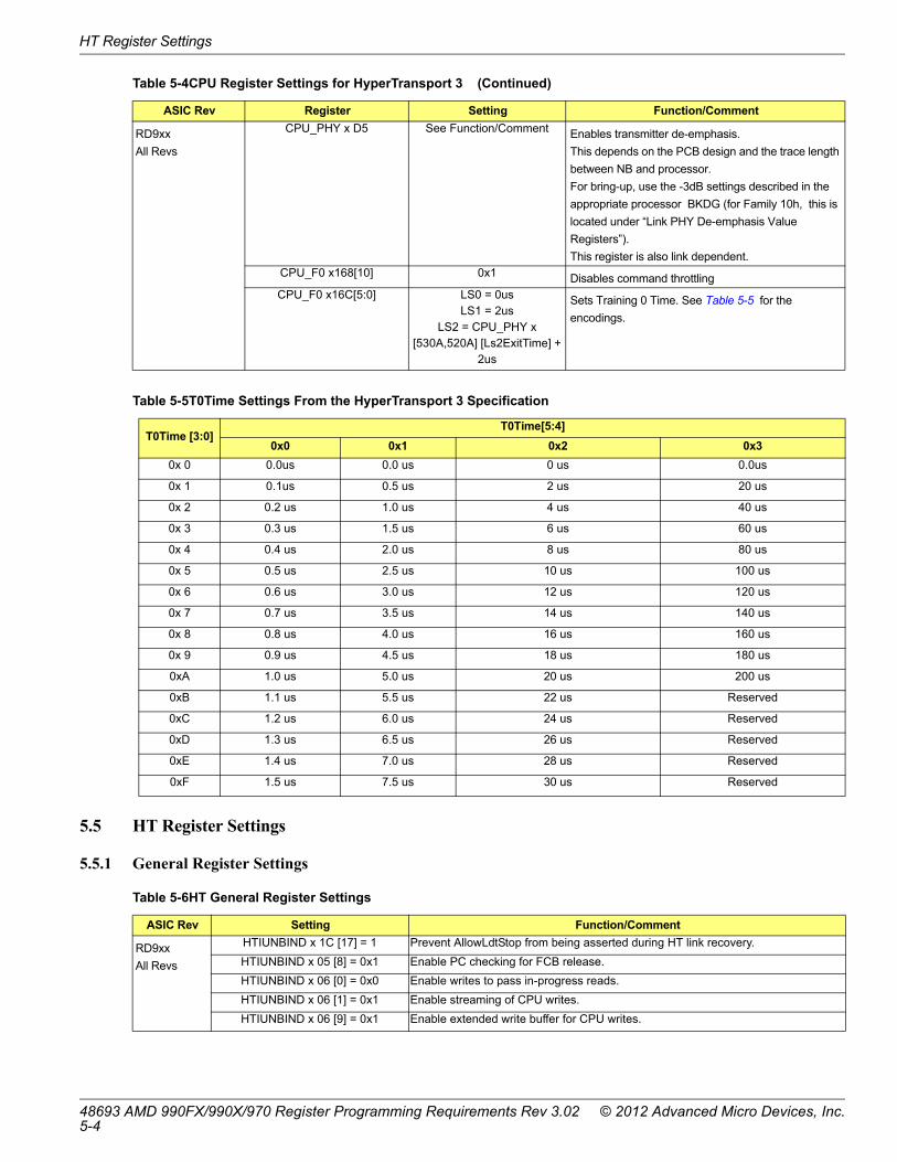
HT Register Settings
Table 5-5T0Time Settings From the HyperTransport 3 Specification
5.5 HT Register Settings
5.5.1 General Register Settings
RD9xx
All Revs
CPU_PHY x D5 See Function/Comment Enables transmitter de-emphasis.
This depends on the PCB design and the trace length
between NB and processor.
For bring-up, use the -3dB settings described in the
appropriate processor BKDG (for Family 10h, this is
located under “Link PHY De-emphasis Value
Registers”).
This register is also link dependent.CPU_F0 x168[10] 0x1 Disables command throttlingCPU_F0 x16C[5:0] LS0 = 0us
LS1 = 2usLS2 = CPU_PHY x
[530A,520A] [Ls2ExitTime] + 2us
Sets Training 0 Time. See Table 5-5 for the
encodings.
T0Time [3:0]T0Time[5:4]
0x0 0x1 0x2 0x3
0x 0 0.0us 0.0 us 0 us 0.0us
0x 1 0.1us 0.5 us 2 us 20 us
0x 2 0.2 us 1.0 us 4 us 40 us
0x 3 0.3 us 1.5 us 6 us 60 us
0x 4 0.4 us 2.0 us 8 us 80 us
0x 5 0.5 us 2.5 us 10 us 100 us
0x 6 0.6 us 3.0 us 12 us 120 us
0x 7 0.7 us 3.5 us 14 us 140 us
0x 8 0.8 us 4.0 us 16 us 160 us
0x 9 0.9 us 4.5 us 18 us 180 us
0xA 1.0 us 5.0 us 20 us 200 us
0xB 1.1 us 5.5 us 22 us Reserved
0xC 1.2 us 6.0 us 24 us Reserved
0xD 1.3 us 6.5 us 26 us Reserved
0xE 1.4 us 7.0 us 28 us Reserved
0xF 1.5 us 7.5 us 30 us Reserved
Table 5-6HT General Register Settings
ASIC Rev Setting Function/Comment
RD9xx
All Revs
HTIUNBIND x 1C [17] = 1 Prevent AllowLdtStop from being asserted during HT link recovery.
HTIUNBIND x 05 [8] = 0x1 Enable PC checking for FCB release.
HTIUNBIND x 06 [0] = 0x0 Enable writes to pass in-progress reads.
HTIUNBIND x 06 [1] = 0x1 Enable streaming of CPU writes.
HTIUNBIND x 06 [9] = 0x1 Enable extended write buffer for CPU writes.
Table 5-4CPU Register Settings for HyperTransport 3 (Continued)
ASIC Rev Register Setting Function/Comment
48693 AMD 990FX/990X/970 Register Programming Requirements Rev 3.02 © 2012 Advanced Micro Devices, Inc.5-4

HT Register Settings
RD9xx
All Revs
HTIUNBIND x 06 [13] = 0x1 Enable additional response buffers.
HTIUNBIND x 06 [17] = 0x1 Enable special reads to pass writes.
HTIUNBIND x 06 [16:15] = 0x3 Enable decoding of C1e/C3 and FID cycles.
HTIUNBIND x 06 [25] = 0x1 Enable HTIU-display handshake bypass.
HTIUNBIND x 06 [30] = 0x1 Enable tagging fix.
HTIUNBIND x 07 [0] = 0x1 Enable byte-write optimization for IOC requests.
HTIUNBIND x 07 [1] = 0x0 Disable delaying STPCLK de-assert during FID sequence.
HTIUNBIND x 07 [2] = 0x0 Disable upstream system-management delay.
HTIUNBIND x 16 [11] = 0x1 Enable transmit PHY to reinitialize in HT1 mode when tristate is enabled
HTIUNBIND x 1D [2] = 0x0 Enable datarate matching circuitry in the chipset
HTIUNBIND x 1D [4] = 0x0 Enable sync flood detection in the chipset
The following 4 register settings are designed to avoid DMA Deadlock. Program these registers in the order they are listed. Also, any LPC memory-mapped regions must not be covered by one of the CPU’s MMIO ranges. This includes ROM space addresses that may be accessed during SBIOS flashing routines.
CPU_F0 R68[22:21] = 0x0 No limit for NP transactions
SB AXINDC x 10 [9] = 0x1 Enable special NP protocol in the southbridge PCIE.
SB PCIEIND x 10 [9] = 0x1 Enable special NP protocol in the northbridge PCIE port attached to the southbridge.
HTIUNBIND x 06 [26] = 1 Enable special NP protocol in HTIU.
HTIUNBIND x 16 [10] = 1 Enable proper DLL reset sequence.
HTIUNBIND x 2B [31:28] = 0xF Enable BIAS circuit for all lanes.
HTIUNBIND x 0C [15:0] = 0x101 Change GCM WRR to burst length of 1 for performance
RD9xx
Rev A21
HTIUNBIND x 5 [3] = 0x1 Generate Disconnect Nop without credit release
HTIUNBIND x 5 [4] = 0x1 Reduce HT1 LDTSTOP disconnect delay
HTIUNBIND x 5 [6] = 0x1 Prevent false error logging due to reset skew
HTIUNBIND x 5 [10] = 0x1 Fix Data Rate Matching feature for 16 bit link
HTIUNBIND x 5 [12] = 0x1 Allow DMA P request to pass NP request
HTIUNBIND x 5 [13] = 0x1 Enable earlier CDR freeze prior to disconnect
HTIUNBIND x 5 [14] = 0x1 Enhance error detection during training2
HTIUNBIND x 5 [15] = 0x1 Enable proper parity error reporting for IOMMU L2A and L2B
HTIUNBIND x 5 [16] = 0x1 Prevent Nop insertion in extended address command in HT1
HTIUNBIND x 5 [17] = 0x1 Enable proper handling of 64 bit register access to IOMMU/IOAPIC space
HTIUNBIND x 5 [18] = 0x1 Reduce false retry reporting due to LDTSTOP disconnect
HTIUNBIND x 5 [19] = 0x1 Improve power reduction during link disconnect
Table 5-6HT General Register Settings (Continued)
ASIC Rev Setting Function/Comment
© 2012 Advanced Micro Devices, Inc. 48693 AMD 990FX/990X/970 Register Programming Requirements Rev 3.025-5

HT Register Settings
5.5.2 UnitID Clumping
The RD9xx supports UnitID clumping to increase the number of outstanding requests supported by a single device. Clumping is supported in Family 10h processors. It may be enabled for PCI-Express GFX links when using only the lower number bridge within each PCI-Express® GFX core. For example, when using bridge 2, and not bridge 3 (UnitIDs 0x2 and 0x3), to support a single x8 or x16 PCI-Express link, the UnitIDs reserved for both bridges may be clumped together. Clumping may also be used with bridges 11 and 12 (UnitIDs 0xB and 0xC). The clumping register must be enabled the same in both the chipset and processor.
NOTE: If the unused/empty bridge is designed as a hot-plug slot, then clumping should be disabled.
Table 5-7Register Settings for UnitID Clumping
UnitID Clumping options in the SBIOS menu should be as follows:
• UnitID Clumping Disabled (default)• Clump UnitIDs 0x2 + 0x3 and 0xB + 0xC• Clump UnitIDs 0x2 + 0x3• Clump UnitIDs 0xB + 0xC
If a particular pair of UnitIDs cannot be clumped because they do not meet the criteria described above, then clumping should not be enabled, regardless of the menu selection.
ASIC Rev Register Setting Function/Comments
RD9xx All
Revs
NBCFG x 5C [3] 0x1 Enables clumping of UnitIDs 2 and 3.
CPU_F0 x 11C/118/114/110 [3] 0x1 Enables clumping of UnitIDs 2 and 3 in family 10h processors.
NBCFG x 5C [12] 0x1 Enables clumping of UnitIDs 0xB and 0xC.
CPU_F0 x 11C/118/114/110 [12] 0x1 Enables clumping of UnitIDs 0xB and 0xC in family 10h processors.
Note: These registers take effect immediately. Clumping registers are cleared on warm-reset and should be programmed before DMA traffic
is enabled. CPU programming depends on the link that the chipset is connected to.
48693 AMD 990FX/990X/970 Register Programming Requirements Rev 3.02 © 2012 Advanced Micro Devices, Inc.5-6

HT Register Settings
5.5.3 Isochronous Flow-Control Mode
The RD9xx supports the use of the Isochronous Flow-Control Mode (IFCM) function to provide reduced latency and avoid deadlocks for IOMMU table walker requests. In this mode, dedicated flow-control buffering must be reserved inside of the processor. Refer to the register settings in section 5.5.4 to reserve the isochronous flow-control buffers along with the appropriate processor BKDG. In addition to this, the isochronous mode must be enabled.
Table 5-8Register Settings for Enabling Isochronous Flow-Control Mode
If isochronous flow-control mode is not enabled, the legacy display refresh mode should be enabled.
Table 5-9Register Settings for Enabling Display-Refresh in Normal Flow Control Mode
5.5.4 Family 10h Processor Buffer Allocation Settings
This section only covers buffer allocation for Non-Coherent link. Please refer to Family 10h BKDG for Coherent link buffer allocation. The settings below are based on register definition for Family 10h Rev C processor.
Definitions:
Sublink – A group of 8 consecutive HyperTransport lanes, also called byte lane.
Ganged – When two sublinks work together and act as one 16-bit HT link. Most client systems or single NB platforms use Ganged HT link between processor and NB.
Unganged – When sublink connects individually and act as two separate 8-bit HT link. In certain server configurations with multiple NB, the HT link between processor and NB might be Unganged.
Non-Coherent link – This refers to HT link between processor and NB.
Coherent link – This refers to HT link between processor and processor.
NFCM – Normal Flow Control Mode.
IFCM – Isochronous Flow Control Mode.
5.5.4.1 HT Buffer Allocation for Ganged Links
ASIC Rev Register Setting Function/Comments
RD9xx All
Revs
NBCFG x C8 [12] 0x1 Enables IFCM in the chipset.
CPU_F0 x E4/C4/A4/84 [12] 0x1 if Link 1 is connected to RD9xx; 0x0 otherwise
Enables IFCM on the link between processor and chipset.
ASIC Rev Register Setting Function/Comments
RD9xx All Revs CPU F0 x 68 [24] 0x1 Enables Display Refresh Mode in the processor. This setting applies to family 10h
processors. This bit takes effect immediately. Please set it after the warm reset is
used to make changes to HyperTransport and processor XBAR/XCS buffer
allocations take effect.
Table 5-10HT Buffer Allocation for Ganged, Non-Coherent Links and Normal Flow-Control Mode
ASIC Rev Register Setting Function/Comments
RD9xx All
Revs
CPU_F0 x F0/D0/B0/90 [27:25] 0x1 2 Free Data
CPU_F0 x F0/D0/B0/90 [24:20] 0x8 16 Free Commands
CPU_F0 x F0/D0/B0/90 [19:18] 0x1 2 Response Data
CPU_F0 x F0/D0/B0/90 [17:16] 0x0 0 Non-posted Data
CPU_F0 x F0/D0/B0/90 [15:12] 0x0 0 Probe Commands
CPU_F0 x F0/D0/B0/90 [11:8] 0x1 2 Response Commands
CPU_F0 x F0/D0/B0/90 [7:5] 0x6 12 Posted Command and 12 Posted Data
CPU_F0 x F0/D0/B0/90 [4:0] 0x11 34 Non-posted Commands
Note: These registers require a warm reset to take effect.
© 2012 Advanced Micro Devices, Inc. 48693 AMD 990FX/990X/970 Register Programming Requirements Rev 3.025-7

HT Register Settings
Table 5-11HT Buffer Allocation for Ganged, Non-Coherent Links and Isochronous Flow-Control Mode
5.5.4.2 XBAR/XCS Buffer Allocation
All XBAR/XCS buffer allocation settings should follow the recommendations in the appropriate processor family BKDG. The single-link processor settings should be used.
ASIC Rev Register Setting Function/Comments
RD9xx All
Revs
CPU_F0 x F0/D0/B0/90 [27:25] 0x1 2 Free Data
CPU_F0 x F0/D0/B0/90 [24:20] 0x8 16 Free Commands
CPU_F0 x F0/D0/B0/90 [19:18] 0x1 2 Response Data
CPU_F0 x F0/D0/B0/90 [17:16] 0x0 0 Non-posted Data
CPU_F0 x F0/D0/B0/90 [15:12] 0x0 0 Probe Commands
CPU_F0 x F0/D0/B0/90 [11:8] 0x1 2 Response Commands
CPU_F0 x F0/D0/B0/90 [7:5] 0x6 12 Posted Commands and 12 Posted Data
CPU_F0 x F0/D0/B0/90 [4:0] 0xF 30 Non-posted Commands
CPU_F0 x F4/D4/B4/94 [18:16] 0x2 4 Isochronous Non-posted Commands
Note: These registers require a warm reset to take effect.
48693 AMD 990FX/990X/970 Register Programming Requirements Rev 3.02 © 2012 Advanced Micro Devices, Inc.5-8
HT Register Settings
5.5.5 HyperTransportTM Protocol Checker
In any HyperTransport mode, the RD9xx can perform basic checks on the HyperTransport protocol in order to detect errors separately from the periodic CRC or per-packet CRC mechanism.
Table 5-12Register Settings for HT Protocol Checker
5.5.6 Transmitter De-emphasis
The following table contains guidelines on how to set the RD9xx HT transmitter de-emphasis level. These are a starting point and adjustments may be necessary to optimize for a specific platform implementation. The de-emphasis level is programmed through NBCFG x A4 [26:24].
Table 5-13Transmitter De-Emphasis Versus Trace Length
5.5.7 Low-Power HyperTransportTM Features
5.5.7.1 HyperTransport 1
In HyperTransport 1 mode, the RD9xx can tristate parts of the link in order to reduce power consumption. By default, no lanes are tristated. The CAD and CTL lanes may be tristated together or CAD, CTL, and CLK may be tristated.
Table 5-14Register Settings for Tristating CAD and CTL
Table 5-15Register Settings for Tristating CAD, CTL and CLK
5.5.7.2 HyperTransport 3
In HyperTransport 3 mode, the RD9xx supports the LS1 and the LS2 low-power states when LDTSTOP# is asserted, programmable through the LSSel register. The system must enable either the LS1 or the LS2 low power states. The LS1 features low reconnection latency but higher power consumption relative to the LS2.
ASIC Rev Register Setting Function/Comments
RD9xx All Revs
HTIUNBIND x 1E [31:0] 0x7FFF_FFFC Enables the HyperTransport protocol checker in the chipset.
ASIC Rev Trace Length De-Emphasis Level De-Emphasis Code
RD9xx All Revs 0 to 4.5” -1.32dB 0x1
4.5” to 8” -2.08dB 0x2
8” to 11” -3.1dB 0x3
11” to 14” -4.22dB 0x4
14” to 18” -5.50dB 0x5
18+” -7.05dB 0x6
18+” -9.0dB 0x7 *
* This setting may be useful for extremely long or lossy channels.
ASIC Rev Register Setting Function/Comments
RD9xx All Revs
NBCFG x C8 [13] 0x1 Enables HT Tristate in the chipset
NBCFG x AC [8] 0x0 Disables HT CLK Tristate in the chipset
CPU_F0 x E4/C4/A4/84 [13] 0x1 Enables HT Tristate in the CPU
CPU_F0 x 17C/178/174/170 [8] 0x0 Disables HT CLK Tristate in the CPU
ASIC Rev Register Setting Function/Comments
RD9xx All Revs
NBCFG x C8 [13] 0x1 Enables HT Tristate in the chipset.
NBCFG x AC [8] 0x1 Enables HT CLK Tristate in the chipset.
CPU_F0 x E4/C4/A4/84 [13] 0x1 Enables HT Tristate in the CPU.
CPU_F0 x 17C/178/174/170 [8] 0x1 Enables HT CLK Tristate in the CPU.
CPU F3 x D8 [27:24] 0x3 Reconnects the Delay Timer in the CPU.
© 2012 Advanced Micro Devices, Inc. 48693 AMD 990FX/990X/970 Register Programming Requirements Rev 3.025-9

HT Register Settings
Table 5-16Register Settings for LS1
Table 5-17Register Settings for LS2
5.5.7.3 Inactive Lane State
When the HT link width is reduced below 16 bits in either direction, the electrical state of the inactive lanes will be controlled by the Inactive Lane State register. The chipset inactive lane state register setting is based on the values programmed in the processor as per the following table.
5.5.7.4 Generalized Stutter Mode
Generalized Stutter Mode (GSM) must be enabled when enabling the C1e low power state in the processor. This feature allows the chipset to reconnect the Hypertransport link when the processor is in the C1e state in order to pass DMA requests to memory.
Table 5-19Register Settings for GSM
ASIC Rev Register Setting Function/Comments
RD9xx All Revs NBCFG x AC [8:7] 0x0 Enables LS1 in the chipset.
CPU_F0 x 17C/178/174/170 [8] 0x0 Enables LS1 in the Family 10h CPU.
ASIC Rev Register Setting Function/Comments
RD9xx All Revs NBCFG x AC [8:7] 0x2 Enables LS2 in the chipset.
HTIUNBIND x 15 [27] 0x1 Powers down the chipset DLLs in the LS2 state.
CPU_F0 x 17C/178/174/170 [8] 0x1 Enables LS2 in the Family 10h CPU.
Table 5-18Register Settings for HT1 and HT3 Inactive Lane State
ASIC Rev HT Mode and LS State
Processor InLnSt Setting
CPU_F0 x 16C [7:6]
Program chipset InLnSt Register
NBCFG x A0 [7:6]
Function/Comments
RD9xx All Revs
8-bit HT link (HT1 or HT3)
Any 0x1 Place the upper half of the HT PHY into the PHY_OFF state to maximize power savings. Processor side of the link should be off via processor TransOff and EndofChain register bits.
HT1 and 16-bit HT link 0x0 0x0 Warm reset signalling
0x1 0x1 PHY_OFF state
0x2 0x2 Operational signaling
0x3 0x3 Tristate
HT3 LS1 and 16-bit HT link
0x0 0x0 Warm reset signalling
0x1 0x0 Do not enable HT3 LS1 with InLnSt=0x1 (PHY_OFF) as per errata 9.
0x2 0x2 Operational signaling
0x3 0x3 LS1 disconnected state
HT3 LS2 and 16-bit HT link
0x0 0x0 Warm reset signaling
0x1 0x1 PHY_OFF state
0x2 0x2 Operational signaling
0x3 0x3 LS2 disconnected state
ASIC Rev Register Setting Function/Comments
RD9xx All Revs NBMISCIND x C [13] 0x1 Enables GSM Mode.
HTIUNBIND x 1C [31:17] 0xFFF Enables all traffic to be detected as GSM traffic.
48693 AMD 990FX/990X/970 Register Programming Requirements Rev 3.02 © 2012 Advanced Micro Devices, Inc.5-10

Chapter 6IOAPIC
This chapter discusses the IOAPIC registers, initialization and feature programming. The IOAPIC can improve system performance significantly by delivering the interrupts to the system quickly and exposing more unique interrupt vectors. IOAPIC is only used for legacy interrupts and it is not used for MSI based interrupts.
6.1 IOAPIC Register Spaces
Figure 6-1 IOAPIC Register Spaces
Four register spaces are involved in the IOAPIC block:
• Northbridge configuration space (NBCFG)
• IOAPIC configuration registers space - indirect
• Direct memory mapped registers space
NBCONFIG Configuration Space
___________________________
___________________________INDEX
___________________________DATA
IOAPIC Configuration Space
_________________________Feature Enable Register
_________________________BAR (Lower Base Address)
_________________________BAR (Upper Base Address)
_________________________Interrupt routing table
_________________________Interrupt routing table
_________________________
_________________________
Register Set #1 Configuration Space Registers
Register Set #2 Direct Memory Mapped Registers
IOAPIC Memory Mapped Registers
___________________________Index Register
___________________________Window Register
___________________________IRQ (PAR) Pin Assertion Register___________________________
EOI Register
IOAPIC Indirect Address Registers
_________________________IOAPIC ID Register
_________________________IOAPIC Version Register
_________________________Interrupt redirect table entry 0
_________________________Interrupt redirect table entry 1
_________________________Interrupt redirect table entry 2
_________________________…...
_________________________Interrupt redirect table entry 31
© 2012 Advanced Micro Devices, Inc. 48693 AMD 990FX/990X/970 Register Programming Requirements Rev 3.026-1

IOAPIC Register Spaces
• Indirect memory mapped registers space.
6.1.1 IOAPIC Registers in the NBCFG Space
The Northbridge Configuration space has 2 registers - Index and Data. These allow the user to access the IOAPIC Configuration space.
6.1.2 IOAPIC Configuration Registers Space
This configuration space deals with the basic features and controls of the IOAPIC. This register space also allows the user to set the base address for the memory mapped registers. The Memory Mapped register space cannot be accessed until the Base Address Register (BAR) is defined. (Note: BAR is made up of two registers - IOAPIC_Conf_Lower and IOAPIC_Conf_Upper.)
Note: The XAPIC_BASE_REGISTER has a power-on default value of FEC0_0000H.
6.1.3 IOAPIC Direct Memory Mapped Registers Space
Once the BAR register has been written in the IOAPIC Configuration space, these memory mapped registers become accessible. There are 4 direct registers in the memory mapped register space:
• IO Register Select – Allows access to the indirect registers in the memory mapped space. Bits 7-0 indicate the addresses of the indirect registers, the rest are reserved.
Table 6-1 IOAPIC Registers in the NBCFG Space
Register Address in NBCFG Space Description
INDEX 0xF8 Address of the IOAPIC’s indirect configuration space register
DATA0xFC Data to be written at the address
Table 6-2 IOAPIC Configuration BAR Registers
ASIC Rev RegisterAddress in IOAPIC
Configuration SpaceBits Field Name Description
RD9xx All Revs IOAPIC_Conf_Lower 0x01 2:0 Reserved Reserved
3 Mem_IO_Map Base Address Mapping1: Memory Map0: IO Map(Set to 1 by default)
4 Reserved Reserved
31:5 IOAPIC_Addr Base Address for IOAPIC (default to FEC000xx)
IOAPIC_Conf_Upper 0x02 31:0 IOAPIC_Addr_Upper Base Address for IOAPIC (default to FEC000xx)
Table 6-3 1-3 IOAPIC Memory Mapped Registers
Asic Rev RegisterAddress in IOAPIC Direct Memory Mapped Space
Bits Field Name Description
RD9xx All Revs
IO_Register_Select_Index
BAR register + 0x00 7:0 Indirect_Address_Offset
Indirect Address Offset
31:8 Reserved
IO_Window_Register BAR register + 0x10 31:0 Window Data to be written to the register selected by the indirect address offset
IRQ_PIN_ASSERTION_REGISTER
BAR register + 0x20 7:0 Input_IRQ Write Only. IRQ number for the requested interrupt
31:8 Reserved
EOI_REGISTER BAR register + 0x20 7:0 Vector Write Only. Interrupt vector
31:8 Reserved
48693 AMD 990FX/990X/970 Register Programming Requirements Rev 3.02 © 2012 Advanced Micro Devices, Inc.6-2

IOAPIC Operation
• IO Window Register – Allows data to be written to the indirect registers. This is a 32 bit register. The Select and Window registers are used together to access the indirect registers.
• IRQ PIN Assertion – Writing to this register causes the IOAPIC to generate an interrupt. Any number between 0 and 31/23 can be written to this register and the IOAPIC will generate that particular interrupt. Only bits 7-0 can be used while the reset are reserved.
• EOI Register – For level sensitive interrupts, the CPU needs to indicate to the IOAPIC that the interrupt has been serviced. The IOAPIC will keep the corresponding remote IRR bit high until it receives such a message. The CPU can send this EOI message in 2 ways: It can either send an EOI broadcast message over HyperTransport™, or it can write to the EOI register. The CPU must not try to create a collision by clearing one level sensitive interrupt using a broadcast message and clearing a second level sensitive interrupt by writing to this register at the same time. The CPU must make sure that while it is sending a broadcast message it does not write to this register.
6.1.4 IOAPIC Indirect Memory Mapped Registers Space
The first 3 memory mapped indirect registers are: IOAPIC ID, IOXAPIC Version, and IOAPIC Arbitration.
6.2 IOAPIC Operation
The following steps are required to operate the IOAPIC:
1) Write the Base Address Register (BAR), see section 6.1: “IOAPIC Configuration Registers Space” on page 6-2. Note: BAR has a power-on default value of FEC0_00xx.
2) Write to the IOAPIC Features Enable register (see Table 6-5), which performs the following:
• Switches on IOAPIC
• Sets the number of interrupts entries inside IOAPIC (32 or 24)
• Allows the IOAPIC to send “wake” signals to the IOC, upon interrupt generation.
• Switches on the southbridge feature, which allows masked interrupt entries to be routed to the southbridge.
Table 6-4 IOAPIC Indirect Memory Mapped Registers
ASIC Rev RegisterAddress in IOAPIC Indirect
Memory Mapped SpaceBits Field Name Description
RD9xx All Revs
IOAPIC_ID_REGISTER 0x00 23:0 Reserved
27:24 ID IOAPIC device ID for APIC serial bus delivery mode. Read Only.
31:28 Extended ID Extended IOAPIC device ID for APIC serial bus delivery mode, if the Ioapic_id_ext_en is set to 1. Read Only
IOAPIC_VERSION_REGISTER
0x01 7:0 Version PCI 2.2 compliant. This register has a default value of hx21. Read Only
14:8 Reserved
15 PRQ IRQ pin assertion supported. Default value for this bit is 1. Read Only.
23:16 Max Redirection Entries
Defaults to 23 entries – This register show the number of entries minus 1. If the Ioapic_entrees bit in the Features_Enable register is set to 1, the value in this register will be 31. Read Only
31:24 Reserved
IOAPIC_ARBITRATION_REGISTER
0x02 23:0 Reserved
27:24 Arbitration_ID Arbitration ID for APIC serial bus delivery mode. Not supported. The Arbitration register is not supported as there is no longer a discrete APIC bus.
31:28 Reserved
© 2012 Advanced Micro Devices, Inc. 48693 AMD 990FX/990X/970 Register Programming Requirements Rev 3.026-3
IOAPIC Operation
3) Write to the remaining interrupt routing registers. Configure the interrupt routing which routes the 58 incoming interrupts to 32 or 24 interrupt depending on the mode (see section 6.3: “Setting Interrupts” on page 6-5). A recommended configuration is shown below:
4) Write to the redirection table entrees in the memory mapped space Enable/disable interrupts using the mask bits, assign vectors, destination ID, trigger modes for each of the 32 or 24 interrupts (see section 6.5: “Redirection Table Entry Registers” on page 6-15).
Table 6-5 IOAPIC Features Enable Register
ASIC Rev RegisterAddress in IOAPIC
Configuration SpaceBits Field Name Description
RD9xx All Revs
Features_enable 0x00 0 Ioapic_enable When set, this block will decode ioapic address
1 Ioapic_entries 1 = 32 entry IOAPIC0 = 24 entry IOAPIC
2 Ioapic_id_ext_en Extend IOAPIC ID from 4-bit to 8-bit
3 Ioapic_c2wake_en Generate C2Wake messages to the IOC
4 Ioapic_sb_feature_en Allows masked interrupts to be re-routed back to the south bridge PIC/IOAPIC
Table 6-6 Recommended Interrupt Routing Configuration
Device IOAPIC Mapped Group Swizzling Device’s Bridge PIN Mapping
HT 31
IOMMU 31
Device 2 0 ABCD 28
Device 3 1 ABCD 28
Device 4 5 ABCD 28
Device 5 5 CDAB 28
Device 6 6 BCDA 29
Device 7 6 CDAB 29
Device 9 6 ABCD 29
Device 10 5 BCDA 30
Device 11 2 ABCD 30
Device 12 3 ABCD 30
Device 13 4 ABCD 30
48693 AMD 990FX/990X/970 Register Programming Requirements Rev 3.02 © 2012 Advanced Micro Devices, Inc.6-4

Setting Interrupts
6.3 Setting Interrupts
The IOAPIC has a total of 58 interrupt inputs. These 58 interrupts are mapped to either 32 or 24 interrupt entries depending on the mode selected in the Features Enable register. There are 11 groups of interrupts, each group having a 4 interrupt bus (INT A, B, C, D). This gives a total of 44 interrupts coming from groups. The remaining 14 interrupts are single bit interrupts (see section 6.3: “Individual Interrupt Routing” on page 6-8). The Group Interrupt Routing registers, shown below, deal with all 11 groups and the 14 individual interrupts. Each group is assigned a output group number and a swizzle number. Individual bits are assigned an output pin number.
6.3.1 Group Interrupt Routing Registers
Table 6-7 IOAPIC Interrupt Routing Register 1
ASIC Rev Register
Address in IOAPIC
Configuration Space
Field Name Bits Description
RD9xx All Revs
IOAPIC_Int_routing_register_1
0x03 D2ext_Intr_grp 2:0 Map D2 external INTA/B/C/D to IOAPIC pins [(grp*4):(grp-1)*4]
D2ext_Intr_swz 5:4 Swizzle D2 external INT A/B/C/D based on the value in this register before mapping them onto the IOAPIC pins0 – ABCD1 – BCDA2 – CDAB3 – DABC
D3ext_Intr_grp 10:8 Map D3 external INTA/B/C/D to IOAPIC pins [(grp*4):(grp-1)*4]
D3ext_Intr_swz 13:12 Swizzle D3 external INT A/B/C/D based on the value in this register before mapping them onto the IOAPIC pins0 – ABCD1 – BCDA2 – CDAB3 – DABC
D4ext_Intr_grp 18:16 Map D4 external INTA/B/C/D to IOAPIC pins [(grp*4):(grp-1)*4]
D4ext_Intr_swz 21:20 Swizzle D4 external INT A/B/C/D based on the value in this register before mapping them onto the IOAPIC pins0 – ABCD1 – BCDA2 – CDAB3 – DABC
D5ext_Intr_grp 26:24 Map D5 external INTA/B/C/D to IOAPIC pins [(grp*4):(grp-1)*4]
D5ext_Intr_swz 29:28 Swizzle D5 external INT A/B/C/D based on the value in this register before mapping them onto the IOAPIC pins0 – ABCD1 – BCDA2 – CDAB3 – DABC
© 2012 Advanced Micro Devices, Inc. 48693 AMD 990FX/990X/970 Register Programming Requirements Rev 3.026-5

Setting Interrupts
Table 6-8 IOAPIC Interrupt Routing Register 2
ASIC Rev Register
Address in IOAPIC
Configuration Space
Field Name Bits Description
RD9xx All Revs
IOAPIC_Int_routing_register_2
0x04 D6ext_Intr_grp 2:0 Map D6 external INTA/B/C/D to IOAPIC pins [(grp*4):(grp-1)*4]
D6ext_Intr_swz 5:4 Swizzle D6 external INT A/B/C/D based on the value in this register before mapping them onto the IOAPIC pins0 – ABCD1 – BCDA2 – CDAB3 – DABC
D7ext_Intr_grp 10:8 Map D7 external INTA/B/C/D to IOAPIC pins [(grp*4):(grp-1)*4]
D7ext_Intr_swz 13:12 Swizzle D7 external INT A/B/C/D based on the value in this register before mapping them onto the IOAPIC pins0 – ABCD1 – BCDA2 – CDAB3 – DABC
D9ext_Intr_grp 18:16 Map D9 external INTA/B/C/D to IOAPIC pins [(grp*4):(grp-1)*4]
D9ext_Intr_swz 21:20 Swizzle D9 external INT A/B/C/D based on the value in this register before mapping them onto the IOAPIC pins0 – ABCD1 – BCDA2 – CDAB3 – DABC
D10ext_Intr_grp 26:24 Map D10 external INTA/B/C/D to IOAPIC pins [(grp*4):(grp-1)*4]
D10ext_Intr_swz 29:28 Swizzle D10 external INT A/B/C/D based on the value in this register before mapping them onto the IOAPIC pins0 – ABCD1 – BCDA2 – CDAB3 – DABC
48693 AMD 990FX/990X/970 Register Programming Requirements Rev 3.02 © 2012 Advanced Micro Devices, Inc.6-6

Setting Interrupts
Table 6-9 IOAPIC Interrupt Routing Register 3
ASIC Rev Register
Address in IOAPIC
Configuration Space
Field Name Bits Description
RD9xx All Revs
IOAPIC_Int_routing_register_3
0x05 D11ext_Intr_grp 2:0 Map D11 external INTA/B/C/D to IOAPIC pins [(grp*4):(grp-1)*4]
D11ext_Intr_swz 5:4 Swizzle D11 external INT A/B/C/D based on the value in this register before mapping them onto the IOAPIC pins0 – ABCD1 – BCDA2 – CDAB3 – DABC
D12ext_Intr_grp 10:8 Map D12 external INTA/B/C/D to IOAPIC pins [(grp*4):(grp-1)*4]
D12ext_Intr_swz 13:12 Swizzle D12 external INT A/B/C/D based on the value in this register before mapping them onto the IOAPIC pins0 – ABCD1 – BCDA2 – CDAB3 – DABC
D13ext_Intr_grp 18:16 Map D13 external INTA/B/C/D to IOAPIC pins [(grp*4):(grp-1)*4]
D13ext_Intr_swz 21:20 Swizzle D13 external INT A/B/C/D based on the value in this register before mapping them onto the IOAPIC pins0 – ABCD1 – BCDA2 – CDAB3 – DABC
© 2012 Advanced Micro Devices, Inc. 48693 AMD 990FX/990X/970 Register Programming Requirements Rev 3.026-7

Setting Interrupts
6.3.2 Individual Interrupt Routing
For the individual interrupts, the configuration space only has a pin mapping number. This pin mapping number decides which of the 32 or 24 interrupt pins the individual interrupts map to.
Figure 6-2 Individual Interrupt Routing
Table 6-10 IOAPIC Interrupt Routing Register 4
ASIC Rev RegisterAddress in IOAPIC
Configuration SpaceField Name Bits Description
RD9xx All Revs
IOAPIC_Int_routing_register_4 0x06 D2int_Intr_map 4:0 Map D2 bridge interrupts to IOAPIC pin D2_Intr_map
D3int_Intr_map 12:8 Map D3 bridge interrupts to IOAPIC pin D3_Intr_map
D4int_Intr_map 20:16 Map D4 bridge interrupts to IOAPIC pin D4_Intr_map
D5int_Intr_map 28:24 Map D5 bridge interrupts to IOAPIC pin D5_Intr_map
Table 6-11 IOAPIC Interrupt Routing Register 5
ASIC Rev RegisterAddress in IOAPIC
Configuration SpaceField Name Bits Description
RD9xx All Revs
IOAPIC_Int_routing_register_5 0x07 D6int_Intr_map 4:0 Map D6 bridge interrupts to IOAPIC pin D6_Intr_map
D7int_Intr_map 12:8 Map D7 bridge interrupts to IOAPIC pin D7_Intr_map
D8int_Intr_map 20:16 Map D8 bridge interrupts to IOAPIC pin D8_Intr_map
D9int_Intr_map 28:24 Map D9 bridge interrupts to IOAPIC pin D9_Intr_map
Individual interrupt Bit De-mux
0123
31 or 24
Intr Map
48693 AMD 990FX/990X/970 Register Programming Requirements Rev 3.02 © 2012 Advanced Micro Devices, Inc.6-8
Setting Interrupts
6.3.3 Swizzling
Each of the 11 input group interrupts can be swizzled according to the swizzle number (4 in total).
The interrupts coming into the IOAPIC are always set as (A, B, C, D), with A being the LSB of the group and D being the MSB. The swizzle number decides how the interrupts will be mapped before being assigned to an output group.
00 – ABCD
01 – BCDA
10 – CDAB
11 – DABC
The figure below illustrates these 4 swizzling configurations.
Table 6-12 IOAPIC Interrupt Routing Register 6
ASIC Rev RegisterAddress in IOAPIC
Configuration Space
Field Name Bits Description
RD9xx All Revs
IOAPIC_Int_routing_register_6 0x08 D10int_Intr_map 4:0 Map D10 bridge interrupts to IOAPIC pin D10_Intr_map
D11int_Intr_map 12:8 Map D11 bridge interrupts to IOAPIC pin D11_Intr_map
D12int_Intr_map 20:16 Map D12 bridge interrupts to IOAPIC pin D12_Intr_map
D13int_Intr_map 28:24 Map D13 bridge interrupts to IOAPIC pin D13_Intr_map
Table 6-13 IOAPIC Interrupt Routing Register 7
ASIC Rev RegisterAddress in IOAPIC
Configuration SpaceField Name Bits Description
RD9xx All Revs
IOAPIC_Int_routing_register_7 0x09 HT_Intr_map 4:0 Map HT internal interrupts to IOAPIC pin HT_Intr_map
IOMMU_Intr_map 12:8 Map IOMMU internal interrupts to IOAPIC pin IOMMU_Intr_map
© 2012 Advanced Micro Devices, Inc. 48693 AMD 990FX/990X/970 Register Programming Requirements Rev 3.026-9

Setting Interrupts
Figure 6-3 Four Swizzling Configurations
6.3.4 Group Assignment
Once swizzling has been done, the 11 input groups are assigned to the output group using the group number. As mentioned earlier, there can be 32 or 24 interrupt entries depending on the mode set in the Features Enable register. This means that these 11 input groups of 4 interrupts can be assigned to either 8 or 6 output groups of 4 interrupts, depending on the mode set. Note it is possible to assign more than 1 input group to the same output group. The following figures show how this is done.
SWZ # = 00
ABCD
ABCD
SWZ # = 00
ABCD
SWZ # = 01
ABCD
SWZ # = 10
ABCD
SWZ # = 11
ABCD
BCDA
CDAB
DABC
48693 AMD 990FX/990X/970 Register Programming Requirements Rev 3.02 © 2012 Advanced Micro Devices, Inc.6-10

Setting Interrupts
Figure 6-4 Group Assignment - 32 Interrupt Mode
Figure 6-4 above shows 11 groups (each having the new ABCD after swizzling) getting assigned to the 8 output groups (32 interrupt mode).
Grp 0
Grp 1
Grp 2
Grp 3
Grp 4
Grp 5
Grp 6
Grp 7
ABCD
ABCD
ABCD
ABCD
ABCD
ABCD
ABCD
ABCD
0123
4567
891011
12131415
16171819
20212223
24252627
28293031
SWIZZLE
SWIZZLE 1 INFO
De-Mux(Group Router)
GROUP 1 ROUTING INFO
ABCD
SWIZZLE
SWIZZLE 11 INFO
De-Mux(Group Router)
GROUP 11 ROUTING INFO
ABCD
SWIZZLE
SWIZZLE 2 INFO
De-Mux(Group Router)
GROUP 2 ROUTING INFO
ABCD
SWIZZLE
SWIZZLE 3 INFO
De-Mux(Group Router)
GROUP 3 ROUTING INFO
ABCD
SWZ ASWZ BSWZ CSWZ D
SWZ ASWZ BSWZ CSWZ D
SWZ ASWZ BSWZ CSWZ D
SWZ ASWZ BSWZ CSWZ D
© 2012 Advanced Micro Devices, Inc. 48693 AMD 990FX/990X/970 Register Programming Requirements Rev 3.026-11
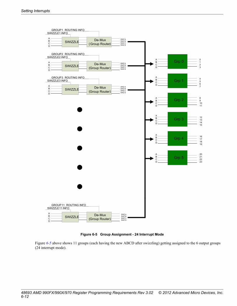
Setting Interrupts
Figure 6-5 Group Assignment - 24 Interrupt Mode
Figure 6-5 above shows 11 groups (each having the new ABCD after swizzling) getting assigned to the 6 output groups (24 interrupt mode).
Grp 0
Grp 1
Grp 2
Grp 3
Grp 4
Grp 5
ABCD
ABCD
ABCD
ABCD
ABCD
ABCD
0123
4567
891011
12131415
16171819
20212223
SWIZZLE
SWIZZLE 1 INFO
De-Mux(Group Router)
GROUP 1 ROUTING INFO
ABCD
SWIZZLE
SWIZZLE 11 INFO
De-Mux(Group Router)
GROUP 11 ROUTING INFO
ABCD
SWIZZLE
SWIZZLE 2 INFO
De-Mux(Group Router)
GROUP 2 ROUTING INFO
ABCD
SWIZZLE
SWIZZLE 3 INFO
De-Mux(Group Router)
GROUP 3 ROUTING INFO
ABCD
SWZ ASWZ BSWZ CSWZ D
SWZ ASWZ BSWZ CSWZ D
SWZ ASWZ BSWZ CSWZ D
SWZ ASWZ BSWZ CSWZ D
48693 AMD 990FX/990X/970 Register Programming Requirements Rev 3.02 © 2012 Advanced Micro Devices, Inc.6-12

Setting Interrupts
6.3.5 IOAPIC Interrupt Interrupt Status Register
Table 6-14 IOAPIC Interrupt interrupt Status Register
ASIC Rev Register
Address in IOAPIC
configuration space
Field Name Bits Description
RD9xx All Revs
IOAPIC_serial_IRQ_Status 0x0A Internal_irq_sts 31:0 Read Only. This is for debugging purpose only. This register shows each of the 32 interrupt status going into the IOAPIC. Note that the polarity of certain bits are reversed.
© 2012 Advanced Micro Devices, Inc. 48693 AMD 990FX/990X/970 Register Programming Requirements Rev 3.026-13

Southbridge Re-Routing Feature
6.4 Southbridge Re-Routing Feature
Once the 58 interrupts are mapped to either 32 or 24 interrupts, the IOAPIC decides which of the 32 or 24 interrupts are supposed to be active. The CPU indicates this by setting the MASK bit of the corresponding interrupt in the interrupt table entry. (This will be explained later, once the Memory mapped space is explained. For now it is correct to assume that each of the 32/24 interrupts has a corresponding MASK bit assigned, which decides whether the interrupt is active or disabled.) The southbridge feature allows the routing of the masked interrupt lines to the southbridge (see bit 4 in Table 6-5).
Figure 6-6 Routing of the Masked Interrupt Lines to the Southbridge
The mapping of the 32/24 masked interrupts to the 8-bit vector (A, B, C, D, E, F, G, H) is as follows:
If Mode is set to 1 (32 interrupts):A = Int0 OR Int8 OR Int16 OR Int24
B = Int1 OR Int9 OR Int17 OR Int25
C = Int2 OR Int10 OR Int18 OR Int26
D = Int3 OR Int11 OR Int19 OR Int27
E = Int4 OR Int12 OR Int20 OR Int28
F = Int5 OR Int13 OR Int21 OR Int29
G = Int6 OR Int14 OR Int22 OR Int30
H = Int7 OR Int15 OR Int23 OR Int31
If Mode is set to 0 (24 Interrupts):A = Int0 OR Int8 OR Int16
B = Int1 OR Int9 OR Int17
C = Int2 OR Int10 OR Int18
D = Int3 OR Int11 OR Int19
E = Int4 OR Int12 OR Int20
F = Int5 OR Int13 OR Int21
Masked Interrupts router
A B C D E F G H(To South Bridge )
32 or 24 mapped interrupts
Corresponding Mask bits
South bridge feature Enable
48693 AMD 990FX/990X/970 Register Programming Requirements Rev 3.02 © 2012 Advanced Micro Devices, Inc.6-14

Redirection Table Entry Registers
G = Int6 OR Int14 OR Int22
H = Int7 OR Int15 OR Int23
In general the IOAPIC does not send any interrupt message if the interrupt is masked. If the southbridge feature is set, then the masked interrupt will be routed to the southbridge. If the southbridge feature is not set, no interrupts will be sent to the southbridge and the masked interrupt will be treated as masked.
6.4.1 Recommended Usage
The IOAPIC should be enabled by the system BIOS and the southbridge routing feature should be switched on. This will allow the interrupts to be forwarded to the PIC in the southbridge. This way, if the system boots in DOS, interrupts will still work. Once the system boots an ACPI OS (where IOAPIC is assumed to be supported), the system BIOS will disable the southbridge routing feature so that the masked interrupts are masked out.
6.5 Redirection Table Entry Registers
These are 64-bit registers. Each of the mapped interrupt has a redirection table entry assigned to it. A redirection table entry defines the features of the interrupt. In particular it defines:
• Interrupt Vector – The vector associated with that interrupt pin. The CPU uses this vector to find out who sent the interrupt. Also for the EOI, the CPU writes/broadcasts this vector number to clear the interrupt
• Delivery Mode – The priority of the interrupt.
• Destination Mode – Whether the interrupt is going to a logical address or a physical address.
• Delivery Status – Whether the IOAPIC has sent the interrupt message corresponding to this pin or it is still pending.
• Interrupt Pin Polarity – Active high or active low. Note that the IOAPIC does not support active low interrupts, therefore this bit should always be set to 0.
• Remote IRR – This bit talks about the level sensitive interrupt and tells the CPU whether it has cleared this interrupt by sending an EOI or not. This bit will go high once the interrupt message corresponding to that pin has been sent.
• Trigger Mode – Whether the interrupt is level sensitive or edge sensitive.
• Mask – Whether the interrupt pin has been disabled or not. All interrupts are masked by default (bit set to 1). The CPU needs to write a 0 to unmask.
• Destination Address – Destination address of the interrupt message.
© 2012 Advanced Micro Devices, Inc. 48693 AMD 990FX/990X/970 Register Programming Requirements Rev 3.026-15
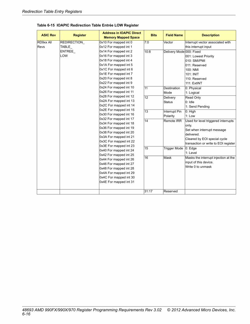
Redirection Table Entry Registers
Table 6-15 IOAPIC Redirection Table Entrée LOW Register
ASIC Rev RegisterAddress in IOAPIC Direct Memory Mapped Space
Bits Field Name Description
RD9xx All Revs
REDIRECTION_TABLE_ENTREE_LOW
0x10 For mapped int 00x12 For mapped int 10x14 For mapped int 20x16 For mapped int 30x18 For mapped int 40x1A For mapped int 50x1C For mapped int 60x1E For mapped int 70x20 For mapped int 80x22 For mapped int 90x24 For mapped int 100x26 For mapped int 110x28 For mapped int 120x2A For mapped int 130x2C For mapped int 140x2E For mapped int 150x30 For mapped int 160x32 For mapped int 170x34 For mapped int 180x36 For mapped int 190x38 For mapped int 200x3A For mapped int 210x3C For mapped int 220x3E For mapped int 230x40 For mapped int 240x42 For mapped int 250x44 For mapped int 260x46 For mapped int 270x48 For mapped int 280x4A For mapped int 290x4C For mapped int 300x4E For mapped int 31
7:0 Vector Interrupt vector associated with this interrupt input
10:8 Delivery Mode 000: Fixed001: Lowest Priority010: SMI/PMI011: Reserved100: NMI101: INIT110: Reserved111: ExtINT
11 Destination Mode
0: Physical1: Logical
12 Delivery Status
Read Only0: Idle1: Send Pending
13 Interrupt Pin Polarity
0: High1: Low
14 Remote IRR Used for level triggered interrupts only.Set when interrupt message delivered.Cleared by EOI special cycle transaction or write to EOI register
15 Trigger Mode 0: Edge1: Level
16 Mask Masks the interrupt injection at the input of this device.Write 0 to unmask
31:17 Reserved
48693 AMD 990FX/990X/970 Register Programming Requirements Rev 3.02 © 2012 Advanced Micro Devices, Inc.6-16
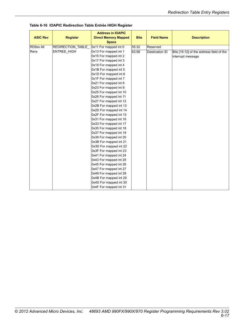
Redirection Table Entry Registers
Table 6-16 IOAPIC Redirection Table Entrée HIGH Register
ASIC Rev RegisterAddress in IOAPIC
Direct Memory Mapped Space
Bits Field Name Description
RD9xx All Revs
REDIRECTION_TABLE_ENTREE_HIGH
0x11 For mapped int 00x13 For mapped int 10x15 For mapped int 20x17 For mapped int 30x19 For mapped int 40x1B For mapped int 50x1D For mapped int 60x1F For mapped int 70x21 For mapped int 80x23 For mapped int 90x25 For mapped int 100x26 For mapped int 110x27 For mapped int 120x2B For mapped int 130x2D For mapped int 140x2F For mapped int 150x31 For mapped int 160x33 For mapped int 170x35 For mapped int 180x37 For mapped int 190x39 For mapped int 200x3B For mapped int 210x3D For mapped int 220x3F For mapped int 230x41 For mapped int 240x43 For mapped int 250x45 For mapped int 260x47 For mapped int 270x49 For mapped int 280x4B For mapped int 290x4D For mapped int 300x4F For mapped int 31
55:32 Reserved
63:56 Destination ID Bits [19:12] of the address field of the interrupt message
© 2012 Advanced Micro Devices, Inc. 48693 AMD 990FX/990X/970 Register Programming Requirements Rev 3.026-17

Redirection Table Entry Registers
This page intentionally left blank.
48693 AMD 990FX/990X/970 Register Programming Requirements Rev 3.02 © 2012 Advanced Micro Devices, Inc.6-18

Chapter 7RAS Settings
7.1 Overview
RAS features are not supported in RD9xx chipsets and will not function correctly. The following registers need to be programmed by System BIOS to hide partially visible RAS functions.
Table 7-1 Hiding RAS Functionality
ASIC Rev Register Setting Description
RD9xx All Revs
NBCONFIG x68 [14:12] = 0x0NBCONFIG x4 [10] = 0x1NBMISC x0 [0] = 0x1
Hide HT interrupt capabilities
© 2012 Advanced Micro Devices, Inc. 48693 AMD 990FX/990X/970 Register Programming Requirements Rev 3.027-1

Overview
This page intentionally left blank.
48693 AMD 990FX/990X/970 Register Programming Requirements Rev 3.02 © 2012 Advanced Micro Devices, Inc.7-2

Chapter 8IOMMU Initialization
This chapter describes initialization and feature programming of the RD9xx IOMMU subsystem.
8.1 IOMMU Configuration Space
The IOMMU configuration space consists of the following four groups:
• PCI Configuration space
• IOMMU Memory Mapped Register space
• IOMMU L1 Indexed space
• IOMMU L2 Indexed space
8.1.1 PCI Configuration Space
The PCI Configuration space consists of an IOMMU function (System Base Peripheral class and IOMMU sub-class) combined with an IOMMU capability. There are also MSI and MSI-Mapping capabilities in the capability chain. Multiple IOMMU functions may be located within a single system at Bus 0, Device 0, Function 2, where 0 is the primary bus number of the corresponding northbridge.
8.1.2 IOMMU Memory Mapped Register Space
The IOMMU Memory Mapped registers are mapped using the IOMMU Base Address Low register (Capability Offset 0x04) and IOMMU Base Address High register (Capability Offset 0x08) from IOMMU Capability Header, which starts at 0x40, specified in the PCI Configuration space.
8.1.3 IOMMU L1 Indexed Space
The IOMMU L1 Indexed space contains control and status registers that are generic to all L1s present in the IOMMU.
This register space is accessed through an index/data register pair located in the PCI Configuration space:
nbconfigfunc2:0xF8/0xFC (PCI Configuration Space, Bus 0, Device 0, Function 2)
The IOMMU L1 Indexed Space is subdivided into six parts as IOMMU has six L1s. Hardware has been implemented to provide a mechanism to access these registers independently, through the programming of bits [19:16] of the index register 0xF8. The encoding is as follows:
Table 8-1 IOMMU L1 Indexed Register
ASIC RevBus 0, Device 0, Function 2 : (IOMMU_L1, IOMMU_L2) :
L1CFG_INDEX · nbconfigfunc2:0xf8Function/Comment
RD9xx All Revs
NBCONFIGFUNC2:L1CFG_INDEX[15:0] = Register Offset · nbconfigfunc2:0xf8L1CFG_INDEX
Register Offset
NBCONFIGFUNC2:L1CFG_INDEX[19:16] = L1 Offset · nbconfigfunc2:0xf8L1CFG_SEL
Use the following encoding:0x0 for GFX0x1 for GFX20x2 for SB0x3 for GPP0x4 for GPP20x5 for VC1
NBCONFIGFUNC2:L1CFG_INDEX[31]=1’b1 · nbconfigfunc2:0xf8L1CFG_EN
Enable writing to L1CFG_DATA
© 2012 Advanced Micro Devices, Inc. 48693 AMD 990FX/990X/970 Register Programming Requirements Rev 3.028-1

IOMMU Initialization
8.1.4 IOMMU L2 Indexed Space
The IOMMU L2 Indexed Space contains control and status registers for IOMMU L2.
This register space is accessed through an index/data register pair located in the PCI Configuration Space. Please note the following for the index/data register pair:
nbconfigfunc2:0xF0/0xF4 (PCI Configuration Space, Bus 0, Device 0, Function 2)
8.2 IOMMU Initialization
NOTE: Steps described in this section need to be done for each IOMMU present in the system. Each IOMMU should use a different MMIO region for memory-mapped registers.
Table 8-2 IOMMU L1 Data Register
ASIC RevBus 0, Device 0, Function2 : (IOMMU_L1, IOMMU_L2):L1CFG_DATA·
nbconfigfunc2:0xfc Function/Comment
RD9xx All Revs
NBCONFIGFUNC2:L1CFG_DATA[31:0] = Register Offset · nbconfigfunc2:0xf8L1CFG_DATA
Data Value
Table 8-3 IOMMU L2 Indexed Register
ASIC RevBus 0, Device 0, Function2 : (IOMMU_L1, IOMMU_L2):L2CFG_INDEX ·
nbconfigfunc2:0xf0Function/Comment
RD9xx
All Revs
NBCONFIGFUNC2:L2CFG_INDEX[15:0]=Register Offset · nbconfigfunc2:0xf0
L2CFG_INDEX
Register Offset
NBCONFIGFUNC2:L2CFG_INDEX[8]=0x1 · nbconfigfunc2:0xf0
L2CFG_EN
Enable writing to L1CFG_DATA
Table 8-4 IOMMU L2 Data Register
ASIC RevBus 0, Device 0, Function2 : (IOMMU_L1, IOMMU_L2):L2CFG_DATA·
nbconfigfunc2:0xf4 Function/Comment
RD9xx All Revs
NBCONFIGFUNC2:L2CFG_DATA[31:0]=Register Offset · nbconfigfunc2:0xF4L2CFG_DATA
Data Value
Table 8-5 IOMMU Initialization
ASIC Rev Step Register Settings Function/Comment
RD9xx All Revs
1 NBCFG:IOC_FEATURE_CNTL[0]=0x1· NBMISCIND:0x75 IOC_FEATURE_CNTL_10_0Set bit [0] to 0x1.
Enable Access to Device 0, Function 2.
2 IOMMU_L2:IOMMU_CAP_BASE_LO[31:14] · nbconfigfunc2:0x44 IOMMU_BASE_ADDR_LOIOMMU_L2:IOMMU_CAP_BASE_HI[31:0] · nbconfigfunc2:0x48IOMMU_BASE_ADDR_HI
SBIOS must allocate a 16K region of MMIO space (16K aligned) for IOMMU memory-mapped registers. This base address of this region must be programmed into the IOMMU base address register.
RD9xx Rev A11 only
3 IOMMU_L2: IOMMU_CONTROL_W[8] =0x0nbconfigfunc2:0x6CIO_TLBSUP_WClear bit [8] to 0x0
For A11 only. Disable ATS support due to byte reverse ordering issue.
48693 AMD 990FX/990X/970 Register Programming Requirements Rev 3.02 © 2012 Advanced Micro Devices, Inc.8-2

IOMMU Initialization
8.2.1 IOMMU L1 Initialization
8.2.1.1 Enabling Phantom Function Support
To enable Phantom Function support, SBIOS is required to apply the algorithm described in Table 8-7 below.
RD9xx All Revs
4 IOMMU_L2:IOMMU_CAP_MISC[22]=0x0 · nbconfigfunc2:0x50 IOMMU_HT_ATS_RESVClear bit [22] to 0x0
SBIOS should ensure the Address Translation address range can be translated by the IOMMU.
5 IOMMU_L2:IOMMU_CAP_BASE_LO[0]=0x1· nbconfigfunc2:0x44 IOMMU_ENABLESet bit [0] to 0x1.
All IOMMU RW capability registers in PCI Configuration space are locked until the next system reset.
6 IOMMU_L2MMIO: IOMMU_MMIO_CMD_BASE_0 = 0x0Clear to 0x0
IOMMU_L2MMIO:IOMMU_MMIO_CMD_BASE_1 = 0x0800_0000Set to 0x0800_0000
IOMMU_L2MMIO:IOMMU_MMIO_EVENT_BASE_0 = 0x0Clear to 0x0
IOMMU_L2MMIO:IOMMU_MMIO_EVENT_BASE_1 = 0x0Clear to 0x0
IOMMU_L2MMIO:IOMMU_MMIO_CMD_BUF_TAILPTR_0 = 0x0Clear to 0x0
IOMMU_L2MMIO:IOMMU_MMIO_EVENT_BUF_HDPTR_0 = 0x0Clear to 0x0
Reset iommu mmio registers on warm reset, since they are only reset by a cold reset in hardware.
Table 8-6 IOMMU L1 Initialization
ASIC Rev Step Register Settings Function/Comment
RD9xx All Revs
1 IOMMU_L1:L1_CNTRL_0[30:28] = 0x7· L1CFGIND:0xCL1VirtOrderQueuesSet bits [30:28]=0x7
For each L1 increase virtual queues to maximum number for Virtual Queue hashing.
2 IOMMU_L1:L1_DEBUG_1[5]=0x1· L1CFGIND:0x7
Set bit [5]=0x1.
Enable ECO to prevent waiting for read completions on invalidations, this is a performance feature
Table 8-7 Enabling Phantom Function Support
ASIC Rev Step Field Settings Function/CommentRD9xx
All Revs1 In the PCIe® Configuration space of each PCIe device present
in the system, read back bits [4:3] of:PCIE_DEVICE_CAP[4:3] · (Offset 0x04 from PCI Express Capability ID)PHANTOM_FUNC
SBIOS will look into PCIe Configuration space of each PCIe device present in the system after the enumeration and read back whether any device residing on all ports of each multi-port PCIe core advertises support for Phantom Function.
Table 8-5 IOMMU Initialization (Continued)
ASIC Rev Step Register Settings Function/Comment
© 2012 Advanced Micro Devices, Inc. 48693 AMD 990FX/990X/970 Register Programming Requirements Rev 3.028-3
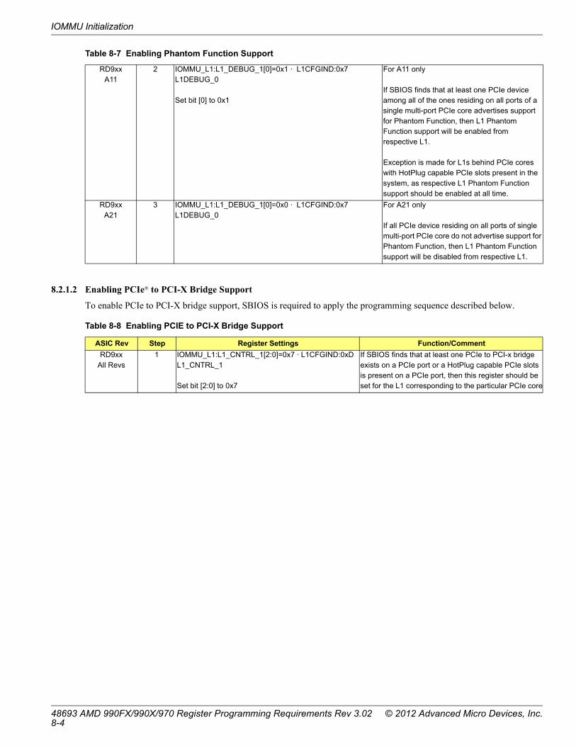
IOMMU Initialization
8.2.1.2 Enabling PCIe® to PCI-X Bridge Support
To enable PCIe to PCI-X bridge support, SBIOS is required to apply the programming sequence described below.
RD9xx A11
2 IOMMU_L1:L1_DEBUG_1[0]=0x1 · L1CFGIND:0x7 L1DEBUG_0
Set bit [0] to 0x1
For A11 only
If SBIOS finds that at least one PCIe device among all of the ones residing on all ports of a single multi-port PCIe core advertises support for Phantom Function, then L1 Phantom Function support will be enabled from respective L1.
Exception is made for L1s behind PCIe cores with HotPlug capable PCIe slots present in the system, as respective L1 Phantom Function support should be enabled at all time.
RD9xx A21
3 IOMMU_L1:L1_DEBUG_1[0]=0x0 · L1CFGIND:0x7 L1DEBUG_0
For A21 only
If all PCIe device residing on all ports of single multi-port PCIe core do not advertise support for Phantom Function, then L1 Phantom Function support will be disabled from respective L1.
Table 8-8 Enabling PCIE to PCI-X Bridge Support
ASIC Rev Step Register Settings Function/Comment
RD9xx All Revs
1 IOMMU_L1:L1_CNTRL_1[2:0]=0x7 · L1CFGIND:0xD L1_CNTRL_1
Set bit [2:0] to 0x7
If SBIOS finds that at least one PCIe to PCI-x bridge exists on a PCIe port or a HotPlug capable PCIe slots is present on a PCIe port, then this register should be set for the L1 corresponding to the particular PCIe core
Table 8-7 Enabling Phantom Function Support
48693 AMD 990FX/990X/970 Register Programming Requirements Rev 3.02 © 2012 Advanced Micro Devices, Inc.8-4

IOMMU Initialization
8.2.2 IOMMU L2 Initialization
8.2.2.1 IOMMU L2 Common Initialization
Table 8-9 IOMMU L2 Initialization
ASIC Rev Step Register Settings Function/CommentRD9xx
All Revs1 IOMMU_L2AINDX:L2_CONTROL_0[29]=0x1 · L2CFGIND:0xC
IFifoClientPrioritySet bit [29] to 0x1
Set attribute to VC1 L1 client to be arbitrated as high priority.
2 IOMMU_L2AINDX:L2_DTC_CONTROL[9:8]=0x2 ·L2CFGIND:0x10DTCInvalidationSelSet bits [9:8] to 0x2
Select DTC cache Invalidation Algorithm to be sequential precise invalidation.
3 IOMMU_L2AINDX:L2_ITC_CONTROL[9:8] =0x2 · L2CFGIND:0x14ITCInvalidationSelSet bits [9:8] to 0x2
Select ITC cache Invalidation Algorithm to be sequential precise invalidation.
4 IOMMU_L2AINDX:L2_PTC_A_CONTROL[9:8] =0x2 ·L2CFGIND:0x18PTCAInvalidationSelSet bits [9:8] to 0x2
Select PTC Cache A Invalidation Algorithm to be sequential precise invalidation.
5 IOMMU_L2AINDX:L2_PTC_B_CONTROL[9:8] =0x2 ·L2CFGIND:0x1CPTCBInvalidationSelSet bits [9:8] to 0x2
Select PTC Cache B Invalidation Algorithm to be sequential precise invalidation.
6 IOMMU_L2INDX:L2_PDC_CONTROL [9:8]=0x2 · L2CFGIND:0x50PDCInvalidationSelSet bits [9:8] to 0x2
Select PDC Cache Invalidation Algorithm to be sequential precise invalidation.
RD9xx All Revs
7 IOMMU_L2AINDX:L2_DTC_CONTROL[4]=0x1·L2CFGIND:0x10DTCParityEnSet bit [4] to 0x1.
Enable parity protection of DTC Cache.
8 IOMMU_L2AINDX:L2_ITC_CONTROL[4]=0x1 · L2CFGIND:0x14 ITCParityEnSet bit [4] to 0x1.
Enable parity protection of ITC Cache.
9 IOMMU_L2AINDX:L2_PTC_A_CONTROL[4]=0x1 · L2CFGIND:0x18PTCAParityEnSet bit [4] to 0x1.
Enable parity protection of PTC Cache A.
10 IOMMU_L2AINDX:L2_PTC_B_CONTROL[4]=0x1 ·L2CFGIND:0x1CPTCBParityEnSet bit [4] to 0x1.
Enable parity protection of PTC Cache B.
11 IOMMU_L2INDX:L2_PDC_CONTROL[4]=0x1· L2CFGIND:0x50 PDCParityEnSet bit [4] to 0x1.
Enable parity protection of PDC Cache.
RD9xxA21
12 IOMMU_L2AINDX:L2_DEBUG_0[7]=0x1· L2CFGIND:0x6
L2DEBUG0Set bit [7] to 0x1.
IOMMU_L2INDX:L2_DEBUG_3[0]=0x1· L2CFGIND:0x47
L2DEBUG3Set bit [0] to 0x1.
Page mode does not override IoCtl and
SysMgt DTE attributes.
© 2012 Advanced Micro Devices, Inc. 48693 AMD 990FX/990X/970 Register Programming Requirements Rev 3.028-5

IOMMU Initialization
RD9xxA21
13 IOMMU_L2AINDX:L2_DEBUG_1[1]=0x1· L2CFGIND:0x7
L2DEBUG1Set bit [1] to 0x1.
IOMMU_L2INDX:L2_DEBUG_3[1]=0x1· L2CFGIND:0x47 L2DEBUG3Set bit [1] to 0x1.
Avoid aborting untranslated memory requests
or address translation requests when any of
the following --exclusion range address,
system management range address, or I/O
space range address -- is configured to block
or pass through requests, and is located
above the largest virtual address defined in
the device table page mode field.
Avoid aborting untranslated memory requests
to the exclusion range, when the system
management range address and/or the I/O
space range address are configured to block
or pass through requests, and when the
device table entry has the translation valid bit
cleared.
14 IOMMU_L2AINDX:L2_DEBUG_1[2]=0x1· L2CFGIND:0x7 L2DEBUG1
Set bit [2] to 0x1.
Abort address translation request in the system management address range when device table entry has SysMgt=0x0, 0x1 or 0x2 and IntTaLen[3:2]=0x3 or when device table entry has SysMgt=0x3, IntTaLen[3:2]= 0x3, V=0x1 and TV=0x0.
15 IOMMU_L2AINDX:L2_DEBUG_1[3]=0x1· L2CFGIND:0x7 L2DEBUG1Set bit [3] to 0x1.
IOMMU_L2INDX:L2_DEBUG_3[3]=0x1· L2CFGIND:0x47 L2DEBUG3Set bit [3] to 0x1.
Avoid treating interrupt requests as
untranslated memory requests or address
translation requests from exclusion range
under specific conditions.
16 IOMMU_L2AINDX:L2_DEBUG_1[4]=0x1· L2CFGIND:0x7 L2DEBUG1
Set bit [4] to 0x1.
Abort DMA read request in the HT interrupt
address range when device table entry has IV
bit cleared.
17 IOMMU_L2AINDX:L2_DEBUG_0[5]=0x1· L2CFGIND:0x6 L2DEBUG0
Set bit [5] to 0x1.
Avoid corruption of EX bit when IOMMU has
cached device table entry.
18 IOMMU_L2AINDX:L2_DEBUG_0[6]=0x1· L2CFGIND:0x6 L2DEBUG0
Set bit [6] to 0x1.
Avoid corruption of SE bit when IOMMU has
cached device table entry.
19 IOMMU_L2AINDX:L2_DEBUG_1[5]=0x1· L2CFGIND:0x7 L2DEBUG1Set bit [5] to 0x1.
IOMMU_L2INDX:L2_DEBUG_3[4]=0x1· L2CFGIND:0x47 L2DEBUG3Set bit [4] to 0x1.
Avoid access right checks for pretranslated
requests.
20 IOMMU_L2AINDX:L2_DEBUG_1[6]=0x1· L2CFGIND:0x7 L2DEBUG1
Set bit [6] to 0x1.
Avoid corruption of IG bit for Startup and EOI
interrupts.
21 IOMMU_L2AINDX:L2_DEBUG_1[7]=0x1· L2CFGIND:0x7 L2DEBUG1
Set bit [7] to 0x1.
Detect address translation request in the
interrupt address range in all conditions.
Table 8-9 IOMMU L2 Initialization (Continued)
ASIC Rev Step Register Settings Function/Comment
48693 AMD 990FX/990X/970 Register Programming Requirements Rev 3.02 © 2012 Advanced Micro Devices, Inc.8-6

IOMMU Initialization
RD9xxA21
22 IOMMU_L2AINDX:L2_DEBUG_0[8]=0x1· L2CFGIND:0x6 L2DEBUG0
Set bit [8] to 0x1.
Abort address translation request to exclusion
range when device table entry has both EX and
TV bits cleared.
23 IOMMU_L2INDX:L2_PDC_WAY_CONTROL[31:0]=0xF000 0002 · L2CFGIND:0x52PDCWayDisablePDCWayAccessDisable
Set bits [31:0] to 0xF000 0002.
Configure PDC cache to 12-way set
associative cache.
RD9xx
All Revs
24 IOMMU_L2INDX:L2_ERR_RULE_CONTROL_0[0]=0x1·
L2CFGIND:0x80
ERRRuleLock0
Set bit [0] to 0x1.
IOMMU_L2INDX:L2_ERR_RULE_CONTROL_3[0]=0x1·
L2CFGIND:0x30
ERRRuleLock1
Set bit [0] to 0x1.
Lock fault detection rule sets.
Table 8-9 IOMMU L2 Initialization (Continued)
ASIC Rev Step Register Settings Function/Comment
© 2012 Advanced Micro Devices, Inc. 48693 AMD 990FX/990X/970 Register Programming Requirements Rev 3.028-7

IOMMU Initialization
8.2.2.2 Optimizing IOMMU L2 Caches Performance Based on the Number of Functions/Devices/Buses in Use
For optimum performance of IOMMU L2 caches, SBIOS is required to scan all ReqIDs present in the configuration space topology of the system after enumeration and then apply the programming sequence described in Table 8-10 below.
The following relationship must be maintained for each IOMMU L2 cache:
BusBits + DeviceBits + FunctionBits = log2(CacheDepth/CacheAssociativity)
NOTE: All low performing devices behind the southbridge might be excluded from the algorithm for optimal cache indexing.
Table 8-10 Programming Sequence of L2 Caches Hash Control
ASIC Rev Step Field Settings Function/Comment
RD9xx All Revs
1 For each IOMMU L2 caches, calculate maximum number of FuncBits+ DevBits + BusBits which can be used in the algorithm, based on log2(CacheDepth/CacheAssociativity).
For DTC cache: Read back DTC cache depth by reading bits [31:28] of:
IOMMU_L2AINDX:L2_DTC_CONTROL[31:28]· L2CFGIND:0x10 DTCEntriesand DTC cache associativity by reading back bits [23:16] of:
IOMMU_L2AINDX:L2_DTC_CONTROL[23:16]· L2CFGIND:0x10 DTCWaysAs DTC cache depth = 2^ DTCEntries, calculate the maximum number of DTCFuncBits+ DTCDevBits + DTCBusBits bits which can be used in the algorithm based on:
DTCFuncBits + DTCDevBits + DTCBusBits = DTCEntries - log2(DTCWays)
For ITC cache:Read back ITC cache depth by reading bits [31:28] of:
IOMMU_L2AINDX:L2_ITC_CONTROL[31:28]· L2CFGIND:0x14 ITCEntriesand ITC cache associativity by reading back bits [23:16] of:
IOMMU_L2AINDX:L2_ITC_CONTROL[23:16]· L2CFGIND:0x14 ITCWaysAs ITC cache depth = 2^ ITCEntries, calculate the maximum number of ITCFuncBits+ ITCDevBits + ITCBusBits bits which can be used in the algorithm based on:
ITCFuncBits + ITCDevBits + ITCBusBits = ITCEntries - log2(ITCWays)
Step 1 to be continued on the next page
Determine maximum number of (function + bus + device) bits which can be used in the algorithm for each IOMMU L2 cache.
48693 AMD 990FX/990X/970 Register Programming Requirements Rev 3.02 © 2012 Advanced Micro Devices, Inc.8-8

IOMMU Initialization
RD9xx All Revs
1 Step 1 continued from the previous page
For PTCA cache:Read back PTCA cache depth by reading bits [31:28] of:
IOMMU_L2AINDX:L2_PTC_A_CONTROL[31:28]· L2CFGIND:0x18 PTCAEntriesand PTCA cache associativity by reading back bits [23:16] of:
IOMMU_L2AINDX:L2_PTC_A_CONTROL[23:16]· L2CFGIND:0x18 PTCAWaysAs PTCA cache depth = 2^ PTCAEntries, calculate the maximum number of PTCAFuncBits+ PTCADevBits + PTCABusBits bits which can be used in the algorithm based on:
PTCAFuncBits + PTCADevBits + PTCABusBits = PTCAEntries - log2(PTCAWays)
For PTCB cache:Read back PTCB cache depth by reading bits [31:28] of:
IOMMU_L2AINDX:L2_PTC_B_CONTROL[31:28]· L2CFGIND:0x1C PTCBEntriesand PTCB cache associativity by reading back bits [23:16] of:
IOMMU_L2AINDX:L2_PTC_B_CONTROL[23:16]· L2CFGIND:0x1C PTCBWays
As PTCB cache depth = 2^ PTCBEntries, calculate the maximum number of PTCBFuncBits+ PTCBDevBits + PTCBBusBits bits which can be used in the algorithm based on:
PTCBFuncBits + PTCBDevBits + PTCBBusBits = PTCBEntries - log2(PTCBWays)
For PDC cache:Read back PDC cache depth by reading bits [31:28] of:
IOMMU_L2INDX:L2_PDC_CONTROL[31:28] · L2CFGIND:0x50 PDCEntriesand PDC cache associativity by reading back bits [23:16] of:
IOMMU_L2INDX:L2_PDC_CONTROL[23:16] · L2CFGIND:0x50 PDCWaysAs PDC cache depth = 2^ PDCEntries, calculate the maximum number of PDCFuncBits+ PDCDevBits + PDCBBusBits bits which can be used in the algorithm based on:
PDCFuncBits + PDCDevBits + PDCBusBits = PDCEntries - log2(PDCWays)
Table 8-10 Programming Sequence of L2 Caches Hash Control (Continued)
ASIC Rev Step Field Settings Function/Comment
© 2012 Advanced Micro Devices, Inc. 48693 AMD 990FX/990X/970 Register Programming Requirements Rev 3.028-9

IOMMU Initialization
RD9xx All Revs
2 Identify the maximum function number present in the configuration space topology of the system and find FuncBits = log2(maxFunc +1).
For Single Root IOV devices, SBIOS is required to read back Total Number of Virtual Functions supported that are associated with each Physical Function. To identify TotalVFs supported by the device, follow the extended capability linked list in the device’s PCI Express configuration space, to find the SR-IOV Extended Capability header (capability ID = 0x0010), and then read back bits [15:0] at offset 0xE from SR-IOV Extended Capability. TotalVFs read, should then be taken as max function number sub-set representative. If TotalVFs >0x40, then clamp the max function number of sub-set representative to 0x40.
For server systems, all southbridge internal device utilizing multiple functions might be bypassed for FuncBits calculation.
Identify maximum function number present in the system.
3 Identify the maximum device number present in the configuration space topology of the system and find DevBits = log2(maxDevice +1).
Identify maximum device number present in the system.
4 Identify the maximum bus number present in the configuration space topology of the system and find BusBits = log2(maxBus +1).
Identify maximum bus number present in the system.
5 For each IOMMU L2 cache, determine the actual number of function bits which will be used for optimal cache performance, referenced in the algorithm as FuncBitsUsed.FuncBitsUsed = 0x3.
Store FuncBitsUsed in respective fields for all L2 caches:IOMMU_L2AINDX:L2_DTC_HASH_CONTROL[1:0]= FuncBitsUsed · L2CFGIND:0x11 DTCFuncBitsIOMMU_L2AINDX:L2_ITC_HASH_CONTROL[1:0]= FuncBitsUsed · L2CFGIND:0x15 ITCFuncBitsIOMMU_L2AINDX:L2_PTC_A_HASH_CONTROL[1:0]= FuncBitsUsed · L2CFGIND:0x19 PTCAFuncBitsIOMMU_L2AINDX:L2_PTC_B_HASH_CONTROL[1:0]= FuncBitsUsed · L2CFGIND:0x1D PTCBFuncBitsIOMMU_L2INDX:L2_PDC_HASH_CONTROL[1:0] = FuncBitsUsed · L2CFGIND:0x51 PDCFuncBits
Determine the optimal number of function bits to be used for optimal IOMMU L2 caches performance.
Table 8-10 Programming Sequence of L2 Caches Hash Control (Continued)
ASIC Rev Step Field Settings Function/Comment
48693 AMD 990FX/990X/970 Register Programming Requirements Rev 3.02 © 2012 Advanced Micro Devices, Inc.8-10

IOMMU Initialization
RD9xx All Revs
6 For each IOMMU L2 cache, determine the actual number of device bits which will be used for optimal cache performance, referenced in the algorithm as DevBitsUsed.If max(DevBits,FuncBits-0x3) + 0x3 >= log2(CacheDepth/CacheAssociativity), then DevBitsUsed = log2(CacheDepth/CacheAssociativity) – max(DevBits , FuncBits -0x3) -0x3,store DevBitsUsed in respective fields for all L2 caches, and exit the algorithm.
If max(DevBits, FuncBits -0x3) +0x3 < log2(CacheDepth/CacheAssociativity), thenDevBitsUsed = max(DevBits , FuncBits - 0x3 ), store DevBitsUsed in respective fields and go to Step7.
Store DeviceBitsUsed determined in Step5 in respective fields for all L2 caches:IOMMU_L2AINDX:L2_DTC_HASH_CONTROL[4:2 ]= DeviceBitsUsed · L2CFGIND:0x11DTCDevBitsIOMMU_L2AINDX:L2_ITC_HASH_CONTROL[4:2] = DeviceBitsUsed · L2CFGIND:0x15ITCDevBitsIOMMU_L2AINDX:L2_PTC_A_HASH_CONTROL[4:2] = DeviceBitsUsed · L2CFGIND:0x19 PTCADevBitsIOMMU_L2AINDX:L2_PTC_B_HASH_CONTROL[4:2] = DeviceBitsUsed · L2CFGIND:0x1D PTCBDevBitsIOMMU_L2INDX:L2_PDC_HASH_CONTROL[4:2] = DeviceBitsUsed · L2CFGIND:0x51
PDCDevBits
Determine the optimal number of device bits to be used for optimal IOMMU L2 caches performance.
7 For each IOMMU L2 cache, determine the actual number of bus bits which will be used for optimal cache performance, referenced in the algorithm as BusBitsUsed.BusBitsUsed = log2(CacheDepth/CacheAssociativity) – DevBitsUsed – FuncBitsUsed,store BusBitsUsed in respective fields for all L2 caches, and exit the algorithm.
Store BusBitsUsed in respective fields for all L2 cachesIOMMU_L2AINDX:L2_DTC_HASH_CONTROL[8:5]= BusBitsUsed · L2CFGIND:0x11 DTCBusBitsIOMMU_L2AINDX:L2_ITC_HASH_CONTROL[8:5]= BusBitsUsed · L2CFGIND:0x15 ITCBusBitsIOMMU_L2AINDX:L2_PTC_A_HASH_CONTROL[8:5]= BusBitsUsed · L2CFGIND:0x19 PTCABusBitsIOMMU_L2AINDX:L2_PTC_B_HASH_CONTROL[8:5]= BusBitsUsed · L2CFGIND:0x1D PTCBBusBitsIOMMU_L2INDX:L2_PDC_HASH_CONTROL[8:5]= BusBitsUsed · L2CFGIND:0x51 PDCBusBits
Determine the optimal number of bus bits to be used for optimal IOMMU L2 caches performance.
Table 8-10 Programming Sequence of L2 Caches Hash Control (Continued)
ASIC Rev Step Field Settings Function/Comment
© 2012 Advanced Micro Devices, Inc. 48693 AMD 990FX/990X/970 Register Programming Requirements Rev 3.028-11

Virtualization ACPI Tables
8.3 Virtualization ACPI Tables
SBIOS is required to describe the IOMMUs present in the system along with their respective attributes as well as system I/O topology via configuration of I/O Virtualization ACPI tables. System software then honors the ACPI settings.
8.3.1 I/O Virtualization ACPI Tables Configuration
There are three types of data blocks defined by SBIOS in the IOMMU ACPI tables:
• I/O Virtualization Reporting Structure (IVRS)
• I/O Virtualization Hardware Definition (IVHD)
• I/O Virtualization Memory Definition (IVMD)
They are described in the sections below.
8.3.1.1 I/O Virtualization Reporting Structure (IVRS)
SBIOS is required to build a single I/O Virtualization Reporting Structure (IVRS) block in a system that contains IOMMU/s.
For IVRS Table definition and individual fields description, refer to IOMMU 1.22+ specification.
The programming sequence of IVRS fields is described in Table 8-11 below.
8.3.1.2 I/O Virtualization Hardware Definition Block (IVHD)
SBIOS is required to build a single I/O Virtualization Hardware Definition (IVHD) block for each IOMMU that is present in the system.
For IVHD Table definition and individual fields description, refer to IOMMU 1.22+ specification.
Table 8-11 Programming Sequence of IOMMU IVRS
ASIC Rev Step Field Settings Function/CommentRD9xx
All Revs1 Signature (“IVRS”) ASCII encoding of IVRS.
2 Length (bytes) SBIOS is required to calculate length of total device reporting structure in bytes, including IVHD and IVMD structures, and populate the field.
3 Revision = 0x1 IVRS revision number.
4 Check SBIOS is required to calculate the checksum of the entire device reporting structure, including IVHD and IVMD structures, and populate this field, so that the total checksum is zero.
5 OEM ID Identifies platform OEM.
6 OEM Table ID Specified by OEM.
7 OEM Revision Specified by OEM.
8 Creator ID Vendor ID of the utility that created the table
9 Creator Revision Revision of the utility that created the table
10 Ivinfo IVinfo field contains information common to all IOMMUs in a system.
IVinfo[31:23]=0x0Reserved.
Reserved.
IVinfo[22]=0x0HtAtsResv
ATS address translation range can be used for translation.
IVinfo[21:15]=0x40VAsize
Maximum supported Virtual address size is 64 bits.
IVinfo[14:8]=0x34PAsize
Maximum supported Physical address size is 52 bits.
IVinfo[7:0]=0x0Reserved.
Reserved.
48693 AMD 990FX/990X/970 Register Programming Requirements Rev 3.02 © 2012 Advanced Micro Devices, Inc.8-12

Virtualization ACPI Tables
The programming sequence of IOHD general fields is described in the table below below.
Table 8-12 Programming Sequence of IOMMU IVHD General Fields
ASIC Rev Step Field Settings Function/Comment
RD9xx All Revs
1 Type=0x10 I/O virtualization hardware definition block.
2 IVHD flags IVinfo field contains information common to all IOMMUs in a system.
IVHD flags [7:5]=0x0Reserved.
Reserved
IVHD flags[4] IotlbSup
If IoTlbSup = 0x1, OEMs may choose to enable ATS support by having SBIOS set this flag or disable ATS support by clearing this flag, regardless of the state of the IoTlbSup register in PCI configuration space.
IVHD flags[3]= 0x1Isoc
Indicate to system software the value that should be programmed into ISOC field of MMIO register at offset 0x18h.
IVHD flags[2]= 0x1ResPassPW
Indicate to system software the value that should be programmed into RES_PASS_PW field of MMIO register at offset 0x18.
IVHD flags[1]= 0x1 PassPW
Indicate to system software the value that should be programmed into PASS_PW field of MMIO register at offset 0x18.
IVHD flags[0]= 0x0 HtTunEnNOTE: Register setting for HtTunEn does not apply as RD9xx is a cave device.
Override MMIO Offset 0x0018[HtTunEn] for system software.
3 Length SBIOS is required to calculate the size of the entire IVHD, including IVHD device entries in bytes, starts from Type field and record the value in this entry.
4 Bus n, Device 0, Function 2 DeviceID of IOMMU.5 Capability offset Offset in Capability space for control fields of IOMMU. It is
required as IOMMU implements multiple capabilities.6 IOMMU base address SBIOS is required to populate this field with Base address of
IOMMU control registers once it maps them in Memory Mapped space.
7 PCI segment=0x0 PCI Segment numberRD9xx
All Revs8 IOMMU info MSI number and UnitID
IOMMU info[15:13]= 0x0Reserved.
Reserved
IOMMU info[12:8]=0x14Unit ID
Unit ID number (Capability Offset 0Ch[UnitID])
IOMMU info[7:5]=0x0Reserved.
Reserved.
IOMMU info[4:0]=0x0 MSI message number RD9xx
All Revs9 I/O Virtualization Hardware Definition
(IVHD) bytes at offset 0x44-0x47 are reserved and hence these fields should be cleared.
Reserved
© 2012 Advanced Micro Devices, Inc. 48693 AMD 990FX/990X/970 Register Programming Requirements Rev 3.028-13

Virtualization ACPI Tables
8.3.1.3 I/O Virtualization Definition Blocks (IVHD) Device Entries
The IVHD Table uses 4 and 8 bytes long entries to describe all devices present in the system.
Table 8-13 IVHD Devices Entries
ASIC Rev Step Field Settings Function/Comment
RD9xx All Revs
1 Use 4-byte entry of Type 0x2 in order to describe the Southbridge SMBUS Controller:
SB SBMUS Controller IVHD Entry.NOTE: If the system contains more than one IOMMU, SB SMBUS Controller needs to be described only for the IOMMU attached to the Southbridge.
Byte0=Select Byte1 & Byte2 Byte3=Data
Byte0[7:0]=0x2 Bus 0x0, Device 0x14, Function 0x0.
Byte3[7]=0x1Lint1Pass
Byte3[6]=0x0Lint0Pass
Byte3[5:4]=0x1SysMgt
Byte3[3]=0x0Reserved
Byte3[2]=0x1NMIPass
Byte3[1]=0x1EIntPass
Byte3[0]=0x1INITPass
2 Use 4-byte entry of Type 0x2 to describe all internal Southbridge devices other than SMBUS controller (e.g. USB controller, SATA controller etc.)
SB Devices other than SMBUS controller IVHD EntryNOTE: If the system contains more than one IOMMU, Southbridge devices need to be described only for the IOMMU attached to the Southbridge
Byte0=Select Byte1 & Byte2 Byte3=Data
Byte0[7:0]=0x2 Bus 0, Device, Function from PCI Configuration Topology for each SB device other than SMBUS controller
Byte3[7]=1’b0Lint1Pass
Byte3[6]=1’b0Lint0Pas s
Byte3[5:4]=1’b00SysMgt
Byte3[3]=1’b0Reserved
Byte3[2]=1’b0NMIPass
Byte3[1]=1’0EIntPass
Byte3[0]=1’b0INITPass
3 Use 4-byte entry of Type 0x2 to describe a single device behind the PCIe® bridgeor use Type 0x3 and 0x4 in order to describe a range of devices behind PCIe bridge.
Device/s behind PCIe bridge/s;
Byte0=Select Byte1 & Byte2 Byte3=Data
For a single device behind PCIe bridge:
Byte0[7:0]=0x2
For a range of devices behind PCIe bridges:
Byte0[7:0]=0x3Start of the range
Byte0[7:0]=0x4End of the range
DeviceID (Bus, Device, Function) from PCI Configuration Topology.
Byte3[7]=0x0Lint1Pass
Byte3[6]=0x0Lint0Pass
Byte3[5:4]=0x0SysMgt
Byte3[3]=0x0Reserved
Byte3[2]=0x0NMIPass
Byte3[1]=0x0EIntPass
Byte3[0]=0x0INITPass
48693 AMD 990FX/990X/970 Register Programming Requirements Rev 3.02 © 2012 Advanced Micro Devices, Inc.8-14

Virtualization ACPI Tables
RD9xx All Revs
4 Use 8-byte entry of Type 0x42 (Alias Select) to describe:1. Single device behind PCI bridge.2. Single device behind a PCI-X bridge operating in PCI mode.
Or use Type 0x43 (Alias Start of the Range) to describe:1. Range of devices behind PCI bridge.2. Range of devices behind a PCI-X bridge operating in PCI-X mode.
Device/s behind PCI bridge/s;Device/s behind a PCI-X bridge/s operating in PCI mode IVHD Entries.
Byte0=Select Byte1 & Byte2 Byte3=Data
For:1.Single device behind PCI bridge;2. Single device behind a PCI-X bridge operating in PCI mode:
Byte0[7:0]=0x42
For:1.Range of devices behind PCI bridge;2.Range of devices behind a PCI-X bridge operating in PCI mode:
Byte0[7:0]=0x43Start of the range
NOTE: Range is terminated with entry of Type 4:Byte0[7:0]=0x4End of the range
DeviceID (Bus, Device, Function) from PCI Configuration Topology.
Byte3[7]=0x0Lint1Pass
Byte3[6]=0x0Lint0Pass
Byte3[5:4]=0x0SysMgt
Byte3[3]=0x0Reserved
Byte3[2]=0x0NMIPass
Byte3[1]=0x0EIntPass
Byte3[0]=0x0INITPass
Byte4=Reserved Byte5 & Byte6 Byte7=Reserved
Byte4[7:0]=0x0 SourceID used by peripheral.For all PCI-X and PCI devices: Bus = bridge secondary bus number (i.e., PCI-X/PCI bus), Device=0x0, Function=0x0.
Byte7[7:0]=0x0
Table 8-13 IVHD Devices Entries (Continued)
ASIC Rev Step Field Settings Function/Comment
© 2012 Advanced Micro Devices, Inc. 48693 AMD 990FX/990X/970 Register Programming Requirements Rev 3.028-15

Virtualization ACPI Tables
RD9xx All Revs
5 Use 8-byte entry of Type 0x42 (Alias Select) to describe a single device behind SB
Secondary PCI Bus.
Or use Type 0x43 (Alias Start of the Range) to describe a range of devices behind
SB Secondary PCI Bus.
Device/s behind SB Secondary PCI bus.
Byte0=Select Byte1 & Byte2 Byte3=Data
For:
Single device behind SB
Secondary PCI Bus.
Byte0[7:0]=0x42
For:
Range of devices behind SB
Secondary PCI Bus.
Byte0[7:0]=0x43
Start of the range
NOTE: Range is terminated
with entry of Type 4:
Byte0[7:0]=0x4
End of the range
DeviceID (Bus, Device,
Function) from PCI
Configuration Topology.
Byte3[7]= 0x0
Lint1Pass
Byte3[6]= 0x0
Lint0Pass
Byte3[5:4]= 0x0
SysMgt
Byte3[3]= 0x0
Reserved
Byte3[2]= 0x0
NMIPass
Byte3[1]= 0x0
EIntPass
Byte3[0]= 0x0
INITPass
Byte4=Reserved Byte5 & Byte6 Byte7=Reserved
Byte4[7:0]=0x0 SourceID used by
peripheral.
Bus = 0x0, Device=0x14,
Function from PCI
Configuration Topology.
Byte7[7:0]= 0x0
Table 8-13 IVHD Devices Entries (Continued)
ASIC Rev Step Field Settings Function/Comment
48693 AMD 990FX/990X/970 Register Programming Requirements Rev 3.02 © 2012 Advanced Micro Devices, Inc.8-16

Virtualization ACPI Tables
RD9xx All Revs
6 Use 8-byte entry of type 0x48 in order to describe IOAPIC (one for NB and one for
SB) as a special device that cannot be identified through enumeration.
NB IOAPIC, SB IOAPIC IVHD Entry.
Byte0=Select Byte1 & Byte2 Byte3=Data
Byte0[7:0]=0x48 0x0 NB IOAPIC:
Byte3[7]=0x0
Lint1Pass
SB IOAPIC:
Byte3[7]=0x1
Lint1Pass
NB IOAPIC:
Byte3[6]=0x0
Lint0Pass
SB IOAPIC:
Byte3[6]=0x1
Lint0Pass
NB IOAPIC:
Byte3[5:4]= 0x0
SysMgt
SB IOAPIC:
Byte3[5:4]= 0x1
SysMgt
Byte3[3]= 0x0
Reserved
NB IOAPIC:
Byte3[2]= 0x0
NMIPass
SB IOAPIC:
Byte3[2]= 0x1
NMIPass
NB IOAPIC:
Byte3[1]= 0x0
EIntPass
SB IOAPIC:
Byte3[1]= 0x1
EIntPass
NB IOAPIC:
Byte3[0]= 0x0
INITPass
SB IOAPIC:
Byte3[0]= 0x1
INITPass
Table 8-13 IVHD Devices Entries (Continued)
ASIC Rev Step Field Settings Function/Comment
© 2012 Advanced Micro Devices, Inc. 48693 AMD 990FX/990X/970 Register Programming Requirements Rev 3.028-17
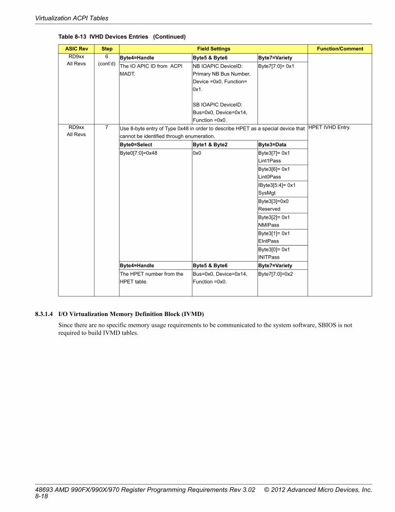
Virtualization ACPI Tables
8.3.1.4 I/O Virtualization Memory Definition Block (IVMD)
Since there are no specific memory usage requirements to be communicated to the system software, SBIOS is not required to build IVMD tables.
RD9xx All Revs
6(cont’d)
Byte4=Handle Byte5 & Byte6 Byte7=Variety
The IO APIC ID from ACPI
MADT.
NB IOAPIC DeviceID:
Primary NB Bus Number,
Device =0x0, Function=
0x1.
SB IOAPIC DeviceID:
Bus=0x0, Device=0x14,
Function =0x0.
Byte7[7:0]= 0x1
RD9xx All Revs
7 Use 8-byte entry of Type 0x48 in order to describe HPET as a special device that
cannot be identified through enumeration.
HPET IVHD Entry.
Byte0=Select Byte1 & Byte2 Byte3=Data
Byte0[7:0]=0x48 0x0 Byte3[7]= 0x1
Lint1Pass
Byte3[6]= 0x1
Lint0Pass
IByte3[5:4]= 0x1
SysMgt
Byte3[3]=0x0
Reserved
Byte3[2]= 0x1
NMIPass
Byte3[1]= 0x1
EIntPass
Byte3[0]= 0x1
INITPass
Byte4=Handle Byte5 & Byte6 Byte7=Variety
The HPET number from the
HPET table.
Bus=0x0, Device=0x14,
Function =0x0.
Byte7[7:0]=0x2
Table 8-13 IVHD Devices Entries (Continued)
ASIC Rev Step Field Settings Function/Comment
48693 AMD 990FX/990X/970 Register Programming Requirements Rev 3.02 © 2012 Advanced Micro Devices, Inc.8-18
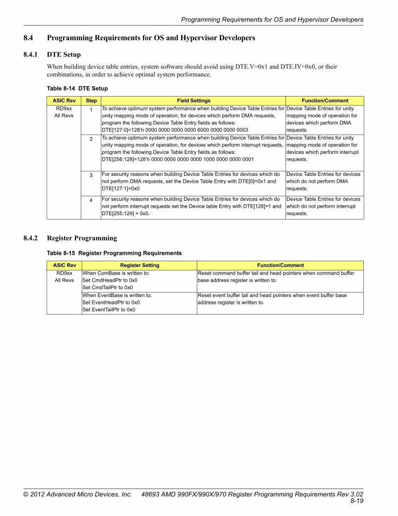
Programming Requirements for OS and Hypervisor Developers
8.4 Programming Requirements for OS and Hypervisor Developers
8.4.1 DTE Setup
When building device table entries, system software should avoid using DTE.V=0x1 and DTE.IV=0x0, or their combinations, in order to achieve optimal system performance.
8.4.2 Register Programming
Table 8-14 DTE Setup
ASIC Rev Step Field Settings Function/Comment
RD9xx All Revs
1 To achieve optimum system performance when building Device Table Entries for unity mapping mode of operation, for devices which perform DMA requests, program the following Device Table Entry fields as follows:DTE[127:0]=128’h 0000 0000 0000 0000 6000 0000 0000 0003
Device Table Entries for unity mapping mode of operation for devices which perform DMA requests.
2 To achieve optimum system performance when building Device Table Entries for unity mapping mode of operation, for devices which perform interrupt requests, program the following Device Table Entry fields as follows:DTE[256:128]=128’h 0000 0000 0000 0000 1000 0000 0000 0001
Device Table Entries for unity mapping mode of operation for devices which perform interrupt requests.
3 For security reasons when building Device Table Entries for devices which do not perform DMA requests, set the Device Table Entry with DTE[0]=0x1 and DTE[127:1]=0x0
Device Table Entries for devices which do not perform DMA requests.
4 For security reasons when building Device Table Entries for devices which do not perform interrupt requests set the Device table Entry with DTE[128]=1 and DTE[255:129] = 0x0.
Device Table Entries for devices which do not perform interrupt requests.
Table 8-15 Register Programming Requirements
ASIC Rev Register Setting Function/Comment
RD9xx All Revs
When ComBase is written to:Set CmdHeadPtr to 0x0Set CmdTailPtr to 0x0
Reset command buffer tail and head pointers when command buffer base address register is written to.
When EventBase is written to:Set EventHeadPtr to 0x0Set EventTailPtr to 0x0
Reset event buffer tail and head pointers when event buffer base address register is written to.
© 2012 Advanced Micro Devices, Inc. 48693 AMD 990FX/990X/970 Register Programming Requirements Rev 3.028-19

Programming Requirements for OS and Hypervisor Developers
This page intentionally left blank.
48693 AMD 990FX/990X/970 Register Programming Requirements Rev 3.02 © 2012 Advanced Micro Devices, Inc.8-20