
amaus.net 95 610 Floppy Disk...amaus.net
95
Advanced Micro Computers A subsidiary of Advanced Micro Devices Am95/6110 Single Density Floppy Disk User's Manual $10.00
Transcript of amaus.net 95 610 Floppy Disk...amaus.net

AdvancedMicroComputersA subsidiary ofAdvanced Micro Devices
Am95/6110Single DensityFloppy Disk Controllt~r
User's Manual
$10.00

Address comments concerningthis manual to:
REVISION RECORD----
DESCRIPTION
--_._------------
ssue
----------------------------
----------------------------
-----------------------------ated and Reprinted
ated
--_._-------------------------
REVISION
0'1 Preliminary I-
(4/27/79)
A Initial Issue
(9/15/79)---
B Manual Upd---
(2/15/80)---'~--
C Manual Upd
(5/16/80)
------
-
-------
--_.~--_._-~
----_._--
---
--_.•_-~' •.._.Publication No.
00680108
F1EVISION LETTERS I, 0, Q AND X ARE NOT USED
ADVANCED MICRO COMPUTERS
Copyright @ 1979, 1980Advanced Micro Computers!Printed in U.S.A.
Publications Department3340 Scott BoulevardSanta Clara, CA 95051

PREFACE
This manual provides general information, an installation and interfaceguide, and programming information forthe Advanced Micro Computer, Am95/6II0Flexible Disk Control'ler board~ Additional information can be obtained fromthe following documents.
Western Digital CorporationFDI77I A/B-OI Data Sheet
Advanced Micro DevicesAm9517 Data SheetAm9517 Application NoteAm9085 Data Sheet
This manual is intended for use by systems engi neeri ng and pro~lrammi ng personnel. A minimum of tutorial information is included. Standard abbreviations and acronyms are used in thetext.
Both active-high (positive true) andactive-low (negative true) signals arediscussed. To eliminate confusion andsimplify the notation, the followingsigna1 convent i on is used. Whenever as i gnali s act i ve- 1ow, its mn emo nicisfollowed by an asterisk (*). For example, MEMR* denotes an active-low signal. Active-high signals are denotedwithout the asterisk.
The information in this manual is bel i eved to be acc urate and comp1ete atthe time it was printed. However, AMCreserves the right to change specifications without notice. No responsibility is assumed for errors that mightappear in this manual. No part of thismanual may be copi ed or reproduced inany form without prior written permission from AMC.
iiiliv


TABLE OF CONTENTS
1. Genera 1 Informat i on 1-1
Introduction••......•••......•• l-1Physical Description l-lFunctional Description .•...•... 1-1
2. Installation and Interface ..... 2-l
Introduction 2-lUnpacking and Inspection 2-lPre-Installation OptionSelection .....•.•••...••••••.. 2-lData Bus •......•.••........•• 2-1Board Select Switches •...•.•• 2-lMemory Control SelE~ction,.•... 2-1Interrupt Selection ..•.....•• 2-2CPU Clock Frequency Select ... 2-3Am9085 CPU, SID Jumper......• 2-3DMA Request Source (DREQO-
DREQ3) •••••••••••.•••• lJ" •••• 2-4DMA Acknowledge (DACKO-
DACK3) ••••••••••••••••• I' ••• • 2-4Ready/DMA Speed Selection 2-4End-of-Process Flip/Flop 2-5Power-On Hold ••......••...... 2-5Hold Request/Bus Priority
In 2-5Data Separator ClockSelect 2-6
FD1771 Floppy DiskController Clock .....•...... 2-6
Disk Initialization (DINT) ..• 2-6Head Load Timing (HLT) ....•.. 2-6Auto Reset ..••.••••••.••.•••• 2-6Bus Clock .•.••..•...........• 2-7Bus Master Control/HoldAcknowledge •.........•..•... 2-7
Head Load Control •..•••...••. 2-7Bus Priority Out (BPRO)Daisy Chain .•••••....•.••..• 2-7
Installation ••......••.•.•••... 2-8Interface Signal Description 2-8
CPU/System Bus Interface 2-8Address (ADRO* ThroughADR13*) ...•...•.. 41 • ••••••• •• 2-8
Data (DATO* Thy'ough DATF*) ••. 2-8Interrupt Request Lines
(INTO* Through INT7*) ...• 2-10Initialization .•.•..••.•.. 2-l0Input/Output Read Command
(IORC) •....•.••.....•...• 2-10
Input/Output Write Command(IOWC*) ....••.•••........ 2-10
Memory Read Command(MRDC*) .......••....••.•• 2-10
Memory Write Command(MWTC*) ...•....•...•..•.. 2-10
Transfer Acknowledge(XACK*) ...•..•......•..•• 2-10
Floppy Disk DriveInterface•...•.•.•••..•••.• 2-l0Track Greater Than 43
(TG43*) ••.••.•........... 2-10Write Protect (WRPT*) •...• 2-10Track 00 (TROO*) ...•••.••• 2-10Index Pulse (IP*) •.•....•. 2-11Ready 2-11Write Gate (WG) •..•..•..•• 2-11Write Data (WD) ........••. 2-11Direction (DIRC) ••........ 2-12Step (PHI/STEP) •........•. 2-122 Sided ..........•.....•.. 2-12Drive Select (DSOl*
-DS04*) •..•••••••••••.••• 2-12Read Data •.......••....... 2-12
3. Operation and Programming 3-1
Introduction .•....••..........• 3-1Board Selection ...•.....•.•.•.. 3-1Functional Configuration 3-1Fi rmwa reDesc ript ion. • . . . . . . . . . 3-1Firmware Invocation ..•••••.... 3-37System Bus Interface .•........ 3-37
Mail-Box Registers •.•••••••• 3-37Unit Code .•••••............. 3-37Track Select Code......••.•• 3-39Sector Select Code .......••• 3-39Command Code....•.••••..•... 3-39Page Segment Code .•.•.•..•.. 3-39MSB Data Address Code ...•.•• 3-39LSB Data Address Code 3-39MSB Program Address ...•....• 3-39LSB Program Address ..•...... 3-39Status Byte•.••.•••••.....•. 3-39
Command Descriptions 3-40Home Command....•.•......••. 3-40Set Parameters Command •.•... 3-42Status Command ......•.•..... 3-42Clear Interrupt Command ...•. 3-42Initialize Disk Command ....• 3-42Interrogate Unit Command .•.• 3-42
v

Interrogate Track Command ... 3-43Interrogate Sector Command .. 3-43Read Command ~ 3-43Write Command 3-44Execute Program Command .•... 3-44
Firmware Instructions ......••. 3-45Programming Introduction ...•.. 3-45Am9085A Microcomputer .•.. ~ ...• 3-45Multimode Direct Memory Access
(OMA) Controller Am9517A,...•. 3-45Single Transfer Mode ... o •••• 3-45Block Transfer Mode •........ 3-45
Addressing •....••.•.. ~ .•.. 3-47Registers ...............•• 3-47Command Register ...•. o •••• 3-47Mode Register ••...... ~ ...• 3-47Request Register .•... o •••• 3-48Mask Register •.••.... ,..••• 3-48Status Register••••....••• 3-49Temporary Register •....... 3-49
Software Commands ..•..• o •••• 3-51Clear First/Last Flipj
Flop 3-51Master Clear .•......•..•.• 3-51
Floppy Oi sk Formatter/Controller FOI771 ~ .•.. 3-52
Processor Interface .•.• ~ ...• 3-52Floppy Disk Interface ••..••. 3-53Command Oescription•... o •••• 3-53
Restore (Seek Track 0) ..•. 3-53Seek 3-53Step II •••••••• 11 •••• 3-53Step-In o •••• 3-54Step-Out ....•• o •••••••• o •••• 3-54Read .....•......•...... 0 •••• 3-55Write lJ 3-57
Read Address 3-57Read Track ...............• 3-57Write Track ....•••••• o •••• 3-58Force Interrupt 3-59
Status Regi ster..•..... 0 •••• 3-59
5. Service Information .•......•.. 5-1
Introduction .•••.....•...••.•. 5-1Service and RepairAssistance••••••••••....•.•.. 5-1
User Replaceable Parts .....•.. 5-1Service Oiagrams ...•..••.•..•. 5-1
FIGURES
3-1 Unit Code •..•....•••....••.• 3-383-2 Command Codes •••••....•••••• 3-403-3 Page Segment Code ••......••• 3-413-4 Status Byte .••.••••••••••••• 3-413-5 Am9517 Command Register .•..• 3-493-6 Am9517 Mode Register Bit
Assignments ...••••••..•.••. 3-503-7 Am9517 Request Register ••••• 3-503-8 Am9517 Mask Register •.•..••• 3-513-9 Am9517 Status Register
Configuration •••••.••••••.. 3-523-10 F01771 Restore Command .•.•.• 3-543-11 F01771 Seek Command ....•.••• 3-543-12 F01771 Step Command .•..•••.. 3-553-13 F01771 Step-In Command ...•.• 3-553-14 F01771 Step-Out Command •••.• 3-563-15 F01771 Read Command ...•••••• 3-563-16 F01771 Write Command ..•••••• 3-573-17 10 Address Field Data
Bytes 3-583-18 F01771 Read Address
Command .••••••.•.••.••••••• 3-583-19 F01771 Read Track Command •.. 3-583-20 F01771 Force Interrupt
Command •..•..•.•••••••....• 3-593-21 F01771 Status Register .•.•.• 3-604-1 Floppy Disk Controller
Functional Block Diagram(Control Signals are notshown) •......•••••...••••••• 4-2
5-1 Am95/6110 ComponentsLocation ...•••••.•••••••..•• 5-4
4. Theory of Operation 4-1 5-25-3
General Information 4-1 5-4Instruction Execution 4-1 5-5Read a Sector Operation 4-1 5-6
Am95/6110 Schematic Sheet 1•. 5-5Am95/6110 Schematic Sheet 2•. 5-6Am95/6110 Schematic Sheet 3.. 5-7Am95/6110 Schematic Sheet 4.• 5-8Am95/6110 Schematic Sheet 5.. 5-9
vi

TABLES
2-12-2
2-32-42-5
2-62-72-82-92-102-11
Data Bus Selection 2-2Board Select SwitchSettings ...•................ 2-2
Memory Configuration .•..•.•.. 2-2Interrupt Jumpers .......•.•.. 2-3CPU Clock FrequencySelection ..•.•••...•........ 2-3
DMA Request •..•......•.•....• 2-4DMA Acknowledge •.....••••.... 2-4DMA Speed Selection•..•.•••.. 2-5Bus Priority In/Hold•........ 2-6FD1771 Clock Frequency ..••••. 2-6He ad Load Tim i n~l . . . '. . . . . . . . . . 2-6
2-122-132-14
2-15
3-13-23-3
3-4
3-53-63-75-1
Reset Control 2-7Bus Master Control ......•.... 2-8System Bus Connector PI PinAssignments 2-9
P4 Connector PinAssignment .•............•.. 2-11
Firmware Listing •....... 3-2/3-36Mailbox Register Functions .. 3-38Am9085 InstructionSet ..........•........ 3-46/3-47
DMA (Am9517) I/O PortAddresses •................. 3-48
Am9517 Internal Registers ... 3-48Software Command Codes •..... 3-52Data Pattern ...•....•....... 3-59User Replaceable Parts ... 5-2/5-3
vii


CHAPTER 1GENERAL n~FORMATION
1-1. INTRODUCTION
The Am95/6110 is a single density floppy disk controller for up to four selectable single or doublE~ sided floppydisk drives, using an Am9085 microprocessor based design v.Jhich providesreliable and flexible functions.Features include: a 20-bit DMA addresscapability allowing it to address up to1 megabyte of mai n memory, drive writeprotection, automatic eRC generationand check, full IBM 3:740 compat i bl esoft sector formatting, Ciutomatic trackseek verify, and head unloading aftertwo idle disk rotations to assure longdis ket tel i fe • An aut omat ~i c boot st rapload from track 0~~ sector ~1
(j umper se1ectab1e) is done at systeminitialization without system processorintervention.
The Am9 5/ 611 0 i s full Y TT L corn pat i b1e •It is provided with an adaptable interface to microprocessor systems comprising an 8-bit parallel bus, 20-bitaddress bus, and appropriate control1i nes • An on- board DMA interfacetransfers data directly to or from external memory and the disk control1er.
1-2. PHYSICAL DESCRIPTION
The Am95/6110 Floppy Disk Controllerboard is a two layer printed circuitboard. An 86-pi nand 60-pi n connectorprovide bus compatibility with AMC'sSystem 8/8 and the Intel Multibus t ineither a Multi-master or Single-masterbus configuration. Physical characteristics of the Am 95/6110 are:
t Multibus is a trademark of IntelCorporation
Board Dimensions
Width 30.48 cm (12 inches)Depth 17.15 cm (6.75 inches)Thickness 1.50 cm (0.60 inches)
Interface Connectors
PI - 86 pin, .156 in pin spacing edgeconnector
P2 - 60 pi n, .10 in pin spacing edgeconnector
P3 50 pi n, .10 in pin spacing edgeconnector
P4 50 pi n, .10 in pin spacing edgeconnector
Power Requirements
VCC + 5 V, + 5%VDD +12 V, + 5%VBB - 5 V, I 5%ICC 3 AMP100 300 mAIBB 150 mA
Environmental Requirements
Operating Temperature O°C to 55°C
Relative Humidity up to 90%withoutcondensation
Storage Temperature
1-3. FUNCTIONAL DESCRIPTION
The Am95/6110 Floppy Disk Controller(FDC) is an intelligent disk controllerthat accepts commands from a host computer vi a the system bus, and permi tsthe host CPU/operating system to accessdata stored on a floppy diskette. Datais stored in random-access form. Datacan be read from or new data wri ttenonto a selected location on the disk-
1-1

ette. Communication between the hostCPU and the FOC is conducted over astandard Intel Multibus compatiblesystem bus.
The FOC and host CPU exchange information through the mailbox registers (R0-R4), associated with I/O ports (R0R3.) Bits 2 through 7 of the addressfrom the system bus are decoded andcompared with the board address to determine if the command is intended forthe FOe board. Bits 0 and 1 are usedto specify a particular mailbox register. The data for reading or writing onthe floppy diskette is transferred under Direct Memory Access (OMA) control.
When the host computer sends a commandto the FOC, execution and control ofthe resulting operations are performedby the on-board Am9085 mi cropl"ocessor,utilizing the OMA controller (Am95I7)and the floppy disk controll~r
(FOI7lI) •
The command set is used to invoke firmware residing in 2K of on-board PROM.Each command invokes a port i on of thefi rmware. When executed, the va ri ousfirmware routines perform the floppy
1-2
disk controller functions. The FOI77Ifloppy disk controller chip, controlledby the Am9085, selects a particulardisk drive, accesses a predeterminedlocation on that diskette, and eitherreads data from or wri tes data ontothat diskette. Data read is separated,put into 8-bit bytes, and is eithertransferred into the buffer memory orsent byte-by-byte to a main memorywhose location is designated by theOMA. Data transferred to the buffermemory can be sent to mai n memory bythe OMA after the sector is completelyread. Data can be read and transferredin sector or block (continuous sector)form. Data wri tten onto the di skettegoes to the FOI77I byte-by-byte in thesame manner descri bed for the readmode. The FOI77I seri al i zes, formats,and sends the data to the specificlocation on the diskette to be written.
Status, address, data, and control signals for the internal operations of theFOC are routed on the internal addressand data bus lines. The FOC board status regi ster contents are loaded intoR4 which can be examined by the hostCPU.

CHAPTER 2
I"ISTALLATION AND INTERFACE
2-1. INTRODUCTION
This chapter provides instructions forunpacking and preparing the Am 95/6110Board fo r connect ion to a mi crocomputer system. System Bus signalcharacteristics, connector pin assignments and timing information necessaryto interface the FOC board to a CPU andthe FOC board to a Floppy Oi sk Ori veare also included in this chapter.
2-2. UNPACKING AND INSPECTION
Inspect the shipping carton immediatelyupon recei pt for ev idence of mi sha ndling during transit. If the shippingcarton is severely damaged or waterstained, request the carrier's agent tobe present when the carton is opened.If the carrier's agent -j s not presentwhen the carton is opened and the contents of the carton are damaged, keepthe carton and packing material for theagent's ins pect i on. Shi ppi ng damagesshould be immediately reported to thecarrier.
NOTE
Do not attempt to service theboard yourself as this willvoid the warranty.
It is suggested that salvageable shipping cartons and packinq materials besaved in case the product must be shipped in the future.
2-3. PRE-INSTALLATION OPTIONSELECTION
Before connecting the FOC board to themi crocomputer system, swi tches andjumpers must be set to the desiredpositions to select the features thatare required to customize the board for
its intended use. The followingparagraphs provide information onswitch and jumper selection.
2-4. DATA BUS
The FOC board can be interfaced to thehost CPU through either an 8-bit or a16-b it system data bus. Jumpers andswitches provided on the board must beplaced in the proper position to configure the board for the data bus withwhich it is to be used. Jumper installation for 8 or 16 bit data control isshown in table 2-1. When the jumper isinstalled between pins 34-38, the FOCis configured to operate with an 8-bitdata bus. When the jumper is installedbetween pins 33-34, the FOC is configured for a 16-bit data bus, with OMA ~
= 0 address i ng in the Low Order Byte.When the jumper is installed between34-35, the FOC is configured for a 16bit data bus, with OMA ~ = 0 addressing in the High Order Byte.
2-5. BOARD SELECT SWITCHES
Six two-position DIP switches (SW1through SW6) are used to select theaddresses to which the FOC board wi 11respond. As shown in table 2-2,address bits 2 through 7 must correspond to switches SW1-SW6, respectively. A logical 1 on the port addressbus corresponds to the on pos i t i on ofthe board select switches. Address busbits ~ and 1 are decoded for the external addresses of registers R~
through R4.
2-6. MEMORY CONTROL SELECTION
To customize the FOC board for the spec i f i c s i ze 0 f the E- PROM s be i ngused,it is necessary to apply to the chipsockets the voltages and control sig-
2-1

8-bit
16-bit16-bit
TABLE 2-1. DATA BUS SELECTION.
Data Bus Jumper SelectionFrom To
I----------------.-------------------~
34------3833 34 - DMA 0=(1, Enab1e Low Byte34 35 - DMA (1=~, Enable High Byte
1-----_...1...-_----_._---Jumper confi gurat i on for factory install ed
firmware
TABLE 2-2.. BOARD SELECT SWITCH SETTINGS.---
SWITCH ADDRESSNUMBER BIT
-- ---------- ~----
SW6 7SW5 6SW4 5SW3 4SW2 3SW1 2
Not Used 1 ~Not Used 0 0
----
Register Selection R0
nals required by the chosen devices.The jumpers used to select these voltages and control signals are shown intable 2-3. The E-PROM devices can beeithe'r Am9708 (lK) or Am9716 (2K). Nojumpers are, required to access off~oard private memory. Off-board memory,1 nth i s cont ext, iss pec i f ically pr i vate to the floppy disk controller andis not directly addressable by otherbus masters in the system.
2-7. INTERRUPT SELECTION
The Foe board is capable of generatinga system interrupt on one of eightinterrupt 1i nes to be ut i 1i zed as thesystem designer wishes. The interruptis brought off-board through connectorPl. The jumper options available for
2-2
I/OWC I/ORC
0 1 1 11 0 1 1
R1 R2 R3 R4
TABLE 2-3. MEMORY CONFIGURATION.
Memory Jumper SelectionDevice From To
Am9708 81-----8280-----7977-----78
1K x 8 111----11230-----31
115----116
Am9716 81 8380 8277 79
2K x 8 111 11429 3D
113 115
----- Jumper configurationfor factory installed firm-ware

connect i ng the interrupt 1i nes to theedge connector (PI) are shown in table2-4.
The FDC, Am9085 CPU interrupt jumperoptions are also shown in table 2-4.For normal system bus operation withthe standard OEM firmware installed,jumpers are configured as shown.
2-9. Am9085 CPU, SID JUMPER
The Am9085 serial input data (SID) lineis tested by the resident firmwareand the resul ts determi ne if an autoboot will be implemented. When a jumperis installed between SID (86) andGround (84), SID = ~, the auto bootfeature is selected. When this jumperis not installed, at reset the firmware
'TABLE 2-4. INTERRUPT JUMPERS.
System Bus Jl Pin Am9085PUJpt Interrupt Interrupt
INT~ 41 ---INTI 42 ---INT2 39 ---INT3 4~ ---INT4 37 ---INT5 38 ---INT6 35 ---INT7 36 ---
--- --- RST 7.5--- --- RST 6.5--- --- RST 5.5--- --- TRAP--- --- TRAP--- --- INTR
: i on for factory insta11 ed firmware
ter.
59 6760 6857 6558---------6655 6356 6453 6154 62
88---------8775 7673 7471 7269---------7~
97---------98
JumpersSource Intern
Am9085*
INTREQEOPINTURINTCOMINGROUNDGROUND
Interrupt Sources
normal jumper configura1
*FDC Board interrupt to host compu
2-8. CPU CLOCK FREQUENCY SELECT
The input clock frequency to the Am9085is jumper selectable for either 4MHz or8MHz (for 2MHz or 4MHz boardsrespectively). Jumper installationselection is shown in table 2-5. Ifthe 8MHz option is used, some of thechips on the FDC must be replaced withdevices that operate at the higherfrequency. The standard OEM FDC board(2MHz Am9085) is shipped with the 4MHzclock jumper option installed.
TABLE 2-5. CPU CLOCK FREQUENCYSELECTION.
Frequency Jumper SelectionFrom To
8MHz 41 42
4MHz 43------42
-------- nonna 1 jumper configura-tion for factory installed firmware
2-3

performs a status request operation onunit zero and makes the results availabl e to the host system boot program.On OEM boards, this jumper is not installed. The SID/SOD lines are notbrought out to connector pins andtherefore are not customer usable.
2-10. DMA REQUEST SOURCE(DREQO-DREQ3)
The direct memory access (DMA) (Am9517)request lines are individual asynchronous channel request inputs used byperipheral circuits to obtain DMA service. Table 2-6 shows the jumper optionsused for DMA channel selection. Alsoshown is the jumper configuration foran OEM board with the standard firmwarei ns tall ed •
2-11. DMA ACKNOWLEDGE(DACKO-DACK3)
DMA Acknowl edge is used to not i fy anindividual peripheral that it has beengranted a DMA cycle. Table 2-7 showsthe jumper configuration to utilizethese lines.
2-12. READY/DMA SPEED SELECTION
The ready input is used to extend memory read and write pulses from theAm9517 to synchronize the DMA with slowmemory. A jumper must be installed between pins 4 and 3 to enable the ReadyControl. Table 2-8 shows the jumperselections for FDC data transfers.When the Ready signal is activated byan external memory (via the system
TABLE 2-6. DMA REQUEST.r------------- -------------------..-------------,
Request Source Jumper SelectionFrom To
Data Channel
r------------ ------------------+-----------1
TXINTRXINTFDDRQ
FDDRQ
89 /93
90 / 9491///
92/
DREQ3DREQ2DREQ1
DREQ0
------- normal jumper configuration for factory installedfirmware
TABLE 2-7. DMA ACKNOWLEDGE.
Source Jumper Selection AcknowledgeFrom To
--- -----
DACK3 105" 109 IDACK3DACK2 106,," 110 IDACK2DACK1 103 "'107 IDACK1DACK0 104 " 108 IDACK0
---_._-------_ .._'---------_..-
------- normal jumper configuration forfactory install ed fi Y'mware
------------------------
2-4

TABLE 2-8. DMA SPEED SELECTION.
Control
Enable Ready ControlEXT Ready ControlBypass Delay (INT)
Delay (Ready Pulse Width)
1.0 ~sec (.511ms/128 byte)
1.0 ~sec (.511ms/128 byte)1.0 ~sec (.511ms/128 byte)
1.5 ~sec (.575ms/128 byte)
1.5 ~sec (.575ms/128 byte)1.5 ~sec (.575ms/128 byte)
1.5 ~sec (.575ms/128 byte)
1.5 ~sec (.575ms/128 byte)
Jumper SelectionFrom To
4--------312-------1722 17
8 13
9 1410 15
11 16
21 1620 1519 14
18 13
---------- normal jumper configuration forfactory installed firmware
bus), a jumper is placed between pins12 and 17 (lACK) to ci rcumvent all ofthe delay logic. When a. delay is notrequired, a jumper is installed betweenpins 22 and 17.
2-13. END-OF-PROCESS FLIP/FLOP
The End-of-Process flip/flop is nonnally set by the EOP output from the OMAcont ro11 er; however, when a jumper isinstalled between pins 101 and 102, theEOP flip/flop can be set as a result ofthe lNTREQ (F01771). When this jumperis installed, either EOP (Am9517) orlNTREQ (F01771) sets the flip/flop.The OEM vers i on of the FOC board isshipped without this jumper installed.
2-14. POWER-ON HOl.D
The power-on hold selection is providedto permit the host CPU to be placed ina "hold" state until the FOC releases
it to beg i n execut ion. The fi nnwaresupplied with the FOC provides theability for track-O, sector-O to beautomatically read into location zero(0) of host memory to provide an "autoboot II capabil i ty. When the auto bootis desired, a jumper is installed between pins 5 and 6. When power-on holdis not required, with no auto boot, thejumper is installed between pins 6 and7. On OEM boards (with the standardfirmware) the jumper is installed between pins 6 and 7.
2-15. HOLD REQUEST/BUSPRIORITY IN
The FOC board is confi gured such thatthe Hold Request signal out for a single master system bus can be either active high or active low. The jumper canbe moved for operat i on us i ng a mul t imaster system bus, as shown in tab 1e2-9, which is the standard configuration.
2-5

TABLE 2-9. BUS PRIORITY IN/HOLD.,...--------,...--._.--_._--_._-,-----------------,
Master Hold Request Jumper SelectionFrom To
~------~._._-------_ .._-~----------~
Single Active High 48 49
Active Low 48 52
Multi Active Low 48------47~------I.--.---------L...-.-----
------ normal jumper configuration for factoryinstalled firmware
L-- . . . .__.. . _
TABLE 2-10. FD1771 CLOCK FREQUENCY.
norma 1 jumper confi gurat i on forfactory installed firmware
2-16. DATA SEPARATOR CLOCI<SELECT
The external data separator has ajumper-selectable clock frequency of4MHz. When using the exteY'nal dataseparator, install a jumper betweenpins 129 and 131 for a 4MHz clock. An8MHz test point is available at Pin134~ The OEM configuration is jumperedto operate wi th an external dataseparator and a 4MHz clock.
Frequency
2MHz
1MHz
Jumper SelectionFrom To
130-----132
133 132
2-17. FD1771 FLOPPY DISKCONTROLLER CLOCK
The FD1771 Floppy Disk Controller hastwo jumper-selectable clock frequencies: 2MHz and 1MHz. Jumper selectionsfor each frequency are defined in table2-10. The standard OEM board is shi pped with the 2M Hz option installed, fora standard 8 inch floppy disk drive.
on the HLT input, the head is assumedto be engaged. Table 2-11 shows thedifferent jumper opt ions ava il ab 1e toactivate this input. On the OEM configuration of the FOC the HLT input isjumpered to the HLO signal, whichprovides a 35ms delay to allow the headload to be accomplished.
TABLE 2-11. HEAD LOAD TIMING.
normal jumper configuration forfactory installed firmware
2-18. DISK INITIALIZATION (DINT)
This input is sampled whenever a writecomnand is executed. If DINT = ~, theoperat ion is termi nated and the Wri teProtect Status bit is set. For the OEMconfiguration, this input on the FOCboard is jumpered to logic high by connecting pins 127 and 128.
HLOHLOHLO
Time Delay
10msSeek Complete35ms
Jumper SelectionFrom To
123 124126 124125-----124
2-19. HEAD LOAD TIMING (HLT)
The HLT input of the F01771 is sampled10ms after activating the head loadoutput. When a logic high is sampled
2-6
2-20. AUTO RESET
The FOC board is confi gured wi t h log i cand jumpers such that the INIT systemReset 1i ne to the system bus can be

activated either by the on-board Am9085(at power up or manual reset), or undersoftware control. Table 2-12 shows thejumper selections for these options.The OEM board is configured such that,with activation of the 01:01 line, thesystem reset line goes low (active) fo~
eight clock periods.
2-21. BUS CLOCK
Availability of a 4MHz or 8MHz externalclock is provided for the system bus byinstallation of jumpers. For the 4MHzbus clock, i nsta 11 a jumper betweenpi ns 36 and 37. For the 8MHz busclock, install a jumper between pins 32and 37. The OEM version of the FDC isshipped without any jumper installed.No jumpers are requi red when the busclock is from another bus master.
2-22. BUS MASTER CC)NTFlOUHOLDACKNOWLEDGE
The FDC board is jumper-se')ectable tooperate in a multi-master or singlemaster system bus envi ronment • Whenoperat i ng ina si ngl E~ master envi ronment the HACK signal can be selectedfor either an active high or active lowstate. Jumper selections for this op-
tion are defined in table 2-13. TheOEM board is jumpered for multi-masteroperation.
2-23. HEAD LOAD CONTROL
Jumpers are prov ided such that a headload can be implemented by the on-boardfirmware or by the FD 1771 chip. Whena jumper is installed between pins 139and 140, dri ve select may be enab1edeither with the 1771 HEAD LOAD signalor be enab1ed under fi rmware control.When a jumper is installed between pins138 and 139, firmware controls thedri ve select. The OEM vers i on of theboard has a jumper installed betweenpins 139 and 140.
2-24. BUS PRIORITY OUT (BPRO)DAISY CHAIN
This system-bus signal is used with aserial priority resolution scheme, andis used to pass the bus priority chainto the lower priority bus master. Whenmore than one board capable of being amaster is on the system bus, thisjumper is installed between pins 39 and40. The OEM board has this jumperinstalled.
TABLE 2-12. RESET CONTROL.
Am9085 RST
----- normal jumpfactory installed
Reset Control Set
Software OE~
Software OE~
Reset Jumper InstallationFrom To
1 8 c·lock 24---------25pulses 27---------26
1 IEr;ll 24 2527 28
/0El 8 c'lock 23 25pulses 27 26
er configuration forfirmware
2-7

TABL.E 2-13. BUS MASTER CONTROL.r-----------r-- -------------------------.--------------,
System Bus JumperFrom
InstallationTo
Hold Acknowledge
1------------- -------------------+-----------1
Multi-Master 45---------5046----------51
N/AN/A
Single-Master 4451
4545
Active LowActive High
1----------------- -----------------------------'------------1
----- nonnal jumper configuration for factory installedfinnware
l- ----'
2-25. INSTALLATION
Aftel~ us i ng the on-board swi tches andjumpers to tailor the FOC board for itsintended use, insert the board into thesystE~m backpl ane and apply power. Ifthe board fails to operate, notify theAdvanced Micro Computers' service manager ..
NOTE
Do not return the board to AMCunder any circumstances wi thout an approved return material authorization number(RMA), which will be providedby the service manager.
2-26. INTERFACE SIGNALDESCRIPTION
This section describes the signals thati ntey'face the FOC board to the hostcentY'al processi ng unit and its peripheral devices. Signal s shown with anasterisk (*) following the signal nameare active low signals. Active highsignals appear without an asterisk suffix.
2-27. CPU/SYSTEM BUS INTEF~FACE
Connector PI is an 86-pin double-sidededge connector that interfaces the FOC
2-8
board to other system components. Norma 11 y, connector PIp1ugs into a backplane wiring configuration called asystem bus. Pin ass i gnment s for Connector PI are listed in table 2-14.
2-28. Address (ADRO* through ADR13*)
The 20-bit address from the system busis used by the on-board OMA to accessup to 1 megabyte of memory AORO*' isthe least significant bit and AORI3* isthe most si gni fi cant address bi t.Address bits 2 through 7 (AOR2*-ADR7*)are compared with the board addressselect switches; only an address thatmatches the select switch settings isrecognized by the FOC board. Addy'essbits 0 and 1 are used to access variouson-board register locations forexternally-generated I/O read/writeoperations.
2-29. Data (DATO* through DATF*)
Sixteen bidirectional data lines areused to transmit or receive infonnationbetween the Foe and an external (host)system. These lines are driven by themaster on write operations and by theaddressed slave (memory or I/O) on readoperations. The system bus can handleboth 8 or 16 bit data transfers. Onlybits OATO* through OAT7* are used whenexecuting eight-bit transfers (OATO* isthe least significant bit).

TABLE 2-14. SYSTEM BUS CONNECTOR P1 PIN ASSIGNMENTS.
--f-------------+--+----------------l
-- -------.-----t--+----------------l
--r-------------+--t-------------;
.- - ..-----------...---t----------------l
Address Bus
Address Bus
InitializeBus Priority OutBus RequestMem Write CommandI/O Write CommandInhibit 1 (RAM)Inhibit 2 (ROM)
Parallel InterruptRequests
Data Bus
Signal GND
Singal GND+5 VDC+5 VDC+12 VDC-5 VDCSignal GND
-12 VDC+5 VDC+5 VDCSignal GND
INIT*BPRO*BREQ*MWTC*IOWC*INHl*INH2*ADRI0*ADRll*ADRI2*ADRI3*
GND
-12+5'+5GND
2 GND4 +56 +58 +12
10 -512 GND
36 INT7*38 INT5*40 INT3*42 INTI *
44 ADRF*46 ADRD*48 ADRB*50 ADR9*52 ADR7*54 ADR5*56 ADR3*58 ADRl*
60 DATF*62 DATD*64 DATB*66 DAT9*68 DAT7*70 DAT5*72 DAT3*74 DATl*
767880828486
(Circuit Side)Pin Mnemonic Description
Address Bus
Data Bus
Parallel InterruptRequests
Bus Clock 14Bus Priority In 16Bus Busy 18Mem Read COlTlTland 20I/O Read Command 22XFER Acknowledge 24Not Used 26Byte High Enable 28Common BUs Request 30Constant Clock 32Interrupt Acknowledge 34
Signal GND+5 VDC+5 VDC+12 VDC-5 VDCSignal GND
Signal GND
-12 VDC+5 VDC+5 VDCSignal GND
-- ------------~--+------------~
po nent Si de)nic Description
----
(ComPin Mnemo
1 GND3 +5
Power 5 +5Supplies 7 +12
9 -511 GND
13 BCLK*15 BPRN*17 BUS y*'19 MRDC*
Bus 21 IORC*Controls 23 XACK*'
25 AACK*'27 BHEN*'29 CBRQ*'31 CCLK*'33 INTA*~
35 INT6*Interrupts 37 INT4*
39 INT2*41 INTO*
43 ADRE*45 ADRC*47 ADRA~r
Addresses 49 ADR8*51 ADR6*53 ADR4*55 ADR2~r
57 ADRO'f
59 DATE'f61 DATC*63 DATA*
Data 65 DAT8''"67 DAT6*69 DAT4*71 DAT2*73 DATO*
75 GND77 --
Power 79 -12Supplies 81 +5
83 +585 GND
2-9

2-30. Interrupt Request Lines(INTO* through INT7*)
These ei ght 1i nes are used to connectj umper- se1ectab1e interrupt s to thedata bus. The on-boa rd Am9085-generated interrupt can be connected toany of the eight interrupt requestinputs. INTO* is the highest priorityinterrupt and I NT7* is the lowestpriority.
2-31. Initialization
This signal from the system bus resetsthe board to a known internal state.
2-32. Input/Output Read Command(IORC*)
The IORC* signal is used for I/O inputcontrol. The I/O port address is ont he system addres s bus. IORC*, alongwith a port address recognized by theFOC, is a request to read data from theaddressed FOC register.
2-33. Input/Output Write Command(IOWC*)
The IOWC* signal indicates that an I/Oport address is on the system bus address lines. The address and data mustbe stable on the system bus 50ns priorto activation of the write co~nand.
2-34. Memory Read Command (~~RDC*)
The MROC* signal perfonns in the samemanner as the IORC* signal except thata memory address is on the address busi nsteael of an I/O port address. MROC*is generated by the FOC to r'ead datafrom main (host) memory.
2-35. Memory Write Command (1\1WTC*)
The MWTC* signal perfonns in the samemanner as the IOWC* signal except thata memor'y address is on the address businstead of an I/O port address. MWTC*
2-10
is generated by the FOC to wri te datainto the main (host) memory.
2-36. Transfer Acknowledge (XACK*)
This signal is sent to the FOC from thesystem bus indicating that thespecified read or write operation hasbeen comp1 eted and that data has beenplaced onto, or accepted from, the system bus data lines.
2-37. FLOPPY DISK DRIVE INTERFACE
Connector P4 is a 50-pin double-sidededge connector that interfaces the FOCboard to the floppy di sk dri ves. Thefloppy disks are connected togetherthrough a 50-pi n f1 at cab1 e to P4 ofthe FOC board and additional diskdrives are connected in daisy chainfashi on, dri ve-to-dri ve. Pi n ass i gnments for Connector P4 are 1i steel intable 2-15. The last drive connectedto the string must have a tenninatori nsta11 ed.
2-38. Track Greater Than 43 (TG43*)
TG43* active indicates to the diskdri ve that the read/wri te head of theselected drive is positioned betweentracks 44 and 76. Activation of thesignal occurs only during a read orwrite command.
2-39. Write Protect (WRPT*)
When a wri te command is issued by theFOC, the write protect signal issamp1ed by the FO 1771. A 1og i c 1owterminates the command and sets thewrite protect status bit.
2-40. Track 00 (TROO*)
At a logic low, the TROO* signal fromthe disk drive indicates the read/writehead is positioned at track 00.

TABLE 2-15. P4 CONNECTOR PIN ASSIGNMENT.
Circuit Side
ription Pin Mnemonic Description
al Ground 1 GND Signal Groundal Ground 3k Greater than 43 5
7ded 9
11131517
x Pulse 19y 21or (851 Only) 23e 1 Select 25e 2 Select 27e 3 Select 29e 4 Select 31ction 33
35e Data 37e Gate 39k00 41e Protect 43Data 45
rated Data 47rated Clock 49 GND Signal Ground
d in more detail in the Shugart SA800/801 OEM Manual.ne
Si
gngnac
sc
deadctiv'i viv'i vreep'i t'i t'acit'adpa'pa
Component Side
Pin Mnemonic De
2 GND Si4 GND Si6 TG43 Tr8
10 * 2 SIDED 212 * DISK CHANGE14 * SIDE SELECT16 * IN USE18 * HEAD lOAD20 INDEX In22 * READY Re24 * Sector Se26 DS01 Dr'28 DS02 Dr30 DS03 Dr'32 DS04 Dr34 DIR Di36 STEP St38 WD Wr40 WG Wr42 TR00 Tr44 WPRT Wr46 RD RE.48 SEP DATA SE!50 SEP ClK SE.
*These signals are def'j
2-41. Index Pulse (IP*)
The index pulse is a 10usec logic lowpul se whi ch i ndi cates to the FDC thatthe selected disk drive read/write headhas sensed the index notch on the diskette.
2.;42. Ready
Thiss i gna1 from the se1E~cted floppydisk drive indicates its ready statusand is examined prior to 'initiating aread or write command by the F01771. Alogic-low at P4 (READY*) indicates thatthe drive is ready. If the ready signalis high, no read or write operation isperformed and an i nterr'upt is gener-
ated. A seek operation can be performedregardless of the ready signal condition.
2-43. Write Gate (WG)
The write gate signal from the FDCboard (P4, WRITE GATE*) is activated(logic-low) to the selected drive whena write operation is performed.
2-44. Write Data (WD)
The write data stream is a serial trainof data and clock pul ses, each pul sebeing 500ns in duration.
2-11

2-45. Direction (DIRe)
The direction signal is either a logichigh or low that indicates to the diskdrive the direction the heads must movewhen the step signal activates. A'1 ogi c-hi gh at P4 (OIR) causes the headto move out (toward track 00); and a'1 og i c low causes the head to move in(toward track 76).
2-46. Step (PH1/STEP)
The step signal is a positive pulse of4usec duration that causes the diskdrive heads to move one track in or out(depending on the state of the OIRCsignal) •
2-47. 2 Sided
This logic-high signal indicates that adouble-sided drive is in use.
2-12
NOTE
This same pin would be used toindicate seek COMPLETE whenused with persi drive.
2-48. Read Data
Raw data (clock and data together) fromthe diskette come to the FOC board viathe READ DATA 1i ne and are proce~ssed bythe on-board data separator where theclock data pulses are separated andgated to the F0177l.
2-49. Drive Select (DS01 *-DS04*)
Four drive select lines (0501*-0504*)go from the FOC board to the diskdrives to select a specific drive.Only one of these lines is active (low)at a time. Each drive is addressprograrraned and is set to a 1ocat i on 1through 4.

CHAPTER 3OPERATION AN[) PROGRAMMING
3-1. INTRODUCTION
The floppy disk controller board operates under command of the host CPU.The host CPU can interrogate the FOC byreading the status byte in the on-boardstatus register. The host CPU can alsoset-up operating parameters by writingthe data into three mail-box registersin the FOC and initiating one of elevenoperat ions by wri t i ng a command codeinto a fourth mail-box register(referred to as the command register).Once a command is i ni t i ated, theon-board CPU (under control of thefi rmwa re) cont i nues wi thout host CPUi ntervent ion unt i 1 the ope rat ion iscomplete.
Each FOC board may be uni quely configured through the placement ofjumpers on the boa rd. The I/O portaddress to which the FOC board respondsmay be selected by on-board swi tches.Pl acement of jumpers is di scussed inchapter 2.
The FOC provides two interfaces, one tothe host CPU, and the other to thefloppy disk unit. The host CPU/FOCboard interface consists of an INTELMULTIBUS through which commands anddata are passed from the host CPU tothe FOC. Status, disk data, and 20-bitOMA addresses are passed back to thehost CPU. The floppy di ski nterfaceconsists of head positioning controlsignals, write gate control signals,and data transfer lines. Each functionis hard-wi red to the appropri ate diskdrive.
3-2. BOARD SELECTION
The port address of the FOC board isset-up by six two-position DIPswitches. When set, these switches(SW1 through SW6) select the address to
which the FOC board will respond.These switches correspond to addressbits 2 through 7, respectively.Address bits ~ and 1 select the I/Oport through wh i ch pa rameters arepassed.
3-3. FUNCTIONAL CONFIGURATION
Jumpers may be required on the FOCboard in positions other than thoseinstalled at the factory. The placement, definition, and uses of the jumper selectable features are included inchapter 2. The manner in which they arei nsta11 ed, to accomodate factoryinstalled firmware, is also included.The jumper positions described inchapter 2 should be verified before theboard is put into service.
3-4. FIRMWARE DESCRIPTION
The Am95/6110 Floppy Disk Controllerfirmware (PN-02050068) resides in theAm95/6110 controller E-PROMs. Adescription of the factory installedfirmware is shown as a listing in table3-1.
The firmware consists of programroutines for the on-board Am9085A CPU.These routines interrogate the mail-boxregisters, set up operating parameters,determine which of the eleven commandsis requested, implement the command,exercise the FOI77I Floppy Disk Formatter/Controller, and the Am9517 Multimode OMA Controller to produce floppydisk operating signals, and performother FOC board operations.
Bri efly, the fi rmware and Am9085 CPUfunction as follows. Writing a commandinto the command register (R3) sets theCommand Bit flip-flop on the FOC board.This causes the on-board CPU to process
3-1

3-2
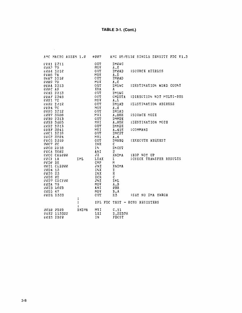
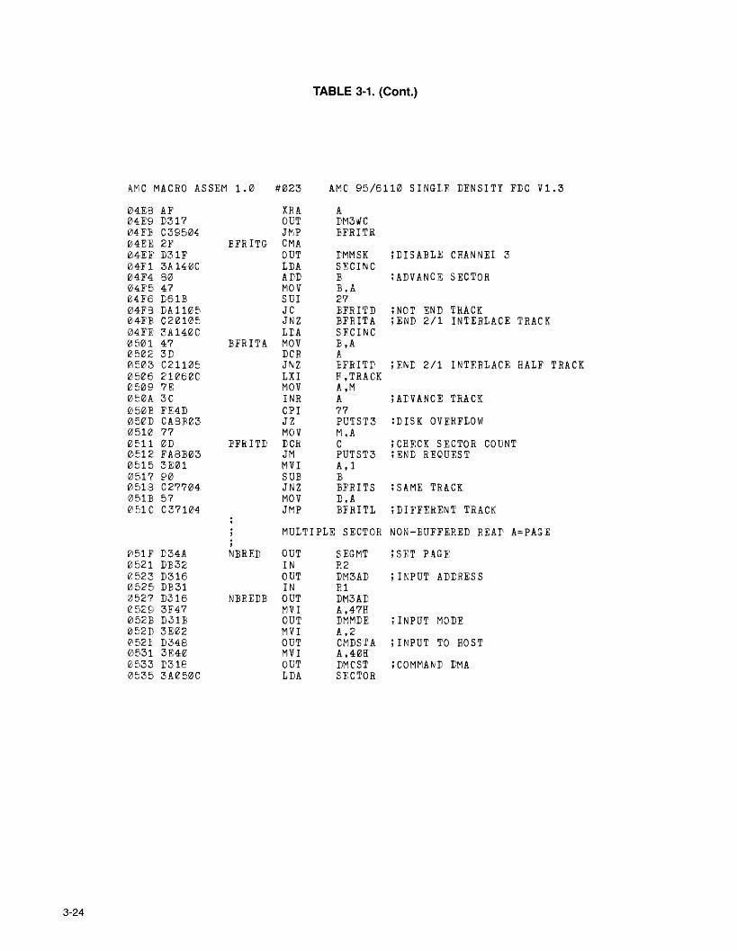
TABLE 3-1.
A~C MACRO ASSEM 1.e #e'e1 AMC 95/51 u;· SINGLE DENSITY FDC V1.3
17TJi' -~ '1 YPE EOU 611e ;SET TO 6110 OR 612eIF TYPE EQ 612f
TITLE 'AMC 95/6120 SINGLE/DOUBLE 11NSITY FDC V1.0'ELSETITLE ' AMC 95/6110 SINGLE DENSITY FDC V1.3'ENI'IFPAGE 43
;$-MACRO;SIM MACRO VALVE
MVI A,VALUEDB 3eHEN I'M
RIM MACRODB 20HENIM
HOST REGISTERS;
~e30 Re EQU :30h ;Ut\IT/PA~F
0031 R1 EOU 31H ;TRACK/MSB ADDRESSe;032 R2 EOU 32li ;SECTOR/lSB ADDRESSnl33 R3 EOU 33H ;COMMAND/STATUS
1771 REGISTERS
e000 IT-CST EOU 0 ;COMMANI'/STATUS0001 JiDTRK FOU 1 ;TRACKee02 FDSEC EOU 2 ;SECTOR0ee3 FDATA EOU :3 ;DATA-TRACK FOR SEEK
FDC REGISTERS;
e'048 CMDSTA EOU 48H ;COMMANT/STATrs~'049 RESET EOU 4gB ;SYSTEM 29 RESET004A SEGMT :E;QU 4AH ; ATDRESS PAGEe04F- CMl'RES EQU 4:BH ; COr-WAND RESETfl~AD I:RSEL EQU 4DH ;Ut\IT SELECT004E RELSE RQU 4EH ;SYSTEM 29 RELEASE
1771 COMMANDS

TABLE 3-1. (Cant.)
AMC MACRO ASSEM 1.0 #00:2 AMC 95/6110 SINGLE rENSITY FDC v1. 3
001'0 FRCIN EOU 0D0H ;FORCE STATUS Ie:e0A IiESTR EOU eAR ;RESTOREe.elE SEEK EQU lEE :SEEK TRACK0088 READ EQU B8H ;READ SEe TOR00A8 ViftITE EQU 0ASE ;wRITE SECTORe,0F4 WRTRK EQU eF4H ;WRITE TRACK005A STEP EQU ~AH ; S '1 EP IN0016 LDEED EQU 16E ; LOAD READ~,e10 UNLO:C EQU l0H ;UNLOAD HEAD
LMA POETS
EQU 10H ;CHANNEL 0 ADDRESSEQU l1B ;CHANNEL 0 WORD COUNTEQU l2H iCB:ANNEL 1 ADDRESSEQU 13H ;CHANNEL 1 WORD COUN'IEQU l4H ;CHANNEL 2 ADDRESSEQU 15H ;CHANNEL 2 WORD COUNTEQU 16R ;CHANNEL 3 ADDRESSEQU 17H ;CEANNEL 3 WORD COUNTEQU 18R ;COMMANr./STATUSEQU 19H ;REQUESTEOU lBE ;MODEEQU lCR iBYTE FLIP-FLOPEQU lDH ;RESETEQU lIH ;MASK
ERROR I~A SK S
0010 DM0ADere'll rM0WC0012 DM1AD0013 DM1WC0e:14 = DI"l2ADe'015 DM2WC10016 IM3AD0017 Drvl3WCe018 DMCST0019 I'MREQ001£ l'MMDEe01C rMBFF0·011' DMCLRei 01!' T'MMS K
;;
e·09C .RDMSK00FC \'v'RMSK
rQuEQU
9CHerCH
iREAI ERROR;WRITE ERROR
REQUEST }'ORMA'I'S
HOME
SETPAR
R0=UNITR3=REQUEST FUNCTION 0
1i0=UNITHl=TRACKR2=SECTOR(2-7TE BIT SET TO FORCE SIDE COMPARE - 6120 ONLY)
R3=REQUEST FUNCTION 1
3-3

A~C MACBO ASSFM 1.0 #e03
TABLE 3-1. (Cant.)
Arc 95/6110 SINGLE IENSITY FDC Vl.3
STATUSRe=tJNITR3=HEOu}~ST FUNCTION 2
CLRINTE3=REQUEST FUNCTION 3
INIDSKR0=UNITR3=REQU1Sl' FUNCTION 4
INTUNTR3=REQUEST FUNCTION 5
INTTRKR3:ohEQUIST FUNCTION 6
INTSECR3=REQUEST FUNCTION 7
READF0=PAGE(SEGMENT)h1==MSB DATA AI'DRESSR2=LSB DATA ADDRESSR3==REQUEST FUNCTIOr-.; 4X
WRITER0=PA~E(SFGMENT)
Fil=MS B DATA ADDRESSii2=LSB DATA ADDRESSR3=REQUF.ST FUNCTION 8X
EXF,CUTER0=PAG1(SEGMENT)Rl=MSB PROGRAM ADDRESSR2=LSB PROGRAM ADDRESSR3=REQt!EST FUNC'I'ION CX
X=0-63 (PLUS ONE FOR READ/WRITE SECTORS)(PLUS ONE TIMES 64 FOR USER PROGRAM LEN;TH IN BYTES)
STATUS IS RETURNED IN R3 AS FOLLOWS:BIT 0=SEEK CRC ERROR
l=SEEK ERROR2=LOST rATA OR WRITE FAULT3==READ/WRITE CRC ERROR(SET TO 1 FOR HOME AND 612e CONTROLLER - ELSE e FO~ d4=SECTOR NOT FOUND - SIDE FOR HOME ANr STATUS REQUESTS5=i\iiITE PROTECT6=DEVICE NOT READY7=OPERATION COMPLETE
3-4

A~C MACRO ASSEM 1.0 #1004
TABLE :~·1. (Cant.)
AMC 95/61110 SINGL1 DENSITY FIC V1.3
BITS 10-1 AND 2-4 ARE MUTUALLY EXCLUSIVE TBUS~
BITS 0 AND 2=ILLEGAL REQUEST FUNCTION1 ANt 2=TIME-OUT ON DEVICE BUSY OR LOST INTERRUPT
UNIT FORMAT:BI~' 0-1=UNIT 12-3
2=SItE0:fO, 1=13=DENSITY 0=SINGLE, l=DOUBLF4=RETRY 0=NONE. 1=9 FOR READ/WRITE. 5 FOR SEEK/HOMI5=BUFFERING 0=tISK TO HOST, l=DISK TO BUFFFR TO HOST6=INTERRUPT REQUEST 0=NONE, l=INTERRUPT HOST7=INTERLACE, 10=1/1, 1=2/1
eee'00cee
eeee
,PORG EQUHAMAD EQU
ORG
eeC0fOH
PORG
; PROGRMi: OhIGIN:DATA ORIGIN
IPL RAM TEST - UP/DOWN FF-f00 PATTERN-(B KEEPS ERROR CODE THROUGHOUT)
12012'0 3Ere100102 r30e0012'4 e1FIeFeee7 79121208 D33c000A 1101004eeer 21001~
1012112 2Be011 71e012 1B101213 7Aee14 B312015 C2H~0e;
0018 1604eelA 71,ee1B 910e'lC C2eS000e1Ji' 77~020 23121021 1B0,022 7Bee23 B212024 C21Ae0
FILL
UPF
MVIOUTLXIMOVCDTLXILXIrcx~OV
DCXMOVORAJNZMVI["iOVSUBJNZMOVINXDCXMOVORAJNZ
A,FRCINFrCST :TERMINATE 1771 ACTIVITYB,0FFFRA,llR3 ;I~ITIALLY SET ALL ERRORSD,1024H,RAMAD+1024H ;INITIALLY FILL ALL RAM WITH FF~,c
DA ,l~
F.E'II,LI:.4A,M jCHECK FOR FF AND SET 100 UPCPROMM,AHIA,EDDPF
3-5

AMC ~ACRO ASSFM 1.12 #005
TABLE 3-1. (Cont.)
AMC 95/5110 SINGLE DENSITY FDC Vl.3
0027 21000C0fZ2A 1604002C 71002D 137ee'2E C269000031 710032 230033 1E0034 7A0035 1330036 C34000003900'39 C37001
I·XIf"~VI
UPZ MOVORAJ'\JZMOVINXDCXMOVORAJMPORG
RF'TURN JMP.
E,RAMADD,4A,M ;C3ECK FeR 00 AND SE~ FF UP/<PROMM.CEDA,DEDNI39BCMLLP ;FOR USER PROGRAM RETURN
INTERRUPT 7.5
UPZD,4E jCHECK FOR FF AND SET 00 DOWNA.MCPROMM,AI,A,DEDNFH,RAMAI:+1024D,4H ;CHECK FOR 021 AND SET FF DOWN.A,MAPROMt"l.CDA,DEDNZ13.flEHA,13
3-6
003C Dl003D L1300003F C9efl40 C22C0e,0043 1604e045 2130fl46 7R0047 910048 C269000e'413 77004C 113004D 7Aee4E 133004F C245000fZ52 2100100055 16040057 2130058 7:E12059 137005A C26900005D 71005E 1130e5F 7AefZ'60 133ee61 C2570·0e064 2160E~H~66 78
Dr.-I
DNZ
POPINRETJNZMVIDCXMOVSUPJNZMOVICXMOVORAJNZLXIMVIDCXMOVORAJNZMOVDCXMOVORAJNZMVIMOV
I:FDCST
;CLEAR rtST RETURN

TABLE ~.-1. (Cont.)
AMC MACRO ASSljM 1.0. #00.6 AMC 95/6110 SINGLE DENSITY FDC lJl.3
0.12,67 D333 OUT 1\3 ;SET NO RAM ERROR
IPL PROM TEST UP/DOWN CHECKSUM AND COMPARE;
e'069 lle'A~n PROM LXI D,ENTST006C 210.004 LXI H,H'24e06F 4D MOV e,L0070 lA UPC LDAX D ;CHECKSUM UPWARDS12071 13 INX re072 81 ADD Ce,e73 4F MOV C,A0074 2B DCX Hee7!5 7C MOV A,E12076 B5 ORA L12077 C27e00 JNZ VPC007A FE XCHGelO7B 1604 MVI t,4007I' 91 SUE C ;COMPLEMENT CHECKSUM007F 4]' MOV e,Aee'7F 2B DNC rcx H10080 7E MOV A,M ;CHECKSUM rOWNwARDS0.081 81 ADD C0.1282 4F MOV C,A00.83 IB DCX D01284 7A MOV A,r120.95 B3 ORA E120.86 C27Fe0 JNZ rNC008S Bl ORA Ce08A C2,9300 JNZ rMA008D 78 MOV A,Be,08E E6er ANI erE1210912 47 MOV E,A10091 r333 OUT R3 ;SET NO PROM ERROR
IPL Df"1A TFS ~~ - MEMORY/MEMORY TrtANSFER;
ee'93 D31:C rMA OUT DMCI,R ;RESET I'MA(1'1295 eEFF MVI C,0IFP.0097 l10A01 LXI I,ENTST0~:)9A 21e00C LXI E,RAMADee9D 79 MOV A,Ce09E r311 OUT IM0\IJ'C ;SOURCE ~ORD COUNTe'0A0 AF XRA A
3-7
3-8
TABLE 3-1. (Cant.)
AIv1C MACHO ASSEM 1.'0 #'0'07 AMC 95/6110 SINGLE DENSITY FDC V1.3
(:,e'A1 D:311 OUT DM0WCe0A3 713 MOV A,Et;e'A4 13112 OUT D~eAD ;SOURCE ADDRESSe;eA6 7A MOV A,t00A7 D310 OUT DMeAD0eA9 79 MOV A,C0eAA D313 OUT tMHiC ;DESTINATION WORD COUNTeeAC AF XRA Aee,At D313 OUT 1:Ml~C
e0AF D348 OUT CMDSTA :DIRECTION NOT t"lULTI-EUS0'0]1 7t MOV A,Le0B2 1:312 OUT DM1AD ;DJ:;STINAT'ION AD1RESSe'0'134 7C MOV A,He0B5 D:312 OUT IM1AD0eB7 3E88 ~VI A,88H ;SOUhCE MOLE00]9 D3113 OUT DMMDE0~13B 3£85 MVI A,85H ;DESTINATION MODEee13D D3113 OUT DMMDE0013F 3E41 MVI A,41H :COMMAND0eCl D318 OUT tMCST0eC3 3F0'4 MVI A,4ee'C5 D319 OUT I:MREQ :EXECUTE REQUEST00C7 ~c INR C0lOC8 D1318 IN r-rvJ CS Te0CA E602 ANI 2eecc CAE0ee JZ ENI-MA ;EOP NOT UPe0C:F lA I:ML LDAX I ;CRECK TRANSFER RESULTSeeD0 BE CMP M0eD1 C2E00e JNZ ENDMA00D4 13 INX D-eeD5 23 INX H01016 lOr DCR c120D7 C2CF00 JNZ tML0eDA 79 MOV A,130er'13 E6013 ANI eBHe:0DIi 47 MOV B,A0'0DE D333 OUT R3 :SET NO DMA ERROR
IPL FDC 'rEST ECHO REGISTERS;
001£0 0EeB ENDMA MVI C,lle0E2 113322 LXI D,2233HeeE5 D13e0 IN FDCST

TABLE ~J-1. (Cant.)
liMe MACRO ASSEM 1.0 #0es A!"1C 95/6112 SINGLE DENSITY FDC V1.3
eeE7 1F RAR,e18 fAe.A01 JC ENTST ;EUS Y00FB 79 MOV A,e20EC L'3i01 OUT FDTRK ;SET TRACK REGISTERZ0EE 7A MOV A,DQ'e,EF D302 OUT ELSEC ; SET SECTOR rlE:}ISTER00F1 7B MOV A.EeeF2 D302. OUT FDATA ;SET DAlIA REGISTER0elt'4 DBe1 IN FDTRKee:F6 91 SUB C00F7 4F ~OV C,A ;ChECK TRACK REGISTEReea's DPe;2 IN FDSEC0~FA 92 SUB :D00FP, P1 ORA C ;CHECK SECTO R REGISTERe~FC 4¥ MOV e,A00FD IE 02 IN FIATAe0Fl 93 SUB Eflee Bl ORA C ;CHECK DATA hEGISTEli0101 C20A01 JNZ ENTST0104 79 MOV A,E0105 Ese7 ANI 70107 47 MOV B,A0108 D333 OUT R3 ;S1T NO Frc ERROR
INITIALIZE \,I,ORKING STORAGE;
e10A 312e:ec ENTS1' LXI SP,STACK0101 AF XRA Ae.'leE D301 OUT FDTRK ;SET TRACK 00110 D34E OUT CMIRES ; CLEAR COMMAND FF0112 2LFFFF LXI H.-'1e115 2201e,c SHLD POSN ;CLEAR UNIT POSITIONSel18 22030C SHLD POSN+2011] 23 INX H011C 2C INR Le.·llD 22e50C SHLD SECTOR ;SECTOR 1 , TRACK e'0120 32130C STA INTFLG ; NO I NTERRup'r REQUEST0123 3C INR A0124 32140C STA SECINC ;1/1 INTERLACE0127 3108 MVI A,8012P 320S0C STA RFCr..T ;RFTRY COUNT-1f12C e7 ELC0121) 4E' MOV C,A
3-9

3-10
TABLE 3-1. (Cont.)
AI":C MACRO ASSEM 1.O #0129 AMe 85/6110 SINGLE DENSITY FDC V1.3
e'12]; 32070C STA l'NIT ;'GNIT 0 WITH RETRYIF TYPE EQ 6120MVI A,READSTA IOCO:DE ;SET NO SIDE COMPARE FOR READ/WRIT'EMVI A,0CHELSE
iZ 1~)l 3E04 MVI A,4ENDIF
e133 D34D OUT DESEL :UNIT ZERO, SINGLE I,ENSITY, SIDE 012135 3E7E' MVI A,1270137 320e0C STA SECLEN ; SECTOR LENGTR-le13A 21E102 LXI H,FUNTN013D 220B0C SHLD JPTAB ;MISCELLA~EOUS FUNCTION JUMPe'140 211F05 LXI P,NFREI'e·143 22fz,r0C SHLD JPTAB+2 ; NON-BUE'FERED READ JUMP0146 21C505 LXI H,NJ3RIT014S 220I0C SHLD JPTAE+4 ;NON-BUFFERED WRITE JUMPe14C 21340'6 LXI H,PGMRD014F 22110C SHLD JPTAB+6 ;UStR PROGRAM READ JUMP12152 78 ~OV A,Be153 B7 ORA A0154 C26701 JNZ SETCOM ;GO SET COMPLETE ON IPL ERROR0157 RIMe158 B7 ORA Ae;159 F26906 JP BOOT ;GO BOOT SYSTEM 29
STATes RFQUEST C=UNIT;
e15C CI9201 STREQ CALL SELUN ;SET UNIT STUFFeU:'F 79 MOV A,C0160 C1:6202 CALL READY0163 0F SIDSTA RRCe164 3120ec ILLCOM LXI SP,STACK0167 F68e SE'l'COM ORI B0H ; SET COMPLETEe169 D333 OUT H.3 ;TELL USERe16E 3A13ec LDA I NTFLGe16E 11348 OUT CMLSTA ;SET/CLEAR INTERRUPT217e DB48 Ct"IDLP IN CMDSTA ;CHECK FOR USER COMMANDe172 B7 ORA Ae173 F27001 JP CMDIP:2'176 D:34B OUT CMDRES ;CLFAR COMMAND FFe178 DB33 IN R3 :FETCH REQUESTe'17A 5F MOV E,A

TABLE 3-1. (Cant.)
A. r\l~ C ~ACRO ASSE~ 1.e' #01e AMC 95/5110 SINGLE DENSITY FD,C Vl.3
Z17B E63F ANI 3FHe17D 4F MOV C,A ; COUN'I'-le17E AB XRA E017F 07 RLC018e 07 RLC12181 07 RLCe182 5] MOV E,A12183 AF XRA A0184 57 MOV D,A0185 I:31D OUT DMCLR ;RESET DMA0187 21e:B0C LXI E,JPTA:BQ18! 19 rAD De'18B 5£ MOV I,M ;FETCH VECTOR JUMP018C '"''':t If\X B':::,-,
((lSD :,5 MOV D,M12;181 DB30 IN R0 ;PAGE/UNITelS10 EB XCBGQ191 Eg PGRL ;GO TO JUMP ADDliESS
SELECT U~HT AND SFT VARIABLES C=lJt\iI T;
0192 79 SELUN MOV A,e01S3 3207e,c STA rNIT12196 21e70C SETUN LXI H,UNIT0199 46 MOV B,M ;SAVE PRIOR tR1V~
01S'A 71 MOV ~,c
fcH9B 79 MOV A,C019C E608 ANI ee'l S'E 17 RAL019]' 17 RAL121A0 17 RAL01Al 17 RALf'lA2 C67F ADI 12701A4. :32000C 5'1'A SECLEN ;SECTOE LENGTH-lelA7 78 MOV A,e01AS E61fc ANI 112801AA 0F RRCelAE 32080C STA hFCt\T ;RFrRY COUNT-lelAE 79 MOV A,C01AF 07 RI,CelB0 F6e'1 ANI 1121132 3C INR AelF3 3214e,( 5'I'A SEeINC ;INTERLACE
3-11

TABLE 3-1. (Cant.)
AMC ~ACRO ASSEM 1.0 #ell AMe 95/6110 SINGLE DENSITY FDC Vl.3
01B6 79e'lB7 0F'01B8 E62001BA 32130C01BD 7901BE l1C50501Cl 211F'05,e1C4 E62001C6 CACFele1C9 113704e'lCC 2107e301CF' 220D0C01D2 FB01D3 22e,Ff:CelD6 79
e, 1D7 E6e:701I9 EE04
e,lDB r34D01DD E60301I:F 5Fe1Ee 160e,01E2 2101ec01E5 19e1"E6 7E01E7 D3e'l'll E9 7SelEA A901EB E60301EI CB01EE 7E01EF lf10elF1 CDB=02elF4 C30004
MOVRRCANIsrr'AMOVLXILXIANIJZLXILXI
SETVEC SHLDXCEGSHLDMOVIFANIXRIELSEANIXRIENDIFOUTANIMOVMVILXIDADMOVOUTMOVXRAANIRZMOVMVICALLJMP
p, ,C
20aINTFLG ; INTERRUPT REQUESTA,Cr, NBRITH,NBRED20.HSETVECD,BFRITH, B]'REDJPTAP+2 ;SET JUMP TABLE ArDRESSES
JPTAB+4A,CTYPE EQ e120f:F'H0CH
74
DRSEL ;SELECT DRIVE3E,AD,0E. POS NIiA,M ;CURRENT UNIT POSITIONFDTRK ;TELL 1771A,CB
;SAME DRIVEA,Mr,UNLODLOADA ;U~LOAD HEADPOSNC ;AND POSITION NEW DRIVE
3-12
elF7 CL1502
; hOME REQUEST C~UNIT
,HMREQ CALL HOME
IF TYPE FQ 6120

TABLE :~-1. (Cont.)
AtvlC MACRO ASSEM 1.0 #1012 AMC 95/6110 SINGI,E :CENSI'!'Y FDC V1.3
INR AENDIF
e1FA E6F9 PUTST1 ANI 0F9H ;PUT STATUS TYPE I01:F'C 57 MOV D,A01FD 73 MOV A,E01FE 320510C STA SECTOR0201 7A MOV A,T:~202 0F RRCe2e3 0F RRC02104 E606 ANI 60206 132 ORA D0207 E616 ANI 0E6He209 5F MOV F,A02~A 7A MOV A,D02013 E601 ANI 1e210D 07 RLCe20'E 07 RLC0210]' 107 RLC0210 07 RLC0211 133 ORA E0212 C36301 JMP SIDSTA
HOME FUNCTION C=UNIT;
10215 CDS201 HOME CALL SELUN0218 0601 MVI :E,1021A AF' XRA A02113 32060C STA 'rRACK021E 3A080C LDA RECNT0221 0F RRC0222 320A0C STA SKTRY022:, CD3E02 HOMEL CALL EESTORE10228 F8 RM ;NOT REAry0229 F604 ANI 4,02213 713 MOV A,E1022C C0 RNZ ;GOOD HOME0221) 210A0C LXI H,SKTRY0230 35 DeR M0231 F22502 JP HaMEL ;RETRY0234 CS~ RET
RESET NON-BUFFERED ADDRESS - - FALL INTO RESTORE - -
3-13

3-14
TABLE 3-1. (Cant.)
~MC MACRO ASSEM 1.0 11013 AMC S'E/611~ SINGLE DENSITY FtC V1.3
~~i2 ~,~. 2A00ZF' RS~BA IHLI BUFFe233 7D r-;OV A.Le239 [316 OUT DM3ADe23E 7C MOV .A,He23C D316 OUT I'f";3AD
EXECUTE RESTORE
023E 3A070C RESTORE LDA UNIT0241 CD6202 CALL REAllY0244 F3 RM ;NOT READY2245 3A070C LIA UNIT0,248 F603 ANI :3e'24A 5F MOV E,Ae24:E 1600 MVI D.eei24:r 21010C LXI E,POSrx0250 19 DAD D0251 72 MOV M,D ;SET POST ION ZERO0252 l60A MVI r,REsTR0254 CD8702 CALL ISSUE02f7 E6IC ANI 0DCE0259 5F STSID MOV E,A0'25A DB48 IN CMDSTA025,C k61e }.N I 10H225F. 07 RLC02E'.F E3 ORA E0260 51' MOV E,A0261 CS RET
CHECK READY FOR TYPE I COMMANDS
IF TYPE EQ 6120READY ANI 0Fa
XRI lCBELSE
0262 E607 READY ANI 7e264 EE0C XRI eCE
ENDIFe266 D34I OUT rESEL0'268 57 ~OV I,A0269 3ED0 MVI A,FRCIN026B D300 OUT FLCST026I E5 PUSH H

TABLE :J-1. (Cant.)
AfV:C MACRO ASSEM 1.0 #014 AMC 95/6110 SINGLE DENSITY FDC V1. 3
1226F E1 POP P026]' E5 PUSH H12270 E1 POP H0271 DB00 IN FDCST0273 E6C0 ANI 0C0H12275 CL5902 CALL STSID12273 7A MOV A,D
IF TYPE EQ 6120ANI eFHELSE
0278 E607 ANI 7EN:DIF
~)27B D34D ou'r BRSEL027r 7B ~OV A,E1227E B7 ORA A027F C9 RET
LOAD HEAr FOR READ/~RITE
12280 1616 LOAD MIlI r,LBHED12282 3AI2'60C LDA TRACK12285 D303 LOADA OU'f FDATA
ISSUE COMMANr IN D
0287 1E00 ISSUg Mill E,012,28£ 1t ISSUEA DCR Ee29A CAA912,2 JZ ISSUEC :BUSY028I DB01Z IN FDCST028F 1F RAR122912 DA8902 JC ISSUEA2293 SIM 1BH ;CLEAR INTERRUPT0296 7A MOV A,D12297 D3120 ISSUEE OUT FDCST ;ISSUE COMMAND02,99 FB EI1229A 11De07 ISSUED LXI I',212001229D AF ISSUEB XRA A1229E, 3D I 5S D,EF feR A029F C29E02 JNZ ISSUEF ;liAIT FOR INTERRUPT02A2 1B DCX D122A3 7A MOil A,D02A4 E3 ORA F.02A5 C29D02 JNZ ISSUEB
3-15

AMC MACRO ASSEM 1.0 #015
TABLE 3·1. (Cont.)
AMC 95/6110 SINGLE DENSITY FDC Vl.3
el2A8 F302A9 7802AA 32050C02AD 3E06e2AF' C36401
1HISS DEC !"IOV
STAtylVIJ'MP
A,BSECTORA,6ILLCOM ;NC INTERRUPT
SET PARAMETER REOUEST C=UNIT, BL=TRACK/SECTOR
e~'B2 DB3102B4 6702]5 DB32
02B7 6F02B8 22050C
02BB CD960102BE AF02BF C36701
;SRTPAR
BRTN
INtolOVINIE TYPEt"IOVANII~DIF
t"lOVSHLDIE TYPE~lV I~10V
ANAELC~10V
MOVANIORAULCORASTAENDIFCALLXRA~rMP
R1E,AR2EQ 6120B,A7FH
L,ASECTORFQ 6120L,80fiAtBL
E.AA,C4B
LIOCODE
SETUNASETCOM
;STRIP COMPARE FLA~
;STRIP SIDE FLAG
;SET CONDITIONAL READ/WRITE
:SET U~IT STUFF
CLEAR INTERRUPT REQUEST
3-16
02C2 AF02C3 4702C4 AF02C5 D34802C7 7802C8 F68002CA D333
,CLRINT XRANOI NT t10V
XRAOUTI"!0VORIOUT
AB,AACMDSTA ;CLEAR INTERRUPTA,BS0HR3

TABLE ~1·1. (Cant.)
.AMC MACRO ASSEM 1.0 #016 AMC 95/6110 SINGLE DENSITY FDC Vl.3
02CC C37e01 JMP CMDLP
RETURN UNIT REQ.UEST
02CF 3A070.C IwrUNT LDA UNITe2I'2 C3C302 JMP NOI NT
RETURN TRACK REQUEST;
e·2Dt: 3Ae60C IN~~TRK LDA TRACK0.21'8 C3C30.2 JMP NOINT
RETURN SECTOR REQUEST;
0.2r:E 3Ae50C I N~~ SIC LLA SEC'TORe2DE C3C302 JMP NOINT
REQUEST CODES (2;-63;
02El 59 FUNTN MOV E,CQ12F2 4F MOV C,A02E3 7B MOV A,E0214 FE08 CPI 802E6 3EQl5 MVI A,502E3 D2670.1 JNC SETCOM ;ILLEGAL FUNCTION02EB 16e0 MVI D.002ED 21F7e'2 LXI H,V:ECTAB02F0 19 DAD D02Fl 19 DAD re2F2 5E MOV I,M02F3 23 INX H0.2F4 56 MOV r,M02F5 FB XCEG02F6 E9 PCRL02F7 F701 VECTAB DW HMR:EQ ;HOME REQUEST02F9 B202 DW SFTPAR ; SET I/O PARAMETERS02FB 5C01 DW STR:~Q ;STATUS REQUEST02FD C202 Dw CLRINT ;CLEAR INTERRUP'I' REQUEST02FI CEe,6 DIN INIDSK ;INITIALIZE DISK REQUESTe301 CF02 DIN INTUNT ;INTERROGATE UNIT0.303 D502 DW I NT1rRK ;INTERROGATE TRACK0.30.5 D.B0.2 pw' INTSEC ;INTERROGATE SECTOR
3-17

A~C MACRO ASSEM 1.0 #017
TABLE 3-1. (Cont.)
AMC 95/61112 SINGLE tENSITY FDC Vl.3
MULTIPLE SECTOR BUFFERED READ A=PAJE
123rl7 D34A0309 3F012030B D31e030I 3E12F030F'1:31ee311 DB320313 D3120315 DB310317 D3120319 AFe31A 320sec031D 3E:ee03l:F' D3160321 3E12F0323 D3160325 3A000C0328 6Fe·329 D311032B AFrl32C D311e'32E 7D032F D3170331 AF03,32 D3170334 57e335 3F980337 D31B0339 31850331' D31B033D 3E57033F D31B12341 3,A0512C0344 471234:: CDEF030348 FAFA01034E AFe'34C D348234F 780341' D30203,51 3ED0e353 D312e
3-18
BFRED OUTMVIOUTMVIOUTINOUTINOUTXRASTA
BFREDR MVIOUTMVlOUTLtA~OV
CUTXRAOUTMOVOUTXRAOUTMOVMVlOUTMVIOUTMVIOUTLDAMOV
BEREDL CALLJM
BFREDS XRAOUTMOVOUTMVIOUT
SEG~T : SET PAG EA,BUFF-BUFF/256*256IDM0AD :M/M SOURCE ADDRESSA,BUFF/256:CMeADR21M1AD ;M/M DESTINATION ADDRESS.Rl:DM1ADARETRY ;SET READ RETRYA,BUFF-BUFF/256*256DM3AD ;INPUT ADDRESSA,BUFF/256:CM3ADSECLENL,ADM0~C :M/M SOURCE WORD COUNTAI~t"0~i CA,LfM3WC ;INPUT WORt COUNTA:OM3WC:[',AA,98RfMMDE :M/M SOURCE MODEA,65HfMMDE ;~/M DESTINATION MODEA,57HDMMDE ;INPUT MOLESECTOR:B ,APOSITN ;READ LOOP B=SECTOR. C=COUNT, (HL);POSITIONPUTSTI.A.CMDSTA ;INPUT TO LOCAL BUFFERA, :p.FDSEC ;D1SIRED SECTORA,FRCINFDeST ;REQUEST STATUS I

TABLE 3·1. (Cont.)
A.MC MACRO ASSEM 1.0 #018 AMC 9=/6110 SINGLE DENSITY F:DC V1.3
Q\355 3E4.0 t"VI A,40H0357 D318 OUT rMCST ;COMMANI' DMA0'~~59 3107 MVI A,7e35B D31F OUT rrviMsK jEt\ABLE CHANNEL :3035D SIM 1BH0360 DB~·0 IN FrCST jHEAT' LOAr STATUS0362 E620 ANI 20B0364 CC8002 CZ LOAL
IF TYPE FQ 6120LDA IOCODEELSl;
0·367 3E88 t"VI A,RRADENDIF
21369 CD9702 CALL ISSUE]~ jEXECUTE READe36C E6PC ANI RLMSK0361£ CAA2e3 JZ BFREDG ;GOor READ0371 IA8C03 JM PUTST2 j NOT REArye;374 57 rv:OV I,Ae.375 3E~F MVI A,0FHe377 D31F OUT rMMSK j:DISABLE CEANN EI. 3e'37S1 210S'0C LXI H,RETRYe37C 34 INR Mrt37I' 3A0f:eC LIA BECNT038e BE crllip M0·381 7A. MOV A,De'382 IA8C03 JM PUTS'1'2 jENI: RETRY0385 CD3E02 CALL RISTORFe338 C31De3 Jr1P BFREDR038B AI PU~~S'1'3 XRA Ae'38C 57 Pu~~srr2 MOV I,A ;SAVE SFCIra R/ SF'I' REAt-WRITE STATUSe·33D 73 MOV A,Be;:~8E 32e50C SITA SECTOR03Pl 7A MOV A,t0392 E62e, ANI 20H0394 0F REC2'7.0k 21F RRC~v'-
fZ3·96 eF R:RCe397 B2 ORA re398 E6IC AI\ I eICE039A 57 MOV D,A039B E61C ANI lCBe39f 82 AfD D02·9E eF RRC
3-19

AMC MACRO ASSEM 1.0 #019
TABLE 3~1. (Cant.)
AMC 95/61112 SINGLE DENSITY FrC Vl.3
039F C367l2103A2 32 lZ'90C03A 5 2]'03A6 D31F03A8 3AlZe0C03AB D31303AD AF03AE D31303]12 3F4103B2 D31803]4 3E0403:E6 D34803B9 D31903BA DB1Se·3] C Ee 122C?3BE CA:BA0303Cl 3A140C2:3C4 80e3C 5 47123C6 D61Ee3C8 DAE103123CB C2D10303C E 3A 140C1231:1 47e3D2 3re3r3 C2E103e.3D6 211Z6ece3D9 7E03IA 3C03IB FE4re3DD CA8BlZ·3123],0 7703El eL03,E2 FABB0303E5 3E0l03F7 912'e3EB C24B03Z3EB 5703EC C34503
BFREIG
BFREn..
BFRITA
:BFRFDD
.IMPSTAeMAOUTIDAOUTXRAOUT~~V IOUT~'JV IOUTOUTINANI~J ZIDAADDMOVSUI~r c~rNZ
]~DA
~10V
])CR~rNZ
LXI~10V
INRCPI~T ZMOVrca~rM
~1 vISUB~rNZ
~lOV
J:MP
SET COMRETRY
DMMSKSECLENt~niC
ArM1v.'CA,41BDMCSTA,4CMDSTADMREODMCST
BFRED~r
SECINC:EB,A27BFRE:DDEFREDASECINCP,AABFREDDE,TRACKA,MA77PUTST3M,ACPUTST3A,lEBFREtSD,AEFltFDL
jRESET RETRY
;DISABLE CHANNEL 3
jM/M DESTINATION WORD COGNT
:COMMAND DMA
jLOCAL BUFFER TO EOST;REQUEST DMAjWAIT DMA TRANSF1R
jADVANCE SECTOR
;NOT END TRACK;END 2/1 INTERLACE TRACK
jEND 2/1 INTERLACE HALF TRACK
jADVANCE TRACK
;DISK OVERFL~'t
;CHECK SECTOR COUNT:END REQUEST
;SAME TRACK
jDIFFERENT TRACK
HE-POSITION TRACK
3-20
e3EF 3A07lZC POS ITN I,IA UNIT

TABLE 3·1. (Cont.)
AMC MACRO ASSEM 1.0 #020 AMC 95,/6110 SINGLE DENSITY FIC V1.3
03F2 E603 ANI 303F4 5F MOV E,A02F5 1600 MVI D,003F7 21010C LXI H,POSNe3FA 19 DAD D03FB 3A060C LDA TRACK03FE BE CMP M0'3F1' C5 RZ0400 3A080C POS ro-IC LDA RFCNTQ~403 eF' RRC0404 320A0C STA SK~rRY ;RETRY COUNTei407 7F POSNA MOV A,M0408 :87 ORA A0409 F'A2C04 JM POSND ;INITIA1 REFERENCE - RESTORE FOR SYNC040C 3A070C LDA UNIT040F CD6202 CALL READY0412 F8 RM0413 3Af2:60C LT.A TRACK0416 D303 OUT ]'DATA0418 77 MOV M,A ;UPDATE POSITION0419 161E MVI I ,8 EEK041B CD8702 CALL ISSUE041E E698 ANI 9sa0420 C8 RZ ;Goo:t SEEK0421 FS RM iNOT READY04,22 5F MOV E,A0423 3A0A0C POS NB LLA SKTRY0426 3D DCR A0,427 320'A0C STA SKTRY042A 71' MOV A,Ee421' F8 RM iEND RETRY042C CD3:E02 pes ND CALL RESTORE042F E604 ANI 40431 C20704 JNZ POSNA0434 C32304 JMP POSNB
MULTIPLE SECTOR BUFFERED WRITE A=P AG- F;
0437 r.34A BFRIT OUT SEGMT ;SET PAGE0439 3E00 MVI A,BUFF-BUFF/256*256043:8 r'312 OUT DM1AD ;M/M DESTINATION ADDRESS043D 3E0F MVI A,BUFF/256f2:43F D312 OUT DMIAD
3-21

TABLE 3u 1. (Cant.)
P.MC MACRO ASSEM 1.0 #1221 A~'C 95/6110 SINGL1 IENSI'lY FDC 111.3
~'441 LB32 IN H22443 T31e OUT I'M0AL jM/M SOURCE ATLRESS0445 LrB31 I~ 11'.1e447 D31e OUT I:M0AD2449 3Eee MVI A.BUFF-BUFF/256*25B044B D316 OUT l'M3AD jOUTPUT AtDRESS044D 3EeF MVI A,BUFF/256044F D31E OUT IM3AD2451 3A12120C Lr,A SICLEN0454 6F MOV 1.,A0455 D31:3 OUT I:M HiC jM/M rESTINATION wORD COUNT0457 AF XRA A12453 D313 OUT DM1WCe45A 7I MOV .A .L1245,"8 D317 OUT I1t":3WC jOUTPUT WORD COUNTe45D AF XRA Ii1245,1 r317 otT IM:3WC12460 57 MOV II,A12461 3E88 MYI A,83He4f3 D31B otT IMMr'E jM/M SOURCE ~O:CE
12465 3ES5 ~VI A,9:',H04E7 D31B OUT I'MMDE :M/M DESTINATION MODE0469 :3.J!;5B MVI A,5BH04EB D31B OUT I'MMLE j OUTPU!' MOt,Ee461 :3Ae50C LDA SECTOR04710 ·17 MOV :LA0471 CLEFe3 BERITL CALL POSITN nlRITE LOOP ]=SECTOR, C=CCUNT, (HI)=POSITION12474 :~AFA01 JM PUTSTl12477 :3A000C BFRITS LDA SEC LEN047A :0311 OUT tM0WC j M/M SOURCE \vORD COUNT047C ,!F XRA Ae47D :32090C STA RETRY jSET RETRY COUNT12'480 :0311 OUT t!"'0WCe482 :3E41 MVI A,41H12'484 :D318 OUT IMCST jCOMMAND DMA12486 :3E06 MVI A,6e488 :0349 OUT CMDSTA :HOST TO LOCAL BUFFER048A :3E04 MYI A,4e48C D319 OUT Irv:REQ jREQUEST rMAe43E :OB1S BFR ITIN IN DMCST ;WAIT DMA TRANSFERe490 I602 ANI 212492 GA8F04 JZ :EFHITWe495 AF BFRITR XRA A.
3-22

TABLE :~-1. (Cont.)
A~C MACRO ASSEM 1.e
0496 D3480498 73e49~ D302e49B 3ED0049I: D300049F 3F4004A1 D31804A3 3E0704A5 L31F04A704AA DB0004AC EB20'e·4AE ccse02
~\4:P1 31:A8
24B3 CI9702((4B6 FBtCe4B8 CAEE0404]B 5704BC I,6cee4BE 7A04BF C28C0304C2 3FeIe'4C4 I:31F04C6 21090C04C£' 34e4CA 3A080Ce'4C D BEe4CE 7A04CF FA8C03,04D2 CD3E0204I:5 CI'EF03e4D8 FAFAe'l04IB 3E00e41'L D316e'4DF 3Ee'Fe'4.:E1 D31604:1'"'3 3A000Ce4E6 D317
AMC 95/6110 SINGLE tENSITY FDC V1.3
CMDSTA ;OUTPUT FROM LOCAL BUFFERA,BFDSEC ;DESIREr SECTORA,FReINFDCST ;REQUEST STATUS IA,40HDMCST ;COMMAND DMAA,7rMMSK ;E~AELF CEANNEL 31BHFDCST ;l:iEAD LOAD STATUS2,0HLOADEQ 6120IOCODE20H
#022
OUTMOVOUTMVIOUTMVIOUTMVIOUTS1MINANICZIF TYPELDAORIELSE~VI
ENDIFCALLANIJZMOVANIMOVJNZMVIOUTLXII~R
LDACMPMOVJMCALLCALLJMMVIOUTMVIOUTLriAOUT
A,WRITE
ISSUEE ;EXECUTE WRITE'lRMSKBFRITG ;GOOD WRITEI,A0C0HA.DPUTST2 ;NOT REAry OR WRITE PROTECTA,0FHDMMSK ;DISABLE CHANNEL 3H ,RETRYMBECNTMA,DPUTST2 ;END RETRYRESTOREPOSITNPUTST1A,BUFF-BUFF/256*256TM3AD ;RESET OUTPUT ArrRESSA,BUFF/256DM3ADSECLENr~3WC ; RES ET OUTPUT WORD COU NT
3-23
AMC MACRO ASSEM 1.0 #023
TABLE 3·1. (Cant.)
AMC 95/6110 SINGlF DENSITY FDC V1.3
04E3 AF04E9 D31704FB C3950404EE 2F04EF D31F04Fl 3A140C04F4 8004.F'5 47e4F6 t61B04F9 DAl10504FP, C2010504FE' 3A14eC0501 470502 3D0.503 C2110505e6 21060Ce'509 7Ee'50A 3Ce'50B FE4D050D CA3B030510 770511 0n0512 FA8B030515 3E010517 900518 C27704051B 57051 C C37104
XRAOUTJrvlP
EFRITG CMAOUTLDAADDMOVSUIJCJNZLfA
BFRITA MOVDCRJ~Z
LXIMOVINRCPIJZMOV
EFRITI; DCRJMMVISUBJNZMOVJMP
ADM311lCEFRITR
IMMSK iDISABL.l: CHANNEL 3SECINCB ;ADVANCE SECTORB,A27EFRITD ;NOT END TRACKBFRITA iEND 2/1 INTERLACE TRACKSFCINCB,AAEFRITD iEND 2/1 INTERLACE HALF TRACKF,TRACKA,MA iADVANCE TRACK77PUTST3 ;DISK OVERFLOWM.AC iCHECK SECTOR COUNTPUTST3 ;END REOUESTA,lBBFRITS ;SAME TRACKD,ABFRITL iDIFFERENT TRACK
MULTIPLE SECTOR NON-BUFFERED READ A=PAGE
3-24
051F D34A0521 DB320523 D3160525' DB310527 D31605,29 3F47052B D31B052D 3E02e'52I D3480531 3E400533 :D3180535 3Ae50C
,NBRFD OUT
INOUTIN
NBREDB OUTMVIOUTMVIOUTMVIOUTLDA
SEGMT ; SET PAGI'R2DM3AD iI~PUT ADDRESSRlDM3ADA,47HDMMDE ;INPUT MODEA,2CMDSTA iINPUT TO HOSTA,40HDMCST i COMMAND DMASECTOR

TABLE ~l·1. (Cant.)
AMC MACRO ASSEM 1.0 #024 AMC 95/6110 SINGLE DENS I '1'Y FDC Vl.3
l!:38 47 MOV B,A0539 ~.F XRA A053A 320800 STA BE'fRY i SET READ RETRY0~:3D CDEF03 NBREDR CALL POSITN0540 FAFA01 JM PU'fST 10~43 3A000C N]3R EDL LBA SEeLEN0=-:46 D317 OUT rM:3WC ;INPUT ",TORD COUNT0548 AF' XRA A"1549 D317 OUT DM3'WCe54B DB16 IN DM3AD054D 6F MOV I" .A054.1) DB 16 IN DM3AD0550 67 MOV H,A0551 22e'00F SHLD PU:FF iSAVE ADRJi,SS FOR RETRY0554 78 NBRFDS MOV A,Be555 D3e2 OUT FDSEC ;DESIRED SEC TOR0557 3ED0' MVI A,:FRCI N0559 D3e0 OUT FDCST iREQUEST STATtSeE)5B 3E07 MVI A.70:=5I. :C31F OU'l' IMl'1SK ;ENABLE CHANNEL 3055F SIM lPE~~ 562 Dle~ IN FDCST :HEAD LOAD STATUSe564 E6~~:' ANI 20He566 ccee02 CZ LO.AI
IF TYPE EQ 612eLDA ICCODEELSE
0569 3E89 MVI A,READENDIF
eJ56!: CD97e2 CALL ISSUEE ;FXECUTF READ056E E69C ANI hDMSKe570 CA8l05 JZ NBREDG ;GOO:C REAr-0573 ] A8ce3 JM PUTST2 ;1'\OT REATY0576 57 MOV D,A0577 31eF MVI A,eFH0579 I31F OUT I~jVSK iI-ISAILE CEANNFL 30571 21 ege,c LXI H,RETRY057F Z4 INR tv;0:17F 3AeS0C LDA hECNT0532 BE CMP M0S8Z 7A l'IoOV A,t0584 FA8C03 Jt< .?UTS'l' 2 jEt-.,D RFThY(':=37 CD35e 2 CAl,L F.SNBA
3-25

3-26
TABLE 3·1. (Cant.)
AMC MACRO ASSEM 1.0 #025 AMC 95/6110 SINGLE tENSITY FDC V1.3
05,8A C33D05 JMP NBREDR058I 32090C NBREI-G STA RETRY jRESET RETRY COUNT2590 2F CMAe591 D31F OUT DMMSK jDISABLE CHANNEL 305'93 3A140C LIA SECINCe596 se; AID B jADVANCE SECTOR0597 47 MOV B,A0598 D61E SUI 27059A IJA:E305 JC NEREDI jNOT END TRACK059D C2A3Cl5 JNZ NBRED! ;END 2/1 INTERLACE TRACKe5A0 3A140C LIA SECINC05A3 47 NBhEDA MOV x,Ae5A4 3D DCR Ae: 5A5 C2B305 JNZ NBREt,D jENL 2/1 INTERLACE tIALF TRACK0:'iA8 21060C LXI F,TRACK05AB 7E MOV A,M05AC 3C INR A jAIVANCE TRACKe5AD ]'F'4I: CPI 770fAF CA8:E03 J'Z PUTST3 jDISK OVERFL:lW05B2 '77 MOV M,A05B3 0I NBREDf' DCR C jCEECK SECTOR COUNT05B4 79 MOV A,C05B5 3C INR Ae5B6 CA8:B03 JZ PUTST3 ;FND REQUES'l'e5B9 FA75e6 JtoJ :EOOTA ;SYSTEM 29 BOOT EXITe5I!C 3E01 MVI ,A,105BE 90 SUB B05BF C25405 JNZ NBREDS ;SAME TRACKe5·C2 C33D05 JtoJiP NBREDR ;IIFFERENT TRACK
rv:ULTIPLF SECTOR NOt\-BUFFFRED WRITE A=PAGE;
e.5C5 D34.A NBRIT CrT S1GMT jSET PAGEe5C7 :CB32 I~ R205C9 D316 OUT J:M3AD jOUTPUT AtDRES05CB LP31 I~ R105CD :O~16 OUT DM3AD05CF 314P MVI A.4BH05tl D31B OUT I'MMDE jOUTPUT MODEe5D3 3E02 MVI A,2e5I:5 D348 OliT CMDSTA jOUTPUT FROM HOSTe'5D7 3F40 MVI A,40He~D9 r313 OUT DMCST ;COMMAND DMA

TABLE ~J·1. (Cont.)
,~c ~ACRO ASSEM 1.0
;REQr~ST STATUS I
;SET WRITE RETRY
;DISABL1 CHANNEL 3
;SAVE ADDRESS FOR RETRY
;ENABLE CHANNEL 3
;EXECUTE wRITE
;GOOD WRITE
;HEAD LOAD STATUS
;NOT READY OR ~RITE PROTECT
;DESIRED SECTOR
;OUTPUT WORD COUNT
A,W'HI'IE
IS SLTEE'lrRMSKNBRITGI,AeC0HA,DPUTST2A,0FHIMMSKH,RETRYMHECNT
AMC 95/6110 SINGLE DENSITY FDC V1.3
SECTORE,AARETRYPOSITNPUTST1SECLENDt"i3WCAIIM3WCDM3ADL,ADM3.ADE,ABUFFA,EFDSECA,FRCINFDCSTA,7DMMSKIBHFDCST2eHLOADFQ 6120IOCODE20H
LDA~OV
XRASTACALLJMLDAOUTXRAOUTI~
MOVINMOVSHIDMOVOUTMVIOUTMVIOUTSIMINANICZIF TYPELDAORIFLSEt1VIENDIFCALLANI,IZMOVANIMOVJNZMVIOUTLXIINRLDA
NBHITS
NBHITR
NBHITL
e60F 3EA8
e.611 CD9702e614 E6FC0616 CA3606061£ 57e61A EcC0061C 7Ae,61f C28C.03V'620 3EeF0622 D31F0624 21090C0627 34e:628 3A080C
ei 5DB 3A050Ce:)IF 4705DF AF05E0 32090C05F3 CDEF0305E6 FAFA0105,19 3A000Ce:EC 1'317~ tEE AF05EF f31705Fl DB16'-'5F3 6F05F4 IB1605F6 67Q: 5F7 22ee:0Fe5FA 7805F13 D30205FD 3ED00f:FF I3003e01 3£07V'602, D31F06050608 DEe0"60A E620060C CC8002
3-27

3-28
TABLE 3..1. (Cont.)
~.f'lC ['-'ACRO ASSEM 1.e, t'e27 !~C 95/6110 SINGLF tENSITY FtC Vl.3
06213 BE' CMP Meo2C 7! Mev A,D0621 FASC03 JM PUTST2 jlNL RETRY~630 C1::3[,02 CALL RSNEAe633 C3E3eE JMP NBRITR2f36 32090C NBRITG STA RETRY jRESET RETRYeE3f' 2F CMA0ecA D31F OUT LMMSK :DISABLE CHAN~IEL 3063C 3A140C LIA SJ!;CINC2'63F e,0 Al'I- B jAf,VANCE SECTORe64e 47 MOV B,A2641 D61E SUI 270643 IA5C06 JC NHUTr j~OT ENt TRACK(646 C24C06 JNZ NBRITA :END 2/1 INTERLACE TRACK0649 3A.140C LIA SECINCe,64C 47 I\:BRITA MOV 13,Ae64D 3D DCR A2'64.1!. C25C05 JNZ NBRITD ;:E.Nr 2/1 INTERLACE HALF TRACKe651 21060C LXI H,TRACKe654 7E MOV A,M2655 ZC I ~R A jAf.VANCE 'I'hACKe6~6 FE4L- CPI 7706:3 CASE03 JZ PUTST3 ;DISK OVERFLOw'06:,13 77 MOV M,A065C er I\'ERI Tr tCri C jCHECK SECTOR COUNTe6f:.D FA3Be3 JM ?UTST3 :END REQUESTe660 3E01 MVI A,le662 9O SUB Pe663 C2FA05 JNZ NBRITS :SAME TRACK0t:66 C3E305 JMP NBRITR jDIFFEREN'I' TRACK
SPEC I AL AUTo-p,aOT FOft SYSTEM 29j
Z66P 0EFF EOOT MVI C,0FFH jBOOT FLAG066B AF XRA Ae66C D34A OUT SEGMT ;SET PAGEec6E 1:31L OUT m":CLR jRESET DMA~:67e D316 OUT DM3AD ;INPUT AIDRESSe;672 C32705 JMP NEREOE jGO to IT0675 78 EOOTA MOV A,B(676 32050C STA SECTORe679 r349 OUT RESET jRETURNS HERE IF BOOT OKe67E D34E OUT RELSE iRELEASF CPU

AMC MACRO ASSEM 1.e #028
TABLE 3-1. (Cant.)
AMC 95/6110 SINGLE DENSITY FIC Vl.3
0E7r 3F.2e,067F' D3482E81 C3BEe2
MVIOUTJMP
A ,20HCMtSTA :PULSE INTERRUPT::BRTN
USER PROGRAM LOAD AND EXECUTE
~f94 D34A0686 3:t;e6~688 1348e6BA D31De6SC 3E88e68E I31B12690 IB320692 D3100(S'4 D:E31V'696 D310e;698 212e,0C06£<B 7I'069C D312069E 7Ce6~H I312e;6Al 3E85e6A3 r3,l:Be'6A5 7Se6A6 3C06A7 6FeeA8 26e,006AA 2906AB 2906AC 2S06AD 2906AE 2926AF 2 c
06Be, 7I06Bl D31106:B3 7Ce6B4 1:31126B6 7106E7 L31306B9 7C06BA D31306EC 3}'4106PE D318
;PGMHD OUT
MVIOUTOUTMVIOUTINOuTINOUTLXIrvovOUTMOVOUTMVIOUTMOVINRMOVMVILIADDADDADDADtAtDAI'MOVOUTr-;OVOUTMOVOUTMGVOUTMVIOUT
SEGMT ;SET PAGEA,6CMDS~A jHOST TO LOCAL MEMORYDMCLR :RESET DMAA,eeHDMMrF jSOURCE MODER2IM0AD jSOURCE ADDRESSR1IM0ADE.PGMADA,LDM1AD ;DESTINATION ADDRESSA.HDr-HADP. ,85HDMMDE jIESTINATION MOrEA,CAL,AFi,0H :VALUE TIMES 64HEHHBA,LDM0~C iSOURCE wORt COUNTA,HrMe,wcA,LDM1~C ;DESTINATION WORL COUNTA,HDM1\1lCA,41EDMCST :COMMAND IMA
3-29

3-30
TABLE 3·1. (Cant.)
l\.i"" C MACRO ASSEM 1. e; #029 Mil C 95/6110 SINGLE LENSITY FIC Vl.3
eece 3E04 MVI A,406C2 D31S OCT LMREQ ;REQU1ST 1MA~)6C4 DE18 PGMRDr~ IN DMCST ;'I.'AIT DMA TRANSFER06C6 E602 ANI 20eC8 CAC406 JZ PGMRD\ie6CB C32eeC JMP PGMAD ;GO TO USER PROGRAM
I NIT I Al I ZE rISK - SINGLE T;ENSITY
06CE cr150~ INIDSK CALL HOMEeeDl 3A050C LDA SECTORei6D4 47 MOV B,AZ6DS 7B MOV A,E26D6 E6e:4 ANI 4e6D~, 7] MOV A,E06D9 CAJi'A01 JZ PUTST 1 ;ROME ERROR061:C AF XHA A06DD D348 OUT CMDSTA ;DIRECTION
IF 'lYPE EQ 6120MOV A,CANI eCHXHI 0CHJZ DINADV ;DOUBLE Af\iD SIDE 2MOV A,CANI 7XRI eCBOUT DRSEL ;FORC~ SINGLE DENSITYENDIF
126m; 21AC07 INIADV LXI H,INITAE0eE2 112e0C LXI D,PGMAD06E~: cr9ce7 CALL INIFIL ;FORM TRACK MASKZEE8 3Ae6e,c LDA TRACKvoeEl; ~,27e0C STA PGMAD+3006EI' 79 i'10V A,e06FJi E604 A~I 40eFl 0F RRC0EF2 0F RRC06FZ 32710C 5TA PGMAf.+81 ;8ET SIIEN)F6 r31D OUT DMCLR ;RESET DMA06F8 21200C LXI H,PGMAD06FB 7D ~OV A,L06FC D314 OUT DM2AD ;TRACK H~ADER ADDRESS06F1'~ 7C 1'10 V A,R

TABLE ~.-1. (Cant.)
AMC MACRO ASSEM :L.0 #030 AMC 95/6110 SINGLE DENSITY FDC V1. 3
06F]' I'314 OUT DM2AD07e1 3:E48 MVI A,720703, t315 OUT DM2~jC ;'l'RACK HEArER LENGTHe70~) AF XRA Aen~6 :C315 OUT DM2\\'C0708 3E4A MVI A,4AH070A L3113 OUT LMMDE ; t-iODEe7ec 216ge,c LXI H,PGMAL+73070F 71: MOV A,:L0710 D316 OUT IM3AD ;SECTOR BODY ADLRFSS0712 7C MOV A,Re713 D316 OUT DM3AD2715 3FE0 MVI A,185e:717 D317 OUT DM3w,'C ;SECTOR BODY ~ORD COUNT0,719 AI XRA .Ae71A D317 OUT tM3WC071C 3EEB MVI A,5BH071E t31F OUT rMMtE ;MODE0720 3I40' MVI A,'40E~:722 r319 OUT DMCST ;COMMAND0724 3E03 MVI A,3e726 L31E OUT rrv;MsK ;t":ASK 2-3 Ot\0729 SIM lBff072E 3EI4 MVI .tL\lJRTRKe72t D300 OUT FDCST ;WRITE TRACK072F 216D07 LXI H,ININTe732 E~' PuSH H ;INTEHRUPT ADDRESS0733 FB EIk:'734 DB17 In'AITC IN f-M3WC ;v:AIT TIL PAST SECTOR tXu t"~BER
0736 I'f5,I: SEI 930738 LE17 It\ DM3WC ;UPPF.R AL 1hAYS ZERO073A F23407 JP \t:AITC073L 21720C LXI H,PGMAD+E20,740 34 INR tv; ;ADVANCE SECTOH0741 7E MOV A,Me742 FilE CPI 270744- CA~le7 JZ I~I'ILR~,747 DB19 WAITS IN DMCSTe749 E608 ANI E074P CA4707 JZ iN'AI TS ;WAIT CFAt\NEL ~ FOPv
Q'74E C3341l7 JMP wAITe :GO :F'OR t\EXT SECTOh0751 21CA07 INITIR IXI H.FILTAB2754- 116S0C LXI r,p;MAD+73
3-31

3-32
TABLE 3-1. (Cent.)
AMC MACRO ASSEM 1.0 #031 AMC 95/6110 SINGLE DENSITY FDC V1. 3
e'757 CDSCe'7 CALL INIFIL ;FILL TRAILER 1ST HALF075A DE18 vJAlTT 11\ DMCST075C E608 ANI 8('75E CA5A07 JZ !t'AITT ;WAIT CHANNEL 3 EOP0761 21CA07 LXI H,FILTAB0764 l1C60C LXI t,PGMAD+166(2767 CD9Cfl7 CALL INIFIL :FILL TRAILER 2~D HALF076A C39Ae2 JMP ISSUED ;WAIT TRACK INTERRUPT076I 1EFC ININT MVI E,WRrv:SK ; INTERRUPT ON ENT TRACK076.1!' A3 ANA E0770 C28Ce3 JNZ PUTST2 ;TP.ACK ERROR0773 ~,Ae70C LDA U~IT
0776 4F MOV C,A0777 E603 ANI 32'779 21f210C LXI H,POSN077C 35 ADD L077r 6F MOV L,A077lt, 3E00 MVI A,e0780 3C ADC H0761 67 MOV H,A0782 3H~6(lC LDA TRACK0785 3C INR A :ADVANCE TRACK0786 FE4t CPI 770788 CA8B03 JZ PUTST3 ;END INITIALIZATIONe78] 32e60C ST,lt TRACK078E 77 MOV M,A078F 165A MVI I', STEP(2791 CD8702 CALL ISSUE :STEP IN ONE TRACK0794 E698 ANI 98H0796 C2FAe1 JI\JZ PUTSTl ; l"AULT
IF TYPE EO 6120MOV A,CANI 8JZ INIADV :LOOP FOR NEXT TRACKMOV A.CANI 0IHXRI ecaOUT I:RSEL ;RE SElEC'!' DOUBLE DENSITY
IIt\ADV LXI R.T:INTABLXI D,PGMADCALL INIFIL ;FORM DOUBLE TRACK MASKLDA TRACKSTA PGMAD+162

TABLE 3-1. (Cont.)
AMC MACRO ASSEM 1.0 #032 AMC 95/6110 SINGLE rENSITY FDC Vl.3
MOV A,eANI 4RRCRRCSllA PGr1AD+163 ;SIDEOUT rMCLR jRESET tMALXI H,PGMADMOV A,tOUT Df'I,2AD ;TRACK HEArER ADDRESSMOV A,HOUT IM2ADMVI A,145OUT DM2\\TC ;TRACK HEADER LENGTffXRA AOUT f,M:2WCMVI A,4AHOUT ff"lMDE ;MOtELXI E, pGMAfl+ 146MOV A,:LOUT I/M3AD jSECTOR BODY ADDRESSMOV A,EOUT DM3ADMVI A,113OUT rM3YiC ;SECTOR BODY LE[\;GTHMVI A,lOUT rM3WCt''!V I A,5BHOUT f'MMDE :MODEMVI A,40HOUT rMCST jCOMMANDMVI A,3OUT fMMSK ;MASK CHANNELS 2-3 ONSIM lEEMVI A,WRTRKOl'T FrCST j1NRITE TRACKLXI B,INI~T
PUSH H :INTERRUPT ADDRESSEILXI r,-185
WAITD IN DM3WC ;\liAIT TIL PAST SECTOR ~UMBER
MOV L,AIN H'i3WCMOV H,A
3-33

3-34
TABLE 3-1. (Cont.)
fH"1C MACRG ASSEM l.e #e'33 At-"C 95/6110 SINGLE TENSITY FDC V1.3
IIAD DJC wAITDLXI E,PGfvlAL+164INR M ;ADVANCE SECTORf'iIOV A,MCPI 27JZ DNITLR ;END TRACK
NAlfE IN TMCSTANI 8JZ ~TAI TE ;wAIT ENt SECTORJMP 1J,'AITL
DNITLR L,XI P,DILTABLXI r,PGMAD+146CALL INIFIL ;FILL TRAILER 1ST HALF
WAITF' If\ fMCSTANI 8JZ \I;'AITJi' ; 'b'A IT ENf SECTORLXI H,IILTABLXI r,PGMAD+331CA.LL INIFIL ;FILL TRAILER 2Nf HALFJf'iJP ISSUEr ;WAIT FOR TRACK INTERRUPT'E:LSE
0799 C3DF06 JMP It\IArv ; I,OOP FOR NEXT TRACKENDIF
F'ILL TRACK MASK SUBROU'!'INE
e79C 4E INIFIL MOV C,M079D 23 INX He7PF 7:E. MOV A,M~79F 23 INX E07A0 12 INILUP STAX D27A1 13 INX t07A2 er DCR C(()7A~ C2A007 JNZ INILUPe7A6 7F MOV A,~
e7A7 B7 ORA A07A6 C29C07 Jr\Z INIFIL07AE CP RFT
:27AC 2SFF INIT!B DB 40,0FFHZ7AE 0e0e, DE 6,0((7B0 e1FC DB 1,0FCH

TABLE 3-1. (ConI.)
Ai"lC MACRO ASSEI'1 1.O #1234 Ar-',C 95/611e, SINGLE DENSITY FDC Vl.3
07132 lAFJi' DB 26,0FFH07134 06ee I:B 6.e07136 C1FE DE 1, 12F EE2TB2 e2e0 DB 2,0ei7BA 01121 IE 1,107BC 01fie, DB 1,00713]: O117 IE 1.0F7iI07C0 0:EJiF :CB 11,0FFHe7C2 C6e~, DB 6,12e7C4 01FE 113 1, C'FBH('7C6 80F5 DB 128,eE!:'H07C8 elF7 DB 1,eF7H07CA lEFF FILTAB DB 27,0FFHV7CC 42FF DB 66,0FFE07C1: ee DB e
IF '2:'YPE EO 6120lINTAB DB 80,4EE
DB 12,12TIB 3,eF6HIB l,eFeETIB f0,4EHTIB 12,12DB 3,0F5EDB l,0FEHDB 2,0DB 2,1DB l,0F7EDB 22,4EH:C:B 12,0DB 3,CF5RDB 1.e:FBEDB 128,4e:HDB 128,40H113 1,0F7H
IILTAb IB 54,4EEDB 131,4EH:c:s eFNDIF
\tiORK I NG STORAGE
ecee; ORG RAMAD0C00' S]:CLEN rs 1 :SECTOR LENG'I'H-1
3-35

~~c MACRO ASSF~ 1.e
TABLE 3-1. (Cont.)
AMC 9~/611e SINGLE DE~SITY FDC Vl.3
(iCk~1
~. c,~::
0c~?e,
2c,n~'C'~8
0U~9
l,ceAQ c,~ BZC:LcZC:L~
0C1:eC:LE2 ('~?e
ec~~e
ZH~e
ec~~e
3-36
pesi\' ISSFCTOR IS'IRACK I'SUNIT ISRFCNT :CoSR1TEY ISSKTRY TISJPTAE ISINTFLG ISSECINC DSIOCODE rs
ISSTACK rouPGMAD EQUBuFF ECrU
Ft\;I
~ iIISK U~IT POSITIONS1 jREQUEST SECTOR1 ;R~QUEST TRACK1 iREOUEST CNIT(AMONG OTHER THINGS)1 iRFrRY COUNT-l1 iREAD/WRITE RETRY1 jSEEK/HOME RETRY3 :JUMP TABLE(BITS 6-7 OF REQUESr)1 :INTEqRUPT FLAG1 jSECTOR INCREME~T
1 jREAt/WRITE CODE FOR SIDE VERIFY(612e ONLY)RAMAD+32-$$ iPROGrtAM STACK$ ;USF.R PROGRAM AREARAMAD+3*256 il/O BUFFER FOR BUFFERED COMMANIS

the data (in sequence) from each of themail-box registers. Multiple, concurrent disk unit operations cannot beperformed. Dependi ng on the command,the data from the other mail-box registers are used as operati ng parameterswhen the specified sequence of diskunit operations are performed. Eachrequest is termi nated by return of astatus byte through the status register(R4), signifying complet"ion, and (whenerrors occur) the error condition. TheCommand bit flip-flop is reset, waitingfor the next command.
with a write operation; R4 is availablecoincident with a read operation.
For example, if the port address is7CH, the register addresses (coincidentwith an output instruction) are 7CHthrough 7FH for regi sters R~ throughR4, respectively. The status register(R4) is addressed by 7FH (coincidentwi th an input instruct i on) • Regi stersR3 and R4 appear to have the same address. However, because R3 is associated with an output operation and R4is associated with an input operation,no conflict is introduced.
3-7. MAIL-BOX REGISTERS
3-8. Unit Code
The Unit code is shown in figure 3-1.
Side Select: specifies the side of adouble-sided disk
specifies the disk
Use of the mail-box registers is shownin table 3-2.
Registers R0 through R3 are written bythe master CPU and read by the on-boardCPU. R4 is written by the on-board CPUand read by the master CPU. RegistersR0, R1, and R2 are general purpos e regi sters for parameter input. Regi sterR3 is used as the command regi ster.Regi ster 4 is used as the status register.
Drive Select:drive
3-5. FIRMWARE INVOCATION
The fi rmware is i ni t i ated by a reset.It initially performs a confidence testbefore accept i ng commands. The confidence test initially writes a statusbyte of ~F to the status regi ster R4and subsequently clears each bit as therespective test completes successfully.The four tests, represented by statusbits ~-3 are: RAM, ROM, DMA, and 1771FDC. At the concl usion of all fourtests, one of two procedures occur: Ifany of the tests fail ed, the COMPLETEflag is set and the firmware enters thehos t command wa it loop. If no errorsoccur, the firmware does a STATUS request on drive zero and returns thesame result as if requested by thehost. If the SID linE~ is low, thefirmware automatically reads one sectorat sing1e dens i ty from sid E! 0, t r ack~, sector 1 of dri ve ze'ro, into hostmemory address 0 and releases the hostCPU to execute the content of thesector.
3-6. SYSTEM BUS INTERFACIE
The FDC i nterfaces wi th the hos t CPUthrough edge connector Pl. Informationis exchanged through the mail-box regi sters (R~-R4). The FDC board addressis selectable and is establishedthrough setting switches SWI throughSW6. Five registers are selectablewith the remaining two bits. R~
through R3 are available coincident
Retries: enables or disables theautomatic retry feature.
Data Transfer: specifies the mode inwh ich data is t ran sferred between thehost CPU and the disk drive. When indirect mode (~), the DMA must initiatea bus request for each byte. When inbuffered mode (1) , 128 bytes aretransferred from master memory tobuffer memory with one DMA bus request,
3-37

TABLE 3-2. MAILBOX REGISTER FUNCTIONS.
. ......1-- _
,--------,--_._------ .._._--_._--_._--_.
PAGE SEGMENT MSB(DATA ADDR)
PAGE SEGMENT MSB(DATA ADDR)
PAGE SEGMENT MSB(PROGRAM AD
UNIT CODEUNIT CODE TRACKUNIT CODE
UNIT CODE
US
USUSUSUSUSUSUSUSUS
R2 R3 R4---_. --
- 0 STATSECTOR 1 STAT
- 2 STAT- 3 STAT- 4 STAT- 5 STAT- 6 STAT- 7 STAT
LSB 4X STAT(DATA ADDR)
LSB 8X STAT(DATA ADDR)
LSB CX -DR) (PROGRAM ADDR)---,.-
RlRO
EXECUTE
WRITE
Command
HOMESETPARSTATUSCLRINTINIDSKINTUNTINTRKINTSECREAD
Note: The II II symbol is used in this table as IIdon l t care ll•
commands are represented as II shorthand ll hexadecimal values;description of the command code structure.
In column R3, thesee figure 3-2 for a
_.__._-_.__.__._-_._-_..._------------
o Select 01 Select 1
00 Select Drive 001 Select Drive 110 Select Drive 211 Select Drive 3
o Contiguous sectors, 1/11 Alternate sectors, 2/1
No retriesRetry 5 times for HOME or SEEK operationRetry 9 times for READ or WRITE operation
o Transfer disk directly to host memory1 Buffer disk data through 6110 memory
Note: Transferring directly to the hostprovides greater capability between sectors, but cannot be used effectively ina multi-master configuration because ofpossible lost data, if the bus is usurped. Buffered mode allows multi-masterusage since the transfer is memory-tomemory via DMA, which can be interrupted by the priority bus interrupt.
o No interrupt at end of operation1 Interrupt at end of operation
Select---_.,---
7 6 5 4 3 2 1 0 <--- Bit Number]I I I I [QI_ r
Side
Retries 01---
Data Transfer
Interrupt ----
Interlace -----
Figure 3-1. Unit Code.
3··38
then the data is transferred frombuffer memory to disk; or 128 bytes ofdata are transferred from disk tobuffer memory, then unde," a sing 1e DMAbus request transferred to mastermemory.
Interrupt: specifies whether theoperation complete function willgenerate an INTERRUPT REQUEST on theMULTIBUS.
Interlace: specifies the sequencein which the sectors are selected whena multi-sector transfer is requested.
3-9. Track Select Code
The track select code specifies thefloppy disk track to be accessed.Seven bits are used to specify a valuefrom 0 to 76. Bit 0 is the leastsignificant bit.
3-10. Sector Select Code
The sector select code specifies thestarting sector in the selected track.Five bits are used to specify a val uefrom 1 through 26. Bit 0 is the leastsignificant bit.
3-11. Command Code
The command code specifies the commandto be performed. Thi s consi sts of aone-byte value. The value is listed intable 3-2. The READ and WRITE commandscontain additional infonnation tospec i fy a sector count for t he datatransfer. The EXECUTE command containsadditional infonnation to specify amemory block count (64-byte blocks).
Figure 3-2 illustrates the constructionof the command code.
3-12. Page Segment Code
The page segment code specifies thememory segment to be used for a data
ty'anfer. The code extends the memoryaddress from 16 bits to 20 bits. Pagecode values may be from 00 to FFH.The derivation of a 20-bit DMA addressis illustrated in figure 3-3.
3-13. MSB Data Address Code
The MSB data address code is an 8-bitval ue representing the high-order byteof the rna in memory address where thefirst byte of data to be transferred islocated. This is applicable to theREAD and WRITE commands.
3-14. LSB Data Address Code
This is also an 8-bit value to be usedas the low-order byte of the dataaddress.
3-15. MSB Program Address
Thi sis an 8-bit code simil ar to theMSB data address code. Together withthe LSB program address code itrepresents the first byte of data inmaster memory to be transferred to theon-board memory for execution by theon-board CPU.
3-16. LSB Program Address
This is an 8-bit value used as thelow-order byte of the program address.This address is applicable to the EXECUTE command.
3-17. Status Byte
The status byte is returned to registerR4 upon completion of an operation.Th i s rna il - box reg i ster may be read bythe host CPU. The format of the statusbyte is illustrated in figure 3-4. Whena command does not use a particular bitof the status byte, a zero is returnedat that bit position.
3-39

BASIC COMMANDS7 654 3 2 1 0
10 0 000 n n nl
nnn-0
1234567
commandHOMESET PARAMETERSSTATUSCLRINTINIDSKINTUNTINTRKINTSEC
READ COMMAND7 6 5 4 3 2 1 0
10 1 s s s s s sl
WRITE COMMAND7 6 543 2 1 0
11 0 s s s s s sl
ssssss = sector count -1,from 0 through 63 to specifyfrom 1 through 64 sectors,respectively.
ssssss = sector count -1as defined for read •
._----_.._---------------------
EXECUTE COM~1AND
7 6 5 4 321 011 1 b b b b b bl
bbbbbb = count of 64-byte blocksof memory -1, from 0 through63 to specify from 1 through4096 (64 x 64) bytes, respecti ve1y •
Figure 3-2. Command Codes.
3:-18. COMMAND DESCRIPTIONS
3,-19. HOME COMMAND
This command positions the read/writehead of a selected drive unit overtrack zero.
Call Sequence: R0 Unit codeR1 not usedR2 not usedR3 0
21-40
Processing:
Returns:
The head restore funct ion is performed bythe selected drive.The restore is retriedaccordi ng to the retrybit (un i t code bit 4)unt il successful.
The operation status is,placed in R4. If bit-6of the unit code wasset, an i nterr'upt isgenerated.

r-------------------~---
I LSB I
, \ \ \ \1, \ \ \ \~ \~ \~
ADDRESS
PAGE
DMAo
o12
2
3
34
4
1._----)
5
5._------
6
6987address
98715 14 13 12 11 10
mSB
7 6 5 4 3 2 1 0
Wtttf19 18 17 16 15 14 13 12 11 10
I < 20-bit
Fiigure 3-3. Page Segment Code.
<--- Bit Number
Read/write lost data or write fault
Read/write CRC error
Sector not found or 0 = single sideddisk; 1 = double sided disk installed
Seek CRC error
Seek error'
1 0
LT1
234567I I I I I I I
'---.
----
---
~lri te protect
Unit not Y'eady
Operation complete
Note: Bits 0-1 and 2-4 represent mutually exclusive operations~ i .e.~ if a seekerror occurs~ no subsequent read/write operations take place. Therefore~ acombination of bits from the two groups is used to diagnose common faults. Bits 0and 2 represent an illegal operation~ and bits 1 and 2 represent a time out on device busy or lost interrupt. Bit 3 is interpreted as a data error if bit 4 iszero; otherwise~ it is an address error.
IFigure 3-4. Status Byte.
3-41

3;-20. SET PARAMETERS COMMAND
Th is command set s t he dE~v i ce add res si nformat i on for a subsequent READ orWRITE operation.
Call Sequence: R0 Unit CodeR1 Track Select CodeR2 Sector Select CodeR3 1
Processing:
Returns:
R2 not usedR3 3
The interrupt 1atch iscleared.
R4 contains a value of80H.
~3-21. STATUS COMMAND
3-23. INITIALIZE DISK COMMAND
Thi s command writes track and! sectoraddress infonnation to all tracks andsectors. The data areas are writtenwith a hexadecimal E5 code; the bitpattern of E5H is 11100101.
Processing:
Returns:
The parameters arestored for later use;the unit is selected.
R4 contains a value of80H. If bit-6 of theuni t code was set, aninterrupt will begenerated. Call Fonnat: R0 Unit Code
R1 not usedR2 not usedR3 4
This command causes R4 to be loadedwith the selected device status.
Call Sequence: R~ Unit CodeR1 not usedR2 not usedR3 2
Processing: TheunititsR4.
designated driveis selected and
status read into
Processing: The disk unit i;s homedand all sectors arewritten with initializeinfonnation (E5H) topermit nonnal use of thedisk. The fonnat is IBM3740, 128 bytes per sector, sing1e sid (~d, single density. Completionof this operation leavesthe read/wri te head position over track 76.
Returns: R4 contains status bits4-7. The other bitsare undefined. Ifbit-6 of the unit codewas set, an interruptwill be generated.
Returns: R4 contains the statusbyte. If bit-6 of theunit code was set, aninterrupt wi 11 be generated.
3,-22. CLEAR INTERRUPT COMMAND
Th'] s command cl ears the interrupt 1atchset at the comp1et i on of a prev i ousoperation.
Call Format: R0 not usedR1 not used
3-42
3-24. INTERROGATE UNIT COMrV1AND
This command returns unit informationfor the currently selected disk.
Call Fonnat: R0 not usedR1 not usedR2 not usedR3 5

Processing:
Returns:
The unit code, exceptfor thei nterl ace bi t,is returned to the user,and a clear interrupt isperfonned.
R4 contains the unitcode, except for bi t-7 ,which is used for thestatus bi t-7 funct i on(operation complete).
Processing: The sector code currently existing in the controller is returned tothe user. This value,together with the current track code, ,may beused when an error condition occurs, to detennine the track andsector in error. Aclear interrupt _operation is also perfonned.
3-25. INTERROGATE TRACK COMMAND
Thi s command returns the track sel ectcode previously requested or as updatedby the intervening I/O.
Returns: R4 conta ins the sectorcode i n bit s ~ - 4, bit s5 and 6 have val ues ofzero, and bit 7 has avalue of 1.
Call Fonnat: R0 not usedRl not usedR2 not usedR3 6
3-27. READ COMMAND
3-26. INTERROGATE SECTOFtCOMMAND
This command returns the sector selectcode previously requested or as updatedby the intervening I/O.
Thi s command reads from 1 to 64 consecutive sectors beginning at the previously sel ected unit, track, and sector.. The command is normally precededby a SET PARAMETER cormnand. However,when the prior values are known to becorrect, the SET PARAMETERS command isnot required.
Processing:
Returns:
Call Format:
The track code currently existing in the controller is returned tothe user. This value,together with the Current Sector code, can beused, when an eror condition occurs, to determine the track andsector i n E~rror. Aclear interrupt operat i on is a1so perfonned.
R4 contains the trackcode in bits ~-6 andthe operation-completestatus bit in bit-7.
R0 not usedRl not usedR2 not usedR3 7
Call Fonnat:
Processing:
R0 Page SegmentRl Data Address MSBR2 Data Address LSBR3 Command Code (4X)
(figure 3-2)
One through 64 consecutive sectors can be readinto the host address,either directly orsector buffered de-pending on the unitcode, bi t 4. The head1ocat ion is automat ically incremented to thenext sector/track address. If end of diskoccurs during the transfer, the transfer isprematurely tenninatedwith no indication,other than loss of data.
3-43

3--28. WRITE COMMAND
Th is command wri tes from one to s ixtyfour consecutive sectors beginning atthe previously stored unit, track, andsector. The command is normally preceded by a SET PARAMETER command to des:ignate unit, track, and sector. However, when the prior values are knownto be correct, the SET PARAMETERS command is not required.
3-29. EXECUTE PROGRAMCOMMAND
Thi s command can trans fer from 64 to4096 bytes of program code from a hostmemory address to the 6110 RAM, starting address of 0C20H and begin execution at this same address. However,the standard 6110 RAM capacity is 1024byt es • Since the start i ng ad dressinRAM is 0C20H and ending at 1~~0H,
the usable capacity is 992 bytes~ Also,since trans fers are made in 64 bytegroups, 15 groups woul d compri se 960bytes. To use the full capability ofthe command, the off board RAM extension memory capability would have tobe employed.
R0 Page SegmentRl Program Address MSBR2 Program Address LSBR3 Command Code (CX)
(figure 3-2)
One through 64 blocks of64 bytes of program dataare transferred from thehost memory to the 6110RAM and executed. Thisfunction is used to execute controller programs that are locatedin the 6110 ROM. Thecontroller firmware usesaddresses OFOO-OFFF as asector buffer duringbuffered I/O transfers.The val ue x in thecommand is 6 bi ts 0-63representing 1-64 blocks
One through sixty-fourconsecut i ve sectors canbe written from the hostmemory address, eitherdirectly or sector buffered depending on theunit code bit 4. End ofdisk, error considerations, and addressingconsiderations are thesame as READ.
Call Fonnat:
Processing:
Processing:
R~ Page Se~lment
Rl Data Address MSBR2 Data Address LSBR3 Command Code (8X)
(figure 3-2)
R4 conta ins t he statusbyte. If bit-6 of theunit code was set, aninterrupt will be generated.
If an unrecoverable error occurs t operationsare prematurely terminated with an errorstatus. The value x inthe command code is sixbits where ~-63 represent the number ofsectors to be read(1-64). Internally, thehost memory address pageis shi fted 12 bi ts andadded to the RI-R2 address to determi ne thehost absolute address.During the transfer, thehost address is advancedby sector length but thepage is not. Therefore,an offset wraparound mayoccur if the number ofsectors times sector1ength pl us offset address exceeds 16 bitcapacity. The host mustdetermine when this willoccur and issue multiplecommands to update thepage as necessary.
Call Fonnat:
Returns:
3-44

Return:
of 64 bytes. A user program may be termi natedby transferri ng to thefirmware 'location a 39hexadecimal (the normalcommand loop)" The program stack, on entry tothe user progv'arn, is 10bytes in length and empty. It should be leftempty on return to location 39. The user program must provide any R4response required by thehos t fo 11 owi n~J the completion of transfer andstart of execution.
No return code isprovided. One may beprovi ded by the userprogram.
3··32. Am9085A MICROCOMPUTER
The Am9085A is an 8-bit general-purposemi crocomputer capab1e of access i ng upto 64K bytes of memory and execut i ngcode byte-by-byte. The code executedby the Am9085 res ides in the FOC onboard E-PROMs, memory locations0000-0BFF. The CPU chip is controlled exclusively by the firmware andthe system CPU does not have access tocontrol this device. Because of thecomp 1ex i ty of the Am9085 and the va rious ways it can be used, and becausemany books and descriptions are currently in publication, it would be redundant to repeat that data here. Ifdetailed information on the Am9085A CPUchip is required, consult the Am9080userls manual. However, table 3-3,Am9085A Instruction Set, is providedfor user convenience.
3-30. FIRMWARE INSTRUCTIC)NS
Table 3-2 is a listing of theAm95/6110 firmware instructions storedin the FOC board E-PROMs. Inc'l udedwi th the 1i st i ng are appropri ate comments.
3-31. PROGRAMMING INTRODUCTION
The previous paragraphs describe thefirmware that is installed in thestandard Am95/6110 board and how eachcomma nd is imp1emented • I inC 1uded onthe FOC board are programmable devicesthat are cont ro11 ed by the fi rmwa re.When and if the factory supp1i edfirmware is modified, the user mustrealize the interrelationships to theseprogrammable chips. Therefore, thefollowing paragraphs provide someoperat i on and programmi ng i nformat ionto aid user understanding of thesedevices. When greater detaileddescriptions are required, consult thedata sheet for the specific device.The programmable devices on the AMC95/6110 FOC boa rd are: Arn9085 CPU,Am9517 OMA, and FO 1771 FOC.
3-33. MULTIMODE DIRECT MEMORYACCESS (DMA) CONTROLLERAm9517A
The Am9517 OMA controller provides theFOC board with the capability to transfer data to/from the FOC board and mainmemory and to route data on the boardusing four separate channels. The datachannel s can be programmed to performsingle transfer mode or block transfermode.
3··34. SINGLE TRANSFER MODE
When in the single transfer mode, theArn9517 is programmed to make a s i ngl ebyte trans fer. The word count is decremented/i ncremented fo 11 owi ng eacht fans fer. A termi na1 count (TC), reached when the word count is zero,causes an autoinitialize when the channel is so programmed.
3··35. BLOCK TRANSFER MODE
When using the block transfer mode, theAm9517 is programmed to continue making
3-45

TABLE 3-3. Am9085 Instruction Set.
Function
ATA
RITHMETIC
RANSFER
Mnemonic Hex Mnemonic
MOV M,B 1A lDAX D DMOV M,C 2A 1HlDMOV M,D 3A lDAMOV M,E 02 STAX B TMOV M,H 12 STAX DMOV M,l 22 SHlDMOV M,A 32 STAMOV A,B 01 lXI BMOV A,CMOV A,D 21 lXI HMOV A,E 31 lXI SPMOV A,H F9 SPHlMOV A,l E3 XTHlMOV A,M EB XCHGMOV A,A D3 OUTMVI B DB INMVI C C5 PUSH BMVI D D5 PUSH DMVI E E5 PUSH HMVI H F5 PUSH PSWMVI l C1 POP BMVI M D1 POP DMVI A E1 POP HlDAX B F1 POP PSW
--
SBB M 3C INR A ASBB A 03 INX BSUI 13 INX DSBI 23 INX HDAD B 33 INX SPDAD D 05 DCR BDAD H OD DCR CDAD SP 15 DCR DDM 1D DCR EINR B 25 DCR HINR C 2D DCR lINR D 35 DCR MINR E 30 OCR AINR H OB DCX BINR l 1B DCX DINR M 2B DCX H
3B DCX SP
x_. ----------,..----
Hex Mnemonic Hex Mnemonic He_. --_._-1----
40 MOV B,B 58 MOV E,B 7041 MOV B,C 59 MOV E,C 7142 MOV B,D 5A MOV E,D 7243 MOV B,E 5B MOV E,E 7344 MOV B,H 5C MOV E,H 7445 MOV B,l 5D MOV E,l 7546 MOV B,M 5E MOV E,M 7747 MOV B,A 5F MOV E,A 7848 MOV C,B 60 MOV H,B 7949 MOV C,C 61 MOV H,C 7A4A MOV C,D 62 MOV H,D 7B4B MOV C,E 63 MOV H,E 7C4C MOV C,H 64 MOV H,H 7D4D MOV C,l 65 MOV H,l 7E4E MOV C,M 66 MOV H,M 7F4F MOV C,A 67 MOV H,A 0650 MOV D,B 68 MOV l,B OE51 MOV D,C 69 MOV l,C 1652 MOV D,D 6A MOV, l,D 1E53 MOV D,E 6B MOV l,E 2654 MOV D,H 6C MOV l,H 2E55 MOV D,l 6D MOV l,l 3656 MOV D,M 6E MOV l,M 3E57 MOV D,A 6F MOV l,A OA
r-- --
80 ADD B C6 ADI 9E81 ADD C CE ACI 9F82 ADD D 90 SUB B D683 ADD E 91 SUB C DE84 ADD H 92 SUB D 0985 ADD l 93 SUB E 1986 ADD M 94 SUB H 2987 ADD A 95 SUB l 3988 ADC B 96 SUB M 2789 ADC C 97 SUB A 048A ADC D 98 SBB B OC8B ADC E 99 SBB C 148C ADC H 9A SBB D 1C8D ADC l 9B SBB E 248E ADC M 9C SBB H 2C8F ADC A 9D SBB l 34
------
3-46

TABLE 3··3. Am9085 Instruction Set. (Cont.)
ic Hex Mnemonic Hex Mnemonic Function
B2 ORA D BB CMP E LOGICALB3 ORA E BC CMP HB4 ORA H BD CMP LB5 ORA L BE CMP MB6 ORA M BF CMP AB7 ORA A FE CPIF6 ORI 07 RLCBB CMP B OF RRCB9 CMP C 17 RALBA CMP D 1F RAR
2F CMA---
CD CAL L C9 RET BRANCHINGC4 CNZ CO RNZCC CZ C8 RZDA CNC DO RNCDC CC D8 RCE4 CPO EO RPOEC CPE E8 RPEF4 CP FO RPFC CN F8 RM
--------
37 STC 3F CMC CONTROL
XRA CXRA DXRA EXRA HXRA LXRA MXRA AXRIORA BORA C
PCW LRST 0RST 1RST 2RST 3RST 4RST 5RST 6RST 7
JIEI
MnemonHex Mnemonic Hex
AO ANA B A9A1 ANA C AAA2 ANA D ABA3 ANA E ACA4 ANA H ADA5 ANA L AEA6 ANA M AFA7 ANA A EEE6 ANI BOA8 XRA B B1
--r---- -
C3 JMP E9C2 JNZ C7CA JZ CFD2 JNC D7DA JC DFE2 JPO E7EA JPE EFF2 JP F7FA JM FF I
00 NOP F3 I76 HLT FB
transfers upon activation of the DREQsignal until a terminal count, causedby the word count going to zero, or anexternal end of process signal.
3-36. ADDRESSING
The Am9517 DMA controller uses 16consecut i ve addresses (IY'H throughIFH) for reading and writing to thetwel ve internal regi sters. The portaddresses and their functions arelisted in table 3-4.
3-38. Command Register
This 8-bit register controls theoperation of the Am9517. It isprogrammed by the Am9085 and is clearedby Reset. The port address of thecommand register is 18H and lOW active.The function of each command bit isillustrated in figure 3-5.
3-39. Mode Register
3-37. REGISTERS
The Am9517 DMA controller's twelveaddressable registers are listed intable 3-5. These register' addressesare listed in table 3-4 and theirfunctions are described in thefollowing paragraphs.
Each of the four channel s has its own6-bit mode register. When the Am9085is writing into this register, bits ~
and 1 determine which channel moderegister is to be written. The portaddress of t he mode reg i sters is IBHand lOW active. The bit assignment anddefinition are shown in figure 3-6.
3-47

TABLE. 3-4. DMA (Am9517) I/O PORT ADDRESSES.
---_.._-_._._..._-----_._--_._._---'--_._------------
Output Function (lOR)
Command RegisterRequest RegisterSET/RESETMODE REGISTERCLEAR FIRST/LAST FLIP-FLOP~1ASTER CLEARNot usedMASK REGISTER FOUR BITS
_._.._----------------_._-----------
ut Function (lOW)
nnel 0 Addressnnel 0 Word Countnnel 1 Addressnnel 1 Word Countnnel 2 Addressnnel 2 Word Countnnel 3 Addressnnel 3 Word CountTUS REGISTER
usedusedusedused
porary Registerusedused
I/O Port Inp
10 Cha11 Cha12 Cha13 Cha14 Cha15 Cha16 Cha17 Cha18 STA19 NotlA NotIB NotlC Not10 TernIE NotIF Not
TABLE 3-5. Am9517 INTERNAL REGISTERS.
.-----------_.- -
Name
Base Address RegistersBase Word Count RegistersCurrent Address RegistersCurrent Word Count RegistTemporary Address RegisteTemporary Word Count RegiStatus RegisterCommand RegisterTemporary RegisterMode RegistersMask RegisterRequest Register
Size Number_. __._....._._--_._..._-- --
16 bits 416 bits 416 bits 4
ers 16 bits 4r 16 bits 1ster 16 bits 1
8 bits 18 bits 18 bits 16 bits 44 bits 14 bits 1
3··40. Request Register
The Am9517 can respond to requests foror~A service which are initiated bysoftware as well as by a DREQ. Eachchannel has a request bit associatedwith it in the four bit register. Eachregister bit is set or reset separatelyunder software control or as cleared ongl~nerat i on of a termi na1 count or endof process. The port address of therequest register is 19H and lOR active.
To set or reset a bit, the softwareloads the proper form of the data word,shown in figure 3-7.
3-41. Mask Register
Each channel has assoc i ated wi th itamask bit which can be set to disablethe incomming DREQ. Each mask bit setswhen its associated channel produces anend of process and the channel is notprogranmed for auta in it i ali zat ion.
3-48
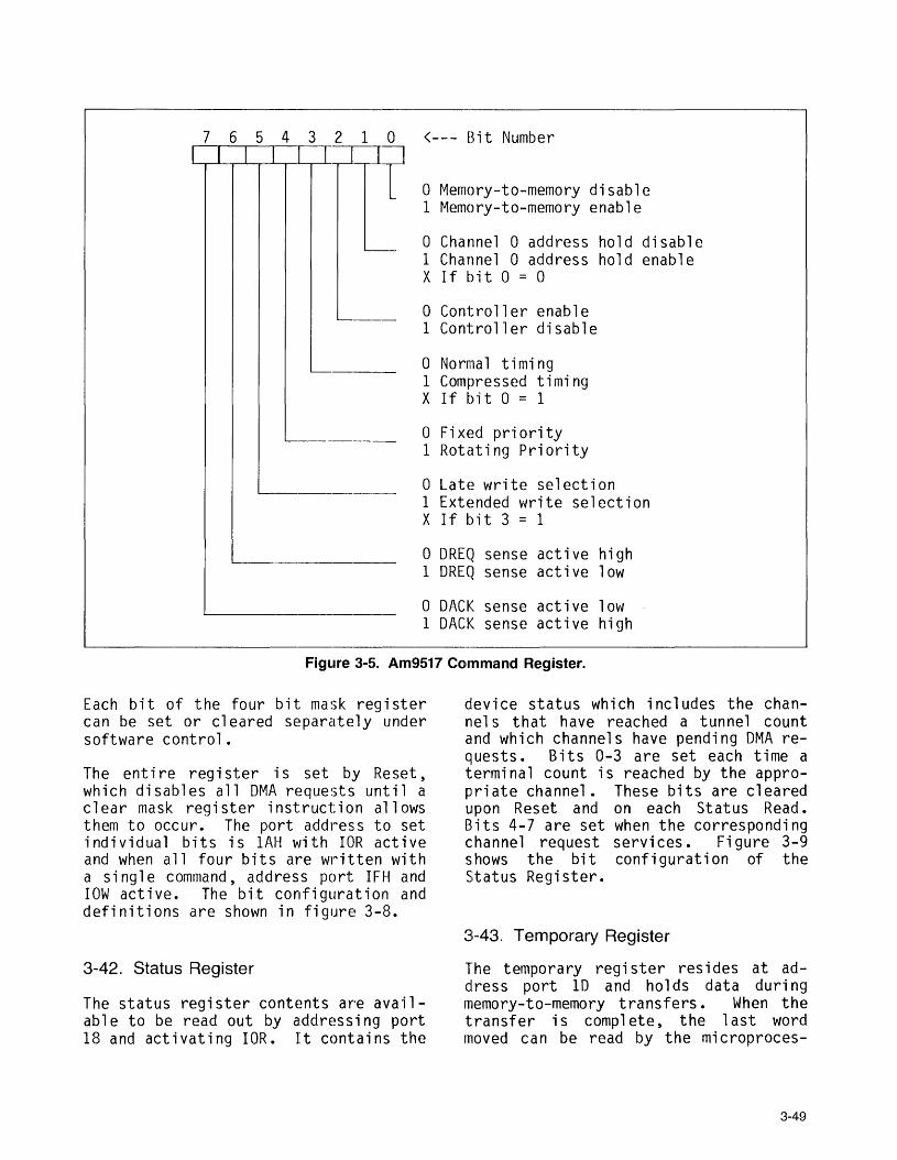
,....---------------_._-----
<--- Bit Number
o Channel 0 address hold disable1 Channel 0 address hold enableX If bit 0 = 0
o Controller enable1 Controller disable
o Late write selection1 Extended write selectionX If bit 3 = 1
o Memory-to-memory disable1 Memory-to-memory enable
o DREQ sense active high1 DREQ sense active low
o Fixed priority1 Rotating Priority
o Normal timing1 Compressed timingX If bit 0 = 1
1 0
T5 4 3 267
I I I I I I I I
-
'-----
---
1--_----_._-
'-----------
o DACK sense active low1 DACK sense active high
'-------------------------------------------'
Figure 3-5. Am9517 Command Register.
Each bit of the four bit mask registercan be set or cleared separately undersoftware control.
The ent ire reg i ster is set by Reset,which disables all DMA requests until aclear mask register instruction allowsthem to occur. The port address to setindividual bits is lAH with lOR activeand when all four bits are written witha single command, address port IFH andlOW act i ve. The bi t confi gurat i on anddefinitions are shown in figure 3-8.
device status which includes the channe1s that have reached a tunnel countand which channels have pending DMA requests. Bits 0-3 are set each time aterminal count is reached by the appropriate channel. These bits are clearedupon Reset and on each Status Read.Bits 4-7 are set when the correspondingchannel request servi ces • Fi gure 3-9shows the bit configuration of theStatus Register.
3-42. Status Register
The status register contents are available to be read out by addressing port18 and activating lOR. It contains the
3-43. Temporary Register
The temporary regi ster res ides at address port 10 and holds data duringmemory-to-memory transfers. When thetransfer is complete, the last wordmoved can be read by the mi croproces-
3-49

00 Channel 0 select01 Channel 1 select10 Channel 2 select11 Channel 3 select
00 Verify transfer01 Write transfer10 Read transfer11 IllegalXX If bits 6 and 7 = 11
o Autoinitialize disable1 Autoinitialize enable
o Address increment select------1 Address decrement select
00 Demand mode select01 Single mode select10 Block mode select11 Cascade mode select
Figure 3-6. Am9517 Mode Register Bit Assignments.
---._-_._-_._------------------
Don't Care
7 6 543 2 1 0co:==rr°-r---r-._rJ-[
<--- Bit Number
00 Select channel 001 Select channel 110 Select channel 211 Select channel 3
o Reset request bit1 Set request bit
3··50
IFigure 3-7. Am9517 Request Register.

SET/RESET
7 6 543 2o=r=III
Don't Care
4-bit MASK
1 0TI
L<--- Bit Number
00 Select channel 0 mask bit01 Select channel 1 mask bit10 Select channel 2 mask bit11 Select channel 3 mask bit
0 Clear mask bit1 Set mask bit
7 6 5 4o=r=I
Don't Care
<-_ .. Bit Number
0 Clear Channel o mask bit1 Set Channel 0 mask bit
0 Clear Channel 1 mask bit1 Set Channel 1 mask bit
0 Clear Channel 2 mask bit1 Set Channel 2 mask bit
0 Clear Channel 3 mask bit1 Set Channel 3 mask bit
Figull'e 3·8. Am9517 Mask Register.
sore This register always contains the1ast byte transferred in the previ ousmemory-to-memory operation, unlesscleared by a Reset.
3-44. SOFTWARE COMMANDS
There are two additional software commands that can be executed on theAm9517 that do not depend on any specific bit pattern on the data bus. Thesetwo commands are described in the following paragraphs and the address codesare shown in table 3-6.
3-45. Clear First/Last Flip/Flop
This command is executed prior to writing or reading new address or wordcount information to the Am9517. Thisinitializes the flip/flop to a knownstate so that subsequent accesses toregister contents by the microprocessorwill address upper and lower bytes inthe correct sequence.
3-46. Master Clear
This software instruction has the sameeffect as the hardware Reset. TheCommand, Status, Request, Temporary,
3-51

_._._----_..-.--_._-----_._--------------
7 6 5 4 3 2 1I I I I -' I I I
-
L...______
-----
a <--- Bit Number
L1 Channel a has reached TC1 Channel 1 has reached TC1 Channel 2 has reached TC1 Channel 3 has reached TC
1 Channel a request1 Channel 1 request1 Channel 2 request1 Channel 3 request
Figure 3-9. Am9517 Status Register Configuration.
TABLE 3-6. SOFTWARE COMMAND CODES.
Operat ion RegistersAffected
SignalsCS lOR lOW A3 A2 Al AO
Clear FF
MasterClear
InternalFirst/LastFl i p/Fl op
Clear:CommandStatusRequestTemporaryInterna1First/LastFl i p/Fl opSet: Mask
a
o
1
1
a 1 100
o 1 101
and Internal First/Last Flip/Flopregisters are cleared and the Maskregister is set. The Am9517 will enterthe Idle cycle.
3,·47. FLOPPY DISK FORMJ~TTER/
CONTROLLER FD177"'
The FDI77I is a MaS/LSI device thatperforms the functions of a floppy diskcontroller/formatter. The device isincluded in the floppy disk controllerboard, and contains a flexible interface organization that accomodates thefirmware interface and the disk driveinterface.
3-52
The firmware/processor interface consists of an 8-bit bidirectional bus fordata, status, and control word transfers. The device operates on a multiplexed bus with other bus-orienteddevices.
3-48. PROCESSOR INTERFACE
The FDI77I to Am9085 processorinterface is accompl i shed through theeight Data Access Lines (DAL) andassociated control signals. Data,status, and control words out of orinto the FOI77I use the OAL. The DALcontains three state buffers, which are

enabled as output drivers when ChipSelect and Read Enable are active, andenabled as input receivers when ChipSelect and Write Enable are active.
When data transfer through the F01771is requ i red by the Am9085 , the dev iceaddress is decoded making the ChipSelect (CS) line active. The fouraddress parts on the FOI77'1 and theaccessed registers are listed in table3-6. The least significant addressbits A0 and Al are coded to select theregisters listed.
Ouri ng DMA types of transfers betweenthe F01771 Data Register and the bufferor main memory, the Data. Request (ORQ)output is used in Data Transfer Control. This signal also appears asstatus bit 1 during read and writeoperat ions.
3-49. FLOPPY DISK INTEHFACE
The floppy disk interface consists ofhead positioning controls, wr"ite gatecontrols, and data transfer lines. A2.0MHz +1% squarewave clock is requiredat the elK input for internal controlt imi ng. Commands read into the FOI77Ifrom the Am9085 are implemented and theappropriate signals are sent to aselected disk drive.
3-50. COMMAND DESCRIPTIC)N
The FOI771 accepts and executes elevencommands. The command words should beloaded into the command register onlywhen the busy status bit is off (StatusBit 0). An exception is the ForceInterupt corrnnand. When a command isbeing executed, the busy status bit isset. When a command is compl eted, aninterrupt is generated and the BusyStatus bit is reset. The statusregister indicates whether a command iscomputed or an error occured. Thecommands are divided into four typesand are explained in the followingparagraphs.
3-51. Restore (Seek Track 0)
When this command is read into the command register and execution is implemented, the track 00 (TROO) input issampled. If TROO is active, indicatingthe Read/Write head is positioned overtrack 0, the track register is filledwith zeroes and an interrupt is generated. If TROO is not active, steppingpulses, at a rate specified by bits 0and 1, are sent to the drive unit untilTROO is activated. At this time the TRis filled with zeroes and an interruptis generated. 1fthe TROO does notactivate after 255 stepping pulses, theoperation is terminated automatically,the interrupt is set, and the seek error status bit is set. A verification operation occurs if bit 2 of thecommand is set. The Restore command isimpl emented automatically when themaster reset occurs. Fi gure 3-10 i 1lustrates the bit configuration of thecommand register for a RESTORE corrnnand.
3-52. SEEK
This command assumes the track registercontains the current Read/Write headtrack position and the data registercontains the desired track number. TheFOI771 updates the track regi ster andissues stepping pulses in the properdirection, positioning the Read/Writehead, unt il the contents of the trackregister equal the data register. Atthis point the Read/Write head is positioned over the desired track. Aninterrupt is generated at the end ofthis operation. Figure 3-11 illustra.tes the command register bit configuration for a SEEK command.
3-53. STEP
Upon receipt of this command, theFOI77I issues one stepping pulse to thedisk drive. The stepping motor direction is determined by a previously issued STEP IN or STEP OUT command. An
3-53

1 - Verify on last tracko - No verify
__________ 1 - Head load at beginningo - Do not load head at beginning
'-----------
<--- Bit Number
00 - 6ms01 - 6ms Stepping Rates10 - 10ms11 - 20ms
RESTORE
Fi!Jure 3-10. FD1771 RESTORE Command.
SEEK
<--- Bit Number
o - No verify1 - Verify on last track
o - Do not load head at beginning1 - Load'head at beginning
SteppingRates
00 - 6ms01 - 6ms10 - 10ms11 - 20ms
'----------
IFigure 3-11. FD1771 SEEK Command.
interrupt is generated at the compl etion of this command. Fi~Jure 3-12 illustrates the command register bit configuration for a STEP command.
coomand. Figure 3-13 illustrates thecorrrnand register bit configurat~ion fora STEP-IN command.
3-55. STEP-OUT
3·-54. STEP-IN
The STEP-IN command causes the F01771to issue one stepping pulse such thatthe Read/Write head moves one track toward track 76. An linterrupt isgenerated at the completion of this
The STEP-OUT command causes the F01771to issue one steppi ng pul se such thatthe Read/Write head moves one tracktoward track O. An interrupt isgenerated at the completion of thiscommand. Figure 3-14 illustrates thecommand register bit configuration fora STEP-OUT command.
3-54

..-------------------------------------------,
(--- Bli t Number
00 - 6ms01 - 6ms Stepping Rates10 - 10ms11 - 20ms
____ 0 - No veri fy1 - Verify on last track
o - Do not load head at beginning1 - Load head at beginning
o1
No update- Update track register
STEP
Figure 3-12. FD1771 STEP Command.
..---------------------------------------~
(--- Bit Number
00 - 6ms01 - 6ms Stepping Rates10 - 10ms11 - 20ms
o - No verify1 - Verify on last track
o - Do not load head at beginning1 - Load head at beginning
o - No update1 - Update track register
STEP-IN
Figure 3-13. FD1771 STEP-IN Command.
3-56. READ
When the READ command is issued to theFD1771, the following events occur~ TheRead/Write head is loaded, the Busystatus bit is set; and when the 10field (with the correct track number,sector number, and CRC) is encountered,the data read from the disk data field
is transferred to the DMA controllerfor routing. The Data Address Mark (AM)must be found wi thi n 28 bytes of thecorrect fi e1d; if not, t he Record NotFound status bit is set and the operat 'j on is termi nated. When the fi rstcharacter or byte of data is shi ftedthrough the Data Shift Register (DSR),it is transferred to the Data Register
3-55

(DR) and DRQ is generated. When thenE~xt byte is encountered in the DataShift Register (DSR) , it is transferredto the DR and another DRQ is generated.If the DMA has not read the previouscontents of the DR before a new character is trans ferred, that character islost and the Last Data status bi tisset. Thi s sequence is repeated unt i 1the entire data field is read. If aCRC error occurs at the end of the data
field, the CRC error Status bit is setand the command is terminated.
When the read 0 perat ion i s com p1et e ,the type of Data Address Mark read inthe data field is recorded in theStatus Register. For a definition ofthe bits affected, see the StatusRegister description. FiguY'e 3-15illustrates the command regi ster bitconfiguration for a READ command.
-------_._------_._-----------------
7 6 5 4 3 2 1 01011111XIXIXIXill
L
1-- _
<--- Bit Number
00 - 6ms01 - 6ms Stepping Rates10 - 10ms11 - 20ms
o - No verify1 - Verify on last track
o - Do not load head at beginning1 - Load head at beginning
o - No update1 - Update track register
STEP-OUT
Figure 3-14. FD1771 STEP-OUT Command.
1 = HLD set active and HLD is sampledafter 10ms delay
0 = NON-IBM format (128 to 4096 bytes)1 = IBM format (128 to 1024 bytes)
0 - Single record1 -- Multiple redord
Read command
'-------
1-- _
2 1 0 <--- Bit Number..-----r.--,---,----r----r--1ill]]
Figure 3-15. FD1771 READ Command.
3-56

3-57. WRITE
Upon receipt of the WRITE command, theRead/Write head is loaded (HLD active)and the Busy status bit is set. Whenthe correct 10 field is located, a DRQis generated. After 11 bytes of theCRC field, Write Gate (WG) activates ifthe DRQ is serviced. If the Data Regi ster has not been loaded, the corrmandis termi nated and the Lost Data statusbit is set. If the DRQ has bE~en servic ed, WG act i vatesand six byt es 0 fzeroes are written on the diskette.
The FD1771 proceeds to wri te the datafield and generate DREQ to the DMA. Ifa Data request is not serviced in timefor continuous writing, the Lost DataStatus bit is set and a byte of zerosi s wr ittenon the dis ket t e , but thecommand is not terminated. When thelast data byte is written, the two-byteCRC is computed internally and written,followed by a one byte gap of logicones. The command is then tenni nated.Figure 3-16 illustrates the commandregister bit configuration for a WRITEcommand.
3··58. Read Address
When the Read Address command is i ssued, the read/write head is loaded andthe Busy status bit set. The first 10field encountered is read and the sixdata bytes in this field are assembledand transferred to the data register.A DRQ is generated for each byte. TheID address field is shown in figure3-·17.
The FD1771 checks for validity and setsthe CRC error status bit when a CRC error is detected. The sector address ofthe 10 field is written into the sectorrE~gister. When the operation is compl ete, an interrupt is generated andthe Busy status bit reset. Figure 3-18illustrates the command register bitconfi gurat i on for a READ ADDRESS command.
3-59. Read Track
The Read Track command is impl ementedin the same manner as the Read Addresscommand except the Read Enable signal
7 6 5 4 3 2 1 0 <--- Bit NumberI 1 I 0 I 1 I XI XI lTIDJ
-[~DATA CLOCK
AM(HEX) AM(HEX)00 - FB C7 ADDRESS01 - FA C7 MARK10 - F9 C7 DETERMINATION11 - F8 C7 FIELD
1 = HLD Set active and HLD is sampledafter 10ms delay
'-------
'-------------
o = Non IBM format (16-4096 bytes)1 = IBM format (128-1024 bytes)
o = Single record1 = Multiple record
WRITE COMMAND
1-- . ----1
Figure 3-16. FD1771 WRITE Command.
3-57
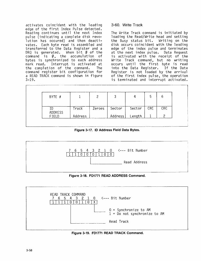
activates coincident with the leadingedge of the first Index Pulse detected.Read i ng cont i nues unt i 1 t he next Indexpulse (indicating a complete disk revolution has occured) and then deact"ivates. Each byte read is assembled andtransferred to the Data Register and aDRQ is generated. When bi t 0 of thecorrrnand is 0, the accumulation ofbytes is synchroni zed to each addressmark read. Interrupt is act i vated atthe completion of the command. Thecommand regi ster bi t confi gurat i on fora READ TRACK command is shown in figure3-19.
3-60. Write Track
The Write Track command is initiated byloading the Read/Write head and settingthe Busy status bit. Writin~1 on thedisk occurs coincident with the leadingedge of the index pulse and terminatesat t he next index pul se. Data Requestis act i vated wi th the recei pt of theWrite Track command, but no writingoccurs until the first byte is readinto the Data Register. If the DataRegister is not loaded by the arrivalof the first index pulse, the operationis termi nated and interrupt act i vated.
------------------------------------------ ----,
BYTE #
10ADDRESSFIELD
1 2
Tr~ack Zeroes
3 4 5 6
Sector Sector CRC CRC
Address Length 1 2
Figure 3-17. 10 Address Field Data Bytes.
7 6 5 4 3 2 1 0 <--- Bit Number[JJJJ 0 [[I[I~IIQIQ]
~. Read Address
Figulre 3-18. FD1771 READ ADDRESS Command.
---------------------------- ----I
READ TRACK COMMAND7 6 5 4 3 2 1 0 <--- Bit Number
ITIIIIITIQITCQ=r+J
L ~--- 0 = Synchronize to AM1 = Do not synchronize to AM
Read Track--_..._--~-~-
Figure 3-19. FD1771 READ TRACK Command.
~~-58
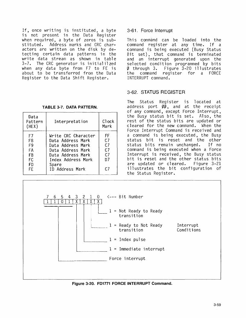
If, once writing is instituted, a byteis not present in the Data Registerwhen required, a byte of zeros is subst i tuted. Address marks and CRC characters are written on the disk by detect i ng certa in data patter'ns in thewri te data stream as shown in table3-7. The CRC generator is initialilzedwhen any data byte from F7 to FE isabout to be transferred from the DataRegister to the Data Shift Register.
TABLE 3-7. DATA PATTERN.
DataPattern Interpretat oj on Clock(HEX) Mark
F7 Write CRC Character FFF8 Data Address Mark C7F9 Data Address Mark C7FA Data Address Mark C7FB Data Address Mark C7FC I ndex Address Mark 07FD SpareFE ID Address Mark C7
L-- ~ . __'
~~-61. Force Interrupt
Th i s command can be loaded into thecommand register at any time. If acommand is bei ng executed (Busy StatusBit set), that command is tenninatedand an interrupt generated upon theselected condition programmed by bits~ through 3. Figure 3-20 illustratesthe cOlTll1and regi ster for a FORCEINTERRUPT command.
~1-62. STATUS REGISTER
The Status Regi ster is located ataddress port 0~, and at the recei ptof any command, except Force Interrupt,the Busy status bit is set. Also, therest of the status bits are updated orcleared for the new command. When theForce Interrupt Command is received anda command is being executed, the Busystatus bit is reset and the otherstatusb its r emai nunchanged • If nocorrrnand is bei ng executed when a ForceInterrupt is received, the Busy statusbit is reset and the other status bitsare updated or cleared. Figure 3-21illustrates the bit configuration ofthe Status Register.
1 0 <--- Bit Number....---:--T----::--r--::--r--:---r-:-:-r--:~)P=P_ 1
~ Not Ready to Readytransition
IL__ 1 Ready to Not Readytransition
___ 1 = Index pul se
InterruptConditions
1 Immediate interrupt
'---- , Force interrupt
Figure 3-20. FD1771 FORCE INTERRUPT Command.
3-59

---_..._--_.._------_._--------------------,
ek
Y
OTECT
JLT
A
Read WritTrack Write Trac
NOT READY NOT READY NOT READ
0 WRITE PROTECT WRITE PR
0 WRITE FAULT WRITE FAI
0 RECORD NOT 0FOUND
0 CRC ERROR 0
LOST DATA LOST DATA LOST DAT
DRO DRO DRO
BUSY BUSY BUSY
Read
NOT READY
RECORD TYPE
RECORD TYPE
RECORD NOTFOUND
CRC ERROR
LOST DATA
DRO
BUSY
All Type I ReadBit Commands Addre,ss
S7 NOT READY NOT REJlDY
S6 WRITE PROTECT 0
S5 HEAD ENGAGED 0
S4 SEEK ERROR ID NOTFOUND
S3 eRC ERROR CRC ERF~OR
S2 TRACK 0 LOST DATA
S1 INDEX DRO
AO BUSY BUSY--_.--'-.
-----------_ .._----_._---_._._-------_....•...._---------------
FIGURE 3-21. FD1771 Status Register.
3-60

CHAPTER 4THEORY OF OPERATION
4.1 GENERAL INFORMATION
The FDC board accepts commands andparameters from the host system,interprets the commands and producescontrol signals to iinit"iate oprationsi nthe LSI c i rc uits (FD1771A Flo PPYDisk Formatter/Controller anel Am9517Multimode DMA Controller), outputsope rat i ng s i gna1s tothe dis k un its ,interfaces di sk data between the di skunits and FD1771, and inputs statusinformation from the disk units.
The functions to format disk data,transfer data between the FOC board anddisk units, control disk unitoperations, and transfer data betweenthe FDC and Host memory are performedby the DMA controller. Functionaldescriptions of these operat"jons arenot inc1uded herei n. Refer to theappropriate data sheets. (Seereferences at the front of thismanual).
All operations are under control of theon-board CPU and firmware. A blockdiagram of the Am95/6110 FOC board isshown in figure 4-1.
4-2. INSTRUCTION EXECUTION
Operations on the FOC board are theresul t of recogni zi ng the command andimplementing on-board firmwareroutines. One command is described indetail. The remaining commands areexecuted ina simil ar manner and thedetailed descriptions are not included.
4-3. READ A SECTOR OPIERATION
The host CPU send s t he page segmentparameter to RO, the MSB of the dataaddress (in master memory) to Rl, and
the LSB of the data address to R2. Thecommand and sector count is then sentto R3.
The receipt of data into R3 causes theCOMMAND-IN flip-flop (U7) to set. Thestatus regi ster is cl eared; the boardis in busy state. When in its idlestate, the on-board CPU polls the stateof this flip-flop. When the flip-flopsets, the on-board CPU inputs thecommand from R3 and determines therequired operation.
In this case, a READ operation isfound. The data in RO, Rl, and R2 areretrieved and used to set-up the DMAcontroller. The DMA controller can beset to transfer either single bytes orblocks of 128 bytes for each DMArequest. For thi s exampl e, the DMAcontroller is set for single-byte DMA.
The on-board CPU then loads the track,sector, and command into the FD1771controller. Unit, track, and sectorparameters are sent from t he host CPUduring a previous SETPAR command.
When the sector is reached and a bytei s ass embled, the DR EQ s i gnali sraised. This is converted into the DMAREQUEST signal for the Am9517 DMAcontroller. The Am9517 sends an HREQto the on-board CPU and a bus requestis sent to the host system. When themaster bus is obtained, the DMAcontroller generates a DMA acknowledge.This signal is also the chip selectsignal for the FD1771. The byte ofdata is transferred to main memory.When the byte is transferred, the DREQsignal is dropped and the Am9517controller releases the CPU from HOLD.
Following transfer of the whole sector,the FD1771 generates an INTRQ to theon-board CPU. The on-board CPU is
4-1

interrupted and it then retrieves thedri ve status i nformat i on from theFOI77I and places this infonnation inmail-box register R4. Also, bit-7 ofR4 'j s sent to s i gni fy that the
controller is no longer busy. If bit-6of the previous Unit Code received wasset, an interrupt request is sent tothe host system. The on-board CPUreturns to the Idle State.
--_._--------------_._---------------------- ------_.
P4
[:::J
P4
I---+---[:::JDRIVESEL.
BUFFER P4
--[>-[:::J
FLOPPYDISK
CONTROLLERFDl771
P3
r----------[:::J
RAMIE-PROMAm9114/Am2708
f--- ------~
16
ON-BOARDCPU
Am9085
P3
.-------------~----------------------CJ
[
DMA ]Am9517
'-
MAILBOXREG.
8-BITADDER
DATD-DATF
FIGURE 4-1. Floppy Disk Controller Functional Block Diagram(Control Signals are not Shown).
4-2

CHAPTER 5SERVICE INFORMATION
5-1. INTRODUCTION
This chapter provides infonnation onservice and repair assistance, userreplacement parts and service diagramsfor the AMC 95/6110 Single DensityFloppy Disk Controller.
5-2. SERVICE AND RIEPA!IRASSISTANCE
If it is necessary to Y'eturn the AMC915/6110 Floppy Disk Contr'oller boardto Advanced Micro Computers for serviceor repair, contact the Service Managerfor OEM Products at the telephonenumber listed below. A Return MaterialAuthorization number must be obtainedprior to shipment. When the reshipmentis due to the board being damagedduring shipment from AMC, or the boardis out of warranty, a purchase order isrequired to complete the repair.
Repackage the board in the originalpacking material or an equivalentsubstitute, and enclose in a corrugatedcarton suitable for shipping. Seal theshipping carton securely, mark itFRAGILE, and address to:
Advanced Micro ComputersService Manager, OEM Products3340 Scott BoulevardSanta Clara, California 95051
TELEPHONE: (408) 988-7777
TOLL FREE:800-672-3548 California800-538-9791 U.S.A. (except
California)
5-3. USER REPLACEABLE PARTS
Listings of all user replaceable partsis provided in table 5-1. Figure 5-1is the component location diagram.
5-4. SERVICE DIAGRAMS
The Floppy Disk Controller componentlocations are shown on the assemblydrawi ng, fi gure 5-1. Part numbers forthe components shown on the assemblydrawing are listed in table 5-1.
Schematic diagrams of the Floppy DiskController are shown in figures 5-2through 5-6. Active-low (logical ~
signals are specified by an asterisk(*) following the signal name.
5-1

AMC PartNumber
TABLE 5-1. USER REPLACEABLE PARTS.
Description Location
2000322000812000182'000842'000452000042000012'000032:100082'000212'200272:000572'200222'200172000522'000752'800062'000782~10007
2~00016
2'600282'000802~60009
2'000202~30012
2~800 112000852~20005
2000822600142000832:000412~00042
2~00035
2~20016
2~20002
450019450021690022340011340002340047310002630029630017630033630065630063
Integrated circuit, Type 74LS04Integrated circuit, Type 74LS164Integrated circuit, Type 74LS244Integrated circuit, Type 74LS109Integrated circuit, Type 74LSOOIntegrated circuit, Type 74LS74Integrated circuit, Type 74LS08Integrated circuit, Type 74LS32Integrated circuit, Type 7407Integrated circuit, Type 74LS253Integrated circuit, Type 74S257Integrated circuit, Type 74LS11Integrated circuit, Type 74S05Integrated circuit, Type 74S04Integrated circuit, Type 74LS138Integrated circuit, Type 74LS373Integrated circuit, Type 8304Integrated circuit, Type 74LS273Integrated circuit, Type 7483AIntegrated circuit, Type 74LS240Integrated circuit, Type 8085Integrated circuit, Type 74LS260Integrated circuit, Type 9517Integrated circuit, Type 25LS2521Integrated circuit, Type 9114EIntegrated circuit, Type 8303Integrated circuit, Type 25LS2518Integrated circuit, Type 74S139Integrated circuit, Type 74LS670Integrated circuit, Type FD1771Integrated circuit, Type 74LS123Integrated circuit, Type 25LS2520Integrated circuit, Type 74LS193Integrated circuit, Type 74LS163Integrated circuit, Type 74S240Integrated circuit, Type 74S0024 Pin I.C. Socket40 Pin I.C. SocketSwitch, Recess Rocker, 6 POSeCapacitor, Ceramic .1~f, 50V, 20%Capacitor, Tantalum, 22~f, 15V, 20%Capacitor, Tantalum, 4.7~f, 16V, 20%Diode, IN914Resistor, Carbon, 1K, 1j4W, 5%Resistor, Carbon, 4.7K, 1j4W, 5%Resistor, Carbon, 10K, 1j4W, 5%Resistor, Carbon, 27K, 1j4W, 5%Resistor, Carbon, 47K, 1j4W,1 5%
U1, 10, 62U2, 5U3, 27, 34U4U6U7, 13,38, 39, 44, 68U8, 17, 61U9, 18, 19, 55, 64U12, 63U14, 15U16U20U21U22U23, 24, 45U25, 35U26U28, 29U30, 36U31, 37, 41U32U33U40U42U49, 50U51, 52, 58, 67U53U54U56, 57U60U65U66U69U70U59U11U46, 47, 48U32, 40, 60U43C2, 3, 4
C25, 26CR1, CR2R1, 6, 7 14R2, 3, 4, 10, 11R5, 8, 9, 15R12R13
5-2
__._. .. ._. ._. . --1.- _

AMC PartNumber
TAElLE 5-1. USER REPLACEABLE PARTS (Cont.).
Description Location
630014630057630056630500630508480011
Resistor, Network, 4.7K, 8 POSe RPl, 4, 5Resistor, Network, 4.7K, 6 POSe RP2Res i stor, Network, 4. 7K , 10 POSe RP3, 6, 7Resistor, Network, 10K, 6 Pos. RP9Resistor, Network, lK, 6 POSe RP88MHz Clock, OSC Yl
5-3

Figure 5-1. Am95/6110 Components Location.

o
c
B
A7 A2AI A6A5MMA9A3~C5U50
9114
I. CI,C5-C20, C23,C24, C27-C32 ARE .I ..d'DECOUPUNG CAPACITORS. (2ll" PLACES).
NOTES:
INH.
5 ~ 4
U54IY3 7
IY2 165139
'YI-~
67
101M 34
U32
8¢85
vee
I
....£ X2.
+svR7IK
CPCLK
eLK
8
73 c:-JRST 5.5
71 ~ TRAP
g-ro198~ INTR
r 97
HOS5~ HOLD
~~978 4AIS 28 2 IAI IYI 18 IAOFAI4 27 17 2A4 Z'f.'IJ-"3'--4-+-Ir---------+-----------+------------+---+---- IADEAI3 I ~'" II 2A1 U34 ZYI 9 IADDAIZ 25 8 IA4 LS IY,," 12 IADeAll 24 4 1A2 244 IY2 16 IADBAll!! 23 '15 ZA3 2Y3 '5 rADAAS 22 6 IA::! IY31l140!---h-------I'------r------+---~-------+-_+-4----------~r--------- IAD9
A8t2QI--------l.>13~I~G)~«"~)2~Y~2~7~:_-Hi------i---tr-----t---tr------t-l-li----------tl-------IA08
,...------+-40>1 U25 y>lJ=2=----H-+-t---------.;Ie-----+h-----+---+-+..,.......-----t-------Ir--+-+-1--------+-+~----- IAD7r--------t....I,,4 0S LS Y5
15 'T T J T IADG
I 8 03 Y3 9 I lAOS
I13 D4 373 Y4 12 J I I I T IA04I I IS 07 Y7 19, I I I 1 I I T I I T I I T I I ! IA03
11111111~'------~'. ~-~ Wfififfi=::~;ALEI~'II'11j
11,1 L:-----11 I +~"~H+,,~1Z2-+-1.1231H-!U+-+J4--H.isl-+,U+-+sL-o--------'-hJ+-+'JZ-+-3
1,t-+1.213+-+1415-+-16+-+17 lal+-''20-119!"lJ 121~ 14 U, 17 U20 Ii7U611 I~ 1~13l51JJe
A9 A8A7 A6ASA4A3 AlAI A~ es A9 A8A7 A6A5A4A3 AlAI A~ C5 A9A8A7 AGA5A4A3 AlAI A/ll CS A7A2AI A6 ASAllMA9A3A0CSALE, U47 U46 U48 U49
I I III' II 1'1 IIIMEM
2
R
9
" 24 PIN PROM SOCKET 24 PIN PROM SOCKET 24 PIN PROM SOCKET 9114
Q7Q ;Q5Q"HQ2QI Qtl C7 Q4iQ5t Q3Q2QI Gil Q7 (5C 5C4CI3Q2QI :HI RIW C I 2 C3 Q4 RIW Q 1 Q4 Q3 (2
IS 21 17 i'6 15 ~ 13 " I~ 9 lis 121 17116 15 14 13" W 9 118l' 17 16 IS 14 13 II ID 9 I'" 14 13 12 II I'" 14 II 12 13
II 'I I "-1"'30~'-+--++++++H-_------41....,.1++'++++t-+--~I j I/" 1 I IMEMW. --<>--+--+---+_--+- -.-J
II I ~'::~ ". ,,~o I I,AD"! pI9........+-+-+-+-+-l_+__---""!2 AI R I J!1"'s-+---......:.:::......>-++-H-+-Hi-----........H-+-+-I-+--+--------<4-+-+-I-++-+-------+----1I--+----+------_+__----1---+---+--- IOB7A06 '8 II "AA. 64 15 i IOB6ADS 17 8 A7 U26 87 12 lOBSA04 16 I 7 A6 a3~4 86 13 I IOB4-A03 15 I A~ 8~ lSi 1083ADZ 14 4 A3 83 16 1082ADI 13 3 A2 82. 17. IOBI
AO¢ 12 6 AS V"R C5 B5" +SV IOB~
r-t7:s::;-v--I-s---,11~ .[IDJU
RPI
l--§3 IA 3578 4.7KViR 31 18W 2A U16 IY ",4-'--:-~-"F'-f--F--- now <Ii
TOTAL 36 -- ThiTA~'2 ------,.§ 2B 2Y 7RESET.---= ~~5ET I UI7 3 o------l14AS257 i IMEMW.
74¢7 _ LSIll~ ~ 48 4Yp.:=12+---......t+---IIOR It
85~ SOD RO :~ 3A 3Yt:>"-9--t----t+---IMEMR.
86,tf SID ------:.::.3B OE~ ~MERW*RIO 38 i HACK~
",/..1~ 5V 4,7K HLOA~(II4S!2I4I'< fl'~ RES~[~UT 3 II UI 10 9 UI 8 RST
84 37 RST.
4 U3 16 eLK
COM''''
URINT
Sf'S
~TMCT
IINTREQ i 8a 87 7 RST7.S
EOPINT -1?0 ~ RST6.5
o
B
c
-
LS24-'"
AUNLESS OTHERWISE SPECFlEDDlIlENSlONS ARE IN INCHESTOlERANCESAAE
r----,--------lFRACTKlNS DEClIU.LS ANGlES A
<n '3:="~8
cJ,7 6 5
THIS _ CONTAINS 1NFORII.vKlIlWHICH IS THE PROPRETARY ..-ERTYOF ADYAJICED IIICRO COIlPUTERS INCORPORATED. THIS DRAWING ISRECEIVED IN CONFIOENCE AND ITSCONTENTS IIAY NOT 11£ DISCLOSEDWITHOUT THE PRIOR WRITTEN CONSENTOFAIIC 1IlC.
4 3 2
SCHE.MATIC DIAGRA M
FLOPPY DISK C.ONTROL
Figure 5-2. Am95/6110 Schematic Sheet 1.
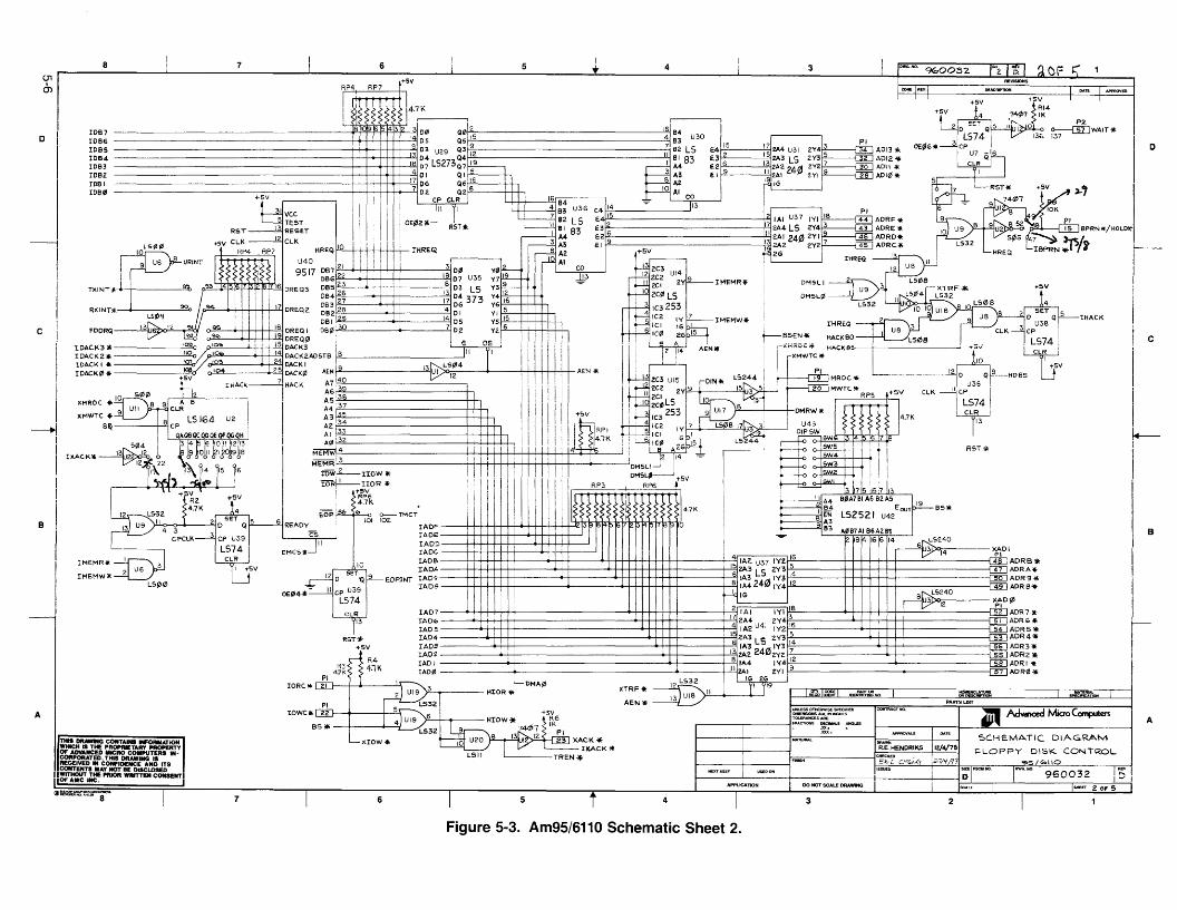
o
B
A
IHACK
+SV
SCHEMA.TIC DIAGRAM
l=OLOPPY DISK. CON.TROL~S/IDI\O
+S.V +f: .744>7+!~~4~_ "._~ P2.
LZ.j0 -_. QM~ ~WAIH
~ LS74 I ~ 136 137
0E¢6¥ 3~CPU7 Q 6
CL.RI
SI7 L-RSTlIE
74rtJ79 I 8
52 PI15 8PRNlI'/HOL.0lC'
"'~).,t:,/,16PRN.l",J' I
I
II c
I
LII
I
CHECKED •
EX, C (}I&Ak ;;"7/~/79
23
E4 IS
E31-"'------'-"1E,2 ""6-----''''1E I p'S'--__'-'-I
UHlESSOTHEFlWlSESPECIFlB:lOUENSIONSAAEIN RilCHESTOLERANCES ARe:
.----- ,--__~Ff\&.CTlOHS DECIMALS
45
1~---------------_____l.'2j16i84f-l:'C-------------------:ti4163 U30P,;;------------------,Li7 82 L5~-----------------!.ljl: :~83
3 A38 A2HAl
-=- ~""':CT-~3=------'
6
CL.R13
RSTil'
nsv
R4~~ 4.1K
-sf-P-12 0 'Q~EOPINT
CP U3S
L574
IOWC.
PIlORe.. 21
OMC5.
C4 14
IE. IS AORF lIIiE3i"'----------------j!.!.j r-----, , I AORE 11'<
E.2:f"6'--------------+'-4 r---, , ,AOROll<HREQ ~IO"--'H-+-+-+-l--l-l-- JHR~Q IE. I p'9'-- ~ r--.., .." ,AORC.~
U40 21 I ! i : I I 3 0'" y",l~ ,.JJ.!I AI co r~,v.-----_ IHRfQ I II9517 DB7 ., .,"'-- , I ~ 2C3 I 12 us
086;23
I :: I~ 07 U3S Y7k-g9
:g3 ~2C2 UI:Y~IMEMR* DMSll lS08DBS 03 L5 Y3""-- o----u 2CI I US 3 ~GXTRF"*DB4 26 1 13 04 Y40£-- ~ 2C¢ LS I DMSL.¢ 1 ~LS¢4 LS32DB327 I 17 06 373 Y6i-!'16~-I-+-+-h '~IIL1"-l508DB2i"'2£8---.......,'-+----....:!.J4 01 YI !-"S'---l--+--I---+-l-. ~ 1C3253 I L53 1/"'10 10 UIB 810OBI I~'l 14 OS Y5 IS i ""5 IC2 IV l--IMEMW" U8 8
30 6 Il >---", ICI 16 ~I IHREQ 2 9OB¢ i 7 02 Y2. :" 6!21 IS' I US 3 ClK
'I 111l r--" IC 26 t---BSEN'll; HACK 80 '-----'" L508
f.Si~-------,,;rr ii",. ii, i:, ii, I' i',I; I' AENlI'< l ~I"1>14'. AENiIl II ;(;.":~~;C. HACKes I 12~9:;1;, ~ ,-"","" """ ",.. :i ""CO "------------I'",,'r-
:~~ ~ ;,;,:: I': l~ZCZ 9 i IS~:'~ ~MWTCli< U3B
gl:~ IIIII i I ~iZ~i~:'1 ~,1%= ! ~'W'I RP5 +5( elK II C;~~4 I
:~:f"3",,-3---_----------j' 1I11IIII ~'" :d:~;" ~ ""'~~ ,,~~;. I'" "AIll!32 iii Ii i 11 ! Iii iii IJt-lt·,K i '---.2.jIC!2I ~G 1S t L5244 SW6 4 "'78
=~I,-,,;;~:::::::::::::::::::::::::::::::::::::::::::::::::::::::::::::::::::::::::::::::::t~i~~!:~'ttti~~I::::~tttit~I~:=~I~::::::::::::~I---! ~2 AI~G ~ ,.-------' EE ~:~ I i Rsa! lTl 1 l1T II I OMSll-' SW3 i I I
xowi
,-2--now .. Ii' i, j" '., DM5L~ +sv ,~!- , ! I iroR~i~OR llf i lll, I II I ill Iln~;:R~p~3"~~~R~P6~~~1 ~3 75:15
17 113
:j~ I II A4 B~A7BI A6 82A5 19
EOP~~I ~TMCT i: 4.7K I ~ L52521 U42EOUT
85.
6 READYE i i~~~__-+-+-i-1-I--J.-.+-l-........+--l--J.-.+-.J.-+....--J-13 1:l ~ ~ ~ ~ ~ f:> 78 f-l \0 ~~ A~B7AI 86A285
II lADO T -- ]21814 G 6 14~L5240rAOe. 3,r:».,'74----)(AD I
4 16 =aEPIlADE> , I I~ IAZ U37 IYZ S ADRB.rADA--+4+++++-+-----....-+-I-----+....I-+++++-+-I-+-+----+---J9I1 2A3 L5 ZY'3 47 AORA-ltIAD9 ----+-+-++++4-+-
1
---........+----4-1-++-11-+++-+----+--216 IA3 IY3 14 ~ ADR 9 *IADS 1 8 IA4 240 IY4 12 ~ AOR B'll;
I II. ~ 16 II 8~,DLSOc2~40 )(AD¢
, 2 IAI IYI 18 ~ 12 ~IA01 ~..-+-+-++-t!----------4++_+_t_+---_+_~172A4 2Y4 3 ~ ADR7 ll-IADi& I 1"".-------+-+--!-+-i-4I-i---------r~sI ADR G lI\lAD5 1 4 IA2 U41 IY2 16 ADRS.IA04 I~ 2A. 2Y3 S I ~ ADR4'll;
lAD= 6 IA3 ZL4Sn( IY3 ~4 I ~ AOR311E
IAD2 13 2AZ "-ZYZ. ~ AAODRR21~IADI 8 '1\4 IV4
12 ~ ~
1 IAD0 12 l532 "2~IG 26 ZYI 9 ~ ADRl1l'll;
2UIS >'3!....-o_--_HI:OR'll;~DMA¢ XTRFlJ, II i' 19
13 UI81.532 AEN*
7
7
RST
4
)'-'-o-<,.....--2=.to SET Q S
3 CP U39
L574ClR
I +sv
L511l0
8
rOB7 -------------rOBS -------------------IOBS -------------------IOB4rOB3rOB2IOBIr060 ---------------------+-1-+-+++4+-4
gg:"'TXINTf< ~~~~~¢~:tn~
Rl< INT"- 90 !>""'---......-+-H-++...!.!..IlS(l)'j
FOORq 13 6 12
THIS~ CONTAINS N'OIIIIATIONWIIICH 18 TIE PROPRIETARY PI'IOPEIlTYOF ADVANCED IIICRO COIiPUTERS INCORPORATED_ THIS DRAWING 18RECEIVED" CONFIDENCE AND ITSCONTENTS IIAY NOT BE DISCLD!IED
II&:~I~ PRIOR WIlITTEN CONSENTI
5 4 3Ulr--------I.---------I------:;;:;---..L----=------..:!~----=------L---..:.....---.L.~~~~-IlJ.~~Q.E.....!:L-2..__m
o
Al
Figure 5-3. Am95/6110 Schematic Sheet 2.
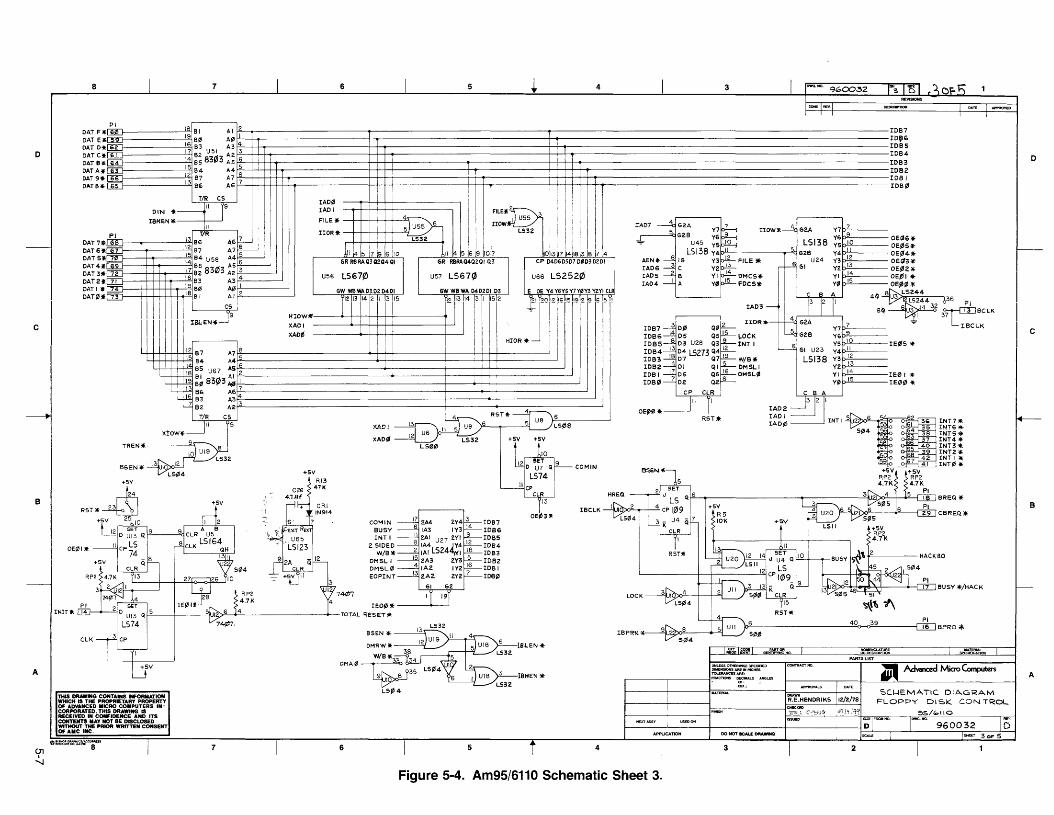
8
OAT F.~OAT E.~OAT D,f
D DATC.~OAT 8.~MTMt~OATS. rWOATS.~
7 6 5 4 3
D
B
c
A
D
BREQ ..
BUSVlJ/HACK
PI16 BPRO""
SC/--IEMATIC DiAGRAMFLOPPY DI'=:>K CONTROL
e>S/IDIIO
39
2
40
R.E.HENDRIKS 12/2/78
3 K U4 Q 7
CLRI
B'SE.No¥.
RSH"
rAD7 ~ G2A Y7~ IIOW,.,----1.: G2A Y71:>-7'---- _
~ G2.B Y6~ ,,{6 9 OElil6f,~ U45 YS~ LSI38 Y5 10 OE!lJS.-
LSI38 Y4 Ii 5 62B "{4 II OE!lJ4*AEN*~16 ,,{.3~FILElIl: r~ U24"{3
12 OE~3.IA06 ----'" C yzP-8- r &1 Y2 13 OEl1!Z *'lADS ~,,{I14 DMCS. II YI 14 OEj/l1 •IA04 I A YII 15 FOCS" C, B~ A"{,lil 15 OE,0i2J!It
8~LS2444lQ IU~I2LC;?4.4. ~36 _.
1A03--1 I l~ I~ I' 8~~ 3~BCLKI j nOiH. I I 4 I G2A I ~'I I -
IOB7~ 012J Qlil~ -rg. Y71:>-7':--___ ~ L1BCLK
IOBS-L.405 Qsr!2-----1-0CK . GZB Y61:>-9,,::-.---I08s J 03 U28 Q3~INT I I 6 ,,{5 10 lEe'S '*IOB4~ 04 LS213 Q4~ '----'= 61 U23 Y4P':'::-11---I083~ 07 Q7~W/B. LSI38 V31:>-""12 _10B2 --3 0 j Q 1~ OM SL I Y2p-'-"13'----rOB I -.Jl 06 Q6~DMSLII VL 14 lEI!! I '"IOBl1l--.J. OZ Qzr-- V0 15 IE00 '"
CP ClR' C B A
,~" TI rA02 ~3 1
2JI
OE,e. I TAOI =.J 5 6RST * 1AD¢ INT I 2
SjZl4
LOCK
~LESSOTHERWlSESPECIFIED
DlIlENSIONSARE IN INCHES
r----,---------lFRACTIOHS DECIMAlS ANGLES
3
LS!il4
IBPRN ~,----"iU2z:=---......"
+5RP
5 U
HREQ~ J SET Qf"6,---<~- ...- 3=-tJ2. 4-r-+=--i
1[:".2 I 4 LS +sv I 3r----.. _ 5.05CPI~9 R5 ~ "M ~~''>o''6'------<i':=--I~LJCBREQ*
10K
4
1BCLK
IBHEN*,
IOB7IOB6lOBSIOB41083IOB2lOBIIOBI2J
5
17 2M 2.Y4 3
6 IA3 IY3 14II ZAI 2.YI 98 IA4 U27 1Y4 122 IAI LS24"rf1 1815 ZA3 2.Y3 54 1AZ IY2 16132.AZ 2Y2 7
61 6Z
I 19
COMINBUSYINT I
2. SIDED
W/B"DMSL 1DMSL¢EOPINT
67
RP2
4.7K IEO¢. _+_---'
f-"-----+------"I\J ::r--4-4'----------+-..-TOTAL RESET lIE
RST 1If 23
OE¢I*
THIS __ CONTAINS IIIFORMATIONWHICH IS THE PROPRIETARY PROPERTYOF ADVANCED IIICRO COIlPUTERS INCORPORATED. THIS ORAWING ISRECEIVED IN CONFIDENCE AND ITSCOIITEIITS IIAY NOT BE DISCLOSEDWITHOUT THE PRIOR WRITTEN CONSENTOFAIIC INC.
INITlI\
()1 'lIl=~"'l::"':·"~"8
~
B
c
A
Figure 5-4. Am95/6110 Schematic Sheet 3.

+5V
B
I 0
~-i
II c
I
LII
I
SIDE SELECTP414
RIG10K
113 114B A
9Y3U54 10Y2
15G 5139 YI II
12
45
+511
•
67 I •
+5VRPB t I
I I r r 1 1 I
I11K
I2YIL~2AI3 6 2 5 4
S""JII
8
B
o
CRYSTAL CLOCKOSCILLATOR8 MH2!
A
+511
/4
'{I
II Is 17 110CLR LOAD ENP ENT I
Z CP LSI63U70
QA QB QC QD
14 13 112 II
L--~-t-t-t-+---- 8&+--t-~!-+---- 4111
+-+-!-t-----2.G
I
+-+----11)
\3~1 I~ eoi
l33t-t----o
Sl!I
61./ '\ 61~13S
,..,,,,n.. 7<¢?
DACKI.~ ,
DACKlZ!.----------'
lJNl.£SSOTHEAWlSESPECIFlEDDtiENSIONSARE IN INCHESTOl£RANCESNE:
r- ,---__---IFRACTlONS DEctMALS AHGLES
~ AdYanced Micro Ccxnputers~------r---t--
A
REV
D
'OO-lE.MATIC OIAGRA.M~LOPP'( DI"5K. CONTROL
2
~~HENDRIKS 11/3C/7B
3
1------+-----I'1NlSH .'.> CH~~~ ChE,"",," 21/41i~,""'ASSY ,USEOOO , ,- , o,;lF
I---'-----,.-~---~--r:=____:_-__:___;
4
1'=:'m.f=::i'A::F"=~JOF ADVANCED MICRO COMPUTERS IN-CORPORATED. THIS DRAWING ISRECEIVED IN CONFIDENCE AND ITSCONTENTS MAY NOT lIE DISCLOSEDWITHOUT Till; .RI(lA WRITTEN CONSENT
IOFAMC INC.
56
1:11 132.
7
Figure 5-5. Am95/6110 Schematic Sheet 4.

8 7 6 5 4 3 ........960032
P3
GNO I GNO
0 IAOIl! 2 FA" IJPI IAOl 3 FAl
3 +svIAD2 4 FA2
4 ~~ 1+IAD3 5 FA3
.llf 7f- I' IAD4 6 FA45 =SEE NOTE I
6 ~ IA05 7 FA5
81IAD6 8 FA6
82IA07 9 FA7
83IAD8 10 FA8
84IA09 FA9
IADA 12 FAIO
IAOB 13 FAil
~~
!ADe
~;:::IAOD
IAOE 16 FAI412
IAOF 17 FAIS7"
~ IOB¢===--Gj GNO
19 FOil!85 I
lOB 1 20 FOl86
C IOB2 21 F02 C
+!ZVIOB3 22 F03
...LC21 1064 23 F04:I- .1 lOBS 24 FOS
9 -5VIOB6 25 FOG
10~C22 IOB7 26 F07~.I 27 GNO
7928
8029
30
IMEMR.-----l 31 READ
IMEMW* 32 WRITE
33 GNO
IIOR * 34 IN
35 GND
now. 36 OUT
37 GND
38
39 GND
B TXINT'i'" TXINT"- B41 GND
-=1=-42
43
INH * 44 INH*
RXINTll< 45 RXINTlIO
OACK3'" 46 PACK3""
OACK2'" 47 DACK2'"
48
RST l!< -----k 49
AEN* 50
THIS _ CONTAINS ..ORMATIONWHICH IS TIE PROPRETARY PROPERTYOF ADVANCED MiellO CO_TERS IN-CORPORATED. THIS DRAWING ISRECEIVED IN CONFIOENCE AND ITS NOIENCUTURE
SPEClACAl10NCONTENTS MAY NOT BE DISCLOSEDWITHOUT THE PRIOR WRITTEN CONSENT PARTS LIST
OFAIIC INO. laIL.£SSOllEAWISESPEaFI£D
~Advanced MicroC~
ADlMENSIONSAfE .. 1NCHESTOl.ERANCESAFlE- A""""""" DECOOAl.S:: .XIC:
'::>CI-1EMAT1C DlA-GRAM
'FLOPPY DI'::>K. CONTROL~':>/<OIIO
DWG.1lO. DDO NOT SCALE DRAWING
(]"I 1J>l'i'&"::l"~8 7 6 5 4 3cb
Figure 5-6. Am95/6110 Schematic Sheet 5.

Address comments to:
Advanced Micro ComputersPublications Department3340 Scott BoulevardSanta Clara, CA 95051
TITLE: Am95/6110 FLOPPY DISK CONTROLLERPUBLICATION NO: 00680108C
COMMENTS: (Describe errors, su~meste'd
additions or deletions, andinclude page numbers, etc.)
COMMENT SHEET
From: Name:
Company:
Address:
Position:

AdvclllcedMicro
Computers
A subsidiary ofAdvanced Micro.Devices
3340 Scott BoulevardSanta Clara,
California 95051(408) 988-7777
TELEX: 171 142


