AlN Thin Film Electroacoustic Devices - DiVA - Simple search

THE TWENTY-FIFTH INTERNATIONAL WORKSHOP ON
ACTIVE-MATRIXFLATPANEL DISPLAYS AND DEVICES-TFT TECHNOLOGIES AND FPD MATERIALS-
JULY 3-6, 2018Ryukoku University Avanti Kyoto HallKyoto, Japan
AM-FPD 18PROGRAM
Sponsorship: International Society of Functional Thin Film Materials & DevicesCo-Sponsorship: The Japan Society of Applied Physics
Technical Sponsorship:The Electrochemical Society - Electronics and Photonics Division -The Electrochemical Society - Japan Section -IEEE Electron Devices SocietyIn cooperation with: The Institute of Electronics, Information and Communication EngineersThe Institute of Image Information and Television EngineersThe Institute of Electrical Engineers of JapanThe Chemical Society of JapanJapanese Liquid Crystal SocietyThin Film Materials & Devices MeetingSociety of Automotive Engineers of Japan, Inc.
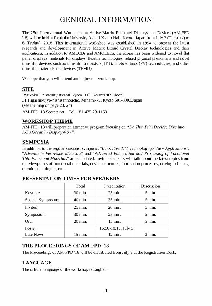
GENERAL INFORMATIONThe 25th International Workshop on Active-Matrix Flatpanel Displays and Devices (AM-FPD'18) will be held at Ryukoku University Avanti Kyoto Hall, Kyoto, Japan from July 3 (Tuesday) to6 (Friday), 2018. This international workshop was established in 1994 to present the latestresearch and development in Active Matrix Liquid Crystal Display technologies and theirapplications. In addition to AMLCDs and AMOLEDs, the scope has been widened to novel flatpanel displays, materials for displays, flexible technologies, related physical phenomena and novelthin-film devices such as thin-film transistors(TFT), photovoltaics (PV) technologies, and otherthin-film materials and devices (TFMD).
We hope that you will attend and enjoy our workshop.
- 1 -
SITERyukoku University Avanti Kyoto Hall (Avanti 9th Floor)31 Higashikujyo-nishisannoucho, Minami-ku, Kyoto 601-8003,Japan (see the map on page 23, 24)AM-FPD '18 Secretariat Tel: +81-475-23-1150
In addition to the regular sessions, symposia, “Innovative TFT Technology for New Applications”,“Advance in Perovskite Materials” and “Advanced Fabrication and Processing of FunctionalThin Films and Materials” are scheduled. Invited speakers will talk about the latest topics fromthe viewpoints of functional materials, device structures, fabrication processes, driving schemes,circuit technologies, etc.
1
SYMPOSIA
Total Presentation DiscussionKeynote 30 min. 25 min. 5 min.
Special Symposium 40 min. 35 min. 5 min.
Invited 25 min. 20 min. 5 min.
Symposium 30 min. 25 min. 5 min.Oral 20 min. 15 min. 5 min.Poster 15:50-18:15, July 5Late News 15 min. 12 min. 3 min.
PRESENTATION TIMES FOR SPEAKERS
THE PROCEEDINGS OF AM-FPD '18The Proceedings of AM-FPD '18 will be distributed from July 3 at the Registration Desk.
LANGUAGEThe official language of the workshop is English.
AM-FPD '18 will prepare an attractive program focusing on “Do Thin Film Devices Dive into IoT's Ocean? - Display 4.0 -”.
WORKSHOP THEME

REGISTRATIONThe Registration Desk will be open in front of Ryukoku University Avanti Kyoto Hall from Tuesday to Friday. The registration hours are as follows:
Tuesday, July 3 9:30-17:00Wednesday, July 4 9:15-17:00Thursday, July 5 9:15-16:30Friday, July 6 9:15-15:00*1
For Advance Registration, access our online registration page (http://www.amfpd.jp) and enrollyour information and complete payment by June 6(JST). Registration and other fees should bepaid in Japanese yen via bank transfer*2 or credit cards. VISA, Master, DC, AMEX, Diners,Nicos and JCB are acceptable. After your payment has been confirmed, confirmation can bedownloaded from our online registration page.
*1 Only cash is acceptable as a means of payment on July 6, 2018.*2 Bank transfer for AM-FPDA/C No.: 3106887 Mizuho Bank, Ltd. Jugogou BranchA/C Name: Nippon Travel Agency Co., Ltd.Registrants living in Japan can make payment via bank transfer or credit cards. Registrantsliving overseas can make payment by credit cards only.
- 2 -
*3The registration fee of the workshop includes the admission to all sessions and USB memory of the proceedings. The banquet of AM-FPD '18 will be served without additional charge.
*4The member of the societies which sponsor and support AM-FPD '18 (see the front cover).*5Students are required to show their ID card.
BANQUETThe banquet will be held on July 4, from 18:30 to 20:30 at Mariage Grande “Glove” on the 8th floor of Avanti.
CategoryAdvance RegistrationBy June 6, 2018(JST) On-Site Registration
WORKSHOP*3
Member*4 ¥50,000 ¥55,000Non-Member ¥52,000 ¥57,000Student*5 ¥20,000 ¥22,000
TUTORIALRegular ¥7,000 ¥7,000Conference Attendee
& Student ¥5,000 ¥5,000
Every foreign visitor entering Japan must have a valid passport. Visitors from countries whose citizens must have visas should apply to a Japanese consular office or diplomatic mission in their own country.
VISAS

- 3 -
In case of cancellation, a written notification should be sent to NTA by e-mail ([email protected]) or by FAX (+81-43-225-2241) to avoid any trouble.
Cancel ChargeFrom June 7 to 25---------JPY 3,000After June 26---100% of the registration fee / NO REFUNDThe Proceedings of the AM-FPD '18(USB memory) will be sent to the attendees who have paidin 100% cancellation charge after the workshop.
CANCELLATION POLICY
Official Travel Agent
Nippon Travel Agency Co., Ltd. (NTA) has been appointed as the official travel agentfor the workshop and will handle all related travel arrangements, including hotelaccommodations. Inquiries and applications concerning arrangements should beaddressed to:
Nippon Travel Agency Co., Ltd.(NTA)Chiba BranchChiba Center Square Bldg. 4F, 2-3-16, Chuo, Chuo-ku, Chiba 260-0013, JapanFax: +81-43-225-2241 Tel: +81-43-227-2307E-mail: [email protected]

These classes are widely aimed at many people from beginners to researchers who hope toreview their knowledge. Presentations and documents will be in Japanese. Documents will bedistributed to the attendees who have registered in advance. The attendees who make an entryon-site will be admitted into these classes, but no documents might be handed. These classes areavailable for an additional fee (see page 2.)
Tuesday, July 3 (10 : 00 ~ 12 : 00)Chairperson : H. Okada, Univ. of Toyama, Japan
10:00 (T-1) Trend of FPD Manufacturing Technology and MarketTetsuya Wadaki, Nomura Securities Co., Ltd., Japan
11:00 (T-2) Highly Efficient Perovskite Solar Cells: Key Points in Their PreparationAtsushi Wakamiya, Kyoto Univ., Japan
The endorsement letters to IEEE Journal Electron Device Society (J-EDS) or ECS Journal SolidState Science and Technology (JSS) will be issued for excellent papers, which are chosen at ourinternal rating processes by AMFPD program committees.
Please select which journal you wish getting the endorsement letter when you submit a paper toAM-FPD.
1. Endorsement letters will be issued to excellent papers from the AM-FPD committee afterAM-FPD’18 workshop is held.
2. After you receive the endorsement letter,- Please attach your paper of AM-FPD'18 and the endorsement letter when submitting your
manuscript to each journal,- You make sure to add in your reference list when you reuse the contents (figures / tables)
used in your paper of AM-FPD'18.
Your ID and password are required to be registered before submitting your manuscript to eachjournal.
Endorsement Letter
- 4 -
IEEE XPLORE DIGITAL LIBRARY
The Proceedings of AM-FPD '18 will be published in the IEEE Xplore digital library in around2 months after the workshop.
TUTORIAL IN JAPANESE

- 5 -
AM-FPD '17 PAPER AWARD
Best Paper Award(4-2) Effects of Electrode Materials on the Electrical and Bending Performance of Memory
Thin Film Transistors Using P(VDF-TrFE) Gate Insulator and IGZO Active ChannelsJi-Hee Yang, Da-Jeong Yun, Gi-Ho Seo, Sung-Min Yoon, Kyung Hee Univ., Korea
Poster Award(P-19) Fluorine Doped Zinc Oxynitride Thin Film Transistors Fabricated by RF Reactive Co-
SputteringHyoung-Do Kim, Jong-Heon Kim, Dae-Gyu Yang, Hyun-Suk Kim, Chungnam Nat'l Univ., Korea
Student Paper AwardHiroyuki Kanda, Univ. of Hyogo., Japan (2-3) Bromine Doped Perovskite / Textured Silicon Heterojunction for Mechanically Stacked
Tandem Solar Cell
AMFPD-ECS Japan Section Young Researcher AwardDaisuke Matsuo, Nissin Electric Co., Ltd., Japan(P-L2) High Reliability a-InGaZnO TFT by Inductively Coupled Plasma Sputtering System
AWARDS
Papers presented at this workshop will be considered for “AM-FPD Paper Awards”, “AMFPD-ECS Japan Section Young Researcher Award”. These winners will be presented at the awardceremony in AM-FPD '19 workshop.
AM-FPD Paper Awards“Best Paper Award”, “Poster Award” and “Student Paper Award” will be presented. Thewinners of them are selected by AMFPD '18 award committee chaired by Professor YukiharuUraoka (NAIST).
AMFPD-ECS Japan Section Young Researcher AwardECS Japan Section and AM-FPD Organizing Committee have jointly established “AMFPD-ECS Japan Section Young Researcher Award”. This award will be given to the author under theage of 35 that belongs to the university or the research institute in Japan.

Chair:Vice-Chair:Members:
Advisor :
ORGANIZING COMMITTEE
- 6 -
Hiroki Hamada (Kinki Univ.)Hiroshi Tsutsu (Japan Display)Toshiaki Fujino (Mitsubishi Electric)Taketsugu Itoh (Corning Japan)Junya Kiyota (ULVAC)Yue Kuo (Texas A&M Univ.)Atsushi Masuda (AIST)Takuya Matsuo (Sharp)Akira Okada (Okayama Univ.) Nobuo Sasaki (Sasaki Consulting) Kenji Sera (Tianma Japan)Makoto Ohkura
Chair:Vice-Chair:Members:
STEERING COMMITTEEYukiharu Uraoka (NAIST)Hiroshi Tanabe (Tianma Japan)Toshiaki Arai (JOLED)Takahiko Ban (Ryukoku Univ.)Susumu Horita (JAIST)Toshio Kamiya (Tokyo Inst. of Technol.)Mutsumi Kimura (Ryukoku Univ.)Jun Koyama (Semicond. Energy Lab.) Shin-Ichiro Kuroki (Hiroshima Univ.)Naoto Matsuo (Univ. of Hyogo)Hiroyuki Okada (Univ. of Toyama)

Chair:Vice-Chairs:
Members:
PROGRAM COMMITTEE
- 7 -
Hiroyuki Okada (Univ. of Toyama)Masatoshi Kitamura (Kobe Univ.)Sung-Min Yoon (Kyung Hee Univ.)Shun-Wei Liu (Ming-Chi Univ. of Technol.)Norbert Fruehauf (Univ. of Stuttgart)Yue Kuo (Texas A&M Univ.)Meng Tao (Arizona State Univ.)Byung Seong Bae (Hoseo Univ.)Yvan Bonnassieux (Ecole Polytechnique)Mamoru Furuta (Kochi Univ. of Technol.)Reiji Hattori (Kyushu Univ.)Akira Heya (Univ. of Hyogo)Yongtaek Hong (Seoul Nat'l Univ.)Susumu Horita (JAIST)Chi-Sun Hwang (ETRI)Ryoichi Ishihara (Delft Univ. of Technol.)Yasuaki Ishikawa (NAIST)Jin Jang (Kyung Hee Univ.)Hirotake Kajii (Osaka Univ.)Toshio Kamiya (Tokyo Inst. of Technol.)Tetsuya Kaneko (Tokai Univ.)Hyun Jae Kim (Yonsei Univ.)Junghwan Kim (Tokyo Inst. of Technol.)Dietmar Knipp (Jacobs Univ. Bremen)Chih-Lung Lin (Nat’l Cheng Kung Univ.)Tokiyoshi Matsuda (FLOSFIA)Nobuyuki Matsuki (Kanagawa Univ.)Masahiro Mitani (Sharp)Kentaro Miura (Japan Display)Tatsuo Mori (Aichi Inst. of Technol.)Hiroyoshi Naito (Osaka Prefecture Univ.)Hiroaki Nakamura (Idemitsu Kosan)Kenji Nakao (Japan Display)Mitsuru Nakata (NHK Sci. & Technol. Res. Labs)Takashi Noguchi (Univ. of the Ryukyus)Taizoh Sadoh (Kyushu Univ.)Nobuyoshi Saito (Toshiba Memory)Ruud E. I. Schropp (Eindhoven Univ. of Technol.)Isao Suzumura (Japan Display)Kazushige Takechi (Tianma Japan)Taishi Takenobu (Nagoya Univ.)Yasuhiro Terai (JOLED)Yung-Hui Yeh (ITRI)Atsushi Wakamiya (Kyoto Univ.)
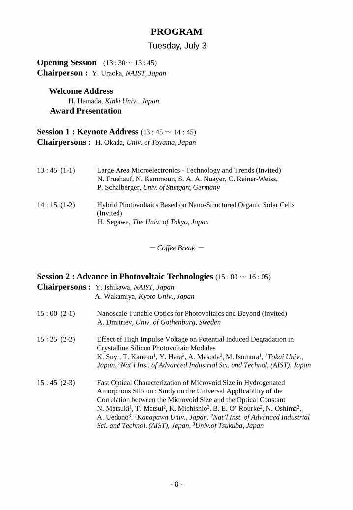
Opening Session (13 : 30~ 13 : 45)Chairperson : Y. Uraoka, NAIST, Japan
Welcome AddressH. Hamada, Kinki Univ., Japan
Award Presentation
PROGRAM
- 8 -
Tuesday, July 3
Session 1 : Keynote Address (13 : 45 ~ 14 : 45)Chairpersons : H. Okada, Univ. of Toyama, Japan
13 : 45 (1-1) Large Area Microelectronics - Technology and Trends (Invited) N. Fruehauf, N. Kammoun, S. A. A. Nuayer, C. Reiner-Weiss,P. Schalberger, Univ. of Stuttgart, Germany
14 : 15 (1-2) Hybrid Photovoltaics Based on Nano-Structured Organic Solar Cells (Invited) H. Segawa, The Univ. of Tokyo, Japan
- Coffee Break -
Session 2 : Advance in Photovoltaic Technologies (15 : 00 ~ 16 : 05)Chairpersons : Y. Ishikawa, NAIST, Japan
A. Wakamiya, Kyoto Univ., Japan
15 : 00 (2-1) Nanoscale Tunable Optics for Photovoltaics and Beyond (Invited)A. Dmitriev, Univ. of Gothenburg, Sweden
15 : 25 (2-2) Effect of High Impulse Voltage on Potential Induced Degradation in Crystalline Silicon Photovoltaic Modules K. Suy1, T. Kaneko1, Y. Hara2, A. Masuda2, M. Isomura1, 1Tokai Univ., Japan, 2Nat’l Inst. of Advanced Industrial Sci. and Technol. (AIST), Japan
15 : 45 (2-3) Fast Optical Characterization of Microvoid Size in Hydrogenated Amorphous Silicon : Study on the Universal Applicability of the Correlation between the Microvoid Size and the Optical Constant N. Matsuki1, T. Matsui2, K. Michishio2, B. E. O’ Rourke2, N. Oshima2, A. Uedono3, 1Kanagawa Univ., Japan, 2Nat’l Inst. of Advanced Industrial Sci. and Technol. (AIST), Japan, 3Univ.of Tsukuba, Japan

- 9 -
Special Session 1 : Quantam Dot Devices and Applications (16 : 05 ~ 17 : 20)Chairpersons : R. Hattori, Kyushu Univ., Japan
T. Arai, JOLED, Japan
16 : 05 (SP1-1) Progress in the Development of Heavy Metal-Free Quantum Dots for Electroluminescent Displays (Invited)N. L. Pickett, S. K. Stubbs, N. C. Gresty, Nanoco Technologies Ltd., UK
16 : 30 (SP1-2) High Efficiency Inverted Quantum-Dot LED (Invited)H. -M. Kim, J. Jang, Kyung Hee Univ., Korea
16 : 55 (SP1-3) Optical Characteristics of TN-LCD Combined with Inkjet Printed Quantum Dot Color Pixel Convertor (Invited)M. Hasegawa, Merck Performance Materials Ltd., Japan
Author Interviews (17 : 20 ~ 17 : 50)

- 10 -
The 25th Anniversary Special Symposium : The Vehicle Displays (9 : 15 ~ 18 : 15)
Introduction (9 : 15 ~ 9 : 25)Chairpersons : B. Straub, Daimler AG, Germany
Special Symposium 1 : Automotive Trends: Chances for New Display Applications (9:25 ~ 10:45)
Chairpersons : N. Fruehauf, Univ. of Stuttgart, GermanyA. Okada, Okayama Univ., Japan
9 : 25 (SS1-1) Automotive Displays - Trends, Opportunities and Challenges (Invited)D. S. Hermann, Volvo Car Corp. AB, Sweden
10 : 05 (SS1-2) Automotive Displays - Increasing and Challenging Market (Invited)B. Straub, Daimler AG, Germany
- Coffee Break -
Wednesday, July 4
Special Symposium 2 : Seamless Display Integration: Challenges for Novel Display Applications (11 : 00 ~ 14 : 50)
Chairpersons : B. Straub, Daimler AG, GermanyH. Tsutsu, Japan Display, Japan
11 : 00 (SS2-1) High Gamut Display for Next Generation Automotives (Invited)R. Rao, Harman, USA
11 : 40 (SS2-2) Evolution of In-Vehicle Display Technology and Innovation of the Cockpit System (Invited)Y. Muto, Panasonic Corp., Japan
- Lunch-
13 : 30 (SS2-3) Advantage of Head-Up Display for Automobiles (Invited)T. Tsuchida, T. Yachida, Y. Masuya, Nippon Seiki Co., Ltd., Japan
14 : 10 (SS2-4) Implementation of a Sparkle Characterization Method for Anti-Glare Layers on Automotive-Displays (Invited)V. F. Paz, S. Kohlenbecker, E. Persidis, Robert Bosch GmbH, Germany
- Coffee Break -

- 11 -
Special Symposium 3 : Enabling Innovative Display Technologies, Consumer Electronics as Pacemaker (15 : 05 ~ 17: 05)
Chairpersons : D. S. Hermann, Volvo Car Corp. AB, Sweden H. Tanabe, Tianma Japan Ltd., Japan
15 : 05 (SS3-1) Chances and Challenges for Automotive Displays (Invited)M. Adachi, Japan Display Inc., Japan
15 : 45 (SS3-2) Display Technologies for Vehicle Interior Innovation (Invited)M. Ihara, Sharp Corp, Japan
16 : 25 (SS3-3) The Vehicular Display (Invited)M. Araki, H. Taniguchi, K. Tanaka, Mitsubishi Electric Corp., Japan
Panel Discussion (17 : 05 ~ 18 : 05)Coordinator : N. Fruehauf, Univ. of Stuttgart, GermanyPanelists : All invited speakers in Special Symposium on “The Vehicle Display”
Closing (18: 05 ~ 18 : 15)Chairpersons : N. Fruehauf, Univ. of Stuttgart, Germany
Banquet (18: 30 ~ 20 : 30)

Symposium 2 : Innovative TFT Technology for New Applications(11 : 00 ~ 12 : 30)
Chairpersons : M. Nakata, NHK Sci. & Technol. Res. Labs., JapanM. Kimura, Ryukoku Univ., Japan
11 : 00 (S2-1) Electric Field Thermopower Modulation of Two-Dimensional Electron Gas (Invited)H. Ohta, Hokkaido Univ., Japan
11 : 30 (S2-2) Solution Processed Steep Subthreshold OFETs for Low-Power and High Sensitivity Bio-Chemical Sensing (Invited)J. Zhao, Q. Li, W. Tang, X. Guo, Shanghai Jiao Tong Univ., China
12 : 00 (S2-3) Flexible Organic Non-Volatile Memory with Long Retention (Invited)S. Yoo, S. Lee, J. Yun, H. Moon, Korea Advanced Inst. of Sci. and Technol. (KAIST), Korea
- Lunch -
- 12 -
Symposium 1 : Advance in Perovskite Materials (9 : 15 ~ 10 : 45)Chairpersons : A. Wakamiya, Kyoto Univ., Japan
Y. Ishikawa, NAIST, Japan
9 : 15 (S1-1) Nonlinear Optical Properties of Lead Halide Perovskites (Invited)H. Tahara, T. Yamada, T. Handa, Y. Kanemitsu, Kyoto Univ., Japan
9 : 45 (S1-2) Stability Issue of Perovskite Solar Cells (Invited)S. Ito, Univ. of Hyogo, Japan
10 :15 (S1-3) Efficient and Stable Perovskite-Based Optoelectronic Devices (Invited)T. Matsushima1,2, C. Qin1,2, T. Fujihara3, C. Adachi1,2, 1Kyushu Univ., Japan, 2Japan Sci. and Technol. Agency (JST), Japan, 3Inst. of Systems, Information Technologies and Nanotechnologies (ISIT), Japan
- Coffee Break -
Thursday, July 5

- 13 -
Symposium 3 : Advanced Fabrication and Processing of Functional Thin Films and Materials (13 : 50 ~ 15 : 20)
Chairpersons : H. Kajii, Osaka Univ, JapanT. Matsushima, Kyushu Univ., Japan
13 : 50 (S3-1) Controlling Organic/Inorganic Junctions by Covalent Tethering at the Interface (Invited)H. Usui, Tokyo Univ. of Agriculture and Technol., Japan
14 : 20 (S3-2) Thermoelectric Transport in Doped Carbon Nanotube Films (Invited)Y. Nonoguchi1,2, 1Nara Inst. of Sci. and Technol. (NAIST), Japan, 2Japan Sci. and Technol. Agency (JST), Japan
14 : 50 (S3-3) Concealed Holograms Based on Cholesteric Liquid Crystals (Invited)H. Yoshida1,2, S. Y. Cho1, M. Ono1, M. Ozaki1, 1Osaka Univ., Japan, 2Japan Sci. and Technol. Agency (JST), Japan
Author Interviews (15 : 20 ~ 15 : 50)

- 14 -
Poster Session (15 : 50 ~ 18 : 15)Chairpersons : H. Okada, Univ. of Toyama, Japan
M. Kitamura, Kobe Univ., JapanH. Kajii, Osaka Univ., JapanA. Wakamiya, Kyoto Univ., Japan
FPDp(P-1) Inverted Quantum-Dot Light-Emitting Diodes with WO3/Zinc-Tin-Oxide
Electron Transporting LayersD. -J. Kim, H. -N. Lee, Soonchunhyang Univ., Korea
(P-2) Solution Processed Low-Color Temperature OLED with High EfficiencyM. Lee, D. K. Dubey, Y. C. Lo, J. -H. Jou, Nat’l Tsing Hua Univ., Taiwan
(P-3) Development of Roll-to-Roll Multi-Layer Thermal Evaporation System for Flexible OLED DevicesS. Kwon1, D. Song1, H. Kim1, M. Lee2, K. Woo1, 1Korea Inst. of Machinery & Materials, Korea, 2GJM Co., Ltd., Korea
(P-4) Laser-Scanned Programmable Perovskite-Nanocrystal Color Conversion Layers for White Light-Emitting Electrochemical CellsW. -K. Wu1, C. -M. Wang1, M. -C. Chan1, J. -Y. Lien2, Y. -M. Su1, M. Sarma3, Z. -P. Yang1, H. -C. Su1, K. -T. Wong3, S. -L. Wang2, 1Nat’l Chiao Tung Univ., Taiwan, 2Nat’l Tsing Hua Univ., Taiwan, 3Nat’l Taiwan Univ., Taiwan
(P-5) Adjusting Correlated Color Temperature from White Light-Emitting Electrochemical Cells by Employing Electrochromic FiltersB. -R. Chiou1, Z. -P. Yang1, M. Sarma2, H. -C. Su1, K. -T. Wong2, 1Nat’l Chiao Tung Univ., Taiwan, 2Nat’l Taiwan Univ., Taiwan
(P-6) Synchronization Scheme of Plural Displays for Real-Time InteractionY. Kim, J. Hong, S. Hong, C. Shin, S. -K. Joo, J. Byun, H. Kang, Korea Electronics Technol. Inst., Korea
(P-7) Hydrogenated Amorphous Silicon Gate Driver with Charge-Holding Scheme for In-Cell Touch PanelsY. -S. Lin, P. -C. Lai, F. -H. Chen, Z. -L. Yang, C. -L. Lin, Nat’l Cheng Kung Univ., Taiwan
(P-8) Novel a-Si:H Gate Driver Circuit with High Charging and Discharging Speeds for Use in High-Resolution Liquid-Crystal DisplaysW. -C. Chiu, C. -C. Hsu, P. -C. Lai, M. -X. Wang, C. -L. Lin, Nat’l Cheng Kung Univ., Taiwan
(P-9) Design of Gate Driver Circuit Using a-Si:H Thin-Film Transistors with Bootstrapping Structure for High-Resolution DisplaysB. -S. Chen, M. -Y. Deng, W. -S. Liao, C. -L. Lin, Nat’l Cheng Kung Univ., Taiwan

- 15 -
(P-L1) 2-D Strain Sensors with Asymmetrically Pre-Stretched Metal Thin Filmfor Multidimensionally Stretchable ElectronicsS. Choi, S. Kim, T. Kim, B. Lee, Y. Hong, Seoul Nat’l Univ., Korea
TFTp(P-10) Effects of Wavelength and Geometrical Condition on Photosensitivity of
Self-Aligned Top-Gate Amorphous InZnO Thin Film TransistorsY. Yang, H. Lu, X. Deng, S. Zhang, Peking Univ., China
(P-11) Thin Film Logic Circuit with Metal Capping Layered Amorphous SiZnSnO Thin-Film TransistorsB. H. Lee1,3, J. M. Byun2,3, S. Kim1, S. Y. Lee2,3, 1Korea Univ., Korea, 2Cheongju Univ., Korea, 3Res. Inst. of Advanced Semiconductor Convergence Technol. (RIASCT), Korea
(P-12) Investigation on Solution-Processed In-Si-O Thin-Film Transistor via Spin-Coating MethodH. Hoang1, T. Hori1, T. Yasuda1, T. Kizu2, K. Tsukagoshi2, T. Nabatame2, B. N. Q. Trinh3, A. Fujiwara1, 1Kwansei Gakuin Univ., Japan, 2Nat’l Inst. for Materials Sci. (NISM), Japan, 3Vietnam Nat’l Univ.-Hanoi, Vietnam
(P-13) Withdrawn
(P-14) Characterizations on the Device Stabilities of the Oxide Thin Film Transistors Using In-Ga-Zn-O Channels Prepared by Atomic-Layer DepositionS. -J. Yoon1, N. -J. Seong2, K. Choi2, W. -C. Shin2, S. -M. Yoon1, 1Kyung Hee Univ., Korea, 2NCD Co. Ltd., Korea
(P-15) High Field-Effect Mobility Amorphous Indium-Tin-Zinc-Oxide Thin-Film Transistors Using Negatively Charged Aluminium-Oxynitride Gate DielectricsD. Shin, K. Jang, C. P. T. Nguyen, H. Park, J. Kim, Y. Kim, J. Yi, Sungkyunkwan Univ., Korea
(P-16) Flexible Thin-Film Transistors with Vertical In-Ga-Zn-O Channel Using Atomic-Layer Deposition on Poly(Ethylene Naphthalate) SubstrateH. -R. Kim1, J. -H. Yang1, G. -H. Kim2, S. -M. Yoon1, 1Kyung Hee Univ., Korea, 2Electronics & Telecommunication Res. Inst. (ETRI), Korea
(P-17) Transparent Triple-Layer Oxide TFT for Enhanced Photo Switching CharacteristicsJ. Lee1,2, J. Moon2, J. -E. Pi2, S. H. Cho2, H. -O. Kim2, H. Oh2, C. -S. Hwang2, S. -D. Ahn2, S. -Y. Kang2, K. -H. Kwon1, 1Korea Univ., Korea, 2Electronics Telecommunications Res. Inst. (ETRI), Korea

(P-18) Withdrawn
(P-19) Impact of Al2O3 Buffer Layer on Ultra-Thin Flexible Polyimide Substrates for Transparent and Flexible InGaZnO Thin Film TransistorsH. -W. Jang1, H. -R. Kim1, J. -H. Yang1, C. -W. Byun2, S. -M. Yoon1, 1Kyung Hee Univ., Korea, 2Electronics & Telecommunication Res. Inst.(ETRI), Korea
(P-20) Characteristic Evaluation of Ga-Sn-O Thin Films by Hall MeasurementK. Imanishi, A. Fukawa, T. Matsuda, M. Kimura, Ryukoku Univ., Japan
(P-21) Surface Passivation of Crystalline Silicon by Heat Treatment in Liquid Water and Its Application to Improve the Interface Properties of Metal-Oxide-Semiconductor StructuresT. Sameshima1, M. Hasumi1, Y. Hirokawa1, T. Watanabe1, M. Hino1, G. Kojitani1, T. Mizuno2, 1Tokyo Univ. of Agriculture and Technol., Japan, 2Kanagawa Univ., Japan
(P-22) Properties of Poly-Si Thin Films and Their Transistors Fabricated Using Selective Excimer Laser AnnealingT. Goto1, K. Saito2, F. Imaizumi1, M. Hatanaka2, M. Takimoto2, M. Mizumura2, J. Gotoh2, H. Ikenoue3, K. Udagawa4, J. Kido4, S. Sugawa1, 1Tohoku Univ., Japan, 2V-Technol. Co., Ltd., Japan, 3Kyushu Univ., Japan, 4Yamagata Univ., Japan
(P-23) An a-IGZO TFT AMOLED Pixel Circuit to Compensate Threshold Voltage and Mobility VariationsS. Yi, J. Wu, C. Liao, Y. Wang, X. Huo, S. Zhang, Peking Univ., China
(P-24) New AMOLED Pixel Circuit to Compensate Characteristics Variations of LTPS TFTs and Voltage DropJ. Wu, S. Yi, C. Liao, X. Huo, Y. Wang, S. Zhang, Peking Univ., China
(P-25) Withdrawn
(P-26) Investigation of Mechanical-Stress-Induced Electrical Failure of Oxide-Based Flexible Charge-Trap Memory Thin-Film Transistors Fabricated on Plastic SubstratesJ. -H. Yang1, G. -H. Kim2, S. -M. Yoon1, 1Kyung Hee Univ., Korea, 2Electronics & Telecommunication Res. Inst.(ETRI), Korea
(P-27) Nonvolatile Memory TFT Using Neutral Particle Beam at Room Temperature to Generate Mobile Protons Moving in the Gate InsulatorJ. W. Yun1, J. N. Jang2, M. P. Hong1, 1Korea Univ., Korea, 2WISOL Co., Ltd., Korea
- 16 -

(P-28) Carrier Mobility Effect of Electron Transporting Layer on OLED PerformanceR. A. K. Yadav1, D. K. Dubey1, M. Dembla2, S. Z. Chen1, T. -W. Liang3, J. -H. Jou1, 1Nat’l Tsing Hua Univ., Taiwan, 2Indian Inst. of Technol., India, 3 Global Sci. Instruments Co. Ltd., Taiwan
(P-29) High-Efficiency Organic Light-Emitting Diodes with a Complete Cascading Carrier Injection StructureW. -Y. Yang1, R. A. K. Yadav1, D. K. Dubey1, C. -H. Hsu1, Y. -Y. Lee1, T. -W. Liang2, J. -H. Jou1, 1Nat’l Tsing Hua Univ., Taiwan, 2Global Sci. Instruments Co. Ltd., Taiwan
(P-L2) Effect of Deposition Temperature and Source Gas Chemistry in PE-CVD SiO2 Passivation on InGaZnO TFTsS. G. M. Aman, D. Koretomo, Y. Magari, M. Furuta, Kochi Univ. of Technol., Japan
(P-L3) Biological Stimulation Performance of LTPS-TFTs Artificial Retina by Wireless Power DriveK. Tomioka, K. Miyake, K. Misawa, M. Kimura, Ryukoku Univ., Japan
(P-L4) Characterization of Excimer-Laser Doping of a Poly-Si Thin Film with a Phosphoric-Acid Coating for Thin-Film-Transistor FabricationK. Imokawa1, N. Tanaka1, A. Suwa1, D. Nakamura1, T. Sadoh1, T. Goto2, H. Ikenoue1, 1Kyushu Univ., Japan, 2Tohoku Univ., Japan
(P-L5) Enhancement of TFT Performance by Purification of Indium-Zinc-Tin OxideB. R. Naik, M. N. Naik, C. Avis, J. Jang, Kyung Hee Univ., Korea
(P-L6) Threshold Voltage Control of In-Ga-Zn-O TFT without Thermal Annealing Process by Inductively Coupled Plasma Sputtering SystemD. Matsuo1, T. Ikeda1, S. Kishida1, Y. Setoguchi1, Y. Andoh1, R. Miyanaga2, M. N. Fujii2, Y. Uraoka2, 1Nissin Electric Co., Ltd., Japan, 2Nara Inst. of Sci. and Technol. (NAIST), Japan
(P-L7) Reliability Enhancement of Solution Processed Amorphous In-Zn-O Thin-Film Transistors via a Low Temperature (180 ºC) Solution Processed PassivationA. Syairah1, J. P. Bermundo1, N. Yoshida1,2, T. Nonaka2, M. N. Fujii1,Y. Ishikawa1, Y. Uraoka1, 1Nara Inst. of Sci. and Technol. (NAIST), Japan, 2Merck Performance Materials Ltd., Japan
- 17 -

PVp(P-30) Flexible ITO-Free Perovskite Solar Cells
M. -Y. Lin, Nat’l United Univ., Taiwan
(P-31) Fabrication of Perovskite Solar Cells with E-Beam Evaporation TiO2 Thin Films: Considering Substrate HeaterM. F. Hossain1,2, S. Naka1, H. Okada1, 1Univ. of Toyama, Japan, 2Rajshahi Univ. of Engineering and Technol., Bangladesh
(P-32) Effect of Molecular Energy Level of Electron Transport Layer on Recombination Zone in OLEDD. K. Dubey1, R. A. K. Yadav1, M. Lee1, S. Khan2, T. -W. Liang3, J. -H. Joua1, 1Nat’l Tsing Hua Univ., Taiwan, 2Indian Inst. of Technol. Delhi, India, 3Global Sci. Instruments Co. Ltd., Taiwan
(P-L8) Novel Facilely Synthesized Spiro[Fluorene-9,9′-Phenanthren-10′-One] in D-A-D Hole-Transporting Materials for Perovskite Solar CellsY. -C. Chen1, S. -K. Huang2, S. -S. Li2, Y. -Y. Tsai3, C. -P. Chen3, Y. J. Chang1, 1Tunghai Univ., Taiwan, 2Taipei Medical Univ., Taiwan, 3Ming Chi Univ. of Technol., Taiwan
TFMDp(P-33) Fabrication of Inorganic/Organic Hybrid Distributed Bragg Reflectors
Based on Inorganic CuSCN for All-Solution-Processed Polymer Light-Emitting DiodesH. Kajii, M. Kawata, H. Okui, M. Morifuji, M. Kondow, Osaka Univ., Japan
(P-34) Cellular Neural Network Using IGZO Thin Film as Synapses and LSI as NeuronsD. Yamakawa1, Y. Shibayama1, H. Yamane2, Y. Nakashima2, M. Kimura1,2, 1Ryukoku Univ., Japan, 2Nara Inst. of Sci. and Technol. (NAIST), Japan
(P-35) Room Temperature Fabrication of Variable Resistive Memory Using Ga-Sn-O Thin FilmS. Sugiski1, A. Kurasaki1, R. Tanaka1, T. Matsuda1, M. Kimura1,2, 1Ryukoku Univ., Japan, 2Nara Inst. of Sci. and Technol. (NAIST), Japan
(P-36) Cross-Point Device Using Ta2O5/Ta Layer for Synapse Element in Neural NetworkR. Tanaka1, I. Horiuchi2, Y. Mogi2, Y. Hiroshima2, Y. Nakashima3, M. Kimura1,3, 1Ryukoku Univ., Japan, 2KOA Corp., Japan, 3Nara Inst. of Sci. and Technol. (NAIST), Japan
(P-37) High Performance Sol-Gel Processed SnO2 Thin Film Transistor with Sol-Gel Processed ZrO2 LayersW. -Y. Lee, B. Jang, S. Lee, T. Kim, J. Jang, Kyungpook Nat’l Univ., Korea
- 18 -
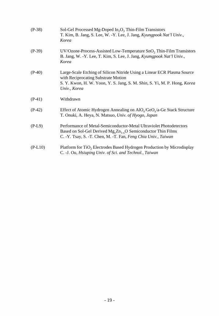
(P-38) Sol-Gel Processed Mg-Doped In2O3 Thin-Film TransistorsT. Kim, B. Jang, S. Lee, W. -Y. Lee, J. Jang, Kyungpook Nat’l Univ., Korea
(P-39) UV/Ozone-Process-Assisted Low-Temperature SnO2 Thin-Film TransistorsB. Jang, W. -Y. Lee, T. Kim, S. Lee, J. Jang, Kyumgpook Nat’l Univ., Korea
(P-40) Large-Scale Etching of Silicon Nitride Using a Linear ECR Plasma Source with Reciprocating Substrate MotionS. Y. Kwon, H. W. Yoon, Y. S. Jang, S. M. Shin, S. Yi, M. P. Hong, Korea Univ., Korea
(P-41) Withdrawn
(P-42) Effect of Atomic Hydrogen Annealing on AlOx/GeOx/a-Ge Stack Structure T. Onuki, A. Heya, N. Matsuo, Univ. of Hyogo, Japan
(P-L9) Performance of Metal-Semiconductor-Metal Ultraviolet Photodetectors Based on Sol-Gel Derived MgxZn1-xO Semiconductor Thin FilmsC. -Y. Tsay, S. -T. Chen, M. -T. Fan, Feng Chia Univ., Taiwan
(P-L10) Platform for TiO2 Electrodes Based Hydrogen Production by MicrodisplayC. -J. Ou, Hsiuping Univ. of Sci. and Technol., Taiwan
- 19 -
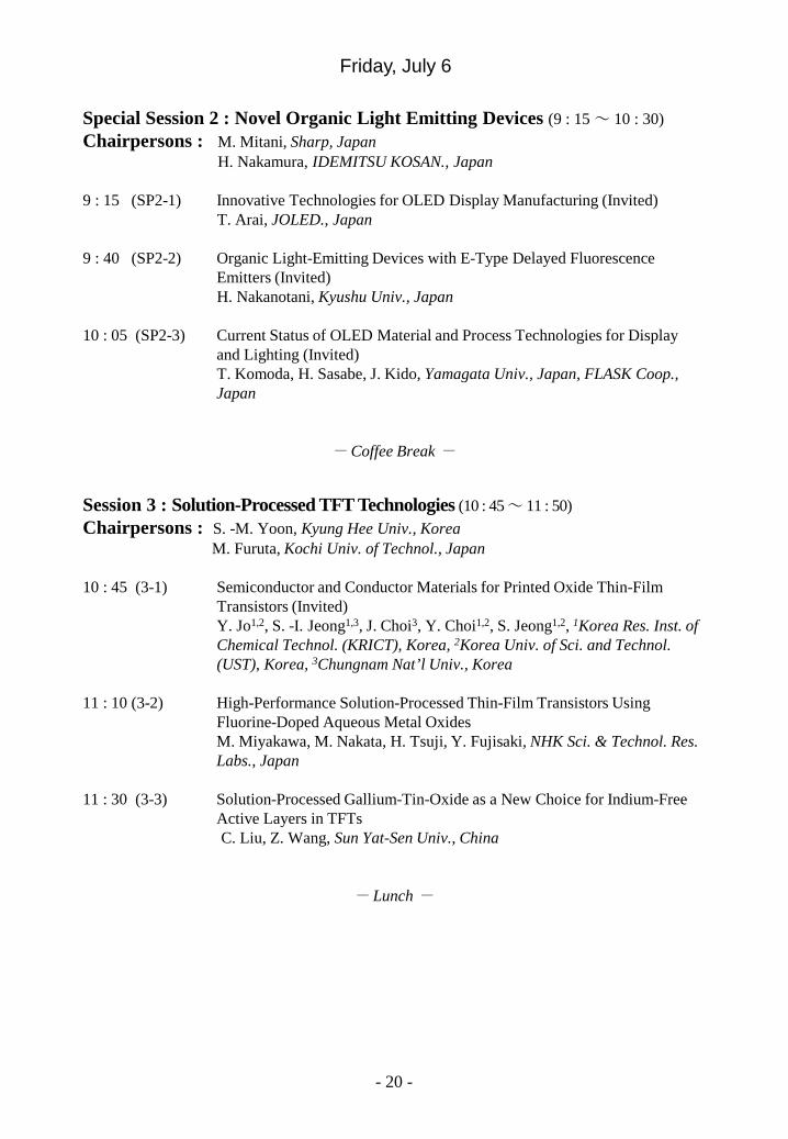
Friday, July 6
Special Session 2 : Novel Organic Light Emitting Devices (9 : 15 ~ 10 : 30)Chairpersons : M. Mitani, Sharp, Japan
H. Nakamura, IDEMITSU KOSAN., Japan
9 : 15 (SP2-1) Innovative Technologies for OLED Display Manufacturing (Invited)T. Arai, JOLED., Japan
9 : 40 (SP2-2) Organic Light-Emitting Devices with E-Type Delayed Fluorescence Emitters (Invited)H. Nakanotani, Kyushu Univ., Japan
10 : 05 (SP2-3) Current Status of OLED Material and Process Technologies for Display and Lighting (Invited)T. Komoda, H. Sasabe, J. Kido, Yamagata Univ., Japan, FLASK Coop., Japan
- Coffee Break -
Session 3 : Solution-Processed TFT Technologies (10 : 45 ~ 11 : 50)Chairpersons : S. -M. Yoon, Kyung Hee Univ., Korea
M. Furuta, Kochi Univ. of Technol., Japan
10 : 45 (3-1) Semiconductor and Conductor Materials for Printed Oxide Thin-Film Transistors (Invited)Y. Jo1,2, S. -I. Jeong1,3, J. Choi3, Y. Choi1,2, S. Jeong1,2, 1Korea Res. Inst. of Chemical Technol. (KRICT), Korea, 2Korea Univ. of Sci. and Technol. (UST), Korea, 3Chungnam Nat’l Univ., Korea
11 : 10 (3-2) High-Performance Solution-Processed Thin-Film Transistors Using Fluorine-Doped Aqueous Metal OxidesM. Miyakawa, M. Nakata, H. Tsuji, Y. Fujisaki, NHK Sci. & Technol. Res. Labs., Japan
11 : 30 (3-3) Solution-Processed Gallium-Tin-Oxide as a New Choice for Indium-Free Active Layers in TFTsC. Liu, Z. Wang, Sun Yat-Sen Univ., China
- Lunch -
- 20 -

Session 4 : Novel Fabrication Processing and Applications (13: 20 ~ 14 : 40)Chairpersons : H. Okada, Univ. of Toyama, Japan
H. Kajii, Osaka Univ., Japan
13 : 20 (4-1) Two-Step Ion Implantation Used for Activating Boron Atoms in Silicon at 300ºC T. Nagao1, T. Uehara2, K. Yasuta2, Y. Inouchi1, J. Tatemichi1, M. Hasumi2, T. Sameshima2, 1NISSIN ION EQUIPMENT CO., LTD., Japan, 2Tokyo Univ. of Agriculture and Technol., Japan
13 : 40 (4-2) Carbon Heating Tube Used for Rapid Heating System for Semiconductor AnnealingT. Miyazaki1,3, G. Kobayashi2, T. Sugawara3, T. Kikuchi3, M. Hasumi3, T. Sameshima3, 1Techno Res., Ltd., Japan, 2Orc manufacturing Co., Ltd., Japan, 3Tokyo Univ. of Agriculture and Technol., Japan
14 : 00 (4-3) Research and Development of Ga-Sn-O Thin Films for Application to Neural NetworksK. Ikushima1, J. Shimura1, T. Matsuda1, M. Kimura1,2, H. Yamane2, Y. Nakashima2, 1Ryukoku Univ., Japan, 2Nara Inst. of Sci. and Technol. (NAIST), Japan
14 : 20 (4-4) Selective Intense Light-Induced High-Performance Washable Transparent ElectrodesK. Woo, Z. Zhong, H. Kim, S. Kwon, D. Kang, S. -H. Lee, T. -M. Lee, J. Jo, Korea Inst. of Machinery & Materials (KIMM), Korea
- Coffee Break -
Session 5 : Advanced Applications of TFTs (14 : 55 ~ 16 : 00)Chairpersons : M. Kitamura, Kobe Univ., Japan
N. Saito, Toshiba Memory, Japan
14 : 55 (5-1) Flexible a-IGZO TFT Technology: New Developments & Applications (Invited)A. J. Kronemeijer, I. Katsouras, P. Poodt, H. Akkerman, A. V. Breemen, G. Gelinck, TNO / Holst Ctr., The Netherlands
15 : 20 (5-2) Demonstration of Extended-Gate Structure for pH Sensors Based on Amorphous Indium-Gallium-Zinc Oxide Thin-Film TransistorsS. Iwamatsu1, K. Takechi2, H. Tanabe2, Y. Watanabe1, 1Yamagata Res. Inst. of Technol., Japan, 2Tianma Japan, Ltd., Japan
15 : 40 (5-3) Characterizations of Charge-Trap Memory Thin-Film Transistors Using HfO2/ZnO Stack-Structured Charge-Trap Layer Controlled by Atomic Layer Deposition S. -Y. Na, S. -M. Yoon, Kyung Hee Univ., Korea
- 21 -

Late News (16 : 00 ~ 16 : 30)16 : 00 (L-1) Solution-Processable P-Type Transparent Amorphous Semiconductor for
Flexible ElectronicsT. Jun, K. Aoyama, J. Bang, J. Kim, H. Hosono, Tokyo Inst. of Technol., Japan
16 : 15 (L-2) Self-Aligned Four-Terminal P-Channel Cu-MIC Poly-Ge1-xSnx Thin-Film Transistors on a Glass SubstituteR. Miyazaki, N. Nishiguchi, H. Utsumi, A. Hara, Tohoku Gakuin Univ., Japan
Closing Remarks (16 : 30 ~ 16 : 35)
Author Interviews (16 : 35~ 17 : 05)
- 22 -

KYOTO
Osaka International Airport (ITM)
Kansai InternationalAirport (KIX)
NaritaInternational Airport (NRT)
Access to Workshop Site
TokyoInternational Airport (HND)Central Japan
International Airport (NGO)
- 23 -
JR Kyoto Station
Nagoya Station
Central Japan Int’l Airport (NGO)
Tokyo Int’l Airport (HND)
Narta Int’l Airport (NRT)
Tokyo Station
HamamatsuchoStation
Tokyo Station
Kansai Int’l Airport (KIX)
JR Sinkansen
Nagoya Railroad
(Meitetsu Bus)
JR
Airport
JR
JR Narita Express
JR ExpressKansai
Tokyo Monorail
Yamanote Line
60 min.
Hachijo Gate 5 min.
Ryukoku University Avanti Kyoto Hall (Avanti 9th Floor)龍谷大学響都ホール校友会館
✈✈
25 min.
5 min.
60 min.
SinkansenNozomi140 min.
(Meitetsu)28 ~40 min.AirPort Bus
60 min.
Nozomi35 min.
LimousineBus50 min.
Airport
NozomiSinkansen
140 min.
Haruka90 min.Limousine
Bus 90 min.
Osaka Int’l Airport (ITM)

- 24 -
THE TWENTY-FIFTH INTERNATIONAL WORKSHOP ONACTIVE-MATRIX FLATPANEL DISPLAYS AND DEVICES
-TFT TECHNOLOGIES AND FPD MATERIALS -(AM-FPD '18)
c/o Hitachi Urban Support, Ltd.3401, Hayano, Mobara, Chiba 297-0037, JapanTel : +81-475-23-1150Fax : +81-475-25-7703e-mail: [email protected]://www.amfpd.jp