Aluminum nitride deposition/characterization & pMEMs/SAW ...

ALUMINUM NITRIDE PIEZOELECTRIC MICROMACHINED ULTRASOUND
TRANSDUCER ARRAYS Stefon Shelton
1, Andre Guedes
1, Richard Przybyla
2, Reut Krigel
2, Bernhard Boser
2, David A. Horsley
1
1Berkeley Sensor & Actuator Center, University of California, Davis, CA, USA
2 Berkeley Sensor & Actuator Center, University of California, Berkeley, CA, USA
ABSTRACT Air-coupled piezoelectric micromachined ultrasound
transducer arrays, operating at ~190 kHz, have been fabricated
utilizing an aluminum nitride piezoelectric layer. Improved
fabrication processes have reduced the frequency variation seen in
our previous work with single transducers resulting in arrays of
transducers with resonant frequencies (fn) that match within the
fractional half-power bandwidth, 1/Q = 6.6%, of the transducer.
Matching of ∆f/f < 2% has been achieved across a 20 element 2-D
array.
INTRODUCTION Ultrasound transducers have many applications in medical
imaging, ranging, robotics, and velocity sensing.
Microelectromechanical systems (MEMS) micromachined
ultrasound transducers (MUTs) have been explored for use in
many of these applications and both capacitive and piezoelectric
transduction methods have been demonstrated [1, 2].
The piezoelectric actuation we have chosen for use in our
transducers offers several advantages over capacitive drive for in-
air applications. In order to achieve the large displacement required
for effective coupling to the air, cMUTs typically require large DC
bias and drive voltages (>100V) [3]. Piezoelectric actuation
requires much lower drive voltage (<15V) [4]. In addition, our
pMUTs utilize a simple fabrication process and do not require tight
control of the backside gap that is necessary for consistent cMUT
performance.
Much of the previous work on pMUTs has focused on lead
zirconate titanate (PZT) and zinc oxide (ZnO) piezoelectric
materials [2, 5-7]. While PZT has higher piezoelectric constants
[8] than the aluminum nitride (AlN) film used in this work, the
lower dielectric constant of AlN allows for comparable
performance to be achieved. In addition, AlN is deposited in a low-
temperature (<400o C) sputtering process that is compatible with
CMOS processes allowing for future integration with signal-
processing electronics which is particularly attractive for phased-
array applications.
In this work we focus on fabrication challenges and
characterization of a well-matched 2D air-coupled AlN pMUT
array operating in the 200 kHz region. In our previous work we
have developed both ranging and distance sensing systems [4, 9]
using single transducers [10, 11]. By fabricating a frequency-
matched array we can extend the utility of these transducers by
allowing them to be operated as a phased array, thereby increasing
the output sound pressure and creating a narrow, steerable output
beam. This allows us to extend our range-finding system to
include both distance and angle to an object [12] allowing for
simple gesture recognition applications.
TRANSDUCER DESIGN AND FABRICATION The transducer, with cross section schematic shown in Fig. 1,
is based on a piezoelectric unimorph membrane formed from a
patterned SiO2/AlN/Mo/AlN/Al layer stack deposited on a Si
wafer.
The 450 µm diameter circular membrane is actuated by
applying an excitation voltage between a 300 µm diameter top
electrode and a continuous bottom electrode located at the
transducer’s mid-plane. The applied electric field creates a
transverse stress in the active AlN layer which causes the
membrane to displace out-of-plane producing a pressure wave in
the air.
The transducer dimensions and operating parameters are
shown in Table 1. The membrane diameter is chosen to produce
the desired natural frequency (~200 kHz) for 1 µm thick AlN
active and passive layers. Individually-addressed hexagonal 2-D
arrays were fabricated with a center-to-center spacing of 0.9 mm or
approximately λ/2 for a 190 kHz transducer. Fig. 2 shows an
optical micrograph image of the individually-addressed 37 element
hexagonal array on a 6.5 mm die.
Table 1: Transducer parameters
Parameter Value Units
Membrane thickness 2.1 µm
Membrane diameter 450 µm
Top electrode diameter 300 µm
Center-to-center spacing 900 µm
Natural frequency, fn 190 kHz
Quality factor, Q 15 -
The fabrication process flow is shown in Fig. 3. Fabrication
begins with the deposition of a 0.2 µm layer of SiO2, after which
the structural layers are deposited via sputtering: a 1 µm AlN
passive layer, the 100 nm Mo bottom electrode, and the final 1 µm
active AlN layer. The 200 nm thick Al top electrode is then
deposited and patterned using a lift-off process, after which
contacts to the bottom electrode are opened in the AlN using a MF-
319 wet etch. The wafer is then thinned by grinding to a thickness
of 250 µm and the backside is patterned and etched using a deep
Figure 2: Optical image of a 37 element pMUT die measuring
6.5 mm square
Figure 1: Cross section schematic of pMUT device.
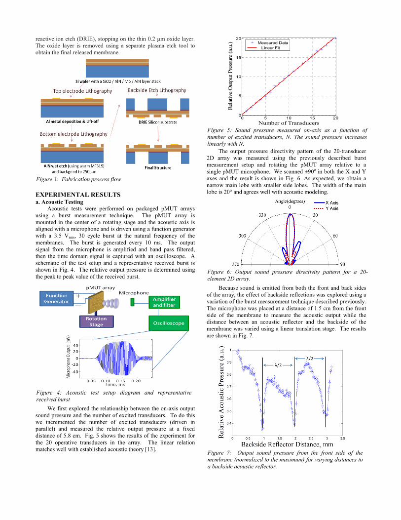
reactive ion etch (DRIE), stopping on the thin 0.2 µm oxide layer.
The oxide layer is removed using a separate plasma etch tool to
obtain the final released membrane.
EXPERIMENTAL RESULTS a. Acoustic Testing
Acoustic tests were performed on packaged pMUT arrays
using a burst measurement technique. The pMUT array is
mounted in the center of a rotating stage and the acoustic axis is
aligned with a microphone and is driven using a function generator
with a 3.5 Vrms, 30 cycle burst at the natural frequency of the
membranes. The burst is generated every 10 ms. The output
signal from the microphone is amplified and band pass filtered,
then the time domain signal is captured with an oscilloscope. A
schematic of the test setup and a representative received burst is
shown in Fig. 4. The relative output pressure is determined using
the peak to peak value of the received burst.
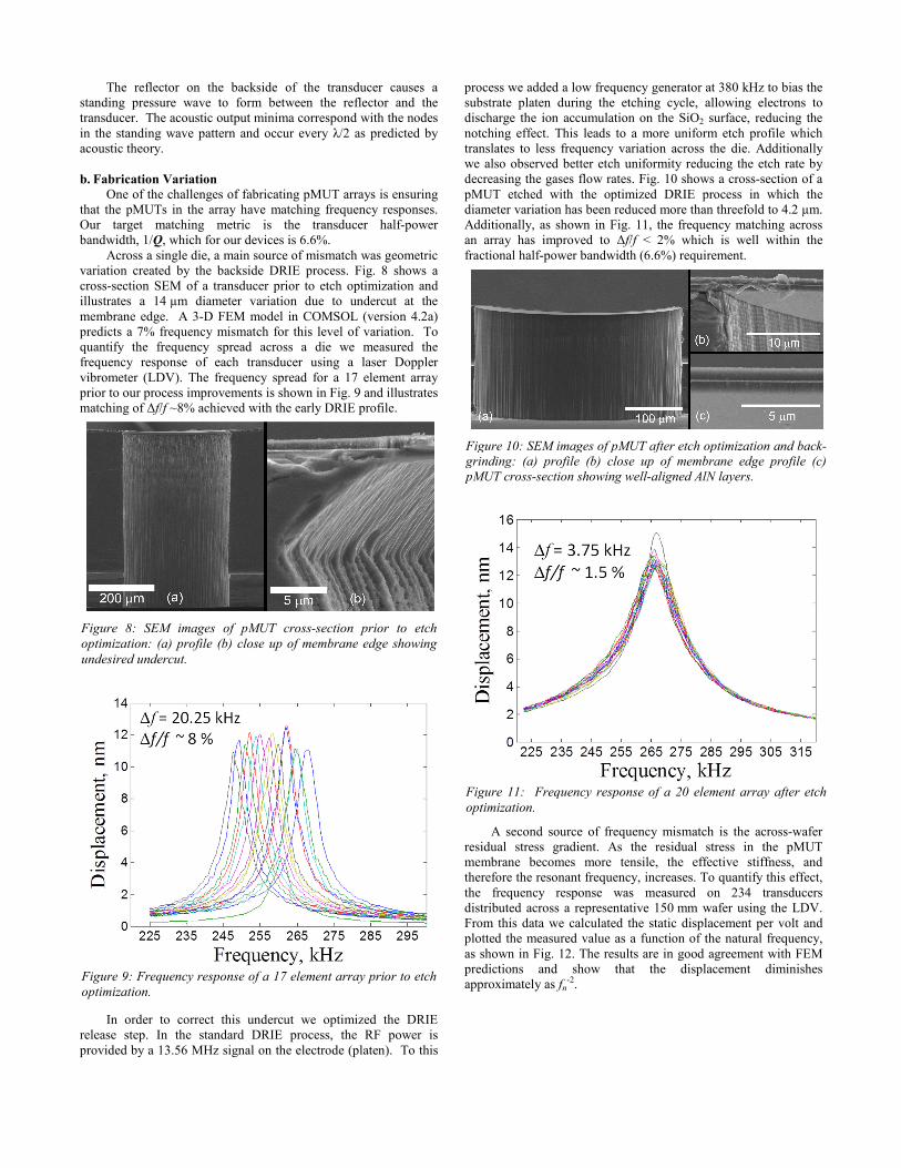
We first explored the relationship between the on-axis output
sound pressure and the number of excited transducers. To do this
we incremented the number of excited transducers (driven in
parallel) and measured the relative output pressure at a fixed
distance of 5.8 cm. Fig. 5 shows the results of the experiment for
the 20 operative transducers in the array. The linear relation
matches well with established acoustic theory [13].
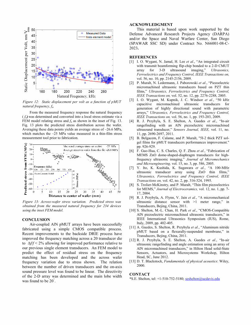
The output pressure directivity pattern of the 20-transducer
2D array was measured using the previously described burst
measurement setup and rotating the pMUT array relative to a
single pMUT microphone. We scanned ±90o in both the X and Y
axes and the result is shown in Fig. 6. As expected, we obtain a
narrow main lobe with smaller side lobes. The width of the main
lobe is 20° and agrees well with acoustic modeling.
Because sound is emitted from both the front and back sides
of the array, the effect of backside reflections was explored using a
variation of the burst measurement technique described previously.
The microphone was placed at a distance of 1.5 cm from the front
side of the membrane to measure the acoustic output while the
distance between an acoustic reflector and the backside of the
membrane was varied using a linear translation stage. The results
are shown in Fig. 7.
Figure 7: Output sound pressure from the front side of the
membrane (normalized to the maximum) for varying distances to
a backside acoustic reflector.
Figure 6: Output sound pressure directivity pattern for a 20-
element 2D array.
Figure 5: Sound pressure measured on-axis as a function of
number of excited transducers, N. The sound pressure increases
linearly with N.
0 5 10 15 200
5
10
15
20
Number of Transducers
Rel
ativ
e O
utp
ut Pre
ssure
(a.
u.)
Measured Data
Linear Fit
Figure 4: Acoustic test setup diagram and representative
received burst
Figure 3: Fabrication process flow
The reflector on the backside of the transducer causes a
standing pressure wave to form between the reflector and the
transducer. The acoustic output minima correspond with the nodes
in the standing wave pattern and occur every λ/2 as predicted by
acoustic theory.
b. Fabrication Variation
One of the challenges of fabricating pMUT arrays is ensuring
that the pMUTs in the array have matching frequency responses.
Our target matching metric is the transducer half-power
bandwidth, 1/Q, which for our devices is 6.6%.
Across a single die, a main source of mismatch was geometric
variation created by the backside DRIE process. Fig. 8 shows a
cross-section SEM of a transducer prior to etch optimization and
illustrates a 14 µm diameter variation due to undercut at the
membrane edge. A 3-D FEM model in COMSOL (version 4.2a)
predicts a 7% frequency mismatch for this level of variation. To
quantify the frequency spread across a die we measured the
frequency response of each transducer using a laser Doppler
vibrometer (LDV). The frequency spread for a 17 element array
prior to our process improvements is shown in Fig. 9 and illustrates
matching of ∆f/f ~8% achieved with the early DRIE profile.
In order to correct this undercut we optimized the DRIE
release step. In the standard DRIE process, the RF power is
provided by a 13.56 MHz signal on the electrode (platen). To this
process we added a low frequency generator at 380 kHz to bias the
substrate platen during the etching cycle, allowing electrons to
discharge the ion accumulation on the SiO2 surface, reducing the
notching effect. This leads to a more uniform etch profile which
translates to less frequency variation across the die. Additionally
we also observed better etch uniformity reducing the etch rate by
decreasing the gases flow rates. Fig. 10 shows a cross-section of a
pMUT etched with the optimized DRIE process in which the
diameter variation has been reduced more than threefold to 4.2 µm.
Additionally, as shown in Fig. 11, the frequency matching across
an array has improved to ∆f/f < 2% which is well within the
fractional half-power bandwidth (6.6%) requirement.
A second source of frequency mismatch is the across-wafer
residual stress gradient. As the residual stress in the pMUT
membrane becomes more tensile, the effective stiffness, and
therefore the resonant frequency, increases. To quantify this effect,
the frequency response was measured on 234 transducers
distributed across a representative 150 mm wafer using the LDV.
From this data we calculated the static displacement per volt and
plotted the measured value as a function of the natural frequency,
as shown in Fig. 12. The results are in good agreement with FEM
predictions and show that the displacement diminishes
approximately as fn-2.
Figure 11: Frequency response of a 20 element array after etch
optimization.
Figure 10: SEM images of pMUT after etch optimization and back-
grinding: (a) profile (b) close up of membrane edge profile (c)
pMUT cross-section showing well-aligned AlN layers.
Figure 9: Frequency response of a 17 element array prior to etch
optimization.
Figure 8: SEM images of pMUT cross-section prior to etch
optimization: (a) profile (b) close up of membrane edge showing
undesired undercut.
From the measured frequency response the natural frequency
( fn) was determined and converted into a local stress estimate via a
FEM model relating stress and fn as shown in the inset of Fig. 13.
Fig. 13 plots the predicted stress distribution across the wafer.
Averaging these data points yields an average stress of –26.6 MPa,
which matches the –25 MPa value measured in a thin-film stress
measurement tool prior to fabrication.
CONCLUSION
Air-coupled AlN pMUT arrays have been successfully
fabricated using a simple CMOS compatible process.
Recent improvements to the backside DRIE process have
improved the frequency matching across a 20 transducer die
to ∆f/f < 2% allowing for improved performance relative to
our previous single element transducers. An FEM model to
predict the effect of residual stress on the frequency
matching has been developed and the across wafer
frequency variation due to stress shown. The relation
between the number of driven transducers and the on-axis
sound pressure level was found to be linear. The directivity
of the 2-D array was determined and the main lobe width
was found to be 20°.
ACKNOWLEDGMENT
This material is based upon work supported by the
Defense Advanced Research Projects Agency (DARPA)
and/or the Space and Naval Warfare Center, San Diego
(SPAWAR SSC SD) under Contract No. N66001-08-C-
2023.
REFERENCES [1] I. O. Wygant, N. Jamal, H. Lee et al., “An integrated circuit
with transmit beamforming flip-chip bonded to a 2-D CMUT
array for 3-D ultrasound imaging,” Ultrasonics,
Ferroelectrics and Frequency Control, IEEE Transactions on,
vol. 56, no. 10, pp. 2145-2156, 2009.
[2] P. Muralt, N. Ledermann, J. Paborowski et al., “Piezoelectric
micromachined ultrasonic transducers based on PZT thin
films,” Ultrasonics, Ferroelectrics and Frequency Control,
IEEE Transactions on, vol. 52, no. 12, pp. 2276-2288, 2005.
[3] I. O. Wygant, M. Kupnik, J. C. Windsor et al., “50 kHz
capacitive micromachined ultrasonic transducers for
generation of highly directional sound with parametric
arrays,” Ultrasonics, Ferroelectrics and Frequency Control,
IEEE Transactions on, vol. 56, no. 1, pp. 193-203, 2009.
[4] R. J. Przybyla, S. E. Shelton, A. Guedes et al., “In-air
rangefinding with an AlN piezoelectric micromachined
ultrasound transducer,” Sensors Journal, IEEE, vol. 11, no.
11, pp. 2690-2697, 2011.
[5] B. Belgacem, F. Calame, and P. Muralt, "5I-2 thick PZT sol-
gel films for pMUT transducers performances improvement."
pp. 926-929.
[6] F. Guo-Hua, C. S. Charles, Q. F. Zhou et al., “Fabrication of
MEMS ZnO dome-shaped-diaphragm transducers for high-
frequency ultrasonic imaging,” Journal of Micromechanics
and Microengineering, vol. 15, no. 3, pp. 586, 2005.
[7] Y. Ito, K. Kushida, K. Sugawara et al., “A 100-MHz
ultrasonic transducer array using ZnO thin films,”
Ultrasonics, Ferroelectrics and Frequency Control, IEEE
Transactions on, vol. 42, no. 2, pp. 316-324, 1995.
[8] S. Trolier-McKinstry, and P. Muralt, “Thin film piezoelectrics
for MEMS,” Journal of Electroceramics, vol. 12, no. 1, pp. 7-
17, 2004.
[9] R. J. Przybyla, A. Flynn, V. Jain et al., “A micromechanical
ultrasonic distance sensor with >1 meter range,” in
Transducers, Bejing, China, 2011.
[10] S. Shelton, M.-L. Chan, H. Park et al., “CMOS-Compatible
AlN piezoelectric micromachined ultrasonic transducers,” in
IEEE International Ultrasonics Symposium (IUS), Rome,
Italy, 2009, pp. 402-405.
[11] A. Guedes, S. Shelton, R. Przybyla et al., “Aluminum nitride
pMUT based on a flexurally-suspended membrane,” in
Transducers, Bejing, China, 2011.
[12] R. J. Przybyla, S. E. Shelton, A. Guedes et al., “In-air
ultrasonic rangefinding and angle estimation using an array of
AlN micromachined transducers,” in Hilton Head solid-State
Sensors, Actuators, and Microsystems Workshop, Hilton
Head, SC, June 2012.
[13] D. T. Blackstock, Fundamentals of physical acoustics: Wiley,
2000.
CONTACT *S.E. Shelton, tel: +1-510-752-5180; [email protected]
Figure 13: Across-wafer stress variation. Predicted stress was
obtained from the measured natural frequency for 234 devices
using the inset FEM model.
Figure 12: Static displacement per volt as a function of pMUT
natural frequency, fn.


![· [Key words] aluminum nitride ( A IN) ; ceramic powder injection molding ( CIM) ; binder; debinding [ ac number] 484.5 1 INTRODUCTION Aluminum nitride ( A IN) , which has excellent](https://static.fdocuments.in/doc/165x107/605bedf6b259446f347a98da/key-words-aluminum-nitride-a-in-ceramic-powder-injection-molding-cim-.jpg)