AltiumLive 2017: ELECTROMAGNETIC FIELDS FOR NORMAL FOLKS · Designing Good Transmission Lines...
62
AltiumLive 2017: ELECTROMAGNETIC FIELDS FOR NORMAL FOLKS Daniel Beeker Principal Engineer San Diego, CA October 3 rd 2017
Transcript of AltiumLive 2017: ELECTROMAGNETIC FIELDS FOR NORMAL FOLKS · Designing Good Transmission Lines...

AltiumLive 2017:ELECTROMAGNETIC FIELDS FOR NORMAL FOLKS
Daniel BeekerPrincipal Engineer
San Diego, CAOctober 3rd
2017

Show Me the Pictures and Hold the Equations, Please!

Because You Know…
It’s All About the Space!(not wires)

Because you know it’s all about the space
'Bout the space, not wiresIt’s all about the space'Bout the space, not wiresIt’s all about the space'Bout the space, not wiresIt’s all about the space'Bout the space... space...
space... space
Yeah, it's pretty clear, you don’t believe it
But the wires just show, just show, where all the fields will fit
‘Cause all the energy only moves in the space
“Gotta put all the wires in all the right places”
I know your teacher said, it’s the conductor
We know that’s not the way, don’t listen to, the instructor
If you got fields a movin’, you got current flow
‘Cause it’s the movin’ fields that really make everything go
Yeah, your teachers they told you "don't worry about the field”
They said, “The math that they use isn’t something you wish to wield”.
You know that circuits are better, you just have to make them connect
So if that’s what you’re into, then you know what to expect
Because you know it’s all about the space
'Bout the space, not wiresIt’s all about the space'Bout the space, not wiresIt’s all about the space'Bout the space, not wiresIt’s all about the space'Bout the space... Hey!
I'm bringing physics backGo 'head and tell them
circuit fossils thatNo, I'm just saying, I know
you think they're rightBut I'm here to tell you...Physics tells us that it fields
in space that’s really outta sight
I know your teacher said, it’s the conductor that holds the key
We know that’s not the way, you’ve gotta listen to me
If you got fields that are movin’, that makes all the current flow
So you gotta take all of this in, and lose all that you know
Because you know it’s all about the space
'Bout the space, not wiresIt’s all about the space'Bout the space, not wiresIt’s all about the space'Bout the space, not wiresIt’s all about the space'Bout the space...
In Case You Already Forgot…“All About the Space“ To the tune of Meghan Trainor’s “All about that Bass”. Copyright 2015 Daniel L. Beeker. http://youtu.be/WglPHiZx4Gw
Page 4

Foundation of Electronics
1
What’s in the Waves
Designing Good Transmission Lines
Changes on the Wind
Electromagnetic Field Behaviour
2
3
4
5
Agenda
Closing Remarks6
Page 5

What Changes?
• Smaller device geometries and higher current switching capabilities have
thrust us all into the world of RF, HF, UHF and microwave energy
management.
• Rise times on even the lowest tech devices now exhibit gigahertz impact.
• These changes directly impact product functionality and reliability.
Page 6

IC technology was described as % shrink from Integer Design Rules
• Circuit-based approach usually was close enough
IC technology now described in nanometers
• Circuit-based approach completely falls apart
EM field (physics) based approach essential
• EMC standards have changed• Lower frequency compliance requirements
• Higher frequency compliance requirements
• Lower emission levels allowed
• Greater immunity required
The playing field and the equipment have changed!
This really is a brand new game!
What Changes?
Page 7

What Can We Do?
•The skills required are only taught in a few universities
•Missouri University of Science and Technology (formerly the University of Missouri-
Rolla)
http://www.mst.edu/
•Clemson University
http://www.cvel.clemson.edu/emc
•Our sagest mentors may not be able to help
•Nearly every rule of thumb is wrong
•To gain the skills needed, you have to actively seek them
•Industry conferences
• Altium Live 2017
• PCB West
• IEEE EMC Society events Page 8

What Can We Do?
Page 9
About Me: Daniel Beeker
• 37+ years experience at Motorola/Freescale/NXP designing and working with
microprocessor and microcontroller development systems
• 30+ years working with automotive customers in one of the most demanding
embedded control environments
• Championing the cause for increased awareness of advanced design
technologies
• Used to believe in black magic, but Ralph Morrison set me straight!
• Firmly entrenched in physics-based design philosophy

What’s in the Waves
Designing Good Transmission Lines
Changes on the Wind
Electromagnetic Field Behaviour3
4
5
Agenda
2
1
Foundation of Electronics
Closing Remarks6
Page 10
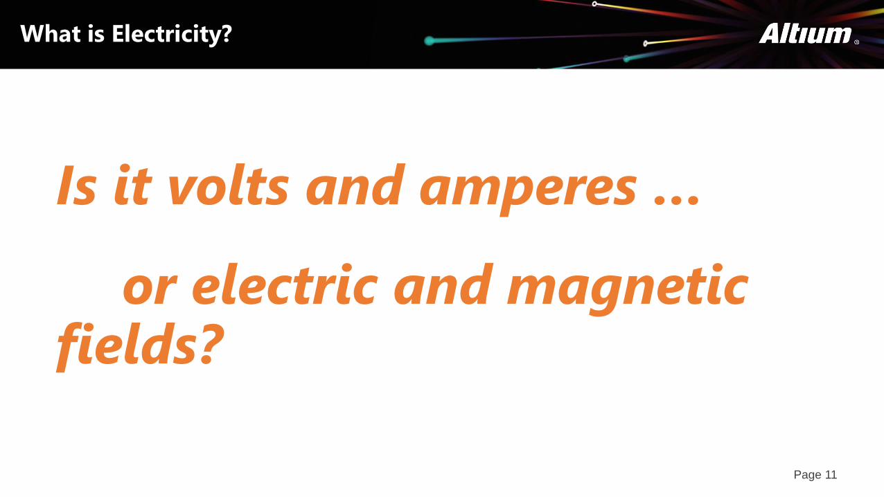
What is Electricity?
Is it volts and amperes …
or electric and magnetic fields?
Page 11

• Fields are basic to all circuit operation
• Volts and amperes make things practical
• We easily can measure volts and amperes
• More difficult to measure “E” and “H” fields
• In high clock rate (and rise time) circuits, once the "quasi static”
approximation does not hold true anymore, field control plays a
critical role
• This must be a carefully considered part of any design
(Slide compliments of Ralph Morrison, Consultant)
What is Electricity?
Page 12

Maxwell’s Equations
(Slide compliments of http://www.physics.udel.edu/~watson/phys208/ending2.html)
Page 13

Maxwell’s Equations
Page 14
Maxwell was smart!

Heresy!!
•Maxwell’s equations are all about the interaction between electric and magnetic fields
•There are not any electrons in them• No holes, either
• If it were all about electrons moving, how would fields move through space???
Page 15

News Flash!
• We all are involved with developing products which generate, control and
consume ELECTROMAGNETIC FIELD ENERY• This is not what we are taught.
• Circuit theory pretends that electric energy is made up of electrons moving in the
conductors
• Switches add conductors, and the current instantly starts to move in the loop. The wires
carry the energy, and the load instantly affects the flow of energy.
• WRONG!!• Switches add new spaces, and the moving field carries the energy.
• It takes time for the field energy to move into that space. The moving field energy has no
idea of what it is at the end of the new space.
• Field energy moving through a space induces current flow in the conductors. The magic
here is the displacement current flowing through the dielectric at the wave front, completing
the circuit.
Page 16

What is Electricity?
Page 17
Fields do all of the work
• “Current flow” is caused by moving field energy
• “Current flow” is an artifact caused by moving fields, in the conductors that bound them
• This is a result of the fields interacting with the molecules in the conductor
• This interaction consumes some of the field energy, hence a resulting voltage drop caused by
this “resistance”
• This consumption of field energy results in increased movement of the molecules, hence is
converted to “heat”!
• The dielectric also consumes energy the same way, unless it is a vacuum.
• Electromagnetic energy moves slower through a physical dielectric that through space for the
same reason
• It takes TIME for the interaction between the molecules in the dielectric, even in air.
• The field has to stop and shake hands with every molecule it meets!

• THAT is NOT what WE were taught.
• THAT is NOT the perspective we have used our entire careers.
• How dare you contradict my professors and my mentors?
• Didn’t what we are doing work for years?
• Don’t I just have to connect the pins and things will work?
• …Wait a minute, then why do we have so much trouble with signal
integrity and EMC??
• Maybe there IS something we are missing…
Heresy!!
Page 18

What’s in the Waves
Designing Good Transmission Lines
Changes on the Wind
4
5
Agenda
1
Foundation of Electronics 2
3 Electromagnetic Field Behavior
Closing Remarks6
Page 19

Myths We Depended On
• Fields are invisible
• Fields are well behaved
• Fields follow the trace
• Fields avoid open spaces
• Fields are someone else’s problem
• Fields are only important in RF and power supply designs
• Fields are only for farmers
Page 20
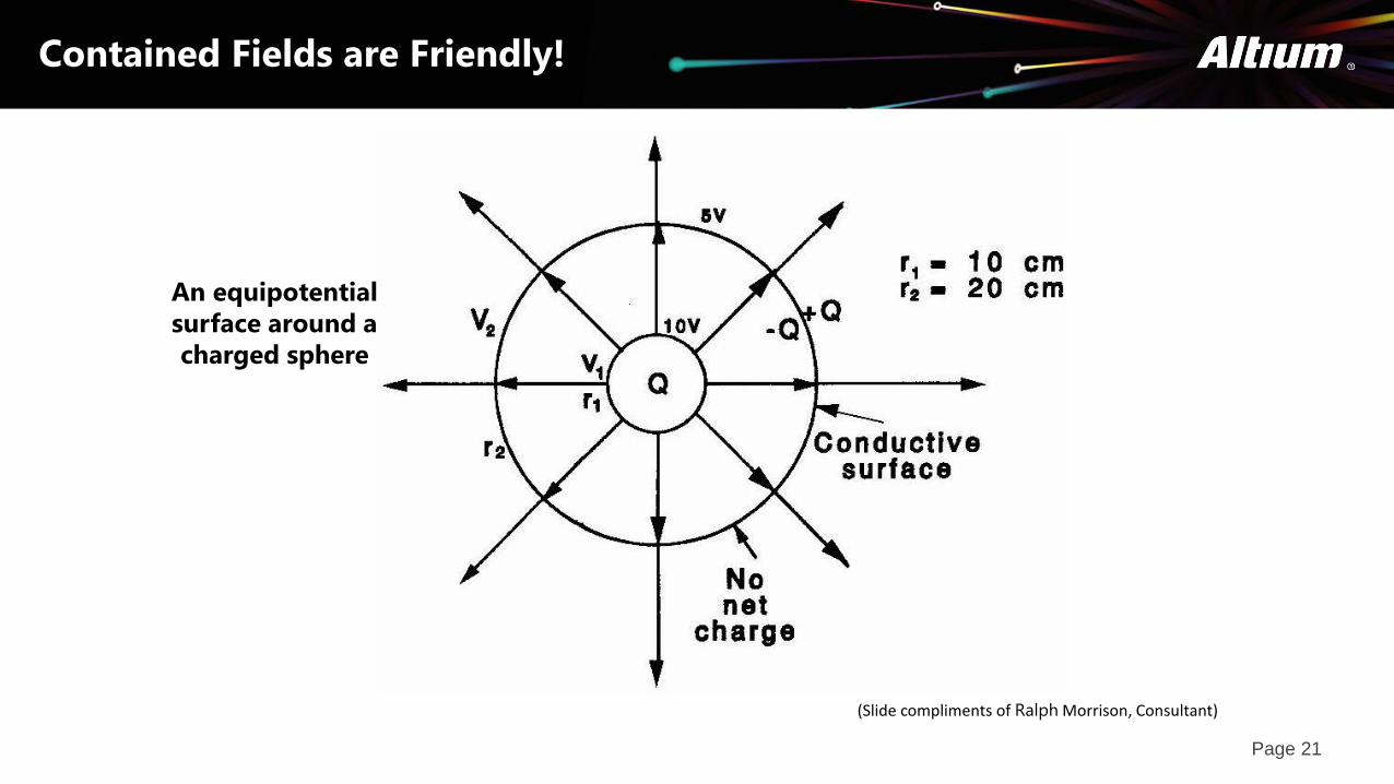
Contained Fields are Friendly!
An equipotential
surface around a
charged sphere
(Slide compliments of Ralph Morrison, Consultant)
Page 21

A Loose Field is Not a Friendly Field
Field is not contained and looks for trouble(Slide compliments of Ralph Morrison, Consultant)
A shielded enclosure with an opening
Page 22

Contained Fields are Friendly!
Fields concentrate under the traces and there is little crosstalk.
Fields do not penetrate the plane(Slide compliments of Ralph Morrison, Consultant)
Page 23

Fields are Friendly!
A contained field is a friendly field:
• Happy field in a sphere
• Happy field in a good coaxial cable
• Happy field in a closely spaced transmission line pair
• Happy field between two closely spaced PCB planes
Page 24

Electromagnetic Field Behaviour
Designing Good Transmission Lines
Changes on the Wind
3
5
Agenda
1
Foundation of Electronics 2
4 What’s in the Waves
Closing Remarks6
Page 25
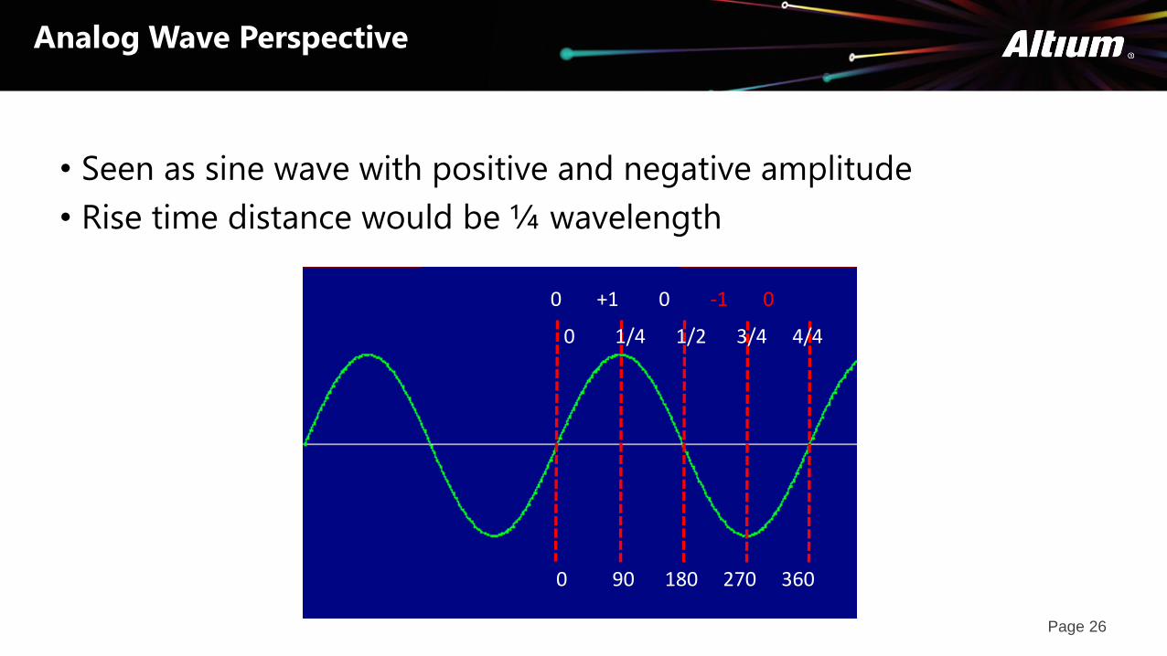
Analog Wave Perspective
• Seen as sine wave with positive and negative amplitude
• Rise time distance would be ¼ wavelength
0 +1 0 -1 0
0 90 180 270 360
0 1/4 1/2 3/4 4/4
Page 26

Antenna Size vs. Frequency
Frequency ¼ wave length
10 MHz HMOS
Rise time equivalent, 100 nanoseconds rise time distance, 100 feet
24.6 feet
Across the room
100 MHz (TTL Logic) UDR HCMOS
Rise time equivalent, 10 nanoseconds rise time distance, 10 feet
2.46 feet
Less than a yard
1 GHz (BiCMOS Logic) IDR HCMOS
Rise time equivalent, 1 nanosecond rise time distance, 1 foot
0.246 feet (2.952 inches)
Less than your finger
10 GHz (GaAs Logic) 65 nm HCMOS
Rise time equivalent, 100 picoseconds rise time distance, 1.2 inches
0.0246 feet (0.2952 inches)
Less than the diameter of a pencil
100 GHz 32 nm HCMOS
Rise time equivalent, 10 picoseconds rise time distance, 0.12 inches
0.00246 feet (0.0295 inches)
Half the thickness of a standard FR4 PCB
¼ wavelength is accepted as a good antenna size
In the Analog Domain, this is 90 degrees
Page 27

Antenna Size vs. Frequency
From the previous table, a few things become apparent:
• We got away with ignoring basic physics because IC switching speeds were slow and
efficient antennas had to be huge.
• At a switching speed of 1 nanosecond, it only takes a PCB feature (trace or slot) of 3 inches
to be an efficient antenna (1/4 wave length).
• Once you cross that magic boundary of 1 nanosecond, most PCB designs are capable of
providing a wonderful source of antennas.
• At 10 picosecond speeds, every structure in the system can be an good antenna.
Since TTL days:
Four order magnitude change in switching speeds
Almost no changes in PCB or system design philosophy
Page 28
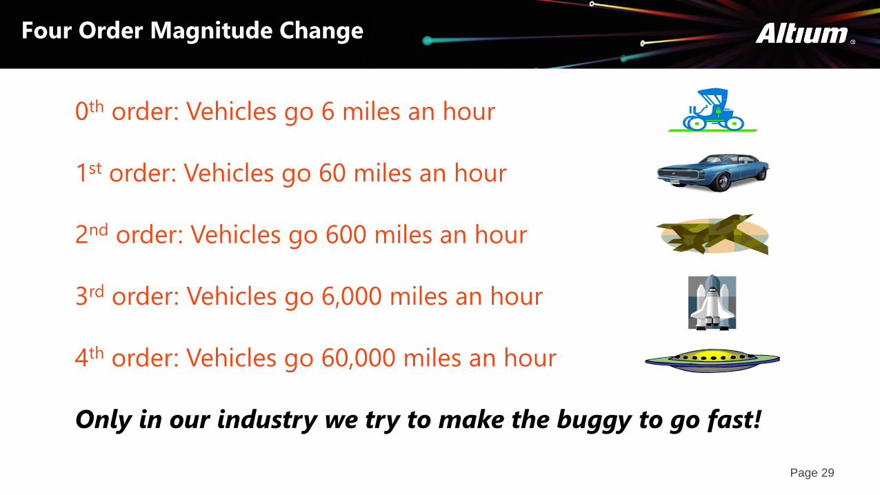
Four Order Magnitude Change
0th order: Vehicles go 6 miles an hour
1st order: Vehicles go 60 miles an hour
2nd order: Vehicles go 600 miles an hour
3rd order: Vehicles go 6,000 miles an hour
4th order: Vehicles go 60,000 miles an hour
Only in our industry we try to make the buggy to go fast!
Page 29

Electromagnetic Field Behaviour
What’s in the Waves
Changes on the Wind
3
4
Agenda
1
Foundation of Electronics 2
5 Designing Good Transmission Lines
Closing Remarks6
Page 30

Energy Management
Why does field energy follow conductors?• Why does water flow in a stream?
• Same reason
• Nature follows the path that stores the least energy
• It is easier for fields to follow traces than to go out across
space
The Impedance of free space is 377 ohms• Between conductor pairs it will be lower, so they follow the
path of lowest impedance (smallest volume)(Slide compliments of Ralph Morrison, Consultant)
Page 31

Energy Management
Transmission lines are convenient paths for energy
flow:
• Every conductor pair is a transmission line
• Trace-to-trace or trace-to-conducting plane
• The fields, and thus the energy flow, will concentrate
• between traces
• between a trace and a conducting plane
• Draw the fields to locate the current
(Slide compliments of Ralph Morrison, Consultant)
Page 32

The NEW (old) Reality
The Rule of Triplets
You only get 3 components to use to build electronic systems
• Conductors
• Spaces (dielectric)
• Switches
You can only do 3 things with Electromagnetic Field Energy
• Store it
• Move it
• Convert it to kinetic energy
This is not rocket science!Page 33

The NEW (old) Reality
We are all just plumbers!!
Using very leaky water pipes!!
We design three dimensional spaces for managing
EM field movement
Page 34
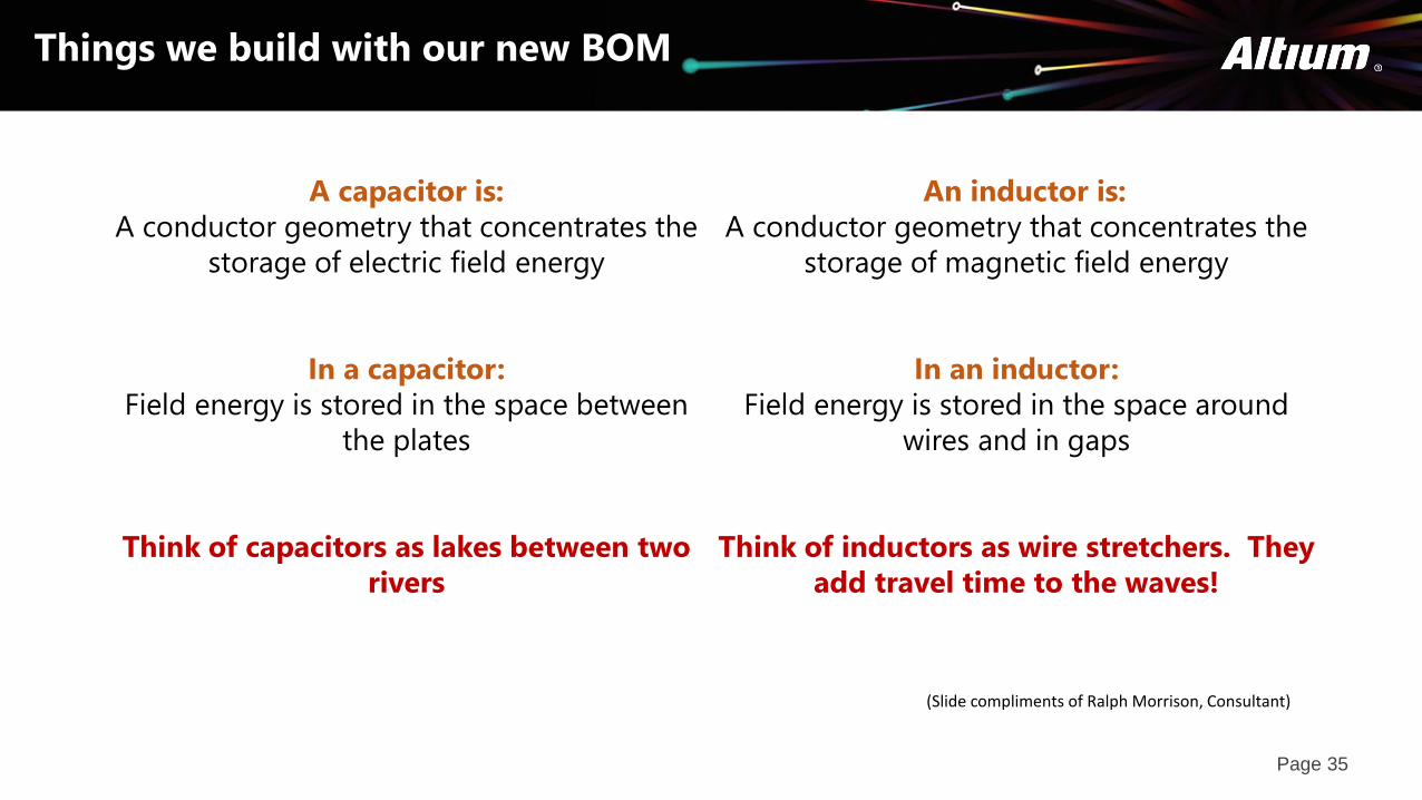
Things we build with our new BOM
A capacitor is:
A conductor geometry that concentrates the
storage of electric field energy
In a capacitor:
Field energy is stored in the space between
the plates
Think of capacitors as lakes between two
rivers
An inductor is:
A conductor geometry that concentrates the
storage of magnetic field energy
In an inductor:
Field energy is stored in the space around
wires and in gaps
Think of inductors as wire stretchers. They
add travel time to the waves!
(Slide compliments of Ralph Morrison, Consultant)
Page 35
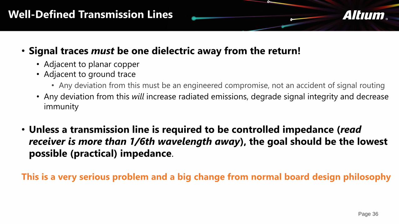
Well-Defined Transmission Lines
• Signal traces must be one dielectric away from the return!
• Adjacent to planar copper
• Adjacent to ground trace
• Any deviation from this must be an engineered compromise, not an accident of signal routing
• Any deviation from this will increase radiated emissions, degrade signal integrity and decrease
immunity
• Unless a transmission line is required to be controlled impedance (read
receiver is more than 1/6th wavelength away), the goal should be the lowest
possible (practical) impedance.
This is a very serious problem and a big change from normal board design philosophy
Page 36

Wave Reflection
Reflection Coefficient
Reflection:
• When Z2 = Z1 then = 0 or no reflection
• When Z2 > Z1 then > 0 or a plus reflection
• When Z2 < Z1 then < 0 or a negative reflection
=
Z2 – Z1
Z2 + Z1
(Slide compliments of Ralph Morrison, Consultant)
Page 37

Wave on a Transmission Line
Low impedance source to high impedance load
Wave reflects and voltage doubles
V
A B
5VV
V
5V
(Slide compliments of Ralph Morrison, Consultant)
Page 38

V
V
V
V
2x V
2x V
A B
Second Reflection at Source
From a low impedance to a high impedance, the wave voltage is doubled and reflected. From a high impedance to a low impedance, the wave voltage is inverted and reflected.
This is called “ringing” and continues until all of the energy is either transferred to the receiver, converted to heat in the dielectric, or radiates.
(Slide compliments of Ralph Morrison, Consultant)
Page 39

Impedance for Dummies
• Low impedance to a High impedance is like throwing a bucket
of water out of a small hole in the wall
• Most of the water splashes back at you
• High impedance to a Low impedance is like throwing a bucket
of water out of an open window
• It all goes out
Page 40

Well-Defined Transmission Lines
• Good news is that any discontinuity that is less than 1/6th wavelength
is virtually invisible to the signal
• Routing schemes need to be driven by the transistor geometry
• Any failure to insure that both signal and ground copper are
continuous (and adjacent) will result in large discontinuities that will
cause signal integrity and EMC issues
• Vertical transitions can not be not excluded
• This is the most common mistake made in otherwise good designs
Page 41

Rise Time Distance
Now, what does this really mean?• Rise time distance is how far the wave travels by the time it reaches full amplitude.
• Determined by the switching speed of the output driver
• In digital circuits, this is really ½ wavelength, or 180 degrees!
Let’s look at this from a switching speed vs. lumped distance perspective. • Lumped distances are basically the size of a discontinuity which remains invisible to the energy flow.
• To prevent problems on uncontrolled impedance transmission lines, the load must be less than 1/6 of
the wavelength (67% amplitude reflection)
• The voltage developed is less than ½ of the output voltage, so the reflection is less than the output
voltage
• One reflection and the transmission line is stable
How far is that for a given switching speed?
Page 42

Digital Wave Perspective
• Square wave is made up of an infinite number of frequencies
• Design for the highest frequency the driver is capable of supporting
Page 43
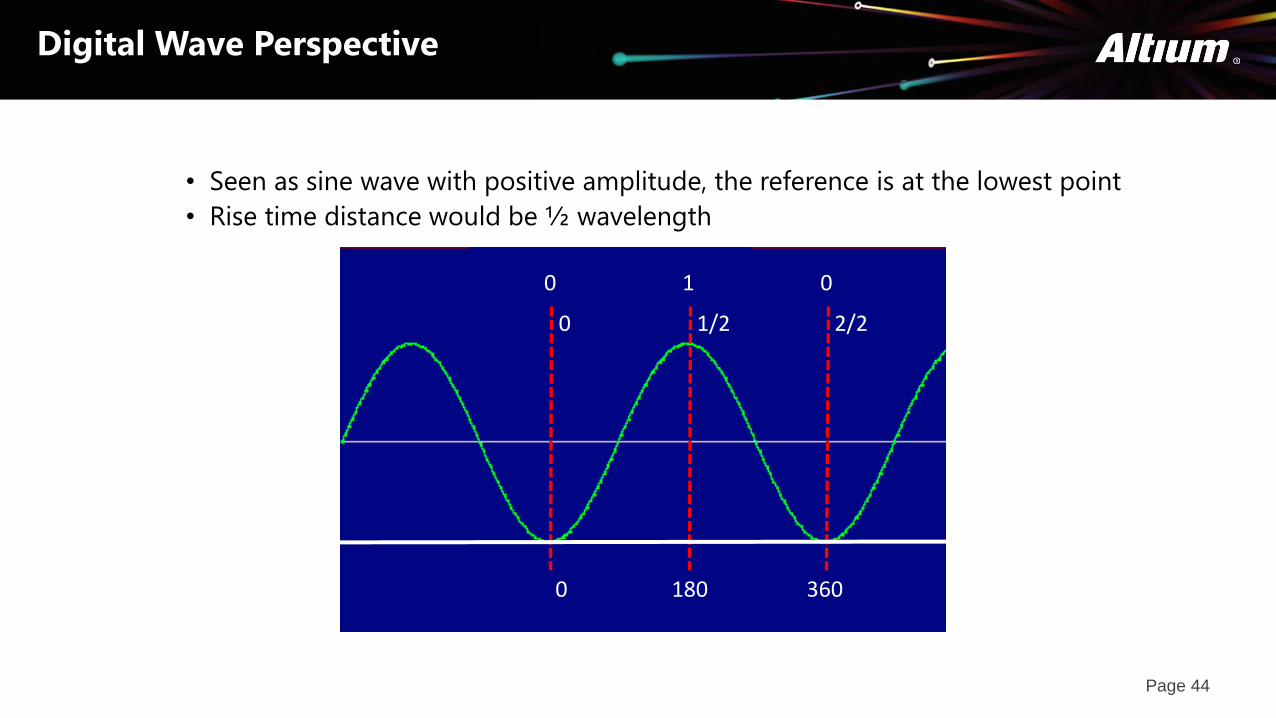
Digital Wave Perspective
• Seen as sine wave with positive amplitude, the reference is at the lowest point
• Rise time distance would be ½ wavelength
0 1 0
0 180 360
0 1/2 2/2
Page 44

Switching Frequency vs. Lumped Distance (Inner Layer)
Rise time distance is ½ wavelength in digital domain, or 180 degrees
Frequency 1/6 wave length
5 MHz HMOS
Rise time equivalent, 100 nanoseconds Rise time distance, 100 feet
16.4 feet
In the room
50 MHz (TTL Logic) UDR HCMOS
Rise time equivalent, 10 nanoseconds Rise time distance, 10 feet
1.64 feet
Anywhere on the board
500 MHz (BiCMOS Logic) IDR HCMOS
Rise time equivalent, 1 nanosecond Rise time distance, 1 foot
0.164 feet (1.968 inches)
Pretty close
5 GHz (GaAs Logic) 65 nm HCMOS
Rise time equivalent, 100 picoseconds Rise time distance, 1.2 inches
0.0164 feet (0.1968 inches)
In the package
50 GHz 32 nm HCMOS
Rise time equivalent, 10 picoseconds Rise time distance, 0.12 inches
0.00164 feet (0.01968 in. or 500 µm)
On the die
Page 45

Transmission Line Properties
In a good design:
• Energy is available whenever there is a demand
• The voltage source must be reasonably constant
• Energy must be replaced after it is used or there will be logic (signal integrity)
problems
• This is called energy management
Local sources of energy:
• Decoupling capacitors
• There is also energy available from ground/power plane capacitance
New problem:
• It takes time to move this energy from storage to a load(Slide compliments of Ralph Morrison, Consultant)
Page 46

Energy Delivery From A Storage Device
• For energy to be delivered from a storage device:
• The wave requesting the energy (seen as a drop in the power supply voltage
caused by the switching event) has to travel to the source and back to the
switch
• It’s a two-way trip!
Page 47

Fields are Friendly!
Fields need to be carefully managed:
• Every connection must be treated as part of a transmission line pair• Field volumes (read transmission line impedance) must be carefully
managed• Each discontinuity (read change in transmission line GEOMETRY) results
in reflections• Each segment of this geometry must have enough field energy
delivered to match the field density (read voltage) from the driver
• This all takes TIME
• Yes, this is now a four-dimensional geometric design problem
Page 48

How Long Does It Take?
Wave velocity
• For traces on a circuit board v = c / € 1/2
• Where c is the velocity of light and € is the relative dielectric constant
• v = 150 mm / ns or 6” / ns
All energy is moved by wave action!
• A drop in voltage sends a wave to get more energy
• Waves reflect at discontinuities
• A source of voltage is a discontinuity
• Each reflected wave can carry a limited amount of energy
(Slide compliments of Ralph Morrison, Consultant)
Page 49

Getting 1 Ampere to Flow
What does this mean in my circuit board?
• Initial power level in a 50 Ohm line (bucket size)• 5 Ohm load and 5 V source
• I = 0.1 amperes or ½ watt
• Remember, Amperes are really Coulombs of charge moving per second, FIELD ENERGY!
Now, how do I get 1 ampere?
• Even if the line is only 1/16 inch long:• It takes 10 ps for a wave to go 1/16 inch in FR4
• It takes 20 ps for a wave to make one round trip
• It takes 30 round trips on that line to bring current level up to near one amp
• That is 600 ps, assuming zero rise time
(Slide compliments of Ralph Morrison, Consultant)
Page 50

Getting 1 Ampere to Flow
Note: This is not a curve, but a series of step functions. The amplitude of the step is determined by the impedance of the transmission line and the width of the step is determined by the length of the transmission line and a two way transition for the wave.
(Slide compliments of Ralph Morrison, Consultant)
Page 51

Typical 1/16 Inch Connections
• Traces to capacitors
• Connections to IC dies• Lead frames and wire bonds
• BGA interposers
• Traces to vias
• Vias to ground/power planes
• Remember, 1/16 inch is about 10 pS
• Yes, you do care about picoseconds now!
Page 52

Switching Frequency vs. Power Source
Frequency 1/20 wave length
5 MHz HMOS
Rise time equivalent, 100 nanoseconds Rise time distance, 100 feet
4.92 feet
Somewhere in the room
50 MHz (TTL Logic) UDR HCMOS
Rise time equivalent, 10 nanoseconds Rise time distance, 10 feet
.492 feet
Somewhere on the board, should be routed as co-planar pairs
500 MHz (BiCMOS Logic) IDR HCMOS
Rise time equivalent, 1 nanosecond Rise time distance, 1 foot
0.0492 feet (0.59 inches)
Width of your finger, time to look at small geometry capacitors and power islands
5 GHz (GaAs Logic) 65 nm HCMOS
Rise time equivalent, 100 picoseconds Rise time distance, 1.2 inches
0.00492 feet (0.059 in. or 1498.6 µm)
In the package
50 GHz 32 nm HCMOS
Rise time equivalent, 10 picoseconds Rise time distance, 0.12 inches
0.000492 feet (0.0059 in. or 149.86 µm)
On the die
Page 53

Energy Management
All energy is moved by wave action!
When a switching element closes, this results in a drop in the voltage on the power supply. The resulting
field energy request wave travels until this request is filled or it radiates. Depletion waves are the most
common source of EMC issues.
The only way to reduce noise in a system is to provide adequate
sources of Electromagnetic field energy.
The only ways to improve power delivery:
Move the storage device closer (less travel time)
Reduce the impedance of the transmission line (wider traces or thinner dielectrics, i.e. bigger buckets)
Add more connecting transmission lines (more buckets)
(Slide compliments of Ralph Morrison, Consultant)
Page 54

Energy source hierarchyEach can supply energy determined by the space it contains and the spaces (transmission lines) between the
elements
• On-chip capacitance − (10s of fs) - Closest, supports the highest frequencies
• Space between the wire bonds − (100s of fs) - Farther away, but still help to feed the on-chip capacitors
• Between layers of Substrate (BGA) or lead frame (QFP) − (1s of ps) - Farther still, feeds the wire bond spaces
• Power/ground plane pairs, if present – (10s of ps) - Power islands are best, used to collect the power pins and connect to the next element, feed the package
• Local bypass capacitors – (10s of ps) - Small geometry (usually 0402), placed as close as possible, feed the power islands or package
• Field energy stored across the PCB structure – (100s 0f ps) - Larger packages placed in the realm of the ICs, feed the local bypass devices
• Bulk storage capacitors – (10s of ns) - Near the voltage regulator, feed the regional capacitors
• Finally the power supply – (100s of ns) - Collects energy from the outside world and fills the bulk capacitors
Page 55
Energy Management

Switching Frequency vs. Power Source
• If the energy source is not inside the 1/20 wavelength distance, there will be radiated energy
caused by the switching event
• The job of the PCB designer is to minimize the amount of energy by managing the power delivery
system for each type of switching event
• As the geometry of the ICs we use continues to shrink, so does the area of effective power delivery
• Well-defined power delivery transmission lines and small geometry, low impedance field storage
devices are essential
• Even if they are outside of the “zone,” they can minimize the amount of radiated energy
We have to keep the field happy and contained as far up the food chain as we can, to reduce
system noise.
Page 56

Electromagnetic Field Behaviour
What’s in the Waves
Changes on the Wind
3
4
Agenda
1
Foundation of Electronics 2
Designing Good Transmission Lines5
6 Closing Remarks
Page 57

Fundamentals to Remember
• Electromagnetic fields travel in the space between the conductors, not in the conductors
• The switching speed of the transistors determines the frequency of operation, not the clock rate
• Signal and power connections need to be one dielectric from ground for their entire length (including layer transitions)• Adjacent plane
• Co-planar trace
• There is no such thing as a noisy ground, just poor transmission line design
• To quote Dr. Todd Hubing, “Thou shalt not split ground.”
• Any compromises to these rules will increase system noise and must be done as carefully considered engineering decisions
Page 58

Special Thanks to My Mentors
Rick Hartley PCB designer extraordinaire, started me down this trail in 2004 at PCB West
Ralph Morrison Author, inventor and musician, has patiently and steadily moved me from the fuzzy
realm of “circuit theory” and “black magic” into the solid world of physics
Dr. Todd Hubing Researcher, professor and consultant, whose research at UMR and Clemson has
provided solid evidence that Maxwell and Ralph have got it right!
Page 59

It’s All About the Space!!
“Buildings have walls and halls. People travel in the halls not the walls.
Circuits have traces and spaces. Energy and signals travel in the
spaces not the traces.”
- Ralph Morrison
Page 60

Summary
• Electromagnetic fields travel in the space between the conductors
• Movement of EM fields induces current flow in the conductors
• It is important to consider the time it takes for the EM fields to move
through the dielectric from the transmitter to the receiver
• Switching speed of the output devices determines the requirements of
the power supply and the transmission line design
• Well-defined transmission lines result in significantly improved EMC
performance
• The black magic is tamed!
Page 61

Thanks for your Attention!
Questions?