Alternating Current Loss Measurement of Power Cable ... · The electrical measurement method needs...
207
ALTERNATING CURRENT LOSS MEASUREMENT OF POWER CABLE CONDUCTORS WITH LARGE CROSS SECTIONS USING ELECTRICAL METHODS vorgelegt von Master of Science René Suchantke geboren in Berlin von der Fakultät IV - Elektrotechnik und Informatik der Technischen Universität Berlin zur Erlangung des akademischen Grades Doktor der Ingenieurwissenschaften - Dr.-Ing. - genehmigte Dissertation Promotionsausschuss: Vorsitzender: Prof. Dr.-Ing. Kai Strunz Gutachter: Prof. Dr.-Ing. Ronald Plath Gutachter: Prof. Dr.-Ing. Steffen Großmann Gutachter: Prof. Dr.-Ing. Rolf Schuhmann Tag der wissenschaftlichen Aussprache: 13. Juli 2018 Berlin 2018
Transcript of Alternating Current Loss Measurement of Power Cable ... · The electrical measurement method needs...

A LT E R N AT I N G C U R R E N T L O S S M E A S U R E M E N T O F P O W E RC A B L E C O N D U C T O R S W I T H L A R G E C R O S S S E C T I O N S U S I N G
E L E C T R I C A L M E T H O D S
vorgelegt vonMaster of ScienceRené Suchantke
geboren in Berlin
von der Fakultät IV - Elektrotechnik und Informatikder Technischen Universität Berlin
zur Erlangung des akademischen Grades
Doktor der Ingenieurwissenschaften- Dr.-Ing. -
genehmigte Dissertation
Promotionsausschuss:Vorsitzender: Prof. Dr.-Ing. Kai StrunzGutachter: Prof. Dr.-Ing. Ronald PlathGutachter: Prof. Dr.-Ing. Steffen GroßmannGutachter: Prof. Dr.-Ing. Rolf Schuhmann
Tag der wissenschaftlichen Aussprache: 13. Juli 2018
Berlin 2018

René Suchantke: Alternating Current Loss Measurement of Power Cable Conduc-tors with Large Cross Sections Using Electrical Methods © July 2018

Dedicated to my beloved wife and biggest critic Isabell.
You, the people, have the power,the power to create machines,
the power to create happiness!You, the people, have the power
to make this life free and beautiful,to make this life a wonderful adventure. [...]
Let us fight for a world of reason,a world where science and progress
will lead to all men’s happiness.
Charlie Chaplin


A B S T R A C T
High voltage power cables for bulk AC power transport use the Millikenconductor design from a certain cross section up to decrease transmissionlosses. It is not possible to reliably assess their AC losses by simulation orother calculation methods in advance, as the performance of this complexdesign strongly depends on manufacturing processes and quality. The exactknowledge of the AC resistance is important, because it is a critical designparameter for the thermal dimensioning of the cable and whole cablesystems. Therefore, it is necessary to accurately determine the AC lossesby measurement using the electrical or the calorimetric method. This workfocuses on the electrical method solely, as it can be performed much fasterwith less logistical effort. The goal is to have a measurement setup, wherethe measured losses are as close as possible to the true losses. The true lossesresult in conductor heating, which limits the transmission power. They arealso called Joule losses.
Theoretical calculations, FEM simulations in Comsol Multiphysics and mea-surements have been used in combination to evaluate different, possibleinfluences in AC resistance measurements. After the problem definitionand the presentation of the methodology, past advances and conceptsfocusing on AC resistance determination were shown. Then, after thebasics were made clear to the reader, the measurement circuit was definedand different error sources in measurement setups were evaluated. Theseincluded the influence of the sheath and return conductor position upontrue and measured losses, the influence of current homogenization andplacement of voltage tap-offs. A recommendation for the preparation, setupand measurement procedure was given. At the end, multiple Millikenconductors were measured using the proposed method and compared tothe IEC standard.
It was shown that the electrical measurement method is able to measurethe true AC losses of complex conductors consisting of insulated wires. Oneimportant requirement is that the voltage pick-up loop is large enough tocapture enough complex magnetic field originating from the conductorunder test. On the other side, complex magnetic fields caused by eddycurrents in adjacent conductors should not be captured by the pick-uploop as they also affect the measured losses. Using 2 equally spaced returnconductors in the same plane as the conductor under test and the averageof at least 4 evenly distributed voltage pick-up loops located at the surfaceof the insulation of the cable, will deliver results of sufficient accuracy.
The findings of this thesis indicate that great care must be taken for multipleaspects in the AC resistance measurement of complex conductors. Engineersperforming AC resistance measurements have to be aware of error sources,specifically the interplay between conductor positions and apparent losses.The electrical measurement method needs to be thoroughly prepared, espe-cially regarding the contacting of current path and voltage tap-offs. Never-theless, the effort concerning time and logistics is still significantly smallercompared to a calorimetric measurement.

Z U S A M M E N FA S S U N G
Hochspannungskabel für die Übertragung großer Mengen elektrischerEnergie verwenden ab einem bestimmten Querschnitt die Millikenleiter-Bauweise zur Senkung der Wechselstromverluste. Es ist nicht möglich, dieVerluste dieser komplexen Leiter verlässlich vorab zu berechnen, da diePerformance dieses Leiterdesigns unter anderem stark von Einflüssen derFertigung abhängt. Eine genaue Kenntnis der Wechselstromverluste istallerdings zwingend notwendig, da diese zur thermischen Dimensionie-rung des Kabels und ganzer Kabelsysteme genutzt werden. Es ist dahererforderlich, die Verluste durch Messungen zu bestimmen. Zur Auswahlstehen die elektrische und die kalorimetrische Messmethode, wobei sichdiese Arbeit exklusiv auf erstere fokussiert. Diese ermöglicht eine schnellereMessung der Verluste mit geringerem logistischen Aufwand. Das Ziel jederMessung sollte sein, dass die Diskrepanz zwischen gemessenen und denechten Wechselstromverlusten des Innenleiters so gering wie möglich ist.Die echten Verluste sind unbekannt und tragen in Betrieb maßgeblich zurErwärmung des Innenleiters bei, was gleichzeitig die Übertragungsverlustedes Kabels senkt.
Um verschiedene mögliche Einflüsse in Wechselstromwiderstandsmessun-gen zu evaluieren, wurden Theorie, FEM Simulationen in Comsol Multiphysicsund Messungen in Kombination eingesetzt. Nach der Definition des Pro-blems und des Ziels wurde die Methodik vorgestellt. Anschließend wurdenrelevante Konzepte zur Ermittlung von Wechselstromverlusten aufgezeigt.Darauf folgt die Definition des Messaufbaus und das Herausstellen rele-vanter Einflüsse auf die Messungen. Als am relevantesten stellten sich derEinfluss von Kabelschirm und Rückleiter auf die gemessenen und echtenVerluste des Kabels heraus. Hinzu kommt ein signifikanter Einfluss derStromhomogenisierung und der Positionierung der Spannungsabgriffe aufdem Leiter. Danach wurde eine Empfehlung für die Vorbereitung, denAufbau und die Durchführung der Messung gegeben. Am Ende wurdenverschiedene Millikenleiter-Designs mit den vorgeschlagenen Methodenvermessen und mit der aktuellen IEC Norm verglichen.
Die Untersuchungen haben gezeigt, dass die elektrische Methode untergewissen Voraussetzungen dazu im Stande ist, die echten Wechselstrom-verluste von komplexen Leitern mit isolierten Einzeldrähten zu messen.Eine Anforderung ist beispielsweise, dass die Spannungsmessschleife großgenug ist, um komplexe Magnetfelder, die vom zu untersuchenden Leitererzeugt werden, einzufangen. Allerdings darf die Messschleife nicht sogroß sein, dass andere komplexe Magnetfelder, erzeugt von Wirbelströmenin umgebenden Leitern, in die Messschleife einkoppeln. Diese können diegemessenen Verluste sonst direkt beeinflussen. Der empfohlene Aufbau zurMessung der Wechselstromverluste von Millikenleitern verwendet 2 äquidi-stant platzierte Rückleiter, die in einer Ebene mit dem zu untersuchendenLeiter liegen. Die Messung der Spannung erfolgt aus dem Mittelwert vonmindestens 4, gleichmäßig um die Oberfläche der Isolation des Kabelsverteilten, Spannungsmessschleifen.

Die Analyse des Problems hat gezeigt, dass die Wechselstromverlustmes-sung von komplexen Leitern genauer Kenntnisse über mögliche Störeinflüs-se bedarf. Die Auswirkung der Positionierung der Leiter auf die gemessenenVerluste sollten vom Anwender verstanden sein und in der Versuchsvor-bereitung und Ausführung weitestgehend eliminiert werden. Auch für dieelektrische Methode müssen daher einige Maßnahmen und Vorbereitungen— insbesondere hinsichtlich der Kontaktierung der Spannungsabgriffe undStrompfadkontaktierung — zur akkuraten Messung getroffen werden. ImVergleich zur kalorimetrischen Methode sind diese vorbereitenden Maßnah-men allerdings wesentlich weniger zeitintensiv.


P U B L I C AT I O N S
It takes many good deeds to build a good reputation,and only one bad one to lose it.
Benjamin Franklin
In the following, publications related to the topic of this thesis are listed,where the author took direct part during his research activity at TechnischeUniversität Berlin:
[CIG18] CIGRE, ed. Basic principles and practical methods to measure the ACand DC resistance of conductors of power cables and overhead lines.D1.54. CIGRE, 2018.
[Sch+14] Gero Schröder, René Suchantke, Hendrik Just, Rolf Schuhmann,and Ronald Plath. “Maßnahmen zur Reduzierung des Skin-Effekts bei Energiekabeln durch optimierte Leiterkonstruktio-nen und deren messtechnische Bewertung.” In: Diagnostik elek-trischer Betriebsmittel 2014. ETG-Fachbericht. Berlin u.a.: VDE-Verl., 2014. isbn: 978-3-8007-3648-5.
[Sch+15] Gero Schröder, Volker Waschk, Ronald Plath, Rolf Schuhmann,and René Suchantke. “Measures to reduce skin-effect losses inpower cables with optimized conductor design and their evalu-ation by measurement.” In: Jicable 2015 - 9th International Confer-ence on Insulated Power Cables. Paris, France, 2015.
[SPS16] René Suchantke, Ronald Plath, and Rolf Schuhmann. “Beson-derheiten bei der Messung von Wechselstromwiderständen vonkurzen Leitern und kurzen Kabelstücken mit großen Quer-schnitten: Difficulties with AC resistance measurements of shortconductor- and cable samples with large cross-sections.” In:VDE-Hochspannungstechnik 2016. ETG-Fachbericht. Berlin: VDE-Verlag, 2016. isbn: 978-3-8007-4310-0.
[SPW15] René Suchantke, Ronald Plath, and Volker Waschk. “A numer-ical approach to optimize HVAC conductor designs based onparameter sweeps of influenceable construction steps.” In: ISH2015 - The 19th International Symposium on High Voltage Engineer-ing. Pilsen, Czech Republic, 2015.
E-Mail address of the author of this thesis: [email protected].


A C K N O W L E D G M E N T S
If I have seen furtherit is by standing on the shoulders of giants.
Isaac Newton
My first and biggest thank you goes to my advisor Prof. Dr.-Ing. RonaldPlath from the Technische Universität Berlin for putting the trust in meto be able to work on that topic. I thank him for the social network andfreedom he offered, which gave me the possibility to look into this topic asdeep as I thought it would be necessary to progress in that field. I am alsothankful for the opportunity to present my work at different internationalconferences and workshops. Moreover, I am thankful for being introducedto the CIGRE working group D1.54 by Prof. Dr.-Ing. Plath.
I would also like to thank Prof. Dr.-Ing. Rolf Schuhmann from the Technis-che Universität Berlin for the support and help on theoretical and strategicconsiderations in this research project. Both project advisors, Prof. Plathand Prof. Schuhmann, gave me the opportunity to learn a lot during thewhole process from writing project proposals up to actual research activity.
I am also deeply honored that Prof. Dr.-Ing. Steffen Großmann fromTechnische Universität Dresden agreed to supervise my work and took thetime to proofread this thesis and provide useful hints for increased quality.Moreover, I thank him for the opportunity to discuss this work with histeam at his department.
I deeply appreciate the excellent work done by my student employeeNick Wieczorek throughout this work. His outstanding understandingof the underlying physics often helped to progress at a much faster rate.I am thankful for the great work in the laboratory and on cumbersometheoretical tasks such as the derivation of complex formulas. In additionto that, I thank my co-worker on this research project Christian Lehmannfor guidance and verification of some of my theoretical thoughts on thistopic. A warm thank you also to my coworker Simon Spelzhausen fordiscussions concerning the structuring of this work. I would also like tothank the whole High Voltage Engineering department team for helpingand supporting me on numeral occasions.
I am also thankful to NKT GmbH, Südkabel GmbH and General Cable (NSW)for the opportunity to measure various cable conductors during thisproject. This helped giving this work the necessary practical backgroundand relation to common industry practices. A special thanks to DominikHäring and Dr. Gero Schröder from Südkabel GmbH and to Mathias Behle,Dr. Volker Waschk and Dag Willén from NKT GmbH for enduring deepdiscussions on that topic. I also thank Dr. Michael Beigert from NorddeutscheSeekabelwerke (NSW) for the opportunity to measure Milliken conductorsamples.

I thank Prof. Dr.-Ing. Arnulf Kost for strategic advices and sharing hisknowledge on skin effect problems.
I am also grateful to the CIGRE Working Group D1.54 members for givingme the opportunity to participate at such an interesting topic and on sucha deep level. Especially, I’d like to thank the convenor Dr. Boris Dardel.Thank you to Toni Israel and Dr. Ziqin Li for interesting discussions ontheoretical considerations. Also a big thank you to Dr. Cory Liu for talks onmeasurement systems and the opportunity to measure Southwire Company’sspecially designed bimetallic conductor.
At the end, I want to thank the DFG (Deutsche Forschungsgemein-schaft/German Research Foundation) for financially supporting this researchproject and therefore contributing to the advance in knowledge on this im-portant topic. This work is a result of sponsored project “Investigations onAC losses of power cables by simulation and measurement” with projectnumber 2899919641.
1 The project can be found at http://gepris.dfg.de/gepris/projekt/289991964?language=en(visited on 08/02/2018).

C O N T E N T S
1 introduction and scope of this work 11.1 Electric Power Transmission Networks . . . . . . . . . . . . . . 11.2 High Voltage Power Cables . . . . . . . . . . . . . . . . . . . . 2
1.2.1 Definition of Target Value & Losses . . . . . . . . . . . 31.2.2 Standards for Power Cable Ratings . . . . . . . . . . . 61.2.3 State of the Art AC Resistance Measurement Methods 8
1.3 Motivation and Goal of This Thesis . . . . . . . . . . . . . . . 132 methodology 17
2.1 Definitions . . . . . . . . . . . . . . . . . . . . . . . . . . . . . . 172.1.1 Synonyms . . . . . . . . . . . . . . . . . . . . . . . . . . 172.1.2 Technical Terms . . . . . . . . . . . . . . . . . . . . . . . 18
2.2 Used Measurement System . . . . . . . . . . . . . . . . . . . . 192.2.1 Setup of the Measurement System . . . . . . . . . . . . 202.2.2 Accuracy of the Measurement System . . . . . . . . . . 20
2.3 Material Properties . . . . . . . . . . . . . . . . . . . . . . . . . 232.4 Processing of Measured Data . . . . . . . . . . . . . . . . . . . 24
2.4.1 Interpolation of Measurement Data . . . . . . . . . . . 242.4.2 Temperature Correction of Measurement Data . . . . . 24
2.5 Applied Simulation Technique . . . . . . . . . . . . . . . . . . 262.5.1 Fundamentals of the Used Simulation Program . . . . 262.5.2 Basics of the FEM . . . . . . . . . . . . . . . . . . . . . . 292.5.3 FEM Errors and Simulation Principles . . . . . . . . . . 30
2.6 Methods to Determine the AC Resistance . . . . . . . . . . . . 313 ac losses in conductors 35
3.1 Skin Effect and Proximity Effect . . . . . . . . . . . . . . . . . 353.1.1 History of Important Discoveries and Exact Formulas 353.1.2 Theoretical Foundations . . . . . . . . . . . . . . . . . . 393.1.3 Review of Available Exact Formulas . . . . . . . . . . . 513.1.4 Overview of Approximate Formulas . . . . . . . . . . . 643.1.5 Comparison of Different Conductor Shapes . . . . . . 65
3.2 High Voltage Power Cable Conductors . . . . . . . . . . . . . 673.2.1 Stranded Conductors . . . . . . . . . . . . . . . . . . . 673.2.2 Milliken Conductors . . . . . . . . . . . . . . . . . . . . 68
4 recommendations for measurements 734.1 Theory of AC Loss Measurements . . . . . . . . . . . . . . . . 73
4.1.1 Measurements with AC Voltmeters . . . . . . . . . . . 744.1.2 The Role of Outer Out-of-Phase Magnetic Fields . . . . 764.1.3 Development of an Analogous Simulation Model . . . 824.1.4 Measurement of Complex Conductors . . . . . . . . . 83
4.2 Identification of Sources of Influence . . . . . . . . . . . . . . . 894.2.1 Additional True Losses due to Proximity Effect . . . . 914.2.2 Additional Apparent Losses Caused by the Position of
the Voltage Pick-Up Loop . . . . . . . . . . . . . . . . . 964.2.3 Influence of Current Contact System and Resulting
Current Homogenization . . . . . . . . . . . . . . . . . 1124.2.4 Placement of the Voltage Tap-Offs Including Conduc-
tor Preparation . . . . . . . . . . . . . . . . . . . . . . . 1194.2.5 Additional Sources of Influence Open for Investigation 122
4.3 Recommendations for AC Loss Measurements . . . . . . . . . 124

xiv contents
4.3.1 Conductor Preparation . . . . . . . . . . . . . . . . . . 1244.3.2 Setup of Pick-Up Loops and Return Conductors . . . . 1244.3.3 Measurement Procedure . . . . . . . . . . . . . . . . . . 127
4.4 Additional Information . . . . . . . . . . . . . . . . . . . . . . 1274.4.1 General Remarks Concerning Preceding Simulations . 1274.4.2 Additional Measurement Setups Used in the Literature 1284.4.3 Resistance Measurement in Three-Phase Systems . . . 129
5 measurements of milliken conductors 1315.1 Measurement of Different Conductor Designs . . . . . . . . . 131
5.1.1 Aluminum Conductors . . . . . . . . . . . . . . . . . . 1315.1.2 Copper Conductors . . . . . . . . . . . . . . . . . . . . 132
5.2 Comparison to IEC standard and Discussion . . . . . . . . . . 1386 conclusion 141
6.1 Summary . . . . . . . . . . . . . . . . . . . . . . . . . . . . . . . 1416.2 Discussion and Outlook . . . . . . . . . . . . . . . . . . . . . . 143
a additional content 147a.1 Published Results of Milliken Conductor Measurements . . . 147a.2 Extended Discussion on AC Loss Measurements . . . . . . . . 149
b matlab code for analytical formulas 151b.1 Infinitively Wide Strip . . . . . . . . . . . . . . . . . . . . . . . 151b.2 Solid Cylindrical Conductor . . . . . . . . . . . . . . . . . . . . 152b.3 Tubular Conductor . . . . . . . . . . . . . . . . . . . . . . . . . 153
c definition of used functions and operators 155c.1 Bessel Functions . . . . . . . . . . . . . . . . . . . . . . . . . . . 155c.2 Kelvin Functions . . . . . . . . . . . . . . . . . . . . . . . . . . 155c.3 Basic Operators . . . . . . . . . . . . . . . . . . . . . . . . . . . 156c.4 Definition of Additional Bessel Function Arguments and Pref-
actors . . . . . . . . . . . . . . . . . . . . . . . . . . . . . . . . . 156d additional photographs 157
d.1 Measurement System and Laboratory . . . . . . . . . . . . . . 157d.2 Milliken Conductor Measurements . . . . . . . . . . . . . . . . 158
d.2.1 Aluminum Milliken Conductor — AL . . . . . . . . . . 158d.2.2 Copper Milliken Conductor — CU-B . . . . . . . . . . 159
bibliography 161

L I S T O F F I G U R E S
Figure 1.1 Schematic drawing of a power cable . . . . . . . . . . 2Figure 1.2 Classification of losses in HV power cables . . . . . . . 4Figure 1.3 Resistance ratio at 50 Hz plotted over conductor cross
section for different ks factors . . . . . . . . . . . . . . 7Figure 1.4 Overview of electrical measurement methods . . . . . 9Figure 1.5 Schematic drawing of the calorimetric method . . . . 10Figure 1.6 Schematic drawing of the ACPD method . . . . . . . . 12Figure 1.7 Exemplary low inductance current paths for resis-
tance standards . . . . . . . . . . . . . . . . . . . . . . 13Figure 2.1 Schematic drawing of the used measurement system 20Figure 2.2 Relative maximum error of the measurement system
up to 80 Hz . . . . . . . . . . . . . . . . . . . . . . . . . 21Figure 2.3 Relative maximum error of the measurement system
up to 1000 Hz . . . . . . . . . . . . . . . . . . . . . . . 21Figure 2.4 Use of Principle of Similitude for temperature correction 26Figure 2.5 Available methods for the AC resistance determina-
tion of conductors . . . . . . . . . . . . . . . . . . . . . 32Figure 2.6 Comparison of analytical calculation, FEM simulation
and measurement of a solid cylindrical aluminumconductor . . . . . . . . . . . . . . . . . . . . . . . . . . 32
Figure 3.1 Skin effect in a solid cylindrical conductor . . . . . . . 42Figure 3.2 Proximity effect in solid cylindrical conductors . . . . . 43Figure 3.3 Proximity effect and inverse proximity effect . . . . . . . 43Figure 3.4 Energy flow in a return circuit . . . . . . . . . . . . . . 45Figure 3.5 Energy flow in a go circuit with a coaxial return . . . 45Figure 3.6 Energy flow in a coaxial cable . . . . . . . . . . . . . . 46Figure 3.7 Energy flow in a coaxial cable with additional lossy
material in proximity . . . . . . . . . . . . . . . . . . . 46Figure 3.8 Real part of normalized current density decay in an
infinitely wide copper half space at 50 Hz . . . . . . . 47Figure 3.9 Characteristic resistance curve for isolated solid
cylindrical conductors . . . . . . . . . . . . . . . . . . 49Figure 3.10 Resistance ratio of a solid cylindrical copper conduc-
tor with A = 3200 mm2 . . . . . . . . . . . . . . . . . . 49Figure 3.11 Example of the Principle of Similitude with two paral-
lel bus bar conductors . . . . . . . . . . . . . . . . . . 50Figure 3.12 Comparison of RAC/RDC ratios of different conduc-
tor shapes . . . . . . . . . . . . . . . . . . . . . . . . . 65Figure 3.13 Current distribution comparison for different con-
ductor geometries and systems . . . . . . . . . . . . . 66Figure 3.14 Cable with Milliken conductor in cross-sectional view 68Figure 4.1 Schematic drawing of the voltage measurement cir-
cuit in electrical AC loss measurements . . . . . . . . . 75Figure 4.2 Phasor diagrams of electrical measurements at DC
and AC for different setups . . . . . . . . . . . . . . . . 77Figure 4.3 Out-of-phase magnetic field components in and near
different conductor cross sections . . . . . . . . . . . . 78

xvi list of figures
Figure 4.4 Schematic drawing of a rectangular conductor andpossible inner and outer loops . . . . . . . . . . . . . 79
Figure 4.5 Virtual measurement in Comsol Multiphysics . . . . . . 83Figure 4.6 Setup of voltage leads for the investigation on a rect-
angular aluminum conductor . . . . . . . . . . . . . . 84Figure 4.7 Resistances obtained by the measurement and virtual
measurement on a rectangular aluminum conductor 84Figure 4.8 Current density and out-of-phase magnetic fields be-
tween strands in a stranded conductor . . . . . . . . . 86Figure 4.9 Resistance and reactance obtained by the virtual mea-
surement of a stranded conductor . . . . . . . . . . . 86Figure 4.10 Possible current densities in Milliken conductors and
out-of-phase magnetic field components . . . . . . . . 88Figure 4.11 Current density for a solid and a stranded conductor
next to a closely spaced return conductor . . . . . . . 90Figure 4.12 Different commonly used return conductor config-
urations in electrical measurements and exemplarycurrent density in case of severe proximity effect . . . . 93
Figure 4.13 Log-log plot of additional losses in the CUT caused bythe return conductor(s) . . . . . . . . . . . . . . . . . . 94
Figure 4.14 Configuration of CUT and nearby metal frameworkand exemplary current density in case of severe prox-imity effect . . . . . . . . . . . . . . . . . . . . . . . . . 95
Figure 4.15 Log-log plot of additional losses in the CUT caused bya solid metallic floor . . . . . . . . . . . . . . . . . . . 95
Figure 4.16 Direction of in-phase and out-of-phase componentsof the magnetic field for different return conductorconfigurations . . . . . . . . . . . . . . . . . . . . . . . 97
Figure 4.17 Influence of pick-up loop position on measured valuein Setup I . . . . . . . . . . . . . . . . . . . . . . . . . . 98
Figure 4.18 Influence of pick-up loop position on measured valuein Setup II . . . . . . . . . . . . . . . . . . . . . . . . . . 99
Figure 4.19 Influence of pick-up loop position on measured valuesin Setup III . . . . . . . . . . . . . . . . . . . . . . . . . 100
Figure 4.20 Influence of pick-up loop position on measured valuesin Setup IV . . . . . . . . . . . . . . . . . . . . . . . . . 101
Figure 4.21 Influence of pick-up loop position on measured valuesin Setup V . . . . . . . . . . . . . . . . . . . . . . . . . 102
Figure 4.22 Influence of pick-up loop position on measured valueswith metallic ground . . . . . . . . . . . . . . . . . . . 104
Figure 4.23 Influence of sheath on measured resistance in Setup IV 106Figure 4.24 Magnitude and out-of-phase magnetic field of asym-
metric Setup IV with varying sheath thickness of 50 % 107Figure 4.25 Influence of a solid sheath with varying thickness on
measured resistance in Setup IV . . . . . . . . . . . . . 107Figure 4.26 Magnitude and out-of-phase magnetic field of asym-
metric Setup V with inhomogeneously distributedsheath wires . . . . . . . . . . . . . . . . . . . . . . . . 108
Figure 4.27 Influence of a copper wire screen with inhomoge-neous distribution on measured resistance in Setup V . 108
Figure 4.28 Setup, current density and out-of-phase magneticfields for a non-concentric current transition . . . . . . 110

list of figures xvii
Figure 4.29 Current distribution in a solid sheath having a drilledhole . . . . . . . . . . . . . . . . . . . . . . . . . . . . . 111
Figure 4.30 Exaggerated illustration of possible cable geometryfluctuations due to the manufacturing process of thecable . . . . . . . . . . . . . . . . . . . . . . . . . . . . 112
Figure 4.31 Current homogenization at DC after an inhomoge-neous connection . . . . . . . . . . . . . . . . . . . . . 113
Figure 4.32 Current injection into a stranded conductor . . . . . . 115Figure 4.33 Current contact system used by TU Berlin . . . . . . . 118Figure 4.34 One possible way to position voltage tap-offs on a
Milliken conductor with insulated strands . . . . . . . 120Figure 4.35 Inhomogeneous current injection into a conductor
with perfectly insulated strands and recommendedposition of voltage tap-offs . . . . . . . . . . . . . . . . 121
Figure 4.36 Recommended measurement setup for short Millikenconductor samples with no conductors nearby . . . . 125
Figure 4.37 Generally recommended measurement setup forshort Milliken conductor samples . . . . . . . . . . . . 125
Figure 4.38 Additional pick-up loop setups for Milliken conduc-tors found in the literature . . . . . . . . . . . . . . . . 129
Figure 5.1 Resistance ratio curves for a 2000 mm2 aluminumMilliken conductor at 20 C . . . . . . . . . . . . . . . . 132
Figure 5.2 Resistance ratio curves of a blank 1773 mm2 copperMilliken conductor at 20 C . . . . . . . . . . . . . . . . 133
Figure 5.3 Resistance ratio curves of an oxidized 1200 mm2 cop-per Milliken conductor at 20 C (Sample 1) . . . . . . . 135
Figure 5.4 Resistance ratio curves of an oxidized 2500 mm2 cop-per Milliken conductor at 20 C (Sample 2) . . . . . . . 136
Figure 5.5 Resistance ratio curves of an oxidized 2500 mm2 cop-per Milliken conductor at 20 C (Sample 3) . . . . . . . 137
Figure 5.6 Resistance ratio curves of an enameled 2500 mm2
copper Milliken conductor at 20 C . . . . . . . . . . . 138Figure 5.7 Resistance ratio at 50 Hz plotted over conductor cross
section for different ks factors including measure-ment results . . . . . . . . . . . . . . . . . . . . . . . . 138
Figure 5.8 Resistance ratio of all measurements up to 300 Hz at20 C . . . . . . . . . . . . . . . . . . . . . . . . . . . . 139
Figure A.1 Results of additional investigations on stranded con-ductors . . . . . . . . . . . . . . . . . . . . . . . . . . . 150
Figure D.1 Photograph of the used measurement system . . . . . 157Figure D.2 Photograph of the metallic fence in the laboratory . . 157Figure D.3 Measurement setup of aluminum Milliken conductor 158Figure D.4 Welded terminal of the aluminum Milliken conductor 158Figure D.5 Setup for the NSW cable sample . . . . . . . . . . . . 159

L I S T O F TA B L E S
Table 1.1 ks values from IEC 60287-1-1:2006/AMD1:2014 . . . . 7Table 1.2 Comparison of electrical and calorimetric measure-
ment method . . . . . . . . . . . . . . . . . . . . . . . . 11Table 1.3 Collection of some published RAC/RDC ratios for
Milliken conductors . . . . . . . . . . . . . . . . . . . . 14Table 2.1 Synonyms used throughout this thesis . . . . . . . . . 17Table 2.2 Important technical terms used in this thesis . . . . . 18Table 2.3 Electrical parameters of common conductor materials
used in simulations and calculations . . . . . . . . . . 23Table 2.4 Comsol Multiphysics’ solvers for eddy current simula-
tions applicable for investigations in this thesis . . . . 27Table 3.1 Overview of some calculation methods and their fea-
tures available for the AC resistance calculation ofcomplex cable conductors . . . . . . . . . . . . . . . . 71
Table 4.1 Definition of voltage u for DC and AC for closed andopen loops . . . . . . . . . . . . . . . . . . . . . . . . . 74
Table 4.2 Comparison of severe skin and proximity effect in astranded conductor with insulated strands and in asolid conductor . . . . . . . . . . . . . . . . . . . . . . 90
Table 4.3 Comparison of losses in different configurations de-pending on current homogenization . . . . . . . . . . 117
Table 5.1 Resistance ratios of a 2000 mm2, 6 segment aluminumMilliken conductor . . . . . . . . . . . . . . . . . . . . . 132
Table 5.2 Resistance ratios of a blank 1773 mm2, 5 segment cop-per Milliken conductor with blank strands . . . . . . . 133
Table 5.3 Resistance ratios of a 1200 mm2, 6 segment copperMilliken conductor with oxidized strands (Sample 1) 134
Table 5.4 Resistance ratios of a 2500 mm2, 6 segment copperMilliken conductor with oxidized strands (Sample 2) 135
Table 5.5 Resistance ratios of a 2500 mm2, 6 segment copperMilliken conductor with oxidized strands (Sample 3) 136
Table 5.6 Resistance ratios of a 2500 mm2, 6 segment copperMilliken conductor with enameled strands . . . . . . . 137
Table A.1 Collection of published RAC/RDC ratios for Millikenconductors . . . . . . . . . . . . . . . . . . . . . . . . . 147
L I S T I N G S
Listing B.1 Matlab code for the resistance caluclation of an infini-tively wide strip . . . . . . . . . . . . . . . . . . . . . . 151
Listing B.2 Matlab code for the resistance caluclation of a solidcylindrical conductor . . . . . . . . . . . . . . . . . . . 152
Listing B.3 Matlab code for the resistance caluclation of a tubularconductor . . . . . . . . . . . . . . . . . . . . . . . . . . 153

A C R O N Y M S & A B B R E V I AT I O N S
AC alternating current
ACPD alternating current potential drop
ACSR aluminum conductor steel reinforced
ADC analog-to-digital converter
BC boundary condition
BD boundary distance
CIGRE Conseil International des Grands Réseaux Électriques
CUT conductor under test
DC direct current
DCPD direct current potential drop
DOF degrees of freedom
EHV extra high voltage
emf electromotive force
emu cgs electromagnetic unit centimetre-gram-second
FEM finite element method
FFT fast Fourier transform
HV high voltage
HVAC high voltage alternating current
HVDC high voltage direct current
IEC International Electrotechnical Commission
IEEE Institute of Electrical and Electronic Engineers
mef magnetic and electric field
MQS magnetoquasistatic
OHL overhead lines
pd potential difference
PDE partial differential equation
PEC perfect electric conductor
PMC perfect magnetic conductor
PPL paper-polypropylene laminated
rms root mean square

M AT H E M AT I C A L C O N V E N T I O N S
S Y M B O L D E S C R I P T I O N
j imaginary number: j2 = −1~X indicates that X is a vectorX indicates that X is a complex quantityX indicates that X is the peak valueX indicates that X is a phasor~X indicates that X is a vectorial phasor
X abbreviation used for ~X‖X‖ indicates that the norm (absolute magnitude) of X is takenRX ||RY resistance RX is parallel to resistance RYX∗ shows the complex conjugate of XX′ indicates the derivative of X× cross product∧ logical “and”X> gives the transpose of matrix X. . . indicates that a formula is continued on the next lined~s vector boundary elementd~A vector area elementdV volume element∮
C line integration around closed boundary curve C∫∫A surface integration over surface A∫∫∫
V volume integration over volume Vd
dxdifferentiation with respect to x
∂
∂xpartial differentiation with respect to x

F U N C T I O N S
F U N C T I O N D E S C R I P T I O N
arctan inverse trigonometric function of tanberν, beiν Kelvin functions – real and imaginary part of Jν
ber′ν, bei′ν derivatives of Kelvin functions berν, beiν
cosh hyperbolic cosineG1,2,3 abbreviation for combined Bessel functionsHν Bessel function of the third kind and νth orderIν modified Bessel function of the first kind and
νth orderIm takes the imaginary part of an expressionJν Bessel function of the first kind and νth orderKν modified Bessel function of the second kind
and νth orderkerν, keiν Kelvin functions – real and imaginary part of Kν
ker′ν, kei′ν derivatives of Kelvin functions kerν, keiν
ln natural logarithmlogb(x) logarithm of x to base bRe takes the real part of an expressiontanh hyperbolic tangent functionun,vn Kelvin functions (obsolete notation)u′n,v′n derivatives of Kelvin functions (obsolete notation)Yν Bessel function of the second kind and νth order

P H Y S I C A L C O N S TA N T S
S Y M B O L VA L U E C O N S TA N T N A M E U N I T
c 299 792 458 speed of light m/se 2.718 281 828 . . . Euler’s numberε0 8.854 187 . . .× 10−12 permittivity of vacuum As/(Vm)µ0 4π × 10−7 permeability of vacuum Vs/(Am)µcgs 1 permeability of vacuum
in emu cgs systemπ 3.141 592 653 . . . pi
S Y M B O L S
S Y M B O L D E S C R I P T I O N U N I T
a front voltage tap-offA conductor cross section m2
A, ~A magnetic vector potential V s/mAL surface area of voltage loop m2
b rear voltage tap-offbb real part of ξ (abmhos is a unit in
√abmhos cm/s
emu cgs system ( Section 3.1.3))B,~B magnetic flux density V s/m2
c factor in bi-media conductor formulaC factor in tubular conductor formulad distance between two conductors mdCUT diameter of the CUT mdmin minimum distance (influence of m
proximity effect losses < 0.1 %)dVL extension of voltage leads perpendicular m
from CUT’s surfacedVL,min minimum extension of voltage leads m
necessary to account for true lossesD, ~D electric displacement field A s/m2
E,~E electric field intensity V/mf frequency 1/sf0 frequency value at reference 1/s
temperaturefT frequency value at measurement 1/s
temperatureF mechanical force Ng factor in proximity effect calculation
√s/(abmhos cm)
hn factor in proximity effect calculation√
s/(abmhos cm)hr height of rectangular conductor m

symbols xxiii
S Y M B O L D E S C R I P T I O N U N I T
H, ~H magnetic field intensity A/miim internal current through the voltmeter AI, I total conductor current AJ, ~J current density A/m2
Js surface current density A/m2
Jt total current density A/m2
(conduction plus displacement current)Jx,AC x-component of AC current density A/m2
Jz,AC z-component of AC current density A/m2
Jz,DC z-component of DC current density A/m2
k Kelvin function argument for solid & m−1
tubular conductorskk geometric ratio for proximity effect
calculationsks function argument for loss calculation
(IEC 60287-1-1)l length of the conductor mlmeas measuring length mlto,i length between voltage tap-off and m
insulated conductor sectionLiAC AC internal inductance per-unit length H/mLiDC DC internal inductance per-unit length H/mm Bessel function argument for solid & m−1
tubular conductorsme f .omega angular frequency (Comsol Multiphysics) s−1
me f .Qh volumetric loss density (electromagnetic) W/m3
(Comsol Multiphysics)Mn factor in proximity effect calculation m−1
n running indexnn Bessel function argument for bi-media m−1
conductors in medium nNn factor in proximity effect calculationon factor in proximity effect calculation
√s/(abmhos cm)
p principle of similitude parameter√
m/(Ωs)(pos parameter)
pn geometric parameter of proximityeffect calculation
pV volumetric loss density W/m3
PC isolated conductor losses W/mPCUT losses in the inner conductor due to W/m
skin effect and cable sheathPProx,M additional losses in inner conductor W/m
caused by metal frameworkPProx,P additional losses in inner conductor W/m
caused by other phases of the systemPProx,S additional losses in inner conductor W/m
caused by cable sheathPSkin,C skin effect losses of W/m
of inner conductor aloneq factor in proximity effect calculation

xxiv symbols
S Y M B O L D E S C R I P T I O N U N I T
Qn factor in proximity effect calculationr radial coordinate (distance to con- m
ductor center in cylindrical coordinates)r1 inner radius of tubular conductor mr2 outer radius of tubular conductor mrc radius of conductor mR resistance per-unit length Ω/mR0 resistance per-unit length Ω/m
at reference temperatureRAC AC resistance per-unit length Ω/mRAC,C analytical AC resistance per-unit length abmhos/cm
of an isolated solid conductorRAC,Ref AC resistance of reference CUT Ω/mRDC DC resistance per-unit length Ω/mRDC,0 DC resistance per-unit length Ω/m
at reference temperatureRDC,n DC resistance per-unit length Ω/m
of medium nRDC,Ref DC resistance of reference CUT Ω/mRDC,T DC resistance per-unit length Ω/m
at measurement temperatureRim internal resistance of the voltmeter ΩRmeas measured AC resistance Ω/mRT resistance measured at Ω/m
measurement temperatureRtrue true resistance of the CUT Ω/mRvirt virtual resistance of the CUT Ω/m
(obtained by simulation)RVL resistance of voltage lead wires ΩRλ specific thermal resistance K m/Ws geometric parameter of
proximity effect calculationS,~S Poynting vector W/m2
t conductor thickness mT temperature KT0 reference temperature KTSF temperature scaling factoru voltage Vumeas measured voltage Vvdiff diffusion phase velocity m/sV electric scalar potential Vw factor in proximity effect calculationwr width of rectangular conductor mx Cartesian coordinate mxs skin effect factor argument (IEC 60287-1-1)XAC AC electrical reactance per-unit length Ω/mXiAC AC internal electrical reactance Ω/m
per-unit lengthXmeas measured AC inductance Ω/m
per-unit length

symbols xxv
S Y M B O L D E S C R I P T I O N U N I T
Xvirt virtual reactance Ω/m(obtained by simulation)
y Cartesian coordinate mys skin effect factor (IEC 60287-1-1)z Cartesian coordinate mz0 Bessel function argument for
proximity effect calculationZ0 analytical AC internal impedance per-unit abmhos/cm
length of an isolated solid conductor
α function argument for√
abmhos/(cm s)Infinitively Wide Strip formula
αT temperature coefficient 1/Kγ Bessel function argument for m−1
coaxial cable calculationΓ Bessel function argument for
√abmhos cm/s
proximity effect calculationδ skin depth mδn skin depth in medium n m∆Rvirt increase in virtual resistance caused Ω/m
by the AC losses of the sheath only∆T temperature drop across a material K∆V; ∆ϕ potential difference Vεi induced emf Vεr electric permittivityζ Bessel function argument for
√abmhos cm/s
proximity effect calculationλn factor in proximity effect calculationµ product of magnetic permeability Vs/(Am)
of the conductors times µ0µ′ product of magnetic permeability Vs/(Am)
of the space between conductors times µ0µr magnetic permeabilityµr,n magnetic permeability of medium nξ Bessel function argument for
√abmhos cm/s
proximity effect calculationΞ1,2,3,4 prefactor of Bessel functions$ electric charge density A s/m3
σ electrical conductivity S/mσ0 reference electrical conductivity S/mσn electrical conductivity of medium n S/mσsd standard deviationυl relative maximum error
of length measurementυRAC relative maximum error of RACυT relative maximum error of
temperature measurementυo maximum relative overall error
of the measurementΨ0 gauge-fixing potential A/mω angular frequency (ω = 2π f ) 1/s


1I N T R O D U C T I O N A N D S C O P E O F T H I S W O R K
The beginning is the mostimportant part of the work.
Plato
The purpose of this chapter is to introduce the reader to high voltage (HV)power cables and the motivation of this thesis. At the beginning, a briefdescription of recent developments in electric power transmission networksis given. Moreover, the rising demand for HV power cables is pointed out.Next, a typical power cable setup is displayed, giving the reader a betterunderstanding of different components of HV cables. Afterwards, the targetvalue of this thesis—losses due to Joule heating in the inner conductor—is de-fined. Following, recent international standards for power cable ratings arereviewed as well as different available measurement methods to evaluateconductor losses caused by Joule heating. Some similar measurement meth-ods are described afterwards, which also lay stress on similar aspects as theherein used electrical measurement method. As a basic understanding ofthe underlying problematic is then present, the chapter is concluded withthe motivation and goal of this thesis.
1.1 electric power transmission networks
Expected growth in demand for electrical energy worldwide during thenext decades, makes an expansion of existing power grids inevitable [Ben09;EUR13; IEA17]. Especially in Germany and other countries, where integra-tion of renewable energy sources is favored, it is necessary and plannedto extend the existing power grid [Deu10; Tag15; 50H+17]. According tothe network development plan presented by the German transmissionsystem operators—50Hertz Transmission GmbH, Amprion GmbH, TenneT TSOGmbH and TransnetBW GmbH—depending on different possible scenarios,new alternating current (AC) transmission systems with a total lengthof 1200 km are required for a safe network operation until 2030. Moreover,existing power line routes shall be extended by new systems—overheadlines (OHL) and cable systems with direct current (DC) and AC—of approxi-mately 7600 km to 8500 km in length [50H+17, p. 99].
In addition to the generation and consumption, one crucial element in thesupply chain is the transmission of electrical power. Depending on theextent of power to be transmitted, environmental impacts, the distance andother requirements, different transmission systems are used. In general, itcan be concluded that for bulk power transmission commonly high voltagealternating current (HVAC) systems are used1. For longer distances—fromapproximately 80 km up for cable systems and from round about 600 kmup for OHL—high voltage direct current (HVDC) transmission systems canbe more cost-efficient [Hof12; Sie14]. The main benefit of applying highvoltage is the possibility to decrease the conductor current, while keeping
1 This is valid for distances of tens of kilometers for submarine cables and underground powercables and—depending on the voltage level—distances up to hundreds of kilometers for OHL.

2 introduction and scope of this work
the transferred electric power constant. By reducing the magnitude ofnecessary conductor current, transmission losses are lowered. Even thoughdielectric losses also increase with higher voltages, losses in the innerconductor make up most of the losses in power cables.
Some reasons to give HV power cables priority over OHLs can be:
I limited space for OHLs in urban areas,
I limited social acceptance for OHLs,
I installation in submarine environment,
I possible reduction of operating costs under certain conditions [BP10],
I lower failure rates compared to OHLs [HDS10],
I reduced exposure of magnetic fields compared to OHLs [Ben09].
Nonetheless, choosing an appropriate transmission system always dependson the specific situation. Giving a generalized recommendation is notsensible.
With the advantages listed above, increasing experience and stability of HV
power cable systems, HVAC cables will remain a crucial element in futureenergy grids worldwide. As the maximum transmission voltage is fixed byOHL networks, it is in most cases more reasonable to increase the ampacityof a cable first instead of further increasing the operating voltage [Meu12,p. 15].
1.2 high voltage power cables
Figure 1.1 shows a schematic drawing of a power cable. Even though thereare many different power cable designs, some basic components are almostalways present.
(6)(5)(4)(3)(2)(1)
Figure 1.1: Schematic drawing of an exemplary HV power cable; (1) inner conductor; (2) con-ductor screen/shield; (3) insulation; (4) insulation screen/shield; (5) metallic sheathor screen wires; (6) polymeric outer sheath
The inner conductor (1) carries the current and is typically made of highlyconductive metal such as copper or aluminum. It is designed to have mini-mum losses and enable bending of the cable. Later, in Section 3.2, a detaileddescription of stranded and segmented conductors, typically used for HV

1.2 high voltage power cables 3
power cables, is given. Conductor shield and insulation shield (2 & 4) allowa homogeneous radial electric field distribution in the insulation material (3).Moreover, they avoid gaps in regions of strong electric field distributions (inbetween conductive parts) [PO99, p. 31]. They typically consist of a semi-conductive material like graphite. If needed, additional radial water barrierscan be applied to prevent water entering from the cable’s surrounding. Theinsulation for HV and extra high voltage (EHV) cables is either build of im-pregnated paper or extruded polymer. In terms of estimating the long-termbehavior of a cable, this component is the most critical one [PO99, p. 30].The metal sheath of a cable (5) has multiple tasks and its design strongly de-pends on parameters like: rated short-circuit current, laying pattern of thecable system, environment and the maximum allowed weight of the cable.Typical designs include: copper or aluminum wires (with an optional cop-per counter helix) in combination with a thin aluminum laminated sheath, alead sheath, a solid aluminum sheath (optional: spiral or ring corrugated) orsteel pipes. The latter is used for gas pressure or high-pressure oil cable sys-tems [PO99, p. 34]. Some of its main purposes—given by [PO99, p. 32]—areto:
I return the capacitive charging current,
I conduct fault currents,
I reduce the electrical influence on the surrounding in case of a fault.
The outer polymeric sheath (6) serves as a mechanical protection for themetallic sheath. In addition thereto, it protects the cable against corro-sion by water. Usually another corrosion protection made of bitumen-basedcompounds is necessary to completely protect the cable sheath from mois-ture [PO99, p. 35].
1.2.1 Definition of Target Value & Losses
In this thesis, the focus lies on the evaluation of losses due to Joule heat-ing in the inner conductor, also called ohmic heating or resistive heating. Asstated 2016 by the International Electrotechnical Commission (IEC), Joulelosses in transmission cables account for approximately 2.5 % of the transmit-ted power [IEC06a]. Reducing these losses by only a fraction, can preventwasting tremendous amounts of electrical energy and hence tons of CO2emitted worldwide. Electric current I—given in A—in combination witha conductor’s resistive characteristic causes Joule heating. This undesirableheat loss PC—given in W/m—limits the current carrying capacity of a wireor cable by heating it up [And97, p. 115]. This further increases its electricalresistance and thereby the thermal load on the conductor or cable. The heatgenerated by Joule losses is not further used and will escape the cable byheat convection, heat conduction and radiation. The efficiency of heat dissi-pation depends on multiple cable system parameters such as laying depth,surrounding material, relative position to other phases and so on [And05].Losses due to thermodynamic effects such as the Seebeck effect, Peltier effectand the Thomson and Seebeck effect are not part of this thesis, as their con-tribution to the overall losses in power cables is negligible, if present at all.Nevertheless, for the measurement of small voltages these effects should beknown and reviewed, when temperature gradients are present in the mea-surement setup. In case of HV power cables, one way to subdivide the totallosses is shown in Figure 1.2.

4 introduction and scope of this work
total losses in a cable
current dependentlosses (in
conductors)
conductor losses:PC
isolatedconductorlosses:PSkin,C
additionallosses caused
by cable sheath:PProx,S
additionallosses caused
by metal framework:PProx,M
additionallosses caused
by other phases:PProx,P
sheath andscreen losses
metal frameworklosses
voltage dependentlosses (ininsulation)
dielectric & char-ging losses
PCUTFigure 1.2: Classification of losses in HV power cables including information takenfrom [Meu12; Bra96]; the interaction between both (e.g.: current dependent lossesheat up the insulation and increase voltage dependent losses) are neglected
The total losses in a cable consist of losses in the dielectric of the cable—voltage dependent—and losses related to the current in conductors [Meu12].In this thesis all materials are linear and losses and resistances are alwaysgiven per-unit length for better comparison. In case of non-magneticconductors, current dependent losses are proportional to the magnitude ofthe total current squared times the resistance of the conductor2. Currentdependent losses can arise in all conducting materials near the cable. Hence,they are further subdivided into losses in the actual conductor PC, lossesin the sheath/screen of the cable and losses in nearby metal framework,which is not part of the cable itself. Sheath and metal framework lossesadditionally depend on their grounding condition.
It will be shown later, that all of these losses can influence each other. Be-cause the main share of losses appears in the inner conductor PC, the fol-lowing work focuses exclusively on these losses. In Figure 1.2 PC is furthersubdivided3 into:
I losses apparent when the conductor is not affected by any otherconducting material or currents (isolated) PSkin,C
4,
I losses whose origin is the proximity to the sheath orsheath currents PProx,S
5,
I losses whose origin is the proximity to metal frameworks of anykind PProx,M,
I losses whose origin is the proximity to other phases of thecable system PProx,P.
The geometrical configuration of inner conductor and sheath for a specificcable is known and remains constant along the cable system above a certain
2 This neglects heating effects which are typically negligible [Arn41b, p. 53]3 Note that sheath losses and metal framework losses can be subdivided analogously.4 "Skin" and "Prox" are abbreviations for the skin effect and proximity effect, which are extensively
described in Chapter 3.5 Later it will be shown that these additional losses can be neglected for typical power cable
sheath geometries. This was also shown exemplarily in [HR15].

1.2 high voltage power cables 5
manufacturing tolerance. Contrary thereto, the location of additional metalframework and other phases depends on the installation location and actuallaying configuration of the system. These losses—PProx,M and PProx,P—willbe disregarded as they will vary for every phase and every specific applica-tion of a given cable. As the sheath currents can also vary under operationand hence change their influence on PSkin,C, this thesis primarily focuseson PSkin,C only. In general, these losses of the inner conductor—which is theconductor under test (CUT)—are given in W/m and are defined as:
PCUT = PSkin,C =1l
∫∫∫
VpV · dV =
1l
Re(∫∫∫
V~E ·~J∗ · dV
). (1.1)
In Equation (1.1), adapted from [Alb11, p. 104] and [LŠT66, p. 18], l is theconductor length in m, pV is the volumetric loss density in W/m3, Re takesthe real part of the expression, ~E is the intensity of the electric field in V/m,~J is the current density in A/m2, V in combination with the integral sym-bol indicates a volume evaluation of the integral. The volume in this caseis the complete CUT. Complex vector quantities are root mean square (rms)values and ∗ indicates the complex conjugate. These field quantities dependon location and angular frequency ω. In most cases 2D problems and homo-geneous conductors are considered. With the conductor axis being parallelto the z-axis and constitutive relation
~J = σ~E (1.2)
Equation (1.1) simplifies to Equation (1.3):
PCUT = σ∫∫
A‖Ez‖2 · d~A =
1σ
∫∫
A
∥∥∥Jz
∥∥∥2· d~A . (1.3)
Above, σ is the electrical conductivity in S/m and A in combination with theintegral symbol indicates a surface evaluation of the integral. The surfacein this case is the cross section of the CUT. Underlined symbols indicatecomplex quantities. The double vertical lines take the norm of the expressionembraced. The resistance—DC and AC—of a conductor in Ω/m can generallybe derived from its losses by
R =P
‖I‖2 , (1.4)
where P can be a placeholder for any of the losses mentioned previouslyand I is the total rms current through the regarded cable part and definedby:
I =∫∫
A~J · d~A . (1.5)
In measurements I is the test current through the CUT and used as the refer-ence phase. Even though the general case is always given, theoretically I ispurely real in these cases. All vector quantities are given in rms as only thetime-harmonic case is investigated in this thesis. If no magnetic materialsaffect the conductor and thermal heating is neglected, the resistance of aconductor is independent of the current [Arn41b, p. 53]. Under operatingconditions HV cable sheaths are typically grounded on one side, on bothsides or cross-bonded. Typical cable sheath geometries do not influence PC

6 introduction and scope of this work
significantly. This will be further shown in Chapter 4.
Concluding one can say that the target value of this thesis is the isolatedAC resistance, respectively the AC losses of the inner conductor only. Toinclude or measure losses originating from other conductive parts nearbyis not desirable as these losses can vary in every configuration or operatingcondition.
1.2.2 Standards for Power Cable Ratings
There are different standards available for calculating the current carryingcapacity of a power cable. The IEC released its most recent power cablerating standard in 2006 [IEC06b] with an amendment from 2014 calledIEC 60287-1-1:2006/AMD1:2014 [IEC14]. In 2005, the international council onlarge electric systems called Conseil International des Grands Réseaux Élec-triques (CIGRE) released brochure B1.03, which deals with the calculationof losses, especially for large segmented power cable conductors [Cig05].The related standard from the Institute of Electrical and Electronic Engi-neers (IEEE) was released in 1994 and reaffirmed in 2014 [IP94].
While all these brochures are giving advice on how to calculate these lossesup to certain cross sections and the IEC giving an empirical value calledks factor6, there is no standard for the measurement of the AC resistanceof a power cable. Nevertheless, CIGRE Working Group B1.03 points outdifferent measurement methods and techniques to improve accuracy [Cig05,p. 45]. This shortage is currently being tackled by CIGRE Working GroupD1.54, which makes an assessment of available measurement methods andrecommends appropriate methods to determine AC and DC losses of powercables with large cross sections by measurements [Cig18]7.
Table 1.1—taken from the most recent IEC standard—provides ks factorvalues, which should be used for loss calculation if no measurement canbe performed. Function argument ks is used for the calculation of the skineffect factor argument xs.
Depending on the value of xs Equation (1.7), Equation (1.8) or Equation (1.9)is used to calculate the skin effect factor ys.
xs =
√ωµ0
πRDCks (1.6)
For 0 < xs ≤ 2.8 : ys =x4
s192 + 0.8x4
s(1.7)
For 2.8 < xs ≤ 3.8 : ys = −0.136− 0.0177xs + 0.0563x2s (1.8)
For xs > 3.8 : ys = 0.354xs − 0.733 (1.9)RAC
RDC= 1 + ys (1.10)
6 A solid round conductor has by definition a ks factor of 1, whereby a conductor without AClosses would have a ks factor of 0.
7 At this moment, it shall be pointed out once again that the author took direct part in creatingand editing this CIGRE brochure. Any information used from the brochure is cited appropri-ately. If no work is cited and found in the CIGRE brochure as well, it is the author’s own work.

1.2 high voltage power cables 7
Equation (1.10) neglects the proximity effect. RDC is the DC resistance in Ω/mat 20 C, RAC is the AC resistance in Ω/m at 20 C, ω is the angular fre-quency8 in s−1 and µ0 is the permeability of vacuum in Vs/(Am).
Table 1.1: ks values from IEC 60287-1-1:2006/AMD1:2014; Milliken conductors are in the focusof this work and are described in detail in Section 3.2.2
type of conductor conductor ks
insulation system
Copper (Cu)
Round, solid All 1.000
Round, stranded Fluid/Paper/PPL 1.000
Round, stranded Extruded/Mineral 1.000
Round, Milliken Fluid/Paper/PPL 0.435
Round, Milliken, insulated wires Extruded 0.350
Round, Milliken, bare unidirectional wires Extruded 0.620
Round, Milliken, bare bidirectional wires Extruded 0.800
Sector-shaped Fluid/Paper/PPL 1.000
Sector-shaped Extruded/Mineral 1.000
Aluminum (Al)
Round, solid All 1.000
Round, stranded All 1.000
Round, Milliken All 0.250
Figure 1.3 shows the resulting resistance ratios according to the IEC stan-dard for different conductor types using the conductivities defined laterin Table 2.3.
0 500 1000 1500 2000 2500 3000 35001.0
1.2
1.4
1.6
1.8
2.0
2.2
cross section A in mm2
RAC/RDC
Cu ks = 1.00Cu ks = 0.80Cu ks = 0.62Cu ks = 0.435Cu ks = 0.35Al ks = 0.25
[May 7, 2018 at 20:24 – Draft PhD thesis Suchantke ]
Figure 1.3: Resistance ratio at 50 Hz plotted over conductor cross section for different ks factorsat 20 C according to IEC standard 60287-1-1:2006/AMD1:2014
The ks factors are approximations and qualitatively show the differencesin losses for different conductor types. Nevertheless, the recent standard re-commends a measurement for the determination of the AC resistance [Cig05,
8 The angular frequency is defined by frequency f with ω = 2π f . Unit Hz is defined as 1/s.

8 introduction and scope of this work
p. 52; IEC14, p. 5]. The reason is that the manufacturing of a complexconductor—especially the condition of the strand insulation—has a great in-fluence on the performance, which can hardly be assessed without measure-ment. The construction of segmented conductors is extensively discussed inSection 3.2.
1.2.3 State of the Art AC Resistance Measurement Methods
A variety of methods is available for AC loss determination of power ca-bles. Electric methods derive Joule losses from a direct measurement of elec-trical parameters, whereas calorimetric methods derive Joule losses from arise of conductor temperature. For both methods multiple variants are avail-able. The most important ones are briefly sketched below. The measure-ment of the magnitude and phase of the current through the CUT is typ-ically conducted with high accuracy current transformers, Rogowski coilsor by determination of the voltage drop across a resistance standard withlow inductance (also called shunt resistance) [Gra79, p. 102; Ols+99]. Inde-pendent of the chosen method, Joule losses in other metallic parts can in-fluence the measurement. This is further discussed in Chapter 4. For bothapproaches, if the measurement is not performed at operating temperature,the results have to be extrapolated to the maximum operating temperature,which is typically 90 C for cables with polymeric insulations. This is shownin Section 2.4.2. Nevertheless, measurements at operating temperature canbe advantageous as some conductor properties—which affect Joule losses—potentially change with temperature [Gra79, p. 102].
1.2.3.1 Electrical Methods
In general, when using electrical methods, great care must be taken to avoidthe influence of electromagnetic fields upon the measured voltage, due topick-up loops formed by the voltage lead wires, the CUT and the measure-ment system [Gra79, p. 102]. This effect is extensively discussed in Chapter 4and presents the main challenge of this method. Measurements with powermeters are often impracticable, because the voltage drop across typical HV
cable conductors often lies in the nV to µV range for short sample lengthsand practical measurement currents [Däu+00]. Figure 1.4 shows differentoptions available for current and voltage measurement. The order of thefollowing variants of electrical measurement methods is chronological re-garding their first use. More information on these principles can be foundin [Cal13].
ac bridge method First AC resistance measurements were performedwith Heaviside bridges in 1915, in 1935 with Arnold bridges and laterin 1978 with precision Kelvin bridges [Arn35; Kat+78; Liu16, p. 10]. Somepower cable measurements using AC bridges can be found in [FG33; MBH51;Ast55; YD63; CMR77]. The basic working principle of an AC bridge is acomparison of the unknown resistance—the CUT—to multiple known andcalibrated reference resistances. The resistances are commonly arranged indifferent legs of a bridge circuit. When a state of balance is reached—theresistances in both legs are identical—the unknown resistance can be calcu-lated with the help of the known resistances [Cal13, p. 100].

1.2 high voltage power cables 9
ac potentiometer Measurements with AC potentiometers have beenpresented in [Sal48; ME49; BM68; Jac70]. According to [Cig05, p. 46], AC
potentiometers only have a limited applicability because of the long timeit takes for them to be properly tuned. AC potentiometers basically com-pare a known voltage to an unknown voltage and change the resistance ofthe potentiometer—similar to an AC bridge—until it draws no more currentfrom the measurement circuit. This indicates a balanced state and can pro-vide the phase and magnitude of the unknown voltage signal [Jac70].
lock-in amplifier Lock-in amplifiers use a reference signal, in thisspecial case the conductor current, which provides the measurement fre-quency and then amplify the signal of interest—the voltage drop over theCUT—which has the same frequency. It provides information about mag-nitude and phase of the measured signal [Sta95]. Measurements performedwith Lock-in amplifiers are shown in [Ols+99; Juu+11] and are also used forAC loss measurements of superconductors. In [Cig05, p. 48] the applicationof a Lock-in amplifier in combination with compensating coils is describedfor cable conductors with large cross sections.
adc ac voltmeters This variant is used throughout this work and isbased on digitizing the measured voltage signal with the help of an analog-to-digital converter (ADC). Afterwards, a fast Fourier transform (FFT) makesthe voltage of the base frequency analyzable. It is described in detail inSection 2.2 and was first presented 2011 in [RSS11a] and [SKP11a]. Moremeasurement results of power cable conductors using digital samplingvoltmeters were later shown in [SKP11b; Sch+12; Sjö13; Sch+14; Sch+15a;Sch+15b].
methods to improve accuracy CIGRE brochure [Cig05, p. 48] pro-poses different methods to increase the accuracy of electrical measurements,as the inductive part of the measured voltage can be many times greater thanthe resistive part in some measurement setups. It is recommended that onecan either superimpose a suitable signal compensating the measured induc-tive part or eliminate the inductive component by using FFT [Cig05, p. 48].
pick-up loop
powersupply
voltagemeasurement
ACAC bridge
shunt
transformerrogowskicoilconductor under test
AC bridge
potentiometer
ADC AC voltmeter
Lock-in amplifier
currentmeasurement
voltage leads
current
current
Figure 1.4: Overview of electrical methods for the AC loss measurement of power cables; thelight blue rectangular area indicates the dimensions of the pick-up loop

10 introduction and scope of this work
1.2.3.2 Calorimetric Method
As Joule losses result in conductor heating, one can derive the conductor resis-tance from temperature changes. This method is referred to as the calorimet-ric approach. Figure 1.5 shows an exemplary measurement circuit. In thiscase, for an accurate loss calculation one needs accurate temperature mea-surements, a sufficient sample length and thermal insulation9 at the endsto avoid temperature dissipation along the cable axis. Moreover, the exactvalue of thermal conductivity of the insulation and multiple temperaturesensors along the CUT are required [Cig05, p. 52; Sch+15a].
loadingtransformers
transformerrogowskicoil
conductor under test
currentmeasurement
heating current
insulation
metallic sheathpolymeric sheaththermal insulation
temperature sensors
current
Figure 1.5: Schematic drawing of the calorimetric method for AC loss measurements of powercables; typically multiple temperature sensors are applied along the conductoraxis [Cig05, p. 52]; here, the temperature sensors are attached on the surface of:CUT, conductor insulation and thermal insulation
According to [Cig05, p. 51] the AC resistance of the CUT can be calculated by:
RAC =∆T
‖I‖2 · Rλ
. (1.11)
In the equation above, ∆T is the temperature drop across the conductor in-sulation or thermal insulation in K and Rλ is the specific thermal resistancein K m/W of the material between both temperature measurement points(e.g.: conductor insulation or thermal insulation). As sheath currents gener-ate losses as well, which influence the temperature measurement, prior tomeasurement one has to consider how to electrically connect the sheath orremove it if necessary.
1.2.3.3 Comparison of Electrical and Calorimetric Method
Table 1.2 shows a comparison of the electrical and calorimetric method.It shall be pointed out that some limitations depend on the cable andconductor properties. Others are of practical nature rather than physicallimitations (e.g.: measurement of multiple frequencies). Larger conductorcross sections generally lead to smaller AC resistances and for a givencurrent, less conductor heating and a smaller voltage drop. The latter
9 A thermal insulation is optional but can speed up bringing the conductor into its thermalsteady-state.

1.2 high voltage power cables 11
increases the demand for an accurate voltage measurement for the electricalmethod. Less conductor heating also makes it more difficult to bring thecable into a thermal steady state condition when using the calorimetricmethod. Linear power conductors—no use of non-linear materials (e.g.: dia-magnetic materials such as iron)—have a current independent AC resistance.Using smaller currents is more cost-efficient and does not require specialconnectors designed for larger currents. In addition, the use of smallercurrents can be advantageous if non-linear materials are in proximity tothe measurement circuit. Saturation in non-linear materials caused bylarge magnetic fields could make the measurement current-dependent. Onthe other side, larger test currents allow AC resistance measurements atoperating temperature and increase the magnitude of voltage drop over theCUT, which can be advantageous.
Table 1.2: Comparison of electrical and calorimetric measurement method for AC loss determi-nation of power cables
method advantage disadvantage
Electrical · fast preparation · pick-up loops
Methods and measurement susceptible to parasitic
· currents < 10 A electromagnetic fields
possible · susceptible to
· measurement of thermoelectric voltages
multiple frequencies
possible
· very short sample
lengths measurable
Calorimetric · no pick-up loops · time consuming to
Methods · loss measurement at bring the cable into
operating temperature thermal steady-state
possible (hours up to days)
· large currents are
necessary to heat up
the cable (kA range)
· larger logistical
effort necessary
In the end it depends on the user to choose an appropriate measurementtechnique. In any case, the user should be informed about possible mea-surement errors and limitations of the applied measurement technique. Dueto its inherent advantages—short preparation time enabling a cost-efficientmeasurement of the AC resistance at multiple frequencies—the electricalmethod with an ADC sampling voltmeter is used in this thesis.
1.2.3.4 Similar Measurement Techniques
It is reasonable to check for similar electrical measurement methods, wheresmall voltage drops are measured, to profit as much as possible from avail-able knowledge during this investigation. Therefore the next section listssome methods, which also focus on the measurement of small voltages.

12 introduction and scope of this work
acpd A four-point alternating current potential drop (ACPD) measure-ment is a non-destructive technique used to determine properties of conduc-tive materials such as thickness, electrical conductivity, magnetic permeabil-ity and the size of cracks in samples [BB07, p. 817]. A typical measurementprobe of this method is shown in Figure 1.6.
I I
umeas
conductive sampleI
Figure 1.6: Schematic drawing of the ACPD method with test current I and measured voltageumeas (own drawing based on [BB07, Fig. 1])
A small time-harmonic current—usually in the range of some ampere—isinjected into the sample at a frequency of some kHz. From the voltage dropmeasured with two additional electrodes and an accurate mathematicalmodel, one can derive the sample’s electrical parameters. Even though AC
brings along difficulties in the measurement, it can be the preferred choicecompared to direct current potential drop (DCPD) measurements. In large,highly conductive samples, the voltage drop caused by the DCPD method canbe too small for an accurate measurement. When using the ACPD method,the current flow is restricted to a small area beneath the surface. The ten-dency of the current to flow primarily near the surface is called skin effect andis further discussed in Chapter 3. Preventing the current to flow homoge-neously through the whole sample cross section reduces the available crosssection for the current and hence results in a larger voltage drop. Therebythe measurement accuracy is increased. Choosing the DCPD method, onewould have to increase the magnitude of the current to increase the voltagedrop, which can result in unwanted sample heating, changing the sample’sproperties [Mat10]. Theory and recommendations from researches of thistechnique—especially for contacting voltage lead wires and the positioningof the pick-up loops—are reconsidered in Chapter 4.
current shunts Another application where an accurate voltagemeasurement is necessary is in current shunts. A current shunt—also calledresistance standard—is a low resistance, low inductance circuit elementwith an accurately known resistance and high temperature stability. Somelow inductance current paths used in shunt designs are shown in Figure 1.7.
Current shunts are mostly made of manganin, which is an alloy with avery low temperature coefficient αT of only 10× 10−6/K [RSF93, p. 2.26].The principle of current measurements with a current shunt is based onkeeping the measured inductance as small as possible to reduce phase angleerrors [LSW04, p. 2]. Nevertheless, to achieve a sufficient voltage drop, onehas to form a current path with significant resistance. Pick-up loops in cur-

1.3 motivation and goal of this thesis 13
rent shunts—designed to capture a minimum of magnetic flux—will alsobe reconsidered in Chapter 4. Basic considerations for current shunts can befound in [Sil30; WS70; Bey86, p. 317; Sch10, p. 179]. The design of a currentshunt and the position of the voltage lead wires strongly depend on theapplication and is in detail described in [Sil30; Sch10; Cal13, p. 191].
(1) (2)
(3)
(4)
Figure 1.7: Exemplary low inductance current paths for resistance standards; (1), (2) & (3)show bifilar windings to reduce external magnetic fields; (4) shows a coaxial setup,where—in case of perfect concentricity—magnetic fields are only present inside theconducting domains and between inner and outer tube; the arrows indicate thedirection of current flow I
other investigations Additional insights related to interpretation ofvoltage signals and magnetic field distributions in close vicinity to complexconductors are obtained from measurements of superconductor and alsoreconsidered in Chapter 4.
1.3 motivation and goal of this thesis
Joule losses due to the AC resistance of a power cable conductor mainly limitthe current carrying capacity of a cable system. Therefore—to increase effi-ciency and decrease the overall costs of a cable system—it is vital to reducethe AC resistance as much as possible [DM07]. To lower AC losses in theconductor, which add up to inevitable DC losses, special conductor designsare used. For HV power cables with cross sections larger than 1000 mm2,segmented conductors—also called Milliken type or M-type conductors—areused [Nex11]. Their construction is described in detail in Section 3.2.
AC loss determination of segmental conductors by measurement startedwith their first use in the mid of the 20th century. Some often cited refer-ences listing results for different M-type designs are [Sal48; Wis48; ME49;MBH51; BM68; CMR77].
As shown previously, some values are embedded in the recent IEC stan-dard. These values have been obtained empirically. Nevertheless, AC lossesof identical designs can vary from manufacturer to manufacturer and evenfrom cable to cable depending on manufacturing quality and stability. Thisis depicted in Table 1.3. Designs which should have an identical AC resis-

14 introduction and scope of this work
tance according to the IEC standard show significant variations in their resis-tance ratios at 50 Hz. An extensive collection of published AC resistances ofMilliken conductors can be found in Appendix A.1. In addition to that, newoptimized conductor designs, variations in the manufacturing processes andconductor cross sections reaching up to 3500 mm2 demand for reliable waysto access the Joule losses of such conductors. Hence, to accurately determineAC losses, measurements are the preferred choice [IEC14, p. 5]. As recom-mended by CIGRE Working Group B1.03 this test could be performed whenthe cables are type tested [Cig05, p. 52]. Often, the customer demands aproof of conductor performance by an acceptance test anyway. Accuratecharacterization of the used conductor is also of great importance as sub-sequent ampacity calculations often depend on the AC resistance measure-ment. Imprecise measurements can cause wrong thermal dimensioning of acable or complete cable system. At worst this results in irreparable damageof equipment.
Table 1.3: Collection of some published RAC/RDC ratios for Milliken conductors (no proximityeffect); A is the conductor cross section; T is the temperature of the conductor in C;in [DM07] measurement results including proximity effect are shown10
A in conductor design/ f in T in RAC/RDC reference
mm2 material insulation Hz C
1600 Cu blank 50 20 1.23 [Cig05, p. 14]
1600 Cu blank 50 20 1.04 [CMR77, Dis]
2000 Cu blank 50 20 1.24 [Cig05, p. 14]
2000 Cu blank 50 20 1.495 [RSS11a]
2000 Cu blank 50 80 1.16 [Joa98, p. 55]
2000 Cu blank 50 80 1.23 [Joa98, p. 55]
2000 Cu enameled 50 20 1.04 [Cig05, p. 14]
2000 Cu enameled 50 90 1.04 [DM07]
2000 Cu oxidized (hp) 50 80 1.137 [Joa98, p. 55]
2000 Cu oxidized (lp) 50 80 1.086 [Joa98, p. 55]
2500 Cu oxidized (hp) 50 80 1.23 [Joa98, p. 57]
2500 Cu oxidized (lp) 50 80 1.152 [Joa98, p. 57]
Table 1.2 displayed advantages and disadvantages of different availablemeasurement methods. Because of inherent advantages of electricalmethods—especially when using fast ADC sampling voltmeters—multiplemeasurement systems have been developed at the Department of HighVoltage Engineering engineering of Technische Universität Berlin. The firstversion was presented in [SKP11a]. A recent successor version—used formeasurements in this thesis—is described in Section 2.2. To make use ofthe advantages given by the electrical method, one has to thoroughly revisethe measurement circuit. Measurements of electrical quantities on complexconductors are related to many theoretical consideration and practicallimitations. Due to the nature of non-conservative electric fields at AC, the
10 The ks factor could not be calculated in most cases because often the DC resistance or lengthswas not available. Moreover, if no frequency was given, the typical power frequency of thecountry, where the investigation was performed was assumed. If no temperature was given inthe reference, then 20 C was used. “Dis” in the reference stands for discussion, “hp” standsfor high pressure (mechanically) and “lp” for low pressure.

1.3 motivation and goal of this thesis 15
voltage measurement becomes a complex task, which is to be understoodcompletely to avoid the introduction of measurement errors.
Therefore, the goal of this work is the theoretical discussion and practicalapplication of the electrical measurement method using ADC sampling volt-meters to accurately determine AC losses of complex conductor designs.When set up, performed and interpreted correctly, the electrical methodmakes the evaluation of recent HV power cable design much more effi-cient compared to all other recently available measurement methods. Eventhough the focus lies on AC losses, inevitable some remarks and recommen-dations about the measurement of DC losses are also given.


2M E T H O D O L O G Y
The first principle is that you must not fool yourself. . .and you are the easiest person to fool.
Richard Feynman
The purpose of this chapter is to provide the reader with definitions of usedtechnical terms and material parameters. Additionally, the used measure-ment system is characterized in detail with the aim of making the resultsmore transparent and reproducible. The accuracy of the used measurementsystem is determined afterwards and it is shown how measurement valuesare interpolated and corrected to different temperatures. At the end, thetool used for numerical simulations and basic simulation principles are pre-sented.
2.1 definitions
To allow better understanding for the reader, in the following some impor-tant synonyms and technical terms used throughout this work are described.This helps to prevent confusion in complex theoretical considerations andsearching for previously defined terms.
2.1.1 Synonyms
Table 2.1 shows the used synonyms in this thesis to improve understanding.
Table 2.1: Synonyms used throughout this thesis
expression used synonym(s)
analytical solution explicit solution, exact solution, closed-form solution
end effect terminal effectin-phase component real part of the component
in-plane component vector component into the paper plane
Joule heating resistive heating, ohmic heatingmeasured losses/resistance apparent losses/resistance
Milliken conductor Milliken type conductor, segmental con-ductor, segmented conductor, M-typeconductor
out-of-phase component imaginary part of component, quadra-ture component
voltage lead wires voltage leads
stranding twisting, pitching
strand wire

18 methodology
2.1.2 Technical Terms
Table 2.2 shows the used terms in this thesis to improve understanding.
Table 2.2: Important technical terms used in this thesis
term short explanation
annulus a ring-shaped selection (e.g.: annulus of wiresrefers to wires with the same distance to the cen-ter)
blank wire a wire without insulation
cable core geometric center of a cable
core conductor the central conductor in M-type conductors,which is solid or stranded but not segmented
core wire the innermost single wire of a bundle or segment
current crowding for conductors with corners, the current distri-bution also depends on the sharpness of thesecorners under AC (Section 3.1.3.10)
CUT conductor under test; this is the conductor of in-terest and in most cases the inner conductor of acable
eddy current a general term to refer to circular flowing in-duced currents
edge effect refers to the influence of the sharpness of cornerson the current distribution (e.g.: in rectangularconductors; also see current crowding)
enameled wire a wire with a thin insulation made of coatingusually of some µm thickness
end effect refers to a change of field quantities due to achange of conductor geometry or properties atthe end of a sample
go circuit is a circuit where two or more conductors areconnected in parallel
in-phase magnetic field magnetic field components, which have thesame phase as the overall current I, which gen-erates them; induces inductive (quadrature/out-of-phase) voltage components in the pick-uploop
layer collection of wires; in stranded conductors thisrefers to wires in one annulus
lay length for stranded conductors, this is the distancewhere every wire completed one helically turnaround the center of rotation
measured/apparent . . . losses, voltage or resistance is that value indi-cated by the measurement system but does notnecessarily have a physical meaning for the CUT
out-of-phase magnetic field magnetic field components, which are 90° phase-shifted to the total current I, which generatesthem; induces resistive (in-phase) voltage com-ponents in the pick-up loop
normalized all values are divided by the maximum value

2.2 used measurement system 19
oxidized wire a wire with a thin, breakable oxide insula-tion; formed naturally on aluminum and copperwires at ambient air or by additional processingof copper wires
pick-up loop a loop formed by voltage lead wires, CUT andmeasurement system together, which is suscep-tible to electromagnetic induction
return circuit is a circuit, where the return conductor for thecurrent path is included
segment pie shaped conductor bundle formed by me-chanical compression used in M-type conductors
segment core center of a conductor segment (at the position ofthe core wire)
stranding helically arranging wires around the center ofa conductor to increase mechanical stability ofbundled conductors
true/real . . . losses or resistance of the CUT; physical meaningis linked to Joule heating
voltage tap-offs contact points of voltage leads on the CUT
virtual measurement measurement performed in the finite elementmethod (FEM) simulation; it delivers the samevalue, which would be measured in reality withthe ADC AC voltmeter
2.2 used measurement system
Even though the most important resistance values are those at DC andat operating frequency, which is 50 Hz or 60 Hz, measurements in thisinvestigation are typically performed in the frequency range from 0 Hzto 300 Hz. This offers some advantages over other methods. First, frequencyvariable measurements enable the noiseless interpolation of the resistanceat 50 Hz or 60 Hz. Second, the measurement circuit can be evaluatedmore thoroughly when using a conductor, where the analytical solutionis available. As parasitic effects on the pick-up loop will increase withfrequency, one can benchmark different measurement circuits more easilyat higher frequencies, where some of these effects become more signifi-cant. Third, AC resistance determination at higher frequencies can giveinsights into the impact on losses from harmonics. Moreover, as shownin Section 3.1.2.6 the AC resistance of a conductor or a set of conductorsremains unchanged at higher frequencies, if the geometric dimensions arescaled accordingly. Theoretically, this creates the opportunity to investigatesome effects in large conductors on smaller downscaled conductor sam-ples with increased frequency as the resulting AC resistance will be identical.
The measurement cycle is automated, taking only a few minutes for 15 mea-surements in the frequency range from 0 Hz to 300 Hz. The maximum mea-surement frequency is limited to approximately 1000 Hz. The measurementsystem was first presented in [SKP11a] and also later in [SKP11b; Sch+12;Sch+14; Sch+15a; Sch+15b]. It is shown in Figure D.1.

20 methodology
2.2.1 Setup of the Measurement System
A schematic drawing of the measurement system is shown in Figure 2.1. Itbasically consists of a signal generator (1), a power amplifier (2), a currentshunt (3), two ADCs synced by a common clock (4) and a data processingunit. The signal generator provides a frequency variable, sinusoidal current,which is then amplified. The power amplifier delivers a test current with amaximum rms of 11 A. The small test current prevents typical high voltagepower cables from heating up. To access losses at operating temperature, themeasured values have to be adjusted to or ideally be obtained at operatingtemperature in a climate chamber. Over the high resistance entrances of theADCs, the voltage is measured and the current and voltage signals are sentto the data processing unit. Only the base frequency is evaluated using FFT
algorithms.
conductor under test
measurement system
(2)
(3)
pick-up loop
(1)Data
Unit(FFT,...)
PCADC
ADC i(t)
u(t)Processing
(4)
voltage path
current path
II
Figure 2.1: Schematic drawing of the used measurement system (yellow box); (1) variable fre-quency voltage source; (2) power amplifier; (3) current shunt; (4) sync clock
With test currents of only a few ampere, sample lengths down to a fewmeters only and cross sectional sizes reaching over 2500 mm2, the voltagemeasured by the ADC lies in the µV range.
2.2.2 Accuracy of the Measurement System
error of the measurement system The resistance is calculatedfrom the measurement of current and voltage. Hence, its accuracy dependson the accuracy of these measurements. The current measurement is per-formed by an ADC voltmeter on a resistance shunt. The voltage signal isdirectly measured by an ADC sampling voltmeter. Instead of assessing theaccuracy of every involved part separately, it was obtained by the followingprocedure:
1. The accuracy of the DC measurement was found by performing mea-surements on a calibrated 1 mΩ current shunt [bur15] with a guaran-teed accuracy of ±0.02 %.
2. With the maximum deviation obtained by these measurements, the DC
resistance of a 10 mΩ coaxial impulse current shunt was determinedwithin a certain range. This coaxial current shunt remains to act like apure DC resistance in the measurable frequency range (up to approxi-mately 1000 Hz) [HIL17].

2.2 used measurement system 21
3. Afterwards, AC measurements were performed on this manually cal-ibrated coaxial shunt and therefrom the relative maximum error ofRAC—called υRAC —which is caused by the measurement system, wascomputed for every frequency and different confidence intervals.
Having performed a significant number of measurements combinedwith the assumption that the error is normally distributed, the standarddeviation σsd can be calculated. The shaded areas in Figure 2.2 andFigure 2.3 show the confidence interval 3σsd and 2σsd plotted over differentfrequency ranges. A 3σsd confidence interval means that in ≈ 99.73 % ofthe cases, the real value lies within this interval around the value indicatedby the measurement system. A 2σsd confidence interval relates to≈ 95.45 %.
0 10 20 30 40 50 60 70 80−0.20
−0.15
−0.10
−0.05
0
0.05
0.10
0.15
0.20
f in Hz
υRACin
%
3σsd (≈ 99.73 %)2σsd (≈ 95.45 %)
[ April 28, 2018 at 10:59 – Draft PhD thesis Suchantke ]
Figure 2.2: Relative maximum error υRAC of the measurement system with the blue and redsurfaces indicating 3σsd and 2σsd confidence intervals up to 80 Hz
0 100 200 300 400 500 600 700 800 900 1000−0.3
−0.2
−0.1
0
0.1
0.2
f in Hz
υRACin
%
3σsd (≈ 99.73 %)2σsd (≈ 95.45 %)
[ April 28, 2018 at 10:59 – Draft PhD thesis Suchantke ]
Figure 2.3: Relative maximum error υRAC of the measurement system with the blue and redsurfaces indicating 3σsd and 2σsd confidence intervals up to 1000 Hz
It can be seen that at the most important frequencies of 0 Hz and 50 Hz thedeviation of the real value to the value shown by the measurement will beless than ±0.1 % for a 3σsd confidence interval. When losses or resistances

22 methodology
change from 0 Hz to 50 Hz, the deviation of the measured value, for conduc-tor sizes investigated in this thesis, is typically much larger than the errorof the measurement system. Hence, this measurement system satisfies theaccuracy requirements for the following investigations.
error of the temperature measurement For the temperaturemeasurements a calibrated PT100 sensor of tolerance class A is used [GSG].In combination with the temperature measurement device [GHM], the max-imum error of the temperature measurement in the temperature rangeof −18.5 C to 55.5 C is ±0.06 K. With the temperature coefficient of cop-per (defined next section), this results in a maximum relative error in thetemperature measurement of υT ≈ ±0.02 %. The annual drift of the PT100sensor is given with 0.005 K/annum.
error of the length measurement For straight unbend conduc-tors and cables, the length measurement is performed with a laser rangefinder, whose accuracy is ±2 mm [Too13]. For cables with slight bends astandard tape measure is used, which was backchecked with the laser deviceand found to have no deviation from the displayed value of the laser rangefinder at a length of 1 m. Hence, the accuracy of the length measurementremains ≈ ±2 mm and is generally defined as υl = ±100 % · 2 mm/lmeas,where lmeas is the measuring length in m. Note that the ks value is sensitiveto errors in length measurements as it takes the DC resistance in Ω/m as aninput argument. Great care must be taken as—for example—a length mea-surement error of only 1 cm over a total length of 5 m, relates to an errorof 0.2 % of the ks value, which is already larger than the maximum relativeerror of the measurement system. Nevertheless, often only the resistance ra-tio is analyzed to see the qualitative behavior of a conductor at AC. Here, anidentical absolute deviation at DC and AC will not influence the results.
error due to emfs When measuring large conductors with small testcurrents, as done with the available measurement system, the resulting volt-age lies in the micro volt range. Hence, when junctions between dissimilarmetals are present (e.g.: aluminum CUT and copper voltage lead wires) ther-mal electromotive forces (emfs) can arise, which can influence the measuredvoltage. When temperature gradients are present in the measurement setup,thermal emfs due to Seebeck or Thomson effect can arise at junctions. Eventhough no temperature gradients are present, thermal emfs can arise whencurrent flows over a dissimilar metal junction. This so-called Peltier heatingcan increase the temperature gradients at the junction and can then causeemfs by Seebeck effect [WS70, p. 841; Row06, pp. 1-2]. To prevent thermal emfs
in measurements, the DC value is obtained by a bipolar measurement. As thedirection of existent thermal emfs only depends on temperature distribution,taking the average value of a bipolar measurement—as also automaticallydone at AC—averages out the influence of these emfs [Tek16, pp. 3-6; Bür95,p. 3].
overall error of the measurement equipment The maximumoverall error υo in percent of the used equipment is the sum of the differenterrors discussed above. This assumption can be made if the errors are inde-pendent of each other. Measuring absolute resistances at AC and DC includesthe error of the measurement system, the error of temperature and length

2.3 material properties 23
measurement. In sum, regarding the 3σsd confidence intervals for 50 Hz, itamounts to
υRAC(50 Hz) + υT + υl = υo , (2.1)
(±0.10 %) + (±0.02 %) +
(±100 % · 2 mm
lmeas
)= (±0.12 %) + . . .(±100 % · 2 mm
lmeas
).
(2.2)
When observing the resistance ratio only, the error of lengthmeasurement vanishes and the relative overall error at 50 Hz isυo = (±0.10 %) + (±0.02 %) = ±0.12 %.
Error bars are not plotted in this thesis for the sole reason that variationson the vertical axis plotted over the horizontal axis are in all cases muchlarger than the error bars. In other words, the error bars are too small to bedisplayed clearly.
Another detailed uncertainty analysis for a very similar measurement sys-tem can be found in [RSS11a].
2.3 material properties used in simulations and calcula-tions
Table 2.3, provided by IEC standard 60287-1-1:2006, shows material parame-ters for metals used in electrical conductors.
Table 2.3: Electrical parameters of common conductor materials used in simulations and calcu-lations according to IEC 60287-1-1:2006 [IEC06b, p. 59]
material conductivity σ temperature coefficient
in MS/m at 20 C αT in 1/K at 20 C
aluminum ≈ 35.38 4.03× 10⁻³
copper ≈ 58.00 3.93× 10⁻³
These values are used in every calculation and numerical simulationin this thesis. If not stated otherwise, the simulations and calculationsare performed at a temperature of 20 C. Copper conductors used forelectrical applications are typically made of Cu-ETP-1, Cu-OF-1 or Cu-OFE.Depending on type and manufacturing quality, the actual conductivity of aconductor can slightly vary [Deu17]. For aluminum conductors EN AW-EAl99,5 is the widest used conductor material [Kam11, p. 678].
In the temperature range of interest (1 C to 100 C), using a linear approx-imation for the temperature correction is valid for both materials [KAF04,p. 2; Kam11, p. 678]1.
1 In [Sjö13] different temperature coefficients for copper conductors for AC and DC were mea-sured. This effect can possibly be attributed to the change of insulation properties in complexconductors as predicted by [Gra79, p. 102].

24 methodology
2.4 processing of measured data
To avoid interferences caused by equipment operated at power frequency,direct measurements at these specific frequencies—50 Hz, 60 Hz and theirharmonics—are avoided. Moreover, to make measurements comparablewith other labs, it is necessary to scale the measurements obtained at anarbitrary temperature to the reference temperature of 20 C. The processingof measurement data is shown in the following.
2.4.1 Interpolation of Measurement Data
As the resistance at 50 Hz or 60 Hz is not directly measured due to possibleinterferences caused by nearby equipment operated at power frequency,this value has to be interpolated. Multiple measurements at frequenciesclose to this value allow for accurate fitting of the measured resistanceat 50 Hz or 60 Hz.
To fit the measurement data, the functions recommended by IEC stan-dard 60287-1-1:2006/AMD1:2014 (Equation (1.6) to Equation (1.9)) are usedin combination with a least root-mean-square deviation algorithm. The xsvalue enables piecewise application of these function to certain frequencyranges.
Even though more accurate, this method requires at least two measurementsat different frequencies to enable a fitting for the desired frequency valueat 50 Hz or 60 Hz. With the used measurement system described previously,measurements at multiple frequencies can be easily performed.
2.4.2 Temperature Correction of Measurement Data
In most cases, the grid operator is interested in the losses of the cable undermaximum loading conditions. The allowed permanent temperature undermaximum loading conditions for HV power cables with polymeric insula-tion is typically limited to 90 C. As one advantage of electrical methodsis the use of small test currents, measurements will typically not be per-formed at the maximum operating temperature. If not performed in a cli-mate chamber, the measurement is performed at room temperature, whichtypically is 20 C± 10 C. For the sake of comparability, the resistance has tobe extrapolated to 20 C or 90 C. Even though often used for extrapolation,Equation (2.3) is only valid for DC.
RDC,0 =RDC,T
1 + αT(T − T0). (2.3)
The reason is that the conductivity of a conductor changes with temperature.It also directly influences skin effect losses. For example, with increasingtemperature, the conductivity of copper decreases, therefore additionalskin effect losses decrease and hence, the RAC/RDC ratio decreases aswell. Changing the temperature thus results in a stretching (correction tohigher temperatures) or compression (correction to lower temperatures)of the resistance ratio curve plotted over the frequency. In other words,the resistance ratio at a certain frequency will not be the same at differentconductor temperatures. AC loss mechanisms as skin effect are further

2.4 processing of measured data 25
described in Chapter 3. In the equations above, RDC,0 is the conductor’sDC resistance in Ω/m at the desired reference temperature T0 (e.g.: 20 Cor 90 C) and RDC,T is the conductor’s DC resistance in Ω/m obtained atmeasurement temperature T (e.g.: 23 C). Values for αT can be taken fromthe previous section.
Nevertheless, according to the Principle of Similitude—introduced later inSection 3.1.2.6—the resistance ratio of a proportionate conductor geometryonly depends on the ratio of frequency to DC resistance. Hence, when alter-nating the DC resistance (by changing the conductivity through higher orlower temperatures), one needs to adjust the frequency to remain the sameresistance ratio. A disunited temperature scaling factor TSF is introducedand can be calculated by:
TSF =RDC,0
RDC,T=
11 + αT(T − T0)
. (2.4)
TSF is used to generate the new frequency f0 and resistance R0 at referencetemperature T0:
f0 = fT · TSF , (2.5)
R0 = RT · TSF . (2.6)
f0 in Hz is the frequency value for the resistance R0 at reference temper-ature T0. fT in Hz is the original measurement frequency at measurementtemperature T and RT is the originally measured resistance in Ω/m at T.
Figure 2.4 gives an example of how temperature scaling works by usingthe Principle of Similitude. The object under investigation is a tubular copperconductor with inner radius 1 cm and outer radius 2 cm. The red curveshows the analytical solution at 28 C (see Equation (3.41)). The markersshow the resistance values at 0 Hz, 49 Hz and 51 Hz. The blue curve plotsthe corrected resistance curve to the desired reference temperature T0using the method introduced above. As expected, the DC resistance is lowerat 20 C but due to the higher conductivity, AC losses increase slightlyfaster compared to 28 C. Resistance R0 plotted over the adjusted frequencyvector f0 is identical to the analytical solution directly obtained at thereference temperature T0 = 20 C—dashed yellow line—which is plottedfor verification. Note that the scaling changed the position of the frequencymarkers and the markers now give the AC resistance at frequencies otherthan the original 49 Hz and 51 Hz. If one would only use Equation (2.3)for the whole curve—DC and AC values—one would only shift the originalred curve downwards. This negative offset however would not coincidewith the blue and yellow curve as at the original larger measurementtemperature, the increase in AC losses appeared slower.
Calculating the ks factor with the help of the recent standard directly as-sumes that the measurement is performed at the desired temperature ofevaluation (exactly 20 C or 90 C), which is typically not the case. Eventhough more accurate than extrapolations using Equation (2.3), this methodrequires either two measurement values at different frequencies to enablea fitting for the desired frequency value at 50 Hz or 60 Hz; or calculatingthe necessary measurement frequency from the current measurement tem-perature in advance, so that scaling to the desired reference temperature

26 methodology
directly outputs the resistance at 50 Hz or 60 Hz. Multiple frequencies caneasily be measured with the used measurement system described in the nextchapter. Using Equation (2.3) presents a worst-case, as it does not involvethe decrease in AC losses due to lower conductivity at higher temperatures.Nevertheless, it does not represent the real behavior and resistance of a con-ductor.
0 10 20 30 40 50 60 7018
19
20
21
f in Hz
resistan
cein
µΩ/m
Analytical solution at T0 = 28 CR0 at T0 = 20 C at frequency vector f0Analytical solution at T0 = 20 C
[ April 28, 2018 at 10:57 – Draft PhD thesis Suchantke ]
Figure 2.4: Use of Principle of Similitude for temperature correction on a tubular conductor;markers in red and yellow are at frequency values 0 Hz, 49 Hz and 51 Hz; blue mark-ers are at these frequencies times TSF (the curve needs to be moved downwards andcompressed along the horizontal axis when downscaling temperature values)
This method of temperature correction is limited to the case, where factorsinfluencing the AC resistance do not vary with temperature (e.g.: insulationproperties of single strands in complex conductors,. . . ). It should be notedthat according to [Gra79, p. 102], it is possible that the performance of aMilliken conductor indeed varies at much higher temperatures, as this canaffect insulation properties of the single strands.
The measurements performed in this thesis are all performed close to roomtemperature (20 C± 10 C). As there is no significant change expected ininsulation capability of enameled or oxidized wires in M-type conductorsfrom room temperature to exactly 20 C, using the principle above will thendeliver the true conductor losses at 20 C.
2.5 applied simulation technique
Even though the FEM is elaborated and extensively described in theliterature—for the sake of completeness—a short introduction is given atthis point.
2.5.1 Fundamentals of the Used Simulation Program
Throughout this work the AC/DC module of Comsol Multiphysics 5 is used2.The applied physics interface depends on the field quantities, which shallbe obtainable after simulation. Table 2.4 shows, which field quantities arecalculated in the different physics interfaces.
2 Comsol Multiphysics is a numerical software package to simulate physics-based systems andcan be found at www.comsol.com (visited on 21/11/2017).

2.5 applied simulation technique 27
Table 2.4: Comsol Multiphysics’ solvers for eddy current simulations applicable for investigationsin this thesis; explanation of the symbols follows
physics interface calculated
field quantities
magnetic field physics interface (mf interface) J, B
magnetic and electric field physics interface (mef interface) J, B, E, A, V
Even though the accuracy of the simulations would be sufficient usingthe quasi-static approximation (discussed in Section 3.1.2.2), includingdisplacement currents in the frequency domain equations does not resultin additional computational costs [Com13, p. 256]. Therefore, simulationsin the frequency domain include displacement currents3. The magneticand electric field (mef) interface without gauge fixing is used in this workas it calculates the relevant field quantities by keeping hardware expenserelatively small.
When neglecting moving conductors and additional external currents, thegoverning equations in Comsol Multiphysics’ mef physics interface becomethe following.
∇ · Jt = 0 (2.7)
∇×H = Jt (2.8)
B = ∇×A (2.9)
E = −∇V − jωA (2.10)
Jt = σE + jωD (2.11)
The nabla operator ∇ is defined in Appendix C. Bold symbols denotevectorial phasors (vectors with complex amplitude). Jt is the total currentdensity including the displacement current, H is the magnetic field intensityin A/m, B is the magnetic flux density in Vs/m2, A is the magnetic vectorpotential in V s/m, V is the electric scalar potential in V, j is the imaginarynumber and D is the electric displacement field in A s/m2. The magneticvector potential A and the electric scalar potential V are the dependentvariables in simulations with the mef physics interface [Com13, p. 6].
Equations (2.7) to (2.11) can be used to build a system of two linear equa-tions: by using Equation (2.8) and Equation (2.10) in Equation (2.11)
∇×H = σ(−∇V − jωA) + jωD . (2.12)
Using constitutive relation from Equation (3.5) then leads to
∇×H = σ(−∇V − jωA) + jωε0εrE (2.13)
where E is substituted by Equation (2.10)
0 = −σ∇V − jωσA + jωε0εr(−∇V − jωA)−∇×H (2.14)
3 Nevertheless, explicitly modeling non-conductive, non-magnetic materials as conductor insula-tion and providing their electric permittivity is neglected, as only magnetic fields are analyzedoutside of conductors.

28 methodology
and substituting H with constitutive relation from Equation (3.6) and then Bwith Equation (2.9) leads to
0 = −σ∇V − jωσA + jωε0εr(−∇V − jωA) . . .
−∇× (µ−10 µ−1
r (∇×A)) . (2.15)
This equation can be rearranged to:
0 = (jωσ−ω2ε0εr)A +∇× (µ−10 µ−1
r (∇×A)) . . .
+ (σ + jωε0εr)∇V . (2.16)
A second independent equation can be derived by inserting Equation (2.11)in Equation (2.7)
0 = ∇ · (σE + jωD) (2.17)
and then using Equation (3.5) and Equation (2.10)
0 = ∇ · (σ(−∇V − jωA) + jωε0εrE) . (2.18)
From replacing E by Equation (2.10) follows
0 = ∇ · (σ(−∇V − jωA) + jωε0εr(−∇V − jωA)) , (2.19)
which can be rearranged to
0 = −∇ · ((jωσ−ω2ε0εr)A + (σ + jωε0εr)∇V) . (2.20)
By numerically solving Equation (2.16) and Equation (2.20) simultaneouslyfor A and V, the electromagnetic fields can be calculated. Here, ε0 is thepermittivity of vacuum in As/(Vm), εr is the electric permittivity and µris the magnetic permeability. On the boundaries of the calculation domainthe tangential component of the magnetic vector potential and the normalcomponent of the current density is set to zero (the latter except for theCUT’s cross section). The excitation for the current flow through the CUT
is implemented via a “Terminal Node” on the surface of the CUT’s crosssection. It sets
∫
CJt ·~n · d~A = I , (2.21)
where subscript C indicates the boundary of the CUT’s cross section, I is theoverall current specified by the user and ~n is the normal component to theCUT’s surface.
As it drastically increases computation time, only when it is necessary todirectly access and evaluate the magnetic vector potential A or the electricscalar potential V in the simulation domain, a Gauge Fixing Node for thevector potential is applied in Comsol Multiphysics. This forces the magneticvector potential to be source-free:
∇ ·A = 0 . (2.22)

2.5 applied simulation technique 29
This is necessary to get a unique and numerically stable solution andis done by adding an additional potential variable Ψ0 = 1 A/m to theequations above. As only the gradient of Ψ0 is used in the equations, theabsolute value is of no significance [Com13, p. 177].
In Comsol Multiphysics, the calculated fields in time-harmonic simulationsare phasors and not actual physical fields. By default, the phasor is dis-played at time = 0 [Com13, p. 25]. Any field components shown in figuresin this thesis show the field quantity at that reference phase of the total cur-rent at 0°. Some fields can contain both: real and imaginary components atthat phase.
2.5.2 Basics of the FEM
Analytical solving Equation (2.16) and Equation (2.20) can be extremely dif-ficult even for simple geometries. It is much more efficient to approximatethese partial differential equations (PDEs) and hence, find an approximationof the real solution [Bar06, p. 95; Com16b]. The FEM is only one of severalapproaches to discretize and solve the relevant PDEs in a computer model.
In general, the following steps are taken when solving a problem with theFEM:
I. Subdivision of the calculation domain:After the user has finished the model building process—creating thegeometry, assigning materials, defining the excitation and boundary con-ditions (BCs)—the calculation domain is first subdivided into a so-calledmesh. In case of a 1D model (a line), this line is divided into multiple linesegments. For low frequency simulations most solvers use triangles for 2Dand tetrahedrons for 3D geometries. Nevertheless, much more possibilitiesto subdivide the domain are available and sometimes more appropriateeven in low frequency applications4.
II. Generation of interpolation functions:Next, the interpolation functions—also called basis functions or shapefunctions—are chosen that shall approximate the governing PDE. Theorder of this function plays a major role in the solution process and theaccuracy of the results. The appropriate order primarily depends on theproblem relevant PDEs and expected results. For example: in case of aPoisson-type PDE—a second-order PDE—Comsol Multiphysics recommendsan interpolation function also of second order [Fre16]. Moreover, in mostsingle physics simulations5 Comsol Multiphysics recommends to use firstorder (linear) or second order (quadratic) elements [Fre16]. Just like anadaptive mesh, adaptive element orders can greatly increase the accuracyof the simulation. Nevertheless, one should bear in mind that the higher theelement order, the more degrees of freedom (DOF) exist for each element.With more DOF the computational effort to solve the same problem with anidentical mesh is also larger.
4 For example: In Comsol Multiphysics the user can add “Boundary Layers” near the surface of aconductor to increase the resolution of severe skin effect/steep field gradients.
5 Simulations were no coupling of different physical phenomena is performed.

30 methodology
III. Construction of the equation system:Subsequently, a system of equations is built. Comsol Multiphysics usesthe Galerkin method—also called residual weighting formulation—as adiscretization method [Com15a, p.185]. With the Galerkin method, onecan numerically approximate the solution of a PDE. When solving thelinear system in step IV one can calculate the residual, which displaysthe deviation to the true solution from the present solution [Bar06]. Theresidual provides information about the accuracy of the solution of thealgebraic equation system. In combination with an error estimator, whichkeeps the discretization error small one can find an approximate solution ofthe governing PDEs.
IV. Implementation of the BCs & solution of the equation system:After embedding the BCs, the equation system can be solved to calculate theunknown functions (the functions that approximate the PDE). This approxi-mation must fulfill all BCs.
2.5.3 FEM Errors and Simulation Principles
In general there are multiple sources of errors occurring in the FEM:
I Modeling errorConverting a complex physical system into a mathematical model is al-ways a simplification of the real setup, ignoring model specific details,material properties and other physical effects [Bar06, p. 95].
I Discretization/geometrical errorDescribes the approximation of the real geometry using a finite num-ber of elements. This error can be reduced if the number of elementsused to approximate the geometry or the element order of the basisfunctions are increased [MG07, p. 200; Com15a, p. 1283]. Most com-mercial FEM tools have automated error estimators, which can help toreduce the error for example by adaptive mesh refinement.
I Numerical errorsSummarizes Round off errors due to the limited number of digits avail-able in digital systems, Integration errors and Matrix conditioning errors.All of them are generally assumed to be negligible [Com15a, p. 908].
To reduce these errors and, if possible, reduce simulation time as well, here-after some general rules of thumb are listed that were considered in simula-tions6:
I first, the user should check for general errors in the model with acoarse mesh (correct assignment of excitations, BCs and materials),
I observe if the solution converges with a step-by-step refining mesh(mesh refinement study or mesh convergence study) [Fre16],
I use the geometry’s symmetry whenever possible by applying BCs
(Dirichlet BC7 or Neumann BC8),
6 Additional notes on mesh refinement, post-processing and handling singularities can be foundin [Com14; Com15b; Com16a].
7 This is also called magnetic insulation or perfect electric conductor (PEC).8 Also referred to as perfect magnetic conductor (PMC).

2.6 methods to determine the ac resistance 31
I if the analytical solution to the problem is known: optimize the modelin regard to the analytical solution to increase accuracy9,
I if the analytical solution is not known: refine the mesh and alternatethe BD10 until the subsequent solution does not vary more than 1 %from the previous one,
I use at least two linear elements per skin depth δ [Com13, p. 50] (seeSection 3.1.2.5 for the explanation of skin depth),
I if possible use the “Infinite Element Domain” feature, which allowsclose boundaries and thus a reduction of the calculation domain with-out influencing the fields inside the calculation domain [Com15a,p. 324],
I avoid small geometric features if possible and necessary,
I as recommended by Comsol Multiphysics: use default element order(second order) for single physics simulations [Fre16],
I to improve convergence—if necessary—one can apply a Gauge FixingNode in the mef physics interface,
I reduce the discretization error by using adaptive mesh refinement,
I for the DC resistance evaluation in the frequency domain of the mef
solver a frequency of 0.001 Hz is applied, as 0 Hz is not allowed in thefrequency domain; this leads to nearly identical results compared tothe stationary electric currents (ec) solver; even for large conductor crosssections with severe skin effect (e.g. copper solid with a cross sectionof 2500 mm2) the deviation of the resistance at 0.001 Hz to the resis-tance at 0 Hz is negligible. Nevertheless, since the stationary solveronly solves for V and not for V and A like the mef solver, more com-putational effort is needed for calculating the DC resistance in the mefsolver.
2.6 available methods to determine the ac resistance of mil-liken conductors
For investigating the AC resistance of Milliken conductor, there are 3 mainapproaches, which can be used and should be combined as far as possible.
The first is basic analytical calculations for simple conductor cross section.Therefrom some conclusions can be drawn about the general dependencyof AC resistance on cross section, conductivity, frequency and so on. Anextensive collection of available analytical solutions for the AC resistancecalculation of different cross sections is presented in Section 3.1.3. Moreover,algorithms using approximations of these analytical formulas can be used.An overview of existing calculations methods for Milliken conductors isshown in Table 3.1.
The second approach comprises numerical simulations such as the FEM.Numerical simulations are powerful tools to assess more complicated
9 For example: increasing the boundary distance (BD) from the CUT. One should bear in mindthat the magnetic insulation BC represent a hollow PEC cylinder (the return path for the currentif no other return conductor is defined).
10 The success of this routine of course depends on model and BC.

32 methodology
structures. Nevertheless, their application is also limited due to constrainthardware resources or because some conductor properties, such as manu-facturing quality of the single wires, are not known in advance.
The third approach is the measurement—both calorimetric and electrical—,which is generally not constricted to the complexity of the conductor,when properly performed. It is the goal of this work to recommend ameasurement setup and procedure for the electrical method, which deliversa measurement value as close as possible to the true resistance of theMilliken conductor.
Combining the available tools and back-checking them against each other,will indicate a value, which is close to the true value. Figure 2.5 shows thedifferent methods and their applicability to the problem of AC resistance ofcomplex conductors.
complexity ofconductorMilliken
conductorsolid roundconductor
methods
measurement
analytical
... can verify
simulation (FEM,...)
Figure 2.5: Available methods for the AC resistance determination of conductors and their ap-plicability concerning the complexity of the conductor geometry
Figure 2.6 shows the excellent compliance of all three approaches for thesimple case of a solid round conductor. The FEM and measurement candirectly be verified by the analytical solution, which is described later inEquation (3.33).
0 50 100 150 200 250 300
1.0
1.2
1.4
1.6
1.8
2.0
f in Hz
RAC/RDC
AnalyticalFEMMeasurement
[ April 28, 2018 at 10:53 – Draft PhD thesis Suchantke ]
Figure 2.6: Comparison of analytical calculation, FEM simulation and measurement of a solidcylindrical aluminum conductor showing good agreement between all methods

2.6 methods to determine the ac resistance 33
These results show that the measurement method and the FEM are generallyable to obtain accurate results. Chapter 4 highlights what one should bearin mind, when performing a measurement on a more complex conductorsuch as a Milliken conductor.


3T H E O RY O F A LT E R N AT I N G C U R R E N T L O S S E S I NE L E C T R I C A L C O N D U C T O R S
Study the pastif you would divine the future.
Confucius
The purpose of this chapter is to lead the reader through the history, impor-tant principles and formulas of AC losses in electrical conductors. Moreover,a brief description of the development of power cable conductors is given,ending with a description of recent power cable conductor designs withlarge cross sections.
3.1 skin effect and proximity effect
The following section presents a detailed review of important historical de-velopments and theoretical works on AC losses, in particular skin and proxim-ity effect. Skin and proximity effect losses have been the topic of numerous pastresearches. Analyzing as much available work as possible, puts the follow-ing research in Chapter 4 on a solid foundation. The emphasis is placed onthe comprehension of basic principles of AC loss mechanisms. Moreover, tothe best knowledge of the author, the most complete collection of analyticalformulas for skin and proximity effect in electrical conductors is presented.
3.1.1 History of Important Discoveries and Exact Formulas
Today skin and proximity effect losses are well understood. Nevertheless, thedevelopment of a basic comprehension of the underlying principles andof analytical formulas describing these effects has a long and rich history,which is in detail presented in the following. The term analytical (also called:exact or explicit) means that the solution is not restricted to a certain range ofthe involved parameters (e.g.: frequency, . . . ). A formula is still considered"analytical" even if the involved geometric series are infinite.
mid-19th-century : The concept of conservation of energy is already wellunderstood and established. In the years following, the idea of the continuityof energy becomes more prominent [Nah02, p. 115].
1873 : James Clerk Maxwell publishes "A treatise on electricity and mag-netism vol. I [Max73a] & vol. II [Max73b]". In [Max73b, p. 291] Maxwell isthe first to predict an uneven current distribution in a wire cross section incase of currents with varying intensity.
1884 : Oliver Heaviside1 is the first to state the direction of the en-ergy flow around a wire [Hea84; Nah02, p. 118]. Only a little later thatyear, John Henry Poynting extensively describes the energy transfer inthe dielectric surrounding a conductor with a worked-out mathematical
1 All of Heaviside’s works cited below can be found in his "Electrical Papersvol. I [Hea92] & vol. II [Hea94]".

36 ac losses in conductors
background [Poy84]2. One year later, Heaviside verifies Poynting’s resultsin [Hea85].
1886 : Even though the existence of the skin effect was already known toa few theorists like Maxwell, Horace Lamb and Heaviside [Jor82, p. 123],its thorough investigation started with the presidential address of DavidEdward Hughes for the Society of Telegraph Engineers and Electricians inJanuary 1886 [Hug86]. Hughes measured differences in the resistance ofconductors exposed to DC and pulsed currents [Yav11, p. 192]. IgnoringMaxwell’s contribution to imbalances in current distribution in a conduc-tor from his second treatise, he misinterpreted the measurement results3.Hughes misapprehension led to a deeper investigation of the skin effect phe-nomena, especially by Heaviside in April [Hea86c] and June [Hea86a]. Hiscontribution from June shows the first use of Bessel functions to assess thecurrent density in wires with circular cross sections. Moreover, by usingthe Bessel functions Heaviside derived the analytical formula for the resis-tance of a tubular conductor having a concentric tubular return conduc-tor [Hea86b]. The return conductor is placed far enough as to not influencethe current distribution of the inner tube [Hea86b; DW24]. Also in that year,Lord Rayleigh (named John William Strutt until 1873) presented a formulafor the skin effect in an infinitely wide strip [Str91, p. 486; KLP15].
1889 : Evaluating the Bessel functions without numerical methods or com-puters was a problem at that time. Lord Kelvin (called William Thomson un-til 1892) therefore rewrote the Bessel function, splitting it up in its real andimaginary part and provided tables for the calculation of those. That is thereason why the real and imaginary parts of the Bessel function are calledKelvin functions today [Smi14]. Using the Kelvin functions Lord Kelvin firstprovided the analytical formula to calculate the resistance ratio of conduc-tors with circular cross sections in [Tho89, p. 35].
1891 : J. Swinburne first calls the phenomenon of an uneven current dis-tribution caused by AC: skin effect [KLP15].
1892 : In the third edition of "Maxwell’s treatise vol. II", released 13 yearsafter Maxwell’s death, the analysis of skin effect in an isolated conductorwith circular cross section was completed by John Joseph Thomson [Max92,p. 324].
1905 : To simplify calculations, instead of using the unevenly distributedcurrents in the conductor for loss determination, P. Boucherot proposes touse an equivalent, smaller imaginary shell with a constant current distribu-tion [Duc83, p. 7]. This concept is known as skin depth today and describedin more detail in Section 3.1.2.5.
1909 : Alexander Russell presents the analytical solution for a concentrictubular conductor having a solid inner conductor as a return [Rus09]. More-over since 1909, first measurements of the skin effect in conductors are possi-
2 Russian physicist Nikolay Alekseevich Umov described the motion of mechanical energy inelastic and liquid media in 1874. Because of that, in Russian literature the Poynting vector issometimes also referred to as Umov-Poynting vector [TT14, p. 147].
3 Hughes looked at the terms resistance and inductance as independent properties of the wireduring the current onset. In fact they are a function of the current density in the wire [Nah02,p. 196].

3.1 skin effect and proximity effect 37
ble with the rise of wireless communication systems, making accurate high-frequency AC sources available [Smi14].
1911 : First theoretical considerations and measurements on skin effect inconductors of rectangular cross section are presented by Hiram WheelerEdwards in [Edw11] and a little later in 1916 by A. Press in [Pre16].
1915 : Extensive measurements of skin effect in different conductor typeswere published by A. E. Kennelly et al. in [KLP15] and one year laterin [KA16].
1921 : According to [Dwi23b; Mea25], John Renshaw Carson provided thefirst analytical formula to calculate the AC resistance of a solid conductor ofcircular cross section in close proximity to an identical parallel conductor(later referred to as: proximity effect) [Car21].
1922 : Charles Manneback derives a new method to attack skin effect prob-lems, which result in integral equations [Man22]. This method togetherwith the Poynting Vector was later used to obtain more analytical solutionsand avoid complicated Bessel function integrals at the same time [Dwi23b].A similar approach was previously conducted by Harvey L. Curtis in1920 [Cur20].
1923 : Herbert Bristol Dwight presents another analytical solution to anisolated tubular conductor [Dwi23a]. In comparison to Heaviside, Dwightuses the Kelvin functions, which could be easily evaluated at that time com-pared to the Bessel functions used by Heaviside. Moreover, in contrast toHeaviside he derived the equations from an isolated tube [DW24].
1925 : Sallie Pero Mead provides the analytical formula to calculate the AC
resistance of a tubular conductor in close proximity to an identical paralleltubular conductor [Mea25]. Moreover, Chester Snow analytically describesthe proximity effect in two non-identical adjacent solid round wires [Sno25].
1929 : Conductors with rectangular cross sections have been investigatedbefore and unsuccessful attempts have been made to obtain the analyticalsolution for the resistance by Heaviside, Lord Kelvin, Lord Rayleigh andothers. More theoretical work on the calculation of AC resistance and cur-rent crowding4 in isolated rectangular conductors is presented by J. D. Cock-croft [Coc29].
1937 : A deeper investigation on losses in rectangular conductors wasinspired by the extensive measurement data presented by S. J. Haefnerin [Hae37]. Also this year John Daley presents an approach where one cananalytically calculate the current distribution in an isolated rectangular con-ductor, if the BC of the differential equation—the surface current density—isobtained by measurement [Dal37; Dal39].
1940 : The first entirely analytical solution to isolated rectangular and el-liptical conductors is given by Hans-Georg Groß in [Gro40]. It is not well-known, as the given solution does not converge fast and required consid-
4 For conductors with edges, the current distribution also depends on the sharpness of theseedges. This is called current crowding or edge effect [KA16].

38 ac losses in conductors
erable numerical exploitation. Moreover, this work was only published inGerman language [Sil67].
1966 : An iterative method to compute eddy current problems in conduc-tors is introduced by Jirí Lammeraner and Miloš Štafl in [LŠT66, p. 166].It is limited to the case of constant permeability. Even though this methodhas no inherent limitation, its practicability is often limited as higher ordercoefficients can become complex very fast. Nevertheless, it is useful if theaccuracy of first order results is adequate as in [HR15].
1979 : Analytical solutions to skin and proximity effect problems in variouscross sectional shapes and also in case of transient excitation are presentedby Matthias Ehrich in [Ehr79].
1980 : In [HA80] and two years later in [AH82] Manfred Albach and Lud-wig Hannakam show how to analytically solve a system of rectangular con-ductors in different geometric configurations including high permeable ma-terials.
2007 : An analytical solution for a system of an arbitrary number of rect-angular conductors with arbitrary side ratios for AC and transient excitationis introduced by Lars Ole Fichte in [Fic07]. In 2004 the eddy current problemof a conducting rectangular conductor in an external magnetic field wasgiven by Fichte in [FEK04].
2008 : Ingo Manke et. al. optically determine the current density distribu-tion due to skin effect in a solid conductor by using spin-polarized neutronradiography [Man+08].
2013 : An alternative approach to access the analytical solution of eddy cur-rent problems for harmonic and transient excitations is proposed in [Sta+13].This method can be advantageous as it does not use Fourier Series decompo-sitions as usual but space eigenfunction expansion.
2015 : Timothe Delaforge et. al. present a way to analytically solve theproblem of an arbitrary number of parallel round wires in 2D [Del+15a;Del+15b].
2016 : Cory James Liu derives the first analytical solution to the AC
resistance of a bi-media solid cylindrical conductor in [Liu16, p. 79].
The investigation of the effect of alternating electromagnetic fields on thecurrent distribution started 145 years ago. Theoretical studies on eddy cur-rents yielded in a limited number of analytical formulas for mostly simplecross sectional shapes and conductor arrangements and a large numberof approximate solutions for all kinds of geometries. Even though theanalysis of complex integrals emerging from non-rotationally symmetricconductor cross sections is much easier with todays computational powerand algorithms, using entirely numerical methods for eddy current analysisis often the preferred choice. The application of commercial softwareusing numerical methods (such as the FEM) is more easily accessible tomost engineers in comparison to sophisticated mathematical formulasand theories. Moreover, analytical methods are mostly limited to certain

3.1 skin effect and proximity effect 39
geometries and BC, whereas commercial numerical tools are typically moreflexible and often only limited by the computational resources available.Nevertheless, analytical solutions are sometimes necessary for verificationof numerical methods and useful for understanding basic physical princi-ples and relations of the parameters involved.
The evaluation of analytical formulas for solid circular conductors—involving Bessel functions—presented a challenge at the end of the 19thcentury. At the beginning of the 21st century—even with numerical meth-ods and digital computers available—the numerical evaluation of someanalytical formulas still required a considerable amount of computationalpower [Fic07, p. 113; LBV11].
3.1.2 Theoretical Foundations
To be able to tackle the theoretical questions and follow the line of thoughtin the next chapter, it is important to understand some basic theoreticalconcepts concerning skin and proximity effect. A short introduction is givensubsequently.
3.1.2.1 Maxwell’s Equations
Maxwell’s equations describe electromagnetic phenomena at a macroscopiclevel. These equations state the fundamental relations between electromag-netic quantities. The complete Maxwell equations in the frequency domainin differential form are
Ampère’s Law: ∇×H = J + jωD , (3.1)
Faraday’s Law: ∇× E = −jωB , (3.2)
Gauss’ Law (magnetic): ∇ · B = 0 , (3.3)
Gauss’ Law (electric): ∇ ·D = $ (3.4)
with the constitutive relations of macroscopic linear material properties
D = ε0εrE , (3.5)
B = µ0µrH , (3.6)
J = σE . (3.7)
Above, $ is the electric charge density in A s/m3. Even though non-linearities are not considered in this thesis, they are included here, as theirinfluence is briefly described qualitatively in some passages. Another impor-tant equation in electrodynamics, taken from [Com13, p. 17], is the equationof continuity:
∇ · J = −jω$ . (3.8)
3.1.2.2 Quasistatic Approximation
In this thesis typical frequencies dealt with in measurements and simula-tions are in the range from 0 to 10 kHz. The maximum geometric dimensionsin both cases are limited to 1 km (e.g.: a cable on a drum). The calculationbelow follows [Sch13, p. VI.3] and shows, that the electric displacement field

40 ac losses in conductors
jωD will—in any case—be much smaller than the conductor current densityJ and hence can be neglected in calculations.
|J| |jωD| (3.9)
|σE| |ωε0εrE| (3.10)
1 ωε0εr
σ(3.11)
1 2π · 10× 103 · 8.85× 10−12 · 2.358× 106 (3.12)
1 2.2× 10⁻¹⁴ Q.E.D. (3.13)
By using these typical parameters for the conductor and insulation of acable, it is shown that one can simplify Ampère’s Law to:
∇×H = J . (3.14)
A more detailed justification regarding the use of the magnetoquasistatic(MQS) approximation using wave propagation times in combination withthe dimensions of the geometry of interest can be found in [Wil05]. Thisassumption is usually made for analytical calculations as it simplifies real3D geometries to the more simple case of a 2D geometry. Then, the fieldquantities only vary in the cross section but not along the wire axis [Man22].In other words, the MQS approximation assumes that the wave length ofthe electromagnetic wave traveling along the wire is much larger than thedimensions of the objects under investigation. This wave can therefore beregarded as a standing wave [Ehr79].
3.1.2.3 Electromagnetic Fields & Energy Transport
If the electric and magnetic fields are directly linked (e.g.: identical sourceof the fields) the Poynting vector S in W/m2 can be interpreted as the energyflux density [van07, p. 109] and describes the direction of energy flow by:
S =12
E ×H∗ . (3.15)
Conductors for wire-based energy transmissions act as a guideway forelectromagnetic fields. The energy transfer from source to the load ofthe circuit takes place in the dielectric surrounding the conductor [Poy84;Hea94; Ski48, p. 134; Jac96; Leu05, p. 331; GG05, p. 111; van07; Yav11].
Even though a switch-on is much more complex, the following passagesdelivers a simplified explanation for what happens, when a power sourceis activated at one end of the power line: an electromagnetic wave—excitedby the source—will propagate in the dielectric surrounding the conductorat a speed defined by the material properties of the dielectric. With thepropagation of this wave, the current is set up at the conductor’s surfaceby the displacement current in the dielectric. From there on, this currentdiffuses into the conductor and flows in the direction defined by thepotential difference (pd) applied over both conductor terminals. The phasevelocity of the diffusion (see Equation (3.19)) into the conductor dependson conductor properties such as conductivity, permeability and on theoscillation velocity of the exciting source—the frequency [ES01; ES03; Leh10,p. 398].

3.1 skin effect and proximity effect 41
In case of static excitation, the current will eventually diffuse into theconductor completely and the current will be homogeneously distributedover the complete conductor cross section [Yav11, p. 195]. As the diffusionvelocity is finite, in case of fast oscillating or transient sources, the currentcannot penetrate into the conductor cross section completely before thedirection of the electromagnetic field in the dielectric changes again.Moreover, due to resistive losses in the conductor, the magnitude of thepenetrating fields decreases.
This limited penetration of electromagnetic fields—and hence currents—into the conductor, where only one conductor is present, is called the skineffect and is displayed in Figure 3.1 for a solid circular copper conductor.The term skin effect refers to the fact that the conductor current is largestat the surface—the “skin” of the conductor—and decreases towards itscenter. Figure 3.1 additionally shows that the phase of the current can bedelayed strong enough, to let currents flow in the opposite direction inthe center of the conductor, than the currents excited at the surface. Inlinear conductors the electric field is proportional to the current densityas both quantities are linked by the conductivity (Equation (3.7)). As theconductor resistance is a property of the cross section available for currentflow, it becomes evident that the electrical resistance is in fact a propertydepending on the frequency. Hence, a larger frequency causes an increasedconductor resistance. Opposite to that, the internal inductance of a conduc-tor decreases with higher frequencies, because less magnetic energy canenter the conductor. In general, ferromagnetic materials increase skin effect.With progressing saturation µr decreases and so does the skin effect. Electro-magnetic fields will then penetrate the conductor more deeply [Duc83, p. 8].
If another conductor is brought into close proximity to this conductor, theelectromagnetic wave, and with it the current density in both conductors, isdistorted. This is called the proximity effect and is displayed in Figure 3.2. Ifboth conductors build a return circuit, where both conductors carry the samecurrent but in opposite direction, the electromagnetic wave is concentratedbetween both conductors (see Figure 3.4). If multiple conductors form a gocircuit5—having currents of equal frequency and in the same direction—thewave is concentrated at the sides of the conductors facing away from eachother (see Figure 3.5). In the case of two identical conductors, proximity effectlosses are usually negligible if the distance between conductors exceeds fivetimes the conductor radii [Mor13, p. 1253]. In special cases the proximityeffect can even lower the AC resistance of a conductor in a return circuit as itcan change the current density distribution in a way that the available crosssection is increased compared to skin effect only [Coc29, p. 542]. For examplethe AC resistance decreases, when two thin conductor strips (broader sidesfacing each other) are brought closer together [Gra79, p. 49].
An alternative explanation for the skin effect—not using the physicalphenomenon of electromagnetic field diffusion—was shown by Kennellyin [KA16, p. 548] and by A. Ducluzaux in [Duc83, p. 5] stating:
“One explanation often put forward is that the inductance of the centralfilament of current in a conductor is higher than those of the periph-eral filaments, this inductance being linked to the variation in the en-veloped flux, which is itself a maximum for the central current filament.
5 In the simplest case they have of a coaxial return path.

42 ac losses in conductors
In order to equalize the drops in inductive voltages between the variousfilaments, a higher current flows in the peripheral filaments. These dif-ferent currents are thus more or less out of phase and their arithmeticsum is higher than the total measured current; as a result there are extralosses due to the Joule effect. This is equivalent to saying that the effec-tive resistance is increased. In order to get a better quantitative idea ofthis skin effect, and of its implications, it is necessary to use the mathe-matical arguments developed by Lord Kelvin in 1889 [1](1) based on thepropagation equations established by Maxwell a few years earlier.”
3.1.2.4 Visualization
To improve the comprehension of the origin of skin and proximity effect—theelectromagnetic field surrounding the conductor—some simple drawingsand simulation results are given in the following. Figure 3.1 shows the cur-rent density and magnetic field due to skin effect in solid circular conductors.
1.00.80.60.40.20
−0.2−0.4−0.6−0.8−1.0
−rc 0 rc
0
0.5
1.0
r in mm
Re(J z)no
rmalized
0 Hz (DC)50 Hz300 Hz
[ April 28, 2018 at 10:50 –Draft PhD thesis Suchantke ]
−rc 0 rc0
0.25
0.50
0.75
1.00
r in mm
||~ B||
0 Hz (DC)50 Hz300 Hz
[ April 28, 2018 at 10:49 –Draft PhD thesis Suchantke ]
Figure 3.1: Top: normalized in-plane current density Re(Jz) at 0 Hz (left), 50 Hz (middle) and at300 Hz (right); bottom: normalized in-plane current density Re(Jz) (left) and normal-ized magnitude of magnetic field (right) in the vertical center plane; the conductorradius rc is 2.5 cm and the conductor material is copper; r is the radial coordinateand therefore the distance to the center of the cylindrical conductor; the symmetricalcolor legend is also valid for every other current density plot in this thesis
Even though two parallel conductors in a go circuit will have increasedcurrent density in the conductor parts furthest apart from one another(proximity effect, see Figure 3.2 right side), these conductors will attract eachother (inverse proximity effect) [Duc83, p. 15].
The inverse proximity effect will exert a mechanical force F upon the conduc-tors. This force—based on the Lorentz Force Law—depends on the current’smagnitude, the length of parallel guidance and the magnitude of the mag-netic field penetrating the conductors. However, it does not influence the

3.1 skin effect and proximity effect 43
current distribution [Hea94, p.31]. In comparison to that, the proximity effectis independent of the current6 and only depends on conductivity, frequencyand geometrical parameters. The force effect of the inverse proximity effectcan be understood by applying the right-hand rule. Figure 3.3 visualizes bothphenomena.
−55 0 55−1
0
1
r in mm
Re(J z)no
rmalized
[ April 27, 2018 at 19:47 –Draft PhD thesis Suchantke ]
−55 0 55−1
0
1
r in mm
Re(J z)no
rmalized
[ April 27, 2018 at 19:46 –Draft PhD thesis Suchantke ]
Figure 3.2: Top: normalized in-plane current density Re(Jz) for a return circuit (left) and a gocircuit (right); bottom: normalized in-plane current density Re(Jz) for both arrange-ments in the center plane; copper conductors with rc = 2.5 cm, f = 50 Hz anddistance d between both conductors set to 10 mm
F F
F
Figure 3.3: Mechanical force F and normalized in-plane current density Re(Jz) in two parallelconductors in a return circuit (top) and go circuit (bottom) in accordance with [Duc83,p. 15]
Figure 3.4 to Figure 3.7 show the Poynting vector and other electromagneticfield quantities for different conductor arrangements. No end effects arepresent and the short-circuit between conductor and return conductoris located at the far left end of the circuit. Small differences in the fieldmagnitudes along the conductor axis are caused due to the finite lengthof the simulation model. The scaling of the electric field and the Poyntingvector is not the same in the dielectric and inside the conductor7. The
6 Assuming that no non-linear materials are present and thermal effects are neglected.7 The magnitude of the electric field and the Poynting vector is much lower in the conductor than
inside the dielectric for typical materials used in energy transmission systems.

44 ac losses in conductors
simulations were performed for copper conductors of radius rc = 0.5 cm ata frequency of 50 Hz. These simulations and drawings depend on differentparameters of the setup and hence only give a schematic representation.
It can be shown that the reduction of the electromagnetic energy in theelectromagnetic field surrounding the conductor, is equal to the powerloss generated in the conductor itself [Hen07]. Hence, the Poynting vec-tor—indicating the direction of energy flow—will have a componentperpendicular to the conductor axis in the dielectric. Therefrom it followsthat the electric field at the conductor’s surface is not perfectly perpendic-ular to the surface if the conductor’s resistance is not zero [Hea94, p. 95;van07, p. 111]. In the presented low-loss cases (Figure 3.4 to Figure 3.7)this component in direction of the conductor axis—indicating the lossesin the conductor—is much smaller than the component perpendicular tothe conductor axes. The more lossy a conductor, the stronger the Poyntingvector is skewed towards the conductor close to its surface and the morethe electric field at the surface deviates from perpendicularity to thesurface [Yav11, p. 168]. It does not matter if additional losses arise froma lower conductivity or from an increased frequency causing additionalAC losses. In case of a single phase return circuit (Figure 3.4) the electricfield at the conductor’s surface would show an increasing deviation fromperpendicularity for closer spacings for example.
Inside the conductor the Poynting vector will be nearly perpendicular to theconductor’s surface, pointing directly at the conductor axis. It diminisheswith progression to the center as the magnetic field decreases as well [Ski48,p. 134]. When penetrating into the conductor, the electromagnetic energy ofthe field is gradually transformed into heat, so-called Joule heating [Poy84,p. 351; Yav11, p. 167]. Deviations from perpendicularity to the surface arecaused by non-perfectly insulating dielectrics causing the current to leavethe conductor and hence creating small radial electric field componentsin the conductor [Mie00]. In calculations this is typically neglected as theconductivity of typical conductors is usually much greater than that oftypical insulators8.
Additional conductive material in the dielectric (Figure 3.7) generates anadditional sink for the Poynting vector. Energy will dissipate into heat in theconductive part (proximity effect losses) and reduce the energy received atthe other conductor end. These losses are attributed to the main conductorand hence can be observed as an increase in resistance. Moreover, due to thedistortion of the electromagnetic field caused by nearby conductive parts,the current density distribution differs even further from homogeneousdistribution in the cross section. The AC resistance is smallest, when thecurrent is homogeneously distributed over the complete available conductorcross section [Gra79, p. 32].
Note that in Figures 3.5 to 3.7 it is assumed that the return conductors (thinblack lines) also exhibit losses. If that would not be the case, the Poyntingvector would not be skewed in their direction.
8 In some early publications [TM93; Som99; Mie00] non-perfectly insulating dielectrics are re-garded.

3.1 skin effect and proximity effect 45
AC
I1
I1
E
H
H
S
[May 9, 2018 at 11:35 – Draft PhD thesis Suchantke ]
Figure 3.4: Energy flux density (dotted/green arrows), electric field (dashed/red cones), cur-rent density (yellow arrows) and magnetic field (solid line/blue arrows) in the mid-plane of a closely spaced single phase return circuit
ACI1
I1
E
H
S
S
[May 9, 2018 at 11:36 – Draft PhD thesis Suchantke ]
Figure 3.5: Energy flux density (dotted/green arrows), electric field (dashed/red cones), cur-rent density (yellow arrows) and magnetic field (solid line/blue arrows) in the mid-plane of a closely spaced go circuit with a coaxial return conductor

46 ac losses in conductors
ACI1
E
HS
S
[May 9, 2018 at 11:36 – Draft PhD thesis Suchantke ]
Figure 3.6: Energy flux density (dotted/green arrows), electric field (dashed/red cones), cur-rent density (yellow arrows) and magnetic field (solid line/blue arrows) in the mid-plane of a coaxial cable
ACI1
E
H S
S
[May 9, 2018 at 11:37 – Draft PhD thesis Suchantke ]
Figure 3.7: Energy flux density (dotted/green arrows), electric field (dashed/red cones), cur-rent density (yellow arrows) and magnetic field (solid line/blue arrows) in the mid-plane of a coaxial cable with additional conductive material in proximity

3.1 skin effect and proximity effect 47
3.1.2.5 Skin Depth and Diffusion Velocity
The skin depth describes the thickness of an equivalent hollow conductor,whose DC resistance is equal to the AC resistance of the conductor of inter-est. In the MQS approximation—for good conductors—the skin depth dependson the conductivity of the material, the angular frequency and the magneticpermeability of the conductor and according to [JB68, p. 130] can be calcu-lated by
δ =
√2
σ µ0µr ω. (3.16)
Without restriction to good conductors, [Jor82, p. 130] shows that the skindepth is generally defined as
δ =1
ω
√√√√µ0µrε0εr
2
(√1 +
σ2
ω2ε20ε2
r− 1
) . (3.17)
At distance δ from the surface of a conductor, the current density hasdropped to e−1 ≈ 37 % of its peak value with e being the Euler num-ber [RC18, p. 255]. In isolated round conductors the peak value is locatedat the conductor’s surface. For copper at 50 Hz the skin depth is approxi-mately 9.3 mm. The initial electromagnetic wave excited by the source willnearly propagate undamped in the dielectric (e.g.: air) but not inside theconductor [Leu05, pp. 229,231]. In the simplest case of an infinitively wideconducting half space the current density decays exponentially from surfaceto the center of the conductor [Kni16, p.12]. The current density at distancex from the surface of the conducting half space with surface current densityJs given in A/m2 is governed by
Jx,AC(x) = Js e(−x/δ) (3.18)
and shown in Figure 3.8. Moreover, the plot shows the equivalent conductorthickness—which is the skin depth—in shaded red.
0 5 δ 15 20 25 30 35 400
1/e
0.5
1
x in mm
Re(J x
,AC(x)/
J s)
[May 7, 2018 at 16:53 – Draft PhD thesis Suchantke ]
Figure 3.8: Real part of normalized current density decay in an infinitely wide copper half spaceat 50 Hz; the shaded red area represents the equivalent hollow conductor thickness

48 ac losses in conductors
If the diameter of a conductor becomes larger than twice the skin depth, it isobvious that the conductor is uneconomical [DR30, p. 387]. This concept forloss calculation can be used if the thickness of the conductor and the radiusof curvature is much greater than the skin depth. Moreover no rapid changeof curvature radius is allowed around the conductor periphery [Ter43, p. 34].
The diffusion phase velocity—the speed of the electromagnetic wave—in theconducting medium is
vdiff = ω · δ =√
ω ·√
2σ µ0µr
(3.19)
according to [LŠT66, p. 40; ES03]. For a copper conductor at 50 Hz the dif-fusion velocity reaches approximately 2.9 m/s. Equation (3.19) additionallyshows that a PEC is a perfect obstructor and cannot absorb energy of theelectromagnetic field as the electromagnetic field cannot diffuse into theconductor [Hea93, p. 328; Leh10, p. 407]. In that case the diffusion velocitywill be zero and the PEC acts as a perfect guideway for the electromagneticwave propagating along the conductor.
3.1.2.6 Principle of Similitude
The Principle of Similitude was first enunciated in 1918 by H. Dwight in[Dwi18, p. 1398] and shortly after followed by a mathematical proof by J.Slepian in the discussion to the same reference ([Dwi18, p. 1401]). The princi-ple implies that a conductor or a set of conductors of a proportionate shape9
and identical relative positions to one another, will have a fixed resistanceratio RAC/RDC for a specific value of f /RDC. In return, this means thatcurves plotted over f /RDC,
√f /RDC or parameters proportionate to the ra-
tio f /RDC, can be used to determine the resistance ratio at any frequencyand conductivity for any proportionate conductor shape. In other words,the conductor resistance for a certain shape is a function solely dependingon the frequency and conductivity (in case of isolated conductors). Hence, aparameter including the ratio of both quantities can be introduced [Hae37;Dwi47]. This is called the Principle of Similitude parameter (pos parameter). Itis defined as
p =
√f
RDC· 1× 10⁻³ , (3.20)
and given in√
m/(Ωs). The arbitrary constant 1× 10⁻³ is introduced tokeep the value of this parameter in an easily traceable range for typicalconductor properties dealt with in this thesis. For a wider use of results,one will rather plot curves for different conductor shapes or differentrelative positions over p and not over frequency f . From curves plotted overp, the results for different frequencies or conductivities can be deduced forany proportionate shape. For very large frequencies—where only surfacecurrents are existent—the resistance ratio RAC/RDC is linear proportionalto√( f /RDC) [Dwi47, p. 1]. These curves become straight lines when
plotted over p (see Figure 3.9).
9 When scaling geometric dimensions all geometric ratios of the conductor cross sections haveto remain constant (e.g.: for a tubular conductor the ratio of outer diameter to inner diameter).This equals zooming in or out of a setup without directly changing the geometry.

3.1 skin effect and proximity effect 49
Figure 3.9 shows the general resistance curve for isolated solid cylindricalconductors. From this curve one can obtain the resistance ratio for everyother conductor of proportional shape (for every desired frequency, conduc-tivity and cross section).
0 1 2 3 4 5 6 71
2
3
4
5
p in√
m/(Ωs)
RAC/RDC
isolated cylindrical conductorsp = 3.04
√m/(Ωs) at RAC/RDC = 1.98
[ April 27, 2018 at 18:55 – Draft PhD thesis Suchantke ]
Figure 3.9: Characteristic resistance curve for isolated solid cylindrical conductors
For example: a solid cylindrical copper conductor with a cross section ofA = 3200 mm2, conductivity σ = 58× 106 S/m and applied frequencyf = 50 Hz, has a pos parameter of p = 3.04
√m/(Ωs) and is also marked
in Figure 3.9. Figure 3.10 serves as a verification as it plots the resistanceratio for this specific conductor over the frequency and shows that the resis-tance ratio at 50 Hz is in fact 1.98, as predicted by Figure 3.9.
0 50 100 150 200 250 3001
2
3
4
f in Hz
RAC/RDC
resistance of copper solidRAC/RDC = 1.98 at 50Hz
[ July 10, 2018 at 12:26 – Draft PhD thesis Suchantke ]
Figure 3.10: Resistance ratio plotted for the specific copper conductor with A = 3200 mm2; theratio matches the predicted value of Figure 3.9
In comparison to Figure 3.10 where the applicability of the absolute value isrestricted to this conductor only, Figure 3.9 can predict the resistance ratiofor any other conductor of proportional shape.
Another example, where proximity effect is included is shown in Figure 3.11.To get the same resistance ratio at half the frequency, one needs to linearly

50 ac losses in conductors
scale all dimensions proportional to 1/p [DR30, p. 495]. Hence, when reduc-ing the frequency to halve the value, increasing all dimensions by
√2 will
result in the same resistance ratio and current density distribution [BA69,p. 184]10.
Figure 3.11: Normalized in-plane current density Re(Jz) in two parallel copper bars; left: atf = 50 Hz; right: at f = 25 Hz with dimensions (conductor height, conductor widthand center-to-center distance) enlarged by
√2; both arrangements have the same
resistance ratio; note that both plots are independently normalized and hence donot have the same absolute current density
As suggested by Dwight this principle can be used for measurements onlarge conductors as well. As the voltage drop is decreasing with larger crosssections, one could alternatively increase the frequency and use a smallerconductor with proportional shape [Dwi18, p. 1398]. If all geometrical andmaterial properties are known this could also be done for more complexconductor types.
To make for a wider application, plots where all factors of influence areknown (e.g.: analytical curves) are plotted over the pos parameter. For theevaluation of measurements, the results are plotted over the frequency. Asseen later, the exact properties of a Milliken design are not known in ad-vance. Moreover, the plots will be unique as every setup and laboratory hasa specific geometric configuration (position of conducting walls, floors, . . . ).
3.1.2.7 Skin Effect and Energy Flow Analogies
As previously explained, the current diffuses from the conductor’s surfaceinto the conductor. Physical analogues are similar processes governed by thesame type of equation as the skin effect: the generalized diffusion equation
∂F∂t
= a∂2F∂x2 (3.21)
as taken from [ES01, p. 404]. F can for example stand for E, J or H.
First skin effect analogies were evicted by Heaviside already in 1892in [Hea92, p.384] and later in [Hea94, p.182] and [Yav11, p.195]. Heavisidecompared the diffusion of electromagnetic fields into a conductor to a pipefilled with water. In this case water represents the conductor, the pipe thedielectric and the velocity of the water represents the magnitude of thecurrent density. If the pipe is accelerated along its axis—analogous to anelectromagnetic wave propagating in the dielectric—due to the friction andits viscous character, the water inside the pipe will accelerate as well. Layersof water in direct contact with the pipe will be accelerated faster than waterat the center of the pipe. This example remains sensible for both cases: DC
10 The reason is that the frequency is in the denominator of the root term for the skin depthcalculation, which is connected to the current density and hence the resistance.

3.1 skin effect and proximity effect 51
and AC excitation.
Henry Poynting used the liquid analog to describe the dissipation offield energy into the conductor. He compared the electromagnetic wavesurrounding a conductor to a liquid, which transforms kinetic energy tothermal energy due to friction on the conductor’s surface. In case of AC thelosses appear to increase due to the change of direction of the fluid [Poy84].
Another powerful analog first presented by Lord Kelvin et. al. in 1890 isthe temperature diffusion into a solid [TLJ90, p. 496]. In case of a change intemperature in the medium surrounding the solid, the temperature will onlydiffuse into the solid with a phase shift and damped amplitude. For examplethe alternating surface temperature on earth will only slowly diffuse into thesoil and only to a limited amount.
3.1.3 Review of Available Exact Formulas
For middle range frequencies skin effect losses are not easily com-puted [Leh10, p. 410]. Whereas for very low frequencies the resistance isalmost identical to the DC resistance and for very high frequencies one canuse the skin depth concept. Large power cable conductors operated at powerfrequency are within this intermediate range. Hence, in the following, allconductor types that have an explicit formula for the resistance, inductanceor current density are listed, to be independent of certain frequency rangesfor AC resistance calculations. All analytical solutions are based on the MQS
approximation and assume that no end effects are present11 [Kni16]. If noreturn conductor is specified, its influence is neglected in the calculation(the conductor is isolated). Moreover, the current can only flow into thedirection of the conductor axis and not radially. In other words, thedielectric surrounding the conductors is a perfect insulator and hence, onlythe z-components of the current density vector has a value different fromzero.
For some important cross sectional shapes example plots are given. Theexemplary current density distribution plots show the real part of thenormalized in-plane current density Re(Jz) at frequencies or dimensions,where severe skin effect occurs. Whereas the real part is linked to the AC
resistance, the imaginary part or phase shifted components are directlylinked to the internal inductance [Liu16, p. 34]. The color legend of theplots is again this of Figure 3.1. The Matlab12 code to solve some of theseanalytical solutions can be found in Appendix B. The used Bessel and Kelvinfunctions are defined in Appendix C. In every case, only the real part of thecurrent density is plotted, which represents the magnitude of the current.Resistance and inductance curves are plotted—according to the Principle ofSimilitude—over parameter p (except for the Infinitively Wide Strip, where noDC resistance value can be calculated).
In Section 3.1.5 characteristic resistance and inductance curves for differentconductors are compared. Moreover, to get an impression of the current
11 The term end effect refers to current inhomogeneities caused by an inhomogeneous currentinjection into the conductor. Only true 2D problems are considered.
12 Matlab is a software provided by MathWorks and can be found at www.mathworks.com (visitedon 08/12/2017).

52 ac losses in conductors
density distribution in different conductor cross sections and arrangements,a large number of simulation results for the current density is given inSection 3.1.5 as well.
The formulas for the Infinitively Wide Strip (Section 3.1.3.1), for Two SolidCylindrical Conductors in Return Circuit (Section 3.1.3.8) and the formulas forTwo Tubular Conductors in Return Circuit (Section 3.1.3.9) have been derivedat the beginning of the 20th century and therefore use the electromagneticunit centimetre-gram-second (emu cgs) system. In these calculations all dis-tances have to be given in cm, all surface areas in cm2 and the conductivityin abmhos/cm.13 The emu cgs of ω is identical to the SI unit. All otherformulas in this work use the SI system of units.
In every case, conductivity σ depends on temperature T and temperaturecoefficient αT as follows
σ =σ0
1 + αT(T − T0). (3.22)
Typical values for the reference conductivity σ0 at T0 = 20 C = 293.15 Kand for αT have been displayed in Section 2.3. The curves will be plotted forcopper conductors at 20 C.
3.1.3.1 Infinitively Wide Strip
The conductor is infinitively expanded in x direction. The following formu-las were taken from [KLP15, p. 2002]. Even though this is not a realisticconductor geometry, this was the first analytical formula for the AC resis-tance calculation presented in the literature. The formulas use the emu cgs.
geometry :
... ...
y
xt
σ, µcgs
σ = 0
I(ω)
[May 5, 2018 at 20:11 – Draft PhD thesis Suchantke ]
current density ratio : The AC current density Jz,AC(y) at coordinatey with regard to the current density at the surface of the strip Jz,AC(y = t/2)is
Jz,AC(y)
Jz,AC(y = t/2)=
cosh(αy)cosh(α(t/2))
(3.23)
with α =√
2πσµcgsω + j√
2πσµcgsω . (3.24)
In the formulas above t is the thickness of the strip in m and cosh the hyper-bolic cosine. µcgs is the dimensionless permeability in emu cgs and is exactly 1for non-magnetic conductors.
13 Conversion of SI unit m to emu cgs cm is performed by a multiplication of the SI unit with102. Conversion of SI unit m2 to emu cgs cm2 is performed by a multiplication of the SI unitwith 104. Conversion of SI units S/m for the conductivity to abmhos/cm is performed by amultiplication of the SI unit with 10−11. Permeability µcgs is dimensionless and exactly 1 fornon-magnetic conductors [RWv94, p. 813]

3.1 skin effect and proximity effect 53
resistance ratio : The resistance ratio is defined as
RAC
RDC= Re
αt
2 · tanh(
αt2
)
, (3.25)
whereby tanh is the hyperbolic tangent.
internal reactance ratio : As the definition of the DC resistance isnot sensible in case of an infinitively wide strip the normalized internalreactance is given instead by:
LiAC ·ωRDC
=XiAC
RDC= Im
αt
2 · tanh(
αt2
)
. (3.26)
LiAC is the AC internal inductance per-unit length in H/m, XiAC is the AC
internal reactance per-unit length in Ω/m and Im takes the imaginary partof the expression.
example plots : Plots for a copper strip with a thickness t = 2 cm. Fromleft to right: normalized y coordinate over magnitude (real part) of currentdensity ratio at frequency f = 50 Hz, plot of resistance and reactance ratioover frequency f .
0 0.5 1−1
0
1
Re(JAC(y)/JAC(y = t/2))
y/(t/2)
0 100 200 3001
2
3
f in Hz
RAC/RDC
0 100 200 3000
1
2
3
f in Hz
XiA
C/RDC
[ April 27, 2018 at 18:49 – Draft PhD thesis Suchantke ]
3.1.3.2 Solid Cylindrical Conductor
The formulas using the Bessel functions were taken from [Wee81, p. 38],whereas the formulas with the Kelvin functions and their derivatives aretaken from [Kni16, p. 8] and [McL55, p. 158].
geometry and exemplary ac current density :
r
2·r
c
σ, µr
σ = 0
I(ω)
[ April 27, 2018 at 18:45 –Draft PhD thesis Suchantke ]

54 ac losses in conductors
current density : The DC current density Jz,DC in A/m2 is:
Jz,DC =I
πr2c
. (3.27)
In case of ACs, the current density also depends on the radial distance r tothe center of the wire by
Jz,AC(r) =m I
2πrc
J0(mr)J1(mrc)
(3.28)
with m =√
-jωµ0µrσ = (1− j)√
ωµrµ0σ
2= (1− j)
1δ
(3.29)
or alternatively using the Kelvin functions
Jz,AC(r) =Ik
2πrc
[ber0(kr) + j · bei0(kr)
bei′0(krc)− j · ber
′0(krc)
](3.30)
with k =√
ωµ0µrσ = Re(m) ·√
2 . (3.31)
Above, rc is the conductor radius and Jν is the Bessel function of the firstkind and νth order. Moreover, berν, beiν, ber
′ν, bei
′ν are the Kelvin functions,
which are the real and imaginary parts of the Bessel function of the firstkind and νth order: Jν. The apostrophe indicates their derivatives.
resistance ratio : The DC resistance per-unit length of a solid cylindri-cal conductor is
RDC =1
σ · πr2c
. (3.32)
The resistance ratio of a cylindrical conductor is
RAC
RDC= Re
[mrc
2J0(mrc)
J1(mrc)
](3.33)
=krc
2
[ber0(krc)bei
′0(krc)− bei0(krc)ber
′0(krc)
(ber′0(krc))2 + (bei
′0(krc))2
]. (3.34)
internal inductance ratio : The internal inductance ratio is
LiAC
LiDC=
RDC · 8π
ωµrµ0· Im
[mrc
2J0(mrc)
J1(mrc)
](3.35)
=RDC · 8π
ωµrµ0· krc
2
[ber0(krc)ber
′0(krc) + bei0(krc)bei
′0(krc)
(ber′0(krc))2 + (bei
′0(krc))2
].
(3.36)
The internal inductance at DC per-unit length in H/m from [Mor13, p. 1253]is independent of rc and defined as
LiDC =µrµ0
8π=
µr · 10−7
2. (3.37)
example plots : From left to right: real part of normalized current den-sity over normalized r coordinate at frequency f = 50 Hz for a solid cylindri-

3.1 skin effect and proximity effect 55
cal copper conductor with rc = 2 cm and plot of resistance and inductanceratio over the pos parameter p.
−1 −0.5 0 0.5 10
.5
1
1.5
r/rc
Re(J z,A
C(r)/
J z,D
C)
0 1 2 3 4 5 6 7 81
2
3
4
5
p in√
m/(Ωs)
RAC/RDC
0 1 2 3 4 5 6 7 80
1
p in√
m/(Ωs)
L iAC/L i
DC
[ April 27, 2018 at 18:42 – Draft PhD thesis Suchantke ]
3.1.3.3 Tubular Conductor
The analytical formulas for tubular conductors are taken from [Mor13]. Theformula for the inductance ratio was corrected accordingly (typo in [Mor13,p. 1255]).
In detail described by [LBV11], large complex Bessel function argumentscan lead to numerical instabilities in the evaluation of the Bessel function.Approximate formulas proposed in [VBS09] are recommended, if large com-plex Bessel function arguments appear. They show to be of high accuracyand numerically stable [LBV11]. Alternatively, precalculated numerical re-sults for large function arguments can directly be taken from [MY04].
geometry and exemplary ac current density :
r
r 2r 1
σ, µr
σ = 0
σ = 0
I(ω)
[ April 27, 2018 at 18:36 –Draft PhD thesis Suchantke ]
current density : The DC current density for a tubular conductor is
Jz,DC =I
π(r22 − r2
1). (3.38)
The AC current density at coordinate r is
Jz,AC(r) = Jz,AC(r2)
[J0(mr)Y′0(mr1)− J′0(mr1)Y0(mr)
J0(mr2)Y′0(mr1)− J′0(mr1)Y0(mr2)
], (3.39)
where Jz,AC(r2) is the current density at the conductor’s surface [Mor13]. Yν
is the Bessel function of the second kind and order ν. To the best knowledgeof the author, J(r2) cannot be computed analytically.

56 ac losses in conductors
resistance ratio : The DC resistance per-unit length of a tubular con-ductor is
RDC =1
σ · π(r22 − r2
1). (3.40)
The resistance ratio of a hollow conductor is calculated as
RAC
RDC= Re
[jk(r2
2 − r21)
2r2· . . .
(ber0(kr2) + jbei0(kr2))− C(ker0(kr2) + jkei0(kr2))
(ber′0(kr2) + jbei′0(kr2))− C(ker′0(kr2) + jkei′0(kr2))
](3.41)
with C =ber′0(kr1) + jbei′0(kr1)
ker′0(kr1) + jkei′0(kr1). (3.42)
internal inductance ratio : The internal inductance ratio is givenby the following equation.
LiAC
LiDC=
RDC
ω · LiDC· Im
[jk(r2
2 − r21)
2r2· . . .
(ber0(kr2) + jbei0(kr2))− C(ker0(kr2) + jkei0(kr2))
(ber′0(kr2) + jbei′0(kr2))− C(ker′0(kr2) + jkei′0(kr2))
], (3.43)
whereby the internal inductance per-unit length at DC is
LiDC =µrµ0
2π
[r4
1(r2
2 − r21)
2ln(
r2
r1
)− 3r2
1 − r22
4(r22 − r2
1)
]. (3.44)
example plots : From left to right: real part of normalized current den-sity over r coordinate at frequency f = 50 Hz for a solid tubular copperconductor with r1 = 1.25 cm and r2 = 2.5 cm (simulated) and plot of resis-tance and inductance ratio over p for r2/r1 = 2.
−r2 −r1 0 r1 r20
.5
1
r
Re(J z,A
C(r)/
J z,D
C)
0 1 2 3 4 5 6 7 81
2
3
4
5
p in√
m/(Ωs)
RAC/RDC
0 1 2 3 4 5 6 7 80
1
p in√
m/(Ωs)
L iAC/L i
DC
[ April 27, 2018 at 18:30 – Draft PhD thesis Suchantke ]
3.1.3.4 Coaxial Cable in Return Circuit
The overall impedance of a coaxial cable, where current flows in one direc-tion in the inner conductor and returns in the concentric tubular conductoris given in [Mro03, p. 161] and [MS13, p. 140]. The following equations forthe resistance and inductance per-unit length are taken from [Mro03, p. 161].

3.1 skin effect and proximity effect 57
geometry and exemplary ac current density :
rr 2
r 1
r c
σ, µr
σ = 0
σ = 0
[ April 27, 2018 at 18:20 –Draft PhD thesis Suchantke ]
Even though the proximity effect forces the current to oppose skin effect inthe outer tube and concentrate on the inner side instead, the current densitydeviates even stronger compared to an isolated tubular conductor at thesame p. This results in AC losses in the outer tube, which are larger thanthose of an isolated tubular conductor alone.
resistance ratio : The DC resistance per-unit length is
RDC =1
σπr2c
[1 +
r2c
r22 − r2
1
](3.45)
and the resistance ratio is given by
RAC
RDC= Re
[γrc(r2
2 − r21)
2(r22 − r2
1 + r2c)· . . .
[I0(γrc)
I1(γrc)− rc
r1·
I0(γr1)K1(γr2) + K0(γr1)I1(γr2)
I1(γr1)K1(γr2)−K1(γr1)I1(γr2)
]]. (3.46)
In the equations above and in the following
γ =√
jωσµ0µr , (3.47)
Iν is the modified Bessel function of the first kind and νth order and Kν isthe modified Bessel function of the second kind and νth order.
internal inductance : The internal AC inductance is given by the fol-lowing equation.
LiAC = Im[
γ
2πrcσω· . . .
[I0(γrc)
I1(γrc)− rc
r1·
I0(γr1)K1(γr2) + K0(γr1)I1(γr2)
I1(γr1)K1(γr2)−K1(γr1)I1(γr2)
]](3.48)
3.1.3.5 Concentric Tubular Conductor with an Inner Solid Return Conductor
In comparison to the previous formulas, the following calculation showsthe analytical solutions for the resistance and inductance of the outer tubu-lar conductor alone, even though the solid inner conductor is present andused as the return. Hence, the Geometry and Exemplary AC Current Densityis identical to the one shown in the previous section (Section 3.1.3.4). Thesolution was first given in emu cgs by [Rus09] in 1909. The formula below is

58 ac losses in conductors
given in SI units14. The following formulas expand over multiple lines andare terminated by a full stop.
resistance ratio : The AC resistance ratio is
RAC
RDC=
rc(r22 − r2
1)k4(r2
c − r21 + r2
2)G1(krc)· . . .
[(ber0(krc)bei′0(krc)− bei0(krc)ber′0(krc)
)+
bei′0(krc)(Ξ3ber0(kr1) + Ξ4bei0(kr1) + Ξ1ker0(kr1) + Ξ2kei0(kr1)
)−
ber′0(krc)(Ξ3bei0(kr1)− Ξ4ber0(kr1) + Ξ1kei0(kr1)− Ξ2ker0(kr1)
)].
(3.49)
The formula above is extended over four lines.
internal inductance : The DC inductance is
LiDC = 2µ′ logr1
rc+
µ
2+
2µr42
(r22 − r2
1)2
logr2
r1− µ
3r22 − r2
12(r2
2 − r21)
(3.50)
and the inductance at AC is
LiAC = 2µ′ logr1
rc+
2µ
krcG1(krc)· . . .
[(ber0(krc)ber′0(krc) + bei0(krc)bei′0(krc)
)+
ber′0(krc)(Ξ3ber0(kr1) + Ξ4bei0(kr1) + Ξ1ker0(kr1) + Ξ2kei0(kr1)
)+
bei′0(krc)(Ξ3bei0(kr1)− Ξ4ber0(kr1) + Ξ1kei0(kr1)− Ξ2ker0(kr1)
)].
(3.51)
The formula above is extended over four lines as well. In these formulasµ is the product of magnetic permeability of the conductors times the vac-uum permeability. µ′ is the product of magnetic permeability of the spacebetween the conductors times the vacuum permeability. Functions G1 to G3and Ξ1 to Ξ4 are defined in Appendix C.4.
3.1.3.6 Bi-Media Conductor
The analytical solution for a solid bi-media conductor was first derivedin [LCK15] and [Liu16] as it can be of practical relevance for new powercable conductor designs. The basic idea is to combine two materials withdifferent conductivities (e.g.: copper and aluminum) and put the materialof lower conductivity in the conductor center to reduce the skin effect inthese parts. The following formulas were taken from [Liu16, pp. 76-79]. TheMatlab code for the calculations can be found in the appendix of [Liu16].
14 A big thank you to my student assistant Nick Wieczorek for translating this formula fromthe original emu cgs system to SI units and working out the constants and arguments of theinvolved functions.

3.1 skin effect and proximity effect 59
geometry and exemplary ac current density :
rr 2
r 1
σ2, µr,2
σ = 0
σ1, µr,1
I(ω)
[ April 27, 2018 at 18:14 –Draft PhD thesis Suchantke ]
current density : The current density can be calculated by
Jz,AC(r) =J0(n1r)
σ1
σ2
(J0(n2r1) + cH0(n2r1)
J0(n2r2) + cH0(n2r2)
) , (3.52)
with nn = (1 + j)1δn
, (3.53)
c = − J1(n1r1)J0(n2r1)− (n2/n1) J0(n1r1)J1(n2r1)
J1(n1r1)H0(n2r1)− (n2/n1) J0(n1r1)H1(n2r1). (3.54)
In the equations above, index n relates to the medium. In the inner mediumn = 1 and for the outer medium n = 2. Hence, n1 is the function argumentof medium 1, n2 is the function argument of medium 2, δ1 is the skin depthin medium 1 and δ2 is the skin depth in medium 2, σ1 is the conductivityof medium 1 and σ2 is the conductivity of the outer medium, medium 2.Hν is the Hankel function (or Bessel function of the third kind) of order ν.The current density and magnetic field intensity was also derived in [Mro03,p. 146] before.
resistance ratio : The DC resistance per-unit length is
RDC = RDC,1||RDC,2 =1
σ1πr21 + σ2π(r2
2 − r21)
, (3.55)
where || indicates a parallel connection. The resistance ratio is
RAC
RDC=
πr21(σ1/σ2) + π(r2
2 − r21)
Re(
2π∫ r1
0 rJz,AC(r)dr + 2π∫ r2
r1rJz,AC(r)dr
) . (3.56)
internal inductance : No explicit formula for the DC internal induc-tance is given in [Liu16]. One can alternatively use the analytical formulasfor the DC inductance of a solid circular conductor (Equation (3.37)) and fora tubular conductor (Equation (3.44)). The internal inductance at AC is
LiAC =πr2
1 + π(r22 − r2
1)
ω Im(
2π∫ r1
0 rJz,AC(r)dr + 2π∫ r2
r1rJz,AC(r)dr
) · RDC . (3.57)
3.1.3.7 Two Identical Solid Cylindrical Conductors in a Go Circuit
As soon as multiple conductors are involved, the solution often contains asummation. The reason is that the current distributions in each conductordepends on the currents distribution in the adjacent conductor. Untilthe equilibrium state is reached, the current densities will influence each

60 ac losses in conductors
other [Dwi23b, p. 853]. The more general case of two unequal conductorswas analytically solved by Chester Snow in 1925 in [Sno25, p. 327] but willnot be shown here because of its complexity. To the best knowledge of theauthor this is also the only reference, where the current density for twosolid parallel conductors is calculated analytically [Sno25, p. 326].
Multiple references for the analytical solution of the resistance ratio for twoidentical conductors can be found in the literature. For example in [Dwi23b,p. VIII] in emu cgs or in [KA94] in SI units. As the latter is commonly usednowadays, the following analytical solution originates from this reference.The AC and DC resistance accounts for one conductor only. Exemplary cur-rent density distribution is shown later in Figure 3.13.
geometry :
2·r
c
σ, µr σ, µr
σ = 0I(ω) I(ω)
d
[ April 27, 2018 at 18:16 – Draft PhD thesis Suchantke ]
resistance ratio : The resistance ratio for one conductor is
RAC
RDC= Re
(jωµ0µrσπr2
c
[2πQ0 ‖M0‖2 . . .
+∞
∑n=1
(πr2n
cn‖Mn‖2 (1−Q∗n) · (1 + Qn)
)]), (3.58)
where ∗ denotes the complex conjugate, ‖. . .‖ takes the norm of the expres-sion and
M0 =1
2π, (3.59)
M1 = −M0
d
[1 +
( rc
d
)2Q1 +
( rc
d
)4Q2 +
( rc
d
)4Q2
1 + . . .]
, (3.60)
M2 = −M0
d2
[1 + 2
( rc
d
)2Q1 + . . .
], (3.61)
M3 = −M0
d3 + . . . , (3.62)
Q0 =−J0(z0)
z0 · J1(z0), (3.63)
Qn =Jn+1(z0)
Jn−1(z0), (3.64)
z0 = jrc√
jωµ0µrσ . (3.65)
Symbol d is the center-to-center distance of both conductors. Accordingto [KA94] using three harmonics gives results of sufficient accuracy.

3.1 skin effect and proximity effect 61
internal inductance ratio : The internal inductance at AC is
LiAC = Im
(jµ0µr
[2πQ0 ‖M0‖2 +
∞
∑n=1
(πr2n
cn‖Mn‖2 (1−Q∗n) · (1 + Qn)
)])
(3.66)
and with the internal DC inductance from Equation (3.37) the inductanceratio becomes
LiAC
LiDC= Im
(j8π
[2πQ0 ‖M0‖2 +
∞
∑n=1
(πr2n
cn‖Mn‖2 (1−Q∗n) · (1 + Qn)
)]).
(3.67)
3.1.3.8 Two Identical Solid Cylindrical Conductors in Return Circuit
The analytical solution was first presented by Carson in [Car21, p. 625] andin an alternative form by Dwight in [Dwi23b, p. VII]. A general solution tothe current density can be found in formula (39) in [Dwi23b]. The formulasuse the emu cgs [Car21, p. 626] and are valid for non-magnetic conductorsonly. Exemplary current density distribution is given later in Figure 3.13.
geometry :
2·r
c
σ, µcgs σ, µcgs
σ = 0I(ω) I(ω)
d
[ April 27, 2018 at 18:10 – Draft PhD thesis Suchantke ]
resistance ratio : The resistance ratio is
RAC
RDC= RAC,Cσπr2
c ·[
1 +12
∞
∑n=1‖hn‖2 unv′n − u′nvn
u0v′0 − u′0v0
](3.68)
with RAC,C =1rc
√µcgsω
πσ· u0v′0 − u0v0
u21 + v2
1, (3.69)
hn = pnJ1(ξ)
Jn−1(ξ)·(
1− 2nk2
ksn−1
J1(ξ)
ξJ0(ξ)
), (3.70)
un + jvn = Jn(ξ) = Jn(bbj√
j) , (3.71)
u′n + jv′n =d
dbbJn(bbj
√j) , (3.72)
ξ = bbj√
j , (3.73)
bb = rc
√4πσµcgsω , (3.74)
kk =rc
d, (3.75)
s = 2 · 1−√
1− (2kk)2
(2kk)2 , (3.76)
pn = (−1)n2knksn . (3.77)

62 ac losses in conductors
RAC,C is the AC resistance of one isolated conductor. In SI units it is equalto Equation (3.33). As indicated by the emu cgs, for this resistance and induc-tance calculation, rc and d have to be given in cm, µcgs is 1 for non-magneticconductors and σ is given in abmhos/cm. The calculated resistance is thatof one conductor only. The resistance of one conductor in a go circuit is lowerthan that of a one conductor in a return circuit with the same geometrical di-mensions and electrical parameters. Moreover, losses in addition to the skineffect losses—proximity effect losses—only depend on the ratio of conductorradius and center-to-center distance and can reach an upper limit [Car21,p. 609].
internal inductance The AC internal inductance is
LiAC = Im
(Z0ω
(1 +
∞
∑n=1
(−1)n
(hnJn(ξ)
J0(ξ)
)))(3.78)
with Z0 =2jµcgsω
ξ
J0(ξ)
J′0(ξ). (3.79)
Z0 is the analytical AC internal impedance per-unit length (Ω/m) of an iso-lated solid conductor.
3.1.3.9 Two Identical Tubular Conductors in Return Circuit
The following solution for a return circuit is taken from [Mea25], where itwas first derived. The formulas use the emu cgs. The calculated values arethose of one tubular conductor of the circuit. Exemplary current densitydistribution is given in Figure 3.13. The analytical solution for the AC resis-tance of two tubular conductors in a go circuit is given in [Ehr79, p. 169].Approximations for both cases are presented in [Dwi45, pp. 207-209].
geometry :
r 2r 1
σ, µcgs σ, µcgsσ = 0
σ = 0 σ = 0
I(ω) I(ω)
d
[ April 27, 2018 at 18:07 – Draft PhD thesis Suchantke ]
resistance ratio : The resistance ratio is
RAC
RDC= Re
[2jµcgsωσπ(r2
2 − r21)
Γ. . .
·[
N0(Γ)N′0(Γ)
+12
∞
∑n=1‖on‖2 Nn(Γ)
N′0(Γ)·(
N′n(Γ)N′0(Γ)
)∗]],
(3.80)
where Nn(Γ) = Jn(Γ)−Jn+1(ζ)
Yn+1(ζ)Yn(Γ) , (3.81)
N′n(Γ) = J′n(Γ)−Jn+1(ζ)
Yn+1(ζ)Y′n(Γ) , (3.82)
ζ = r1
√4πσµcgsω · j
√j , (3.83)

3.1 skin effect and proximity effect 63
Γ = r2
√4πσµcgsω · j
√j , (3.84)
‖on‖2 =u2
1 + v21
u2n−1 + v2
n−1·∥∥∥∥
1 + λ0Y1(Γ)/J1(Γ)1 + λnKn−1(Γ)/Jn−1(Γ)
∥∥∥∥2
. . .
· p2n
(1 +
2ngk2k
sn−1
), (3.85)
g =
√2
r2√
4πσµcgsω· w[u1(u0 + v0)− v1(u0 − v0)]
u20 + v2
0. . .
· −q[u1(u0 − v0) + v1(u0 + v0)]
u20 + v2
0, (3.86)
w + jq =1 + λ1Y1(Γ)/J1(Γ)1 + λ1Y0(Γ)/J0(Γ)
, (3.87)
λn = −Jn+1(ζ)
Yn+1(ζ). (3.88)
Functions u and v are already defined in Equation (3.71) but with ξ being re-placed by Γ. kk is defined in Equation (3.75) but with r2 replacing rc. Variablepn is already defined in Equation (3.77) and s is defined in Equation (3.76).
internal inductance : Accordingly, the internal AC inductance canbe calculated to be
LiAC = Im
[2jµΓ
[N0(Γ)N′0(Γ)
+12
∞
∑n=1‖on‖2 Nn(Γ)
N′0(Γ)·(
N′n(Γ)N′0(Γ)
)∗]]. (3.89)
3.1.3.10 Solid Rectangular Conductor
An analytical solution to the AC resistance of a rectangular conductor wasgiven approximately 50 years after the analytical solution to a conductor ofcircular cross section. It was first presented in [Gro40] and later in [Ehr79;Fic07]. The reason is that for non-circular conductors, the current densityvaries around the circumference. This means that the BC, which is necessaryto solve the related PDEs, is not available. Instead of using PDEs—as donefor circular conductors—the attempt was made to solve integral equations,where the BC is already included [Ehr79, p. 5]. Specialized mathematicalmethods and considerable numerical effort, which is necessary to solvethese integral equations, were not applied to this problem until 1940 byHans-Georg Gross [Gro40, pp. 241,242; Sil67]. Because of its complexity,solving these integrals still presented a challenge with the computationalpower and numerical methods available 2007 [Fic07, p. 131]15. Moreover,for conductors with edges, the current distribution also depends on thesharpness of these edges. This is called current crowding or edge effect [KA16].
As the scope of this work is limited, the analytical solution is not given.Some resistance ratio curves for specific side ratios are shown in Sec-tion 3.1.5. Rectangular conductors are listed here, as they are still of rele-
15 Earlier, the high frequency resistance for rectangular conductors (although possible for anyconductor shape) was approximated with an electrostatic field analog. At very high frequenciesthe magnetic field lines cannot enter the conductor and become parallel to the surface. Thesefield lines are identical to the equipotential lines, when looking at the rectangular conductor asan electrode of an electrostatic capacitance problem [Coc29, p. 534; Jac34, p. 433; Gro40, p. 241;Dwi47, p. 550; LŠT66, p. 215].

64 ac losses in conductors
vance in today’s energy transmission systems (e.g.: bus bar systems in sub-stations, rotating machines,. . . ).
geometry and exemplary ac current density
x
y
h r
wr
σ, µr
σ = 0
I(ω)
[May 8, 2018 at 14:36 –Draft PhD thesis Suchantke ]
3.1.3.11 Two Solid Cylindrical Conductors in a Go Circuit in Another TubularConductor
Another analytical formula is presented in [KAA95]. It takes the losses intwo parallel wires in a go circuit in a lossy coaxial return conductor intoaccount. Different sized inner conductors can be calculated including non-rotational symmetric arrangements. Similar to the solution of a rectangularconductor, it is too complex to be shown here.
3.1.3.12 Solid Circular Conductors in 3-phase Systems
Analytical solutions for solid cylindrical conductors in a 3-phase systemexist for triangular (trefoil) spacings and conductors in flat spacing. Thesolutions are given in [Dwi23b, p. 857] and for triangular arrangement alsoin [Cos36]. The solutions are also far too complex to be shown here. Theexemplary current density is shown in Figure 3.13.
3.1.3.13 Solid Circular Conductors in 3-phase Systems in a Sheath
A very recent analytical formula for a 3-phase cable systems with cablesheaths can be found in [Bri+16]. Similar to the previous 3-phase systemcase, the solution is too extensive to be presented in this work.
3.1.4 Overview of Approximate Formulas
Before the rise of digital computers, the analytical computation of solutionswas complicated and can—in some cases—still be challenging today [Fic07,p. 131]. Hence, approximations for the resistance of different conductorscan be found in numerous references. In the following, some importantreferences for different conductor designs are listed.
In [Coc29; Arn38; Sil67; GSR05; Pay16] approximate solutions for rectan-gular conductors can be found. Further investigations showed that theaccuracy of the approximation found in [Pay16] seems to increase withlarger p values. An approximation for thin conductor strips can be foundin [Ern17, p. 238]. Dwight presents numerous approximation in [Dwi23a]and later more in [Dwi45]. Amongst others, approximations for thin tubesand cables with sheaths are included. A. Arnold and V. T. Morgan showapproximations for elliptical conductors in [Arn46; Mor13]. Arnold also

3.1 skin effect and proximity effect 65
shows an approximation for three-phase systems in [Arn41a]. In [Mor13]a simplified formula for helically-stranded (steel-cored) conductors isgiven. Humberto et. al. give approximate formulas for skin effect in powertransmission lines [Gat+14a].
Today, approximate solutions for simple geometrical shapes as rectangles,ellipses and tubes are only of academic interest as the FEM enables a muchfaster and more precise evaluation of losses for these shapes.
3.1.5 Comparison of Different Conductor Shapes
Resistance ratio plots according to the Principle of Similitude for solid cylin-drical conductors, a regular octagon, tubular conductors with three radiiratios and rectangular conductors with three different side ratios are plot-ted in Figure 3.12. The results are obtained by FEM simulations.
0 1 2 3 4 5 6 7 81
2
3
4
5
p in√
m/(Ωs)
RAC/RDC
Solid CylinderRegular OctagonRectangular wr/hr = 1Rectangular wr/hr = 4Rectangular wr/hr = 16Tube r2/r1 = 2Tube r2/r1 = 1.5Tube r2/r1 = 1.25
[ April 27, 2018 at 17:34 – Draft PhD thesis Suchantke ]
Figure 3.12: Comparison of RAC/RDC ratios of different conductor shapes; the results coincidewith the measurement results given in [FG33] (as different units were used, P =
p ·√
8π/10 )
A solid cylindrical conductor has the smallest circumference to cross sectionratio (a circle can be seen as a polygon with an infinite number of corners).When remaining the cross sectional area, with a decreasing number ofcorners, the circumference increases (this is only true for a lower limit of 4corners). Equilateral polygon conductor cross sections with with a smallercircumference to cross section ratio show larger skin effect losses. Rectangularconductors with larger side ratios show smaller skin effect losses. The radiusratio for a tube is 1 < r2/r1 < ∞. For r1 approaching r2 the conductor getsthinner. For smaller r1 it becomes more similar to a solid conductor. As alsoseen in Figure 3.12 the analytical solution of a solid is hence only a specialcase of the analytical solution of a tubular conductor.
Although these observations give some insights into the origin of AC lossmechanisms, this is not further investigated here. More curves—including

66 ac losses in conductors
proximity effect—can for example be found in [Dwi45; Gra79]. The currentdensities at AC and severe skin effect for various conductors and conductorarrangements are shown in Figure 3.13.
(a) From left to right: solid cylindrical conductor, two solid cylindrical conductors in returncircuit and two solid cylindrical conductors in a go circuit
(b) From left to right: hollow cylindrical conductor, two hollow cylindrical conductors in returncircuit and two hollow cylindrical conductors in a go circuit
(c) From left to right: rectangular conductor with side ratio a/b = 1; 0.5 and 0.125
(d) From left to right: triangular conductor, elliptical conductor and a typical contact wire pro-file of the Deutsche Bahn
(e) 3-phase systems (left to right: L1-L2-L3 at phase 0°) from left to right: in planar formation,in trefoil formation (L1 on top, L2 right, L3 left side); bus bar system
(f) From left to right: a seven turn single-layer coil in cross-sectional view at DC, a seven turnsingle-layer coil in cross-sectional view at AC and a multi-layer coil in cross-sectional viewat AC; the dash-dot lines show the central axes of the coils
Figure 3.13: Normalized in-plane current density Re(Jz) in case of severe skin and proximityeffect for different conductor geometries/systems

3.2 high voltage power cable conductors 67
3.2 high voltage power cable conductors
3.2.1 Stranded Conductors
Power cable conductors have a circular cross section because it providesthe best trade of between skin effect losses and surface area (see Figure 3.12).The first affects the operating costs, the latter affects the degree of insulationexpenditure and hence the costs of the complete cable. Moreover, circularconductors are generally more easy to handle and also provide an homoge-neous electric field distribution in the dielectric surrounding the conductor.
At the beginning of the 20th century, skin effect losses were not a problemas the cross sectional areas were comparatively small. With an increase inpower transmission capacity, the cross sections were increased to allow forhigher current carrying capacities. As larger cross sections resulted in largerAC resistances (Equation (3.33)) and became harder to manufacture andbend, cable manufactures investigated new designs. Subdividing a conduc-tor to single uninsulated wires (also called strands) increases flexibility andeases up the manufacturing process. Nevertheless, such a conductor willhave nearly the same AC resistance as a single solid cylindrical conductorwith identical cross section [KA16, p. 554; Gra79, p. 98]. However, increasedstrand spacing (increased wire to wire distance) generally decreases the AC
resistance. This seems obvious, as larger spacings decrease proximity effectbetween the wires [KA16, p. 554; SPW15].
For mechanical reasons: if single wires are used, they are helically stranded(also called: spiraling or twisting). That means they form spirals aroundthe conductor axis. The layers—collection of wires in the same annulus—can be stranded unidirectional (all layers spiraled in the same direction)or bidirectional (alternating the spiral direction from layer to layer—alsocalled contradirectional or alternately reversed spiraling). Assuming the sin-gle strands are insulated from one another, spiraling slightly lowers theAC resistance and reactance of the conductor compared to a solid conductorwith the same DC resistance [Zab53, p. 601]16. Stranding conductors destroysthe symmetry and also adds a radial electric field component (inside thestrands) and a magnetic field component in direction of the conductor axis.Multiple conducting parts also introduce higher order Bessel functions incalculations [Dwi23a]. This can also be observed in measurements in [Fer92;Ros+11]. To the best knowledge of the author, no analytical solution for3D stranded conductors is given in the literature. Recently, an approximatecalculation method for the spirality effect was proposed in [DZW14]. As aconclusion what can be said about stranded conductors is:
I Conductors with stranded insulated wires have a lower AC resistancecompared to a conductor of equal DC resistance [Zab53, p. 601]. Thiseffect increases with smaller lay lengths [DZW14].
I Unidirectional stranding lowers AC losses more than bidirectionalstranding [Zab53, p. 601; DZW14].
16 For unidirectional stranding the AC resistance is slightly lower and the internal inductance isslightly higher compared to bidirectional stranding [Zab53, p. 601; DZW14]. As unidirectionalstranding creates an increase of longitudinal flux, it results in an increased reactance [Zab53;Gra79, p. 106].

68 ac losses in conductors
I This spirality effect can become significant at power frequencies for typ-ical conductors [DZW14].
I Increased distance between single strands lowers AC losses [KA16,p. 543; SPW15].
I Proximity effect can be lowered when using insulated stranded conduc-tors [SSW35, p. 325] (also see Table 4.2).
I Depending on the interwire insulation, the DC resistance of a strandedconductor increases with shorter lay lengths due to the longer helicalstrand paths [Gra79, p. 99].
I Stranded conductor bundles with a circular overall cross section ap-pear to be the worst-case, as they have the largest per-unit losses com-pared to every other bundle shape [Mur89, pp. 118,119].
I Stranding blank wires, which have direct contact with each other, canresult in a larger AC resistance with shorter lay lengths [KLP15, p. 1980;Dwi45, p. 221].
3.2.2 Milliken Conductors
To significantly reduce AC losses for conductors with copper cross sectionslarger than 1000 mm2, Milliken type conductors are typically used [Nex11]17.Figure 3.14 shows a Milliken conductor in cross-sectional view.
12345
Figure 3.14: Cable with Milliken conductor in cross-sectional view (right: important parts high-lighted in red); (1) segment core/single strand; (2) cable core; (3) core conductor;(4) pie shaped segment; (5) a layer in a segment; courtesy of Südkabel GmbH
The Milliken design was first proposed by Humphreys Milliken in a patentin 1933 [Mil33] and later extended by a second patent of H. Milliken in1940 [Mil40]. Multiple patents for the manufacturing and improvement ofMilliken type conductors followed [LR61; Kat71; Tak88; Bra90; BD99; WW10].The basic principle of this design is to transpose the single strands in a con-ductor in a way, that the total induction in each of them is the same. In otherwords, every single strand has to occupy each position in the complete crosssection for the same distance. This guarantees—in theory—that the currenthas no preferred path and the phase and magnitude is identical in eachstrand [Gra79, p. 101]18. This is done by splitting the conductor into pie
17 Using aluminum as conductor material, Milliken type conductors are usually applied for crosssections larger than 1200 mm2.
18 At DC the magnitude of the current can also vary in different layers and strands due to thedifferent helical current path lengths affecting a layer’s DC resistance.

3.2 high voltage power cable conductors 69
shaped segments19(usually 5 to 6), which are insulated from one another. Ev-ery segment is a pie shaped wire bundle, consisting of multiple—originallyconcentric—layers. Single strands should have a contact resistance betweenthem, many times greater than the resistance of one turn of this strand alongthe cable to prevent currents from freely flowing between single strands andcrossing to different layers. Because of the different size of available con-tact surface this contact resistance is expected to be different for uni- andbidirectional stranding and may vary over the life time of the cable due tolong-term oxidation, bending and mechanical stress [Gra79, p. 98]. As in-terwire insulation cannot be guaranteed, different layers are typically alsoinsulated from one another [WW10]. Even though blank (uninsulated) cop-per wires are sometimes used as well, for this principle to work efficiently,oxidized or enameled copper wires are the preferred choice. Aluminumstrands rapidly oxidize by themselves, when exposed to air [BM11]. Copperwires do too, but are sometimes also treated with flames to build a strongeroxide layer. As the layers of one segment are twisted around the segmentcore, all strands in one layer will carry the same current. Every layer in asegment will nearly have the same geometrical center (also center of mass),which is close to the segment core. Hence, the total induction for every layeris the same. For mechanical reasons and to homogenize additional proximityeffect losses—caused by other conductors in close proximity—over all seg-ments, the segments are twisted around the cable core as well. The reasonwhy AC losses are still measured in practice (for example in [Joa99; DM07])are:
I The insulation of the single wires is not perfect and can be damagedby mechanical force upon the segments during manufacturing, reelingand unreeling [Gra79, p. 98]. According to [Arn41b, p. 55] the relativeinterwire conductivity can reach values of up to 80 % of the conductormaterial and more for mechanical treated, insulated conductors.
I At larger cross sections, nearly no current will flow in the core con-ductor as the strands never get to the periphery of the conductor andtherefore have their geometrical center at the conductor center. It canbe reasonable to remove the core conductor for a better resistance ratio,because—as skin effect is an electromagnetic field diffusion process—current can flow into the opposite direction in the core conductor, in-creasing losses (compare Figure 3.1).
I The geometrical centers of the layers of one segment do not exactlycoincide. Layers with their geometrical center closer to the conductorcenter will carry less current.
I Even though small, skin effect losses occur in the single strands as well.The strand diameter should therefore be as small as possible.
I The flower shape of the complete conductor should rather be a perfectcircle. Due to practical restrictions this is not possible.
I Assuming all strands have the same total induction, one still has tobalance the DC resistance of the single wires, which depends on thelength and hence on the pitch (or lay length) of the layers, to create anideal conductor.
19 For that reason, Milliken type conductors are also referred to as segmented conductors.

70 ac losses in conductors
Additional measures to reduce AC losses in Milliken type conductors havebeen given in a patent by Heinrich Brakelmann [Bra90] and by VolkerWaschk and Dag Willén in [WW10]. The first suggests using different laylengths for the same layers in different segments to outbalance the inductionin between both by reducing the mean distance between both layers. Thelatter suggests (similar to H. Milliken second patent [Mil40]) the use of atleast two non-conducting strands (e.g.: plastic strands) in a layer to preventcircular currents in one layer and force the current in each strand to remainon its helical path. In [Joa99] it is claimed that skin effect losses can almostbe completely avoided even with the use of bare wires, when a conductiveshell made of high permeability material is placed around the conductor atregular intervals. Due to the best knowledge of the author, this method isnot used in Milliken type conductors under operation. It was reported thatreduced skin effect losses also lower proximity effect losses [Gra79, p. 105].Later, in Section 4.2 this statement is further discussed. Different levels ofstrand insulation and mechanical loads on the segments were investigatedin [BM68].
As argued previously, even for simpler shapes no analytical solution isavailable. Due to its complex shape and lack of knowledge over multiplemanufacturing parameters (e.g.: condition of the strand insulation, shape ofstrand cross sections. . . ) an analytical solution for Milliken type conductorsis not available [Cig05, p. 21]. Even if it could be derived, its suitabilitywould strongly depend on the knowledge of all material and manufac-turing parameters. According to [Liu16], the most detailed calculationmethod for AC losses in segmented conductors available at the moment isgiven in [Sug81] with adjustments suggested by [Cig05]. Another recentcalculation method is presented in [SK08]. Table 3.1 provides an overviewof some calculation methods to approximate the AC resistance of complexconductors20.
Prior to segmented conductors for power cables, a skin effect reduced powerconductor design for electric machinery has been patented in 1913 byLudwig Roebel using a similar principle [Roe15]. Roebel bars or Roebel cablesare composed of multiple insulated flat rectangular conductors, alternatingtheir position in the complete conductor cross section to homogenize thecurrent distribution, while still maintaining an overall rectangular crosssection. Deeper investigations concerning skin effect in Roebel cables can forexample be found in [LŠT66, p. 120; ZGS13].
Even for linear conductors, the magnitude of the current can influence theAC resistance. The conductivity depends on the temperature, which in turndepends on the current. Uneven current distribution due to skin effect canheat up the periphery of a conductor and create a radial temperature gradi-ent. Even in case of large radial temperature gradients (e.g.: for aluminumconductor steel reinforced (ACSR) used for overhead lines), the influence onthe AC resistance can be neglected [Liu16, p. 5]. For stranded conductors,it was said that the interwire conduction—affecting the performance—canchange with temperature [Gra79, p. 102]. If this is true, extrapolating
20 The method names stand for: TL→ Teilleiterverfahren, PEEC→ Partial Element EquivalentCircuit (also see [Ros18]), MCA→ Multiconductor Cell Analysis, Litz→ Litz Wire Method,Flux→ Flux Method, MF→Magnetic Field Method (also see [ADS99] for the last two methods)

3.2 high voltage power cable conductors 71
measurement values obtained at different temperatures can lead to errors.
Additional information concerning the mechanical construction of strandedand segmental conductors can be found in [Gan16].
Table 3.1: Overview of some calculation methods and their features available for the AC resis-tance calculation of complex cable conductors
method
TL PEEC MCA Litz Flux MF
features [Joa99] [Zha+14] [Ben07] [SZ14] [Mat+83] [Sug81]
contactresistances
√ √ √- -
√
RDCincreaseby stranding
√ √pos.
√ √ √
non-identicalsegments
√ √- pos. - -
coreconductor
√ √pos.
√- -
pitchof layers
√ √ √ √ √-
differentsized strands
√ √pos. pos. - -
mechanicalcompression
pos. pos.√ ≈ - ≈
√......implemented ≈ ...simplified
pos. ...possible but not implemented - .....not implemented


4R E C O M M E N D AT I O N S F O R A LT E R N AT I N G C U R R E N TL O S S M E A S U R E M E N T S O F H I G H V O LTA G E P O W E RC A B L E S
Advances are made by answering questions.Discoveries are made by questioning answers.
Bernhard Haisch
The purpose of this chapter is to clarify how AC voltmeters work and whatthey actually measure. Subsequently, the role of complex magnetic fields isevaluated thoroughly with an emphasis on M-type conductors. After that,a list of possible sources of influence, which can occur during electricalmeasurements is given. These influences are then evaluated quantitativelyfor commonly used measurement setups. Finally, a recommendation for theprocedure and measurement setup best suited for Milliken conductors isprovided. At the end of this chapter the foundation for accurate AC lossmeasurements on any conductor type is present, which enables the accuratecharacterization of different M-type conductors in Chapter 5.
4.1 theory of ac loss measurements
Throughout the last century there have been numerous discussions on thedifference between the basic concepts of pd, induced emf and voltage [Moo70;Kle81]1. Blurry definitions and generalizations caused misunderstandings,which were discussed in multiple references [Eri68b; Eri68a; Pag77; VML11].In the following, it is made clear, which term has to be used in what case.Table 4.1—in accordance with [VML11]—shows the nomenclature usedthroughout this work.
In Equation (4.1) voltage uab only depends on position and magnitudeof the electric charge distribution. At DC the voltage for a closed loop(Equation (4.3)) is zero as the prevailing field is conservative (also calledstatic or irrotational field). At DC the voltage is always independent ofthe chosen integration path between two points a and b. In Equation (4.2)voltage uab depends on position and magnitude of the electric chargedistribution and also on the induced emf εi, whose power comes from alter-nating electromagnetic fields and/or the relative motion of conductors withregard to the prevailing electromagnetic fields, which can be regarded asbeing the same. In closed loops the contribution of pd ∆V vanishes and thevoltage is identical to the induced emf (see Equation (4.4), which is Faraday’sLaw of induction). Time-varying fields are also called non-conservativeas the induced voltage in a loop depends on the integration path, whichis defined by the loops contour C. Therefrom follows that the measuredvoltage between two points a and b, which are called voltage tap-offs, canbe ambiguous and depend on the position of the measurement device. Thisis discussed in detail in the next sections.
1 As an example: many references misleadingly use the term potential lead wires instead ofvoltage lead wires or voltage tap-offs in case of AC.

74 recommendations for measurements
Table 4.1: Definition of voltage u for DC and AC separately for closed and open loops analo-gously to [VML11]
voltage definition at DC voltage definition at AC
open
loop uab = ∆V =∫ b
a~E · d~s (4.1) uab = ∆V + εi =
∫ b
a~E · d~s
(4.2)
closed
loopuaa = ∆V =
∮
C~E · d~s = 0
(4.3)
uaa = εi =∮
C~E · d~s
= − ddt
∫∫
A~B · d~A (4.4)
· V is the electric scalar potentialin V and ∆V is the pd Va − Vb (of-ten: ∆ϕ)
· εi is the induced emf in V
· only at DC the pd is identical tovoltage u
· only in closed loops at AC the in-duced emf is identical to u
· source of V: distribution of elec-trical charges
· source of εi: varying electromag-netic fields and/or moving con-ductors
Note that in every case the voltage can be defined as the integral (line orloop) of the total electric field intensity [VML11, p. 2].
4.1.1 Measurements with AC Voltmeters
There were numerous discussions on what an high impedance voltmeteractually measures under AC. These debates started in the late 1960s [Moo69;Kle81; Rei82; Rom82; Pet84; LZ95; Nic05; VML11] and are partly still beingdiscussed in the 21st century in greater detail [Bos08]2.
Figure 4.1 shows the voltage measurement circuit of an electrical measure-ment system using an ADC AC voltmeter on a solid cylindrical conduc-tor. Sinusoidal conductor current I is injected into the conductor at fre-quency f > 0 Hz. If the surrounding dielectric has negligible conductivitycompared to the CUT, then ~J will only have a z-component. The pick-uploop area AL, enclosed by curve C is located in the y-plane and is buildof CUT, voltage leads with their resistances RVL and the voltmeter with theinternal measurement resistance Rim. The perpendicular extension of thevoltage leads from the CUT’s surface is dVL and the distance between a and bon the conductor’s surface is measurement length lmeas. Directions of vectorboundary elements d~s on curve C follow the application of the right-hand
2 These debates arose from what was often referred to as “a paradox in electrodynamics”, wheretwo identical voltmeters connected to the same two points, would deliver different result.Also powerfully demonstrated by Walther Lewin in his lecture Complete Breakdown of Intu-ition [Lew02] and in [HM89, p. 10.0.1]. With the definitions of the preceding sections this para-dox can be resolved easily.

4.1 theory of ac loss measurements 75
rule on vector area elements d~AL. The internal measurement resistance Rimis usually in the range of some MΩ to draw only negligible current—internalmeasurement current iim—from the test circuit3. The resistances of the thinmetallic voltage lead wires are usually much smaller than Rim. Recollect, allvectors and complex quantities are rms values.
x
y
z
Jz(y, x = 0)
~J ∼ ~E in CUT
a b
ADC AC Voltmeter
I
RVL
I
RVL
iim
umeas
cd
C AL d~AL
2 · RVL Rim
CUTsome possible integrationpaths from a to b
Rimiimiim I
d~s
dVL
Figure 4.1: Schematic drawing of the voltage measurement circuit (blue rectangle) in electricalAC loss measurements on a solid cylindrical CUT (gray cylinder) using an ADC ACvoltmeter (light gray rectangle)
A voltmeter’s reading is proportional to the total electric field intensity overits internal impedance [LZ95, p. 88]. Starting from Faraday’s Law of induc-tion in integral form for non-moving conductors in Equation (4.5) with thenotation given in Figure 4.1, one can derive the total electric field intensityin the voltmeter (Equation (4.10)), through Equation (4.5) to Equation (4.10).
− ddt
∫∫
AL
~B · d~AL =∮
C~E · d~s (4.5)
By subdividing C:
− ddt
∫∫
AL
~B · d~AL =∫ b
a~E · d~s +
∫ c
b~E · d~s +
∫ d
c~E · d~s +
∫ a
d~E · d~s (4.6)
and with:∫ b
a~E · d~s ∧
∫ d
c~E · d~s
∫ c
b~E · d~s ∧
∫ a
d~E · d~s , (4.7)
∫ d
c~E · d~s = −
∫ c
d~E · d~s , (4.8)
umeas =∫ c
d~E · d~s = iim · Rim , (4.9)
the measured voltage is:
umeas ≈∫ b
a~E · d~s + d
dt
∫∫
AL
~B · d~AL . (4.10)
3 In the used measurement system Rim is the input impedance of the ADC used for the voltagemeasurement (compare Figure 2.1).

76 recommendations for measurements
Note that the measurement system uses the total current I through its inter-nal measurement shunt to calculate the measured resistance
Rmeas =1
lmeasRe(
umeasI
). (4.11)
The measured inductance is obtained by:
Xmeas =1
lmeasIm(
umeasI
). (4.12)
Both quantities are given in Ω/m. Equation (4.5) to Equation (4.10) are validif no additional thermal, chemical or mechanical emfs are present in thecircuit [Pag77, p. 979]. The result coincides with Lenz’s law, which states thatthe induced emf will drive a current whose magnetic field will counteract itssource field. Lately, Alain Bossavit showed that bringing voltage lead wireswith finite conductivity close to the measurement circuit will typically notinfluence the results [Bos08]. From Figure 4.1 and Equation (4.10) it canbe seen that any magnetic flux through surface AL affects the measuredvoltage umeas. At DC the time derivative will vanish and the measuredvoltage will be purely resistive. At AC an additional voltage caused by themagnetic flux through surface AL will be measured. According to Faraday’sLaw of induction, this induced voltage is 90° phase-shifted, in regard to thephase of the magnetic field, which creates it. Thus, the measured voltagecan become a complex quantity at AC. Note that the contribution of theelectric field to the measured voltage can also be complex at AC.
As the electric field varies inside the conductor due to skin effect, the ques-tion of: “Which of the infinitive possible integration paths of the electricfield from a to b inside the conductor is the true integration path?” shouldbe raised. This question and the influence of magnetic fields in electricalmeasurements is discussed in the next section.
4.1.2 The Role of Outer Out-of-Phase Magnetic Fields
complex magnetic fields in electrical measurements At DC,even though the current density can also vary in the cross section (e.g.:due to severe bending, corners,. . . ), the integration along the electric fieldalong any convenient path from voltage tap-off a to b will—by definition inEquation (4.1)—lead to the true voltage drop.
At AC the current density is not the same in the whole conductor crosssection. Due to skin and proximity effect it varies in magnitude and phaseat different locations inside the cross section. Subdividing the currentdensity into filamentary currents (similar to the black arrows in the CUT inFigure 4.1) makes the following line of argument more easy to follow. Thetotal conductor current I is obtained by integrating over all these currentfilaments.
The diffusion of the electromagnetic field from outside of the conductorinto the conductor results in an increasing phase displacement of current fil-aments towards the conductor center4. Every filamentary current produces
4 Note that due to superposition of all current filaments, the annulus in phase with the totalconductor current I is found beneath the surface at AC.

4.1 theory of ac loss measurements 77
a magnetic field due to Ampère’s Law, whereby all of them contribute tothe overall magnetic field surrounding the conductor by superposition. Themagnetic field produced by a current filament will have the same phase asthe current filament. As the current filaments differ in phase, the magneticfields generated by different filaments will differ in phase as well. Magneticfield components, which are in-phase with the total conductor current I arecalled real or in-phase components. Magnetic field components that are notin phase with the total conductor current I are called imaginary, quadratureor out-of-phase magnetic field components.
From Faraday’s Law of induction it can be concluded that real magnetic fieldcomponents through surface AL will generate 90° phase-shifted inducedcurrents in loop C due to the time-derivation in Faraday’s Law. The phaseshift is relative to the reference phase of the total current I. Hence, imaginarymagnetic fields captured by surface AL will induce currents that are either 0°or 180° phase-shifted. This is shown in a phasor diagram in Figure 4.2.
Re
Im
(a) Phasor diagram - for the resistance evalu-ation the measurement system uses the re-sistive voltage drop only (on the real axis)
Re
Im
I~B
umeas
(b) Phasor diagram - at DC; the measured volt-age umeas is purely resistive (on the realaxis)
Re
Im
umeas
j
umeas
I~B
(c) Phasor diagram - at AC for rotationallysymmetric conductors; the total voltage iscomposed of an imaginary and a real part;the measured voltage is complex
Re
Im
~B jjj
umeas
umeas
I~B
umeas
(d) Phasor diagram - at AC for non-rotationally symmetric conductors, whereouter imaginary magnetic field compo-nents exist in the pick-up loop
Figure 4.2: Phasor diagrams of electrical measurements at DC and AC for different setups; I isthe excitation current; the colors links, which measured voltage drop umeas is causedby which current and which magnetic field component; the total measured voltage isthe vector sum of the single voltage drops; j symbolizes the phase-shifted induction;for simplification, the real ~B only inductively induces a voltage (a cable typicallyhas a resistive-inductive behavior); imaginary magnetic field components induce avoltage component in-phase (in positive real axis) or in anti-phase (negative realaxis direction) depending on their orientation relative to the pick-up loop
Therefore, out-of-phase magnetic field components captured in the pick-uploop, generate an in-phase5 current through the measurement system,which results in an in-phase voltage drop over Rim. As the measurementsystem evaluates this resistive voltage drop to obtain the resistance of the
5 In the following in-phase relates to the general affect on the real voltage drop. As put forwardabove out-of-phase magnetic fields can also cause anti-phase voltage signals.

78 recommendations for measurements
CUT, the measured resistance is directly affected by out-of-phase magneticfields penetrating surface AL.
The out-of-phase magnetic field components in and near different conductorcross sections are displayed in Figure 4.3.
(a) Solid cylindrical conductor (b) Hollow cylindrical conductor
(c) Rectangular conductor (d) Stranded conductor
Figure 4.3: Out-of-phase magnetic field components (green cones) in and near different con-ductor cross sections (gray); the influence of the return conductor is neglected
For rotationally symmetric current density distributions—only present at rota-tionally symmetric conductor cross sections of uniform conductivity andwithout proximity effect (e.g.: Figure 4.3a and Figure 4.3b)—the superposi-tion of all filamentary currents leads to an absence of out-of-phase mag-netic fields outside of the conductor cross section. The reason for that is, allcurrent filaments in an annulus are identical and hence every annulus offilamentary currents has its geometric center at the conductor center. Dueto superposition, externally, the conductor acts as a single current filamentin-phase with the total conductor current, having its geometric center at theconductor center [Tay70]. The cross section and current density of a rectan-gular conductor (see Figure 3.13) is not rotationally symmetric. Therefore,out-of-phase magnetic field components exist outside of the conductor (seeFigure 4.3c). For the stranded conductor in Figure 4.3d twisting of the lay-ers is not included. Nevertheless, the field distribution would nearly lookidentical despite additional small axial magnetic field components6. As thecurrent density is close to being rotationally symmetric, there is only lit-tle imaginary flux leakage outside the conducting domains. At this point itshould be noted that imaginary magnetic field components can also arisefrom other sources in a measurement setup. Eddy currents in nearby metalframework are 90° phase-shifted to current I that excited them in the first
6 The ratio of axial (in direction of z-axis) magnetic field component to magnetic field compo-nents in x- or y-direction, depends on the pitch and is small in typical conductor designs.

4.1 theory of ac loss measurements 79
place. Hence magnetic fields generated by these eddy currents will be out-of-phase related to this initial current I and affect the measured resistance ifcaptured in the pick-up loop. These additional losses will also be analyzedin following sections.
integration path of electric field inside the conductorConcerning the integration path of the electric field inside the conductorfrom voltage tap off a to b, it can be shown with Figure 4.4 that every pos-sible integration path inside the conductor results in the same voltage asobtained from the surface voltage drop (line integral of the electric field atthe conductor surface).
x y
z
a b
I I
d~AoAo
CUT
C4,i
Rim
Ai d~Ai
σ 0→ Ex,y = 0
σ ≈ 0→ Ex,y,z > 0Co = C1
C1
C2,oC3,o
C4,o
+C2,o+C3,o+C4,o
C2,iC3,i
Ci = C1+C2,i +C3,i +C4,i
Figure 4.4: Schematic drawing of a rectangular conductor and possible inner and outer loops;inner contour Ci spans surface Ai (gray surface) and outer contour Co spans sur-face Ao (blue surface); annotations belong to the arrow-heads
For a solid cylindrical conductor this surface voltage drop divided by the to-tal current enclosed by this surface is by definition the AC resistance [GP04].With Faraday’s Law and the assumption that there is no radial electric fieldcomponent inside the conductor7 one can conclude:
− ddt
∫∫
Ai
~B · d~Ai =∮
Ci
~E · d~s (4.13)
−→ − ddt
∫∫
Ai
~B · d~Ai −∫
C3,i
~E · d~s =∫
C1
~E · d~s =∫ b
a~E · d~s (4.14)
Every possible path inside the conductor together with the magnetic fluxcaptured in the loop that is formed by this path, leads to the same voltagedrop as present at the surface between a and b. Hence, in the analysis ofa problem, any convenient path between a and b together with Ai can bechosen. Contact points a and b are defined by the position of the voltagelead loop. Hence, contacting the voltage tap-offs of a and b around theconductor circumference will not affect the results for single conductors. Formultiple insulated conductors, such as stranded conductors, the effect ofcontacting multiple strands will be explained later. Figure 4.3a can be usedfor an illustrative example. When changing the depth of the integrationpath from surface into the conductor, not only does the electric field alonginner path C3,i vary, but also the inner loop Ai formed inside the conductor,
7 This can be assumed, when the conductivity of the surrounding dielectric is much smaller thanthat of the conductor.

80 recommendations for measurements
which captures more or less imaginary magnetic flux changes. The electricfield and magnetic flux density compensates each other as Faraday’s Lawhas to be fulfilled at all times.
The same is valid for outer loop Co. Line integral over C3,o together withthe flux captured by Ao will always be equal to the surface voltage dropalong C1. Nevertheless, only the line integral over C3,o is obtained by themeasurement system, as shown earlier in Equation (4.10), which can makethe voltage measurement position-dependent at AC.
past investigations on complex magnetic fields Basically,one can distinguish between true losses in the conductor and measuredlosses. Measured losses are also called apparent losses. The aim is to find ameasurement setup, where the measured losses are as close as possible to thetrue conductor losses. The true losses are those caused by Joule heating in theCUT and which will also be measured with the calorimetric method. Theyare caused by the resistive characteristic of a conductor and are increasedby skin and proximity effect at AC. Measured losses can diverge from the trueconductor losses due to the influence of imaginary magnetic fields andnon-rotationally symmetric surface current densities, directly affecting theelectric field intensity integral of Equation (4.10).
The importance of complex outer magnetic fields was already detected in1930 by Dannatt and Redfearn [DR30, p. 492]. It was shown that complexmagnetic fields have to be measured to obtain the true losses, when prox-imity effect is present. Different voltage lead positions, capturing sufficientmagnetic flux, have been analyzed and were compared to obtain the trueconductor losses of a busbar system. These methods were called 2-wattmeterand 3-wattmeter methods. Later in 1948, different apparent losses wereattributed mainly to geometrical parameters of the setup in [Sal48, p. 1392].E. H. Salter reported in 1949 that losses of close metal framework are notincluded in the measurement, as long as the voltage loop is sufficientlysmall to not capture magnetic stray fields caused by them [Sal49]. Thesame is concluded in the discussion to [Sal48, Discussion]. Expandingthe voltage loop over a cable’s sheath will include losses from the sheathin the measured value (see Section 4.2.2.3). This is in accordance with theexplanation put forward above combined with the out-of-phase magneticfield distribution in hollow conductors (Figure 4.3b). Moreover, in thisdiscussion E. E. Hutchings recommends enlarging the voltage loop to50 times the conductor spacing to account for the true losses in 3-phasesystems [Sal48, Discussion]. In 1970, R. L. Jackson [Jac70]—and J.E. Taylorin the corresponding discussion [Tay70]—tackled this topic again includinga more detailed analysis with lumped circuit elements.
In the same year—1970—the important role of complex magnetic fields wasfirst brought up and analyzed in the superconductor community for super-conducting tapes. Here, the electrical method of AC loss determination—asused in this work—is often referred to as the transport method. For supercon-ductors, John R. Clem was the first to point out the position-dependency ofthe measured voltage for rectangular conductors in [Cle70]. In 1995 A. M.Campbell recommended a larger voltage loop to capture sufficient mag-netic flux to account for the true losses independent of the voltage tap-off positions around a tape’s circumference [Cam95]. Three years later, P.

4.1 theory of ac loss measurements 81
Dolez showed that if the radial extension of the voltage loop is three timesthe conductor strip’s wider side, the deviation to the true losses is smallerthan 1 % [Dol+98]. In 2005 an analytical model for these false loss voltagesignals was developed in [GFŠ05]. This allows a correction to the true lossesby averaging the values obtained by numerous voltage leads attached homo-geneously around the conductors circumference at a certain distance to theconductor. A sophisticated combination of spiral and rectangular arrange-ment of voltage loops to access proximity effect losses of superconductors inflat formation separately was given in [Tsu+05]. Investigations on the influ-ence of voltage lead position are still ongoing up to this day for speciallydesigned superconductors [Ryu+13; RL16].
conclusion Although known to some members in the high voltagecable measurement community, the effects of imaginary magnetic fieldshave often been neglected and were not investigated sufficiently duringelectrical AC resistance measurements to guarantee reproducible results.This also raises the question of reproducibility of measurements per-formed on complete cable drums. Moreover, often solid cylindrical copperconductors—where the analytical solution is known—are used to bench-mark a measurement circuit. This can be problematic as this conductor typedoes not necessarily exhibit the same effects as the CUT, which is measuredsubsequently. For example: placing the voltage leads on the surface of asolid cylindrical conductor will result in measuring the true losses. Usingthis result to prove the accuracy of the setup will lead to errors, whenexchanging the cylindrical solid with a rectangular conductor and retainingthe same measurement setup (voltage leads attached to the surface). Hence,the benchmark of a measurement system and setup has to consider theeffects of the CUT, which is measured afterwards. Preliminary investigationson necessary voltage loop size for the CUT need to be included in thebenchmark of a setup.
With rising importance of accurate AC loss determination, the analysis ofout-of-phase magnetic fields in and around Milliken conductors is moreimportant than ever. This work intends to give recommendations forAC resistance measurements based on cumulative knowledge from pastresearches in different fields of AC loss measurements in combination withstate-of-the-art FEM simulations and measurements on Milliken conductors.It should be noted that—to the best knowledge of the author—no investi-gation on a compromise between sufficient voltage loop size (to captureenough complex magnetic field for the true losses) versus a voltage loop assmall as possible (to reduce the effect of external stray fields and decreasethe reactive voltage drop) was performed for Milliken conductors until now.This is tackled in Section 4.1.4.
Prevailing imaginary magnetic field components are directly linked to theimaginary components of the electric field inside the conductor and can beseen as an equivalent according to Ampère’s Law. Out-of-phase electric fieldcomponents in the conductor are caused by AC losses, more precisely skinand proximity effect. Hence, imaginary magnetic fields contain informationabout AC losses. In case of conductors with a rotationally symmetric currentdensity, e.g.: isolated skin effect in a solid circular conductor, imaginary mag-netic fields are present in the conductor only. Attaching the voltage leadsto the surface of the conductor therefore already includes the information

82 recommendations for measurements
about the total AC losses. In all other cases the imaginary magnetic field andhence the information about AC losses is present in and in the surroundingof the conductor. To include the AC losses in the measurement, one there-fore has to expand the pick-up loop above the conductor’s surface. This isfurther investigated in Section 4.1.4 and demonstrated in Section 4.2.2.3.
Another consequence of the considerations above is that one can easily setup a measurement circuit, where one can measure a decreasing resistancewith increasing frequency. Using a conductor within a tubular returnconductor, the current density at AC will be similar to that shown inSection 3.1.3.4. In the outer hollow conductor the current density increaseson the inner side due to proximity effect, whereas it decreases at the outerside. As the current density is directly linked to the electric field, attachingthe voltage tap-offs and lead wires at the outer surface of the hollowconductor, will show a declining resistance. This is due to a decreasingsurface current density on the outer surface of the tubular conductor withincreasing frequency.
From this chapter it should be clear that observing a position-dependencyof the measurement result at AC indicates asymmetric distributions of elec-tromagnetic field quantities such as current density and magnetic fields inthe measurement setup.
4.1.3 Development of an Analogous Simulation Model
As it is now clear what is actually being measured by an AC voltmeter,a simulation model can be build to easily assess different measurementsetups in advance. With a comparison of what the measured values shouldlook like (FEM simulation) and how the actual measurement values do looklike (measurement), one can gain further insides and analyze additionalsources of influence in different setups. Moreover, accurate simulationmodels where all parameters are known enable the investigations ofdifferent influences.
As discussed in detail in Section 2.5, Comsol Multiphysics is used for FEM
simulations. From the preceding arguments it can be seen that there is adifference between true losses/resistance of the conductor, which arisesfrom Joule heating and measured losses/resistance, which arises from themeasured voltage through the voltmeter. Comsol Multiphysics allows thedirect implementation of equations. To calculate the true conductor resis-tance, the definition of the resistance that is always valid is implemented:the volume integration of the loss density divided by the real part of thetotal current squared (Equation (1.1) and Equation (1.4)). As the excitationin the simulations is a current source and gives the reference phase, thecurrent has no imaginary component and hence taking the real part is notnecessary here. In the mef physics interface this is done in the “Results”tab by a “volume integration node” with me f .Qh/I2
rms. Value me f .Qh isinternally defined in Comsol Multiphysics as the volumetric loss density(electromagnetic) pV in W/m3. Value me f .omega is internally defined as theangular frequency ω in s−1.
Rebuilding the measurement system in the simulation is called virtualmeasurement. To include the virtual measurement in the simulation, both

4.1 theory of ac loss measurements 83
summands of the measured voltage from Equation (4.10) have to be imple-mented. Depending on the model and purpose, the line for the electricfield integral and the surface of the magnetic field surface integral areeither explicitly modeled and defined under “Definitions”→“ComponentCouplings”→“Integration” or retrospectively defined under “Data Sets” as“Parametric Curves/Surfaces”. For this virtual measurement the integrationpath of the electric field line integral is put on the conductor’s surface.
When investigating multiple parallel conductors (also stranded conductorswith insulated wires), for the calculation of the AC resistance from the vir-tual measurement, the total current I through all conductors is used, eventhough the voltage tap offs are only attached to one conductor or strand.The reason for that is that in reality the actual measurement system alsoonly measures the overall current through the shunt in the measurementsystem. Figure 4.5 shows the implementation of true losses and virtual mea-surement in Comsol Multiphysics.
AL
xy
z
dVL
∫∫∫
a
b
I
Figure 4.5: Rectangular CUT (lavender), voltage loop AL (gray with blue border in the yz-plane)and the equations implemented in Comsol Multiphysics; int_Line and int_Surface arepriorly defined line and surface integrals; I_rms is identical to I
In Figure 4.5, note that because the current flows in positive z-direction,the vector area element d~AL points in negative x-direction, which resultsin a sign reversal in the surface integral evaluation. Also recollect that thedevision by
√2 is necessary because Comsol Multiphysics calculates phasor
quantities. The values obtained by the implemented equations are dividedby the conductor length afterwards to obtain the resistance per-unit length.The final values obtained by this method are called Rvirt in the following.
4.1.4 Measurement of Complex Conductors
The principles and observations noted above are now transferred to complexconductor cross sections. It shall be answered what losses are measuredwith extended pick-up loops on closely spaced parallel conductors such asstranded conductors with insulated wires or Milliken conductors. Moreover,a minimum for the radial extension of the voltage leads dVL,min is definedfor rectangular, stranded and segmental conductors. This guarantees that

84 recommendations for measurements
sufficient magnetic flux is captured by the pick-up loop, to account for thetrue losses of the CUT.
rectangular conductors First, measurements and simulations areperformed on a rectangular conductor, seen in Figure 4.6.
dVL
Figure 4.6: Rectangular aluminum CUT (gray on the left side) and setup of voltage leads (red &blue) for the investigation on a rectangular aluminum conductor on its broad side;single return conductor placed 2 m apart
The conductor under investigation is an aluminum bar with a cross sec-tion of 10 mm× 100 mm and a measured conductivity of σ0 = 34.10 MS/m.The true AC resistance at 110.37 Hz obtained by FEM is Rtrue = 37.24 µΩ/m.Figure 4.7 shows the true resistance, the measured resistance and the virtualresistance, which is ideally identical to Rmeas.
0 200 400
35
40
45
50
dVL in mm
RACin
µΩ/m
RvirtRmeasRtrue
0 200 40020
25
30
35
dVL in mm
RACin
µΩ/m
RvirtRmeasRtrue
[ July 10, 2018 at 12:26 – Draft PhD thesis Suchantke ]
Figure 4.7: Resistances obtained by the measurement and virtual measurement on the rect-angular aluminum conductor for different voltage lead extensions dVL at 20 Cand 110.37 Hz; left: pick-up loop located at the center of narrow side; right: pick-up loop located at the center of broad side (as seen in Figure 4.6); in the setup theCUT was rotated and the pick-up loop remained in the same place
Two important observations can be made from the plots:
I First, the results do not perfectly converge against the true resistance.At 3× 100 mm = 300 mm the deviation was expected to be lower than1 % as discussed earlier.
I Second, the plots show convergence into the direction of Rtrue fromopposite sides.
First, perfect convergence requires a surrounding free of other conductiveparts. The effect seen above can be attributed to a steel fence 2 m apartfrom the CUT (see Figure D.2). Even though the true electrical parametersof this fence are unknown, adding a thin iron wall at the specified distance

4.1 theory of ac loss measurements 85
in the simulation with σ0 = 11.2 MS/m and µr = 1000 did qualitativelyreproduce the curves obtained by the measurement (as seen in Figure 4.7)8.Removing the fence from the simulation shows perfect convergence againstRtrue. P. Dolez claimed that with a dVL = (3× the sample’s wider side) willkeep the error below 1 % for strip conductors [Dol+98]. In the case of thealuminum CUT above, simulations at 50 Hz showed that a dVL = (2× thesample’s wider side) = 200 mm will already give an AC resistance with adeviation below 1 % from Rtrue. Again, this is only valid if the surroundingis free of additional conductive parts. Nevertheless, FEM simulations ofa hypothetical triangular conductor show that it can be necessary toincrease the radial pick-up loop extension to even more than 3 times themaximum 2D conductor dimension to reach a deviation of less than 1 %.As this influence is based on the magnitude of out-of-phase magnetic fieldcomponents, which in return depends on the current distribution, it shouldbe clear that dVL,min also depends on the frequency.
Second, the reason for convergence from opposite sides lies in the currentdensity distribution in rectangular conductors with severe skin effect. Itis larger than the average surface current density on the narrow sideand smaller than the average surface current density on the broad side(see Figure 3.13). For small dVL the influence of the line integral of theelectric field is much larger than that of induced magnetic fields, whichcompletely vanishes at dVL = 0. Hence, the current density, which is linkedto the surface electric field by the conductivity, dictates the direction ofconvergence.
Helically winding the voltage leads around the conductor’s circumferenceat its surface will not result in the true losses at AC either. The average sur-face current density of a conductor, which would be obtained then, doesnot necessarily relate to its overall losses. Nevertheless, for larger spacingsof dVL this can be advantageous compared to averaging the results of multi-ple lead arrangements. Helical wound pick-up loops are discussed again ata later point in this work.
stranded conductors The question of what is measured with theelectrical method in stranded conductors with insulated wires was alreadyput forward by [Gra79, p. 105]. Already in 1930 it was reported that nodifference can be measured when contacting the voltage leads to a singleinsulated strand or to multiple wires of a stranded conductor [DR30,p. 1392]. Figure 4.8 shows a section of a CUT, which is a stranded conductorwith 19 (1 + 6 + 12) perfectly insulated wires. The surrounding air wasused as an insulator. Whereas the outer layer has a slight right-hand pitchalong the conductor axis z, the inner layer—composed of six strands—is nottwisted9. The current density and out-of-phase magnetic field componentsare shown in a cross section.
Figure 4.9 shows the resistances and reactances obtained by the virtual mea-surement. Note that not every position of dVL is realizable in reality dueto space occupied by other strands. It can be seen that the Rvirt and Xvirtare symmetrical to the true axis of the complete bundle, which is located
8 Note that due to the single return conductor outer fields are present in the complete measure-ment setup and produce eddy currents in nearby metallic objects.
9 The reason is the simpler definition of integration path and parametric surface in the the virtualmeasurement performed in Comsol Multiphysics.

86 recommendations for measurements
at dVL = −3.37 mm. Due to almost perfect rotational symmetry in the cur-rent density distribution, this is in line with the arguments above.
xzy
AL
strand 1dVL
Figure 4.8: Absolute magnitude of current density ||J|| and out-of-phase magnetic fields be-tween strands (green cones; logarithmic scaling) in a stranded conductor with per-fectly insulated wires; current flows in positive z-direction voltage leads are attachedto the top side of untwisted strand 1 building loop AL: the dash-dotted line showsthe integration path on the top side of strand 1
−10 0 10
0
200
400
dVL in mm in x-direction
RACin
µΩ/m
RvirtRtrue
−20 0 200
2
4
dVL in mm in x-direction
XACin
mΩ/m
Xvirt
[ April 27, 2018 at 16:50 – Draft PhD thesis Suchantke ]
Figure 4.9: Resistance and reactance obtained by the virtual measurement for different voltagelead extensions dVL; the vertical dashed gray lines indicate the outer dimensions ofthe stranded conductor; the simulation was performed at 2000 Hz to provoke severeskin effect in the small bundle with strand radii of 1.09 mm
Most important, at AC the resistance Rvirt, which would also be obtained bya measurement, rapidly converges against the true resistance of the com-plete conductor bundle with increasing radial pick-up loop extension dVL.This is illustrated in another example in Appendix A.2. As seen fromFigure 4.9 the true resistance is nearly directly reached on the surface ofthe bundle. The reason for that is the almost perfect rotational symmetryin the current density distribution of the stranded conductor (compareFigure 4.3d). Nevertheless, this investigation is based on the assumptionthat the voltage tap-offs are connected to the same strand in the bundleat both voltage tap-offs a and b. Guaranteeing that can be challenging inreality for complex conductors. For the moment, it can be concluded thatwith a dVL,min = dCUT, sufficient complex magnetic field will be capturedfor typical stranded conductors with nearly perfect rotational symmetry.

4.1 theory of ac loss measurements 87
Here dCUT is the overall conductor diameter.
The same is valid for DC. If the voltage tap-offs a and b are both connected tothe same strand, the resistive drop over this parallel connection of multipleinsulated strands will deliver the true DC resistance.Further discussions and requirements for the above made statementsfor both—AC and DC—are described in more detail in Section 4.2.3 andSection 4.2.4.
For the moment, the simulations above showed that electrical methods aregenerally able to measure the desired target quantity—AC losses of a com-plete conductor bundle with insulated strands—under certain conditions.In the following, a value for one of these conditions, which is the necessaryminimum radial extension of pick-up loop dVL,min, is analyzed for the mostimportant conductor type in this thesis: a Milliken conductor.
milliken conductors In Milliken conductors, the geometric designparameters influencing the current density and hence magnetic fielddistribution show large variations in dimension. For example: the thicknessof strand insulation lies in the µm range and the lay length of segmentsis a couple of m. To calculate the real current density in such a conductora true 3D simulation is required. Despite the fact that some parametersinvolved (quality of strand insulation,. . . ) are not known and likely varyalong the conductor, even with state-of-the art commercial tools and currenthardware, such a simulation seems to be out of reach.
Figure 4.10 shows a collection of possible current distributions in M-typeconductors obtained by 2D simulation. As the real current density in sucha M-type conductor cannot be known for certain, these imprinted currentdensities are educated guesses, based on expertise of different experts andcable manufacturers. On first sight it can be seen that expectations varystrongly.
This was achieved by remodeling a real 2500 mm2 Milliken conductor crosssection with 540 insulated, deformed strands in Blender10. The 2D modelwas then transferred to Comsol Multiphysics. By explicitly specifying theconductivity of each layer and using a current source as excitation, thecurrent density was imprinted. Figure 4.10a, Figure 4.10d and Figure 4.10fwere simulated at 50 Hz, to include the influence of real skin effect in the sim-ulation as well. Figure 4.10b, Figure 4.10c and Figure 4.10e were simulatedat 0.01 Hz. Simulations at 0.01 Hz guarantee that the desired or expectedcurrent density is not influenced by real skin effect in the simulation. But, afrequency greater than 0 Hz also makes out-of-phase magnetic fields, whichdirectly depend on the enforced current distribution, accessible.
Figure 4.10a gives an impression on how the current density of an un-optimized Milliken conductor with blank strands could look like. Wheninterwire conductivity is relatively large—opposite to insulated or oxidizedstrands—a segment will nearly act as a single bulk conductor. The effectof stranding will nearly vanish and full skin effect losses appear in theconductor. For large conductor dimensions as shown here, at 50 Hz the
10 Blender is a free modeling and render software package by Blender Foundations and can be foundat www.blender.org (visited on 21/11/2017).

88 recommendations for measurements
(a) Exemplary current density I(worst-case:blank strands) @50 Hz
(b) Exemplary current density II(ideal conductor:J completely balanced)
(c) Exemplary current density III(outer layers with largerresistance)
(d) Exemplary current density IV(III including skin effect) @50 Hz
(e) Exemplary current density V(III inversed: skin effectin segments as in [Cig05, p. 37])
(f) Exemplary current density VI(II including a damagedsegment) @50 Hz
Figure 4.10: Possible normalized in-plane current densities Re(Jz) at 50 Hz in Milliken conduc-tors and out-of-phase magnetic field components (green cones); a real conductorcross section of 2500 mm2 without central conductor is shown

4.2 identification of sources of influence 89
current can already flow back in the opposite direction at the conductorcenter (also compare current density at 300 Hz in Figure 3.1). Hence, itis reasonable from a certain cross section and up, to exclude the centralconductor as seen in this example. Having a central conductor or not, willnearly have no influence on the outer out-of-phase magnetic field distribu-tion as the central conductor is close to being rotationally symmetric andtherefore does not produce outer out-of-phase magnetic fields (compare toFigure 4.3d).
Figure 4.10b shows an ideally AC current distribution in a Milliken conduc-tor. A completely homogenized current density would result in the lowestpossible losses. Note that such an ideal design would not only requireto balance the eddy currents in all layers but also requires to balance theDC resistances of different layers (due to their lay lengths). Figure 4.10cassumes that the current distribution at AC primarily depends on thelayers resistance, which increases outwards in this case. In Figure 4.10dthe same conductivity for each insulated layer is preset but the simulationwas performed at 50 Hz to show the superimposed influence of skin effect.Figure 4.10e shows a conductor, where every segment acts like a separatesolid with skin effect. In Figure 4.10f an ideal conductor with a mechanicallydamaged segment is shown. This damage results in electrically connectedstrands, which cause full skin effect in this segment. Except for Figure 4.10f,the current density remains quite periodically and nearly rotationallysymmetric in all cases. Therefore, the distribution of outer out-of-phasemagnetic field components is confined to a small region near the surfaceonly. As the asymmetry is largest in Figure 4.10f, imaginary magnetic fieldsleak out to a larger extent compared to all others.
Even though the direction of the magnetic field is comparability, quantita-tively comparing the outer out-of-phase magnetic fields was not done hereand is may not even sensible. Although there is a risk of capturing thefields of other metallic parts, a convergence-check of the measured resistanceis recommended before the measurement. Nevertheless, from the estimatedcurrent densities and measurements performed on Milliken conductors, it isexpected that the measured resistance typically converges fast with increas-ing dVL. Similar to the stranded conductor, dVL,min = dCUT is expected todeliver results with a deviation < 1 % to the true conductor resistance. Recol-lecting that the conductor segments also rotate around the cable core shouldadditionally help in lowering the position-dependency, when the measuringlength is in range of the segment lay length—which usually ranges from 1 mto 3 m—or larger. Additional investigations supporting some of the previousstatements in this section are given in Appendix A.2.
4.2 identification of sources of influence on ac loss mea-surements
In the previous section it was made clear what exactly is being measuredusing the electrical measurement method. In this section it is shown, whatsources of influence exist and how significant they are in different, com-monly used measurement setups. For the following investigations it is im-portant to analyze the worst-case scenario for current distribution asym-metries in setups caused by proximity effect. In numerical simulations it isinvestigated, if a solid or stranded CUT has more proximity effect losses in an

90 recommendations for measurements
identical setup. Therefore, two conductors with the same total cross sectionnext to a close return conductor are compared under AC. The first CUT is asmall stranded copper conductor and the second CUT is a solid cylindricalcopper conductor. Both come with a arbitrary total cross section of approxi-mately 71 mm2 and a length of 10 cm. The stranded conductor consists of acore wire, an inner layer with 6 wires and an outer layer with 12 wires. Thewires’ diameters are 2.18 mm with a perfect insulation of 100 µm on eachwire. The lay length of both layers coincides with the total model lengthof 10 cm. The stranding of insulated wires results in a larger DC resistanceof the stranded conductor compared to the solid CUT. The return conductoris identical to the second CUT and has a center-to-center distance of 1.5 cmto both CUTs. As shown in Section 3.1.2.6, increasing the frequency givesthe same qualitative result as increasing conductor dimensions. Hence, thefrequency at AC is set to 700 Hz to observe severe skin and proximity effectfor these comparatively small stranded conductors. Figure 4.11 shows thecurrent density in both cases under AC. Table 4.2 compares the additionallosses due to proximity effect.
-3
-1
1
3
Figure 4.11: Normalized in-plane current density Re(Jz) under AC of both CUTs next to aclosely spaced return conductor (right sides): left: stranded CUT; right: solid CUT
Table 4.2: Comparison of severe skin and proximity effect in a stranded conductor with insulatedstrands and in a solid conductor
stranded conductor solid conductor
RAC/RDC at 700 Hz 1.20 1.22
isolated (skin effect only)
RAC/RDC at 700 Hz next 1.22 1.37
to the close solid return
(skin and proximity effectFigure 4.11)
At first sight, it can be seen that skin effect losses are slightly reduced inthe stranded conductor. This was already explained in [SPW15, p. 4] andis due to the larger distance between single strands, which in turn reducesproximity effect between all strands. Moreover, even though—because ofthe packing density of the single wires—the distance between the surfaceof the stranded CUT and return is smaller than the distance between thesurface of the solid CUT and return conductor, the proximity effect causedby the solid return conductor is smaller in the stranded case. The currentdensity in the stranded conductor is nearly unaffected by the close returnconductor. The reason is that exactly one complete lay length (10 cm) wassimulated, exposing every wire in the outer layer to the same proximity effectlosses over one complete lay length. Therefore, no preferred current pathin the outer layer exists and the current is the same in all outer layer wires.Nevertheless, the current density—even though the same in every wire of

4.2 identification of sources of influence 91
the outer layer—is slightly affected by the return conductor, resulting insmall additional losses. It was also observed that the proximity effect lossesin the return conductor were slightly lower, when being positioned next tothe stranded conductor. These results also verify the claim made by [SSW35,p. 325], stating that bundled conductors with insulated wires have lowerproximity effect losses compared to solid conductors or stranded conductorswith blank wires touching each other11.
It can be concluded that the worst-case scenario, where the current densityis affected the most by other conductors, is a solid conductor. As many highvoltage power cables nowadays have cross sections up to 2500 mm2—eventhough larger cross sections are already available—and AC losses increasefor larger conductivities, in the following investigations the CUT will bea 2500 mm2 solid cylindrical copper conductor. The reference DC resis-tance RDC,Ref for that conductor is approximately 6.897 µΩ/m. Accordingto Equation (3.33) the reference AC resistance RAC,Ref at 50 Hz (iso-lated conductor with skin effect only) is approximately 12.260 µΩ/m. Thesereference resistances are the true resistances and are desired to be measured.
True losses in the CUT due to nearby conducting materials should be avoidedin the measurement setup as they are not present under operating conditionof the cable. Conducting materials near the measurement setup can be di-vided into return conductor influences and influences from nearby metalframework. For both cases, the most common setups are analyzed in thefollowing.
4.2.1 Additional True Losses due to Proximity Effect
Another conductor close to the CUT will distort the electromagnetic field ofthe CUT and can destroy the rotational symmetry12. At this point only thereal change of conductor losses is evaluated and not the influence on theintegration path of the electric field intensity due to varying surface currentdensities. The appropriate choice of pick-up loop location when significantproximity effect is present is discussed in Appendix A.
In the following, proximity effect due to return conductors and due to nearbyconducting metal framework is distinguished.
4.2.1.1 Influence of Different Return Conductor Configurations on True Losses
Figure 4.12 shows a set of commonly used return conductor arrangementsused for electrical measurements. Moreover, the exemplary current densityis shown for small center-to-center spacings d. For Setup IV and Setup V, dis the distance to the inner side of the return. The CUT—2500 mm2 solidcopper cylinder—is presented in gray and the return conductors in darkgray. Setup I uses an identical conductor as a return conductor. Setup IIuses a smaller copper return conductor with a cross section of 240 mm2.13
In Setup III two identically spaced return conductors are used, which are
11 Note that this is only the case if the length of the stranded conductor is much greater than thelay length of the layers or a whole multiple of the lay lengths, as in this example.
12 The only exception is a perfectly concentric tubular return conductor, which does not destroythe symmetry of current density distribution and therefore does not influence the AC resistance.
13 This rather arbitrary cross section was taken from [Ols+99], where measurements with Setup IIIwere performed.

92 recommendations for measurements
located in the same vertical plane as the CUT. Both are made of copper witha cross section of 240 mm2 each. Setup IV and V use a coaxial current return,which represent typical cable sheaths. Both sheaths are concentricallyarranged. The solid sheath of Setup IV is made of aluminum with anoverall cross section of 600 mm2. The copper wire sheath of Setup V consistsof 69 homogeneously arranged strands and has an overall cross sectionof 257 mm2. The sheath cross sections of Setup IV and V are kept constant,when varying d.14 Setups I and II are usually referred to as single returnmethod, Setup III as the symmetrical method and Setup IV and V are commonlycalled sheath or shield return methods.
Whereas Setup I and II are the most straight forward approaches to setup a current return path, Setup III was successfully used in AC resistancemeasurements of superconductors before [Ols+99]. When using an appro-priate d (round about 5 cm to 7 cm), Setup IV and V become typical powercable configurations. Returning the measurement current via cable sheathwas first shown in [BM68] and later also in [CMR77; Fro05; SKP11a].
Figure 4.13 shows additional proximity effect losses relative to the isolatedconductor losses (skin effect only) in the CUT at 50 Hz for different setupsand return conductor spacings d.
As no additional losses appear in case of perfect concentric return con-ductor arrangements (Setup IV and V), the more realistic case of slightlyasymmetrical (indicated by (a)) return conductors were simulated as well15.Therefore, the CUT in Setup IV and V was shifted 2 mm from the geometriccenter of the outer return conductor. This can be seen as a worst-casescenario, because high voltage power cable manufactures have to abidean eccentricity of the insulation smaller than 10 % for high voltage cablesover 150 kV according to IEC 62067. As eccentricity is calculated from thedifference between maximum and minimum insulation thickness dividedby the maximum insulation thickness, a possible shift of the inner conductoris allowed to reach up to 1.58 mm for a 30 mm insulation. Setup III can alsoquickly become asymmetric in reality, both electrically and geometrically. Inthe model this is achieved by setting up one return conductor at distance dand the other at distance d + 3 cm. Moreover, in Setup III unbalanced returnconductor currents (0.45 · I in one return and 0.55 · I in the other closerspaced return conductor) are included. The results where obtained by a 2DFEM simulation in Comsol Multiphysics.
It can be seen from Figure 4.13 that using minimum distance dmin, wherethe additional true losses are lower than 0.1 %, can easily be reached inpractice. For Setup I and II, dmin is approximately 1 m, for Setup III dmin isabout 20 cm16 and for Setups IV and V dmin is automatically reached in typi-cal cable constructions. Hence, proximity effect losses can easily be preventedin all setups. AC losses Milliken AC losses Milliken AC losses Milliken AC
14 These are typical construction parameters of high voltage power cables, even though screenwire configuration and sheath geometry strongly depend on short-circuit specifications andcan therefore vary strongly (refer to IEC 60949).
15 For Setup IV the reason is that in case of a perfect concentric setup, the rotational symme-try of the electromagnetic wave traveling between inner and outer conductor is not distortedand hence the current distribution remains the same in both conductors, even though the elec-tromagnetic field is confined to a smaller region. For Setup V the additional losses are onlyapproximately zero and decrease with increasing number of wires in the sheath [HR15].
16 This coincides with the distances used in [Ols+99], which are in the range of 20 cm to 40 cm.

4.2 identification of sources of influence 93
losses Milliken AC losses Milliken AC losses Milliken AC losses Millikenblank blank blank blank blank blank blank blank blank blank blank blankblank blank blank blank blank blank blank blank blank
d
(a) Setup I - configuration (b) Setup I - current density
d
(c) Setup II - configuration (d) Setup II - current density
d d
(e) Setup III - configuration (f) Setup III - current density
d
(g) Setup IV - configuration (h) Setup IV - current density
d
(i) Setup V - configuration (j) Setup V - current density
Figure 4.12: Different commonly used return conductor configurations in electrical measure-ments and exemplary normalized in-plane current densities Re(Jz) in case of se-vere proximity effect; the CUT is marked in gray; return conductor(s) in dark gray

94 recommendations for measurements
5 10 20 50 100
0.01
0.1
1
10
100
return conductor spacing d in cm
addition
alproxim
ityeffect
losses
in%
Setup ISetup I ISetup I I ISetup I I I (a)Setup IV (a)Setup V (a)
[ April 27, 2018 at 16:32 – Draft PhD thesis Suchantke ]
Figure 4.13: Log-log plot of additional losses in the CUT caused by the return conductor(s)at 50 Hz for different return conductor configurations
4.2.1.2 Influence of Nearby Metal Framework on True Losses
In most cases, laboratories are not free of additional conductive parts.Often reinforced concrete with steel reinforcing bars (rebars) is usedduring the construction of a building. An electromagnetic compatibility testchamber presents an extreme case, building a completely closed conductivesurrounding. Moreover, shelves and other equipment can be a source ofinfluence. In these cases conductive and also magnetic materials can bepresent in close proximity to the measurement setup resulting in additionaltrue losses in the CUT due to proximity effect. Return conductor placement,distance, geometry, grounding condition and material composition—affecting electric and magnetic properties—of conductive parts nearby, varyfrom laboratory to laboratory. As there is no standard example, below onlysome examples of completely conductive laboratory floors influencing theCUT’s current density due to proximity effect are presented.
Figure 4.14 shows the investigated geometric configuration and the exem-plary current density in case of a closely spaced metallic ground. Here,the influence of the return conductor is neglected completely. The metallicfloor has a width of 4 m and thickness t. Copper (Cu) and soft iron (Fe) areused as ground materials in this investigation. The electrical parametersof soft iron (with losses)—a predefined material in Comsol Multiphysics—are:σ = 11.2 MS/m and µr = 100 in the linear range, when applying testcurrents of I = 11 A.
Figure 4.15 displays the influence of different hypothetical laboratory floorgeometries and materials on the CUT’s true losses. Again, typical arrange-ments found in the literature can easily exceed the necessary minimum dis-tance of 0.5 m to solid conductive parts and hence will not have considerableinfluence upon the true losses in the CUT.

4.2 identification of sources of influence 95
dt
(a) Setup VI - configuration (b) Setup VI - current density
Figure 4.14: Configuration of CUT and nearby metal framework and exemplary normalized in-plane current densities Re(Jz) in case of severe proximity effect; the CUT is markedin gray; metallic floor in dark gray; influence of the return conductor is neglectedcompletely
5 10 20 50 100
0.01
0.1
1
10
100
distance d to metallic floor in cm
addi
tion
alproxim
ityeffect
loss
esin
%
Cu, t = 1 mm, grCu, t = 1 mm, opCu, t = 10 mm, grCu, t = 10 mm, opFe, t = 1 mm, grFe, t = 1 mm, opFe, t = 10 mm, grFe, t = 10 mm, op
[ April 27, 2018 at 16:28 – Draft PhD thesis Suchantke ]
Figure 4.15: Log-log plot of additional losses in the CUT caused by a solid metallic floor at 50 Hzfor different geometric, electric and magnetic properties of the floor; op = bothsides of metallic floor open ended (not grounded); gr = both sides of metallic floorgrounded; Cu indicates copper and Fe indicates soft iron
This section made clear, which distances to possible conductive floors orwalls could be necessary to not significantly influence the true losses ofthe CUT. In the investigated practical setups the influence is well below0.1 % and therefore of no significance. Nevertheless, one should bear inmind to keep these unwanted losses as low as possible when setting up ameasurement circuit. Ideally there should not be any additional conductivematerials nearby at all.
In the next chapter the more significant influence of return conductor con-figuration and metal framework on the measured losses is evaluated.

96 recommendations for measurements
4.2.2 Additional Apparent Losses Caused by the Position of the Voltage Pick-UpLoop
Measured—also called apparent—losses are directly influenced by the surfacecurrent density near the voltage tap-offs and complex magnetic fields asargued previously. In this section, the influence of the different Setups anddifferent pick-up loop positions on the measured losses are investigated. Theasymmetries for Setups III to V are identical to those defined in the previoussection. Afterwards, the influence of a metallic laboratory floor is shown.Typical voltage lead wires have cross sections much smaller than that ofthe CUT. In addition to that, they do not draw significant current. Hence,they will not lead to noticeable additional true losses in the CUT. Explicitlymodeling the voltage leads in the FEM simulations is therefore neglected.
4.2.2.1 Influence of Different Return Conductor Configurations on ApparentLosses
Figure 4.16 shows the direction of in-phase and out-of-phase magneticfields for every setup in case of close return conductor spacings. Never-theless, with the knowledge obtained by the previous section, the returnconductor(s) are set at the minimum distance dmin. In Setup IV and V dis set to 5 cm, which is close to a typical high voltage cable geometry. ForSetups III, IV and V only the asymmetrical configurations were investigated,as they are more relevant in practice. Figures 4.17 to 4.21 show the deviationof the resistance obtained from the virtual measurement to the true lossesof the CUT. The true resistance relates to that of isolated skin effect losses.Keeping this deviation between apparent and true resistance as small aspossible in an electrical measurement, presents the main challenge.
In the different setups, right stands for the pick-up loop extended in positivex-direction, top for that pick-up loop extended in positive y-direction, leftfor that pick-up loop extended in negative x-direction and bottom for thatpick-up loop extended in negative y-direction. Due to symmetry, the bottomconfiguration and the top configuration are identical in every setup. Notethat in case of perfect symmetry in Setup III, IV or V, another symmetryplane in the yz-plane is present and the right and left setups would alsodeliver identical results. AVG is the value obtained by taking the average ofall other setups: (top+ right+ bottom+ left)/4. In Setup IV and V, dependingon the voltage loop the sheath is located at dVL ≈ 2.1 cm to 2.3 cm.
Figures 4.17 to 4.21 also present values for the reactance to resistance ratioin different setups, as it can influence the phase angle measurement. Theaccuracy of phase angle determination is limited and depends on the usedequipment. The measured phase angle can be calculated by: arctan(X/R) andwith an increasing measured reactance asymptotically approaches 90°. Oneshould bear this influence in mind and compensate the inductive part of themeasured voltage signal, if necessary.

4.2 identification of sources of influence 97
(a) Setup I - Re(B) (b) Setup I - Im(B)
(c) Setup II - Re(B) (d) Setup II - Im(B)
(e) Setup III - Re(B) (f) Setup III - Im(B)
(g) Setup IV asymmetric - Re(B) (h) Setup IV asymmetric - Im(B)
(i) Setup V asymmetric - Re(B) (j) Setup V asymmetric - Im(B)
Figure 4.16: Direction of in-phase (blue arrows, left) and out-of-phase (green cones, right) com-ponents of the magnetic field for different closely spaced return conductor configu-rations; for better visibility the plot is scaled logarithmically; the fields in each plotare scaled differently and hence do not provide information about the absolutemagnitude of the magnetic fields; in the CUT the current flows out of the paperplane, in the return conductors the current flows into the paper plane

98 recommendations for measurements
setup i
x
y
z
I
CUT
I
returnrightleft
dVLdVL
dVL
dVL
bottom
top
I
d = 1m
0 6 10 20 30 40 50 60 70 80 90 100
−4
−2
0
2
4
dVL in cm
deviationof
Rvirtto
Rtrue
in%
righttopleftAVG
0 6 10 20 30 40 50 60 70 80 90 1000
10
20
30
40
dVL in cm
Xvirt/Rvirt
righttopleft
[ April 27, 2018 at 16:10 – Draft PhD thesis Suchantke ]
Figure 4.17: FEM simulation of Setup I at 50 Hz: top: deviation of Rvirt to Rtrue (isolated skineffect) in % over dVL; bottom: ratio of reactance to resistance over dVL
recommendation When using Setup I, it is recommended to exploitthe symmetry of the setup and position the voltage loop on the top or bottomside of the CUT at dVL,min.

4.2 identification of sources of influence 99
setup ii
x
y
z
I
CUT
I
return
dVLdVL
dVL
dVL
I
rightleft
bottom
top
d = 1m
0 6 10 20 30 40 50 60 70 80 90 100
−4
−2
0
2
4
dVL in cm
deviationof
Rvirtto
Rtrue
in%
righttopleftAVG
0 6 10 20 30 40 50 60 70 80 90 1000
10
20
30
40
50
60
dVL in cm
Xvirt/Rvirt
righttopleft
[ April 27, 2018 at 16:12 – Draft PhD thesis Suchantke ]
Figure 4.18: FEM simulation of Setup II at 50 Hz: top: deviation of Rvirt to Rtrue (isolated skineffect) in % over dVL; bottom: ratio of reactance to resistance over dVL
recommendation When using Setup II, it is recommended to exploitthe symmetry of the setup and position the voltage loop on the top or bottomside of the CUT at dVL,min.

100 recommendations for measurements
setup iii - asymmetric
x
y
z
I
CUT
return
dVLdVL
dVL
dVL
0.45 · I0.55 · I
return rightleft
bottom
top
d = 0.20m d = 0.23m
0 6 10 20 30 40 50 60 70 80 90 100
−4−3−2−101234
dVL in cm
deviationof
Rvirtto
Rtrue
in%
righttopleftAVG
0 6 10 20 30 40 50 60 70 80 90 1000
5
10
15
20
dVL in cm
Xvirt/Rvirt
righttopleft
[ April 27, 2018 at 16:12 – Draft PhD thesis Suchantke ]
Figure 4.19: FEM simulation of Setup III asymmetric at 50 Hz: top: deviation of Rvirt to Rtrue(isolated skin effect) in % over dVL; bottom: ratio of reactance to resistance over dVL
recommendation When using Setup III, it is recommended to exploitthe symmetry of the setup and position the voltage loop on the top or bottomside of the CUT at dVL,min.
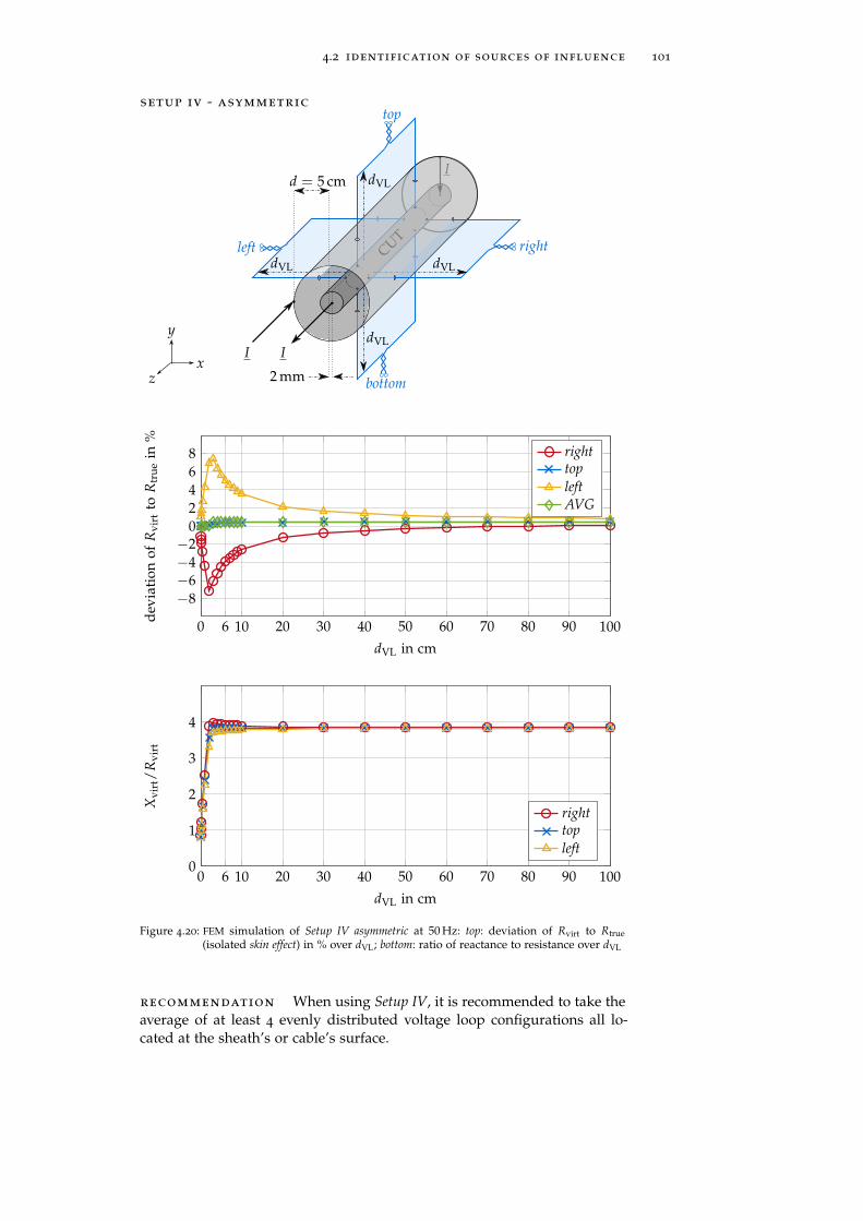
4.2 identification of sources of influence 101
setup iv - asymmetric
x
y
z
I
I
CUT
dVLdVL
dVL
dVLI
rightleft
bottom
top
d = 5 cm
2mm
0 6 10 20 30 40 50 60 70 80 90 100
−8−6−4−202468
dVL in cm
deviationof
Rvirtto
Rtrue
in%
righttopleftAVG
0 6 10 20 30 40 50 60 70 80 90 1000
1
2
3
4
dVL in cm
Xvirt/Rvirt
righttopleft
[ April 27, 2018 at 16:13 – Draft PhD thesis Suchantke ]
Figure 4.20: FEM simulation of Setup IV asymmetric at 50 Hz: top: deviation of Rvirt to Rtrue(isolated skin effect) in % over dVL; bottom: ratio of reactance to resistance over dVL
recommendation When using Setup IV, it is recommended to take theaverage of at least 4 evenly distributed voltage loop configurations all lo-cated at the sheath’s or cable’s surface.

102 recommendations for measurements
setup v - asymmetric
x
y
z
I
I
CUT
dVLdVL
dVL
dVLI
rightleft
bottom
top
d = 5 cm
2mm
0 6 10 20 30 40 50 60 70 80 90 100
−6
−4
−2
0
2
4
6
dVL in cm
deviationof
Rvirtto
Rtrue
in%
righttopleftAVG
0 6 10 20 30 40 50 60 70 80 90 1000
1
2
3
4
dVL in cm
Xvirt/Rvirt
righttopleft
[ April 27, 2018 at 16:08 – Draft PhD thesis Suchantke ]
Figure 4.21: FEM simulation of Setup V asymmetric at 50 Hz: top: deviation of Rvirt to Rtrue (iso-lated skin effect) in % over dVL; bottom: ratio of reactance to resistance over dVL
recommendation When using Setup V, it is recommended to take theaverage of at least 4 evenly distributed voltage loop configurations all lo-cated at the sheath’s or cable’s surface.

4.2 identification of sources of influence 103
conclusion The results obtained by FEM simulations clearly indicate aposition-dependency of the measured resistance and reactance. Even thoughthe influence on true losses was set below 0.1 % in the setups, the influenceon measured losses reached values up to 7 %. For every loop, the measuredresistance—obtained by virtual measurement—converges against the trueresistance within 1 % accuracy for increasing loop size.
As discussed earlier, in case of a 2500 mm2 Milliken conductor the minimumradial voltage loop extension should be equal to the conductor diameter,which is in the range of 50 mm to 70 mm. The average of dVL,min = 6 cm istaken for the following evaluations.
Choosing the top or bottom pick-up loop in Setup I or Setup II results ina deviation of measured to true resistance close to zero. The reactance toresistance ratio is 6.65 at 6 cm.
Choosing the top or bottom pick-up loop in Setup III results in a deviationof measured to true resistance of approximately −0.12 %. The reactance toresistance ratio is 6.27. Even at dVL = 1 m the error amounts to only 0.25 %.
Averaging the results obtained by 4 pick-up loops evenly distributedaround the sheath’s surface in Setup IV results in a deviation of measuredto true resistance of approximately 0.44 % directly above the sheath. Whenextending the voltage leads over the sheath, they capture a negligibleamount of sheath losses as discussed later. The top and bottom lead wireconfigurations converge more rapidly against the deviation of 0.44 %than the pick-up loops located right and left of the CUT. The reactance toresistance ratio lies between 3.76 and 3.92 for the different loops.
Averaging the results obtained by 4 pick-up loops evenly distributedaround the sheath’s surface in Setup V results in a deviation of measured totrue resistance of approximately 0.34 % directly above the sheath. This alsoincludes sheath losses. The reactance to resistance ratio lies between 3.82and 3.90 for the different loops. If possible and dVL = dVL,min still holds,one can avoid capturing sheath losses by locating the voltage lead wiresbeneath the sheath’s surface—on its inner side.
The influence observable at smaller loop sizes can be reduced, whenincreasing the return conductor spacing or decreasing asymmetry, eventhough this is sometimes not feasible in practice. Nevertheless, theseidealized simulations neglect the influence of the current feed line andadditional metal in proximity to the setup. Moreover, perfectly placing thevoltage leads in the symmetry planes or on top, bottom, right or left sideof the CUT is hard in reality. Deviations from symmetry will introduceadditional errors in real setups.
From this investigation alone it seems that Setup I, II and III are the mostconvenient and easiest to build. Nevertheless, all setups have to be checkedfor their susceptibility to deviations from symmetry and also on the influ-ence of nearby conductive parts. This is done exemplarily in the next section.
At this stage it can already be concluded that it is advantageous to knowand use the symmetry of each setup. For the sheath return method multiple

104 recommendations for measurements
voltage lead loops should be used, as the asymmetry is not known in mostcases17. Averaging the results obtained by 4 or more evenly distributed pick-up loops around the conductor’s circumference gives very good results inall setups. Surprisingly—in the sheath return methods—only the out-of-phasemagnetic field components seem to leak out to a significant amount stillinfluencing the measured resistance at larger dVL. The reactance is nearlyunaffected by larger loop sizes. This would make these methods less proneto external asymmetries caused by conductive components.
4.2.2.2 Influence of Nearby Metal Framework on Apparent Losses
For Setup I, II and III the top pick-up loop seemed to present a reasonablechoice. For the sheath return method the average has to be taken. In Figure 4.22the influence of a metallic floor is demonstrated for these voltage loop ar-rangements. From Figure 4.15 it was concluded that a grounded copperplate represents the worst case. Nevertheless, the more realistic case of athickness of t = 1 mm is chosen here. The width of that plate is again 4 mand it is located at d = 1 m beneath the conductor.
0 6 10 20 30 40 50 60 70 80 90 100−2
0
2
4
6
8
dVL in cm
deviationof
Rvirtto
Rtrue
in%
top Setup Itop Setup I Itop Setup I I I (a)AVG Setup IV (a)AVG Setup V (a)
0 6 10 20 30 40 50 60 70 80 90 1000
10
20
30
dVL in cm
Xvirt/Rvirt
top Setup Itop Setup I Itop Setup I I I (a)AVG Setup IV (a)AVG Setup V (a)
[ April 27, 2018 at 16:03 – Draft PhD thesis Suchantke ]
Figure 4.22: FEM simulation of all setups at 50 Hz with a thin copper plate 1 m beneath theCUT; top: deviation of Rvirt to Rtrue (isolated skin effect) in % over dVL; bottom: ratioof reactance to resistance from simulation over dVL
17 Helically winding the voltage lead wires around the circumference at distance dVL,min is likelyanother alternative to easily perform a measurement with the sheath return method and only onepick-up loop. This however was not investigated in theory but included in the measurementsin Chapter 5.

4.2 identification of sources of influence 105
conclusion Setup I and II show the biggest influence of the copperplate upon the measured resistance for larger dVL. The reason is thatsuch large return conductor spacings cause a much wider magnetic fielddistribution in the surrounding, which in turn then interferes strongerwith the conductive ground plate. This can also be seen in the reactance toresistance ratio plots. It is important to point out that the influence on otherpick-up loops in these setups (right and left) is even larger. An asymmetricconductive ground relative to the pick-up loop will therefore have a moresignificant impact on the measured values.
Setup III, IV and V are nearly not affected by the metallic ground plate andshow errors below 0.5 % even for larger spacings. Nevertheless, other asym-metries (metallic shelfs,. . . ) could affect Setup III more than the sheath returnmethods, as they produce nearly no in-phase magnetic field components out-side of the return conductor. As there are too many geometrical and electri-cal parameters involved, this example’s only purpose is to raise awarenessfor the influence caused by other metallic parts, instead of directly assessingand comparing different setups.
4.2.2.3 Influence of Variable Sheath Construction Parameters on Apparent Losses
When extending the pick-up loop over the cable sheath, the magnetic fieldinside the sheath will be included in the pick-up loop. At AC it is complex(see Figure 4.16h and Figure 4.16j) and induces a voltage in the pick-up loop,which causes the measurement of additional losses. Figure 4.23 shows theadditionally measured resistance in asymmetric Setup IV. The red, blue andyellow curves show that exact increase in measured resistance, which appearswhen extending the pick-up loop from beneath to above the sheath’s surface.The results are nearly identical for asymmetric Setup V. In the followinginvestigations, the pick-up loops are located at the same places as in theprevious sections.
It can be seen from Figure 4.23 that the true losses of CUT and sheath aremuch larger than the additionally measured losses. In the worst case—leftpick up loop—at 50 Hz the additionally measured losses due to the sheathonly amount to 0.13 %. The influence on the measured resistance directlyarises from the out-of-phase magnetic fields in the sheath, which in turnare directly linked to its AC losses. As AC losses are small for typicalsheath geometries—because of their tubular geometry and usually smallthickness—the influence on the measured resistance is negligible in mostcases at 50 Hz.
Symmetric Setup IV delivers results in the same magnitude but withouta position-dependency. In the symmetric case the out-of-phase magneticfield components are only present in the sheath (similar to Figure 4.3b).Regarding the sheath, subtracting the DC resistance from the true AC
resistance would directly deliver the curve for the additionally measuredresistance. One can therefore conclude that in the symmetric case: the totalout-of-phase magnetic field solely includes the information about totaladditional AC losses. Interestingly there are slumps at specific frequenciesin the right pick-up loop. They arise from specific parameter combinationsand are not further investigated here.
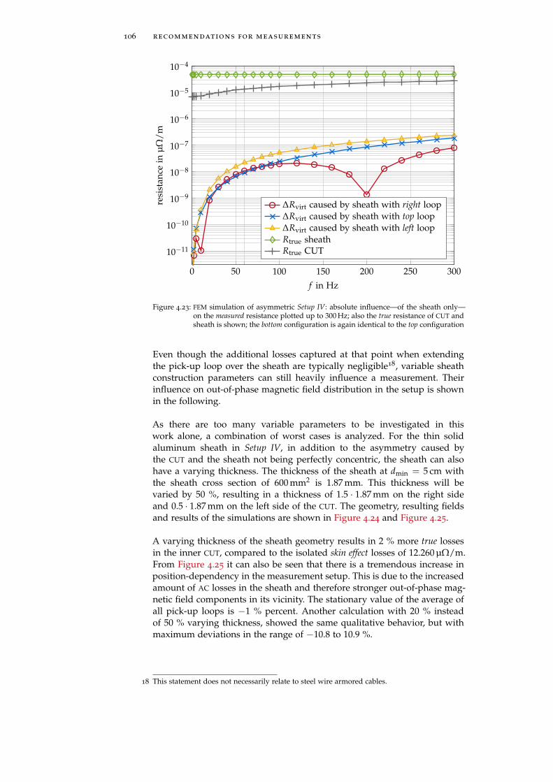
106 recommendations for measurements
0 50 100 150 200 250 300
10−11
10−10
10−9
10−8
10−7
10−6
10−5
10−4
f in Hz
resistan
cein
µΩ/m
∆Rvirt caused by sheath with right loop∆Rvirt caused by sheath with top loop∆Rvirt caused by sheath with left loopRtrue sheathRtrue CUT
[ April 27, 2018 at 15:59 – Draft PhD thesis Suchantke ]
Figure 4.23: FEM simulation of asymmetric Setup IV: absolute influence—of the sheath only—on the measured resistance plotted up to 300 Hz; also the true resistance of CUT andsheath is shown; the bottom configuration is again identical to the top configuration
Even though the additional losses captured at that point when extendingthe pick-up loop over the sheath are typically negligible18, variable sheathconstruction parameters can still heavily influence a measurement. Theirinfluence on out-of-phase magnetic field distribution in the setup is shownin the following.
As there are too many variable parameters to be investigated in thiswork alone, a combination of worst cases is analyzed. For the thin solidaluminum sheath in Setup IV, in addition to the asymmetry caused bythe CUT and the sheath not being perfectly concentric, the sheath can alsohave a varying thickness. The thickness of the sheath at dmin = 5 cm withthe sheath cross section of 600 mm2 is 1.87 mm. This thickness will bevaried by 50 %, resulting in a thickness of 1.5 · 1.87 mm on the right sideand 0.5 · 1.87 mm on the left side of the CUT. The geometry, resulting fieldsand results of the simulations are shown in Figure 4.24 and Figure 4.25.
A varying thickness of the sheath geometry results in 2 % more true lossesin the inner CUT, compared to the isolated skin effect losses of 12.260 µΩ/m.From Figure 4.25 it can also be seen that there is a tremendous increase inposition-dependency in the measurement setup. This is due to the increasedamount of AC losses in the sheath and therefore stronger out-of-phase mag-netic field components in its vicinity. The stationary value of the average ofall pick-up loops is −1 % percent. Another calculation with 20 % insteadof 50 % varying thickness, showed the same qualitative behavior, but withmaximum deviations in the range of −10.8 to 10.9 %.
18 This statement does not necessarily relate to steel wire armored cables.

4.2 identification of sources of influence 107
(a) Setup IV - ||B|| (b) Setup IV - Im(B)
Figure 4.24: Magnitude and out-of-phase magnetic field of asymmetric Setup IV with varyingsheath thickness of 50 %
0 6 10 20 30 40 50 60 70 80 90 100−40
−30
−20
−10
0
10
20
30
40
dVL in cm
deviationof
Rvirtto
Rtrue
in% right
topleftAVG
[ April 27, 2018 at 15:50 – Draft PhD thesis Suchantke ]
Figure 4.25: FEM simulation of Setup IV: influence of varying sheath thickness of 50 % on themeasured resistance at 50 Hz; the deviation to the isolated skin effect resistance of theinner CUT is given for different pick-up loop sizes and locations; bottom is identicalto top
For the copper wire screen the circumferential distribution of the singlewires can be inhomogeneous. This is achieved by shifting every secondwire by 4°, rotating one wire to the center right side and rotating onewire further away from the center left side. Note that the symmetry isbroken and the bottom pick-up loop will no longer deliver identical resultscompared to the top pick-up loop. When considering short measurementlength with the sheath return method, one could also assume an asymmetriccurrent distribution in the sheath wires due to a non-ideal short-circuitat the end of the cable. The geometry, resulting fields and results of thesimulations are shown in Figure 4.26 and Figure 4.27.
The inhomogeneous circumferential distribution of the copper sheath wiresincreases the true AC losses of the inner CUT by only 0.02 % compared tothe isolated skin effect losses of 12.260 µΩ/m. In other words, the inhomoge-neous distribution of sheath wires does not alter the AC losses significantlycompared to the case of homogeneous distribution. In line with this obser-

108 recommendations for measurements
vation, it can be seen from Figure 4.27 that the maximum deviation is in thelower percent range and even lower compared to the homogeneous distri-bution of sheath wires. The stationary value for the average of all pick-uploops is 0.26 %. Again, in this case—if the measuring length is much largeror an integer of the lay length of the wire screen—the position-dependencyof the measurement will likely be reduced, as this equals an averaging.
(a) Setup V - ||B|| (b) Setup V - Im(B)
Figure 4.26: Magnitude and out-of-phase magnetic field of asymmetric Setup V with inhomo-geneously distributed sheath wires
0 6 10 20 30 40 50 60 70 80 90 100−2
−1
0
1
2
3
4
dVL in cm
deviationof
Rvirtto
Rtrue
in% righttopleftbottomAVG
[ April 27, 2018 at 15:44 – Draft PhD thesis Suchantke ]
Figure 4.27: FEM simulation of Setup V: influence of inhomogeneous distribution of sheath cop-per wires on the measured resistance at 50 Hz; the deviation to the isolated skin effectresistance of the inner CUT is given for different pick-up loop sizes and locations
Even though, the examples above present rather extreme cases—at least forthe solid aluminum sheath—one can derive the following conclusions fromthese investigations:
I Variations in the sheath geometries, whether inevitably caused by con-struction or by drumming or further handling the cable, can result inadditional asymmetries in the setup. In turn they can influence themeasurement to a certain degree, which depends on the AC losses inthe sheath and the asymmetry.

4.2 identification of sources of influence 109
I Inhomogeneities in the sheath wire distribution seem to have lessimpact on the measurement, than variations in thickness for solidsheaths.
The results of this chapter also coincide with observations made previouslyin [Suc14]. These stated that additional losses—only measured, when cableswith solid sheaths are drummed—can possibly be attributed to the fact thatasymmetries in the sheath current distribution are much more significantin solid sheaths than in cables with sheath wires. Drumming a cable witha solid sheath does not only give a preferred path for the current to flow,which is at the inner side of the cable drum19, but can also give rise tomechanical induced variations in the solid sheath geometry. These asymme-tries produce much more out-of-phase magnetic fields in the cables vicinityand can cause more proximity effect losses on a drum.
4.2.2.4 Influence of Additional Measurement Setup Factors on Apparent Losses
When setting up a measurement, additional possible influences on the mea-sured resistance can arise from the setup due to practical restrictions. Someof them are discussed in the following. The purpose of these investigationsis to give further insights into possible error sources by presenting somebasic examples.
current transition at voltage tap-off position In Setup IVthe CUT uses a tubular aluminum conductor as the current return. If theCUT is part of a cable and the tubular return is the cable sheath, one hasto cut open a window in the sheath and insulation to reach the surface ofthe CUT with the voltage tap-offs. This gap or window has to be bridged bythe current return path to keep the circuit closed. This bridging is referredto as current transition and displayed in Figure 4.28. Depending on howthe current transition is realized, it can affect the measurement. Of coursethis effect depends on the overall measurement length and becomes morecritical as the measurement length decreases.
The following simulation results account for a total measuring length lmeasof 1 m at 50 Hz. Moreover, d is chosen as 5 cm as previously, dVL as 6 cm andattached in the center of the window. The aluminum sheath cross section isagain 600 mm2 and the setup is symmetric to focus on the effect of currenttransition alone. The current transition is realized by a copper wire with across section of approximately 19.6 mm2 in a transition window of 10 cmlength.
The simulated deviation to the isolated skin effect resistance, which wouldbe measured in case of a perfectly concentric current transition—neglectingthe small additional losses caused by the sheath—amount to:
I 13.2 % for top,
I −5.7 % for right (which is identical to left due to symmetry),
I 4.6 % for bottom,
I 1.6 % for the AVG of all pick-up loops.
19 This is due to the fact that the side of the sheath facing the drum center presents a shorter andhence less resistive path for the current.

110 recommendations for measurements
10 cm
sheath
currenttransition top
x
yz
right
bottom
left
(a) Simulation setup; note that the pick-uploops location (in the coordinate system)is consistent to the setups analyzed previ-ously
y
zx(b) Out-of-phase magnetic fields at voltage
tap-off position; the viewer looks in direc-tion of the z-axis, which is also the direc-tion of the current in the CUT
y
zx
(c) Cut view of resulting outer out-of-phase magnetic fields at different positions along theconductor axis and ||J|| in CUT and sheath (scaled differently); this picture shows both:skin effect only (at the left and right end of the CUT) and proximity effect at the positionof current transition
Figure 4.28: The current transition remains in the same top position; again the 4 pick-up loops(right, top, left, bottom) around the circumference are deployed and attached to theCUT’s surface
Figure 4.28c and additional evaluations also show that the influence ofthe out-of-phase magnetic fields upon the loops rapidly decreases behindthe current transition. Also, it is interesting to note that its influence afterthe current transition acts in a way that decreases the effect of the currenttransition. In other words, the outer out-of-phase magnetic fields have anopposite direction after the current transition than at the place of the currenttransition.
Recollect that a perfectly concentric current transition would have no influ-ence. In that case only the out-of-phase magnetic fields in the sheath wouldaffect the measured resistance as discussed in the previous section. In theinvestigated setup the outer out-of-phase magnetic fields affecting the mea-sured resistance, again arise from the rotational asymmetry in the currentdistribution—due to the current transition—in and close to the window. Toavoid these effects one should try to achieve a current transition as concentricas possible. This can—for example—be achieved by using two half shellsto form another tubular conductor enclosing the gap (see Figure D.3b).Nevertheless, even then one would need to drill holes in the sheath to reachthe CUT with the voltage lead wires, which affect the current distribution init and may influence the measurement. This is shown in the next paragraph.
It has been found that the current transition can heavily influence the resultsand should be considered or avoided in a measurement setup. The influenceon measured resistance will decrease with increasing measuring length lmeas.

4.2 identification of sources of influence 111
drill holes in a tubular return conductor Again symmetricSetup IV is considered as guiding the voltage leads through a wire screenor any other non-solid sheath does not present a challenge. Drilling holesis only practical, if the there is no insulation between CUT and tubular re-turn conductor. Figure 4.29 shows the influence of a small drill hole with adiameter of 5 mm on the current density in the sheath.
Figure 4.29: Cut view of Setup IV with a drilled hole in the sheath; ||J|| in CUT and sheath(scaled differently) and current streamlines in the sheath are shown
As concluded by the previous section, the influence depends on the ratioof asymmetry (drill hole dimension) to measurement length lmeas. As thisratio is typically very small, no significant influence is expected upon theresults by drilling small holes in the sheath. Moreover, the investigation ofasymmetric sheath wire distribution indicated only negligible influences ofsmall irregularities in the sheath geometry.
short-circuit at the end of sample When making a connectionfrom CUT to return conductor, one introduces additional magnetic fieldcomponents. These are in-phase and eventually out-of-phase components.Taking Setup I as an example, in 2D one would not have magnetic fieldcomponents in direction of the axis of CUT or return conductor. A short-circuit at the end connecting both would introduce these components.Depending on distance and position of the pick-up loop it can affect themeasurement. This is no problem for the previously favored top or bottompick-up loops in Setup I, II and III as their surface normal is perpendicularto all magnetic field components introduced by the short-circuit. Eventhough one should keep this effect in mind when analyzing a setup, theinfluence of the short-circuit can easily be diminished. As the magnitudeof the magnetic fields is proportional to the reciprocal of the distance fromthe short-circuits surface, setting the distance from the pick-up loop to theshort-circuit much larger than dVL will rapidly decrease the influence. Thiscondition is easy to achieve in every setup and laboratory and is thereforenot further investigated here.
A similar, much more relevant question on how far the current injection hasto be placed apart from the voltage tap-offs is addressed in Section 4.2.3.
4.2.2.5 Further Notes on Influences on Apparent Losses Due to the Pick-Up LoopLocation
Another important fact open for investigation is the influence of deviationsfrom symmetry, which could have a large impact on the measured value.Moreover, as pointed out previously, when benchmarking a measurementsetup with a known reference conductor, one should consider influences

112 recommendations for measurements
by the subsequently measured CUT. What needs to be avoided is directlyapplying the setup used for the reference conductor to the CUT without fur-ther considerations (e.g.: how does dVL,min change, how does the magneticfield of the CUT influence the surrounding compared to the fields of thereference conductor,. . . ).
Moreover, some other variational geometric parameters of the cable or theCUT could be checked for their influence, more specifically the ovality of theCUT or complete cable. Some exaggerated impressions of manufacturing-depend fluctuations in cable geometry are shown in Figure 4.30.
(a) Displaced segments (b) Oval inner conductor (c) Oval cross section
Figure 4.30: Exaggerated illustration of possible cable geometry fluctuations due to the manu-facturing process of the cable; courtesy of Südkabel GmbH
4.2.3 Influence of Current Contact System and Resulting Current Homogeniza-tion
The current distribution in combination with its resistivity determines thetrue losses of a conductor. They are lowest when the current density in across section is completely homogeneous [Gra79, p. 32]. The current injec-tion into a conductor can enforce current distributions and therefore influ-ence its true losses. This is called end effect or terminal effect. In an electricalmeasurement its influence on the measured resistance depends on:
I the type of contact/contact system (e.g.: how much of the cross sectionis connected to the current injection, how good is the connection,. . . ),
I geometrical and electrical parameters of the CUT and measurementsetup (e.g.: conductivity, applied frequency, strand insulation,. . . )
I distance from current injection to the voltage tap-offs of the pick-uploop.
In the measurement it is desired that the current density in the measuredsection is identical—representatively—to the current density in most partsof the conductor under operation20. In a long cable a steady currentdistribution in the cross section is expected along the majority of the overalllength. Thus, the current density in the measured section should not beinfluenced by any end effects either, to give results of practical relevance.Moreover, it is desired that the practical expense to set up the connectionsat both ends of the cable is as low as possible. This expenditure also
20 Note that this only refers to the distribution and not the magnitude of the current densityas only linear conductors are considered, where the AC resistance does not depend on themagnitude of the current.

4.2 identification of sources of influence 113
depends on the magnitude of the test current—which is small with themeasurement system used in this work—but can be much larger using otherequipment and hence result in specially designed connectors as in [MBD15].
In the following, some references including theoretical considerations andmeasurements regarding stranded conductors are given. It is followed bya short FEM investigation of a small stranded conductor including differenttypes of current injections. At the end, based on these preceding investiga-tions, practical measures are discussed.
4.2.3.1 Past Work and Theoretical Considerations
A very early remark on the current homogenization in conductors is madeby J. C. Maxwell, when considering the measurement of small resistances:
“At a short distance from the extremities the current becomes sensiblyuniform.” [Max73a, p. 405].
It is clear that this general statement depends on multiple factors as notedabove, especially on the quality of the electrical contact connecting thecurrent path (also called current leads) to the CUT. Extensive studies onelectrical contacts in general can—for example—be found in the “ElectricContacts Handbook” [Hol58] and in [Vin16]. These analyze the influenceof temperature, mechanical stress and different contact types such assliding, switching and stationary contacts, whereas only the latter is ofrelevance in this work. Analytical solutions for the current homogenizationin conductors can be found in [HM76; BM86; MS13, p. 112; ZL13]. Morerecent and advanced works on long-term behavior of different contactsystems are found in [Gat+14b; Gat+16] for example.
One study, which focused on the current homogenization in stranded con-ductors at DC is [Bür95] by Jens Bürkner. The goal here was to accuratelymeasure the contact resistance between a connector and a stranded conduc-tor. In this case it is also necessary that the measurement is not influencedby inhomogeneous current distributions caused by the electrical contact be-tween the connector and the following stranded conductor. This problem isschematically displayed in Figure 4.31.
AL
stranded conductor
...
x
y
z
contact
I
?
b
...
connector
a
...
Figure 4.31: Current homogenization at DC after a punctiform contact based on [Bür95, Bild2.1]; a marks the first voltage tap-off; the necessary distance to second voltagetap-off b on the stranded conductor was investigated in [Bür95]
For the DC measurement the author concluded that there are 3 possiblecountermeasures against inhomogeneous current distributions, caused bythis contact:

114 recommendations for measurements
1. One can take the measurement at a position, far enough apart from thecontact, where the current density is homogeneous in the cross section.In stranded conductors, this distance depends on the contact resistancebetween the single strands in the bundle. This distance approacheszero if the strands have a contact resistance, which is much lower thanthe resistance along the strand (extreme case is a solid conductor) andapproaches infinity, if the contact resistance is much larger than theresistance of the strand. For example: in case of an ACSR the minimumnecessary distance ranged from 0.9 m to 9 m. For an aluminum single-core cable this distance was much lower with 0.9 m to 1.8 m, due tothe mechanical forces by the insulation, which decreased the contactresistance between strands [Bür95, p. 13].
2. Another option is to equalize the current density in a cross section byshort-circuiting all wires. Setting up a low resistance contact betweenall wires forces the current density to homogenize faster. For a small7-strand cable this was achieved by connecting an additional low re-sistive wire ring around the periphery of the bundle [Bür95, p. 16].
3. The last option is to perform a measurement on every single strand inthe cross section and then calculating the average value [Bür95, p. 20].This is not feasible for M-type conductors, which can easily containmore than 500 strands.
From these results it follows that one needs to have a current injection ashomogeneously as possible or may give the current a certain distance to ho-mogenize in the cross section. Therefore, some FEM examples are displayedin the following to get an impression on how current homogenization canoccur in stranded conductors with insulated strands. As argued previously,due to small test currents of only a few A, no rise in conductor temperatureis expected, if the CUT is a power cable. Thus, the effect of temperature isneglected in the following simulations21.
Concerning the voltage tap-offs, a deeper discussion on how to optimallyconnect them at AC and DC is given in Section 4.2.4.
4.2.3.2 FEM Simulations
Concerning solid and tubular conductors, previous FEM simulationsin [SPS16] showed that current homogenization along the conductor axisappears rapidly. In a solid circular 2500 mm2 copper CUT, independentof the position of punctiform current injection into the cross section, thecurrent density around the conductor’s circumference deviates no morethan 0.4 % compared to that of a homogeneous injection after 15 cm, whichis slightly below 3 times the conductor diameter. This recommendationof necessary length for current homogenization being at least 3 · dCUT, isused again later in this work. Generally, the necessary length for currenthomogenization becomes shorter with increasing frequency and conduc-tivity. Another more general statement for solid conductors at DC is givenby [Bür95, p. 6] and states that at a distance of approximately 0.75 times thewidth of the conductor, the current density is nearly identical in the wholecross section.
21 Nevertheless, of course small temperature gradients could arise at constriction resistances atthe contact points.

4.2 identification of sources of influence 115
In the following investigation, these studies are extended to the case ofa stranded copper CUT composed of 19 (1 + 6 + 12) perfectly insulatedstrands, again with a total cross section of 2500 mm2 and a rms test currentof I = 1 A. Every wire has a perfect insulation of 100 µm thickness. The firstlayer has a lay length of 25 cm and the second, outer layer has a lay lengthof 50 cm. Again, the excitation is realized by a current source at a frequencyof 50 Hz. Generally, in addition to possible contact resistances betweenstrands, at AC the current distribution is also affected by proximity effect.For DC, behind the current injection22 the current density is only furtheraffected by the contact resistances between strands.
Figure 4.32 shows 3 different setups and the current densities at AC in thecenter plane of the model. In the first setup, a homogenized current injec-tion is realized by a solid copper plate at both ends of the CUT. The lossesproduced by this current distribution serve as the desired reference losses.Here, the losses at 50 Hz are calculated to 12.56 µW/m.23 The second setuprealizes the current insertion with a ring, connecting all strands of the outerlayer exclusively. The third simulation model shows an extreme case, whereonly the central wire is connected to the current path of the measurementcircuit at both ends. The overall length of every model is 42 cm and thelosses are evaluated in a 1 cm long section at the center of the model.
(a) Homogeneous current injection (desiredreference)
(b) ||J|| 21 cm behind current injection in caseof homogeneous contact
(c) Current injection via ring in the outer layeronly
(d) ||J|| 21 cm behind current injection in caseof a ring contact
(e) Current insertion into central wire only(worst-case scenario)
(f) ||J|| 21 cm behind the current injection inthe central wire only
Figure 4.32: The blue areas indicate the terminal, where the current is injected; the maximumcurrent densities in all figures are normalized to the maximum value of Fig-ure 4.32b; note that therefore in Figure 4.32f the current density in the central wireis off the chart, as it is approximately 10 times larger than the maximum currentdensity in the other plots; the terminal at the opposite side (not shown) is identical
22 Current injection refers to the connections of the current path to the CUT on both sides of theconductor. Observations and conclusion drawn are therefore also valid for both sides if notnoted otherwise. Current injection is therefore equal to the current extraction on the oppositeside.
23 This is slightly larger than the losses by a solid CUT with 12.26 µW/m as stranding can increasethe absolute resistance due to longer current paths.

116 recommendations for measurements
The homogeneous current injection in Figure 4.32b shows the desiredcurrent density in the bundle24. Figure 4.32d shows a larger deviationfrom homogeneity in the cross section compared to the homogeneous case.Currents in the outer layer will set up eddy currents in the inner layer andcentral wire. These eddy currents are not part of the test current and onlycause additional losses. They flow in one direction at one part of a strandand in the opposite direction on the other side of a strand. The injectedcurrent has to flow over the outer layer only, which in turn increases theoverall losses to about 13.39 µW/m. Similar thereto, Figure 4.32f showsthe current density at AC, if the current is only injected into the centralwire. Eddy currents are excited in the 2 adjacent layers. Forcing this constantcurrent through only 1/19 of the cross section (central wire only) results inlosses of 147.64 µW/m.
These results make the problem with insulated wires clearer: on one hand,it is desired to have a perfect insulation of the single wires to reduce AC
losses in the Milliken design. On the other hand, this would require thecompletely homogeneous injection of the test current in the cross section tohave a representative current distribution (Figure 4.32b) in a measurement.
In practice, depending on the manufacturing quality and effort put into theinsulation of the single strands, it is likely that some low resistive contactsbetween strands are present. The number and quality of these interwirecontacts clearly depend on multiple parameters from exact conductor de-sign to manufacturing processes and can be affected by further handling ofthe cable also (drumming, heating, . . . ). Table 4.3 includes some examples,where contacts between strands have been included in the 19 wire strandedconductor with a current injection into the central wire only. Note that theboundary condition at the opposite side affects the current homogenizationin the simulation as well. For the contacts to show any significant effect, itwas assumed here that the complete cross section is grounded at the sideopposite from injection.
Table 4.3 shows the following: concerning the homogeneous current injec-tion (I.) it can be seen that the DC resistance is larger compared to a solidcopper CUT with the same overall cross section (RDC,Ref = 6.897 µΩ/m). Thereason is that the path the current has to follow is longer in the layers dueto the helical winding. Nevertheless, the resistance ratio of 1.64 is smallerthan that of a solid conductor with 1.77 at 50 Hz. For the injection via a ringinto the outer layer (II.), the resistance ratio is smallest because the currentdistribution at DC is already similar (mostly in the outer layer) to the currentdensity enforced by skin effect at AC. An injection into the central wire only(III.) results in the largest absolute losses. At DC they are approximately 19times larger compared to the homogeneous case because only 1/19 ofthe cross section is used. Setting up small conductive contacts betweencentral wire and all 6 wires of the inner layer and 6 “contacts” between thestrands of this first layer and the 6 strands of the outer layer (IV.), whichdirectly face the 6 strands of the first layer, reduces losses significantly. Notethat losses are still larger because in the remaining strands of the outerlayer, which have no direct contact with the current path, eddy currents are
24 In theory, losses could be lowered by balancing the injected current in the layers with theimpedance caused by their AC and DC resistance, to have a completely uniform current densityin the cross section. This however does not relate to any case of practical relevance.

4.2 identification of sources of influence 117
excited. Two “contacts” (V.) are much better because in this special case allstrands of the second layer are connected to the current path and thereforeparticipate in transporting the test current, hence reducing losses.
Homogenization appears nearly instantly behind highly conductive contactpoints. Then the distance to the voltage tap-offs would nearly play no role.If the conductivity of the contact is lower than that of the conductor mate-rial, the necessary distance for current homogenization directly depends onthe ratio of longitudinal strand resistance to contact resistance. Then, longersamples might be necessary as the resistance of the contact remains con-stant, while the longitudinal resistance increases with conductor length. Anincreased distances between injection and voltage tap-off can also help as itis likely that more contact points are present between the strands. This in-creases current flow over the contact points, which in turn improves currenthomogenization. The influence of this resistance ratio was analyzed for DC
in more detail in [Bür95].
Table 4.3: Comparison of different configurations in the 42 cm long 19 strand bundle; “contacts”relate to a contact surface of 1 mm× 0.5 mm between central wire and all strands ofthe first layer and 6 equal transitions between first and second layer, where strandsdirectly face each other
configuration losses at DC losses at AC losses
in µW/m in µW/m AC/DC
I. homogeneous current injection, 7.65 12.56 1.64
all wires perfectly insulated (reference)
(Figure 4.32a)
II. current injection in layer 2 only, 12.17 13.39 1.10
all wires perfectly insulated
(Figure 4.32c)
III. current injection into central wire only, 131.82 147.64 1.12
all wires perfectly insulated
(Figure 4.32e)
IV. current injection into central wire only, 24.08 43.53 1.81
“contacts” 4.25 cm after injection
with a conductivity of 1 · σCu
V. current injection into central wire only, 8.46 12.94 1.53
2 “contacts”: 4.25 cm & 8.5 cm after
injection with a conductivity of 1 · σCu
VI.current injection into central wire only, 41.20 46.29 1.12
2 “contacts”: 4.25 cm & 8.5 cm after
injection with a conductivity of 1 MS/m
(this is equal to the resistance caused by a
strongly oxidized copper surface [BM11])

118 recommendations for measurements
4.2.3.3 Practical Considerations
Due to practical limitations, one wants to keep the necessary length fromcurrent injection to voltage tap-off as short as possible. Thus, current ho-mogenization has to be established as fast as possible along the conductoraxis. Therefore, in a conductor with insulated wires one needs to establisha contact over the whole cross section at both ends of the specimen. Toachieve that, one could use copper braids, low-melting solders or someother kind of conductive contact gel at both terminals, which reachesevery wire in the cross section. Special designs with many needles pushingagainst the cross section reaching every single strand would be a properway to achieve a homogeneous current injection.
Figure 4.33 shows the contact system used by TU Berlin in the measure-ments of Milliken conductors. It uses a simple copper weave to reach asmany of the insulated strands as possible. Even thought not all strands willbe reached, the procedure described in the next section shows why it works,if the conductor is further processed.
Figure 4.33: Simple current contact system used by TU Berlin for Milliken conductors; a copperbraid is used on the inside to increase the contact area
Even though the exact way of current injection was not described, in [Sjö13],where the CUT was a 2000 mm2 Milliken conductor with bare wires and 20 mlength, it was observed that the influence of the end effect is already be-low 0.5 % at a distance of 20 cm from the current injection and not presentat all after 60 cm. As no further information about the contact system atthe terminals was given, this example only gives some ideas about currenthomogenization.
4.2.3.4 Conclusion
Current homogenization along a stranded conductor with insulated wiresis either achieved by establishing a good contact to every single strand atboth ends, or by having good electrical contacts between strands, whichboost current homogenization along the conductor axis. Moreover, behindgood electrical contacts and in solid conductors, current homogenizationappears rapidly.
From the FEM simulations some conclusions regarding current homog-enizations could be drawn. A lot is still open for investigation: e.g.homogenization in M-type designs, different contact resistances betweenstrands and so forth. An important general statement concerning the

4.2 identification of sources of influence 119
current injection, which can be derived from references and precedinginvestigations is that the current injection should be as homogeneously aspossible, as one cannot rely on good electrical contacts between strands inM-type conductors with oxidized or enameled wires.
The important influence of voltage tap-off positioning is described in thenext section.
4.2.4 Placement of the Voltage Tap-Offs Including Conductor Preparation
This section also serves as a conclusion of some observations and statementsmade previously in different sections. The placement of the voltage tap-offsis strictly linked to the question of current homogenization.
There are certain requirements about the positioning of the voltage tap-offson Milliken conductors or conductors with insulated wires in general.
I At DC: To accurately measure the DC resistance between two points aand b in a complex conductor composed of multiple insulated parallelstrands, one has to meet the following two requirements:
1. The current distribution in this section has to be representativefor the operating condition. This means that every strand in thissections between a and b has to take a part of the test current.The more parallel strands are available for the test current thefewer DC losses appear. This can be achieved by establishing atleast one good electrical contact between all strands before volt-age tap-off a and after voltage tap-off b or a completely homoge-neously current injection. If a perfect injection cannot be guaran-teed, the safest way to establish a good electrical contact betweenall strands is welding the conductor at both terminals. This en-ables quick current homogenization after the injection in this—now solid—conductor section. Alternatively, the insulation on thestrands can be removed at both terminals followed by mechan-ically compressing all strands to enable good contact betweenthem. Another alternative, which relies on interwire conductiv-ity, is to give the current sufficient length along the conductor tohomogenize in the cross section. The distance between voltagetap-offs and current injection then has to be increased. This ofcourse does not guarantee that all strands have contact to the cur-rent path and can lead to the measurement of an increased DC
resistance.
2. One needs to assure that both voltage tap-offs, a and b, are at-tached to the same strand. If this is not the case, contact re-sistances between wires are included in the measurement. Thisis also achieved best when attaching the voltage tap-offs to theblank, solid section described by 1. (for example by welding). Ifnot welded, it can be hard and lavishly to retrieve the same strandat the rear voltage tap-off b. Moreover, this strand is not necessar-ily located at the surface in M-type designs due to the twist oflayers.
I At AC: The same requirements as for DC are necessary. As at DC, theo-retically, it would be sufficient to contact the voltage tap-offs to one

120 recommendations for measurements
individual strand only at both voltage tap-offs—assuming a repre-sentative current density is already established in the cross section—because the outer out-of-phase magnetic field components capturedby the pick-up loop contain the information about AC losses of thecomplete conductor bundle (also see Appendix A.2)25. Again, fromthe practical side of view it is much safer to electrically connect allstrands at the voltage tap-off positions by welding for example.
For both excitations, AC and DC, it is important that between the tap-offs aand b the conductor has to have the design it was intended to have: e.g.insulated wires for AC loss reduction. This guarantees that the increase ofDC resistance, due to longer helically current paths in the single insulatedwires, is measured correctly as it will occur under operation as well. At AC
it will guarantee that the loss optimized Milliken design is measured. Onepossible and recommended way to connect the voltage tap-offs is shownin Figure 4.34.
I
...segment 1 segment 2
M-type conductor
insulated strands
blank section(solid, if welded)
...umeas
...
AL
x
y
z
welded terminal
a
symmetry axislmeas/2
lto,i
Figure 4.34: One possible way to position the voltage tap-offs at a and b on a Milliken conductorwith insulated strands; only one end of the conductor is shown, voltage tap-offb is located on the far right side and connected identical to a; the gray shadeindicates blank strands/conductor parts and the red area symbolizes insulatedstrands/conductor parts
Concerning the distance between voltage tap-off on the blank section andbeginning of the insulated section—length lto,i—one has to regard the fol-lowing at DC and AC:
I On one hand, the connection between all strands should still be verygood, so that the electric scalar potential is still constant in the crosssection.
I On the other hand, lto,i lmeas should hold, so that the representativeconductor section (red shaded area in Figure 4.34) is mainly influenc-ing the results. Due to removing the insulation of the strands at theterminals and voltage tap-off positions, at DC the local losses near thevoltage tap-offs are smaller compared to the insulated section, becausethe current does not have to follow longer helical paths. At AC the local
25 As discussed earlier, this of course is only valid when dVL ≥ dVL,min.

4.2 identification of sources of influence 121
losses near the voltage tap-offs are larger, because this blank conduc-tor section is not optimized and has therefore full AC losses comparedto the optimized Milliken conductor design in the middle section.
This is schematically depicted in Figure 4.35. It shows simulation results atDC including the electric scalar potential and current density.
I
blank section(solid, if welded)
...umeas
AL
y
x
welded terminal
a
symmetry axis
lmeas/2
lto,i
insulated strands(different DC resistances)
...
Figure 4.35: 2D DC FEM simulation of inhomogeneous current injection into the blank terminalof a conductor with perfectly insulated strands, which have different conductivi-ties; recommended position of voltage tap-offs a and b (b is not shown, but identi-cal to a) is indicated; current streamlines are color-coded according to the absolutecurrent density and the equipotential lines are shown in black
It was made clear that a Milliken conductor has to be further processed forthe succeeding measurement. All strands should have electrical contact ifperfect current injection cannot be guaranteed. This is also valid for blankMilliken conductor designs as oxides can form on the strands and the seg-ments are usually separated by thin tapes. In practice this can be achievedby one of the following ways:
I Welding the terminals of the cable, using thermite for example, toform a solid conductor as shown in Figure 4.34 and Figure 4.35 islikely the most reliable way to guarantee that all strands are electricallyconnected.
I Alternatively, one can remove the insulation of all single strands andmechanically compress the bundle to further decrease contact resis-tance between strands. This can be done by a conductive ring clampor high current connector. The clamp should be conductive to equal-ize the electric scalar potential over all segments, which are typicallyinsulated from one another by thin tape. Of course the tape can alsobe removed in the first place. Yet the clamp should not contain anyferromagnetic materials as this could locally increase losses at AC. In

122 recommendations for measurements
case of enameled wires the insulation can be scraped off with a knife,be removed chemically or be removed with a sandblaster for example.In the case of oxidized strands, it can be sufficient to apply strong me-chanical pressure to the individual wires, as the thin oxide layers onthe strands then break open. Oxides on copper conductors can easilybe removed by using a citric acid solution.
Both approaches of conductor preparation are relatively time-consuming.But it is recommended that the conditions put forward above are met, be-cause one will likely still obtain a measurement result, if these preparationsare not made, but a result, which likely includes contact resistances. Thesame conclusion was drawn by [BM11], where the authors developed a sys-tem to accurately determine the DC resistance of small insulated conductorbundles. From the practical side of view, independent of the chosen method,one should check the DC resistance with expectations. If the DC resistanceis in agreement with the expectation, the chosen approach is adequate, asDC losses directly indicate the number of strands participating in currenttransport. If DC losses meet the expectation, the whole cross section is usedand possible contact resistances included in the measurement are negligible.Even in enameled Milliken conductor designs it was observed that injectingthe current in only one of the hundreds of strands in the cross section,shows good compliance with the calculated DC resistance if the voltagetap-offs are placed sufficiently far away (0.5 m to 2 m) from the injection,even though placed on the blank surface of an enameled section.
From this section it becomes clear that if all the above conditions for thevoltage tap-offs are met, the current injection is not a critical part anymore.The reason is that current homogenization appears rapidly in solid, ratheruninsulated conductors, which should be present at both terminals.
4.2.5 Additional Sources of Influence Open for Investigation
This section shortly lists additional possible sources of influence upon themeasurement, which were not further investigated in this thesis. Thesepoints are discussed again later in Chapter 6.
minimum measurement length The AC resistance of a Millikenconductor is influenced by its 3D geometry, due to the twisting of thesegments and layers. This is opposite to a solid cylindrical conductor forexample, where every cross section along the conductor axis is identicaland therefore making it a 2D problem.
The question should be raised at which length a sample used for a mea-surement shows the same behavior as the complete cable. When using asample of only a couple of meters in length, the mutual induction betweendifferent insulated layers—which directly affects the current density in thelayers—can be different compared to a much longer sample. An examplefor clarification: having a twisted pair cable with some space betweenboth wires and both ends short-circuited, placed in an external alternatingmagnetic field, will induce a current in the single wires depending on thenumber of twists (also see [Ros18, Figure 2.4]). If the number of twistsis an integer, the total induced current will be zero, because inducedcurrents will cancel each other out. If the number of twists is not an integer,eddy currents will flow in the twisted pair cable and therefore change its

4.2 identification of sources of influence 123
losses. Nevertheless, induced currents will successively decrease with anincreasing number of twists. In a complex conductor, such as the Millikenconductor, the exact position of each strand towards each other strand, willlikely not repeat (be the same again) in short samples. This lowest commonmultiple of the lay lengths of layers and segments—where the complete 3Dgeometry starts to repeat—will probably be larger than the measurementlength as shown in the following example: [Joa98, p. 45] gives the laylengths of a 2500 mm2 Milliken conductor, where the segments and 2 of 3layers are stranded. With the segment lay length of 2.15 m, a lay lengthof 0.29 m for the second and 0.33 m for the third layer, the lowest commonmultiple amounts to roughly 2000 m.26 Theoretically, only after this distanceall wires in a layer have been exposed to the same electromagnetic fielddistribution—caused by the other segments—and therefore have the samecurrent density and AC losses. Despite this length being already larger thantypical production lengths, having a sample of only a couple of metersin length will probably not show the exact same behavior compared to alonger cable.
The necessary minimum measurement length pertains all measurementmethods equally, including the calorimetric approach. In the measurementsperformed in this thesis a measurement length of at least 5 m was tried tobe realized. For typical designs this includes multiple segment lay lengths.
influence of drumming of the cable Already in [Gra79, p. 98] ithas been noted that the insulation of the single strands can be damagedby mechanical force upon the segments during manufacturing, reeling andunreeling. Damage caused by the manufacturing process will be visible inthe measurement. Nevertheless, it is unknown if and how the performanceof a cable with insulated strands is affected after the cable has been put ona drum and is again reeled off on site.
long-term behavior Load cycles under operating condition of the ca-ble can heat up the conductor of a power cable up to more than 90 C. Heatcan have a direct effect upon the surface of blank copper wires and on theelectrical properties of insulation of the single strands as well. Moreover,heat-ups and cool-downs can have an indirect effect by inducing mechani-cal stress upon the segments and strands in a conductor. This in turn caninfluence the insulation properties of the strands by friction between dif-ferent layers for example. Both effects should be studied. Due to these un-certainties it is questionable if the measurement value obtained at 20 C forexample can directly be corrected to higher temperatures.
26 Another example of a 2000 mm2 Milliken conductor given in [Joa99] has a lowest commonmultiple of approximately 200 m.

124 recommendations for measurements
4.3 recommendations for ac loss measurements with theelectrical method : setup, conductor preparation andprocedure
This section provides a quick overview and uses all results obtained previ-ously to recommend a setup and procedure with only little further explana-tion as this was already done for nearly all points previously.
4.3.1 Conductor Preparation
It is recommended to prepare the Milliken conductor in the following way:
1. In oxidized or enameled designs, the insulation of all strands at bothterminals should be removed by welding or scraping it off for a lengthof ≥ 3 · dCUT. Alternatively chemical methods can be used as well.Then enable a good electrical connection between all strands and seg-ments, for example by applying mechanical pressure.
2. Remove oxide layers (by using sandpaper for example):I from the cross section at both terminals to improve current injec-
tion into the CUT’s cross section,I from the CUT’s surface at the voltage tap-off positions (if it is not
placed at the blank section at the terminals)I and also from the ends of the voltage lead wires them-
selves [HB81, p. 115]27.
3. Establish a conductive circumferential connection at the voltage tap-offs.
4. Connect the current path to the blank terminals as homogeneously aspossible.
Next, the pick-up loops and return conductors have to be set up.
4.3.2 Setup of Pick-Up Loops and Return Conductors
In general one should avoid additional conductive parts, in which eddycurrents can build up, as much as possible.
If it is certain that no additional conductors are nearby (including the labo-ratory floor, shelves,. . . ) then using the symmetrical return method with onepick-up loop will deliver very accurate results. The top configuration is veryrobust against asymmetries from the return conductors. The recommendedsetup in this case is shown in Figure 4.36. The return conductor spacingshould be larger than dmin, which is the case with d = 0.5 m or larger.
In Figure 4.36 the sheath was removed, even though it was shown earlierthat it will not influence the measurement significantly in typical sheathdesigns28. The insulated section of the Milliken conductor (middle sectionin red) has to be kept under the insulation, as the mechanical pressure ofthe insulation can influence the conductor performance. The distance from
27 Further information on films on electric contacts can be found in [Hol58, p. 27] for example.28 Note that cables with special sheath designs or steel wire armored cables can be a special case
and influence the measurement noticeable. This has to be checked in advance.

4.3 recommendations for ac loss measurements 125
voltage tap-offs to the insulated part of the CUT should be much smallerthan the overall measurement length. Current homogenization in the blankconductor sections at the terminals is sufficient after approximately threetimes the conductor diameter. In practice, current homogenization was of-ten observed below this distance. This can also be checked back with FEM
simulations in advance. To avoid the excitation of eddy currents in the sur-rounding as much as possible, the current feed line should be performedcoaxially. This suppresses outer magnetic fields caused by this current path.
x
y
z
I
return
dVL = dCUTreturn
umeas
lmeas>5m
blank/welded
dCUT ≥ 3 · dCUT
(both ends)
I/2 I/2
CUT
I
coaxialcable
0.5m 0.5m
Figure 4.36: Recommended measurement setup for short Milliken conductor samples, if noother conductive parts are nearby; the still insulated section of the Milliken con-ductor is shaded in red; both ends of the CUT are prepared equally
When having additional conductive materials in the surrounding (includingthe laboratory floor, shelves,. . . ) or if it is not known for sure, the averagevalue (AVG) of at least 4 pick-up loops evenly distributed around the cablescircumference at the same dVL should be used. The generally recommendedsetup for an AC resistance measurement is shown in Figure 4.37.
x
y
z
return
return CU
T
II
> 1m
right
top
le f t
bottom
conductive ground
Figure 4.37: Generally recommended measurement setup for short Milliken conductor samples;the still insulated section of the Milliken conductor is shaded in red; both ends ofthe CUT are prepared equally; this setup is also robust with regard to asymmetriesfrom the surrounding

126 recommendations for measurements
The preceding investigations showed that averaging also reduces the nec-essary dVL,min. Hence, the pick-up loops can be attached at the surface ofthe cable. This will also reduce the phase angle of the measurement as well,which is advantageous29. Except for dVL all other parameters are identicalto those shown in Figure 4.36. For the sake of clarity they are not shownhere again. One additional geometrical distance is defined, which is thespacing of the whole setup to a possible conductive ground or wall being atleast 1 m. The reason for that is that the distance to the asymmetry shouldbe as large as possible—even though the AVG is taken—and a distanceof 1 m is easy to realize in practice. Moreover, as discussed earlier, if theDC resistance still meets expectations, one can reduce the distance betweencurrent injection and voltage tap-off or set up a more simple currentinjection and put the voltage tap-offs further away. The DC resistance showsif current homogenization in the cross section is already sufficient.
In general one should avoid conductive parts near the measurement circuitas far as possible. Moreover, if the Milliken conductor is exchanged againstanother CUT one should consider to adapt dVL. Some additional remarks areput forward below:
I The voltage leads should be much thinner than the CUT to avoid aninfluence on the current distribution in the CUT. This can also be easilychecked with FEM simulations in advance.
I Even though the terminals are welded, the current injection should beperformed as homogeneously as possible.
I From the point the voltage lead wires first meet, they have to betwisted together very tightly to avoid further influence of alternatingmagnetic fields. Instead of connecting the voltage leads at the centerof the CUT at lmeas/2, the rear voltage lead wire can also be led alongthe CUT to the first voltage tap-off and from there on twisted with thesecond voltage lead wire and brought to the measurement system.
I Moreover, the circumferential connection for the voltage tap-offsshould not be too thick to enable accurate length measurement.
I Both return conductors should not produce outer out-of-phase mag-netic fields, therefore having a rotationally symmetric cross section.
I All pick-up loops should already be prepared before the first measure-ment to avoid influencing the setup (e.g.: unintentionally changing thevoltage tap-offs,. . . ), when setting up a new loop. Having all 4 loopsprepared also helps in keeping the deviation of the measurement tem-perature between multiple measurements small, as one can switch thepick-up loop much faster.
I For the setup in general and for fixing connections and so on, tape orcable ties are recommended instead of conductive materials as clampsor other metallic parts.
I In case thermal emfs do play a role in a measurement (when no bipo-lar DC measurement is feasible or the test current is much larger and
29 From all previous results one can also conclude an hypothetical ideal setup: taking the averageof numerous evenly distributed voltage leads (extreme case a thin tube) and having numerousevenly distributed return conductors spaced very far from the CUT (extreme case a tube with avery large inner diameter).

4.4 additional information 127
can heat up the CUT), one should use low thermal connections suchas crimp connections and avoid dissimilar metal connections [HB81,p. 115].
4.3.3 Measurement Procedure
It is clear that the exact measuring procedure depends on the selected mea-suring instrument. Nevertheless, when performing the measurement onecan stick to the following recommended procedure:
1. Check all connections for a good electrical contact.
2. Take the measurement length lmeas.
3. Meter the conductor temperature.
4. Conduct the bipolar DC measurement and use the average [RSS11b](also see Section 2.2.2)30.
5. Perform the AC resistance measurements: If the temperature of the CUT
is not the desired temperature for the final resistance evaluation (typ-ically 20 C) then the measurement frequency has to be chosen in ac-cordance with the temperature correction procedure (see Section 2.4.2).For example: if the copper CUT had a temperature of 15 C, this wouldrequire a measurement frequency of 49.0175 Hz, if the resistance is tobe evaluated at 20 C for 50 Hz. In no case should the measurement beperformed directly at 50 Hz or 60 Hz or their harmonics to avoid inter-ferences. Even though the conductor temperature is exactly 20 C, theAC resistance of 50 Hz or 60 Hz should be interpolated with at least 2measurement values close to the desired frequency (see Section 2.4.1).
6. At the end, the temperature and DC resistance can be recorded againto make sure that no temperature drift occurred during the measure-ment.
4.4 additional information regarding the ac resistancemeasurement on complex conductors
Some more important remarks about AC resistance measurements are givenin the following sections.
4.4.1 General Remarks Concerning Preceding Simulations
Regarding the results put forward in this chapter one should keep the fol-lowing in mind:
I The goal of the simulations was to point out the effect of different, pos-sible influences in AC resistance measurements separately. Comparedto real measurements, where often multiple sources of influence arepresent, their interplay is neglected in most cases. As there is no typicalmeasurement setup or laboratory, it was not senseful to build uniquesetups, where multiple sources of influence are present and interact.
30 In general, every measurement value should be checked against expected values. The finalresistance ratio can also appear reasonable while the absolute resistances deviate from expecta-tions.

128 recommendations for measurements
I When looking at the results, one should also bear in mind that theresults account for the worst-case of a solid circular CUT with a crosssection of 2500 mm2.
I On the other side these idealized simulations had perfectly defined po-sitions for the CUT, return conductors and pick-up loops, whose posi-tions also vary in reality and hence influence the results. The influenceof deviations from symmetry require further investigations.
I The results put forward are qualitatively also valid for 60 Hz. Lossesin the CUT and the influences on the pick-up loops will generally belarger compared to 50 Hz.
4.4.2 Additional Measurement Setups Used in the Literature
Four more measurement setups were found in the literature, which have notbeen part of the previous extensive investigations due to the limited scopeof this work. One is similar to the previously defined Setup III, but calledthe asymmetric return method. In comparison to the symmetrical return methodthe two return conductors are not placed in the same plane as the CUT. Itwas used in [Ols+99] for example. The other three of them are shown inFigure 4.38 and briefly discussed below.
In setup (1) the return conductor configuration is identical to the previ-ously defined Setup I, consisting of an identical return conductor. The AC
resistance of the sample is obtained by measuring the resistance betweentap-offs c and d and subtracting the resistance obtained between voltagetap-offs a and b divided by two times the measuring length [CMR77]. Thelarge pick-up loops will capture much in- and out-of phase magnetic fieldcomponents. Therefore, no asymmetries as external conductors, metallicfloors and so on should be in proximity to the setup. The phase anglemeasurement should also be very accurate.
Setup (2) uses a tubular return conductor and helically winds the rearvoltage lead wire, which is split up, around the tubular return for an integernumber of turns.
Setup (3) also uses one helically wound voltage lead wire. It is not clearfrom the reference [SK08], if this voltage lead is attached to the surfaceof the conductor or the cable, which makes the assessment hard. If thehelically wound voltage loop is attached directly to the surface of the CUT
and the current distribution is not rotationally symmetric (for example dueto proximity effect), FEM simulations indicated that the measurement willnote deliver the true losses of the conductor. This means that in case ofhelically wound pick-up loops dVL,min also has to be larger than 0 for someconductors or arrangements.
Helically wound pick-up loops were not further investigated in theory, butsome measurements using helically wound voltage loops will be shownin Chapter 5.

4.4 additional information 129
z
x
y
(1)
CUT
return
I
I
lmeas
c
d
Iuabucd
(2)
CUTI a b
return
I
uab
CUT
return
I
I
a b
(3)
lmeas
uab
lmeas
b
a
Figure 4.38: Additional pick-up loop setups for the AC resistance measurement of Milliken con-ductors found in the literature; (1) was presented in [BM68] and [CMR77]; (2) waspresented in [RSS11b]; (3) was presented in [SK08]; the coordinate system is validfor all setups
4.4.3 Resistance Measurement in Three-Phase Systems
Measuring conductor losses of a three-phase system presents an evenmore complicated task for the electrical measurement. In [DR30; Sal48,pp. 1392-94; ME49, p. 825; Jac70; Tay70] it was shown that, if the pick-uploops attached to every phase capture sufficient complex magnetic fields,the average of all readings relates to the true losses of the system. Due tothe out-of-phase magnetic field distribution, some readings can be negative,which does not present a limitation, if the average of all measurementsis taken [ME49, p. 825]. Nevertheless, the necessary extension can exceeda couple of meters but of course depends on the conductor spacings andconfiguration [Jac70]. In return, larger loops can introduce apparent lossesfrom surrounding conductive parts (floor,. . . ) and can also significantlyincrease the phase angle. As previously done for different single-phasesetups, today, the necessary radial voltage loop extension can easily becalculated by numerical simulations in advance. Trying to tackle theseissues, [Tay70] discusses other voltage loop arrangements, which canreduce these errors in 3-phase arrangements. In 2005, [Tsu+05] discussed

130 recommendations for measurements
how to separate the losses for each conductor using the electrical methodwith multiple sophisticated pick-up loop arrangements.
Concluding one can say that the electrical method is able to measure theAC resistance of a 3-phase system and that it is even possible to access thelosses of each conductor individually.

5M E A S U R E M E N T S O F M I L L I K E N C O N D U C T O R S
Whenever you find yourself on the side of the majority,it is time to pause and reflect.
Mark Twain
In this chapter, the preceding results find their application in accuratemeasurements of different Milliken conductor designs. As some measure-ments were performed parallel to open investigations, not in all casescould all recommendations be applied. The influence of these neglectedrecommendations were further investigated and their effect was estimatedto be small. This means that the results presented in the following are stillexpected to be close to the true values in these cases. At first, measurementcurves for different conductor designs are plotted up to 100 Hz. Afterwards,all measurements are compared to the recent IEC standard and plotted upto 300 Hz. Moreover, helically wound voltage pick-up loops are comparedto the recommended AVG setup to get empirical evidence about theirapplicability for Milliken conductors. Photographs of some measurementsetups are shown in Appendix D.
For the ks-factor estimation the interpolation recommended by the IEC stan-dard in Section 2.4.1 was used. The plotted curves in the following use linearinterpolation between the actual measurement values.
5.1 measurement of different conductor designs
In the following, measurement results for different designs are shown. Notethat Milliken conductors with the same design can vary in AC resistance, dueto manufacturing quality and further design choices1. Whenever possible,these design parameters are provided for each sample.
The following measurements were performed close to room temperatureand corrected to 20 C and 90 C with the method shown in Section 2.4.2.
5.1.1 Aluminum Conductors
sample al Table 5.1 and Figure 5.1 show the results of the measurementof a 2000 mm2, 6 segment aluminum Milliken conductor with a bidirectionalpitch of layers. The diameter of the single strands is 2.4 mm. The weldedsection at both terminals was less than 1 cm long (see Figure D.4). Never-theless, the voltage tap-offs were placed 2 m apart from the terminals toenable current homogenization. The DC resistance showed good agreementwith the calculated value, which is an indicator for sufficient currenthomogenization. For this setup the sheath return method was used. The solidaluminum sheath had a thickness of 1.5 mm. The coaxial current transitionis shown in Figures D.3a to D.3c. The conductor was placed close to thelaboratory floor, which may contains conductive materials. Nevertheless,
1 This includes parameters such as number of segments, pitch of the layers in the segment (uni-or bidirectional), diameter of the single strands, design of core conductor and so on.

132 measurements of milliken conductors
estimates from additional FEM simulations showed that no significantadditional true losses do occur in the CUT—because only little magneticfield leaks out in this coaxial setup—and an influence on the apparent lossescan also be avoided by using the AVG setup.
The AVG setup and the helical setup were used in this measurement. Thevoltage loops were placed on the surface of the cable in both cases, resultingin a dVL of approximately 3.5 cm, which is similar to 0.6 · dCUT. Recollectthat the AVG setup allows a dVL below dVL,min.
Table 5.1: Temperature corrected resistance ratios of a 2000 mm2, 6 segment aluminum Millikenconductor at 50 Hz, measured and IEC recommended ks values; actual measurementtemperature T = 19.5 C to 19.9 C; measurement length lmeas = 7.945 m
setup of RAC/RDC RAC/RDC ks ks
pick-up loops at 20 C at 90 C (measured) (acc. to IEC)
AVG (average of 4 loops) 1.070 1.037 0.43 0.25
Helical (2 turns) 1.056 1.030 0.38 0.25
0 10 20 30 40 50 60 70 80 90 100
1.00
1.05
1.10
1.15
1.20
1.25
f in Hz
RAC/RDC
AVGHelical (2 turns)
[ July 10, 2018 at 13:41 – Draft PhD thesis Suchantke ]
Figure 5.1: Resistance ratio curves for a 2000 mm2 aluminum Milliken conductor at 20 C for 2different voltage pick-up loop setups; the corresponding resistance ratios at 50 Hzare marked on the vertical axis as well
According to the AVG setup, the ratio of AC to DC resistance at 50 Hzand 20 C is 1.07. The resulting ks factor of 0.43 is larger compared to therecommendation by the IEC standard. The result obtained by the Helix islower but still significantly larger than the IEC value.
5.1.2 Copper Conductors
As described in detail in Section 3.2.2, the single strands of a copper Millikenconductor are either blank (untreated), oxidized or enameled. Blank copperstrands can also oxidize over time, altering the performance of the CUT. Inenameled designs either each strand is insulated or in some layers onlyevery second strand is insulated. This is sufficient, as long as no two adjacentblank wires—also from different layers—have direct contact.Moreover, it is

5.1 measurement of different conductor designs 133
expected that the insulation of the single strands of all designs and henceconductor properties can change, if the cable has been subjected to electricalor mechanical stress such as load cycles or drumming.
5.1.2.1 Blank
sample cu-b The results presented in Table 5.2 and Figure 5.2 corre-spond to a copper Milliken conductor manufactured by Norddeutsche Seeka-belwerke (NSW)—a General Cable company—having blank strands with bidi-rectional pitch, 5 segments with lay lengths of 1.526 m and a total crosssection of approximately 1773 mm2 (3500 kcmil). The current connection tothe CUT was established by high current connectors. The specially designedsheath is composed of a solid lead sheath and an additional layer of copperwires. This conductor was measured after a heat cycling test according tothe recent IEC standard 62067. The conductor experienced 88 heat cycles intotal, a maximum current of 3400 A and a maximum temperature of 105 C.
Table 5.2: Temperature corrected resistance ratios of a blank 1773 mm2, 5 segment copper Mil-liken conductor with blank strands at 50 Hz, measured and IEC recommended ks val-ues; actual measurement temperature T = 19.2 C to 19.3 C; measurement lengthlmeas = 8.41 m
setup of voltage RAC/RDC RAC/RDC ks ks
pick-up loops at 20 C at 90 C (measured) (acc. to IEC)
AVG (average of 4 loops) 1.224 1.130 0.58 0.80
Helical (18 turns) 1.222 1.129 0.58 0.80
0 10 20 30 40 50 60 70 80 90 100
1.0
1.1
1.2
1.3
1.4
1.5
1.6
1.7
1.8
f in Hz
RAC/RDC
AVGHelical (18 turns)
[ July 10, 2018 at 13:43 – Draft PhD thesis Suchantke ]
Figure 5.2: Resistance ratio curves for a blank 1773 mm2 copper Milliken conductor at 20 C for2 different voltage pick-up loop setups; the corresponding resistance ratios at 50 Hzare marked on the vertical axis as well; Courtesy of General Cable
The actual measurement setup is shown in Figure D.5 and uses the symmet-rical return method. Eddy current losses in the sheath caused only negligibleadditional measured losses (see Section 4.2.2.3). The CUT was located 46 cmabove the laboratory floor. The distance d between CUT and the returnconductors was 70 cm. The voltage loops were placed on the surface of

134 measurements of milliken conductors
the cable resulting in a dVL of approximately 4.6 cm, which is similar to0.9 · dCUT.
The measurement setup corresponds to that shown in Figure 4.37. It isinteresting to note that the helically wound voltage loop delivered resultswith a deviation smaller than 0.1 % at 50 Hz compared to the AVG setup.This is much smaller than the deviation seen in Figure 5.1. A possiblereason for that is the increased number of turns. The helical setup couldthen better compensate possible asymmetries along the cable axis, whichmay be present in the vicinity of the cable. At the same time, the distanceto a possible source of asymmetry—the laboratory floor—was much largerthan in the setup used for the aluminum Milliken conductor. Even thoughno further theoretical investigation were performed here, this gives somegood insights and shows the possible potential of this method. The helicalvoltage loop should be wound in the opposite direction of the segmentpitch. With that one can avoid having a constant relative position tothe segment—and therefore not capture a possible asymmetric complexmagnetic field distribution of the CUT—if pitch of the helical voltage loopand the segments are identical. Moreover, the number of turns should bean integer, to outbalance the induction from possible, nearby sources ofinfluences.
What can also be seen from Table 5.2 is that the measured ks is significantlylower than recommended by the IEC standard.
5.1.2.2 Oxidized
sample cu-o-1 Table 5.3 and Figure 5.3 show the results of themeasurement of a 1200 mm2, 6 segment copper Milliken conductor withunidirectional pitch and oxidized strands. The DC resistance showed goodagreement to the calculated value. For this setup the symmetrical returnmethod was used. The distance d between CUT and the return conductorswas 70 cm. The solid aluminum sheath of the cable had a thickness ofapproximately 4 mm. The CUT was located 45 cm to 50 cm above the ground.The measured conductor had a solid copper core conductor with a diameterof 1.08 cm.
The voltage loops were placed on the surface of the cable resulting in a dVLof 2.985 cm, which is similar to 0.7 · dCUT. At both terminals the oxide layerwas removed by a citric acid solution for a section of approximately 20 cmlength. The measurement setup corresponds to that shown in Figure 4.37having the voltage tap-offs placed approximately 15 cm behind the currentinjection.
Table 5.3: Temperature corrected resistance ratios of a 1200 mm2, 6 segment copper Millikenconductor with oxidized strands at 50 Hz, measured and IEC recommended ks val-ues (Sample 1); actual measurement temperature T ≈ 20 C; measurement lengthlmeas = 12.775 m
setup of RAC/RDC RAC/RDC ks ks
pick-up loops at 20 C at 90 C (measured) (acc. to IEC)
AVG (average of 4 loops) 1.15 1.08 0.68 -
Helical (17 turns) 1.16 1.09 0.71 -

5.1 measurement of different conductor designs 135
0 10 20 30 40 50 60 70 80 90 100
1.0
1.1
1.2
1.3
1.4
1.5
f in Hz
RAC/RDC
AVGHelical (17 turns)
[ July 10, 2018 at 13:38 – Draft PhD thesis Suchantke ]
Figure 5.3: Resistance ratio curves of an oxidized 1200 mm2 copper Milliken conductor at 20 Cfor 2 different voltage pick-up loop setups (Sample 1); the corresponding resistanceratios at 50 Hz are marked on the vertical axis as well
sample cu-o-2 Table 5.4 and Figure 5.4 show the results of themeasurement of a 2500 mm2, 6 segment copper Milliken conductor withunidirectional pitch and a segment lay length of 1.4 m. All strands in thecross section are oxidized. The DC resistance showed good agreement tothe calculated value. For this setup the sheath return method was used. Thesolid aluminum sheath had a thickness of 1.5 mm. The diameter of thesingle strands was 2.5 mm. The CUT was located 54 cm to 77 cm above thelaboratory floor. The measured conductor had no core conductor.
The voltage loops were placed on the surface of the cable resulting in a dVLof 4 cm, which is similar to 0.6 · dCUT. The current connection to the CUT
was established by high current connectors. The cable was led through 2loading transformers (turned off), which could have slightly affected theoutcome.
Table 5.4: Temperature corrected resistance ratios of a 2500 mm2, 6 segment copper Millikenconductor with oxidized strands at 50 Hz, measured and IEC recommended ks val-ues (Sample 2); actual measurement temperature T = 20.4 C; measurement lengthlmeas = 8.35 m
setup of RAC/RDC RAC/RDC ks ks
pick-up loops at 20 C at 90 C (measured) (acc. to IEC)
AVG (average of 4 loops) 1.10 1.05 0.26 -
Helical (9 turns) 1.11 1.06 0.27 -
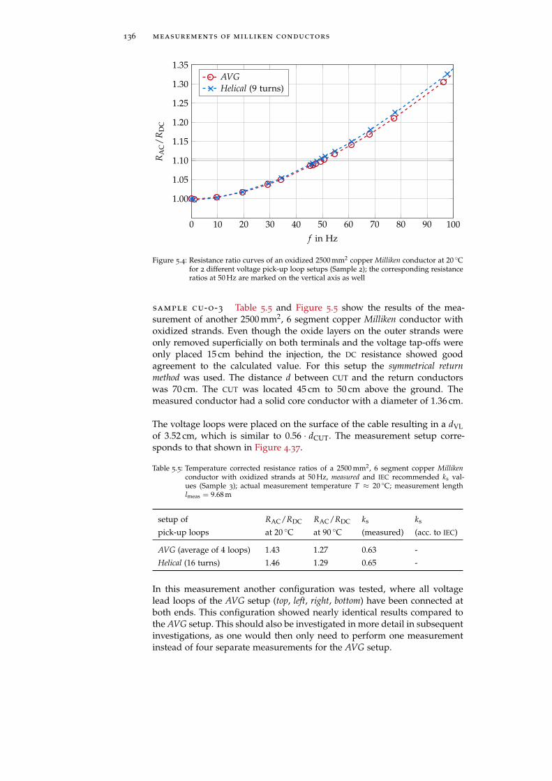
136 measurements of milliken conductors
0 10 20 30 40 50 60 70 80 90 100
1.00
1.05
1.10
1.15
1.20
1.25
1.30
1.35
f in Hz
RAC/RDC
AVGHelical (9 turns)
[ July 10, 2018 at 13:44 – Draft PhD thesis Suchantke ]
Figure 5.4: Resistance ratio curves of an oxidized 2500 mm2 copper Milliken conductor at 20 Cfor 2 different voltage pick-up loop setups (Sample 2); the corresponding resistanceratios at 50 Hz are marked on the vertical axis as well
sample cu-o-3 Table 5.5 and Figure 5.5 show the results of the mea-surement of another 2500 mm2, 6 segment copper Milliken conductor withoxidized strands. Even though the oxide layers on the outer strands wereonly removed superficially on both terminals and the voltage tap-offs wereonly placed 15 cm behind the injection, the DC resistance showed goodagreement to the calculated value. For this setup the symmetrical returnmethod was used. The distance d between CUT and the return conductorswas 70 cm. The CUT was located 45 cm to 50 cm above the ground. Themeasured conductor had a solid core conductor with a diameter of 1.36 cm.
The voltage loops were placed on the surface of the cable resulting in a dVLof 3.52 cm, which is similar to 0.56 · dCUT. The measurement setup corre-sponds to that shown in Figure 4.37.
Table 5.5: Temperature corrected resistance ratios of a 2500 mm2, 6 segment copper Millikenconductor with oxidized strands at 50 Hz, measured and IEC recommended ks val-ues (Sample 3); actual measurement temperature T ≈ 20 C; measurement lengthlmeas = 9.68 m
setup of RAC/RDC RAC/RDC ks ks
pick-up loops at 20 C at 90 C (measured) (acc. to IEC)
AVG (average of 4 loops) 1.43 1.27 0.63 -
Helical (16 turns) 1.46 1.29 0.65 -
In this measurement another configuration was tested, where all voltagelead loops of the AVG setup (top, left, right, bottom) have been connected atboth ends. This configuration showed nearly identical results compared tothe AVG setup. This should also be investigated in more detail in subsequentinvestigations, as one would then only need to perform one measurementinstead of four separate measurements for the AVG setup.

5.1 measurement of different conductor designs 137
0 10 20 30 40 50 60 70 80 90 1001.0
1.2
1.4
1.6
1.8
2.0
2.2
f in Hz
RAC/RDC
AVGHelical (16 turns)
[ July 10, 2018 at 13:42 – Draft PhD thesis Suchantke ]
Figure 5.5: Resistance ratio curves of an oxidized 2500 mm2 copper Milliken conductor at 20 Cfor 2 different voltage pick-up loop setups (Sample 3); the corresponding resistanceratios at 50 Hz are marked on the vertical axis as well
5.1.2.3 Enameled
sample cu-e Table 5.6 and Figure 5.6 show the results of the mea-surement of a 2500 mm2, 6 segment copper Milliken conductor withunidirectional pitch and enameled wires. The DC resistance showed goodagreement to the calculated value. For this setup the sheath return methodwas used. The sheath consisted of a copper wire screen in combinationwith an aluminum sheath. The CUT was located at more than 1 m above thelaboratory floor. The measured conductor had no core conductor.
The voltage loop was placed on the surface of the cable resulting in a dVLof 3.9 cm, which is similar to 0.56 · dCUT. At the time of the measurementit was not possible to perform the AVG setup. Moreover, the measurementlength was only 3 m. The measurement setup corresponds to that shown inFigure 4.37 but only using one helical voltage loop.
Table 5.6: Temperature corrected resistance ratios of a 2500 mm2, 6 segment copper Millikenconductor with enameled strands at 50 Hz, measured and IEC recommended ks values;actual measurement temperature T = 23.82 C; measurement length lmeas = 3 m
setup of RAC/RDC RAC/RDC ks ks
pick-up loops at 20 C at 90 C (measured) (acc. to IEC)
Helical (4 turns) 1.220 1.126 0.38 0.35
The results show a slight upward deviation from the IEC standard. Neverthe-less, the measurement length was only 3 m and as discussed in more detailin Section 4.2.5, it is questionable how the measurement length affects theresults. Longer samples may perform differently.

138 measurements of milliken conductors
0 10 20 30 40 50 60 70 80 90 100
1.0
1.1
1.2
1.3
1.4
1.5
1.6
1.7
1.8
f in Hz
RAC/RDC
Helical (4 turns)
[ July 10, 2018 at 13:40 – Draft PhD thesis Suchantke ]
Figure 5.6: Resistance ratio curves of an enameled 2500 mm2 copper Milliken conductor at 20 C;the corresponding resistance ratio at 50 Hz is marked on the vertical axis as well
5.2 comparison to iec standard and discussion of results
All measurement results are plotted again in Figure 5.7 and compared tothe IEC recommendation. It was already apparent in every section that thepresented results differ from the IEC standard.
0 500 1000 1500 2000 2500 3000 3500
1.0
1.2
1.4
1.6
1.8
2.0
2.2
cross section A in mm2
RAC/RDC
Cu ks = 1.00Cu ks = 0.80Cu ks = 0.62Cu ks = 0.435Cu ks = 0.35Al ks = 0.25Al (AVG)CU-B (AVG)CU-O-1 (AVG)CU-O-2 (AVG)CU-O-3 (AVG)CU-E (Helical)
[May 9, 2018 at 14:27 – Draft PhD thesis Suchantke ]
Figure 5.7: Resistance ratios at 50 Hz plotted over conductor cross section for different ks fac-tors at 20 C according to IEC standard 60287-1-1:2006/AMD1:2014 including theresults of the ks factor measurements; the colors and styles of the markers showtheir belonging to the ks factor; there is no recommendation for oxidized samplesfrom the IEC

5.2 comparison to iec standard and discussion 139
The following things can be concluded from the measurement results com-pared to the IEC standard recommendation:
I the aluminum conductor (Al) performed worse than expected;
I the blank copper conductor (CU-B), which experienced 88 heat cycles,performed better;
I the oxidized conductor CU-O-1 performed similar to the IEC recom-mendation for a copper Milliken conductor with unidirectional pitch;
I the oxidized conductor CU-O-2 performed even better than the recom-mendation for an enameled design;
I the oxidized conductor CU-O-3 also performed similar to the IEC
recommendation for a copper Milliken conductor with unidirectionalpitch;
I the enameled conductor (CU-E) performed slightly worse, where themeasurement length was only 3 m however and may have influencedthe outcome.
Again, these results should not be used to rate different Milliken conduc-tor designs. The performance of each design strongly depends on themanufacturing process and quality and can vary for every other sampleand maybe even along the sample length. Moreover, many other designchoices influence the results. The consequence of these results is that an AC
resistance measurement should be performed in any case, as the results candiffer significantly from the recommendation by the IEC standard.
Figure 5.8 shows all measurement results up to a frequency of 300 Hz.
0 50 100 150 200 250 300
1
2
3
4
f in Hz
RAC/RDC
Al (AVG)CU-B (AVG)CU-O-1 (AVG)CU-O-2 (AVG)CU-O-3 (AVG)CU-E (Helical)
[ July 10, 2018 at 13:47 – Draft PhD thesis Suchantke ]
Figure 5.8: Resistance ratio of all measurements up to 300 Hz at 20 C
Extended investigations on different Milliken conductor designs showedlarge deviations from the Bessel function, used for a cylindrical isolatedconductor, at frequencies between 300 Hz and 1000 Hz. This is expected asmultiple insulated conductors interacting with each other will introduce

140 measurements of milliken conductors
higher order Bessel functions [Dwi23a]. The curves look similar to the onesshown for litz wires in [Alb17, Abb. 4.28] but already far below 1000 Hz.
What could also be observed in measurements is that in all cases, wherethe sheath return method was used, outer magnetic fields existed. Largerloops still affected the results, more specifically the reactance and resistance.In turn this means that the setup was not perfectly concentric, eithergeometrically or from the current distribution point of view. Only thiscondition could suppress outer fields as discussed earlier. But, due toallowed asymmetries in the sheath design, this was also expected from theprevious findings.
Helical voltage loops with many turns showed good agreement to AVG. Inall cases the deviation of the helical configuration to the AVG setup wassmaller than the maximum differences between the separate pick-up loops(top, left, bottom, right) at 50 Hz.

6C O N C L U S I O N
I think and think for months and years.Ninety-nine times, the conclusion is false.
The hundredth time I am right.Albert Einstein
This chapter summarizes the outcomes of this thesis. First the main resultsof each chapter are concluded. Some of them are then further discussed.At the end, the limits of this thesis are shown and a recommendation forfurther research is given in the outlook.
6.1 summary
The main purpose of this work was to research, if and how an accurateAC loss measurement can be performed on power cables with large crosssections using the electrical measurement method.
Chapter 1 introduces the underlying problematic and defines the targetvalue of this thesis, the isolated Joule losses of the inner conductor of apower cable. Then, the recent standards for power cable ratings are pre-sented, which recommend the measurement of the AC resistance, but alsoprovide empirical formulas for the AC resistance calculation. Afterwards,available measurement methods are presented, namely the calorimetricmethod and different electrical measurement methods. The latter is used inthis work as it offers logistical advantages over the calorimetric approach.At the end of Chapter 1, the need for accurate AC resistance measurementsis outlined again, by showing how AC losses can vary due to manufacturingquality. The measurement is of great importance, as the AC resistance of acable is a critical parameter for the design of a cable system.
Chapter 2 describes the used measurement system in detail after listingsome definitions and important terms at the beginning. It could be shownthat the accuracy of the used system is high enough to distinguish differentrelevant effects in the measurement. It is then demonstrated how measure-ment values are interpolated and also how they are corrected to a desiredtemperature for evaluation. This is followed by reviewing the used simu-lation technique: the FEM in Comsol Multiphysics. Chapter 2 is concludedwith a short overview and comparison of the available methods for thedetermination of Joule losses of a conductor. It is best to combine analyticalformulas, simulations—such as the FEM—and measurements to obtain re-search results that come as close as possible to the true losses of a conductor.
Chapter 3 first presents some milestones of the research on AC lossesand reasons that the MQS approximation can be used for the subsequentinvestigations. After a description of skin effect and proximity effect, somefurther concepts of AC loss mechanisms are introduced. A revised collectionof analytical formulas is presented in detail and followed by some approxi-mate formulas and a comparison of current distribution and AC resistances

142 conclusion
of different cross sectional shapes. At the end, Chapter 3 displays thedevelopment and structure of power cable conductors, specifically strandedand Milliken conductors. Using copper as the conductor material, the lattercan be subdivided into three different designs: blank, oxidized or enameledstrands and is able to reduce AC losses significantly.
Chapter 4 points out what is actually being measured using an ADC AC
voltmeter. At AC, it is the total electric field intensity over the internalmeasurement resistance, which is composed of the line integral of theelectric field between both voltage tap-offs on the CUT and an inductivepart caused by the alternating magnetic field present in the pick-up loop.In case of complex cross sectional conductor shapes or if other conductiveparts are nearby, this magnetic field can become complex and influencethe measured resistive voltage drop. The resistance measurement thendepends on the location and geometric dimension of the pick-up loop. Itwas shown that all complex magnetic fields originating from the CUT haveto be included in the voltage pick-up loop to account for the true lossesof the CUT. Most important, even for insulated conductors the electricalmeasurement method is able to obtain the overall true losses of a conductorsection, through the information stored in the complex magnetic field inthe pick-up loop. For stranded and segmental conductors, whose currentdensity distribution is expected of being nearly rotationally symmetric,the necessary radial extension of the pick-up loop—to capture sufficientcomplex magnetic field—is expected to be achieved at a distance identicalto the diameter of the CUT. For typical measurement setups it was thenshown that it is easy to avoid an influence of the return conductor onthe true losses of the CUT, by increasing the spacing between both. Forthese setups, measured losses were compared to the true losses of theCUT for different positions of the pick-up loops. It could be shown thattaking the average of 4 pick-up loops homogeneously arranged around thecircumference of a CUT, delivers results of sufficient accuracy in every setupeven for small loop sizes. Current homogenization and the placement of thevoltage tap-offs are closely related. From the investigations performed, itwas inferred that for the measurement, the terminals of a power cable withinsulated strands should be blank. This has the advantage of enabling quickcurrent homogenization along the conductor axis—which is a necessaryrequirement for representative results—on one hand and at the same timeprovide a defined position for the voltage tap-offs. With this, one avoidshaving to connect the voltage tap-offs to the exact same strand at bothterminals. In practice however, it is often sufficient to check, if the methodused for current injection and the position of the voltage tap-offs deliver theexpected DC resistance. If this is the case, the chosen method is adequatefor the AC resistance measurement as well. At the end of Chapter 4 arecommendation for preparation of the CUT, setup and procedure for theAC loss measurement is given. Using two symmetrical return conductorswith a spacing larger than 0.5 m in combination with averaging the resultsobtained by 4 pick-up loops located at the surface of the cable, leads toresults, which are sufficiently close to the true resistance of a Millikenconductor.
Chapter 5 shows measurement results of some Milliken conductor designs,which were obtained by applying the recommended techniques. It wasshown that the measured values often did not coincide with the values

6.2 discussion and outlook 143
recommended by the recent IEC standard. This supports the demand forperforming AC resistance measurements on power cable conductors toensure that the expected or required AC resistance is met.
6.2 discussion and outlook
comments on methodology and performed investigationsFor the simulations performed in this thesis the well-established FEM tech-nique was used. Comparisons with different analytical solutions showed theexcellent agreement between both. For simple conductor shapes—such as acircular cross section—both results could also be verified by measurement.At the moment, a measurement is the only reliable approach to determinethe AC resistance of a Milliken conductor, if performed properly. It ishence reasonable to benchmark the measurement by analytical calculationsand FEM simulations prior to measurements of Milliken conductors. Inpractice, analytical solutions and the FEM are no suitable methods for the AC
resistance determination of a Milliken conductor. True 3D FEM simulationsof segmental conductors are not feasible at the moment due to restrictionsin hardware resources and the lacking knowledge of some manufacturinginfluences on the design. The simulations of different measurement setupsin this thesis therefore used a solid circular copper conductor as the CUT. Itwas shown that in general stranded conductor designs have lower proximityeffect losses compared to solid conductors. Even though stranded andMilliken conductors still show proximity effect [Joa99], the results displayedin this thesis therefore possibly show stronger impacts on the measurementthan present in a real measurement. On the other hand, asymmetries in thegeometry of the setup and unknown factors from real setups, such as theexact geometry and electrical properties of laboratory floors or walls havingrebars for example, could only be included in the simulations exemplarily. Aprevious example showed that a metallic fence placed 2 m from the CUT stillsignificantly influenced the measurement of a rectangular conductor. Alsodeviations from the symmetric placement of the pick-up loops relative tothe setup were not part of the investigations either. In addition to that, somepossible geometric variations caused by the manufacturing process like oval-ity of the cable or the displacement of segments were not researched as well.
To differentiate between different effects in the measurement, possiblegeometric variations have mostly been analyzed separately. In reality, mul-tiple effects could act upon the measurement at once, having stronger ordifferent influences on the pick-up loops than indicated by the simulations.Nevertheless, using at least 4 pick-up loops to average the results showed tobe a quite robust method against geometric asymmetries. It is also evidentthat in reality not every pick-up loop configuration shown in the simulationresults can be realized in practice. For example when measuring a cable,one cannot simply place the voltage lead wires beneath the sheath. Also incase of Setup III—symmetric return method—the voltage pick-up loops on thesides of the closely spaced return conductors can of course not be routedthrough the return conductors. In Appendix A.2 it is shown that this doesnot present a limitation for the AVG setup. To resolve this issue, all pick-uploops or the return conductor can be rotated relative to the center of theCUT still delivering accurate results.

144 conclusion
One additional remark about the AVG setup concerns the positioning ofthem on cables. The radial distance of the voltage loops dVL is defined fromthe surface of the CUT. When analyzing apparent losses for the evaluationof the average value, the results at the same distances were used. But, theexact position of the CUT in a cross section of a cable is not known exactlydue to eccentricity. Hence, the pick-up loops attached to the surface ofthe complete cable may have different distances dVL to the surface of theCUT. Hence in reality, the AVG is maybe comprised of top(dVL), bottom(dVL),right(dVL + 2 mm) and left(dVL − 2 mm). When looking at the changein every setup for distances of 2 mm—which is the allowed maximumeccentricity—one can see that the error introduced by that is negligible.
When the measured resistance has to be evaluated at a different temperaturethan it was measured at, the resistance has to be adjusted. A way of doingthat was shown in Section 2.4.2. It is based on the observation that differenttemperatures also change the conductivity of the sample. The conductivityin turn influences its AC losses. Hence, the ratio of AC to DC resistancechanges with temperature. If geometric parameters of the conductorremain unchanged, this method can accurately correct the resistance frommeasurement temperature to the desired evaluation temperature. But, incase of conductors with insulated wires it is not clear at the moment if theinterwire contact resistances also vary at higher temperatures. If so, thiscould equal a change in geometry. Assuming that the interwire resistancesdecrease with temperature, would turn a conductor with insulated wiresinto a solid conductor, which increases AC losses in return.
In publications authors should describe their setup in every detail, to in-crease reproducibility and classification of the presented results of Millikenconductor measurements. Especially the influence of the position of the volt-age pick-up loop should be discussed more deeply.
comments on the measurement results It was not possible tofollow every recommendation in all measurements shown in Chapter 5.Some measurements were already performed parallel to open investiga-tions. Nevertheless, additional FEM simulations for these specific setups andcomparisons of possible influences to measurements performed accordingto the recommendation, helped increasing the trust in the results shown.For every measurement it was described in detail how the setup was buildto increase transparency. Moreover, even though the results are of highaccuracy, their only purpose is to give examples of the performance ofdifferent designs, as they only present a small empirical sample for thisdesign type (blank, oxidized, . . . ). Samples of different manufacturershaving the same design, can differ significantly in performance as arguedpreviously.
Concerning the positioning of the voltage tap-offs it was often sufficient inthe measurement to place the voltage tap-offs 0.5 m to 2 m away from thecurrent injection on the blank surface of the segments. The calculated DC
resistance was met even in enameled designs, where the current was onlyinjected into one strand at the terminals. This means that many interwirecontact resistances were present to guarantee the homogenization over allstrands. Methods like this can therefore be used to check the functionalityof the design itself. Nevertheless, the exact DC resistance of a Milliken

6.2 discussion and outlook 145
conductor can also not be calculated in advance as the exact helical pathsof the strands and possible contacts between them are unknown.
Moreover, it was stated by some manufacturers that the cable geometry andperformance of the CUT can vary along the whole cable and can be uniquefor every section. Assuming these variations are significant, this wouldmean that multiple short samples of a production length have to measuredto obtain a result of statistical relevance. This however does not seem tobe realizable in practice. This issue is similar to the topic of MinimumNecessary Measurement Length and presents a general challenge for everymeasurement method. Both issues can only be resolved when the completeproduction length is measured. This observation seems to increase thedemand for a measurement on a cable drum, which does not seem feasibleat the moment due to the inclusion of proximity effect and magnetic strayfields on the drum, which is often metallic because of mechanical con-straints. In addition to that, it is also not clear how drumming and bendingof the cable affects the performance, more specifically the insulation ofthe single strands of Milliken conductors. A measurement of the completemanufacturing length when buried on site would deliver the most accurateresult. Despite considerations on how to realize such a measurement setup,this is also not a desired solution. If the measurement would deliver an AC
resistance, which does not meet the demanded requirements, this wouldhave to result in an exchange of the already buried cable.
A better solution would be to come as close as possible to the true resistanceby measuring short samples in the laboratory, after performing additionalinvestigations on Milliken conductors, which clarify the influence of the ef-fects discussed above.
outlook This section is based on the discussion and presents ideas onfurther research, which is necessary—in the eyes of the author—to increasetrust and accuracy of AC resistance measurements.
This includes the following:
I A comparison of electrical measurement methods and the calorimetricmeasurement method. Even though both techniques are used in prac-tice, a direct comparison on a Milliken conductor at different temper-atures is desired. This includes an estimate on the accuracy of bothmethods. Compliance of the measurement results would boost thetrust in both methods and help the user to focus on the advantagesof the approaches only, when selecting an appropriate method.
I For the same reason, a comparison of the typically used electrical mea-surement methods should be performed: using lock-in amplifiers onone hand and using AC ADC voltmeters on the other hand.
I The enunciated temperature correction method should be checked forapplicability on Milliken conductors by performing measurement atdifferent temperatures. This would answer the question of whetherthe insulation of the single wires is affected by temperature changes.This question needs to be answered for different conductor materialsand designs.

146 conclusion
I The remaining parameters influencing the measured resistance shouldbe checked for their influence. This can be done by FEM simulationsand includes:
– The ovality of a cable and of the inner conductor.
– The displacement of segments in Milliken conductors.
– The losses induced in the pick-up loops by armored cablesheaths.
I Different lengths of conductor samples should be measured to checkfor the influence of the length upon the AC resistance.
I Also, the effect of drumming the cable should be investigated empir-ically by measuring a conductor before and after it has been on adrum. This should also be done with different designs, as the mechan-ical stress can possible influence enameled wires differently comparedto oxidized strands for example.
I Further investigations regarding the AC resistance measurement on adrum are required to check if measuring a whole production lengthmay be possible under certain conditions or using special precautions.
I Further theoretical considerations, FEM simulations and measurementscould justify or reject the idea of using only one helically wound volt-age loop instead of 4 voltage loops, whose results are averaged. Thiscould save time and increase efficiency of the electrical method fur-ther. The idea of using the cable sheath as the rear voltage lead wireshould also be investigated further together with the possibility ofshort-circuiting all 4 loops of the AVG setup on both sides.
I Long-term behavior of conductors with insulated strands should alsobe investigated, as thermal induced mechanical stress can possibly re-duce interwire resistances and increase losses over the lifetime of acable. Nevertheless, for blank conductors oxidization of the strandscould also appear and increase the performance in long-terms.

AA D D I T I O N A L C O N T E N T
No man has the right to be an amateur in the matter ofphysical training. It is a shame for a man to grow old without
seeing the beauty and strength of which his body is capable.Socrates
a.1 published results of milliken conductor measurements
Regarding Table A.1: the ks factor could not be calculated in most cases be-cause often the DC resistance or lengths was not available. Moreover, if no fre-quency was given, the typical power frequency of the country, where the in-vestigation was performed was assumed. If no temperature was given in thereference, then 20 C was used and the “operating temperature” in [BM68]was assumed to be 90 C. “Dis” in the reference stands for discussion, “4s”stands for 4 segments and so forth, “hp” stands for high pressure, “lp” forlow pressure, “contra.” stands for contradirectional and “uni.” for unidirec-tional stranding of the different layers.
Table A.1: Collection of published RAC/RDC ratios for Milliken conductors (no proximity effectregarded)
A in material design/ f in T in RAC/RDC reference
mm2 insulation Hz C
1015 Al blank 60 23 1.02 [Kat+78]
1015 Cu blank 60 23 1.13 [Kat+78]
1015 Cu blank 60 23 1.16 [Kat+78]
1015 Cu blank 60 23 1.06 [Kat+78]
1015 Cu blank 60 23 1.08 [Kat+78]
1015 Cu blank 60 23 1.09 [Kat+78]
1015 Cu enameled 60 23 1.05 [Kat+78]
1015 Cu lead alloy 60 23 1.07 [Kat+78]
1015 Cu lead alloy 60 23 1.09 [Kat+78]
1015 Cu lead alloy 60 23 1.08 [Kat+78]
1015 Cu tin 60 23 1.06 [Kat+78]
1200 Cu blank 50 20 1.15 [Cig05, p. 14]
1269 Cu blank 60 20 1.113 [Wis48]
1269 Cu blank 60 23 1.2 [Kat+78]
1269 Cu blank 60 23 1.1 [Kat+78]
1269 Cu blank 60 23 1.08 [Kat+78]
1269 Cu blank 60 23 1.07 [Kat+78]
1269 Cu blank 60 80 1.07 [Wis48]
1400 Al blank 50 90 1.05 [BM68]
1400 Cu blank 50 20 1.18 [Cig05, p. 14]

148 additional content
1400 Cu blank, contra. 50 90 1.18 [BM68]
1400 Cu blank, uni. 50 90 1.13 [BM68]
1400 Cu enameled 50 90 1.07 [BM68]
1400 Cu sulphurated 50 90 1.15 [BM68]
1600 Cu blank 50 20 1.23 [Cig05, p. 14]
1600 Cu blank 50 20 1.04 [CMR77, Dis]
1600 Cu blank 50 90 1.25 [DM07]
1600 Cu blank (4s) 50 18 1.34 [BSF99]
1600 Cu blank (5s) 50 27 1.11 [BSF99]
1600 Cu blank (6s) 50 33 1.25 [BSF99]
1600 Cu enameled 50 20 1.03 [Cig05, p. 14]
1600 Cu enameled 50 90 1.04 [DM07]
1600 Cu enameled (6s) 50 26 1.02 [BSF99]
1600 Cu oxidized 50 20 1.07 [Cig05, p. 14]
1776 Cu tin 60 23 1.17 [Kat+78]
1920 Cu blank 50 20 1.33 [Cig05, p. 14]
2000 Al blank, contra. 50 80 1.025 [CMR77]
2000 Al blank, contra. 50 80 1.026 [CMR77]
2000 Cu blank 50 20 1.34 [Cig05, p. 14]
2000 Cu blank 50 20 1.27 [Cig05, p. 14]
2000 Cu blank 50 20 1.24 [Cig05, p. 14]
2000 Cu blank 50 20 1.378 [RSS11a]
2000 Cu blank 50 20 1.328 [RSS11a]
2000 Cu blank 50 20 1.495 [RSS11a]
2000 Cu blank 50 20 1.448 [RSS11a]
2000 Cu blank 50 80 1.16 [Joa98, p. 55]
2000 Cu blank 50 80 1.23 [Joa98, p. 55]
2000 Cu blank 50 80 1.232 [Joa98, p. 55]
2000 Cu blank 50 85 1.359 [RSS11a]
2000 Cu blank 50 90 1.35 [DM07]
2000 Cu blank 50 90 1.352 [RSS11a]
2000 Cu blank, contrad. 50 80 1.25 [CMR77]
2000 Cu Cr-plated, contra. 50 80 1.15 [CMR77]
2000 Cu enameled 50 20 1.04 [Cig05, p. 14]
2000 Cu enameled 50 90 1.04 [DM07]
2000 Cu enameled, contra. 50 80 1.1 [CMR77]
2000 Cu enameled, contra. 50 80 1.05 [CMR77]
2000 Cu oxidized (hp) 50 80 1.137 [Joa98, p. 55]
2000 Cu oxidized (lp) 50 80 1.086 [Joa98, p. 55]
2072 Cu blank 50 20 1.568 [RSS11a]
2385 Al blank 60 23 1.05 [Kat+78]
2500 Cu blank 50 20 1.36 [Cig05, p. 14]
2500 Cu blank 50 80 1.2 [Joa98, p. 57]
2500 Cu blank 50 90 1.45 [DM07]
2500 Cu blank, contra. 50 80 1.232 [Joa98, p. 57]

A.2 extended discussion on ac loss measurements 149
2500 Cu enameled 50 20 1.02 [Cig05, p. 14]
2500 Cu enameled 50 90 1.065 [DM07]
2500 Cu oil impregnated 50 80 1.14 [Joa98, p. 57]
2500 Cu oil impregnated 50 80 1.151 [Joa98, p. 57]
2500 Cu oxidized 50 20 1.08 [Cig05, p. 14]
2500 Cu oxidized (hp) 50 80 1.23 [Joa98, p. 57]
2500 Cu oxidized (lp) 50 80 1.152 [Joa98, p. 57]
2600 Cu blank 50 20 1.1 [CMR77, Dis]
a.2 extended discussion on ac loss measurements
Figure A.1 presents results of the virtual measurement on an hypotheticalconductors with 4 insulated strands and two solid terminals. The currentflows in z-direction and is homogeneously injected at both terminals.
Both models shown, consist of two solid terminals with an overall radiusr ≈ 2.8 cm and 4 strands in between them, which are insulated fromone another by air. The current is injected into the face of one terminal,whereas the other terminal’s cross section is grounded. In Model 1, allstrands are electrically connected to both terminals. Therefore, the currentflows from one terminal to the other over all strands. In Model 2, there is asmall gap between the strand at the bottom side and the rearward terminal.Therefore, the measurement current will not flow through this strand fromone terminal to the other. Nevertheless, eddy currents will build up in thisstrand due to the alternating electromagnetic fields from the other strands.
The measured resistance will eventually converge against the true resistanceof the measured section in both cases. For Model 2 this means that thelosses due to eddy currents in the bottom strand are also included. One cansee that due to the large asymmetry of the models, dVL,min, which is thedistance to reach a deviation smaller than 1 % to the true resistance, is muchlarger than 3 × r ≈ 8.4 cm in this case.
Another interesting case is that of two closely spaced conductors:
I If the conductors are connected in a return circuit, the measured resis-tance will converge against the true resistance of only this conductor,to which the voltage tap-offs are attached to (the CUT). Losses from thereturn conductors will not be included at very large dVL anymore.
I If the conductors are in a go circuit—connected in parallel—the mea-sured resistance converges against the true resistance of the measuredsection with increasing dVL, which includes the losses of both conduc-tors. This is consistent and also observed in the example of the 4 strandbundle above. For 2 unequal conductors, the separation of losses is acomplex task (see Section 4.4.3).
In both cases, taking the average of the 4 pick-up loops le f t, right, top andbottom will converge against the true resistance much quicker, than any ofthe above configurations separately. As long as the 4 pick-up loops are dis-tributed homogeneously around the CUT’s circumference (every 90° result-ing in le f t, right, top and bottom), independent of the relative position of

150 additional content
the return conductor, by using the AVG setup the result quickly convergesagainst the true losses of the CUT only.
z
y
x
dVL
I
(a) Model 1: all 4 strands are connectedthrough, pick-up loop in blue
void
(b) Model 2: the bottom strand is not con-nected through, pick-up loop in blue
(c) Model 1 - ||J|| in the center plane (d) Model 2 - ||J|| in the center plane
0 10 20 30250
300
350
dVL in cm
RACin
µΩ/m
RvirtRtrue
0 10 20 30250
300
350
dVL in cm
RACin
µΩ/m
RvirtRtrue
[ April 28, 2018 at 11:24 – Draft PhD thesis Suchantke ]
(e) left: convergence of virtual resistance in model 1; right: convergence of virtual resistancein model 2
Figure A.1: Results of additional investigations on stranded conductors; Rtrue are the overalllosses in all small strands only (middle section); the simulation was performedat 500 Hz, the terminals for current injection have a cross section of 2500 mm2; thesmall strands have a radius of 2.5 mm; the coordinate system in Figure A.1a is validfor all other figures as well

BM AT L A B C O D E F O R A N A LY T I C A L F O R M U L A S
Greatness is not a measure of how great you arebut how great others came to be because of you.
Cus D’Amato
The results obtained with the following Matlab codes have been tested andverified by comparison with FEM simulations in Comsol Multiphysics.
b.1 infinitively wide strip
Listing B.1: Matlab code for the resistance caluclation of an infinitively wide strip
% Script to calculate the current density,
% resistancea and reactance ratio of an
% Infinitively Wide Strip
% Date: 2016-10-20 - 12:40 / Author: Rene Suchantke
% Constants
mu_0 = 4*pi*1E-7 ; % vacuum permability
% Input Parameters
f = 0:1:300 ; % frequency / Hz
sigma = 58E6 ; % conductivity / S/m
t = 0.02 ; % thickness of strip / m
mu_r = 1 ; % permeability
% Calculation of Variables
y = -t/2:t/100:t/2 ; % generation of y-coordinate
omega = 2*pi.*f ; % angular frequency / Hz
% Conversion to cgs units for use in orignal formulas
sigma = sigma/(1E11) ; % [S/m]-->[abmhos/cm]=[GS/cm]
t = t*100 ; % [m]-->[cm]
y = y*100 ; % [m]-->[cm]
% Calculation of alpha
alpha = sqrt(2*pi*sigma.*omega*mu_r)...
+(1i*sqrt(2*pi*sigma.*omega*mu_r));
% Current Density at 50 Hz normalized to the surface current density
J_ratio = cosh(alpha(51).*y)/cosh(alpha(51)*(t/2));
% Resistance Ratio
R_ratio = real((alpha*t)./...
(2*tanh((alpha*t)/2)));
R_ratio(1) = 1;
% Reactance Ratio
X_ratio = imag((alpha*t)./...
(2*tanh((alpha*t)/2)));

152 matlab code for analytical formulas
b.2 solid cylindrical conductor
Listing B.2: Matlab code for the resistance caluclation of a solid cylindrical conductor
% Script to calculate the current density,
% resistancea and reactance ratio of a
% Solid Cylindrical Conductor
% Date: 2016-10-01 - 13:56 / Author: Rene Suchantke
% Constants
mu_0 = 4*pi*1E-7 ; % vacuum permability
% Input Parameters
f = 0:1:1000 ; % frequency / Hz
sigma = 58E6 ; % conductivity / S/m
r_c = 0.02 ; % conductor radius / m
mu_r = 1 ; % permeability
I = 1 ; % conductor current / A
% Calculation of Variables
r = -r_c:r_c/100:r_c ; % generation of r-coordinate
omega = 2*pi.*f ; % angular frequency / Hz
R_DC = 1/(sigma*pi*r_c^2); % DC resistance / Ohm/m
L_DC = mu_0*mu_r/(8*pi) ; % DC inductance / H/m
% Calculation of Function Argument m
m = sqrt(-1i*omega*mu_0*mu_r*sigma);
% Current Density at 50 Hz Normalized to the DC Current Density
% by using the Bessel Function of the First Kind
J_AC = (m(51)*I/(2*pi*r_c))*(besselj(0,m(51)*r)./...
besselj(1,m(51)*r_c));
J_DC = I/(pi*r_c^2); % DC current density / A/m^2
J_ratio = real(J_AC)/J_DC; % current density ratio(50Hz)
% Resistance Ratio Calculated with Bessel Function of the First Kind
R_ratio = real(((m*r_c/2).*besselj(0,m*r_c)./besselj(1,m*r_c)));
R_ratio(1)= 1;
% Inductance Ratio Calculated with Bessel Function of the First Kind
L_ratio = (R_DC*8*pi./(omega.*mu_r*mu_0)).*...
imag(((m*r_c/2).*besselj(0,m*r_c)./besselj(1,m*r_c)));
L_ratio(1) = 1;
%% Additional Verification with Kelvin Function Formulas
k = real(m)*sqrt(2); % argument of Kelvin functions
% Generating the Kelvin Functions and Their Derivatives
v = 0; % Order of Kelvin functions
ber_v = real(besselj(v,k*r_c*exp(1i*3*pi/4))); % Generating Ber
bei_v = imag(besselj(v,k*r_c*exp(1i*3*pi/4))); % Generating Bei
berD_v = (real(besselj(v+1,k*r_c*1i*sqrt(1i)))+...
imag(besselj(v+1,k*r_c*1i*sqrt(1i))))/sqrt(2)+...
(v./k).*real(besselj(v,k*r_c*1i*sqrt(1i)));% Generating Ber’
beiD_v = (imag(besselj(v+1,k*r_c*1i*sqrt(1i)))-...
real(besselj(v+1,k*r_c*1i*sqrt(1i))))/sqrt(2)+...
(v./k).*imag(besselj(v,k*r_c*1i*sqrt(1i)));% Generating Bei’
% Resistance Ratio Calculated with Bessel Function of the First Kind
R_ratio_V = k*r_c/2.*...
((ber_v.*beiD_v)-(bei_v.*berD_v))./(berD_v.^2+beiD_v.^2);
R_ratio_V(1) = 1;
% Reactance Ratio Calculated with Bessel Function of the First Kind
L_ratio_V = (R_DC*8*pi./(omega.*mu_r*mu_0)).*...
k*r_c/2.*((ber_v.*berD_v)+(bei_v.*beiD_v))./(berD_v.^2+beiD_v.^2);
L_ratio_V(1) = 1;
% Principle of Similitude Parameter

B.3 tubular conductor 153
p = sqrt(f/R_DC).*1e-3;
R_AC_50 = R_ratio(51)*R_DC
X_AC_50 = L_ratio(51)*L_DC*2*pi*f(51)
b.3 tubular conductor
Listing B.3: Matlab code for the resistance caluclation of a tubular conductor
% Script to calculate the current density,
% resistancea and reactance ratio of a
% Tubular Conductor
% Date: 2017-01-10 - 17:56 / Author: Rene Suchantke
% Constants
mu_0 = 4*pi*1E-7 ; % vacuum permability
% Input Parameters
f = 0:1:1000 ; % frequency / Hz
sigma = 58E6 ; % conductivity / S/m
r2 = 0.025; % outer conductor radius / m
r1 = 0.0125; % inner conductor radius / m
A = pi*(r2^2-r1^2); % cross section / m^2
mu_r = 1 ; % permeability
% Calculation of Variables
omega = 2*pi.*f ; % angular frequency / Hz
R_DC = 1/(A*sigma) ; % DC resistance / Ohm/m
% Definition of variables according to AC calculation formula
k = sqrt(2*pi*f*mu_r*mu_0.*sigma);
% Creation of Kelvin function arguments
kr_1 = k*r1;
kr_2 = k*r2;
% Current Density: Import of Comsol Results
r = -r2:2*r2/192:r2 ; % generation of r-coordinate
fileID =fopen( ’Tube50Hz. txt ’, ’ r ’);formatSpec = ’%f %f ’;B = fscanf(fileID,formatSpec);
n = 1;
for i=1:2:length(B)-1
J_ratio(n)=B(i+1);
rn(n) =B(i);
n = n+1;
end
% creating the kelvin functions with argument mr_1:
v = 0; % Order of the functions
ber_mr1 = real(besselj(v,kr_1*exp(3*pi*1i/4)));
bei_mr1 = imag(besselj(v,kr_1*exp(3*pi*1i/4)));
ker_mr1 = real(exp(-v*pi*1i/2)*besselk(v,kr_1*exp(pi*1i/4)));
kei_mr1 = imag(exp(-v*pi*1i/2)*besselk(v,kr_1*exp(pi*1i/4)));
% creating their derivatives - taken from:
v = 1; % Order of the functions
ber_mr1_diff1 = (real(besselj(v,kr_1*1i*sqrt(1i)))+...
imag(besselj(v,kr_1*1i*sqrt(1i))))/sqrt(2);
bei_mr1_diff1 = (imag(besselj(v,kr_1*1i*sqrt(1i)))-...
real(besselj(v,kr_1*1i*sqrt(1i))))/sqrt(2);
ker_mr1_diff1 = ( real(exp(-v*pi*1i/2)*besselk(v,kr_1*exp(pi*1i/4)))
+...

154 matlab code for analytical formulas
imag(exp(-v*pi*1i/2)*besselk(v,kr_1*exp(pi*1i/4))))/sqrt
(2);
kei_mr1_diff1 = (-real(exp(-v*pi*1i/2)*besselk(v,kr_1*exp(pi*1i/4)))
+...
imag(exp(-v*pi*1i/2)*besselk(v,kr_1*exp(pi*1i/4))))/sqrt
(2);
% creating the constant variable
C = (ber_mr1_diff1 + 1i.*bei_mr1_diff1)./...
(ker_mr1_diff1 + 1i.*kei_mr1_diff1);
% creating the kelvin functions with argument mr_2:
v = 0; % Order of the functions
ber_mr2 = real(besselj(v,kr_2*exp(3*pi*1i/4)));
bei_mr2 = imag(besselj(v,kr_2*exp(3*pi*1i/4)));
ker_mr2 = real(exp(-v*pi*1i/2)*besselk(v,kr_2*exp(pi*1i/4)));
kei_mr2 = imag(exp(-v*pi*1i/2)*besselk(v,kr_2*exp(pi*1i/4)));
% creating their derivatives
v = 1; % Order of the functions
ber_mr2_diff1 = (real(besselj(v,kr_2*1i*sqrt(1i)))+...
imag(besselj(v,kr_2*1i*sqrt(1i))))/sqrt(2);
bei_mr2_diff1 = (imag(besselj(v,kr_2*1i*sqrt(1i)))-...
real(besselj(v,kr_2*1i*sqrt(1i))))/sqrt(2);
ker_mr2_diff1 = ( real(exp(-v*pi*1i/2)*besselk(v,kr_2*exp(pi*1i/4)))
+...
imag(exp(-v*pi*1i/2)*besselk(v,kr_2*exp(pi*1i/4))))/sqrt
(2);
kei_mr2_diff1 = (-real(exp(-v*pi*1i/2)*besselk(v,kr_2*exp(pi*1i/4)))
+...
imag(exp(-v*pi*1i/2)*besselk(v,kr_2*exp(pi*1i/4))))/sqrt
(2);
% put togehter the single parts of the equation
numerator = ber_mr2 + 1i.*bei_mr2 - C.*(ker_mr2 + 1i.*kei_mr2);
denumerator = ber_mr2_diff1 + 1i.*bei_mr2_diff1 - C.*(ker_mr2_diff1
+...
1i.*kei_mr2_diff1);
part1 = (1i.*k*(r2^2-r1^2))/(2*r2);
part2 = numerator./denumerator;
% put together final equation
R_ratio = real(part1.*part2);
R_ratio(1) = 1;
L_DC = mu_0*mu_r/(2*pi)*(r1^4/(r2^2-r1^2)^2*log(r2/r1)...
-((3*r1^2-r2^2)/(4*(r2^2-r1^2))));
L_ratio = (R_DC./(2*pi.*f*L_DC)).*imag(part1.*part2);
L_ratio(1) = 1;
% Principle of Similitude Parameter
p = sqrt(f/R_DC).*1e-3;

CD E F I N I T I O N O F U S E D F U N C T I O N S A N D O P E R AT O R S
I have not failed.I´ve just found 10,000 ways that won´t work.
Thomas A. Edison
In every definition, ν denotes the order of the function.
c.1 bessel functions
Bessel function of the first kind Jν, taken from [Lam13]:
Jν(x) =∞
∑k=0
(−1)k
k!Γ(ν + k + 1)
( x2
)2k+ν. (C.1)
Bessel function of the second kind Yν, taken from [Lam13]:
Yν(x) =cosνπ Jν(x)− J−ν(x)
sinνπ. (C.2)
Bessel function of the third kind Hν (also called Hankel function), takenfrom [Liu16]:
Hν(x) = Jν(x) + jYν(x) =J−ν(x)− e−νπj Jν(x)
j sin(νπ). (C.3)
Modified Bessel function of the first kind Iν, taken from [Kre]:
Iν(x) =( x
2
)ν ∞
∑k=0
1Γ(k + 1)Γ(ν + k + 1)
( x2
)2k. (C.4)
Modified Bessel function of the second kind Kν, taken from [Kre]:
Kν(x) =π
2I−ν(x)− Iν(x)
sin(νπ). (C.5)
c.2 kelvin functions
The Kelvin functions, taken from [Wei] are defined as
berν(x) + i beiν(x) = Jν(xe3πi/4) , (C.6)
kerν(x) + i keiν(x) = e−νπi/2Kν(xeπi/4) . (C.7)
According to [Cas16a] and [Cas16b] their derivatives are
ber′ν(x) =
berν+1(x) + beiν+1(x)√2
+ν
xberν(x) , (C.8)
bei′ν(x) =
beiν+1(x)− berν+1(x)√2
+ν
xbeiν(x) , (C.9)
ker′ν(x) =
kerν+1(x) + keiν+1(x)√2
+ν
xkerν(x) , (C.10)

156 definition of used functions and operators
kei′ν(x) =
keiν+1(x)− kerν+1(x)√2
+ν
xkeiν(x) . (C.11)
c.3 basic operators
The nabla operator is a vector and defined as follows in a Cartesian coordi-nate system:
∇ = ~∇ =
(∂
∂x,
∂
∂y,
∂
∂z
)>. (C.12)
Operators rot, div and grad are defined as follows
~a = rot ~x = ∇×~x , (C.13)
a = div ~x = ∇ ·~x , (C.14)
~a = grad b = ∇b . (C.15)
c.4 definition of additional bessel function arguments andprefactors
Formulas over multiple lines, terminated by a semicolon.
Ξ1 =rc
r1G1(kr2) ·
1(G1(kr1)G3(kr2)− G1(kr2)G2(kr1)
)2 −(G1(kr2)G2(kr1)− G1(kr1)G2(kr2)
)2 ·
[(G1(kr1)G3(kr2)− G1(kr2)G2(kr1)
)(ber′0(krc)bei′0(kr1)− bei′0(krc)ber′0(kr1)
)−
(G1(kr2)G2(kr1)− G1(kr1)G2(kr2)
)(ber′0(krc)ber′0(kr1)− bei′0(krc)bei′0(kr1)
)]; (C.16)
Ξ2 =rc
r1G1(kr2)
[− ber′0(krc)ber′0(kr1)− bei′0(krc)bei′0(kr1)
G1(kr1)G3(kr2)− G1(kr2)G2(kr1)−
(G1(kr2)G2(kr1)− G1(kr1)G2(kr2)
)(ber′0(krc)bei′0(kr1)− bei′0(krc)ber′0(kr1)
)(G1(kr1)G3(kr2)− G1(kr2)G2(kr1)
)2+(G1(kr2)G2(kr1)− G1(kr1)G2(kr2)
)2 +
(G1(kr2)G2(kr1)− G1(kr1)G2(kr2)
)(ber′0(krc)ber′0(kr1)− bei′0(krc)bei′0(kr1)
)(G1(kr1)G3(kr2)− G1(kr2)G2(kr1)
)2
];
(C.17)
Ξ3 =−Ξ1G2(kr2) + Ξ2G3(kr2)
G1(kr2); (C.18)
Ξ4 =−Ξ1G3(kr2)− Ξ2G2(kr2)
G1(kr2); (C.19)
where
G1(x) = ber′02(x) + bei′0
2(x) , (C.20)
G2(x) = ber′0(x)ker′0(x) + bei′0(x)kei′0(x) , (C.21)
G3(x) = bei′0(x)ker′0(x) + ber′0(x)kei′0(x) . (C.22)

DA D D I T I O N A L P H O T O G R A P H S
I do not think you can name many great inventionsthat have been made by married men.
Nikola Tesla
d.1 measurement system and laboratory
Figure D.1 shows the recent version of the measurement system used. Itrequires the following connections for a measurement: a 230 V power supply,connection of the voltage loop, connection of the current path and a LANcable for connection to the software on a computer.
Figure D.1: Used measurement system including a laptop for the measurement software
Figure D.2: Photograph of the metallic fence in the laboratory

158 additional photographs
d.2 milliken conductor measurements
d.2.1 Aluminum Milliken Conductor — AL
The following photographs are related to the investigations presented inSection 5.1.1.
(a) Window for voltage tap-offs 2 m behindthe current injection
(b) Setting up a coaxial current transition with2 aluminum half shells
(c) Setting up a coaxial current transition withcopper foil enveloping the half shells
(d) Short sample in the laboratory with themeasurement system in the background
Figure D.3: Measurement setup of aluminum Milliken conductor with a cross section of2000 mm2 and the setup of coaxial current transition; voltage leads in blue and red
Figure D.4: Welded terminal of the aluminum Milliken conductor

D.2 milliken conductor measurements 159
d.2.2 Copper Milliken Conductor — CU-B
The following photographs are related to the investigations presented inSection 5.1.2.1.
(a) Symmetric sheath return method, both return conductors are small copper litz wiresspaced 70 cm from the CUT in the center
(b) Lower black corner shows the coaxial current feed line in black, the twisted pair voltagelead cable and the connection to the temperature sensor in white
Figure D.5: Setup for the NSW cable sample; the pieces of wood are used as spacers for a sec-ond top configuration with increased dVL (comparing Figure 4.36 with Figure 4.37)


B I B L I O G R A P H Y
[50H+17] 50Hertz Transmission GmbH, TenneT TSO GmbH, AmprionGmbH, and TransnetBW GmbH. Netzentwicklungsplan 2030 -2.Entwurf: Teil I - Stand: 2. Mai 2017. 2017. url: https : / /
www . netzentwicklungsplan . de / sites / default / files /
paragraphs-files/NEP_2030_2_Entwurf_Teil1.pdf (visitedon 11/23/2017).
[Alb11] Manfred Albach. Grundlagen der Elektrotechnik: Band 1. 3., ak-tualisierte Aufl. München: Pearson Studium, 2011. isbn: 978-3868940794. url: http://lib.myilibrary.com/detail.asp?id=404884 (visited on 09/20/2017).
[Alb17] Manfred Albach. Induktivitäten in der Leistungselektronik: Spulen,Trafos und ihre parasitären Eigenschaften. 2017. isbn: 3-658-15080-7.
[AH82] Manfred Albach and Ludwig Hannakam. “Stromverteilungund Verluste in mehreren zylindrischen Massivleitern rechteck-förmigen Querschnittes.” In: Archiv für Elektrotechnik 64.5 (1982),pp. 285–288. doi: 10.1007/BF01574759.
[And97] George J. Anders. Rating of electric cables: Ampacity computa-tions for transmission, distribution, and industrial applications. IEEEPress power engineering series. New York: IEEE Press, 1997.isbn: 9780780311770.
[And05] George J. Anders. Rating of electric power cables in unfavorable ther-mal environment. IEEE Press series on power engineering. Hobo-ken, N.J.: Wiley, 2005. isbn: 0471718742.
[ADS99] P. Argaut, J. Y. Daurelle, and Sagem Sa. “Calculation methodof power cables AC resistance with individually insulatedstrands.” In: Jicable 1999 - 5th International Conference on InsulatedPower Cables. Vol. 2. 1999, pp. 582–591.
[Arn41a] A.H.M. Arnold. “Proximity effect in solid and hollow roundconductors.” In: Journal of the Institution of Electrical Engineers -Part I: General 88.9 (1941), pp. 343–344. doi: 10.1049/ji-1.1941.0077.
[Arn35] Alun Hugh Madoc Arnold. “The alternating-current resistanceof parallel conductors of circular cross-section.” In: Journal ofthe Institution of Electrical Engineers 77.463 (1935), pp. 49–58. doi:10.1049/jiee-1.1935.0121.
[Arn38] Alun Hugh Madoc Arnold. “The alternating-current resistanceof hollow, square conductors.” In: Journal of the Institution of Elec-trical Engineers 82.497 (1938), pp. 537–545. doi: 10.1049/jiee-1.1938.0079.
[Arn41b] Alun Hugh Madoc Arnold. “Eddy-current losses in multi-core paper-insulated lead-covered cables, armoured and unar-moured, carrying balanced 3-phase current.” In: Journal of theInstitution of Electrical Engineers - Part II: Power Engineering 88.1(1941), pp. 52–63. doi: 10.1049/ji-2.1941.0008.

162 bibliography
[Arn46] Alun Hugh Madoc Arnold. The alternating current resistance ofnon-magnetic conductors. London, 1946.
[Ast55] N. F. Astbury. “Residual effects in the Campbell bridge methodfor the absolute measurement of resistance, and a note on anew bridge.” In: Proceedings of the IEE Part C: Monographs 102.2(1955), p. 279. doi: 10.1049/pi-c.1955.0033.
[BM68] Edmund Ball and Gabriele Maschio. “The AC Resistance of Seg-mental Conductors as Used in Power Cables.” In: IEEE Transac-tions on Power Apparatus and Systems PAS-87.4 (1968), pp. 1143–1148. doi: 10.1109/TPAS.1968.292093.
[Bar06] Ramón Bargallo. Finite Elements For Electrical Engineering. 2006.url: http://www.aedie.org/eeej/webrevista/articulos/librosONLINE/EFRBP2006FULL.pdf (visited on 11/15/2017).
[BM86] E. Baum and Gerd Mrozynski. “Stromverteilung in Druckkon-takten auf zylindrischen Leitern.” In: Archiv für Elektrotechnik69.3 (1986), pp. 193–201. doi: 10.1007/BF01574624.
[Ben07] Roberto Benato. “Multiconductor Cell Analysis Of Power Ca-ble Steady State.” In: Jicable 2007 - 7th International Conference onInsulated Power Cables. 2007.
[Ben09] Roberto Benato. “Multiconductor analysis of undergroundpower transmission systems: EHV AC cables.” In: Electric PowerSystems Research 79.1 (2009), pp. 27–38. doi: 10.1016/j.epsr.2008.05.016.
[BP10] Roberto Benato and Antonio Paolucci. EHV AC undergroundingelectrical power: Performance and planning. Power systems. Lon-don: Springer, 2010. isbn: 978-1-4471-2553-2.
[Bey86] M. Beyer. Hochspannungstechnik: Theoretische und praktischeGrundlagen. Berlin, Heidelberg: Springer Berlin Heidelberg,1986. isbn: 364261633X.
[BD99] Jose Bezille and Pascal Deguines. “Conducteur multicouche aeffet de peau red u it.” Patent: EP 0 949636 A1. Michelle et. al.Bufflère and COMPAGNIE FINANCIERE ALCATEL. 1999.
[Bos08] Alain Bossavit. “What do voltmeters measure?” In: COMPEL -The international journal for computation and mathematics in electri-cal and electronic engineering 27.1 (2008), pp. 9–16. doi: 10.1108/03321640810836582.
[BSF99] X. Bourgeat, J. Santana, and Abel Fustier. “A new methodefor the measurement of power cables AC resistance.” In: Jica-ble 1999 - 5th International Conference on Insulated Power Cables.Vol. 2. 1999, pp. 561–565.
[BB07] John R. Bowler and Nicola Bowler. “Theory of four-point al-ternating current potential drop measurements on conductiveplates.” In: Proceedings of the Royal Society A: Mathematical, Phys-ical and Engineering Sciences 463.2079 (2007), pp. 817–836. doi:10.1098/rspa.2006.1791.
[Bra90] Heinrich Brakelmann. “Elektrischer Leiter vom Millikentyp mitverringerten Wirbelstromverlusten.” Patent: DE4036169A1 (Ger-many). Felten & Guilleaume Energietechnik AG. 1990.

bibliography 163
[Bra96] Heinrich Brakelmann. Belastbarkeiten der Energiekabel. Berech-nungsmethoden und Parameteranalysen. VDE-Verlag GmbH, 1996.isbn: 978-3800714063.
[Bri+16] Ana Isabel Brito, V. Maló Machado, M. E. Almeida, and M.Guerreiro das Neves. “Skin and proximity effects in the series-impedance of three-phase underground cables.” In: ElectricPower Systems Research 130 (2016), pp. 132–138. doi: 10.1016/j.epsr.2015.08.027.
[BM11] Patrick de Bruyne and Gaël Mauron. Effects of Contact Resistancesin Multi-strand Cables on Linear Resistance Measurements. Ed. byAESA Cortaillod. 2011. url: https://www.aesa- cortaillod.com / fileadmin / documents / product / testing - equipment /
Article _ Contact _ resistance _ E _ 110525 . pdf (visited on05/08/2018).
[BA69] P. Burke and Robert H. Alden. “Current Density Probes.”In: IEEE Transactions on Power Apparatus and Systems PAS-88.2(1969), pp. 181–185. doi: 10.1109/TPAS.1969.292420.
[Bür95] Jens Bürkner. “Grundlagenuntersuchungen zur Diagnose anVerbindungen der Elektroenergietechnik.” PhD thesis. Dresden:Technische Universität Dresden, 1995.
[bur15] burster gmbh & co kg burster. Precision High Capacity Resistors- Model 1282: Datasheet. 2015. url: https://www.burster.de/fileadmin / user _ upload / redaktion / Documents / Products /
Data-Sheets/Section_1/1282_EN.pdf (visited on 02/19/2018).
[Cal13] Luca Callegaro. Electrical impedance: Principles, measurement, andapplications. Series in sensors. Boca Raton: CRC Press, 2013. isbn:9781439849101. url: http://site.ebrary.com/lib/alltitles/docDetail.action?docID=10636366 (visited on 09/20/2017).
[Cam95] A. M. Campbell. “AC losses in high T/sub c/ superconduc-tors.” In: IEEE Transactions on Applied Superconductivity 5.2(1995), pp. 682–687. doi: 10.1109/77.402640.
[Car21] John R. Carson. “LIV. Wave propagation over parallel wires: Theproximity effect.” In: Philosophical Magazine Series 6 41.244 (1921),pp. 607–633. doi: 10.1080/14786442108636251.
[Cas16a] LTD. Casio Computer CO. Derivative Kelvin function of the 1stkind (chart) Calculator. 2016. url: http://keisan.casio.com/exec/system/1222655652 (visited on 10/17/2016).
[Cas16b] LTD. Casio Computer CO. Derivative Kelvin function of the 2ndkind (chart) Calculator. 2016. url: http://keisan.casio.com/exec/system/1222656522 (visited on 10/17/2016).
[CMR77] F. Castelli, L. Maciotta-Rolandin, and P. Riner. “A new methodfor measuring the A. C. resistance of large cable conductors.”In: IEEE Transactions on Power Apparatus and Systems 96.2 (1977),pp. 414–422. doi: 10.1109/T-PAS.1977.32351.
[Cig05] Cigré, ed. Large cross-sections and composite screens design: Work-ing Group B1.03. 272. CIGRE, 2005. url: https://books.google.de / books / about / Large _ Cross _ sections _ and _ Composite _
Scree . html ? id = tUDDoQEACAAJ & redir _ esc = y (visited on05/16/2017).

164 bibliography
[Cig18] Cigré, ed. Basic principles and practical methods to measure the ACand DC resistance of conductors of power cables and overhead lines(still in draft at the date of submission). D1.54. CIGRE, 2018.
[Cle70] John R. Clem. “Theory of Flux-Flow Noise Voltage in Supercon-ductors.” In: Physical Review B 1.5 (1970), pp. 2140–2155. doi:10.1103/PhysRevB.1.2140.
[Coc29] J. D. Cockcroft. “Skin Effect in Rectangular Conductors at HighFrequencies.” In: Proceedings of the Royal Society of London. Se-ries A, Containing Papers of a Mathematical and Physical Character1929.Vol. 122, No. 790 (1929), pp. 533–542. url: https://www.jstor.org/stable/95158?seq=1#fndtn-page_thumbnails_tab_
contents (visited on 11/17/2016).
[Com13] Comsol. AC/DC Module User’s Guide. 2013. url: http://hpc.mtech.edu/comsol/pdf/ACDC_Module/ACDCModuleUsersGuide.
pdf (visited on 05/30/2016).
[Com14] Comsol. Essentials of Postprocessing and Visualization in COMSOLMultiphysics. 2014. url: http://lsun.people.ysu.edu/ECEN%203742 / COMSOL % 20RF % 20Module / COMSOL _ HANDBOOK _ SERIES _
Essentials_of_Postprocessing_and_Visualization.pdf (vis-ited on 01/05/2017).
[Com15a] Comsol, ed. COMSOL Multiphysics Reference Manual. 2015.
[Com15b] Comsol. Singularities in Finite Element Models: Dealing withRed Spots. 2015. url: https : / / www . comsol . com / blogs /
singularities- in- finite- element- models- dealing- with-
red-spots/ (visited on 12/08/2017).
[Com16a] Comsol. Finite Element Mesh Refinement. 2016. url: https : / /
www.comsol.de/multiphysics/mesh- refinement (visited on05/24/2016).
[Com16b] Comsol. The Finite Element Method (FEM). 2016. url: https://www.comsol.de/multiphysics/finite-element-method (visitedon 05/24/2016).
[Cos36] J. C. Costello. “Discussion on “The alternating-current resis-tance of tubular conductors”.” In: Journal of the Institution of Elec-trical Engineers 79.479 (1936), pp. 595–596. doi: 10.1049/jiee-1.1936.0199.
[Cur20] Harvey L. Curtis. “An integration method of deriving thealternating current resistance and inductance of conduc-tors.” In: Journal of the Franklin Institute 189.5 (1920), p. 655.doi: 10 . 1016 / S0016 - 0032(20 ) 90381 - 2. url: http :
/ / nvlpubs . nist . gov / nistpubs / ScientificPapers /
nbsscientificpaper374vol16p93 _ A2b . pdf (visited on08/11/2016).
[DZW14] Dong Dai, Xiaohui Zhang, and Juanjuan Wang. “Calculation ofAC Resistance for Stranded Single-Core Power Cable Conduc-tors.” In: IEEE Transactions on Magnetics 50.11 (2014), pp. 1–4.doi: 10.1109/TMAG.2014.2326040.
[Dal37] John L. Daley. Distribution of alternating current in a rectangularconductor: Thesis (Ph.D.) - Yale University, 1937. 1937. url: http:/ / search . library . yale . edu / catalog / 3848242 (visited on04/11/2017).

bibliography 165
[Dal39] John L. Daley. “Current distribution in a rectangular conduc-tor.” In: Electrical Engineering 58.11 (1939), pp. 687–690. doi: 10.1109/EE.1939.6431620.
[DR30] C. Dannatt and S. W. Redfearn. “The Efficient Utilization of Con-ductor Material in Busbar Sections: Loss Measurements in BusBars.” In: World Power 1930.14 (1930), pp. 397–400, 492–496.
[Däu+00] M. Däumling, S. Krüger Olsen, C. Traeholt, Dag Willén, and A.Kühle. “Ac loss in superconducting power cables.” In: Studies ofHigh Temperature Superconductors. Vol. 33. 2000, p. 73.
[Del+15a] Timothe Delaforge, Herve Chazal, Jean-Luc Schanen, andRobert J. Pasterczyk. “Copper losses evaluation in multi-strandsconductors formal solution based on the magnetic potential.”In: 2015 IEEE Energy Conversion Congress and Exposition (ECCE).IEEE, 2015, pp. 3057–3063. isbn: 978-1-4673-7151-3.
[Del+15b] Timothe Delaforge, Herve Chazal, Jean-Luc Schanen, andRobert J. Pasterczyk. “Increasing windings efficiency at high fre-quencies: Hollow conductors and clad metal conductors Formalsolution based on the magnetic potential.” In: 2015 IEEE EnergyConversion Congress and Exposition (ECCE). IEEE, 2015, pp. 5689–5695. isbn: 978-1-4673-7151-3.
[Deu10] Deutsche Energie-Agentur GmbH. dena-Netzstudie II: Integrationerneuerbarer Energien in die deutsche Stromversorgung im Zeitraum2015 – 2020 mit Ausblick 2025. Berlin, 2010. url: http : / /
www . dena . de / fileadmin / user _ upload / Publikationen /
Erneuerbare/Dokumente/Endbericht_dena-Netzstudie_II.PDF
(visited on 06/13/2016).
[Deu17] Deutsches Kupferinstitut - Copper Alliance. Conductor Materials:Metals: familiar and versatile materials. 2017. url: https://www.kupferinstitut.de/en/materials/application/e-energie/
conductor-materials.html (visited on 08/17/2017).
[Dol+98] P. Dolez, M. Aubin, W. Zhu, and J. Cave. “A comparison be-tween ac losses obtained by the null calorimetric and a stan-dard electrical method.” In: Superconductor Science and Technol-ogy 11.12 (1998), pp. 1386–1390. doi: 10.1088/0953-2048/11/12/006.
[DM07] David Dubois and Pierre Mirebeau. “The use of insulated wiresMilliken conductors in high voltage power transmission unger-ground AC lines.” In: Jicable 2007 - 7th International Confer-ence on Insulated Power Cables. 2007. url: https : / / www . tib .
eu / en / search / id / BLCP % 3ACN072084613 / The - use - of -
insulated - wires - Milliken - conductors / ?tx _ tibsearch _
search%5Bsearchspace%5D=tn (visited on 01/02/2017).
[Duc83] A. Ducluzaux. “Extra losses caused in high current conduc-tors by skin and proximity effects.” In: Schneider Electric CahierTechniques no. 83 (1983). url: https : / / www . ops - ecat .
schneider- electric.com/cut.CatalogueRetrieverServlet/
CatalogueRetrieverServlet?fct=get_element&env=publish&
scp_id=Z000&el_typ=rendition&cat_id=DesignerV4&maj_v=2&
min_v=14&nod_id=0000000008&doc_id=H383536&frm=pdf&usg=
&dwnl=true (visited on 09/20/2017).

166 bibliography
[Dwi18] Herbert Bristol Dwight. “Skin effect in tubular and flat con-ductors.” In: Proceedings of the American Institute of Electrical En-gineers 37.8 (1918), pp. 977–998. doi: 10 . 1109 / PAIEE . 1918 .
6590850.
[Dwi23a] Herbert Bristol Dwight. “A precise method of calculation ofskin effect in isolated tubes.” In: Journal of the American Insti-tute of Electrical Engineers 42.8 (1923), pp. 827–831. doi: 10.1109/JoAIEE.1923.6593471.
[Dwi23b] Herbert Bristol Dwight. “Proximity effect in wires and thintubes.” In: Journal of the American Institute of Electrical Engineers42.9 (1923), pp. 961–970. doi: 10.1109/JoAIEE.1923.6593373.
[Dwi45] Herbert Bristol Dwight. Electrical coils and conductors, their elec-trical characteristics and theory. 1. New York: McGraw-Hill, 1945.isbn: ASIN: B0007IT6Z0.
[Dwi47] Herbert Bristol Dwight. “Effective Resistance of Isolated Non-magnetic Rectangular Conductors.” In: Transactions of the Amer-ican Institute of Electrical Engineers 66.1 (1947), pp. 549–552. doi:10.1109/T-AIEE.1947.5059478.
[DW24] Herbert Bristol Dwight and L. F. Woodruff. “Discussion: A pre-cise method of calculation of skin effect in isolated tubes.” In:Journal of the A.I.E.E. 43.8 (1924), pp. 760–761. doi: 10.1109/JAIEE.1924.6534324.
[Edw11] Hiram Wheeler Edwards. “The Distribution of Current and theVariation of Resistance in Linear Conductors of Square andRectangular Cross-section when carrying Alternating Currentsof High Frequency.” In: Physical Review (Series I) 33.3 (1911),pp. 184–202. doi: 10.1103/PhysRevSeriesI.33.184.
[ES01] J. Edwards and T. K. Saha. “Diffusion of current into conduc-tors.” In: Proceedings of the Australasian Universities 2001 (2001),pp. 401–406.
[ES03] J. Edwards and T. K. Saha. “Establishment of current in conduc-tors.” In: Proceedings of the Australasian Universities Power Engi-neering Conference. 2003, pp. 1–12. url: http://espace.library.uq.edu.au/view/UQ:9820 (visited on 12/07/2016).
[Ehr79] Matthias Ehrich. “Transiente und Quasistationäre Stromver-drängung ebener Leiteranordnungen.” PhD thesis. Berlin: TUBerlin, 1979.
[Eri68a] T. J. Ericson. “The concepts of potential difference, voltage andE.M.F. I.” In: Physics Education 3.5 (1968), pp. 238–241. doi: 10.1088/0031-9120/3/5/001. (Visited on 09/27/2017).
[Eri68b] T. J. Ericson. “The concepts of potential difference, voltage ande.m.f. II.” In: Physics Education 3.6 (1968), p. 294. url: http :
/ / stacks . iop . org / 0031 - 9120 / 3 / i = 6 / a = 001 (visited on09/27/2017).
[Ern17] Daniel Erni. Elektromagnetische Felddiffusion. 2017. url: http://www.ate.uni-due.de/data/tet/TET2_3_Felddiffusion.pdf
(visited on 09/20/2017).

bibliography 167
[EUR13] EUREL - Convention of National Associations of Electrical En-gineers of Europe. “Electrical Power Vision 2040 for Europe.”In: (2013). url: http: // www. eurel. org/ home/ TaskForces/
Documents/EUREL-PV2040-Short_Version_Web.pdf (visited on11/23/2017).
[Fer92] J. A. Ferreira. “Analytical computation of AC resistance ofround and rectangular litz wire windings.” In: Electric PowerApplications, IEE Proceedings B 139.1 (1992), pp. 21–25.
[Fic07] Lars Ole Fichte. “Berechnung der Stromverteilung in einem Sys-tem rechteckiger Massivleiter bei Wechselstrom durch Kombi-nation der Separations- mit der Randintegralgleichungsmeth-ode.” PhD thesis. Hamburg: Helmut-Schmidt-Universität, 2007.url: http://edoc.sub.uni-hamburg.de/hsu/volltexte/2007/910/ (visited on 05/12/2017).
[FEK04] Lars Ole Fichte, Matthias Ehrich, and Stefan Kurz. “An analyti-cal solution to the eddy current problem of a conducting bar.”In: 2004 International Symposium on Electromagnetic Compatibil-ity. Vol. EMC’04/Sendai. 2004, pp. 825–828. url: http://www.ieice.org/proceedings/EMC04/PDF/4C2- 2.pdf (visited on06/11/2016).
[FG33] H. C. Forbes and L. J. Gorman. “Skin effect in rectangular con-ductors.” In: Electrical Engineering 52.1 (1933), p. 49. doi: 10 .
1109/EE.1933.6430584.
[Fre16] Walter Frei. Comsol Blog - Keeping Track of Element Order inMultiphysics Models. Ed. by Comsol. 2016. url: https://www.comsol.com/blogs/keeping- track- of- element- order- in-
multiphysics-models/ (visited on 09/20/2017).
[Fro05] Udo Fromm. “Optimized conductors for XLPE cables with alarge cross-section.” In: European Transactions on Electrical Power15.2 (2005), pp. 109–121. doi: 10.1002/etep.39.
[GG05] Igal Galili and Elisabetta Goihbarg. “Energy transfer in elec-trical circuits: A qualitative account.” In: American Journal ofPhysics 73.2 (2005), pp. 141–144. doi: 10.1119/1.1819932.
[Gan16] Sushil Kumar Ganguli. Power Cable Technology. s.l.: CRC Press,2016. isbn: 9781498709095. url: http : / / gbv . eblib . com /
patron/FullRecord.aspx?p=4514299.
[GP04] Omar Mohamed O. Gatous and José Pissolato. “Frequency-dependent skin-effect formulation for resistance and internalinductance of a solid cylindrical conductor.” In: IEE Proceedings- Microwaves, Antennas and Propagation 151.3 (2004), p. 212. doi:10.1049/ip-map:20040469.
[Gat+14a] Omar Mohamed O. Gatous, José Pissolato, José Humberto A.Monteiro, Eduardo Coelho M. Costa, André Jinno G. Pinto, andSérgio Kurokawa. “Simplified skin-effect formulation for powertransmission lines.” In: IET Science, Measurement & Technology8.2 (2014), pp. 47–53. doi: 10.1049/iet-smt.2013.0072.

168 bibliography
[Gat+16] Michael Gatzsche, Nils Lücke, Steffen Großmann, Tom Kufner,and George Freudiger. “Evaluation of Electric-Thermal Per-formance of High-Power Contact Systems With the Voltage-Temperature Relation.” In: IEEE Transactions on Components,Packaging and Manufacturing Technology (2016), pp. 1–12. doi:10.1109/TCPMT.2016.2587360.
[Gat+14b] Michael Gatzsche, Nils Lücke, Steffen Großmann, Tom Leder-mann, and George Freudiger. Impact of the Temperature-InducedReduction of Joint Force on the Long-Term Behavior of Contact El-ements with Material-Allocated Electrical and Mechanical Function:pp. 351-356. Berlin: VDE-Verl., 2014. isbn: 9783800736249.
[GHM] GHM Messtechnik GmbH. GMH 3710 - PT100 High-PrecisionThermometer: Datasheet. url: https : / / www . greisinger . de /
files/upload/de/produkte/kat/k17_010_DE_oP.pdf (visitedon 02/19/2018).
[GSR05] K. F. Goddard, J. K. Sykulski, and A. A. Roy. “Inductance andresistance calculations for isolated conductors.” In: IEE Proceed-ings - Science, Measurement and Technology 152.1 (2005), pp. 7–14.doi: 10.1049/ip-smt:20051057.
[GFŠ05] Fedor Gömöry, L. Frolek, and J. Šouc. “Non-uniform currentdistribution as the cause of false voltage signals in the ac lossmeasurement on a superconducting cable.” In: SuperconductorScience and Technology 18.5 (2005), pp. 780–790. doi: 10.1088/0953-2048/18/5/035.
[Gra79] Peter Graneau. Underground power transmission: The science, tech-nology, and economics of high voltage cables. A Wiley-Intersciencepublication. New York NY u.a.: Wiley, 1979. isbn: 0-471-05757-6.
[Gro40] Hans-Georg Groß. “Die Berechnung der Stromverteilung inzylindrischen Leitern mit rechteckigem und elliptischem Quer-schnitt.” In: Archiv für Elektrotechnik. Vol. XXXIV. Band, Heft 5.1940, pp. 241–268. url: https://link.springer.com/article/10.1007/BF01660161 (visited on 09/20/2017).
[GSG] GSG Geologie-Service GmbH. GOF 115-PT: Datasheet. url: http://www.gsg- e- shop.de/media/files_public/rcrbmigiug/
gof112-115-120_datasheet.pdf (visited on 02/19/2018).
[Hae37] S. J. Haefner. “Alternating-Current Resistance of RectangularConductors.” In: Proceedings of the IRE 25.4 (1937), pp. 434–447.doi: 10.1109/JRPROC.1937.229047.
[HA80] Ludwig Hannakam and Manfred Albach. “Leitende Zylinderim Felde senkrecht zu den Stirnseiten verlaufender erregenderLeiter.” In: Archiv für Elektrotechnik 62.6 (1980), pp. 335–342. doi:10.1007/BF01579003.
[HM76] Ludwig Hannakam and Gerd Mrozynski. “Skineffekt imendlich langen Zylinder bei Stromeinspeisung an den Stirn-flächen.” In: Springer-Verlag - Archiv für Elektrotechnik 58 (1976).
[HM89] Hermann A. Haus and James R. Melcher. Electromagnetic fieldsand energy. Englewood Cliffs N.J.: Prentice Hall, 1989. isbn:013249020X. url: http://ocw.mit.edu/resources/res-6-001-electromagnetic-fields-and-energy-spring-2008/chapter-
11/11.pdf (visited on 09/27/2017).

bibliography 169
[Hea84] Oliver Heaviside. “Transmission of Energy into a ConductingCore.” In: The Electrician (1884), p. 133.
[Hea85] Oliver Heaviside. “On the transmission of energy through wiresby the electric current.” In: The Electrician (1885), p. 178.
[Hea86a] Oliver Heaviside. “Electromagnetic induction and its propaga-tion: 27. The variable period in a round wire with a concentrictube at any distance from the return current.” In: The Electrician17 (1886), p. 88.
[Hea86b] Oliver Heaviside. “Impedance Formulae For Short Lines. Resis-tance of Tubes.” In: The Electrician (1886), p. 252.
[Hea86c] Oliver Heaviside. “Notes on the Self-Induction of Wires: Note1.” In: The Electrician (1886), p. 471.
[Hea92] Oliver Heaviside. “Electrical Papers - Vol. 1.” In: (1892). url:https://archive.org/details/electricalpapers01heavuoft
(visited on 09/20/2017).
[Hea93] Oliver Heaviside. Electromagnetic Theory - Vol. 1. Vol. Vol. 1.London: The Electrician, 1893. url: https : / / ia802205 .
us . archive . org / 32 / items / electromagnetict01heavrich /
electromagnetict01heavrich.pdf (visited on 09/20/2017).
[Hea94] Oliver Heaviside. “Electrical Papers - Vol. 2.” In: (1894). url:https://archive.org/details/electricalpapers02heavrich
(visited on 09/20/2017).
[Hen07] Heino Henke. Elektromagnetische Felder: Theorie und Anwendung.3., erweiterte Auflage. Springer-Lehrbuch. Berlin, Heidelberg:Springer-Verlag Berlin Heidelberg, 2007. isbn: 9783540710042.url: http://site.ebrary.com/lib/alltitles/docDetail.action?docID=10171230 (visited on 09/20/2017).
[HDS10] Klaus Heuck, Klaus-Dieter Dettmann, and Detlef Schulz. Elek-trische Energieversorgung: Erzeugung, Übertragung und Verteilungelektrischer Energie für Studium und Praxis. 8., überarbeitete undaktualisierte Auflage. Wiesbaden: Vieweg+Teubner Verlag /Springer Fachmedien Wiesbaden GmbH Wiesbaden, 2010. isbn:978-3-8348-9761-9. url: http://dx.doi.org/10.1007/978-3-8348-9761-9.
[HIL17] HILO-TEST GmbH. Current-Viewing Resistors Type ISM:Datasheet. 2017. url: http://www.hilo-test.de/media/pdf/datasheets/en/ISMETAB.pdf (visited on 02/16/2018).
[Hof12] Lutz Hofman. Technologien zur Stromübertragung: Einführung.2012. url: http : / / data . netzausbau . de / 2012 / Vortrag _
Hofmann.pdf (visited on 06/13/2016).
[HR15] Marcus Högas and Karl-Erik Rydler. “Influence on measuredconductor AC resistance of high voltage cables when the screenis used as return conductor.” In: Jicable 2015 - 9th InternationalConference on Insulated Power Cables. 2015. url: http : / / www .
jicable . org / TOUT _ JICABLE _ FIRST _ PAGE / 2015 / 2015 - F2 -
17_page1.pdf (visited on 09/20/2017).
[Hol58] Ragnar Holm. Elektrische Kontakte / Electric Contacts Handbook.3rd ed. Berlin, Heidelberg and s.l.: Springer Berlin Heidelberg,1958. isbn: 978-3-662-25893-4. url: http://dx.doi.org/10.1007/978-3-662-25893-4.

170 bibliography
[HB81] S. J. Hudak and R. J. Bucci. Fatigue Crack Growth Measure-ment and Data Analysis. Vol. STP738. 1981. isbn: 978-0-8031-0717-5. url: https : / / books . google . de / books ? id =
FPaBZcnp8cYC & pg = PA117 & lpg = PA117 & dq = skin + effect +
potential + measurement & source = bl & ots = OACPSWLeRQ &
sig = uf0Ken3uL9c _ xPhy2NWvN4I4hzg & hl = de & sa = X & ved =
0ahUKEwjszar-mInMAhUBLhQKHas7CBsQ6AEIFTAC#v=onepage&q=
skin%20effect%20potential%20measurement&f=false (visitedon 09/20/2017).
[Hug86] D. E. Hughes. “Researches upon the Self-Induction of an Elec-tric Current.” In: Proceedings of the Royal Society of London, Philo-sophical Transactions of the Royal Society (1886). url: https :
/ / archive . org / details / philtrans03111115 (visited on09/20/2017).
[IEA17] IEA - International Energy Agency. “WEO 2017 - ExecutiveSummary - German version: World Energy Outlook.” In: (2017).(Visited on 11/23/2017).
[IEC06a] IEC - International Electrotechnical Commission. “Efficient Elec-trical Energy Transmission and Distribution.” In: InternationalRegulatory Co-operation. OECD Publishing, 2006, pp. 138–139.isbn: 9789264266254. (Visited on 11/23/2017).
[IEC06b] IEC - International Electrotechnical Commission. Electric cables -Calculation of the current rating - Part 1-1: Current rating equations(100 % load factor) and calculation of losses - IEC 60287-1-1:2006.2006.
[IEC14] IEC - International Electrotechnical Commission. Electric cables- Calculation of the current rating - Part 1-1: Current rating equa-tions (100 % load factor) and calculation of losses - IEC 60287-1-1:2006/AMD1:2014. 2014.
[IP94] Institute of Electrical and Electronics Engineers and Power En-gineering Society. IEEE standard power cable ampacity tables. NewYork, NY, 1994.
[Jac96] J. D. Jackson. “Surface charges on circuit wires and resistorsplay three roles.” In: American Journal of Physics 64.7 (1996),pp. 855–870. doi: 10.1119/1.18112.
[Jac70] R. L. Jackson. “Measurement of skin and proximity effects incircular conductors.” In: Proceedings of the Institution of ElectricalEngineers 117.7 (1970), p. 1435. doi: 10.1049/piee.1970.0274.
[Jac34] W. Jackson. “Skin effect in rectangular conductors at high fre-quencies.” In: The London, Edinburgh, and Dublin PhilosophicalMagazine and Journal of Science 18.119 (1934), pp. 433–441. doi:10.1080/14786443409462514.
[Joa98] Dominik F. P. Joachim. “Stromverdrängungseffekte bei Milliken-leitern.” PhD thesis. Duisburg: Universität Duisburg, 1998.
[Joa99] Dominik F. P. Joachim. “Einflussgrößen für Skin- und Proxim-ityeffekt bei Millikenleitern mit großem Querschnitt.” In: e & iElektrotechnik und Informationstechnik 116.10 (1999), pp. 584–587.doi: 10.1007/BF03158927.

bibliography 171
[Jor82] D. W. Jordan. “D. E. Hughes Self-induction and the Skin-Effect.”In: Centaurus 26 (1982). doi: 10 . 1111 / j . 1600 - 0498 . 1982 .
tb00658.x.
[JB68] Edward C. Jordan and Keith G. Balmain. Electromagnetic wavesand radiating systems. 2. ed. Prentice-Hall electrical engineeringseries. Englewood Cliffs, NJ: Prentice-Hall, 1968. isbn: 978-0-13-249995-8.
[Juu+11] Jeppe Sogaard Juul, Esben Tore Molgaard, Jens Jensen,Niels Hessel Andersen, Asger Bech Abrahamsen, Dag Willén,Chresten Traholt, Carsten Thidemann, and Heidi Lentge. “ACLosses in Bi2Sr2Ca2Cu3O10+x Tapes and a 3.15-m-Long Single-Phase Cable.” In: IEEE Transactions on Applied Superconductivity21.6 (2011), pp. 3599–3603. doi: 10.1109/TASC.2011.2166153.
[Kam11] Catrin Kammer. Aluminium Taschenbuch: Band 3: Weiterverar-beitung und Anwendung. 16., Aufl. Berlin: Beuth, 2011. isbn:3410220224.
[KAA95] Mamadou Kane, A. Ahmad, and Philippe Auriol. “Multiwireshielded cable parameter computation.” In: IEEE Transactions onMagnetics 31.3 (1995), pp. 1646–1649. doi: 10.1109/20.376350.
[KA94] Mamadou Kane and Philippe Auriol. “Analytical modelling offrequency parameters of lines.” In: Second International Confer-ence on Computation in Electromagnetics. 1994, pp. 239–242.
[Kat71] Carlos Katz. “Conductor for underground transmission of elec-tric power.” Patent: 3,598,899. 1971.
[Kat+78] Carlos Katz, G. S. Eager, G. W. Seman, F. G. Garcia, W. G. Smith,and J. W. McCourt. “Progress in the Determination of AC/DCResistance Ratios of Pipe-Type Cable Systems.” In: IEEE Transac-tions on Power Apparatus and Systems PAS-97.6 (1978), pp. 2262–2271. doi: 10.1109/TPAS.1978.354730.
[KA16] A. E. Kennelly and H. A. Affel. “Skin-Effect Resistance Mea-surements of Conductors, at Radio-Frequencies up to 100,000Cycles per Second.” In: Proceedings of the IRE 4.6 (1916), pp. 523–574. doi: 10.1109/JRPROC.1916.217281.
[KLP15] A. E. Kennelly, F. A. Laws, and P. H. Pierce. “Experimen-tal Researches on Skin Effect in Conductors.” In: Transactionsof the American Institute of Electrical Engineers XXXIV.2 (1915),pp. 1953–2021. doi: 10.1109/T-AIEE.1915.4765283.
[KAF04] Manfred Kirschvink, Karl Audenaerde, and Stefan Fassbinder.Safety cables and circuit integrity. 2004. url: http : / / www .
leonardo-energy.com/sites/leonardo-energy/files/root/
Documents/2009/SafetyCables.pdf (visited on 08/17/2017).
[Kle81] W. Klein. “Experimental ”paradox” in electrodynamics.” In:American Journal of Physics 49.6 (1981), pp. 603–604. doi: 10 .
1119/1.12471.
[Kni16] David W. Knight. “Practical continuous functions for the inter-nal impedance of solid cylindrical conductors.” In: ResearchGate(2016). doi: 10.13140/RG.2.1.3865.1284. url: http://g3ynh.info/zdocs/comps/Zint.pdf (visited on 11/16/2017).

172 bibliography
[Kre] Martin Kreh. Bessel Functions: Project for the Penn State - GöttingenSummer School on Number Theory. Ed. by Pennsylvania State Uni-versity - Department of Mathematics. url: http://www.math.psu.edu/papikian/Kreh.pdf (visited on 11/02/2017).
[Lam13] Jim Lambers. Bessel Functions of the Second Kind: MAT 415/515:Lecture 16 Notes. Ed. by University of California, Berkeley - UCBMathematics. 2013. url: https://math.berkeley.edu/~linlin/121B/LambersBessel.pdf (visited on 10/13/2016).
[LŠT66] Jirí Lammeraner, Miloš Štafl, and G. A. Toombs. Eddy currents.London: Iliffe Books, 1966.
[LZ95] E. Lanzara and R. Zangara. “Potential difference measurementsin the presence of a varying magnetic field.” In: Physics Edu-cation 30.2 (1995), p. 85. url: http://stacks.iop.org/0031-9120/30/i=2/a=006 (visited on 09/20/2017).
[LR61] Rhea P. Lapsley and N. J. Ridgewood. “Dynamically Balanced,Alternating-Current Electric Conductors.” Patent: 2,972,658.1961.
[LSW04] O. B. Laug, T. M. Soudders, and B. C. Waltrip. A Four-TerminalCurrent Shunt with Calculable AC Response: NIST Technical Note1462. Ed. by Electronics and Electrical Engineering Laboratory.2004. url: http://www.nist.gov/customcf/get_pdf.cfm?pub_id=31690 (visited on 05/25/2016).
[Leh10] Günther Lehner. Elektromagnetische Feldtheorie für Ingenieureund Physiker. 7. bearb. Aufl. Berlin: Springer, 2010. isbn:9783642130427.
[Leu05] Pascal Leuchtmann. Einführung in die elektromagnetische Feldthe-orie. Elektrotechnik : theoretische Elektrotechnik. München u.a.:Pearson Studium, 2005. isbn: 3-8273-7144-9.
[Lew02] Walter Lewin. Complete Breakdown of Intuition. 2002. url: https:/ / www . youtube . com / watch ? v = eqjl - qRy71w (visited on09/15/2017).
[Liu16] Cory James Liu. “Skin effect in large bi-media power conduc-tors.” PhD thesis. Charlotte, USA: University of North Carolina,2016. url: http://gradworks.umi.com/10/11/10111917.html(visited on 05/12/2017).
[LCK15] Cory James Liu, Valentina Cecchi, and Sherif Kamel. “Analysisof AC resistance in non-ferrous bimetallic solid conductors.” In:2015 North American Power Symposium (NAPS). 2015, pp. 1–6.
[LBV11] Dino Lovric, Vedran Boras, and Slavko Vujevic. “Accuracy ofapproximate formulas for internal impedance of tubular cylin-drical conductors for large parameters.” In: Progress In Electro-magnetics Research M 16 (2011), pp. 171–184. doi: 10 . 2528 /
PIERM10121503.
[MBD15] Paolo Maioli, Massimo Bechis, and Gaia Dell’Anna. “AC Re-sistance of submarine cables.” In: Jicable 2015 - 9th InternationalConference on Insulated Power Cables. 2015.
[Man+08] I. Manke, N. Kardjilov, M. Strobl, A. Hilger, and J. Banhart. “In-vestigation of the skin effect in the bulk of electrical conductorswith spin-polarized neutron radiography.” In: Journal of AppliedPhysics 104.7 (2008), p. 076109. doi: 10.1063/1.2992516.

bibliography 173
[Man22] Charles Manneback. “An integral equation for skin effect in par-allel conductors.” In: Journal of Math and Physics Vol. I 1922. 1922,pp. 123–146. url: https://babel.hathitrust.org/cgi/pt?id=inu.30000021044759;view=1up;seq=156;size=75 (visited on09/20/2017).
[Mat10] Matelect. PRACTICAL ASPECTS OF THE ACPD TECHNIQUE:For use with Matelect ACPD products: User manual. 2010. url:http://www.matelect.com/files/Download/ACPDTechnique%
20v3.3b.pdf (visited on 05/30/2017).
[MBH51] L. W. Matsch, N. C. Basu, and G. R. Horcher. “Three-Phase Mea-surements of Resistance.” In: Transactions of the American Insti-tute of Electrical Engineers 70.1 (1951), pp. 350–354. doi: 10.1109/T-AIEE.1951.5060414.
[Mat+83] Kenji Matsuura, Tokio Kihara, Hiromichi Yokoyama, YoshihiroMoriyama, Toshihiro Miyazaki, and Tetsuji Itoh. “Developmentof calculation method for ac resistance of power cable con-ductors with individually insulated strands.” In: Electrical En-gineering in Japan 103.5 (1983), pp. 47–56. doi: 10.1002/eej.4391030507.
[Max73a] James Clerk Maxwell. A treatise on electricity and magnetism -Vol. 1: 1st edition. 1873. url: https://archive.org/stream/electricandmagne01maxwrich (visited on 04/22/2016).
[Max73b] James Clerk Maxwell. A treatise on electricity and magnetism -Vol. 2: 1st edition. 1873. url: https://archive.org/stream/electricandmagne02maxwrich#page/n7/mode/2up (visited on04/22/2016).
[Max92] James Clerk Maxwell. A treatise on electricity and magnetism -Vol. 2. 3rd ed. edited by J. J. Thomson, 1892. url: https : / /
archive.org/details/atreatiseonelec00thomgoog (visited on10/11/2016).
[McL55] N. W. McLachlan. Bessel Functions for Engineers. 2nd. London:Oxford at the Clarendon Press, 1955. isbn: 978-1124148625.
[Mea25] Sallie Pero Mead. “Wave Propagation Over Parallel TubularConductors: The Alternating Current Resistance.” In: Bell Sys-tem Technical Journal 4.2 (1925), pp. 327–338. doi: 10.1002/j.1538-7305.1925.tb00951.x.
[Meu12] Dietmar Meurer. Lecture: Power Cable Engineering: Part 8: HighPower Systems WS 2012-2013 RWTH Aachen: Presentation. 2012.
[ME49] Louis Meyerhoff and G. S. Eager. “A-C Resistance of SegmentalCables in Steel Pipe.” In: Transactions of the American Instituteof Electrical Engineers 68.2 (1949), pp. 816–834. doi: 10.1109/T-AIEE.1949.5060018.
[Mie00] Gustav Mie. “Elektrische Wellen an zwei parallelen Drähten.”In: Annalen der Physik 307.6 (1900), pp. 201–249. doi: 10.1002/andp.19003070602. url: http://onlinelibrary.wiley.com/doi/10.1002/andp.19003070602/pdf (visited on 09/20/2017).
[Mil33] Humphreys Milliken. “Electrical Cable.” Patent: 1,904,162(USA). 1933.
[Mil40] Humphreys Milliken. “Electrical Power Cable.” Patent:2,187,213 (USA). 1940.

174 bibliography
[MY04] W. Mingli and F. Yu. “Numerical calculations of internalimpedance of solid and tubular cylindrical conductors underlarge parameters.” In: IEE Proceedings - Generation, Transmissionand Distribution 151.1 (2004), p. 67. doi: 10 . 1049 / ip - gtd :
20030981.
[Moo69] D. R. Moorcroft. “Faraday’s Law—Demonstration of a Teaser.”In: American Journal of Physics 37.2 (1969), p. 221. doi: 10.1119/1.1975460.
[Moo70] D. R. Moorcroft. “Faraday’s Law, Potential and Volt-age—Discussion of a Teaser.” In: American Journal of Physics 38.3(1970), pp. 376–377. doi: 10.1119/1.1976329.
[Mor13] Vincent T. Morgan. “The Current Distribution, Resistance andInternal Inductance of Linear Power System Conductors—A Re-view of Explicit Equations.” In: IEEE Transactions on Power De-livery 28.3 (2013), pp. 1252–1262. doi: 10 . 1109 / TPWRD . 2012 .
2213617.
[Mro03] Gerd Mrozynski. Elektromagnetische Feldtheorie: Eine Auf-gabensammlung. 1. Aufl. Stuttgart u.a: Teubner, 2003. isbn:3519004399.
[MS13] Gerd Mrozynski and Matthias Stallein. Electromagnetic field the-ory: A collection of problems. Wiesbaden: Springer Vieweg, 2013.isbn: 3-8348-1711-2.
[MG07] Günter Müller and Clemens Groth. FEM für Praktiker. 8., neubearb. Aufl. Vol. 23. Edition expertsoft. Renningen: Expert-Verl.,2007. isbn: 9783816926856. url: http://deposit.d-nb.de/cgi-bin/dokserv?id=2856735&prov=M&dok_var=1&dok_ext=htm
(visited on 09/20/2017).
[Mur89] P. N. Murgatroyd. “Calculation of proximity losses in multi-stranded conductor bunches.” In: IEE Proceedings A (PhysicalScience, Measurement and Instrumentation, Management and Educa-tion) 136.3 (1989), pp. 115–120. doi: 10.1049/ip-a-2.1989.0021.
[Nah02] Paul J. Nahin. Oliver Heaviside: The life, work, and times of anelectrical genius of the Victorian age. Baltimore, Md. and London:Johns Hopkins University Press, 2002. isbn: 0801869099.
[Nex11] Nexans. 60-500 kV High Voltage Underground Power Cables: XLPEinsulated cables. 2011. url: http://www.nexans.com/Corporate/2013/60- 500_kV_High_Voltage_full_BD2.pdf (visited on09/20/2017).
[Nic05] Howard W. Nicholson. “What does the voltmeter read?” In:American Journal of Physics 73.12 (2005), pp. 1194–1196. doi: 10.1119/1.1997171.
[Ols+99] S. Krüger Olsen, A. Kühle, C. Traeholt, O. Tonnesen, M. Däum-ling, C. N. Rasmussen, and Dag Willén. “Alternating currentlosses of a 10 metre long low loss superconducting cable con-ductor determined from phase sensitive measurements.” In: Su-perconductor Science and Technology 12.6 (1999), p. 360. doi: 10.1088/0953- 2048/12/6/306. url: http://iopscience.iop.org/article/10.1088/0953-2048/12/6/306/pdf (visited on09/20/2017).

bibliography 175
[Pag77] Chester H. Page. “Electromotive force, potential difference, andvoltage.” In: American Journal of Physics 45.10 (1977), pp. 978–980.doi: 10.1119/1.10862.
[Pay16] Alan Payne. The AC resistance of rectangular conductors. 2016. url:http://g3rbj.co.uk/wp- content/uploads/2016/06/The-
ac-Resistance-of-Rectangular-Conductors-Cockcroft2.pdf
(visited on 05/12/2017).
[PO99] Egon F. Peschke and Rainer von Olshausen. Cable systems forhigh and extra high voltage: Development, manufacture, testing, in-stallation and operation of cables and their accessories. Erlangen:Publicis-MCD-Verl., 1999. isbn: 3895781185.
[Pet84] P. C. Peters. “The role of induced emf’s in simple circuits.”In: American Journal of Physics 52.3 (1984), pp. 208–211. doi: 10.1119/1.13692.
[Poy84] John Henry Poynting. “On the Transfer of Energy in the Electro-magnetic Field.” In: Philosophical Transactions of the Royal Societyof London 175 (1884), pp. 343–361. doi: 10.1098/rstl.1884.0016.
[Pre16] A. Press. “Resistance and Reactance of Massed RectangularConductors.” In: Physical Review 8.4 (1916), pp. 417–422. doi:10.1103/PhysRev.8.417.
[RWv94] Simon Ramo, John R. Whinnery, and Theodore van Duzer.Fields and waves in communication electronics. 3. ed. Hoboken NJ:Wiley & Sons, 1994. isbn: 0-471-58551-3.
[Rei82] F. Reif. “Generalized Ohm’s law, potential difference, and volt-age measurements.” In: American Journal of Physics 50.11 (1982),pp. 1048–1049. doi: 10.1119/1.12944.
[Roe15] Ludwig Roebel. “Electrical Conductor.” Patent: 1,144,252. Lud-wig Roebel from AG Brown Boveri and CIE of Baden, Switzer-land. 1915.
[RSF93] Horst Rohlfing, Harry Schmidt, and Wilhelm Friedrich. Tabellen-buch Elektrotechnik, Elektronik. 527. - 552. Aufl. Friedrichs Fach-und Tabellenbücher. Bonn: Dümmler, 1993. isbn: 3427530248.
[Rom82] Robert H. Romer. “What do “voltmeters” measure? Faraday’slaw in a multiply connected region.” In: American Journal ofPhysics 50.12 (1982), pp. 1089–1093. doi: 10.1119/1.12923.
[Ros18] Andreas Rosskopf. “Calculation of frequency dependent powerlosses in inductive systems with litz wire conductors by acoupled numeric approach.” PhD thesis. Friedrich-Alexander-Universität Erlangen-Nürnberg (FAU), 2018.
[Ros+11] Hans Rossmanith, Marc Doebroenti, Manfred Albach, and Di-etmar Exner. “Measurement and Characterization of High Fre-quency Losses in Nonideal Litz Wires.” In: IEEE Transactions onPower Electronics 26.11 (2011), pp. 3386–3394. doi: 10.1109/TPEL.2011.2143729.
[RC18] Edward J. Rothwell and Michael J. Cloud. Electromagnetics.Third edition. Boca Raton: CRC Press Taylor & Francis Group,2018. isbn: 9781498796569.

176 bibliography
[Row06] David Michael Rowe, ed. Thermoelectrics handbook: Macro to nano.Boca Raton, Fla.: CRC/Taylor & Francis, 2006. isbn: 0-8493-2264-2. url: http://www.loc.gov/catdir/enhancements/fy0646/2005048533-d.html.
[Rus09] Alexander Russell. “The effective resistance and inductance ofa concentric main, and methods of computing the ber and beiand allied functions.” In: Philosophical Magazine Series 6 17.100(1909), pp. 524–552. doi: 10.1080/14786440408636628.
[RSS11a] Karl-Erik Rydler, Mats Sjöberg, and Jörgen Svahn. “A measur-ing system of conductor AC and DC resistance.” In: Jicable 2011- 8th International Conference on Insulated Power Cables. 2011.
[RSS11b] Karl-Erik Rydler, Mats Sjöberg, and Jörgen Svahn. “Presentationof: A measuring system of conductor AC and DC resistance.”In: Jicable 2011 - 8th International Conference on Insulated PowerCables. 2011.
[Ryu+13] Kyung-woo Ryu, Z. Y. Li, Y. H. Ma, and S. D. Hwang. “Influenceof Various Voltage Leads on AC Loss Measurement in a DoubleLayer BSCCO Conductor.” In: IEEE Transactions on Applied Su-perconductivity 23.3 (2013), p. 8200304. doi: 10.1109/TASC.2012.2232957.
[RL16] Kyung-woo Ryu and Zhuyong Li. “AC Loss Measurement of anHTS Cable Model With a Shield Through Virtual and Contact-less Voltage Leads.” In: IEEE Transactions on Applied Supercon-ductivity 26.6 (2016), pp. 1–7. doi: 10.1109/TASC.2016.2582801.
[Sal48] E. H. Salter. “Problems in the Measurement of A-C Resistanceand Reactance of Large Conductors.” In: Transactions of the Amer-ican Institute of Electrical Engineers 67.2 (1948), pp. 1390–1397.doi: 10.1109/T-AIEE.1948.5059833.
[Sal49] E. H. Salter. “Measuring conductor resistance and reactance.”In: Electrical Engineering 68.2 (1949), p. 144. doi: 10.1109/EE.1949.6444608.
[SSW35] E. H. Salter, G. B. Shanklin, and R. J. Wiseman. “Resistance andreactance of 3-conductor cables.” In: Electrical Engineering 54.3(1935), pp. 324–326. doi: 10.1109/EE.1935.6539676.
[Sch10] Klaus Schon. Stoßspannungs- und Stoßstrommesstechnik: Grund-lagen - Messgeräte - Messverfahren. Berlin Heidelberg: Springer-Verlag Berlin Heidelberg, 2010. isbn: 978-3-642-13117-2. url:http://dx.doi.org/10.1007/978-3-642-13117-2 (visitedon 09/20/2017).
[Sch+15a] Gero Schröder, Dominik Häring, Andreas Weinlein, Axel Boss-mann, Ronald Plath, Markus Valtin, and Maitham Majid. “ACresistance measurements on skin-effect reduced large conduc-tor power cables with standard equipment.” In: Jicable 2015 -9th International Conference on Insulated Power Cables. 2015.
[SKP11a] Gero Schröder, Johannes Kaumanns, and Ronald Plath. “Ad-vanced measurement of AC resistance on skin-effect reducedlarge conductor power cables.” In: Jicable 2011 - 8th InternationalConference on Insulated Power Cables. 2011.

bibliography 177
[SKP11b] Gero Schröder, Johannes Kaumanns, and Ronald Plath. “LargeConductor Power Cables – AC Resistance Measurement WithVariable Frequency.” In: ISH 2011. Ed. by Ernst Gockenbach andChristian Eichler. Berlin: VDE-Verl., 2011. isbn: 3800733641.
[Sch+12] Gero Schröder, Johannes Kaumanns, K. Vaterrodt, andRonald Plath. “Die Messung des frequenzabhängigen AC-Verlustwiderstandes von Hochspannungskabeln mit großenLeiterquerschnitten zur Bewertung der Skin-Effekt bedingtenZusatzverluste.” In: Diagnostik elektrischer Betriebsmittel 2012. Ed.by S. Tenbohlen. ETG-Fachbericht. Berlin: VDE-Verl., 2012. isbn:978-3-8007-3465-8.
[Sch+14] Gero Schröder, René Suchantke, Hendrik Just, Rolf Schuhmann,and Ronald Plath. “Maßnahmen zur Reduzierung des Skin-Effekts bei Energiekabeln durch optimierte Leiterkonstruktio-nen und deren messtechnische Bewertung.” In: Diagnostik elek-trischer Betriebsmittel 2014. ETG-Fachbericht. Berlin u.a.: VDE-Verl., 2014. isbn: 978-3-8007-3648-5.
[Sch+15b] Gero Schröder, Volker Waschk, Ronald Plath, Rolf Schuhmann,and René Suchantke. “Measures to reduce skin-effect losses inpower cables with optimized conductor design and their evalu-ation by measurement.” In: Jicable 2015 - 9th International Confer-ence on Insulated Power Cables. 2015.
[Sch13] Rolf Schuhmann. “Skriptum zu den Vorlesungen Feldtheorieund Theoretische Elektrotechnik.” 2013. url: http://www.tet.tu - berlin . de / fileadmin / fg277 / Lehrmaterialien / TET /
skript%7B%5C_%7DTET.pdf (visited on 11/05/2017).
[Sie14] Siemens AG. Fact Sheet: High-voltage direct current transmission(HVDC). 2014. url: http://www.siemens.com/press/pool/de/feature/2013/energy/2013-08-x-win/factsheet-hvdc-e.pdf
(visited on 06/08/2016).
[Sil30] F. B. Silsbee. “Notes on the design of 4-terminal resistance stan-dards for alternating currents.” In: Bureau of Standards Journal ofResearch 4.1 (1930), p. 73. doi: 10.6028/jres.004.005. url: http://nvlpubs.nist.gov/nistpubs/jres/4/jresv4n1p73_A2b.pdf
(visited on 09/20/2017).
[Sil67] P. Silvester. “AC Resistance and Reactance of Isolated Rectan-gular Conductors.” In: IEEE Transactions on Power Apparatus andSystems PAS-86.6 (1967), pp. 770–774. doi: 10.1109/TPAS.1967.291888.
[Sjö13] Mats Sjöberg. A measuring system of AC and DC conductor resis-tance: ABB Sweden & Technical Research Institute of Sweden (Presen-tation). 2013.
[Ski48] Hugh Hildreth Skilling. Fundamentals of Electric Waves. Vol. sec-ond edition, third printing. New York and London: John Wiley& Sons, Inc and Chapman & Hall, Ltd., 1948.
[Smi14] Glenn S. Smith. “A simple derivation for the skin effect in around wire.” In: European Journal of Physics 35.2 (2014), p. 025002.doi: 10 . 1088 / 0143 - 0807 / 35 / 2 / 025002. url: http : / /
iopscience.iop.org/article/10.1088/0143- 0807/35/2/
025002/pdf (visited on 09/23/2016).

178 bibliography
[Sno25] C. Snow. “Alternating current distribution in cylindrical con-ductors.” In: Bureau of Standards Volume 20 (1925), pp. 277–338. url: http : / / nvlpubs . nist . gov / nistpubs /
ScientificPapers/nbsscientificpaper509vol20p277_A2b.pdf
(visited on 08/10/2016).
[Som99] Arnold Sommerfeld. “Über das Problem der elektrodynamis-chen Drahtwellen.” In: Wied. Ann. Vol. 67. 1899, 233ff. url:http : / / www . worldcat . org / title / uber - das - problem -
der-elektrodynamischen-drahtwellen/oclc/946386928?ap=
citavi (visited on 09/20/2017).
[Sta+13] Marilena Stanculescu, Mihai Maricaru, V. Stefan-Minculete, andI. F. Hantila. “Analytical solution for Eddy current problem, us-ing space eigenfunctions expansion.” In: Introduction to Tribology.Ed. by Bharat Bhushan. PO19 8SQ, UK: John Wiley & Sons, Ltd,2013, pp. 1–8. isbn: 9781118403259.
[Sta95] Inc. Standford Research Systems. About Lock-In Amplifiers: Ap-plication Note #3. 1995. url: http : / / www . thinksrs . com /
downloads/PDFs/ApplicationNotes/AboutLIAs.pdf (visited on05/18/2017).
[Str91] John William (Baron Rayleigh) Strutt, ed. Scientific Papers. Vol. II.London: C.J. Clay And Sons, 1891. url: https://ia801409.us.archive.org/20/items/cu31924005544139/cu31924005544139.
pdf (visited on 09/20/2017).
[Suc14] René Suchantke. Investigations on AC losses of power cables withlarge cross sections and advanced conductor design: Master Thesis -TU Berlin. Berlin, 2014.
[SPS16] René Suchantke, Ronald Plath, and Rolf Schuhmann. “Beson-derheiten bei der Messung von Wechselstromwiderständen vonkurzen Leitern und kurzen Kabelstücken mit großen Quer-schnitten: Difficulties with AC resistance measurements of shortconductor- and cable samples with large cross-sections.” In:VDE-Hochspannungstechnik 2016. ETG-Fachbericht. Berlin: VDE-Verlag, 2016. isbn: 978-3-8007-4310-0.
[SPW15] René Suchantke, Ronald Plath, and Volker Waschk. “A numer-ical approach to optimize HVAC conductor designs based onparameter sweeps of influenceable construction steps.” In: ISH2015 - The 19th International Symposium on High Voltage Engineer-ing. Vol. The 19th International Symposium on High VoltageEngineering. 2015.
[Sug81] Kouichi Sugiyama. “Development of inter-layer insulated seg-mental conductor with low skin effect for power cables.” In:Electrical Engineering in Japan 101.6 (1981), pp. 98–108. doi: 10.1002/eej.4391010613.
[SZ14] Charles R. Sullivan and Richard Y. Zhang. “Analytical modelfor effects of twisting on litz-wire losses.” In: 2014 IEEE 15thWorkshop on Control and Modeling for Power Electronics (COM-PEL). 2014, pp. 1–10.
[SK08] Hiroshi Suzuki and Mamoru Kanaoka. “Theoretical investiga-tion on skin effect factor of conductor in power cables.” In: Elec-trical Engineering in Japan 165.1 (2008), pp. 18–34. doi: 10.1002/eej.20576.

bibliography 179
[Tag15] Tagesschau. Koalition einig bei Kohle und Netzausbau. 2015. url:http://www.tagesschau.de/inland/kanzleramt- energie-
kohle-trassen-103.html (visited on 06/13/2016).
[Tak88] Michio Takaoka. “Conductor for an electrical power cable anda method for manufacturing the same.” Patent: 5,094,703 (USA).Takaoka et al. 1988.
[Tay70] J. E. Taylor. “Discussion on: Measurement of skin and proximityeffects in circular conductors.” In: Proceedings of the Institution ofElectrical Engineers 117.11 (1970), p. 2202. doi: 10.1049/piee.1970.0403.
[Tek16] Tektronix. Low Level Measurements Handbook: Precision DC Cur-rent, Voltage, and Resistance Measurements. 7th Edition. 2016. url:http : / / www . tek . com / sites / tek . com / files / media /
document/resources/LowLevelHandbook_7Ed.pdf (visited on06/28/2016).
[Ter43] Frederick Emmons Terman. Radio Engineers’ Handbook. 1st edi-tion. McGraw-Hill Book Company, inc, 1943. isbn: ASIN:B0007DOWRW. url: http : / / www . itermoionici . it /
letteratura_files/Radio-Engineers-Handbook.pdf (visitedon 09/20/2017).
[TM93] Joseph John Thomson and James Clerk Maxwell. Notes on recentresearches in electricity and magnetism: Intended as a sequel to Pro-fessor Clerk-Maxwell’s Treatise on electricity and magnetism. Claren-don press series. Oxford: Clarendon Press, 1893. url: http://www.worldcat.org/title/notes-on-recent-researches-in-
electricity - and - magnetism - intended - as - a - sequel - to -
professor-clerk-maxwells-treatise-on-electricity-and-
magnetism/oclc/17546597?ap=citavi (visited on 09/20/2017).
[Tho89] William (Lord Kelvin) Thomson. “Inaugural address of the newPresident: Ether, electricity, and ponderable matter.” In: Journalof the Institution of Electrical Engineers 18.77 (1889), pp. 4–36. doi:10.1049/jiee-1.1889.0001.
[TLJ90] William (Lord Kelvin) Thomson, Joseph Larmor, and JamesPrescott Joule. “Mathematical and Physical Papers: Elasticity,Heat, Electro-Magnetism.” In: Vol. III (1890). url: https : / /
archive.org/details/mathematicaland03kelvgoog (visited on09/21/2016).
[Too13] Toolcraft. LDM 50 U: Datasheet. 2013. url: http://files.smdv.de/800000-824999/822736-an-01-ml-LASER_ENTFERNUNGSM_
LDM_50_U_de_en_fr_nl.pdf (visited on 02/19/2018).
[Tsu+05] O. Tsukamoto, Y. Yamato, S. Nakamura, and J. Ogawa. “Mea-surements of AC Transport Current Losses in HTS Tapes in anAssembled Conductor.” In: IEEE Transactions on Applied Super-conductivity 15.2 (2005), pp. 2895–2898. doi: 10.1109/TASC.2005.848257.
[TT14] J. Turowski and Marek Turowski. Engineering electrodynamics:Electric machine, transformer, and power equipment design. Boca Ra-ton, FL: Taylor & Francis/CRC Press, 2014. isbn: 1466589329.

180 bibliography
[van07] Ursula van Rienen. Vorlesungsskript Theoretische Elektrotechnik.2007. url: https : / / www . ief . uni - rostock . de / index .
php ? eID = tx _ nawsecuredl & u = 0 & g = 0 & t = 1466097567 &
hash = ae24d8ac983a0078ae9a59755cd8ba20a8c4cf94 & file =
fileadmin / iaet / content / thet _ Skript . pdf (visited on06/16/2016).
[Vin16] Eduard Vinaricky, ed. Elektrische Kontakte, Werkstoffe und Anwen-dungen: Grundlagen, Technologien, Prüfverfahren. 3rd ed. Berlinand Heidelberg: Springer Vieweg, 2016. isbn: 9783642454264.
[VBS09] Slavko Vujevic, Vedran Boras, and Petar Sarajcev. “A novel algo-rithm for internal impedance computation of solid and tubularcylindrical conductors.” In: International Review of electrical engi-neering (IREE). Vol. 4; 6-Part B. 2009, pp. 1418–1425. url: https://scholar.google.de/citations?view_op=view_citation&
hl=de&user=x0tCkogAAAAJ&citation_for_view=x0tCkogAAAAJ:
9yKSN-GCB0IC (visited on 09/20/2017).
[VML11] Slavko Vujevic, Tonci Modric, and Dino Lovric. “The differencebetween voltage and potential difference.” In: Joint 3rd Int’lWorkshop on Nonlinear Dynamics and Synchronization (INDS) &16th Int’l Symposium on Theoretical Electrical Engineering (ISTET),2011. Ed. by Kyandoghere Kyamakaya. IEEE, 2011, pp. 1–7. isbn:978-1-4577-0759-9.
[WW10] Volker Waschk and Dag Willén. “Elektrisches Sektorleiterka-bel vom Millikentyp.” Patent: EP2141709A2. nkt cables GmbH.2010.
[Wee81] W. L. Weeks. Transmission and distribution of electrical energy. NewYork: Harper & Row, 1981. isbn: 9780060469825.
[Wei] Eric W. Weisstein. Bei - From MathWorld–A Wolfram Web Resource.url: http://mathworld.wolfram.com/Bei.html (visited on10/12/2016).
[Wil05] Markus Wilke. Zur numerischen Berechnung quasistationärer elek-tromagnetischer Felder im Zeitbereich. 1st ed. Göttingen: CuvillierVerlag, 2005. isbn: 3865373267.
[WS70] F. J. Wilkins and M. J. Swan. “Precision a.c./d.c. resistance stan-dards.” In: Proceedings of the Institution of Electrical Engineers117.4 (1970), p. 841. doi: 10.1049/piee.1970.0168.
[Wis48] R. J. Wiseman. “A-C Resistance of Large Size Conductors inSteel Pipe or Conduit.” In: Transactions of the American Instituteof Electrical Engineers 67.2 (1948), pp. 1745–1758. doi: 10.1109/T-AIEE.1948.5059887.
[Yav11] Ido Yavetz. From obscurity to enigma: The work of Oliver Heaviside,1872-1889. Reprint of the 1995 ed. Modern Birkhäuser Classics.Basel: Birkhäuser, 2011. isbn: 9783034801775.
[YD63] F. J. Young and S. J. Dudzinsky. “An A-C bridge method to mea-sure core loss.” In: Transactions of the American Institute of Electri-cal Engineers, Part I: Communication and Electronics 82.5 (1963),pp. 630–634. doi: 10.1109/TCE.1963.6373275.

bibliography 181
[Zab53] J. Zaborszky. “Skin and Spiraling Effect in Stranded Conductors[includes discussion].” In: Transactions of the American Instituteof Electrical Engineers. Part III: Power Apparatus and Systems 72.2(1953). doi: 10.1109/AIEEPAS.1953.4498672.
[ZGS13] Victor M. R. Zermeno, Francesco Grilli, and Frederic Sirois.“A full 3D time-dependent electromagnetic model for Roebelcables.” In: Superconductor Science and Technology 26.5 (2013),p. 052001. doi: 10.1088/0953-2048/26/5/052001.
[ZL13] Peng Zhang and Y. Y. Lau. “Constriction Resistance and CurrentCrowding in Vertical Thin Film Contact.” In: IEEE Journal of theElectron Devices Society 1.3 (2013), pp. 83–90. doi: 10.1109/JEDS.2013.2261435.
[Zha+14] Richard Y. Zhang, Jacob K. White, John G. Kassakian, andCharles R. Sullivan. “Realistic litz wire characterization usingfast numerical simulations.” In: Twenty-Ninth Annual IEEE Ap-plied Power Electronics Conference and Exposition (APEC), 2014. Ed.by Haidong Yu. IEEE, 2014, pp. 738–745. isbn: 978-1-4799-2325-0.