Allegro PCB Design Solution - storage.googleapis.com
9
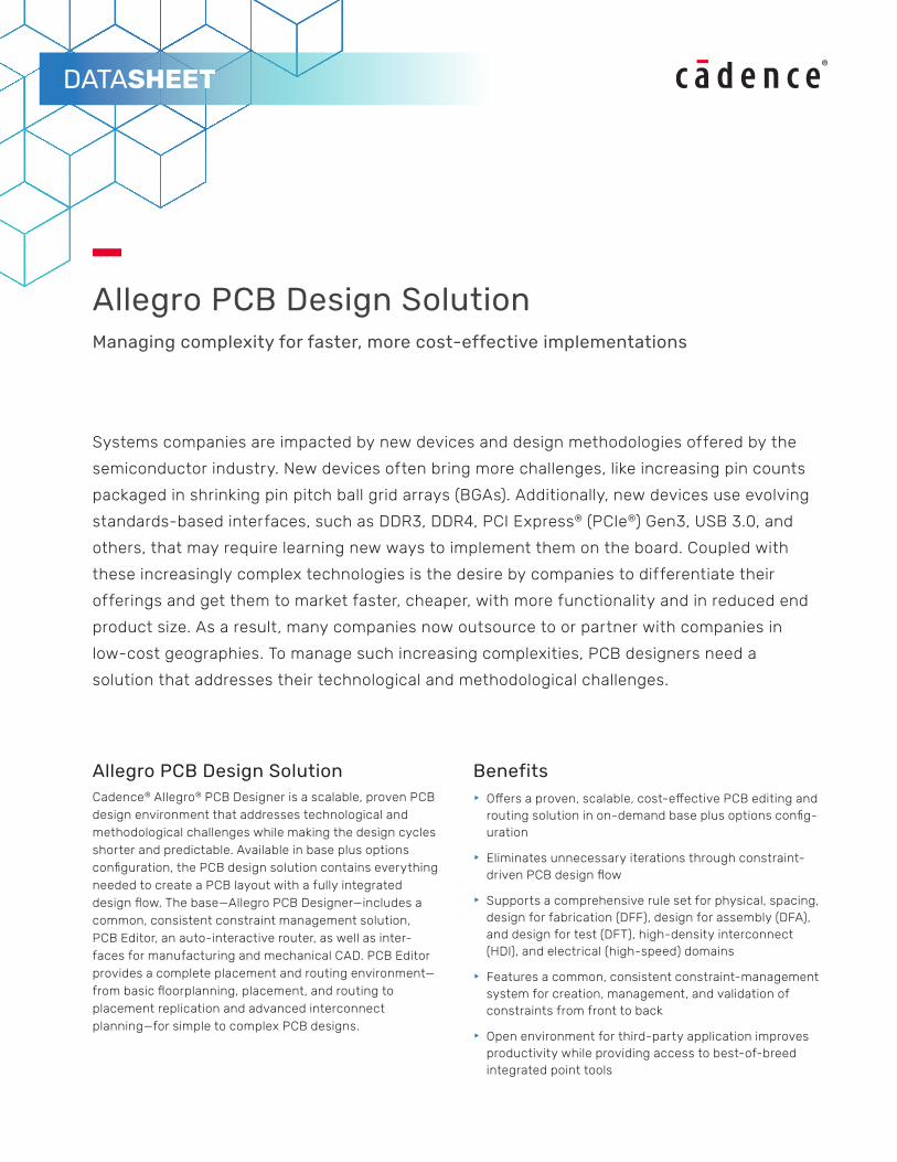
DATASHEET Allegro PCB Design Solution Managing complexity for faster, more cost-effective implementations Systems companies are impacted by new devices and design methodologies offered by the semiconductor industry. New devices often bring more challenges, like increasing pin counts packaged in shrinking pin pitch ball grid arrays (BGAs). Additionally, new devices use evolving standards-based interfaces, such as DDR3, DDR4, PCI Express ® (PCIe ® ) Gen3, USB 3.0, and others, that may require learning new ways to implement them on the board. Coupled with these increasingly complex technologies is the desire by companies to differentiate their offerings and get them to market faster, cheaper, with more functionality and in reduced end product size. As a result, many companies now outsource to or partner with companies in low-cost geographies. To manage such increasing complexities, PCB designers need a solution that addresses their technological and methodological challenges. Allegro PCB Design Solution Cadence ® Allegro ® PCB Designer is a scalable, proven PCB design environment that addresses technological and methodological challenges while making the design cycles shorter and predictable. Available in base plus options configuration, the PCB design solution contains everything needed to create a PCB layout with a fully integrated design flow. The base—Allegro PCB Designer—includes a common, consistent constraint management solution, PCB Editor, an auto-interactive router, as well as inter- faces for manufacturing and mechanical CAD. PCB Editor provides a complete placement and routing environment— from basic floorplanning, placement, and routing to placement replication and advanced interconnect planning—for simple to complex PCB designs. Benefits f Offers a proven, scalable, cost-effective PCB editing and routing solution in on-demand base plus options config- uration f Eliminates unnecessary iterations through constraint- driven PCB design flow f Supports a comprehensive rule set for physical, spacing, design for fabrication (DFF), design for assembly (DFA), and design for test (DFT), high-density interconnect (HDI), and electrical (high-speed) domains f Features a common, consistent constraint-management system for creation, management, and validation of constraints from front to back f Open environment for third-party application improves productivity while providing access to best-of-breed integrated point tools
Transcript of Allegro PCB Design Solution - storage.googleapis.com
DATASHEET
Allegro PCB Design SolutionManaging complexity for faster, more cost-effective implementations
Systems companies are impacted by new devices and design methodologies offered by the
semiconductor industry. New devices often bring more challenges, like increasing pin counts
packaged in shrinking pin pitch ball grid arrays (BGAs). Additionally, new devices use evolving
standards-based interfaces, such as DDR3, DDR4, PCI Express® (PCIe®) Gen3, USB 3.0, and
others, that may require learning new ways to implement them on the board. Coupled with
these increasingly complex technologies is the desire by companies to differentiate their
offerings and get them to market faster, cheaper, with more functionality and in reduced end
product size. As a result, many companies now outsource to or partner with companies in
low-cost geographies. To manage such increasing complexities, PCB designers need a
solution that addresses their technological and methodological challenges.
Allegro PCB Design SolutionCadence® Allegro® PCB Designer is a scalable, proven PCB design environment that addresses technological and methodological challenges while making the design cycles shorter and predictable. Available in base plus options configuration, the PCB design solution contains everything needed to create a PCB layout with a fully integrated design flow. The base—Allegro PCB Designer—includes a common, consistent constraint management solution, PCB Editor, an auto-interactive router, as well as inter-faces for manufacturing and mechanical CAD. PCB Editor provides a complete placement and routing environment—from basic floorplanning, placement, and routing to placement replication and advanced interconnect planning—for simple to complex PCB designs.
Benefitsf Offers a proven, scalable, cost-effective PCB editing and
routing solution in on-demand base plus options config-uration
f Eliminates unnecessary iterations through constraint-driven PCB design flow
f Supports a comprehensive rule set for physical, spacing, design for fabrication (DFF), design for assembly (DFA), and design for test (DFT), high-density interconnect (HDI), and electrical (high-speed) domains
f Features a common, consistent constraint-management system for creation, management, and validation of constraints from front to back
f Open environment for third-party application improves productivity while providing access to best-of-breed integrated point tools
Allegro PCB Design Solution
2www.cadence.com
PCB Editor Technology
Constraint-Driven PCB Editing Environment
At the heart of Allegro PCB Designer is a PCB Editor—an intuitive, easy-to-use, constraint-driven environment for creating and editing simple to complex PCBs. Its extensive feature set addresses a wide range of design and manufac-turability challenges:
f A powerful set of floorplanning and placement tools including placement replication for accelerating placement of the design
f Powerful shape-based shove, hug interactive etch creation, editing establishes a highly productive interconnect environment while providing real-time, heads-up displays of length and timing margins
f Dynamic shape capability offers real-time copper pour plowing and healing functionality during placement and routing iterations
The PCB Editor can also generate a full suite of phototooling, bare-board fabrication, and test outputs, including Gerber 274x, NC drill, and bare-board test in a variety of formats.
Constraint Management
A constraint management system dis- plays physical/spacing and high-speed rules along with their status (based on the current state of the design) in real time and is available at all stages of the design process. Each worksheet provides a spreadsheet interface that enables users to define, manage, and validate the different rules in a hierarchical fashion. With this powerful application, designers can graphically create, edit, and review
constraint sets as graphical topologies that act as electronic blueprints of an ideal implementation strategy. Once they exist in the database, constraints can drive the placement and routing processes for constrained signals.
The constraint management system is completely integrated with the PCB Editor, and constraints can be validated in real time as the design process proceeds. The result of the validation process is a graphical representation of whether constraints pass (highlighted in green) or fail (highlighted in red). This approach allows designers to immediately see the progress of the design in the spread-sheets, as well as the impact of any design changes.
Floorplanning and Placement
The constraint and rules-driven methodology of PCB design solutions includes a powerful and flexible set of placement capabilities, including interactive and automatic. The engineer or designer can assign components or subcir-cuits to specific “rooms” during design entry or floor-planning. Components can be filtered and selected by reference designator, device package/footprint style, associated net name, part number, or the schematic sheet/page number.
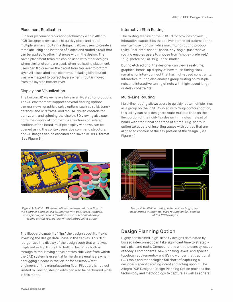
With thousands of components comprising today’s boards, precise management is critical. Real-time assembly analysis and feedback can facilitate this management—helping designers increase productivity and efficiency by placing components according to corporate or EMS guide-lines. Dynamic DFA-driven placement offers real-time package-to-package clearance checking during interactive component placement (see Figure 2). Driven from a two-di-mensional spreadsheet array of classes and package instances, real-time feedback provides minimum clearance requirements. Based on the package’s side-to-side, side-to-end, designers can simultaneously place devices for optimum routability, manufacturability, and signal timing.
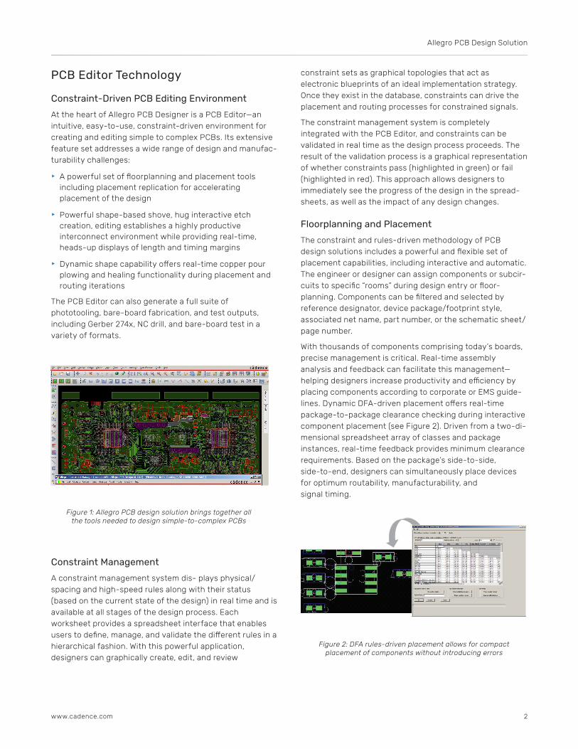
Figure 1: Allegro PCB design solution brings together all the tools needed to design simple-to-complex PCBs
Figure 2: DFA rules-driven placement allows for compact placement of components without introducing errors
Allegro PCB Design Solution
3www.cadence.com
Placement Replication
Superior placement replication technology within Allegro PCB Designer allows users to quickly place and route multiple similar circuits in a design. It allows users to create a template using one instance of placed and routed circuit that can be applied to other instances within the design. The saved placement template can be used with other designs where similar circuits are used. When replicating placement, users can flip or mirror the circuit from top layer to bottom layer. All associated etch elements, including blind buried vias, are mapped to correct layers when circuit is moved from top layer to bottom layer.
Display and Visualization
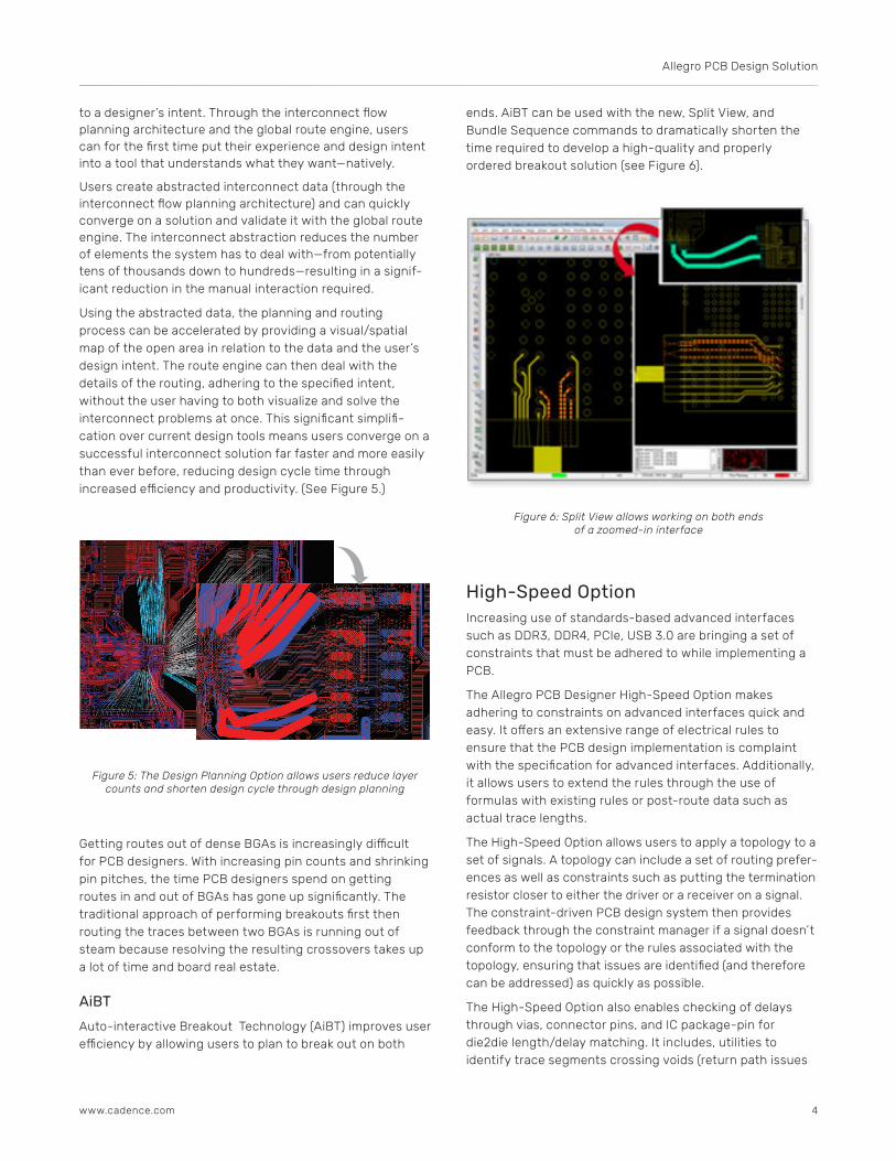
The built-in 3D viewer is available in all PCB Editor products. The 3D environment supports several filtering options, camera views, graphic display options such as solid, trans-parency, and wireframe, and mouse-driven controls for pan, zoom, and spinning the display. 3D viewing also sup- ports the display of complex via structures or isolated sections of the board. Multiple display windows can be opened using the context sensitive command structure, and 3D images can be captured and saved in JPEG format. (See Figure 3.)
The flipboard capability “flips” the design about its Y axis inverting the design data- base in the canvas. This “flip” reorganizes the display of the design such that what was displayed as top through to bottom becomes bottom through to top. Having a true bottom side view from within the CAD system is essential for hardware engineers when debugging a board in the lab, or for assembly/test engineers on the manufacturing floor. Flipboard is not just limited to viewing; design edits can also be performed while in this mode.
Interactive Etch Editing
The routing feature of the PCB Editor provides powerful, interactive capabilities that deliver controlled automation to maintain user control, while maximizing routing produc-tivity. Real-time, shape- based, any-angle, push/shove routing enables users to choose from “shove- preferred,” “hug-preferred,” or “hug- only” modes.
During etch editing, the designer can view a real-time, graphical heads-up display of how much timing slack remains for inter- connect that has high-speed constraints. Interactive routing also enables group routing on multiple nets and interactive tuning of nets with high-speed length or delay constraints.
Multi-Line Routing
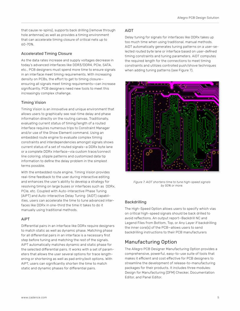
Multi-line routing allows users to quickly route multiple lines as a group on the PCB. Coupled with “hug-contour” option, this utility can help designers route multiple lines on the flex portion of the rigid-flex design in minutes instead of hours with traditional one trace at a time. Hug-contour option takes care of inserting traces with curves that are aligned to contour of the flex portion of the design. (See Figure 4.)
Design Planning OptionHighly constrained, high-density designs dominated by bussed interconnect can take significant time to strategi-cally plan and route. Compound this with the density issues of today’s components, new signaling levels, and specific topology requirements—and it’s no wonder that traditional CAD tools and technologies fall short of capturing a designer’s specific routing intent and acting upon it. The Allegro PCB Designer Design Planning Option provides the technology and methodology to capture as well as adhere
Figure 3: Built-in 3D viewer allows reviewing of a section of the board or complex via structures with pan, zoom, rotation,
and spinning to reduce iterations with mechanical design teams or PCB fabricators without introducing errors
Figure 4: Multi-line routing with contour hug option accelerates through no-click routing on flex section
of the PCB designs
Allegro PCB Design Solution
4www.cadence.com
to a designer’s intent. Through the interconnect flow planning architecture and the global route engine, users can for the first time put their experience and design intent into a tool that understands what they want—natively.
Users create abstracted interconnect data (through the interconnect flow planning architecture) and can quickly converge on a solution and validate it with the global route engine. The interconnect abstraction reduces the number of elements the system has to deal with—from potentially tens of thousands down to hundreds—resulting in a signif-icant reduction in the manual interaction required.
Using the abstracted data, the planning and routing process can be accelerated by providing a visual/spatial map of the open area in relation to the data and the user’s design intent. The route engine can then deal with the details of the routing, adhering to the specified intent, without the user having to both visualize and solve the interconnect problems at once. This significant simplifi-cation over current design tools means users converge on a successful interconnect solution far faster and more easily than ever before, reducing design cycle time through increased efficiency and productivity. (See Figure 5.)
Getting routes out of dense BGAs is increasingly difficult for PCB designers. With increasing pin counts and shrinking pin pitches, the time PCB designers spend on getting routes in and out of BGAs has gone up significantly. The traditional approach of performing breakouts first then routing the traces between two BGAs is running out of steam because resolving the resulting crossovers takes up a lot of time and board real estate.
AiBT
Auto-interactive Breakout Technology (AiBT) improves user efficiency by allowing users to plan to break out on both
ends. AiBT can be used with the new, Split View, and Bundle Sequence commands to dramatically shorten the time required to develop a high-quality and properly ordered breakout solution (see Figure 6).
High-Speed OptionIncreasing use of standards-based advanced interfaces such as DDR3, DDR4, PCIe, USB 3.0 are bringing a set of constraints that must be adhered to while implementing a PCB.
The Allegro PCB Designer High-Speed Option makes adhering to constraints on advanced interfaces quick and easy. It offers an extensive range of electrical rules to ensure that the PCB design implementation is complaint with the specification for advanced interfaces. Additionally, it allows users to extend the rules through the use of formulas with existing rules or post-route data such as actual trace lengths.
The High-Speed Option allows users to apply a topology to a set of signals. A topology can include a set of routing prefer-ences as well as constraints such as putting the termination resistor closer to either the driver or a receiver on a signal. The constraint-driven PCB design system then provides feedback through the constraint manager if a signal doesn’t conform to the topology or the rules associated with the topology, ensuring that issues are identified (and therefore can be addressed) as quickly as possible.
The High-Speed Option also enables checking of delays through vias, connector pins, and IC package-pin for die2die length/delay matching. It includes, utilities to identify trace segments crossing voids (return path issues
Figure 5: The Design Planning Option allows users reduce layer counts and shorten design cycle through design planning
Figure 6: Split View allows working on both ends of a zoomed-in interface
Allegro PCB Design Solution
5www.cadence.com
that cause re-spins), supports back drilling (remove through hole antennas) as well as provides a timing environment that can accelerate timing closure of critical nets up to 60-70%.
Accelerated Timing Closure
As the data rates increase and supply voltages decrease in today’s advanced interfaces like DDR3/DDR4, PCIe, SATA, etc., PCB designers must spend more time to ensure signals in an interface meet timing requirements. With increasing density on PCBs, the effort to get to timing closure—ensuring all signals meet timing requirements—can increase significantly. PCB designers need new tools to meet this increasingly complex challenge.
Timing Vision
Timing Vision is an innovative and unique environment that allows users to graphically see real-time delay and phase information directly on the routing canvas. Traditionally, evaluating current status of timing/length of a routed interface requires numerous trips to Constraint Manager and/or use of the Show Element command. Using an embedded route engine to evaluate complex timing constraints and interdependencies amongst signals shows current status of a set of routed signals—a DDRx byte lane or a complete DDRx interface—via custom trace/connect line coloring; stipple patterns and customized data tip information to define the delay problem in the simplest terms possible.
With the embedded route engine, Timing Vision provides real-time feedback to the user during interactive editing and enhances the user’s ability to develop a strategy for resolving timing on large buses or interfaces such as DDRx, PCIe, etc. Coupled with Auto-interactive Phase Tuning (AiPT) and Auto-interactive Delay Tuning (AiDT) capabil-ities, users can accelerate the time to tune advanced inter-faces like DDRx in one-third the time it takes to do it manually using traditional methods.
AiPT
Differential pairs in an interface like DDRx require designers to match static as well as dynamic phase. Matching phase for all differential pairs in an interface is a necessary first step before tuning and matching the rest of the signals. AiPT automatically matches dynamic and static phase for the selected differential pairs. It works with a set of param-eters that allows the user several options for trace length-ening or shortening as well as pad entry/exit options. With AiPT, users can significantly shorten the time to match static and dynamic phases for differential pairs.
AiDT
Delay tuning for signals for interfaces like DDRx takes up too much time when using traditional, manual methods. AiDT automatically generates tuning patterns on a user-se-lected routed byte lane or interface based on user-defined timing constraints and tuning parameters. AiDT computes the required length for the connections to meet timing constraints and utilizes controlled push/shove techniques when adding tuning patterns (see Figure 7).
Backdrilling
The High-Speed Option allows users to specify which vias on critical high-speed signals should be back drilled to avoid reflections. An output report—Backdrill NC and Legend Files from Bottom, Top, or Any Layer if backdrilling the inner core(s) of the PCB—allows users to send backdrilling instructions to their PCB manufacturers
Manufacturing OptionThe Allegro PCB Designer Manufacturing Option provides a comprehensive, powerful, easy-to-use suite of tools that makes it efficient and cost effective for PCB designers to streamline the development of release-to-manufacturing packages for their products. It includes three modules: Design for Manufacturing (DFM) Checker, Documentation Editor, and Panel Editor.
Figure 7: AiDT shortens time to tune high-speed signals by 50% or more.
Allegro PCB Design Solution
6www.cadence.com
DFM Checker
The Manufacturing Option’s DFM Checker module is designed for engineers and designers who appreciate the benefits of manufacturing analysis and want to conduct it in a robust environment, with ease and sensibility at any phase of the PCB design process. DFM Checker offers comprehensive analysis for all major PCB design tools, Gerber files, intelligent manufacturing files, and NC data to ensure the content supplied to the manufacturer will minimize costly delays.
Documentation Editor
The Manufacturing Option’s Documentation Editor is a PCB documentation-authoring tool that intelligently automates your documentation creation process to produce complex PCB documentation in a fraction of the time versus tradi-tional methods. Documentation Editor enables you to quickly create the manufacturing drawings that drive PCB fabrication and assembly.
Panel Editor
The Manufacturing Option’s Panel Editor module intelli-gently automates the complex process of panel definition and documentation, simplifying the design process. This solution enables designers to quickly create electronic manufacturing documents that clearly articulate the panel specification and instructions for successful fabrication, assembly, and inspection of their designs.
Design Data Transfer to Manufacturing
A full suite of phototooling, bare-board fabrication, and test outputs, including Gerber 274x, NC drill, and bare-board test in a variety of formats, can be generated. More importantly, Cadence supports the industry initiative toward Gerber-less manufacturing through export and import of design data in IPC-2581 format. The IPC-2581 data is passed in a single file that creates accurate and reliable manufacturing data for high-quality manufacturing. Users have a choice to export a subset of the design data for protecting their IP. Import of IPC-2581 is intended for overlaying artwork data on the design for viewing purposes only.
Miniaturization Option
Constraint-Driven HDI Design Flow
With BGA pin pitches decreasing to below 1mm, (0.8mm or lower with 0.65mm or 0.5mm pin pitches), users are forced to implement a buildup PCB technology using HDI.
While miniaturization is not necessarily the primary objective in many market segments, the move to buildup
technology is necessary for fanning out a BGA— particularly if it has three or four rows of pins on each side.
The Allegro PCB Designer Miniaturization Option offers a proven constraint-driven HDI design flow with a compre-hensive set of design rules for all different styles of HDI designs, from a hybrid buildup/core combination to a complete buildup process like ALIVH.
In addition, it includes automation for adding HDI to shorten the time to create designs that are correct by construction.
Embedded Components
Reducing end product size can be accomplished in many different ways. One of the approaches PCB designers are taking is to embed packaged components on inner layers. The Miniaturization Option offers constraint-driven embedded component placement and routing. It supports direct- and indirect-attach techniques, and supports embedding components with dual-sided contacts, vertical components, and embedding in dielectric on a two-layer PCB. Additionally it offers the ability to create and manage cavities on layers specified for embedding components.
Analog/RF OptionThe Allegro PCB Designer Analog/RF Option offers a mixed-signal design environment, from schematic to layout with back annotation, proven to increase RF design productivity up to 50%. It allows engineers to create, integrate, and update analog/RF/microwave circuits with digital/analog circuits in the Allegro PCB Design environment. With its rich layout capability and powerful interfaces with RF simulation tools, it allows engineers to start RF design from Allegro Design Authoring, Allegro PCB Designer, or Keysight Technologies Advanced Design System (ADS).
Team Design OptionGlobally dispersed design teams are on the rise, which compounds the challenge of shortening design cycle times. Manual workarounds that address multi-user issues are time-consuming, slow, and prone to error.
The Allegro PCB Designer Team Design Option provides a multi-user, concurrent design methodology for faster time to market and reduced layout time. Multiple designers working concurrently on a layout share access to a single database, regardless of team proximity. Designers can partition designs into multiple sections or areas for layout and editing by several design team members. Designs can be partitioned vertically (sections) with soft boundaries or horizontally (layers). As a result, each designer can see all partitioned sections and update the design view for monitoring the status and progress of other users’ sections. Such partitioning can dramatically reduce overall design cycles and accelerate the design process.
Allegro PCB Design Solution
7www.cadence.com
Routing OptionThe Allegro PCB Designer Routing Option is tightly integrated with the PCB Editor. Through the Routing Option interface, all design information and constraints are automatically passed from the PCB Editor. Once the route is completed, all route information is automatically passed back to the PCB Editor.
Increased design complexity, density, and high-speed routing constraints make manual routing of PCBs difficult and time-consuming. The challenges inherent in complex interconnect routing are best addressed with powerful, automated technology. The robust, production-proven autorouter includes a batch routing mode with extensive user-defined routing strategy control as well as built-in automatic strategy capabilities.
DFM Rules-Driven Autorouting
The design for manufacturing capability within the Routing Option significantly improves manufacturing yields. Manufacturing algorithms provide a spreading capability that automatically increases conductor clearances on a space-available basis. Automatic conductor spreading helps improve manufactuability by repositioning conductors to create extra space between conductors and pins, conductors and SMD pads, and adjacent conductor segments. Users gain the flexibility to define a range of spacing values or to use the default values.
Mitered corners and test points can be added throughout the routing process. The manufacturing algorithms automatically use the optimal setback range, starting from the largest to the smallest value. Test point insertion automatically adds testable vias or pads as test points. Testable vias can be probed on the front, back, or both sides of the PCB, supporting both single side and clamshell testers. Designers have the flexibility to select the test point insertion methodology that conforms to their manufacturing requirements. Test points can be “fixed” to avoid costly test fixture modifications. Test point constraints include test probe surfaces, via sizes, via grids, and minimum center-to- center distance.
High-Speed Constraints-Driven Autorouting
High-speed routing constraints and algorithms handle differential pairs, net scheduling, timing, crosstalk, layer set routing, and the special geometry requirements demanded by today’s high-speed circuits. The autorouting algorithms
intelligently handle routing around or through vias, and automatically conform to defined length or timing criteria. Automatic net shielding is used to reduce noise on noise- sensitive nets. Separate design rules may be applied to different regions of the design; for example, you can specify tight clearance rules in the connector area of a design and less stringent rules elsewhere.
Operating System SupportAllegro Platform Technology:
f Sun Solaris
f Linux
f IBM AIX
f Windows
OrCAD Technology:
f Windows
Cadence Services and Supportf Cadence application engineers can answer your technical
questions by telephone, email, or Internet—they can also provide technical assistance and custom training
f Cadence certified instructors teach more than 70 courses and bring their real-world experience into the classroom
f More than 25 Internet Learning Series (iLS) online courses allow you the flexibility of training at your own computer via the Internet
f Cadence Online Support gives you 24x7 online access to a knowledge base of the latest solutions, technical documentation, software downloads, and more
For More InformationFor product sales, support, or additional information on Allegro solutions, visit www.cadence.com/contact_us to locate a Cadence Sales office or channel partner in your area.
Allegro PCB Design Solution
8www.cadence.com
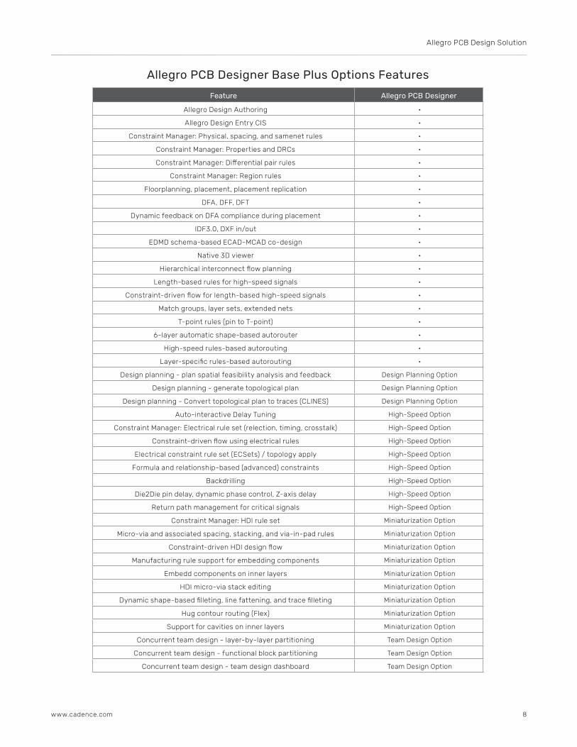
Allegro PCB Designer Base Plus Options Features
Feature Allegro PCB Designer
Allegro Design Authoring •
Allegro Design Entry CIS •
Constraint Manager: Physical, spacing, and samenet rules •
Constraint Manager: Properties and DRCs •
Constraint Manager: Differential pair rules •
Constraint Manager: Region rules •
Floorplanning, placement, placement replication •
DFA, DFF, DFT •
Dynamic feedback on DFA compliance during placement •
IDF3.0, DXF in/out •
EDMD schema-based ECAD-MCAD co-design •
Native 3D viewer •
Hierarchical interconnect flow planning •
Length-based rules for high-speed signals •
Constraint-driven flow for length-based high-speed signals •
Match groups, layer sets, extended nets •
T-point rules (pin to T-point) •
6-layer automatic shape-based autorouter •
High-speed rules-based autorouting •
Layer-specific rules-based autorouting •
Design planning - plan spatial feasibility analysis and feedback Design Planning Option
Design planning - generate topological plan Design Planning Option
Design planning - Convert topological plan to traces (CLINES) Design Planning Option
Auto-interactive Delay Tuning High-Speed Option
Constraint Manager: Electrical rule set (relection, timing, crosstalk) High-Speed Option
Constraint-driven flow using electrical rules High-Speed Option
Electrical constraint rule set (ECSets) / topology apply High-Speed Option
Formula and relationship-based (advanced) constraints High-Speed Option
Backdrilling High-Speed Option
Die2Die pin delay, dynamic phase control, Z-axis delay High-Speed Option
Return path management for critical signals High-Speed Option
Constraint Manager: HDI rule set Miniaturization Option
Micro-via and associated spacing, stacking, and via-in-pad rules Miniaturization Option
Constraint-driven HDI design flow Miniaturization Option
Manufacturing rule support for embedding components Miniaturization Option
Embedd components on inner layers Miniaturization Option
HDI micro-via stack editing Miniaturization Option
Dynamic shape-based filleting, line fattening, and trace filleting Miniaturization Option
Hug contour routing (Flex) Miniaturization Option
Support for cavities on inner layers Miniaturization Option
Concurrent team design - layer-by-layer partitioning Team Design Option
Concurrent team design - functional block partitioning Team Design Option
Concurrent team design - team design dashboard Team Design Option
Cadence is a pivotal leader in electronic design and computational expertise, using its Intelligent System Design strategy to turn design concepts into reality. Cadence customers are the world’s most creative and innovative companies, delivering extraordinary electronic products from chips to boards to systems for the most dynamic market applications. www.cadence.com
© 2021 Cadence Design Systems, Inc. All rights reserved worldwide. Cadence, the Cadence logo, and the other Cadence marks found at www. cadence.com/go/trademarks are trademarks or registered trademarks of Cadence Design Systems, Inc. All other trademarks are the property of their respective owners. 16097 04/21 SA/VY/PDF
Allegro PCB Design Solution
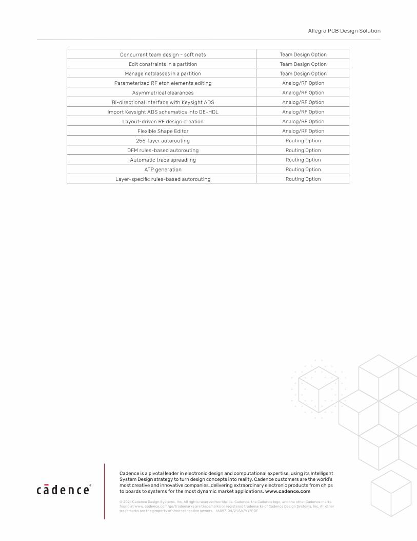
Concurrent team design - soft nets Team Design Option
Edit constraints in a partition Team Design Option
Manage netclasses in a partition Team Design Option
Parameterized RF etch elements editing Analog/RF Option
Asymmetrical clearances Analog/RF Option
Bi-directional interface with Keysight ADS Analog/RF Option
Import Keysight ADS schematics into DE-HDL Analog/RF Option
Layout-driven RF design creation Analog/RF Option
Flexible Shape Editor Analog/RF Option
256-layer autorouting Routing Option
DFM rules-based autorouting Routing Option
Automatic trace spreadiing Routing Option
ATP generation Routing Option
Layer-specific rules-based autorouting Routing Option