
All-optical transistor action with bistable switching in a ...soljacic/ao_transistor_OL.pdf · We...
3
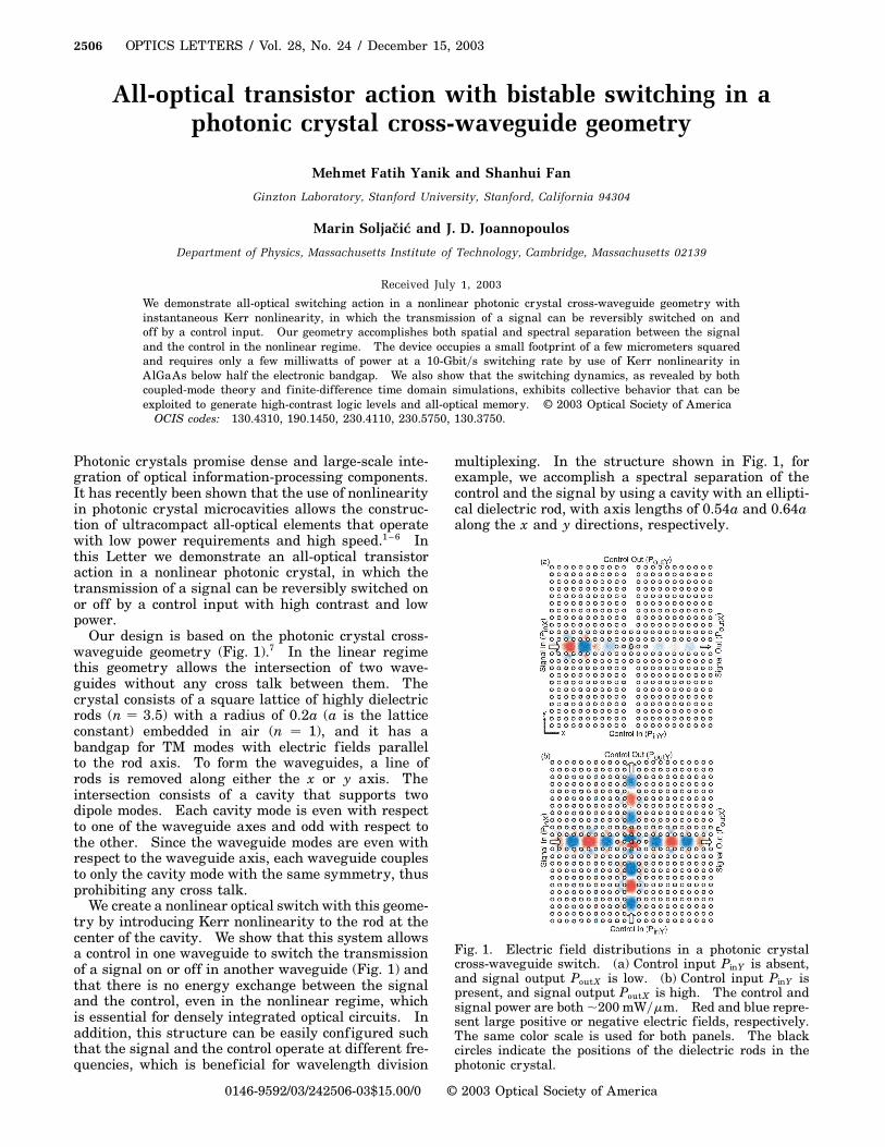
2506 OPTICS LETTERS / Vol. 28, No. 24 / December 15, 2003 All-optical transistor action with bistable switching in a photonic crystal cross-waveguide geometry Mehmet Fatih Yanik and Shanhui Fan Ginzton Laboratory, Stanford University, Stanford, California 94304 Marin Soljaˇ cic ´ and J. D. Joannopoulos Department of Physics, Massachusetts Institute of Technology, Cambridge, Massachusetts 02139 Received July 1, 2003 We demonstrate all-optical switching action in a nonlinear photonic crystal cross-waveguide geometry with instantaneous Kerr nonlinearity, in which the transmission of a signal can be reversibly switched on and off by a control input. Our geometry accomplishes both spatial and spectral separation between the signal and the control in the nonlinear regime. The device occupies a small footprint of a few micrometers squared and requires only a few milliwatts of power at a 10-Gbits switching rate by use of Kerr nonlinearity in AlGaAs below half the electronic bandgap. We also show that the switching dynamics, as revealed by both coupled-mode theory and finite-difference time domain simulations, exhibits collective behavior that can be exploited to generate high-contrast logic levels and all-optical memory. © 2003 Optical Society of America OCIS codes: 130.4310, 190.1450, 230.4110, 230.5750, 130.3750. Photonic crystals promise dense and large-scale inte- gration of optical information-processing components. It has recently been shown that the use of nonlinearity in photonic crystal microcavities allows the construc- tion of ultracompact all-optical elements that operate with low power requirements and high speed. 1–6 In this Letter we demonstrate an all-optical transistor action in a nonlinear photonic crystal, in which the transmission of a signal can be reversibly switched on or off by a control input with high contrast and low power. Our design is based on the photonic crystal cross- waveguide geometry (Fig. 1). 7 In the linear regime this geometry allows the intersection of two wave- guides without any cross talk between them. The crystal consists of a square lattice of highly dielectric rods (n 3.5) with a radius of 0.2a (a is the lattice constant) embedded in air (n 1), and it has a bandgap for TM modes with electric fields parallel to the rod axis. To form the waveguides, a line of rods is removed along either the x or y axis. The intersection consists of a cavity that supports two dipole modes. Each cavity mode is even with respect to one of the waveguide axes and odd with respect to the other. Since the waveguide modes are even with respect to the waveguide axis, each waveguide couples to only the cavity mode with the same symmetry, thus prohibiting any cross talk. We create a nonlinear optical switch with this geome- try by introducing Kerr nonlinearity to the rod at the center of the cavity. We show that this system allows a control in one waveguide to switch the transmission of a signal on or off in another waveguide (Fig. 1) and that there is no energy exchange between the signal and the control, even in the nonlinear regime, which is essential for densely integrated optical circuits. In addition, this structure can be easily configured such that the signal and the control operate at different fre- quencies, which is beneficial for wavelength division multiplexing. In the structure shown in Fig. 1, for example, we accomplish a spectral separation of the control and the signal by using a cavity with an ellipti- cal dielectric rod, with axis lengths of 0.54a and 0.64a along the x and y directions, respectively. Fig. 1. Electric field distributions in a photonic crystal cross-waveguide switch. (a) Control input P inY is absent, and signal output P outX is low. (b) Control input P inY is present, and signal output P outX is high. The control and signal power are both 200 mWmm. Red and blue repre- sent large positive or negative electric fields, respectively. The same color scale is used for both panels. The black circles indicate the positions of the dielectric rods in the photonic crystal. 0146-9592/03/242506-03$15.00/0 © 2003 Optical Society of America
Transcript of All-optical transistor action with bistable switching in a ...soljacic/ao_transistor_OL.pdf · We...
2506 OPTICS LETTERS / Vol. 28, No. 24 / December 15, 2003
All-optical transistor action with bistable switching in aphotonic crystal cross-waveguide geometry
Mehmet Fatih Yanik and Shanhui Fan
Ginzton Laboratory, Stanford University, Stanford, California 94304
Marin Soljacic and J. D. Joannopoulos
Department of Physics, Massachusetts Institute of Technology, Cambridge, Massachusetts 02139
Received July 1, 2003
We demonstrate all-optical switching action in a nonlinear photonic crystal cross-waveguide geometry withinstantaneous Kerr nonlinearity, in which the transmission of a signal can be reversibly switched on andoff by a control input. Our geometry accomplishes both spatial and spectral separation between the signaland the control in the nonlinear regime. The device occupies a small footprint of a few micrometers squaredand requires only a few milliwatts of power at a 10-Gbit�s switching rate by use of Kerr nonlinearity inAlGaAs below half the electronic bandgap. We also show that the switching dynamics, as revealed by bothcoupled-mode theory and finite-difference time domain simulations, exhibits collective behavior that can beexploited to generate high-contrast logic levels and all-optical memory. © 2003 Optical Society of America
OCIS codes: 130.4310, 190.1450, 230.4110, 230.5750, 130.3750.
Photonic crystals promise dense and large-scale inte-gration of optical information-processing components.It has recently been shown that the use of nonlinearityin photonic crystal microcavities allows the construc-tion of ultracompact all-optical elements that operatewith low power requirements and high speed.1 – 6 Inthis Letter we demonstrate an all-optical transistoraction in a nonlinear photonic crystal, in which thetransmission of a signal can be reversibly switched onor off by a control input with high contrast and lowpower.
Our design is based on the photonic crystal cross-waveguide geometry (Fig. 1).7 In the linear regimethis geometry allows the intersection of two wave-guides without any cross talk between them. Thecrystal consists of a square lattice of highly dielectricrods (n � 3.5) with a radius of 0.2a (a is the latticeconstant) embedded in air (n � 1), and it has abandgap for TM modes with electric f ields parallelto the rod axis. To form the waveguides, a line ofrods is removed along either the x or y axis. Theintersection consists of a cavity that supports twodipole modes. Each cavity mode is even with respectto one of the waveguide axes and odd with respect tothe other. Since the waveguide modes are even withrespect to the waveguide axis, each waveguide couplesto only the cavity mode with the same symmetry, thusprohibiting any cross talk.
We create a nonlinear optical switch with this geome-try by introducing Kerr nonlinearity to the rod at thecenter of the cavity. We show that this system allowsa control in one waveguide to switch the transmissionof a signal on or off in another waveguide (Fig. 1) andthat there is no energy exchange between the signaland the control, even in the nonlinear regime, whichis essential for densely integrated optical circuits. Inaddition, this structure can be easily conf igured suchthat the signal and the control operate at different fre-quencies, which is beneficial for wavelength division
0146-9592/03/242506-03$15.00/0
multiplexing. In the structure shown in Fig. 1, forexample, we accomplish a spectral separation of thecontrol and the signal by using a cavity with an ellipti-cal dielectric rod, with axis lengths of 0.54a and 0.64aalong the x and y directions, respectively.
Fig. 1. Electric field distributions in a photonic crystalcross-waveguide switch. (a) Control input PinY is absent,and signal output PoutX is low. (b) Control input PinY ispresent, and signal output PoutX is high. The control andsignal power are both �200 mW�mm. Red and blue repre-sent large positive or negative electric fields, respectively.The same color scale is used for both panels. The blackcircles indicate the positions of the dielectric rods in thephotonic crystal.
© 2003 Optical Society of America

December 15, 2003 / Vol. 28, No. 24 / OPTICS LETTERS 2507
The dynamic behavior of the system can be describedwith the following coupled-mode equations:
dSoutX
dt� ivXSoutX 2 igX
µjSoutX j
2
PXX1 2
jSoutY j2
PXY
∂SoutX
1 gX �SinX 2 SoutX� 2 igXSoutY
2
PXYSoutX
�,
(1)
dSoutY
dt� ivYSoutY 2 igY
µjSoutY j
2
PYY1 2
jSoutX j2
PYX
∂SoutY
1 gY �SinY 2 SoutY � 2 igYSoutX
2
PYXSoutY
�.
(2)
Sin�out�j is proportional to the field amplitude suchthat Pin�out�j � jSin�out�j j
2 is the input (output) powerin waveguide j . The subscripts X and Y labeleither the waveguide that is parallel to the x or yaxis, respectively, or the cavity mode that couplesto the waveguide. gj � vj�2Qj is the decay ratefor cavity mode j . Pij � �2aij �vi�c�d21n2QiQj�21
are the characteristic powers of the system with
aij �
µc
vi
∂dRvol d
dr�jEi�r� ? Ej �r�j2 1 2jEi�r� ? Ej��r�j2�n2�r�n2�r�
�Rvol ddrjEi�r�j2n2�r�� �
Rvol ddrjEj �r�j2n2�r��n2�r�max
, (3)
where a is the generalization of the dimensionlessscale-invariant nonlinear feedback parameter definedin Ref. 3; here aii and aij are the self- and cross-modaloverlap factors for the two cavity modes i and j andare obtained from the first-order perturbation theoryin terms of the electric fields in the cavity modesEi�j ��r� � 1/2 �Ei� j ��r�exp�ivt� 1 Ei� j �
��r�exp�2ivt��.n2, vj , a, and c are the instantaneous Kerr nonlin-earity coefficient, the angular frequency of cavitymode j , the lattice constant of the photonic crystal,and the speed of light, respectively. The last termson the right-hand side of Eqs. (1) and (2) describea nonlinear energy exchange process between thecontrol and the signal, which become negligible whenthe frequencies of the signal and control inputs andthe corresponding resonances of the cavity modes areseparated by more than the width of the resonances,as in our simulations.
With Eqs. (1) and (2) the general switching behaviorof the system can be understood qualitatively asfollows: In the absence of the control beam (i.e.,SinY � 0) the signal output versus the signal inputexhibits the typical bistable shape in a transmissionresonator configuration,8 as shown with the blue solidcurve in Fig. 2. Suppose the signal output level isoriginally at point A in Fig. 2. Applying a controlbeam (i.e., nonzero SinY and SoutY ) shifts the frequencyof mode X by an amount that is proportional to jSoutY j
2.The bistable transition threshold of the signal is thusdecreased (e.g., the red curve, Fig. 2), resulting in anabrupt transition in the signal output power. There-fore at a given signal input power the control can
stimulate transitions between the bistable states andgenerate high-contrast logic levels. When the controlis turned off, the bistability curve for the signal outputmoves back to the blue curve, and the signal outputdrops to the original level at point A. Such reversibleswitching occurs when the signal input power levellies below the bistable threshold in the absence ofthe control. For a higher signal input power (forexample, point C in Fig. 2) the signal output remainsat a higher power level (point E) after the control isturned off, thus exhibiting memory behavior.
Since the transmission of the control is also beingmodulated by the signal, the detailed switching dy-namics is more complicated than in the qualitativediscussions presented above. Below we present arigorous analysis by combining finite-difference timedomain (FDTD) simulations with coupled-mode theory.We show that the mutual coupling between the signaland the control can lead to significant improvementsin the switching contrast.
We employ the same nonlinear FDTD simula-tions9 as in Ref. 5. We choose a Kerr coefficient ofn2 � 1.5 3 10217 W�m2, which is achievable withnearly instantaneous nonlinearity in AlGaAs belowhalf the electronic bandgap10,11 at 1.55 mm. At a
low incident power at which the structure behaveslinearly we determine that the cavity modes haveresonance frequencies of vX � 0.373�2pc�a� andvY � 0.355�2pc�a�, which fall within the bandgapof the photonic crystal; quality factors of QX � 920and QY � 1005; and nonlinear modal overlap fac-tors of aXX � 0.154, aYY � 0.172, aXY � 0.051,and aYX � 0.056. With these parameters and alattice constant of a � 575 nm the theory predictscharacteristic powers of PXX � 62.75 mW�mm,PYY � 49.26 mW�mm, PXY � 172.55 mW�mm, andPYX � 164.32 mW�mm.
Fig. 2. Input versus output power for the signal in wave-guide X, calculated with Eq. (1), with the output powerin waveguide Y (and hence the energy in cavity mode Y)kept at constant levels. Blue, red, and green curves corre-spond to control output powers of 0, 151, and 75 mW�mm,respectively, which is appropriate for various times in theswitching process, as shown in Fig. 3.

2508 OPTICS LETTERS / Vol. 28, No. 24 / December 15, 2003
Fig. 3. Input and output power levels for the signal andthe control as a function of time. The curves are fromcoupled-mode theory calculations with Eqs. (1) and (2), andthe open circles and triangles are from FDTD simulations.The labels A, B, and B0 indicate the control output powerlevels that were used to calculate the bistability curves inFig. 2.
To demonstrate the transistor action, we launch asignal in waveguide X with carrier frequency vinXdetuned by dX � �vX 2 vinX��gX � 2
p3 from the
resonance of cavity mode X, as shown with the solidblue curve in Fig. 3. (d �
p3 is the minimum de-
tuning threshold for the presence of bistability in theabsence of control input.) The power of the inputPinX � 200 mW�mm is selected to be below the bistableregion in the absence of the control input (point A onthe blue curve in Fig. 2). The field pattern of thesteady state at t � 15 ps is shown in Fig. 1(a). Afterthe steady state has been reached, we launch a controlpulse with detuning dY � �vY 2 vinY ��gY � 1.4
p3
and a power of PinY � 205 mW�mm in waveguide Y ,as shown with the green solid curve in Fig. 3. Thecontrol switches the signal output to a higher level inapproximately 10 ps (point B on the green bistabilitycurve in Fig. 2). The field pattern of the steady statein the presence of the control is shown in Fig. 1(b).Finally, we turn off the control at t � 45 ps, and thesignal output returns to a low transmission state,completing a reversible switching cycle. There isexcellent agreement between our FDTD results andcoupled-mode theory with Eqs. (1) and (2).5
An interesting feature in Fig. 3 is the presence of apeak in the control output during the initial transientperiod (labeled as B0). As the control input is switchedon, the power in mode Y initially increases, which in-duces the transition in signal output from point A topoint B0 by moving the bistability curve for the signalfrom the blue curve to the red curve in Fig. 2. In themeantime, however, as the energy increases in the cav-ity modes, the frequency of mode Y also starts to shiftdownward, detuning from the control input; eventuallyreduces its energy from its peak value; and moves thebistability curve for the signal from the red curve to thegreen curve in Fig. 2. Such collective dynamics canthus be used to generate high contrast in signal output(point B in Fig. 3) with a low power threshold. To ex-
ploit this effect, we have chosen a finite detuning dY �1.4
p3 of the control input from cavity resonance Y .
We note from Eqs. (1) and (2) that the nonlinearitydoes not mix the signal and control outputs when theirfrequencies are separated by more than the cavity reso-nance widths. This is confirmed in the FDTD simula-tions by analysis of the spectra at the two output portsduring the entire switching process.
The structure has a footprint of a few micrometerssquared. For 10-Gbit�s applications one could usecavities with in-plane quality factors of approximatelyQX�Y � � 5000, which are achievable in photonic crystalslabs.12 Since the bistability power threshold scalesas 1�Q2, for a three-dimensional structure operatingat 1.55 mm with the optical mode confined in thethird dimension to a width of approximately halfa wavelength, the power requirement is only a fewmilliwatts and the relative index shift dn�n is lessthan 1023, which is achievable in materials withinstantaneous Kerr nonlinearity. The contrast ratiobetween the on and off states is approximately 10, andfurther reduction by orders of magnitude in the powerrequirement and index shift is achievable by use ofsmaller detunings dX�Y �. Finally, the switching isrobust against f luctuations in the system parametersand power levels.
The simulations were performed with the support ofa National Science Foundation National Resource Al-location Committee grant. The work was supportedin part by the National Science Foundation’s Mate-rials Research Science and Engineering Center un-der award DMR-9400334. S. Fan’s e-mail address [email protected].
References
1. E. Centeno and D. Felbacq, Phys. Rev. B 62, R7683(2000).
2. S. F. Mingaleev and Y. S. Kivshar, J. Opt. Soc. Am. B19, 2241 (2002).
3. M. Soljacic, M. Ibanescu, S. G. Johnson, Y. Fink, andJ. D. Joannopoulos, Phys. Rev. E 66, 55601 (R) (2002).
4. M. Soljacic, C. Luo, J. D. Joannopoulos, and S. Fan,Opt. Lett. 28, 637 (2003).
5. M. F. Yanik, S. Fan, and M. Soljacic, Appl. Phys. Lett.83, 2739 (2003).
6. S. Scholz, O. Hess, and R. Rühle, Opt. Express 3, 28(1998), http://www.opticsexpress.org.
7. S. G. Johnson, C. Manolatou, S. Fan, P. R. Villeneuve,J. D. Joannopoulos, and H. A. Haus, Opt. Lett. 23, 1855(1998).
8. H. A. Haus, Waves and Fields in Optoelectronics(Prentice-Hall, Englewood Cliffs, N.J., 1984).
9. A. Taf love and S. C. Hagness, Computational Electro-dynamics (Artech House, Norwood, Mass., 2000).
10. M. N. Islam, C. E. Soccolich, R. E. Slusher, A. F. J.Levi, W. S. Hobson, and M. G. Young, J. Appl. Phys.71, 1927 (1992).
11. A. Villeneuve, C. C. Yang, G. I. Stegeman, C. Lin, andH. Lin, J. Appl. Phys. 62, 2465 (1993).
12. K. Srinivasan and O. Painter, Opt. Express 10, 670(2002), http://www.opticsexpress.org.