
All-In-One APRS Transmitter
84
ALL-IN-ONE APRS TRANSMITTER by Justin Kenny Senior Project ELECTRICAL ENGINEERING DEPARTMENT California Polytechnic State University San Luis Obispo 2012
Transcript of All-In-One APRS Transmitter
ALL-IN-ONE APRS TRANSMITTER
by
Justin Kenny
Senior Project
ELECTRICAL ENGINEERING DEPARTMENT
California Polytechnic State University
San Luis Obispo
2012

ii
TABLE OF CONTENTS
Section Page
ABSTRACT ............................................................................................................................................ v
ACKNOWLEDGEMENTS .......................................................................................................................... vi
I. Introduction ......................................................................................................................... 1
II. Background .......................................................................................................................... 2
III. Requirements and Specifications ........................................................................................ 5
IV. Design ................................................................................................................................... 6
V. Testing and Debug ............................................................................................................. 37
VI. Conclusions and Future Work ............................................................................................ 41
VII. Bibliography ....................................................................................................................... 42
A. Senior Project Analysis ....................................................................................................... 45
B. Schematic ........................................................................................................................... 49
C. PCB Layout ......................................................................................................................... 50
D. Bill of Materials .................................................................................................................. 51
E. Schedule – Time Estimates ................................................................................................ 52
F. Program Listing .................................................................................................................. 53
iii
LIST OF TABLES AND FIGURES
Table Page
Table 1: All-In-One APRS Transmitter Requirements and Specifications ....................................... 5
Table 2: Bill of Materials for the ADF7012 Test Board ................................................................. 14
Table 3: Carrier and Harmonic Powers at 146MHz. ..................................................................... 16
Table 4: Bill of Materials for the STMicroelectronics Power Amplifier Board .............................. 20
Table 5: Bill of Materials for the Mitsubishi Power Amplifier Test Board .................................... 21
Table 6: Boost Converter/LiPo Charger Summary of Test Results ............................................... 26
Table 7: Boost Converter/LiPo Charger Bill of Materials .............................................................. 27
Table 8: Bill of Materials for the MSP430F5510 Test Board ......................................................... 29
Table 9: Bill of Materials for the MT-3329 Test Board ................................................................. 30
Table 10: Measured Carrier and Harmonic Powers of the rev0Trac VTx ..................................... 40
Table 11: Bill of Materials for rev0Trac VTx Version 1.1 .............................................................. 51
Figure Page
Figure 1: APRS packets on online map (top), and received directly (bottom) ............................... 1
Figure 2: AX.25 Unnumbered Information (UI) packet format used in APRS [3] ........................... 2
Figure 3: All-In-One APRS Transmitter Block Diagram.................................................................... 6
Figure 4: MICRF112 Functional Block Diagram [7] ......................................................................... 7
Figure 5: MICRF112 Test Board Schematic ..................................................................................... 8
Figure 6: BAT754 Diode Capacitance vs. Reverse Voltage [9] ........................................................ 8
Figure 7: Modified MICRF112 Test Board Schematic ..................................................................... 9
Figure 8: Modified MICRF112 Test Board ....................................................................................... 9
Figure 9: Frequency vs. Tuning Voltage Transfer Characteristic .................................................. 10
Figure 10: FM Spectra of 400Hz (Left), 1200Hz (Center) and 2200Hz (Right) Tones ................... 11
Figure 11: Schematic for the ADF7012 Test Board ....................................................................... 12
Figure 12: PCB Layout for the ADF7012 Test Board ..................................................................... 13
Figure 13: Handmade PCB for the ADF7012 ................................................................................. 13
Figure 14: Commercially fabricated PCB for the ADF7012 ........................................................... 14
Figure 15: Configuration register worksheet and working values. ............................................... 15
Figure 16: FM spectra of a 400Hz (left) and 1kHz (right) tone at 400mVp-p ................................. 16
Figure 17: Frequency vs. tuning voltage for the ADF7012 with Abracon 20MHz VCXO .............. 17
Figure 18: Output power vs. power level setting for the ADF7012, measured at 146MHz ......... 17
Figure 19: Schematic for the ST Power Amplifier Test Board ....................................................... 19
Figure 20: PCB Layout for the ST Power Amplifier Test Board ..................................................... 20

iv
Figure 21: Schematic for the Mitsubishi Power Amplifier Test Board ......................................... 21
Figure 22: PCB Layout for the Mitsubishi Power Amplifier Test Board ........................................ 21
Figure 23: Pout, Gain, and Efficiency vs. VGG at VDD = 7.4V ............................................................. 22
Figure 24: Pout vs. VGG at VDD = 6, 7.4, 8.4V ................................................................................... 23
Figure 25: Input power for 5W output power at VDD = 6, 7.4, 8.4V ............................................. 23
Figure 26: Mitsubishi Power Amplifier Test Board ....................................................................... 24
Figure 27: Schematic for the Boost Converter/LiPo Charger Test Board ..................................... 25
Figure 28: PCB Layout for the Boost Converter/LiPo Charger Test Board.................................... 26
Figure 29: Boost Converter/LiPo Charger PCB .............................................................................. 27
Figure 30: Schematic for the MSP430F5510 Test Board .............................................................. 28
Figure 31: PCB Layout for the MSP430F5510 Test Board ............................................................. 29
Figure 32: MSP430F5510 Test Board ............................................................................................ 30
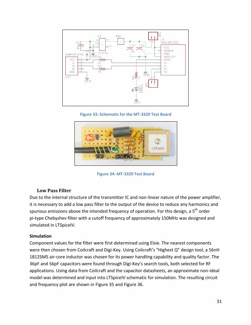
Figure 33: Schematic for the MT-3329 Test Board ....................................................................... 31
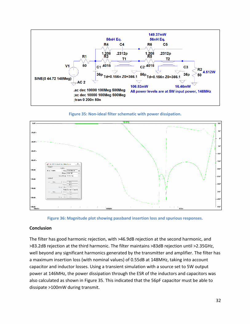
Figure 34: MT-3329 Test Board .................................................................................................... 31
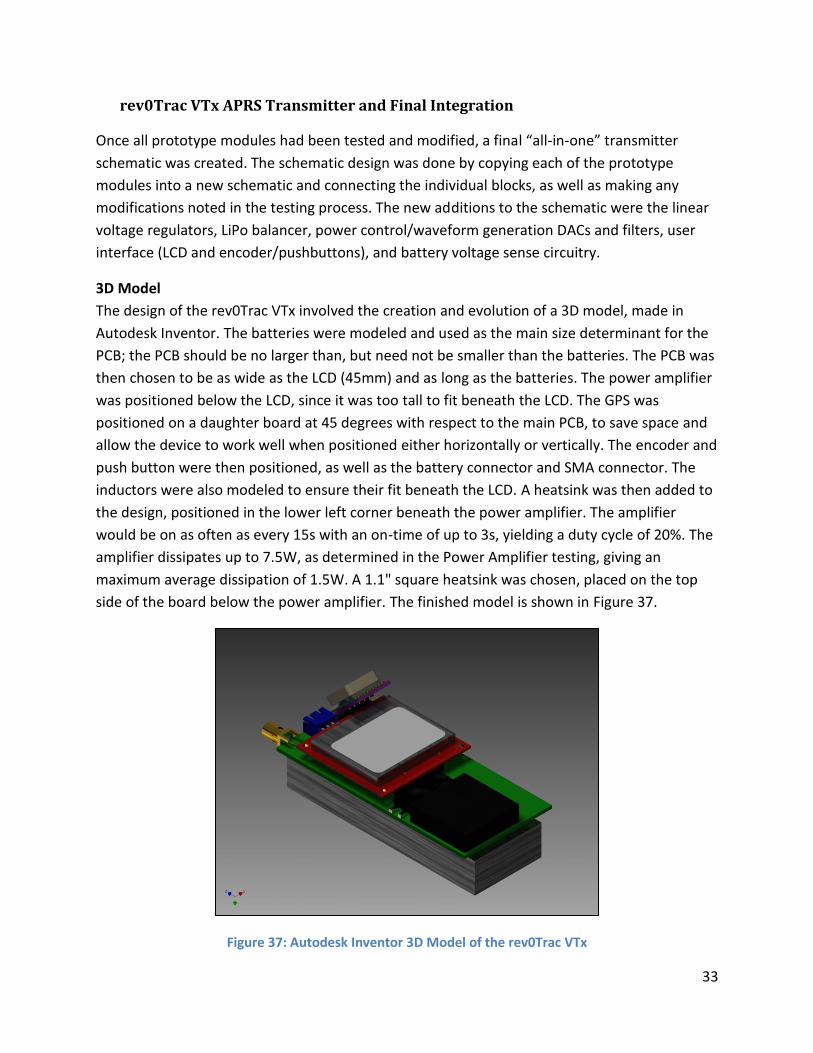
Figure 35: Non-ideal filter schematic with power dissipation. ..................................................... 32
Figure 36: Magnitude plot showing passband insertion loss and spurious responses. ............... 32
Figure 37: Autodesk Inventor 3D Model of the rev0Trac VTx ...................................................... 33
Figure 38: rev0Trac VTx v1.0 Schematic ....................................................................................... 35
Figure 39: rev0Trac VTx v1.0 PCB Layout...................................................................................... 36
Figure 40: Bare and partially-soldered rev0Trac VTx PCBs ........................................................... 37
Figure 41: 1200Hz tone before and after the low pass filter ....................................................... 38
Figure 42: 2200Hz tone before and after the low pass filter ....................................................... 38
Figure 43: Tone burst of 1200Hz/2200Hz tones after the low pass filter .................................... 39
Figure 44: Test Setup for Measuring rev0Trac VTx Output Power/Spectra ................................. 40
Figure 45: Final working rev0Trac VTx APRS Transmitter ............................................................. 41
Figure 46: Revised rev0Trac VTx Schematic ................................................................................. 49
Figure 47: Revised rev0Trac VTx PCB Layout ................................................................................ 50

v
ABSTRACT
The Automatic Packet Reporting System (APRS) is a digital radio system that allows
transmission of data using an analog FM radio link. APRS allows position, brief messages, and
other data to be distributed across a network, independent of infrastructure, making it ideal for
applications such as search and rescue, asset management, and event tracking, while
maintaining low cost and operating even when cellular and internet services are unavailable.
This project encompasses the design, build, and test of a compact, low-cost APRS transmitter,
which will include a 5W radio, GPS, and LCD-based user interface, to allow full utilization of
APRS.

vi
ACKNOWLEDGEMENTS
I would like to thank my professors and faculty in the EE department who have made my
education what it is today, my friends and family for supporting me throughout my college
career, and my advisor, Dr. John Saghri for giving me the opportunity to work on this project.

1
I. Introduction
This project was conceived as an improvement on currently available APRS trackers. There are
three basic classes of APRS devices: trackers, which contain only the hardware to generate
audio packets from an incoming data stream (e.g. from a computer or external GPS module);
transmitters, which contain a built in radio in addition to the packet generator, and may or may
not contain a built in GPS; and transceivers, which contain all functionality of transmitters with
the addition of being able to receive packets. As of 2012, there are many trackers and several
transmitters, but few transceivers available on the market. Of the common all-in-one
transmitters, none have a built in user interface, and require that the device be pre-
programmed with settings and information before use. This project aims to create a simple, low
cost APRS transmitter with built in GPS and LCD, enabling configuration without the need of a
computer.
The data transmitted by an APRS tracker may be decoded directly with the aid of an FM
receiver and either a computer or terminal node controller (TNC), which performs the job of
decoding the incoming packets either with software through a computer sound card, or with
hardware/software in the TNC. The APRS network is composed of digipeaters, which are
transceivers which receive packets, determine whether the packet should be repeated based
on its path settings, and retransmits if necessary. The APRS network also contains IGates, which
are receivers or digipeaters that are connected to a networked computer, thus able to send the
packet over the APRS internet system (APRS-IS). These packets can be viewed online and
plotted on maps in real time. Figure 1 shows packets viewed online and received locally.
Figure 1: APRS packets on online map (top), and received directly (bottom)
2
II. Background
APRS History
The history of APRS began in 1974 with the release of the AX.25 specification. Bob Bruninga,
the creator of APRS, began with the creation of a computer system that would decode Navy
position reports and plot them. The system was later modified and used with the AX.25
protocol in 1984, then called the Connectionless Emergency Traffic System (CERT) [1]. Bob
Bruninga published the first paper on APRS in 1993, describing the system widely used today.
APRS Technical Details
APRS is based on the AX.25 packet protocol, which defines the link layer for a communications
system [2]. APRS uses AX.25 unconnected information (UI) frames to transmit data between
multiple stations, and defines several message types that can be used. The most widely used
implementation of APRS uses audio tones sent over an analog FM radio, typically operating in
the VHF amateur band.
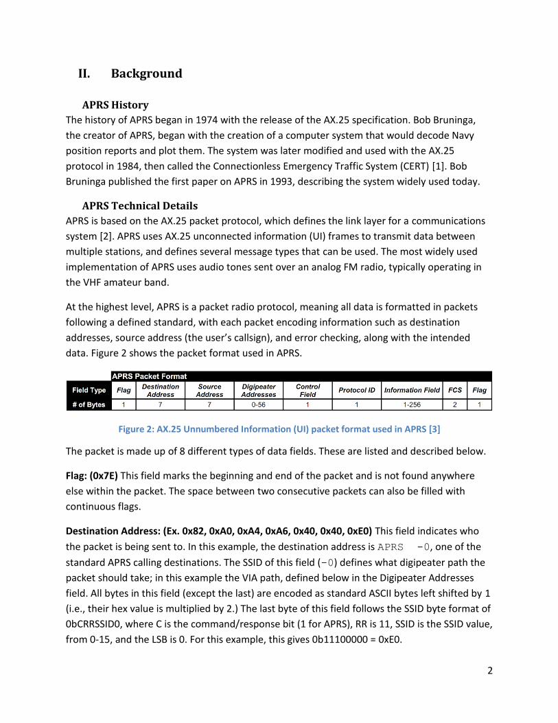
At the highest level, APRS is a packet radio protocol, meaning all data is formatted in packets
following a defined standard, with each packet encoding information such as destination
addresses, source address (the user’s callsign), and error checking, along with the intended
data. Figure 2 shows the packet format used in APRS.
Figure 2: AX.25 Unnumbered Information (UI) packet format used in APRS [3]
The packet is made up of 8 different types of data fields. These are listed and described below.
Flag: (0x7E) This field marks the beginning and end of the packet and is not found anywhere
else within the packet. The space between two consecutive packets can also be filled with
continuous flags.
Destination Address: (Ex. 0x82, 0xA0, 0xA4, 0xA6, 0x40, 0x40, 0xE0) This field indicates who
the packet is being sent to. In this example, the destination address is APRS -0, one of the
standard APRS calling destinations. The SSID of this field (-0) defines what digipeater path the
packet should take; in this example the VIA path, defined below in the Digipeater Addresses
field. All bytes in this field (except the last) are encoded as standard ASCII bytes left shifted by 1
(i.e., their hex value is multiplied by 2.) The last byte of this field follows the SSID byte format of
0bCRRSSID0, where C is the command/response bit (1 for APRS), RR is 11, SSID is the SSID value,
from 0-15, and the LSB is 0. For this example, this gives 0b11100000 = 0xE0.

3
Source Address: (Ex. 0x96, 0x94, 0x6C, 0x96, 0xA6, 0xA8, 0xE2) This field indicates who the
packet is being sent from. In this example, the source address is the author’s callsign,
KJ6KST-1. A user may have up to 16 (-0 to -15) different APRS stations on the air, each with
different SSIDs. [4] All bytes in this field are left shifted by 1, with the last byte following the
SSID byte format listed above.
Digipeater Addresses: (Ex. 0xAE, 0x92, 0x88, 0x8A, 0x62, 0x40, 0x63) This field is a list of the
digipeater addresses (call signs) or indicates a generic path for the packet to follow. In this
example, the generic path WIDE1-1 is used, meaning it will be repeated in one “hop”, with
each digipeater decrementing the SSID until it reaches -0. The first digipeater(s) to hear this
packet will retransmit it once more for other stations or IGates to receive. The last address in
this field must end with an LSB of 1 to indicate the end of the address fields.
Control Field: (0x03) This field indicates that the packet is an unnumbered information (UI)
frame, the default for APRS.
Protocol ID: (0xF0) This field indicates that there is no layer 3 (network layer) implementation,
as is standard for APRS.
Information Field (Ex. 0x21, 0x30, 0x30, 0x30, 0x30, 0x2E, 0x30, 0x30, 0x4E, 0x2F, 0x30, 0x30,
0x30, 0x30, 0x30, 0x2E, 0x30, 0x30, 0x57, 0x3E) This field contains the information the user
wants to send, following one of the ten main types of data as defined in the APRS specification.
In this example, the information field contains a basic GPS position report:
(!0000.00N/00000.00W>). This field begins with the “!” character, and ends with the “>”
character. The “/” character between the latitude and longitude defines what symbol table the
station uses (primary: “/” or secondary: “\”), and the “>” character defines which symbol in the
table is used; in this example, a car. A list of these symbols is found in the APRS specification.
The information field can be followed by a comment field directly after the data, and may
include any characters except “|” and “~”.
Frame Check Sequence (Ex. 0x38, 0x76) This field contains a Cyclic Redundancy Check (CRC) of
all bytes in the packet except the flags and the FCS itself. The CRC follows the 16-bit CRC-CCITT
format, with a polynomial of 0x8408. The FCS is sent low-byte first.
Flag (0x7E) The end of the packet is marked by another flag.
APRS packets are transmitted over the air using the modulation scheme of a Bell 202 modem,
called AFSK (Audio Frequency-Shift Keying), at a baud rate of 1200 (bits per second). The
modulation is most commonly used over an analog FM radio link, but single sideband (SSB) and
Gaussian frequency shift keying (GFSK) modulations are also used at 300 and 9600 baud. The
Bell 202 modem uses two audio tones of different frequencies to represent binary 1 and 0, with
4
a 1200Hz tone as the mark (1) bit, and a 2200Hz tone as the space (0) bit. However, if data were
sent without further encoding, certain strings of data may create an unintentional flag (0x7E),
which would be seen to the receiver as the end of the packet. To prevent this problem from
occurring, a scheme called bit stuffing is used. Any time a sequence of 5 consecutive 1s are seen
in the data, a 0 is inserted, ensuring that no flags (sequence of six 1s) are found anywhere but
the beginning and end of the packet. To assist with receiver synchronization, the packet is non-
return to zero inverted (NRZI) encoded. This encodes a 0 as a change in state (i.e. from a 0 to a
1 or from a 1 to a 0), and a 1 as no change in state. Together with bit stuffing, this ensures that
there is a bit transition at least every 5 bits to aid in clock recovery. Unlike bit stuffing, NRZI
encoding is applied to the entire packet, including flags and FCS. All bytes are sent least
significant bit (LSB) first.
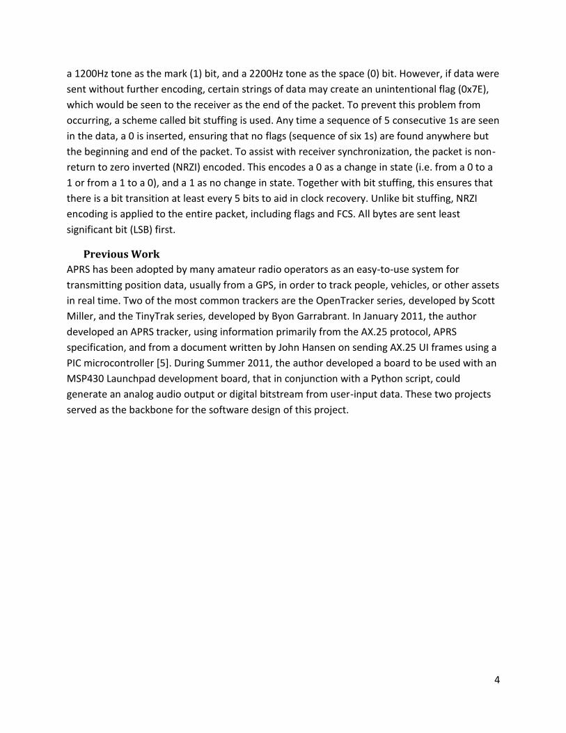
Previous Work
APRS has been adopted by many amateur radio operators as an easy-to-use system for
transmitting position data, usually from a GPS, in order to track people, vehicles, or other assets
in real time. Two of the most common trackers are the OpenTracker series, developed by Scott
Miller, and the TinyTrak series, developed by Byon Garrabrant. In January 2011, the author
developed an APRS tracker, using information primarily from the AX.25 protocol, APRS
specification, and from a document written by John Hansen on sending AX.25 UI frames using a
PIC microcontroller [5]. During Summer 2011, the author developed a board to be used with an
MSP430 Launchpad development board, that in conjunction with a Python script, could
generate an analog audio output or digital bitstream from user-input data. These two projects
served as the backbone for the software design of this project.

5
III. Requirements and Specifications
The APRS Transceiver fulfills the following specifications as defined by the project goals; to
capture and transmit GPS coordinates using the APRS protocol, display GPS data and device
status, and operate according to FCC regulations and frequency allocations.
Table 1: All-In-One APRS Transmitter Requirements and Specifications
Marketing
Requirements
Engineering
Specifications Justification
1, 2 Contains radio transmitter operating in the
amateur 2M band to transmit APRS data at a
duty cycle no greater than 10% with a power
of up to 5W
Must have a sufficient transmit power to cover a
large area. APRS packets are typically sent at a
low duty cycle, e.g. once per 15-30 seconds, to
minimize network usage.
1, 2 Can operate for at least 6 hours transmitting
APRS position data at a rate of once per 15
seconds
Must be able to operate for a sufficient time
before requiring a recharge.
3 Fits 12 x 5 x 4 cm, and weighs less than
180g
Must be compact and lightweight to not hinder
the user.
4 Uses USB for PC interface and charging Needs to use standard interface to receive
firmware updates and charge the battery.
5 Displays current position and status on built
in LCD display
Allows the user to change settings and get
current location and battery status without the
use of a computer.
6 Spurious emissions must not exceed -40dBc
or 25µW [6]
Must comply with the FCC Part 97 emissions
standards for amateur radio transmitters.
Marketing
Requirements
1. Transmit APRS data at high power
2. Long battery life
3. Low weight/size
4. Interface with computer for firmware upgrade and charging
5. Displays position and device status
6. Meets FCC Part 97 requirements

6
IV. Design
This project was designed through a series of prototypes, each testing an individual building
block of the final transmitter. This enables each module to be tested more easily over a wider
range of parameters, and facilitates changes before the system grows too complex. Once each
module is tested and working to specifications, it can be integrated into the complete system.
The overall system block diagram is shown in Figure 3, which shows the six basic building blocks
of the transmitter (excluding the LCD). The following sections describe the development and
testing of each of these blocks.
Figure 3: All-In-One APRS Transmitter Block Diagram
MICRF112 Transmitter
This module is a test board for the MICRF112 433MHz transmitter IC, manufactured by Micrel.
The circuit is based on the example circuit given in the datasheet. After performing a basic
functional test of the device, the circuit was modified to allow tuning of the reference crystal by
means of a variable capacitor. After determining the frequency vs. voltage transfer
characteristic using a spectrum analyzer and power supply, the voltage needed to produce a
4.8kHz FM deviation was calculated. Using a signal generator, 400Hz, 1.2kHz, and 2.2kHz
modulating tones were then applied and the FM spectra were measured using a spectrum
analyzer.

7
Circuit Schematic and Theory
The MICRF112 is a single-chip ASK/FSK transmitter IC designed for short range wireless devices.
[7] Short range devices (SRDs) are defined by the European Telecommunications Standards
Institude (ETSI) as “radio devices that offer a low risk of interference with other radio services,
usually because their transmitted power, and hence their range, is low.” [8] There are many
similar devices available for the SRD market, usually containing an on-board PLL, VCO, and
control circuitry. The simplicity of their operation and widespread use makes these a good low-
cost solution for generating analog FM in a transmit-only application. This device allows data to
be transmitted via amplitude shift keying (ASK) or frequency shift keying (FSK) via two pins. RF
is generated by a fixed on-board 32x PLL, using an external crystal or reference frequency as the
input. An internal power amplifier provides an output power of up to 10dBm. A block diagram
for the device is shown in Figure 4.
Figure 4: MICRF112 Functional Block Diagram [7]
The circuit schematic (shown in Figure 5) is based on the application circuit given in the device
datasheet. A 13.56MHz crystal was chosen for the device to transmit on 433.92MHz. The
datasheet suggested matching network was used to match the device to 50Ω, connecting to an
SMA port. Power, ground, and the ASK pin (used as transmit/device enable) are routed to
external pins, and a test point and SMA port are routed the crystal input and output,
respectively.

8
Figure 5: MICRF112 Test Board Schematic
The circuit was then modified to allow modulation of the reference frequency by pulling the
crystal oscillator through the load capacitors, C1 and C2. A varactor diode replaces C1, with the
tuning voltage being applied through a 10kΩ resistor. The resistor value was chosen empirically
for the highest FM deviation. The varactor diode was chosen based on availability and
capacitance range. The device used is a Philips BAT754 dual Schottky diode. A graph of the
capacitance vs. reverse voltage is shown in Figure 6.
Figure 6: BAT754 Diode Capacitance vs. Reverse Voltage [9]
Using both diodes in the BAT754 in parallel, a capacitance range of approximately 20pF to 5pF
could be achieved using a 0-5V tuning voltage. This is within the range of load capacitance
needed by the 13.56MHz reference crystal. The modified circuit is shown in Figure 7, and the
modified PCB is shown in Figure 8.

9
Figure 7: Modified MICRF112 Test Board Schematic
Figure 8: Modified MICRF112 Test Board
Testing
A table of frequency vs. tuning voltage was recorded using an HP 8922M spectrum analyzer to
measure carrier frequency while varying the tuning voltage using a power supply. A graph
summarizing the results is shown in Figure 9.

10
Figure 9: Frequency vs. Tuning Voltage Transfer Characteristic
A logarithmic regression was applied to the data to obtain a curve with the following formula:
Where v is the tuning voltage in volts, and F(v) is the resulting frequency. Taking a derivative
results in the FM deviation vs. bias voltage of the overall system:
A typical VHF/UHF FM transceiver uses a deviation of 4.8kHz when transmitting voice, thus
4.8kHz was chosen as the desired deviation. A bias voltage of 2.5V was chosen to remain within
the power rails of 0-3.6V and to provide the best linearity within the tuning range (a higher bias
voltage yields a more linear slope, as seen in Figure 9.) Using the derivative at 2.5V yields a
required voltage swing of 1.03Vp-p for the desired deviation. Thus the minimum and maximum
voltages are 1.99 and 3.01V. Solving for frequency using the first formula yields and actual
minimum and maximum frequency of 433.9243 and 433.9291MHz, giving an actual deviation of
4.87kHz, close to the linear estimate. The linear estimate is overlaid on the graph in order to
visualize the error over the range of 1-4V. A signal generator was used to produce 400Hz,
1.2kHz and 2.2kHz tones with a 1.03Vp-p amplitude at 2.5V DC offset. The spectra were then
measured as shown in Figure 10.
11
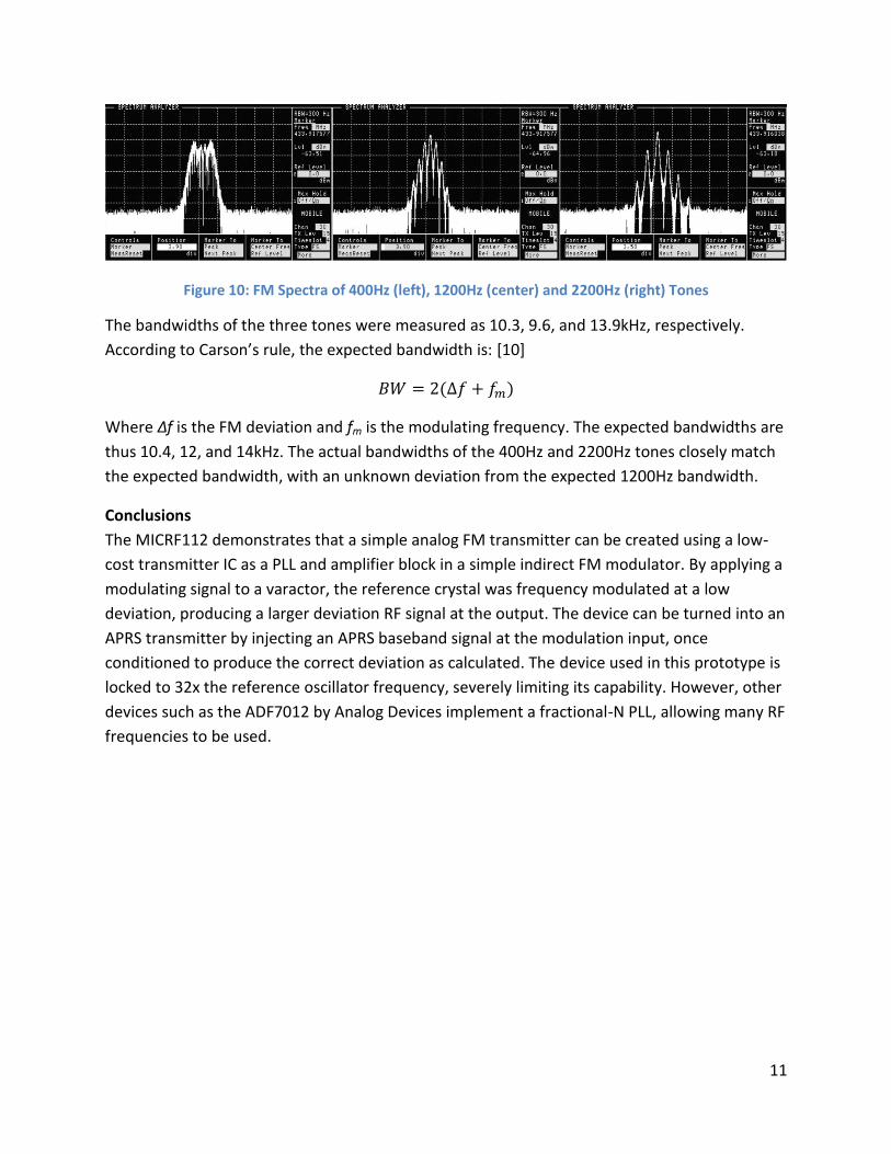
Figure 10: FM Spectra of 400Hz (left), 1200Hz (center) and 2200Hz (right) Tones
The bandwidths of the three tones were measured as 10.3, 9.6, and 13.9kHz, respectively.
According to Carson’s rule, the expected bandwidth is: [10]
Where ∆f is the FM deviation and fm is the modulating frequency. The expected bandwidths are
thus 10.4, 12, and 14kHz. The actual bandwidths of the 400Hz and 2200Hz tones closely match
the expected bandwidth, with an unknown deviation from the expected 1200Hz bandwidth.
Conclusions
The MICRF112 demonstrates that a simple analog FM transmitter can be created using a low-
cost transmitter IC as a PLL and amplifier block in a simple indirect FM modulator. By applying a
modulating signal to a varactor, the reference crystal was frequency modulated at a low
deviation, producing a larger deviation RF signal at the output. The device can be turned into an
APRS transmitter by injecting an APRS baseband signal at the modulation input, once
conditioned to produce the correct deviation as calculated. The device used in this prototype is
locked to 32x the reference oscillator frequency, severely limiting its capability. However, other
devices such as the ADF7012 by Analog Devices implement a fractional-N PLL, allowing many RF
frequencies to be used.

12
ADF7012 Transmitter
The ADF7012 is a single-chip ASK/FSK transmitter IC supporting multiple modulation types and
integrating a fractional-N PLL, allowing the transmit frequency to be selected by an external
microcontroller. Similarly to the MICRF112, the ADF7012 is designed for digital modulations via
clock and data pins on the device, with the carrier generated by a PLL with a crystal oscillator as
the reference. The device is capable of 14dBm output power and covers a frequency range of
75MHz to 1GHz via the PLL and output divider. The test board provides a low-pass filter, access
to the SPI bus, and control voltage for an external 20MHz VCXO, which is used as the reference.
The schematic for this test board, again based on the example circuit given in the datasheet, is
shown in Figure 11, and the layout is shown in Figure 12.
Figure 11: Schematic for the ADF7012 Test Board
13
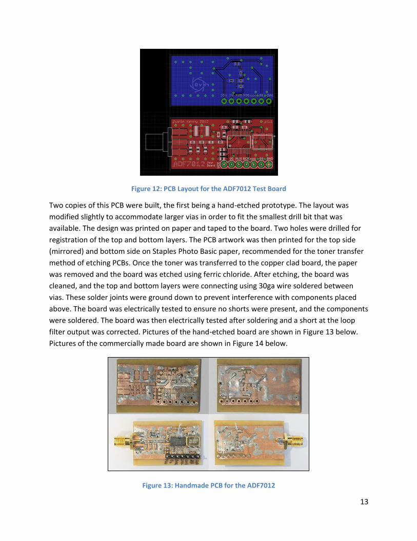
Figure 12: PCB Layout for the ADF7012 Test Board
Two copies of this PCB were built, the first being a hand-etched prototype. The layout was
modified slightly to accommodate larger vias in order to fit the smallest drill bit that was
available. The design was printed on paper and taped to the board. Two holes were drilled for
registration of the top and bottom layers. The PCB artwork was then printed for the top side
(mirrored) and bottom side on Staples Photo Basic paper, recommended for the toner transfer
method of etching PCBs. Once the toner was transferred to the copper clad board, the paper
was removed and the board was etched using ferric chloride. After etching, the board was
cleaned, and the top and bottom layers were connecting using 30ga wire soldered between
vias. These solder joints were ground down to prevent interference with components placed
above. The board was electrically tested to ensure no shorts were present, and the components
were soldered. The board was then electrically tested after soldering and a short at the loop
filter output was corrected. Pictures of the hand-etched board are shown in Figure 13 below.
Pictures of the commercially made board are shown in Figure 14 below.
Figure 13: Handmade PCB for the ADF7012
14
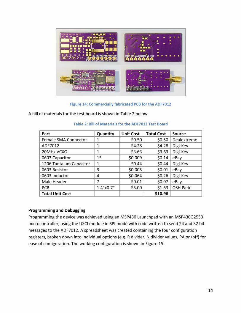
Figure 14: Commercially fabricated PCB for the ADF7012
A bill of materials for the test board is shown in Table 2 below.
Table 2: Bill of Materials for the ADF7012 Test Board
Part Quantity Unit Cost Total Cost Source
Female SMA Connector 1 $0.50 $0.50 Dealextreme
ADF7012 1 $4.28 $4.28 Digi-Key
20MHz VCXO 1 $3.63 $3.63 Digi-Key
0603 Capacitor 15 $0.009 $0.14 eBay
1206 Tantalum Capacitor 1 $0.44 $0.44 Digi-Key
0603 Resistor 3 $0.003 $0.01 eBay
0603 Inductor 4 $0.064 $0.26 Digi-Key
Male Header 7 $0.01 $0.07 eBay
PCB 1.4”x0.7” $5.00 $1.63 OSH Park
Total Unit Cost $10.96
Programming and Debugging
Programming the device was achieved using an MSP430 Launchpad with an MSP430G2553
microcontroller, using the USCI module in SPI mode with code written to send 24 and 32 bit
messages to the ADF7012. A spreadsheet was created containing the four configuration
registers, broken down into individual options (e.g. R divider, N divider values, PA on/off) for
ease of configuration. The working configuration is shown in Figure 15.

15
Figure 15: Configuration register worksheet and working values.
The first step in verifying the board’s functionality was applying power after checking for shorts,
and verifying the quiescent current of the device. The VCXO output was then verified with an
oscilloscope to ensure the proper 20MHz output. The SPI code was first tested by viewing the
waveform on the oscilloscope and using a known good SPI LCD to ensure no software errors.
The ADF7012 was then initialized and the MUXOUT pin was selected to output a divided
reference clock. The divider was modified to ensure the SPI code was working. The MUXOUT
pin was then selected to output R and N divider outputs. These were found to be different
frequencies, indicating the PLL was not able to lock. The input and output of the loop filter were
measured on the oscilloscope and it was determined that the output of the loop filter was
shorted to ground underneath the ADF7012 IC. The shorted trace was cut and the pin was
reconnected using 30ga wire to the output of the loop filter. PLL operation was then verified by
viewing the R and N divider outputs on the MUXOUT pin. Trial and error showed that the power
amplifier was enabled when setting the device to ASK mode with the data inverted bit set, since
TxData and TxClock pins were grounded by design.

16
Testing
The spectra of the ADF7012 were captured for a carrier at 146MHz, the second through fourth
harmonics, and an FM signal with 400 and 1000Hz modulating tones at 400mVp-p. The spectra
of the 400Hz tone, using -3dB points, was measured to be 7.8kHz, and the spectra of the 1kHz
tone was measured to be 7.45kHz, as shown in Figure 16.
Figure 16: FM spectra of a 400Hz (left) and 1kHz (right) tone at 400mVp-p
A table of the harmonic powers is shown in Table 3. The data shows that the 5th order low-pass
filter keeps harmonics at least 4.15dB below the FCC specification of -40dBc [11]. However,
filtering after the power amplifier will be more critical since the power amplifier will produce
additional power at the harmonics since it is operating near its compression point.
Table 3: Carrier and Harmonic Powers at 146MHz.
Frequency (MHz) Power (dBm) Power (dBc)
146 10.23 0.00
292 -40.75 -50.98
438 -33.92 -44.15
584 -71.59 -81.82
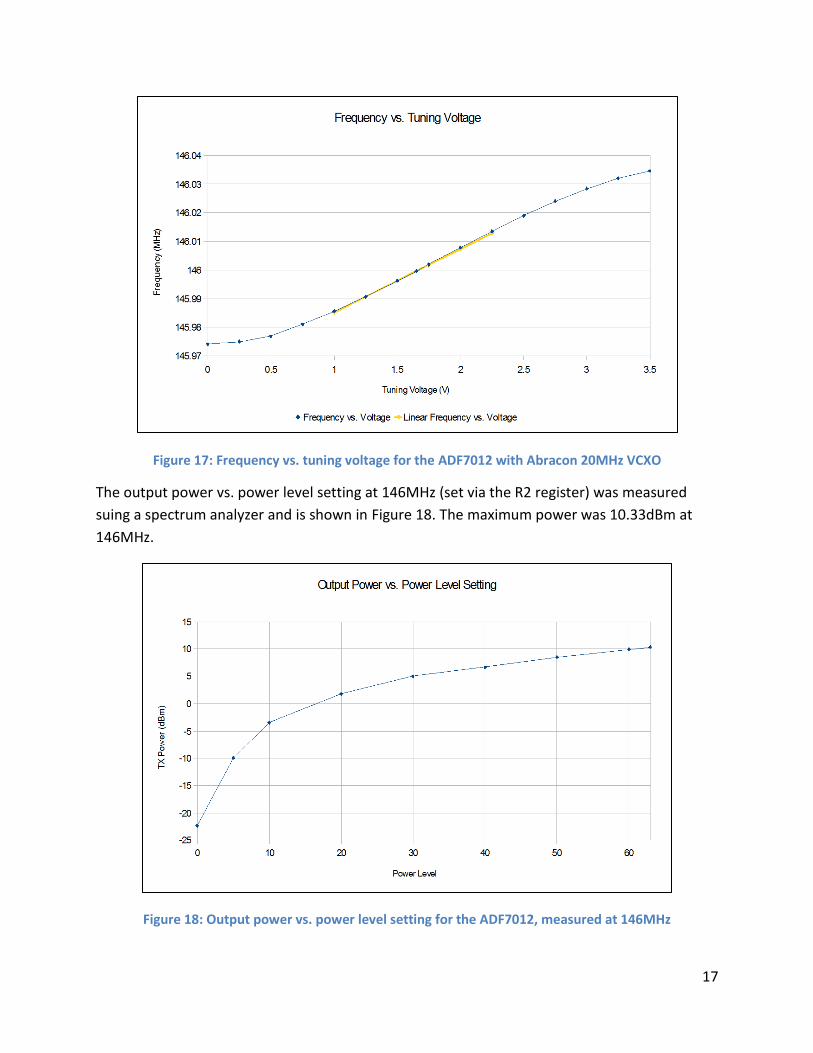
Following the procedure used with the MICRF112 test board, a plot of the frequency vs. tuning
voltage was obtained using an external power supply to bias the VCXO. The results in Figure 17
show that the VCXO has a nearly linear tuning curve, especially around a bias point near half
the supply voltage. From this data, it was determined that a 217mVp-p signal provides a 4.8kHz
FM deviation.
17
Figure 17: Frequency vs. tuning voltage for the ADF7012 with Abracon 20MHz VCXO
The output power vs. power level setting at 146MHz (set via the R2 register) was measured
suing a spectrum analyzer and is shown in Figure 18. The maximum power was 10.33dBm at
146MHz.
Figure 18: Output power vs. power level setting for the ADF7012, measured at 146MHz

18
The upper and lower ranges of the PLL, under the condition of phase noise <-20dBc, were
measured to be approximately 158MHz and 141.083MHz, yielding a total tuning range of
16.9MHz, just above the range needed to cover the amateur 2m band plus 10.7MHz for LO
generation if used in a transceiver application. However, the phase noise of this device would
be unacceptable for use in a receiver. Reducing the VCO bias to a value of 5 (2.5mA) and the
charge pump at maximum current (largest loop bandwidth) was experimentally determined to
yield the lowest phase noise.
Conclusion
The ADF7012 is a much more capable transmitter IC, capable of covering the entire 2m amateur
band as selected in the requirements for an APRS transmitter. A VCXO reference shows much
greater linearity compared to a simple crystal oscillator and varactor configuration, making FM
generation easier.

19
Power Amplifier
Two devices were under review for the power amplifier to be used in this project. The project
specification calls for a 5W 50Ω output power over the frequency range of 144-148MHz. The
first method is a design using discrete RF MOSFETs. The second method is to use a pre-
packaged power amplifier module manufactured by Mitsubishi, which integrates input/output
matching. An application note for a 135-175MHz amplifier using the STMicroelectronics
PD54008 and PD84001 MOSFETs was used for the schematic design. [12] The application note
included full schematics, board layout, and test data for the complete amplifier. From the
provided schematics, a PCB was designed for the STMicroelectronics amplifier, and a cost
comparison was performed against the Mitsubishi amplifier module.
STMicroelectronics Amplifier
The PD54008 is an N-channel RF MOSFET capable of 8W output power with 11.5dB gain at
500MHz. [13] The PD84001 is an N-channel RF MOSFET capable of 1W output power with 15dB
gain at 870MHz. [14] The test board provides all necessary matching, DC biasing, and output
filtering. The schematic for this test board is shown in Figure 19, and the board is shown in
Figure 20.
Figure 19: Schematic for the ST Power Amplifier Test Board

20
Figure 20: PCB Layout for the ST Power Amplifier Test Board
A bill of materials for the board is shown in Table 4. The total cost for a power amplifier module
using the STMicroelectronics MOSFETs including a low-pass filter is $28.38.
Table 4: Bill of Materials for the STMicroelectronics Power Amplifier Board
Part Quantity Unit Cost Total Cost Source
PD54008 1 $7.50 $7.50 Digi-Key
PD84001 1 $3.19 $3.19 Digi-Key
SMA Female Connector 2 $0.50 $1.00 Dealextreme
0603 Capacitor 23 $0.009 $0.22 eBay
0603 Resistor 6 $0.003 $0.02 eBay
0603Hc-18NX 1 $0.79 $0.79 Coilcraft
1008CS-xxxX 3 $0.79 $2.37 Coilcraft
1812SMS-22N 2 $0.95 $1.90 Coilcraft
A05T 1 $0.91 $0.91 Coilcraft
Male Header 5 $0.01 $0.05 eBay
PCB 2.075”x0.875” $5.00 $3.03 OSH Park
Total Unit Cost $28.38
Mitsubishi Amplifier
The RA07M1317M MOSFET amplifier module is a two-stage amplifier capable of outputting
6.5W with approximately 35dB gain, internally matched to 50Ω over the frequency range of
135-175MHz. [15] The test board provides two SMA connectors and bypassing capacitors for
the gate and drain voltage inputs to the module. The schematic for this test board is shown in
Figure 21, and the board is shown in Figure 22.

21
Figure 21: Schematic for the Mitsubishi Power Amplifier Test Board
Figure 22: PCB Layout for the Mitsubishi Power Amplifier Test Board
A bill of materials for the Mitsubishi power amplifier test board is shown in Table 5.
Table 5: Bill of Materials for the Mitsubishi Power Amplifier Test Board
Part Quantity Unit Cost Total Cost Source
RA07M1317M 1 $19.95 $19.95 RFParts
SMA Female Connector 2 $0.50 $1.00 Dealextreme
0603 Capacitor 2 $0.009 $0.02 eBay
3216 Tantalum Capacitor
2 $0.64 $1.28 Digi-Key
Male Header 3 $0.01 $0.03 eBay
PCB 1.35”x0.95” $5.00 $2.14 OSH Park
Total Unit Cost $24.42
Although the test board does not include the low-pass filter, the Mitsubishi amplifier has a
lower overall cost and required board area, and the complexity is reduced by a significant

22
margin. Based on these criteria, the Mitsubishi amplifier was chosen to be built and tested for
use in the final transmitter.
Testing
The amplifier was tested using an HP 8922M GSM Test Set, using the Aux. RF Output supplying
0-9dBm at 144-148MHz, while reading the RF OUT power through the RF In/Out port on the
Test Set. VDD was supplied at 6-8.4V, the working voltage range of a 2-cell lithium polymer
battery pack, through an HP 6284A power supply. VGG was supplied at 0-3.5V using a power
supply and potentiometer. Gate voltage was monitored using an HP 3466A multimeter, and
current was read from the built-in meter of the 6284A. The output power, gain, and efficiency
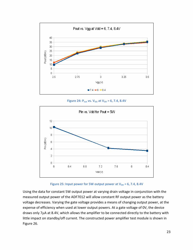
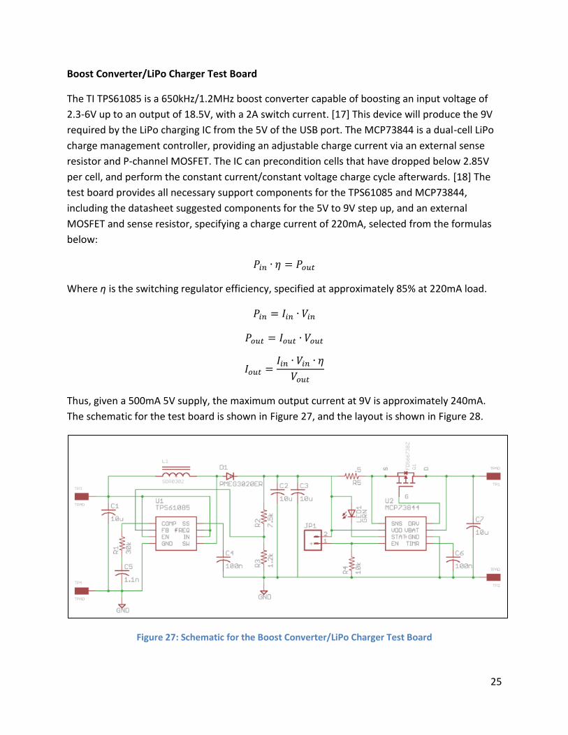
vs. gate voltage is shown in Figure 23. The output power vs. gate voltage at drain voltages of 6,
7.4, and 8.4V is shown in Figure 24. The input power for a fixed 5W power output at drain
voltages of 6, 7.4, and 8.4V is shown in Figure 25.
Figure 23: Pout, Gain, and Efficiency vs. VGG at VDD = 7.4V
23
Figure 24: Pout vs. VGG at VDD = 6, 7.4, 8.4V
Figure 25: Input power for 5W output power at VDD = 6, 7.4, 8.4V
Using the data for constant 5W output power at varying drain voltage in conjunction with the
measured output power of the ADF7012 will allow constant RF output power as the battery
voltage decreases. Varying the gate voltage provides a means of changing output power, at the
expense of efficiency when used at lower output powers. At a gate voltage of 0V, the device
draws only 7μA at 8.4V, which allows the amplifier to be connected directly to the battery with
little impact on standby/off current. The constructed power amplifier test module is shown in
Figure 26.

24
Figure 26: Mitsubishi Power Amplifier Test Board
Conclusions
The Mitsubishi amplifier meets the project specifications and remains the simplest and
cheapest solution for this project. Although the discrete solution may result in lower costs per
board at volume, this project benefits from the simplicity and board space savings of the
Mitsubishi amplifier module.
Boost Converter and LiPo Battery Charger
The product requirements state that the device must operate on battery for at least 6 hours
transmitting a packet once every 15 seconds, the required battery size can be calculated. The
maximum transmit current was determined from the power amplifier module testing to be
1.42A. The duty cycle of the device can be calculated using assumptions about an APRS packet.
An APRS position packet with no comment and a generic path contains 47 bytes, plus a
preamble of 10 bytes. At 1200 baud, the time this packet takes to transmit is calculated below:
Taking into an additional 0.5s for the receiving radio to open squelch, plus 0.25s after ceasing
transmission, the total time is then 1.13s. For a worst-case estimate, assume 3s of transmit
every 15s period. This yields a duty cycle of 3/15 = 20%. The average current draw, assuming a
worst-case 80mA standby current is then calculated below:
The necessary battery life is then calculated below:
Based on availability and physical size, a 2-cell 2.2AH lithium polymer (LiPo) battery was chosen.
Lithium polymer batteries require special charging circuitry to deliver a constant-
current/constant-voltage charge cycle. Since the device will be charged from a standard USB
port, the charging voltage must be obtained from the USB maximum of 5V at 500mA. [16]
25
Boost Converter/LiPo Charger Test Board
The TI TPS61085 is a 650kHz/1.2MHz boost converter capable of boosting an input voltage of
2.3-6V up to an output of 18.5V, with a 2A switch current. [17] This device will produce the 9V
required by the LiPo charging IC from the 5V of the USB port. The MCP73844 is a dual-cell LiPo
charge management controller, providing an adjustable charge current via an external sense
resistor and P-channel MOSFET. The IC can precondition cells that have dropped below 2.85V
per cell, and perform the constant current/constant voltage charge cycle afterwards. [18] The
test board provides all necessary support components for the TPS61085 and MCP73844,
including the datasheet suggested components for the 5V to 9V step up, and an external
MOSFET and sense resistor, specifying a charge current of 220mA, selected from the formulas
below:
Where η is the switching regulator efficiency, specified at approximately 85% at 220mA load.
Thus, given a 500mA 5V supply, the maximum output current at 9V is approximately 240mA.
The schematic for the test board is shown in Figure 27, and the layout is shown in Figure 28.
Figure 27: Schematic for the Boost Converter/LiPo Charger Test Board
26
Figure 28: PCB Layout for the Boost Converter/LiPo Charger Test Board
Testing
The boost converter and charger IC were tested, with results summarized in Table 6 below.
Table 6: Boost Converter/LiPo Charger Summary of Test Results
Output Voltage 9.009V
Charge Current 212.3mA
Charge Termination Voltage 8.382V
Output Power 1.913W
Input Voltage 4.974V
Input Current 437.5mA
Input Power 2.176W
Efficiency 87.9%
Heat Power 263mW
Reverse Leakage Current (Charger disabled) 0.2μA
Reverse Leakage Current (Charger unpowered) 895μA
The results show that the charger/boost converter produce the necessary voltages to function
(within 0.2%), and maintain a current draw of less than 500mA at the full charge current, as
required by USB. [16] Additionally, the reverse leakage current is negligible (a concern for
battery drain when in use and when the device is off). The boost converter has an efficiency of
87.9%, higher than the datasheet’s specification, so little power is wasted as heat. The
constructed PCB is shown in Figure 29.The bill of materials for the device is shown in Table 7.

27
Figure 29: Boost Converter/LiPo Charger PCB
Table 7: Bill of Materials for the Boost Converter/LiPo Charger
Part Quantity Unit Cost Total Cost Source
TPS61085DGKT 1 $3.30 $3.30 Digi-Key
MCP73844-840I/MS 1 $1.56 $1.56 Digi-Key
0603 Capacitor 3 $0.009 $0.03 eBay
0603 Resistor 5 $0.003 $0.02 eBay
1206 10uF Capacitor 4 $0.30 $1.19 Digi-Key
PMEG3020ER 1 $0.48 $0.48 Digi-Key
STS5PF20V 1 $0.24 $0.24 Digi-Key
0603 Green LED 1 $0.11 $0.11 Digi-Key
SDR0302-3R3ML 1 $0.42 $0.42 Digi-Key
Male Header 3 $0.01 $0.03 eBay
PCB 1.225"x0.5125" $5.00 $1.05 OSH Park
Total Unit Cost $8.43
Conclusion
Both devices in this test board meet the need of this project, namely charging the battery over
USB at a reasonably high efficiency. Since the device uses a 2-cell LiPo, a cell balancing solution
is also recommended to prevent either cell from dropping below 3V or exceeding 4.2V. An IC is
available from TI to perform this task and is used in the final transmitter.

28
Microcontroller
The system will be controlled by an MSP430F5510 microcontroller. This microcontroller was
selected due to previous experience with MSP430 microcontrollers, and for its memory size and
peripheral set. The MSP430F5510 is a 16-bit microcontroller featuring 32kB of program
memory, 4kB of program SRAM, two timers with multiple compare registers, a USCI module
supporting I2C, SPI, and UART, a 10-bit ADC, and USB functionality. [19] These features will be
utilized in the final transmitter, with applications including reading the battery voltage,
interfacing with the GPS module, LCD, RF transmitter, PC, and generating the transmit analog
waveforms. The test board provides access to the four main I/O ports, JTAG and Spy-Bi-Wire
programming ports, and necessary support components and connector for USB. The board also
includes a button and LED for basic user interaction. The schematic for the test board is shown
in Figure 30, and the layout is shown in Figure 31.
Figure 30: Schematic for the MSP430F5510 Test Board

29
Figure 31: PCB Layout for the MSP430F5510 Test Board
The device contains a USB bootloader by factory default. By holding down the PUR switch while
inserting a USB cable, the MSP430 bootloader is initialized, allowing a new user firmware to be
loaded. The capabilities of this device combined with the bootloader functionality and options
for future expansion make it a good choice for this project. The bill of materials is shown in
Table 8, and the constructed PCB is shown in Figure 32.
Table 8: Bill of Materials for the MSP430F5510 Test Board
Part Quantity Unit Cost Total Cost Source
MSP430F5510 1 $4.27 $4.27 Digi-Key
USB Micro B Connector 1 $0.87 $0.87 Digi-Key
0603 Capacitor 14 $0.009 $0.13 eBay
0603 Resistor 8 $0.003 $0.02 eBay
SMD Tacticle Switch 2 $0.12 $0.24 eBay
SMD 24MHz Crystal 1 $1.43 $1.43 Digi-Key
0603 Green LED 1 $0.11 $0.11 Digi-Key
0603 Red LED 1 $0.13 $0.13 Digi-Key
Male Header 36 $0.01 $0.36 eBay
PCB 1.025"x1.825" $5.00 $3.12 OSH Park
Total Unit Cost $10.68
30
Figure 32: MSP430F5510 Test Board
GPS Module
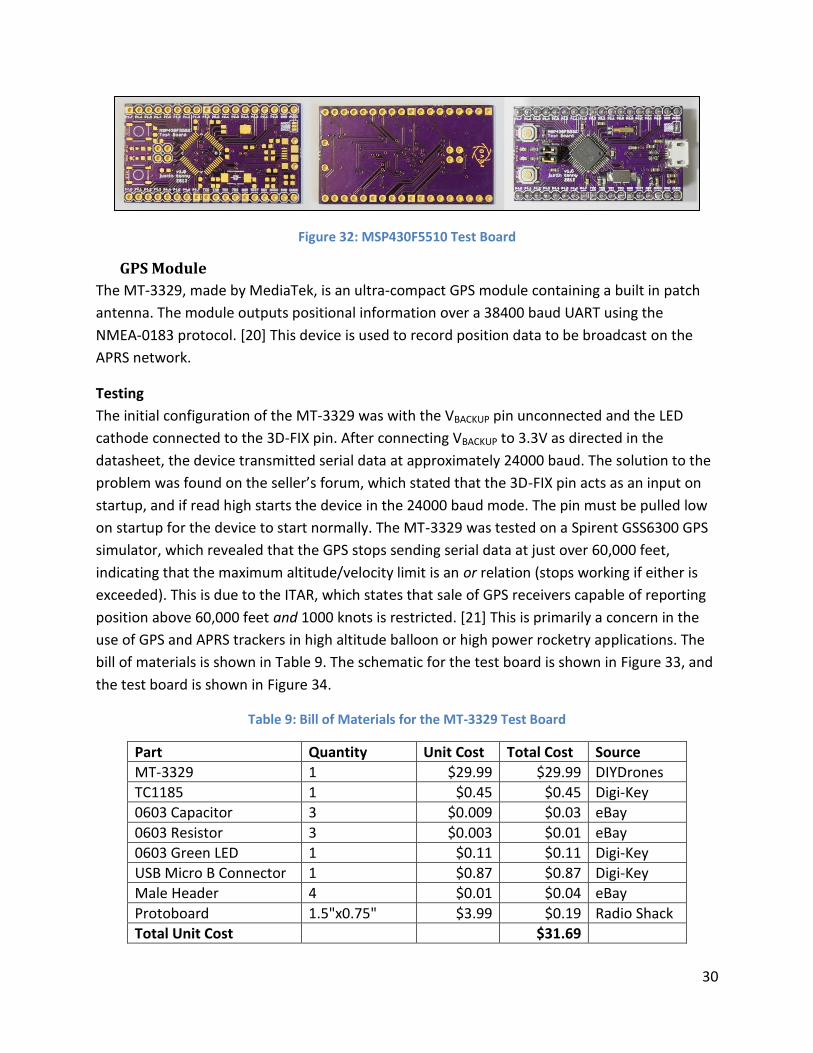
The MT-3329, made by MediaTek, is an ultra-compact GPS module containing a built in patch
antenna. The module outputs positional information over a 38400 baud UART using the
NMEA-0183 protocol. [20] This device is used to record position data to be broadcast on the
APRS network.
Testing
The initial configuration of the MT-3329 was with the VBACKUP pin unconnected and the LED
cathode connected to the 3D-FIX pin. After connecting VBACKUP to 3.3V as directed in the
datasheet, the device transmitted serial data at approximately 24000 baud. The solution to the
problem was found on the seller’s forum, which stated that the 3D-FIX pin acts as an input on
startup, and if read high starts the device in the 24000 baud mode. The pin must be pulled low
on startup for the device to start normally. The MT-3329 was tested on a Spirent GSS6300 GPS
simulator, which revealed that the GPS stops sending serial data at just over 60,000 feet,
indicating that the maximum altitude/velocity limit is an or relation (stops working if either is
exceeded). This is due to the ITAR, which states that sale of GPS receivers capable of reporting
position above 60,000 feet and 1000 knots is restricted. [21] This is primarily a concern in the
use of GPS and APRS trackers in high altitude balloon or high power rocketry applications. The
bill of materials is shown in Table 9. The schematic for the test board is shown in Figure 33, and
the test board is shown in Figure 34.
Table 9: Bill of Materials for the MT-3329 Test Board
Part Quantity Unit Cost Total Cost Source
MT-3329 1 $29.99 $29.99 DIYDrones
TC1185 1 $0.45 $0.45 Digi-Key
0603 Capacitor 3 $0.009 $0.03 eBay
0603 Resistor 3 $0.003 $0.01 eBay
0603 Green LED 1 $0.11 $0.11 Digi-Key
USB Micro B Connector 1 $0.87 $0.87 Digi-Key
Male Header 4 $0.01 $0.04 eBay
Protoboard 1.5"x0.75" $3.99 $0.19 Radio Shack
Total Unit Cost $31.69
31
Figure 33: Schematic for the MT-3329 Test Board
Figure 34: MT-3329 Test Board
Low Pass Filter
Due to the internal structure of the transmitter IC and non-linear nature of the power amplifier,
it is necessary to add a low pass filter to the output of the device to reduce any harmonics and
spurious emissions above the intended frequency of operation. For this design, a 5th order
pi-type Chebyshev filter with a cutoff frequency of approximately 150MHz was designed and
simulated in LTSpiceIV.
Simulation
Component values for the filter were first determined using Elsie. The nearest components
were then chosen from Coilcraft and Digi-Key. Using Coilcraft’s “Highest Q” design tool, a 56nH
1812SMS air-core inductor was chosen for its power handling capability and quality factor. The
36pF and 56pF capacitors were found through Digi-Key’s search tools, both selected for RF
applications. Using data from Coilcraft and the capacitor datasheets, an approximate non-ideal
model was determined and input into LTSpiceIV schematic for simulation. The resulting circuit
and frequency plot are shown in Figure 35 and Figure 36.
32
Figure 35: Non-ideal filter schematic with power dissipation.
Figure 36: Magnitude plot showing passband insertion loss and spurious responses.
Conclusion
The filter has good harmonic rejection, with >46.9dB rejection at the second harmonic, and
>83.2dB rejection at the third harmonic. The filter maintains >83dB rejection until >2.35GHz,
well beyond any significant harmonics generated by the transmitter and amplifier. The filter has
a maximum insertion loss (with nominal values) of 0.55dB at 148MHz, taking into account
capacitor and inductor losses. Using a transient simulation with a source set to 5W output
power at 146MHz, the power dissipation through the ESR of the inductors and capacitors was
also calculated as shown in Figure 35. This indicated that the 56pF capacitor must be able to
dissipate >100mW during transmit.
33
rev0Trac VTx APRS Transmitter and Final Integration
Once all prototype modules had been tested and modified, a final “all-in-one” transmitter
schematic was created. The schematic design was done by copying each of the prototype
modules into a new schematic and connecting the individual blocks, as well as making any
modifications noted in the testing process. The new additions to the schematic were the linear
voltage regulators, LiPo balancer, power control/waveform generation DACs and filters, user
interface (LCD and encoder/pushbuttons), and battery voltage sense circuitry.
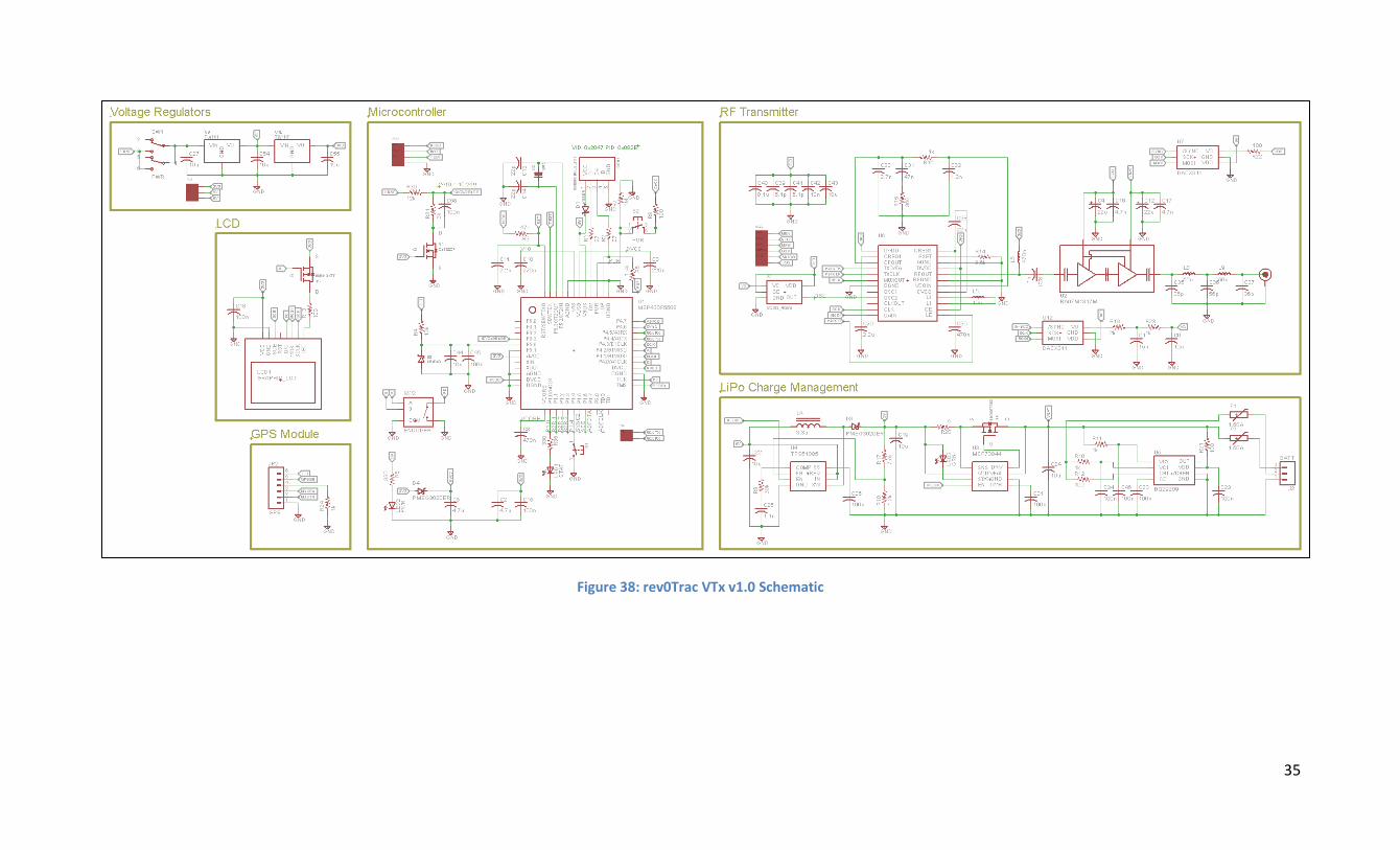
3D Model
The design of the rev0Trac VTx involved the creation and evolution of a 3D model, made in
Autodesk Inventor. The batteries were modeled and used as the main size determinant for the
PCB; the PCB should be no larger than, but need not be smaller than the batteries. The PCB was
then chosen to be as wide as the LCD (45mm) and as long as the batteries. The power amplifier
was positioned below the LCD, since it was too tall to fit beneath the LCD. The GPS was
positioned on a daughter board at 45 degrees with respect to the main PCB, to save space and
allow the device to work well when positioned either horizontally or vertically. The encoder and
push button were then positioned, as well as the battery connector and SMA connector. The
inductors were also modeled to ensure their fit beneath the LCD. A heatsink was then added to
the design, positioned in the lower left corner beneath the power amplifier. The amplifier
would be on as often as every 15s with an on-time of up to 3s, yielding a duty cycle of 20%. The
amplifier dissipates up to 7.5W, as determined in the Power Amplifier testing, giving an
maximum average dissipation of 1.5W. A 1.1" square heatsink was chosen, placed on the top
side of the board below the power amplifier. The finished model is shown in Figure 37.
Figure 37: Autodesk Inventor 3D Model of the rev0Trac VTx

34
Electrical Design
The system design follows directly from the individually tested modules. The microcontroller is
an MSP430F5510, which takes in data from the GPS and user input and controls the transmitter
IC, LCD, and amplifier. The battery is charged through the boost converter and LiPo charger IC,
which are enabled when the device is plugged into a USB port. The analog modulation signal
and gate voltage of the amplifier are controlled through a pair of 12-bit TI DAC7311 SPI digital
to analog converters, chosen for their small size and ease of interfacing. The output of the
amplifier is fed through a Chebyshev low pass filter to reduce harmonics. The final circuit was
designed for 7 mil spacing, 8 mil width, and 15 mil vias, and was manufactured by Imagineering,
Inc. The version 1.0 schematic and PCB layout are shown in Figure 38 and Figure 39.
35
Figure 38: rev0Trac VTx v1.0 Schematic
36
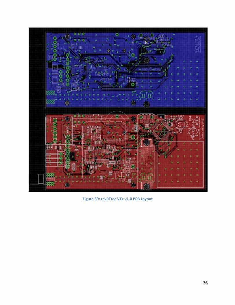
Figure 39: rev0Trac VTx v1.0 PCB Layout

37
V. Testing and Debug The microcontroller section was assembled first and the device was plugged into a computer in
bootloader mode to verify correct operation. The remainder of the board except the GPS, LCD
and PA was assembled, and power was applied to the battery input by a current-limited power
supply. The boost converter and charger IC were enabled when the device was powered from
battery, which should not have been the case. The enable lines of these devices were tied to
the USB VCC line, which is connected through a Schottky diode to the 5V line. The diode has a
specified 55μA leakage current. The enable inputs of the boost converter and charger IC are
only 0.1μA and 0.01μA, respectively, well below the leakage current. Thus, these devices were
enabled since the leakage current of the diode is more than sufficient to meet the logic high
voltage on these ICs. The solution, from ohm’s law, was to add a resistor of much less than 9.1k
ohms, which would reduce the voltage below the 1.4V necessary to act as a logic low signal to
both ICs. A 1k ohm resistor was added from the USB VCC line to ground, eliminating the
problem. The bare and partially soldered boards are shown in Figure 40.
Figure 40: Bare and partially-soldered rev0Trac VTx PCBs
The PA was soldered to the board and mechanically attached using two 1/4"-20 stainless
machine screws, with a thermal pad and Arctic Silver 5 thermal compound to improve heat
transfer. The board was then powered and loaded with a program to test the two DACs. The
power amplifier control DAC was first set to output 3.5V, the nominal gate voltage during
transmit operation. This test passed, with the actual output being 3.481V. A heatsink was then
temporarily attached to the PCB with some thermal adhesive strips, and the program was set to
operate the PA with a 13.3% duty cycle (2s on, 13s off), representative of the worst-case power
dissipation the device will see. This resulted in a case temperature (measured at the base of the

38
PA) of 50.5°C average, which indicated a junction temperature of 54.5ºC, well below the
maximum operating temperature of 90ºC. The waveform DAC was then tested. After observing
no output from the DAC, the PCB was inspected, which showed that the SCLK line of the IC was
not properly soldered. After correcting the error, the program was then set to generate 1200Hz
and 2200Hz tones at 217mVpp, representative of the APRS 1s and 0s to be used in the final
application. These waveforms were recorded before and after the low pass filter and are shown
in Figure 41 and Figure 42.
Figure 41: 1200Hz tone before and after the low pass filter
Figure 42: 2200Hz tone before and after the low pass filter
The program was then set to generate a tone burst of 84 bits of alternating 1s and 0s, which
was recorded and is shown in Figure 43.
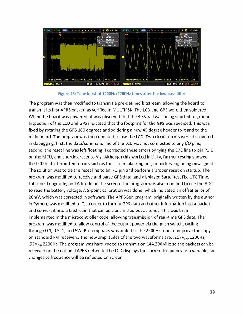
39
Figure 43: Tone burst of 1200Hz/2200Hz tones after the low pass filter
The program was then modified to transmit a pre-defined bitstream, allowing the board to
transmit its first APRS packet, as verified in MULTIPSK. The LCD and GPS were then soldered.
When the board was powered, it was observed that the 3.3V rail was being shorted to ground.
Inspection of the LCD and GPS indicated that the footprint for the GPS was reversed. This was
fixed by rotating the GPS 180 degrees and soldering a new 45 degree header to it and to the
main board. The program was then updated to use the LCD. Two circuit errors were discovered
in debugging; first, the data/command line of the LCD was not connected to any I/O pins,
second, the reset line was left floating. I corrected these errors by tying the D/C line to pin P1.1
on the MCU, and shorting reset to VCC. Although this worked initially, further testing showed
the LCD had intermittent errors such as the screen blacking out, or addressing being misaligned.
The solution was to tie the reset line to an I/O pin and perform a proper reset on startup. The
program was modified to receive and parse GPS data, and displayed Sattelites, Fix, UTC Time,
Latitude, Longitude, and Altitude on the screen. The program was also modified to use the ADC
to read the battery voltage. A 5-point calibration was done, which indicated an offset error of
20mV, which was corrected in software. The APRSGen program, originally written by the author
in Python, was modified to C, in order to format GPS data and other information into a packet
and convert it into a bitstream that can be transmitted out as tones. This was then
implemented in the microcontroller code, allowing transmission of real-time GPS data. The
program was modified to allow control of the output power via the push switch, cycling
through 0.1, 0.5, 1, and 5W. Pre-emphasis was added to the 2200Hz tone to improve the copy
on standard FM receivers. The new amplitudes of the two waveforms are: .217Vp-p 1200Hz,
.52Vp-p 2200Hz. The program was hard-coded to transmit on 144.390MHz so the packets can be
received on the national APRS network. The LCD displays the current frequency as a variable, so
changes to frequency will be reflected on screen.
40
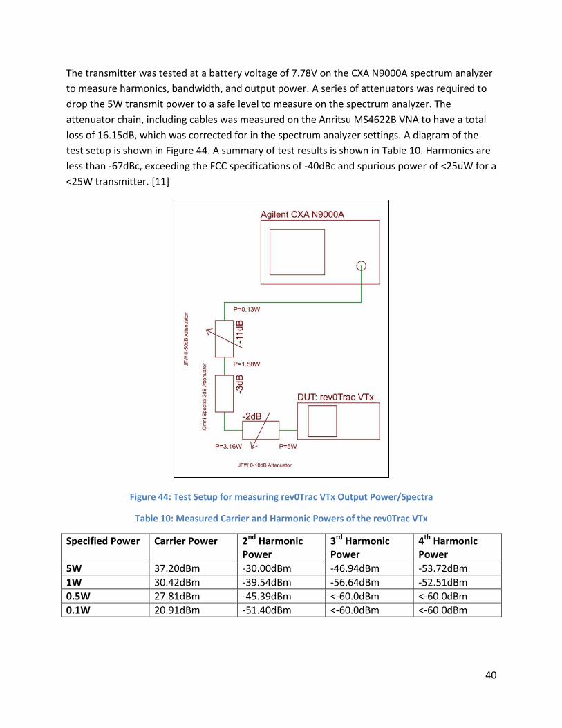
The transmitter was tested at a battery voltage of 7.78V on the CXA N9000A spectrum analyzer
to measure harmonics, bandwidth, and output power. A series of attenuators was required to
drop the 5W transmit power to a safe level to measure on the spectrum analyzer. The
attenuator chain, including cables was measured on the Anritsu MS4622B VNA to have a total
loss of 16.15dB, which was corrected for in the spectrum analyzer settings. A diagram of the
test setup is shown in Figure 44. A summary of test results is shown in Table 10. Harmonics are
less than -67dBc, exceeding the FCC specifications of -40dBc and spurious power of <25uW for a
<25W transmitter. [11]
Figure 44: Test Setup for measuring rev0Trac VTx Output Power/Spectra
Table 10: Measured Carrier and Harmonic Powers of the rev0Trac VTx
Specified Power Carrier Power 2nd Harmonic Power
3rd Harmonic Power
4th Harmonic Power
5W 37.20dBm -30.00dBm -46.94dBm -53.72dBm
1W 30.42dBm -39.54dBm -56.64dBm -52.51dBm
0.5W 27.81dBm -45.39dBm <-60.0dBm <-60.0dBm
0.1W 20.91dBm -51.40dBm <-60.0dBm <-60.0dBm

41
VI. Conclusions and Future Work
Due to time limitations, the device was only programmed to transmit a packet of a fixed type
(simple GPS position packet), and the frequency was hard-coded and requires recompiling and
updating the firmware to change. However, the framework, including hardware and software,
has been laid to upgrade to a more flexible program that would allow the user to modify packet
type and information on the device, and have the new data stored to on-board flash. The
prototyped hardware (version 1.0) contains several errors, but a revised version (1.1) has been
created, containing the changes listed in Appendix C, and an updated PCB layout is available for
future use. The revised schematic and layout can be found in Appendix B and C. The final
version 1.0 transmitter prototype is shown in Figure 45.
The completed device fulfills all stated marketing requirements and engineering specifications.
Namely, the device is self-contained and compact, transmits real-time GPS data on the APRS
network at a power greater than 5W, contains a battery that can operate the device for over 6
hours under the worst-case use conditions, and contains a user interface to display status and
allow the user to change settings.
Figure 45: Final working rev0Trac VTx APRS Transmitter

42
VII. Bibliography
[1] B. Bruninga, "APRS Articles," 14 March 1999. [Online]. Available:
http://www.aprs.org/APRS-docs/ARTICLES.TXT. [Accessed 3 June 2012].
[2] W. A. Beech, D. E. Nielsen and J. Taylor, "AX.25 Link Access Protocol for Amateur Packet
Radio," July 2008. [Online]. Available: http://www.tapr.org/pdf/AX25.2.2.pdf. [Accessed 3
June 2012].
[3] A. W. Group, "APRS Protocol Reference Version 1.0," 29 August 2000. [Online]. Available:
http://www.aprs.org/doc/APRS101.PDF. [Accessed 3 June 2012].
[4] A. Wiki, "Symbols and SSIDs," 29 May 2010. [Online]. Available:
http://info.aprs.net/index.php?title=SymbolsAndSSIDs. [Accessed 3 June 2012].
[5] J. Hansen, "PIC-et Radio: How to Send AX.25 UI Frames Using Inexpensive PIC
Microprocessors," [Online]. Available: www.tnc-x.com/dcc.doc. [Accessed 3 June 2012].
[6] F. C. Commission, "Code of Federal Regulations Title 47 Volume 5 Part 97.307: Emission
Standards," 1 October 2011. [Online]. Available: http://www.gpo.gov/fdsys/pkg/CFR-2011-
title47-vol5/xml/CFR-2011-title47-vol5-part97.xml#seqnum97.307. [Accessed 3 June
2012].
[7] Micrel Inc., "MICRF112 QwikRadio UHF ASK/FSK Transmitter," December 2011. [Online].
Available: http://www.micrel.com/_PDF/micrf112.pdf. [Accessed 5 June 2012].
[8] ETSI, "Short Range Devices," 2011. [Online]. Available:
http://www.etsi.org/website/Technologies/ShortRangeDevices.aspx. [Accessed 5 June
2012].
[9] NXP Semiconductors, "BAT754 series Schottky barrier (double) diodes," 25 March 2003.
[Online]. Available: http://www.nxp.com/documents/data_sheet/BAT754_SERIES.pdf.
[Accessed 6 June 2012].
[10] A. C. Ltd., "Frequency Modulation Bandwidth, Spectrum & Sidebands," [Online]. Available:
http://www.radio-electronics.com/info/rf-technology-design/fm-frequency-
modulation/spectrum-bandwidth-sidebands.php. [Accessed 5 June 2012].
[11] F. C. Commission, "Title 47, Part 97, Sec. 307 Emission Standards," October 2000. [Online].

43
Available: http://www.gpo.gov/fdsys/pkg/CFR-2000-title47-vol5/xml/CFR-2000-title47-
vol5-sec97-307.xml. [Accessed 5 June 2012].
[12] STMicroelectronics, "2 stages RF power amp: PD84001-E + PD54008L-E + LPF N-Channel
Enhancement-Mode Lateral MOSFETs," April 2007. [Online]. Available:
http://www.st.com/internet/evalboard/product/205439.jsp. [Accessed 5 June 2012].
[13] STMicroelectronics, "PD54008-E RF power transistor, LdmoST plastic family N-channel
enhancement-mode, lateral MOSFETs," May 2011. [Online]. Available:
http://www.st.com/internet/analog/product/133432.jsp#DATASHEET. [Accessed 5 June
2012].
[14] STMicroelectronics, "PD84001 RF power transistor the LdmoST plastic family," August
2008. [Online]. Available: http://www.st.com/internet/analog/product/138263.jsp.
[Accessed 5 June 2012].
[15] Mitsubishi Electric, "RA07M1317M 135-175MHz 6.5W 7.2V, 2 Stage Amp. For Portable
Radio," 30 June 2010. [Online]. Available: http://www.mitsubishielectric-
mesh.com/products/pdf/ra07m1317m.pdf. [Accessed 5 June 2012].
[16] R. Kollman, "Power electronics from the USB port," 2002. [Online]. Available:
http://www.ti.com/lit/an/slyt118/slyt118.pdf. [Accessed 5 June 2012].
[17] Texas Instruments Inc., "TPS61085 650 kHz/1.2 MHz, 18.5 V Step-Up DC-DC Converter,"
June 2008. [Online]. Available: http://www.ti.com/lit/ds/symlink/tps61085.pdf. [Accessed
5 June 2012].
[18] Microchip Technology Inc., "MCP73841/2/3/4 Advanced Single or Dual Cell Lithium-
Ion/Lithium-Polymer Charge Management Controllers," 2004. [Online]. Available:
http://ww1.microchip.com/downloads/en/DeviceDoc/21823c.pdf. [Accessed 5 June 2012].
[19] Texas Instruments Inc., "MSP430F550x MSP430F5510 Mixed Signal Microcontroller,"
March 2011. [Online]. Available: http://www.ti.com/lit/ds/symlink/msp430f5510.pdf.
[Accessed 5 June 2012].
[20] MediaTek Inc., "Mediatek - 3329 Datasheet," 30 April 2010. [Online]. Available:
https://docs.google.com/fileview?id=0B_dHj7E2weiiNmUzNDA3OTktNTNhNy00Y2Y5LTg0Y
TQtMzIyNzJhZmFiNjcy&hl=en. [Accessed 5 June 2012].

44
[21] "ITAR Category XV," [Online]. Available:
http://www.oria.cornell.edu/export/keywords/categoryXV.htm. [Accessed 6 June 2012].

45
A. Senior Project Analysis
Project Title: All-In-One APRS Transmitter
Student’s Name: Justin Kenny Student’s Signature:
Advisor’s Name: John Saghri Advisor’s Initials: Date:
• Summary of Functional Requirements
The Automatic Packet Reporting System (APRS) is a digital radio system that allows
transmission of data using an analog FM radio link. APRS allows position, brief messages, and
other data to be distributed across a network, independent of infrastructure, making it ideal for
applications such as search and rescue, asset management, and event tracking, while maintaining
low cost and operating even when cellular and internet services are unavailable. This project
encompasses the design, build, and test of a compact, low-cost APRS transmitter, which will
include a 5W radio, GPS, and LCD-based user interface, to allow full utilization of APRS.
• Primary Constraints
The primary constraints for this project are size, weight, and power. The system must be portable
and lightweight in order to not hinder the user or end application, and must operate for a
significant duration of time while transmitting at a high output power. Some of the difficulties of
this project include finding an amplifier that can operate at 5W output power while running from
a battery of 6-8.4V, and determining and managing a power source that is capable of the project
requirements. This project is limited by the battery in both size and operating life, and the output
power is a limitation of the chosen power amplifier.
• Economic
The economic impacts are mainly due to the procurement of parts and equipment needed to
complete the project. I provided most of the research and labor for this project, as well as
purchasing of all components and PCBs. The test equipment at Cal Poly was also used during the
course of this project. Some of the program design was done prior to the start of this project, both
from previous personal projects and from work I did at the Naval Postgraduate School. Natural
resources involved are primarily the use of electricity, which comes from the consumption of
natural resources.
Costs mostly accumulate through the prototyping and development part of the project life cycle.
Once the project is built and completed, it requires very little maintenance and costs, providing
benefit through its lifetime.

46
This project will not earn any money directly, but its use can benefit its users, by assisting in the
tracking and reporting of people, vehicles, or objects, which may alleviate the costs of other
solutions, such as a human radio operator, or cellular/internet based device.
The project has been completed on June 6, 2012, and should have an operational life of
approximately 10 years. The licensing of an operator is required for the use of the radio. The
maintenance costs are only the electricity used to charge the main battery, and the replacement of
the battery every 2 years. Once the project is completed, the user may upgrade firmware as fixes
and upgrades are released. At the end of the product lifecycle, components should be recycled
properly through electronic waste services. See Appendix E for timing details.
• If manufactured on a commercial basis:
There are no plans for commercial development of this device. The manufacturing cost of this
device is approximately $100-150 (excluding labor), and the purchase price is $200-250,
providing a profit of approximately $50-100. The cost to operate this device is approximately
$6.54/year based on a usage of 100 recharges per year, at an electricity cost of $0.171/kWh, as
well as a cost of $12.53 to replace the battery every 2 years.
• Environmental
The environmental impacts of the device are mainly from the procurement of parts and energy
usage, however serious consideration must be made to dispose of the battery safely and properly
every 2 years. Although the batteries are landfill safe, care must be taken in properly discharging
the battery and inspecting for damage before disposal. This project uses natural resources
indirectly through the use of power when charging and in operation.
• Manufacturability
The main challenge to manufacturing is the construction of the device, which will require fine-
pitch surface mount soldering. For the initial prototypes and completed project, construction was
be done by hand.

47
• Sustainability
The only maintenance this system requires once built is proper charging and storage of the
battery, which must also be replaced and properly disposed of every 2 years. If possible, this
project should use renewable energy sources for charging the battery. This project may be
improved by using better and more refined means of data transfer, as wireless technologies
improve, which would provide a faster data link for general purpose use, beyond simply
reporting GPS coordinates. Challenges in upgrading the system are mainly in programming;
however the hardware is also speed limited by the PLL bandwidth.
• Ethical
This project provides means of tracking people or vehicles, with or without their knowledge, and
the dissemination of this information across the APRS network, including internet servers. The
intended application for this project would be for tracking vehicles or people at events, or
tracking autonomous vehicles, which would benefit the users of the device. The ethical use of the
device requires that all parties involved in tracking are aware of the device and its capabilities.
• Health and Safety
The only health and safety concerns are in the construction and manufacture of the project. Care
will be taken to use lead-free solder and RoHS compliant components in its manufacture,
however some components or systems used may not meet this requirement, and there are dangers
involved in soldering and construction of the product. In use, there are little health and safety
concerns, but the charging process must be monitored and done in a safe location to ensure the
battery or device does not become damaged.
• Social and Political
There are social and political issues involved with the ethical use of this project. As mentioned
previously, it can be used to track many objects, which may lead to its misuse if those being
tracked are unaware of the device. It is up to the end user to use this device in an ethical and safe
manner. The stakeholders are the users or organizations that will use this project. The
stakeholders would benefit equally from the proper use of this project, and this project does not
directly cause any inequities.

48
• Development
The development of this project involves research of new components to meet the project
requirements, including battery, power amplifier, RF IC, and supporting circuitry. This project
involved the use of the vector network analyzer, spectrum analyzer, and simulation software to
analyze the amplifier and filter, as well as software tools and calculations for the RF IC and
power management circuitry.

49
B. Schematic
Figure 46: Revised rev0Trac VTx Schematic

50
C. PCB Layout
Figure 47: Revised rev0Trac VTx PCB Layout
List of Changes in version 1.1:
Added trace from MCU to LCD RST line
Added trace from MCU to LCD D/C line
Added trace from MCU to LCD backlight PMOS
Added 1k resistor to ground on VUSBR line
Added tri-state buffer and header to accommodate an external GPS or serial UART
connection

51
D. Bill of Materials
Table 11: Bill of Materials for rev0Trac VTx Version 1.1
Item # Qty Reference Designator Type Value Package Manufacturer Manufacturer Part # Digi-Key Part # Unit Price Subtotal
1 2 C39, C41 Ceramic Capacitor 5.1pF, C0G 50V, ±0.25pF 0603 Standard 0.01$ 0.02$
2 2 C13, C14 Ceramic Capacitor 22pF, C0G 50V, ±5% 0603 Standard 0.01$ 0.02$
3 2 C35, C37 Ceramic Capacitor 36p, C0G 50V, ±5% 0805 Standard 0.01$ 0.02$
4 1 C36 Ceramic Capacitor 56p, C0G 50V, ±5% 0805 Standard 0.01$ 0.01$
5 1 C28 Ceramic Capacitor 1n, X7R 50V, ±10% 0603 Standard 0.01$ 0.01$
6 1 C26 Ceramic Capacitor 1.1n, X7R 50V, ±10% 0603 Standard 0.12$ 0.12$
7 1 C32 Ceramic Capacitor 1.2n, X7R 50V, ±10% 0603 Standard 0.07$ 0.07$
8 1 C11 Ceramic Capacitor 2.2n, X7R 50V, ±10% 0603 Standard 0.01$ 0.01$
9 1 C33 Ceramic Capacitor 2.7n, X7R 50V, ±10% 0603 Standard 0.08$ 0.08$
10 2 C16, C17 Ceramic Capacitor 4.7n, X7R 50V, ±10% 0603 Standard 0.01$ 0.02$
11 2 C6, C42 Ceramic Capacitor 10n, X7R 25V, ±10% 0603 Standard 0.01$ 0.02$
12 1 C1 Ceramic Capacitor 15n, X7R 25V, ±10% 0603 Standard 0.01$ 0.01$
13 1 C38 Ceramic Capacitor 22n, X7R 25V, ±10% 0603 Standard 0.01$ 0.01$
14 1 C31 Ceramic Capacitor 47n, X7R 25V, ±10% 0603 Standard 0.01$ 0.01$
15 11
C15, C18, C20, C21, C23,
C25, C34, C40 C45, C46, C58 Ceramic Capacitor 100n, X7R 25V, ±10% 0603 Standard 0.01$ 0.11$
16 2 C8, C10 Ceramic Capacitor 220n, X7R 16V, ±10% 0603 Standard 0.01$ 0.02$
17 2 C3, C30 Ceramic Capacitor 470n, X5R 10V, ±10% 0603 Standard 0.01$ 0.02$
18 1 C29 Ceramic Capacitor 2.2u, X5R 10V, ±10% 0603 Standard 0.01$ 0.01$
19 2 C2, C5 Ceramic Capacitor 4.7u, X5R 10V, ±10% 0603 Kemet C0603C475K8PACTU 399-5503-1-ND 0.23$ 0.47$
20 3 C19, C22, C24 Tantalum Capacitor 10u, 16V, ±20%, 3Ω 1206 Vishay 293D106X0016A2TE3 0.07$ 0.21$
21 5 C27, C43, C44, C54, C55 Ceramic Capacitor 10uF, X5R 10V, ±10% 0805 Yaego CC0805KKX5R6BB106 311-1460-1-ND 0.13$ 0.65$
22 2 C4, C12 Tantalum Capacitor 22u, 16V, ±10%, 1.9Ω 3528 Vishay 293D226X9016B2TE3 718-1138-1-ND 0.91$ 1.82$
23 1 R20 Resistor 0.5 0603 Standard 0.00$ 0.00$
24 2 R1, R2 Resistor 27 0603 Standard 0.00$ 0.01$
25 5 R8, R12, R13, R21, R22 Resistor 100 0603 Standard 0.00$ 0.01$
26 2 R5, R35 Resistor 330 0603 Standard 0.00$ 0.01$
27 1 R15 Resistor 360 0603 Standard 0.00$ 0.00$
28 5 R10, R11, R16, R23, R24 Resistor 1k 0603 Standard 0.00$ 0.01$
29 1 R18 Resistor 1.2k 0603 Standard 0.00$ 0.00$
30 1 R6 Resistor 1.4k 0603 Yaego RC0603FR-071K4L 311-1.40KHRCT-ND 0.01$ 0.01$
31 1 R19 Resistor 2k 0603 Standard 0.00$ 0.00$
32 1 R31 Resistor 3k 0603 Yaego RC0603FR-073KL 311-3.00KHRCT-ND 0.01$ 0.01$
33 1 R14 Resistor 3.6k 0603 Standard 0.00$ 0.00$
34 1 R17 Resistor 7.5k 0603 Standard 0.00$ 0.00$
35 1 R4 Resistor 10k 0603 Standard 0.00$ 0.00$
36 1 R30 Resistor 12k 0603 Yaego RC0603FR-0712KL 311-12.0KHRCT-ND 0.01$ 0.01$
37 1 R9 Resistor 30k 0603 Standard 0.00$ 0.00$
38 1 R3 Resistor 47k 0603 Standard 0.00$ 0.00$
39 1 R7 Resistor 1M 0603 Standard 0.00$ 0.00$
40 1 L5 Chip Inductor 10n 0603 Taiyo Yuden HK160810NJ-T 587-1545-1-ND 0.06$ 0.06$
41 2 L8, L9 Air Core Inductor 56n 1812SMS Coilcraft 1812SMS-56NJLB 0.95$ 1.90$
42 1 L6 Chip Inductor 470n 0603 Taiyo Yuden HK1608R47J-T 587-1565-1-ND 0.06$ 0.06$
43 1 L4 Power Inductor 3.3u SMD 3mm Bourns SRN3015-3R3M SRN3015-3R3MCT-ND 0.33$ 0.33$
44 2 F1, F2 PTC Resettable Fuse 1.50A 1812 Bel Fuse 0ZCC0150FF2C 507-1503-1-ND 0.33$ 0.66$
45 3 D1, D3, D4 Schottky Diode PMEG3020ER SOD123W NXP PMEG3020ER,115 568-6518-1-ND 0.48$ 1.44$
46 1 LED1 LED STAT 0603 Standard 0.27$ 0.27$
47 1 LED2 LED PWR 0603 Standard 0.11$ 0.11$
48 1 LED3 LED GRN 0603 Standard 0.10$ 0.10$
49 1 Q1 N-Channel MOSFET 2N7002P SOT-23 NXP 2N7002P,215 568-5818-1-ND 0.12$ 0.12$
50 1 Q4 P-Channel MOSFET FDS6673BZ SOIC-8 Fairchild FDS6673BZ FDS6673BZCT-ND 1.28$ 1.28$
51 1 Q5 P-Channel MOSFET DMG1013T SOT-323 Diodes Inc DMG1013T-7 DMG1013T-7DICT-ND 0.20$ 0.20$
52 1 U1 Microcontroller IC MSP430F5508 TQFP-48 TI MSP430F5508IPT 296-29602-5-ND 4.13$ 4.13$
53 1 U2 RF Power Amplifier IC RA07M1317M RA07M1317M Mitsubishi RA07M1317M 19.95$ 19.95$
54 1 U3 LiPo Charger IC MCP73844 MSOP-8 Microchip MCP73844-840I/MS MCP73844-840I/MS-ND 1.56$ 1.56$
55 1 U4 Boost Converter IC TPS61085 MSOP-8 TI TPS61085DGKT 296-23550-1-ND 3.17$ 3.17$
56 1 U5 LiPo Balancer IC BQ29209 SON-8 TI BQ29209DRBR 296-27677-1-ND 1.08$ 1.08$
57 1 U6 RF Transmitter IC ADF7012 TSSOP-24 Analog Devices ADF7012BRUZ ADF7012BRUZ-ND 4.26$ 4.26$
58 2 U7, U12 DAC IC DACX311 SOT-363 TI DAC7311IDCKR 296-23717-1-ND 2.73$ 5.46$
59 1 U8 Voltage Reference IC LM4040 SOT-23 TI LM4040A20IDBZR 296-20857-1-ND 2.88$ 2.88$
60 2 U9, U10 Voltage Regulator IC TLV1117 TO-261 TI TLV1117-33CDCYR 296-21112-1-ND 0.66$ 1.32$
61 1 U11 Dual Tri-State Buffer IC SN74LVC2G241 8-VFSOP TI SN74LVC2G241DCUR 296-11936-1-ND 0.28$ 0.28$
62 1 GPS GPS Module FGPMMOPA6B SMD GlobalTop FGPMMOPA6B 29.99$ 29.99$
63 1 LCD Graphic LCD GRAPHIC_LCD GRAPHIC_LCD 4.95$ 4.95$
64 1 X1 VCXO VCXO_ASVV VCXO_ASVV Abracon ASVV-20.000MHZ-N152-T 535-9344-1-ND 3.63$ 3.63$
65 1 X2 Crystal SMD 5x3.2mm Abracon ABM3-24.000MHZ-B2-T 535-9106-1-ND 1.43$ 1.43$
66 1 J1 Female SMA Connector SMA F SMA F Standard 0.50$ 0.50$
67 1 J2 JST-SB3 Connector BATT JST-SB3 JST 455-2250-ND 0.21$ 0.21$
68 1 JP2 Male Header 0.1" GPS M06 Standard 0.06$ 0.06$
69 1 J3 Male Header 0.1" GPS M04 Standard 0.04$ 0.04$
70 1 CON1 Micro USB Connector USBMICRO_B_FCI USBMICRO_B FCI 10118193-0001LF 609-4616-1-ND 0.87$ 0.87$
71 1 S1 Tactile Switch Rt. Angle SW SWITCH-MOM-RT E-Switch TL3330AF260QG EG4389CT-ND 0.53$ 0.53$
72 1 S2 Tactile Switch PUR TAC_SWITCHSMD Standard 0.12$ 0.12$
73 1 SW1 Slide Switch PWR SLIDE_SW_9.5MM Standard 0.25$ 0.25$
74 1 SW2 Rotary Encoder ENCODER ENCODER Panasonic EVQ-WKA001 P13381SCT-ND 6.11$ 6.11$
75 2 BATT LiPo Battery 2200mAH 3.7V BATT HobbyKing 3.61$ 7.22$
76 1 HS Heatsink 28x28mm Wakefield 345-1097-ND 658-45ABT3 2.44$ 2.44$
77 1 J2F JST-SB3 Female Conn. JST-XHP-3 JST XHP-3 455-2219-ND 0.10$ 0.10$
78 3 J2P JST-Crimp Pins SXH JST SXH-001T-P0.6 455-1135-1-ND 0.04$ 0.11$
79 1 GPS-PCB Printed Circuit Board GPS-PCB 0.8x0.65" OSH Park 0.87$ 0.87$
80 1 PCB Printed Circuit Board PCB 3.8x1.8" Imagineering 25.00$ 25.00$
138.90$ Total Cost

52
E. Schedule – Time Estimates
9/16 10/7 10/28 11/18 12/9 12/30 1/20 2/10 3/2 3/23 4/13 5/4 5/25
Abstract (Proposal)
Requirements and Specs
Block Diagram
Literature Search
Gantt Chart
Cost Estimates
ABET Analysis
Requirements and Specs v2
Report
Report v2
Finalize Requirements
APRS Transmitter Prototype
Order Parts/PCBs
Build
Program
Debug/Test
Final APRS Transmitter
Order Parts/PCB
Build
Program
Debug/Test
Interim Final Report
Final Report
Intro
Background
Technical
Results/Appendices
Task Description Start Date End Date Duration
Abstract (Proposal) 9/16/2011 9/18/2011 2
Requirements and Specs 9/21/2011 9/30/2011 9
Block Diagram 10/5/2011 10/9/2011 4
Literature Search 9/21/2011 10/10/2011 19
Gantt Chart 10/19/2011 10/23/2011 4
Cost Estimates 10/19/2011 10/23/2011 4
ABET Analysis 10/26/2011 10/30/2011 4
Requirements and Specs v2 11/2/2011 11/6/2011 4
Report 9/19/2011 10/30/2011 41
Report v2 11/21/2011 12/2/2011 11
Finalize Requirements 12/5/2011 12/19/2011 14
APRS Transmitter Prototype 1/9/2012 3/12/2012 63
Order Parts/PCBs 1/9/2012 1/30/2012 21
Build 1/30/2012 2/13/2012 14
Program 2/13/2012 3/4/2012 20
Debug/Test 2/25/2012 3/12/2012 16
Final APRS Transmitter 3/12/2012 5/15/2012 64
Order Parts/PCB 3/12/2012 4/1/2012 20
Build 4/1/2012 4/11/2012 10
Program 4/11/2012 5/2/2012 21
Debug/Test 5/2/2012 5/15/2012 13
Interim Final Report 1/2/2012 3/2/2012 60
Final Report 3/26/2012 6/1/2012 67
Intro 1/2/2012 1/11/2012 9
Background 1/11/2012 2/8/2012 28
Technical 2/8/2012 4/18/2012 70
Results/Appendices 4/18/2012 6/1/2012 44
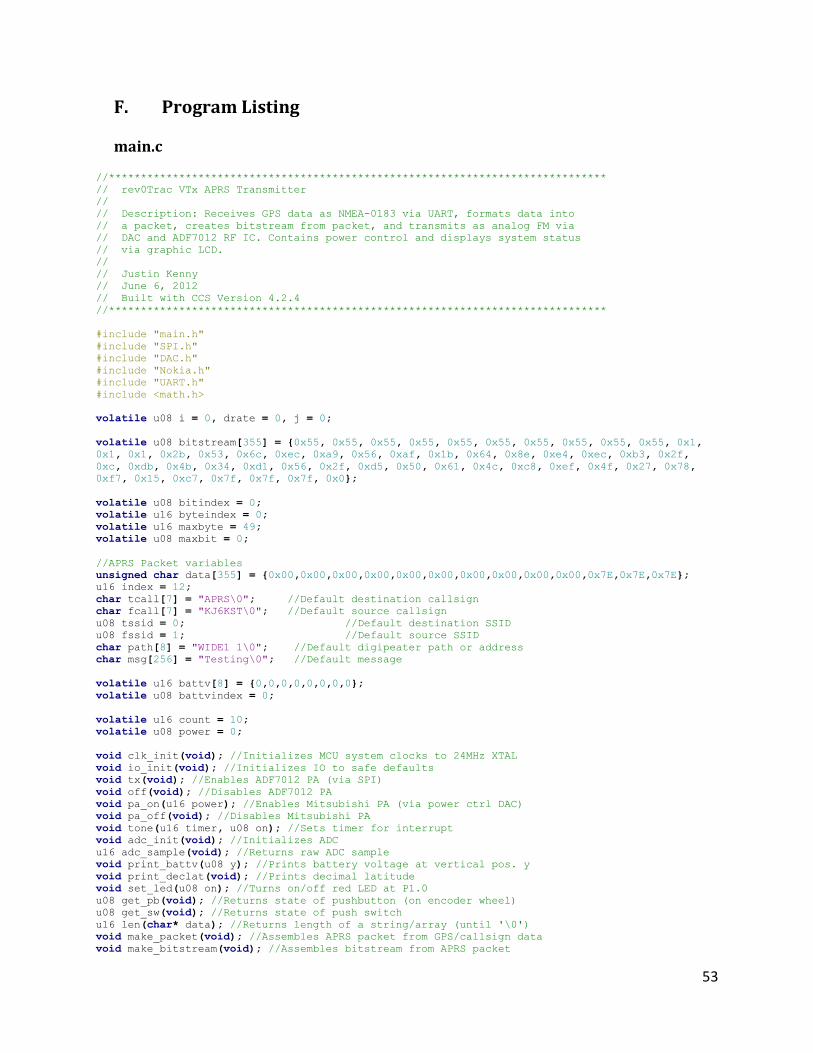
53
F. Program Listing
main.c
//******************************************************************************
// rev0Trac VTx APRS Transmitter
//
// Description: Receives GPS data as NMEA-0183 via UART, formats data into
// a packet, creates bitstream from packet, and transmits as analog FM via
// DAC and ADF7012 RF IC. Contains power control and displays system status
// via graphic LCD.
//
// Justin Kenny
// June 6, 2012
// Built with CCS Version 4.2.4
//******************************************************************************
#include "main.h"
#include "SPI.h"
#include "DAC.h"
#include "Nokia.h"
#include "UART.h"
#include <math.h>
volatile u08 i = 0, drate = 0, j = 0;
volatile u08 bitstream[355] = 0x55, 0x55, 0x55, 0x55, 0x55, 0x55, 0x55, 0x55, 0x55, 0x55, 0x1,
0x1, 0x1, 0x2b, 0x53, 0x6c, 0xec, 0xa9, 0x56, 0xaf, 0x1b, 0x64, 0x8e, 0xe4, 0xec, 0xb3, 0x2f,
0xc, 0xdb, 0x4b, 0x34, 0xd1, 0x56, 0x2f, 0xd5, 0x50, 0x61, 0x4c, 0xc8, 0xef, 0x4f, 0x27, 0x78,
0xf7, 0x15, 0xc7, 0x7f, 0x7f, 0x7f, 0x0;
volatile u08 bitindex = 0;
volatile u16 byteindex = 0;
volatile u16 maxbyte = 49;
volatile u08 maxbit = 0;
//APRS Packet variables
unsigned char data[355] = 0x00,0x00,0x00,0x00,0x00,0x00,0x00,0x00,0x00,0x00,0x7E,0x7E,0x7E;
u16 index = 12;
char tcall[7] = "APRS\0"; //Default destination callsign
char fcall[7] = "KJ6KST\0"; //Default source callsign
u08 tssid = 0; //Default destination SSID
u08 fssid = 1; //Default source SSID
char path[8] = "WIDE1 1\0"; //Default digipeater path or address
char msg[256] = "Testing\0"; //Default message
volatile u16 battv[8] = 0,0,0,0,0,0,0,0;
volatile u08 battvindex = 0;
volatile u16 count = 10;
volatile u08 power = 0;
void clk_init(void); //Initializes MCU system clocks to 24MHz XTAL
void io_init(void); //Initializes IO to safe defaults
void tx(void); //Enables ADF7012 PA (via SPI)
void off(void); //Disables ADF7012 PA
void pa_on(u16 power); //Enables Mitsubishi PA (via power ctrl DAC)
void pa_off(void); //Disables Mitsubishi PA
void tone(u16 timer, u08 on); //Sets timer for interrupt
void adc_init(void); //Initializes ADC
u16 adc_sample(void); //Returns raw ADC sample
void print_battv(u08 y); //Prints battery voltage at vertical pos. y
void print_declat(void); //Prints decimal latitude
void set_led(u08 on); //Turns on/off red LED at P1.0
u08 get_pb(void); //Returns state of pushbutton (on encoder wheel)
u08 get_sw(void); //Returns state of push switch
u16 len(char* data); //Returns length of a string/array (until '\0')
void make_packet(void); //Assembles APRS packet from GPS/callsign data
void make_bitstream(void); //Assembles bitstream from APRS packet

54
void main(void)
WDTCTL = WDTPW + WDTHOLD; //Stop watchdog timer
clk_init();
/* Main Program Begin */
io_init();
spi_init();
pa_off();
uart_init();
adc_init();
nlcd_init();
nlcd_clear();
float freq = 0;
u16 freqint = 0;
u16 freqdec = 0;
u16 frac = 1199;
u08 integer = 108;
u08 i = 0;
u08 j = 0;
char temp[21] = 0,0,0,0,0,0,0,0,0,0,0,0,0,0,0,0,0,0,0,0,0;
char chr[5];
spi_out32(0x0415,0xE000); //R0 Set
_delay_us(100);
spi_out24(0x40|(integer>>2),0x0001|(integer<<14)|(frac<<2)); //R1 Set
_delay_us(100);
spi_out32(0x0000,(0x802A|(16<<5))); //R2 Set
_delay_us(100);
spi_out32(0x004A,0x2037); //R3 Set
//tx();
TA0CTL = (2<<8) | (1<<4); //Set TA0 using SMCLK, in Up mode
TA1CTL = (2<<8) | (1<<4); //Set TA1 using SMCLK, in Up mode
TA1CCR0 = 20000; //1200 baud interrupt
_BIS_SR(GIE); //Global interrupt enable
tone(1250,0);
s16 num = 0;
u08 flag = 0;
while(1)
if(count > 15 || count < 7)
nlcd_clear();
nlcd_string(0,0,"Sats:");
nlcd_string(36,0,"Fix:");
nlcd_string(0,8,"UTC:");
nlcd_string(0,16,"Lat:");
nlcd_string(0,24,"Lng:");
nlcd_chr5(56,0,gpsdata.valid); //Valid flag
nlcd_string(24,0,gpsdata.sats); //Sattelites in view
for(j=0;j<6;j++)
temp[j] = gpsdata.time[j];
temp[j] = '\0';
nlcd_string(20,8,temp); //UTC Time
for(j=0;j<9;j++)
temp[j] = gpsdata.lat[j];
temp[j++] = gpsdata.ns;
temp[j] = '\0';
nlcd_string(20,16,temp); //Latitude
for(j=0;j<10;j++)

55
temp[j] = gpsdata.lng[j];
temp[j++] = gpsdata.ew;
temp[j] = '\0';
nlcd_string(20,24,temp); //Longitude
/* Frequency Display */
nlcd_string(36,40,"Frq:");
freq = 20.0/15.0*(integer+(frac)/4096.0);
//Integer Part
freqint = (u16)freq;
chr[2] = (freqint/100)%10+0x30;
chr[1] = (freqint/10)%10+0x30;
chr[0] = freqint%10+0x30;
for(j=0,i=3;i>0;i--,j++)
nlcd_chr5(56+(j<<2),40,chr[(i-1)]);
//Decimal Part
freqdec = (u16)((freq - (u16)freq)*1000);
nlcd_chr5(68,40,'.');
chr[2] = (freqdec/100)%10+0x30;
chr[1] = (freqdec/10)%10+0x30;
chr[0] = freqdec%10+0x30;
for(j=0,i=3;i>0;i--,j++)
nlcd_chr5(72+(j<<2),40,chr[(i-1)]);
/* End Frequency Display */
if(get_pb())
count = 0;
if(get_sw())
power = (power==4) ? 0 : power+1;
print_battv(32);
nlcd_string(0,40,"Pwr: ");
if(power == 0)
nlcd_string(20,40,".1W");
else if(power == 1)
nlcd_string(20,40,".5W");
else if(power == 2)
nlcd_string(20,40,"1W ");
else
nlcd_string(20,40,"5W ");
if(count == 0)
bitindex = 0;
byteindex = 0;
UCA1IE = 0; //Disable receive interrupt
make_packet();
make_bitstream();
if(power == 0)
pa_on(LOW);
else if(power == 1)
pa_on(MED);
else if(power == 2)
pa_on(HI1);
else
pa_on(HI2);
tx();
else if(count == 7)
TA1CCTL0 = (1<<4); //Enable CCR0 interrupt
56
else if(count == 30)
pa_off();
off();
count = (count==1800) ? 0 : count+1;
_delay_ms(100);
void clk_init(void)
/* Initialize Clocks */
UCSCTL6 = (3<<14)|(1); //XT2 16MHz, XT1 Off
UCSCTL3 |= (2<<4); //FLL uses REFO
UCSCTL4 = (2<<8)|(3<<4)|(3); //ACLK = REFOCLK, SMCLK = DCOCLK, MCLK = DCOCLK
sbi(P5SEL,2);
do
UCSCTL7 &= ~(XT2OFFG + XT1LFOFFG + DCOFFG); // Clear XT2,XT1,DCO fault flags
SFRIFG1 &= ~OFIFG; // Clear fault flags
_delay_us(1);
while (SFRIFG1 & OFIFG); // Test oscillator fault flag
UCSCTL4 = (5<<8)|(5<<4)|(5); //ACLK = XT2, SMCLK = XT2, MCLK = XT2
/* End Clock Initialization */
void io_init(void)
//Check IO Map in main.h for Details
//Port 1 Init
P1DIR = 0xEB;
sbi(P1OUT,3); //Set RST on LCD
sbi(P1REN,4); //Pullup on Switch In
sbi(P1OUT,4);
sbi(P1OUT,5); //Deselect FM DAC
sbi(P1OUT,6); //Deselect LCD
//Port J Init (JTAG as IO)
PJDIR = 0x04;
sbi(PJOUT,2); //Enable GPS
sbi(PJREN,3); //Pullup on Rotary Switch PB In
sbi(PJOUT,3);
//Port 4 Init
P4DIR = 0xDA;
sbi(P4REN,0); //Pullup on Rotary Switch A In
sbi(P4OUT,0);
sbi(P4REN,2); //Pullup on Rotary Switch B In
sbi(P4OUT,2);
sbi(P4OUT,6); //Deselect Gate DAC
sbi(P4OUT,7); //Deselect ADF
//Port 5 Init
sbi(P5SEL,0); //Select VeREF+
sbi(P5SEL,1); //Select VeREF-
//Port 6 Init
P6SEL = 0x08; //Select ADC Input
void set_led(u08 on)
if(on)
sbi(P1OUT,0);
else
cbi(P1OUT,0);

57
u08 get_pb(void)
return !(PJIN & 0x08);
u08 get_sw(void)
return !(P1IN & 0x10);
void tone(u16 timer, u08 on)
if(on)
TA0CCR0 = timer; //Default to 1200*16 Hz
TA0CCTL0 = (1<<4); //Enable CCR0 interrupt
else
wdac_direct(31,252);
TA0CCTL0 = 0; //Disable CCR0 interrupt
void tx(void)
spi_out32(0x0045,0x20FF); //PA On
void off(void)
spi_out32(0x004A,0x2037); //PA Off
void pa_on(u16 power)
set_led(1);
dac_out(power,PDAC,PD0); //5.0ms to turn on
void pa_off(void)
dac_out(0,PDAC,PD0); //1.8ms to turn off
set_led(0);
void adc_init(void)
ADC10CTL0 = ADC10ON; //Turn on ADC10_A
ADC10CTL1 = ADC10DIV_6|ADC10SSEL_1|ADC10SHP; //Select ACLK/6 for ADCCLK
ADC10MCTL0 = ADC10SREF_6; //Select VeREF+ (Buffered) and VeREF- as refs
u16 adc_sample(void)
ADC10CTL0 = ADC10ON; //Turn on ADC10_A
ADC10MCTL0 = ADC10SREF_6|3; //Select channel 3
ADC10CTL0 |= ADC10ENC; //Enable conversions
ADC10CTL0 |= ADC10SC; //Start conversion
while(ADC10CTL1 & ADC10BUSY);
return ADC10MEM0;
void print_battv(u08 y)
float temp = 0; //Intermediate result
u08 iresult = 0; //Integer voltage

58
u08 fresult = 0; //Fractional voltage
battv[battvindex] = adc_sample();
for(;iresult<8;iresult++)
temp += battv[iresult];
temp = temp/8192.0*10.24+0.02;
if(temp<0)
temp = 0;
iresult = (int)temp;
fresult = (int)((temp - iresult)*100);
nlcd_string(0,y,"Bat:");
nlcd_chr5(24,y,'.');
nlcd_s16(20,y,iresult);
if(fresult<10)
nlcd_string(28,y,"0");
nlcd_s16(32,y,fresult);
else
nlcd_s16(28,y,fresult);
battvindex = (battvindex==7) ? 0 : battvindex+1;
u16 len(char* data)
u16 i = 0;
while(data[i]!='\0')
i++;
return i;
void make_packet(void)
u16 i;
u16 temp = 0;
index = 12;
//Select destination callsign
temp = len(tcall);
for(i=0; i<temp; i++)
//Print left-shifted tocall
data[++index] = (tcall[i]<<1);
for(i=0; i<(6-temp); i++)
//Print left-shifted spaces
data[++index] = 0x40;
//Print tocall SSID
data[++index] = (0xE0+(tssid<<1));
//Select source callsign
temp = len(fcall);
for(i=0; i<temp; i++)
//Print left-shifted tocall
data[++index] = (fcall[i]<<1);
for(i=0; i<(6-temp); i++)

59
//Print left-shifted spaces
data[++index] = 0x40;
//Print tocall SSID
data[++index] = (0xE0+(fssid<<1));
//Select path
temp = len(path);
for(i=0; i<temp; i++)
//Print left-shifted path
if(i==6)
data[++index] = (0xE1 | path[i]<<1);
else
data[++index] = (path[i]<<1);
for(i=0; i<(7-temp); i++)
//Print left-shifted spaces
data[++index] = 0x40; //Need to add condition for 0xE1 | 0x40
//Append Control Field and Protocol ID Bytes
data[++index] = 0x03;
data[++index] = 0xF0;
//Generate GPS Message
msg[0] = '!';
for(i=0; i<7; i++)
msg[i+1] = gpsdata.lat[i];
msg[8] = gpsdata.ns;
msg[9] = '/';
for(i=0; i<8; i++)
msg[i+10] = gpsdata.lng[i];
msg[18] = gpsdata.ew;
msg[19] = '>';
msg[20] = 'P';
msg[21] = 0x30+power;
msg[22] = ' ';
msg[23] = 'F';
if(gpsdata.valid=='0')
msg[24] = '0';
else
msg[24] = '1';
msg[25] = ' ';
msg[26] = 'r';
msg[27] = 'e';
msg[28] = 'v';
msg[29] = '0';
msg[30] = 'T';
msg[31] = 'r';
msg[32] = 'a';
msg[33] = 'c';
msg[34] = ' ';
msg[35] = 'V';
msg[36] = 'T';
msg[37] = 'x';
msg[38] = '\0';
//Append Message
temp = len(msg);
for(i=0; i<temp; i++)
data[++index] = msg[i];
data[++index] = 0xFF;
data[++index] = 0xFF;
data[++index] = 0x7E;
data[++index] = 0x7E;
data[++index] = 0x7E;

60
void make_bitstream(void)
u16 i;
u08 j, last = 1, onecount = 0;
u16 fcs = 0xFFFF;
u08 shiftbit = 0;
u16 bi = 0, bj = 0;
for(i=0;i<=index;i++)
if(i==(index-4))
fcs ^= 0xFFFF;
data[(index-3)] = ((fcs >> 8) & 0x00FF);
data[(index-4)] = (fcs & 0x00FF);
for(j=0;j<8;j++)
if(data[i]>>j & 0x01)
if(last)
bitstream[bi] |= (1<<(7-bj));
else
bitstream[bi] &= ~(1<<(7-bj));
bj++;
if(bj==8)
bj = 0;
bi++;
onecount++;
if(i < 13 || i > (index-3))
onecount = 0;
if(onecount == 5)
if(last)
bitstream[bi] &= ~(1<<(7-bj));
last = 0;
else
bitstream[bi] |= (1<<(7-bj));
last = 1;
onecount = 0;
bj++;
if(bj==8)
bj = 0;
bi++;
else
if(last)
bitstream[bi] &= ~(1<<(7-bj));
last = 0;
else
bitstream[bi] |= (1<<(7-bj));
last = 1;
onecount = 0;
bj++;
if(bj==8)

61
bj = 0;
bi++;
if((i < (index-4)) && (i > 12))
//Store bit rotated off in variable shiftbit
shiftbit = 0x0001 & fcs;
fcs = fcs >> 1; //Shift fcs right by 1
//If shiftbit doesn't match data being sent, xor with 0x8408
if(shiftbit != ((data[i]>>j) & 0x01))
fcs ^= 0x8408;
maxbyte = bi;
maxbit = bj;
#pragma vector=TIMER0_A0_VECTOR
__interrupt void Timer0_A0 (void)
if(drate == 0)
wdac_direct(wdac_msb[i], wdac_lsb[i]);
i = (i>=15) ? 0 : i+1;
else
wdac_direct(wdachf_msb[i], wdachf_lsb[i]);
if(i%2)
i++;
i = (i>=14) ? 0 : i+2;
#pragma vector=TIMER1_A0_VECTOR
__interrupt void Timer1_A0 (void)
if(bitstream[byteindex] & (1<<(7-bitindex))) //Next bit 1?
drate = 0;
tone(1250,1);
else //Next bit 0
drate = 1;
tone(1364,1);
bitindex++;
if(byteindex >= maxbyte)
if(bitindex >= maxbit) //Transmission complete
TA1CCTL0 = 0; //Disable CCR0 interrupt
tone(1250,0);
_delay_ms(350);
off();
pa_off();
UCA1IE = UCRXIE; //Enable receive interrupt
if(bitindex>7)
bitindex = 0;
byteindex++;
62
main.h
#ifndef MAIN_H_
#define MAIN_H_
#include <msp430f5508.h>
#define F_CPU 24000000
#define sbi(a, b) ((a) |= 1 << (b)) //sets bit B in variable A
#define cbi(a, b) ((a) &= ~(1 << (b))) //clears bit B in variable A
#define tbi(a, b) ((a) ^= 1 << (b)) //toggles bit B in variable A
#define _delay_ms(x) (_delay_cycles((F_CPU/1000)*x))
#define _delay_us(x) (_delay_cycles((F_CPU/1000000)*x))
typedef unsigned char u08;
typedef signed char s08;
typedef short unsigned int u16;
typedef short signed int s16;
typedef volatile unsigned char vu08;
typedef volatile signed char vs08;
typedef volatile unsigned short int vu16;
typedef volatile signed short int vs16;
/* IO Map
* P1.0 Status LED Out
* P1.1 LCD Data/Command Out
* P1.4 Switch In (Pullup)
* P1.5 /FM DAC Sync Out
* P1.6 /LCD Chip Select Out
* P1.7 ADF Data Out
* PJ.0 ADF Clock In
* PJ.2 GPS Enable Out
* PJ.3 Rotary Switch PB In (Pullup)
* P4.0 Rotary Switch A In (Pullup)
* P4.1 MOSI Out
* P4.2 Rotary Switch B In (Pullup)
* P4.3 SCK Out
* P4.4 RX Out
* P4.5 TX In
* P4.6 /Gate DAC Sync Out
* P4.7 /ADF Chip Select Out
* P5.0 2.048V Ref In
* P5.1 0V Ref In
* P5.2 XT2 In
* P5.3 XT2 Out
* P6.3 10.24V Sense In
* */
//Calibrated at 7.78V
//Do not exceed 3000
#define LOW 2240 //100mW
#define MED 2365 //500mW
#define HI1 2450 //1W
#define HI2 2780 //5W
#define PI 3.141593
#define D2R 0.0174533 //Multiply by D2R to convert decimal to radian
#define R2D 57.2958 //Multiply by R2D to convert radian to decimal
#define MER 3956.6 //Mean Earth radius in miles
#endif /*MAIN_H_*/

63
SPI.c
#include "SPI.h"
void spi_init(void)
//1) Set UCSWRST
UCB1CTL1 |= 1; //UCSWRST = 1
//2) Initialize all USCI registers with UCSWRST=1 (including UCxCTL1)
UCB1CTL1 = (2<<6)|1; //BRCLK = SMCLK, UCSWRST = 1
//Set CLK polarity/phase, MSB first, master mode, 3-pin mode, synchronous
UCB1CTL0 = (CLKPHS<<7)|(CLKPOL<<6)|(1<<5)|(0<<4)|(1<<3)|(0<<1)|1;
//Set clock prescalar value
UCB1BR0 = BR;
//3) Configure ports
P4SEL |= PIN_MOSI | PIN_SCLK;
//4) Clear UCSWRST via software
UCB1CTL1 &= ~(1); //UCSWRST = 0
void spi_out(u08 byte)
P4OUT &= ~(PIN_SS);
UCB1TXBUF = byte;
while(UCB1STAT & 0x01); //Wait until USCI not busy
_delay_us(1);
P4OUT |= PIN_SS;
void spi_out24(u08 msb, u16 lsb)
P4OUT &= ~(PIN_SS);
UCB1TXBUF = msb;
while(UCB1STAT & 0x01); //Wait until USCI not busy
UCB1TXBUF = ((lsb>>8) & 0xFF);
while(UCB1STAT & 0x01); //Wait until USCI not busy
UCB1TXBUF = (lsb & 0xFF);
while(UCB1STAT & 0x01); //Wait until USCI not busy
_delay_us(1);
P4OUT |= PIN_SS;
void spi_out32(u16 msb, u16 lsb)
P4OUT &= ~(PIN_SS);
UCB1TXBUF = ((msb>>8) & 0xFF);
while(UCB1STAT & 0x01); //Wait until USCI not busy
UCB1TXBUF = (msb & 0xFF);
while(UCB1STAT & 0x01); //Wait until USCI not busy
UCB1TXBUF = ((lsb>>8) & 0xFF);
while(UCB1STAT & 0x01); //Wait until USCI not busy
UCB1TXBUF = (lsb & 0xFF);
while(UCB1STAT & 0x01); //Wait until USCI not busy
_delay_us(1);
P4OUT |= PIN_SS;
64
SPI.h
/* Application generic SPI driver; must be used in conjunction
* with user written device driver containing SPI write functions */
#ifndef SPI_H_
#define SPI_H_
#include "main.h"
#define PIN_MISO 0x04 //SPI MISO pin = P4.2
#define PIN_MOSI 0x02 //SPI MOSI pin = P4.1
#define PIN_SCLK 0x08 //SPI SCLK pin = P4.3
#define PIN_SS 0x80 //SPI SS pin = P4.7
#define CLKPOL 0 //Clock idles high
#define CLKPHS 1 //Bit read on clock rising edge
#define F_SCLK 1000000 //Clock speed in Hz (F_CLK/256 to F_CLK)
#define BR (F_CPU/F_SCLK)
void spi_init(void);
void spi_out(u08 byte);
void spi_out16(u16 word);
void spi_out24(u08 msb, u16 lsb);
void spi_out32(u16 msb, u16 lsb);
#endif /*SPI_H_*/

65
UART.c
#include "UART.h"
u08 uart_byte = '\0';
u08 rawgps[82];
u08 gpsgga[82];
u08 gpsindex = 0;
u08 gpsdone = 0;
Gps gpsdata = "3518.5230\0", "12039.6090\0", "123456.789\0", "00\0", "000000.0\0", 'N', 'W',
'0';
void uart_init(void)
//1) Set UCSWRST
UCA1CTL1 |= UCSWRST; //UCSWRST = 1
//2) Initialize all USCI registers with UCSWRST=1 (including UCxCTL1)
UCA1CTL1 = (2<<6)|UCSWRST; //BRCLK = SMCLK, UCSWRST = 1
UCA1CTL0 = 0; //Async, 8-bit, LSB first, no parity
//Set baud rate registers
UCA1BR0 = (UART_BR & 0xFF); //24,000,000/(2*256+113) = 34,800
UCA1BR1 = (UART_BR >> 8);
UCA1MCTL = 0x00; //No oversampling
//3) Configure ports
P4DIR &= ~(1<<PIN_RX);
P4DIR |= (1<<PIN_TX);
P4SEL |= (1<<PIN_TX)|(1<<PIN_RX);
//4) Clear UCSWRST via software
UCA1CTL1 &= ~(UCSWRST);
UCA1IE = UCRXIE; //Enable receive interrupt
void uart_send(char byte)
UCA1TXBUF = byte;
while(UCA1STAT & 0x01); //Wait until USCI not busy
void uart_string(char* input)
u08 i;
for(i=0;input[i]!=0x00;i++)
UCA1TXBUF = input[i];
while(UCA1STAT & 0x01); //Wait until USCI not busy
float conv_latlong(char* string, char cardinal)
int i;
float output = 0.0;
float minutes = 0.0;
for(i=0;string[i]!='.';i++); /* Count up until decimal */
if(i == 5) /* This is a longitude */
/* 01131.230 = 11 deg. 31.230 min. W = -11.5205 deg. */
output += 100 * (string[0] - 0x30);
output += 10 * (string[1] - 0x30);
output += (string[2] - 0x30);
minutes += 10 * (string[3] - 0x30);
minutes += (string[4] - 0x30);
minutes += 0.1 * (string[6] - 0x30);
minutes += 0.01 * (string[7] - 0x30);
minutes += 0.001 * (string[8] - 0x30);

66
output += minutes / 60;
if(cardinal == 'W')
output *= -1;
return output;
else if(i == 4) /* This is a latitude */
/* 4807.038 = 48 deg. 7.038 min. N = +48.1173 deg. */
output += 10 * (string[0] - 0x30);
output += (string[1] - 0x30);
minutes += 10 * (string[2] - 0x30);
minutes += (string[3] - 0x30);
minutes += 0.1 * (string[5] - 0x30);
minutes += 0.01 * (string[6] - 0x30);
minutes += 0.001 * (string[7] - 0x30);
output += minutes / 60;
if(cardinal == 'S')
output *= -1;
return output;
else
return 0;
void parse_nmea(void)
UCA1IE = 0; //Disable receive interrupt
u08 commas[MAXCOMMAS];
u08 i = 0, n;
for(n=0;n<MAXCOMMAS;n++) //Find the positions of all commas in the NMEA sentence, put
positions in commas[]
for(;rawgps[i]!=','||i>MAXGPS;i++); //Find next comma; continue stepping through
the array until we find 0x2C (,)
commas[n] = i; //Store the index in commas[] array
i++;
if(rawgps[commas[5]+1] != '0') //Make sure we have GPS fix; 0 = invalid
for(i=commas[1]+1;i<commas[2];i++)
gpsdata.lat[i-(commas[1]+1)] = rawgps[i]; //Load latitude into lat[] array
from stored NMEA string
gpsdata.lat[i-(commas[1])-1] = '\0';
gpsdata.ns = rawgps[commas[2]+1];
for(i=commas[3]+1;i<commas[4];i++)
gpsdata.lng[i-(commas[3]+1)] = rawgps[i]; //Load longitude into lng[]
array from stored NMEA string
gpsdata.lng[i-(commas[3])-1] = '\0';
gpsdata.ew = rawgps[commas[4]+1];
for(i=commas[6]+1;i<commas[7];i++)
gpsdata.sats[i-(commas[6]+1)] = rawgps[i]; //Load sats into sats[] array
from stored NMEA string
gpsdata.sats[i-(commas[6])-1] = '\0';
for(i=commas[8]+1;i<commas[9];i++)
gpsdata.alti[i-(commas[8]+1)] = rawgps[i]; //Load alt into alti[] array
from stored NMEA string
gpsdata.alti[i-(commas[8])-1] = '\0';
67
for(i=commas[0]+1;i<commas[1];i++)
gpsdata.time[i-(commas[0]+1)] = rawgps[i]; //Load time into time[] array
from stored NMEA string
gpsdata.time[i-(commas[0])-1] = '\0';
gpsdata.valid = rawgps[commas[5]+1];
else //Else update the timestamp, but retain old GPS data
for(i=commas[0]+1;i<commas[1];i++)
gpsdata.time[i-(commas[0]+1)] = rawgps[i];
gpsdata.time[i-(commas[0])-1] = '\0';
for(i=commas[6]+1;i<commas[7];i++)
gpsdata.sats[i-(commas[6]+1)] = rawgps[i]; //Load sats into sats[] array
from stored NMEA string
gpsdata.sats[i-(commas[6])-1] = '\0';
gpsdata.valid = '0';
UCA1IE = UCRXIE; //Enable receive interrupt
#pragma vector=USCI_A1_VECTOR
__interrupt void UART_A1 (void)
uart_byte = UCA1RXBUF;
if(uart_byte == '$') //$ = Start of NMEA Sentence
gpsindex = 0;
gpsdone = 0;
else if(uart_byte == '*') //<CR> = End of Transmission
gpsdone = 1;
if(rawgps[4] == 'G') //Make sure this is a GGA sentence
parse_nmea();
if(gpsdone != 1)
rawgps[gpsindex] = uart_byte;
gpsindex++;
if(gpsindex > 81)
gpsindex = 0;
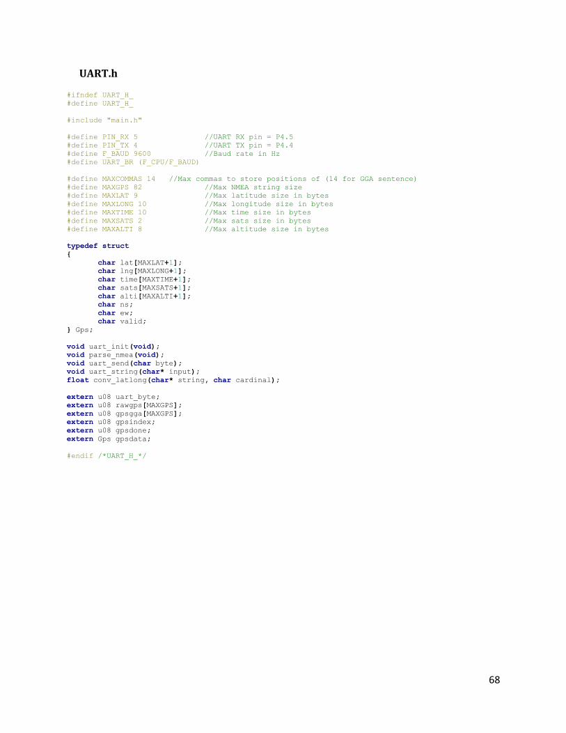
68
UART.h
#ifndef UART_H_
#define UART_H_
#include "main.h"
#define PIN_RX 5 //UART RX pin = P4.5
#define PIN_TX 4 //UART TX pin = P4.4
#define F_BAUD 9600 //Baud rate in Hz
#define UART_BR (F_CPU/F_BAUD)
#define MAXCOMMAS 14 //Max commas to store positions of (14 for GGA sentence)
#define MAXGPS 82 //Max NMEA string size
#define MAXLAT 9 //Max latitude size in bytes
#define MAXLONG 10 //Max longitude size in bytes
#define MAXTIME 10 //Max time size in bytes
#define MAXSATS 2 //Max sats size in bytes
#define MAXALTI 8 //Max altitude size in bytes
typedef struct
char lat[MAXLAT+1];
char lng[MAXLONG+1];
char time[MAXTIME+1];
char sats[MAXSATS+1];
char alti[MAXALTI+1];
char ns;
char ew;
char valid;
Gps;
void uart_init(void);
void parse_nmea(void);
void uart_send(char byte);
void uart_string(char* input);
float conv_latlong(char* string, char cardinal);
extern u08 uart_byte;
extern u08 rawgps[MAXGPS];
extern u08 gpsgga[MAXGPS];
extern u08 gpsindex;
extern u08 gpsdone;
extern Gps gpsdata;
#endif /*UART_H_*/
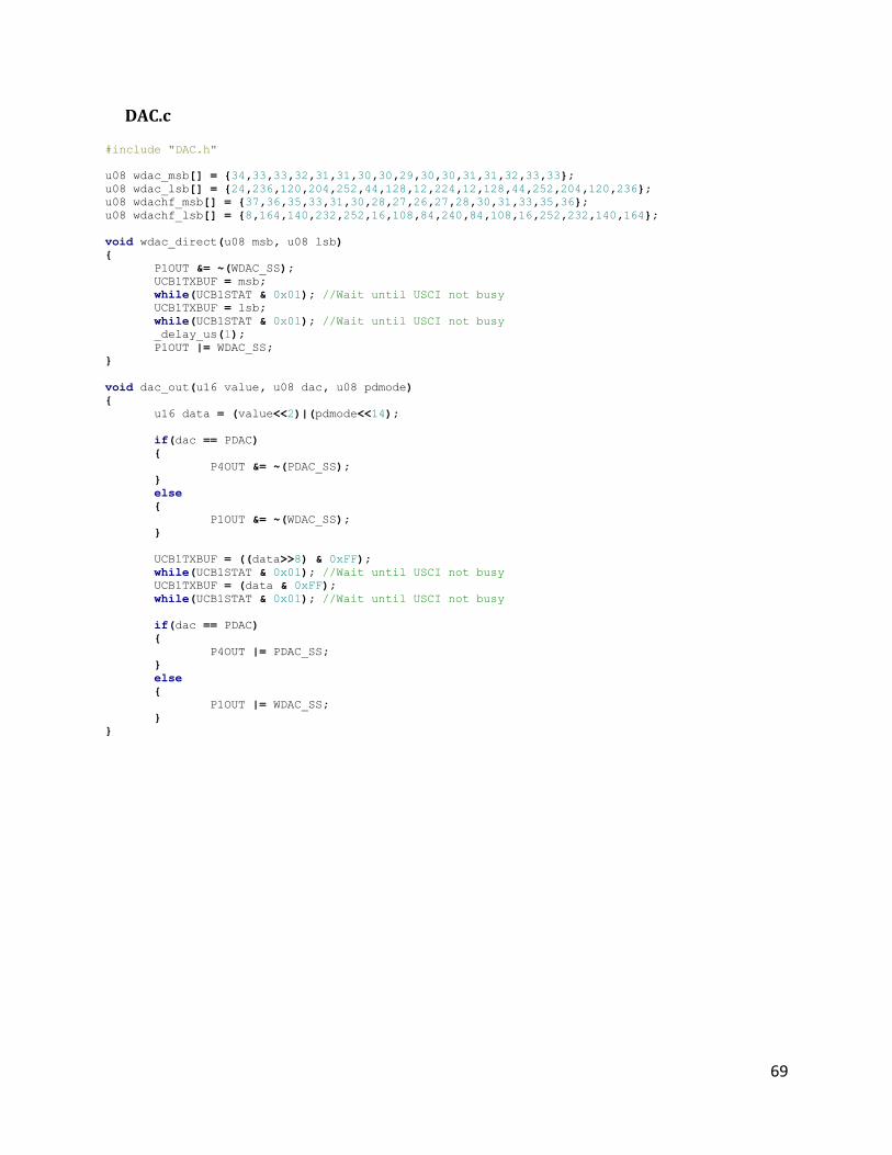
69
DAC.c
#include "DAC.h"
u08 wdac_msb[] = 34,33,33,32,31,31,30,30,29,30,30,31,31,32,33,33;
u08 wdac_lsb[] = 24,236,120,204,252,44,128,12,224,12,128,44,252,204,120,236;
u08 wdachf_msb[] = 37,36,35,33,31,30,28,27,26,27,28,30,31,33,35,36;
u08 wdachf_lsb[] = 8,164,140,232,252,16,108,84,240,84,108,16,252,232,140,164;
void wdac_direct(u08 msb, u08 lsb)
P1OUT &= ~(WDAC_SS);
UCB1TXBUF = msb;
while(UCB1STAT & 0x01); //Wait until USCI not busy
UCB1TXBUF = lsb;
while(UCB1STAT & 0x01); //Wait until USCI not busy
_delay_us(1);
P1OUT |= WDAC_SS;
void dac_out(u16 value, u08 dac, u08 pdmode)
u16 data = (value<<2)|(pdmode<<14);
if(dac == PDAC)
P4OUT &= ~(PDAC_SS);
else
P1OUT &= ~(WDAC_SS);
UCB1TXBUF = ((data>>8) & 0xFF);
while(UCB1STAT & 0x01); //Wait until USCI not busy
UCB1TXBUF = (data & 0xFF);
while(UCB1STAT & 0x01); //Wait until USCI not busy
if(dac == PDAC)
P4OUT |= PDAC_SS;
else
P1OUT |= WDAC_SS;

70
DAC.h
/* SPI Driver for TI DAC7311; must be used in conjunction
* with generic SPI driver after SPI initialization */
#ifndef DAC_H_
#define DAC_H_
#include "main.h"
#define PDAC_SS 0x40 //Power Control DAC Sync Pin = P4.6
#define WDAC_SS 0x20 //Waveform Generation DAC Sync Pin = P1.5
#define PDAC 0
#define WDAC 1
#define PD0 0 //Normal Operation
#define PD1 1 //Output 1k to GND
#define PD2 2 //Output 100k to GND
#define PD3 3 //Output Hi-Z
void dac_out(u16 value, u08 dac, u08 pdmode);
void wdac_direct(u08 msb, u08 lsb);
extern u08 wdac_msb[];
extern u08 wdac_lsb[];
extern u08 wdachf_msb[];
extern u08 wdachf_lsb[];
#endif /*DAC_H_*/

71
Nokia.c
#include "Nokia.h"
/* Internal Functions */
static void nlcd_line8(u08 x, u08 y, u08 height);
static void nlcd_line(u08 x, u08 y, u08 height);
/* Internal Framebuffer Functions */
#if NOKIA_FB == 1
static void nlcd_line8fb(u08 x, u08 y, u08 height, u08 fill);
static void nlcd_linefb(u08 x, u08 y, u08 height, u08 fill);
static void nlcd_linehfb(u08 x, u08 y, u08 h, u08 byte, u08 fill);
#endif
/* Internal Character Functions */
#if NOKIA_CHR == 1
static void nlcd_lineh(u08 x, u08 y, u08 h, u08 byte);
#endif
/* 3x5 character font */
#if NOKIA_CHR == 1
unsigned char chrarray[][3] =
0x00, 0x00, 0x00 // 20
,0x00, 0x17, 0x00 // 21 !
,0x03, 0x00, 0x03 // 22 "
,0x1E, 0x0A, 0x0F // 23 #
,0x14, 0x1F, 0x0A // 24 $
,0x09, 0x04, 0x12 // 25 %
,0x1E, 0x19, 0x0C // 26 &
,0x00, 0x03, 0x00 // 27 '
,0x0E, 0x11, 0x00 // 28 (
,0x00, 0x11, 0x0E // 29 )
,0x05, 0x02, 0x05 // 2a *
,0x04, 0x0E, 0x04 // 2b +
,0x10, 0x08, 0x00 // 2c ,
,0x04, 0x04, 0x04 // 2d -
,0x00, 0x10, 0x00 // 2e .
,0x18, 0x0E, 0x03 // 2f /
,0x1F, 0x11, 0x1F // 30 0
,0x12, 0x1F, 0x10 // 31 1
,0x19, 0x15, 0x12 // 32 2
,0x11, 0x15, 0x0B // 33 3
,0x07, 0x04, 0x1F // 34 4
,0x17, 0x15, 0x09 // 35 5
,0x1E, 0x15, 0x1D // 36 6
,0x19, 0x05, 0x03 // 37 7
,0x1B, 0x15, 0x1B // 38 8
,0x07, 0x05, 0x1F // 39 9
,0x00, 0x0A, 0x00 // 3a :
,0x10, 0x05, 0x00 // 3b ;
,0x04, 0x05, 0x00 // 3c <
,0x05, 0x05, 0x05 // 3d =
,0x00, 0x05, 0x04 // 3e >
,0x01, 0x15, 0x07 // 3f ?
,0x09, 0x15, 0x0E // 40 @
,0x1E, 0x05, 0x1E // 41 A
,0x1F, 0x15, 0x0A // 42 B
,0x0E, 0x11, 0x11 // 43 C
,0x1F, 0x11, 0x0E // 44 D
,0x1F, 0x15, 0x11 // 45 E
,0x1F, 0x05, 0x01 // 46 F
,0x0E, 0x11, 0x1D // 47 G
,0x1F, 0x04, 0x1F // 48 H
,0x11, 0x1F, 0x11 // 49 I
,0x11, 0x11, 0x0F // 4a J
,0x1F, 0x04, 0x1B // 4b K
,0x1F, 0x10, 0x10 // 4c L
,0x1F, 0x02, 0x1F // 4d M
,0x1F, 0x06, 0x1F // 4e N
,0x1F, 0x11, 0x1F // 4f O
,0x1F, 0x05, 0x02 // 50 P

72
,0x0F, 0x09, 0x1F // 51 Q
,0x1F, 0x05, 0x1A // 52 R
,0x12, 0x15, 0x09 // 53 S
,0x01, 0x1F, 0x01 // 54 T
,0x0F, 0x10, 0x1F // 55 U
,0x0F, 0x10, 0x0F // 56 V
,0x1F, 0x0C, 0x1F // 57 W
,0x1B, 0x04, 0x1B // 58 X
,0x03, 0x1C, 0x03 // 59 Y
,0x19, 0x15, 0x13 // 5a Z
,0x1F, 0x11, 0x00 // 5b [
,0x0B, 0x1C, 0x0B // 5c ¥
,0x00, 0x11, 0x1F // 5d ]
,0x02, 0x01, 0x02 // 5e ^
,0x10, 0x10, 0x10 // 5f _
,0x00, 0x01, 0x02 // 60 `
,0x18, 0x14, 0x1C // 61 a
,0x1F, 0x14, 0x08 // 62 b
,0x08, 0x14, 0x14 // 63 c
,0x08, 0x14, 0x1F // 64 d
,0x0C, 0x1A, 0x14 // 65 e
,0x04, 0x1E, 0x05 // 66 f
,0x14, 0x1A, 0x0E // 67 g
,0x1F, 0x04, 0x18 // 68 h
,0x00, 0x1A, 0x00 // 69 i
,0x10, 0x0D, 0x00 // 6a j
,0x1F, 0x08, 0x14 // 6b k
,0x00, 0x0F, 0x10 // 6c l
,0x1C, 0x08, 0x1C // 6d m
,0x1C, 0x04, 0x18 // 6e n
,0x1C, 0x14, 0x1C // 6f o
,0x1E, 0x0A, 0x04 // 70 p
,0x04, 0x0A, 0x1E // 71 q
,0x1C, 0x04, 0x04 // 72 r
,0x14, 0x1A, 0x0A // 73 s
,0x04, 0x1F, 0x04 // 74 t
,0x0C, 0x10, 0x1C // 75 u
,0x0C, 0x10, 0x0C // 76 v
,0x0C, 0x18, 0x0C // 77 w
,0x14, 0x08, 0x14 // 78 x
,0x16, 0x08, 0x06 // 79 y
,0x1A, 0x16, 0x12 // 7a z
,0x04, 0x0E, 0x11 // 7b
,0x00, 0x1F, 0x00 // 7c |
,0x11, 0x0E, 0x04 // 7d
,0x0C, 0x0C, 0x00 // 7e . (game ball)
;
#endif
void nlcd_data(u08 byte, u08 dc)
if(dc)
sbi(P1OUT,DC); //Set D/C'
else
cbi(P1OUT,DC);
cbi(P1OUT,SCE);
UCB1TXBUF = byte;
while(UCB1STAT & 0x01); //Wait until USCI not busy
_delay_us(1);
sbi(P1OUT,SCE);
void nlcd_init(void)
sbi(P1OUT,SCE);
sbi(P1OUT,RES);
_delay_us(1);
cbi(P1OUT,RES);
_delay_us(1);

73
sbi(P1OUT,RES);
nlcd_data(0x21,0); // LCD Extended Commands
nlcd_data((0x80|VOP),0); // Set LCD Vop (Contrast) (0x80 | Vop)
nlcd_data(0x04,0); // Set Temp coefficent
nlcd_data(0x14,0); // LCD bias mode 1:48
nlcd_data(0x20,0); // LCD Normal Commands
nlcd_data(0x0C,0); // LCD in normal mode. 0x0D for inverse
void nlcd_clear(void)
int i,j;
for(j=0;j<6;j++)
for(i=0;i<84;i++)
nlcd_data(0x00,1);
void nlcd_move(u08 x, u08 y)
if(x>83)
x=83;
if(y>5)
y=5;
nlcd_data((0x80|x),0);
nlcd_data((0x40|y),0);
void nlcd_line8(u08 x, u08 y, u08 height)
nlcd_move(x,(y>>3));
nlcd_data((((1<<height)-1)<<(y%8)),1);
void nlcd_line(u08 x, u08 y, u08 height)
u08 bank = (y>>3), i, h1, h2;
if((y+height)<=((bank+1)<<3))
nlcd_line8(x,y,height);
else
h1 = (((bank+1)<<3)-y);
h2 = (y+height)-(((y+height)>>3)<<3);
for(i=bank;i<((bank<5)?(((y+height)>>3)+1):6);i++)
if(i==bank)
nlcd_line8(x,y,h1);
else if(i==((y+height)>>3))
nlcd_line8(x,(i<<3),h2);
else
nlcd_line8(x,(i<<3),8);
void nlcd_box(u08 x, u08 y, u08 width, u08 height)
int i;
for(i=x;i<(x+width);i++)
nlcd_line(i,y,height);

74
/* LCD Framebuffer Functions */
#if NOKIA_FB == 1
void nlcd_line8fb(u08 x, u08 y, u08 height, u08 fill)
// Set address to x, y/8 (0<=y<=4)
if(fill)
framebuf[x][(y>>3)] |= (((1<<height)-1)<<(y%8)); // Make line of height with (1<<height)-1,
with position y%8
else
framebuf[x][(y>>3)] &= ~(((1<<height)-1)<<(y%8)); // Make line of height with (1<<height)-
1, with position y%8
void nlcd_linefb(u08 x, u08 y, u08 height, u08 fill)
u08 bank = (y>>3), i, h1, h2;
if((y+height)<((bank+1)<<3))
nlcd_line8fb(x,y,height,fill);
else
h1 = (((bank+1)<<3)-y); // Height of the top byte
h2 = (y+height)-(((y+height)>>3)<<3); // Height of the bottom byte
for(i=bank;i<((bank<5)?(((y+height)>>3)+1):6);i++)
if(i==bank)
nlcd_line8fb(x,y,h1,fill);
else if(i==((y+height)>>3))
nlcd_line8fb(x,(i<<3),h2,fill);
else
nlcd_line8fb(x,(i<<3),8,fill);
void nlcd_boxfb(u08 x, u08 y, u08 width, u08 height, u08 fill)
int i;
for(i=x;i<(x+width);i++)
nlcd_linefb(i,y,height,fill);
void nlcd_clearfb(void)
int i,j;
nlcd_move(0,0);
for(j=0;j<6;j++)
for(i=0;i<84;i++)
framebuf[i][j] = 0x00;
u08 nlcd_read_pixel(u08 x, u08 y)
return ((framebuf[x][(y>>3)] & (1<<(y%8)))>>(y%8));
void nlcd_write_frame(unsigned char frame[84][6])
int i,j;
for(j=0;j<6;j++)

75
for(i=0;i<84;i++)
nlcd_data(frame[i][j],1);
#endif
/* Character/Font Functions */
#if NOKIA_CHR == 1
void nlcd_chr5(u08 x, u08 y, u08 chr)
u08 i;
for(i=0;i<3;i++)
nlcd_lineh((x+i),y,5,chrarray[(chr-0x20)][i]);
nlcd_lineh((x+3),y,5,0x00); //Add space between consecutive characters
void nlcd_string(u08 x, u08 y, char* input)
u08 i;
for(i=0;input[i]!=0x00;i++)
nlcd_chr5((x+(i<<2)),y,input[i]);
void nlcd_s16(u08 x, u08 y, s16 var)
u08 i=1,j; //Initialize i to 1 for case of var < 9
char chr[5];
if(var < 0)
nlcd_chr5(x,y,'-');
var *= -1;
if(var > 9)
for(i=0; var>0; var/=10,i++)
chr[i] = 0x30 + (var%10);
else
chr[0] = var + 0x30;
for(j=0;i>0;i--,j++)
nlcd_chr5(x+(j<<2),y,chr[(i-1)]);
void nlcd_s16z(u08 x, u08 y, s16 var)
u08 i,j;
char chr[5];
chr[4] = (var/10000)%10+0x30;
chr[3] = (var/1000)%10+0x30;
chr[2] = (var/100)%10+0x30;
chr[1] = (var/10)%10+0x30;
chr[0] = var%10+0x30;
for(j=0,i=4;i>0;i--,j++) //i=5 normally, i=4 eliminates excess 0
nlcd_chr5(x+(j<<2),y,chr[(i-1)]);

76
#if NOKIA_FB == 1
void nlcd_chr5fb(u08 x, u08 y, u08 chr, u08 fill)
u08 i;
for(i=0;i<3;i++)
nlcd_linehfb((x+i),y,5,chrarray[(chr-0x20)][i],fill);
nlcd_linehfb((x+3),y,5,0x00,fill); //Add space between consecutive characters
void nlcd_stringfb(u08 x, u08 y, char* input, u08 fill)
u08 i;
for(i=0;input[i]!=0x00;i++)
nlcd_chr5fb((x+(i<<2)),y,input[i],fill);
void nlcd_s16fb(u08 x, u08 y, s16 var, u08 fill)
u08 i=1,j;
char chr[5];
if(var < 0)
nlcd_chr5fb(x,y,'-',fill);
var *= -1;
if(var > 9)
for(i=0; var>0; var/=10,i++)
chr[i] = 0x30 + (var%10);
else
chr[0] = var + 0x30;
for(j=0;i>0;i--,j++)
nlcd_chr5fb((x+(j<<2)),y,chr[(i-1)],fill);
#endif
#endif
/* Internal Functions */
void nlcd_lineh(u08 x, u08 y, u08 h, u08 byte)
u08 bank = (y>>3), h1, h2;
nlcd_move(x,bank);
if((y+h)<((bank+1)<<3)) //If data doesn't overflow to next y row
nlcd_data((byte<<(y%8)),1);
else
h1 = (byte<<(y%8)); //Data for upper half
h2 = (byte>>(h-((y+h)-(((y+h)>>3)<<3)))); //Data for lower half (on next row)
nlcd_data(h1,1);
nlcd_move(x,bank+1);
nlcd_data(h2,1);

77
#if NOKIA_FB == 1
void nlcd_linehfb(u08 x, u08 y, u08 h, u08 byte, u08 fill)
u08 bank = (y>>3), h1, h2;
if((y+h)<((bank+1)<<3)) //If data doesn't overflow to next y row
if(fill)
framebuf[x][bank] |= ((byte<<(y%8)));
else
framebuf[x][bank] &= ~((byte<<(y%8)));
else
h1 = (byte<<(y%8)); //Data for upper half
h2 = (byte>>(h-((y+h)-(((y+h)>>3)<<3)))); //Data for lower half (on next row)
if(fill)
framebuf[x][bank] |= (h1);
framebuf[x][bank+1] |= (h2);
else
framebuf[x][bank] &= ~(h1);
framebuf[x][bank+1] &= ~(h2);
#endif

78
Nokia.h
#ifndef NOKIA_H_
#define NOKIA_H_
#include "main.h"
//Dependencies: SPI.c, SPI.h
/* User Defines/Constants */
#define NOKIA_FB 0 //Use framebuffer and assoc. functions (requires 94B constant data)
#define NOKIA_CHR 1 //Use characters and assoc. functions (requires 504B variable data)
#define SCE 6 //P1.6 = SCE'
#define RES 3 //P1.3 = RES'
#define DC 1 //P1.1 = D/C'
#define VOP 0x1C //Contrast value ranging between 0x00-0x4F
#if NOKIA_FB == 1
unsigned char framebuf[84][6];
#endif
/* User Functions */
void nlcd_data(u08 byte, u08 dc); //Writes a data byte to the LCD
void nlcd_init(void); //Initializes LCD
void nlcd_clear(void); //Writes 0's to all LCD pixels
void nlcd_move(u08 x, u08 y); //Moves cursor to position 0<=x<=83, 0<=y<=5
void nlcd_box(u08 x, u08 y, u08 width, u08 height); //Draws a box with upper left corner at
(x,y), of width x, height y
/* Framebuffered Functions */
#if NOKIA_FB == 1
void nlcd_boxfb(u08 x, u08 y, u08 width, u08 height, u08 fill); //Draws a box (filled in or no
fill) at x,y of width x, height y
u08 nlcd_read_pixel(u08 x, u08 y); //Returns a 1 if the pixel at x,y in the framebuffer is filled
(dark)
void nlcd_clearfb(void); //Clears framebuffer (same as lcd_clear for framebuffer)
void nlcd_write_frame(unsigned char frame[84][6]); //Updates LCD memory with local framebuffer
contents
#endif
/* Font Functions */
#if NOKIA_CHR == 1
void nlcd_chr5(u08 x, u08 y, u08 chr);
void nlcd_string(u08 x, u08 y, char* input);
void nlcd_s16(u08 x, u08 y, s16 var);
void nlcd_s16z(u08 x, u08 y, s16 var);
#if NOKIA_FB == 1
void nlcd_chr5fb(u08 x, u08 y, u08 chr, u08 fill);
void nlcd_stringfb(u08 x, u08 y, char* input, u08 fill);
void nlcd_s16fb(u08 x, u08 y, s16 var, u08 fill);
#endif
#endif
#endif /*NOKIA_H_*/


![APRS is a registered trademark Bob Bruninga, WB4APR 1 APRS Introduction to APRS! [Feb 2009] DCC 2008 Maps – Mobiles - Users Human to human info exchange!](https://static.fdocuments.in/doc/165x107/56649d775503460f94a59c46/aprs-is-a-registered-trademark-bob-bruninga-wb4apr-1-aprs-introduction-to.jpg)

