
All Digital on Chip Process Sensor Using Ratioed Inverter ... · Inverter Based Ring Oscillator 1G....
7
IJIRMPS | Volume 6, Issue 4, 2018 ISSN: 2349-7300 IJIRMPS1807090 Website : www.ijirmps.org Email : [email protected] 551 All Digital on Chip Process Sensor Using Ratioed Inverter Based Ring Oscillator 1 G. Rajesh, 2 G. Guru Prakash, 3 M.Yachendra, 4 O.Venka babu, 5 Mr. G. Kiran Kumar 1,2,3,4 Final year, B. Tech, Department of Electronics & Communications, 5 Assistant Professor Geethanjali Institute of Science & Technology, Nellore. Abstract: In this project, an all-digital ON-chip process sensor using a ratioed inverter-based ring oscillator is proposed. Two types of the ratioed inverter-based ring oscillators, nMOS and pMOS types are proposed to sense process variation. The nMOS (pMOS)-type ring oscillator is designed to improve its sensitivity to the process variation in the nMOS (pMOS) transistors using the ratioed inverter that consists of only nMOS (pMOS) transistors. A compact process sensor can be realized using only these two types of ring oscillators. Keywords: All-digital sensor, process variations, ratioed inverter, ring oscillator. I. INTRODUCTION Semiconductor technologies have been continually improved to nanometre-scale geometries. The device parameters of MOSFETs, such as the threshold voltage, channel length, oxide thickness, and mobility, are affected by process variations originating from the manufacturing process. The influence of these variations on the MOSFET’s device parameters increases as the process technology is scaled. Accordingly, the effects of process variation can cause performance degradation or even a chip malfunction. Thus, the circuit designer should consider the effects of process variation for improving the yield or circuit performance. There are two design approaches for analyzing the effects of process variation. A static timing analysis (STA) is widely used to consider the process variation before fabrication. The STA simulates the delay in the circuit and analyzes the results to guarantee proper operation of the circuit at all process corners. MOTIVATION To reduce power consumption and radiation effects in conventional Digital Signal Processor architecture and WSN.A low cost implementation of Digital Signal Processor for WSN. To reduce the complexity of system. 1.2 EXISTING SYSTEM There are two design approaches for analyzing the effects of process variation. A static timing analysis (STA) is widely used to consider the process variation before fabrication. The STA simulates the delay in the circuit and analyzes the results to guarantee proper operation of the circuit at all process corners. However, the design parameters should have sufficient margins to guarantee proper operation because the design parameters in an STA are determined by predicting the worst case of the process variation for achieving the maximum yield. On the other hand, an ON-chip process sensor is used to identify the process variation after fabrication.
Transcript of All Digital on Chip Process Sensor Using Ratioed Inverter ... · Inverter Based Ring Oscillator 1G....
IJIRMPS | Volume 6, Issue 4, 2018 ISSN: 2349-7300
IJIRMPS1807090 Website : www.ijirmps.org Email : [email protected] 551
All Digital on Chip Process Sensor Using Ratioed
Inverter Based Ring Oscillator
1G. Rajesh, 2G. Guru Prakash, 3M.Yachendra, 4O.Venka babu, 5Mr. G. Kiran Kumar
1,2,3,4Final year, B. Tech, Department of Electronics & Communications, 5Assistant Professor
Geethanjali Institute of Science & Technology, Nellore.
Abstract: In this project, an all-digital ON-chip process sensor using a ratioed inverter-based ring oscillator is proposed.
Two types of the ratioed inverter-based ring oscillators, nMOS and pMOS types are proposed to sense process variation.
The nMOS (pMOS)-type ring oscillator is designed to improve its sensitivity to the process variation in the nMOS (pMOS)
transistors using the ratioed inverter that consists of only nMOS (pMOS) transistors. A compact process sensor can be
realized using only these two types of ring oscillators.
Keywords: All-digital sensor, process variations, ratioed inverter, ring oscillator.
I. INTRODUCTION
Semiconductor technologies have been continually improved to nanometre-scale geometries. The device parameters of
MOSFETs, such as the threshold voltage, channel length, oxide thickness, and mobility, are affected by process variations
originating from the manufacturing process. The influence of these variations on the MOSFET’s device parameters increases as the
process technology is scaled. Accordingly, the effects of process variation can cause performance degradation or even a chip
malfunction. Thus, the circuit designer should consider the effects of process variation for improving the yield or circuit
performance. There are two design approaches for analyzing the effects of process variation. A static timing analysis (STA) is
widely used to consider the process variation before fabrication. The STA simulates the delay in the circuit and analyzes the results
to guarantee proper operation of the circuit at all process corners.
MOTIVATION
To reduce power consumption and radiation effects in conventional Digital Signal Processor architecture and WSN.A low cost
implementation of Digital Signal Processor for WSN. To reduce the complexity of system.
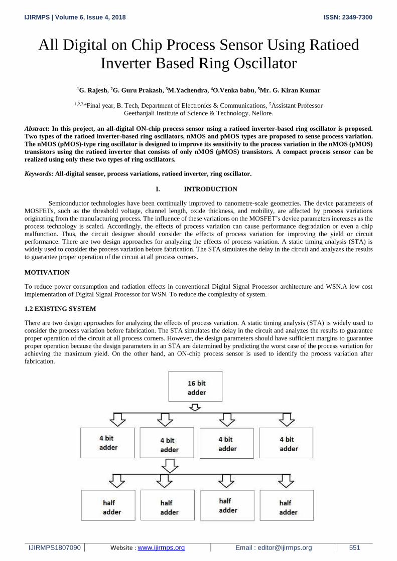
1.2 EXISTING SYSTEM
There are two design approaches for analyzing the effects of process variation. A static timing analysis (STA) is widely used to
consider the process variation before fabrication. The STA simulates the delay in the circuit and analyzes the results to guarantee
proper operation of the circuit at all process corners. However, the design parameters should have sufficient margins to guarantee
proper operation because the design parameters in an STA are determined by predicting the worst case of the process variation for
achieving the maximum yield. On the other hand, an ON-chip process sensor is used to identify the process variation after
fabrication.

IJIRMPS | Volume 6, Issue 4, 2018 ISSN: 2349-7300
IJIRMPS1807090 Website : www.ijirmps.org Email : [email protected] 552
II. PROPOSED SYSTEM
In this project, a process sensor that uses the proposed ratioed inverter-based ring oscillator is proposed to effectively
characterize spatially correlated process variation. The proposed ratioed inverter enhances the process sensitivity with a com-pact
size and solves the problems of the previous structures. Thus, the proposed all-digital process sensor is a practical solution for ON-
chip implementation with post silicon tuning. The proposed ratioed inverter consists of the same type of MOSFET for the load
transistor (MN Load and MP Load) and the driver transistor (MN Driver and MP Driver)to improve the process sensitivity.
A. BASIC STRUCTURE OF THE RING OSCILLATOR
Ring-oscillator-based process sensors use oscillation frequency as a process metric. Because process sensitivity is the change in
oscillation frequency according to process variation, the load capacitance of the delay cell in the previous ring oscillator is modified
to improve the change in the oscillation frequency. In the proposed ring oscillator, the process sensitivity is enhanced by the
proposed ratioed inverter. The proposed ratioed inverter consists of the same type of MOSFET for the load transistor (MN Load
and MP Load) and the driver transistor (MN Driver and MP Driver) to improve the process sensitivity, as shown in Fig below. The
load transistor is diode connected, and its gate terminal serves as the input of the ratioed inverter. The variation in the propagation
delay of each ratioed inverter can indicate the process variation in its MOSFET type because the propagation delay changes
according to the driving strength of the MOSFET type. However, sensing the process variation by directly measuring the
propagation delay of the ratioed inverter is very difficult and requires a highly precise timing measurement technique because the
propagation delay is very small.
Thus, for easier process variation sensing, the ring oscillator is constructed using the ratioed inverter. Then, the oscillation frequency
of the ring oscillator is used as the process-variation-sensing metric.
Fig:3.1.1: Strutures of the (a) nMOS-type ratioed inverter and (b) pMOS-type ratioed Inverter
However, the output voltage of the nMOS (or pMOS) ratioed inverter, VO,N (or VO,P), cannot achieve the full output
voltage swing because the load transistor is always turned ON owing to the diode connection. Thus, if the ring oscillator is
constructed using only ratioed inverters, the output of the ring oscillator gradually stops oscillating and converges to a certain
voltage, which is determined by the ratio of the pullup and pull-down driving strengths of the ratioed inverter. Thus, as shown in
Fig below, a CMOS inverter is added to the output of the ratioed inverter as a buffer to achieve the full output swing. A set of nMOS
(or pMOS)-type delay cells for the process-dependent delay and one NAND gate for the oscillation operation compose the nMOS
(or pMOS)-type ring oscillator. When the high level of START is applied to the NAND gate, the ring oscillator begins oscillating.
Then the process-dependent delay from the delay cell is represented in the output of the NAND gate (NANDOUT).
B. PROCESS SENSIIVE PULSE WIDTH
In the proposed ring oscillator, the pulse width of the oscillation period is used as a process metric instead of the entire
oscillation period because of the following characteristics of the proposed ratioed inverter in the next paragraph. First, the
propagation delays of the ratioed and CMOS inverters in the delay cell need to be examined. There are two types of propagation

IJIRMPS | Volume 6, Issue 4, 2018 ISSN: 2349-7300
IJIRMPS1807090 Website : www.ijirmps.org Email : [email protected] 553
delays: rising and falling propagation delays. The rising (falling) propagation delay is the time required for the rising (falling) edge
to propagate through the delay cell. When the falling (rising) edge is applied to an nMOS (pMOS)-type delay cell, the nMOS
(pMOS) driver transistor is turned OFF and the nMOS (pMOS) transistor of the CMOS inverter is then turned ON. On the other
hand, when the rising (falling) edge is applied to an nMOS (pMOS) type delay cell, the driver transistor is turned ON and the pMOS
(nMOS) transistor of the CMOS inverter is then turned ON. Because the falling (rising) edge propagates through the nMOS
(pMOS)-type delay cell without turning ON the pMOS (nMOS) transistor in the CMOS inverter, the falling (rising) propagation
delay of the nMOS (pMOS)-type delay cell, tPG,F,N (tPG,R,P), is used to sense the nMOS (pMOS)-transistor process variation.

IJIRMPS | Volume 6, Issue 4, 2018 ISSN: 2349-7300
IJIRMPS1807090 Website : www.ijirmps.org Email : [email protected] 554
Block Diagram:
In order to verify the operation of the proposed sensor, a test structure is implemented. The test structure is partitioned into
two blocks: a process-sensing block and time-to-digital converter (TDC) block, The processsensing block consists of ring oscillator
units, a DEMUX, and an MUX, and it generates a process-dependent output ROOUT. The ring oscillator units consist of nMOS-
and\ pMOS-type ring oscillators with a various number of stages. Each ring oscillator unit is selected to start oscillation by the
selection signal, SELRO, and the output of the selected ring oscillator is connected to the TDC block through the MUX.
The TDC block consists of two counters—width and cycle counters—with a cycle decider. The width counter converts the
high pulsewidth of the output of the ring oscillator, PWROOUT, into a digital code CODEOUT, and the cycle counter counts the
number of ROOUT cycles, CNTRO. The cycle decider generates ENDCNT to stop both counters when CNTRO becomes the same
as the predetermined number of ROOUT cycles, CNTSTOP.
The operation of the proposed.
III. SOFTWARE REQUIREMENTS
A. MICROWIND
To Create a Project • Open the Schematic Editor in Micro wind (DSCH3). Click on the transistor symbol in the Symbol Library on the right.
• Instantiate NMOS or PMOS transistors from the symbol library and place them in the editor window.
The dsch2 program is a logic editor and simulator. Dsch2 is used to validate the architecture of the logic circuit before the
microelectronics design is started. Dsch2 provides a user friendly environment for hierarchical logic design, and simulation with
delay analysis, which allows the design and validation of complex logic structures. A key innovative feature.
A. LANGUAGE VERILOG
In the semiconductor and electronic outline industry, Verilog is an equipment portrayal language (HDL) used to show
electronic frameworks. Verilog HDL, not to be mistaken for VHDL (a contending dialect), is most generally utilized as a part of
the outline, confirmation, and usage of digital rationale chips at the register-exchange level of reflection. It is likewise utilized as a
part of the confirmation of analog and blended sign circuits.

IJIRMPS | Volume 6, Issue 4, 2018 ISSN: 2349-7300
IJIRMPS1807090 Website : www.ijirmps.org Email : [email protected] 555
IV. RESULTS AND ANALYSIS
A. LAYOUT DIAGRAM OF RING OSCILLATOR
Fig: Layout Diagram
The above figure shows the layout diagram of the Ring oscillator. It is the combination of the PMOS and NMOS Ring oscillators.
B . VOLTAGE VS TIME:
Fig: Voltage vs time
In the out 1 when the time increases the voltage will be in the sinusoidal form.In the in1 when the time increases the voltage
increases to the peak value and suddenly reaches to zero. It shows the triangular waveform
4.1 VOLTAGE AND CURRENTS:

IJIRMPS | Volume 6, Issue 4, 2018 ISSN: 2349-7300
IJIRMPS1807090 Website : www.ijirmps.org Email : [email protected] 556
4.2 FREQUENCY VS TIME:
4.3 VOLTAGE VS VOLTAGE:
4.4 EYE DIAGRAM :

IJIRMPS | Volume 6, Issue 4, 2018 ISSN: 2349-7300
IJIRMPS1807090 Website : www.ijirmps.org Email : [email protected] 557
V. ADVANTAGES
The output of relaxation oscillators depends on the time constant. Hence it can be used in circuits where time is required.
As they produce non-sinusoidal output, hence they are used extensively in digital circuits.
They have a large and linear tuning range that is often convenient and sometimes crucial for Frequency Modulation (FM) with
low distortion.
VI. APPLICATIONS
The voltage-controlled oscillator in most phase-locked loops is built from a ring oscillator.
Jitter of ring oscillators is commonly used in hardware random number generators.
A ring oscillator is often used to demonstrate a new hardware technology, analogous to the way a hello world program is often
used to demonstrate a new software technology
Many wafers include a ring oscillator as part of the scribe line test structures. They are used during wafer testing to measure the
effects of manufacturing process variations.
Ring oscillators can also be used to measure the effects of voltage and temperature on a Chip
VII. CONCLUSION
In this project, an all-digital ON-chip process-variation sensing circuit using a ratioed inverter-based ring oscillator is
proposed. The proposed ratioed inverter-based ring oscillator improves the process sensitivity with a compact size. In addition, the
time-to-digital conversion provides measurement results as a digital code that can be easily used to perform postsilicon tuning of
the ON-chip blocks, such as in the adaptive body bias or adaptive supply voltage technique.
The test chip is fabricated using the 0.13-μm CMOS process technology to verify the proposed process sensor. The
proposed process sensor achieves a significantly improved process sensitivity. The verification results using a body bias show that
the average inaccuracy between the simulation and measurement results appears to be 0.71%. Thus, it is confirmed that the proposed
process sensor works correctly for the various process corners. The proposed process sensor can be useful as an ON-chip process
sensor for the postsilicon tuning technique.
REFERENCES
1. K. J. Kuhn, “Reducing variation in advanced logic technologies: Approaches to process and design for manufacturability of
nanoscale CMOS,” in Proc. IEEE Int. Electron Devices Meeting (IEDM), Dec. 2007, pp. 471–474.
2. A. Zjajo, M. J. Barragan, and J. P. de Gyvez, “Low-power die-level process variation and temperature monitors for yield analysis
and optimization in deep-submicron CMOS,” IEEE Trans. Instrum. Meas., vol. 61, no. 8, pp. 2212–2221, Aug. 2012.
3. D. Kim, C. Cho, J. Kim, J.-O. Plouchart, R. Trzcinski, and D. Ahlgren, “CMOS mixedsignal circuit process variation sensitivity
characterization for yield improvement,” in Proc. IEEE Custom Integr. Circuits Conf. (CICC), Sep. 2006, pp. 365–368.
4. D. Blaauw, K. Chopra, A. Srivastava, and L. Scheffer, “Statistical timing analysis: From basic principles to state of the art,” IEEE
Trans. Comput.-Aided Design Integr. Circuits Syst.,
vol. 27, no. 4, pp. 589–607, Apr. 2008.