All Chapter 2 Slides in ch2.pdf
92
Chapter 2 Learning to Use the Hardware and Software Contents Slide 2-1 A Sample Linker Command File Slide 2-2 Sample Linker Command File (cont. 1) Slide 2-3 Sample Linker Command File (cont. 2) Slide 2-4 C Program to Use as a Starting Point Slide 2-5 Program for Starting Point (cont. 1) Slide 2-6 Program for Starting Point (cont. 2) Slide 2-7 Program for Starting Point (cont. 3) Slide 2-8 Program for Starting Point (cont. 4) Slide 2-9 Program for Starting Point (cont. 5) Slide 2-10 Program for Starting Point (cont. 6) Slide 2-11 Program for Starting Point (cont. 7) Slide 2-12 Program for Starting Point (cont. 8) Slide 2-13 Getting Samples to and from the Codec Slide 2-14 The Function DSK6713 AIC23 write() Slide 2-15 Receiving Samples from the Codec Slide 2-16 AIC23 Sampling Rates Slide 2-17 AIC23 Analog Interface Properties Slide 2-18 AIC23 ADC and DAC Filter Responses Slide 2-19 Creating a CCS Project for dskstart32.c Slide 2-20 Creating a CCS Project for dskstart32.c
-
Upload
phamkhuong -
Category
Documents
-
view
251 -
download
0
Transcript of All Chapter 2 Slides in ch2.pdf

Chapter 2 Learning to Use theHardware and Software
Contents
Slide 2-1 A Sample Linker Command FileSlide 2-2 Sample Linker Command File (cont. 1)Slide 2-3 Sample Linker Command File (cont. 2)Slide 2-4 C Program to Use as a Starting PointSlide 2-5 Program for Starting Point (cont. 1)Slide 2-6 Program for Starting Point (cont. 2)Slide 2-7 Program for Starting Point (cont. 3)Slide 2-8 Program for Starting Point (cont. 4)Slide 2-9 Program for Starting Point (cont. 5)Slide 2-10 Program for Starting Point (cont. 6)Slide 2-11 Program for Starting Point (cont. 7)Slide 2-12 Program for Starting Point (cont. 8)Slide 2-13 Getting Samples to and from the CodecSlide 2-14 The Function DSK6713 AIC23 write()Slide 2-15 Receiving Samples from the CodecSlide 2-16 AIC23 Sampling RatesSlide 2-17 AIC23 Analog Interface PropertiesSlide 2-18 AIC23 ADC and DAC Filter ResponsesSlide 2-19 Creating a CCS Project for dskstart32.cSlide 2-20 Creating a CCS Project for dskstart32.c

(cont. 1)Slide 2-21 Creating a CCS Project for dskstart32.c
(cont. 2)Slide 2-21 Build Options for Code ComposerSlide 2-22 Build Options for CCS (cont. 1)Slide 2-23 Build Options for CCS (cont. 2)Slide 2-24 Build Options for CCS (cont. 3)
Slide 2-24 A Simple First Experiment
Slide 2-25 Simple First Experiment (cont. 1)Slide 2-26 Simple First Experiment (cont. 2)Slide 2-27 Simple First Experiment (cont. 3)Slide 2-28 McBSP PropertiesSlide 2-29 McBSP Block DiagramSlide 2-30 McBSP Transmitter Block DiagramSlide 2-31 Operation of Serial Port TransmitterSlide 2-32 McBSP Receiver Block DiagramSlide 2-33 Operation of the Serial Port ReceiverSlide 2-34 C Code for Polling Stereo ReadSlide 2-35 C Code for Polling Stereo Write
Slide 2-36 Experiment 2.2 Sines by Polling
Slide 2-37 Experiment 2.2 (cont.)Slide 2-38 Generating Samples of a Sine Wave
2-ii

Slide 2-39 Sample Program Segment for PollingSlide 2-40 Some Important Information
Slide 2-41 Using Interrupts to Generate SinesSlide 2-42 Using Interrupts (cont. 1)Slide 2-43 Default CPU Interrupt SourcesSlide 2-44 Interrupt SourcesSlide 2-45 Interrupt Sources (cont.)Slide 2-46 External Interrupt SourcesSlide 2-47 Interrupt Control RegistersSlide 2-48 Conditions for an InterruptSlide 2-49 What Happens with an InterruptSlide 2-50 What Happens with an Interrupt (cont.)Slide 2-51 Example of an ISFPSlide 2-52 C Interrupt Service RoutinesSlide 2-53 Using the dsk6713bsl32.lib Interrupt
FunctionsSlide 2-54 Selected Library Interrupt FunctionsSlide 2-55 Installing a C ISR
Slide 2-56 Experiment 2.3 Interrupts
Slide 2-57 Sample Program Segment forInterrupts
Slide 2-58 Sample Program for Ints (cont. 1)Slide 2-59 Sample Program for Ints (cont. 2)
2-iii

Slide 2-60 Sample Program for Ints (cont. 3)
Slide 2-61 Enhanced DMA (EDMA)
Slide 2-62 EDMA OverviewSlide 2-63 EDMA Overview (cont.)Slide 2-64 EDMA Event SelectionSlide 2-65 Registers for Event ProcessingSlide 2-66 Default EDMA EventsSlide 2-67 EDMA Event Selection (1)Slide 2-68 EDMA Event Selection (2)Slide 2-69 EDMA Event Selection (3)Slide 2-70 The Parameter RAM (PaRAM)Slide 2-71 The OPT Field in the (PaRAM)Slide 2-72 Contents of the PaRAMSlide 2-73 Synchronization of EDMA TransfersSlide 2-74 Synchronization of Transfers (cont.)Slide 2-75 Linking EDMA TransfersSlide 2-76 Linking EDMA Transfers (cont.)Slide 2-77 EDMA Interrupts to the CPUSlide 2-78 Chaining EDMA Channels
Slide 2-79 Experiment 2.4 EDMA
Slide 2-80 Experiment 2.4 EDMA (cont.)Slide 2-81 Example EDMA Code Segment
2-iv

Slide 2-82 EDMA Code Segment (cont. 1)Slide 2-83 EDMA Code Segment (cont. 2)Slide 2-84 EDMA Code Segment (cont. 3)Slide 2-85 EDMA Code Segment (cont. 4)Slide 2-86 EDMA Code Segment (cont. 4)Slide 2-87 EDMA Code Segment (cont. 5)
2-v

✬
✫
✩
✪
Chapter 2
Learning to Use the Hardware and Software
Tools by Generating a Sine Wave
The directory C:\C6713dsk contains two example files
that you can use as a starting point for all your
projects.
A Sample Linker Command File
/***************************************************/
/* File dsk6713.cmd
This linker command file can be used as the
starting point for linking programs for the
TMS320C6713 DSK. It assumes everything fits into
internal RAM. If that’s not true, map some
sections to the external SDRAM.
****************************************************/
-c
-heap 0x1000
-stack 0x1000
-i "c:\Program Files\C6xCSL\lib_3x"
-i c:\c6713dsk\dsk6713bsl32\lib
-lrts6700.lib
-ldsk6713bsl32.lib
2-1

✬
✫
✩
✪
A Sample Linker Command File
(cont. 1)
-lcsl6713.lib
_HWI_Cache_Control = 0; /* For DSP BIOS */
MEMORY
{
VECS: origin = 0x0, len = 0x00000260
/* interrupt vectors and interrupt
service routine jump table in internal
L2 RAM */
PMEM: origin = 0x00000260, len = 0x0002FDA0
/* Remainder of 192 kB (0x30000 byte)
L2 internal RAM */
BMEM: origin = 0x80000000, len = 0x01000000
/* CE0, SDRAM, 16 MBytes */
FLASH: origin = 0x90000000, len = 0x40000
/* 256 Kbytes flash mem */
}
SECTIONS
{
.intvecs: load = 0x00000000
/* Interrupt vectors included */
/* by using intr_reset() */
.text: load = PMEM /* Executable code */
.const: load = PMEM /* Initialized constants*/
2-2

✬
✫
✩
✪
A Sample Linker Command File
(cont. 2)
.bss: load = PMEM /* Global and static
variables*/
.data: load = PMEM/* Data from .asm programs*/
.cinit: load = PMEM/* Tables for initializing
variables and constants */
.pinit: load = PMEM /* Pointers to
initialization functions */
.stack: load = PMEM /* Stack for local
variables */
.far: load = PMEM /* Global and static
variables declared far */
.sysmem: load = PMEM /* Used by malloc, etc.
(heap) */
.cio: load = PMEM /* For C I/O functions */
.csldata: load = PMEM
.switch: load = PMEM
}
You will shortly see how to supply this information to the
linker by entering it into your CCS project “Build Options.”
2-3

✬
✫
✩
✪
C Program to Use as a Starting Point
When CCS is commanded to run your program, it
first uses the file DSK6713.ccxml in your Project
Explorer window to execute the GEL file
dsk6713.gel in the directory
C:\ti\ccsv5\ccs_base\emulation\boards\
dsk6713\gel
which
• defines a memory map
• sets some CPLD registers
• initializes the EMIF for the memory on the
C6713 DSK.
The program C:\c6713dsk\dskstart32.c can be
used as a starting point for writing C6713 DSK
applications. It contains the code necessary to:
• further initialize the DSK board
• initialize the TMS320C6713 McBSPs
• initialize the AIC 23 codec.
2-4

✬
✫
✩
✪
C Program to Use as a Starting Point
(cont. 1)
The program dskstart32.c uses functions from
the UMD modified DSK Board Support Library
(BSL), C:\c6713dsk\dsk6713bsl32.lib, to
continue the initialization. You can find detailed
documentation for the BSL by navigating to
C:\6713\docs\hlp with Windows Explorer or
My Computer and double clicking on
c6713dsk.hlp and then clicking on Software.
The file c6713dsk.hlp also contains detailed
information about the DSK hardware.
The modified library, its header files, and sources
are in the directories:
C:\c6713dsk\dsk6713bsl32\lib
C:\c6713dsk\dsk6713bsl32\include
C:\c6713dsk\dsk6713bsl32\sources
\dsk6713bsl.zip.
2-5

✬
✫
✩
✪
C Program to Use as a Starting Point
(cont. 2)
∗ The program dskstart32.c first initializes the
board support library by calling DSK6713_init()
who’s source code is in the BSL file dsk6713.c.
This
• initalizes the chip’s PLL
• configures the EMIF based on the DSK
version
• sets the CPLD registers to a default state
∗ Next dskstart32.c initializes the interrupt
controller registers and installs the default
interrupt service routines by calling the function
intr_reset() in the UMD added file DSKintr.c.
This:
• clears GIE and PGIE
• disables all interrupts except RESET in IER
• clears the flags in the IFR for the the
maskable interrupts INT4 - INT15
2-6

✬
✫
✩
✪
C Program to Use as a Starting Point
(cont. 3)
• resets the interrupt multiplexers
• initializes the interrupt service table pointer
(ISTP)
• sets up the Interrupt Service Routine Jump
Table
The object modules DSKintr.obj and intvecs.objwere added to BSL library dsk6713bsl.lib, so donot include DSKintr.c and intvecs.asm in yourproject. Some functions in DSKintr.c are:
intr_reset() Reset interrupt regs to defaults
intr_init() Initialize Interrupt Service
Table Pointer
ints_isn() Assign ISN to CPU interrupt
intr_get_cpu_intr() Return CPU int. assigned to ISN
intr_map() Place ISN in int. mux. register
intr_hook() Hook ISR to interrupt
A set of macro functions for setting and clearing
bits in the IER and IFR are available. See
DSKintr.c and DSKintr.h for complete
documentation.
2-7
✬
✫
✩
✪
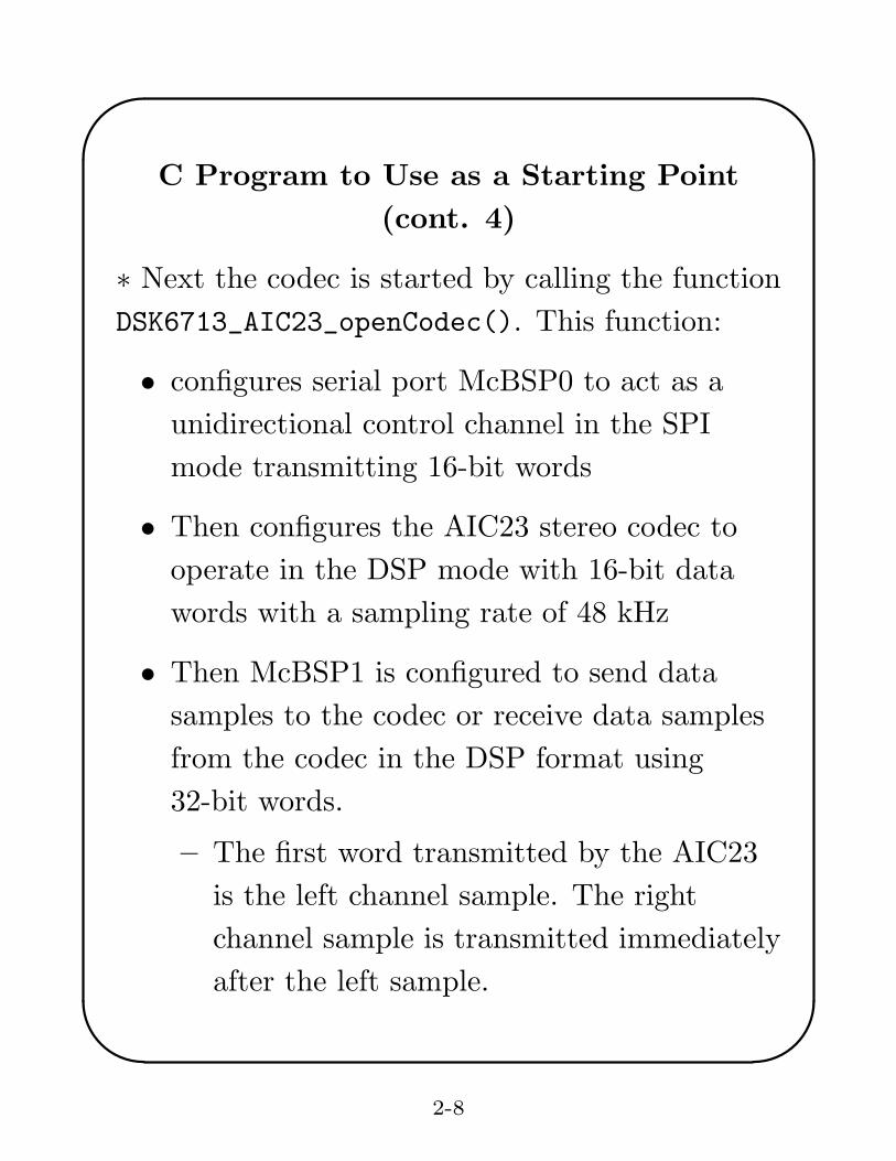
C Program to Use as a Starting Point
(cont. 4)
∗ Next the codec is started by calling the function
DSK6713_AIC23_openCodec(). This function:
• configures serial port McBSP0 to act as a
unidirectional control channel in the SPI
mode transmitting 16-bit words
• Then configures the AIC23 stereo codec to
operate in the DSP mode with 16-bit data
words with a sampling rate of 48 kHz
• Then McBSP1 is configured to send data
samples to the codec or receive data samples
from the codec in the DSP format using
32-bit words.
– The first word transmitted by the AIC23
is the left channel sample. The right
channel sample is transmitted immediately
after the left sample.
2-8

✬
✫
✩
✪
C Program to Use as a Starting
Point (cont. 5)
– The AIC23 generates a single frame sync
at the beginning of the left channel
sample. Therefore, a 32-bit word received
by McBSP1 contains the left sample in the
upper 16 bits and the right sample in the
lower 16 bits.
– The 16-bit samples are in 2’s complement
format.
– Words transmitted from McBSP1 to
AIC23 must have the same format.
– The codec and McBSP1 are configured so
that the codec generates the frame syncs
and shift clocks.
∗ See the text at the top of dskstart32.c for more details
about the UMD modifications of
DSK6713_AIC23_openCodec.c from the TI BSL version
which sets McBSP1 to transmit and receive 16-bit words.
2-9

✬
✫
✩
✪
C Program to Use as a Starting Point
(cont. 6)
∗ Finally, dskstart.c enters an infinite loop that
reads pairs of left and right channel samples from
the codec ADC and loops them back out to the
codec DAC. This loop should be replaced by the
C code to achieve the goals of your experiments.
/* Program dskstart32.c */
/***************************************************/
/* Program: dskstart32.c
This program can be used as a starting point for
writing DSK6713 applications. It contains the code
necessary to initialize the DSK board, TMS320C6713,
and AIC_23 codec.
****************************************************/
#include <stdio.h>
#include <stdlib.h>
#include <dsk6713.h>
#include <dsk6713_aic23.h>
#include <DSKintr.h>
#include <math.h>
2-10

✬
✫
✩
✪
C Program to Use as a Starting Point (cont. 7)
/* Codec configuration settings
See dsk6713_aic23.h and the TLV320AIC23 Stereo
Audio CODEC Data Manual for a details of the bits
in each of the 10 AIC23 control registers in the
following configuration structure. */
DSK6713_AIC23_Config config = { \
0x0017, /* 0 DSK6713_AIC23_LEFTINVOL
Left line input channel volume */ \
0x0017, /* 1 DSK6713_AIC23_RIGHTINVOL
Right line input channel volume */\
0x00d8, /* 2 DSK6713_AIC23_LEFTHPVOL
Left channel headphone volume */ \
0x00d8, /* 3 DSK6713_AIC23_RIGHTHPVOL
Right channel headphone volume */ \
0x0011, /* 4 DSK6713_AIC23_ANAPATH
Analog audio path control */ \
0x0000, /* 5 DSK6713_AIC23_DIGPATH
Digital audio path control */ \
0x0000, /* 6 DSK6713_AIC23_POWERDOWN
Power down control */ \
0x0043, /* 7 DSK6713_AIC23_DIGIF
Digital audio interface format */ \
0x0081, /* 8 DSK6713_AIC23_SAMPLERATE
Sample rate control (48 kHz) */ \
0x0001 /* 9 DSK6713_AIC23_DIGACT
Digital interface activation */ \};
2-11

✬
✫
✩
✪
C Program to Use as a Starting Point (cont. 8)
void main(void){
DSK6713_AIC23_CodecHandle hCodec;
Uint32 sample_pair = 0;
/* Initialize the interrupt system */
intr_reset();
/* dsk6713_init() must be called before other BSL
functions */
DSK6713_init(); /* In the BSL library */
/* Start the codec */
hCodec = DSK6713_AIC23_openCodec(0, &config);
/* Change the sampling rate to 16 kHz */
DSK6713_AIC23_setFreq(hCodec,
DSK6713_AIC23_FREQ_16KHZ);
/* Read left and right channel samples from the ADC
and loop them back out to the DAC.
Replace the following infinite loop with your code.*/
for(;;){
while(!DSK6713_AIC23_read(hCodec, &sample_pair));
while(!DSK6713_AIC23_write(hCodec, sample_pair));
}
}
2-12

✬
✫
✩
✪
Getting Samples to and from the
Codec
Sending Samples to the Codec
• Left and right sample pairs are sent to the
codec as 32-bit words with the left channel
sample in the upper 16 bits and the right
channel sample in the lower 16 bits. Each
sample is in 16-bit two’s complement format.
• These 32-bit words are sent to the codec by
the BSL function DSK6713_AIC23_write().
This function:
– polls the McBSP1 XRDY flag and returns
immediately without sending the sample if
it is false and also returns the value 0.
– It sends the sample word by writing it to
the Data Transmit Register (DXR) of
McBSP1 if XRDY is 1 (TRUE) and
returns the value 1.
2-13

✬
✫
✩
✪
The Function DSK6713 AIC23 write()
#include <dsk6713.h>
#include <dsk6713_aic23.h>
Int16 DSK6713_AIC23_write(DSK6713_AIC23_CodecHandle
hCodec, Uint32 val)
{ /* If McBSP not ready for new data, return false */
if (!MCBSP_xrdy(DSK6713_AIC23_DATAHANDLE)) {
return (FALSE);
}
/* Write 32 bit data value to DXR */
MCBSP_write(DSK6713_AIC23_DATAHANDLE, val);
/* Short delay for McBSP state machine to update */
asm(" nop");
asm(" nop");
asm(" nop");
asm(" nop");
asm(" nop");
asm(" nop");
asm(" nop");
asm(" nop");
return(TRUE);
}
Note: McBSP_xrdy() and MCBSP_write() are in
TI’s CSL library.
2-14

✬
✫
✩
✪
Receiving Samples from the Codec
Words are read from the codec by using the function
DSK6713_AIC23_read(). This function:
• polls the RRDY flag of McBSP1 and returns
immediately if it is FALSE without reading a
word and also returns the value FALSE.
• If RRDY is TRUE it reads a word from the Data
Receive Register (DRR) of McBSP1 and returns
the value TRUE.
Function DSK6713 AIC23 read.c
#include <dsk6713.h>
#include <dsk6713_aic23.h>
Int16 DSK6713_AIC23_read(DSK6713_AIC23_CodecHandle
hCodec, Uint32 *val)
{/* If no new data available, return false */
if (!MCBSP_rrdy(DSK6713_AIC23_DATAHANDLE)) {
return (FALSE);
}
/* Read the data */
*val = MCBSP_read(DSK6713_AIC23_DATAHANDLE);
return (TRUE);
}
Note: MCBSP_rrdy() and MCBSP_read() are in TI’s
CSL library.
2-15

✬
✫
✩
✪
AIC23 Properties
For complete details on the AIC23 Codec see:
Texas Instruments, “TLV320AIC23 Stereo Audio
CODEC Data Manual,” SLWS106C, July 2001.
AIC32 Sampling Rates
The C6713 DSK supplies a 12 MHz clock to the
AIC23 codec which is divided down internally in the
AIC23 to give the sampling rates shown in the table
below. The codec can be set to these sampling rates
by using the function
DSK6713_AIC23_setFreq(handle, freq ID).
freq ID Value Frequency
DSK6713 AIC23 FREQ 8KHZ 0x06 8000 Hz
DSK6713 AIC23 FREQ 16KHZ 0x2c 16000 Hz
DSK6713 AIC23 FREQ 24KHZ 0x20 24000 Hz
DSK6713 AIC23 FREQ 32KHZ 0x0c 32000 Hz
DSK6713 AIC23 FREQ 44KHZ 0x11 44100 Hz
DSK6713 AIC23 FREQ 48KHZ 0x00 48000 Hz
DSK6713 AIC23 FREQ 96KHZ 0x0e 96000 Hz
“Value” is put in AIC23 control register 8.
2-16

✬
✫
✩
✪
AIC23 Analog Interface Properties
• Line Inputs
ADC full-scale range of 1.0 V RMS
• Microphone Input
MICIN is a high-impedance, low-capacitance
input compatible with a wide range of
microphones.
• Line Outputs
DAC full-scale output voltage is 1.0 V RMS.
• Headphone Output
Stereo headphone outputs designed to drive
16 or 32-ohm headphones.
• Analog Bypass Mode
The analog line inputs can be directly
connected to the analog line outputs.
• Sidetone Interface
The AIC23 has a sidetone insertion mode
where the microphone input is routed to the
line and headphone outputs.
2-17

✬
✫
✩
✪
–70
–900 0.5 1 1.5
–50
–10
10
2 2.5 3
–30
Filt
er R
espo
nse
– dB
Normalized Audio Sampling Frequency
FILTER RESPONSEvs
NORMALIZED AUDIO SAMPLING FREQUENCY
Figure 3–11. ADC Digital Filter Response I: TI DSP and Normal Modes(Group Delay = 12 Output Samples)
–900 0.5 1 1.5
10
2 2.5 3
–10
–30
–50
–70
Filt
er R
espo
nse
– dB
Normalized Audio Sampling Frequency
FILTER RESPONSEvs
NORMALIZED AUDIO SAMPLING FREQUENCY
Figure 3–19. DAC Digital Filter Response I: TI DSP and Normal Modes
Note: NORMALIZED AUDIO SAMPLING FREQUENCY = f/fs
2-18

✬
✫
✩
✪
Creating a CCS Project for
dskstart32.c
• The first time you start CCS the “Workspace
Launcher” window will appear. It will
continue to appear each time you start CCS
until you check the “Use this as the default
and do not ask again” box. Enter the path to
your shared folder on the ECE Labs server
and check the box. You can change your
default workspace by clicking on “File →
Switch Workspace → Other” and the
“Workspace Launcher” will appear again.
• Now create a new project by clicking on
“Project” and then “New CCS Project.”
1. Enter (without quotes here and in the
future) “FirstProject” in the “Project
name:” box.
2-19
✬
✫
✩
✪
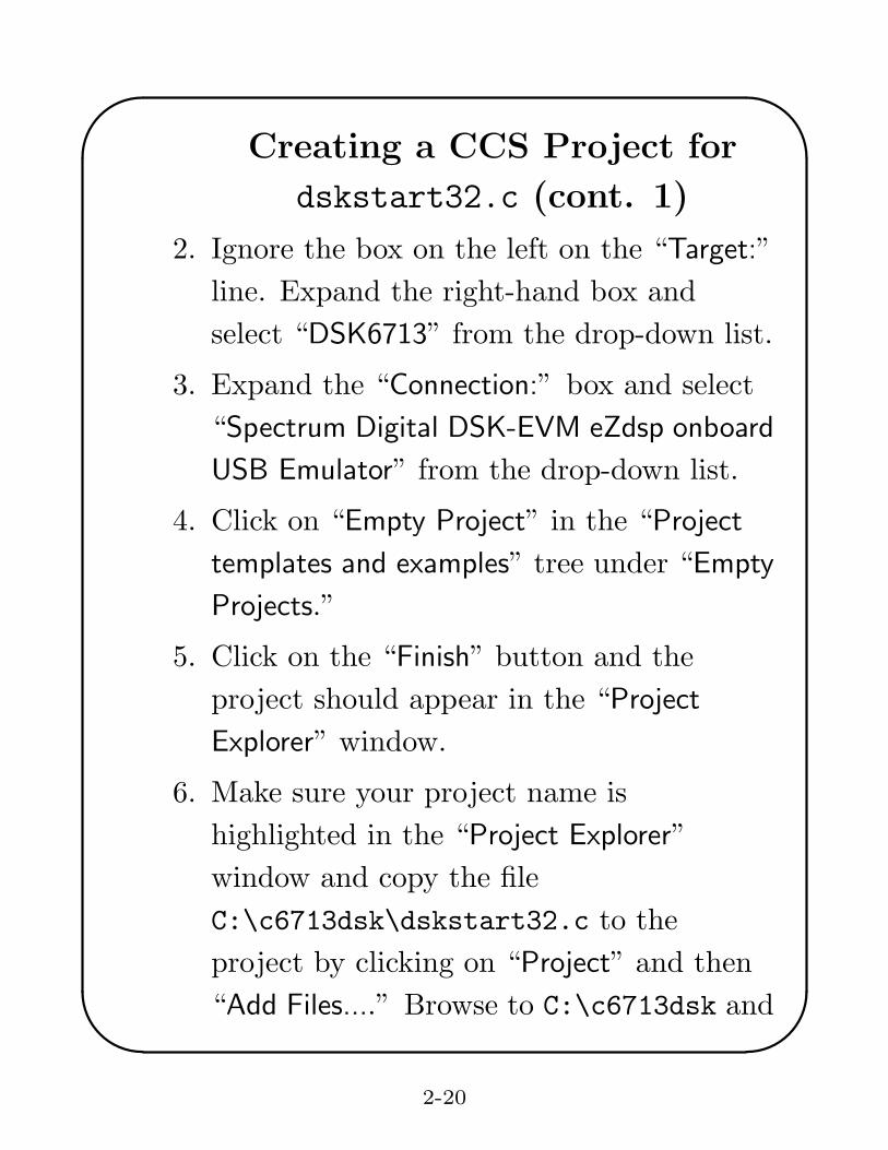
Creating a CCS Project for
dskstart32.c (cont. 1)
2. Ignore the box on the left on the “Target:”
line. Expand the right-hand box and
select “DSK6713” from the drop-down list.
3. Expand the “Connection:” box and select
“Spectrum Digital DSK-EVM eZdsp onboard
USB Emulator” from the drop-down list.
4. Click on “Empty Project” in the “Project
templates and examples” tree under “Empty
Projects.”
5. Click on the “Finish” button and the
project should appear in the “Project
Explorer” window.
6. Make sure your project name is
highlighted in the “Project Explorer”
window and copy the file
C:\c6713dsk\dskstart32.c to the
project by clicking on “Project” and then
“Add Files....” Browse to C:\c6713dsk and
2-20

✬
✫
✩
✪
Creating a CCS Project for
dskstart32.c (cont. 2)
select dskstart32.c. Select “Copy files”
rather than “Link to files” and click on the
OK button. dskstart32.c should appear
under your project in the “Project
Explorer” window. Double click on it to
show it in the editor window.
Project Build Options for Code Composer
Now build options for your project must be set.
Right click on the project name in the “Project
Explorer” window and then select “Show Build
Settings...” (Alternatively, you can first left click
on the project name to highlight it. Then left
click on “Project” and then “Show Build
Settings.”) Expand the “C6000 Compiler” menu in
the “Properties for FirstProject” window that
appears.
2-21

✬
✫
✩
✪
Project Build Options for CCS (cont. 1)
1. Select “Processor Options” and make sure
“Configuration:” is “Debug [Active]”
Set “Target processor version” to “6713”
2. Leave “Optimization” at its default.
3. Click on “Debug Option” and make sure the
“Debugging model” is “Full symbolic debug”
4. Expand “Advanced Options,” select
“Command Files,” and on the right after
“Read options ...” click on the icon of the
page with the green plus sign. In the “Add file
path” window enter
C:\c6713dsk\compiler.cmd and click on
“OK”. This file contains the include search
path directives:
-I="C:\c6713dsk\dsk6713bsl32\include"
-I="c:\Program Files\C6xCSL\include"
5. Select “Directory Specifier” and change any of
the paths to the ones you need.
2-22

✬
✫
✩
✪
Project Build Options for CCS (cont. 2)
6. Select “Predefined Symbols.” In the
“Pre-define NAME” box, click on the icon
with the green plus sign and enter:
CHIP_6713
This is used by the Chip Support Library
(CSL).
7. Skip “Include Options.”
8. Expand the “C6000 Linker” menu and select
“Basic Options.” Accept the default entries or
change them to your preferences.
9. Select “File Search Path” in the linker menu.
In the “Include library file or command file as
input (-library, -l)” window, click on the page
with a green plus sign icon and enter:
C:\c6713dsk\dsk6713.cmd
2-23

✬
✫
✩
✪
Project Build Options for CCS (cont. 3)
This linker command file contains the paths
and names of the libraries needed for your
ENEE 428 projects. It also defines the
memory map and code sections.
10. Expand the linker “Advanced Options”. Select
“Runtime Environment” and make sure the
“Initialization Model” is “Link using ROM
autoinitialization model (-rom model, -c).”
11. Click on the OK button to save the build
options and close the window.
A Simple First Experiment
• When the project has been created, build the
executable module by clicking on “Project”
and then “Build Project.” The “hammer” tool
bar icon also builds the project. At this point
you should correct any errors in your source
code or project.
2-24

✬
✫
✩
✪
A Simple First Experiment (cont. 1)
• You can have CCS build, load the .out file
into the DSK, and start it running in a debug
session by clicking on the little green bug icon
in the top menu bar.
The program, dskstart32.c, simply loops the
ADC input back to the DAC output. Check this
by doing the following:
• Plug a stereo cable into the DSK Line Input
and connect both channels to the same signal
generator output. The program dskstart32
sets the codec to sample at 16000 Hz, so set
the signal generator to output a sine wave of
less than 8000 Hz.
• Plug a stereo cable into the DSK Line
Output. Connect the left and right outputs
to two different oscilloscope channels.
NOTE: The right channel is the white plug
and the left channel is the red plug.
2-25
✬
✫
✩
✪
A Simple First Experiment (cont. 2)
• Start the program running by clicking on the
green bug in the top tool bar and wait for the
“Debug” window to appear. The program will
be loaded and run to main(void). Press the
green right “resume” arrow in the “Debug”
window or press F8 to continue program
execution and you should see the indication
that it is “(Running)” in the window.
Check that the sine waves appear on the
scope. Make sure the input level is small
enough so that there is no clipping.
• You can halt the program by clicking on the
yellow vertical parallel lines in the “Debug”
window tool bar. You can terminate the
debug session by clicking of the red square in
the tool bar. Run the cursor over the icons in
the tool bar to see what they do. You can
also click on “Run” in the top tool bar to see
a menu of all the debug icons and options.
2-26
✬
✫
✩
✪
A Simple First Experiment (cont. 3)
• Vary the sine wave frequency. What happens
when it is more than 8000 Hz? Why?
• Measure the amplitude response of the system
by varying the input frequency and dividing
the output amplitude by the input amplitude.
Make sure to include some frequencies
between 0 and 200 Hz.(Note: The signal
input and output paths contain blocking
capacitors so no DC is passed.) Plot the
amplitude response. Use enough frequencies
to get a smooth curve, particularly in regions
where the amplitude response changes
quickly. Your amplitude response results will
be needed for Chapter 3 experiments.
2-27

✬
✫
✩
✪
Multichannel Buffered Serial Port
(McBSP) Properties
• Can generate shift clocks and frame sync
signals internally, or use external signals (The
DSK uses external ones)
• Can transmit or receive 8, 12, 16, 20, 24, or
32-bit words
• Double-buffered data registers, which allow a
continuous data stream
• Can generate receive and transmit interrupts
to the CPU or events to the EDMA
• µ-law and A-law hardware companding
options
• Multichannel selection of up to 32 elements
from a 128 element TDMA frame
• Direct interface to industry-standard codecs
2-28

✬
✫
✩
✪
McBSP Block Diagram
'C6000 McBSP
Transmit ter
Receiver
Samp leRate Gen.
Events/Interrupts
D X
FSX
D R
FSR
CLKX
CLKR
CLKS
CPUclk FSG
CLKG
XEVT
REVT
XINT
RINT
To DMA To CPU
DX/DR Serial transmit/receive data
FSX/FSR Transmit/receive frame sync
CLKX/CLKR Transmit/receive serial shift clock
XINT/RINT Transmit/receive interrupt to CPU
XEVT/REVT Transmit/receive interrupt to DMA
CLKS External clock for Sample Rate Gen.
Shaku Anjanaiah and Brad Cobb, “TMS320C6000 McBSP
Initialization,” SPRA488A, September 2001, Figure 1, p. 2.
2-29

✬
✫
✩
✪
McBSP Transmitter Block Diagram
DXRData Transmit Register(018C0004h)
Transmit ShiftRegister Transmit Data
DX pin
XSR
32
1
32
Serial Port Control Register (018C0008h)
21 20 1
RRSTRRDYRINTM RFULLRJUSTXRSTXRDYXINTM
0214 13
XEMPTY
161718 5 4
Note: Addresses are for McBSP0
2-30

✬
✫
✩
✪
Operation of Serial Port Transmitter
• The CPU or EDMA writes a word into the
Data Transmit Register (DXR). The XRDY
flag is cleared whenever data is written to the
DXR.
• After a word (32 bits in our case) is shifted
out of Transmit Shift Register (XSR), a
parallel transfer of the DXR into the XSR is
performed. The XRDY flag is set when the
transfer occurs.
• The serial port transmitter sends an interrupt
request (XINT) to the CPU when the XRDY
flag makes a transition from 0 to 1 if XINTM
= 00b in the SPCR. It also sends a Transmit
Event Notice (XEVT) to the EDMA.
2-31

✬
✫
✩
✪
McBSP Receiver Block Diagram
DRRData Receive Register(018C0000h)
Receive ShiftRegister Receive Data
DR pin
RSR
32
32
1
RBR
32
Receive BufferRegister
Note: Addresses are for McBSP0
2-32

✬
✫
✩
✪
Operation of Serial Port Receiver
• RX bits shift serially into the Receive Shift
Register (RSR).
• When a full element is received, the 32-bit
RSR is transferred in parallel to the Receive
Buffer Register (RBR) if it is empty.
• The RBR is copied to the Data Receive
Register (DRR) if it is empty.
• The RRDY bit in SPCR is set to 1 when
RSR is moved to DRR, and it is cleared when
DRR is read.
• When RRDY transitions from 0 to 1, the
McBSP generates a CPU interrupt request
(RINT) if RINTM = 00b in the SPCR. A
receive event (REVT) is also sent to the
EDMA controller.
2-33

✬
✫
✩
✪
Example C Code for Polling Stereo Read
DSK6713_AIC23_CodecHandle hCodec;
Uint32 sample_pair = 0;
float left, right;
...
/* Read input sample pair using the polling BSL
McBSP read function */
while(!DSK6713_AIC23_read(hCodec,&sample_pair));
/* Shift right to move left ch 16 bits to
bits 15 - 0 and extended sign into
bits 31 - 16. Then convert to float. Since
sample_pair is an unsigned 32-bit int it
must be cast into a 32-bit signed int for an
arithmetic right shift with sign extension */
left = ( (int) sample_pair) >> 16;
/* Shift left by 16 to lop off left ch and
then right by 16 to sign extend.
Convert to float. */
right =( (int) sample_pair) << 16 >> 16;
2-34

✬
✫
✩
✪
Example C Code for Polling Stereo
Write
DSK6713_AIC23_CodecHandle hCodec;
float left, right;
int ileft, iright, sample;
...
/* Convert left and right values to integers */
ileft = (int) left;
iright = (int) right;
/* Combine L/R samples into a 32-bit word */
sample = (ileft<<16)|(iright & 0x0000FFFF);
/* Poll XRDY bit until true, then write to DXR*/
while(!DSK6713_AIC23_write(hCodec, sample));
2-35

✬
✫
✩
✪
Chapter 2, Experiment 2Generating Sine Waves Using XRDY
Polling
For Experiment 2.2, do the following:
1. Initialize the codec as in dskstart32.c.
2. Set the sampling rate to 16 kHz.
3. Generate a 1 kHz sine wave on the left
channel and a 2 kHz sine wave on the right
channel. Remember that | sin(x)| ≤ 1 and
that floats less than 1 become 0 when
converted to ints. Therefore, scale your
floating point sine wave samples to make
them greater than 1 and fill reasonable part
of the DAC dynamic range before converting
them to ints.
4. Combine the left and right channel integer
samples into a 32-bit integer and write the
resulting word to the McBSP1 DXR using
polling of the XRDY flag.
2-36

✬
✫
✩
✪
Experiment 2.2 (cont.)
5. Observe the left and right channel outputs on
two oscilloscope channels.
6. Verify that the sine wave frequencies observed
on the scope are the desired values by
measuring their periods.
7. Use the counter in the signal generator or the
frequency function of the oscilloscope to
measure the frequencies.
8. When you have verified that your program is
working, change the left channel frequency to
15 kHz and the right channel frequency to 14
kHz. Measure the DAC output frequencies.
Explain your results mathematically with
equations. (Hint: Look up “aliasing” in any
reference on digital signal processing.)
2-37

✬
✫
✩
✪
Generating Samples of a Sine Wave
Continuous Time Sine Wave
s(t) = sin 2πf0t
Sampled Sine Wave
Let fs = 1/T be the sampling rate where T is the
sampling period.
s(nT ) = sin 2πf0nT = sin 2πf0fs
n
= sinn∆θ
where ∆θ = 2πf0/fs
Recursive Angle Generation
Let
θ(n) = n∆θ
Then
θ(n+ 1) = (n+ 1)∆θ = n∆θ +∆θ = θ(n) + ∆θ
2-38

✬
✫
✩
✪
Sample Program Segment for Polling
#include <math.h>
#define pi 3.141592653589
#define fs 16000.
#define f0 1000.
float delta = 2.*pi*f0/fs;
float twopi = 2.0*pi;
float angle = 0;
float left;
int sample = 0;
for(;;){ /* Infinite loop */
left = 15000.0*sin(angle); /* Scale for DAC */
sample = ((int) left) <<16;/* Put in top half*/
/* Poll XRDY bit until true, then write to DXR*/
while(!DSK6713_AIC23_write(hCodec, sample));
angle += delta; /* Increment sine wave angle */
if( angle >= twopi) angle -= twopi;
/* Keep angle from overflowing */
}
2-39

✬
✫
✩
✪
Some Important Information
• Remember to include math.h in your C
program.
• The DSK has stereo LINE IN and LINE
OUT jacks. The lab has cables to convert
from the DSK stereo plug to an RCA mono
connector for the left channel and an RCA
mono connector for the right channel. The
RCA connectors are plugged into RCA to
BNC adapters so they can be connected to
the oscillators and oscilloscopes.
• Cable Color Scheme
– Left Channel: Red plug
– Right Channel: White plug
2-40

✬
✫
✩
✪
Method 2 for Generating a Sine
Wave – Using Interrupts
Almost all the time in the polling method is spent
sitting in a loop waiting for the XRDY flag to get
set. A much more efficient approach is to let the
DSP perform all sorts of desired tasks in the
background and have the serial port interrupt
these background tasks when it needs a sample to
transmit. The interrupt service routine is called a
foreground task.
The TMS320C6713 contains a vectored priority
interrupt controller.
• The highest priority interrupt is RESET
which cannot be masked.
• The next priority interrupt is the
Non-Maskable Interrupt (NMI) which is used
to alert the DSP of a serious hardware
problem.
2-41
✬
✫
✩
✪
Using Interrupts (cont. 1)
• There are two reserved interrupts and 12
additional maskable CPU interrupts. The
peripherals, such as, the timers, McBSP and
McASP serial ports, EDMA controller, plus
external interrupt pins sourced from the
GPIO module present a set of many interrupt
sources. The 16 CPU interrupts and their
default sources are shown in the table on
Slide 2-43. INT 00 has the highest priority
and INT 15 the lowest.
• The interrupt system includes a multiplexer
to select the CPU interrupt sources and map
them to the 12 maskable prioritized CPU
interrupts. The complete list of C6713
interrupt sources is shown in the tables on
Slides 2-44 and 2-45 along with the required
Interrupt Selector values.
• The GPIO module can select external pins as
interrupt sources. The mapping is shown of
Slide 2-46.
2-42

TMS320C6713 Default Interrupt Source
Mapping
INTERRUPT DEFAULTCPU SELECTOR SELECTOR DEFAULT
INTERRUPT CONTROL VALUE INTERRUPTNUMBER REGISTER (BINARY) EVENT
INT 00 - - RESET
INT 01 - - NMI
INT 02 - - Reserved
INT 03 - - Reserved
INT 04 MUXL[4:0] 00100 GPINT4
INT 05 MUXL[9:5] 00101 GPINT5
INT 06 MUXL[14:10] 00110 GPINT6
INT 07 MUXL[20:16] 00111 GPINT7
INT 08 MUXL[25:21] 01000 EDMAINT
INT 09 MUXL30:26] 01001 EMUDTDMA
INT 10 MUXH[4:0] 00011 SDINT
INT 11 MUXH[9:5] 01010 EMURTDXRX
INT 12 MUXH[14:10] 01011 EMURTDXTX
INT 13 MUXH[20:16] 00000 DSPINT
INT 14 MUXH[25:21] 00001 TINT0
INT 15 MUXH[30:26] 00010 TINT1
2-43

✬
✫
✩
✪
First 16 Interrupt Sources
INTERRUPTSELECTOR INTERRUPT MODULE
VALUE EVENT(BINARY)
00000 DSPINT HPI
00001 TINT0 Timer 0
00010 TINT1 Timer 1
00011 SDINT EMIF
00100 GPINT4 GPIO
00101 GPINT5 GPIO
00110 GPINT6 GPIO
00111 GPINT7 GPIO
01000 EDMAINT EDMA
01001 EMUDTDMA Emulation
01010 EMURTDXRX Emulation
01011 EMURTDXTX Emulation
01100 XINT0 McBSP0
01101 RINT0 McBSP0
01110 XINT1 McBSP1
01111 RINT1 McBSP1
2-44

✬
✫
✩
✪
Remaining 16 Interrupt Sources
INTERRUPTSELECTOR INTERRUPT MODULE
VALUE EVENT(BINARY)
10000 GPINT0 GPIO
10001 Reserved -
10010 Reserved -
10011 Reserved -
10100 Reserved -
10101 Reserved -
10110 I2CINT0 I2C0
10111 I2CINT1 I2C1
11000 Reserved -
11001 Reserved -
11010 Reserved -
11011 Reserved -
11100 AXINT0 McASP0
11101 ARINT0 McASP0
11110 AXINT1 McASP1
11111 ARINT1 McASP1
2-45

✬
✫
✩
✪
External Interrupt Sources
PIN INTERRUPT MODULE
NAME EVENT
GP[15] GPINT0 GPIO
GP[14] GPINT0 GPIO
GP[13] GPINT0 GPIO
GP[12] GPINT0 GPIO
GP[11] GPINT0 GPIO
GP[10] GPINT0 GPIO
GP[9] GPINT0 GPIO
GP[8] GPINT0 GPIO
GP[7] GPINT0 or GPINT7 GPIO
GP[6] GPINT0 or GPINT6 GPIO
GP[5] GPINT0 or GPINT5 GPIO
GP[4] GPINT0 or GPINT4 GPIO
GP[3] GPINT0 GPIO
GP[2] GPINT0 GPIO
GP[1] GPINT0 GPIO
GP[0] GPINT0 GPIO
2-46

Interrupt Control Registers
Name Description
CSR Control status
register
Globally set or disable
interrupts
IER Int enable reg Enable interrupts. Bit
n corresponds to INT n
IFR Int flag regis-
ter
Shows status of inter-
rupts. Bit n corre-
sponds to INT n
ISR Interrupt set
register
Manually set flags in
IFR
ICR Interrupt clear
register
Manually clear flags in
IFR
ISTP Interrupt
service table
pointer
Pointer to the begin-
ning of the interrupt
service table
NRP Nonmaskable
interrupt
return pointer
Return address used on
return from a nonmask-
able interrupt
IRP Interrupt
return pointer
Return address used on
return from a maskable
interrupt
2-47

✬
✫
✩
✪
Conditions for an Interrupt
The following conditions must be met to process
a maskable interrupt:
• The global interrupt enable bit (GIE) which is
bit 0 in the control status register (CSR) is
set to 1. When GIE = 0, no maskable
interrupt can occur.
• The NMIE bit in the interrupt enable register
(IER) is set to 1. No maskable interrupt can
occur if NMIE = 0.
• The bit corresponding to the desired
interrupt is set to 1 in the IER.
• The desired interrupt occurs, which sets the
corresponding bit in the interrupt flags
register (IFR) to 1 and no higher priority
interrupt flags are 1 in the IFR
2-48
✬
✫
✩
✪
What Happens When an Interrupt
Occurs
• The corresponding flag bit in the IFR is set to 1.
• If GIE = NMIE = 1 and no higher priority
interrupts are pending, the interrupt is serviced:
– GIE is copied to PGIE and GIE is cleared to
preclude other interrupts.
– The flag bit in the IFR is cleared.
– The return address is put in the interrupt
return pointer (IRP).
– When CPU interrupt INT n occurs, program
execution jumps to byte offset 4× 8× n = 32n
in an interrupt service table (IST).
∗ The IST contains 16 interrupt service fetch
packets (ISFP), each consisting of eight
32-bit instruction words.
2-49

✬
✫
✩
✪
What Happens When an Interrupt
Occurs (cont.)
∗ An ISFP may contain an entire interrupt
service routine or may branch to a larger
service routine.
∗ We will normally start the interrupt service
table (IST) at location 0. It can be relocated
and the Interrupt Service Table Pointer
register (ISTP) points to its starting address
which must be a multiple of 256 words.
– The service routine must save the CPU state
on entry and restore it on exit.
– A return from a maskable interrupt is
accomplished by the assembly instructions
B IRP; return, moves PGIE to GIE
NOP 5 ; delay slots for branch
2-50

✬
✫
✩
✪
Example of an Interrupt Service
Fetch Packet
An ISFP for RESET for C programs is shown
below.
mvkl _c_int00, b0; load lower 16 bits of _c_init
mvkh _c_int00, b0; load upper 16 bits of _c_init
b b0 ; branch to C initialization
;
; Note: 5 instructions are executed before the
; branch actually occurs.
;;;;;;;;;;;;;;;;;;;;;;;;;;;;;;;;;;;;;;;;;;;;;;;
mvc PCE1, b0 ; get base of IST
mvc b0, ISTP ; load pointer to IST base
nop 3 ; do 3 NOP’s to make a total of
; 5 instructions after branch
;;;;;;;;;;;;;;;;;;;;;;;;;;;;;;;;;;;;;;;;;;;;;;;;
nop ; add two words to fetch packet
nop ; to make a total of 8 words
2-51
✬
✫
✩
✪
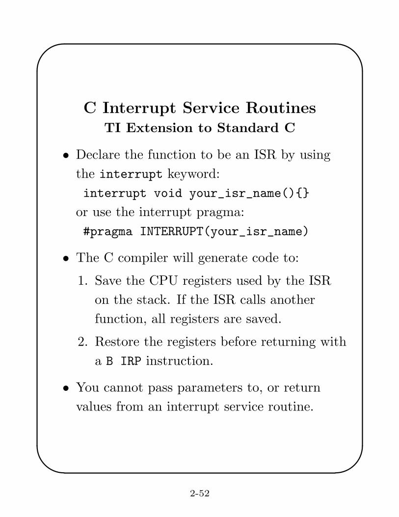
C Interrupt Service RoutinesTI Extension to Standard C
• Declare the function to be an ISR by using
the interrupt keyword:
interrupt void your_isr_name(){}
or use the interrupt pragma:
#pragma INTERRUPT(your_isr_name)
• The C compiler will generate code to:
1. Save the CPU registers used by the ISR
on the stack. If the ISR calls another
function, all registers are saved.
2. Restore the registers before returning with
a B IRP instruction.
• You cannot pass parameters to, or return
values from an interrupt service routine.
2-52

✬
✫
✩
✪
Using the dsk6713bsl32.lib Interrupt
Functions
To write and build programs using the TI C
interrupt extensions and the dsk6713bsl32
interrupt functions:
• Set the project build options as before.
• Include the following header file in your C
program
C:\c6713dsk\dsk6713bsl32\include\DSKintr.h
The include search path should already be set
in the project build options.
• The linker command file adds the library
dsk6713bsl32.lib to your project file.
• The interrupt service table is generated in a
section called .intvecs. The sample
beginning linker command file dsk6713.cmd
loads the .intvecs section starting at
absolute address 0.
2-53

Selected Library Interrupt Functions
INTR_CHECK_FLAG(bit) Returns value of bit in
IFR
INTR_CLR_FLAG(bit) Clears int by writing 1 to
ICR
INTR_ENABLE(bit) Sets bit in IER
INTR_DISABLE(bit) Clears bit in IER
INTR_GLOBAL_ENABLE(bit) Sets GIE bit in CSR
INTR_GLOBAL_DISABLE(bit) Clears GIE bit in CSR
intr_hook(*fp,cpu_intr) Place func ptr into isr
jump table at location
for cpu interrupt
intr_reset() Clears GIE, PGIE, IER,
and IFR; resets interrupt
select mux’s; initializes
IST and ISTP; installs
ISR Jump Table
intr_init() Initialize ISTP
intr_map(cpu_intr, isn) Maps int source to the
CPU interrupt
intr_isn(cpu_intr) Returns interrupt src
number for CPU inter-
rupt
2-54

✬
✫
✩
✪
Installing a C ISR
• Use intr_reset() to install the interrupt
service table and interrupt branch table, clear
GIE, and clear flags in IFR.
• Map the interrupt source number to a CPU
interrupt number.
intr_map(CPU_INT15, ISN_XINT0);
• Clear the interrupt flag to make sure none is
pending.
INTR_CLR_FLAG(CPU_INT15);
• Hook the ISR to the CPU interrupt. Let the
ISR be my_isr().
intr_hook(my_isr, CPU_INT15);
• Enable the NMI interrupt.
INTR_ENABLE(CPU_INT_NMI);
• Enable the CPU interrupt in the IE register.
INTR_ENABLE(CPU_INT15);
• Set the GIE bit in the CSR.
INTR_GLOBAL_ENABLE();
2-55

✬
✫
✩
✪
Chapter 2, Experiment 3Generating Sine Waves by Using Interrupts
Repeat the steps for Experiment 2.2 but now use
a C interrupt service routine to generate the sine
wave samples and write them to the McBSP1
data transmit register (DXR1). No polling of the
XRDY flag is needed because samples are
transmitted only when interrupts from the
McBSP1 transmitter cause execution to jump
into your interrupt service routine.
The main() function should:
• initialize McBSP0, McBSP1, and the codec
with a 16 kHz sampling rate
• map CPU INT15 to McBSP1 XINT1
Note: The choice of INT15 was arbitrary.
Any of INT4 – INT15 can be used.
• hook CPU INT15 to your ISR
• enable interrupts
• go into an infinte interruptable loop
2-56

✬
✫
✩
✪
Sample C Segment for Interrupts
#include <stdio.h>
#include <stdlib.h>
#include <dsk6713.h>
#include <dsk6713_aic23.h>
#include <DSKintr.h>
.
.
.
#define sampling_rate 16000.
#define freq_left 1000.
#define freq_right 2000.
#define scale 10000.0
#define PI 3.141592653589
float twopi = 2.*PI;
float delta_left = 2.0*PI*freq_left/sampling_rate;
/*phase increment left sine */
float delta_right = 2.0*PI*freq_right/sampling_rate;
/*phase increment right sine*/
interrupt void tx_isr(void); /* prototype the ISR */
2-57

✬
✫
✩
✪
Sample Program for Ints (cont. 1)
void main(void){
DSK6713_AIC23_CodecHandle hCodec;
/* Initialize interrupt system with intr_reset() */
/* */
/* The default interrupt service routines are */
/* set up by calling the function intr_reset() in */
/* the UMD added file intr.c. This clears GIE */
/* and PGIE, disables all interrupts except RESET */
/* in IER, clears the flags in the IFR for the */
/* the maskable interrupts INT4 - INT15, resets */
/* the interrupt multiplexers, initializes the */
/* interrupt service table pointer (ISTP), and */
/* sets up the Interrupt Service Routine Jump */
/* Table. */
intr_reset();
/* dsk6713_init() must be called before other */
/* BSL functions */
DSK6713_init(); /* In the BSL library */
/* Start the codec. McBSP1 uses 32-bit words */
hCodec = DSK6713_AIC23_openCodec(0, &config);
2-58

✬
✫
✩
✪
Sample Program for Ints (cont. 2)
/* Change the sampling rate to 16 kHz */
DSK6713_AIC23_setFreq(hCodec,
DSK6713_AIC23_FREQ_16KHZ);
/* Select McBSP1 transmit int for INT15 */
intr_map(CPU_INT15, ISN_XINT1);
/* Hook our ISR to INT15 */
intr_hook(tx_isr, CPU_INT15);
/* Clear old interrupts */
INTR_CLR_FLAG(CPU_INT15);
/* Enable interrupts */
/* NMI must be enabled for other ints to occur */
INTR_ENABLE(CPU_INT_NMI);
/* Set INT15 bit in IER */
INTR_ENABLE(CPU_INT15);
/* Turn on enabled ints */
INTR_GLOBAL_ENABLE();
/*Write a word to start transmission */
MCBSP_write(DSK6713_AIC23_DATAHANDLE, 0);
for (;;); /* infinite loop */
}
2-59

✬
✫
✩
✪
Sample Program for Ints (cont. 3)
interrupt void tx_isr(void){
float x_left, x_right;
/*************************************************/
/* Note: angle_left and angle_right must retain */
/* their values between ISR calls. This can be */
/* done by making them static as below or global.*/
/*************************************************/
static float angle_left=0.;
static float angle_right=0.;
int output, ileft, iright;
/* 1. Generate scaled left and right channel sine */
/* samples. Convert them to integers and combine */
/* into a 32-bit word, output. */
/* 2. Increment phase angles of sines modulo 2 pi.*/
/* 3. There is no need to poll XRDY since its */
/* transition from false to true causes a jump */
/* to this ISR. DSK6713_AIC23_DATAHANDLE is */
/* declared as a global variable in */
/* DSK6713_aic23_opencodec.c. Just write the */
/* output sample to McBSP1 by the CSL library */
/* function MCBSP_write as shown below. *.
MCBSP_write(DSK6713_AIC23_DATAHANDLE, output);
}
2-60

✬
✫
✩
✪
Enhanced Direct Memory Access
(EDMA)
The Enhanced Direct Memory Access Controller
(EDMA) handles all data transfers between the
L2 cache/memory controller and the peripherals.
These include cache servicing, non-cacheable
memory access, user-programmed data transfers,
and host access.
The EDMA can move data to and from any
addressable memory spaces including internal
memory (L2 SRAM), peripherals, and external
memory.
The EDMA is quite complex and we will only
touch on its operation. See TMS320C6000
Peripherals Reference Guide, SPRU190D,
Chapter 4 and TMS320C6713B Floating-Point
Digital Signal Processor, SPRS294B, October
2005 for complete details.
2-61

✬
✫
✩
✪
EDMA Overview
• The EDMA controller includes event and
interrupt processing registers, an event
encoder, a parameter RAM, and address
generation hardware.
• The EDMA has 16 independent channels and
they can be assigned priorities.
• Data transfers can be initiated by the CPU or
events.
• When an event occurs, its transfer parameters
are read from the Parameter RAM (PaRAM).
These parameters are sent to address
generation hardware.
• The EDMA can transfer elements that are
8-bit bytes, 16-bit halfwords, or 32-bit words.
• Very sophisticated block transfers can be
programmed. The EDMA can transfer
1-dimensional and 2-dimensional data blocks
consisting of multiple frames. (See
SPRU190D Section 6.8 for details.)
2-62

✬
✫
✩
✪
EDMA Overview (cont.)
• After an element transfer, source and/or
destination element addresses can stay the
same, be incremented or decremented by one
element, or incremented or decremented by
the value in the index register ELEIDX for the
channel. Arrays are offset by FRMIDX for the
channel.
• After a programmed transfer is completed,
the EDMA can continue data transfers by
linking to another transfer programmed in
the Parameter RAM for the channel or by
chaining to a transfer for another channel.
• The EDMA can generate transfer completion
interrupts to the CPU along with a
programable transfer complete code. The
CPU can then take some desired action based
on the transfer complete code.
• The EDMA has a quick DMA mode (QDMA)
that can be used for quick, one-time transfers.
2-63

✬
✫
✩
✪
EDMA Event Selection
The ’C6713 EDMA supports up to 16 EDMA
channels. Channels 8 through 11 are reserved for
chaining, leaving 12 channels to service peripheral
devices. Data transfers can be initiated by (1) the
CPU or (2) events. The default mapping of
events to channels is shown in Slide 2-66.
The user can change the mapping of events to
channels. The EDMA selector registers ESEL0,
ESEL1, and ESEL2 control this mapping. Slides
2-67, 2-68, and 2-69 show the events and selector
codes.
Registers for Event Processing
• Event Register (ER)
When event n occurs, bit n is set in the ER.
• Event Enable Register (EER)
Setting bit n of the EER enables processing of
that event. Setting bit n to 0 disables
processing of event n. The occurrence of event
n is latched in the ER even if it is disabled.
2-64

✬
✫
✩
✪
Registers for Event Processing
(cont.)
• Event Clear Register (ECR)
If an event is enabled in the EER and gets
posted in the ER, the ER bit is automatically
cleared when the EDMA processes the
transfer for the event. If the event is disabled,
the CPU can clear the event flag bit in the
ER by writing a 1 to the corresponding bit in
the ECR. Writing a 0 has no effect.
• Event Set Register (ESR)
Writing a 1 to a bit in the ESR causes the
corresponding bit in the event register (ER)
to get set. This allows the CPU to submit
event requests and can be used as a good
debugging tool.
2-65
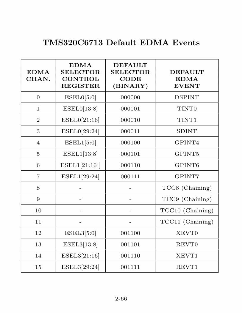
TMS320C6713 Default EDMA Events
EDMA DEFAULTEDMA SELECTOR SELECTOR DEFAULTCHAN. CONTROL CODE EDMA
REGISTER (BINARY) EVENT
0 ESEL0[5:0] 000000 DSPINT
1 ESEL0[13:8] 000001 TINT0
2 ESEL0[21:16] 000010 TINT1
3 ESEL0[29:24] 000011 SDINT
4 ESEL1[5:0] 000100 GPINT4
5 ESEL1[13:8] 000101 GPINT5
6 ESEL1[21:16 ] 000110 GPINT6
7 ESEL1[29:24] 000111 GPINT7
8 - - TCC8 (Chaining)
9 - - TCC9 (Chaining)
10 - - TCC10 (Chaining)
11 - - TCC11 (Chaining)
12 ESEL3[5:0] 001100 XEVT0
13 ESEL3[13:8] 001101 REVT0
14 ESEL3[21:16] 001110 XEVT1
15 ESEL3[29:24] 001111 REVT1
2-66
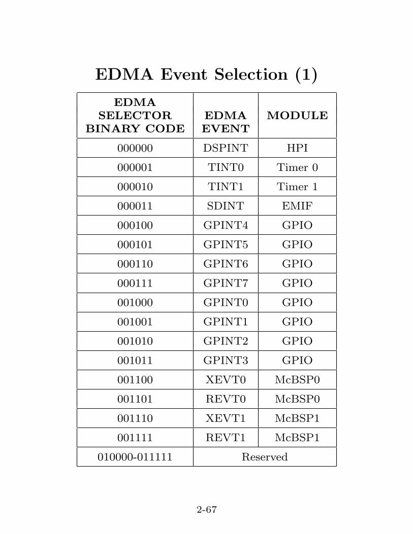
EDMA Event Selection (1)
EDMASELECTOR EDMA MODULE
BINARY CODE EVENT
000000 DSPINT HPI
000001 TINT0 Timer 0
000010 TINT1 Timer 1
000011 SDINT EMIF
000100 GPINT4 GPIO
000101 GPINT5 GPIO
000110 GPINT6 GPIO
000111 GPINT7 GPIO
001000 GPINT0 GPIO
001001 GPINT1 GPIO
001010 GPINT2 GPIO
001011 GPINT3 GPIO
001100 XEVT0 McBSP0
001101 REVT0 McBSP0
001110 XEVT1 McBSP1
001111 REVT1 McBSP1
010000-011111 Reserved
2-67

EDMA Event Selection (2)
EDMASELECTOR EDMA MODULE
BINARY CODE EVENT
100000 AXEVTE0 McASP0
100001 AXEVTO0 McASP0
100010 AXEVT0 McASP0
100011 AREVTE0 McASP0
100100 AREVTO0 McASP0
100101 AREVT0 McASP0
100110 AXEVTE1 McASP1
100111 AXEVTO1 McASP1
101000 AXEVT1 McASP1
101001 AREVTE1 McASP1
101010 AREVTO1 McASP1
101011 AREVT1 McASP1
2-68

EDMA Event Selection (3)
EDMASELECTOR EDMA MODULE
BINARY CODE EVENT
101100 I2CREVT0 I2C0
101101 I2CXEVT0 I2C0
101110 I2CREVT1 I2C1
101111 I2CXEVT1 I2C1
110000 GPINT8 GPIO
110001 GPINT9 GPIO
110010 GPINT10 GPIO
110011 GPINT11 GPIO
110100 GPINT12 GPIO
110101 GPINT13 GPIO
110110 GPINT14 GPIO
110111 GPINT15 GPIO
111000-111111 Reserved
2-69

The Parameter RAM (PaRAM)
The transfer parameter table for the EDMA
channels and link information is stored in the
Parameter RAM (PaRAM) which is a 2K-byte
RAM block located within the EDMA. The table
consists of six-word parameter sets for a total of
85 sets. Each set uses 6× 4 = 24 bytes and
contains the parameters for a transfer shown in
the following table.
Format of a Transfer Set Record
31 16 15 0
Options (OPT) Word 0
Source Address (SRC) Word 1
Array/frame count Element count Word 2
(FRMCNT) (ELECNT)
Destination Address (DST) Word 3
Array/frame index Element index Word 4
(FRMIDX) (ELEIDX)
Element count link address Word 5
reload (ELERLD) (LINK)
2-70
✬
✫
✩
✪
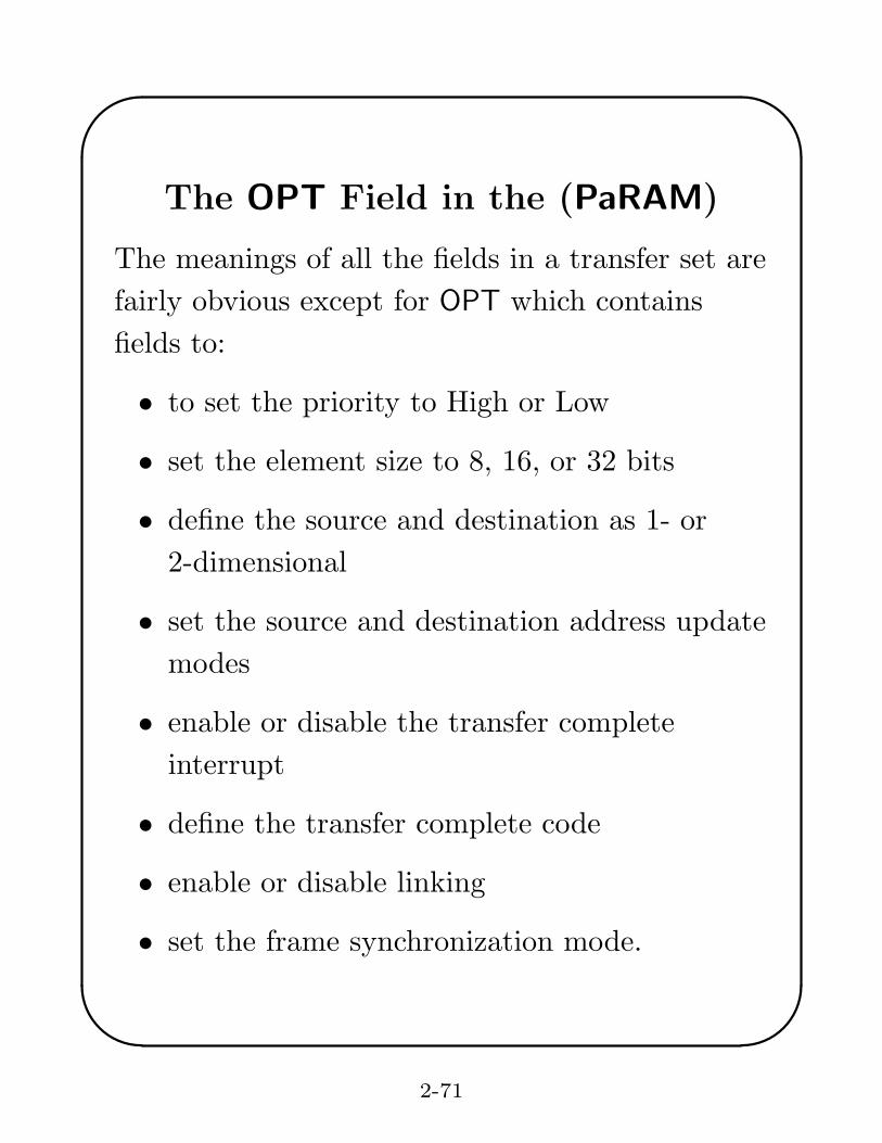
The OPT Field in the (PaRAM)
The meanings of all the fields in a transfer set are
fairly obvious except for OPT which contains
fields to:
• to set the priority to High or Low
• set the element size to 8, 16, or 32 bits
• define the source and destination as 1- or
2-dimensional
• set the source and destination address update
modes
• enable or disable the transfer complete
interrupt
• define the transfer complete code
• enable or disable linking
• set the frame synchronization mode.
2-71

✬
✫
✩
✪
Contents of the PaRAM
The PaRAM is organized as follows:
• The first 16 parameter sets are for the 16 EDMA
events. Each set contains 24 bytes.
• The remaining parameter sets are used for linking
transfers. Each set is 24 bytes.
• The remaining 8 bytes of unused RAM can be
used as a scratch pad area. A part of or the entire
PaRAM can be used as a scratch pad RAM when
the events corresponding to this region are
disabled.
When an event mapped to a particular channel
occurs, say channel n with n ∈ {0, 1, . . . , 15}, its
parameters are read from parameter set n in the
PaRAM and sent to the address generation hardware.
2-72

✬
✫
✩
✪
Synchronization of EDMA Transfers
The EDMA can make 1 or 2-dimensional
transfers. We will only consider the 1-D case. A
1-D block transfer consists of FRMCNT+ 1
frames. Each frame consists of the number of
elements specified by the field ELECNT in the
parameter set. The following two types of 1-D
synchronized transfers are possible:
1. Element Synchronized 1-D Transfer
(FS=0 in OPT)
When a channel sync event occurs, for
example, a transition of a McBSP XRDY flag
from false to true,
• an element in a frame is transferred from
its source to destination,
• The source and destination addresses are
updated in the parameter set after the
element is transferred,
• and the element count (ELECNT) is
decremented in the parameter set.
2-73

✬
✫
✩
✪
Synchronization of Transfers (cont.)
When ELCNT = 1, indicating the final element in
the frame, and a sync event occurs,
• the element is transferred.
• Then the element count is reloaded with the
value of ELERLD in the parameter set and
• the frame count (FRMCNT) is decremented
by 1.
• The EDMA continues transfers at sync events
for a new frame if one still remains to be
transferred.
2. Frame Synchronized 1-D Transfers
(FS = 1 in OPT )
A sync event causes all the elements in a
frame to be transferred as rapidly as possible.
Each new event causes another frame to be
transferred as rapidly as possible until the
requested number of frames has been
transferred.
2-74

✬
✫
✩
✪
Linking EDMA Transfers
• When the LINK field, bit 1, in options
parameter OPT is set to 0, the EDMA stops
after a transfer is completed.
• When LINK = 1 and the requested transfer is
completed, the transfer parameters are
reloaded with the parameter set pointed to by
the 16-bit link address, and the EDMA
continues transfers with this new set.
– The entire parameter RAM is located in
the memory area 01A0xxxxh, so a 16-bit
link address is sufficient. The link address
must be located on a 24-byte boundary.
– There is no limit to the number of
transfers that can be linked. However, the
final transfer should link to a NULL
parameter set which is one with all its
entries set to 0 (24 zero bytes).
2-75

✬
✫
✩
✪
Linking EDMA Transfers (cont.)
– A transfer can be linked to itself to
simulate the autoinitialization feature of
the TMS320C6201 and TMS320C6701
DMA. This is useful for circular buffering
and repetitive transfers.
– To eliminate timing problems resulting
from the parameter reload time, the event
register (ER) is not checked while the
parameters are being reloaded. However,
new events are registered in the ER.
– Any record in the PaRAM can be used for
linking. However, a set in the first 16
should be used only if the corresponding
event is disabled.
2-76

✬
✫
✩
✪
EDMA Interrupts to the CPU
When the TCINT bit is set to 1 in OPT for an
EDMA channel and the event mapped to the
channel occurs, the EDMA sets a bit in the
channel interrupt pending register (CIPR)
determined by the transfer complete code
programmed in OPT.
Then, if the bit corresponding to the channel is
set in the channel interrupt enable register
(CIER), the EDMA generates the interrupt
EDMA INT to the CPU.
If the CPU interrupt EDMA INT (default
CPU INT8) is enabled in the CPU IER, program
execution jumps to the vectored interrupt service
routine (ISR). The ISR can read the CIPR to
check which EDMA events have been registered
as completed and take the appropriate action.
2-77

✬
✫
✩
✪
Chaining EDMA Channels
The EDMA chaining capability allows the
completion of an EDMA channel transfer to
trigger another EDMA channel transfer. EDMA
chaining does not modify any channel parameters.
It just gives a synchronization event to the
chained channel.
Linking and chaining are different. Linking
reloads the current channel parameters with the
linked parameters and transfers continue on the
same channel with the linked parameters.
Chaining does not modify or update any chained
parameters. It simply gives a synchronization
event to the chained channel.
Channels 8, 9, 10, and 11 are reserved for
chaining. Chaining is enabled by setting bit 8, 9,
10, or 11 in the channel chain enable register
(CCER). The four-bit field, transfer complete code
(TCC), in OPT for a channel must also be set to
one of these four values to cause chaining to occur
at the end of the transfer.
2-78
✬
✫
✩
✪
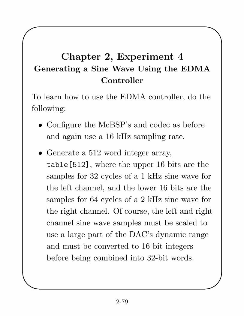
Chapter 2, Experiment 4Generating a Sine Wave Using the EDMA
Controller
To learn how to use the EDMA controller, do the
following:
• Configure the McBSP’s and codec as before
and again use a 16 kHz sampling rate.
• Generate a 512 word integer array,
table[512], where the upper 16 bits are the
samples for 32 cycles of a 1 kHz sine wave for
the left channel, and the lower 16 bits are the
samples for 64 cycles of a 2 kHz sine wave for
the right channel. Of course, the left and right
channel sine wave samples must be scaled to
use a large part of the DAC’s dynamic range
and must be converted to 16-bit integers
before being combined into 32-bit words.
2-79

✬
✫
✩
✪
Experiment 2.4, EDMA (cont.)
• Configure the EDMA controller to transfer
the entire array of 512 samples to the Data
Transmit Register (DXR) of McBSP1 which
will send them to the codec. Synchronize the
transfers with the XRDY1 event to get the 16
kHz sampling rate.
• Link the channel parameter set back to itself
so the sine waves are continuously sent.
• Observe the codec left and right channel
outputs on the oscilloscope and verify that
they are sine waves with the desired
frequencies.
An example code segment is shown in the
following slides that does most of the work for
you. This code segment is on the PC’s hard
drive as C:\c6713dsk\edma_sines.c and on
the class web site.
2-80

✬
✫
✩
✪
Example EDMA Code Segment
This program segment uses TI’s Chip Support Library
(CSL) to configure the EDMA. Detailed information
about the CSL can be found in the manual:
TMS320C6000 Chip Support Library API Reference
Guide, SPRU401.
You can also find CSL documentation by bringing up
Code Composer and following the path:
Help → Contents → Chip Support Library → EDMA
Module.
The EDMA is configured to:
• Use element sync by the event XEVT1 which
happens when XRDY1 makes a transition from 0
to 1. The default mapping of this event to EDMA
channel 14 is used.
• Transfer single frames containing 512 elements
with the elements being 32-bit words.
• Repeatedly transmit the same 512-word sine wave
sample frame by linking back to the same
parameter set at the end of each frame transfer.
2-81

✬
✫
✩
✪
Example EDMA Code Segment (cont. 1)
#include <stdio.h>
#include <stdlib.h>
#include <dsk6713.h>
#include <dsk6713_aic23.h>
#include <csl_edma.h>
#include <DSKintr.h>
#include <math.h>
/* NOTE: The TI compiler gives warnings
if math.h is moved up under stdlib.h */
#define sampling_rate 16000
#define SZ_TABLE 512
#define f_left 1000.
#define f_right 2000.
#define scale 15000.
#define pi 3.141592653589
int table[512];
/* Codec configuration settings
See dsk6713_aic23.h and the TLV320AIC23 Stereo
Audio CODEC Data Manual for a detailed
description of the bits in each of the 10 AIC23
control registers in the following configuration
structure. */
2-82
✬
✫
✩
✪
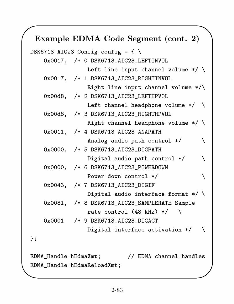
Example EDMA Code Segment (cont. 2)
DSK6713_AIC23_Config config = { \
0x0017, /* 0 DSK6713_AIC23_LEFTINVOL
Left line input channel volume */ \
0x0017, /* 1 DSK6713_AIC23_RIGHTINVOL
Right line input channel volume */\
0x00d8, /* 2 DSK6713_AIC23_LEFTHPVOL
Left channel headphone volume */ \
0x00d8, /* 3 DSK6713_AIC23_RIGHTHPVOL
Right channel headphone volume */ \
0x0011, /* 4 DSK6713_AIC23_ANAPATH
Analog audio path control */ \
0x0000, /* 5 DSK6713_AIC23_DIGPATH
Digital audio path control */ \
0x0000, /* 6 DSK6713_AIC23_POWERDOWN
Power down control */ \
0x0043, /* 7 DSK6713_AIC23_DIGIF
Digital audio interface format */ \
0x0081, /* 8 DSK6713_AIC23_SAMPLERATE Sample
rate control (48 kHz) */ \
0x0001 /* 9 DSK6713_AIC23_DIGACT
Digital interface activation */ \
};
EDMA_Handle hEdmaXmt; // EDMA channel handles
EDMA_Handle hEdmaReloadXmt;
2-83

✬
✫
✩
✪
Example EDMA Code Segment (cont. 3)
Int16 gXmtChan; // TCC code (see initEDMA())
/* Transmit side EDMA configuration */
EDMA_Config gEdmaConfigXmt = {
EDMA_FMKS(OPT, PRI, HIGH) | // Priority
EDMA_FMKS(OPT, ESIZE, 32BIT) | // Element size
EDMA_FMKS(OPT, 2DS, NO) | // 1 dimensional source
EDMA_FMKS(OPT, SUM, INC) | // Src update mode
EDMA_FMKS(OPT, 2DD, NO) | // 1 dimensional dest
EDMA_FMKS(OPT, DUM, NONE)| // Dest update mode
EDMA_FMKS(OPT, TCINT, NO)| // No EDMA interrupt
EDMA_FMKS(OPT, TCC, OF(0))| // Trans. compl. code
EDMA_FMKS(OPT, LINK, YES)| // Enable linking
EDMA_FMKS(OPT, FS, NO), // Use frame sync?
(Uint32) table, // Src address
EDMA_FMK (CNT, FRMCNT, NULL) | // Frame count
EDMA_FMK (CNT, ELECNT, SZ_TABLE),// Element cnt
EDMA_FMKS(DST, DST, OF(0)), //Dest address
EDMA_FMKS(IDX, FRMIDX, DEFAULT) | // Frame index
EDMA_FMKS(IDX, ELEIDX, DEFAULT), // Element index
2-84

✬
✫
✩
✪
Example EDMA Code Segment (cont. 4)
EDMA_FMK (RLD, ELERLD, NULL) | // Reload element
EDMA_FMK (RLD, LINK, NULL) // Reload link
};
/* Function Prototypes */
void initEdma(void);
void create_table(void);
void main(void){
DSK6713_AIC23_CodecHandle hCodec;
intr_reset(); /* Initialize interrupt system */
/* dsk6713_init() must be called before other
BSL functions */
DSK6713_init(); /* In the BSL library */
/* Start the codec. McBSP1 uses 32-bit words,
1 phase, 1 word frame */
hCodec = DSK6713_AIC23_openCodec(0, &config);
/* Change the sampling rate to 16 kHz */
DSK6713_AIC23_setFreq(hCodec,
DSK6713_AIC23_FREQ_16KHZ);
create_table(); /* You must write this function. */
2-85

✬
✫
✩
✪
Example EDMA Code Segment (cont. 4)
initEdma(); /* Initialize the EDMA controller
(See below) */
while(1); /* infinite loop */
} /* end of main() */
/**************************************************/
/* Create a table where upper 16-bits are samples */
/* of a sine wave with frequency f_left, and the */
/* lower 16 bits are samples of a sine wave with */
/* frequency f_right. */
/**************************************************/
void create_table(void){
Put your code to generate the sine table here.
}
/*************************************************/
/* initEdma() - Initialize the DMA controller. */
/* Use linked transfers to automatically restart */
/* at beginning of sine table. */
/*************************************************/
void initEdma(void)
{
/* Configure transmit channel */
2-86

✬
✫
✩
✪
Example EDMA Code Segment (cont. 5)
/* get hEdmaXmt handle, Set channel event to XEVT1 */
hEdmaXmt =EDMA_open(EDMA_CHA_XEVT1, EDMA_OPEN_RESET);
// get handle for reload table
hEdmaReloadXmt = EDMA_allocTable(-1);
// Get the address of DXR for McBSP1
gEdmaConfigXmt.dst = MCBSP_getXmtAddr(
DSK6713_AIC23_DATAHANDLE);
// then configure the Xmt table
EDMA_config(hEdmaXmt, &gEdmaConfigXmt);
// Configure the Xmt reload table
EDMA_config(hEdmaReloadXmt, &gEdmaConfigXmt);
// link back to table start
EDMA_link(hEdmaXmt,hEdmaReloadXmt);
EDMA_link(hEdmaReloadXmt, hEdmaReloadXmt);
// enable EDMA channel
EDMA_enableChannel(hEdmaXmt);
/* Do a dummy write to generate the first
McBSP transmit event */
MCBSP_write(DSK6713_AIC23_DATAHANDLE, 0);
}
2-87