AIXTRON Investor Presentation · AIXTRON Investor Presentation IR Presentation – Q1/2015 ......
37
AIXTRON Investor Presentation IR Presentation – Q1/2015 (FSE: AIXA, ISIN DE000A0WMPJ6, NASDAQ: AIXG, ISIN: US0096061041) © AIXTRON Investor Relations, April 2015
Transcript of AIXTRON Investor Presentation · AIXTRON Investor Presentation IR Presentation – Q1/2015 ......

AIXTRON Investor Presentation IR Presentation – Q1/2015 (FSE: AIXA, ISIN DE000A0WMPJ6, NASDAQ: AIXG, ISIN: US0096061041)
© AIXTRON Investor Relations, April 2015

Forward-Looking Statements
This document may contain forward-looking statements regarding the business, results of operations, financial condition and earnings outlook of AIXTRON within the meaning of the safe harbor provisions of the US Private Securities Litigation Reform Act of 1995. These statements may be identified by words such as “may”, “will”, “expect”, “anticipate”, “contemplate”, “intend”, “plan”, “believe”, “continue” and “estimate” and variations of such words or similar expressions. These forward-looking statements are based on our current views and assumptions and are subject to risks and uncertainties. You should not place undue reliance on these forward-looking statements. Actual results and trends may differ materially from those reflected in our forward-looking statements. This could result from a variety of factors, such as actual customer orders received by AIXTRON, the level of demand for deposition technology in the market, the timing of final acceptance of products by customers, the condition of financial markets and access to financing for AIXTRON, general conditions in the market for deposition plants and macroeconomic conditions, cancellations, rescheduling or delays in product shipments, production capacity constraints, extended sales and qualification cycles, difficulties in the production process, the general development in the semi-conductor industry, increased competition, fluctuations in exchange rates, availability of public funding, fluctuations and/or changes in interest rates, delays in developing and marketing new products, a deterioration of the general economic situation and any other factors discussed in any reports or other announcements field by AIXTRON with the U.S. Securities and Exchange Commission. Any forward-looking statements contained in this document are based on current expectations and projections of the Executive Board and on information currently available to it and are made as at the date hereof. AIXTRON undertakes no obligation to revise or update any forward-looking statements as a result of new information, future events or otherwise, unless expressly required to do so by law.
AIXTRON INVESTOR PRESENTATION
2

Who we are
Headquarters based in Herzogenrath, Germany
Worldwide presence with 12 sales/representatives offices
and production facilities
Company founded in 1983 – over 30 years of experience
760+ employees
Technology leader in deposition systems
More than 3,000 deposition systems delivered
all over the world
State of the art R&D center and demo facilities
Annual R&D budget of approx. € 60 Million
3 About aixtron
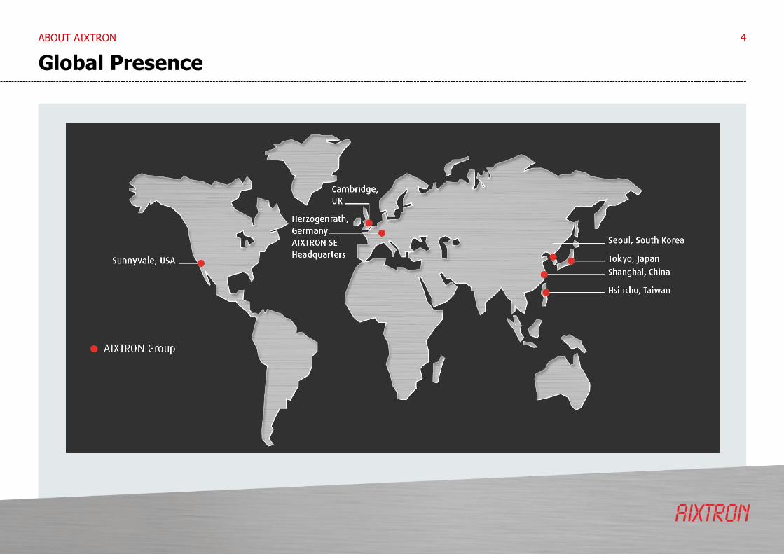
Global Presence
ABOUT AIXTRON 4

Our Vision
Technology. Materials. Performance.
Technology. We are the recognized technology leader in complex material deposition.
Materials.
We enable our customers to successfully shape the markets of the future, exploiting the potential offered by new materials.
Performance.
We deliver the performance driving economic success through our expertise, our employees and the quality of our products.
ABOUT AIXTRON 5
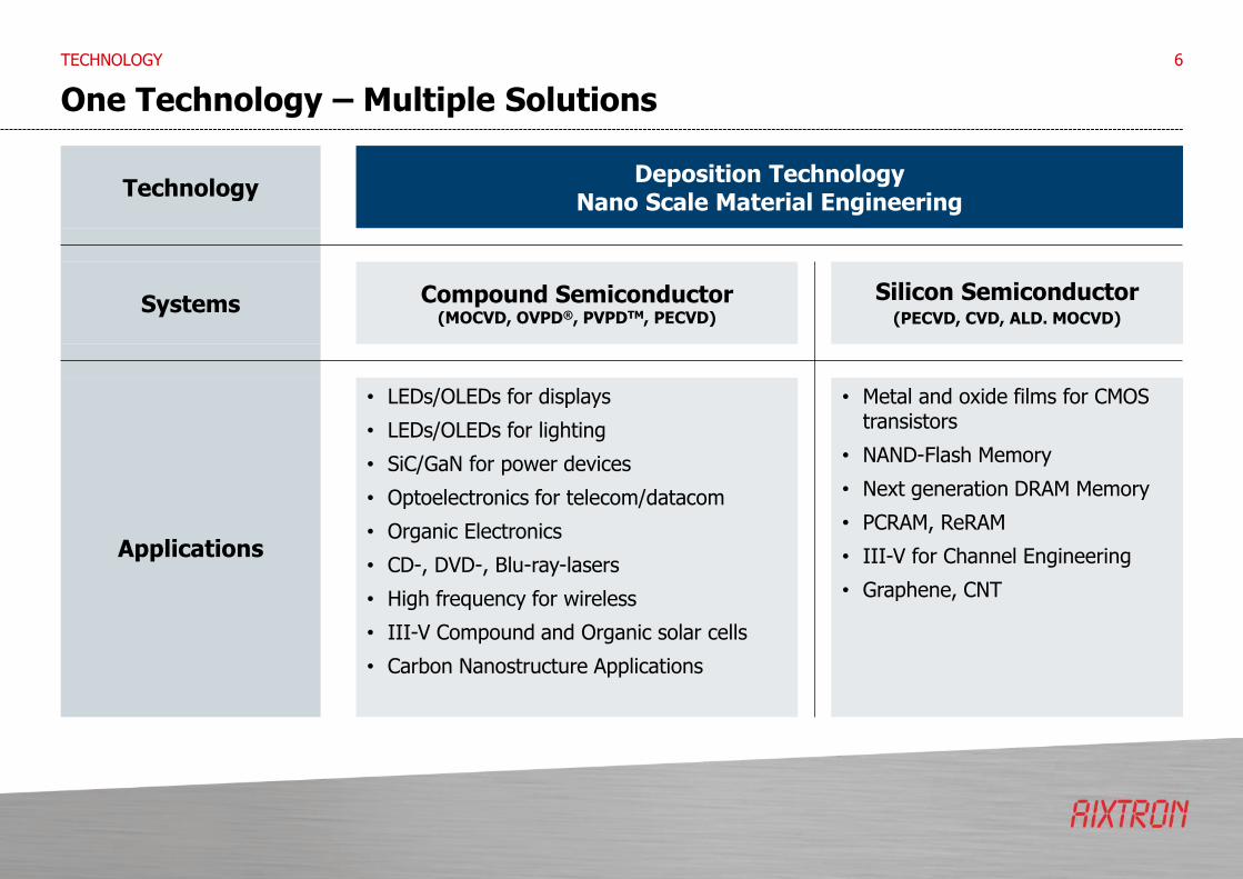
One Technology – Multiple Solutions
TECHNOLOGY
6
Technology Deposition Technology
Nano Scale Material Engineering
Systems Compound Semiconductor (MOCVD, OVPD®, PVPDTM, PECVD)
Silicon Semiconductor (PECVD, CVD, ALD. MOCVD)
Applications
• LEDs/OLEDs for displays
• LEDs/OLEDs for lighting
• SiC/GaN for power devices
• Optoelectronics for telecom/datacom
• Organic Electronics
• CD-, DVD-, Blu-ray-lasers
• High frequency for wireless
• III-V Compound and Organic solar cells
• Carbon Nanostructure Applications
• Metal and oxide films for CMOS transistors
• NAND-Flash Memory
• Next generation DRAM Memory
• PCRAM, ReRAM
• III-V for Channel Engineering
• Graphene, CNT

Compound Semiconductors – New AIX R6
• Close Coupled Showerhead® (CCS)
• CoO benefit vs. prior generation systems: > 30%
• Capacity increase vs. largest prior generation system: > 60%
• Throughput benefit vs. prior generation systems: >120%
AIX R6 Setting New Standards in LED Manufacturing
AIXTRON TECHNOLOGIES AND PRODUCTS 7
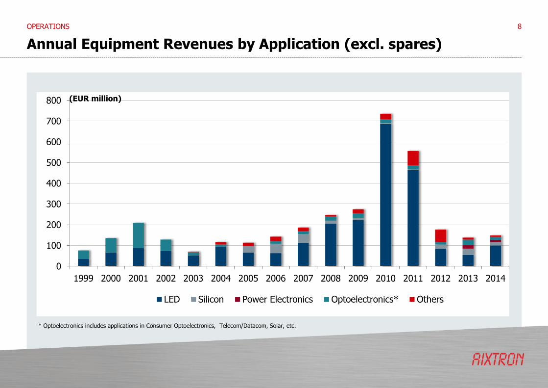
Annual Equipment Revenues by Application (excl. spares)
OPERATIONS 8
0
100
200
300
400
500
600
700
800
1999 2000 2001 2002 2003 2004 2005 2006 2007 2008 2009 2010 2011 2012 2013 2014
LED Silicon Power Electronics Optoelectronics* Others
(EUR million)
* Optoelectronics includes applications in Consumer Optoelectronics, Telecom/Datacom, Solar, etc.

Order Intake per Quarter
OPERATIONS 9
Source: Deutsche Bank Equity Research, AIXTRON SE
0
50
100
150
200
250
1Q98
2Q98
3Q98
4Q98
1Q99
2Q99
3Q99
4Q99
1Q00
2Q00
3Q00
4Q00
1Q01
2Q01
3Q01
4Q01
1Q02
2Q02
3Q02
4Q02
1Q03
2Q03
3Q03
4Q03
1Q04
2Q04
3Q04
4Q04
1Q05
2Q05
3Q05
4Q05
1Q06
2Q06
3Q06
4Q06
1Q07
2Q07
3Q07
4Q07
1Q08
2Q08
3Q08
4Q08
1Q09
2Q09
3Q09
4Q09
1Q10
2Q10
3Q10
4Q10
1Q11
2Q11
3Q11
4Q11
1Q12
2Q12
3Q12
4Q12
1Q13
2Q13
3Q13
4Q13
1Q14
2Q14
3Q14
4Q14
*1Q
15
Compound Semiconductor Market China Investments
driven by notebook
backlighting
driven by LED TV
driven by strategic China investments
(EUR million)
driven by mobile phone
penetration
driven by telecom/datacom and mobile phone
* total order intake including spares & service from Q1/15

5-Point-Program - Return to Sustainable Profitability
OPERATIONS 10
Customer
Technology & Products
Finance
Efficiency
Employees
1
2
3
4
5
Focusing on customer benefit
Putting unique technology portfolio to more effective use, further strengthening future products
Optimizing process and project structures systematically
Value driven financial orientation
Strengthening AIXTRON’s culture, instill self-responsibility, fortifying communication
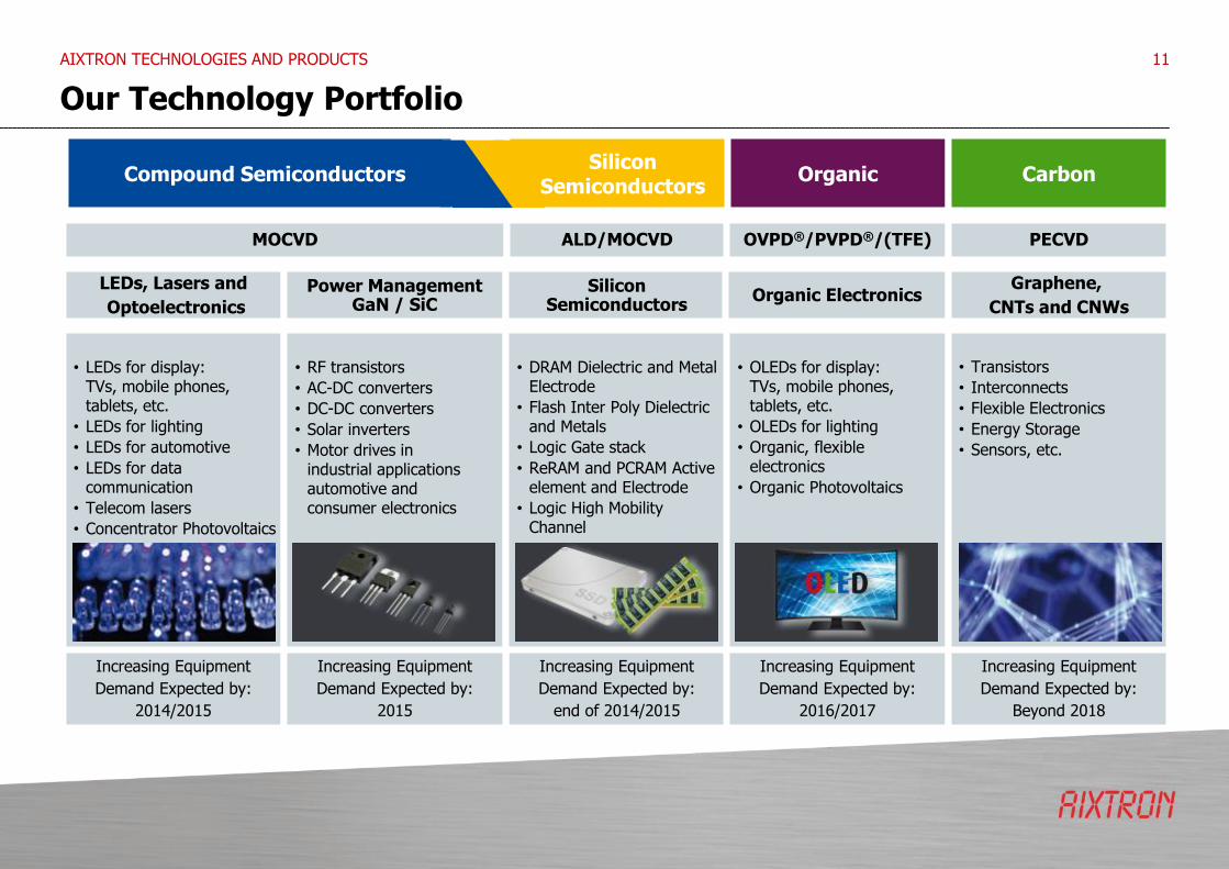
Compound Semiconductors
MOCVD ALD/MOCVD
LEDs, Lasers and
Optoelectronics
• LEDs for display: TVs, mobile phones, tablets, etc.
• LEDs for lighting
• LEDs for automotive
• LEDs for data communication
• Telecom lasers
• Concentrator Photovoltaics
Increasing Equipment
Demand Expected by:
2014/2015
Our Technology Portfolio
11
Silicon Semiconductors
• RF transistors
• AC-DC converters
• DC-DC converters
• Solar inverters
• Motor drives in industrial applications automotive and consumer electronics
Power Management GaN / SiC
• DRAM Dielectric and Metal Electrode
• Flash Inter Poly Dielectric and Metals
• Logic Gate stack
• ReRAM and PCRAM Active element and Electrode
• Logic High Mobility Channel
Silicon Semiconductors
Increasing Equipment
Demand Expected by:
end of 2014/2015
Increasing Equipment
Demand Expected by:
2015
• OLEDs for display: TVs, mobile phones, tablets, etc.
• OLEDs for lighting
• Organic, flexible electronics
• Organic Photovoltaics
• Transistors
• Interconnects
• Flexible Electronics
• Energy Storage
• Sensors, etc.
Organic Electronics Graphene,
CNTs and CNWs
Organic Carbon
OVPD®/PVPD®/(TFE) PECVD
Increasing Equipment
Demand Expected by:
2016/2017
Increasing Equipment
Demand Expected by:
Beyond 2018
AIXTRON TECHNOLOGIES AND PRODUCTS

71.6 72.859.6 64.2 66.4 70.7 65.2
79.0
24 - Month Business Development
Financials 12
Q2/2013 Q3/2013 Q4/2013 Q1/2014 Q2/2014 Q3/2014 Q4/2014 Q1/2015
45.3 46.2 51.1 43.9 46.2 45.6 58.0
40.3
41.4 47.0 49.0 49.5 49.7 50.2 49.3 48.9Order Intake1
(€ million)
Total Revenues
Order Backlog
1) total order intake including spares & service from Q1/2015; adopted for Q2/2013~Q4/2014 for comparison reasons
USD order intake and backlog were recorded at the prevailing budget rate (2015: $1.25/€)
USD revenues were converted at the actual period average FX rate (Q1/2015: $1.156/€)
*
@ $1.30
@ $1.30
@ 1.327
@ $1.35
@ $1.35
@ $1.334
*) revalued on Jan.1, 2015 to €69.0m at $1.25/€
@ $1.25
@ $1.25
@ $1.16

Revenue Analysis
OPERATIONS 13
Q1/2015: by region
Q1/2015: by equipment & spares
72%
28%
Spares
Equipment
Q1/2015: by end application
(equipment only)
49%
34%
9%4%
4%
82%
13%
5%
USA
Europe
Asia
Power Electronics
Silicon
LED
Optoelectronics
Others

Consolidated Income Statement*
14
(€ million) Q1/15 Q1/14
Restated +/- Q1/15
Q4/14 Restated
+/-
Revenues 40.3 43.9 -8% 40.3 58.0 -31%
Cost of sales 31.5 34.01 -7% 31.5 47.61 -34%
Gross profit 8.8 10.01 -12% 8.8 10.41 -15%
Gross Margin 22% 23%1 -1 pp 22% 18%1 4 pp
Selling expenses 3.3 3.11 6% 3.3 4.01 -18%
General & admin expenses 4.3 5.1 -16% 4.3 5.4 -21%
R&D 12.9 13.7 -6% 12.9 21.2 -39%
Net other op.(income)/expenses -3.0 -1.1 -173% -3.0 -1.3 -126%
EBITDA -6.4 -7.1 10% -6.4 -13.9 54%
EBIT -8.8 -10.9 19% -8.8 -18.9 53%
EBIT Margin -22% -25% 3 pp -22% -33% 11 pp
Result before tax -8.5 -10.7 20% -8.5 -18.7 54%
Pre-Tax Margin -21% -24% 3 pp -21% -32% 11 pp
Net result -9.5 -11.8 19% -9.5 -19.1 50%
Net Return on Sales -23% -27% 4 pp -23% -33% 10 pp
Financials
*) rounded figures; may not add up 1) Restated; please refer to “Accounting Policies” in Q1-Report

Consolidated Statement of Financial Position*
15
(€ million) 31/3/15 31/12/14 31/3/14
Property, plant & equipment 79.4 77.3 80.2
Goodwill 65.7 64.8 64.2
Other intangible assets 2.3 2.5 2.8
Others 5.0 4.6 5.6
Non-current assets 152.5 149.2 152.8
Inventories, WIP & Finished Goods 88.8 81.7 67.0
Trade receivables 26.2 26.3 26.2
Others 12.3 8.3 15.0
Cash & Cash Equivalents incl. CD 263.2 268.1 292.0
Current Assets 390.5 384.4 400.3
Shareholders' equity 419.2 415.7 453.1
Non-current liabilities 1.3 1.3 2.2
Trade payables 12.8 16.4 17.1
Advance payments from customers 79.6 66.9 49.8
Others 30.1 33.2 31.0
Current liabilities 122.4 116.5 97.8
Balance Sheet total 543.0 533.5 553.2
Financials
*) rounded figures; may not add up

Consolidated Statement of Cash Flows*
16
(€ million) Q1/15 Q1/14 Q1/15 Q4/14
Cash Flow from operating activities -10.1 -9.8 -10.1 9.8
Cash Flow from investing activities 11.3 -24.3 11.3 -29.3
Cash Flow from financing activities 0.0 0.1 0.0 0.3
Exchange rate changes 6.2 -0.4 6.2 0.7
Net change in Cash & Cash Equivalents 7.4 -34.5 7.4 -18.4
Cash & Cash Equivalents (beginning of period) 116.6 167.5 116.6 135.0
Cash & Cash Equivalents (end of period) 124.0 133.0 124.0 116.6
Change in Cash deposits -14.8 20.3 -14.8 25.4
Free Cash Flow1 -12.12 -13.8 -12.12 5.9
Capex 3.5 4.0 3.5 4.0
Financials
*) rounded figures; may not add up 1) Operating CF + Investing CF + Changes in Cash Deposits 2) Excl. an effect of €-1.5m resulting from a short term loan prior to the acquisition of PlasmaSi Inc.

Market Prospects
Short-Term • Further increasing adoption of LEDs for exterior, public infrastructure & commercial lighting
• Increased adoption of LEDs for consumer & residential lighting
• Market positioning of the new AIX R6 MOCVD tool for LED manufacturing
• Increasing adoption of GaN for power electronics
• Increased emergence of silicon carbide (SiC) hybrid automotive & photovoltaic applications
• Next generation NAND, DRAM & PRAM memory applications
Mid- to Long-Term • Development of organic semiconductors applications using efficient deposition and thin-film
encapsulation technologies
• Development of GaN-on-Si based power electronics or LEDs
• Further development of plastic electronics/flexible TFT backplanes
• Increased development for specialized compound solar cells
• Higher demand for High-k as well as interconnect components
• Progress in the convergence of compound material applications, e. g. substituting materials in the silicon semiconductor industry
• Development of applications using carbon nanostructures including graphene
FUTURE MARKETS 17

AIXTRON INVESTOR PRESENTATION 18

LED Lighting Market: Multiple Tipping Points
INDUSTRY & MARKETS 19
Various Applications
Different Regions
Numerous Players
LED Lighting Cycle
Source: : AIXTRON, McKinsey 2012

0
10,000
20,000
30,000
40,000
50,000
60,000
2014e
2015e
2016e
2017e
2018e
HB L
ED
Mark
et (2
" Equiv
ale
nt W
afe
r in
000)
Mobile & Others Display Lighting
Increasing LED Area Demand Driving Growth
INDUSTRY & MARKETS 20
0
50
100
150
2014e
2015e
2016e
2017e
2018e
HB L
ED
Mark
et (b
n u
nits)
Mobile & Others Display Lighting
• Growth through increasing LED-unit and area demand
• Consistent epitaxial area growth will trigger equipment demand
• LED-lighting gaining further momentum
Based on compilation of latest opinions by: DisplaySearch; Strategies Unlimited; Displaybank; Gartner Dataquest; IMS Research.; McKinsey Lighting Report
(0.1mm²) (0.25mm²) (0.75-1mm²)
LED Units 2” Equivalent Wafer
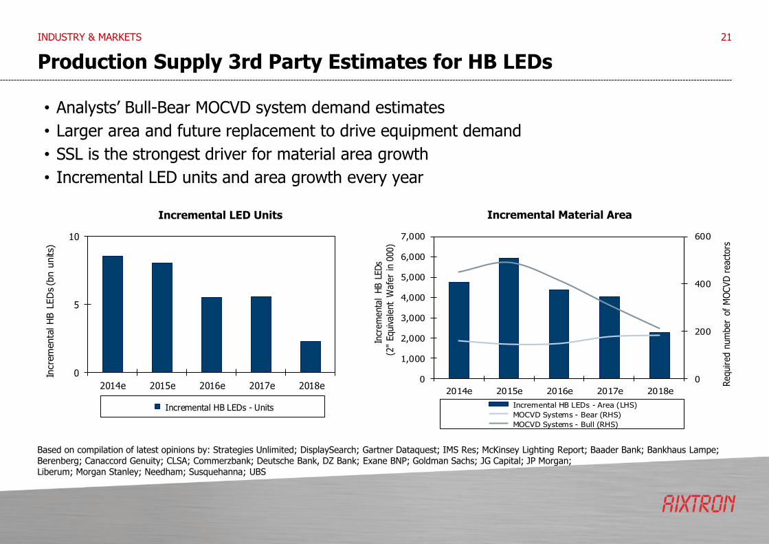
Production Supply 3rd Party Estimates for HB LEDs
INDUSTRY & MARKETS 21
• Analysts’ Bull-Bear MOCVD system demand estimates
• Larger area and future replacement to drive equipment demand
• SSL is the strongest driver for material area growth
• Incremental LED units and area growth every year
Based on compilation of latest opinions by: Strategies Unlimited; DisplaySearch; Gartner Dataquest; IMS Res; McKinsey Lighting Report; Baader Bank; Bankhaus Lampe; Berenberg; Canaccord Genuity; CLSA; Commerzbank; Deutsche Bank, DZ Bank; Exane BNP; Goldman Sachs; JG Capital; JP Morgan; Liberum; Morgan Stanley; Needham; Susquehanna; UBS
Incremental LED Units Incremental Material Area
0
5
10
2014e 2015e 2016e 2017e 2018e
Incre
menta
l H
B L
ED
s (b
n u
nits)
Incremental HB LEDs - Units
0
200
400
600
0
1,000
2,000
3,000
4,000
5,000
6,000
7,000
2014e 2015e 2016e 2017e 2018e
Required n
um
ber
of
MO
CVD r
eact
ors
Incr
em
enta
l HB L
EDs
(2"
Equiv
ale
nt
Wafe
r in
000)
Incremental HB LEDs - Area (LHS)
MOCVD Systems - Bear (RHS)
MOCVD Systems - Bull (RHS)

0%
5%
10%
15%
20%
25%
30%
35%
40%
0.0
0.5
1.0
1.5
2.0
2.5
3.0
3.5
4.0
4.5
201
3
201
4
201
5e
201
6e
201
7e
201
8e
201
9e
202
0e
202
1e
202
2e
LED lamps (LHS)
LED lamps as % of total
LED Lighting Market Estimates
INDUSTRY & MARKETS 22
Source: IHS Q1/2015
Globalization and urbanization to drive LED lighting opportunities:
• Emerging countries: need for energy efficient lighting solutions
• Developed countries: SSL driven by expanding renovation market
• Outdoor: Early adoption streetlight replacement market
• Commercial: LED Light Bulb reaching price tipping point
LED Market Forecast Global LED lamp shipments
bill
ion u
nits
LED
penetr
ation
-
2
4
6
8
10
12
14
16
2014 2015e 2016e 2017e 2018e 2019e
Others Automotive Signs Lighting Mobile/Display
Mark
et
size
(in
US$ b
illio
n)

A-19 Bulb: 60W* LED Replacement – Global Pricing
INDUSTRY & MARKETS 23
Source: Various websites; AIXTRON
* According to Tab. 6 of EU-Regulation 244/2009 requiring >700lm minimum for 60W
Global Brands: Samsung, Osram, Philips, GE, Toshiba, etc.
New light bulbs with higher lm/W being offered
Brand suppliers increasingly offering attractively priced devices
Regions Halogen CFL LED QoQ +/-
Low High LED vs. Hal.
(x) LED vs. CFL
(x)
Average US $ 1.5 $ 1.7 $ 7 10% $6 $9 4.9x 4.5x
Average Japan $ 1.6 $ 3.2 $ 12 1% $7 $15 7.3x 3.7x
Average EU $ 1.4 $ 4.2 $ 9 10% $7 $14 6.6x 2.2x
Average Korea $ 1.5 $ 3.3 $ 10 1% $7 $13 6.3x 2.9x
Average Taiwan $ 2.5 $ 3.9 $ 9 3% $6 $10 3.5x 2.2x
Average $ 1.7 $ 3.3 $ 9 5% $6 $15 5.5x 2.9x

Compound Semiconductors – System Generations
• Extendibility: Extensive choice of configurations and enhancements
• Scalability: Multiple technologies on one platform
• Productivity: Highest throughput, best yield, fastest growth rates
Two Reactor Technologies Planetary Reactor® & Close Coupled Showerhead® (CCS)
AIXTRON TECHNOLOGIES AND PRODUCTS
24
Year of Introduction Technology Chambers
2002 • G3 Planetary
• 19x2” CCS
• 24x2”, 8x4”
• 19x2”
2006 • G4 HT Planetary
• CRIUS® CCS
• 42x2”, 11x4”, 6x6”
• 31x2”, 12x3”, 7x4”, 3x6”, 1x12”
2010/ 2011 • G5 HT Planetary
• CRIUS® II-eXL CCS
• 56x2”, 14x4”, 8x6’’, 5x8’’
• 75x2”, 19x4”
2012 • G5+ HT Planetary • 5x8” GaN-on-Si Technology
2014 • G5 WW
• AIX R6
• 12x4”, 8x6”
• 121x2”, 31x4”, 12x6”

Compound Semiconductors – MOCVD
• Addressing multiple industries
• Established industry standard & market leading
• Configurable, extendable common platform
• Introduced the latest MOCVD technology - AIX R6
Two Reactor Technologies Planetary Reactor® & Close Coupled Showerhead® (CCS)
AIXTRON TECHNOLOGIES AND PRODUCTS 25
Planetary Reactor®
AIX G5+, 5x8 Close Coupled Showerhead®
AIX R6, 31x4”
• Unique Planetary reactor design
• Horizontal reactor type
• Patented CCS Technology
• Vertical reactor design
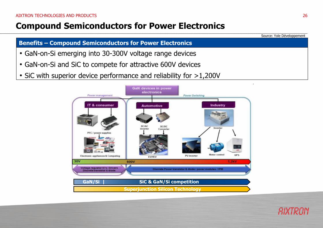
Compound Semiconductors for Power Electronics
AIXTRON TECHNOLOGIES AND PRODUCTS 26
Source: Yole Développement
GaN/Si | SiC & GaN/Si competition
Superjunction Silicon Technology
Benefits – Compound Semiconductors for Power Electronics
• GaN-on-Si emerging into 30-300V voltage range devices
• GaN-on-Si and SiC to compete for attractive 600V devices
• SiC with superior device performance and reliability for >1,200V

Compound and Silicon Semiconductors – Two Converging Worlds
AIXTRON TECHNOLOGIES AND PRODUCTS 27
Compound Semiconductors
• Dominated by Small Wafers – 2”, 4” & 6”
• Low Level of Automation and Fab Integration
• Complex Binning Process Required
• No Industry Wide Roadmap
• AIXTRON G5+ MOCVD Planetary Reactor Offers Flexibility; Accommodating Wafer Sizes From 2” to 200 mm
• Process Migration Path Without Changing Platforms
• 300 mm Wafers (450 mm on Roadmap)
• Fully Automated Fabs
• Excellent Yield Management Practices
• Recognized Industry Roadmap

Silicon Semiconductors - ALD
28
Product Description – ALD
• Up to 3 patented TriJet vaporizers
• Small volume confined process space ensure short ALD cycle time
• > 40 % less precursor consumption • Efficient purge
• Isolated multi wafer processing with
> 40% higher throughput
• Close Coupled Showerhead for uniform distribution
• Flexibility and ease of maintenance
• 300mm ALD Technology
• QXP-8300 Mini-batch system
• High throughput : 2 Process Chambers – 8 stations
• Up to 3 vaporizers and one bubbler
• Applications : DRAM, Logic and Flash High k Dielectric Metal electrode : ReRAM and PCRAM Active elements
• Proven in HVM with >40% lower CoO and >90% Uptime in DRAM and Flash Fabs
“Best-in class technology, state of the art deposition system, lowest CoO”
AIXTRON TECHNOLOGIES AND PRODUCTS
Product Features

Silicon Semiconductors – ALD and MOCVD
29
Benefits – ALD and MOCVD
• Multi generation film development for Memory and Logic
• Advanced technology nodes require high productivity ALD equipment
• Introduction of new materials drives ALD and MOCVD processes
AIXTRON TECHNOLOGIES AND PRODUCTS
-
100
200
300
400
500
600
Worldwide Fab Capacity
all nodes
Worldwide Fab Capacity
≤ 22nm
2014 2019e
ReRAM
III-Vs /Si
nanometers
22 Transistor gate length
10
CNT Graphene
14 7
Silicon ICs: “Decade of Materials”
R&D HVM
AIXTRON Positioning
Source: Gartner 2015
(2014: Indexed=100) CAGR: 38%
CAGR: 2%
Rapid growth in advanced tech nodes
5
Metal Gates
High-k dielectrics
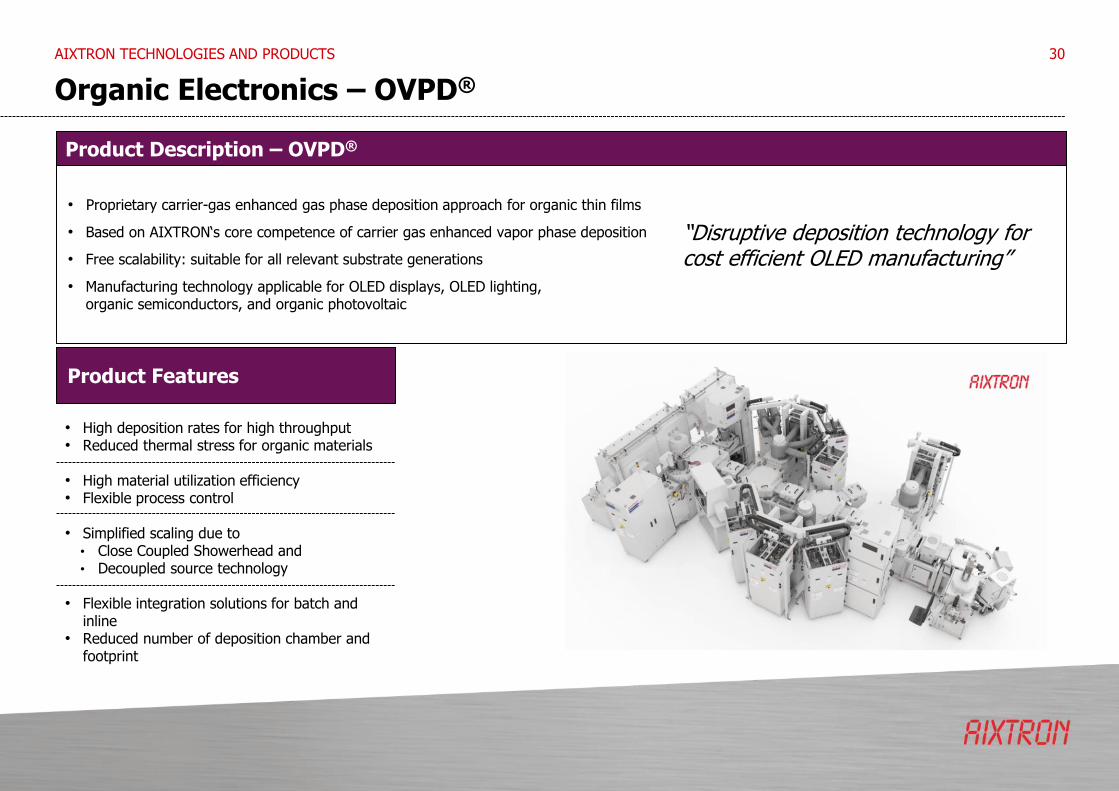
Organic Electronics – OVPD®
30
• Proprietary carrier-gas enhanced gas phase deposition approach for organic thin films
• Based on AIXTRON‘s core competence of carrier gas enhanced vapor phase deposition
• Free scalability: suitable for all relevant substrate generations
• Manufacturing technology applicable for OLED displays, OLED lighting, organic semiconductors, and organic photovoltaic
• High deposition rates for high throughput • Reduced thermal stress for organic materials
• High material utilization efficiency • Flexible process control
• Simplified scaling due to
• Close Coupled Showerhead and • Decoupled source technology
• Flexible integration solutions for batch and inline
• Reduced number of deposition chamber and footprint
Product Description – OVPD®
Product Features
“Disruptive deposition technology for cost efficient OLED manufacturing”
AIXTRON TECHNOLOGIES AND PRODUCTS
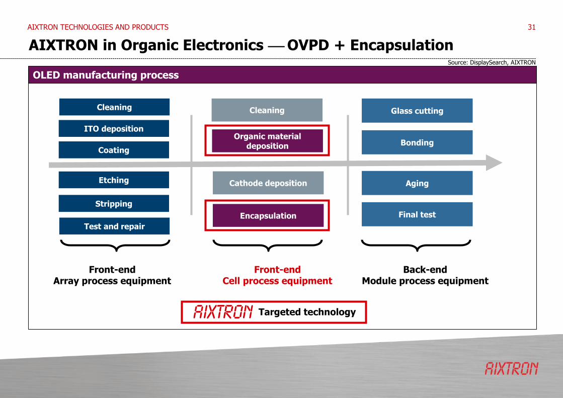
AIXTRON in Organic Electronics OVPD + Encapsulation
AIXTRON TECHNOLOGIES AND PRODUCTS 31
Source: DisplaySearch, AIXTRON
Front-end Array process equipment
Front-end Cell process equipment
Coating
Etching
Stripping
Test and repair
ITO deposition
Cleaning
Organic material deposition
Encapsulation
Cathode deposition
Cleaning Glass cutting
Bonding
Aging
Final test
Back-end Module process equipment
Targeted technology
OLED manufacturing process

Front-end Cell Process Equipment
MARKET OPPORTUNITIES 32
Cleaning Deposition Cathode
deposition Encapsulation Module
preparation Automation
5%
40%
10% 20%
5%
20%
Cumulative Capex
45%
55%
75%
80%
100%
Focus Activities
Key competency: Thin-film deposition
Value creation: 60%
Source: IHS; AIXTRON internal estimates

Carbon Nanostructures – PECVD
33
Product features
• Proprietary thermal and plasma enhanced chemical vapour deposition technology
• Excellent uniformity and reproducibility with fast turnaround cycle times
• BM platform: BM R&D (2-inch), BM Pro (4-inch and 6-inch), BM GB (4-inch glovebox), BM HT (high temperature, 1,700C), BM300T (300mm)
• Graphene and carbon nanotube films for electronics, energy storage, thermal management, sensors and flexible/transparent applications
Graphene and Carbon Nanotube Deposition Systems
• Fast response heater and turnaround
• Thermal CVD
• Substrate and top heating
• Closed loop infrared wafer temperature control
• Plasma enhanced CVD with frequency control
• Flexible processing for different applications
• Low cost of ownership
• Easy maintenance and cleaning
• User management features and growth library
Graphene (2D) and Carbon nanotube (1D)
Unique combination of high electrical/ thermal conductivity, mobility, flexibility and transparency
Serving R&D market today
AIXTRON BM Pro
Production ready for tomorrow
AIXTRON BM300T
Material Properties
AIXTRON Technology
Enabling Applications
AIXTRON TECHNOLOGIES AND PRODUCTS

Technology Position
AIXTRON TECHNOLOGIES AND PRODUCTS 34
R&D Demo &Qualification Pilot Production High Volume Production
MOCVD for III-V on Silicon
Carbon
Thin-Film Encapsulation for
OLED
OVPD for OLED deposition
ALD for Memory Customer B & C
ALD for Memory Customer A
MOCVD for LEDs, Lasers and
Optoelectronics
MOCVD for Power Management
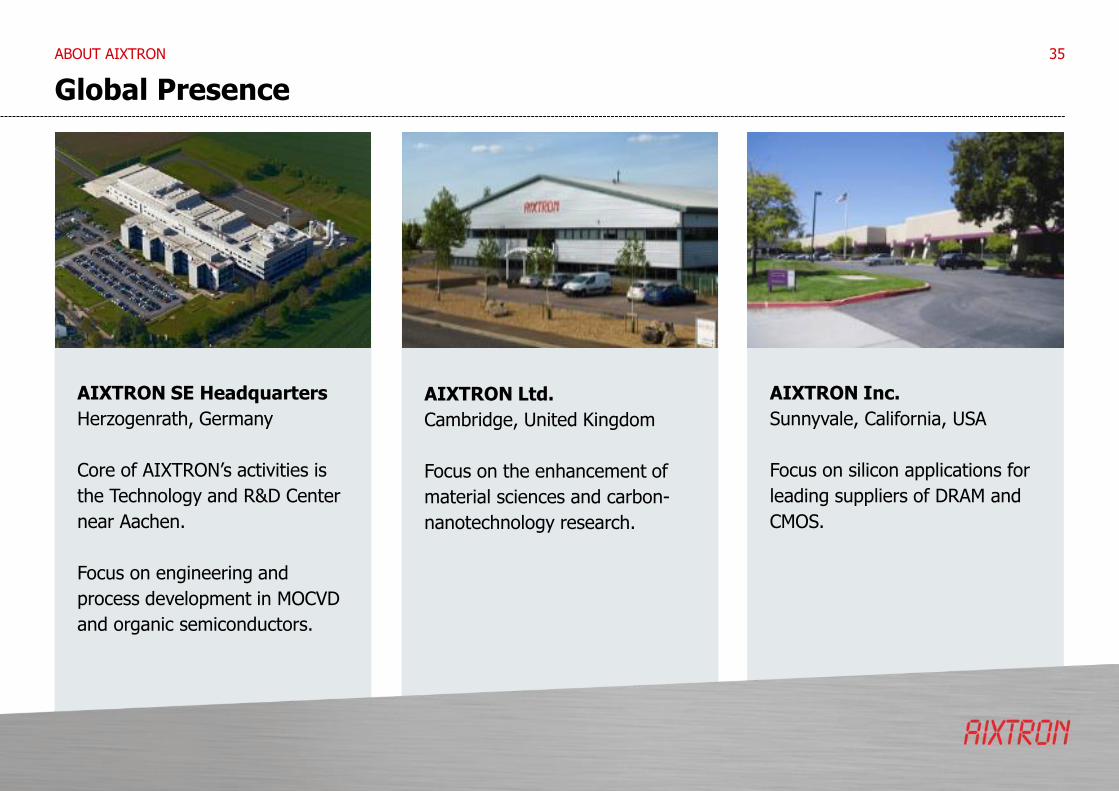
Global Presence
AIXTRON SE Headquarters
Herzogenrath, Germany
Core of AIXTRON’s activities is
the Technology and R&D Center
near Aachen.
Focus on engineering and
process development in MOCVD
and organic semiconductors.
AIXTRON Inc.
Sunnyvale, California, USA
Focus on silicon applications for
leading suppliers of DRAM and
CMOS.
AIXTRON Ltd.
Cambridge, United Kingdom
Focus on the enhancement of
material sciences and carbon-
nanotechnology research.
35 ABOUT AIXTRON

Financial Calendar & Contact Data
• May 20, 2015 Annual General Meeting, Aachen
• July 28, 2015 H1/2015 Results, Conference Call
• October 2015 9M/2015 Results, Conference Call
• February 2016 FY 2015 Results, Conference Call
For further information please contact:
Investor Relations & Corporate Communications AIXTRON SE Dornkaulstr. 2 52134 Herzogenrath, Germany
IR Team Europe Phone: +49 (241) 8909-444 Email: [email protected]
IR Team USA – Andrea Su Phone: +1 (408) 747-7140 ext. 1292 Email: [email protected]
36

AIXTRON SE Dornkaulstr. 2 52134 Herzogenrath Germany Phone +49 (2407) 9030-0 Fax +49 (2407) 9030-40 E-Mail [email protected]
Thank you very much for your attention.