AHK SMPS P4 TR Final
17
Submitted By: Alex Kremnitzer Date: 05-04-2011 Date Performed: 04-26-2011 Lab Partners: None Switch Mode Power Supply Technical Report 4 Milwaukee School of Engineering ET-3100 Electronic Circuit Design
-
Upload
alexander-kremnitzer -
Category
Documents
-
view
76 -
download
1
Transcript of AHK SMPS P4 TR Final
Submitted By: Alex Kremnitzer
Date: 05-04-2011
Date Performed: 04-26-2011
Lab Partners: None
Switch Mode Power SupplyTechnical Report 4
Milwaukee School of Engineering ET-3100 Electronic Circuit Design

1
Abstract
In this design, a positive DC Switch Mode Power Supply with short circuit hard current limiting was designed, evaluated and tested. The design was based on the SG3524 Regulating Pulse Width Modulator integrated circuit.
The tested circuit verified the validity of the design. The load voltage remained constant at 8.5VDC and was able to supply the required load current of 250mA. The circuit was able to supply the load current until the short circuit current was reached upon which it then went into hard current limiting mode.
Efficiency was an improvement based on prior linear power supply circuits, being 74.5%. Both line and load regulation was less than 1%. The design does have the limitation of being noisy and the ripple voltage on the load was greater than with previous linear designs.
Introduction
The design constraints of the power supply were to provide 8.5VDC for load current of 250mA. The output current is to be hard limited at 125% of the normal load current and the load ripple voltage is to be less than 50mVpp. The circuit was designed, simulated and constructed.
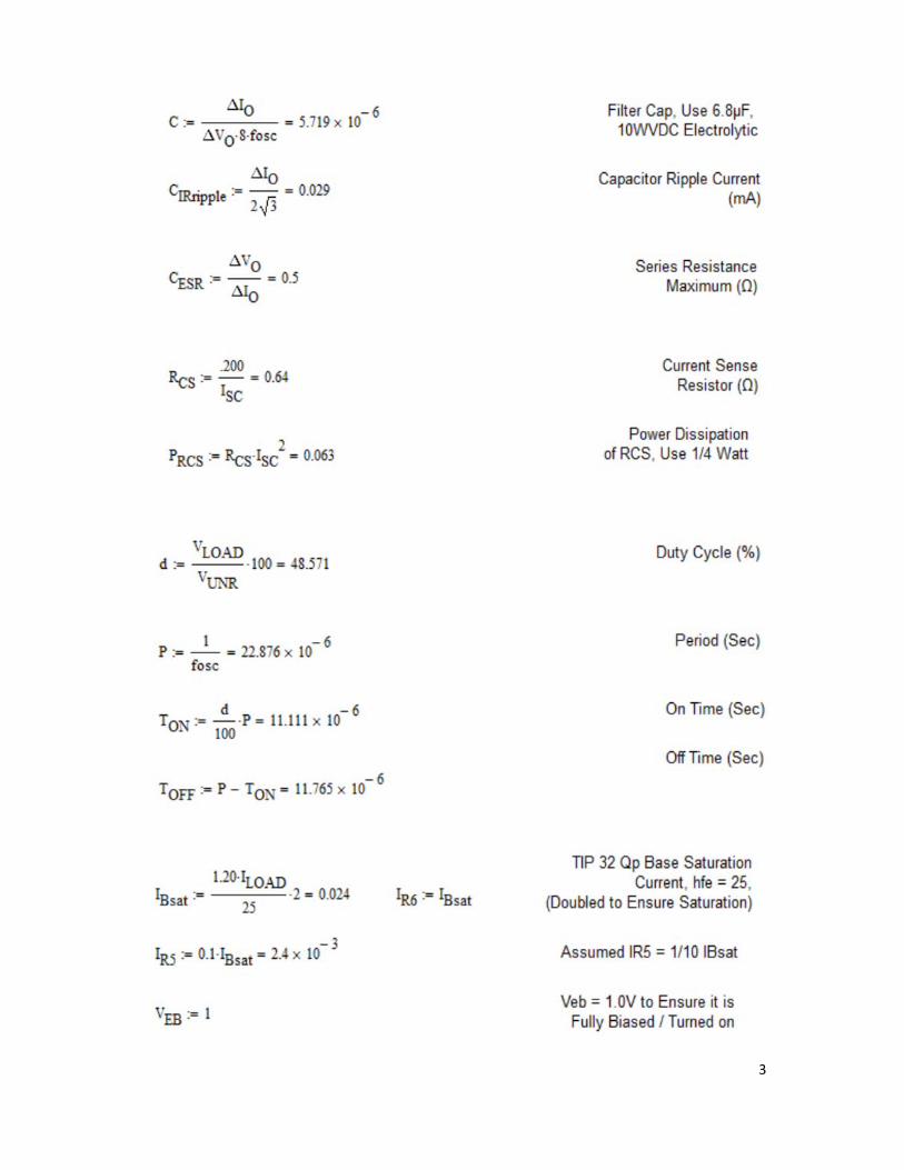
The circuit shown in the Appendix was constructed. Component measurements were taken using a Meterman Model LCR55 LCR Meter. In the lab, key measurements were taken using a Fluke Model 87III Multimeter and a Hewlett Packard 54602A Oscilloscope. The circuit was supplied from a Tenma Model UTC 72-5085 Power Supply. The following formulas were used in the design of the power supply circuit:

2
3

4
Calculations for Line Regulation:

5
Calculations for Load Regulation:
Calculations for Power Supply Impedance:
Calculations for Power Supply Efficiency:
PIN includes the power dissipated by all the components of the circuit while POUT is the power dissipated just in the load.

6
Calculations for Ripple Rejection Ratio:
Error Analysis Calculation Formulas:
Simulation Validation
Table 1: Calculated versus Simulated Results
Table 2: Simulated Line Regulation (mV/V)

7
Table 3: Simulated Load Regulation (mV/A)
Table 4: Simulated Power Supply Impedance (Ω)
Table 5: Simulated Ripple Rejection
Table 6: Simulated Power Supply Efficiency (%)

8
Analysis of Simulation Results
Overall the simulation verified the calculated values as shown in Table 1. The Load Voltage and Current were close to the calculated values. However the oscillator frequency was much lower than calculated. The values for the timing resistor (RT) and capacitor (CT) were verified to be correct. The duty cycle was also lower than calculated. Since the frequency timing component values and calculations were verified to be correct, I assumed the variances were from the circuit model of the SG3524 Regulating Pulse Width Modulator integrated circuit.
With the exclusion of the ripple rejection, the simulated circuit’s regulation and efficiency was good. See Tables 2 through 6. The simulated values for the Line Regulation were 4mV/V. Load Regulation was good at 0.16mV/V. Power Supply impedance simulations yielded a value of 0.16Ω. The simulated efficiency for rated load current of 250mA was 84% and at 50% of rated current was 78%. Ripple Rejection was simulated with an input ripple of 50mVpp and was poor yielding -32dB for a filter capacitor of 6.8uF and -12dB for 68uF.

Design
Validatio
n and Tes
Figur
Figu
Figur
sting
Figure 1: V
e 2: Voltage
ure 3: ΔVo w
re 3: ΔVo wi
Voltage befo
e at Base of
with 6.8uF F
ith 68uF Fil
re Inductor
f Pass Trans
Filter Capac
lter Capacit
r
sistor
citor
tor
9

10
RL=2Ω Table 7: Component Value Error Analysis
Table 8: Calculated versus Measured Values

11
Table 9: Line Regulation (mV/V)
Table 10: Load Regulation (mV/A)
Table 11: Power Supply Impedance (Ω)
Table 12: Ripple Rejection
Table 13: Power Supply Efficiency (%)
12
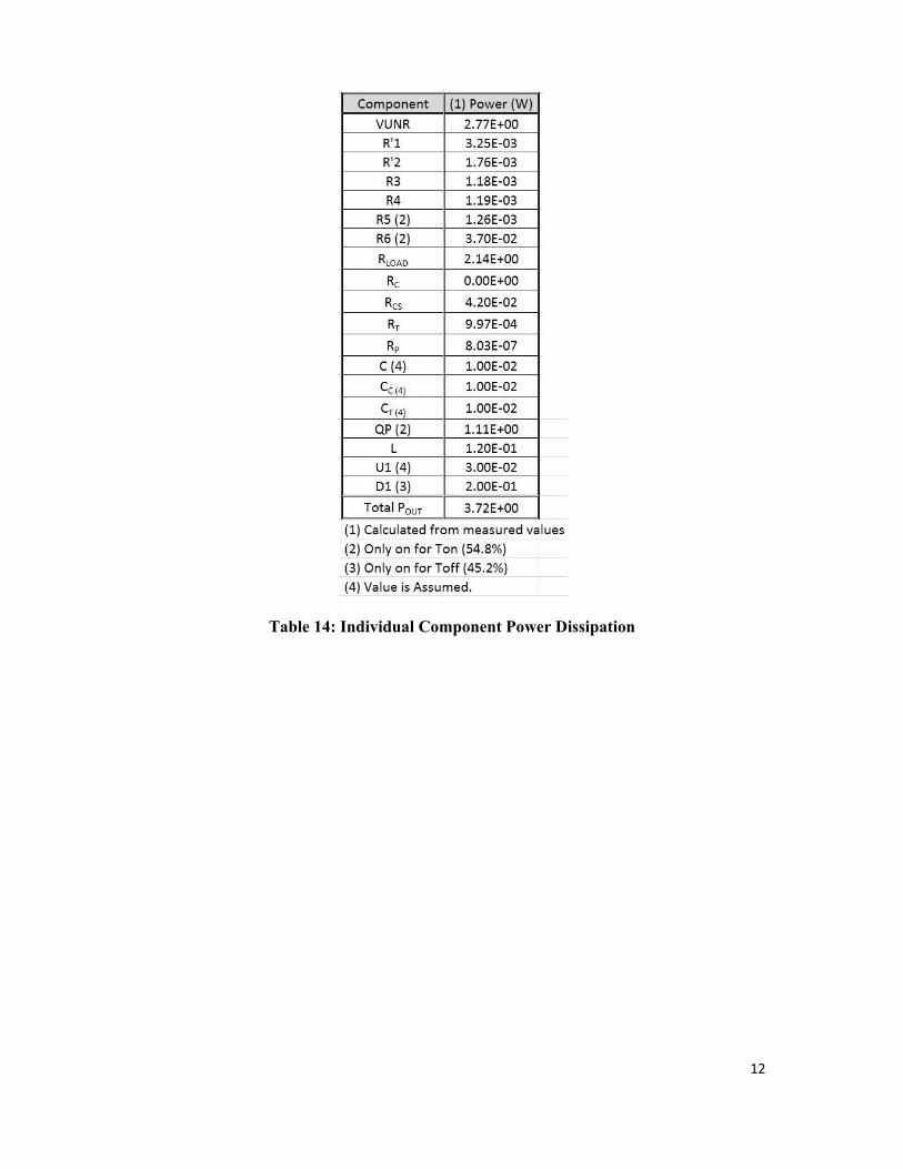
Table 14: Individual Component Power Dissipation

13
Analysis of Testing Results Component Values
The values of all components measured were within their tolerance ratings as shown in Table 7. The Current Sense Resistor, RCS was 0.64Ω to give a short circuit current limit of 125% of rated current (250mA). However due to component availability, a lower value was used. Resistors were placed in parallel to obtain a total resistance of 0.56Ω. The Fluke 87III multimeter measured 0.3Ω with the probe tips shorted, so the displayed measured value of RCS was reduced by this amount.
Circuit Analysis
See Table 8, and Figures 1 thru 4. The measured Load voltage and current were as expected from the circuit calculations. The measured reference voltage was lower (4.93) than nominal (5.0VDC) and I was able to adjust for this variance with the trimpot between R’1 and R’2.
The oscillator frequency was calculated to be 43.7kHz, but measured to be 40.9kHz. This is a deviation of -6.61%.
The duty cycle was calculated to be slightly smaller than what was measured. The calculated value was 48.6% and the measured value was 54.8%. This is an increase of 12.76%. Even with the variance, the circuit was able to maintain the load voltage at the set voltage (8.5VDC).
The short circuit current ISC was slightly lower (-6.7%) than calculated. However as there was a 12.5% variation between the calculated value of RCS and the available value. The deviation is to be expected.
Due to the reduced on time of the pass Transistor QP, a heat sink was not required. The collector tab remained cool to the touch under all load conditions, including short circuit.
The ripple on the load was much worse than designed for. The calculated value for C was to obtain the design criteria of 50mVpp. However, with the calculated capacitance of 6.8uF, the ripple voltage was 912.5mVpp as shown in Figure 3. The value for C was increased to 68uF as shown in Figure 4 and there was a dramatic improvement, with the ripple reduced to 71mVpp. After reviewing the component values and design calculations, it was determined they were all be correct and a cause for the variation was not determined.
14
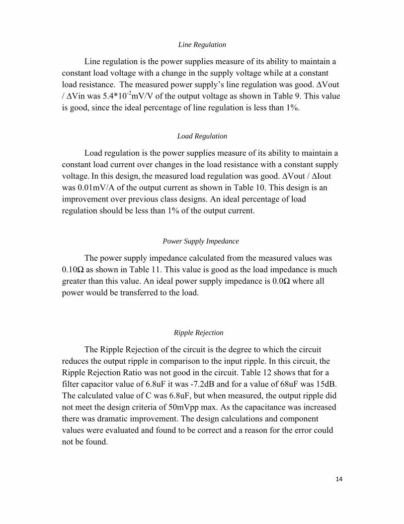
Line Regulation
Line regulation is the power supplies measure of its ability to maintain a constant load voltage with a change in the supply voltage while at a constant load resistance. The measured power supply’s line regulation was good. ∆Vout / ∆Vin was 5.4*10-2mV/V of the output voltage as shown in Table 9. This value is good, since the ideal percentage of line regulation is less than 1%.
Load Regulation
Load regulation is the power supplies measure of its ability to maintain a constant load current over changes in the load resistance with a constant supply voltage. In this design, the measured load regulation was good. ∆Vout / ∆Iout was 0.01mV/A of the output current as shown in Table 10. This design is an improvement over previous class designs. An ideal percentage of load regulation should be less than 1% of the output current. Power Supply Impedance
The power supply impedance calculated from the measured values was 0.10Ω as shown in Table 11. This value is good as the load impedance is much greater than this value. An ideal power supply impedance is 0.0Ω where all power would be transferred to the load.
Ripple Rejection
The Ripple Rejection of the circuit is the degree to which the circuit reduces the output ripple in comparison to the input ripple. In this circuit, the Ripple Rejection Ratio was not good in the circuit. Table 12 shows that for a filter capacitor value of 6.8uF it was -7.2dB and for a value of 68uF was 15dB. The calculated value of C was 6.8uF, but when measured, the output ripple did not meet the design criteria of 50mVpp max. As the capacitance was increased there was dramatic improvement. The design calculations and component values were evaluated and found to be correct and a reason for the error could not be found.

15
Efficiency
Efficiency is the ratio of Power Out to Power In of a circuit. A higher value means less power is lost due to heat and the circuit is more efficient. This design has a more efficient power transfer from input to output than previous linear power supply class designs. Table 13 shows that the measured power efficiency for 100% rated current (250mA) was 75.4% and for 50% (125mA) was 69.0%. Due to the design being more efficient, heat sinking of the pass transistor was not required.
Power Out is referring to the power dissipated by the load. The Power In is the total power consumed by the complete circuit. The individual component power dissipations are shown in Table 14. Based on the individual calculation, the total power dissipated in the circuit is 3.72 Watts. Using 3.72 Watts as the Power In, the efficiency becomes only 45.7% which does not appear to be a realistic number for a Switched Mode Power Supply.
Conclusion
This design met the design constraints of supplying 250mA to an 8.5VDC load. The load voltage remained constant at 8.5VDC until the short circuit current (ISC) was reached upon which it then went into hard current limiting mode. The output ripple was greater than previous class designs, but the trade off is improved circuit efficiency (74.5%). The increased efficiency also means a cooler running circuit and reduced component power ratings. Provided that the additional noise a Switch Mode Power Supply introduces to the load, it will produce less heat than a linear power supply.

0
0
1
1
2
2
3
3
4
4
5
5
6
6
7
7
8
8
A A
B B
C C
D D
E E
F F
G GET-3100 Electronic Circuit Design
Date: Sheet of
Rev:Size:
Design 4 Switch Mode Power Supply Schm
2011-05-01 1 1
1.0A
Milwaukee School of Engineering
Alex Kremnitzer
Notes:Unless specified:1. All resistors are carbon composition, 10%, 1/4W. .2. Capacitor C is electrolytic, 16WVDC.3. Capacitor C2 is ceramic, 20WVDC>
R5620Ω1/2W
R_17.5kΩ
R_22.7kΩ
Rpot
2kΩKey=A
50%
Rcs0.64Ω
C6.8µF
Cc1nF
(TIP32 SUBSTITUTE)
Rload100ΩKey=B10W
34%
Vunreg
17.5 V
HewlettPackardE3631A
QpMJE15033
D11N5818
L.001µH
R6420Ω
Rc51kΩ
Ct2.2nF
Rt13kΩR4
5.1kΩ
R35.1kΩ
SG3524
C2C1VCCVREFIN+
IN-
E1
E2CL-CL+
RT CT GND COMP
12 1311
145
4
9876
2
1
16 15