Agilent AN 1307 Testing CDMA Base Station Amplifiersmy.ece.ucsb.edu/York/Yorklab/Useful...
35
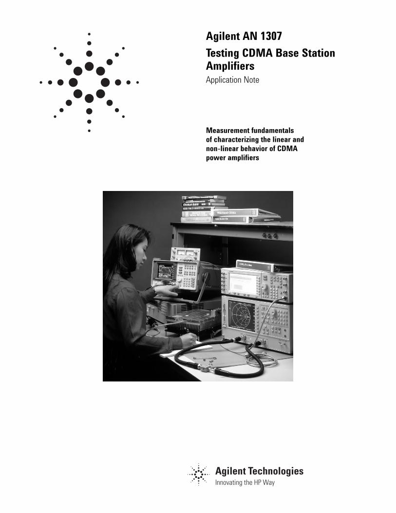
Agilent AN 1307 Testing CDMA Base Station Amplifiers Application Note Measurement fundamentals of characterizing the linear and non-linear behavior of CDMA power amplifiers
Transcript of Agilent AN 1307 Testing CDMA Base Station Amplifiersmy.ece.ucsb.edu/York/Yorklab/Useful...
Agilent AN 1307
Testing CDMA Base StationAmplifiersApplication Note
Measurement fundamentals of characterizing the linear and non-linear behavior of CDMA power amplifiers
45567
8889
10131415
1616171818192021222324252526262829293032
34
35
Table of Contents
Introduction1. Overview1.1 Amplifier measurements1.2 Power amplifier characteristics1.3 Common CDMA base station amplifier requirements
2. Test System Requirements2.1 Stimulus response measurements2.2 Network analyzer requirements2.3 High-power considerations2.4 Typical test setups2.5 Digital signal generator requirements2.6 Signal analyzer requirements2.7 Power meter requirements
3. Measurements and Test Instruments3.1 Pulsed RF and pulsed bias3.2 Load-pull analysis3.3 Network analysis
3.3.1 Transmission measurements3.3.1.1 Gain and flatness3.3.1.2 Phase3.3.1.3 Group delay3.3.1.4 Reverse isolation
3.3.2 Reflection measurements3.3.2.1 Return loss/SWR3.3.2.2 Input impedance3.3.2.3 Output impedance
3.4 In-channel measurements3.4.1 RF-channel output power3.4.2 Occupied bandwidth
3.5 Out-of-channel measurements3.5.1 Harmonic distortion3.5.2 Adjacent channel power ratio3.5.3 Spectral regrowth
4. Summary
5. References
4
This application note covers the testing needs andissues encountered in the development of CDMAhigh-power base station amplifiers.
The amplifier provides a fundamental function ofthe base station in a wireless communications sys-tem. The signal level must be amplified enough toovercome the inherent losses during wireless trans-mission so that it can be received by the mobiles.The design requirements for RF power amplifiersinclude high output power, high linearity, and goodefficiency.
CDMA systems are experiencing tremendousgrowth in the global communication marketplace.This growth is fueling many research programs and expanding the technology opportunities forall manufacturers. Coupled with this large growth
are some challenging measurement problems.
The objective of this application note is to coverthe basic measurement fundamentals of character-izing the linear and non-linear behavior of CDMApower amplifiers. In addition, it features some of the latest test solutions developed by AgilentTechnologies for design validation, and for manu-facturing test of CDMA base station amplifiers.
The overview begins by presenting power amplifiermeasurements, defining the characteristics ofpower amplifiers, and presenting specific CDMAamplifier requirements. Next, the different test system architectures that can be used for testingpower amplifiers are analyzed and the limitationsof each are discussed. A brief look at the require-ments for the individual pieces of test equipmentwill be presented as well.
The section “Measurements and Test Instruments”briefly covers amplifier testing under pulsed-RFand pulsed-bias conditions. This is often necessaryfor testing unpackaged devices that lack sufficientheatsinking to be run continuously. Also brieflyexplored is how load-pull analysis can be used tooptimize the design of a power amplifier. In thissame section, the more common measurements arecovered in more detail, starting with vector net-work analyzer-based transmission and reflectionmeasurements, which include both linear and non-linear tests. Additional non-linear measurementssuch as in- and out-of-channel measurements whichrequire a different set of test equipment, are pre-sented at the end of the section.
Introduction
5
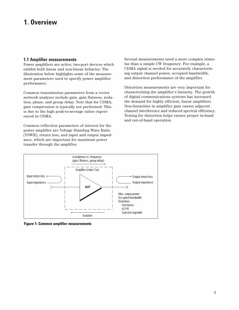
1.1 Amplifier measurementsPower amplifiers are active, two-port devices whichexhibit both linear and non-linear behavior. Theillustration below highlights some of the measure-ment parameters used to specify power amplifierperformance.
Common transmission parameters from a vectornetwork analyzer include gain, gain flatness, isola-tion, phase, and group delay. Note that for CDMA,gain compression is typically not performed. Thisis due to the high peak-to-average ratios experi-enced in CDMA.
Common reflection parameters of interest for thepower amplifier are Voltage Standing Wave Ratio(VSWR), return loss, and input and output imped-ance, which are important for maximum powertransfer through the amplifier.
Several measurements need a more complex stimu-lus than a simple CW frequency. For example, aCDMA signal is needed for accurately characteriz-ing output channel power, occupied bandwidth,and distortion performance of the amplifier.
Distortion measurements are very important forcharacterizing the amplifier’s linearity. The growthof digital communications systems has increasedthe demand for highly efficient, linear amplifiers.Non-linearities in amplifier gain causes adjacentchannel interference and reduced spectral efficiency.Testing for distortion helps ensure proper in-bandand out-of-band operation.
1. Overview
Figure 1: Common amplifier measurements
Output return loss
Output impedance
Input return loss
Input impedance
Isolation
Gain/phase vs. frequency(gain, flatness, group delay)
Max. output powerOccupied bandwidthDistortion: Harmonics ACPR Spectral regrowth
AUT
Amplifier Under Test
6
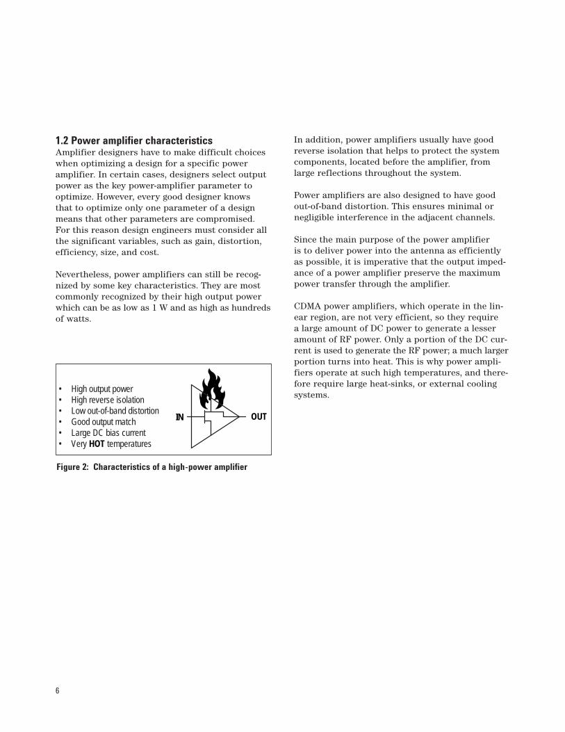
1.2 Power amplifier characteristicsAmplifier designers have to make difficult choiceswhen optimizing a design for a specific poweramplifier. In certain cases, designers select outputpower as the key power-amplifier parameter tooptimize. However, every good designer knows that to optimize only one parameter of a designmeans that other parameters are compromised.For this reason design engineers must consider allthe significant variables, such as gain, distortion,efficiency, size, and cost.
Nevertheless, power amplifiers can still be recog-nized by some key characteristics. They are mostcommonly recognized by their high output powerwhich can be as low as 1 W and as high as hundredsof watts.
In addition, power amplifiers usually have goodreverse isolation that helps to protect the systemcomponents, located before the amplifier, fromlarge reflections throughout the system.
Power amplifiers are also designed to have goodout-of-band distortion. This ensures minimal ornegligible interference in the adjacent channels.
Since the main purpose of the power amplifier is to deliver power into the antenna as efficientlyas possible, it is imperative that the output imped-ance of a power amplifier preserve the maximumpower transfer through the amplifier.
CDMA power amplifiers, which operate in the lin-ear region, are not very efficient, so they require a large amount of DC power to generate a lesseramount of RF power. Only a portion of the DC cur-rent is used to generate the RF power; a much largerportion turns into heat. This is why power ampli-fiers operate at such high temperatures, and there-fore require large heat-sinks, or external coolingsystems.
Figure 2: Characteristics of a high-power amplifier
• High output power• High reverse isolation• Low out-of-band distortion• Good output match• Large DC bias current• Very HOT temperatures
IN OUT
7
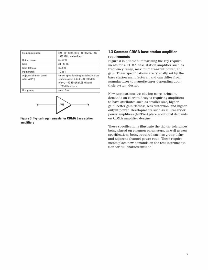
Figure 3: Typical requirements for CDMA base stationamplifiers
1.3 Common CDMA base station amplifierrequirementsFigure 3 is a table summarizing the key require-ments for a CDMA base station amplifier such asfrequency range, maximum transmit power, andgain. These specifications are typically set by thebase station manufacturer, and can differ frommanufacturer to manufacturer depending upontheir system design.
New applications are placing more stringentdemands on current designs requiring amplifiersto have attributes such as smaller size, higher gain, better gain flatness, less distortion, and higheroutput power. Developments such as multi-carrierpower amplifiers (MCPAs) place additional demandson CDMA amplifier designs.
These specifications illustrate the tighter tolerancesbeing placed on common parameters, as well as newspecifications being required such as group delayand adjacent-channel-power ratio. These require-ments place new demands on the test instrumenta-tion for full characterization.
AUT
Frequency ranges 824 - 894 MHz, 1810 - 1870 MHz, 1930 - 1990 MHz, and so forth.
Output power 8 - 45 W
Gain 30 - 40 dB
Gain flatness ±0.5 dB
Input match 1.2 to 1
Adjacent channel power ratio (ACPR)
vendor specific but typically better than system specs: < 45 dBc @ ±885 kHz offset, < 60 dBc @ ±1.98 kHz and ± 2.25 kHz offsets
Group delay 4 ns ±2 ns
8
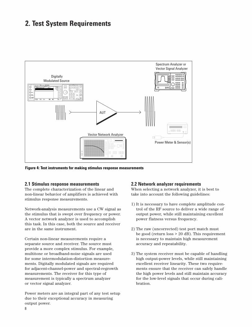
2.1 Stimulus response measurementsThe complete characterization of the linear andnon-linear behavior of amplifiers is achieved withstimulus response measurements.
Network-analysis measurements use a CW signal asthe stimulus that is swept over frequency or power.A vector network analyzer is used to accomplishthis task. In this case, both the source and receiverare in the same instrument.
Certain non-linear measurements require a separate source and receiver. The source must provide a more complex stimulus. For example,multitone or broadband-noise signals are used for some intermodulation-distortion measure-ments. Digitally modulated signals are required for adjacent-channel-power and spectral-regrowthmeasurements. The receiver for this type of measurement is typically a spectrum analyzer or vector signal analyzer.
Power meters are an integral part of any test setupdue to their exceptional accuracy in measuringoutput power.
2.2 Network analyzer requirementsWhen selecting a network analyzer, it is best totake into account the following guidelines:
1) It is necessary to have complete amplitude con-trol of the RF source to deliver a wide range ofoutput power, while still maintaining excellentpower flatness versus frequency.
2) The raw (uncorrected) test port match must be good (return loss > 20 dB). This requirementis necessary to maintain high measurementaccuracy and repeatability.
3) The system receiver must be capable of handlinghigh output-power levels, while still maintainingexcellent receiver linearity. These two require-ments ensure that the receiver can safely handlethe high power levels and still maintain accuracyfor the low-level signals that occur during cali-bration.
2. Test System Requirements
AUT
DigitallyModulated Source
Vector Network Analyzer
Spectrum Analyzer orVector Signal Analyzer
Power Meter & Sensor(s)
INPUT
I
Q
DATA
DATACLOCK
SYMBOLCLOCK
Preset Local More
More Inc.Set
MenusE4433B 250 kHz to 4.0 GHzESG-D SERIES DIGITAL SIGNAL GENERATOR
Real Time I/Qbaseband
Arb waveformGenerator
BERT
FREQUENCY
4.000 000 000 00 GHzAMPLITUDE
7.00 dBm
Figure 4: Test instruments for making stimulus response measurements
9
Another important consideration for testing ampli-fiers with network analyzers is the detector type.There are two basic modes of detection for networkanalyzers: broadband and narrowband. The broad-band mode uses diode detectors and does not pro-vide phase information. The narrowband mode usesa tuned receiver and does provide phase informa-tion. It also provides more dynamic range, less noise,and reduced sensitivity to measurement errorscaused by harmonic and other spurious signals.
When measuring CDMA base station amplifiers,narrowband mode should be used to achieve themost accurate and repeatable measurements.
2.3 High-power considerationsTesting high-power amplifiers is unique becausethe power levels needed for testing may be beyondthe measurement range of the test instruments.
Power amplifiers typically require high-input levelsin order to characterize them under conditionssimilar to actual operation. Similarly, the outputlevel is also large when tested close to actual oper-ating conditions.
Ensuring an appropriate input level and notexceeding the compression and damage level of the test instruments are the two main concernswhen testing high-power amplifiers:
To provide high-input power to the amplifier undertest (AUT), it is necessary to insert a booster ampli-fier in the input path. The booster amplifier shouldbe selected with enough gain and output power toboost the input signal to the desired level. It shouldalso be a very linear (Class A) amplifier, operatingin its linear region, so as not to contribute anyadditional signal distortion.
To reduce the high output-power level from theAUT to a level that can be safely handled by thetest equipment, it is required that an external high-power coupler or a high-power attenuator beinstalled at the output of the amplifier. Care shouldbe taken when selecting this component to ensurethat its power-handling capability is adequate.
10
To make accurate measurements, additional concerns or considerations include calibration and thermal issues:
The frequency-response effects of the attenuatorsand couplers must be considered since they arepart of the test system. It is important to selectcomponents that provide the best raw match possi-ble. Proper calibration techniques should be usedto remove or minimize the effects of the externalhardware in the system.
When calibrating the extra attenuation added afterthe amplifier, the input levels to the receiver maybe low during the calibration cycle. The power levelsmust be significantly above the noise floor of thereceiver for accurate measurements. Vector networkanalyzers are often used for high-power applicationssince their noise floor is typically <–90 dBm, andthey exhibit excellent receiver linearity over a widerange which also improves measurement accuracy.
Thermal considerations during the measurementshould also be considered for accurate measurements.For example, when testing high-power amplifiers,the load used on the output coupler must be ableto absorb the power delivered by the amplifierunder test. Most loads designed for small-signaluse can only handle up to about one watt of power.Beyond that, special loads that can dissipate morepower must be used. The temperature of the loadshould be allowed to stabilize if its impedancecharacteristics change significantly versus temper-ature. The amplifier itself may behave very differ-ently at various temperatures, so the tests shouldbe done when the amplifier is at the desired oper-ating temperature.
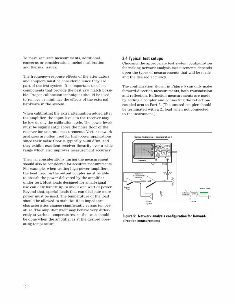
2.4 Typical test setupsChoosing the appropriate test system configurationfor making network analysis measurements dependsupon the types of measurements that will be madeand the desired accuracy.
The configuration shown in Figure 5 can only makeforward-direction measurements, both transmissionand reflection. Reflection measurements are madeby adding a coupler and connecting the reflection-coupled arm to Port 2. (The unused coupler shouldbe terminated with a Zo load when not connectedto the instrument.)
Network Analysis - Configuration 1
BoosterAmp
H
ACTIVE CHANNEL
RESPONSE
STIMULUS
ENTRY
INSTRUMENT STATE R CHANNEL
R L T S
HP-IB STATUS
8753DNETWORK ANALYZER
30 KHz-3GHz
PROBE POWER FUSED
AUT
Ref In
Reflection measurements
to Port 2
To network analyzer GPIB
PowerSplitter
Power Meter
Sensor
Port 2Port 1
Figure 5: Network analysis configuration for forward-direction measurements
11
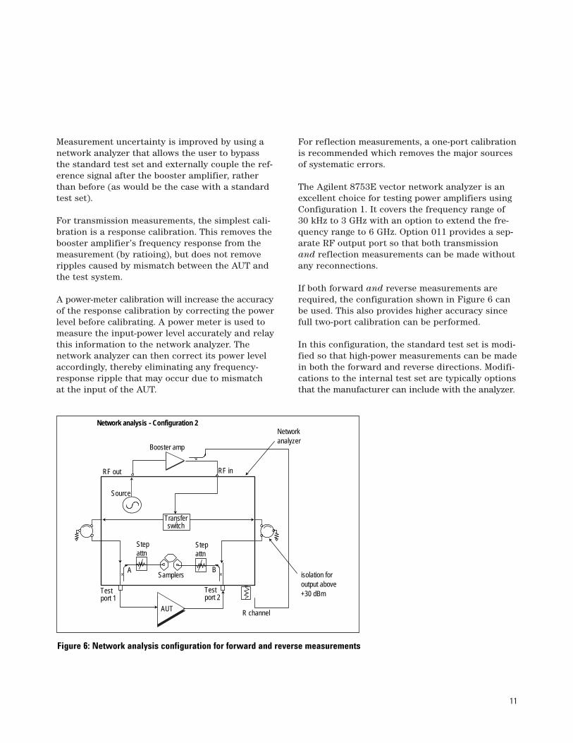
Measurement uncertainty is improved by using anetwork analyzer that allows the user to bypassthe standard test set and externally couple the ref-erence signal after the booster amplifier, ratherthan before (as would be the case with a standardtest set).
For transmission measurements, the simplest cali-bration is a response calibration. This removes thebooster amplifier’s frequency response from themeasurement (by ratioing), but does not removeripples caused by mismatch between the AUT andthe test system.
A power-meter calibration will increase the accuracyof the response calibration by correcting the powerlevel before calibrating. A power meter is used tomeasure the input-power level accurately and relaythis information to the network analyzer. The network analyzer can then correct its power levelaccordingly, thereby eliminating any frequency-response ripple that may occur due to mismatch at the input of the AUT.
For reflection measurements, a one-port calibrationis recommended which removes the major sourcesof systematic errors.
The Agilent 8753E vector network analyzer is an excellent choice for testing power amplifiers usingConfiguration 1. It covers the frequency range of30 kHz to 3 GHz with an option to extend the fre-quency range to 6 GHz. Option 011 provides a sep-arate RF output port so that both transmissionand reflection measurements can be made withoutany reconnections.
If both forward and reverse measurements arerequired, the configuration shown in Figure 6 canbe used. This also provides higher accuracy sincefull two-port calibration can be performed.
In this configuration, the standard test set is modi-fied so that high-power measurements can be madein both the forward and reverse directions. Modifi-cations to the internal test set are typically optionsthat the manufacturer can include with the analyzer.
Network analysis - Configuration 2
Booster amp
AUT
Source
Samplers
RF out RF in
R channel
Testport 1
Testport 2
Stepattn
isolation for output above +30 dBm
Network analyzer
A B
Stepattn
Transferswitch
Figure 6: Network analysis configuration for forward and reverse measurements
12
Features that allow reverse direction and higherpower levels to be measured include:
1) Access to the RF path between the source andthe transfer switch. This allows the source signalto be amplified and then switched between Port1 or Port 2. Forward and reverse high-powermeasurements can now be made.
2) Direct access to the R, or reference channel asin the first configuration, allowing for improvedaccuracy.
3) Direct access to the RF path between the trans-fer switch and the test ports. This allows addi-tion of high-power isolators to protect the transfer switch.
4) Step attenuators between the couplers and thesamplers on the A and B channels. These reducethe signal to an optimum level for the receiver.
The Agilent 8720D family of vector network analyz-ers with Option 085 is ideal for making both reflec-tion and transmission measurements in the forwardand reverse directions without having to make multi-ple AUT connections. It is tailored for testing poweramplifiers using Configuration 2, and covers thefrequency range of 50 MHz to 13.5, 20, or 40 GHz.1
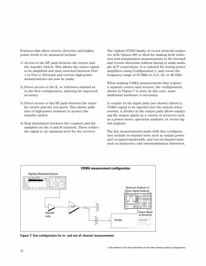
When making CDMA measurements that require a separate source and receiver, the configurationshown in Figure 7 is used. In this case, some additional hardware is necessary.
A coupler in the input path (not shown) allows aCDMA signal to be injected into the system whenneeded. A divider in the output path allows analyz-ing the output signal on a variety of receivers suchas a power meter, spectrum analyzer, or vector sig-nal analyzer.
The key measurements made with this configura-tion include in-channel tests such as output powerand occupied bandwidth, and out-of-channel testssuch as harmonics and intermodulation distortion.
Figure 7: Test configuration for in- and out-of-channel measurements
CDMA measurement configuration
Boosteramp
Divider
AUT
Digitally Modulated Source
Spectrum Analyzer orVector Signal Analyzer
Power Meter & Sensor(s)
INPUT
I
Q
DATA
DATACLOCK
SYMBOLCLOCK
Preset Local More
More Inc.Set
MenusE4433B 250 kHz to 4.0 GHzESG-D SERIES DIGITAL SIGNAL GENERATOR
Real Time I/Qbaseband
Arb waveformGenerator
BERT
FREQUENCY
4.000 000 000 00 GHzAMPLITUDE
7.00 dBm
1. See reference 3 for more information on the other network analysis configurations.
13
2.5 Digital signal generator requirementsWhen choosing a CDMA signal generator, there are several requirements to consider. Ensuring coverage of the frequency range of the amplifier is, of course, the first requirement.
When making in-channel tests, the key requirementfor the signal generator is waveform quality. Thisensures a spectrally correct CDMA signal withinthe 1.23 MHz channel bandwidth.
When making out-of-channel tests, the key require-ment for the signal generator is that it has excellentadjacent-channel-power performance. In order tomeet the stringent spectral-regrowth specificationsplaced on CDMA power amplifiers, it is importantto ensure that the signal generator is not contribut-ing any adjacent-channel interference to the meas-urement.
In order to test the amplifier under real-world con-ditions, the signal generator must provide a realis-tic CDMA signal. The specification in IS-97 statesthat an appropriate signal for emulating real-worldCDMA includes one pilot, sync, and paging channeland six traffic channels with specified power levels.Depending upon the data and specific traffic chan-nels selected, this can provide a signal with a crestfactor of up to 14 -15 dB.1 A generator which allowsselection of different Walsh-coded channels, powerlevels, and data is important for fully characteriz-ing the base station amplifier.
The Agilent ESG-series digital signal generatorsoffer an excellent source for CDMA base stationamplifer testing. These sources provide pre-loadedwaveforms which simplify CDMA signal generation.For example, the specified 9-channel waveformwith pilot, paging, sync, and 6 traffic channels isalready pre-loaded into the generator. In addition,precise signal statistics, such as individual Walsh-coded channel-power levels, can be generated tooptimize measurement accuracy.
Another CDMA signal generator available fromAgilent is the Multi-Format Communications SignalSimulator (MCSS). This is a more versatile solu-tion, offering multicarriers (both CW and digitallymodulated signals), as well as noise-power ratio(NPR) measurements for use in testing multicarrieramplifiers (MCPAs).
1. See reference 1 for a detailed discussion on how the crest factor, or peak-to-average ratio, affects distortion measurements.
14
2.6 Signal analyzer requirementsAs with the digital signal generator, the mostimportant requirements for the signal analyzer are frequency range and performance. Accuracy,repeatability, and dynamic range are the key performance parameters.
The ability of the analyzer to measure the adjacent-channel power or spectral regrowth is determinedby its dynamic-range performance. IS-95 CDMAsystem requirements, using a 30 kHz resolutionbandwidth, are –45 dBc at ± 885 kHz offset and–60 dBc at ± 1.98 kHz offset. Base station amplifierspecifications will be better than this.
It can also be very important, even in R&D, thatthe measurements be fast and easy to make. Thisallows the R&D engineer to focus on his or heramplifier design rather than the test equipmentand measurement details. Downloadable softwareprograms provided for the analyzers can makecomplicated CDMA measurements much easier and do not require the user to write his or her own programs.
An analyzer with the flexibility to change parame-ters such as integration bandwidths, mask limits,or frequency offsets can allow for testing a varietyof amplifier designs. Analyzers with sophisticatederror and signal quality analysis capabilities maketroubleshooting quick and easy.
Agilent spectrum analyzers that can be used tomake in- and out-of-channel measurements includethe Agilent 8590 E-series and 8560 E-series. The8590 E-series spectrum analyzer has a measure-ment personality available specifically for CDMA,providing one-button measurements (85725C). Ifhigher performance is required, the 8560 E-seriesspectrum analyzer provides higher dynamic range,lower noise floor, and better accuracy than the8590 E-series. These analyzers require manual (orcontrol through external PC) power calculationsand settings.
For the highest versatility in the R&D environment,the Agilent 89441A provides numerous error and signal-quality-analysis results needed for trouble-shooting amplifier designs.
15
2.7 Power meter requirementsThe requirements for the power meter and sensors are fairly straightforward. Frequencyrange that covers both cellular and PCS CDMA is the first concern.
For high-power amplifiers, it is also important that the power sensor has the appropriate power-measurement range for the amplifier’s expectedoutput power.
In terms of power accuracy, a power meter has the best performance of any other test equipment.It is also necessary for improving accuracy forsome network-analysis measurements.
Using a dual-sensor power meter allows monitoringboth the input and output power of the amplifierunder test. This gives you the ability to make CDMAgain measurements (as opposed to CW gain meas-urements made with a network analyzer) by ratioingthe input and output power.
Depending upon which sensor is used, the AgilentEPM 442A dual-channel power meter can measurefrom –70 dBm to +44 dBm at frequencies from 100 kHz to 110 GHz. The Agilent ECP E18A powersensor has a wide dynamic range (–70 dBm to +20 dBm) over the frequency range of 10 MHz to18 GHz.
16
Now that you have read about the basic test-systemarchitectures and the requirements for the variouspieces of test equipment, the actual measurementsmade on CDMA base station amplifiers will be presented. In addition to describing the measure-ments, included is a brief description of some ofthe Agilent Technologies test equipment that canbe used.
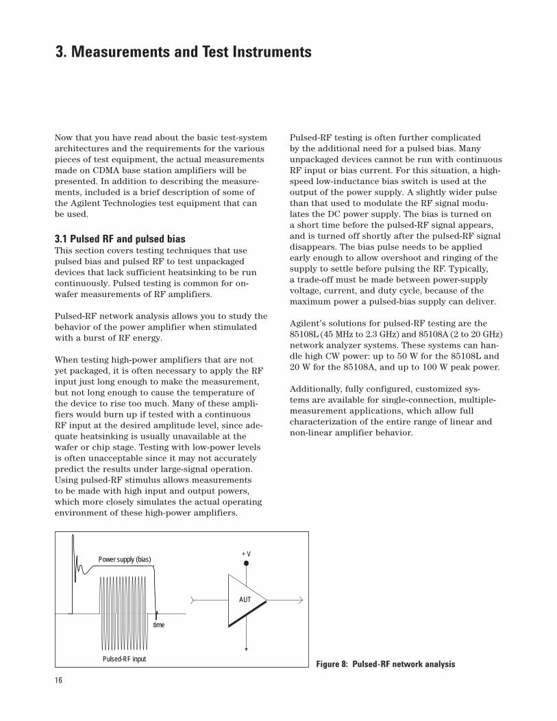
3.1 Pulsed RF and pulsed biasThis section covers testing techniques that usepulsed bias and pulsed RF to test unpackageddevices that lack sufficient heatsinking to be runcontinuously. Pulsed testing is common for on-wafer measurements of RF amplifiers.
Pulsed-RF network analysis allows you to study thebehavior of the power amplifier when stimulatedwith a burst of RF energy.
When testing high-power amplifiers that are notyet packaged, it is often necessary to apply the RFinput just long enough to make the measurement,but not long enough to cause the temperature ofthe device to rise too much. Many of these ampli-fiers would burn up if tested with a continuous RF input at the desired amplitude level, since ade-quate heatsinking is usually unavailable at thewafer or chip stage. Testing with low-power levelsis often unacceptable since it may not accuratelypredict the results under large-signal operation.Using pulsed-RF stimulus allows measurements to be made with high input and output powers,which more closely simulates the actual operatingenvironment of these high-power amplifiers.
Pulsed-RF testing is often further complicated by the additional need for a pulsed bias. Manyunpackaged devices cannot be run with continuousRF input or bias current. For this situation, a high-speed low-inductance bias switch is used at theoutput of the power supply. A slightly wider pulsethan that used to modulate the RF signal modu-lates the DC power supply. The bias is turned on a short time before the pulsed-RF signal appears,and is turned off shortly after the pulsed-RF signaldisappears. The bias pulse needs to be appliedearly enough to allow overshoot and ringing of thesupply to settle before pulsing the RF. Typically, a trade-off must be made between power-supplyvoltage, current, and duty cycle, because of themaximum power a pulsed-bias supply can deliver.
Agilent’s solutions for pulsed-RF testing are the85108L (45 MHz to 2.3 GHz) and 85108A (2 to 20 GHz)network analyzer systems. These systems can han-dle high CW power: up to 50 W for the 85108L and20 W for the 85108A, and up to 100 W peak power.
Additionally, fully configured, customized sys-tems are available for single-connection, multiple-measurement applications, which allow full characterization of the entire range of linear andnon-linear amplifier behavior.
3. Measurements and Test Instruments
Figure 8: Pulsed-RF network analysis
Power supply (bias)
Pulsed-RF input
time
AUT
+ V
17
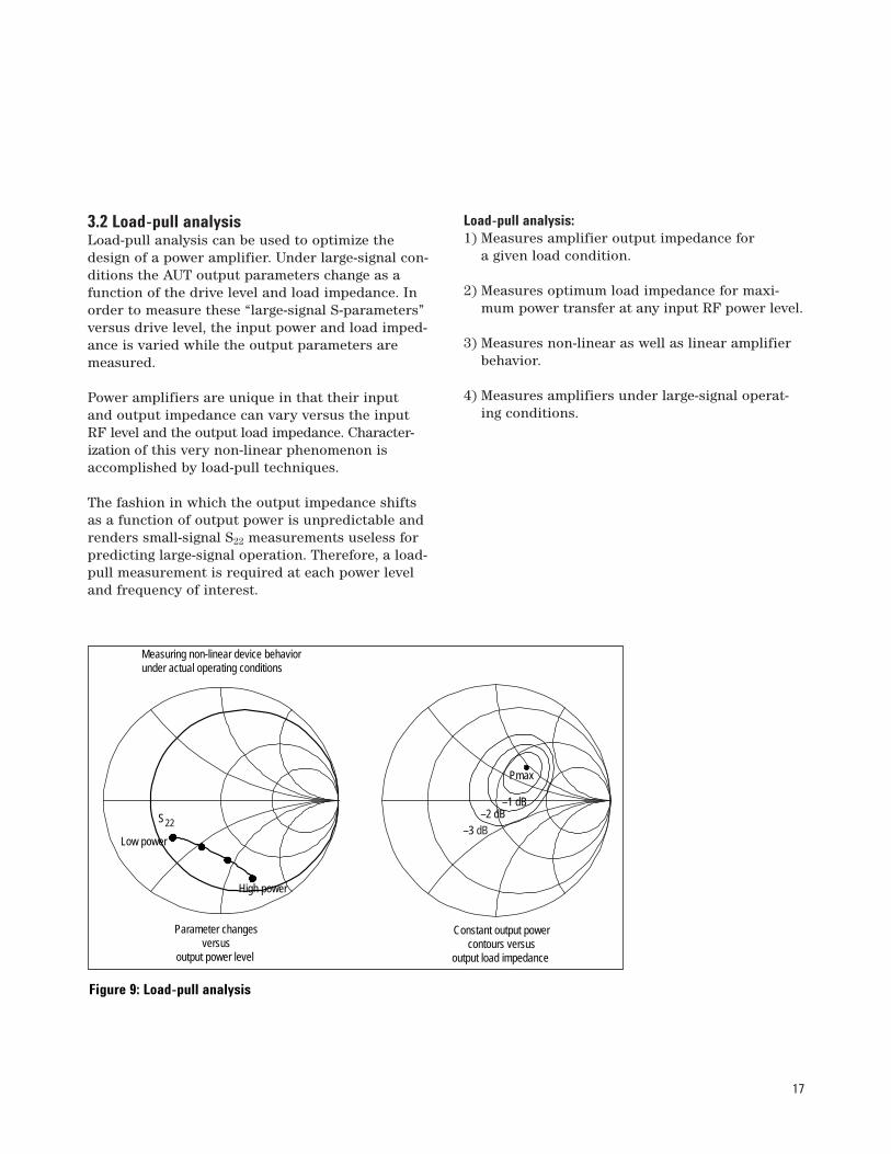
3.2 Load-pull analysisLoad-pull analysis can be used to optimize thedesign of a power amplifier. Under large-signal con-ditions the AUT output parameters change as afunction of the drive level and load impedance. Inorder to measure these “large-signal S-parameters”versus drive level, the input power and load imped-ance is varied while the output parameters aremeasured.
Power amplifiers are unique in that their input and output impedance can vary versus the inputRF level and the output load impedance. Character-ization of this very non-linear phenomenon isaccomplished by load-pull techniques.
The fashion in which the output impedance shiftsas a function of output power is unpredictable andrenders small-signal S22 measurements useless forpredicting large-signal operation. Therefore, a load-pull measurement is required at each power leveland frequency of interest.
Load-pull analysis:1) Measures amplifier output impedance for
a given load condition.
2) Measures optimum load impedance for maxi-mum power transfer at any input RF power level.
3) Measures non-linear as well as linear amplifierbehavior.
4) Measures amplifiers under large-signal operat-ing conditions.
Measuring non-linear device behaviorunder actual operating conditions
Low power
High power
S 22
Constant output powercontours versus
output load impedance
Pmax
–1 dB–2 dB
–3 dB
Parameter changesversus
output power level
Figure 9: Load-pull analysis
18
The most common result of a load-pull measure-ment is a series of constant output-power contours(not always circular), plotted on a Smith chartwhich represent all possible output impedances. A load-pull measurement is required at each powerlevel and frequency of interest, since the outputcontours are sensitive to these variables for mosthigh-power amplifiers. The output-power contoursshown are with a constant input power level andfrequency.
With the many measurements to be made, it isimportant that a load-pull-measurement system beeasily configured and provide fast measurements.
Agilent Technologies and ATN Microwave, Inc. have teamed to develop several load-pull systemswhich are completely integrated and specified to support large- and small-signal characterization.Fully configured turn-key systems offer the ulti-mate in ease-of-use and performance.
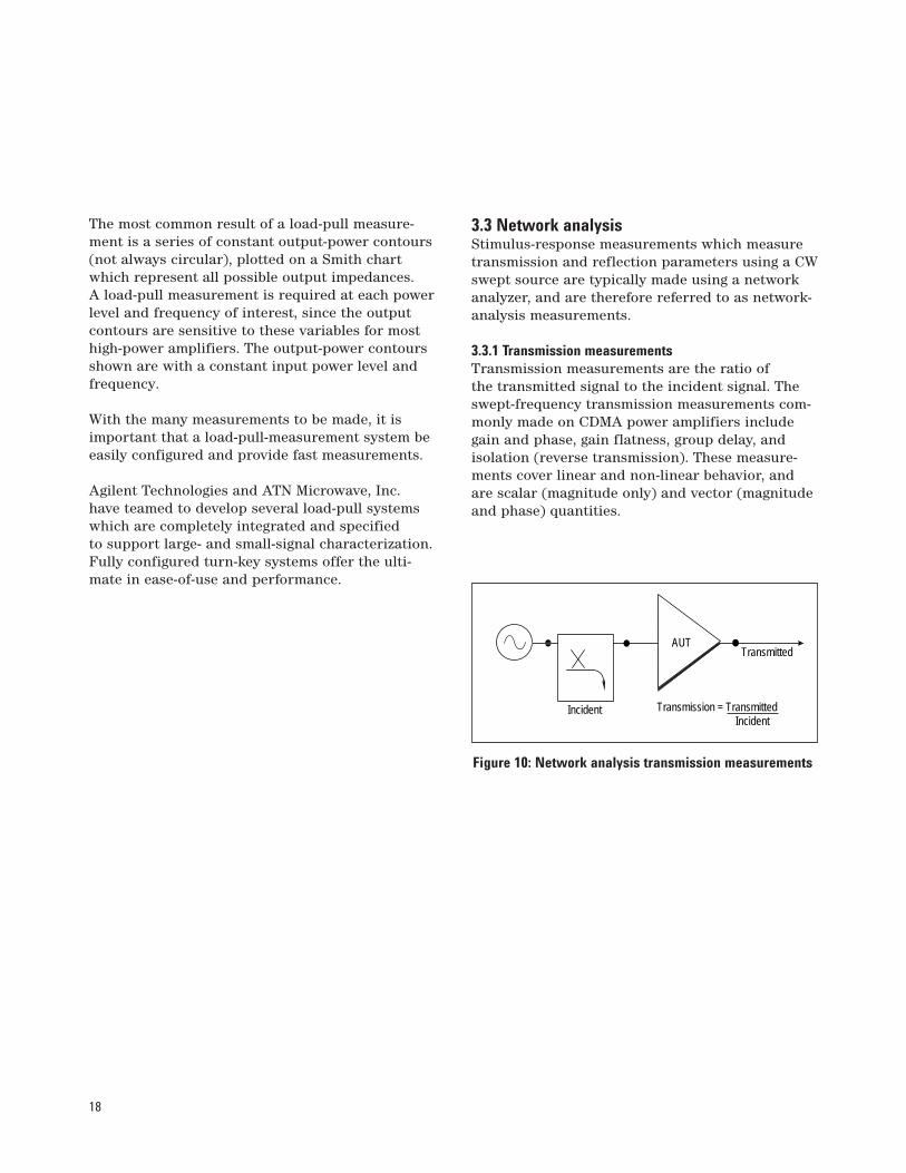
3.3 Network analysisStimulus-response measurements which measuretransmission and reflection parameters using a CWswept source are typically made using a networkanalyzer, and are therefore referred to as network-analysis measurements.
3.3.1 Transmission measurementsTransmission measurements are the ratio of the transmitted signal to the incident signal. Theswept-frequency transmission measurements com-monly made on CDMA power amplifiers includegain and phase, gain flatness, group delay, and isolation (reverse transmission). These measure-ments cover linear and non-linear behavior, andare scalar (magnitude only) and vector (magnitudeand phase) quantities.
Figure 10: Network analysis transmission measurements
Incident
TransmittedAUT
Transmission = Transmitted Incident
19
3.3.1.1 Gain and flatnessRF amplifier gain is defined as the ratio of the out-put power an amplifier delivers to a Zo load, to theinput power delivered from a Zo source, where Zo isthe characteristic impedance of the system. UsingS-parameter terminology, this is called S21.
Gain can be calculated as the difference betweenthe output and input power levels when they areexpressed in logarithmic terms such as dB.
Amplifier gain is most commonly specified as aminimum value over a specified frequency range,assuming that input and output signals are in theamplifier’s linear operating range. Since variationsin the frequency response of the amplifier cancause signal distortion, gain flatness is often speci-fied as how much the gain varies over the specifiedfrequency range.
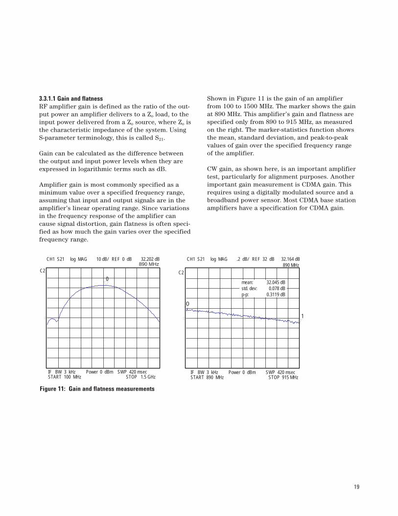
Shown in Figure 11 is the gain of an amplifier from 100 to 1500 MHz. The marker shows the gainat 890 MHz. This amplifier’s gain and flatness arespecified only from 890 to 915 MHz, as measuredon the right. The marker-statistics function showsthe mean, standard deviation, and peak-to-peakvalues of gain over the specified frequency range of the amplifier.
CW gain, as shown here, is an important amplifiertest, particularly for alignment purposes. Anotherimportant gain measurement is CDMA gain. Thisrequires using a digitally modulated source and abroadband power sensor. Most CDMA base stationamplifiers have a specification for CDMA gain.
Figure 11: Gain and flatness measurements
CH1 S21 log MAG 10 dB/ REF 0 dB 32.202 dB890 MHz
C2
IF BW 3 kHz Power 0 dBm SWP 420 msecSTART 100 MHz STOP 1.5 GHz
0
IF BW 3 kHz Power 0 dBm SWP 420 msecSTART 890 MHz STOP 915 MHz
CH1 S21 log MAG .2 dB/ REF 32 dB 32.164 dB890 MHz
C2
1
0
mean: 32.045 dBstd. dev: 0.078 dBp-p: 0.3119 dB
20
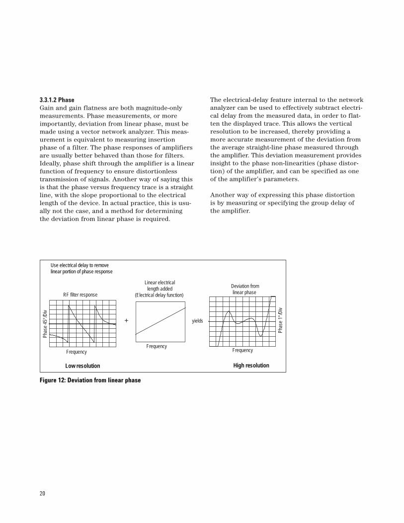
3.3.1.2 PhaseGain and gain flatness are both magnitude-onlymeasurements. Phase measurements, or moreimportantly, deviation from linear phase, must bemade using a vector network analyzer. This meas-urement is equivalent to measuring insertionphase of a filter. The phase responses of amplifiersare usually better behaved than those for filters.Ideally, phase shift through the amplifier is a linearfunction of frequency to ensure distortionlesstransmission of signals. Another way of saying thisis that the phase versus frequency trace is a straightline, with the slope proportional to the electricallength of the device. In actual practice, this is usu-ally not the case, and a method for determining the deviation from linear phase is required.
The electrical-delay feature internal to the networkanalyzer can be used to effectively subtract electri-cal delay from the measured data, in order to flat-ten the displayed trace. This allows the verticalresolution to be increased, thereby providing amore accurate measurement of the deviation fromthe average straight-line phase measured throughthe amplifier. This deviation measurement providesinsight to the phase non-linearities (phase distor-tion) of the amplifier, and can be specified as oneof the amplifier’s parameters.
Another way of expressing this phase distortion is by measuring or specifying the group delay ofthe amplifier.
Use electrical delay to removelinear portion of phase response
Linear electricallength added
(Electrical delay function)
+ yields
FrequencyFrequency
RF filter response
Deviation fromlinear phase
Phas
e 1°
/Div
Phas
e 45
°/Div
Frequency
Low resolution High resolution
Figure 12: Deviation from linear phase
21
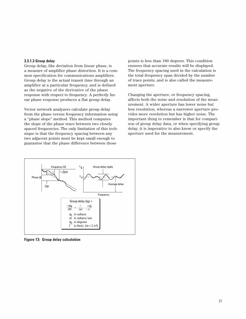
3.3.1.3 Group delayGroup delay, like deviation from linear phase, is a measure of amplifier phase distortion. It is a com-mon specification for communications amplifiers.Group delay is the actual transit time through anamplifier at a particular frequency, and is definedas the negative of the derivative of the phaseresponse with respect to frequency. A perfectly lin-ear phase response produces a flat group delay.
Vector network analyzers calculate group delayfrom the phase versus frequency information usinga “phase slope” method. This method computes the slope of the phase trace between two closelyspaced frequencies. The only limitation of this tech-nique is that the frequency spacing between anytwo adjacent points must be kept small enough toguarantee that the phase difference between those
points is less than 180 degrees. This conditionensures that accurate results will be displayed. The frequency spacing used in the calculation isthe total frequency span divided by the number of trace points, and is also called the measure-ment aperture.
Changing the aperture, or frequency spacing,affects both the noise and resolution of the meas-urement. A wider aperture has lower noise but less resolution, whereas a narrower aperture pro-vides more resolution but has higher noise. Theimportant thing to remember is that for compari-son of group delay data, or when specifying groupdelay, it is imperative to also know or specify theaperture used for the measurement.
Figure 13: Group delay calculation
φ1 in radiansω in radians/secφ2 in degreesf in Hertz (ω = 2 π f)
Group delay (tg) =
−dφ1
dω =
-1
360°d φd f*
Frequency
Group delay ripple
Average delay
t o
tg
Phase φ
∆φ
∆ωFrequency ω
2
22
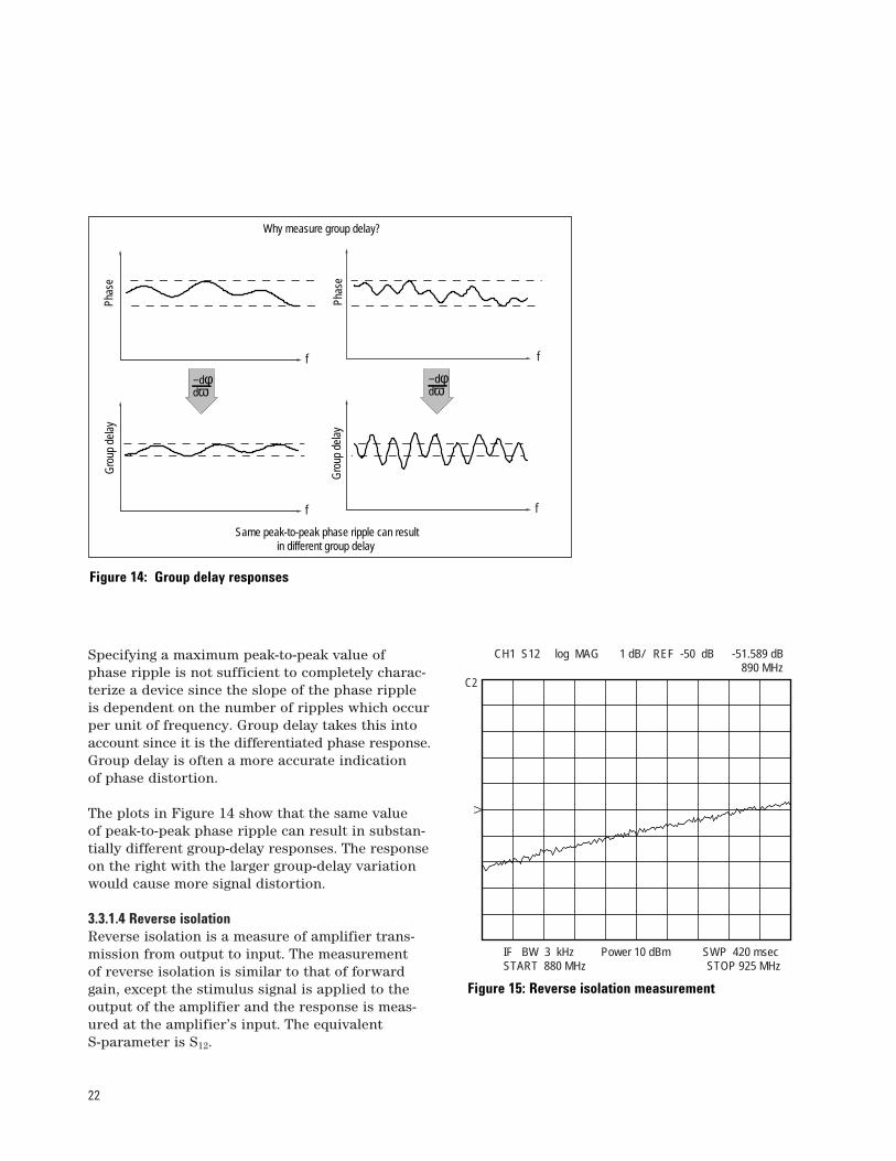
Specifying a maximum peak-to-peak value of phase ripple is not sufficient to completely charac-terize a device since the slope of the phase rippleis dependent on the number of ripples which occurper unit of frequency. Group delay takes this intoaccount since it is the differentiated phase response.Group delay is often a more accurate indication of phase distortion.
The plots in Figure 14 show that the same value of peak-to-peak phase ripple can result in substan-tially different group-delay responses. The responseon the right with the larger group-delay variationwould cause more signal distortion.
3.3.1.4 Reverse isolationReverse isolation is a measure of amplifier trans-mission from output to input. The measurement of reverse isolation is similar to that of forwardgain, except the stimulus signal is applied to theoutput of the amplifier and the response is meas-ured at the amplifier’s input. The equivalent S-parameter is S12.
Figure 14: Group delay responses
Why measure group delay?
Same peak-to-peak phase ripple can resultin different group delay
Phas
e
Phas
e
Gro
up d
elay
−dφdω
f
f
f
f
−dφdω
Gro
up d
elay
IF BW 3 kHz Power 10 dBm SWP 420 msecSTART 880 MHz STOP 925 MHz
CH1 S12 log MAG 1 dB/ REF -50 dB -51.589 dB 890 MHz
C2
Figure 15: Reverse isolation measurement
23
When using a network analyzer with a transmission/reflection test set for measuring reverse isolation,the amplifier must be disconnected and physicallyturned around so that the stimulus from the sourceport is applied to the amplifier’s output. If an S-parameter test set is used, the test set will switchthe stimulus to the second port, eliminating theneed to disconnect and reverse the amplifier.
There are several things that can be done to improvethe accuracy of an isolation measurement. Sinceamplifiers generally exhibit loss in the reverse direc-tion, there is no need for any attenuation that mayhave been used to protect the receiver during for-ward transmission measurements. Removing theattenuation will increase the dynamic range andhence the accuracy of the measurement, but a newresponse calibration should be done for maximumaccuracy. The RF source power can also be increasedto provide more dynamic range and accuracy. Notethat with the attenuation removed and the RF sourcepower increased, a forward sweep cannot be done.Reducing IF bandwidth or using averaging alsoimproves measurement accuracy, at the expense of measurement speed.
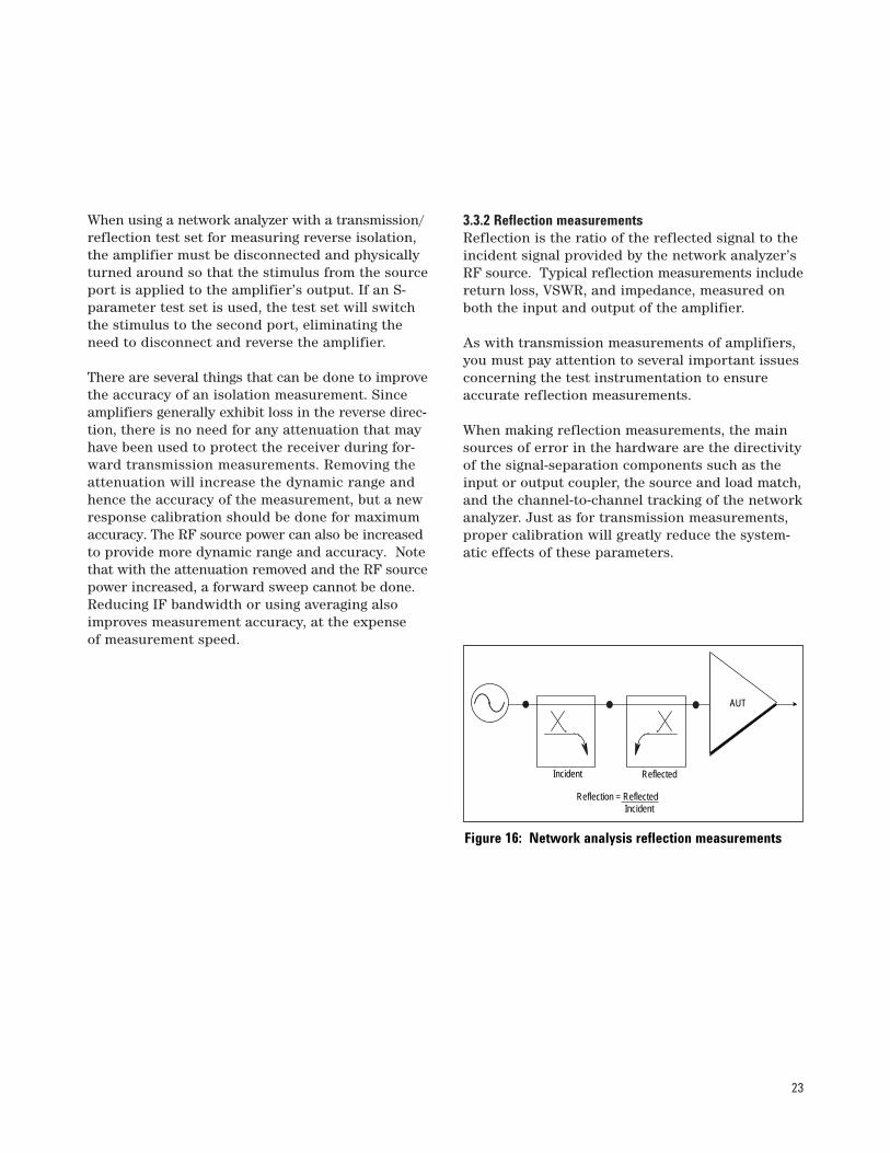
3.3.2 Reflection measurementsReflection is the ratio of the reflected signal to theincident signal provided by the network analyzer’sRF source. Typical reflection measurements includereturn loss, VSWR, and impedance, measured onboth the input and output of the amplifier.
As with transmission measurements of amplifiers,you must pay attention to several important issuesconcerning the test instrumentation to ensureaccurate reflection measurements.
When making reflection measurements, the mainsources of error in the hardware are the directivityof the signal-separation components such as theinput or output coupler, the source and load match,and the channel-to-channel tracking of the networkanalyzer. Just as for transmission measurements,proper calibration will greatly reduce the system-atic effects of these parameters.
Reflection = ReflectedIncident
AUT
Incident Reflected
Figure 16: Network analysis reflection measurements
24
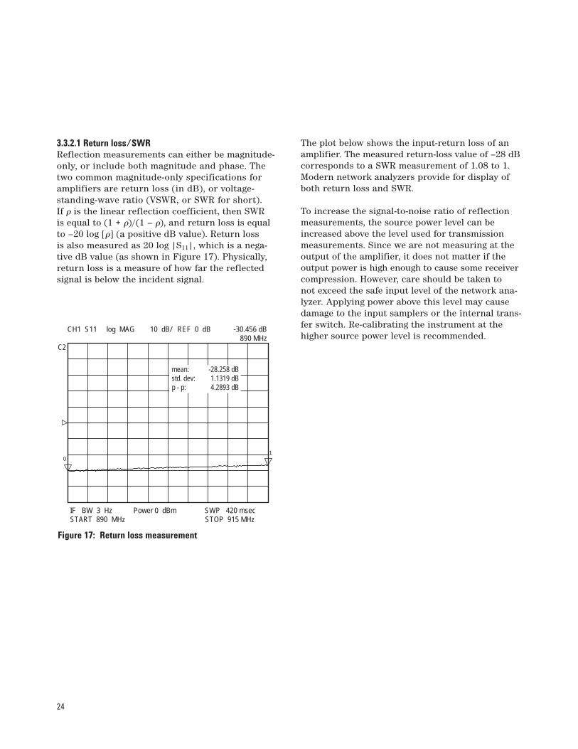
3.3.2.1 Return loss/SWRReflection measurements can either be magnitude-only, or include both magnitude and phase. Thetwo common magnitude-only specifications foramplifiers are return loss (in dB), or voltage-standing-wave ratio (VSWR, or SWR for short). If r is the linear reflection coefficient, then SWR is equal to (1 + r)/(1 – r), and return loss is equalto –20 log [r] (a positive dB value). Return loss is also measured as 20 log |S11|, which is a nega-tive dB value (as shown in Figure 17). Physically,return loss is a measure of how far the reflectedsignal is below the incident signal.
The plot below shows the input-return loss of anamplifier. The measured return-loss value of –28 dBcorresponds to a SWR measurement of 1.08 to 1.Modern network analyzers provide for display ofboth return loss and SWR.
To increase the signal-to-noise ratio of reflectionmeasurements, the source power level can beincreased above the level used for transmissionmeasurements. Since we are not measuring at theoutput of the amplifier, it does not matter if theoutput power is high enough to cause some receivercompression. However, care should be taken to not exceed the safe input level of the network ana-lyzer. Applying power above this level may causedamage to the input samplers or the internal trans-fer switch. Re-calibrating the instrument at thehigher source power level is recommended.
Figure 17: Return loss measurement
CH1 S11 log MAG 10 dB/ REF 0 dB -30.456 dB 890 MHz
C2
IF BW 3 Hz Power 0 dBm SWP 420 msec START 890 MHz STOP 915 MHz
10
mean: -28.258 dBstd. dev: 1.1319 dBp - p: 4.2893 dB
25
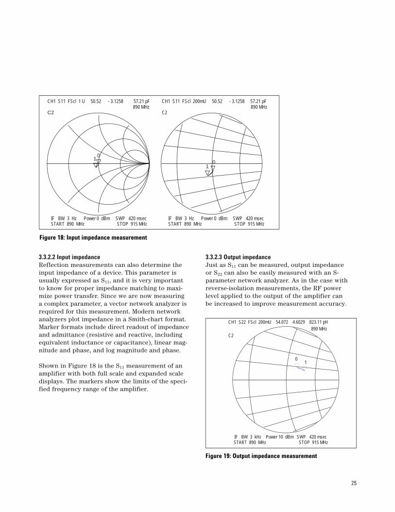
3.3.2.2 Input impedanceReflection measurements can also determine theinput impedance of a device. This parameter isusually expressed as S11, and it is very importantto know for proper impedance matching to maxi-mize power transfer. Since we are now measuring a complex parameter, a vector network analyzer isrequired for this measurement. Modern networkanalyzers plot impedance in a Smith-chart format.Marker formats include direct readout of impedanceand admittance (resistive and reactive, includingequivalent inductance or capacitance), linear mag-nitude and phase, and log magnitude and phase.
Shown in Figure 18 is the S11 measurement of anamplifier with both full scale and expanded scaledisplays. The markers show the limits of the speci-fied frequency range of the amplifier.
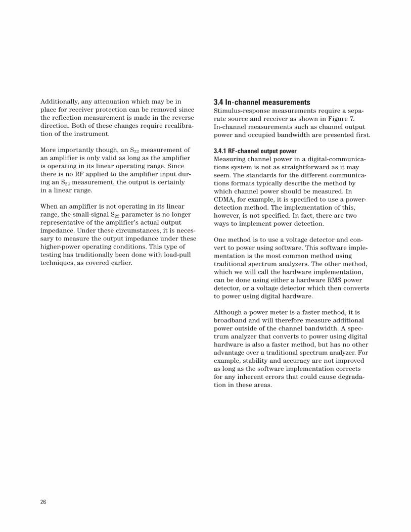
3.3.2.3 Output impedanceJust as S11 can be measured, output impedance or S22 can also be easily measured with an S-parameter network analyzer. As in the case withreverse-isolation measurements, the RF power level applied to the output of the amplifier can be increased to improve measurement accuracy.
CH1 S11 FScl 1 U 50.52 - 3.1258 57.21 pF 890 MHzC2
10
IF BW 3 Hz Power 0 dBm SWP 420 msecSTART 890 MHz STOP 915 MHz
IF BW 3 Hz Power 0 dBm SWP 420 msecSTART 890 MHz STOP 915 MHz
10
CH1 S11 FScl 200mU 50.52 - 3.1258 57.21 pF 890 MHzC2
Figure 18: Input impedance measurement
Figure 19: Output impedance measurement
10
IF BW 3 kHz Power 10 dBm SWP 420 msecSTART 890 MHz STOP 915 MHz
CH1 S22 FScl 200mU 54.072 4.6029 823.11 pH 890 MHzC2
26
Additionally, any attenuation which may be inplace for receiver protection can be removed sincethe reflection measurement is made in the reversedirection. Both of these changes require recalibra-tion of the instrument.
More importantly though, an S22 measurement ofan amplifier is only valid as long as the amplifier is operating in its linear operating range. Sincethere is no RF applied to the amplifier input dur-ing an S22 measurement, the output is certainly in a linear range.
When an amplifier is not operating in its linearrange, the small-signal S22 parameter is no longerrepresentative of the amplifier’s actual outputimpedance. Under these circumstances, it is neces-sary to measure the output impedance under thesehigher-power operating conditions. This type oftesting has traditionally been done with load-pulltechniques, as covered earlier.
3.4 In-channel measurementsStimulus-response measurements require a sepa-rate source and receiver as shown in Figure 7. In-channel measurements such as channel outputpower and occupied bandwidth are presented first.
3.4.1 RF-channel output powerMeasuring channel power in a digital-communica-tions system is not as straightforward as it mayseem. The standards for the different communica-tions formats typically describe the method bywhich channel power should be measured. InCDMA, for example, it is specified to use a power-detection method. The implementation of this,however, is not specified. In fact, there are twoways to implement power detection.
One method is to use a voltage detector and con-vert to power using software. This software imple-mentation is the most common method using traditional spectrum analyzers. The other method,which we will call the hardware implementation,can be done using either a hardware RMS powerdetector, or a voltage detector which then convertsto power using digital hardware.
Although a power meter is a faster method, it isbroadband and will therefore measure additionalpower outside of the channel bandwidth. A spec-trum analyzer that converts to power using digitalhardware is also a faster method, but has no otheradvantage over a traditional spectrum analyzer. Forexample, stability and accuracy are not improvedas long as the software implementation correctsfor any inherent errors that could cause degrada-tion in these areas.
27
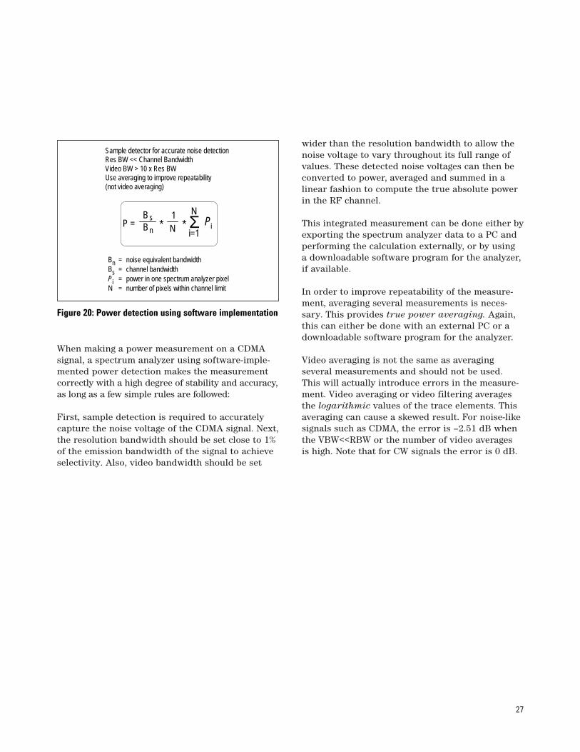
When making a power measurement on a CDMAsignal, a spectrum analyzer using software-imple-mented power detection makes the measurementcorrectly with a high degree of stability and accuracy,as long as a few simple rules are followed:
First, sample detection is required to accuratelycapture the noise voltage of the CDMA signal. Next,the resolution bandwidth should be set close to 1%of the emission bandwidth of the signal to achieveselectivity. Also, video bandwidth should be set
wider than the resolution bandwidth to allow thenoise voltage to vary throughout its full range ofvalues. These detected noise voltages can then beconverted to power, averaged and summed in a linear fashion to compute the true absolute powerin the RF channel.
This integrated measurement can be done either byexporting the spectrum analyzer data to a PC andperforming the calculation externally, or by using a downloadable software program for the analyzer,if available.
In order to improve repeatability of the measure-ment, averaging several measurements is neces-sary. This provides true power averaging. Again,this can either be done with an external PC or adownloadable software program for the analyzer.
Video averaging is not the same as averaging several measurements and should not be used.This will actually introduce errors in the measure-ment. Video averaging or video filtering averagesthe logarithmic values of the trace elements. Thisaveraging can cause a skewed result. For noise-likesignals such as CDMA, the error is –2.51 dB whenthe VBW<<RBW or the number of video averages is high. Note that for CW signals the error is 0 dB.
Figure 20: Power detection using software implementation
Sample detector for accurate noise detectionRes BW << Channel BandwidthVideo BW > 10 x Res BWUse averaging to improve repeatability(not video averaging)
N *i=1ΣN
iPB n
sB 1P =
Bn = noise equivalent bandwidthBs = channel bandwidthPi = power in one spectrum analyzer pixelN = number of pixels within channel limit
*
28
The 85725C CDMA personality software for theAgilent 8590 E-series spectrum analyzers automati-cally sets the instrument controls as described pre-viously and performs the necessary calculations.The results are reported in total power and inpower-spectral density in a 1 Hertz bandwidth.
A key advantage of the 85725C is its ability to aver-age several measurements, or perform true poweraveraging. CDMA signals are very noise-like andtherefore require averaging in order to improveaccuracy and repeatability.
This measurement can also be done using the built-in channel-power function on the 8590 E-seriesor 8560 E-series spectrum analyzers; however,these do not provide true power averaging, andwould therefore require exporting the data to a PC for improved repeatability.
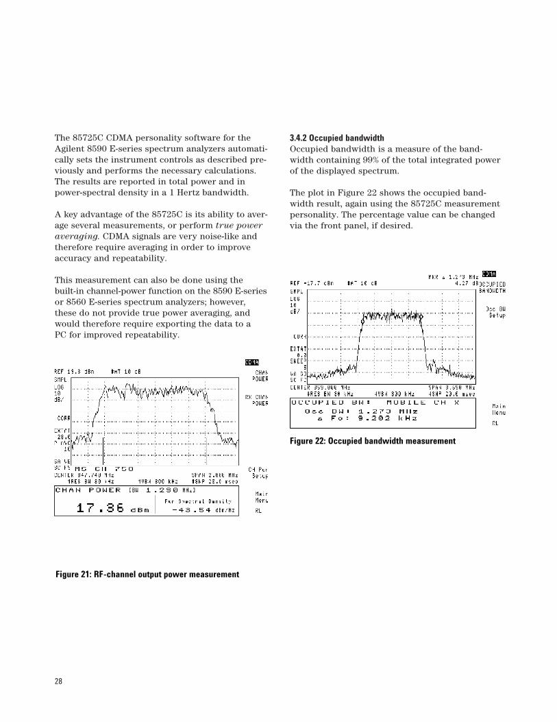
3.4.2 Occupied bandwidthOccupied bandwidth is a measure of the band-width containing 99% of the total integrated powerof the displayed spectrum.
The plot in Figure 22 shows the occupied band-width result, again using the 85725C measurementpersonality. The percentage value can be changedvia the front panel, if desired.
Figure 21: RF-channel output power measurement
Figure 22: Occupied bandwidth measurement
3.5 Out-of-channel measurementsThe last group of measurements covered are thosethat characterize the out-of-channel performanceof the amplifier. Linearity requirements are speci-fied by several figures of merit, including harmon-ics, adjacent-channel power, and spectral regrowth.These measurements tell us how much distortion iscaused by the non-linearities in the amplifier.
Amplifier linearity is critical to the performance ofCDMA systems. In these systems, the transmittedpower is very dynamic and can experience inputpower variations on the order of 20 dB. This drivesthe need for the amplifiers to operate linearly inthis range. Understanding the non-linear perform-ance is important since excessive distortion cancause interference in adjacent channels or otherfrequency bands.
Traditionally, characterizing the linearity perform-ance of a high-power amplifier required a two-toneintermodulation distortion (IMD) measurement,and was sufficient for analog FM systems such asAMPS cellular. While this is well understood anduses more common test equipment, tests such asadjacent-channel power and spectral regrowth arebecoming more accepted for measuring linearity ofpower amplifiers used in digital modulation systems.
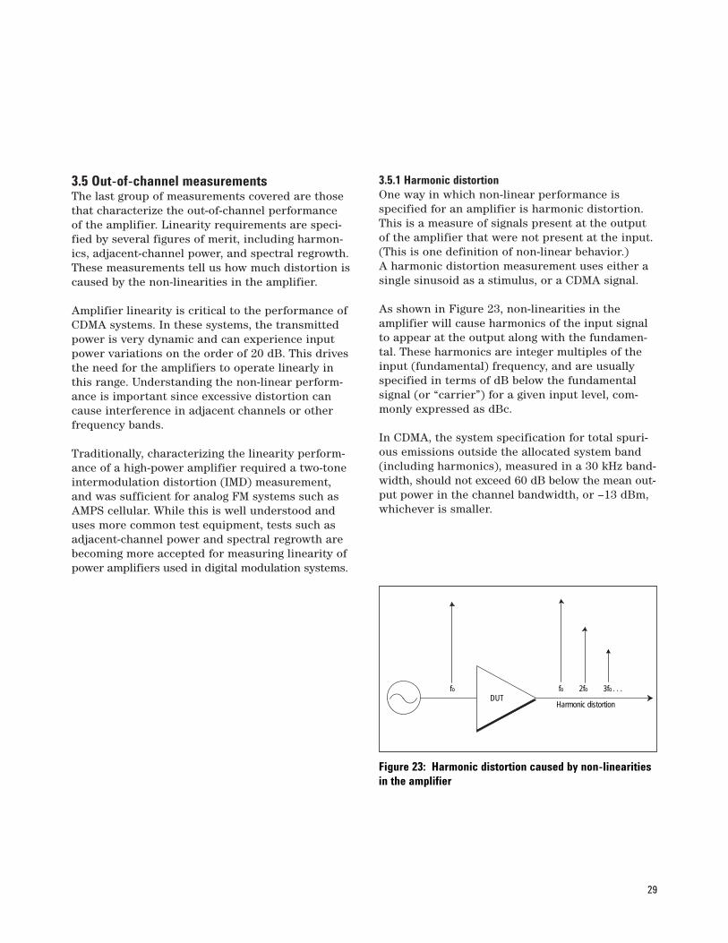
3.5.1 Harmonic distortionOne way in which non-linear performance is specified for an amplifier is harmonic distortion.This is a measure of signals present at the outputof the amplifier that were not present at the input.(This is one definition of non-linear behavior.) A harmonic distortion measurement uses either asingle sinusoid as a stimulus, or a CDMA signal.
As shown in Figure 23, non-linearities in theamplifier will cause harmonics of the input signalto appear at the output along with the fundamen-tal. These harmonics are integer multiples of theinput (fundamental) frequency, and are usuallyspecified in terms of dB below the fundamentalsignal (or “carrier”) for a given input level, com-monly expressed as dBc.
In CDMA, the system specification for total spuri-ous emissions outside the allocated system band(including harmonics), measured in a 30 kHz band-width, should not exceed 60 dB below the mean out-put power in the channel bandwidth, or –13 dBm,whichever is smaller.
. . .DUT
fo 3fo2fo fo
Harmonic distortion
29
Figure 23: Harmonic distortion caused by non-linearitiesin the amplifier
30
3.5.2 Adjacent channel power ratioAnother result of non-linear behavior in amplifiersis intermodulation distortion. Traditional inter-modulation testing uses two tones. This method,however, does not relate well quantitatively to theperformance in the final application for the com-plex base station amplifiers used in CDMA systems.
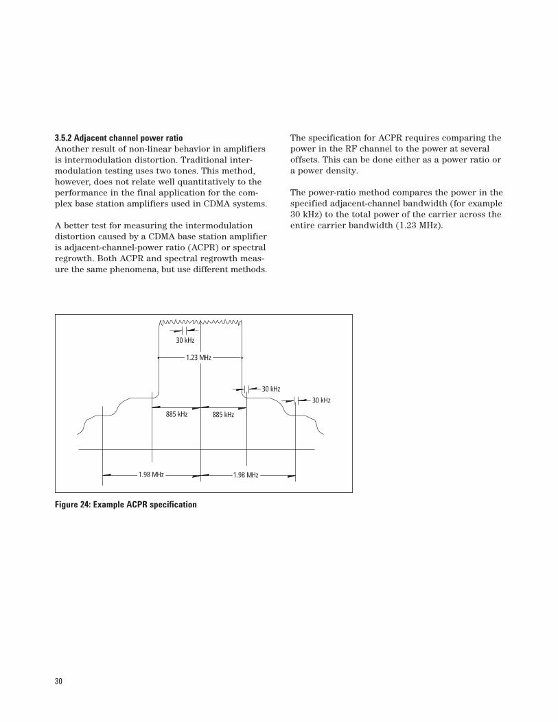
A better test for measuring the intermodulationdistortion caused by a CDMA base station amplifieris adjacent-channel-power ratio (ACPR) or spectralregrowth. Both ACPR and spectral regrowth meas-ure the same phenomena, but use different methods.
The specification for ACPR requires comparing thepower in the RF channel to the power at severaloffsets. This can be done either as a power ratio ora power density.
The power-ratio method compares the power in thespecified adjacent-channel bandwidth (for example30 kHz) to the total power of the carrier across theentire carrier bandwidth (1.23 MHz).
Figure 24: Example ACPR specification
30 kHz
30 kHz
30 kHz
885 kHz 885 kHz
1.98 MHz1.98 MHz
1.23 MHz
31
The power density method compares the powerdensity at the offset frequency, in a 30 kHz band-width, to the power within an average bandwidthof the same (30 kHz) width in the carrier-channelbandwidth. This is the Qualcomm Inc. recommendedmethod and can be calculated by normalizing the1.23 MHz channel-power result to a 30 kHz band-width (subtract 10log[1.23 MHz/30 kHz] = –16.13 dBfrom the result).
This test requires stimulating the amplifier with a CDMA signal. The measurement is then typicallymade on a spectrum analyzer.
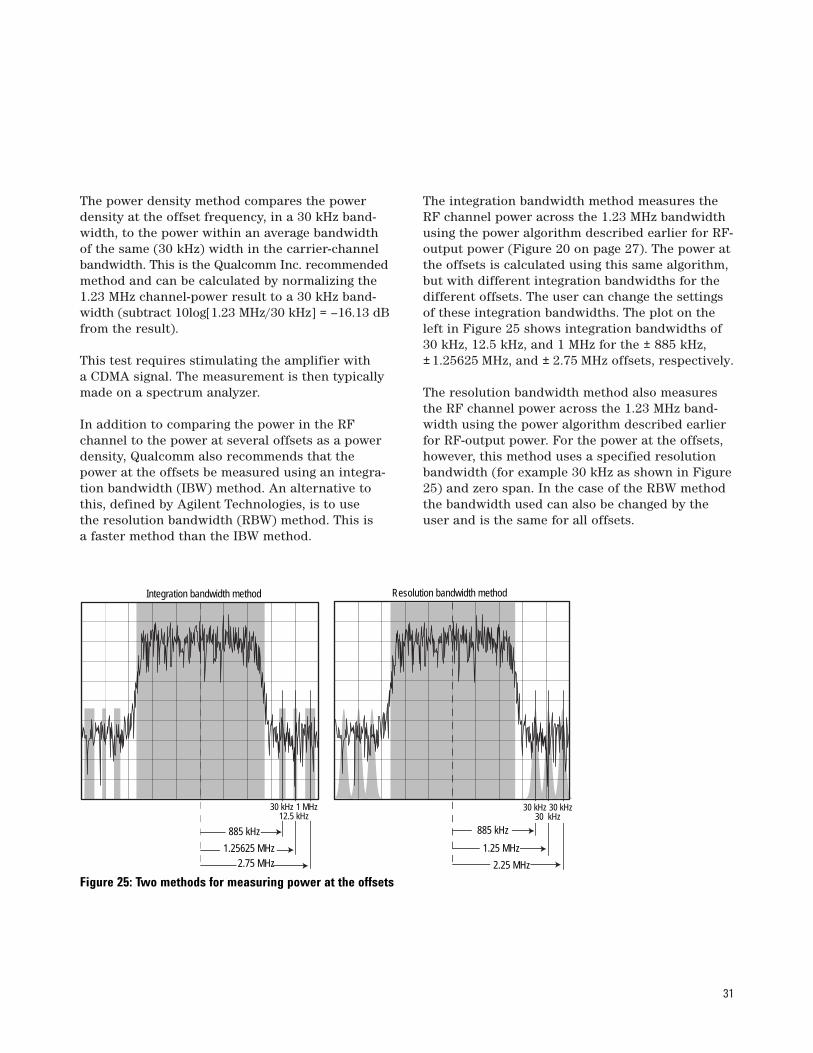
In addition to comparing the power in the RFchannel to the power at several offsets as a powerdensity, Qualcomm also recommends that thepower at the offsets be measured using an integra-tion bandwidth (IBW) method. An alternative tothis, defined by Agilent Technologies, is to use the resolution bandwidth (RBW) method. This is a faster method than the IBW method.
The integration bandwidth method measures theRF channel power across the 1.23 MHz bandwidthusing the power algorithm described earlier for RF-output power (Figure 20 on page 27). The power atthe offsets is calculated using this same algorithm,but with different integration bandwidths for thedifferent offsets. The user can change the settingsof these integration bandwidths. The plot on theleft in Figure 25 shows integration bandwidths of30 kHz, 12.5 kHz, and 1 MHz for the ± 885 kHz, ±1.25625 MHz, and ± 2.75 MHz offsets, respectively.
The resolution bandwidth method also measuresthe RF channel power across the 1.23 MHz band-width using the power algorithm described earlierfor RF-output power. For the power at the offsets,however, this method uses a specified resolutionbandwidth (for example 30 kHz as shown in Figure25) and zero span. In the case of the RBW methodthe bandwidth used can also be changed by theuser and is the same for all offsets.
30 kHz 1 MHz12.5 kHz
885 kHz
2.75 MHz1.25625 MHz
30 kHz 30 kHz30 kHz
885 kHz
2.25 MHz
1.25 MHz
Integration bandwidth method Resolution bandwidth method
Figure 25: Two methods for measuring power at the offsets
32
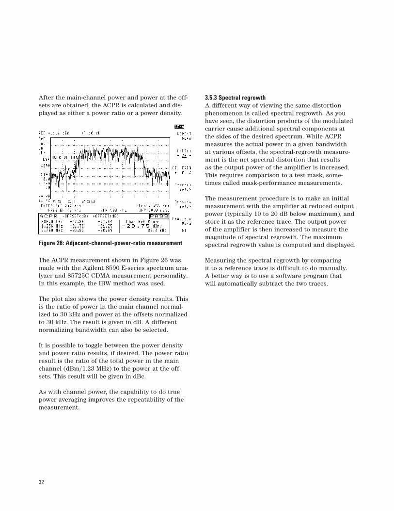
After the main-channel power and power at the off-sets are obtained, the ACPR is calculated and dis-played as either a power ratio or a power density.
The ACPR measurement shown in Figure 26 wasmade with the Agilent 8590 E-series spectrum ana-lyzer and 85725C CDMA measurement personality.In this example, the IBW method was used.
The plot also shows the power density results. Thisis the ratio of power in the main channel normal-ized to 30 kHz and power at the offsets normalizedto 30 kHz. The result is given in dB. A differentnormalizing bandwidth can also be selected.
It is possible to toggle between the power densityand power ratio results, if desired. The power ratioresult is the ratio of the total power in the mainchannel (dBm/1.23 MHz) to the power at the off-sets. This result will be given in dBc.
As with channel power, the capability to do truepower averaging improves the repeatability of themeasurement.
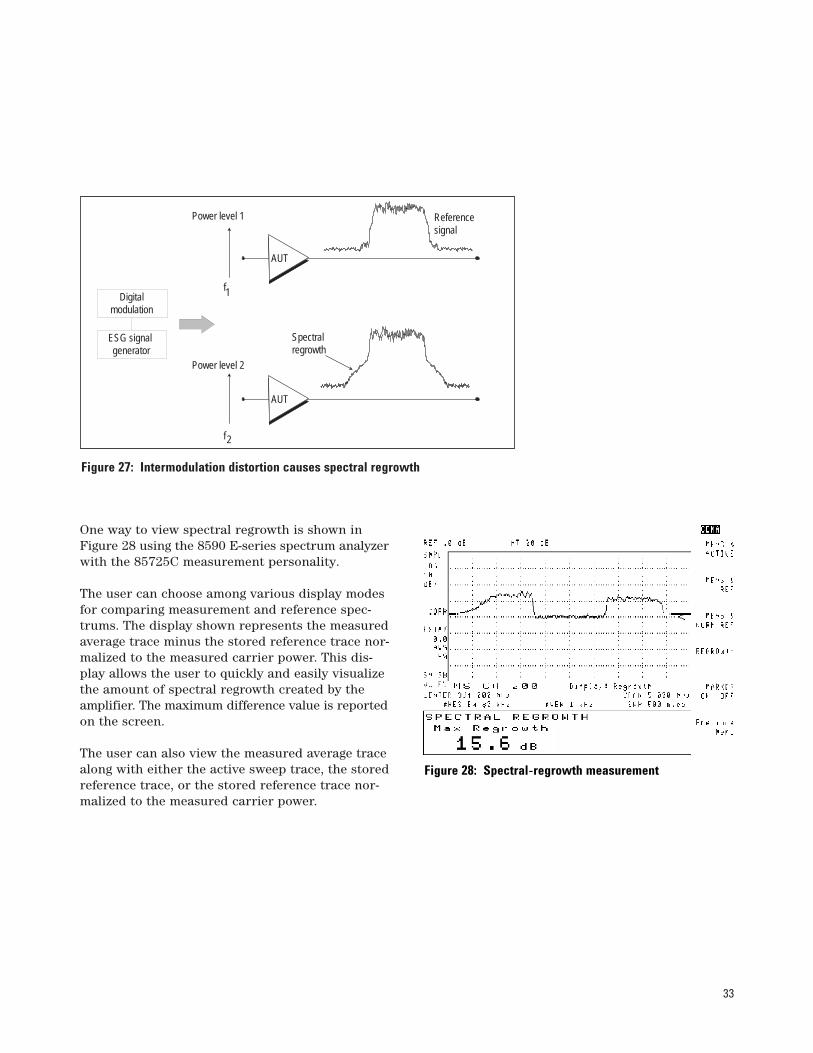
3.5.3 Spectral regrowthA different way of viewing the same distortionphenomenon is called spectral regrowth. As youhave seen, the distortion products of the modulatedcarrier cause additional spectral components atthe sides of the desired spectrum. While ACPRmeasures the actual power in a given bandwidth at various offsets, the spectral-regrowth measure-ment is the net spectral distortion that results as the output power of the amplifier is increased.This requires comparison to a test mask, some-times called mask-performance measurements.
The measurement procedure is to make an initialmeasurement with the amplifier at reduced outputpower (typically 10 to 20 dB below maximum), andstore it as the reference trace. The output power of the amplifier is then increased to measure themagnitude of spectral regrowth. The maximumspectral regrowth value is computed and displayed.
Measuring the spectral regrowth by comparing it to a reference trace is difficult to do manually. A better way is to use a software program that will automatically subtract the two traces.
Figure 26: Adjacent-channel-power-ratio measurement
33
One way to view spectral regrowth is shown inFigure 28 using the 8590 E-series spectrum analyzerwith the 85725C measurement personality.
The user can choose among various display modesfor comparing measurement and reference spec-trums. The display shown represents the measuredaverage trace minus the stored reference trace nor-malized to the measured carrier power. This dis-play allows the user to quickly and easily visualizethe amount of spectral regrowth created by theamplifier. The maximum difference value is reportedon the screen.
The user can also view the measured average tracealong with either the active sweep trace, the storedreference trace, or the stored reference trace nor-malized to the measured carrier power.
Figure 27: Intermodulation distortion causes spectral regrowth
f1Digitalmodulation
Power level 1
f2
Power level 2
Referencesignal
Spectralregrowth
AUT
AUT
ESG signal generator
Figure 28: Spectral-regrowth measurement
34
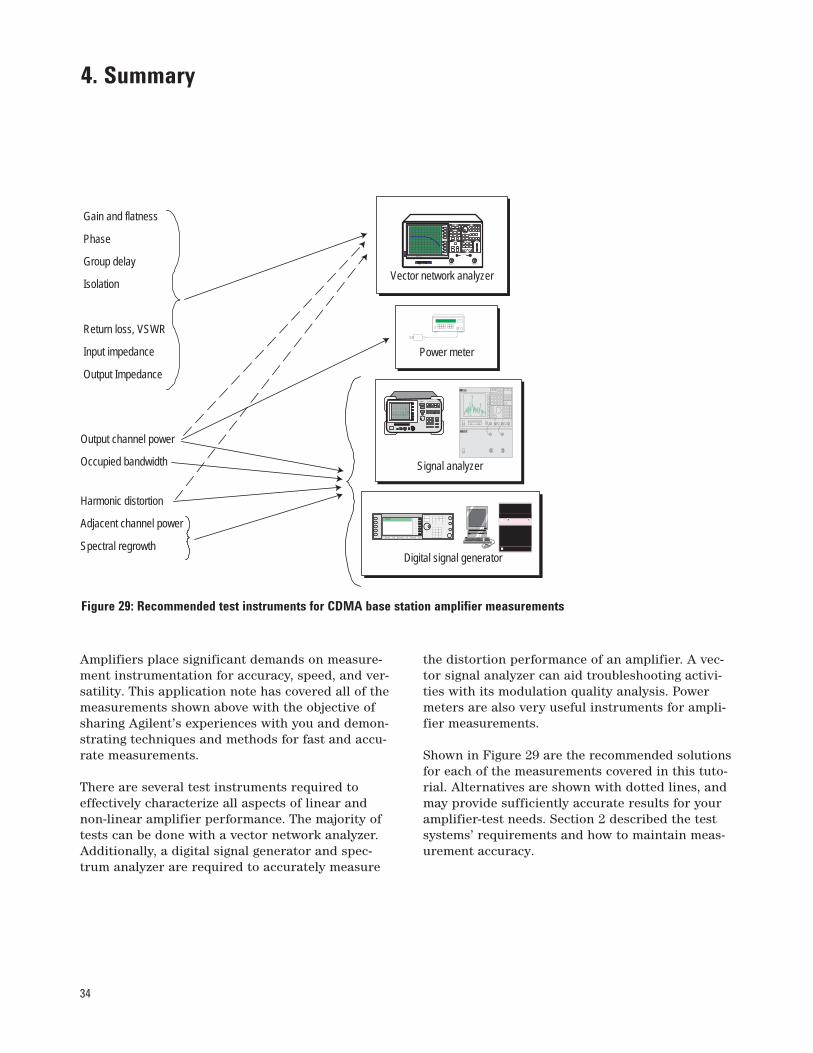
Amplifiers place significant demands on measure-ment instrumentation for accuracy, speed, and ver-satility. This application note has covered all of themeasurements shown above with the objective ofsharing Agilent’s experiences with you and demon-strating techniques and methods for fast and accu-rate measurements.
There are several test instruments required toeffectively characterize all aspects of linear andnon-linear amplifier performance. The majority oftests can be done with a vector network analyzer.Additionally, a digital signal generator and spec-trum analyzer are required to accurately measure
the distortion performance of an amplifier. A vec-tor signal analyzer can aid troubleshooting activi-ties with its modulation quality analysis. Powermeters are also very useful instruments for ampli-fier measurements.
Shown in Figure 29 are the recommended solutionsfor each of the measurements covered in this tuto-rial. Alternatives are shown with dotted lines, andmay provide sufficiently accurate results for youramplifier-test needs. Section 2 described the testsystems’ requirements and how to maintain meas-urement accuracy.
4. Summary
Figure 29: Recommended test instruments for CDMA base station amplifier measurements
Gain and flatness
Phase
Group delay
Isolation
Return loss, VSWR
Input impedance
Output Impedance
Output channel power
Occupied bandwidth
Harmonic distortion
Adjacent channel power
Spectral regrowth
Power meter
Signal analyzer
8563A SPECTRUM ANALYZER 9 kHz - 26.5 GHz
Vector network analyzer
H
ACTIVE CHANNEL
RESPONSE
STIMULUS
ENTRY
INSTRUMENT STATE R CHANNEL
R L T S
HP-IB STATUS
8753DNETWORK ANALYZER
30 KHz-3GHz
PROBE POWER FUSED
PORT 2PORT 1
Digital signal generator
1.90000
35
In conclusion, you have read about several impor-tant measurements that are made on a CDMA basestation amplifier. While not a complete or exhaus-tive list, these represent some of the more common,yet challenging, measurements.
Measurements particularly for design verificationinclude:
1) Pulsed bias and pulsed-RF techniques, whencombined together, create an environment thatis free from the adverse heating effects thatplague power amplifiers.
2) Load-pull techniques to optimize a power ampli-fier design for maximum power transfer.
Also for design verification and in a manufacturingenvironment, the following tests are important:
3) Network-analysis measurements which tell us a lot about an amplifier’s power efficiency andnetwork characteristics. Several network analyz-ers from Agilent Technologies are availabledepending on your needs.
4) In- and out-of-channel measurements for charac-terizing an amplifier’s output power and distor-tion performance. The ESG-D series signal generators provide an excellent CDMA stimulus.Multi-tone-testing capability is provided by theMulti-Format Communications Signal Simulator(MCSS). Measuring parameters such as outputpower, occupied bandwidth, and distortion iseasily accomplished with the 8590 E-series spec-trum analyzer with 85725C CDMA measurementpersonality. The 8560 E-series spectrum analyzerprovides higher performance, while the 89441Avector signal analyzer provides more sophisticatedsignal analysis and trouble-shooting capability.
1. Nick Kuhn, Bob Metreci, and Pete Thysell,“Proper Stimulus Ensures Accurate Tests of ACPfor the CDMA Forward Link,” article reprint5966-4786E.
2. Darin Phelps, “Measurement Solutions forTesting Base Station Amplifiers,” 1996 DeviceTest Seminar.
3. Using a Network Analyzer to Characterize High-Power Components, Agilent ApplicationNote 1287-6 (5966-3319E)
4. Digital Modulation in CommunicationsSystems—An Introduction, Agilent ApplicationNote 1298 (5965-7160E)
5. Spectrum Analysis, Agilent Application Note150 (5952-0292)
6. Understanding the Fundamental Principles ofVector Network Analysis, Agilent ApplicationNote 1287-1 (5965-7707)
7. Exploring the Architectures of NetworkAnalyzers, Agilent Application Note 1287-2(5965-7708E)
8. Applying Error Correction to Network AnalyzerMeasurements, Agilent Application Note 1287-3(5965-7709E)
9. Network Analyzer Measurments: Filter andAmplifier Examples, Agilent Application Note1287-4 (5965-7710E)
5. References
By internet, phone, or fax, get assistance with all your test and measurement needs.
Online Assistancewww.agilent.com/find/assistPhone or FaxUnited States:(tel) 1 800 452 4844
Canada:(tel) 1 877 894 4414(fax) (905) 206 4120
Europe:(tel) (31 20) 547 2323(fax) (31 20) 547 2390
Japan:(tel) (81) 426 56 7832(fax) (81) 426 56 7840
Latin America:(tel) (305) 269 7500(fax) (305) 269 7599
Australia:(tel) 1 800 629 485 (fax) (61 3) 9272 0749
New Zealand:(tel) 0 800 738 378 (fax) (64 4) 495 8950
Asia Pacific:(tel) (852) 3197 7777(fax) (852) 2506 9284
Product specifications and descriptions in this document subject to change without notice.
Copyright © 1998, 2000 Agilent TechnologiesPrinted in U.S.A. 5/005967-5486E