AFullyMicromachinedW-BandCoplanarWaveguide to ...users.ece.gatech.edu/etentze/IMS07_Yuan.pdf ·...
4
1 A Fully Micromachined W-Band Coplanar Waveguide to Rectangular Waveguide Transition Yuan Li, Bo Pan, Manos. M.Tentzeris and John Papapolymerou GEDC, School of Electrical & Computer Engineering, Georgia Institute of Technology, Atlanta, GA 30332 Abstract- A novel fully micromachined coplanar waveguide (CPW) to rectangular waveguide transition is presented in this paper. A metalized probe is adopted to couple the signal from the CPW to the rectangular waveguide through an aperture located at the center of the bottom broad wall of the rectangular waveguide. The transition was optimized using HFSS 10 over the whole W-band. In the proposed transition, the CPW and the rectangular waveguide are patterned and integrated on the same side of the substrate, while the coupling probe is patterned on the substrate instead of being fabricated separately. These changes make the transition more suitable for RF packaged circuits and easily extendable to THz applications. The measured average insertion loss of the back-to-back structure is 2.25dB and the return loss is better than 11 dB over the whole W-band. Index Terms- Micromachining, rectangular waveguide, Coplanar waveguide, Transition, Deep reactive ion etching, W-band I. INTRODUCTION Fueled by the demand of compact monolithic microwave integrated circuits (MMICs) for telecommunication and space applications, significant amount of research has been performed on coplanar waveguide (CPW) based topologies due to CPW's several advantages over other competing transmission lines [1,2]: The grounds and the signal are on the same side of the substrate eliminating the need for via-holes or wraparound process [3,4]. Also, the characteristic impedance is determined by the ratio of the width of center strip conductor to the distance between the two semi-infinite ground planes [5] enabling compact designs, something demonstrated by the numerous CPW-based microwave probes commonly used for the characterization of microwave integrated circuits. Rectangular waveguides, on the other hand, have the advantages of low loss and high power handling capacity. However, the traditional rectangular waveguides at low frequencies are bulky making almost impossible their integration into system-on-chip geometries. Nevertheless, the size of rectangular waveguides shrinks dramatically at or above the mm-wave frequency range or even in Terahertz frequencies [6]-[8]. At the same time, the losses of other transmission lines, such as microstrips, keep increasing when the frequency goes up. Various transitions from CPW to rectangular waveguide have been proposed in the past, in order to combine their respective advantages. Either a ridge and a non-radiating slot, located at opposite sides of the broad wall of the rectangular waveguide [9] or a ridge and a trough [10], are introduced to convert the waveguide TE1o mode into the CPW field. In [ 1 1], two transitions, the post coupler and the slot coupler, are demonstrated and in [12] fully micromachined transitions are shown using the probes on finite-ground coplanar line. This paper presents a novel fully micromachined CPW to rectangular waveguide transition. Compared to [9, 10], the proposed transition has the advantage of easier mass production by using the silicon micromachining technique. The CPW and the rectangular waveguide are patterned and integrated on the same side of the substrate in this paper instead of the both sides of the substrate [11]. Plus, the coupling probe is patterned on the substrate instead of being fabricated separately [12]. The proposed transition doesn't need the probe assembly like [12]. These changes make the transition more suitable for RF packaged circuits and easily extendable to THz applications. II. TRANSITION DESIGN AND SIMULATION . %Mo. * R . a.... Fig. 1. The schematic diagram of the transition. 1-4244-0688-9/07/$20.00 C 2007 IEEE 1031
Transcript of AFullyMicromachinedW-BandCoplanarWaveguide to ...users.ece.gatech.edu/etentze/IMS07_Yuan.pdf ·...

1
A Fully Micromachined W-Band Coplanar Waveguide toRectangular Waveguide Transition
Yuan Li, Bo Pan, Manos. M.Tentzeris and John Papapolymerou
GEDC, School of Electrical & Computer Engineering, Georgia Institute of Technology, Atlanta, GA 30332
Abstract- A novel fully micromachined coplanar waveguide(CPW) to rectangular waveguide transition is presented in thispaper. A metalized probe is adopted to couple the signal from theCPW to the rectangular waveguide through an aperture locatedat the center of the bottom broad wall of the rectangularwaveguide. The transition was optimized using HFSS 10 over thewhole W-band. In the proposed transition, the CPW and therectangular waveguide are patterned and integrated on the sameside of the substrate, while the coupling probe is patterned on thesubstrate instead of being fabricated separately. These changesmake the transition more suitable for RF packaged circuits andeasily extendable to THz applications. The measured averageinsertion loss of the back-to-back structure is 2.25dB and thereturn loss is better than 11 dB over the whole W-band.
Index Terms- Micromachining, rectangular waveguide,Coplanar waveguide, Transition, Deep reactive ion etching,W-band
I. INTRODUCTION
Fueled by the demand of compact monolithic microwaveintegrated circuits (MMICs) for telecommunication andspace applications, significant amount ofresearch has been
performed on coplanar waveguide (CPW) based topologiesdue to CPW's several advantages over other competingtransmission lines [1,2]: The grounds and the signal are on thesame side of the substrate eliminating the need for via-holes orwraparound process [3,4]. Also, the characteristic impedance isdetermined by the ratio ofthe width of center strip conductor tothe distance between the two semi-infinite ground planes [5]enabling compact designs, something demonstrated by thenumerous CPW-based microwave probes commonly used forthe characterization ofmicrowave integrated circuits.
Rectangular waveguides, on the other hand, have theadvantages of low loss and high power handling capacity.However, the traditional rectangular waveguides at lowfrequencies are bulky making almost impossible theirintegration into system-on-chip geometries. Nevertheless, thesize ofrectangular waveguides shrinks dramatically at or abovethe mm-wave frequency range or even in Terahertz frequencies[6]-[8]. At the same time, the losses of other transmission lines,
such as microstrips, keep increasing when the frequency goesup.
Various transitions from CPW to rectangular waveguidehave been proposed in the past, in order to combine theirrespective advantages. Either a ridge and a non-radiating slot,located at opposite sides of the broad wall of the rectangularwaveguide [9] or a ridge and a trough [10], are introduced toconvert the waveguide TE1o mode into the CPW field. In [1 1],two transitions, the post coupler and the slot coupler, aredemonstrated and in [12] fully micromachined transitions areshown using the probes on finite-ground coplanar line.
This paper presents a novel fully micromachined CPW torectangular waveguide transition. Compared to [9, 10], theproposed transition has the advantage of easier mass productionby using the silicon micromachining technique. The CPW andthe rectangular waveguide are patterned and integrated on thesame side ofthe substrate in this paper instead ofthe both sidesof the substrate [11]. Plus, the coupling probe is patterned onthe substrate instead of being fabricated separately [12]. Theproposed transition doesn't need the probe assembly like [12].These changes make the transition more suitable for RFpackaged circuits and easily extendable to THz applications.
II. TRANSITION DESIGN AND SIMULATION
.
%Mo. *R .a....
Fig. 1. The schematic diagram of the transition.
1-4244-0688-9/07/$20.00 C 2007 IEEE 1031

2
This on-wafer CPW to rectangular waveguide transition iscomposed of two parts: a CPW to vertical probe part and aprobe to waveguide part, as shown in Fig. 1. The CPW line ispatterned on the top of the quartz substrate and is firstterminated into a vertical probe [13], which is then inserted intothe waveguide through its bottom broad wall. Themicromachined waveguide is mounted on top of the quartzsubstrate (diel.constant 3.78), with a rectangular slit etched tofeed the CPW in. The whole rectangular waveguide is made byfour silicon layers, which are stacked and aligned together [14].
Contrary to previous approaches, in this paper the CPW lineis fabricated on the top of the quartz glass with 1.5mmthickness. The vertical coupling probe is patterned on thequartz substrate. The impedance ofthe coaxial structure formedby the probe and the metalized silicon hole is provided by:
Table 1. The dimensions ofthe transition
V
v)04a)
LL(1)Zc= I UL 1/J R2C 2rT£)' RI
where, is the permeability of the vacuum, c'is the real
permittivity and R2 and RI are the radii ofthe aperture and theprobe, respectively. The impedance of the coaxial structure isselected to match the impedance of the CPW. However, theparasitics caused by the discontinuity of circular aperture andthe circular tapering ofthe CPW ground around probe is one ofthe reasons that cause the mismatching in the measurement ofreturn loss.
The standard WR-10 waveguide dimensions (2.54mm x1.27mm) are utilized for the rectangular waveguide. The siliconlayer on the bottom is patterned on a 300um thick wafer. TheCPW line is fabricated on the top of a 1.5mm thick quartzsubstrate. The CPW beyond the probe is terminated in ashort-stub for achieving a good impedance matching. Theprobe is located in the center of the broad wall. The design oftransition from probe to waveguide is based on matching thecoaxial structure with probe to waveguide. The distance fromprobe to backshort (L in Fig.2), the height of the probe and theradius of the probe are critical in the matching. Finally, thetransition is optimized using the full-wave simulator, HFSS,leading to the dimensions, shown in Fig. 2 and listed in Table 1,while the optimized insertion loss and return loss of thetransition are shown in Fig. 3.
Dimensions Value(um)HI 850H2 150RI 115R2 400W 40S 240L 885
$21
-215 -- -- -r r, l ,8311
I5 ------- --------------------I-------- I--- ---g--- ----r----
435 --- 0---------------- ---------- --------- ---------- ---------- -------- -
5S 80 85 90 95 100 105 1 1Frequency (GHz)
Fig. 3.The simulated insertion loss and return loss.
10
To facilitate the measurement, the transition structure isfabricated in a back-to-back configuration that is shown in Fig.4. The optimized simulation of the back-to-back transition isprovided in Fig. 5. The simulated insertion loss of theback-to-back structure is between 0.87 dB and 2.68 dB overW-band (75-1 1OGHz).
Fig. 4. The back-to-back structure.
-10-
15-
0) -20Eco 25~
-7
Fig. 5.The simulated insertion loss and return loss ofthe back-to-back structure.
Fig. 2. The CPW and the coupling probe (The transition is shown in half fromthe center ofthe broad wall due to its symmetry, the metalized silicon sidewallswith thickness T are not shown).
1032

3
D. Fabricationflow ofthefeeding CPWand the probe
III. FABRICATION
A. Fixture
A fixture, shown in Fig. 6(a), was designed to facilitate thealignment. The alignment pins were applied on the base of thefixture and provided the reference to align the silicon parts andhelped to snap them together.
B. Stacked substratesFour silicon layers were fabricated using the deep reactive
ion etching (DRIE) technique. The bottom layer was made by a300um thick silicon wafer. The aperture was patterned on thiswafer. The two middle layers were fabricated using the 525umthick wafers. The top layer was etched only 220um deep withthe pattern of the rectangular waveguide and released from theback. Finally, the four silicon layers formed a rectangularwaveguide with a 1.27mm height. The metalized probe wasfabricated on the 1.5mm quartz substrate as well as the CPWline. A picture of the fixture and the stacked samples wereshown in Fig. 6.
The Ti/Cu/Ti layer was sputtered and patterned to open thewindow for the SU-8 patterning from the backside of thetransparent quartz wafer. This improves the SU-8 adhesion tothe quartz. An 800 ptm negative photo-definable epoxy SU-82035 was dispensed uniformly on the top of the glass. It waspatterned under UV to define the mold of the vertical probe.Another Ti/Cu/Ti was sputtered as the seed layer to cover theprobes, as well as the substrate in a conformal manner. Then,the negative photo-resist NR9-8000 was coated and patternedin a non-contact way to cover the CPW slot region, preventingthe metal coverage on the slot in the following electroplatingstep. 6ptm copper and 2pm gold were electroplated to cover thesidewall of the probe, as well as the exposed ground feedingstructures. As the final step, the photo-resist NR9-8000, as wellas the seed layer were removed one by one to release thestructure. The fabrication flow is shown in Fig. 7-2. Fig.8 givesthe SEM picture of the probe and the aperture on the 300umthick wafer.
Ti/Cu/Ti
SU-8
(a)Glai
SU-8 probe UVA"k Ti/CulTi
UV
NR9-8000l-
ta) V u)Fig. 6. (a) The fixture, quartz substrate and the silicon layers. (b) The wholetransition with fixture.
CPW slots C\\
| (d)
C. Fabricationflow ofthe Silicon wafer
The first step of the silicon substrate preparation was wafercleaning. Then, photoresist(PR) SRP220 was spun andpatterned on the topside of the silicon wafer. The patternedwafer was baked at 115 degrees for 5 minutes, before the STSICP was applied to etch the topside to the desired depth. Aclean process was utilized to clean the remaining PR from thetopside etching. Then, the Uniaxis PECVD was used to deposita thin silicon dioxide layer to protect the patterned topside.Once the silicon dioxide was deposited, the wafer was flippedand patterned using the PR on the backside. Then, the samplewas released by using the backside etching. Finally, BOE wasapplied to remove the silicon dioxide layer. The silicon sampleswere metallized using DC-Sputter with Ti/Cu/Au. Thefabrication flow was shown in Fig. 7-1.
(e)Fig. 7-1 Fig.7-2
Fig. 7. (1) The fabrication flow of silicon rectangular waveguide. (2). Thefabrication flow ofCPW and Probe
Fig. 8. (a) The probe and CPW. (b) The aperture on the 300um thick wafer.
1033
4
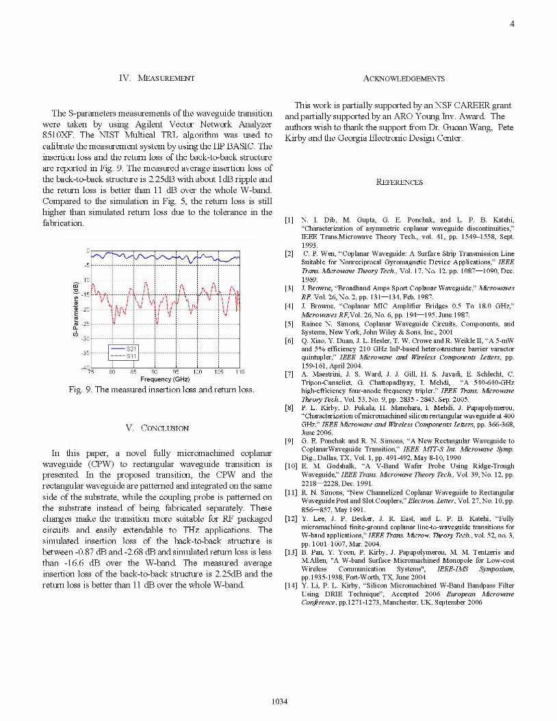
IV. MEASUREMENT
The S-parameters measurements of the waveguide transitionwere taken by using Agilent Vector Network Analyzer851OXF. The NIST Multical TRL algorithm was used tocalibrate the measurement system by using the UP BASIC. Theinsertion loss and the return loss of the back-to-back structureare reported in Fig. 9. The measured average insertion loss ofthe back-to-back structure is 2.25dB with about 1dB ripple andthe return loss is better than 11 dB over the whole W-band.Compared to the simulation in Fig. 5, the return loss is stillhigher than simulated return loss due to the tolerance in thefabrication.
10
EY5 -25 --- -- -- -- -n- -- -- --- .- -- -- - - - - - -- - - - -- - -- -- -- - -- - -- -- -- -- r- -- -- - ---
C;)
S21350 -- -- - - - - -- ---------- -- -- - -- --r -- -- - -- --n - -- -- - -- --I- -- -- - -- --r - -- - -- ---
I---- S1l
_4nj75 80 85 90 95 100 105 110
Frequency (GHz)Fig. 9. The measured insertion loss and return loss.
V. CONCLUSION
In this paper, a novel fully micromachined coplanarwaveguide (CPW) to rectangular waveguide transition ispresented. In the proposed transition, the CPW and therectangular waveguide are patterned and integrated on the sameside of the substrate, while the coupling probe is patterned onthe substrate instead of being fabricated separately. Thesechanges make the transition more suitable for RF packagedcircuits and easily extendable to THz applications. Thesimulated insertion loss of the back-to-back structure isbetween -0.87 dB and -2.68 dB and simulated return loss is lessthan -16.6 dB over the W-band. The measured averageinsertion loss of the back-to-back structure is 2.25dB and thereturn loss is better than 11 dB over the whole W-band.
ACKNOWLEDGEMENTS
This work is partially supported by an NSF CAREER grantand partially supported by an ARO Young Inv. Award. Theauthors wish to thank the support from Dr. Guoan Wang, PeteKirby and the Georgia Electronic Design Center.
REFERENCES
[1] N. I. Dib, M. Gupta, G. E. Ponchak, and L. P. B. Katehi,"Characterization of asymmetric coplanar waveguide discontinuities,"IEEE Trans.Microwave Theory Tech., vol. 41, pp. 1549-1558, Sept.1993.
[2] C. P. Wen, "Coplanar Waveguide: A Surface Strip Transmission LineSuitable for Nonreciprocal Gyromagnetic Device Applications," IEEETrans. Microwave Theory Tech., Vol. 17, No. 12, pp. 1087 1090, Dec.1969.
[3] J. Browne, "Broadband Amps Sport Coplanar Waveguide," MicrowavesRF, Vol. 26, No. 2, pp. 131 134, Feb. 1987.
[4] J. Browne, "Coplanar MIC Amplifier Bridges 0.5 To 18.0 GHz,"Microwaves RF,Vol. 26, No. 6, pp. 194 195, June 1987.
[5] Rainee N. Simons, Coplanar Waveguide Circuits, Components, andSystems, New York, John Wiley & Sons, Inc., 2001
[6] Q. Xiao, Y. Duan, J. L. Hesler, T. W. Crowe and R. Weikle II, "A 5-mWand 5% efficiency 210 GHz InP-based heterostructure barrier varactorquintupler," IEEE Microwave and Wireless Components Letters, pp.159-161, April 2004.
[7] A. Maestrini, J. S. Ward, J. J. Gill, H. S. Javadi, E. Schlecht, C.Tripon-Canseliet, G. Chattopadhyay, I. Mehdi, "A 540-640-GHzhigh-efficiency four-anode frequency tripler," IEEE Trans. MicrowaveTheory Tech., Vol. 53, No. 9, pp. 2835 - 2843, Sep. 2005.
[8] P. L. Kirby, D. Pukala, H. Manohara, I. Mehdi, J. Papapolymerou,"Characterization ofmicromachined silicon rectangular waveguide at 400GHz," IEEE Microwave and Wireless Components Letters, pp. 366-368,June 2006.
[9] G. E. Ponchak and R. N. Simons, "A New Rectangular Waveguide toCoplanarWaveguide Transition," IEEE MTT-S Int. Microwave Symp.Dig., Dallas, TX, Vol. 1, pp. 491-492, May 8-10, 1990
[10] E. M. Godshalk, "A V-Band Wafer Probe Using Ridge-TroughWaveguide," IEEE Trans. Microwave Theory Tech., Vol. 39, No. 12, pp.2218 2228, Dec. 1991.
[11] R. N. Simons, "New Channelized Coplanar Waveguide to RectangularWaveguide Post and Slot Couplers," Electron. Letter, Vol. 27, No. 10, pp.856 857, May 1991.
[12] Y. Lee, J. P. Becker, J. R. East, and L. P. B. Katehi, "Fullymicromachined finite-ground coplanar line-to-waveguide transitions forW-band applications," IEEE Trans. Microw. Theory Tech., vol. 52, no. 3,pp. 1001-1007, Mar. 2004.
[13] B. Pan, Y. Yoon, P. Kirby, J. Papapolymerou, M. M. Tentzeris andM.Allen, "A W-band Surface Micromachined Monopole for Low-costWireless Communication Systems", IEEE-IMS Symposium,pp.1935-1938, Fort-Worth, TX, June 2004
[14] Y. Li, P. L. Kirby, "Silicon Micromachined W-Band Bandpass FilterUsing DRIE Technique", Accepted 2006 European MicrowaveConference, pp. 1271-1273, Manchester, UK, September 2006
1034