AFRL-RQ-WP-TR-2014-0212 - Defense Technical Information · PDF fileAFRL-RQ-WP-TR-2014-0212 ....
13
AFRL-RQ-WP-TR-2014-0212 A BROADBAND HIGH-GAIN BI-LAYER LOG-PERIODIC DIPOLE ARRAY (LPDA) FOR ULTRA HIGH FREQUENCY (UHF) CONFORMAL LOAD BEARING ANTENNA STRUCTURES (CLAS) APPLICATIONS Nicholas A. Bishop and Mohammod Ali University of South Carolina Jason Miller, David L. Zeppettella, William Baron, and James Tuss Structures Technology Branch Aerospace Vehicles Division AUGUST 2014 Interim Report Approved for public release; distribution unlimited. See additional restrictions described on inside pages STINFO COPY AIR FORCE RESEARCH LABORATORY AEROSPACE SYSTEMS DIRECTORATE WRIGHT-PATTERSON AIR FORCE BASE, OH 45433-7541 AIR FORCE MATERIEL COMMAND UNITED STATES AIR FORCE
Transcript of AFRL-RQ-WP-TR-2014-0212 - Defense Technical Information · PDF fileAFRL-RQ-WP-TR-2014-0212 ....

AFRL-RQ-WP-TR-2014-0212
A BROADBAND HIGH-GAIN BI-LAYER LOG-PERIODIC DIPOLE ARRAY (LPDA) FOR ULTRA HIGH FREQUENCY (UHF) CONFORMAL LOAD BEARING ANTENNA STRUCTURES (CLAS) APPLICATIONS Nicholas A. Bishop and Mohammod Ali University of South Carolina Jason Miller, David L. Zeppettella, William Baron, and James Tuss Structures Technology Branch Aerospace Vehicles Division AUGUST 2014 Interim Report
Approved for public release; distribution unlimited.
See additional restrictions described on inside pages
STINFO COPY
AIR FORCE RESEARCH LABORATORY AEROSPACE SYSTEMS DIRECTORATE
WRIGHT-PATTERSON AIR FORCE BASE, OH 45433-7541 AIR FORCE MATERIEL COMMAND
UNITED STATES AIR FORCE

NOTICE AND SIGNATURE PAGE
Using Government drawings, specifications, or other data included in this document for any purpose other than Government procurement does not in any way obligate the U.S. Government. The fact that the Government formulated or supplied the drawings, specifications, or other data does not license the holder or any other person or corporation; or convey any rights or permission to manufacture, use, or sell any patented invention that may relate to them. This report was cleared for public release by the USAF 88th Air Base Wing (88 ABW) Public Affairs Office (PAO) and is available to the general public, including foreign nationals. Copies may be obtained from the Defense Technical Information Center (DTIC) (http://www.dtic.mil). AFRL-RQ-WP-TR-2014-0212 HAS BEEN REVIEWED AND IS APPROVED FOR PUBLICATION IN ACCORDANCE WITH ASSIGNED DISTRIBUTION STATEMENT. *//Signature// //Signature// DAVID L. ZEPPETTELLA MICHAEL R. WIPPERMAN, Acting Chief Work Unit Manager Structures Technology Branch Structures Technology Branch Aerospace Vehicles Division Aerospace Vehicles Division //Signature// FRANK C. WITZEMAN Chief Aerospace Vehicles Division Aerospace Systems Directorate This report is published in the interest of scientific and technical information exchange, and its publication does not constitute the Government’s approval or disapproval of its ideas or findings. *Disseminated copies will show “//Signature//” stamped or typed above the signature blocks.

REPORT DOCUMENTATION PAGE Form Approved OMB No. 0704-0188
The public reporting burden for this collection of information is estimated to average 1 hour per response, including the time for reviewing instructions, searching existing data sources, gathering and maintaining the data needed, and completing and reviewing the collection of information. Send comments regarding this burden estimate or any other aspect of this collection of information, including suggestions for reducing this burden, to Department of Defense, Washington Headquarters Services, Directorate for Information Operations and Reports (0704-0188), 1215 Jefferson Davis Highway, Suite 1204, Arlington, VA 22202-4302. Respondents should be aware that notwithstanding any other provision of law, no person shall be subject to any penalty for failing to comply with a collection of information if it does not display a currently valid OMB control number. PLEASE DO NOT RETURN YOUR FORM TO THE ABOVE ADDRESS.
1. REPORT DATE (DD-MM-YY) 2. REPORT TYPE 3. DATES COVERED (From - To) August 2014 Interim 01 October 2012 – 26 August 2014
4. TITLE AND SUBTITLE
A BROADBAND HIGH-GAIN BI-LAYER LOG-PERIODIC DIPOLE ARRAY (LPDA) FOR ULTRA HIGH FREQUENCY (UHF) CONFORMAL LOAD BEARING ANTENNA STRUCTURES (CLAS) APPLICATIONS
5a. CONTRACT NUMBER In-house
5b. GRANT NUMBER
5c. PROGRAM ELEMENT NUMBER 62201F
6. AUTHOR(S)
Nicholas A. Bishop and Mohammod Ali (University of South Carolina) Jason Miller, David L. Zeppettella, William Baron, and James Tuss (AFRL/RQVS)
5d. PROJECT NUMBER 2401
5e. TASK NUMBER 5f. WORK UNIT NUMBER
Q07D 7. PERFORMING ORGANIZATION NAME(S) AND ADDRESS(ES) 8. PERFORMING ORGANIZATION
REPORT NUMBER AFRL-RQ-WP-TR-2014-0212
University of South Carolina Department of Electrical Engineering Columbia, SC 29208
Structures Technology Branch (AFRL/RQVS) Aerospace Vehicles Division Air Force Research Laboratory, Aerospace Systems Directorate Wright-Patterson Air Force Base, OH 45433-7541 Air Force Materiel Command, United States Air Force
9. SPONSORING/MONITORING AGENCY NAME(S) AND ADDRESS(ES) 10. SPONSORING/MONITORING Air Force Research Laboratory Aerospace Systems Directorate Wright-Patterson Air Force Base, OH 45433-7541 Air Force Materiel Command United States Air Force
AGENCY ACRONYM(S) AFRL/RQVS
11. SPONSORING/MONITORING AGENCY REPORT NUMBER(S) AFRL-RQ-WP-TR-2014-0212
12. DISTRIBUTION/AVAILABILITY STATEMENT Approved for public release; distribution unlimited.
13. SUPPLEMENTARY NOTES PA Case Number: 88ABW-2014-3668; Clearance Date: 08 Aug 2014.
14. ABSTRACT A broadband high-gain bi-layer log-periodic dipole array (LPDA) is introduced for conformal load bearing antenna structures (CLAS) applications. Under the proposed scheme the two layers of the LPDA are printed on two separate thin dielectric substrates which are substantially separated from each other. A meander line geometry is adapted to achieve size reduction for the array. The fabricated and tested array easily exceeds more than an octave of gain, pattern, and VSWR bandwidth.
15. SUBJECT TERMS broadband antenna, array, log-periodic, LPDA, endfire, ultrawideband, UWB, CLAS
16. SECURITY CLASSIFICATION OF: 17. LIMITATION OF ABSTRACT:
SAR
18. NUMBER OF PAGES
16
19a. NAME OF RESPONSIBLE PERSON (Monitor) a. REPORT Unclassified
b. ABSTRACT Unclassified
c. THIS PAGE Unclassified
David L. Zeppettella 19b. TELEPHONE NUMBER (Include Area Code)
N/A
Standard Form 298 (Rev. 8-98) Prescribed by ANSI Std. Z39-18

1
Abstract— A broadband high-gain bi-layer Log-Periodic-
Dipole-Array (LPDA) is introduced for Conformal Load Bearing
Antenna Structures (CLAS) applications. Under the proposed
scheme the two layers of the LPDA are printed on two separate
thin dielectric substrates which are substantially separated from
each other. A meander line geometry is adapted to achieve size
reduction for the array. The fabricated and tested array easily
exceeds more than an octave of gain, pattern and VSWR
bandwidth.
Index Terms — Broadband antenna, array, log-periodic, LPDA,
endfire, ultrawideband, UWB, CLAS.
I. INTRODUCTION
he study of Log Periodic Dipole Antennas (LPDAs) dates
back many decades [1]-[27]. LPDAs have been studied
and designed for operation in free-space [1]-[4] as well as
in printed configurations [5]-[8]. The works in [7, 8] propose a
new technique to design and build stripline fed LPDAs in the
microwave frequency band. These designs consider low
dielectric constant materials and thin (few mm) printed
embodiments. A printed meander dipole LPDA was proposed
in [9] for operation from around 2-4.5 GHz. The peak array
gain achieved was 7.5 dBi. Approximately 12% size reduced
(Log Periodic Koch Dipole Arrays) LKPDAs were proposed
in [10]. These microstrip LKPDAs operate from 2-3.2 GHz.
An LPDA design for ultrawideband pulse radiation has
been proposed in [11]-[12]. More recently, a microstrip-fed
band notched UWB LPDA was proposed in [13] for operation
in the 4-10 GHz frequency range. The array peak gain was in
the vicinity of 5 dBi.
It is apparent that many design examples of microstrip or
stripline fed LPDAs exist for frequencies 1 GHz or higher.
Similarly relatively low-gain (4 dBi) broadband UHF LPDAs
also exist that consist of two very closely spaced
(approximately 1 mm) dipole layers fed using a coaxial line
[28].
This work was supported in part by the Air Force Research Laboratory (AFRL), Wright Patterson Air Force Base, Contract # 12-S2603-04-C01.
Cleared for Public Release - Case Number: .
Nicholas Bishop and M. Ali are with the Department of Electrical
Engineering, University of South Carolina, Columbia, SC 29208 USA (email.
[email protected]; [email protected]). Jason Miller, David Zeppettella, William Baron, and James Tuss are with the AFRL, Wright Patterson Air
Force Base, Ohio (email. [email protected],
[email protected], [email protected], [email protected]).
The focus of the present work is to introduce the design and
development concepts of a broadband UHF LPDA that allows
Conformal Load Bearing Antenna Structure (CLAS)
integration. The CLAS concept [29-32] pioneered for air
vehicle integration and application allows an antenna and its
surrounding structure to become one seamless entity. This
approach offers the optimum leveraging of materials and
structures and significantly reduces the weight and drag
associated with conventional antenna integration schemes.
The integration efficiency of CLAS enables an air vehicle to
host unconventionally large antenna leading to increased
antenna performance potential.
Fig. 1. Illustration showing the proposed CLAS LPDA in a structural
sandwich. Top picture - longer dipoles or low band. Bottom picture – shorter
dipoles or high band. Coax inner conductor shorted to feed tube using a
copper plate.
The target RF performance requirements are: greater than
an octave of gain, pattern, and VSWR bandwidths with a
starting frequency of 350 MHz. Greater than 7 dBi of peak
gain, large Forward to Backward ratio (F/B), and an endfire
beam are desired. The proposed CLAS integration
requirements are such that the antenna trace layers can be
disposed of on two separate surfaces that are separated from
each other by a substantial distance (1-2 inches). Further
A Broadband High-Gain Bi-Layer LPDA for UHF
Conformal Load Bearing Antenna Structures (CLAS)
Applications Nicholas A. Bishop, Jason Miller, David Zeppettella, William Baron, James Tuss and Mohammod Ali,
Senior Member, IEEE
T
Lower substrate
Upper substrate
Foam core
Coax
Feed tube
LPDA traces
Coax inner conductor
Feed tube
Copper plate
Input
88ABW-2014-3668, 8 Aug 14
Approved for public release; distribution unlimited.

2
CLAS integration requirement was to be able to fit the array
within a space of 30 inches by 12 inches. In order to fit the
width dimension a double meander type dipole geometry was
used to achieve element length reduction of about 30%.
A schematic of the CLAS integration scheme is illustrated
in Fig. 1 which shows that the LPDA meander traces are
printed on two separate thin dielectric parallel surfaces. Given
the traces are placed on the inside surface no additional
radome is required. A low dielectric constant foam core is
placed in between the antenna trace layers. The entire
assembly is expected to be bonded together to create a
unitized composite sandwich panel that is stiff and light
weight. The sandwich composite panel has a greatly increased
strength-to-weight ratio when compared to a similar RF
performing LPDA fabricated on a single solid substrate. The
stiffer antenna panel is suitable for applications on vehicle
exteriors in direct contact with the free airstream without the
need for a radome cover. The antenna will be integrated as a
loadbearing panel that is part of the aircraft skin. Location
and orientation of the panel on the aircraft will depend on the
RF function of the antenna. Both fuselage and wing skins are
viable locations.
The paper is organized as follows. First, the proposed array
geometry is described followed by some initial simulation
results. In order to obtain the design goal of the CLAS concept
illustrated in Fig. 1 where the two dipole layers are
substantially separated from each other various cases were
investigated in a chronological manner. For ease of practical
fabrication, the separation between the outside surfaces of the
feed tube and the coax (Fig. 1) was maintained at 2.5 mm or
greater. A preliminary study presented in Section III was
performed to observe the dependence of the VSWR bandwidth
on dielectric material loading. Second, a study presented in
Section IV(A) was conducted to obtain a spaced bi-layer
design consisting of various different dipole layer spacings.
Third, a back to back design investigation was performed as
presented in Section IV(B) followed by the analyses of a final
back to back design presented in Section V that allows
experimental fabrication on thin FR4 material. Next, the
measured results of an experimental LPDA are presented
followed by concluding remarks.
II. PROPOSED ARRAY GEOMETRY
The proposed UHF LPDA is illustrated in Fig. 2. The length
and width of the total array are AL and 2L1 respectively. One
of the two dipole layers is shown in Fig. 2. Each layer is
printed on a dielectric substrate with thickness, t and dielectric
constant r1. The two substrates containing the printed dipole
elements are separated by a distance H which contains a
dielectric medium with dielectric constant, r2.
A. Element Selection
The geometry of the double meander element used as the
building block of the LPDA is shown in Fig. 3. The length of
each horizontal element is e1 while the length of each vertical
element is e2. The trace width of the conductor that makes the
double meander is defined as Tn. The resonant dimensions of a
double meander dipole element were determined following
the guidelines found in [33-35]. For example, a resonant
straight conductor dipole operating at 350 MHz in free-space
will be about 420 mm long if constructed using narrow width
conducting strips. For the same frequency and same operating
condition, a double meander dipole with e1=10.5 and e2=15
mm was found to be 300 mm long. Thus about 30%
shortening in length was achieved with the help of 30 mm
expansion in the lateral direction.
B. Array Design and Parameters
In Fig. 3, the elements shown using solid lines indicate the
dipoles on the top layer while the elements shown using dotted
lines indicate the dipoles on the bottom layer of the proposed
structural antenna. The dipoles on the top layer are connected
to the outer conductor of the feeding 50 coaxial cable while
the dipoles on the bottom layer are connected to a hollow
conducting tube. The tube is in turn connected to the inner
conductor of the feeding coaxial cable at the tapered edge of
the array (see Fig. 4(c)). The dipole lengths, widths,
conductor trace widths, and the inter-element spacings were
all determined using the log-periodic equations below [36] and
the well-known adjusted Carrel curves presented in [4]
L
L
n
n
1
(1)
L
D
n
n
2 1
1
(2)
The following design parameters, τ=0.917 and σ=0.169 were
selected for a design gain of 9 dBi. The total number of
elements of N=12 was chosen to ensure bandwidth allowance
that can counteract the effects of dielectric loading.
Table I: Geometrical dimensions of the meander line LPDA in air.
Element #, n 1 2 3 4 5 6 7 8 9 10 11 12
Length, 2Ln (mm) 300.0 275.1 252.3 231.3 212.1 194.5 178.4 163.6 150.0 137.5 126.1 115.7
Width, Wn (mm) 30.0 27.5 25.2 23.1 21.2 19.5 17.8 16.4 15.0 13.8 12.6 11.6
Trace Width, Tn (mm) 3.0 2.8 2.5 2.3 2.1 1.9 1.8 1.6 1.5 1.4 1.3 1.2
Distance, Dn (mm) 101.4 93.0 85.3 78.2 71.7 65.7 60.3 55.3 50.7 46.5 42.6 N/A
e1 (mm) 10.5 9.6 8.8 8.1 7.4 6.8 6.2 5.7 5.2 4.8 4.4 4.0
e2 (mm) 15.0 13.8 12.6 11.6 10.6 9.7 8.9 8.2 7.5 6.9 6.3 5.8
Approved for public release; distribution unlimited.

3
Fig. 2. The proposed double meander line LPDA and its parameters. Only one
layer is shown. The other layer is a copy and 180 degree reflection of the one shown here.
Fig. 3. The double meander dipole element and its parameters.
III. INITIAL SIMULATION RESULTS (BACK TO BACK
DESIGN)
A. LPDA in Free Space
As a starting point, a preliminary bi-layer LPDA was
designed for operation from 350-700 MHz where all dipole
elements were placed in free-space. The two layers were
separated by a free-space distance of H = 10 mm,
approximately half the desired separation for the proposed
CLAS geometry shown in Fig. 1. The geometrical dimensions
and other parameters of this LPDA are given in Table I. This
array was modeled and simulated using HFSS. All conducting
traces were modeled using copper as the conductor. The array
feeding scheme in HFSS is illustrated in Fig. 4(a). The coax
and the tube have the same outer diameter, a. The center
conductor of the coax has a diameter, b. The dielectric
constant of the material used in the coax is εr. At the onset of
the cable a lumped gap source was used as the excitation. As
can be seen in Fig. 4(b) the lumped gap source connects the
center conductor of the coax to a conductive copper disk that
is shorted to the outer conductor of the coax. At the other end
of the coax the inner conductor is joined to the feed tube by a
conducting U-shaped bridge to create the balanced line.
Simulated VSWR vs. frequency results for this LPDA are
shown in Fig. 4(d) which clearly show that the array operates
for more than an octave of bandwidth (350-750 MHz) within
VSWR< 2. Patterns were computed at all frequencies but will
not be shown here for brevity. Patterns in both the azimuth
and elevation planes were found to be directional with peak
realized gain from 7.8 to 9 dBi and F/B from 13.2 to 27.3 dB.
Fig. 4. (a) Feed coax and antenna trace location, HFSS feeding, (b) coax
dimensions, and (c) simulated VSWR data of the UHF LPDA in air; H=10
mm, a=7.5 mm, S=2.5 mm, b=2 mm, c=6.7 mm, r=2.2 mm, and tan=0.001.
B. Effects of Dielectric Material Loading
The effects of dielectric materials into the array were
studied to understand the sensitivity of the array to dielectric
materials. Two new cases were modeled and simulated. First,
the loading effects of a 10 mm thick FR4 dielectric slab in
between the two LPDA layers were analyzed. In the model,
the areas where the coax and the tube were to be located the
FR4 materials from there were removed. This was done by
using the subtract operation in HFSS which created two
vacuum holes inside the dielectric slabs to locate the feed coax
and the tube. For Case 2, each of the two dipole layers was
printed on its own FR4 substrate. Each layer (top and bottom)
was 1.58 mm thick (Fig. 5). The space in between the two
layers (H=10 mm) did not contain any dielectric material.
The results obtained from these two models and the baseline
design in free-space are compared in Fig. 6. The solid line
Dn-1
1
2
3
n
n-1
n-2
2L1 2L
nD
n-2D
1D
2
AL
L1
L2
L3
Ln-2
Ln-1
Ln
e2
e1
Wn
Tn
(a)
(d)
S2
H
aLumped gap source
Element#: n =1
Element#: n =1
Conductive Plate
Tube
Coax
b
cε
r
Outer Conductor
(c)
Inner Conductor(b)
Coax cable
Bridge
50 lumped
gap source
Feed tube
Copper
disk
Approved for public release; distribution unlimited.

4
represents the VSWR of the LPDA in free-space. The dashed
line with the circles represents the results of the LPDA where
each layer is printed on its own 1.58 mm thick FR4 substrate.
Finally, the dashed line with the plus signs represents the
results of the LPDA that contain a 10 mm thick FR4 dielectric
slab in between the layers. The presence of a thick FR4
dielectric slab in between the layers causes significant
detuning. The bandwidth also appears to have decreased. The
VSWR, particularly at the high band, has deteriorated.
Fig. 5. The UHF LPDA supported by various dielectric materials.
Fig. 6. Simulated VSWR comparison between the three LPDA cases: solid
line - the baseline design in air ((thus both r1 and r2 is air, H=10 mm); dashed
line with circles - layers on t=1.58 mm thick FR4 (thus r1 is FR4 but r2 is air, H=10 mm); dashed line with plus - Layers separated by a 10 mm thick FR4
dielectric slab (thus both r1 and r2 are FR4, H=10 mm). For all cases cable
parameters are: a=7.5 mm, b=2 mm, S=2.5 mm, c=6.7 mm, r=2.2, and
tan=0.001.
By contrast, the array printed on 1.58 mm thick FR4
substrate (dielectric constant=4.4, loss tangent = 0.02)
generally mimics that of the array in free-space. Interestingly,
the VSWR for the latter is somewhat lower compared to the
baseline design, likely due to the losses in the FR4 substrates.
It is however clear that if each of the array layers are printed
on 1.6 mm thick FR4 substrates they will provide more than
an octave bandwidth under the current feeding scheme.
IV. SIMULATION RESULTS – SPACED BI-LAYER
DESIGN IN FREE-SPACE
A. Array Sensitivity on Separation Distance
In Fig. 5, the array elements are separated by a distance ‘H’
while the feed lines are separated by a separation distance ‘S.’
Given the desired layer to layer separation distance, S of 25
mm or larger the sensitivity of the LPDA VSWR was
simulated considering H=10, 15, 20, and 25.4 mm. Since the
outer diameters of the coax and the feed tube were identical
(7.5 mm), the resulting separation distance, S for these cases
were 2.5, 7.5, 12.5, and 17.9, respectively.
It is well known that increasing S will result in an increase
in the characteristic impedance of the balanced line [36]. This
in turn will worsen the VSWR performance given the dipole
and the coax cable impedances both being close to 50.
However, having a smaller diameter cable and feed tube is
desirable from a structural integration point of view because it
allows reduced mechanical load. To reconcile with these
contradictory requirements the above cases were studied in
order to observe and understand this sensitivity. The results of
these simulations are shown in Fig. 7. It is clear that increasing
S to 7.5 mm increases the VSWR to 2.5. Further increase in S
increases the VSWR even further. Clearly as expected, a small
S is needed to attain a good impedance match for the array.
Fig. 7. The effect of the separation, S between the two layer LPDA. For all
cases cable parameters are: a=7.5 mm, b=2 mm, c=6.7 mm, r=2.2, and
tan=0.001.
B. Face to Face Design
To obtain a large layer to layer separation, the feeding
scheme shown in Fig. 8 was considered. If the coax and the
tube are arranged as shown with respect to the antenna
elements then the distance between the elements could be
increased while keeping the distance between the coax and
tube outer surfaces to a minimum. This arrangement also
ensures that no additional dielectric cover or radome will be
required because the antenna will be disposed of on the inside
surface of the substrate. The space in between will be filled
with a low dielectric constant foam which will accommodate
the coax cable and the feed tube. Moreover, larger diameter
(a) coax and feed tube was chosen to reduce the separation
distance, S. Unlike the previous cases where both the coax and
tube outer diameter was 7.5 mm for the case illustrated in Fig.
8 the diameter considered was 11 mm. This was a compromise
design that allowed the use of a commercially available
coaxial cable [37]. This arrangement with S=3.4 mm gave a
layer to layer separation distance of 25.4 mm.
Simulated VSWR vs. frequency data for this new feeding
arrangement with the new cable and feed tube are shown in
εr1
εr1
t
t
S H εr2
Element#: n =1
Element#: n =1
εr
a
Coax
Tube
a
Approved for public release; distribution unlimited.
5
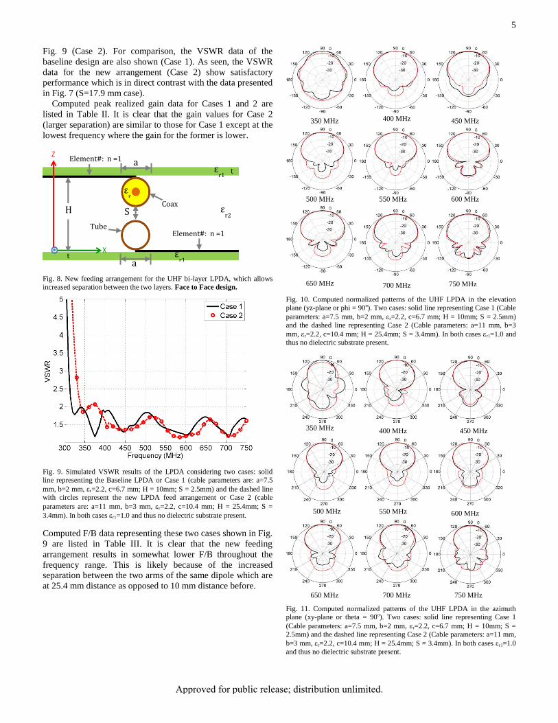
Fig. 9 (Case 2). For comparison, the VSWR data of the
baseline design are also shown (Case 1). As seen, the VSWR
data for the new arrangement (Case 2) show satisfactory
performance which is in direct contrast with the data presented
in Fig. 7 (S=17.9 mm case).
Computed peak realized gain data for Cases 1 and 2 are
listed in Table II. It is clear that the gain values for Case 2
(larger separation) are similar to those for Case 1 except at the
lowest frequency where the gain for the former is lower.
Fig. 8. New feeding arrangement for the UHF bi-layer LPDA, which allows
increased separation between the two layers. Face to Face design.
Fig. 9. Simulated VSWR results of the LPDA considering two cases: solid
line representing the Baseline LPDA or Case 1 (cable parameters are: a=7.5
mm, b=2 mm, r=2.2, c=6.7 mm; H = 10mm; S = 2.5mm) and the dashed line with circles represent the new LPDA feed arrangement or Case 2 (cable
parameters are: a=11 mm, b=3 mm, r=2.2, c=10.4 mm; H = 25.4mm; S =
3.4mm). In both cases r1=1.0 and thus no dielectric substrate present.
Computed F/B data representing these two cases shown in Fig.
9 are listed in Table III. It is clear that the new feeding
arrangement results in somewhat lower F/B throughout the
frequency range. This is likely because of the increased
separation between the two arms of the same dipole which are
at 25.4 mm distance as opposed to 10 mm distance before.
Fig. 10. Computed normalized patterns of the UHF LPDA in the elevation
plane (yz-plane or phi = 90o). Two cases: solid line representing Case 1 (Cable
parameters: a=7.5 mm, b=2 mm, r=2.2, c=6.7 mm; H = 10mm; S = 2.5mm)
and the dashed line representing Case 2 (Cable parameters: a=11 mm, b=3
mm, r=2.2, c=10.4 mm; H = 25.4mm; S = 3.4mm). In both cases r1=1.0 and thus no dielectric substrate present.
Fig. 11. Computed normalized patterns of the UHF LPDA in the azimuth plane (xy-plane or theta = 90o). Two cases: solid line representing Case 1
(Cable parameters: a=7.5 mm, b=2 mm, r=2.2, c=6.7 mm; H = 10mm; S =
2.5mm) and the dashed line representing Case 2 (Cable parameters: a=11 mm,
b=3 mm, r=2.2, c=10.4 mm; H = 25.4mm; S = 3.4mm). In both cases r1=1.0
and thus no dielectric substrate present.
H
a
S
Coax
Element#: n =1
Element#: n =1
a
Tube
εr1
εr1
t
εr2
εr
t
350 MHz 450 MHz 400 MHz
500 MHz 550 MHz 600 MHz
650 MHz 700 MHz 750 MHz
350 MHz 400 MHz 450 MHz
500 MHz 550 MHz 600 MHz
650 MHz 700 MHz 750 MHz
Approved for public release; distribution unlimited.

6
Nevertheless, except for the lowest frequency the F/B is
greater than 15 dB, which is satisfactory for most applications.
Computed normalized radiation patterns in the elevation and
azimuth planes for both cases are shown in Figs. 10 and 11.
The patterns are directional, and symmetric. Within the
frequency range of operation the half-power (3-dB)
beamwidths in the elevation plane ranges from 64 to 92
degrees while that in the azimuth plane ranges from 38 to 64
degrees.
V. SIMULATION RESULTS – SPACED BI-LAYER
DESIGN ON DIELECTRIC
Since the performance of the LPDA with the two layers
being separated by a distance, H=25.4 mm was found to be
satisfactory that design was considered for future fabrication
and characterization. Further considerations were to explore
the prospect of fabricating the array using a direct printing
technique through a commercial manufacturer [38]. The
commercial manufacturer spray prints antenna apertures and
transmission lines using their proprietary techniques where
they have specific dimensional limits and tolerances. Such as
trace widths have to be within certain standard sizes or custom
trace widths with small variations may become rather
expensive. Based on those available trace width dimensions
and the tolerances the UHF LPDA design was further adjusted
to maintain performance in the 350-750 MHz frequency band.
Those dimensions are only slightly different and are listed in
Table IV. Also since the array will be fabricated on dielectric
substrate materials the effect of dielectrics was also
investigated. These results are shown in Fig. 12 which shows
the VSWR data of the baseline design (original LPDA in free-
space), adjusted final LPDA in free-space to fit commercial
manufacturing trace width limits and tolerances, and the final
adjusted LPDA printed on thin (1.58 mm thick) FR4 substrate
layers. For the latter two cases H=25.4 mm and S=3.4 mm
while for the baseline case H=10 mm and S=2.5 mm. It is
clear that the final design with the adjusted dimensions and on
FR4 operates satisfactorily within the 350-750 MHz
bandwidth. The VSWR peaks are higher than the baseline
design but are still satisfactory.
Computed peak realized gain (dBi) and the F/B (dB) of the
final LPDA with adjusted dimensions and on thin FR4
substrates are listed in Table V. The gain varies between 6.2-9
dBi while the F/B varies between 5.3-19.1 dB.
Table II: Computed peak realized gain (dBi)of the UHF LPDA. In both cases r1=1.0 and thus no dielectric substrate present.
Frequency (MHz) 350 400 450 500 550 600 650 700 750
Case 1: H = 10 mm, S=2.5 mm, Gain
(dBi) 9.0 8.1 8.3 8.5 9.0 8.6 7.8 8.0 8.1
Case 2: H=25.4 mm, S=3.4 mm, Gain (dBi)
6.3 8.1 8.9 8.8 9.1 8.7 7.3 7.5 7.3
Table III: Computed Forward to Backward ratios (F/B) of the UHF LPDA. In both cases r1=1.0 and thus no dielectric substrate present.
Frequency (MHz) 350 400 450 500 550 600 650 700 750
Case 1: H = 10 mm, S=2.5 mm, F/B
(dB) 13.3 25.4 16.4 25.0 27.3 20.2 24.0 21.0 17.9
Case 2: H=25.4 mm, S=3.4 mm, F/B
(dB) 8.0 17.5 19.4 15.8 20.3 17.9 15.8 15.3 18.0
Table IV: Original and new trace widths.
Element #, n 1 2 3 4 5 6 7 8 9 10 11 12
Original Trace Width,
Tn (mm) 3.0 2.8 2.5 2.3 2.1 1.9 1.8 1.6 1.5 1.4 1.3 1.2
New Trace Width
(mm) 2.54 2.54 2.54 2.286 2.286 1.778 1.778 1.524 1.524 1.27 1.27 1.143
Table V: Computed peak realized gain (dBi) and F/B (dB) of the final adjusted dimensions LPDA on thin FR4 layers.
Frequency (MHz) 350 400 450 500 550 600 650 700 750
Array realized gain (dBi) for final LPDA on
FR4 6.2 7.8 9.0 8.4 8.7 8.6 7.0 7.8 7.1
Array F/B (dB) for final LPDA on FR4 5.3 12.2 18.3 19.1 19.1 17.7 15.2 11.2 15.6
Approved for public release; distribution unlimited.

7
Fig. 12. Simulated VSWR results of the LPDA considering three cases: solid
line representing the Baseline LPDA (cable parameters: a=7.5 mm, b=2 mm,
r=2.2, c=6.7 mm; H = 10mm; S = 2.5mm), the dashed line with circles represent the adjusted LPDA to meet commercial manufacturing trace width
limits and tolerances, and finally the dashed line with the plus signs represents
the adjusted LPDA on thin 1.58 mm FR4 layers. The latter two cases (a=11
mm, b=3 mm, r=2.2, c=10.4 mm; H = 25.4mm; S = 3.4 mm).
VI. EXPERIMENTAL RESULTS
The proposed UHF LPDA was fabricated in-house at the
University of South Carolina (USC) Microwave Engineering
Laboratory (MEL) using photochemical etching. As because
the complete array was about 3 ft long and 1 foot wide it was
not possible to etch such a large aperture using our existing
facilities. Instead, for each layer 12 inch by 12 inch 1.58 mm
thick FR4 substrates were used to build the whole array. The
two layers were separated from each other using plastic screws
that were placed away from the conducting elements of the
array. The array was fed using a 11 mm diameter coaxial cable
(LMR 600 cable from Times Microwaves) [37] and a
conducting copper tube. The outer insulation of the LMR 600
cable was removed in order to connect the antenna elements to
the outer shield of the coax. Photographs of the fabricated
array are shown in Fig. 13.
Fig. 13. Photographs of the fabricated LPDA.
Measured VSWR results of the fabricated LPDA are plotted
in Fig. 14, which show that the array operates from 350-750
MHz. The VSWR shows a slightly higher peak between 450-
500 MHz which is because of the difficulty in maintaining the
S=3.4 mm distance between the outer surface of the coax and
the tube that was maintained in the simulation models. It is
expected that in practical manufacturing more precise distance
control will be feasible either through better fixturing or
through the use of constant thickness low dielectric constant
insulating material.
Array radiation patterns and gain were measured in a
Satimo chamber at the Wireless Research Center of North
Carolina (WRCNC) [39]. Measured realized gain results are
shown in Fig. 15. It is clear that for much of the frequency
range the peak array gain is greater than 7 dBi. Only within a
narrow frequency range the array gain is near 6 dBi. The array
7 dBi gain bandwidth easily exceeds an octave of bandwidth
except for a narrow frequency range (660-670 MHz) where
the gain is 6.5 dBi.
Top Layer
Bottom Layer
Top Layer connection
Bottom Layer connection
Complete LPDA
Approved for public release; distribution unlimited.

8
Fig. 14. Measured VSWR of the UHF LPDA shown in Fig. 13.
Fig. 15. Measured peak realized gain of the UHF LPDA shown in Fig. 13.
Measured normalized radiation patterns of the UHF LPDA
shown in the photographs of Fig. 13 are shown in Figs. 16 and
17. The elevation plane patterns show directional beams with
Half-Power Beamwidths (HPBW) in the range of 72 to 114
degrees while the azimuth plane patterns show HPBWs in the
range of 54 to 72 degrees. The F/B ranges between 10-22 dB
with an average F/B of 15 dB. Thus the experimental results
clearly show a much higher F/B than the simulation results.
Table VI: Measured cross polarization at selected frequencies.
Frequency
(MHz)
400 450 500 550 600 650 700 750
Cross-pol (dB)
below
37.2 29.8 24.2 27.5 31.3 34.9 26.2 18
Measured cross-polarization data at selected frequencies are
listed in Table VI. Cross polarization at 350 MHz is 17.9 dB
(not listed in Table VI). Cross-polarization at most frequencies
is suppressed below 20 dB except at the band edges where it is
about 18 dB below the dominant polarization.
Fig. 16. Measured normalized Elevation Plane (phi = 90o) patterns of the
UHF LPDA shown in Fig. 12.
Fig. 17. Measured normalized azimuth plane (theta = 90o) patterns of the UHF LPDA shown in Fig. 12.
VI. CONCLUSION
The study, design, fabrication and characterization of a
broadband size-reduced UHF bi-layer CLAS LPDA are
presented. The use of a double meander dipole as the building
block allows a 30% reduction in the array width. Further
350 MHz 400 MHz 450 MHz
500 MHz 550 MHz 600 MHz
650 MHz 700 MHz 750 MHz
350 MHz 450 MHz 400 MHz
500 MHz 550 MHz 600 MHz
650 MHz 700 MHz 750 MHz
Approved for public release; distribution unlimited.

9
reduction is still possible as long as inter-element coupling
does not deteriorate the array performance. It is clearly
demonstrated that the two layers of the LPDA can be
sufficiently separated from each other (1 inch to 1.5 inch) for
the 350-750 MHz operation. The sensitivity of the array
VSWR and radiation properties on dielectric materials, cable
size, and cable orientation are studied. It is observed that a
symmetric feeding arrangement consisting of same diameter
cable and conducting tube with a small separation distance
between them is preferred. The presence of thin FR4 dielectric
materials has no significant detrimental effect on the array
performance except for the gain reduction due to the high loss
tangent of the FR4 material. Thus other low loss materials
such as RO4003 will be a better choice. The fabricated array
shows a VSWR bandwidth of 350-750 MHz. The gain of the
fabricated array is above 7 dBi for most of the operating
frequency band.
The design of the balanced feed line was a compromise to
satisfy the need that the two antenna layers be substantially
separated from each other. And thus the design depended on
the availability of a feed coax with proper diameter for 25.4
mm total separation. Moreover, the practical difficulty of
creating and maintaining a separation smaller than 3.4 mm in a
lab environment directed us toward the design with a balanced
line with higher characteristic impedance. Nevertheless, if one
can maintain a spacing ‘S’ of say 1 mm between the two
conductors of the feed line illustrated in Figs. 8 and 9 about
50 characteristic impedance can be obtained for the balanced
line. This will increase the gain between 0.5 to 1 dB
depending on the frequency.
The elevation and azimuth plane radiation patterns of the
array show well defined directional beams with high gain and
high F/B for most frequencies of operation. Further work will
be needed in order to design and tune the array to suit a
specific platform geometry and material system.
VII. REFERENCES
[1] R. Carrel, ‘The design of log-periodic dipole antennas,” IRE
International Convention Record., 1961, vol. 9, pp. 61-75.
[2] R. L. Carrel, “Analysis and design of the log-periodic dipole antenna,” University of Illinois Technical Report, No. 52, Urbana,
1961.
[3] V. H. Rumsey, Frequency Independent Antennas. New York: Academic Press, 1966.
[4] W.L. Stutzman and G.A. Thiele, Antenna Theory and Design, John
Wiley and Sons Inc., USA, 1998.
[5] P. B. Green and P. E. Mayes, “50 log-periodic monopole array
with modulated-impedance microstrip feeder,” IEEE Trans.
Antennas Propag., vol. AP-22, pp. 332-334, March 1974. [6] K. M. Keen, “A planar log-periodic antenna,” IEEE Trans.
Antennas Propag., vol. AP-22, pp. 489-490, May 1974.
[7] C.K. Campbell, I. Traboulay, M.S. Suthers, and H. Kneve, “Design of a Stripline Log Periodic Dipole Antenna,’’ IEEE Trans.
Antennas Propag., Vol. AP-25, pp. 718-721, Sept. 1977.
[8] R. R. Pantoja, A. R. Sapienza, and F. C. Medeirosfilho, “A Microwave Printed Planar Log-Periodic Dipole Array Antenna,’’
IEEE Trans. Antennas Propag., Vol. AP-35, pp. pp. 1176-1178,
Oct. 1987. [9] A. A. Gheethan and D. E. Anagnostou, “The Design and
Optimization of Planar LPDAs,’’ PIERS Proceedings, Cambridge,
USA, July 2008, pp. 478-481. [10] D. Anagnostou, J. Papapolymerou, M.M. Tentzeris, and C.G.
Christodoulou, “A Printed Log-Periodic Koch-Dipole Array
(LPKDA),’’ IEEE Antennas and Wireless Propagat. Lett., Vol. 7,
2008, pp. 456-460. [11] F. Merli, J.-F. Zürcher, A. Freni, and A.K. Skrivervik, “Analysis,
design and realization of a novel directive ultrawideband
antenna,’’ IEEE Trans. Antennas Propag., Vol. 57, pp. 3458-3466, Nov. 2009.
[12] A. Calmon, G. Pacheco, M.A.B. Terada, “A novel reconfigurable
UWB log-periodic antenna,’’ IEEE Antennas and Propagation Society Interntaional Symp. Dig., 2006, pp. 213-216.
[13] A. Khaleghi, H.S. Farahani, and I. Balasingham, “Impulse
Radiating Log-Periodic Dipole Array Antenna Using Time-Reversal Technique,’’ IEEE Antennas and Wireless Propagat.
Lett., Vol. 10, 2011, pp. 967-970.
[14] C. Yu, W. Hong, L. Chiu, G. Zhai, C. Yu, W. Qin, and Z. Kuai, “Ultrawideband Printed Log-Periodic Dipole Antenna With
Multiple Notched Bands,’’ IEEE Trans. Antennas Propag., Vol.
59, pp. 725-732, Mar. 2011. [15] G.A. Casula, P. Maxia, and G. Mazzarella, “A printed LPDA with
UWB capability,’’ 2010 International Workshop on Antenna
Technology (IWAT), pp. 1.4. [16] L. Shan, L. Xiaofeng, Q. Jinghui, “A novel miniaturized ultra
wideband log-periodic antenna,’’ 2010 International Conference
on Ultrawideband and Ultrashort Impulse Signals (UWBUSIS), pp. 246-248.
[17] B. Turetken, “Design and realization of printed LPDA in UHF
band,’’ 10th International Conference on Mathematical Methods in Electromagnetic Theory, 2004., Sept. 14-17, 2004, pp. 295 –
297. [18] M. N. A. Karim, M. K. A. Rahim, H. A. Majid, O. Ayop, M. Abu
and F. Zubir, “Log periodic fractal Koch Antenna for UHF band
applications,’’ Progress In Electromagnetics Research, PIER 100, 201-218, 2010.
[19] P. Li, X. Jiang, X. Liu, H. Shi, X. Lu, “Research on the relation
between Printed Log-Periodic Antenna's feed and bandwidth,’’ 2010 International Symposium on Signals Systems and Electronics,
pp. 1-3.
[20] A. Moallemizadeh, H.R. Hassani, and S.M.A. Nezhad, “Wide bandwidth and small size LPDA antenna,’’ 2012 6th European
Conference on Antennas and Propagation (EUCAP), pp. 1-3.
[21] B. Gong, L.H. Su, Y.-Z. Yin, H. Ma, Q.-R. Zheng, “A novel log-periodic dipole antenna with distributed inductive load,’’ 2012 2nd
International Conference on Consumer Electronics,
Communications and Networks (CECNet), pp. 61 – 63. [22] X.L. Zhang and H.-T. Gao, “An optimum design of miniaturized
high frequency inverted-V log-periodic dipole antenna,’’ 2011
IEEE CIE International Conference on Radar (Radar), pp. 1185 – 1188.
[23] Q. Zhao and Z. Yin, “The influence of feed tube changes on
performance of log periodic dipole antenna,’’ 2012 International Conference on Microwave and Millimeter Wave Technology
(ICMMT), pp. 1 – 4. [24] H. Zhou, N.A. Sutton, and D.S. Filipovic, “W-band endfire log
periodic dipole array,’’ 2011 IEEE International Symposium on
Antennas and Propagation (APSURSI), pp. 1233 – 1236. [25] J.-M. Lee, H.-J. Ham, H.-K. Ryu , J.-M. Woo, B.-J. Park, K.-S.
Lee, “Miniaturization of log-periodic dipole array antenna using
triangular meander structure,’’ 2012 IEEE International
Conference on Wireless Information Technology and Systems (ICWITS), pp. 1 – 4.
[26] D.N. West and S.K. Sharma, “Frequency reconfigurable compact
multiband quasi-log periodic dipole array (QLPDA) antenna for wireless communications,’’ 2010 IEEE Antennas and Propagation
Society International Symposium (APSURSI), pp. 1 – 4.
[27] M. Hilbert, M.A. Tilston, and K.G. Balmain, “Resonance phenomena of log-periodic antennas: characteristic-mode
analysis,’’ IEEE Trans. Antennas Propag., Vol. 37. pp. 1224-1234,
1989. [28] Hyperlog 7040 [online available: http://www.aaronia.com/?id=6
[29] M.A. Hopkins, J.M. Tuss, A.J. Lockyer, J.N. Kudva, “Smart Skin
Conformal Load-Bearing Antenna and Other Smart Structure Developments,’’ Nato Workshop on Smart Electromagnetic
Structures, 25-26 Nov. 1996. [30] A.J. Lockyer, K.H. Alt, R.W. Kinslow, H.-P. Kan, J.N. Kudva,
J.M. Tuss, and A.C. Goetz, “Development of a structurally
integrated conformal load-bearing multifunction antenna: overview
Approved for public release; distribution unlimited.
10
of the Air Force Smart Skin Structures Technology Demonstration
Program,’’ Proc. SPIE 2722, Smart Structures and Materials 1996: Smart Electronics and MEMS, 55 (May 20, 1996).
[31] A.J. Lockyer, K.H. Alt, J.N. Kudva, R.W. Kinslow, A.Goetz,
“Conformal load-bearing antenna structures (CLAS): Initiative for multiple military and commercial applications,’’ SPIE Vol. 3046,
pp.182-196, 1997.
[32] C. You, M.M. Tentzeris, and W. Hwang, “Multilayer Effects on Microstrip Antennas for Their Integration With Mechanical
Structure,’’ IEEE Trans. Antennas Propagat., vol. 55, Apr. 2007,
pp. 1051-1058. [33] M. Ali, Analyses of Self-Resonant Bent Antennas, Ph.D.
Dissertation, University of Victoria, BC, Canada, 1997.
[34] M. Ali, S.S. Stuchly, and K. Caputa, “A Wide-Band Dual Meander-Sleeve Antenna, ”Journal of Electromagnetic Waves and
Applications, Vol. 10, No. 9, 1996, pp. 1223-1236.
[35] M. Ali, G.J. Hayes, H.-S. Hwang and R.A. Sadler, “Design of a Multi--Band Internal Antenna for Third Generation Mobile Phone
Handsets,” ’’ IEEE Trans. Antennas Propag., vol. 51, no. 7, July
2003, pp. 1452-1461. [36] C.A. Balanis, Antenna Theory Analysis and Design, John Wiley
and Sons, USA, Third Edition.
[37] Times Microwaves Inc. USA. online available: [http://www.timesmicrowave.com/].
[38] Mesoscribe Technologies Inc. USA. online available:
[http://www.mesoscribe.com/services/direct-write-fabrication/]. [39] Wireless Research Center of North Carolina (WRCNC); online
available: [http://www.wirelesscenter-nc.org/].
Approved for public release; distribution unlimited.