AFRL-PR-WP-TR-2006-2181 - apps.dtic.mil · Taguchi 3k factorial design for wire bonding DOE Table...
111
AFRL-PR-WP-TR-2006-2181 CONTACT METALLIZATION AND PACKAGING TECHNOLOGY DEVELOPMENT FOR SiC BIPOLAR JUNCTION TRANSISTORS, PiN DIODES, AND SCHOTTKY DIODES DESIGNED FOR LONG-TERM OPERATIONS AT 350ºC J.R. Williams (Physics Department) and R.W. Johnson Auburn University Space Research Institute 231 Leach Science Center Auburn University, AL 36849 S.E. Mohney The Pennsylvania State University S.-H. Ryu Cree, Inc. MAY 2006 Final Report for 01 November 2001 – 31 May 2006 Approved for public release; distribution is unlimited. STINFO COPY PROPULSION DIRECTORATE AIR FORCE MATERIEL COMMAND AIR FORCE RESEARCH LABORATORY WRIGHT-PATTERSON AIR FORCE BASE, OH 45433-7251
Transcript of AFRL-PR-WP-TR-2006-2181 - apps.dtic.mil · Taguchi 3k factorial design for wire bonding DOE Table...

AFRL-PR-WP-TR-2006-2181
CONTACT METALLIZATION AND PACKAGING TECHNOLOGY DEVELOPMENT FOR SiC BIPOLAR JUNCTION TRANSISTORS, PiN DIODES, AND SCHOTTKY DIODES DESIGNED FOR LONG-TERM OPERATIONS AT 350ºC J.R. Williams (Physics Department) and R.W. Johnson Auburn University Space Research Institute 231 Leach Science Center Auburn University, AL 36849 S.E. Mohney The Pennsylvania State University S.-H. Ryu Cree, Inc. MAY 2006 Final Report for 01 November 2001 – 31 May 2006
Approved for public release; distribution is unlimited.
STINFO COPY
PROPULSION DIRECTORATE AIR FORCE MATERIEL COMMAND AIR FORCE RESEARCH LABORATORY WRIGHT-PATTERSON AIR FORCE BASE, OH 45433-7251

NOTICE AND SIGNATURE PAGE Using Government drawings, specifications, or other data included in this document for any purpose other than Government procurement does not in any way obligate the U.S. Government. The fact that the Government formulated or supplied the drawings, specifications, or other data does not license the holder or any other person or corporation; or convey any rights or permission to manufacture, use, or sell any patented invention that may relate to them. This report was cleared for public release by the Air Force Research Laboratory Wright Site (AFRL/WS) Public Affairs Office and is available to the general public, including foreign nationals. Copies may be obtained from the Defense Technical Information Center (DTIC) (http://www.dtic.mil). AFRL-PR-WP-TR-2006-2181 HAS BEEN REVIEWED AND IS APPROVED FOR PUBLICATION IN ACCORDANCE WITH ASSIGNED DISTRIBUTION STATEMENT. *//Signature// //Signature// JAMES D. SCOFIELD, Ph.D. JOSEPH A. WEIMER Project Engineer Chief, Electrical Technology Branch Electrical Technology Branch Power Division Power Division //Signature// KIRK L. YERKES, Ph.D. Deputy for Science Power Division This report is published in the interest of scientific and technical information exchange, and its publication does not constitute the Government’s approval or disapproval of its ideas or findings. *Disseminated copies will show “//Signature//” stamped or typed above the signature blocks.

i
REPORT DOCUMENTATION PAGE Form Approved OMB No. 0704-0188
The public reporting burden for this collection of information is estimated to average 1 hour per response, including the time for reviewing instructions, searching existing data sources, searching existing data sources, gathering and maintaining the data needed, and completing and reviewing the collection of information. Send comments regarding this burden estimate or any other aspect of this collection of information, including suggestions for reducing this burden, to Department of Defense, Washington Headquarters Services, Directorate for Information Operations and Reports (0704-0188), 1215 Jefferson Davis Highway, Suite 1204, Arlington, VA 22202-4302. Respondents should be aware that notwithstanding any other provision of law, no person shall be subject to any penalty for failing to comply with a collection of information if it does not display a currently valid OMB control number. PLEASE DO NOT RETURN YOUR FORM TO THE ABOVE ADDRESS.
1. REPORT DATE (DD-MM-YY) 2. REPORT TYPE 3. DATES COVERED (From - To)
May 2006 Final 11/01/2001 – 05/31/2006 5a. CONTRACT NUMBER
F33615-01-C-2188 5b. GRANT NUMBER
4. TITLE AND SUBTITLE
CONTACT METALLIZATION AND PACKAGING TECHNOLOGY DEVELOPMENT FOR SiC BIPOLAR JUNCTION TRANSISTORS, PiN DIODES, AND SCHOTTKY DIODES DESIGNED FOR LONG-TERM OPERATIONS AT 350ºC
5c. PROGRAM ELEMENT NUMBER 62203F
5d. PROJECT NUMBER
3145 5e. TASK NUMBER
13
6. AUTHOR(S)
J.R. Williams (Physics Department of Auburn University) and R.W. Johnson (Auburn University) S.E. Mohney (The Pennsylvania State University) S.-H. Ryu (Cree, Inc.)
5f. WORK UNIT NUMBER
0B 7. PERFORMING ORGANIZATION NAME(S) AND ADDRESS(ES) 8. PERFORMING ORGANIZATION
REPORT NUMBER
Auburn University Space Research Institute 231 Leach Science Center Auburn University, AL 36849
The Pennsylvania State University ----------------------------------------------------
Cree, Inc.
9. SPONSORING/MONITORING AGENCY NAME(S) AND ADDRESS(ES) 10. SPONSORING/MONITORING AGENCY ACRONYM(S)
AFRL-PR-WP Propulsion Directorate Air Force Research Laboratory Air Force Materiel Command Wright-Patterson AFB, OH 45433-7251
11. SPONSORING/MONITORING AGENCY REPORT NUMBER(S) AFRL-PR-WP-TR-2006-2181
12. DISTRIBUTION/AVAILABILITY STATEMENT Approved for public release; distribution is unlimited.
13. SUPPLEMENTARY NOTES PAO case number: AFRL/WS 06-1575; Date cleared: 21 June 2006. This report contains color.
14. ABSTRACT
This report describes the development of composite ohmic contact and packaging technologies for the wide band gap semiconductor silicon carbide (SiC) with demonstrations of these technologies using 4H-SiC JFETs (junction field effect transistors). The goal of this effort is protection against oxidation / inter-diffusion and stable operation in air at 350 °C for up to 10,000 hr. Ta-Si and Ru-Ta barrier layers have been developed and tested for composite contacts that consist of the ohmic contact layer (e.g., Ni2Si), the barrier layer, an adhesion layer such as Pt and a gold cap layer that is suitable for wire bonding. Reliability and failure analysis studies have been conducted for chip metallizations for die attachment and for large area wire bonding to substrate metals, die metals and die metals over SiO2. 1800V/5A 4H-SiC JEFETs have been designed and fabricated using the Ta-Si and Ru-Ta barrier layers in the composite ohmic contacts. The devices were characterized at 300 °C and used in the design of a 2W, 270-28V dc-dc converter. With Vgate = -33V, the JFETs were able to block 600V with J < 32microamps/sq cm at 300 °C
15. SUBJECT TERMS
16. SECURITY CLASSIFICATION OF: 19a. NAME OF RESPONSIBLE PERSON (Monitor) a. REPORT Unclassified
b. ABSTRACT Unclassified
c. THIS PAGE Unclassified
17. LIMITATION OF ABSTRACT:
SAR
18. NUMBER OF PAGES
116 James D. Scofield 19b. TELEPHONE NUMBER (Include Area Code)
N/A
Standard Form 298 (Rev. 8-98) Prescribed by ANSI Std. Z39-18

iii
Table of Contents
Figures & Tables: Section 2: Composite High Temperature Ohmic Contacts to 4H-SiC v Section 3: SiC Power Device Packaging vii Section 4: Devices xi Acknowledgments xii 1. Summary 1
2. Composite High Temperature Ohmic Contacts to 4H-SiC 2
2.1 Introduction 2
2.2 Ta-Si-N – based Composite Ohmic Contacts 2
Choice of Oxidation/Barrier Layer 2
Composite Contact Fabrication and Electrical Characterization 5
Mechanical Characterization 8
Conclusions 10
2.3 Ru-Ta – based Composite Ohmic contacts 11
General Information 11
Tantalum-Ruthenium-Nitrogen Diffusion Barriers 11
Tantalum-Ruthenium Diffusion Barriers 19
Conclusions 24
3. SiC Power Device Packaging 25
3.1 Introduction 25
3.2 Die Attach for SiC 26
Chip Metallization 27
Die Attach 28
3.2.1 Reliability Testing 36
High Temperature Storage Tests 36
Thermal Cycle Tests 43
Conclusions 53
3.3 Large Diameter Wire Bonds to Die Metallizations 54
3.3.1 Large Diameter Wire Bond to Substrate Metal 54

iv
Bonding Parameters 54
Accelerated Aging Tests 59
3.3.2 Large Diameter Wire Bond to Die Metal Over SiO2 61
Wire Bond Parameters 61
Accelerated Aging Tests 61
Failure Analysis 64
3.3.3 Large Diameter Wire Bond to Die Metal Without SiO2 73
Accelerated Aging Tests 73
3.3.4 Conclusions 74
3.4 Characterization of High Temperature Electrical Insulation Polymers 74
3.4.1 Polyimide 75
Test Sample Fabrication and Experiment Set-up 75
Experimental Results 77
3.4.2 Modified Polyimide 78
3.4.3 Phthalonitrile 79
3.4.4 Conclusions 80
4. Devices: Normally-on, High Temperature 4H-SiC Junction Field
Effect Transistors 80
4.1 Introduction 80
4.2 Development of 4H-SiC JFETs for High Temperature Operation 81
4.3 Conclusions 93
5. References 94
6. Appendix: Students Graduated and Publications/Presentations 96
v
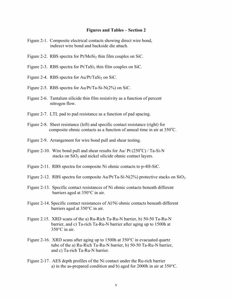
Figures and Tables – Section 2 Figure 2-1. Composite electrical contacts showing direct wire bond, indirect wire bond and backside die attach. Figure 2-2. RBS spectra for Pt/MoSi2 thin film couples on SiC. Figure 2-3. RBS spectra for Pt/TaSi2 thin film couples on SiC. Figure 2-4. RBS spectra for Au/Pt/TaSi2 on SiC. Figure 2-5. RBS spectra for Au/Pt/Ta-Si-N(2%) on SiC. Figure 2-6. Tantalum silicide thin film resistivity as a function of percent nitrogen flow. Figure 2-7. LTL pad to pad resistance as a function of pad spacing. Figure 2-8. Sheet resistance (left) and specific contact resistance (right) for composite ohmic contacts as a function of anneal time in air at 350oC. Figure 2-9. Arrangement for wire bond pull and shear testing. Figure 2-10. Wire bond pull and shear results for Au/ Pt (250oC) / Ta-Si-N stacks on SiO2 and nickel silicide ohmic contact layers. Figure 2-11. RBS spectra for composite Ni ohmic contacts to p-4H-SiC. Figure 2-12. RBS spectra for composite Au/Pt/Ta-Si-N(2%) protective stacks on SiO2. Figure 2-13. Specific contact resistances of Ni ohmic contacts beneath different barriers aged at 350°C in air. Figure 2-14. Specific contact resistances of Al/Ni ohmic contacts beneath different barriers aged at 350°C in air. Figure 2.15. XRD scans of the a) Ru-Rich Ta-Ru-N barrier, b) 50-50 Ta-Ru-N barrier, and c) Ta-rich Ta-Ru-N barrier after aging up to 1500h at 350°C in air. Figure 2-16. XRD scans after aging up to 1500h at 350°C in evacuated quartz tube of the a) Ru-Rich Ta-Ru-N barrier, b) 50-50 Ta-Ru-N barrier, and c) Ta-rich Ta-Ru-N barrier. Figure 2-17. AES depth profiles of the Ni contact under the Ru-rich barrier a) in the as-prepared condition and b) aged for 2000h in air at 350°C.
vi
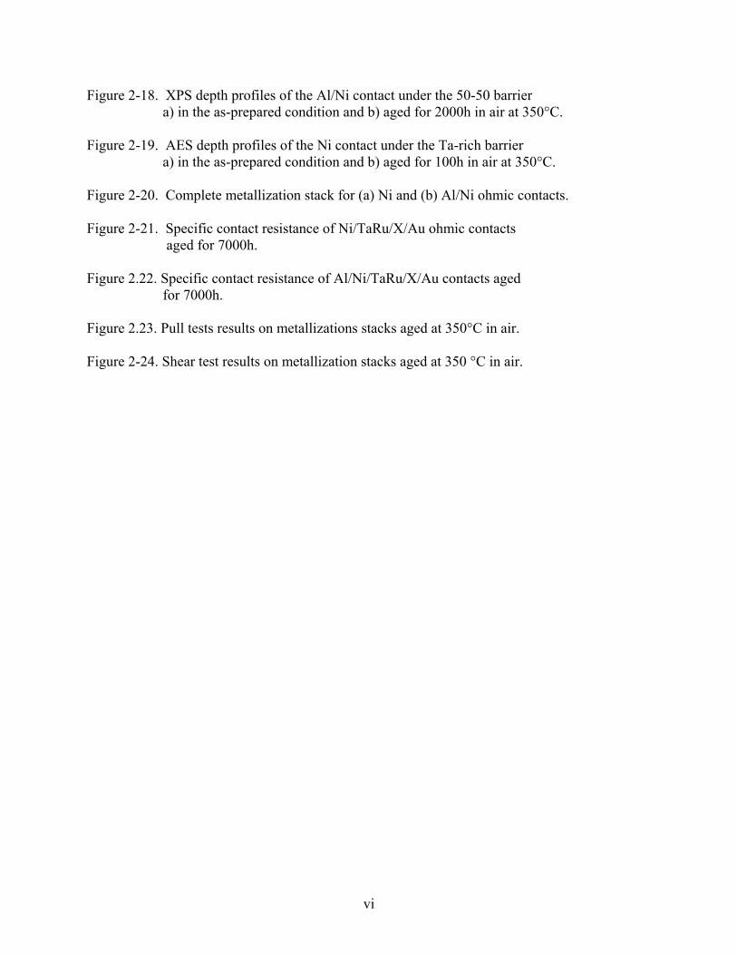
Figure 2-18. XPS depth profiles of the Al/Ni contact under the 50-50 barrier a) in the as-prepared condition and b) aged for 2000h in air at 350°C. Figure 2-19. AES depth profiles of the Ni contact under the Ta-rich barrier a) in the as-prepared condition and b) aged for 100h in air at 350°C. Figure 2-20. Complete metallization stack for (a) Ni and (b) Al/Ni ohmic contacts. Figure 2-21. Specific contact resistance of Ni/TaRu/X/Au ohmic contacts aged for 7000h. Figure 2.22. Specific contact resistance of Al/Ni/TaRu/X/Au contacts aged for 7000h. Figure 2.23. Pull tests results on metallizations stacks aged at 350°C in air. Figure 2-24. Shear test results on metallization stacks aged at 350 °C in air.
vii
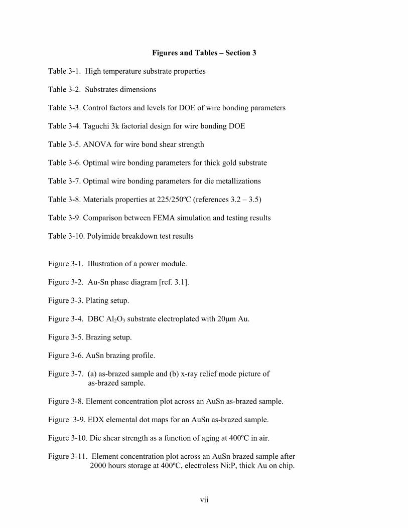
Figures and Tables – Section 3 Table 3-1. High temperature substrate properties Table 3-2. Substrates dimensions Table 3-3. Control factors and levels for DOE of wire bonding parameters Table 3-4. Taguchi 3k factorial design for wire bonding DOE Table 3-5. ANOVA for wire bond shear strength Table 3-6. Optimal wire bonding parameters for thick gold substrate Table 3-7. Optimal wire bonding parameters for die metallizations Table 3-8. Materials properties at 225/250ºC (references 3.2 – 3.5) Table 3-9. Comparison between FEMA simulation and testing results Table 3-10. Polyimide breakdown test results Figure 3-1. Illustration of a power module. Figure 3-2. Au-Sn phase diagram [ref. 3.1]. Figure 3-3. Plating setup. Figure 3-4. DBC Al2O3 substrate electroplated with 20μm Au. Figure 3-5. Brazing setup. Figure 3-6. AuSn brazing profile. Figure 3-7. (a) as-brazed sample and (b) x-ray relief mode picture of as-brazed sample. Figure 3-8. Element concentration plot across an AuSn as-brazed sample. Figure 3-9. EDX elemental dot maps for an AuSn as-brazed sample. Figure 3-10. Die shear strength as a function of aging at 400ºC in air. Figure 3-11. Element concentration plot across an AuSn brazed sample after 2000 hours storage at 400ºC, electroless Ni:P, thick Au on chip.

viii
Figure 3-12. Cross-section of die attach after 2000 hours at 400ºC, electroless Ni:P, thick Au on chip, (a) at Ni:P:Cu broken area and (b) at Ni:P:Cu continuous area. Figure 3-13. Cross-section of the die attach, (a) voids at Cu-Ni:P interface after 1000 hours aging and (b) cracks at Cu-Ni:P interface after 2000 hours aging at 400ºC. Figure 3-14. Element concentration plot across an AuSn brazed sample after 2000 hours storage at 400ºC; electrolytic Ni, thick Au on substrate. Figure 3-15. Cross-section of die attach after 2000 hours at 400ºC, electrolytic Ni, thick Au on substrate. Figure 3-16. Cross-section of the die attach, showing voids at Cu-Ni interface after 2000 hours aging at 400ºC. Figure 3-17. Die shear strength as a function of aging, confirmation test, 6 µm Ni DBC Al2O3 substrates, 400ºC in air. Figure 3-18. Die shear strength as a function of aging, confirmation test, 1μm Ni DBC Al2O3 substrates, 400ºC in air. Figure 3-19. Thermal cycle test profile. Figure 3-20. Die shear strength as a function of thermal cycle numbers. Figure 3-21. AES results after 100 thermal cycles, DBC Al2O3 substrate with 1μm electroless Ni:P, (a) Cu foil surface and (b) substrate surface. Figure 3-22. Cross-section of braze layer after 100 thermal cycles, showing crack in braze layer and braze-TiW delamination. DBC Al2O3 with 1μm electrolytic Ni. Figure 3-23. Cu foil delamination after 250 thermal cycles. Figure 3-25. Cross-section of braze layer after 250 thermal cycles. Figure 3-26. Cross-section of braze layer after 250 thermal cycles. Figure 3-27. (a) X-ray image in relief mode, showing cracks in the braze layer and (b) x-ray image in voids calculation mode. Figure 3-28. AES results after 250 thermal cycles, DBC Al2O3 with 6μm electroless Ni:P, (a) substrate side and (b) chip side. Figure 3-29. Si3N4 assembly after 500 cycles, showing the Cu foil delamination.

ix
Figure 3-30. AES results of Si3N4 substrate after 500 thermal cycles, (a) Cu foil surface and (b) substrate surface. Figure 3-31. Cross-section of the braze layer after 500 thermal cycles, showing cracks in the braze layer and braze-TiW delamination. Figure 3-32. (a) X-ray image in relief mode, showing cracks in the braze layer and (b) x-ray image in voids calculation mode. Figure 3-33. AlN substrate after 100 thermal cycles, (a) side with blistering and (b) side without blistering. Figure 3-34. Illustration of the perfect bond (Orthodyne Model 360B Operator Manuel). Figure 3-35. Photograph of a real bond. Figure 3-36. Main Effects Plot for means based on shear strength. Figure 3-37. Average pull/shear strength of gold wire on substrate metallization. Figure 3-38. Average pull/shear strength of platinum wire on substrate metallization. Figure 3-39. Average pull/shear strength of Au wire on Ti/TiW/Au metallization. Figure 3-40. SiO2 under Ti/Pt/Au without and with wire bond after 200 hour aging. Figure 3-41. Left - Ti/Pt deformation after the Au layer has been etched off. Figure 3-42. Bond head movement (Orthodyne 360B Operating Manual). Figure 3-43. Bond pad metallization 2D model. Figure 3-44. Pad metallization mesh and load. Figure 3-45. Von Mises stress in Ti/TiW/Au metallization for Au wire bonding. Figure 3-46. Von Mises strain in Ti/TiW/Au metallization for Au wire bonding. Figure 3-47. Von Mises stress in Ti/Pt/Au metallization for Au wire bonding. Figure 3-48. Von Mises strain in Ti/Pt/Au metallization for Au wire bonding. Figure 3-49. Von Mises stress in Ti/TiW/Au metallization for Pt wire bonding. Figure 3-50. Von Mises strain in Ti/TiW/Au metallization for Pt wire bonding. Figure 3-51. Von Mises stress in Ti/Pt/Au metallization for Pt wire bonding.

x
Figure 3-52. Von Mises strain in Ti/Pt/Au metallization for Pt wire bonding. Figure 3-53. Average shear/pull strength of gold wire bonds on Ta-Si-N 92%)/Pt-N/Au. Figure 3-54. Polyimide breakdown testing sample pattern. Figure 3-55. Polyimide PI2611 curing profile. Figure 3-56. Polyimide breakdown measurement circuit schematic. Figure 3-57. Breakdown strength at 300oC for POSS-modified PI2611 thermally aged at 300ºC. Figure 3-58. Breakdown strength for PT thermally aged at 300ºC.
xi
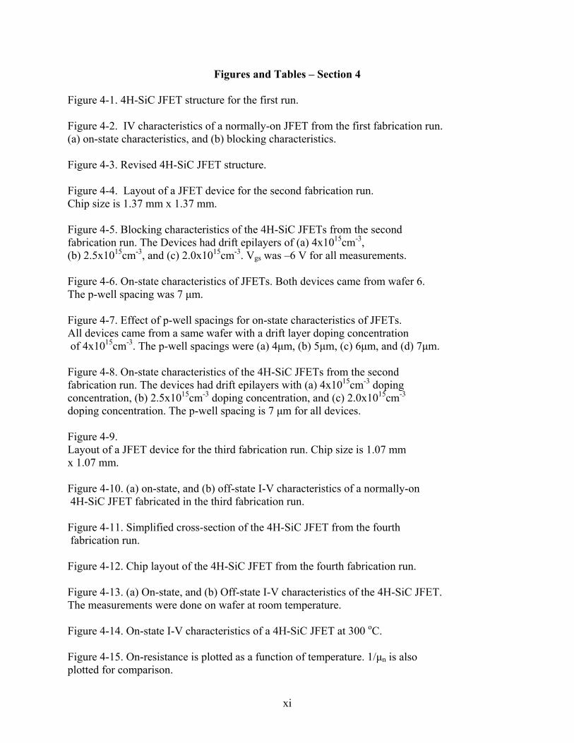
Figures and Tables – Section 4 Figure 4-1. 4H-SiC JFET structure for the first run. Figure 4-2. IV characteristics of a normally-on JFET from the first fabrication run. (a) on-state characteristics, and (b) blocking characteristics. Figure 4-3. Revised 4H-SiC JFET structure. Figure 4-4. Layout of a JFET device for the second fabrication run. Chip size is 1.37 mm x 1.37 mm. Figure 4-5. Blocking characteristics of the 4H-SiC JFETs from the second fabrication run. The Devices had drift epilayers of (a) 4x1015cm-3, (b) 2.5x1015cm-3, and (c) 2.0x1015cm-3. Vgs was –6 V for all measurements. Figure 4-6. On-state characteristics of JFETs. Both devices came from wafer 6. The p-well spacing was 7 μm. Figure 4-7. Effect of p-well spacings for on-state characteristics of JFETs. All devices came from a same wafer with a drift layer doping concentration of 4x1015cm-3. The p-well spacings were (a) 4μm, (b) 5μm, (c) 6μm, and (d) 7μm. Figure 4-8. On-state characteristics of the 4H-SiC JFETs from the second fabrication run. The devices had drift epilayers with (a) 4x1015cm-3 doping concentration, (b) 2.5x1015cm-3 doping concentration, and (c) 2.0x1015cm-3 doping concentration. The p-well spacing is 7 μm for all devices. Figure 4-9. Layout of a JFET device for the third fabrication run. Chip size is 1.07 mm x 1.07 mm. Figure 4-10. (a) on-state, and (b) off-state I-V characteristics of a normally-on 4H-SiC JFET fabricated in the third fabrication run. Figure 4-11. Simplified cross-section of the 4H-SiC JFET from the fourth fabrication run. Figure 4-12. Chip layout of the 4H-SiC JFET from the fourth fabrication run. Figure 4-13. (a) On-state, and (b) Off-state I-V characteristics of the 4H-SiC JFET. The measurements were done on wafer at room temperature. Figure 4-14. On-state I-V characteristics of a 4H-SiC JFET at 300 oC. Figure 4-15. On-resistance is plotted as a function of temperature. 1/μn is also plotted for comparison.
xii
Figure 4-16. Pinch off voltage and transconductance plotted as functions of temperature. Figure 4-17. Leakage current as a function of temperature. A maximum drain bias of 600 V was used, and a VGS of –33 V was used. Figure 4-18. Current and voltage waveforms for one of the 4H-SiC JFET low-side switches in the converter H-bridge, at 35, 200, and 304oC. Figure 4-19. (a) on-state and blocking conduction losses as f(T), including decreasing mobility trend due to acoustic phonon scattering mechanism, and (b) dynamic loss data as f(T) for JFET turn-on and turn-off. Figure 4-20. Turn-on and turn-off waveforms of the SiC JFET H-bridge low-side switch 35 and 304oC.

xiii
Acknowledgements The authors would like to thank the Air Force Research Laboratory for its support of the work undertaken for this project over the past four years. We wish particularly to express our appreciation to Dr. James D. Scofield of the AFRL, not only for his assistance with the administrative aspects of the project, but also for his active involvement in a number of the experimental measurements that produced results that are included in this report.
1
1. Summary
Wide band gap electronic materials and devices are of genuine interest to the Department of Defense where advanced, high performance devices and circuits are needed for operation in harsh environments with minimal cooling. Silicon carbide is the most advanced semiconductor in the wbg family that also includes diamond and the group III-nitrides, and SiC discrete device development is now underway worldwide.
Contractors supporting Air Force programs require wide band gap power device and
component solutions for More Electric, Space Platform and Direct Energy missions. A near-term goal for the Air Force is development of advanced motor drives for flight control and space vehicle applications, and converters / inverters for power conditioning applications in more electric and directed energy systems. Diodes and transistors are the basic components in semiconductor switches that are used in power conditioning systems. Silicon carbide diodes are now available commercially, and transistors (JEFETs, MOSFETs, IGBTs) are expected within the next few years. Crucial to the success of these devices for Air Force requirements is the development of advanced metallization and packaging technologies that will allow power devices to be used under extreme conditions.
The goal of our program over the past four years has been the development of an
advanced SiC metallization / packaging technology that survives long-term, high temperature operation in air, with demonstrations of the technology planned originally for 4H-SiC diodes and bipolar junction transistors designed for specific current / voltage requirements. The decision was made at a review meeting early in the program to instead use 4H-SiC JFETs as the demonstration device. We have sought to demonstrate less than 10% degradation in the performance of the metallization / packaging schemes after operation in air at 350oC for up to 10,000hr.
Section 2 of this report describes the development of oxidation / diffusion barrier layers
that are used for composite ohmic contact fabrication. In a composite contact (Figure 2-1), the barrier layer is sandwiched between the ohmic contact layer and a cap layer that is suitable for wire bonding or brazing. Two barrier layers are described in Section 2 – one based on Ta-Si-N and a second based on Ru-Ta.
Section 3 presents the results of studies in three packaging areas: (1) die attach for 4H-
SiC (chip metallization, die attach and reliability testing), (2) large diameter wire bonding to substrate metalizations, die metalizations and die metalizations over SiO2, and (3) high temperature insulating polymers.
Section 4 describes the design, fabrication and scale-up of 4H-SiC JEFETs. These
transistors were fabricated with the barrier layers described in Section 2. In their final configuration, these devices block 1800V at room temperature. At 300oC, the JFETs are able to block 600V with off-state (Vgate = -33V) current densities of less than 32μamp/cm2.
2
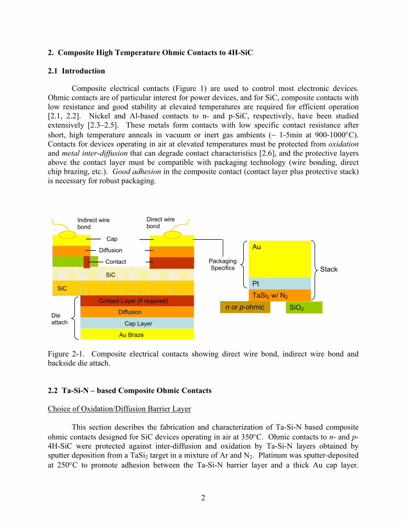
2. Composite High Temperature Ohmic Contacts to 4H-SiC 2.1 Introduction Composite electrical contacts (Figure 1) are used to control most electronic devices. Ohmic contacts are of particular interest for power devices, and for SiC, composite contacts with low resistance and good stability at elevated temperatures are required for efficient operation [2.1, 2.2]. Nickel and Al-based contacts to n- and p-SiC, respectively, have been studied extensively [2.3–2.5]. These metals form contacts with low specific contact resistance after short, high temperature anneals in vacuum or inert gas ambients (~ 1-5min at 900-1000°C). Contacts for devices operating in air at elevated temperatures must be protected from oxidation and metal inter-diffusion that can degrade contact characteristics [2.6], and the protective layers above the contact layer must be compatible with packaging technology (wire bonding, direct chip brazing, etc.). Good adhesion in the composite contact (contact layer plus protective stack) is necessary for robust packaging.
Figure 2-1. Composite electrical contacts showing direct wire bond, indirect wire bond and backside die attach. 2.2 Ta-Si-N – based Composite Ohmic Contacts Choice of Oxidation/Diffusion Barrier Layer This section describes the fabrication and characterization of Ta-Si-N based composite ohmic contacts designed for SiC devices operating in air at 350°C. Ohmic contacts to n- and p-4H-SiC were protected against inter-diffusion and oxidation by Ta-Si-N layers obtained by sputter deposition from a TaSi2 target in a mixture of Ar and N2. Platinum was sputter-deposited at 250°C to promote adhesion between the Ta-Si-N barrier layer and a thick Au cap layer.
Contact
SiC
Diffusion
Cap
SiC
Contact Layer (if required)
Au Braze
Diffusion
Cap Layer
Au
Pt
TaSi2 w/ N2
n or p-ohmic SiO2
Packaging Specifics Stack
Die attach
Indirect wire bond
Direct wire bond
3
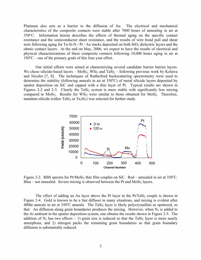
Platinum also acts as a barrier to the diffusion of Au. The electrical and mechanical characteristics of the composite contacts were stable after 7000 hours of annealing in air at 350°C. Information herein describes the effects of thermal aging on the specific contact resistance and the semiconductor sheet resistance, and the results of wire bond pull and shear tests following aging for Ta-Si-N / Pt / Au stacks deposited on both SiO2 dielectric layers and the ohmic contact layers. At the end on May, 2006, we expect to have the results of electrical and physical characterizations of these composite contacts following 10,000 hours aging in air at 350oC – one of the primary goals of this four year effort. Our initial efforts were aimed at characterizing several candidate barrier barrier layers. We chose silicide-based layers – MoSi2, WSi2 and TaSi2 – following previous work by Kolawa and Nicolet [7, 8]. The techniques of Rutherford backscattering spectrometry were used to determine the stability (following anneals in air at 350oC) of metal silicide layers deposited by sputter deposition on SiC and capped with a thin layer of Pt. Typical results are shown in Figures 2-2 and 2-3. Clearly the TaSi2 system is more stable with significantly less mixing compared to MoSi2. Results for WSi2 were similar to those obtained for MoSi2. Therefore, tantalum silicide (either TaSi2 or Ta3Si5) was selected for further study.
Figure 2-2. RBS spectra for Pt/MoSi2 thin film couples on SiC. Red – annealed in air at 350oC. Blue – not annealed. Severe mixing is observed between the Pt and MoSi2 layers.
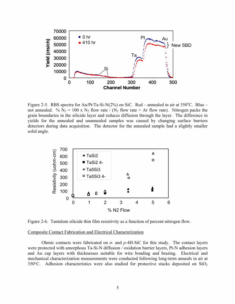
The effect of adding an Au layer above the Pt layer in the Pt/TaSi2 couple is shown in Figure 2-4. Gold is known to be a fast diffuser in many situations, and mixing is evident after 400hr anneals in air at 350oC anneals. The TaSi2 layer is likely polycrystalline as sputtered, so that Au diffusion along grain boundaries produces the mixing. However, when N2 is added to the Ar ambient in the sputter deposition system, one obtains the results shown in Figure 2-5. The addition of N2 has two effects – 1) grain size is reduced so that the TaSi2 layer is more nearly amorphous, and 2) nitrogen packs the remaining grain boundaries so that grain boundary diffusion is substantially reduced.
Channel Number
0 10000 20000 30000 40000 50000 60000 7000
0 100 200 300 400 500
0 hr 120 hr
Yiel
d (c
ts/c
h)
Pt
MoSi
4
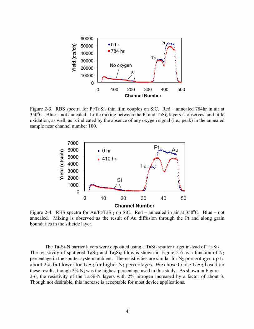
Figure 2-3. RBS spectra for Pt/TaSi2 thin film couples on SiC. Red – annealed 784hr in air at 350oC. Blue – not annealed. Little mixing between the Pt and TaSi2 layers is observes, and little oxidation, as well, as is indicated by the absence of any oxygen signal (i.e., peak) in the annealed sample near channel number 100.
Figure 2-4. RBS spectra for Au/Pt/TaSi2 on SiC. Red – annealed in air at 350oC. Blue – not annealed. Mixing is observed as the result of Au diffusion through the Pt and along grain boundaries in the silicide layer. The Ta-Si-N barrier layers were deposited using a TaSi2 sputter target instead of Ta3Si5. The resistivity of sputtered TaSi2 and Ta3Si5 films is shown in Figure 2-6 as a function of N2 percentage in the sputter system ambient. The resistivities are similar for N2 percentages up to about 2%, but lower for TaSi2 for higher N2 percentages. We chose to use TaSi2 based on these results, though 2% N2 was the highest percentage used in this study. As shown in Figure 2-6, the resistivity of the Ta-Si-N layers with 2% nitrogen increased by a factor of about 3. Though not desirable, this increase is acceptable for most device applications.
0 10000 20000 30000 40000 50000 60000
0 100 200 300 400 500 Channel Number
0 hr 784 hr
Pt
Ta
SiYiel
d (c
ts/c
h)
No oxygen
0 1000200030004000
5000
6000
7000
10
20
30
40
50 Channel Number
0 hr 410 hr
Pt Au
Si
Ta
Yiel
d (c
ts/c
h)
0
5
Figure 2-5. RBS spectra for Au/Pt/Ta-Si-N(2%) on SiC. Red – annealed in air at 350oC. Blue – not annealed. % N2 = 100 x N2 flow rate / (N2 flow rate + Ar flow rate). Nitrogen packs the grain boundaries in the silicide layer and reduces diffusion through the layer. The difference in yields for the annealed and unannealed samples was caused by changing surface barriers detectors during data acquisition. The detector for the annealed sample had a slightly smaller solid angle.
Figure 2-6. Tantalum silicide thin film resistivity as a function of percent nitrogen flow. Composite Contact Fabrication and Electrical Characterization Ohmic contacts were fabricated on n- and p-4H-SiC for this study. The contact layers were protected with amorphous Ta-Si-N diffusion / oxidation barrier layers, Pt-N adhesion layers and Au cap layers with thicknesses suitable for wire bonding and brazing. Electrical and mechanical characterization measurements were conducted following long-term anneals in air at 350°C. Adhesion characteristics were also studied for protective stacks deposited on SiO2
0100200300400500600700
0 1 2 3 4 5 6
% N2 Flow
Res
istiv
ity (u
ohm
-cm
)
TaSi2 TaSi2 4-Ta5Si3 Ta5Si3 4-
0 10000 20000 30000 40000 50000 60000 70000
0 100 200 300 400 500 Channel Number
Yiel
d (c
ts/c
h) 0 hr
410 hr New SBDPt Au
Ta
Si
0 10000 20000 30000 40000 50000 60000 70000
0 100 200 300 400 500 Channel Number
Yiel
d (c
ts/c
h) 0 hr
410 hr New SBDPt Au
Ta
Si

6
dielectric layers. The contact layer (or SiO2 layer) plus the protective stack make up the composite contact for either direct or indirect wire bonding as shown in Figure 2-1. Five millimeter by 5mm die from research grade 4H-SiC wafers with heavily implanted p+ epitaxial layers (Nimpl ~ 1e21cm-3
Al) or un-implanted n+ epilayers (Nd = 5e19cm-3) were cleaned using standard procedures, and linear transmission line (LTL) patterns for ohmic contacts were defined using photolithography. The alloy Al70Ti30 and Ni(7%V) were sputtered for contacts to p-SiC. Ni80Cr20 layers [and later Ni(7%V)] were deposited for n-SiC. Aluminum-titanium and Ni-Cr were annealed at 1000°C for 2min, and Ni(7%V) at 900°C for 1min – all in high vacuum (~ 1e-7Torr). The samples were then re-patterned by photolithography, and Ta-Si-N (~ 150nm) and Pt-N (~ 100nm) layers were sputtered without breaking vacuum from TaSi2 and Pt targets in Ar-N2 gas mixtures with 0-2% N2 flow [percentage = 100 x N2 flow(sccm)/(Ar + N2) flow(sccm)]. Finally, Au was sputtered as a cap layer for SiC die brazing and wire bonding. Early on, we encountered adhesion problems between Pt sputtered at room temperature and the Ta-Si-N layers. Platinum deposition at 250°C eliminated the problem, and deposition onto a hot substrate is now a standard part of our fabrication process. A thermosonic bonder was used to wedge-bond 10 mil (254 μm) diameter Au wire to thick Au cap layers of the composite contacts (see Figure 2-1). Bond pull and shear strengths were measured as a function anneal time in air at 350°C.
020406080
100120140
0 5 10 15 20
LTL Pad Spacing [micron]
Res
ista
nce
[ohm
]
p+ impl Al/Tin+ epi Ni/Crp+ impl Nip+ epi Ni
Figure 2-7. LTL pad to pad resistance as a function of pad spacing. Typical LTL (linear transmission line) plots of total contact-to-contact resistance as a function of contact spacing are shown in Figure 2-7 for Ni contacts on p+ implanted epitaxial material and Ni80Cr20 contacts on n+ epitaxial material. The specific contact resistance rc and the SiC sheet resistance Rsh were obtained using these plots and the equation

7
W is the width of the contacts in the LTL pattern, and L is the inter-contact spacing [2.9]. The specific contact resistances and sheet resistances with and without the protective stacks (Ta-Si-N / Pt-N / Au) were not significantly different. Figure 2-8 shows the plots of the specific contact resistance and SiC sheet resistance as a function of anneal time for 2% nitrogen content in the stacks. Also included are plots for Ni and AlTi contacts to p-4H-SiC that were fabricated without nitrogen in the barrier layer (open symbols). Following an initial rise very early in the annealing process, the specific contact resistance for the n-ohmic NiCr contact remains stable and then decreases for long anneal times. However, the p-ohmic AlTi contact without nitrogen in the Ta-Si barrier layer is characterized by a slow but steady rise in specific contact resistance. This sample is currently awaiting AES (Auger Electron Spectroscopy) analysis to determine whether oxidation might be the problem. Using AES rather that RBS, we will be able to look at the TLM patterns themselves, and we will have better sensitivity to light elements like oxygen. Ohmic contacts on n+-epilayers were fabricated with 80-20 weight percent Ni-Cr. This alloy forms a nickel silicide ohmic contact, with the advantage that, for thin NiCr layers [2.10], Cr improves adhesion between the nickel silicide contact layer and an Au over-layer, in the absence of other layers such as Pt or Ta-Si-N. With these adhesion / barrier layers in the composite stack, Ni can be used for the n-ohmic contacts. Indeed, Ni is the most commonly used metal for n-ohmic contacts to SiC. Thus for suitably high doping concentrations, Ni serves as a good ohmic contact metal for both n- and p-4H-SiC. An Al alloy such as AlTi or AlNi is
Figure 2-8. Sheet resistance (left) and specific contact resistance (right) for composite ohmic contacts as a function of anneal time in air at 350oC. Ni80Cr20 was used to form ohmic contacts to n-4H-epilayers (5x1019cm-3). Ni(7%) and Al70Ti30 were used for implanted p-4H-SiC (Al implant = 1x1021cm-3). normally used for ohmic contacts to moderately doped p-SiC (< 5x1018cm-3) [2.11]. This requirement is likely the result of the way the contact layer forms in the presence of Al [2.12].
0.0E+00
1.0E-04
2.0E-04
3.0E-04
4.0E-04
5.0E-04
6.0E-04
0 2000 4000 6000 8000
Time (hr)
Spec
. Con
tact
Res
. (oh
m-c
m2) 0%N2 Ni 2%N2 Ni
0%N2 Al-Ti 2%N2 Al-Ti2%N2 Ni-Cr
0.0E+00
2.0E+02
4.0E+02
6.0E+02
8.0E+02
1.0E+03
1.2E+03
1.4E+03
0 2000 4000 6000 8000
Time (hr)
Shee
t Res
. (oh
m/s
q)
0%N2 Ni 0%N2 Al-Ti 2%N2 Ni-Cr2%N2 Ni 2%N2 Al-Ti
.2W
LRW
RrR shshc
T +=

8
Mechanical Characterization Adhesion within the protective stack and adhesion of the stack to SiO2 (indirect bonding) and to the ohmic contacts (direct bonding) are necessary for robust packaging. Indications of adhesion problems were first noticed following the direct brazing of SiC / SiO2 / Ta-Si-N / Pt-N / Au samples to Cu-plated ceramic die carriers. Adhesion was degraded significantly during thermal aging in air. Rutherford backscattering analysis of a sheared sample showed that separation occurred at the interface between Ta-Si-N and Pt in the protective stack. Adhesion at this interface was greatly improved by sputtering Pt onto SiC / SiO2 / Ta-Si-N at 250°C. Bond pull and bond shear testing (Figure 2-9) were carried out on two structures: SiC / SiO2 / Ta-Si-N / Pt-N / Au and SiC / Ni2Si (ohmic) / Ta-Si-N / Pt-N / Au. Test results shown in Figire 2-10 indicate that the protective stacks with hot Pt have held up very well. One hundred percent of the time, we observed that the Au wires broke during the pull tests, and for the bond shear tests, the separation of the wire bonds from the samples occurred above the Au cap layers. Early on, wire bond pull and shear test results were not as good for hot Pt stacks deposited directly on annealed nickel contacts. Many bonds failed at the interface between the ohmic contact and the Ta-Si-N layer. These failures were attributed to residual carbon contamination on the surface of the nickel silicide layer following the ohmic contact anneal. Auger electron spectra confirmed the presence of surface nickel and carbon in the ratio of about 1:2 (Ni:C) for annealed contacts. For contact layers subsequently cleaned with an Ar ion beam (1keV, 5 minutes), the Ni:C ratio increased to about 5:4, and significant improvement in the adhesion of the Ta-Si-N layers to the contact layers was observed. The direct wire bond results in Figure 2-10 were been obtained using ion-cleaned nickel silicide ohmic contact layers.
Figure 2-9. Arrangement for wire bond pull and shear testing.
600μ
400μ
Stack SiO2
Pull Shear
SiC

9
0200400600800
10001200140016001800
0 1000 2000 3000 4000 5000 6000
Time (hr)
Pull/
Shea
r Str
engt
h (g
)
pull SiO2shear SiO2pull Ni p-ohmicshear Ni p-ohmic
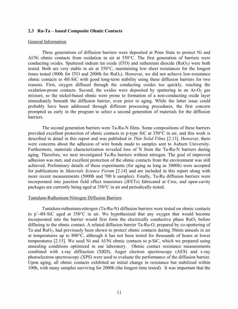
Figure 2-10. Wire bond pull and shear results for Au/ Pt (250oC) / Ta-Si-N stacks on SiO2 and nickel silicide ohmic contact layers. The ohmic contact layers were cleaned of excess carbon with a low energy Ar ion beam. Rutherford backscattering spectra are show in Figures 2- 11 and 2-12 for composite p-ohmic Ni contacts and Au/Pt/Ta-Si-N(2%) stacks on SiO2 respectively. Variations in signal height (i.e., differences in yield) are caused by variations in beam current integration which determines the total number of alpha particles incident on the sample. For both figures, signal widths from the components of in the stacks do not change significantly during long-term aging in air at 350oC – an indication of excellent long-term stability. Figure 2-11. RBS spectra for composite Ni ohmic contacts to p-4H-SiC. Variations in peak height are due to variations in beam current integration. Significant variations in the elemental signal widths are not observed. This indicates that the composite contact remains stable during long-term aging in air at 350oC.
0.0E+00
1.0E+04
2.0E+04
3.0E+04
4.0E+04
5.0E+04
6.0E+04
0 100 200 300 400 500Channel Number
Yiel
d (c
ts/c
h)
24hr1500hr4000hr7000hr
Au Pt
Ta
NiSi
10
Figure 2-12. RBS spectra for composite Au/Pt/Ta-Si-N(2%) protective stacks on SiO2. Variations in peak height are due to variations in beam current integration. Signal widths from the components in the stack do not vary significantly over time and that the stack remains stable after long-term aging in air at 350oC. Note also that the oxygen signal near channel number 75 does not increase significantly after 7000hr. As mentioned previously, we have observed degradation in the electrical performance of p-ohmic AlTi contacts fabricated using protective stacks (Au/Pt/Ta-Si) without nitrogen. These samples are currently awaiting AES analysis to determine whether changes in physical characteristics such as oxidation or inter-diffusion can be correlated with the observed changes in electrical performance. Compared to RBS, AES depth profiling will provide a clearer picture of how oxygen is affecting the composite contact. We will supply the AES spectra as soon as we have them – either in the final version of this report or as and addendum to it. Conclusions Nickel and NiCr make excellent ohmic contacts to n-4H-SiC, and Ni makes a very good ohmic contact to p-4H-SiC for doping concentrations above 2-3x1019cm-3. Below these concentration levels, Al is often added (e.g., Al Ti or NiAl) in order to form p-ohmic contacts with acceptably low specific contact resistances. For all cases, the protective stack Au/Pt-N/Ta-Si-N with around 2% nitrogen content was found to be very resistant to oxidation and inter-diffusion when used with Ni, NiCr and AlTi for composite contacts to SiC. The electrical characteristics of protected contacts did not degrade after aging for 7000hr in air at 350oC. Platinum deposition at 250oC complicates the fabrication of the protective stack to some extent, but significantly improves adhesion within the stack. Excellent results for wire bond pull and shear testing were obtained with hot Pt stacks deposited on SiO2 and on Ni ohmic contacts that were pre-cleaned with a low energy Ar ion beam to remove excess carbon liberated during the ohmic contact anneal.
0.0E+00
1.0E+04
2.0E+04
3.0E+04
4.0E+04
5.0E+04
6.0E+04
0 100 200 300 400 500 Channel Number
24hr 1500hr 4000hr 7000hr
O
Au
Si
Ta
Pt
Yie
ld
11
2.3 Ru-Ta – based Composite Ohmic Contacts General Information Three generations of diffusion barriers were deposited at Penn State to protect Ni and Al/Ni ohmic contacts from oxidation in air at 350°C. The first generation of barriers were conducting oxides. Sputtered indium tin oxide (ITO) and ruthenium dioxide (RuO2) were both tested. Both are very stable in air at 350°C, maintaining low sheet resistances for the longest times tested (900h for ITO and 2000h for RuO2). However, we did not achieve low-resistance ohmic contacts to 4H-SiC with good long-term stability using these diffusion barriers for two reasons. First, oxygen diffused through the conducting oxides too quickly, reaching the oxidation-prone contacts. Second, the oxides were deposited by sputtering in an Ar-O2 gas mixture, so the nickel-based ohmic were prone to formation of a non-conducting oxide layer immediately beneath the diffusion barrier, even prior to aging. While the latter issue could probably have been addressed through different processing procedures, the first concern prompted us early in the program to select a second generation of materials for the diffusion barriers. The second generation barriers were Ta-Ru-N films. Some compositions of these barriers provided excellent protection of ohmic contacts to p-type SiC at 350°C in air, and this work is described in detail in this report and was published in Thin Solid Films [2.13]. However, there were concerns about the adhesion of wire bonds made to samples sent to Auburn University. Furthermore, materials characterization revealed loss of N from the Ta-Ru-N barriers during aging. Therefore, we next investigated Ta-Ru barriers without nitrogen. The goal of improved adhesion was met, and excellent protection of the ohmic contacts from the environment was still achieved. Preliminary details of these experiments (for aging as long as 3000h) were accepted for publications in Materials Science Forum [2.14] and are included in this report along with more recent measurements (5000h and 700 h samples). Finally, Ta-Ru diffusion barriers were incorporated into junction field effect transistors (JFETs) fabricated at Cree, and open-cavity packages are currently being aged at 350°C in air and periodically tested. Tantalum-Ruthenium-Nitrogen Diffusion Barriers Tantalum-ruthenium-nitrogen (Ta-Ru-N) diffusion barriers were tested on ohmic contacts to p+-4H-SiC aged at 350°C in air. We hypothesized that any oxygen that would become incorporated into the barrier would first form the electrically conductive phase RuO2 before diffusing to the ohmic contact. A related diffusion barrier Ta-Ru-O, prepared by co-sputtering of Ta and RuO2, had previously been shown to protect ohmic contacts during 30min anneals in air at temperatures up to 800°C, although it has not been tested for thousands of hours at lower temperatures [2.15]. We used Ni and Al/Ni ohmic contacts to p-SiC, which we prepared using annealing conditions optimized in our laboratory. Ohmic contact resistance measurements combined with x-ray diffraction (XRD), Auger electron spectroscopy (AES) and x-ray photoelectron spectroscopy (XPS) were used to evaluate the performance of the diffusion barrier. Upon aging, all ohmic contacts exhibited an initial change in resistance but stabilized within 100h, with many samples surviving for 2000h (the longest time tested). It was important that the
12
Ru:Ta in the barriers be sufficiently high to obtain a long-lived barrier in air. Specific contact resistances as low as 3 x 10⁻⁵ohm-cm2 were maintained after 2000h of aging. A research grade n-type 4H SiC wafer (ND = 3.9 x 1017cm-3) with a SiC epilayer (NA = 7.5 x 1018cm-3) beneath a SiC epilayer implanted with a target acceptor concentration of 1 x 1021cm-3 was provided by Cree, Inc. Samples were degreased using a 5 min acetone soak and 5min methanol soak, followed by a deionized (DI) water rinse and N2 gas to dry the samples. Patterning of the contacts was performed using photolithography after degreasing to prepare the samples for liftoff of the metallization. The native oxide on SiC was next removed with a 2min dip in buffered oxide etch. The samples were then rinsed in DI water, blown dry with N2, and immediately loaded into the deposition chamber. Ni (100nm) contacts or Al/Ni contacts (15nm of Al followed by 50nm of Ni) were deposited by DC magnetron sputtering. It should be noted that slightly different procedures were next required, depending on whether Ni or Al/Ni was used. The barrier layers exhibited poor adhesion to the Ni contacts if they were annealed before the barrier was deposited, so annealing of the barrier along with the ohmic contact was required. On the other hand, the Al/Ni contact required annealing prior to deposition of the barrier, otherwise a high specific contact resistance of 2 x 10⁻³ohm-cm2 resulted, and further study was limited due to the high specific contact resistances. In this case, it was necessary to perform photolithography a second time for liftoff of the barrier layer. Interestingly, the barrier layers still adhered well to the Al/Ni contacts after they were annealed. The diffusion barriers were deposited to a thickness of 200nm using reactive DC co-sputtering of Ru and Ta metallic targets in N2-Ar at 6 mTorr working pressure and a base pressure of 2 x 10⁻⁷ Torr. The sputtering gases were Ar (99.999%) and N2 (99.999%). Three compositions of the barrier were fabricated by varying the N2:Ar ratio, the placement of the samples within the chamber, and the powers of the Ta and Ru sputter heads. The compositions of the barrier are labeled Ru-rich, Ta-rich, and for the barrier with roughly equal Ta and Ru concentrations, 50-50. The Ru-rich and 50-50 barriers were sputter-deposited with a 1:1 N2:Ar ratio, while the Ta-rich barrier was sputter-deposited with a 1:3 N2:Ar ratio. The Ta was sputtered at a power level such that a nitride formed on the target during sputtering. For the Ru-rich and 50-50 compositions, the power of the Ru and Ta sputter heads were 60 and 170W, respectively, and the powers for the Ta-rich composition were 40 and 160W, respectively. After depositing the barrier on the Ni contacts, the samples were patterned by photolithography a final time. For all samples a Pt/Sn/Au (100nm/25nm/200nm) cap was then sputtered for future packaging experiments. The final contact metallization consisted of Ni (100 nm) / Ta-Ru-N (200nm) / Pt (100nm) / Sn (25nm) / Au (200nm) for the samples with Ni ohmic contacts and Al (15nm) / Ni (100nm) / Ta-Ru-N (200nm) / Pt (100nm) / Sn (25nm) / Au (200 m) for the Al/Ni samples. Specific contact resistances were extracted using the circular transfer length method (CTLM) with 80 micron diameter contacts separated by gap spacings of 4, 8, 14, 20, 30, 50 and 75 micron from a broad area contact. Broad area samples with identical processing to the patterned contact samples were prepared for depth profile analysis. Depth profiles of the barrier
13
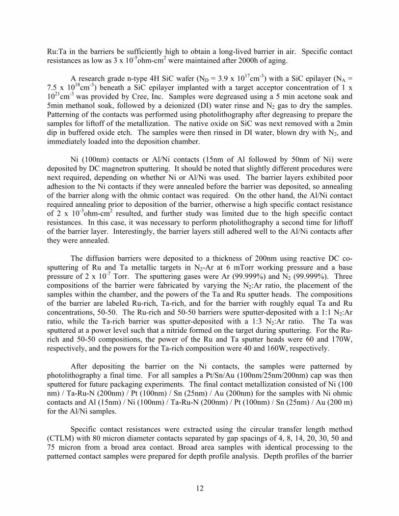
layers were obtained using AES and XPS. Auger electron spectroscopy was performed using a PHI 670 with 10nA beam current at 10kV. The XPS was performed using a Kratos Ultra with a monochromatic Al K x-ray source. The crystallinity of the barrier layers deposited directly on SiC was monitored using glancing angle x-ray diffraction performed on a Phillips XRD using a Cu K x-ray source with a 1.2° angle of incidence. Samples for x-ray diffraction were aged in evacuated quartz tubes and in air at 350°C. A plot summarizing the samples with Ni contacts is shown in Figure 2.13. Figures 2.13 and 2.14 include the measurements for 2 samples of each type of barrier, each with multiple sets of CTLM test structures. The as-prepared Ni contacts showed excellent reproducibility. All samples had initial shifts in specific contact resistance but stabilized after 100 h in air at 350 °C. The Ru-rich composition showed the most promise for a stable oxygen diffusion barrier for Ni ohmic contacts. The average specific contact resistance of the Ni contacts beneath the Ru-rich barriers improved from 6 x 10⁻⁵ohm-cm2 to 3 x 10⁻⁵ohm-cm2 after 100h and changed only slightly after 2000h, exhibiting an average specific contact resistance of 5 x 10⁻⁵ohm-cm2. Contacts beneath the 50-50 and Ta-rich barriers showed an initial increase in specific contact resistance and stabilized after 100h. A plot summarizing the samples with Al/Ni contacts is shown in Figure 2-14. The Al/Ni contacts exhibited larger variations in the as-prepared specific contact resistances, which varied from 2 x 10⁻⁵ohm-cm2 to 2 x 10⁻⁴ohm-cm2. However, the Al/Ni contacts had a lower specific contact resistance on average compared to the Ni samples. The contacts under the Ta-rich barrier were the only contacts to show degradation in specific contact resistance for times less than 100 h. The Al/Ni contacts under the Ru-rich barrier had a specific contact resistance as low as 2 x 10⁻⁵ohm-cm2 in the as-prepared condition and after 100h, and after 2000 h of aging the specific contact resistance was as low as 3 x 10⁻⁵ohm-cm2. The Ru-rich and 50-50 barriers showed the best combination of stability and low specific contact resistance for the Al/Ni contacts.
Figure 2-13. Specific contact resistances of Ni ohmic contacts beneath different barriers aged at 350°C in air.

14
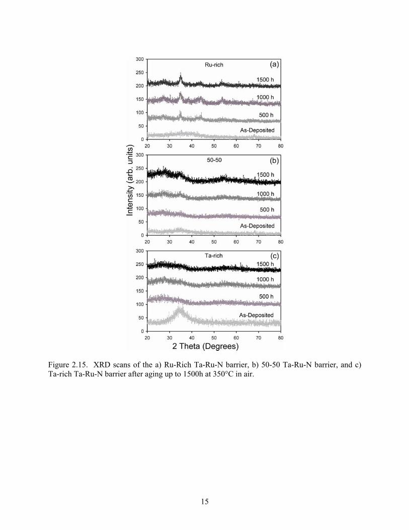
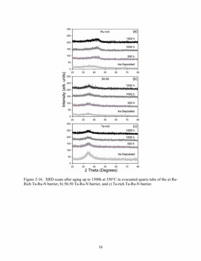
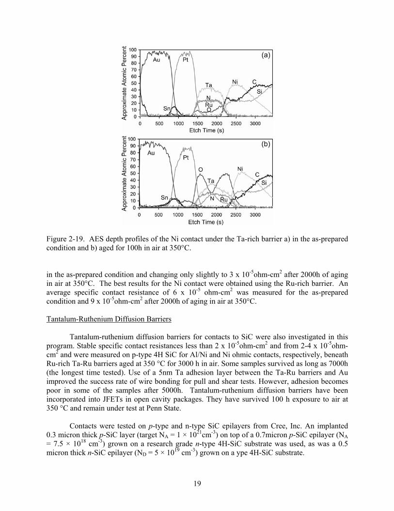
Figure 2-14. Specific contact resistances of Al/Ni ohmic contacts beneath different barriers aged at 350°C in air. To determine the degree of crystallinity of the Ta-Ru-N diffusion barriers, glancing angle x-ray diffraction was used. Thin film barriers without the other metallization layers were deposited on SiC and subsequently aged in air and evacuated quartz tubes. All barriers displayed amorphous x-ray diffraction patterns in the as-deposited condition, as shown in Figures 2-15 and 2.16. The x-ray diffraction scans of the Ru-rich composition in Figure 2-15 displayed signs of crystallization after 500 h in air. The 50-50 barrier displayed signs of crystallization after 1500h in air, while the Ta-rich barrier remained amorphous for up to 1500 h in air. Nevertheless, the ohmic contacts did not show evidence of degradation (increase in contact resistance) beneath the Ru-rich barriers, despite the early onset of crystallization of layers aged in air with no Pt/Sn/Au cap. On the other hand, all of the x-ray diffraction plots in Figure 2-16 show that the Ta-Ru-N barriers remain amorphous for up to 1500 h when held in evacuated quartz tubes instead of air. The crystallized phase of the Ru-rich and 50-50 barriers aged in air could not be identified as a known Ru or Ta oxide or nitride. An AES depth profile of the Ni contact under the Ru-rich barrier in the as-prepared condition is shown in Figure 2-17a. It has been shown that upon formation of nickel silicide in annealed ohmic contacts to SiC, there is segregation of carbon as graphitically-bonded inclusions [2.16]. Similarly, there is evidence for the formation of a nickel silicide along with a carbon rich layer in the AES depth profiles of the as-deposited and annealed nickel contacts shown in Figures 2.17a and 2-17b. However, there is minimal reaction of the barrier layer with the contact, even though they were annealed together.
15
Figure 2.15. XRD scans of the a) Ru-Rich Ta-Ru-N barrier, b) 50-50 Ta-Ru-N barrier, and c) Ta-rich Ta-Ru-N barrier after aging up to 1500h at 350°C in air.
16
Figure 2-16. XRD scans after aging up to 1500h at 350°C in evacuated quartz tube of the a) Ru-Rich Ta-Ru-N barrier, b) 50-50 Ta-Ru-N barrier, and c) Ta-rich Ta-Ru-N barrier.

17
Figure 2-17. AES depth profiles of the Ni contact under the Ru-rich barrier a) in the as-prepared condition and b) aged for 2000h in air at 350°C. After aging of the Ru-rich barrier for 2000h at 350°C, it is evident in the AES depth profile in Figure 2-17b that there is a large loss of nitrogen from the barrier combined with an increase in oxygen. The O:Ru ratio in the Ru-rich barrier sample is approximately 0.2:1 as-prepared and 1.3:1 after aging for 2000h at 350°C. A near coincidence of the Auger energy transitions for the C KLL (272eV) and Ru MNN (273eV) made determination of the C concentration in the AES depth profiles more challenging, and data collected in this energy range were deconvoluted. To provide a check on the accuracy of the deconvolution procedure, an XPS depth profile of one as-prepared sample was collected along with an AES depth profile, and the profiles obtained by the two different methods matched each other closely. The XPS profile is shown in Figure 2-18a for a sample with the 50-50 barrier above an Al/Ni contact in the as-prepared condition. Upon annealing the Al/Ni contacts (as-prepared condition), the Al and Ni redistribute, and the Ni reacts with the SiC. After aging for 2000h, the Ru-rich barrier shows a greater loss of nitrogen than the 50-50 barrier shown in the XPS depth profiles of the as-prepared sample in Figure 2-18a and the sample aged for 2000h at 350°C in Figure 2-18b. This is likely due to the lack of a stable ruthenium nitride, as no report of any ruthenium nitrides could be found in the literature. Even with this loss of nitrogen, the Ru-rich barrier still protected the underlying contacts, indicating that the nitrogen content in the barrier may not be necessary.
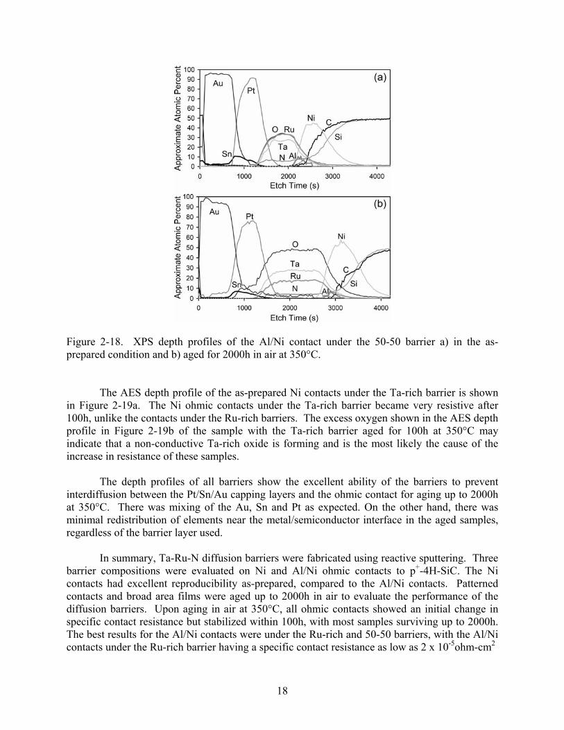
18
Figure 2-18. XPS depth profiles of the Al/Ni contact under the 50-50 barrier a) in the as-prepared condition and b) aged for 2000h in air at 350°C. The AES depth profile of the as-prepared Ni contacts under the Ta-rich barrier is shown in Figure 2-19a. The Ni ohmic contacts under the Ta-rich barrier became very resistive after 100h, unlike the contacts under the Ru-rich barriers. The excess oxygen shown in the AES depth profile in Figure 2-19b of the sample with the Ta-rich barrier aged for 100h at 350°C may indicate that a non-conductive Ta-rich oxide is forming and is the most likely the cause of the increase in resistance of these samples. The depth profiles of all barriers show the excellent ability of the barriers to prevent interdiffusion between the Pt/Sn/Au capping layers and the ohmic contact for aging up to 2000h at 350°C. There was mixing of the Au, Sn and Pt as expected. On the other hand, there was minimal redistribution of elements near the metal/semiconductor interface in the aged samples, regardless of the barrier layer used. In summary, Ta-Ru-N diffusion barriers were fabricated using reactive sputtering. Three barrier compositions were evaluated on Ni and Al/Ni ohmic contacts to p+-4H-SiC. The Ni contacts had excellent reproducibility as-prepared, compared to the Al/Ni contacts. Patterned contacts and broad area films were aged up to 2000h in air to evaluate the performance of the diffusion barriers. Upon aging in air at 350°C, all ohmic contacts showed an initial change in specific contact resistance but stabilized within 100h, with most samples surviving up to 2000h. The best results for the Al/Ni contacts were under the Ru-rich and 50-50 barriers, with the Al/Ni contacts under the Ru-rich barrier having a specific contact resistance as low as 2 x 10⁻⁵ohm-cm2
19
Figure 2-19. AES depth profiles of the Ni contact under the Ta-rich barrier a) in the as-prepared condition and b) aged for 100h in air at 350°C. in the as-prepared condition and changing only slightly to 3 x 10⁻⁵ohm-cm2 after 2000h of aging in air at 350°C. The best results for the Ni contact were obtained using the Ru-rich barrier. An average specific contact resistance of 6 x 10⁻⁵ ohm-cm2 was measured for the as-prepared condition and 9 x 10⁻⁵ohm-cm2 after 2000h of aging in air at 350°C. Tantalum-Ruthenium Diffusion Barriers Tantalum-ruthenium diffusion barriers for contacts to SiC were also investigated in this program. Stable specific contact resistances less than 2 x 10⁻⁵ohm-cm2 and from 2-4 x 10⁻⁵ohm-cm2 and were measured on p-type 4H SiC for Al/Ni and Ni ohmic contacts, respectively, beneath Ru-rich Ta-Ru barriers aged at 350 °C for 3000 h in air. Some samples survived as long as 7000h (the longest time tested). Use of a 5nm Ta adhesion layer between the Ta-Ru barriers and Au improved the success rate of wire bonding for pull and shear tests. However, adhesion becomes poor in some of the samples after 5000h. Tantalum-ruthenium diffusion barriers have been incorporated into JFETs in open cavity packages. They have survived 100 h exposure to air at 350 °C and remain under test at Penn State. Contacts were tested on p-type and n-type SiC epilayers from Cree, Inc. An implanted 0.3 micron thick p-SiC layer (target NA = 1 × 1021cm-3) on top of a 0.7micron p-SiC epilayer (NA = 7.5 × 1018 cm-3) grown on a research grade n-type 4H-SiC substrate was used, as was a 0.5 micron thick n-SiC epilayer (ND = 5 × 1019 cm-3) grown on a ype 4H-SiC substrate.
20
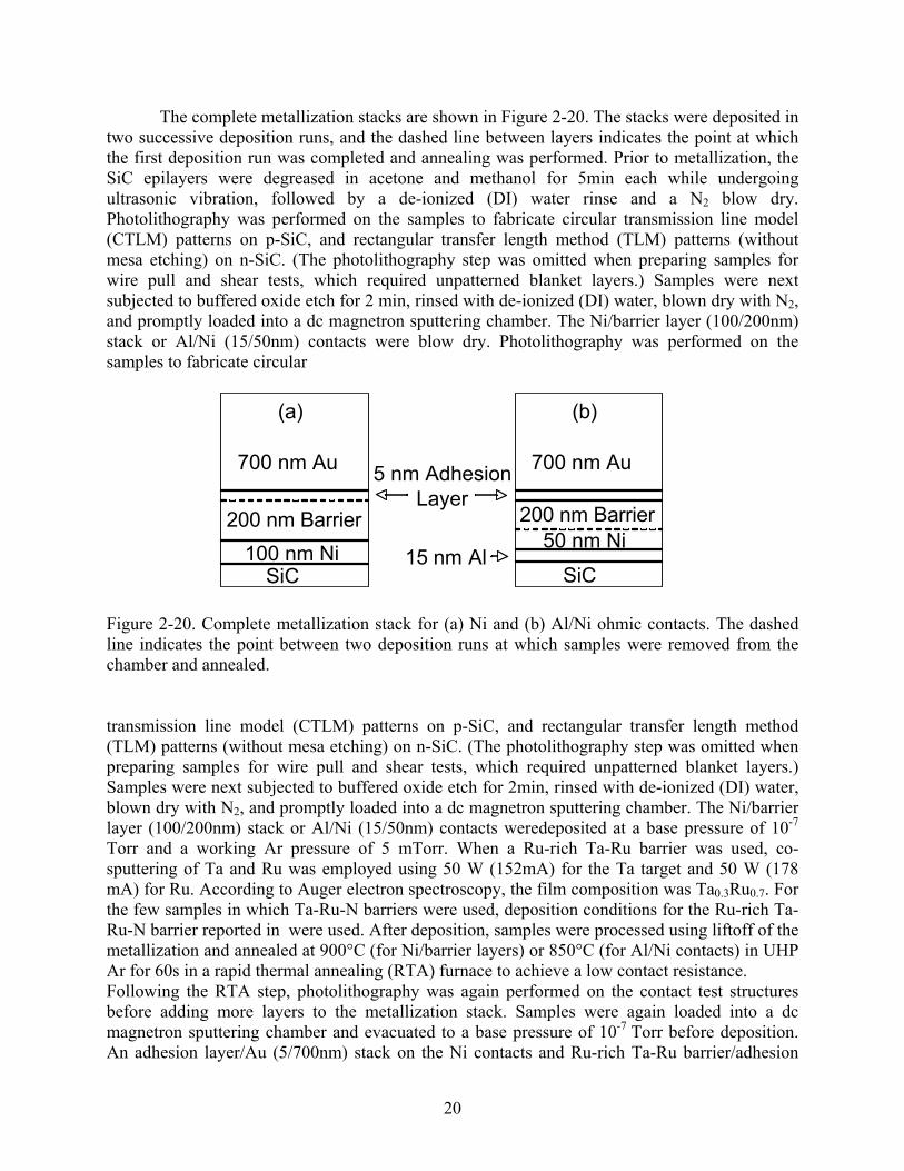
The complete metallization stacks are shown in Figure 2-20. The stacks were deposited in two successive deposition runs, and the dashed line between layers indicates the point at which the first deposition run was completed and annealing was performed. Prior to metallization, the SiC epilayers were degreased in acetone and methanol for 5min each while undergoing ultrasonic vibration, followed by a de-ionized (DI) water rinse and a N2 blow dry. Photolithography was performed on the samples to fabricate circular transmission line model (CTLM) patterns on p-SiC, and rectangular transfer length method (TLM) patterns (without mesa etching) on n-SiC. (The photolithography step was omitted when preparing samples for wire pull and shear tests, which required unpatterned blanket layers.) Samples were next subjected to buffered oxide etch for 2 min, rinsed with de-ionized (DI) water, blown dry with N2, and promptly loaded into a dc magnetron sputtering chamber. The Ni/barrier layer (100/200nm) stack or Al/Ni (15/50nm) contacts were blow dry. Photolithography was performed on the samples to fabricate circular
SiC100 nm Ni
200 nm Barrier
5 nm AdhesionLayer
700 nm Au
(a)
SiC15 nm Al
700 nm Au
(b)
200 nm Barrier50 nm Ni
Figure 2-20. Complete metallization stack for (a) Ni and (b) Al/Ni ohmic contacts. The dashed line indicates the point between two deposition runs at which samples were removed from the chamber and annealed. transmission line model (CTLM) patterns on p-SiC, and rectangular transfer length method (TLM) patterns (without mesa etching) on n-SiC. (The photolithography step was omitted when preparing samples for wire pull and shear tests, which required unpatterned blanket layers.) Samples were next subjected to buffered oxide etch for 2min, rinsed with de-ionized (DI) water, blown dry with N2, and promptly loaded into a dc magnetron sputtering chamber. The Ni/barrier layer (100/200nm) stack or Al/Ni (15/50nm) contacts weredeposited at a base pressure of 10-7 Torr and a working Ar pressure of 5 mTorr. When a Ru-rich Ta-Ru barrier was used, co-sputtering of Ta and Ru was employed using 50 W (152mA) for the Ta target and 50 W (178 mA) for Ru. According to Auger electron spectroscopy, the film composition was Ta0.3Ru0.7. For the few samples in which Ta-Ru-N barriers were used, deposition conditions for the Ru-rich Ta-Ru-N barrier reported in were used. After deposition, samples were processed using liftoff of the metallization and annealed at 900°C (for Ni/barrier layers) or 850°C (for Al/Ni contacts) in UHP Ar for 60s in a rapid thermal annealing (RTA) furnace to achieve a low contact resistance. Following the RTA step, photolithography was again performed on the contact test structures before adding more layers to the metallization stack. Samples were again loaded into a dc magnetron sputtering chamber and evacuated to a base pressure of 10-7 Torr before deposition. An adhesion layer/Au (5/700nm) stack on the Ni contacts and Ru-rich Ta-Ru barrier/adhesion
21
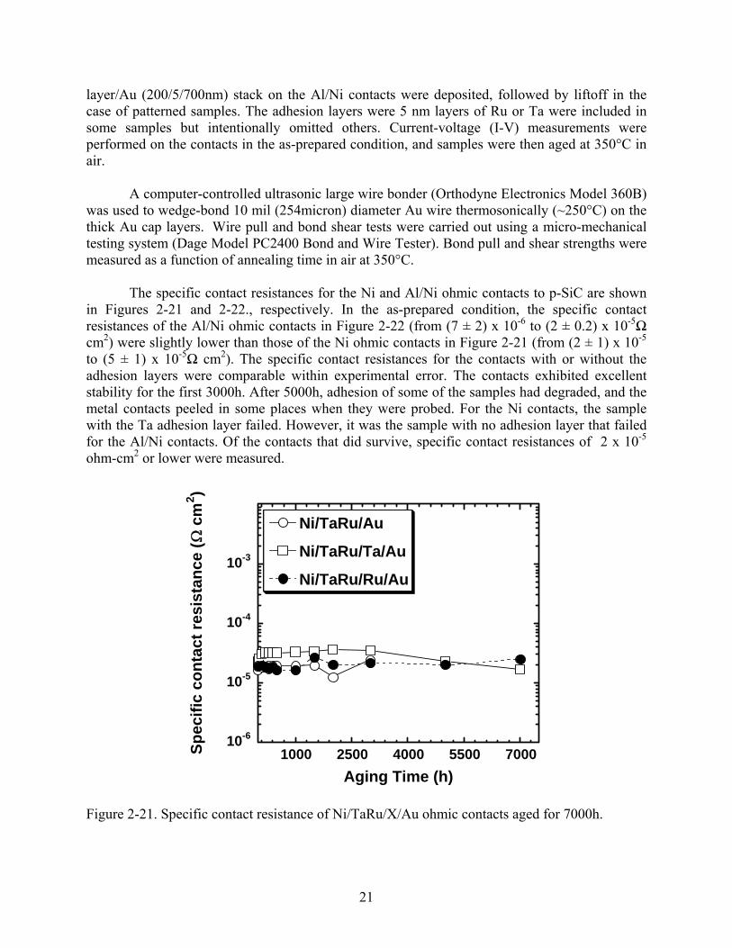
layer/Au (200/5/700nm) stack on the Al/Ni contacts were deposited, followed by liftoff in the case of patterned samples. The adhesion layers were 5 nm layers of Ru or Ta were included in some samples but intentionally omitted others. Current-voltage (I-V) measurements were performed on the contacts in the as-prepared condition, and samples were then aged at 350°C in air. A computer-controlled ultrasonic large wire bonder (Orthodyne Electronics Model 360B) was used to wedge-bond 10 mil (254micron) diameter Au wire thermosonically (~250°C) on the thick Au cap layers. Wire pull and bond shear tests were carried out using a micro-mechanical testing system (Dage Model PC2400 Bond and Wire Tester). Bond pull and shear strengths were measured as a function of annealing time in air at 350°C. The specific contact resistances for the Ni and Al/Ni ohmic contacts to p-SiC are shown in Figures 2-21 and 2-22., respectively. In the as-prepared condition, the specific contact resistances of the Al/Ni ohmic contacts in Figure 2-22 (from (7 ± 2) x 10-6 to (2 ± 0.2) x 10-5Ω cm2) were slightly lower than those of the Ni ohmic contacts in Figure 2-21 (from (2 ± 1) x 10-5 to (5 ± 1) x 10-5Ω cm2). The specific contact resistances for the contacts with or without the adhesion layers were comparable within experimental error. The contacts exhibited excellent stability for the first 3000h. After 5000h, adhesion of some of the samples had degraded, and the metal contacts peeled in some places when they were probed. For the Ni contacts, the sample with the Ta adhesion layer failed. However, it was the sample with no adhesion layer that failed for the Al/Ni contacts. Of the contacts that did survive, specific contact resistances of 2 x 10⁻⁵ ohm-cm2 or lower were measured.
10-6
10-5
10-4
10-3
1000 2500 4000 5500 7000
Ni/TaRu/Au
Ni/TaRu/Ta/Au
Ni/TaRu/Ru/Au
Spec
ific
cont
act r
esis
tanc
e (Ω
cm
2 )
Aging Time (h)
Figure 2-21. Specific contact resistance of Ni/TaRu/X/Au ohmic contacts aged for 7000h.

22
10-6
10-5
10-4
10-3
1000 2500 4000 5500 7000
Al/Ni/TaRu/Au
Al/Ni/TaRu/Ta/Au
Al/Ni/TaRu/Ru/AuSp
ecifi
c co
ntac
t res
ista
nce
(Ω c
m2 )
Aging Time (h)
Figure 2.22. Specific contact resistance of Al/Ni/TaRu/X/Au contacts aged for 7000h. The Al/Ni contacts we prepared were not ohmic on n-SiC, but aging of low-resistance Ni ohmic contacts with Ru-rich Ta-Ru barriers on n-SiC was performed. There was no increase in resistance after samples were aged at 350°C in air for 1000h (the longest time tested), indicating that the barriers are also provide effective protection of the underlying Ni ohmic contacts to n-SiC. Pull and shear tests of were next performed to investigate the adhesion of the previously reported metallizations with Ta-Ru-N barriers [2.13] and the new Ta-Ru barrier. Metallization stacks consisting of Ta-Ru-N/adhesion layer (Ru or Ta)/Au (200/5/700nm) on top of Ni and Al/Ni ohmic contacts were first tested. Many of these metallizations peeled during the wire bonding process, and there was poor adhesion of layers to the Ta-Ru-N barrier. On the other hand, wire bonding to metallization stacks with the Ru-rich Ta-Ru barriers was performed successfully on most of the samples. Pull and shear tests were then conducted. As shown in Figures 2-23 and 2-24, annealing of the metallization stacks at 350°C in air for 2000h did not greatly influence the pull and shear strengths. The highest pull and shear strengths were obtained for the Al/Ni/Ru-rich barrier/Ta/Au metallization stacks, in which the pull and shear strength were 840g and 1710g, respectively, for the as-prepared condition. These values changed only slightly to 810g for the pull strength and 1890g for the shear strength for metallization stacks aged at 350°C in air for 2000 h. However, reduced strength of samples with Ta adhesion layers was noted after 5000h. The Ni/TaRu/Ta/Au ohmic contact pads also peeled during probing after aging for 5000h.

23
0
500
1000
1500
2000
2500
3000
0 1000 2000 3000 4000 5000
Ni/TaRu/Ta/Au
Al/Ni/TaRu/Au
Al/Ni/TaRu/Ta/AuPu
ll St
reng
th (g
)
Aging Time (h) Figure 2.23. Pull tests results on metallizations stacks aged at 350°C in air.
0
500
1000
1500
2000
2500
3000
0 1000 2000 3000 4000 5000
Ni/TaRu/Ta/Au
Al/Ni/TaRu/Au
Al/Ni/TaRu/Ta/Au
Shea
r Str
engt
h (g
)
Aging Time (h)
Figure 2-24. Shear test results on metallization stacks aged at 350 °C in air.
24
Pull and shear tests were also conducted on metallization stacks deposited on SiO2, revealing good adhesion as prepared: Au/TaRu/SiO2/SiC, Au/Ta/TaRu/SiO2/SiC, and Au/Ru/TaRu/SiO2/SiC. Only two of these samples were aged. The Au/TaRu/SiO2/SiC and Au/Ta/TaRu/SiO2/SiC both exhibited good adhesion even after 5000h at 350°C in air. In summary, Ta-Ru diffusion barriers with 70% Ru effectively serve as diffusion barriers for Ni and Al/Ni ohmic contacts to p-SiC aged in air at 350°C for 3000h, with some samples surviving as long as 7000h (the longest time tested). Degraded adhesion leads to the eventual failure of some of the samples aged for 5000h, and poor adhesion is the dominant failure mode of the samples that do not survive. However, metallization stacks on SiO2 all survived pull and shear tests after exposure to air at 350°C for 5000h. Conclusions Two families of ruthenium-bearing diffusion barriers were examined in-depth. Tantalum-ruthenium-nitrogen barriers were prepared using reactive sputtering in Ar and N2 gas. Three Ta-Ru-N compositions were evaluated on Ni and Al/Ni ohmic contacts to p+-4H-SiC, and patterned contacts and broad area films were aged up to 2000h in air to evaluate the performance of the diffusion barriers. Upon aging in air at 350°C, all ohmic contacts showed an initial change in specific contact resistance but stabilized within 100h, with most samples surviving up to 2000h. The best results for the Al/Ni contacts were under the Ru-rich and 50-50 barriers, with the Al/Ni contacts under the Ru-rich barrier having a specific contact resistance as low as 2 x 10⁻⁵ ohm-cm2 in the as-prepared condition and changing only slightly to 3 x 10⁻⁵ohm-cm2 after 2000h of aging in air at 350°C. The best results for the Ni contact were obtained using a Ru-rich barrier composition. An average specific contact resistance of 6 x 10⁻⁵ohm-cm2 was measured for the as-prepared condition and 9 x 10⁻⁵ohm-cm2 after 2000h of aging in air at 350°C. Difficulties during wire bonding and loss of N during aging prompted us to remove N from the diffusion barriers later in the project. Tantalum-ruthenium diffusion barriers with a Ta:Ru ratio of 3:7 were studied. Stable specific contact resistances less than 2 x 10⁻⁵ohm-cm2 were measured for Al/Ni ohmic contacts to p-type 4H SiC after samples were aged at 350 °C in air for 3000h. For Ni ohmic contacts, specific contact resistances of 2-4 x 10⁻⁵ohm-cm2 were measured after 3000h. Some samples survived as long as 7000 h (the longest time tested). Use of a 5nm Ta adhesion layer between the Ta-Ru barrier and a Au cap improved the success rate of wire bonding for pull and shear tests. However, adhesion became poor in some of the samples after 5000h. Tantalum-ruthenium diffusion barriers have been incorporated into JFETs in open cavity packages. They have survived 100h exposure to air at 350°C and remain under test at this time.
25
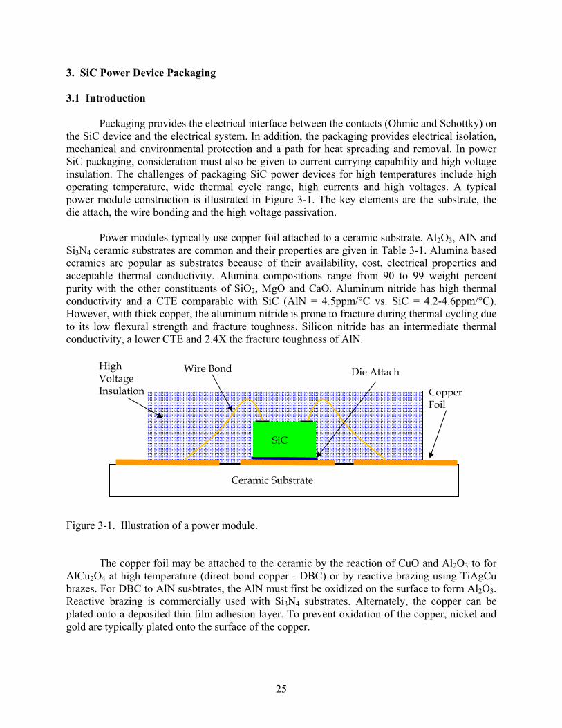
3. SiC Power Device Packaging 3.1 Introduction
Packaging provides the electrical interface between the contacts (Ohmic and Schottky) on the SiC device and the electrical system. In addition, the packaging provides electrical isolation, mechanical and environmental protection and a path for heat spreading and removal. In power SiC packaging, consideration must also be given to current carrying capability and high voltage insulation. The challenges of packaging SiC power devices for high temperatures include high operating temperature, wide thermal cycle range, high currents and high voltages. A typical power module construction is illustrated in Figure 3-1. The key elements are the substrate, the die attach, the wire bonding and the high voltage passivation.
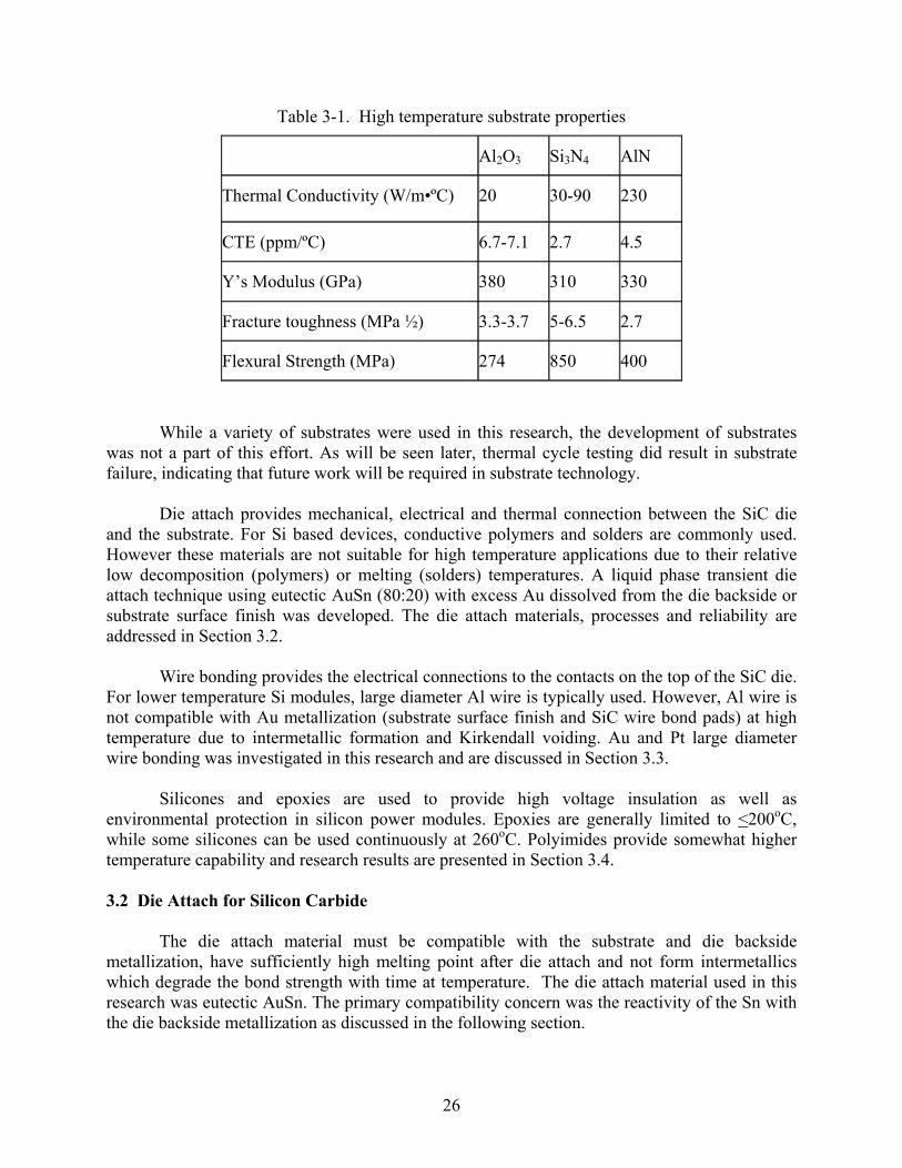
Power modules typically use copper foil attached to a ceramic substrate. Al2O3, AlN and
Si3N4 ceramic substrates are common and their properties are given in Table 3-1. Alumina based ceramics are popular as substrates because of their availability, cost, electrical properties and acceptable thermal conductivity. Alumina compositions range from 90 to 99 weight percent purity with the other constituents of SiO2, MgO and CaO. Aluminum nitride has high thermal conductivity and a CTE comparable with SiC (AlN = 4.5ppm/°C vs. SiC = 4.2-4.6ppm/°C). However, with thick copper, the aluminum nitride is prone to fracture during thermal cycling due to its low flexural strength and fracture toughness. Silicon nitride has an intermediate thermal conductivity, a lower CTE and 2.4X the fracture toughness of AlN.
Figure 3-1. Illustration of a power module.
The copper foil may be attached to the ceramic by the reaction of CuO and Al2O3 to for AlCu2O4 at high temperature (direct bond copper - DBC) or by reactive brazing using TiAgCu brazes. For DBC to AlN susbtrates, the AlN must first be oxidized on the surface to form Al2O3. Reactive brazing is commercially used with Si3N4 substrates. Alternately, the copper can be plated onto a deposited thin film adhesion layer. To prevent oxidation of the copper, nickel and gold are typically plated onto the surface of the copper.
Ceramic Substrate
SiC
Wire Bond Die Attach High Voltage Insulation Copper
Foil
26
Table 3-1. High temperature substrate properties
Al2O3 Si3N4 AlN
Thermal Conductivity (W/m•ºC) 20 30-90 230
CTE (ppm/ºC) 6.7-7.1 2.7 4.5
Y’s Modulus (GPa) 380 310 330
Fracture toughness (MPa ½) 3.3-3.7 5-6.5 2.7
Flexural Strength (MPa) 274 850 400
While a variety of substrates were used in this research, the development of substrates
was not a part of this effort. As will be seen later, thermal cycle testing did result in substrate failure, indicating that future work will be required in substrate technology.
Die attach provides mechanical, electrical and thermal connection between the SiC die and the substrate. For Si based devices, conductive polymers and solders are commonly used. However these materials are not suitable for high temperature applications due to their relative low decomposition (polymers) or melting (solders) temperatures. A liquid phase transient die attach technique using eutectic AuSn (80:20) with excess Au dissolved from the die backside or substrate surface finish was developed. The die attach materials, processes and reliability are addressed in Section 3.2. Wire bonding provides the electrical connections to the contacts on the top of the SiC die. For lower temperature Si modules, large diameter Al wire is typically used. However, Al wire is not compatible with Au metallization (substrate surface finish and SiC wire bond pads) at high temperature due to intermetallic formation and Kirkendall voiding. Au and Pt large diameter wire bonding was investigated in this research and are discussed in Section 3.3. Silicones and epoxies are used to provide high voltage insulation as well as environmental protection in silicon power modules. Epoxies are generally limited to <200oC, while some silicones can be used continuously at 260oC. Polyimides provide somewhat higher temperature capability and research results are presented in Section 3.4. 3.2 Die Attach for Silicon Carbide The die attach material must be compatible with the substrate and die backside metallization, have sufficiently high melting point after die attach and not form intermetallics which degrade the bond strength with time at temperature. The die attach material used in this research was eutectic AuSn. The primary compatibility concern was the reactivity of the Sn with the die backside metallization as discussed in the following section.

27
Chip metallization An effective chip metallization should provide the following features:
• Good adhesion to the wafer passivation and the contact (Ohmic or Schottky) • Low contact resistance • An effective diffusion barrier • A metal stack that is compatible with wire bonding and die attach metallurgy • High temperature reliability
Evaporation and sputtering are two of the most important physical vapor deposition (PVD) methods used for depositing thin metal films. Sputtering offers several advantages over evaporation due to its better film adhesion and ability to deposit alloys. The backside metallization initially studied was Ni2Si/Ti/Pt/Au. A 150mil x 150 mil SiC test die was used for brazing studies. The early shear tests results were: Sn-Au Braze - Backside Ti/Pt/Au (chip size 150x150)
a) initial: 82 kg, over 100kg b) 100 hrs @ 350oC: 39 kg, 47kg c) 408 hrs @ 350oC: 85kg, 73kg
The test limit with the Dage PC2400 shear tester is 100kg. While the shear strengths are high for the size of the die, higher shear strengths were targeted. Also, the lower shear strength after aging was a concern due to intermetallic formation between the Sn and the Pt. A backside metallization system based on NiCr (Cr/NiCr/Au: 2000Å /1000Å /4000Å) was developed using the sputtering system in the Physics Department at Auburn. With this die backside metallization deposited on SiC/SiO2, the die shear strength initially and after 2000 hours at 350oC was >100kg. This metal stack (Cr/NiCr/Au: 1000Å /1000Å /2050Å) was also deposited over SiC. The die shear strength initially and after 500 hours at 350oC was >100kg. The metal stack (Cr/NiCr/Au: 2000Å /1000Å /2000Å) was also deposited over SiC/Ni2Si in the Electrical Engineering Department at Auburn University. Again, the die shear strength initially and after 500 hours at 350oC was >100kg. Cr does not form intermetallics with Sn and this appeared to be a potential backside metallization stack. However, the process was not be successfully transferred to industry. The initial die shear strength for the metal stack (Cr/NiCr/Au: 2000Å /1000Å /2000Å) deposited in industry was 46, 41, 26, 26, 15kg. Ti/Ti-W/Au metallization stacks had also been developed in the industry. A sputtered three layer thin film stack composed of Ti/Ti-W/Au (1000 Å /2000 Å /2000 Å) was subsequently evaluated as the chip metallization in this project. Ti provides good adhesion to the device contacts (Ni2Si, an ohmic contact); Ti-90W functions as a diffusion barrier layer; and Au protects the underlying Ti-W from oxidation, as well as serving as a wire bondable and braze wettable surface. Sn does not form intermetallics with W, but does with Au, Ti and Ni. Ni will be present from the substrate surface finish as well as residual Ni after the formation of the
28
Ni2Si on the SiC die. Initial results with this backside metallization were excellent (die shear >100kg) and are discussed in detail in the following section.
Die Attach
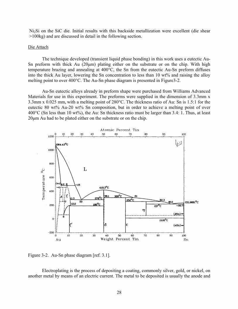
The technique developed (transient liquid phase bonding) in this work uses a eutectic Au-Sn preform with thick Au (20μm) plating either on the substrate or on the chip. With high temperature brazing and annealing at 400°C, the Sn from the eutectic Au-Sn preform diffuses into the thick Au layer, lowering the Sn concentration to less than 10 wt% and raising the alloy melting point to over 400°C. The Au-Sn phase diagram is presented in Figure3-2.
Au-Sn eutectic alloys already in preform shape were purchased from Williams Advanced
Materials for use in this experiment. The preforms were supplied in the dimension of 3.3mm x 3.3mm x 0.025 mm, with a melting point of 280°C. The thickness ratio of Au: Sn is 1.5:1 for the eutectic 80 wt% Au-20 wt% Sn composition, but in order to achieve a melting point of over 400°C (Sn less than 10 wt%), the Au: Sn thickness ratio must be larger than 3.4: 1. Thus, at least 20μm Au had to be plated either on the substrate or on the chip.
Figure 3-2. Au-Sn phase diagram [ref. 3.1].
Electroplating is the process of depositing a coating, commonly silver, gold, or nickel, on another metal by means of an electric current. The metal to be deposited is usually the anode and
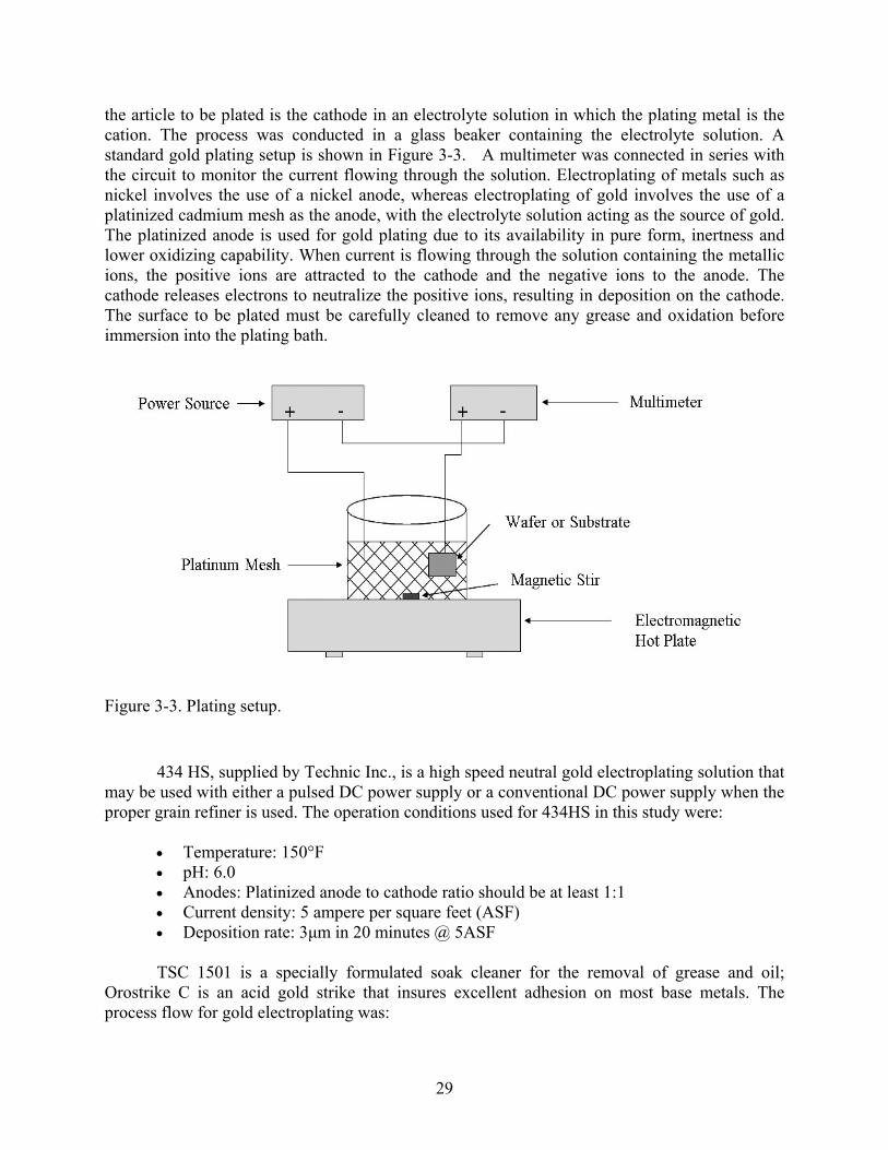
29
the article to be plated is the cathode in an electrolyte solution in which the plating metal is the cation. The process was conducted in a glass beaker containing the electrolyte solution. A standard gold plating setup is shown in Figure 3-3. A multimeter was connected in series with the circuit to monitor the current flowing through the solution. Electroplating of metals such as nickel involves the use of a nickel anode, whereas electroplating of gold involves the use of a platinized cadmium mesh as the anode, with the electrolyte solution acting as the source of gold. The platinized anode is used for gold plating due to its availability in pure form, inertness and lower oxidizing capability. When current is flowing through the solution containing the metallic ions, the positive ions are attracted to the cathode and the negative ions to the anode. The cathode releases electrons to neutralize the positive ions, resulting in deposition on the cathode. The surface to be plated must be carefully cleaned to remove any grease and oxidation before immersion into the plating bath.
Figure 3-3. Plating setup.
434 HS, supplied by Technic Inc., is a high speed neutral gold electroplating solution that may be used with either a pulsed DC power supply or a conventional DC power supply when the proper grain refiner is used. The operation conditions used for 434HS in this study were:
• Temperature: 150°F • pH: 6.0 • Anodes: Platinized anode to cathode ratio should be at least 1:1 • Current density: 5 ampere per square feet (ASF) • Deposition rate: 3μm in 20 minutes @ 5ASF TSC 1501 is a specially formulated soak cleaner for the removal of grease and oil;
Orostrike C is an acid gold strike that insures excellent adhesion on most base metals. The process flow for gold electroplating was:

30
• TSC 1501 soak clean for two minutes at 65°C • DI water rinse • Degrease in a diluted 19:1 Deionized water: sulfacid solution for two minutes • DI water rinse • Orostrike C for 30 seconds @ 7.5 ASF, 40°C • DI water rinse • 434 HS plating, with the plating time dependent on the thickness required • DI water rinse
A cross-section of a DBC Al2O3 substrate electroplated with 20μm Au is shown in Figure 3-4.
The brazing process was performed with an SST 3150 high vacuum furnace. The 3150 utilizes an oil-free roughing pump and a turbomolecular drag pump to achieve vacuum levels as low as 10-6 torr at temperatures of up to 500 °C. The brazing process can be done either in vacuum or in an inert gas with a pressure of up to 15 psig. Voids in the bonding layer will significantly hinder the heat transfer from the chip to the substrate and weaken the braze joint strength. In order to obtain a void-free bond, the process was run in vacuum, and a 20g weight was placed on the assembly to squeeze out any remaining air bubbles. An illustration of the brazing setup is shown in Figure 3-5. The chip size was 150mil x 150mil with Ti/Ti-W/Au (20μm) metallization, and the DBC Al2O3 substrate size was 200 mil x 200mil. The specially designed brazing profile is presented in Figures 3-6 a and b. It includes a four minute soak at 250°C to bake out residual moisture, then a 3 hour ramp from 250°C to 400°C, followed by a hold at 400°C for 30 minutes to allow Sn to diffuse into the Au layer.
Figure 3-4. DBC Al2O3 substrate electroplated with 20μm Au.
Ni
Cu
Au
Ni
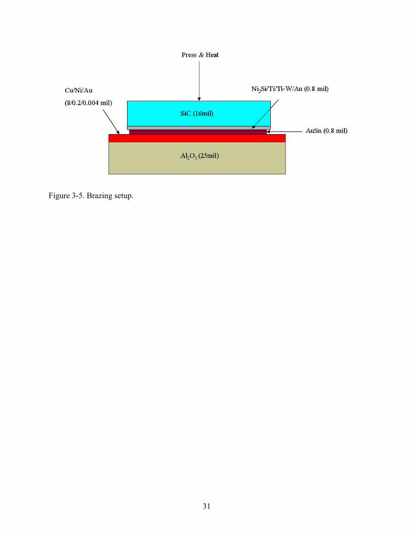
31
Figure 3-5. Brazing setup.

32
(a) Temperature
(b) Pressure
Figure 3-6. AuSn brazing profile.

33
An optical image of an as-brazed sample is shown in Figure 3-7 (a), a void-free die attach was achieved, as shown in the x-ray relief mode image in Figure 3-7 (b). The bond strength was evaluated by a die shear test utilizing the Dage PC2400 system. The average as-brazed sample die shear strength was > 100kg-f (equipment limit). The sample size was 7.
(a) (b)
Figure 3-7. (a) as-brazed sample and (b) x-ray relief mode picture of as-brazed sample. Figure 3-8 shows the energy dispersive x-ray (EDX) elemental concentration plot across an AuSn as-brazed sample. The Sn concentration is about 6 wt% across the brazing layer, which corresponds to the Sn solid solubility limit in Au at 400°C. The Sn peak at the chip interface represents the reaction of Sn with Ti in the SiC metallization to form Sn-Ti intermetallic, while the Sn peak at the substrate surface is due to Sn-Ni intermetallic formation. Figure 3-9 shows the EDX element dot maps for an AuSn as-brazed sample, which show that the Sn is uniformly distributed throughout the Au layer, except for a peak at the substrate and the chip interface.

34
0
10
20
30
40
50
60
70
80
90
100
-6 0 6 11 17 22 28 34 39 45
Approximate distance from surface of ceramic (μm)
Com
posi
tion
(wt.%
)AuSnCuNiPTiWSi
Figure 3-8. Element concentration plot across an AuSn as-brazed sample.

35
Figure 3-9. EDX elemental dot maps for an AuSn as-brazed sample.
Au Ni
SEI Cu
Sn Ti

36
3.2.1 Reliability Testing High Temperature Storage Test
A high temperature storage test was used to determine the effect of time and temperature on the die shear strength. The apparatus used for this test was a Blue-M burn in chamber maintained at 400°C.
In order to study the effect of Ni as a diffusion barrier and reaction layer, two types of DBC Al2O3 substrate were used in this test: DBC Al2O3 with electroless plated Ni:P and DBC Al2O3 with electrolytic plated Ni. The Ni layers were about 6μm thick, protected by a 0.10~0.20μm layer of immersion Au (IG). To lower the Sn concentration to less than 10wt%, a thick Au (20μm) layer was required, and two types of thick Au metallization were used in this study: thick Au on the chip backside and thick Au on the substrate. It is easier to electroplate the whole wafer (dicing the whole wafer into individual chips afterward) than to electroplate the individual DBC Al2O3 substrates, which is time consuming. On the other hand, with the IG surface finish, Ni and Cu will diffuse through the IG to the top of the substrate surface and oxidize in air during high temperature storage, so a thick Au layer (20μm) on the substrate was also used to test the effectiveness of this Au layer in retarding the diffusion and subsequent oxidation of the underlying Ni and Cu layers. In summary, four kinds of samples were built for the high temperature storage test:
• DBC on Al2O3 with electroless Ni:P, thick Au on substrate • DBC on Al2O3 with electroless Ni:P, thick Au on chip • DBC on Al2O3 with electrolytic Ni, thick Au on substrate • DBC on Al2O3 with electrolytic Ni, thick Au on chip
The samples were tested at 100 hours, 250 hours, 500 hours, 1000 hours and 2000 hours with a group sample size of seven. A die shear test was used to evaluate the braze joint strength, and a cross-section sample was subjected to scanning electron microscopy /energy dispersive x-ray (SEM/EDX) analysis in order to detect intermetallic compound (IMC) formation and elemental interdiffusion during high temperature storage.
Figure 3-10 shows the die shear values for the four types of sample after aging at 400ºC. The Dage PC 2400 used to perform this test has a 100kg-f shear strength limit. The die shear strength of the electrolytic Ni samples (both thick Au on substrate and on chip) did not degrade after 2000 hours of thermal storage. However, the average die shear strength of the electroless Ni:P samples with Au on the substrate and Au on the chip degraded to 77.2kg and 73.6kg, respectively after 2000 hours aging at 400ºC in air.
Figure 3-11 shows an EDX element concentration cross-section plot of the sample after 2000 hours storage at 400ºC, and Figure 12 presents an EDX element composition cross-section analysis of the braze interface. In these two figures, the metallization of the DBC Al2O3 substrate

37
was Cu/ Ni:P/ immersion Au, with a thick Au (20µm) layer on the chip. By carefully studying these results, the following conclusions can be drawn:
1. Sn formed intermetallic compounds with Ti, resulting in higher Sn concentrations at the die surface.
2. A semi-continuous Ni:P:Cu layer formed during aging. 3. The AuSn braze layer was almost depleted of Sn, with only a residual level (about 1
wt%) of Sn remaining in the layer. Sn continued to react with Ni and Au, forming intermetallic compounds during aging. The Ni-Sn-Au intermetallic compounds were separated from the Ni:P:Cu under layer by a layer of 85 wt% Au-15 wt% Cu.
4. Cu was able to diffuse through the Ni:P and was found everywhere in the Au layer. Au was only able to diffuse into the Cu layer at the location where the Ni:P:Cu layer was broken.
0
20
40
60
80
100
Initial 100 hrs 250 hrs 500 hrs 1000 hrs 2000hrs
Aging Time
Die
shea
r stre
ngth
(Kg) 6μm Ni:P/ 20μm Au; thin Au
on chip6μm Ni:P; 20μm Au on chip
6μm Ni/ 20μm Au; thin Au onchip6μm Ni; 20μm Au on chip
Figure 3-10. Die shear strength as a function of aging at 400ºC in air.

38
0
10
20
30
40
50
60
70
80
90
100
-4 0 4 8 12 16 20 24 28 32 36 40 44 48 52 56 60
Approximate distance from bond/substrate interface (μm)
Com
posi
tion
(wt.
%)
AuSnCuNiPTiWSi
Figure 3-11. Element concentration plot across an AuSn brazed sample after 2000 hours storage at 400ºC, electroless Ni:P, thick Au on chip.

39
89%Au, 10%Cu, 1%Sn
52%Sn, 31%Ni, 17%Au85%Au, 15%Cu
81%Ni, 14%P, 5%Cu
60%Au, 40%Cu
All compositions are in weight percent
89%Au, 10%Cu, 1%Sn
52%Sn, 31%Ni, 17%Au85%Au, 15%Cu
81%Ni, 14%P, 5%Cu
60%Au, 40%Cu
All compositions are in weight percent
89%Au, 10%Cu, 1%Sn89%Au, 10%Cu, 1%Sn
52%Sn, 31%Ni, 17%Au52%Sn, 31%Ni, 17%Au85%Au, 15%Cu85%Au, 15%Cu
81%Ni, 14%P, 5%Cu81%Ni, 14%P, 5%Cu
60%Au, 40%Cu60%Au, 40%Cu
All compositions are in weight percent
(a)
90%Au, 9%Cu, 1%Sn
52%Sn, 32%Ni, 16%Au
87%Au, 13%Cu
82%Ni, 15%P, 3%Cu100%Cu
All compositions are in weight percent
90%Au, 9%Cu, 1%Sn
52%Sn, 32%Ni, 16%Au
87%Au, 13%Cu
82%Ni, 15%P, 3%Cu100%Cu
All compositions are in weight percent
(b)
Figure 3-12. Cross-section of die attach after 2000 hours at 400ºC, electroless Ni:P, thick Au on chip, (a) at Ni:P:Cu broken area and (b) at Ni:P:Cu continuous area.
Figure 3-12 (a) shows voids that developed at the Cu-Ni:P interface after 1000 hours aging at 400ºC, and Figure 3-12 (b) shows a crack that developed at the Cu-Ni:P interface after 2000 hours aging at 400ºC. The Kirkendall effect may explain why the voids and cracks occurred. The Kirkendall effect is the formation of voids due to the different interdiffusion rate between two neighboring materials. Cu and Au are completely miscible. During high temperature aging, Cu diffuses into the Ni and Au layers, but at the same time there is negligible diffusion of Ni and Au in the opposite direction into the Cu at the Cu-Ni:P interface (Figure 3-12 (b)). The Ni:P layer is an effective barrier to Au diffusion (except in Figure 3-12 (a) where the

40
layer is physically broken. The net result is that atomic vacancies are generated in the Cu to preserve the mass balance. As the diffusion proceeds, the vacancy concentration increases until super-saturation occurs, resulting in nucleation and the growth of voids.
The different interdiffusion rate across the Ni:P layer caused voids to occur at the Cu-Ni:P interface after 1000 hours aging at 400ºC (Figure 3-13 (a)) and the coalescence of these voids resulted in the cracks at the Cu-Ni:P interface after 2000 hours (Figure 3-13 (b)) thermal storage. The lower die shear strength was due to occurrence of these cracks.
Figure 3-14 shows an EDX element concentration cross-section plot of the electrolytic Ni sample after 2000 hours storage at 400ºC, and Figure 3-15 presents an EDX element composition cross-section analysis of the braze interface after 2000 hours storage at 400ºC. In both these figures, the metallization of the DBC Al2O3 substrate was Cu/Ni/Au (20µm). By carefully studying these results, it is possible to draw the following conclusions:
1. A series of intermetallic compounds was formed, consuming the Sn and the Ni layer. 2. Cu was able to diffuse through the Ni into the Au layer. 3. The complex intermetallics formed had good adhesion and strength after aging.
(a) (b)
Figure 3-13. Cross-section of the die attach, (a) voids at Cu-Ni:P interface after 1000 hours aging and (b) cracks at Cu-Ni:P interface after 2000 hours aging at 400ºC.
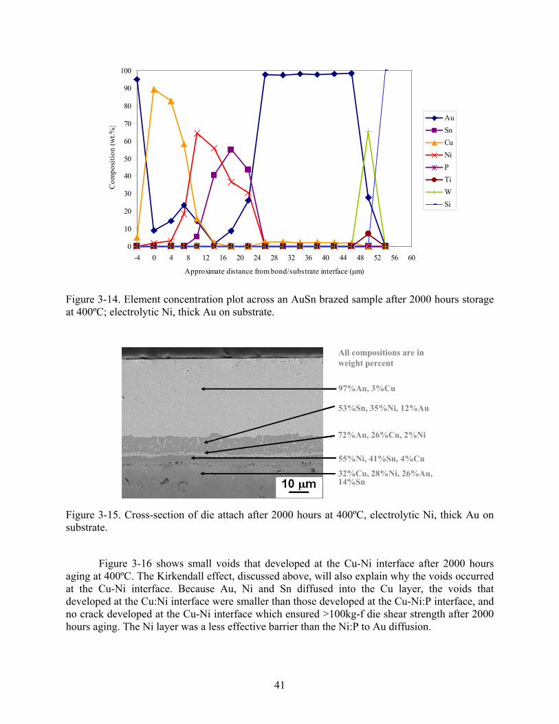
41
0
10
20
30
40
50
60
70
80
90
100
-4 0 4 8 12 16 20 24 28 32 36 40 44 48 52 56 60
Approximate distance from bond/substrate interface (μm)
Com
posi
tion
(wt.%
)AuSnCuNiPTiWSi
Figure 3-14. Element concentration plot across an AuSn brazed sample after 2000 hours storage at 400ºC; electrolytic Ni, thick Au on substrate.
97%Au, 3%Cu
53%Sn, 35%Ni, 12%Au
72%Au, 26%Cu, 2%Ni
55%Ni, 41%Sn, 4%Cu
32%Cu, 28%Ni, 26%Au, 14%Sn
All compositions are in weight percent
97%Au, 3%Cu
53%Sn, 35%Ni, 12%Au
72%Au, 26%Cu, 2%Ni
55%Ni, 41%Sn, 4%Cu
32%Cu, 28%Ni, 26%Au, 14%Sn
All compositions are in weight percent
Figure 3-15. Cross-section of die attach after 2000 hours at 400ºC, electrolytic Ni, thick Au on substrate.
Figure 3-16 shows small voids that developed at the Cu-Ni interface after 2000 hours
aging at 400ºC. The Kirkendall effect, discussed above, will also explain why the voids occurred at the Cu-Ni interface. Because Au, Ni and Sn diffused into the Cu layer, the voids that developed at the Cu:Ni interface were smaller than those developed at the Cu-Ni:P interface, and no crack developed at the Cu-Ni interface which ensured >100kg-f die shear strength after 2000 hours aging. The Ni layer was a less effective barrier than the Ni:P to Au diffusion.

42
Figure 3-16. Cross-section of the die attach, showing voids at Cu-Ni interface after 2000 hours aging at 400ºC.
A second test was performed to validate the die shear test results using DBC Al2O3 substrates with electrolytic Ni and electroless N:P at both 1µm and 6µm thickness. The die shear data for the samples built with 6µm Ni (both electrolytic Ni and electroless Ni:P) DBC Al2O3 substrates replicated the original results, as shown in Figure 3-17. Figure 3-18 shows the die shear strengths for the samples built with 1μm Ni (both electrolytic Ni and electroless Ni:P) DBC Al2O3
0
20
40
60
80
100
Initial 100 hrs 250 hrs 500 hrs 1000 hrs 2000hrs
Aging Time
Die
shea
r stre
ngth
(Kg) 6μm Ni:P/ 20μm Au; thin Au
on chip6μm Ni:P; 20μm Au on chip
6μm Ni/ 20μm Au; thin Au onchip6μm Ni; 20μm Au on chip
Figure 3-17. Die shear strength as a function of aging, confirmation test, 6 µm Ni DBC Al2O3 substrates, 400ºC in air.
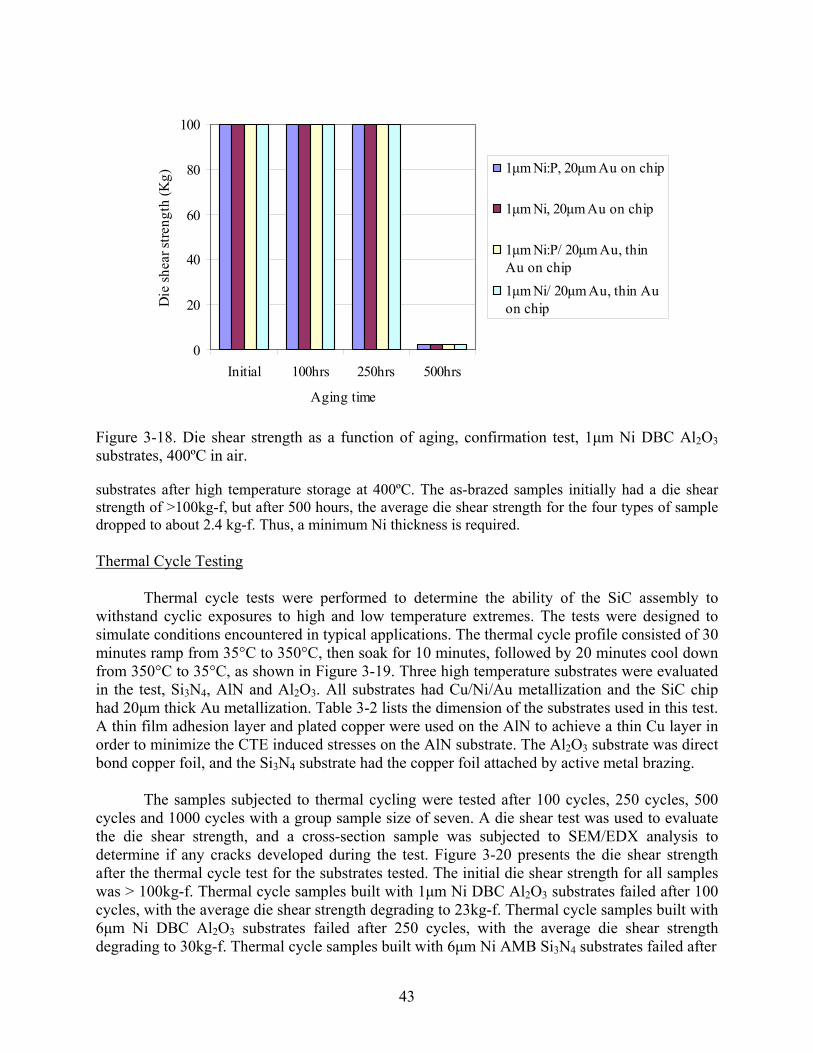
43
0
20
40
60
80
100
Initial 100hrs 250hrs 500hrs
Aging time
Die
shea
r stre
ngth
(Kg) 1μm Ni:P, 20μm Au on chip
1μm Ni, 20μm Au on chip
1μm Ni:P/ 20μm Au, thinAu on chip1μm Ni/ 20μm Au, thin Auon chip
Figure 3-18. Die shear strength as a function of aging, confirmation test, 1μm Ni DBC Al2O3 substrates, 400ºC in air.
substrates after high temperature storage at 400ºC. The as-brazed samples initially had a die shear strength of >100kg-f, but after 500 hours, the average die shear strength for the four types of sample dropped to about 2.4 kg-f. Thus, a minimum Ni thickness is required. Thermal Cycle Testing
Thermal cycle tests were performed to determine the ability of the SiC assembly to withstand cyclic exposures to high and low temperature extremes. The tests were designed to simulate conditions encountered in typical applications. The thermal cycle profile consisted of 30 minutes ramp from 35°C to 350°C, then soak for 10 minutes, followed by 20 minutes cool down from 350°C to 35°C, as shown in Figure 3-19. Three high temperature substrates were evaluated in the test, Si3N4, AlN and Al2O3. All substrates had Cu/Ni/Au metallization and the SiC chip had 20μm thick Au metallization. Table 3-2 lists the dimension of the substrates used in this test. A thin film adhesion layer and plated copper were used on the AlN to achieve a thin Cu layer in order to minimize the CTE induced stresses on the AlN substrate. The Al2O3 substrate was direct bond copper foil, and the Si3N4 substrate had the copper foil attached by active metal brazing.
The samples subjected to thermal cycling were tested after 100 cycles, 250 cycles, 500
cycles and 1000 cycles with a group sample size of seven. A die shear test was used to evaluate the die shear strength, and a cross-section sample was subjected to SEM/EDX analysis to determine if any cracks developed during the test. Figure 3-20 presents the die shear strength after the thermal cycle test for the substrates tested. The initial die shear strength for all samples was > 100kg-f. Thermal cycle samples built with 1μm Ni DBC Al2O3 substrates failed after 100 cycles, with the average die shear strength degrading to 23kg-f. Thermal cycle samples built with 6μm Ni DBC Al2O3 substrates failed after 250 cycles, with the average die shear strength degrading to 30kg-f. Thermal cycle samples built with 6μm Ni AMB Si3N4 substrates failed after
44
500 cycles, with the average die shear strength degrading to 25kg-f. Thermal cycle samples built with thin film/plated Cu AlN substrates had an average die shear strength > 100kg-f after 1000 cycles.
050
100150200250300350400
0 50 100 150 200Time (min.)
Tem
pera
ture
(°C
)
FrontCenterEnd
Figure 3-19. Thermal cycle test profile.
Table 3-2. Substrates dimensions
Substrate Size (mil2)
Ceramic
Thickness (μm)
Cu
Thickness (μm)
Ni
Thickness (μm)
Type of Cu
AlN 1000x1000 255 45 3 Thin film/plated
Si3N4 200x200 642 154 6 AMB
Al2O3 200x200 630 190 6 DBC
Al2O3 1000x1000 630 250 1 DBC After 100 cycles, the direct bond Cu foil delaminated from the 1μm Ni Al2O3 substrate.
Figure 3-21 shows the Auger emission spectroscopy (AES) analysis results on the delaminated substrate surface and Cu foil surface. Al, Si, Ca, O and C were detected on both surfaces. Al, Si, Ca and O are the composition elements of the Al2O3 substrate, while the C is a common contaminate on sample surface exposed to the atmosphere. It was also observed that no Cu
45
remained on the Al2O3 substrate, and the Cu foil was covered with a thin layer of Al2O3, so it is reasonable to conclude that the Al2O3 substrate surface fractured during the thermal cycle test as a result of the CTE mismatch induced stresses between the Cu foil and Al2O3 substrate.
0
20
40
60
80
100
Initial 100cycles
250cycles
500cycles
1000cycles
Thermal cycle numbers
Die
shea
r stre
ngth
(Kg) Al2O3 (1μm Ni)
Al2O3 (6μm Ni)Si3N4AlN
Figure 3-20. Die shear strength as a function of thermal cycle numbers.

46
(a)
(b)
Figure 3-21. AES results after 100 thermal cycles, DBC Al2O3 substrate with 1μm electroless Ni:P, (a) Cu foil surface and (b) substrate surface.
47
Figure 3-22. Cross-section of braze layer after 100 thermal cycles, showing crack in braze layer and braze-TiW delamination. DBC Al2O3 with 1μm electrolytic Ni.
Figure 3-23. Cross-section of braze layer after 100 thermal cycles, showing crack in braze layer and braze-TiW delamination. DBC Al2O3 with 1μm electroless Ni:P.
Cracks in the braze layer and braze-TiW delamination also developed during thermal cycling. Figures 3-22 and Figure 3-23 show cross-section pictures of the samples with the 1μm electrolytic Ni DBC Al2O3 substrate and 1μm electroless Ni:P DBC Al2O3 substrate after 100 cycles, showing the braze crack and braze-TiW delamination that developed during thermal cycling.
The direct bond Cu foil delaminated from the Al2O3 substrate with 6μm Ni after 250 cycles, as shown in Figure 3-24. By comparison the two types of DBC Al2O3 substrates (1μm Ni vs. 6μm Ni), it was found that the substrates with thinner Cu foil (190μm vs. 250μm) had better thermal cycling performance due to the less CTE mismatch induced stress exerted on the Al2O3 surface.

48
Figure 3-24. Cu foil delamination after 250 thermal cycles.
Figure 3-25. Cross-section of braze layer after 250 thermal cycles, showing cracks in the braze layer and braze-TiW delamination. DBC Al2O3 substrate with 6μm electrolytic Ni.
Figure 3-26. Cross-section of braze layer after 250 thermal cycles, showing cracks in the braze layer and braze-TiW delamination. DBC Al2O3 substrate with 6μm electroless Ni:P.
49
Figures 3-25 and 3-26 show cross-section pictures of the samples built with the 6μm electrolytic Ni DBC Al2O3 substrate and 6μm electroless Ni:P DBC Al2O3 substrate after 250 cycles, showing that braze cracking and braze-TiW delamination developed during thermal cycling.
Figure 3-27(a) shows an x-ray image of the DBC Al2O3 substrate (after the die shear test) in relief mode, showing the cracks that developed in the braze layer during thermal cycling. Figure 3-27(b) shows an x-ray image of the corresponding chip (after the die shear test) in void calculation mode in order to calculate how much braze remained on the chip. The white area represents the AuSn braze residue. In total, the chip had 21.7% of its area covered by braze residue. Since most of the chip area was free of braze residue, the braze-TiW delamination was a major failure mode compared to the cracks that developed in braze layer.
AES analyses of the surface of the substrate and chip are shown in Figure 3-28. Here, the
elements Au, Sn, Ti, and W are present on both the substrate surface and chip surface, although the intensity of the Sn on the substrate side and Ti on the chip side are significantly higher, and the elements C and O are the adventitious surface contaminates that are present on any “as received” sample exposed to air. The results proved that braze-chip delamination occurred at the braze-TiW interface.
(a) (b)
Figure 3-27. (a) X-ray image in relief mode, showing cracks in the braze layer and (b) x-ray image in voids calculation mode, calculating braze residue area percentage on chip surface; DBC Al2O3 substrate with 6μm electroless Ni:P after 250 thermal cycles.

50
(a)
(b)
Figure 3-28. AES results after 250 thermal cycles, DBC Al2O3 with 6μm electroless Ni:P, (a) substrate side and (b) chip side.
Thermal cycling samples built with Si3N4 substrates failed at 500 cycles. Figure 3-29 shows an optical image of the Si3N4 assembly after 500 thermal cycles. The bottom copper foil delaminated from the Si3N4 substrate, but the top copper metallization only delaminated slightly at the edges because the SiC chip helped constrain the Cu. Figure 3-30 shows the AES analysis results for the delaminated copper foil surface and the corresponding substrate surface. Si, N, Cl,
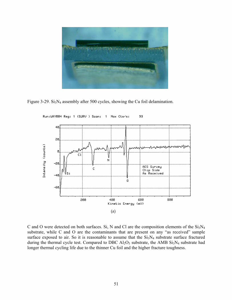
51
Figure 3-29. Si3N4 assembly after 500 cycles, showing the Cu foil delamination.
(a) C and O were detected on both surfaces. Si, N and Cl are the composition elements of the Si3N4 substrate, while C and O are the contaminants that are present on any “as received” sample surface exposed to air. So it is reasonable to assume that the Si3N4 substrate surface fractured during the thermal cycle test. Compared to DBC Al2O3 substrate, the AMB Si3N4 substrate had longer thermal cycling life due to the thinner Cu foil and the higher fracture toughness.
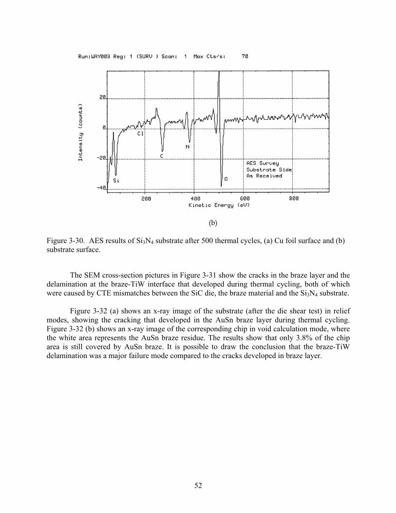
52
(b) Figure 3-30. AES results of Si3N4 substrate after 500 thermal cycles, (a) Cu foil surface and (b) substrate surface.
The SEM cross-section pictures in Figure 3-31 show the cracks in the braze layer and the delamination at the braze-TiW interface that developed during thermal cycling, both of which were caused by CTE mismatches between the SiC die, the braze material and the Si3N4 substrate.
Figure 3-32 (a) shows an x-ray image of the substrate (after the die shear test) in relief
modes, showing the cracking that developed in the AuSn braze layer during thermal cycling. Figure 3-32 (b) shows an x-ray image of the corresponding chip in void calculation mode, where the white area represents the AuSn braze residue. The results show that only 3.8% of the chip area is still covered by AuSn braze. It is possible to draw the conclusion that the braze-TiW delamination was a major failure mode compared to the cracks developed in braze layer.
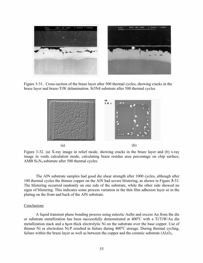
53
Figure 3-31. Cross-section of the braze layer after 500 thermal cycles, showing cracks in the braze layer and braze-TiW delamination. Si3N4 substrate after 500 thermal cycles.
(a) (b)
Figure 3-32. (a) X-ray image in relief mode, showing cracks in the braze layer and (b) x-ray image in voids calculation mode, calculating braze residue area percentage on chip surface; AMB Si3N4 substrate after 500 thermal cycles.
The AlN substrate samples had good die shear strength after 1000 cycles, although after 100 thermal cycles the thinner copper on the AlN had severe blistering, as shown in Figure 3-33. The blistering occurred randomly on one side of the substrate, while the other side showed no signs of blistering. This indicates some process variation in the thin film adhesion layer or in the plating on the front and back of the AlN substrate. Conclusions A liquid transient phase bonding process using eutectic AuSn and excess Au from the die or substrate metallization has been successfully demonstrated at 400oC with a Ti/TiW/Au die metallization stack and a 6μm thick electrolytic Ni on the substrate over the base copper. Use of thinner Ni or electroless Ni:P resulted in failure during 400oC storage. During thermal cycling, failure within the braze layer as well as between the copper and the ceramic substrate (Al2O3,
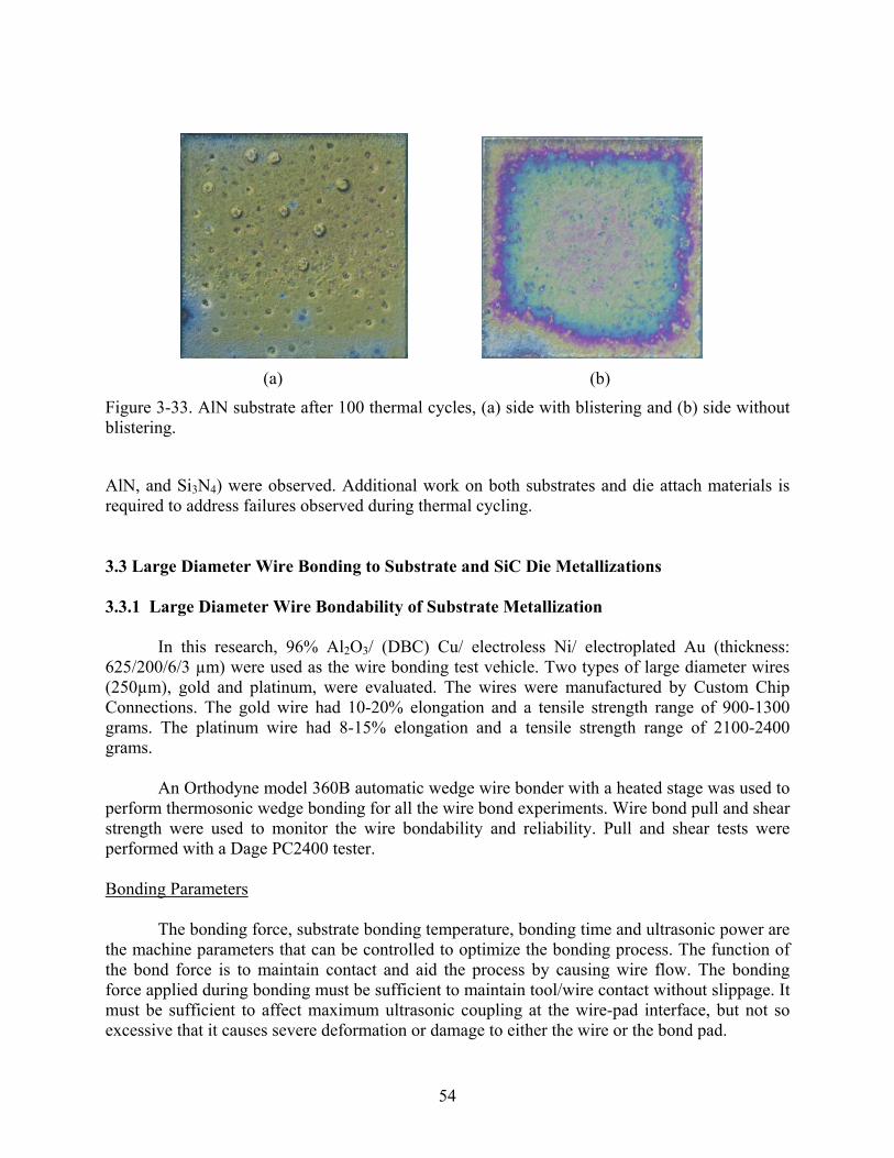
54
(a) (b)
Figure 3-33. AlN substrate after 100 thermal cycles, (a) side with blistering and (b) side without blistering.
AlN, and Si3N4) were observed. Additional work on both substrates and die attach materials is required to address failures observed during thermal cycling. 3.3 Large Diameter Wire Bonding to Substrate and SiC Die Metallizations 3.3.1 Large Diameter Wire Bondability of Substrate Metallization In this research, 96% Al2O3/ (DBC) Cu/ electroless Ni/ electroplated Au (thickness: 625/200/6/3 µm) were used as the wire bonding test vehicle. Two types of large diameter wires (250µm), gold and platinum, were evaluated. The wires were manufactured by Custom Chip Connections. The gold wire had 10-20% elongation and a tensile strength range of 900-1300 grams. The platinum wire had 8-15% elongation and a tensile strength range of 2100-2400 grams. An Orthodyne model 360B automatic wedge wire bonder with a heated stage was used to perform thermosonic wedge bonding for all the wire bond experiments. Wire bond pull and shear strength were used to monitor the wire bondability and reliability. Pull and shear tests were performed with a Dage PC2400 tester. Bonding Parameters The bonding force, substrate bonding temperature, bonding time and ultrasonic power are the machine parameters that can be controlled to optimize the bonding process. The function of the bond force is to maintain contact and aid the process by causing wire flow. The bonding force applied during bonding must be sufficient to maintain tool/wire contact without slippage. It must be sufficient to affect maximum ultrasonic coupling at the wire-pad interface, but not so excessive that it causes severe deformation or damage to either the wire or the bond pad.
55
The bonding temperature at the bond site also plays an important role in the strength of the bond formed, having a more significant impact than even the ultrasonic energy used. The higher the temperature, the lower the ultrasonic energy required to form the bond. Providing extra energy to the bond site in the form of heat generally causes the process to be more robust and allows for a larger working window of the wire bonding parameters. For reliable thermosonic gold or platinum bonding, the wire bonding process requires a certain minimum temperature, after which increasing the bonding temperature will produce stronger thermosonic bonds. In general, the higher the temperature the greater the reaction rate and the shorter the time required for thermosonic bonding. However, very high bonding temperatures may cause damage to the components, oxidation of the metallization or raise other reliability issues, so the bonding temperature should be kept below 250°C.
Bond time is the time duration for the application of ultrasonic energy. If the bond time is
too short, insufficient wire deformation and bond formation occurs and bond lifts will be observed during pull tests. In contrast, excess bond time can result in damage to both the wire and the bond. As discussed above, if the bonding temperature is higher, the bonding time required for thermosonic bonding will be shorter. Compared to the bond force, bonding temperature and ultrasonic power, the bonding time is usually of lesser significance during the wire bond process.
Ultrasonic energy, coupled to the tool from a transducer, moves the bonding tool back
and forth along a line parallel to the axis of the wire. The wire begins to soften as the ultrasonic energy is absorbed at existing dislocations in the wire. The ultrasonic energy causes still more dislocations to form and eventually slip occurs at crystal planes on both sides of the bond site and wire, exposing metals along the new slip faces. As the interface is shielded from the surrounding air, the freshly exposed wire surface readily mixes with the substrate metallization and seizes, creating a metallurgical bond at the interface.
The amplitude of the vibration impacts the bond deformation: the amount of deformation
is directly proportional to the amplitude of the vibration. For the ultrasonic vibration frequency, if the amplitude is excessively high, there is a possibility of fracturing already bonded contact areas before the welding period is completed.
As the result of a comprehensive design of experiments methodology with different bonding parameters, the optimal bonding parameters were identified and used to wire bond test parts for high temperature storage testing. The following criteria were used to determine the optimal bonding parameters:
• Smallest number of bond misses • 100% residue left after shear test • Wire bonds with good destructive pull strengths • Wire bonds with good shear test strengths • Smallest number of bond lift failures during destructive pull testing • Deformation (< 1.2x wire diameter) • Smallest unbonded area in the center of the bond
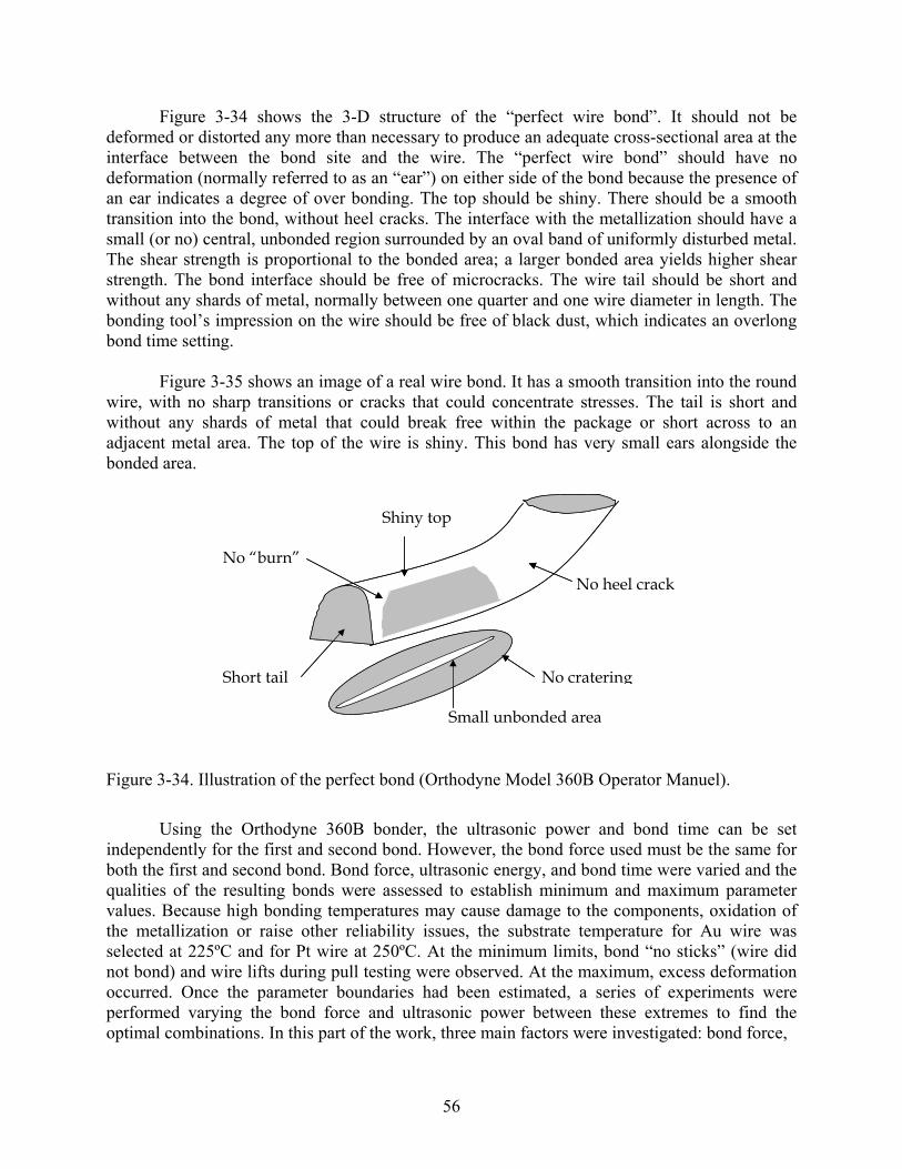
56
Figure 3-34 shows the 3-D structure of the “perfect wire bond”. It should not be deformed or distorted any more than necessary to produce an adequate cross-sectional area at the interface between the bond site and the wire. The “perfect wire bond” should have no deformation (normally referred to as an “ear”) on either side of the bond because the presence of an ear indicates a degree of over bonding. The top should be shiny. There should be a smooth transition into the bond, without heel cracks. The interface with the metallization should have a small (or no) central, unbonded region surrounded by an oval band of uniformly disturbed metal. The shear strength is proportional to the bonded area; a larger bonded area yields higher shear strength. The bond interface should be free of microcracks. The wire tail should be short and without any shards of metal, normally between one quarter and one wire diameter in length. The bonding tool’s impression on the wire should be free of black dust, which indicates an overlong bond time setting.
Figure 3-35 shows an image of a real wire bond. It has a smooth transition into the round
wire, with no sharp transitions or cracks that could concentrate stresses. The tail is short and without any shards of metal that could break free within the package or short across to an adjacent metal area. The top of the wire is shiny. This bond has very small ears alongside the bonded area.
Figure 3-34. Illustration of the perfect bond (Orthodyne Model 360B Operator Manuel). Using the Orthodyne 360B bonder, the ultrasonic power and bond time can be set independently for the first and second bond. However, the bond force used must be the same for both the first and second bond. Bond force, ultrasonic energy, and bond time were varied and the qualities of the resulting bonds were assessed to establish minimum and maximum parameter values. Because high bonding temperatures may cause damage to the components, oxidation of the metallization or raise other reliability issues, the substrate temperature for Au wire was selected at 225ºC and for Pt wire at 250ºC. At the minimum limits, bond “no sticks” (wire did not bond) and wire lifts during pull testing were observed. At the maximum, excess deformation occurred. Once the parameter boundaries had been estimated, a series of experiments were performed varying the bond force and ultrasonic power between these extremes to find the optimal combinations. In this part of the work, three main factors were investigated: bond force,
Shiny top
No “burn”
Short tail
No heel crack
Small unbonded area
No cratering

57
Shiny top Short tail No heel crack
Small ear No “burn”
Shiny top Short tail No heel crack
Small ear No “burn”
Figure 3-35. Photograph of a real bond. ultrasonic energy (bond power), and bond time. For example, the factors and levels of the first bond gold wire bonding are shown in Table 3-3, with the corresponding Taguchi 3k factorial design shown in Table 3-4. For each DOE run, 12 bonds were bonded and the shear strengths were collected for analysis.
Table 3-5 shows the ANOVA DOE analysis results. Figure 3-36 is the main effect plot for means based on shear strength. From Table 3-5 and Figure 3-36, time has no significant effect on shear strength, so a single time was selected and used for all experiments based on the initial results; bond force and power both have a significant effect on the shear strength. The 350 g-f bond force and 120 µinch bond power had the best shear strength. The optimal parameters selected as a result of this processes are shown in Table 3-6.
Table 3-3. Control factors and levels for DOE of wire bonding parameters
Controllable Factor Level 1 Level 2 Level 3 A: Force (g-f) 330 350 370 B: Power (µinch) 110 120 130 C: Time (µsec) 110 120 130
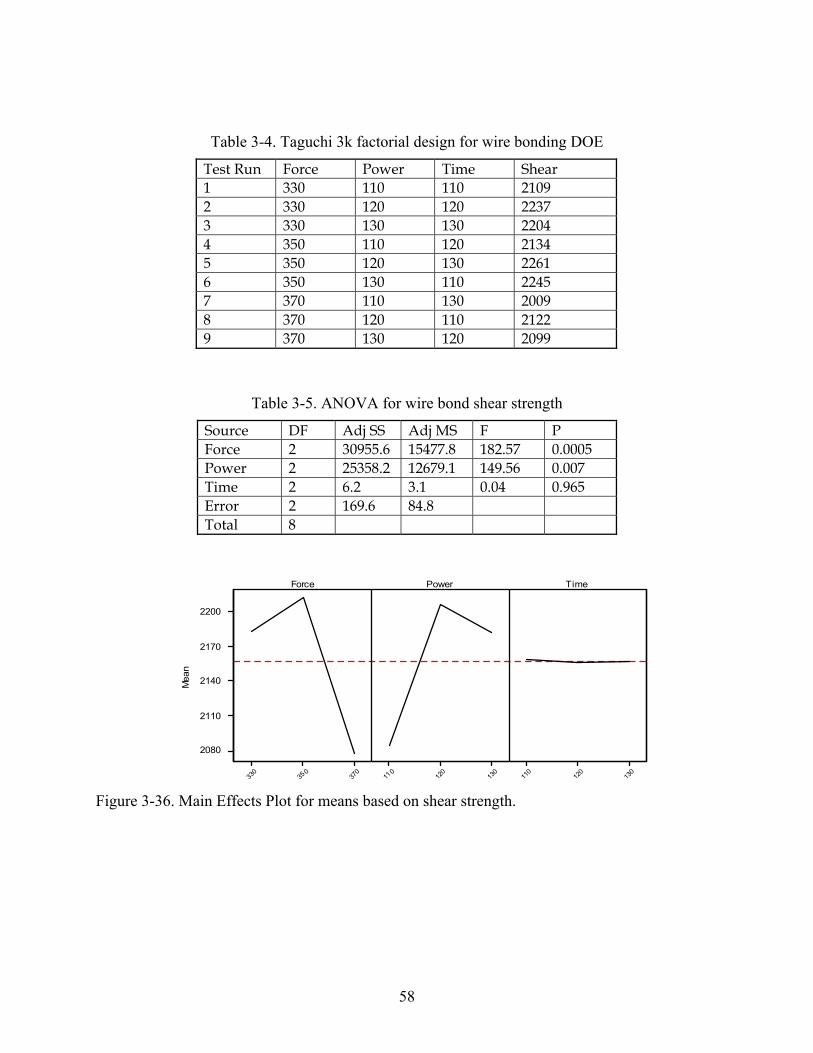
58
Table 3-4. Taguchi 3k factorial design for wire bonding DOE
Test Run Force Power Time Shear 1 330 110 110 2109 2 330 120 120 2237 3 330 130 130 2204 4 350 110 120 2134 5 350 120 130 2261 6 350 130 110 2245 7 370 110 130 2009 8 370 120 110 2122 9 370 130 120 2099
Table 3-5. ANOVA for wire bond shear strength
Source DF Adj SS Adj MS F P Force 2 30955.6 15477.8 182.57 0.0005 Power 2 25358.2 12679.1 149.56 0.007 Time 2 6.2 3.1 0.04 0.965 Error 2 169.6 84.8 Total 8
TimePowerForce
130
120
110
130
120
110
370
350
330
2200
2170
2140
2110
2080
Mea
n
Figure 3-36. Main Effects Plot for means based on shear strength.

59
Table 3-6. Optimal wire bonding parameters for thick gold substrate
Gold Platinum Force (g-f) 350 450
Power 1 (µinch) 120 130 Power 2 (µinch) 125 135 Time 1 (µsec) 120 110 Time 2 (µsec) 120 110
Predelay Time (µsec) 100 100 Temperature (ºC) 225 250
Accelerated Aging Tests Accelerated aging was performed on the wire bonds to examine the effect of aging on the strength of the wire bonds. The accelerated aging was performed in a Blue MOV-18C oven at 350°C for 0, 100, 250, 500, 1000 and 2000 hours. Figures 3-37 and 3-38 show the results of the gold and platinum wire bond pull and shear strength testing as a function of aging time performed on the ceramic substrate metallization. Shear1 is the shear strength of the first bond and shear2 is the shear strength of the second bond. The wire loop geometry produced a 45º angle during the pull test. The force applied to the wire (Force (true)) was 0.707 times the measured force (FM). The pull test data reported and plotted is FM. Twenty-four measurements (shears or pulls) were made and averaged per data point.
From Figure 3-37, it can be seen that the average pull and shear strength of the gold wire bonds decreased during the first 100 hours, which was caused by the stress relief by annealing, after which the pull strength remained constant throughout the remainder of the tests. The shear strength increased slightly with increasing aging time and remained approximately constant for long time aging. The gold remnant was 100% and there were no bond lifts during the whole accelerated aging test process.
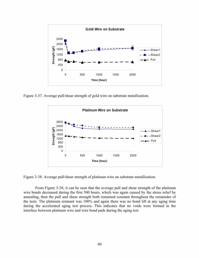
60
Gold Wire on Substrate
0
400
800
1200
1600
2000
2400
0 500 1000 1500 2000
Time (hour)
Stre
ngth
(gF)
Shear1
Shear2Pull
Figure 3-37. Average pull/shear strength of gold wire on substrate metallization.
Platinum Wire on Substrate
0400800
12001600200024002800
0 500 1000 1500 2000
Time (hour)
Stre
ngth
(gF)
Shear1
Shear2Pull
Figure 3-38. Average pull/shear strength of platinum wire on substrate metallization.
From Figure 3-38, it can be seen that the average pull and shear strength of the platinum wire bonds decreased during the first 500 hours, which was again caused by the stress relief by annealing, then the pull and shear strength both remained constant throughout the remainder of the tests. The platinum remnant was 100% and again there was no bond lift at any aging time during the accelerated aging test process. This indicates that no voids were formed in the interface between platinum wire and wire bond pads during the aging test.
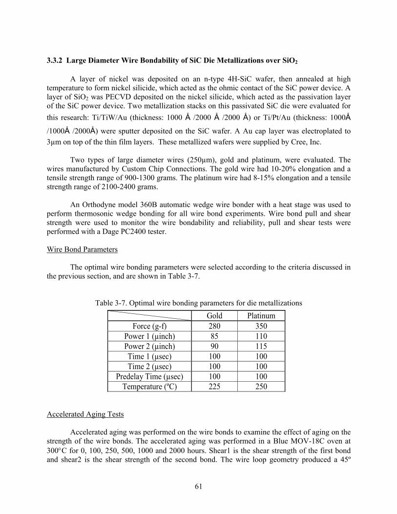
61
3.3.2 Large Diameter Wire Bondability of SiC Die Metallizations over SiO2
A layer of nickel was deposited on an n-type 4H-SiC wafer, then annealed at high temperature to form nickel silicide, which acted as the ohmic contact of the SiC power device. A layer of SiO2 was PECVD deposited on the nickel silicide, which acted as the passivation layer of the SiC power device. Two metallization stacks on this passivated SiC die were evaluated for this research: Ti/TiW/Au (thickness: 1000 Å /2000 Å /2000 Å) or Ti/Pt/Au (thickness: 1000Å
/1000Å /2000Å) were sputter deposited on the SiC wafer. A Au cap layer was electroplated to 3µm on top of the thin film layers. These metallized wafers were supplied by Cree, Inc. Two types of large diameter wires (250µm), gold and platinum, were evaluated. The wires manufactured by Custom Chip Connections. The gold wire had 10-20% elongation and a tensile strength range of 900-1300 grams. The platinum wire had 8-15% elongation and a tensile strength range of 2100-2400 grams. An Orthodyne model 360B automatic wedge wire bonder with a heat stage was used to perform thermosonic wedge bonding for all wire bond experiments. Wire bond pull and shear strength were used to monitor the wire bondability and reliability, pull and shear tests were performed with a Dage PC2400 tester. Wire Bond Parameters The optimal wire bonding parameters were selected according to the criteria discussed in the previous section, and are shown in Table 3-7.
Table 3-7. Optimal wire bonding parameters for die metallizations
Gold Platinum Force (g-f) 280 350
Power 1 (µinch) 85 110 Power 2 (µinch) 90 115 Time 1 (µsec) 100 100 Time 2 (µsec) 100 100
Predelay Time (µsec) 100 100 Temperature (ºC) 225 250
Accelerated Aging Tests
Accelerated aging was performed on the wire bonds to examine the effect of aging on the strength of the wire bonds. The accelerated aging was performed in a Blue MOV-18C oven at 300°C for 0, 100, 250, 500, 1000 and 2000 hours. Shear1 is the shear strength of the first bond and shear2 is the shear strength of the second bond. The wire loop geometry produced a 45º
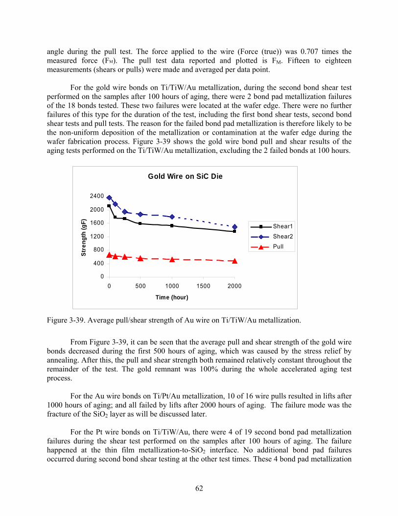
62
angle during the pull test. The force applied to the wire (Force (true)) was 0.707 times the measured force (FM). The pull test data reported and plotted is FM. Fifteen to eighteen measurements (shears or pulls) were made and averaged per data point.
For the gold wire bonds on Ti/TiW/Au metallization, during the second bond shear test
performed on the samples after 100 hours of aging, there were 2 bond pad metallization failures of the 18 bonds tested. These two failures were located at the wafer edge. There were no further failures of this type for the duration of the test, including the first bond shear tests, second bond shear tests and pull tests. The reason for the failed bond pad metallization is therefore likely to be the non-uniform deposition of the metallization or contamination at the wafer edge during the wafer fabrication process. Figure 3-39 shows the gold wire bond pull and shear results of the aging tests performed on the Ti/TiW/Au metallization, excluding the 2 failed bonds at 100 hours.
Gold Wire on SiC Die
0
400
800
1200
1600
2000
2400
0 500 1000 1500 2000
Time (hour)
Stre
ngth
(gF) Shear1
Shear2
Pull
Figure 3-39. Average pull/shear strength of Au wire on Ti/TiW/Au metallization.
From Figure 3-39, it can be seen that the average pull and shear strength of the gold wire
bonds decreased during the first 500 hours of aging, which was caused by the stress relief by annealing. After this, the pull and shear strength both remained relatively constant throughout the remainder of the test. The gold remnant was 100% during the whole accelerated aging test process.
For the Au wire bonds on Ti/Pt/Au metallization, 10 of 16 wire pulls resulted in lifts after 1000 hours of aging; and all failed by lifts after 2000 hours of aging. The failure mode was the fracture of the SiO2 layer as will be discussed later.
For the Pt wire bonds on Ti/TiW/Au, there were 4 of 19 second bond pad metallization failures during the shear test performed on the samples after 100 hours of aging. The failure happened at the thin film metallization-to-SiO2 interface. No additional bond pad failures occurred during second bond shear testing at the other test times. These 4 bond pad metallization
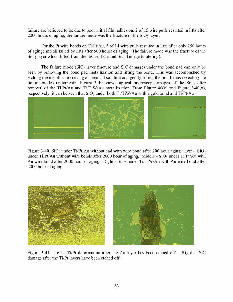
63
failure are believed to be due to poor initial film adhesion. 2 of 15 wire pulls resulted in lifts after 2000 hours of aging; the failure mode was the fracture of the SiO2 layer.
For the Pt wire bonds on Ti/Pt/Au, 5 of 14 wire pulls resulted in lifts after only 250 hours
of aging; and all failed by lifts after 500 hours of aging. The failure mode was the fracture of the SiO2 layer which lifted from the SiC surface and SiC damage (cratering).
The failure mode (SiO2 layer fracture and SiC damage) under the bond pad can only be seen by removing the bond pad metallization and lifting the bond. This was accomplished by etching the metallization using a chemical solution and gently lifting the bond, thus revealing the failure modes underneath. Figure 3-40 shows optical microscope images of the SiO2 after removal of the Ti/Pt/Au and Ti/TiW/Au metallization. From Figure 40(c) and Figure 3-40(a), respectively, it can be seen that SiO2 under both Ti/TiW/Au with a gold bond and Ti/Pt/Au
Figure 3-40. SiO2 under Ti/Pt/Au without and with wire bond after 200 hour aging. Left - SiO2 under Ti/Pt/Au without wire bonds after 2000 hour of aging. Middle - SiO2 under Ti/Pt/Au with Au wire bond after 2000 hour of aging. Right - SiO2 under Ti/TiW/Au with Au wire bond after 2000 hour of aging.
Figure 3-41. Left - Ti/Pt deformation after the Au layer has been etched off. Right - SiC damage after the Ti/Pt layers have been etched off.
64
without a wire bond were intact after 2000 hours of aging at 300°C, while SiO2 under Ti/Pt/Au with a gold bond showed fractures after 2000 hours of aging at 300°C [Figure 3-40(b)]. Another failure mode was SiC damage as shown in Fig. 3-41. This SiC damage failure mode only occurred for platinum wire bonding on Ti/Pt/Au metallization. Failure Analysis
Compared to fine wire bonding, much higher bond force is required in the large diameter wedge bonding process. Cratering has been observed in both Al ultrasonic and Au thermosonic bonding at high bonding force in silicon devices. High bonding force coupled with ultrasonic energy may cause craters in the silicon, particularly if there is any localized stress concentration. In some cases, particularly in Al wedge bonding, even low bond forces seem to cause cratering. Bond pad metallization materials and structures affect bondability as well as bond reliability. It has been observed from experiments that as the metallization thickness increases there is a significant reduction in the cratering failure mode during shear test. It has also been experimentally shown that thinner metallization has a higher tendency for cratering than thicker metal. This has been attributed to the “cushioning effect” of the thicker metal.
In this work, gold wire had better reliability results on SiO2 over SiC than platinum wire based on a comparison of the failure start times and failure modes for the same metallization. Higher bonding force and ultrasonic energy levels were required for platinum wire bonding because the platinum wire has higher hardness than gold wire. Ti/TiW/Au metallization produced better aging test results than the Ti/Pt/Au metallization based on a comparison of the failure start times and failure modes. The differences between the two types of metallization were TiW versus Pt as well as their thickness. Therefore the metallization structure is likely to contribute to the different reliabilities.
A complete understanding of the effect of bonding force and bonding pad metallization
structure is necessary in order to explain wire bonding failures such as cratering, peeling and cracking. In reality, wire bonding is a complicated, multi-physics, transient dynamic process, which is completed within a very short time. The bond pad thickness normally is only a few microns. It is almost impossible to directly measure the strains or stresses experimentally. Hence, a simplified finite element model (FEM) was performed to understand the effect of bonding force and bond pad metallization on the failure mode, and may further help to improve the bonding process and bond pad metallization design by avoiding die failure modes, such as SiO2 fracture and SiC damage.

65
Figure 3-42. Bond head movement (Orthodyne 360B Operating Manual).
For FEM success, the bonding process, especially the bond head movement must be clearly understood. Figure 3-42 shows the bond head movement of the Orthodyne bonder used in this research.
At the beginning of the wire bonding process, the bond head moves from home over and
down to a position above the bond point. The position above the bond point is “search”. The bond head reaches the design velocity limit while traversing half the distance, then decreases to zero velocity at the search position.
At search, the velocity of the bonding tool is reduced to allow the head to move down to
the wire surface gently and slowly so as not to flatten the wire when the tool makes contact with the surface. The bond head positions the tool at a height above the work surface (search height) before continuing down at a slow constant velocity (search to bond pad).
Before the head moves down from the search height toward the bond pad, the
programmed bonding force is fully applied to the transducer at search height. The head continues down until the touch down switch opens indicating the tool and wire touched the work surface. A programmed prebond delay period 100msec is applied to assure that the head has come to a complete stop before beginning the bonding process. Then, ultrasonic bonding power is applied to the transducer to begin the bonding process. During this period, the head moves down beyond the point where the touch down switch opened to provide a small vertical distance for the tool to lower as it flattens the wire during bonding.
Bonding force (gram force) is the static load applied downward against the wire. And
the initial touch down contact area is very small in order to obtain 100% bonded area. A high
Bond tool
(a) Home (c) Touch down (b) Search
Initial contact Bond Pad
Large bond area
(d) Overtravel
Search height

66
bonding force is required for the large diameter wire bonding. Thus, a high pressure focuses on the touch down area.
Ansys 9.0 software was used to carry out the simulation in this study. The construction of
a finite element model includes a consideration of the material properties, the geometry and mesh, and the loading. In addition, the careful selection of the element type is also essential due to its effect on the simulation accuracy. A summary of the material properties used in the simulation is shown in Table 3-8. Several assumptions were specified in this simulation: 1) all the materials are linear elastic; 2) temperature in the metallization is uniformly distributed; 3) Young’s modulus of all the materials do not change with the application of ultrasonic energy; and 3) there are no contact intermetallic effect and diffusion in the bond formation.
A simplified 2D model was established according to the previous description of the
bond head movement. The 2D model is shown in Figure 3-43, which is cut from a die with 3 layer metallization Ti/TiW/Au (thickness: 1000Å/2000Å /3µm) and SiO2 layer (thickness: 1000Å) above the SiC (thickness: 10µm). It is noted that the real thickness of SiC was about 400µm. 10µm thickness was used in the model to save calculation time. The bottom of the SiC was fixed and the two sides were constrained in the horizontal direction. Figure 3-44 gives the meshes and load on the bond pad metallization. The bonding force was replaced by pressure on a line, the length of the line equaled to the initial wire touch down width, and
Table 3-8. Materials properties at 225/250ºC (references 3.2 – 3.5)
0.21 430 4.5 SiC
0.23 165 0.4 SiO2
0.32 102 8.6 Ti
0.28 407 4.5~5.8 TiW
0.38 157 8.8 Pt
0.44 73 14.2 Au
Poisson Ratio Young's Modulus (/GPa)
Thermal Expansion Coefficient (10-6/K)

67
Figure 3-43. Bond pad metallization 2D model. the pressure equaled to the bonding force over the initial wire touch down area. The initial touchdown width was selected as 2µm, the area is about 2 µm x 420µm; the bonding force for gold wire was 280 g-f, and for platinum wire was 350 g-f. In this 2D model, the geometry unit used was nm, the corresponded pressure for Au wire was 3.3E-7 g/nm2, and for Pt wire was 4.2E-7 g/nm2. The simulation temperature used for Au wire bonding was 225ºC, Pt wire bonding was 250ºC.
Figures 3-45 through 3-52 show the simulation results of Von Mises stress and strain in the bond pad metallizations for Au and Pt wire bonding. Table 3-9 shows the comparison between the FEMA simulation results and experimentally testing results.
SiC (10µm) SiO2 (1000Å)
Ti (1000Å)
Au (3µm)
TiW (2000Å)
10µm
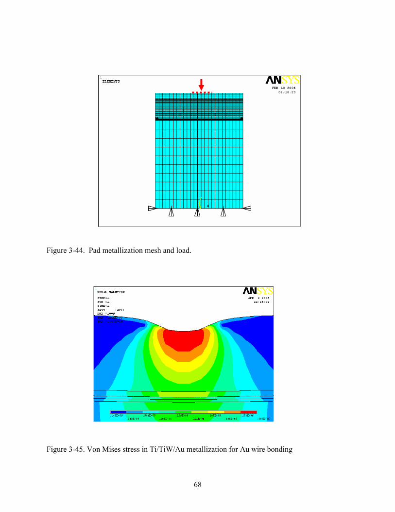
68
Figure 3-44. Pad metallization mesh and load.
Figure 3-45. Von Mises stress in Ti/TiW/Au metallization for Au wire bonding

69
Figure 3-46. Von Mises strain in Ti/TiW/Au metallization for Au wire bonding.
Figure 3-47. Von Mises stress in Ti/Pt/Au metallization for Au wire bonding.
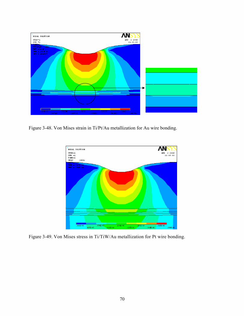
70
Figure 3-48. Von Mises strain in Ti/Pt/Au metallization for Au wire bonding.
Figure 3-49. Von Mises stress in Ti/TiW/Au metallization for Pt wire bonding.

71
Figure 3-50. Von Mises strain in Ti/TiW/Au metallization for Pt wire bonding.
Figure 3-51. Von Mises stress in Ti/Pt/Au metallization for Pt wire bonding.
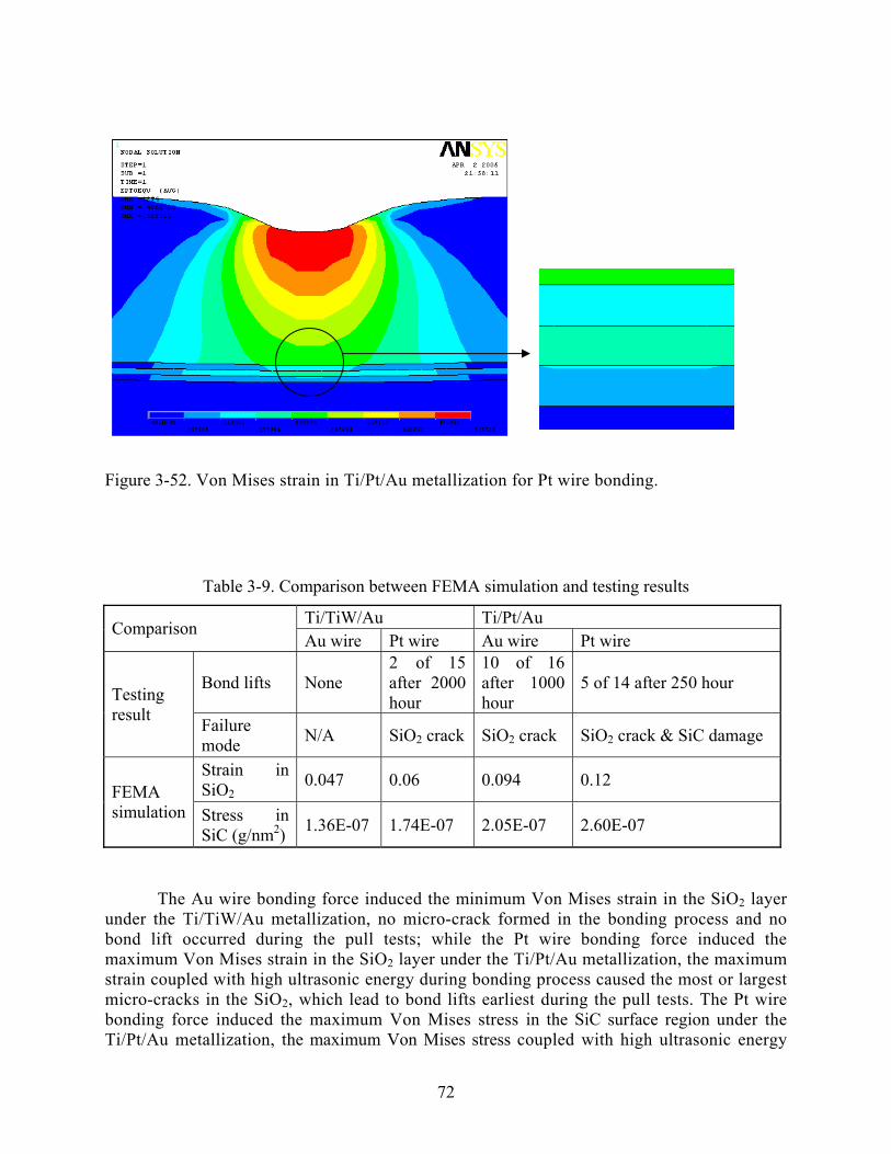
72
Figure 3-52. Von Mises strain in Ti/Pt/Au metallization for Pt wire bonding.
Table 3-9. Comparison between FEMA simulation and testing results
Ti/TiW/Au Ti/Pt/Au Comparison Au wire Pt wire Au wire Pt wire
Bond lifts None 2 of 15 after 2000 hour
10 of 16 after 1000 hour
5 of 14 after 250 hour Testing result Failure
mode N/A SiO2 crack SiO2 crack SiO2 crack & SiC damage
Strain in SiO2
0.047 0.06 0.094 0.12 FEMA simulation Stress in
SiC (g/nm2) 1.36E-07 1.74E-07 2.05E-07 2.60E-07
The Au wire bonding force induced the minimum Von Mises strain in the SiO2 layer under the Ti/TiW/Au metallization, no micro-crack formed in the bonding process and no bond lift occurred during the pull tests; while the Pt wire bonding force induced the maximum Von Mises strain in the SiO2 layer under the Ti/Pt/Au metallization, the maximum strain coupled with high ultrasonic energy during bonding process caused the most or largest micro-cracks in the SiO2, which lead to bond lifts earliest during the pull tests. The Pt wire bonding force induced the maximum Von Mises stress in the SiC surface region under the Ti/Pt/Au metallization, the maximum Von Mises stress coupled with high ultrasonic energy
73
during bonding process caused SiC damage. The FEMA simulation results correlated with the testing results very well.
3.3.3 Large Diameter Wire Bondability of SiC Die Metallization without SiO2 A innovate composite contact metallization composite on SiC for high temperature applications has been developed by Auburn University researchers in the Physics Department. The metallization stack Ta-Si-N (2%)/Pt-N/Au (thickness: 1500Å /1000Å /3µm) deposited on nickel silicides on a SiC wafer using a hot sputtering technique was proven to have high stability at a high temperature of 350ºC. This work was to investigate the wire bonding reliability of this metallization stack.
The metallization stack Ta-Si-N (2%)/Pt-N/Au on nickel silicide ohmic contact on SiC wafer was fabricated as follows:
• Pre-Clean SiC wafer in organic and inorganic solution. • High vacuum sputter the Ni (thickness < 800 Å) on the SiC wafer. • Anneal at 900°C for 1 minute in a high vacuum chamber (10-6 torr) to form Ni2Si as
ohmic contact. • Load SiC wafer on the back-heated wafer holder in a three target high vacuum
sputtering chamber. • Pump vacuum to 10-7 torr. • Vent Ar/N2 (2%) gas mixture into the chamber. • Sputter TaSi2 on to the SiC wafter. • Heat to 250ºC, and sputter Pt on to the SiC wafer. • Sputter Au on to the SiC wafer at temperature of less than 150ºC. • Electroplate Au to a thickness of 3µm. • Dice the wafer to the experimental size (1inch x1inch).
Large diameter gold wire (250µm) manufactured by Custom Chip Connections was used again in this work. The wire loop geometry produced a 45º angle during the pull test. The force applied to the wire (Force (true)) was 0.707 times the measured force (FM). The pull test data reported and plotted is FM. 16 measurements (shears or pulls) were made and averaged per data point. Accelerated Aging Tests Accelerated aging was performed on the wire bonds to evaluate the wire bond reliability with this metallization stack. The accelerated aging was performed in a Blue MOV-18C oven at 350°C for 0, 100, 250, 500, 1000 and 2000 hours. Figure 3-53 shows the gold wire bond pull and shear results for the accelerated aging tests performed on the metallization, shear1 is the shear strength of the first bond and shear 2 is the shear strength of the second bond. From the figure, it can be seen that this metallization stack Ta-Si-N (2%)/Pt-N/Au had good reliability with gold wire bond for applications at 350ºC.

74
Strength vs. Aging time
500
1000
1500
2000
2500
0 500 1000 1500 2000
Aging time (hour)
Stre
ngth
(gF)
Shear1Shear2Pull
Figure 3-53. Average shear/pull strength of gold wire bonds on Ta-Si-N 92%)/Pt-N/Au.
3.3.4 Conclusions Large diameter (250µm) gold and platinum wires have good bondability on ceramic substrate thick metallization and high reliability with 350ºC aging. Platinum wire bond has higher strength than gold wire.
For SiC/Ni2Si/SiO2/Ti/TiW/Au metallization, Au wire bonds had good reliability with 300ºC aging, while 2 of 15 Pt wire bonds had bond lifts during pull testing after 2000 hours of aging. For SiC/Ni2Si/SiO2/Ti/Pt/Au metallization, 10 of 16 Au wire bonds had bond lifts during pull testing after 1000 hours of aging, 5 of 14 Pt wire bonds had bond lifts during pull testing after 250 hours of aging.
A simplified FEMA 2D model was used to understand the effects of bond force and die
metallization structure on the failure mode. The results matched the experimental results very well. The best combination was Au wire on a Ti/TiW/Au pad stack over PECVD SiO2. This work demonstrated the effects of wire and pad metallurgy on bond reliability.
The metallization stack Ta-Si-N (2%)/Pt-N/Au had good reliability with gold wire bonds
for applications at 350ºC. More work needs to be done to investigate the reliability of this metal system for applications at higher temperatures. 3.4 Characterization of High Temperature Electrical Insulation Polymers
Devices operating under high power conditions may also be exposed to high voltages, and as a result high voltage breakdown may occur between adjacent electrical connections. To prevent this, an effective dielectric passivation coating must be applied to ensure reliable package operation.

75
3.4.1 Polyimide Dupont PI2611 polyimide has an exceptional combination of high thermal stability, good
mechanical toughness, good chemical corrosion resistance, excellent dielectric properties and relatively low moisture uptake due to its rodlike structure with a backbone composed of rigid cyclic elements. It can be used as a passivation material to decrease the leakage current and increase the breakdown voltage between adjacent ohmnic contact pads. Test Sample Fabrication and Experiment Set-up
In this research, Dupont PI2611 polyimide coated on quartz substrates (2 x 1 x 0.040 inch) was evaluated for its breakdown strength at high temperature. The test pattern was designed as shown in Figure 3-54: two 25µm wide, 3mm long metal traces were paralleled with 100µm spacing, and two 1mm x 1mm probe pads were spaced 2cm apart. The metal traces were sputtered Cr/Au (thickness: 1000Å /2000Å) thin film; the polyimide material covered only the two parallel traces, the thickness was about 6-9µm. The polyimide test sample fabrication was as follows:
• Pre-Clean quartz substrate in organic and inorganic solution. • Spin apply negative photoresist on the substrate, and soft-bake at 105ºC on a hot plate
for 60 seconds. • Pattern test circuit on the substrate by UV Exposure using Kurl Sauss MA6. • Remove exposed photoresist by developer. • Hard-bake the substrate at 120C on a hot plate for 60 seconds. • High vacuum E-beam deposite Cr/Au (thickness: 1000 Å /2000 Å) on the substrates. • Strip photoresist by Acetone solution. • Spin apply adhesion promoter on the substrate, and soft-bake at 150°C on a hot plate
for 90 seconds. • Manually dispense the polyimide PI2611 to cover the test circuit with a syringe. • Soft-bake polyimide film at 90°C and then 150°C on separate hot plates for 90
seconds each. • Load the substrates into the programmable oven SST 3150. • Ramp to 150°C in Nitrogen at a rate of 10°C/Min. • Ramp to 350°C in Nitrogen at a rate of 4°C/Min, and cure for 30 minutes at 350°C
(the curing profile is shown in Figure 55). • Cool down to ambient.
After the samples were fabricated, as-built and aged samples (100, 250, 500, 1000 and 2000 hours at 300oC in an air chamber) were tested using a high temperature probe station. (The parts were not biased during high temperature storage.) The two contact pads were connected to a computer controlled power supply and a current meter using special probes and cables.
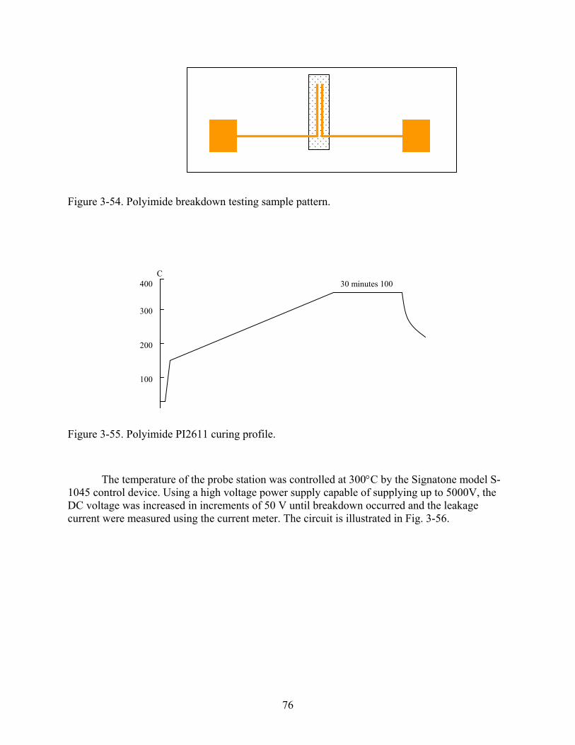
76
Figure 3-54. Polyimide breakdown testing sample pattern.
100
C 30 minutes 100
200
300
400
Figure 3-55. Polyimide PI2611 curing profile. The temperature of the probe station was controlled at 300°C by the Signatone model S-1045 control device. Using a high voltage power supply capable of supplying up to 5000V, the DC voltage was increased in increments of 50 V until breakdown occurred and the leakage current were measured using the current meter. The circuit is illustrated in Fig. 3-56.
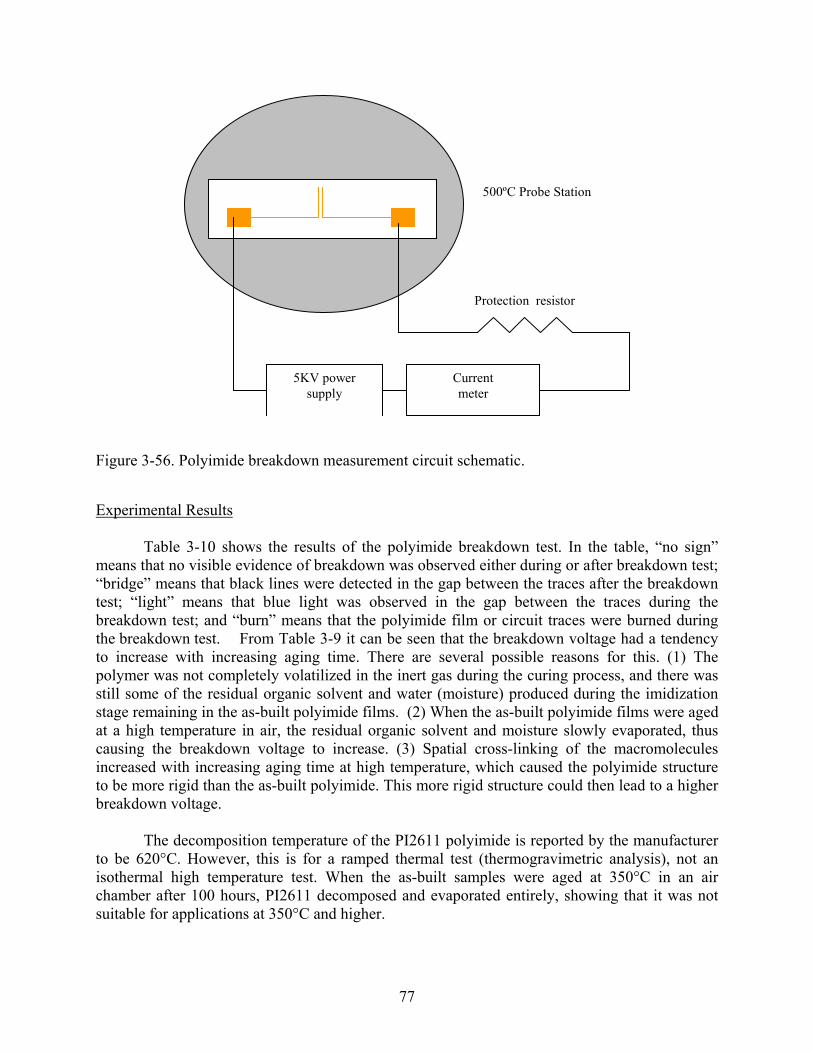
77
5KV power supply
Current meter
Protection resistor
500ºC Probe Station
Figure 3-56. Polyimide breakdown measurement circuit schematic.
Experimental Results Table 3-10 shows the results of the polyimide breakdown test. In the table, “no sign” means that no visible evidence of breakdown was observed either during or after breakdown test; “bridge” means that black lines were detected in the gap between the traces after the breakdown test; “light” means that blue light was observed in the gap between the traces during the breakdown test; and “burn” means that the polyimide film or circuit traces were burned during the breakdown test. From Table 3-9 it can be seen that the breakdown voltage had a tendency to increase with increasing aging time. There are several possible reasons for this. (1) The polymer was not completely volatilized in the inert gas during the curing process, and there was still some of the residual organic solvent and water (moisture) produced during the imidization stage remaining in the as-built polyimide films. (2) When the as-built polyimide films were aged at a high temperature in air, the residual organic solvent and moisture slowly evaporated, thus causing the breakdown voltage to increase. (3) Spatial cross-linking of the macromolecules increased with increasing aging time at high temperature, which caused the polyimide structure to be more rigid than the as-built polyimide. This more rigid structure could then lead to a higher breakdown voltage. The decomposition temperature of the PI2611 polyimide is reported by the manufacturer to be 620°C. However, this is for a ramped thermal test (thermogravimetric analysis), not an isothermal high temperature test. When the as-built samples were aged at 350°C in an air chamber after 100 hours, PI2611 decomposed and evaporated entirely, showing that it was not suitable for applications at 350°C and higher.

78
Table 3-10. Polyimide breakdown test results
3.4.2 Modified Polyimide PI2611 (studied in previous section) was modified by adding nanoreinforced polyhedral oligomeric silsesquioxanes (POSS) supplied by Hybrid Plastics, Inc. (http://www.hybridplastics.com). Upon exposure to oxygen, the POSS polyimide generates a nanoscopically thin glassy layer on the surface, providing a barrier to further oxidation and improves the surface for adhesion and bonding. Two variations of PI2611 were characterized, one with 5 wt% and the other with 10 wt% POSS additive. VM-652 is a solution of organosilane and was used to improve the adhesion of the PI2611 coatings to the quartz test substrate. For VM-652 application, a puddle of VM-652 was allowed to stand on the assembly for 20 seconds,
0 100hr Sample
Breakdown (volt) Leakage (amp) Breakdown (volt) Leakage (amp)
1 3450 no sign 3950 no sign 2 3500 bridge 3825 light 3 3700 light 3575 bridge 4 3475 bridge 3450 bridge 5 3425 bridge
250hr 500hr Sample
Breakdown (volt) Leakage (amp) Breakdown (volt) Leakage (amp)
1 4425 burn 4620 burn 2 4800 light 4550 burn 3 over 5000 4.20E-06 4730 burn 4 over 5000 2~20E-08 4900 light 5 over 5000 2~20E-08 over 5000 3.00E-08 6 over 5000 2~20E-08 over 5000 1.20E-07
1000hr 2000hr Sample
Breakdown (volt) Leakage (amp) Breakdown (volt) Leakage (amp)
1 over 5000 5.00E-05 over 5000 3.00E-03 2 over 5000 5.00E-05 over 5000 2.00E-03 3 over 5000 1.00E-08 over 5000 4-16E-08 4 over 5000 1.00E-08 over 5000 4-16E-08 5 over 5000 1.00E-08 over 5000 4-16E-08 6 over 5000 1.00E-08 over 5000 4-16E-08
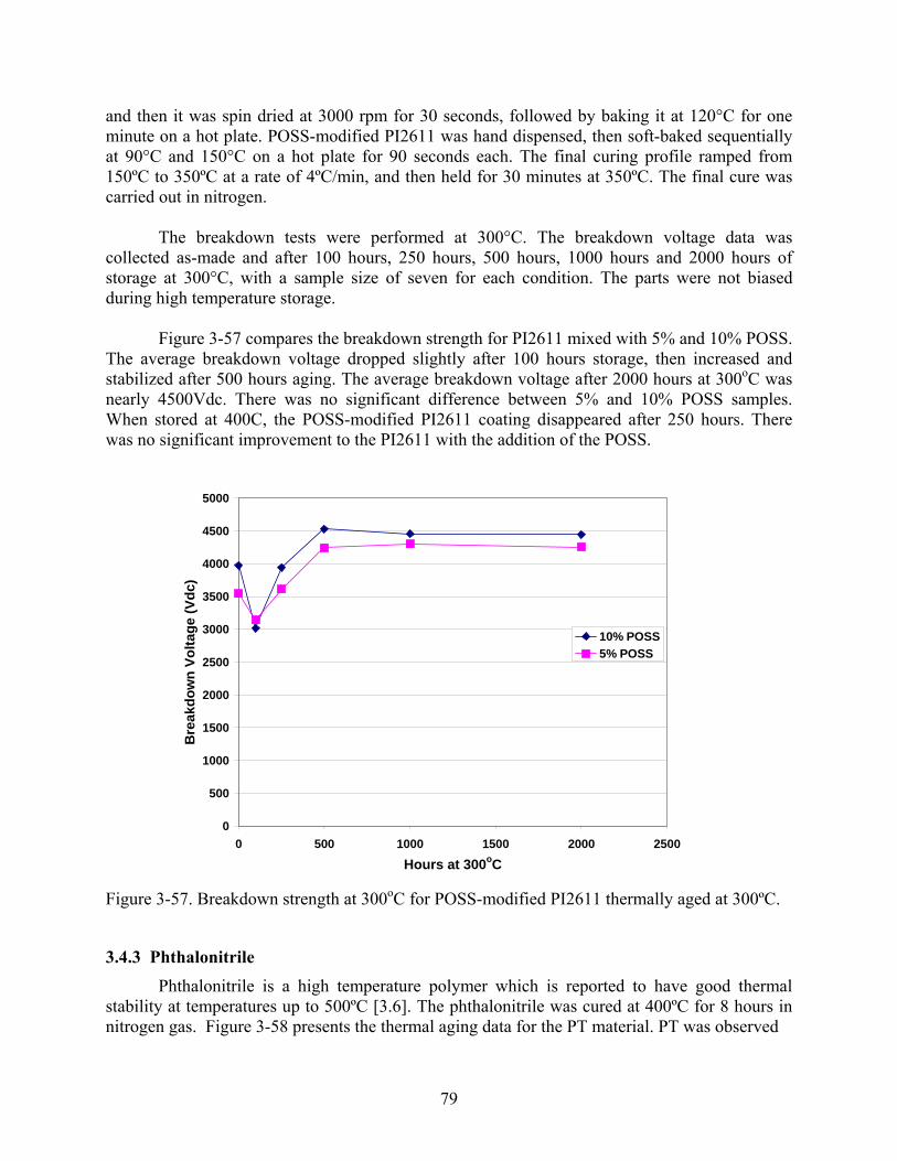
79
and then it was spin dried at 3000 rpm for 30 seconds, followed by baking it at 120°C for one minute on a hot plate. POSS-modified PI2611 was hand dispensed, then soft-baked sequentially at 90°C and 150°C on a hot plate for 90 seconds each. The final curing profile ramped from 150ºC to 350ºC at a rate of 4ºC/min, and then held for 30 minutes at 350ºC. The final cure was carried out in nitrogen.
The breakdown tests were performed at 300°C. The breakdown voltage data was collected as-made and after 100 hours, 250 hours, 500 hours, 1000 hours and 2000 hours of storage at 300°C, with a sample size of seven for each condition. The parts were not biased during high temperature storage.
Figure 3-57 compares the breakdown strength for PI2611 mixed with 5% and 10% POSS.
The average breakdown voltage dropped slightly after 100 hours storage, then increased and stabilized after 500 hours aging. The average breakdown voltage after 2000 hours at 300oC was nearly 4500Vdc. There was no significant difference between 5% and 10% POSS samples. When stored at 400C, the POSS-modified PI2611 coating disappeared after 250 hours. There was no significant improvement to the PI2611 with the addition of the POSS.
0
500
1000
1500
2000
2500
3000
3500
4000
4500
5000
0 500 1000 1500 2000 2500
Hours at 300oC
Bre
akdo
wn
Volta
ge (V
dc)
10% POSS5% POSS
Figure 3-57. Breakdown strength at 300oC for POSS-modified PI2611 thermally aged at 300ºC.
3.4.3 Phthalonitrile Phthalonitrile is a high temperature polymer which is reported to have good thermal stability at temperatures up to 500ºC [3.6]. The phthalonitrile was cured at 400ºC for 8 hours in nitrogen gas. Figure 3-58 presents the thermal aging data for the PT material. PT was observed
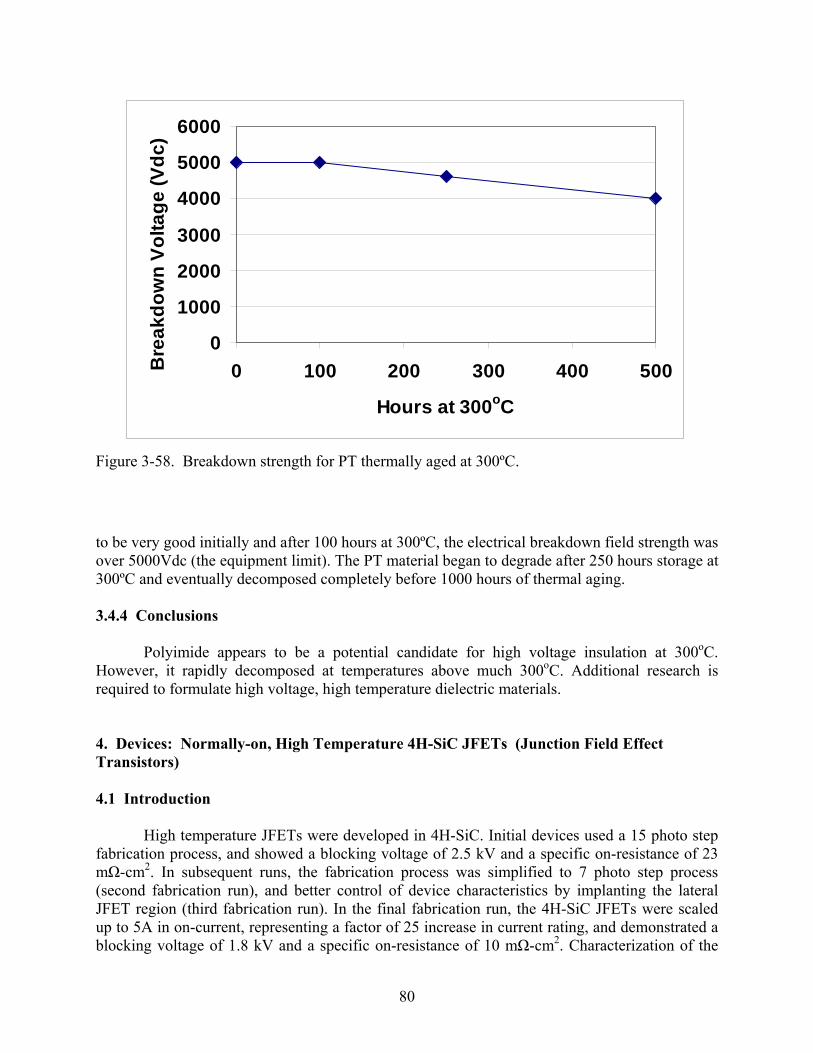
80
0
1000
2000
3000
4000
5000
6000
0 100 200 300 400 500
Hours at 300oC
Bre
akdo
wn
Volta
ge (V
dc)
Figure 3-58. Breakdown strength for PT thermally aged at 300ºC. to be very good initially and after 100 hours at 300ºC, the electrical breakdown field strength was over 5000Vdc (the equipment limit). The PT material began to degrade after 250 hours storage at 300ºC and eventually decomposed completely before 1000 hours of thermal aging. 3.4.4 Conclusions Polyimide appears to be a potential candidate for high voltage insulation at 300oC. However, it rapidly decomposed at temperatures above much 300oC. Additional research is required to formulate high voltage, high temperature dielectric materials. 4. Devices: Normally-on, High Temperature 4H-SiC JFETs (Junction Field Effect Transistors) 4.1 Introduction
High temperature JFETs were developed in 4H-SiC. Initial devices used a 15 photo step fabrication process, and showed a blocking voltage of 2.5 kV and a specific on-resistance of 23 mΩ-cm2. In subsequent runs, the fabrication process was simplified to 7 photo step process (second fabrication run), and better control of device characteristics by implanting the lateral JFET region (third fabrication run). In the final fabrication run, the 4H-SiC JFETs were scaled up to 5A in on-current, representing a factor of 25 increase in current rating, and demonstrated a blocking voltage of 1.8 kV and a specific on-resistance of 10 mΩ-cm2. Characterization of the
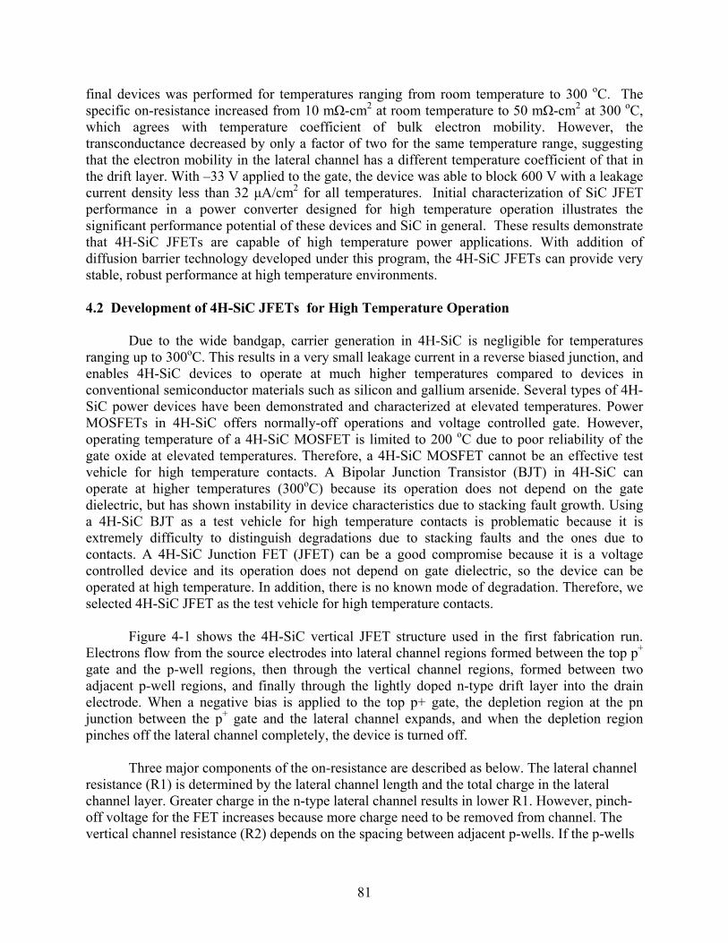
81
final devices was performed for temperatures ranging from room temperature to 300 oC. The specific on-resistance increased from 10 mΩ-cm2 at room temperature to 50 mΩ-cm2 at 300 oC, which agrees with temperature coefficient of bulk electron mobility. However, the transconductance decreased by only a factor of two for the same temperature range, suggesting that the electron mobility in the lateral channel has a different temperature coefficient of that in the drift layer. With –33 V applied to the gate, the device was able to block 600 V with a leakage current density less than 32 μA/cm2 for all temperatures. Initial characterization of SiC JFET performance in a power converter designed for high temperature operation illustrates the significant performance potential of these devices and SiC in general. These results demonstrate that 4H-SiC JFETs are capable of high temperature power applications. With addition of diffusion barrier technology developed under this program, the 4H-SiC JFETs can provide very stable, robust performance at high temperature environments. 4.2 Development of 4H-SiC JFETs for High Temperature Operation
Due to the wide bandgap, carrier generation in 4H-SiC is negligible for temperatures ranging up to 300oC. This results in a very small leakage current in a reverse biased junction, and enables 4H-SiC devices to operate at much higher temperatures compared to devices in conventional semiconductor materials such as silicon and gallium arsenide. Several types of 4H-SiC power devices have been demonstrated and characterized at elevated temperatures. Power MOSFETs in 4H-SiC offers normally-off operations and voltage controlled gate. However, operating temperature of a 4H-SiC MOSFET is limited to 200 oC due to poor reliability of the gate oxide at elevated temperatures. Therefore, a 4H-SiC MOSFET cannot be an effective test vehicle for high temperature contacts. A Bipolar Junction Transistor (BJT) in 4H-SiC can operate at higher temperatures (300oC) because its operation does not depend on the gate dielectric, but has shown instability in device characteristics due to stacking fault growth. Using a 4H-SiC BJT as a test vehicle for high temperature contacts is problematic because it is extremely difficulty to distinguish degradations due to stacking faults and the ones due to contacts. A 4H-SiC Junction FET (JFET) can be a good compromise because it is a voltage controlled device and its operation does not depend on gate dielectric, so the device can be operated at high temperature. In addition, there is no known mode of degradation. Therefore, we selected 4H-SiC JFET as the test vehicle for high temperature contacts.
Figure 4-1 shows the 4H-SiC vertical JFET structure used in the first fabrication run.
Electrons flow from the source electrodes into lateral channel regions formed between the top p+ gate and the p-well regions, then through the vertical channel regions, formed between two adjacent p-well regions, and finally through the lightly doped n-type drift layer into the drain electrode. When a negative bias is applied to the top p+ gate, the depletion region at the pn junction between the p+ gate and the lateral channel expands, and when the depletion region pinches off the lateral channel completely, the device is turned off.
Three major components of the on-resistance are described as below. The lateral channel
resistance (R1) is determined by the lateral channel length and the total charge in the lateral channel layer. Greater charge in the n-type lateral channel results in lower R1. However, pinch-off voltage for the FET increases because more charge need to be removed from channel. The vertical channel resistance (R2) depends on the spacing between adjacent p-wells. If the p-wells
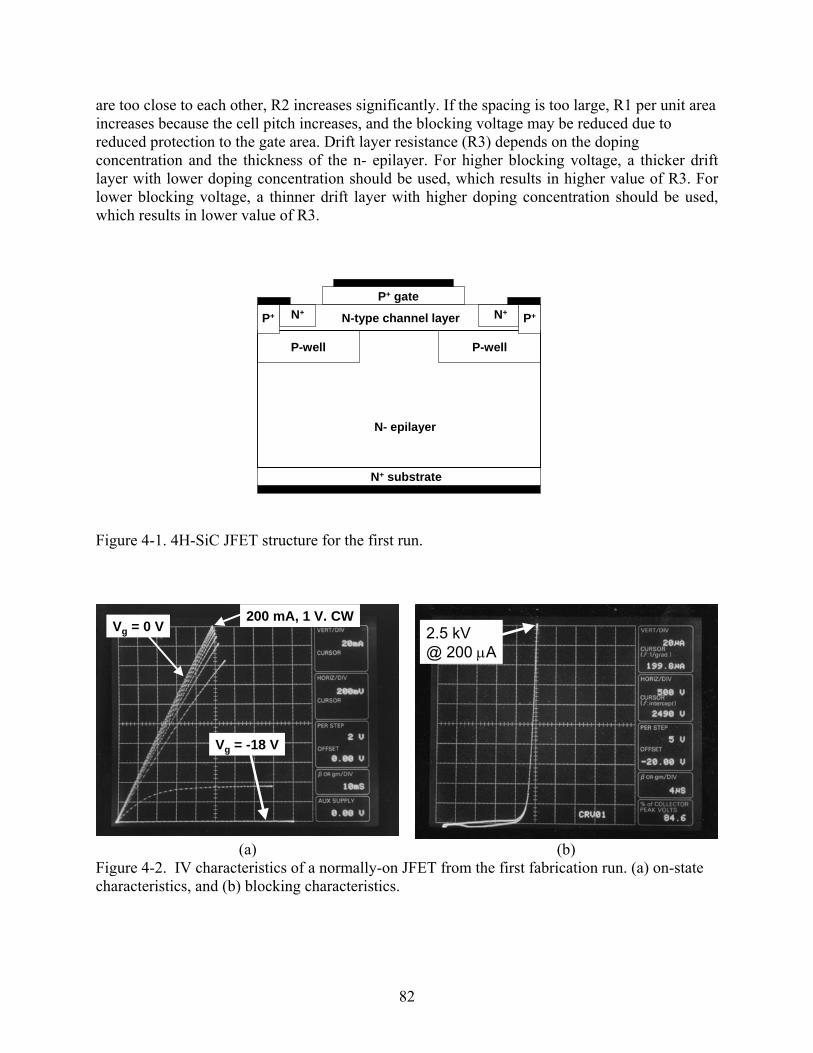
82
are too close to each other, R2 increases significantly. If the spacing is too large, R1 per unit area increases because the cell pitch increases, and the blocking voltage may be reduced due to reduced protection to the gate area. Drift layer resistance (R3) depends on the doping concentration and the thickness of the n- epilayer. For higher blocking voltage, a thicker drift layer with lower doping concentration should be used, which results in higher value of R3. For lower blocking voltage, a thinner drift layer with higher doping concentration should be used, which results in lower value of R3.
Figure 4-1. 4H-SiC JFET structure for the first run.
Vg = 0 V
Vg = -18 V
200 mA, 1 V. CW2.5 kV @ 200 μA
(a) (b) Figure 4-2. IV characteristics of a normally-on JFET from the first fabrication run. (a) on-state characteristics, and (b) blocking characteristics.
N+ N+
P-well P-well
N- epilayer
N-type channel layer
P+ gate
P+ P+
N+ substrate
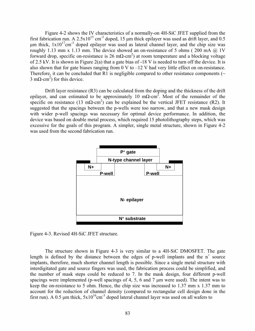
83
Figure 4-2 shows the IV characteristics of a normally-on 4H-SiC JFET supplied from the first fabrication run. A 2.5x1015 cm-3 doped, 15 μm thick epilayer was used as drift layer, and 0.5 μm thick, 1x1017cm-3 doped epilayer was used as lateral channel layer, and the chip size was roughly 1.13 mm x 1.13 mm. The device showed an on-resistance of 5 ohms ( 200 mA @ 1V forward drop, specific on-resistance is 26 mΩ-cm2) at room temperature and a blocking voltage of 2.5 kV. It is shown in Figure 2(a) that a gate bias of -18 V is needed to turn off the device. It is also shown that for gate biases ranging from 0 V to –12 V had very little effect on on-resistance. Therefore, it can be concluded that R1 is negligible compared to other resistance components (~ 3 mΩ-cm2) for this device.
Drift layer resistance (R3) can be calculated from the doping and the thickness of the drift
epilayer, and can estimated to be approximately 10 mΩ-cm2. Most of the remainder of the specific on resistance (13 mΩ-cm2) can be explained be the vertical JFET resistance (R2). It suggested that the spacings between the p-wells were too narrow, and that a new mask design with wider p-well spacings was necessary for optimal device performance. In addition, the device was based on double metal process, which required 15 photolithography steps, which was excessive for the goals of this program. A simpler, single metal structure, shown in Figure 4-2 was used from the second fabrication run.
Figure 4-3. Revised 4H-SiC JFET structure.
The structure shown in Figure 4-3 is very similar to a 4H-SiC DMOSFET. The gate
length is defined by the distance between the edges of p-well implants and the n+ source implants, therefore, much shorter channel length is possible. Since a single metal structure with interdigitated gate and source fingers was used, the fabrication process could be simplified, and the number of mask steps could be reduced to 7. In the mask design, four different p-well spacings were implemented (p-well spacings of 4, 5, 6 and 7 μm were used). The intent was to keep the on-resistance to 5 ohm. Hence, the chip size was increased to 1.37 mm x 1.37 mm to account for the reduction of channel density (compared to rectangular cell design done in the first run). A 0.5 μm thick, 5x1016cm-3 doped lateral channel layer was used on all wafers to
P-well P-well
N- epilayer
N+ substrate
N+ N+
P+ gate
N-type channel layer

84
Figure 4-4. Layout of a JFET device for the second fabrication run. Chip size is 1.37 mm x 1.37 mm.
(a) 4x1015cm-3 (b) 2.5x1015cm-3 (c) 2.0x1015cm-3
Figure 4-5. Blocking characteristics of the 4H-SiC JFETs from the second fabrication run. The Devices had drift epilayers of (a) 4x1015cm-3, (b) 2.5x1015cm-3, and (c) 2.0x1015cm-3. Vgs was –6 V for all measurements. reduce the pinch-off voltage from –18 to –20 V in the first run to around –10 V. Drift layer thickness was fixed at 15 μm, but three different doping concentrations (2x1015 cm-3, 2.5x1015 cm-3, and 4x1015cm-3) were used.
Figure 4-5 shows the blocking characteristics of the JFETs fabricated in the second batch. Due to reduced charge in the lateral channel regions, the pinch-off voltage was also reduced from –20 V to about –3 V. The measurements for the blocking voltage was done in Flourinert Oil, and a gate bias of –6 V was applied to make sure the devices were completely turned off. Devices

85
from all wafers were capable of blocking at least 2.5 kV, with devices with drift layer doping concentration of 2x1015cm-3 supporting 3.0 kV. The difference in p-well spacings did not affect the blocking characteristics.
The reduced pinch-off voltage resulted in lower saturation voltage in the on-state
characteristics. Figure 4-6 shows on-state IV characteristics of two JFETs from a same wafer (with doping concentration of 4x1015cm-3). With 0 V at the gate, the device in Figure 4-6(a) shows saturation characteristics at a Vds of 0.8 V, while the device shown in Figure 4-6(b) saturates at a Vds of around 1.3 V. The resulted in approximately 43% (difference between 230 mA and 330 mA) difference in on-current at a forward drop of 1 V, which is unacceptable for mass production devices. This was due to very small variations in the lateral channel layer thickness and doping concentration.
(a) (b) Figure 4-6. On-state characteristics of JFETs. Both devices came from wafer 6. The p-well spacing was 7 μm.
It is noticeable that the two devices showed almost identical on-resistance when +2 V of gate bias was applied, which reduces the widths of the depletion regions and increases the charge in the lateral channel regions. This indicates that even though it results in higher pinch-off voltage, greater charge in the lateral channel region is preferred because a more uniform, repeatable on-state characteristics can be achieved.
Figure 4-7 shows the effect of p-well spacing on on-current. It is shown that the on-
current does increase with the p-well spacing. With +2 V on the gate, the drain current at a Vds = 1V increased from 444 mA to 518 mA with increasing p-well spacing, which is an increase of 16 %. As shown before, the increase in the p-well spacing does not affect the blocking characteristics. Therefore, use of wider p-well spacing is recommended for future runs.
Figure 4-8 shows the effect of drift layer design on the on-state characteristics. Although
all devices showed acceptable on-state current (both with Vgs = 0 V, and Vgs = + 2 V), the device with thinner drift epilayer with higher doping concentration showed a better characteristics.
Vg = Vg =
Vg = 0
Vg = 0
Vg = - Vg = -

86
Since 2.7 kV or 3.1 kV blocking characteristics are not necessary, the use of 4x1015cm-3 or greater drift epilayer concentration (compared to the first fabrication run) is recommended in the future runs, and the results from this run were presented at 2004 Electronic Materials Conference (EMC04), June, 2004, Notre Dame, IN [4-1].
(a) Id = 444 mA @ Vgs = +2V, Vd = 1V
(b) Id = 475 mA @ Vgs = +2V, Vd = 1V
(c) Id = 483 mA @ Vgs = +2V, Vd = 1V
(d) Id = 518 mA @ Vgs = +2V, Vd = 1V
Figure 4-7. Effect of p-well spacings for on-state characteristics of JFETs. All devices came from a same wafer with a drift layer doping concentration of 4x1015cm-3. The p-well spacings were (a) 4μm, (b) 5μm, (c) 6μm, and (d) 7μm.
In the third 4H-SiC JFET fabrication run, the lateral JFET channel was doped by ion
implantation instead of in-situ doping during the growth of the epilayer. In addition, the total charge in the lateral JFET channel was increased to approximately 1.5x1017 cm-3 (0.5 μm thick) to shift the pinch-off voltage further negative. For more robustness of the device, a polyimide passivation layer was added to the devices. It should be noted that the top metal is Au, and adhesion of polyimide layer on Au is very poor. Therefore, a 500 A thick Ti layer was deposited on top of Au layer to promote adhesion of polyimide. The resulting chip size is 1.070 mm x 1.070 mm, as shown in Figure 4-9.
Vg = 2V Vg = 2V
Vg = 2V Vg = 2V
Vg = 0V
Vg = 0V
Vg = 0V
Vg = 0V
Vg = -2V Vg = -2V
Vg = -2V Vg = -2V

87
Room temperature I-V characteristics are shown in Figure 4-10(a). With a Vgs of 0 V, the device showed an on-current of 330 mA at a forward drop of 1 V. The on-resistance was 3 ohm, where the design goal of this device was 5 ohm (200 mA at a forward drop of 1 V). The pinch-off voltage measured was approximately –14 V. The blocking characteristics were measured with a gate bias of –15 V (Figure 4-10(b)). The high voltage measurements were performed in
(a) 4x1015cm-3 doping conc. (b) 2.5x1015cm-3 doping conc. (c) 2.0x1015cm-3 doping conc.
Figure 4-8. On-state characteristics of the 4H-SiC JFETs from the second fabrication run. The devices had drift epilayers with (a) 4x1015cm-3 doping concentration, (b) 2.5x1015cm-3 doping concentration, and (c) 2.0x1015cm-3 doping concentration. The p-well spacing is 7 μm for all devices.
1070 um
1070
um
Figure 4-9. Layout of a JFET device for the third fabrication run. Chip size is 1.07 mm x 1.07 mm.
Vg = 2V Vg = 2V Vg = 2V
Vg = -2V Vg = -2V Vg = -2V
Vg = 0V Vg = 0V Vg = 0V

88
Vp = -14 V
(a)
VGS = -15 V
(b)
Figure 4-10. (a) on-state, and (b) off-state I-V characteristics of a normally-on 4H-SiC JFET fabricated in the third fabrication run.
fluorinert to prevent arcing in air. The device showed very small leakage current for drain biases up to 2.35 kV, then showed stable avalanche characteristics at around 2.4 kV.
In the fourth fabrication run, the current rating of the 4H-SiC JFET was scaled up to 5A
which is more suitable for actual applications. Figure 4-11 shows the cross-section of the unit cell, and Figure 4-12 shows the layout of the chip. The chip was approximately 2.8 mm x 2.8 mm in size, and the active area of the device was 4.65x10⁻² cm2. Devices were fabricated using a 12 μm thick, 5 x 1015 cm-3 doped n-type epilayer grown on an n+, 4H-SiC substrate. P-wells and floating guard ring edge termination were formed by Al+ implantation, and n+ source regions were then formed by heavy-dose N+ implantations. The channel length, defined by the distance from the edge of the n+ source implant to the edge of the p-well implant, was 1 μm. The implants were activated at 1600 oC in a silicon-rich ambient. A 0.8 μm thick n-type epilayer with a doping concentration of 1.4 x 1017 cm-3 was grown as the lateral channel layer, and an Al+ implantation was done to form top p+ gate layer and annealed at 1600oC. The top p+ gate layer concentration was 1 x 1019 cm-3 and 0.3 μm deep. The p+ implanted layer and n-channel epilayers were then patterned using a dry etching technique down to n+ source and p-well implants. A 0.6 μm thick PECVD field oxide layer was then deposited and densified in dry O2. After opening vias, Al/Ni ohmic contacts [4.2] were formed on the n+ source, the p-wells, and the p+ gates regions, while Ni was used to form backside ohmics. The ohmic contacts were then covered with TaSi2/Pt (Auburn University) or Ta-Ru (Penn State University) diffusion barrier layers to prevent deterioration of ohmic behavior at elevated temperatures. A 2 μm thick Ti/Pt/Au layer was evaporated and lifted-off to form the metal overlayer. Finally, a 0.3 μm thick Si3N4 layer was deposited and patterned for passivation and contact metal oxidation protection.
Figure 13 shows the on-wafer I-V characteristics of a 4H-SiC JFET, with an active area of 4.65x10⁻² cm2, measured at room temperature. Figure 4-13(a) shows the pulsed on-state IV characteristics measured using a Tektronix 371A curve tracer. With a VGS=0 V, an RDS,ON = 0.21
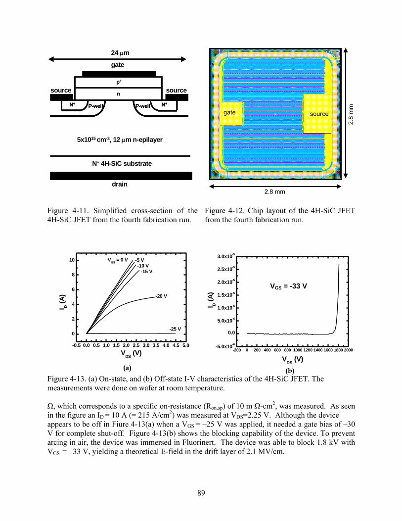
89
Figure 4-11. Simplified cross-section of the 4H-SiC JFET from the fourth fabrication run.
Figure 4-12. Chip layout of the 4H-SiC JFET from the fourth fabrication run.
Figure 4-13. (a) On-state, and (b) Off-state I-V characteristics of the 4H-SiC JFET. The measurements were done on wafer at room temperature. Ω, which corresponds to a specific on-resistance (Ron,sp) of 10 m Ω-cm2, was measured. As seen in the figure an ID = 10 A (= 215 A/cm2) was measured at VDS=2.25 V. Although the device appears to be off in Fiure 4-13(a) when a VGS = –25 V was applied, it needed a gate bias of –30 V for complete shut-off. Figure 4-13(b) shows the blocking capability of the device. To prevent arcing in air, the device was immersed in Fluorinert. The device was able to block 1.8 kV with VGS = –33 V, yielding a theoretical E-field in the drift layer of 2.1 MV/cm.
gate source
2.8
mm
2.8 mm
P-wellN+ P-wellN+
N+ 4H-SiC substrate
5x1015 cm-3, 12 μm n-epilayer
gate
source source
drain
N+P-well N+P-well
24 μm
n
p+
(a) (b)
VGS = -33 V
-0.5 0.0 0.5 1.0 1.5 2.0 2.5 3.0 3.5 4.0 4.5 5.0
0
2
4
6
8
10
-25 V
-20 V
-15 V-10 V
-5 VVGS = 0 V
I D (A)
VDS (V) -200 0 200 400 600 800 1000 1200 1400 1600 1800 2000-5.0x10⁻⁶
0.0
5.0x10⁻⁶
1.0x10⁻⁵
1.5x10⁻⁵
2.0x10⁻⁵
2.5x10⁻⁵
3.0x10⁻⁵
I D (A)
VDS (V)

90
Figure 4-14. On-state I-V characteristics of a 4H-SiC JFET at 300 oC.
Figure 4-15. On-resistance is plotted as a function of temperature. 1/μn is also plotted for comparison.
The devices were brazed to TO-258 packages using Au-Ge eutectic preforms. Fig. 14 shows the on-state IV characteristics of a 4H-SiC JFET at 300 oC. VDS measured at ID = 5 A (107 A/cm2) was approximately 5.7 V. RDS,ON measured at a VDS = 0.2 V and VGS = 0V, increased to 1.07 ohms (Ron,sp = 50 mΩ/cm2), primarily due to a decrease in bulk electron mobility at elevated temperatures. RDS,ON was measured at temperatures ranging from room temperature to 300 oC, and is shown as a function of temperature in Figure 4-15. RDS,ON(T) was compared to calculated values of 1/μn [3]. It can be seen that the on-resistance trend with temperature follows the predicted mobility trend very closely, verifying that the increasing RDS,ON is due to increased drift layer scattering with temperature.
Pinch-off voltage (VP) and transconductance (gm) were also measured as functions of
temperature (Fig. 16). VP was defined as the VGS required to reducing the drain current to <1 μA at VDS = 10 V. At room temperature, a VP = –26.7 V was measured, which increased to –28.9 V at 300 oC. This negative shift in VP is due to an increase in intrinsic carrier concentration (ni) with temperature. Increased ni reduces the built-in potential of the pn junction, which results in a reduction in the width of the depletion region and thus, increasing the amount of charge in the channel. To deplete the additional charge, a more negative bias is required on the gate, translating to a larger magnitude pinch-off voltage. The measurements for gm were done at a VDS = 10 V, and VGS = (VP + 2V), to ensure that the device is in saturation mode. gm is a direct function of the electron mobility in the lateral channel (μn,channel). As expected, the value of gm decreases as the temperature increases. It should be noted that at 300 oC, Ron,sp, which is a function of electron mobility (μn,drift) in the drift layer, increased by a factor of 5, which means that the value of μn,drift was reduced by factor of 5 compared to the value at room temperature. However, gm was reduced by only a factor of two over the same temperature range, which suggests that the temperature dependence of μn,channel is different from that of μn,drift.
-1 0 1 2 3 4 5 6 7 8 9 10
0
1
2
3
4
5
-25 V
-20 V
-15 V-10 V
-5 VVGS = 0 V
I D (A)
VDS (V)0 50 100 150 200 250 300 350
0.2
0.4
0.6
0.8
1.0
1.2
Ron 1/μn
Temperature (oC)
R on (Ω
)
0.001
0.002
0.003
0.004
0.005
0.006
0.007
1/μn (cm
-2Vs)
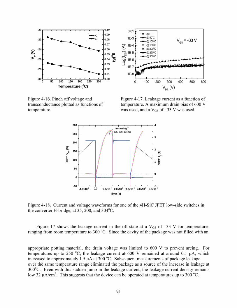
91
Figure 4-16. Pinch off voltage and transconductance plotted as functions of temperature.
Figure 4-17. Leakage current as a function of temperature. A maximum drain bias of 600 V was used, and a VGS of –33 V was used.
Figure 4-18. Current and voltage waveforms for one of the 4H-SiC JFET low-side switches in the converter H-bridge, at 35, 200, and 304oC.
Figure 17 shows the leakage current in the off-state at a VGS of –33 V for temperatures
ranging from room temperature to 300 oC. Since the cavity of the package was not filled with an
appropriate potting material, the drain voltage was limited to 600 V to prevent arcing. For temperatures up to 250 oC, the leakage current at 600 V remained at around 0.1 μA, which increased to approximately 1.5 μA at 300 oC. Subsequent measurements of package leakage over the same temperature range eliminated the package as a source of the increase in leakage at 300oC. Even with this sudden jump in the leakage current, the leakage current density remains low 32 μA/cm2. This suggests that the device can be operated at temperatures up to 300 oC.
0 50 100 150 200 250 300-30
-28
-26
-24
-22
-20
VP gm
Temperature (oC)
V P (V)
0.00
0.01
0.02
0.03
0.04
0.05
0.06
0.07
0.08
0.09
0.10
gm (S)
0 100 200 300 400 500 600
1E-8
1E-7
1E-6
1E-5
1E-4
1E-3
0.01
VDS (V)
VGS = -33 V @ RT @ 500C @ 1000C @ 1500C @ 2000C @ 2500C @ 3000C
Log(
I DS)
(A)
-1.0x10⁻⁵ 0.0 1.0x10⁻⁵ 2.0x10⁻⁵ 3.0x10⁻⁵ 4.0x10⁻⁵ 5.0x10⁻⁵-50
0
50
100
150
200
250
300
-1
0
1
2
3
4
JFET
VD
S (V)
Time (s)
Increasing T(35, 200, 304oC)
JFET
ID (
A)
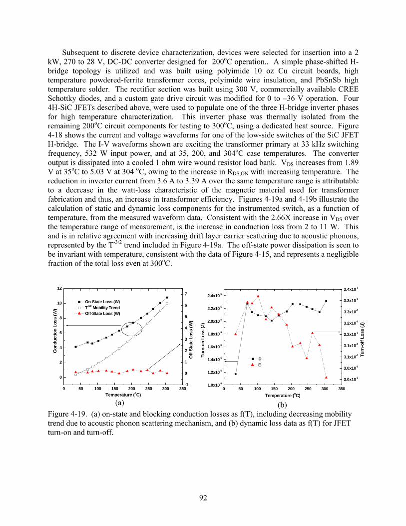
92
Subsequent to discrete device characterization, devices were selected for insertion into a 2 kW, 270 to 28 V, DC-DC converter designed for 200oC operation.. A simple phase-shifted H-bridge topology is utilized and was built using polyimide 10 oz Cu circuit boards, high temperature powdered-ferrite transformer cores, polyimide wire insulation, and PbSnSb high temperature solder. The rectifier section was built using 300 V, commercially available CREE Schottky diodes, and a custom gate drive circuit was modified for 0 to –36 V operation. Four 4H-SiC JFETs described above, were used to populate one of the three H-bridge inverter phases for high temperature characterization. This inverter phase was thermally isolated from the remaining 200oC circuit components for testing to 300oC, using a dedicated heat source. Figure 4-18 shows the current and voltage waveforms for one of the low-side switches of the SiC JFET H-bridge. The I-V waveforms shown are exciting the transformer primary at 33 kHz switching frequency, 532 W input power, and at 35, 200, and 304oC case temperatures. The converter output is dissipated into a cooled 1 ohm wire wound resistor load bank. VDS increases from 1.89 V at 35oC to 5.03 V at 304 oC, owing to the increase in RDS,ON with increasing temperature. The reduction in inverter current from 3.6 A to 3.39 A over the same temperature range is attributable to a decrease in the watt-loss characteristic of the magnetic material used for transformer fabrication and thus, an increase in transformer efficiency. Figures 4-19a and 4-19b illustrate the calculation of static and dynamic loss components for the instrumented switch, as a function of temperature, from the measured waveform data. Consistent with the 2.66X increase in VDS over the temperature range of measurement, is the increase in conduction loss from 2 to 11 W. This and is in relative agreement with increasing drift layer carrier scattering due to acoustic phonons, represented by the T-3/2 trend included in Figure 4-19a. The off-state power dissipation is seen to be invariant with temperature, consistent with the data of Figure 4-15, and represents a negligible fraction of the total loss even at 300oC.
(a) (b) Figure 4-19. (a) on-state and blocking conduction losses as f(T), including decreasing mobility trend due to acoustic phonon scattering mechanism, and (b) dynamic loss data as f(T) for JFET turn-on and turn-off.
0 50 100 150 200 250 300 350
0
2
4
6
8
10
12
-1
0
1
2
3
4
5
6
7
On-State Loss (W) T-3/2 Mobility Trend
Cond
uctio
n Lo
ss (W
)
Temperature (oC)
Off-State Loss (W)
Off
Stat
e Lo
ss (W
)
0 50 100 150 200 250 300 3501.0x10-5
1.2x10⁻⁵
1.4x10⁻⁵
1.6x10⁻⁵
1.8x10⁻⁵
2.0x10⁻⁵
2.2x10⁻⁵
2.4x10⁻⁵
3.0x10⁻³
3.0x10⁻³
3.1x10⁻³
3.1x10⁻³
3.2x10⁻³
3.2x10⁻³
3.3x10⁻³
3.3x10⁻³
3.4x10⁻³
D
Turn
-on
Loss
(J)
Temperature (oC)
Tur
n-of
f Los
s (J
) E

93
Figure 4-20. Turn-on and turn-off waveforms of the SiC JFET H-bridge low-side switch 35 and 304oC.
Figure 4-19(b) illustrates the benefit of the JFETs high speed switching characteristics for both the turn-on and turn-off transients. The dominance of the turn-off energy loss characteristic is due to the inductive transformer load being commutated, resulting in a slow build-up of current during the turn-on transient and throughout the on-state. Figure 4-20 is a graphical representation of the turn-on and turn-off dynamic waveforms at 35 and 304oC. As readily seen from the figure, the JFET dynamic characteristics are virtually invariant with temperature and voltage rise and fall times are on the order of 100 and 125 ns, respectively, driving an inductive element. Device results from this fabrication run were presented at the 2006 MRS Spring Meeting April, 2006, San Francisco, CA) [4.4], and the 2006 High Temperature Electronics Conf., May, 2006, Santa Fe, NM) [4.5].
4.3 Conclusions
High temperature JFETs were developed in 4H-SiC. In four iterations of fabrication runs we were able to reduce the simplify the processing steps, from a 15 photomask process to 7 photomask process, and improved the device performance from 2.5 kV, 23 mΩ-cm2 to 1.8 kV, 10 mΩ-cm2. Overall current rating also increased by a factor of 25, from 200 mA to 5 A. Characterization of the final devices was performed for temperatures ranging from room temperature to 300 oC. The specific on-resistance increased from 10 mΩ-cm2 at room temperature to 50 mΩ-cm2 at 300 oC, which agrees with temperature coefficient of bulk electron mobility. However, the transconductance decreased by only a factor of two for the same temperature range, suggesting that the electron mobility in the lateral channel has a different temperature coefficient of that in the drift layer. With – 33 V applied to the gate, the device was able to block 600 V with a leakage current density less than 32 μA/cm2 for all temperatures. Initial characterization of SiC JFET performance in a power converter designed for high temperature operation illustrates the significant performance potential of these devices and SiC in general. These results demonstrate that 4H-SiC JFETs are capable of high temperature power applications. With addition of diffusion barrier technology developed under this program, the 4H-SiC JFETs can provide very stable, robust performance at high temperature environments.
-1.2x10⁻⁶ -8.0x10⁻⁷ -4.0x10⁻⁷ 0.0 4.0x10⁻⁷ 8.0x10⁻⁷
-1.0
-0.5
0.0
0.5
1.0
1.5
2.0
2.5
0
50
100
150
200Cu
rren
t (m
A)
Time (S)
35oC and 304oCtF(V) = 125 nS
JFET Turn-on transients
Vol
tage
(V)
1.47x10⁻⁵ 1.48x10⁻⁵ 1.49x10⁻⁵ 1.50x10⁻⁵ 1.51x10⁻⁵ 1.52x10⁻⁵
-0.5
0.0
0.5
1.0
1.5
2.0
2.5
3.0
3.5
0
50
100
150
200
250
JFET Turn-off transients
tR(V) = 105 nS
304oC
35oC
tR(V) = 95 nS
Curr
ent (
A)
Time (S)
Vol
tage
(V)
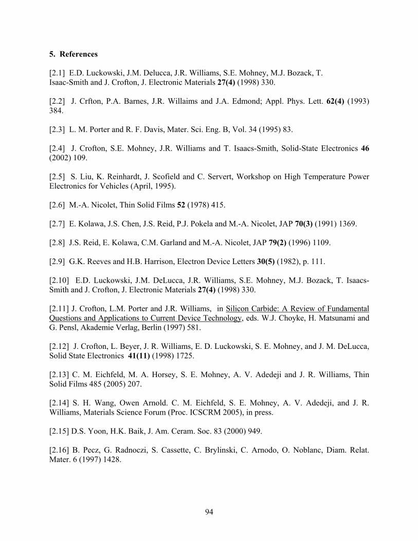
94
5. References [2.1] E.D. Luckowski, J.M. Delucca, J.R. Williams, S.E. Mohney, M.J. Bozack, T. Isaac-Smith and J. Crofton, J. Electronic Materials 27(4) (1998) 330. [2.2] J. Crfton, P.A. Barnes, J.R. Willaims and J.A. Edmond; Appl. Phys. Lett. 62(4) (1993) 384. [2.3] L. M. Porter and R. F. Davis, Mater. Sci. Eng. B, Vol. 34 (1995) 83. [2.4] J. Crofton, S.E. Mohney, J.R. Williams and T. Isaacs-Smith, Solid-State Electronics 46 (2002) 109. [2.5] S. Liu, K. Reinhardt, J. Scofield and C. Servert, Workshop on High Temperature Power Electronics for Vehicles (April, 1995). [2.6] M.-A. Nicolet, Thin Solid Films 52 (1978) 415. [2.7] E. Kolawa, J.S. Chen, J.S. Reid, P.J. Pokela and M.-A. Nicolet, JAP 70(3) (1991) 1369. [2.8] J.S. Reid, E. Kolawa, C.M. Garland and M.-A. Nicolet, JAP 79(2) (1996) 1109. [2.9] G.K. Reeves and H.B. Harrison, Electron Device Letters 30(5) (1982), p. 111. [2.10] E.D. Luckowski, J.M. DeLucca, J.R. Williams, S.E. Mohney, M.J. Bozack, T. Isaacs-Smith and J. Crofton, J. Electronic Materials 27(4) (1998) 330. [2.11] J. Crofton, L.M. Porter and J.R. Williams, in Silicon Carbide: A Review of Fundamental Questions and Applications to Current Device Technology, eds. W.J. Choyke, H. Matsunami and G. Pensl, Akademie Verlag, Berlin (1997) 581. [2.12] J. Crofton, L. Beyer, J. R. Williams, E. D. Luckowski, S. E. Mohney, and J. M. DeLucca, Solid State Electronics 41(11) (1998) 1725. [2.13] C. M. Eichfeld, M. A. Horsey, S. E. Mohney, A. V. Adedeji and J. R. Williams, Thin Solid Films 485 (2005) 207. [2.14] S. H. Wang, Owen Arnold. C. M. Eichfeld, S. E. Mohney, A. V. Adedeji, and J. R. Williams, Materials Science Forum (Proc. ICSCRM 2005), in press. [2.15] D.S. Yoon, H.K. Baik, J. Am. Ceram. Soc. 83 (2000) 949. [2.16] B. Pecz, G. Radnoczi, S. Cassette, C. Brylinski, C. Arnodo, O. Noblanc, Diam. Relat. Mater. 6 (1997) 1428.
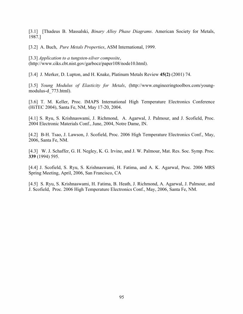
95
[3.1] [Thadeus B. Massalski, Binary Alloy Phase Diagrams. American Society for Metals, 1987.]
[3.2] A. Buch, Pure Metals Properties, ASM International, 1999. [3.3] Application to a tungsten-silver composite, (http://www.ciks.cbt.nist.gov/garbocz/paper108/node10.html). [3.4] J. Merker, D. Lupton, and H. Knake, Platinum Metals Review 45(2) (2001) 74. [3.5] Young Modulus of Elasticity for Metals, (http://www.engineeringtoolbox.com/young-modulus-d_773.html). [3.6] T. M. Keller, Proc. IMAPS International High Temperature Electronics Conference (HiTEC 2004), Santa Fe, NM, May 17-20, 2004. [4.1] S. Ryu, S. Krishnaswami, J. Richmond, A. Agarwal, J. Palmour, and J. Scofield, Proc. 2004 Electronic Materials Conf., June, 2004, Notre Dame, IN. [4.2] B-H. Tsao, J. Lawson, J. Scofield, Proc. 2006 High Temperature Electronics Conf., May, 2006, Santa Fe, NM. [4.3] W. J. Schaffer, G. H. Negley, K. G. Irvine, and J. W. Palmour, Mat. Res. Soc. Symp. Proc. 339 (1994) 595. [4.4] J. Scofield, S. Ryu, S. Krishnaswami, H. Fatima, and A. K. Agarwal, Proc. 2006 MRS Spring Meeting, April, 2006, San Francisco, CA [4.5] S. Ryu, S. Krishnaswami, H. Fatima, B. Heath, J. Richmond, A. Agarwal, J. Palmour, and J. Scofield, Proc. 2006 High Temperature Electronics Conf., May, 2006, Santa Fe, NM.

96
6. Appendix: Students Graduated and Publications/Presentations Students Graduated 1. C. Eichfield, Materials Science, MS, May, 2004 2. A. V. Adedeji, Physics, PhD, August, 2005 3. Cai Wang, Electrical & Computer Engineering, PhD, August, 2006 4. Yi Lui, Electrical & Computer Engineering, PhD, May, 2006
Publications (* denotes conference proceedings publication and conference presentation) *1. J. Crofton, J.R. Williams, A.V. Adedeji and J.D. Scofield, Ohmic Contacts to p-Type Epitaxial and Implanted 4H-SiC, Matls. Sci. Forum (Proc. of the 2005 International Conference on Silicon Carbide and Related Materials), in press. *2. S.H. Wang, C. M. Eichfield, M.A. Horsey B. Liu, S. E. Mohney, V. Adedeji and J.R. Williams, Tantalum-Rithenium Diffusion Barriers for Contacts to SiC, Matls. Sci. Forum (Proc. of the 2005 International Conference on Silicon Carbide and Related Materials), in press. *3. A. V. Adedeji C. Ahyi, J.R. Williams, S. Mohney , B. Liu and J.D. Schofield, Composite Ohmic Contacts to SiC for High Temperature Applications, Matls. Sci. Forum (Proc. of the 2005 International Conference on Silicon Carbide and Related Materials), in press. *4. S. E. Mohney, S. H. Wang, C. M. Eichfeld, M. A. Horsey, A. V. Adedeji, J. Williams, Composite Ohmic Contacts to SiC for High Temperature Applications, Matls. Sci. Forum (Proc. of the 2005 International Conference on Silicon Carbide and Related Materials), in press. 5. C.M. Eichfeld, M.A. Horsey, S.E. Mohney, A.V. Adedeji and J.R. Williams, Ta-Ru-N Diffusion Barriers for High Temperature Contacts to p-Type SiC, Thin Solid Films 485 (2005) 207. *6. R. Wayne Johnson and John Williams, Power Device Packaging Technologies for Extreme Environments, Proceedings of the IEEE Aerospace Conference, Big Sky Montana, March, 2005. *7. C. M. Eichfeld, M. A. Horsey, S. E. Mohney, A. V. Adedeji and J. R. Williams, “Ta-Ru-N Diffusion Barriers for High Temperature Metallizations to SiC,” TMS Electronic Materials Conference, Notre Dame, IN, June, 2004. *8. A. V. Adedeji, A. C. Ahyi, J. R. Williams, M. Horsey, S. E. Mohney and J. D. Scofield, Diffusion / Oxidation Barriers for Composite Metal Contacts to SiC, Proc. of the 2004 High Temperature Electronics Conf., Albuquerque, NM, May, 2004. *9. R. Wayne Johnson and John Williams, SiC Power Device Packaging Technologies for 300 to 350 oC Applications, Proc. of the 5th European Conference on Silicon Carbide and Related Materials, Bologna, Italy, August, 2004. INVITED PAPER.

97
*10. S. Ryu, S. Krishnaswami, J. Richmond, A. Agarwal, J. Palmour, and J. Scofield, 2.5 kV, 17 mΩ-cm2 4H-SiC JFETs, Proc. of the Electronic Materials Conf., June, 2004, Notre Dame, IN. *11. J. Scofield, S. Ryu, S. Krishnaswami, H. Fatima, and A. K. Agarwal, 1.8 kV, 10 mΩ-cm2 4H-SiC JFETs, Proc. of the MRS Spring Meeting, April, 2006, San Francisco, CA. *12. S. Ryu, S. Krishnaswami, H. Fatima, B. Heath, J. Richmond, A. Agarwal, J. Palmour, and J. Scofield, A Comparison of High Temperature Performance of SiC MOSFETs and JFETs, Proc. High Temperature Electronics Conf. May, 2006, Santa Fe, NM.