
AFL270XXS - Infineon TechnologiesLINE REJECTION MIL-STD-461, CS101, 30Hz to 50KHz Note 1 60 70 dB...
16
12/18/06 www.irf.com 1 AFL270XXS SERIES The AFL Series of DC/DC converters feature high power density with no derating over the full military temperature range. This series is offered as part of a complete family of converters providing single and dual output voltages and operating from nominal +28V or +270V inputs with output power ranging from 80W to 120W. For applications requiring higher output power, multiple converters can be operated in parallel. The internal current sharing circuits assure equal current distribution among the paralleled converters. This series incorporates International Rectifier’s proprietary magnetic pulse feedback technology providing optimum dynamic line and load regulation response. This feedback system samples the output voltage at the pulse width modulator fixed clock frequency, nominally 550KHz. Multiple converters can be synchronized to a system clock in the 500 KHz to 700KHz range or to the synchronization output of one converter. Undervoltage lockout, primary and secondary referenced inhibit, softstart and load fault protection are provided on all models. Description n 160V To 400V Input Range n 5V, 6V, 9V, 12V, 15V and 28V Outputs Available n High Power Density - up to 84W/in 3 n Up To 120W Output Power n Parallel Operation with Stress and Current Sharing n Low Profile (0.380") Seam Welded Package n Ceramic Feedthru Copper Core Pins n High Efficiency - to 87% n Full Military Temperature Range n Continuous Short Circuit and Overload Protection n Remote Sensing Terminals n Primary and Secondary Referenced Inhibit Functions n Line Rejection > 60dB - DC to 50KHz n External Synchronization Port n Fault Tolerant Design n Dual Output Versions Available n Standard Microcircuit Drawings Available Features AFL 270V Input, Single Output HYBRID-HIGH RELIABILITY DC/DC CONVERTER Manufactured in a facility fully qualified to MIL-PRF- 38534, these converters are fabricated utilizing DSCC qualified processes. For available screening options, refer to device screening table in the data sheet. Variations in electrical, mechanical and screening can be accommodated. Contact IR Santa Clara for special requirements. These converters are hermetically packaged in two enclosure variations, utilizing copper core pins to minimize resistive DC losses. Three lead styles are available, each fabricated with International Rectifier’s rugged ceramic lead-to-package seal assuring long term hermeticity in the most harsh environments. PD - 94435B
Transcript of AFL270XXS - Infineon TechnologiesLINE REJECTION MIL-STD-461, CS101, 30Hz to 50KHz Note 1 60 70 dB...

www.irf.com 1
AFL270XXS SERIES
The AFL Series of DC/DC converters feature high powerdensity with no derating over the full militarytemperature range. This series is offered as part of acomplete family of converters providing single and dualoutput voltages and operating from nominal +28V or+270V inputs with output power ranging from 80W to120W. For applications requiring higher output power,multiple converters can be operated in parallel. Theinternal current sharing circuits assure equal currentdistribution among the paralleled converters. This seriesincorporates International Rectifier’s proprietarymagnetic pulse feedback technology providingoptimum dynamic line and load regulation response.This feedback system samples the output voltage atthe pulse width modulator fixed clock frequency,nominally 550KHz. Multiple converters can besynchronized to a system clock in the 500 KHz to 700KHzrange or to the synchronization output of one converter.Undervoltage lockout, primary and secondaryreferenced inhibit, softstart and load fault protectionare provided on all models.
Description
160V To 400V Input Range 5V, 6V, 9V, 12V, 15V and 28V Outputs Available High Power Density - up to 84W/in3
Up To 120W Output Power Parallel Operation with Stress and Current Sharing Low Profile (0.380") Seam Welded Package Ceramic Feedthru Copper Core Pins High Efficiency - to 87% Full Military Temperature Range Continuous Short Circuit and Overload Protection Remote Sensing Terminals Primary and Secondary Referenced Inhibit Functions Line Rejection > 60dB - DC to 50KHz External Synchronization Port Fault Tolerant Design Dual Output Versions Available Standard Microcircuit Drawings Available
Features
AFL
270V Input, Single Output
HYBRID-HIGH RELIABILITYDC/DC CONVERTER
Manufactured in a facility fully qualified to MIL-PRF-38534, these converters are fabricated utilizing DSCCqualified processes. For available screening options,refer to device screening table in the data sheet.Variations in electrical, mechanical and screening canbe accommodated. Contact IR Santa Clara for specialrequirements.
These converters are hermetically packaged in twoenclosure variations, utilizing copper core pins tominimize resistive DC losses. Three lead styles areavailable, each fabricated with International Rectifier’srugged ceramic lead-to-package seal assuring longterm hermeticity in the most harsh environments.
PD - 94435B
2 www.irf.com
AFL270XXS Series
For Notes to Specifications, refer to page 4
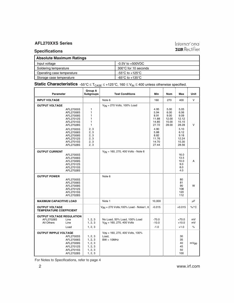
Static Characteristics -55°C ≤ TCASE ≤ +125°C, 160 ≤ VIN ≤ 400 unless otherwise specified.
Specifications
Input voltage -0.5V to +500VDC Soldering temperature 300°C for 10 seconds Operating case temperature -55°C to +125°C Storage case temperature -65°C to +135°C
Absolute Maximum Ratings
Parameter
Group A Subgroups
Test Conditions
Min
Nom
Max
Unit
INPUT VOLTAGE Note 6 160 270 400 V
OUTPUT VOLTAGE AFL27005S AFL27006S AFL27009S AFL27012S AFL27015S AFL27028S
AFL27005S AFL27006S AFL27009S AFL27012S AFL27015S AFL27028S
1 1 1 1 1 1
2, 3 2, 3 2, 3 2, 3 2, 3 2, 3
VIN = 270 Volts, 100% Load
4.95 5.94 8.91 11.88 14.85 27.72
4.90 5.88 8.82 11.76 14.70 27.44
5.00 6.00 9.00
12.00 15.00 28.00
5.05 6.06 9.09
12.12 15.15 28.28
5.10 6.12 9.18
12.24 15.30 28.56
V
OUTPUT CURRENT AFL27005S AFL27006S AFL27009S AFL27012S AFL27015S AFL27028S
VIN = 160, 270, 400 Volts - Note 6 16.0 13.5 10.0 9.0 8.0 4.0
A
OUTPUT POWER AFL27005S AFL27006S AFL27009S AFL27012S AFL27015S AFL27028S
Note 6 80 81 90 108 120 112
W
MAXIMUM CAPACITIVE LOAD Note 1 10,000 µF
OUTPUT VOLTAGE TEMPERATURE COEFFICIENT
VIN = 270 Volts,100% Load - Notes1, 6 -0.015 +0.015 %/°C
OUTPUT VOLTAGE REGULATION AFL27028S Line All Others Line
Load
1, 2, 3 1, 2, 3
1, 2, 3
No Load, 50% Load, 100% Load VIN = 160, 270, 400 Volts
-70.0 -10.0
-1.0
+70.0 +10.0
+1.0
mV mV
%
OUTPUT RIPPLE VOLTAGE AFL27005S AFL27006S AFL27009S AFL27012S AFL27015S AFL27028S
1, 2, 3 1, 2, 3 1, 2, 3 1, 2, 3 1, 2, 3 1, 2, 3
VIN = 160, 270, 400 Volts, 100% Load, BW = 10MHz
30 35 40 45 50 100
mVpp

www.irf.com 3
AFL270XXS Series
Static Characteristics (Continued)
For Notes to Specifications, refer to page 4
Parameter
Group A Subgroups
Test Conditions
Min
Nom
Max
Unit
INPUT CURRENT No Load Inhibit 1 Inhibit 2
1
2, 3 1, 2, 3 1, 2, 3
VIN = 270 Volts IOUT = 0 Pin 4 Shorted to Pin 2 Pin 12 Shorted to Pin 8
15.00 17.00 3.00 5.00
mA
INPUT RIPPLE CURRENT AFL27005S AFL27006S AFL27009S AFL27012S AFL27015S AFL27028S
1, 2, 3 1, 2, 3 1, 2, 3 1, 2, 3 1, 2, 3 1, 2, 3
VIN = 270 Volts, 100% Load
B.W. = 10MHz
60 60 70 70 80 80
mApp
CURRENT LIMIT POINT
Expressed as a Percentage of Full Rated Load
1 2 3
VOUT = 90% VNOM Note 5
115 105 125
125 115 140
%
LOAD FAULT POWER DISSIPATION Overload or Short Circuit
1, 2, 3
VIN = 270 Volts
30
W
EFFICIENCY AFL27005S AFL27006S AFL27009S AFL27012S AFL27015S AFL27028S
1, 2, 3 1, 2, 3 1, 2, 3 1, 2, 3 1, 2, 3 1, 2, 3
VIN = 270 Volts, 100% Load 78 79 80 82 83 82
82 83 84 85 87 85
%
ENABLE INPUTS (Inhibit Function) Converter Off Sink Current Converter On Sink Current
1, 2, 3
1, 2, 3
Logical Low, Pin 4 or Pin 12 Note 1 Logical High, Pin 4 and Pin 12 - Note 9Note 1
-0.5
2.0
0.8 100 50
100
V
µA V
µA
SWITCHING FREQUENCY 1, 2, 3 500 550 600 KHz
SYNCHRONIZATION INPUT Frequency Range Pulse Amplitude, Hi Pulse Amplitude, Lo Pulse Rise Time Pulse Duty Cycle
1, 2, 3 1, 2, 3 1, 2, 3
Note 1 Note 1
500 2.0 -0.5
20
700 10 0.8 100 80
KHz
V V ns %
ISOLATION 1 Input to Output or Any Pin to Case (except Pin 3). Test @ 500VDC
100 MΩ
DEVICE WEIGHT Slight Variations with Case Style 85 g
MTBF MIL-HDBK-217F, AIF @ TC = 70°C 300 KHrs
4 www.irf.com
AFL270XXS Series
Dynamic Characteristics -55°C ≤ TCASE ≤ +125°C, VIN = 270 Volts unless otherwise specified.
Parameter
Group A Subgroups
Test Conditions
Min
Nom
Max
Unit
LOAD TRANSIENT RESPONSE
AFL27005S Amplitude Recovery
Amplitude Recovery
AFL27006S Amplitude Recovery
Amplitude Recovery
AFL27009S Amplitude Recovery
Amplitude Recovery
AFL27012S Amplitude Recovery
Amplitude Recovery
AFL27015S Amplitude Recovery
Amplitude Recovery
AFL27028S Amplitude Recovery
Amplitude Recovery
4, 5, 6 4, 5, 6
4, 5, 6 4, 5, 6
4, 5, 6 4, 5, 6
4, 5, 6 4, 5, 6
4, 5, 6 4, 5, 6
4, 5, 6 4, 5, 6
4, 5, 6 4, 5, 6
4, 5, 6 4, 5, 6
4, 5, 6 4, 5, 6
4, 5, 6 4, 5, 6
4, 5, 6 4, 5, 6
4, 5, 6 4, 5, 6
Note 2, 8
Load Step 50% ⇔ 100%
Load Step 10% ⇔ 50%
Load Step 50% ⇔ 100%
Load Step 10% ⇔ 50%
Load Step 50% ⇔ 100%
Load Step 10% ⇔ 50%
Load Step 50% ⇔ 100%
Load Step 10% ⇔ 50%
Load Step 50% ⇔ 100%
Load Step 10% ⇔ 50%
Load Step 50% ⇔ 100%
Load Step 10% ⇔ 50%
-450
-450
-450
-450
-600
-600
-750
-750
-900
-900
-1200
-1200
450 200
450 400
450 200
450 400
600 200
600 400
750 200
750 400
900 200
900 400
1200 200
1200 400
mV µs
mV µs
mV µs
mV µs
mV µs
mV µs
mV µs
mV µs
mV µs
mV µs
mV µs
mV µs
LINE TRANSIENT RESPONSE
Amplitude Recovery
Note 1, 2, 3
VIN Step = 160 ⇔ 400 Volts
-500
500 500
mV µs
TURN-ON CHARACTERISTICS
Overshoot Delay
4, 5, 6 4, 5, 6
VIN = 160, 270, 400 Volts. Note 4
Enable 1, 2 on. (Pins 4, 12 high or open)
50
75
250 120
mV ms
LOAD FAULT RECOVERY Same as Turn On Characteristics.
LINE REJECTION MIL-STD-461, CS101, 30Hz to 50KHz Note 1
60 70 dB
Notes to Specifications:
1. Parameters not 100% tested but are guaranteed to the limits specified in the table.2. Recovery time is measured from the initiation of the transient to where VOUT has returned to within ±1.0%
of VOUT at 50% load.3. Line transient transition time ≥ 100µs.4. Turn-on delay is measured with an input voltage rise time of between 100V and 500V per millisecond.5. Current limit point is that condition of excess load causing output voltage to drop to 90% of nominal.6. Parameter verified as part of another test.7. All electrical tests are performed with the remote sense leads connected to the output leads at the load.8. Load transient transition time ≥ 10µs.9. Enable inputs internally pulled high. Nominal open circuit voltage ≈ 4.0VDC.

www.irf.com 5
AFL270XXS Series
Block DiagramFigure 1. AFL Single Output
Connection of the + and - sense leads at a remotely locatedload permits compensation for resistive voltage dropbetween the converter output and the load when they arephysically separated by a significant distance. Thisconnection allows regulation to the placard voltage at thepoint of application. When the remote sensing features is
Figure 2. Enable Input Equivalent Circuit
Pin 4 orPin 12
1N4148100K
290K
150K
2N3904
+5.6V
Disable
Pin 2 orPin 8
not used, the sense leads should be connected to theirrespective output terminals at the converter. Figure 3.illustrates a typical application.
Circuit Operation and Application Information
The AFL series of converters employ a forward switchedmode converter topology. (refer to Figure 1.) Operation ofthe device is initiated when a DC voltage whose magnitudeis within the specified input limits is applied between pins 1and 2. If pin 4 is enabled (at a logical 1 or open) the primarybias supply will begin generating a regulated housekeepingvoltage bringing the circuitry on the primary side of theconverter to life. Two power MOSFETs used to chop theDC input voltage into a high frequency square wave, applythis chopped voltage to the power transformer. As thisswitching is initiated, a voltage is impressed on a secondwinding of the power transformer which is then rectified andapplied to the primary bias supply. When this occurs, theinput voltage is shut out and the primary bias voltagebecomes exclusively internally generated.
Remote Sensing
Inhibiting Converter Output (Enable)As an alternative to application and removal of the DCvoltage to the input, the user can control the converteroutput by providing TTL compatible, positive logic signalsto either of two enable pins (pin 4 or 12). The distinctionbetween these two signal ports is that enable 1 (pin 4) isreferenced to the input return (pin 2) while enable 2 (pin 12)is referenced to the output return (pin 8). Thus, the userhas access to an inhibit function on either side of the isolationbarrier. Each port is internally pulled “high” so that whennot used, an open connection on both enable pins permitsnormal converter operation. When their use is desired, alogical “low” on either port will shut the converter down.
ERROR AMP
& REF
OUTPUT FILTER
INPUT FILTER
OUTPUT RETURN
+ INPUT
INPUT RETURN
CONTROL
1
2
4
3
5
6 SYNC INPUT
CURRENT SENSE
+ SENSE
RETURN SENSE
SENSE AMPLIFIER
ENABLE 2
SHARE SHARE
AMPLIFIER
7
11
10
9
12
8
+ OUTPUT
SYNC OUTPUT
ENABLE 1
CASE
PRIMARY BIAS SUPPLY
The switched voltage impressed on the secondary outputtransformer winding is rectified and filtered to provide theconverter output voltage. An error amplifier on the secondaryside compares the output voltage to a precision referenceand generates an error signal proportional to the difference.This error signal is magnetically coupled through thefeedback transformer into the controller section of theconverter varying the pulse width of the square wave signaldriving the MOSFETs, narrowing the width if the outputvoltage is too high and widening it if it is too low.
6 www.irf.com
AFL270XXS Series
high level of +2.0V. The sync output of another converterwhich has been designated as the master oscillator providesa convenient frequency source for this mode of operation.When external synchronization is not required, the sync inpin should be left unconnected thereby permitting theconverter to operate at its’ own internally set frequency.
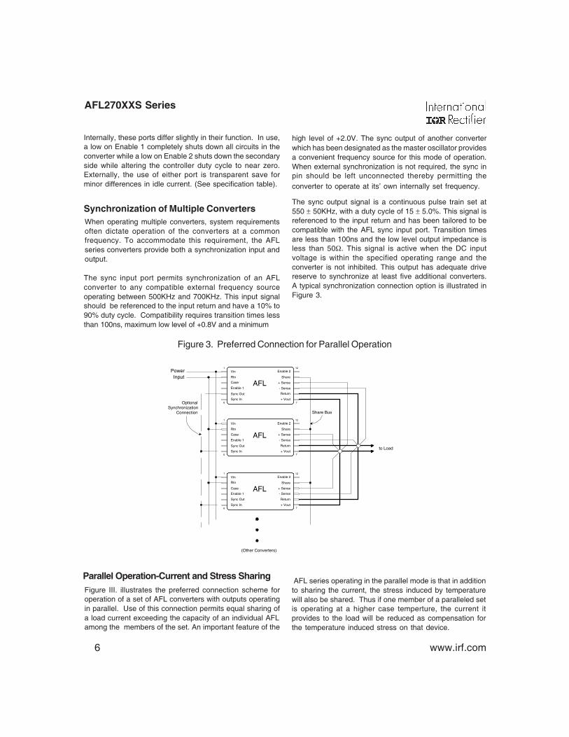
The sync output signal is a continuous pulse train set at550 ± 50KHz, with a duty cycle of 15 ± 5.0%. This signal isreferenced to the input return and has been tailored to becompatible with the AFL sync input port. Transition timesare less than 100ns and the low level output impedance isless than 50Ω. This signal is active when the DC inputvoltage is within the specified operating range and theconverter is not inhibited. This output has adequate drivereserve to synchronize at least five additional converters.A typical synchronization connection option is illustrated inFigure 3.
Figure 3. Preferred Connection for Parallel Operation
OptionalSynchronization
Connection
PowerInput
(Other Converters)
Share Bus
1
6
AFL
7
12
- Sense
Enable 2
+ Vout
Return
+ Sense
Share
Vin
Rtn
Case
Enable 1
Sync Out
Sync In
1
6
AFL
7
12
- Sense
Enable 2
+ Vout
Return
+ Sense
Share
Vin
Rtn
Case
Enable 1
Sync Out
Sync In
1
6
AFL
7
12
- Sense
Enable 2
+ Vout
Return
+ Sense
Share
Vin
Rtn
Case
Enable 1
Sync Out
Sync In
to Load
AFL series operating in the parallel mode is that inadditionto sharing the current, the stress induced by temperaturewill also be shared. Thus if one member of a paralleled setis operating at a higher case temperture, the current itprovides to the load will be reduced as compensation forthe temperature induced stress on that device.
When operating multiple converters, system requirementsoften dictate operation of the converters at a commonfrequency. To accommodate this requirement, the AFLseries converters provide both a synchronization input andoutput.
Figure III. illustrates the preferred connection scheme foroperation of a set of AFL converters with outputs operatingin parallel. Use of this connection permits equal sharing ofa load current exceeding the capacity of an individual AFLamong the members of the set. An important feature of the
Internally, these ports differ slightly in their function. In use,a low on Enable 1 completely shuts down all circuits in theconverter while a low on Enable 2 shuts down the secondaryside while altering the controller duty cycle to near zero.Externally, the use of either port is transparent save forminor differences in idle current. (See specification table).
Synchronization of Multiple Converters
Parallel Operation-Current and Stress Sharing
The sync input port permits synchronization of an AFLconverter to any compatible external frequency sourceoperating between 500KHz and 700KHz. This input signalshould be referenced to the input return and have a 10% to90% duty cycle. Compatibility requires transition times lessthan 100ns, maximum low level of +0.8V and a minimum
www.irf.com 7
AFL270XXS Series
for minor variations of either surface. While other availabletypes of heat conductive materials and compounds mayprovide similar performance, these alternatives are oftenless convinient and are frequently messy to use.
A conservative aid to estimating the total heat sink surfacearea (AHEAT SINK) required to set the maximum casetemperature rise (∆T) above ambient temperature is givenby the following expression:
A HEAT SINK ≈⎧⎨⎩
⎫⎬⎭
−−∆T
P803 00 85
143
.
.
.
where
∆T
P PEff
OUT
=
= = −⎧⎨⎩
⎫⎬⎭
Case temperature rise above ambient
Device dissipation in Watts1
1
∆T = 85 - 25 = 60°C
( )P = • −⎧⎨⎩
⎫⎬⎭
= • =120183
1 120 0 205 24 6.
. . W
and the required heat sink area is
A =60
80 24.6 inHEAT SINK 0.85•
⎧⎨⎩
⎫⎬⎭
− =−143
23 0 71.
.
From the Specification Table, the worst case full loadefficiency for this device is 83%; therefore the powerdissipation at full load is given by
Because of the incorporation of many innovativetechnological concepts, the AFL series of converters iscapable of providing very high output power from a packageof very small volume. These magnitudes of power densitycan only be obtained by combining high circuit efficiencywith effective methods of heat removal from the die junctions.This requirement has been effectively addressed inside thedevice; but when operating at maximum loads, a significantamount of heat will be generated and this heat must beconducted away from the case. To maintain the casetemperature at or below the specified maximum of 125°C,this heat must be transferred by conduction to anappropriate heat dissipater held in intimate contact with theconverter base-plate.
Because effectiveness of this heat transfer is dependenton the intimacy of the baseplate/heatsink interface, it isstrongly recommended that a high thermal conductivity heattransferance medium is inserted between the baseplateand heatsink. The material most frequently utilized at thefactory during all testing and burn-in processes is sold underthe trade name of Sil-Pad® 4001 . This particular productis an insulator but electrically conductive versions are alsoavailable. Use of these materials assures maximum surfacecontact with the heat dissipator thereby compensating
When operating in the shared mode, it is important thatsymmetry of connection be maintained as an assurance ofoptimum load sharing performance. Thus, converter outputsshould be connected to the load with equal lengths of wire ofthe same gauge and sense leads from each converter shouldbe connected to a common physical point, preferably at theload along with the converter output and return leads. Allconverters in a paralleled set must have their share pinsconnected together. This arrangement is diagrammaticallyillustrated in Figure III. showing the outputs and sense pinsconnected at a star point which is located close as possibleto the load.
As a consequence of the topology utilized in the currentsharing circuit, the share pin may be used for other functions.In applications requiring a single converter, the voltageappearing on the share pin may be used as a “currentmonitor”. The share pin open circuit voltage is nominally+1.00V at no load and increases linearly with increasingoutput current to +2.20V at full load. The share pin voltageis referenced to the output return pin.
Thus, a total heat sink surface area (including fins, if any) of71 in2 in this example, would limit case rise to 60°C aboveambient. A flat aluminum plate, 0.25" thick and of approximatedimension 4" by 9" (36 in2 per side) would suffice for thisapplication in a still air environment. Note that to meet thecriteria in this example, both sides of the plate requireunrestricted exposure to the ambient air.
1Sil-Pad is a registered Trade Mark of Bergquist, Minneapolis, MN
As an example, it is desired to maintain the case temperatureof an AFL27015S at ≤ +85°C in an area where the ambienttemperature is held at a constant +25°C; then
Thermal Considerations
8 www.irf.com
AFL270XXS Series
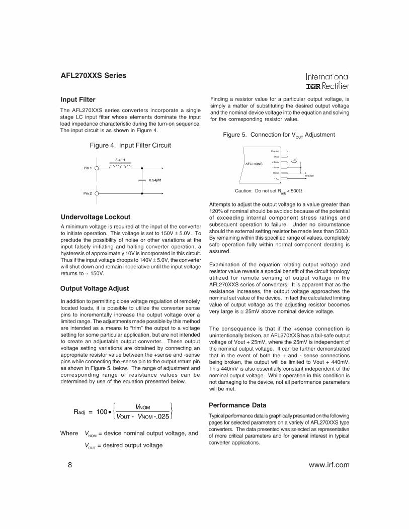
The AFL270XXS series converters incorporate a singlestage LC input filter whose elements dominate the inputload impedance characteristic during the turn-on sequence.The input circuit is as shown in Figure 4.
Figure 4. Input Filter Circuit
8.4µH
Pin 1
Pin 2
0.54µfd
A minimum voltage is required at the input of the converterto initiate operation. This voltage is set to 150V ± 5.0V. Topreclude the possibility of noise or other variations at theinput falsely initiating and halting converter operation, ahysteresis of approximately 10V is incorporated in this circuit.Thus if the input voltage droops to 140V ± 5.0V, the converterwill shut down and remain inoperative until the input voltagereturns to ≈ 150V.
In addition to permitting close voltage regulation of remotelylocated loads, it is possible to utilize the converter sensepins to incrementally increase the output voltage over alimited range. The adjustments made possible by this methodare intended as a means to “trim” the output to a voltagesetting for some particular application, but are not intendedto create an adjustable output converter. These outputvoltage setting variations are obtained by connecting anappropriate resistor value between the +sense and -sensepins while connecting the -sense pin to the output return pinas shown in Figure 5. below. The range of adjustment andcorresponding range of resistance values can bedetermined by use of the equation presented below.
R = 100- -.025
adjNOM
OUT NOM •
⎧⎨⎩
⎫⎬⎭
VV V
Where VNOM = device nominal output voltage, and
VOUT = desired output voltage
Finding a resistor value for a particular output voltage, issimply a matter of substituting the desired output voltageand the nominal device voltage into the equation and solvingfor the corresponding resistor value.
Figure 5. Connection for VOUT Adjustment
Enable 2
Share
+ Sense
- Sense
Return
+ Vout
To Load
RADJ
AFL270xxS
Caution: Do not set Radj
< 500Ω
Attempts to adjust the output voltage to a value greater than120% of nominal should be avoided because of the potentialof exceeding internal component stress ratings andsubsequent operation to failure. Under no circumstanceshould the external setting resistor be made less than 500Ω.By remaining within this specified range of values, completelysafe operation fully within normal component derating isassured.
Examination of the equation relating output voltage andresistor value reveals a special benefit of the circuit topologyutilized for remote sensing of output voltage in theAFL270XXS series of converters. It is apparent that as theresistance increases, the output voltage approaches thenominal set value of the device. In fact the calculated limitingvalue of output voltage as the adjusting resistor becomesvery large is ≅ 25mV above nominal device voltage.
The consequence is that if the +sense connection isunintentionally broken, an AFL270XXS has a fail-safe outputvoltage of Vout + 25mV, where the 25mV is independent ofthe nominal output voltage. It can be further demonstratedthat in the event of both the + and - sense connectionsbeing broken, the output will be limited to Vout + 440mV.This 440mV is also essentially constant independent of thenominal output voltage. While operation in this condition isnot damaging to the device, not all performance parameterswill be met.
Typical performance data is graphically presented on the followingpages for selected parameters on a variety of AFL270XXS typeconverters. The data presented was selected as representativeof more critical parameters and for general interest in typicalconverter applications.
Input Filter
Undervoltage Lockout
Output Voltage Adjust
Performance Data
www.irf.com 9
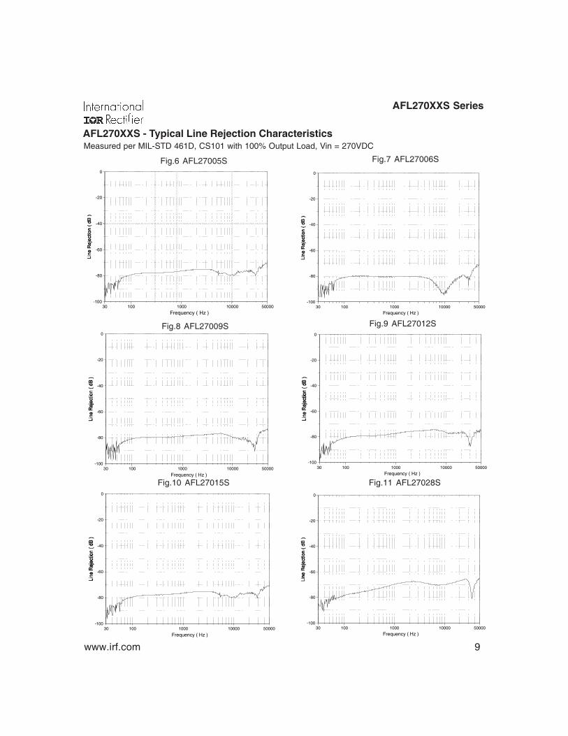
AFL270XXS Series
AFL270XXS - Typical Line Rejection CharacteristicsMeasured per MIL-STD 461D, CS101 with 100% Output Load, Vin = 270VDC
-100
-80
-60
-40
-20
0
30 100 1000 10000 50000
Frequency ( Hz ) -100
-80
-60
-40
-20
0
30 100 1000 10000 50000
Frequency ( Hz )
Fig.6 AFL27005S Fig.7 AFL27006S
-100
-80
-60
-40
-20
0
30 100 1000 10000 50000
Frequency ( Hz )
-100
-80
-60
-40
-20
0
30 100 1000 10000 50000
Frequency ( Hz )
Fig.8 AFL27009S Fig.9 AFL27012S
-100
-80
-60
-40
-20
0
30 100 1000 10000 50000
Frequency ( Hz )
Fig.10 AFL27015S Fig.11 AFL27028S
-100
-80
-60
-40
-20
0
30 100 1000 10000 50000
Frequency ( Hz )

10 www.irf.com
AFL270XXS Series
AFL270XXS Typical Efficiency CharacteristicsPresented for three values of Input Voltage.
Fig.12 AFL27005S Fig.13 AFL27006S
Fig.14 AFL27009S Fig.15 AFL27012S
Fig.16 AFL27015S Fig.17 AFL27028S
50
60
70
80
90
0 20 40 60 80 100Output Power ( Watts )
160V
270V
400V
55
65
75
85
95
0 20 40 60 80 100 120
Output Power ( Watts )
160V
270V
400V
50
60
70
80
90
0 20 40 60 80 100 120
Output Power ( Watts )
160V
270V
400V
50
60
70
80
90
0 20 40 60 80
Output Power ( Watts )
160V
270V
400V
50
60
70
80
90
0 20 40 60 80Output Power ( Watts )
160V
270V
400V
55
65
75
85
95
0 20 40 60 80 100 120
Output Power ( Watts )
160V
270V
400V

www.irf.com 11
AFL270XXS Series
Typical Performance Characteristics - AFL27005SOutput Load = 100%, Vin = 270VDC unless otherwise specified.
Fig.18 Turn-on Time, No Load
Fig.22 Output Load Transient Response50% Load to/from 100% Load
-1
0
1
2
3
4
5
6
70 75 80 85 90 95 100
Time from Application of Input Power ( msec )
-1
0
1
2
3
4
5
6
70 75 80 85 90 95 100
Time from Application of Input Power ( msec )
Fig.19 Turn-on Time, Full Load
-8
-4
0
4
8
0 2 4 6 8 10
Time ( usec )
-40
-20
0
20
40
0 2 4 6 8 10
Time ( usec )
Fig.20 Output Ripple Voltage Fig.21 Input Ripple Current
-400
-200
0
200
400
0 200 400 600 800 1000
Time ( usec )
-400
-200
0
200
400
0 200 400 600 800 1000
Time ( usec )
Fig.23 Output Load Transient Response10% Load to/from 50% Load
12 www.irf.com
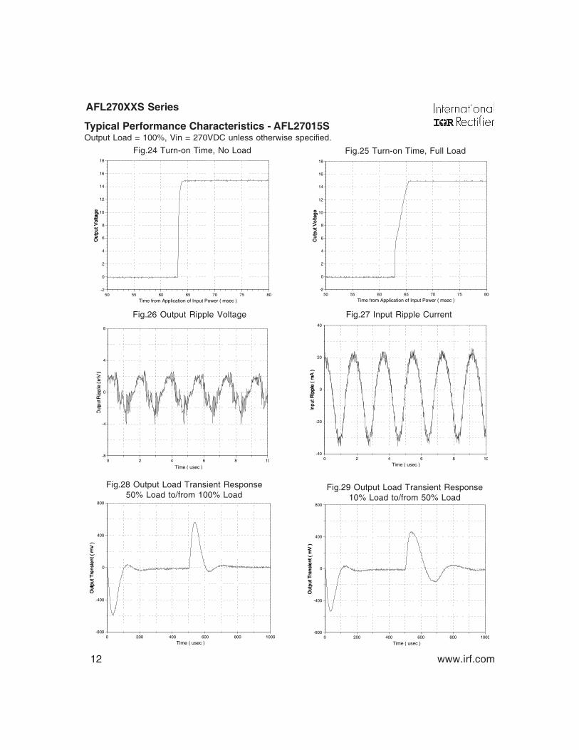
AFL270XXS Series
Typical Performance Characteristics - AFL27015SOutput Load = 100%, Vin = 270VDC unless otherwise specified.
Fig.24 Turn-on Time, No Load
Fig.28 Output Load Transient Response50% Load to/from 100% Load
Fig.25 Turn-on Time, Full Load
Fig.26 Output Ripple Voltage Fig.27 Input Ripple Current
Fig.29 Output Load Transient Response10% Load to/from 50% Load
-2
0
2
4
6
8
10
12
14
16
18
50 55 60 65 70 75 80
Time from Application of Input Power ( msec )
-2
0
2
4
6
8
10
12
14
16
18
50 55 60 65 70 75 80
Time from Application of Input Power ( msec )
-40
-20
0
20
40
0 2 4 6 8 10
Time ( usec )
-800
-400
0
400
800
0 200 400 600 800 1000
Time ( usec )
-800
-400
0
400
800
0 200 400 600 800 1000
Time ( usec )
-8
-4
0
4
8
0 2 4 6 8 10
Time ( usec )

www.irf.com 13
AFL270XXS Series
Typical Performance Characteristics - AFL27028SOutput Load = 100%, Vin = 270VDC unless otherwise specified.
Fig.30 Turn-on Time, No Load
Fig.34 Output Load Transient Response50% Load to/from 100% Load
Fig.31 Turn-on Time, Full Load
Fig.32 Output Ripple Voltage Fig.33 Input Ripple Current
Fig.35 Output Load Transient Response10% Load to/from 50% Load
-5
0
5
10
15
20
25
30
60 65 70 75 80 85 90
Time from Application of Input Power ( msec )
-5
0
5
10
15
20
25
30
60 65 70 75 80 85 90
Time from Application of Input Power ( msec )
-8
-4
0
4
8
0 2 4 6 8 10
Time ( usec )
-40
-20
0
20
40
0 2 4 6 8 10
Time ( usec )
-800
-400
0
400
800
0 200 400 600 800 1000
Time ( usec )
-800
-400
0
400
800
0 200 400 600 800 1000
Time ( usec )
14 www.irf.com
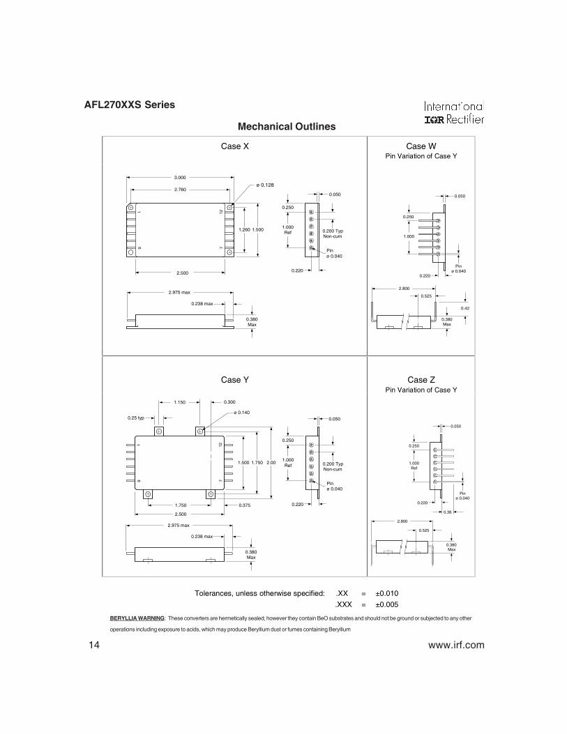
AFL270XXS Series
Mechanical Outlines
Case X
Case W Pin Variation of Case Y
1.260 1.500
2.500
2.760
3.000
ø 0.128
0.250
1.000Ref 0.200 Typ
Non-cum
0.050
0.220
Pinø 0.040
0.238 max
0.380Max
2.975 max
16 7
12
0.050
0.220
0.250
1.000
Pinø 0.040
0.525
0.380Max
2.800
0.42
Case Y Case Z Pin Variation of Case Y
1.500 1.750
2.500
0.25 typ
1.150
0.050
0.220
16 7
12
1.750 0.375
2.00
0.250
1.000Ref 0.200 Typ
Non-cum
Pinø 0.040
0.300
ø 0.140
0.238 max
0.380Max
2.975 max
0.050
0.220
0.250
1.000Ref
Pinø 0.040
0.525
0.380Max
2.800
0.36
BERYLLIA WARNING: These converters are hermetically sealed; however they contain BeO substrates and should not be ground or subjected to any other
operations including exposure to acids, which may produce Beryllium dust or fumes containing Beryllium
Tolerances, unless otherwise specified: .XX = ±0.010
.XXX = ±0.005
www.irf.com 15
AFL270XXS Series
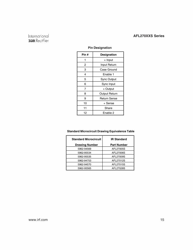
Pin Designation
Pin # Designation
1 + Input
2 Input Return
3 Case Ground
4 Enable 1
5 Sync Output
6 Sync Input
7 + Output
8 Output Return
9 Return Sense
10 + Sense
11 Share
12 Enable 2
Standard Microcircuit Drawing Equivalence Table
Standard Microcircuit IR Standard
Drawing Number Part Number5962-94569 AFL27005S
5962-95534 AFL27006S
5962-95535 AFL27009S
5962-94753 AFL27012S
5962-94570 AFL27015S
5962-95565 AFL27028S

16 www.irf.com
AFL270XXS Series
Part Numbering
Notes: Best commercial practice Sample tests at low and high temperatures -55°C to +105°C for AHE, ATO, ATW
WORLD HEADQUARTERS: 233 Kansas St., El Segundo, California 90245, Tel: (310) 322 3331IR SANTA CLARA: 2270 Martin Av., Santa Clara, California 95050, Tel: (408) 727-0500
Visit us at www.irf.com for sales contact information. Data and specifications subject to change without notice. 12/2006
Device Screening
Requirement MIL-STD-883 Method No Suffix ES HB CH
Temperature Range -20°C to +85°C -55°C to +125°C -55°C to +125°C -55°C to +125°C
Element Evaluation MIL-PRF-38534 N/A N/A N/A Class H
Non-Destructive
Bond Pull
Internal Visual 2017 Yes Yes Yes
Temperature Cycle 1010 N/A Cond B Cond C Cond C
Constant Acceleration 2001, Y1 Axis N/A 500 Gs 3000 Gs 3000 Gs
PIND 2020 N/A N/A N/A N/A
Burn-In 1015 N/A 48 hrs@hi temp 160 hrs@125°C 160 hrs@125°C
Final Electrical MIL-PRF-38534 25°C 25°C -55°C, +25°C, -55°C, +25°C,
( Group A ) & Specification +125°C +125°C
PDA MIL-PRF-38534 N/A N/A N/A 10%
Seal, Fine and Gross 1014 Cond A Cond A, C Cond A, C Cond A, C
Radiographic 2012 N/A N/A N/A N/A
External Visual 2009 Yes Yes Yes
N/A N/A2023 N/A N/A
AFL 270 05 S X /CH
Model
Input Voltage28 = 28V50 = 50V120 = 120V270 = 270V
Output Voltage05 = 5V, 06 = 6V 07 = 7V, 08 = 8V09 = 9V, 12 = 12V15 = 15V, 28 = 28V
OutputS = Single
Case Style W, X, Y, Z
Screening Level(Please refer to Screening Table) No suffix, ES, HB, CH