
AFBR-5710Z and AFBR-5715Z Families of Multi-Mode Small ... · 2 figure 1. sfp block diagram light...
20
AFBR-5710Z and AFBR-5715Z Families of Multi-Mode Small Form Factor Pluggable (SFP) Optical Transceivers with Optional DMI for Gigabit Ethernet (1.25 GBd) Data Sheet Features • ROHS-6 Compliant • Compliant to IEEE 802.3 Gigabit Ethernet (1.25GBd) 1000BaseSX • Optional Digital Diagnostic Monitoring available - AFBR-5710Z family: without DMI - AFBR-5715Z family: with DMI • Per SFF-8472, diagnostic features on AFBR-5715Z family enable Diagnostic Monitoring Interface for optical transceivers with real-time monitoring of: - Transmitted optical power - Received optical power - Laser bias current - Temperature - Supply voltage • Transceiver specifications according to SFP Multi- Source Agreement (SFF-8074i) and SFF-8472, Revision 9.3 • Manufactured in an ISO 9001 compliant facility • Hot-pluggable • Temperature options - (Extended) -10°C to +85°C - (Industrial) -40°C to +85°C • +3.3 V DC power supply • Industry leading EMI performance for high port den- sity • 850 nm Vertical Cavity Surface Emitting Laser (VCSEL) • Eye safety certified • LC-Duplex fiber connector compliant Applications • Ethernet Switch • Enterprise Router • Broadband aggregation and wireless infrastructure • Metro Ethernet multi-service access & provisioning platforms Description The AFBR-571xZ family of SFP optical transceivers offers the customer a wide range of design options, includ- ing optional DMI features (further described later), two temperature ranges (extended or industrial), and choice of standard or bail delatch. The AFBR-5715Z family targets those applications requiring DMI features. The AFBR-5710Z family is a streamlined product designed for those applications where DMI features are not needed. Throughout this document, AFBR-571xZ will be used to refer collectively to the product family encompassing this entire range of product options. Part Number Options The AFBR-571xZ SFP family includes the following prod- ucts: Part Number DMI Temperature Latch AFBR-5710LZ No Extended Standard AFBR-5710PZ No Extended Bail AFBR-5710ALZ No Industrial Standard AFBR-5710APZ No Industrial Bail AFBR-5715LZ Yes Extended Standard AFBR-5715PZ Yes Extended Bail AFBR-5715ALZ Yes Industrial Standard AFBR-5715APZ Yes Industrial Bail * Extended Temperature Range is -10 to 85 °C Industrial Temperature Range is -40 to 85 ° C Related Products • AFBR-5705Z family: Dual-Rate 1.25 GBd Ethernet (1000BASE-SX) & 1.0625 GBd Fiber Channel SFP with DMI • ABCU-5710RZ family : 1.25 GBd Ethernet (1000BASE-T) SFP for Cat5 cable • AFCT-5705Z family: 1.25 GBd Ethernet (1000BASE-LX) & 1.0265 GBd Fiber-Channel SFP with DMI Patent - www.avagotech.com/patents
Transcript of AFBR-5710Z and AFBR-5715Z Families of Multi-Mode Small ... · 2 figure 1. sfp block diagram light...

AFBR-5710Z and AFBR-5715ZFamilies of Multi-Mode Small Form Factor Pluggable (SFP) Optical Transceivers with Optional DMI for Gigabit Ethernet (1.25 GBd)
Data Sheet
Features• ROHS-6 Compliant• Compliant to IEEE 802.3 Gigabit Ethernet (1.25GBd)
1000BaseSX• Optional Digital Diagnostic Monitoring available
- AFBR-5710Z family: without DMI - AFBR-5715Z family: with DMI
• Per SFF-8472, diagnostic features on AFBR-5715Z family enable Diagnostic Monitoring Interface for optical transceivers with real-time monitoring of: - Transmitted optical power - Received optical power - Laser bias current - Temperature - Supply voltage
• Transceiver specifications according to SFP Multi-Source Agreement (SFF-8074i) and SFF-8472, Revision 9.3
• Manufactured in an ISO 9001 compliant facility• Hot-pluggable• Temperature options
- (Extended) -10°C to +85°C - (Industrial) -40°C to +85°C
• +3.3 V DC power supply• Industry leading EMI performance for high port den-
sity• 850 nm Vertical Cavity Surface Emitting Laser (VCSEL)• Eye safety certified• LC-Duplex fiber connector compliant
Applications • Ethernet Switch• Enterprise Router• Broadband aggregation and wireless infrastructure• Metro Ethernet multi-service access & provisioning
platforms
DescriptionThe AFBR-571xZ family of SFP optical transceivers offers the customer a wide range of design options, includ-ing optional DMI features (further described later), two temperature ranges (extended or industrial), and choice of standard or bail delatch. The AFBR-5715Z family targets those applications requiring DMI features. The AFBR-5710Z family is a streamlined product designed for those applications where DMI features are not needed. Throughout this document, AFBR-571xZ will be used to refer collectively to the product family encompassing this entire range of product options.
Part Number Options The AFBR-571xZ SFP family includes the following prod-ucts:
Part Number DMI Temperature Latch
AFBR-5710LZ No Extended Standard
AFBR-5710PZ No Extended Bail
AFBR-5710ALZ No Industrial Standard
AFBR-5710APZ No Industrial Bail
AFBR-5715LZ Yes Extended Standard
AFBR-5715PZ Yes Extended Bail
AFBR-5715ALZ Yes Industrial Standard
AFBR-5715APZ Yes Industrial Bail
* Extended Temperature Range is -10 to 85 °C Industrial Temperature Range is -40 to 85 ° C
Related Products• AFBR-5705Z family: Dual-Rate 1.25 GBd Ethernet
(1000BASE-SX) & 1.0625 GBd Fiber Channel SFP with DMI
• ABCU-5710RZ family : 1.25 GBd Ethernet (1000BASE-T) SFP for Cat5 cable
• AFCT-5705Z family: 1.25 GBd Ethernet (1000BASE-LX) & 1.0265 GBd Fiber-Channel SFP with DMI
Patent - www.avagotech.com/patents

2
Figure 1. SFP Block Diagram
LIGHT FROM FIBER
LIGHT TO FIBER
PHOTO-DETECTOR
RECEIVER
AMPLIFICATION& QUANTIZATION
RD+ (RECEIVE DATA)
RDÐ (RECEIVE DATA)
Rx LOSS OF SIGNAL
VCSEL
TRANSMITTER
LASERDRIVER &
SAFETYCIRCUITRY
TX_DISABLE
TD+ (TRANSMIT DATA)
TDÐ (TRANSMIT DATA)
TX_FAULT
ELECTRICAL INTERFACE
MOD-DEF2 (SDA)
MOD-DEF1 (SCL)
MOD-DEF0
CONTROLLER & MEMORY
OPTICAL INTERFACE
VEET20
TD–19
TD+18
VEET17
VCCT16
VCCR15
VEER14
RD+13
RD–12
VEER11
TOP OF BOARD
VEET1
TX FAULT2
TX DISABLE3
MOD-DEF(2)4
MOD-DEF(1)5
MOD-DEF(0)6
RATE SELECT7
LOS8
VEER9
VEER10
BOTTOM OF BOARD(AS VIEWED THROUGH TOP OF BOARD)
ENGAGEMENTSEQUENCE
3 2 1 3 2 1
Figure 2. Pin description of the SFP electrical interface.
OverviewThe AFBR-571xZ family of optical transceivers are com-pliant with the specifications set forth in the IEEE802.3 (1000BASE-SX) and the Small Form-Factor Pluggable (SFP) Multi-Source Agreement (MSA). This family of transceivers is qualified in accordance with Telcordia GR-468-CORE. Its primary application is servicing Gigabit Ethernet links between optical networking equipment.
The AFBR-571xZ offers maxi mum flexibility to designers, manufacturers, and operators of Gigabit Ethernet net-working equipment. A pluggable architec ture allows the module to be installed into MSA standard SFP ports at any time – even with the host equipment operating and online. This facilitates the rapid configuration of equip-ment to precisely the user’s needs – reducing inventory costs and network downtime. Compared with traditional transceivers, the size of the Small Form Factor package enables higher port densities.
Module DiagramsFigure 1 illustrates the major functional components of the AFBR-571xZ. The external configuration of the module is depicted in Figure 7. Figure 8 depicts the panel and host board footprints.

3
InstallationThe AFBR-571xZ can be installed in or removed from any MSA-compliant Pluggable Small Form Factor port regard-less of whether the host equipment is operating or not. The module is simply inserted, electrical-interface first, under finger-pressure. Controlled hot-plugging is ensured by 3-stage pin sequencing at the electrical interface. This printed circuit board card-edge connector is depicted in Figure 2.
As the module is inserted, first contact is made by the housing ground shield, discharging any potentially com-ponent-damaging static electricity. Ground pins engage next and are followed by Tx and Rx power supplies. Finally, signal lines are connected. Pin functions and sequencing are listed in Table 2.
Transmitter SectionThe transmitter section includes the Transmitter Optical Sub assembly (TOSA) and laser driver circuitry. The TOSA, containing an 850 nm VCSEL (Vertical Cavity Surface Emit-ting Laser) light source, is located at the optical interface and mates with the LC optical connector. The TOSA is driven by a custom IC, which converts differential logic signals into an analog laser diode drive current. This Tx driver circuit regu-lates the optical power at a constant level provided the data pattern is DC balanced (8B10B code for example).
Transmit Disable (Tx_Disable)The AFBR-571xZ accepts a TTL and CMOS compatible transmit disable control signal input (pin 3) which shuts down the transmitter optical output. A high signal imple-ments this function while a low signal allows normal transceiver operation. In the event of a fault (e.g. eye safety circuit activated), cycling this control signal resets the module as depicted in Figure 6. An internal pull-up resistor disables the transceiver transmitter until the host pulls the input low. Host systems should allow a 10ms interval between successive assertions of this control signal. Tx_Disable can also be asserted via the 2-wire serial interface (address A2h, byte 110, bit 6) and monitored (address A2h, byte 110, bit 7).
The contents of A2h, byte 110, bit 6 are logic OR’d with hardware Tx_Disable (pin 3) to control transmitter opera-tion.
Transmit Fault (Tx_Fault)A catastrophic laser fault will activate the transmitter signal, TX_FAULT, and disable the laser. This signal is an open collec-tor output (pull-up required on the host board). A low signal indicates normal laser operation and a high signal indicates a fault. The TX_FAULT will be latched high when a laser fault occurs and is cleared by toggling the TX_DISABLE input or power cycling the transceiver. The transmitter fault condition can also be monitored via the 2-wire serial interface (address A2, byte 110, bit 2).
Eye Safety CircuitThe AFBR-571xZ provides Class 1 eye safety by design and has been tested for compliance with the requirements listed in Table 1. The eye safety circuit continu ously moni-tors optical output power levels and will disable the trans-mitter and assert a TX_FAULT signal upon detecting an unsafe condition. Such unsafe conditions can be created by inputs from the host board (Vcc fluxuation, unbalanced code) or faults within the module.
Receiver SectionThe receiver section includes the Receiver Optical Subas-sembly (ROSA) and amplification/quantization circuitry. The ROSA, containing a PIN photodiode and custom trans-im-pedance preamplifier, is located at the optical interface and mates with the LC optical connector. The ROSA is mated to a custom IC that provides post-amplification and quantiza-tion. Also included is a Loss Of Signal (LOS) detection circuit.
Receiver Loss of Signal (Rx_LOS)The Loss Of Signal (LOS) output indicates an unusable optical input power level. The Loss Of Signal thresholds are set to indicate a definite optical fault has occurred (e.g., disconnected or broken fiber connection to receiver, failed transmitter, etc.).
The post-amplification IC includes transition detection circuitry which monitors the ac level of incoming optical signals and provides a TTL/CMOS compatible status signal to the host (pin 8). An adequate optical input results in a low Rx_LOS output while a high Rx_LOS output indicates an unusable optical input. The Rx_LOS thresholds are fac-tory-set so that a high output indicates a definite optical fault has occurred. For the AFBR-5715Z family, Rx_LOS can also be monitored via the 2-wire serial interface (address A2h, byte 110, bit 1).

4
Functional I/OThe AFBR-571xZ accepts industry standard differential signals such as LVPECL and CML within the scope of the SFP MSA. To simplify board requirements, transmitter bias resistors and ac coupling capacitors are incorporated, per SFF-8074i, and hence are not required on the host board. The module is AC-coupled and internally terminated.
Figure 3 illustrates a recommended interface circuit to link the AFBR-571xZ to the supporting Physical Layer integrated circuits.
Timing diagrams for the MSA compliant control signals implemented in this module are depicted in Figure 6.
The AFBR-571xZ interfaces with the host circuit board through twenty I/O pins (SFP electrical connector) identified by function in Table 2. The AFBR-571xZ high speed transmit and receive interfaces require SFP MSA compliant signal lines on the host board. The Tx_Disable, Tx_Fault, and Rx_LOS lines require TTL lines on the host board (per SFF-8074i) if used. If an application chooses not to take advantage of the functionality of these pins, care must be taken to ground Tx_Disable (for normal operation).
Figure 3. Typical application configuration.
LASER DRIVER& EYE SAFETY
CIRCUITRY
50 Ω
50 Ω
SO1+
SO1–
AMPLIFICATION&
QUANTIZATION
50 Ω
50 Ω
SI1+
SI1–
VREFR
TBCEWRAP
RBCRX_RATE
RX_LOS
GPIO(X)GPIO(X)
GP14
TX_FAULT
GP04
SYNCLOOP
SYN1RC1(0:1)
RFCT
TX[0:9]
RX[0:9]
TX_FAULT
TX_DISABLE
VEET
RD+
RD–
RX_LOS
MOD_DEF2EEPROMMOD_DEF1
MOD_DEF0
REF_RATE
NOTE: * 4.7 k Ω < RES < 10 kΩ
VCCT,R
125 MHz
AVAGOAFBR-571xZ
VCCT
1 µH
1 µH10 µF 0.1 µF
VCCT,R
VCCR10µF
0.1µF
0.1µF
AVAGOHDMP-1687
RRCM0
CC
REFCLK
MACASIC
*RES *RES *RES *RES
VEER
TD+
TD–
CC
R
*RES
HOUSINGGROUND
*RES
Digital Diagnostic Interface and Serial Identification (EEPROM)The entire AFBR-571xZ family complies with the SFF-8074i SFP specification. The AFBR-5715Z family further complies with SFF-8472, the SFP specification for Digital Diagnostic Monitoring Interface. Both specifications can be found at http://www.sffcommittee.org.
The AFBR-571xZ features an EEPROM for Serial ID, which contains the product data stored for retrieval by host equipment. This data is accessed via the 2-wire serial EEPROM protocol of the ATMEL AT24C01A or similar, in compliance with the industry standard SFP Multi-Source Agreement. The base EEPROM memory, bytes 0-255 at memory address 0xA0, is organized in compliance with SFF-8074i. Contents of this serial ID memory are shown in Table 10.
The I2C accessible memory page address 0xB0 is used internally by SFP for the test and diagnostic purposes and it is reserved.
5
As an enhancement to the conventional SFP interface defined in SFF-8074i, the AFBR-5715Z family is compliant to SFF-8472 (digital diagnostic interface for optical trans-ceivers). This new digital diagnostic information is stored in bytes 0-255 at memory address 0xA2.Using the 2-wire serial interface defined in the MSA, the AFBR-5715Z provides real time temperature, supply voltage, laser bias current, laser average output power and received input power. These parameters are internally calibrated, per the MSA.
The digital diagnostic interface also adds the ability to disable the transmitter (TX_DISABLE), monitor for Trans-mitter Faults (TX_FAULT), and monitor for Receiver Loss of Signal (RX_LOS).
The new diagnostic information provides the oppor-tunity for Predictive Failure Identification, Compliance Prediction, Fault Isolation and Component Monitoring.
Predictive Failure IdentificationThe predictive failure feature allows a host to identify potential link problems before system performance is impacted. Prior identification of link problems enables a host to service an application via “fail over” to a redun-dant link or replace a suspect device, maintaining system uptime in the process. For applications where ultra-high system uptime is required, a digital SFP provides a means to monitor two real-time laser metrics associated with ob-serving laser degradation and predicting failure: average laser bias current (Tx_Bias) and average laser optical power (Tx_Power).
Compliance PredictionCompliance prediction is the ability to determine if an optical transceiver is operating within its operating and environmental requirements. AFBR-5715Z devices provide real-time access to transceiver internal supply voltage and temperature, allowing a host to identify potential
component compliance issues. Received optical power is also available to assess compliance of a cable plant and remote transmitter. When operating out of requirements, the link cannot guarantee error free transmission.
Fault IsolationThe fault isolation feature allows a host to quickly pin-point the location of a link failure, minimizing downtime. For optical links, the ability to identify a fault at a local device, remote device or cable plant is crucial to speeding service of an installation. AFBR-5715Z real-time monitors of Tx_Bias, Tx_Power, Vcc, Temperature and Rx_Power can be used to assess local transceiver current operating conditions. In addition, status flags Tx_Disable and Rx Loss of Signal (LOS) are mirrored in memory and available via the two-wire serial interface.
Component MonitoringComponent evaluation is a more casual use of the AFBR-5715Z real-time monitors of Tx_Bias, Tx_Power, Vcc, Tem-perature and Rx_Power. Potential uses are as debugging aids for system installation and design, and transceiver parametric evaluation for factory or field qualification. For example, temperature per module can be observed in high density applications to facilitate thermal evaluation of blades, PCI cards and systems.
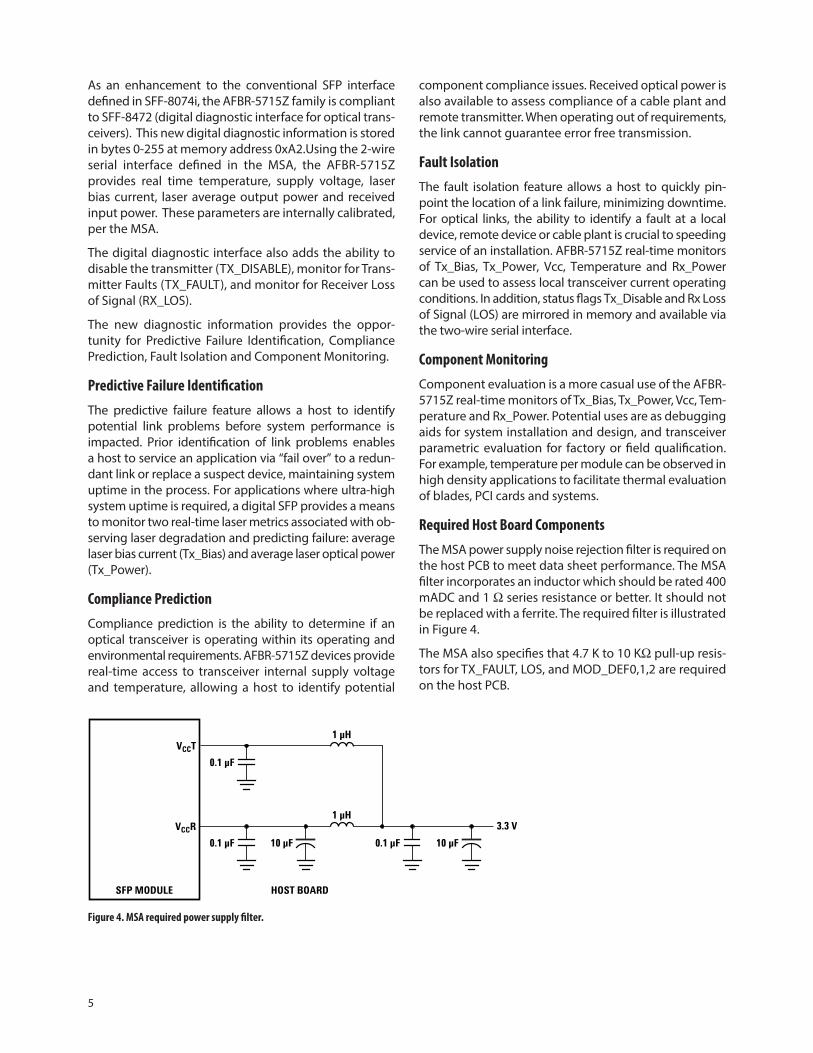
Required Host Board ComponentsThe MSA power supply noise rejection filter is required on the host PCB to meet data sheet performance. The MSA filter incorporates an inductor which should be rated 400 mADC and 1 Ω series resistance or better. It should not be replaced with a ferrite. The required filter is illustrated in Figure 4.
The MSA also specifies that 4.7 K to 10 KΩ pull-up resis-tors for TX_FAULT, LOS, and MOD_DEF0,1,2 are required on the host PCB.
1 µH
1 µH
0.1 µF
VCCR
SFP MODULE
10 µF
VCCT
0.1 µF 10 µF
3.3 V
HOST BOARD
0.1 µF
Figure 4. MSA required power supply filter.

6
Fiber CompatibilityThe AFBR-571xZ transciever is capable of transmission at 2 to 550 meters with 50/125 µm fiber, and at 2 to 275 meters with 62.5 125 µm fiber, for 1.25 GBd Ethernet. It is capable of transmission up to 500m with 50/125 µm fiber and up to 300m with 62.5/125 µm fiber, for 1.0625 GBd Fiber Channel.
Application SupportTo assist in the transceiver evaluation process, Agilent offers a 1.25 Gbd Gigabit Ethernet evaluation board which facilitates testing of the AFBR-571xZ. It can be obtained through the Agilent Field Organization by ref-erencing Agilent part number HFBR-0571.
A Reference Design including the AFBR-571xZ and the HDMP-1687 GigaBit Quad SerDes is available. It may be obtained through the Agilent Field Sales organization.
Regulatory ComplianceSee Table 1 for transceiver Regulatory Compliance. Certi-fication level is dependent on the overall configuration of the host equipment. The transceiver performance is offered as a figure of merit to assist the designer.
Electrostatic Discharge (ESD)The AFBR-571xZ exceeds typical industry standards and is compatible with ESD levels found in typical manufactur-ing and operating environments as described in Table 1.
There are two design cases in which immunity to ESD damage is important.
The first case is during handling of the transceiver prior to insertion into the transceiver port. To protect the trans-ceiver, it’s important to use normal ESD handling precau-tions. These precautions include using grounded wrist straps, work benches, and floor mats in ESD controlled areas. The ESD sensitivity of the AFBR-571xZ is compat-ible with typical industry production environments.
The second case to consider is static discharges to the exterior of the host equipment chassis after installation. To the extent that the optical interface is exposed to the outside of the host equipment chassis, it may be subject to system-level ESD requirements.
Electromagnetic Interference (EMI)Equipment using the AFBR-571xZ family of transceivers is typically required to meet the require ments of the FCC in the United States, CENELEC EN55022 (CISPR 22) in Europe, and VCCI in Japan.
The metal housing and shielded design of the AFBR-571xZ minimize the EMI challenge facing the host equip-ment designer.
EMI ImmunityEquipment hosting AFBR-571xZ modules will be sub-jected to radio-frequency electromagnetic fields in some environments. The transceiver has excellent immunity to such fields due to its shielded design.
FlammabilityThe AFBR-571xZ transceiver is made of metal and high strength, heat resistant, chemically resistant, and UL 94V-0 flame retardant plastic.
Customer Manufacturing ProcessesThis module is pluggable and is not designed for aqueous wash, IR reflow, or wave soldering processes.

7
Table 1. Regulatory Compliance
Feature Test Method PerformanceElectrostatic Discharge (ESD)to the Electrical Pins
JEDEC/EIAJESD22-A114-A Class 2 (> +2000 Volts)
Electrostatic Discharge (ESD) to the Duplex LC Reseptacle
Variation of IEC 6100-4-2 Typically withstands at least 25 kV without damage when the duplex LC connector receptacle is contacted by a Human Body Model probe
Electromagnetic Interference(EMI)
FCC Class B CENELEC EN55022 Class B (CISPR 22A) VCCI Class 1
Applications with high SFP port counts are expected to be compliant; however, margins are dependent on customer board and chassis design.
Immunity Variation of IEC 61000-4-3 Typically shows a negligible effect from a 10 V/m field swept from 80 to 1000 MHz applied to the transceiver without a chassis enclosure.
Eye Safety US FDA CDRH AEL Class 1 EN(IEC)60825-1,2, EN60950 Class 1
CDRH certification #9720151-57 TUV file RR72102090.01
Component Recognition Underwriters Laboratories and Canadian Standards Association Joint Component Recognition for Information Technology Equipment Including Electrical Business Equipment
UL File #E173874
ROHS Compliance Less than 1000ppm of: cadmium, lead, mercury, hexavalent chromium, polybrominated biphenyls, and polybrominated biphenyl ethers.
CautionThere are no user serviceable parts nor any maintenance required for the AFBR-571xZ. All adjustments are made at the factory before shipment to our customers. Tampering with, modifying, misusing or improp erly handling the AFBR-571xZ will void the product warranty. It may also result in improper operation of the AFBR-571xZ circuitry, and possible overstress of the laser source. Device deg-radation or product failure may result. Connection of the AFBR-571xZ to a non-Gigabit Ethernet compliant or non-Fiber Channel compliant optical source, operating above the recommended absolute maximum conditions or operating the AFBR-571xZ in a manner inconsistent with its design and function may result in hazardous radiation exposure and may be considered an act of modifying or manufacturing a laser product. The person(s) performing such an act is required by law to re-certify and re-identify the laser product under the provisions of U.S. 21 CFR (Subchapter J).

8
Table 2. Pin Description
Pin Name Function/DescriptionEngagement Order (insertion) Notes
1 VeeT Transmitter Ground 1
2 TX Fault Transmitter Fault Indication 3 1
3 TX Disable Transmitter Disable - Module disables on high or open 3 2
4 MOD-DEF2 Module Definition 2 - Two wire serial ID interface 3 3
5 MOD-DEF1 Module Definition 1 - Two wire serial ID interface 3 3
6 MOD-DEF0 Module Definition 0 - Grounded in module 3 3
7 Rate Selection Not Connected 3
8 LOS Loss of Signal 3 4
9 VeeR Receiver Ground 1
10 VeeR Receiver Ground 1
11 VeeR Receiver Ground 1
12 RD- Inverse Received Data Out 3 5
13 RD+ Received Data Out 3 5
14 VeeR Reciver Ground 1
15 VccR Receiver Power -3.3 V ±5% 2 6
16 VccT Transmitter Power -3.3 V ±5% 2 6
17 VeeT Transmitter Ground 1
18 TD+ Transmitter Data In 3 7
19 TD- Inverse Transmitter Data In 3 7
20 VeeT Transmitter Ground 1
Notes:1. TX Fault is an open collector/drain output which should be pulled up externally with a 4.7KΩ – 10 KΩ resistor on the host board to a supply
<VccT+0.3 V or VccR+0.3 V. When high, this output indicates a laser fault of some kind. Low indicates normal operation. In the low state, the output will be pulled to < 0.8 V.
2. TX disable input is used to shut down the laser output per the state table below. It is pulled up within the module with a 4.7-10 KΩ resistor. Low (0 – 0.8 V): Transmitter on Between (0.8 V and 2.0 V): Undefined High (2.0 – 3.465 V): Transmitter Disabled Open: Transmitter Disabled
3. Mod-Def 0,1,2. These are the module definition pins. They should be pulled up with a 4.7-10 KΩ resistor on the host board to a supply less than VccT +0.3 V or VccR+0.3 V. Mod-Def 0 is grounded by the module to indicate that the module is present Mod-Def 1 is clock line of two wire serial interface for optional serial ID Mod-Def 2 is data line of two wire serial interface for optional serial ID
4. LOS (Loss of Signal) is an open collector/drain output which should be pulled up externally with a 4.7 K – 10 KΩ resistor on the host board to a supply < VccT,R+0.3 V. When high, this output indicates the received optical power is below the worst case receiver sensitivity (as defined by the standard in use). Low indicates normal operatio0n. In the low state, the output will be pulled to < 0.8 V.
5. RD-/+: These are the differential receiver outputs. They are AC coupled 100 Ω differential lines which should be terminated with 100 Ω differential at the user SERDES. The AC coupling is done inside the module and is thus not required on the host board. The voltage swing on these lines must be between 370 and 2000 mV differential (185 – 1000 mV single ended) according to the MSA. Typically it will be 1500mv differential.
6. VccR and VccT are the receiver and transmitter power supplies. They are defined as 3.135 – 3.465 V at the SFP connector pin. The in-rush current will typically be no more than 30 mA above steady state supply current after 500 nanoseconds.
7. TD-/+: These are the differential transmitter inputs. They are AC coupled differential lines with 100 Ω differential termination inside the module. The AC coupling is done inside the module and is thus not required on the host board. The inputs will accept differential swings of 500 – 2400 mV (250 – 1200 mV single ended). However, the applicable recommended differential voltage swing is found in Table 5.

9
Table 3. Absolute Maximum Ratings
Parameter Symbol Minimum Maximum Unit NotesAmbient Storage Temperature(Non-operating)
Ts -40 +100 °C 1, 2
Case Temperature TC -40 +85 °C 1, 2
Relative Humidity RH 5 95 % 1
Supply Voltage VCCT,R -0.5 3.8 V 1, 2, 3
Low Speed Input Voltage VIN -0.5 VCC+0.5 V 1
Notes:1. Absolute Maximum Ratings are those values beyond which damage to the device may occur if these limits are exceeded. See Reliability Data
Sheet for specific reliability performance.2. Between Absolute Maximum Ratings and the Recommended Operating Conditions functional performance is not intended, device reliability
is not implied, and damage to the device may occur.3. The module supply voltages, VCCT and VCCR, must not differ by more than 0.5V or damage to the device may occur.
Table 4. Recommended Operating Conditions
Parameter Symbol Minimum Typical Maximum Unit NotesCase Temperature AFBR-571xLZ/PZ AFBR-571xALZ/APZ
TCTC
-10-40
2525
8585
°C°C
1, 21, 2
Supply Voltage VCC 3.135 3.3 3.465 V 1
Notes:1. Recommended Operating Conditions are those within which functional performance within data sheet characteristics is intended.2. Refer to the Reliability Data Sheet for specific reliability performance predictions.
Table 5. Transceiver Electrical Characteristics
Parameter Symbol Minimum Typical Maximum Unit NotesModule Supply Current ICC 160 220 mA
Power Dissipation PDISS 530 765 mW
Power Supply Noise Rejection(peak-peak)
PSNR 100 mVPP 1
Data input:Transmitter Differential Input Voltage (TD +/-)
VI 500 2400 mVPP 2
Data Output:Receiver Differential Output Voltage (RD +/-)
VO 370 1500 2000 mVPP 3
Receive Data Rise & Fall Times Trf 220 ps
Low Speed Outputs:Transmit Fault (TX_FAULT) Loss of Signal (LOS), MOD_DEF2
VOH 2.0 VCCT,R+0.3 V 4
VOL 0 0.8 V
Low Speed Inputs:Transmitter Disable(TX_DISABLE), MOD_DEF 1, MOD_DEF 2
VIH 2.0 VCC V 5
VIL 0 0.8 V
Notes:1. Measured at the input of the required MSA Filter on host board.2. Internally AC coupled and terminated to 100 Ω differential load.3. Internally AC coupled, but requires a 100 Ω differential termination at or internal to Serializer/Deserializer.4. Pulled up externally with a 4.7-10 KΩ resistor on the host board to VCCT,R.5. Mod_Def1 and Mod_Def2 must be pulled up externally with a 4.7-10 KΩ resistor on the host board to VCCT,R.

10
Table 7. Receiver Optical Characteristics
Parameter Symbol Minimum Typical Maximum Unit NotesOptical Input Power PR -17 0 dBm
Receiver Sensitivity (Optical Input Power)
PRMIN -21 -17 dBm
Stressed Receiver Sensitivity -12.5 dBm 62.5/125 mm fiber
-13.5 dBm 50/125 mm fiber
Total Jitter(TP3 to TP4 Contribution 1.25GBd)
TJ 266 ps
0.332 UI
Return Loss -12 dB
LOS De-Asserted PD - -17 dBm
LOS Asserted PA -30 dBm
LOS Hysterisis PD-PA 3 dB
Table 6. Transmitter Optical Characteristics
Parameter Symbol Minimum Typical Maximum Unit NotesOutput Optical Power (Average) POUT -9.5 -6.5 -3 dBm 1
Optical Extinction Ratio ER 9 12 dB
Center Wavelength lC 830 850 860 nm
Spectral Width - rms s 0.85 nm
Optical Rise/Fall Time Trise/fall 150 260 ps
Relative Intensity Noise RIN -117 dB/Hz
Total Jitter (TP1 to TP2 Contribution TJ 227 ps
0.284 UI
Pout TX_DISABLE Assorted POFF -35 dBm
Notes:1. 50/125 µm fiber with NA = 0.2, 62.5/125 µm fiber with NA = 0.275.
Figure 5a. Gigabit Ethernet transmitter eye mask diagram Figure 5b. Typical AFBR-571xZ eye mask diagram
80
50
20
0 22 37.5 78
NORMALIZED TIME (% OF UNIT INTERVAL)
NORM
ALIZ
ED A
MPL
ITUD
E (%
)
100
100
0
130
62.5
–20
0.80
0.50
0.20
1.00
0
1.30
–0.20
NORM
ALIZ
ED A
MPL
ITUD
E0 0.22 0.375 0.78 1.00.625
NORMALIZED TIME (UNIT INTERVAL)

11
Table 10. Transceiver SOFT DIAGNOSTIC Timing Characteristics
Parameter Symbol Minimum Maximum Unit NotesHardware TX_DISABLE Assert Time t_off 10 µs Note 1
Hardware TX_DISABLE Negate Time t_on 1 ms Note 2
Time to initialize, including reset of TX_FAULT t_init 300 ms Note 3
Hardware TX_FAULT Assert Time t_fault 100 µs Note 4
Hardware TX_DISABLE to Reset t_reset 10 µs Note 5
Hardware RX_LOS Assert Time t_loss_on 100 µs Note 6
Hardware RX_LOS De-Assert Time t_loss_off 100 µs Note 7
Software TX_DISABLE Assert Time t_off_soft 100 ms Note 8
Software TX_DISABLE Negate Time t_on_soft 100 ms Note 9
Software Tx_FAULT Assert Time t_fault_soft 100 ms Note 10
Software Rx_LOS Assert Time t_loss_on_soft 100 ms Note 11
Software Rx_LOS Deassert Time t_loss_off_soft 100 ms Note 12
Analog parameter data ready t_data 1000 ms Note 13
Serial bus hardware ready t_serial 300 ms Note 14
Write Cycle Time t_write 10 ms Note 15
Serial ID Clock Rate f_serial_clock 400 kHz
Notes:1. Time from rising edge of TX_DISABLE to when the optical output falls below 10% of nominal.2. Time from falling edge of TX_DISABLE to when the modulated optical output rises above 90% of nominal.3. Time from power on or falling edge of Tx_Disable to when the modulated optical output rises above 90% of nominal.4. From power on or negation of TX_FAULT using TX_DISABLE.5. Time TX_DISABLE must be held high to reset the laser fault shutdown circuitry.6. Time from loss of optical signal to Rx_LOS Assertion.7. Time from valid optical signal to Rx_LOS De-Assertion.8. Time from two-wire interface assertion of TX_DISABLE (A2h, byte 110, bit 6) to when the optical output falls below 10% of nominal. Measured
from falling clock edge after stop bit of write transaction.9. Time from two-wire interface de-assertion of TX_DISABLE (A2h, byte 110, bit 6) to when the modulated optical output rises above 90% of
nominal.10. Time from fault to two-wire interface TX_FAULT (A2h, byte 110, bit 2) asserted.11. Time for two-wire interface assertion of Rx_LOS (A2h, byte 110, bit 1) from loss of optical signal.12. Time for two-wire interface de-assertion of Rx_LOS (A2h, byte 110, bit 1) from presence of valid optical signal.13. From power on to data ready bit asserted (A2h, byte 110, bit 0). Data ready indicates analog monitoring circuitry is functional.14. Time from power on until module is ready for data transmission over the serial bus (reads or writes over A0h and A2h).15. Time from stop bit to completion of a 1-8 byte write command.

12
Figure 6. Transceiver timing diagrams (Module installed except where noted).
TX_FAULT
V CC > 3.15 V
t_init
TX_DISABLE
TRANSMITTED SIGNAL
t_init
TX_FAULT
V CC > 3.15 V
TX_DISABLE
TRANSMITTED SIGNAL
t-init: TX DISABLE NEGATED t-init: TX DISABLE ASSERTED
TX_FAULT
V CC > 3.15 V
t_init
TX_DISABLE
TRANSMITTED SIGNALt_off
TX_FAULT
TX_DISABLE
TRANSMITTED SIGNAL
t-init: TX DISABLE NEGATED, MODULE HOT PLUGGED t-off & t-on: TX DISABLE ASSERTED THEN NEGATED
INSERTION
t_on
TX_FAULT
OCCURANCE OF FAULT
t_fault
TX_DISABLE
TRANSMITTED SIGNAL
TX_FAULT
OCCURANCE OF FAULT
TX_DISABLE
TRANSMITTED SIGNAL
t-fault: TX FAULT ASSERTED, TX SIGNAL NOT RECOVERED t-reset: TX DISABLE ASSERTED THEN NEGATED, TX SIGNAL RECOVERED
t_resett_init** SFP SHALL CLEAR TX_FAULT IN
t_init IF THE FAILURE IS TRANSIENT
TX_FAULT
OCCURANCE OF FAULT
t_fault2
TX_DISABLE
TRANSMITTED SIGNAL
OCCURANCE OF LOSS
LOS
t-fault2: TX DISABLE ASSERTED THEN NEGATED, TX SIGNAL NOT RECOVERED
NOTE: t_fault2 timing is typically 1.7 to 2 ms.
t-loss-on & t-loss-off
t_loss_ont_init*
t_reset* SFP SHALL CLEAR T_FAULT IN t_init IF THE FAILURE IS TRANSIENT
t_loss_off
OPTICAL SIGNAL
Table 9. Transceiver Digital Diagnostic Monitor (Real Time Sense) Characteristics
Parameter Symbol Min. Units NotesTransceiver Internal TemperatureAccuracy
TINT ±3.0 °C Temperature is measured internal to the transceiver.Valid from = -40°C to 85°C case temperature.
Transceiver Internal SupplyVoltage Accuracy
VINT ±0.1 V Supply voltage is measured internal to the transceiverand can, with less accuracy, be correlated to voltage at the SFP Vcc pin. Valid over 3.3 V ± 5%.
Transmitter Laser DC Bias CurrentAccuracy
IINT ±10 % IINT is better than ±10% of the nominal value.
Transmitted Average OpticalOutput Power Accuracy
PT ±3.0 dB Coupled into 50/125 µm multi-mode fiber. Valid from 100 µW to 500 µW, avg.
Received Average Optical InputPower Accuracy
PR ±3.0 dB Coupled from 50/125 µm multi-mode fiber. Valid from 31 µW to 500 µW, avg.

13
Table 10. EEPROM Serial ID Memory Contents, Page A0h
ByteDecimal
#Hex
DataNotes
ByteDecimal
#Hex
DataNotes
0 03 SFP physical device 37 00 Vendor OUI (Note 4)1 04 SFP function defined by serial ID only 38 17 Vendor OUI (Note 4)2 07 LC optical connector 39 6A Vendor OUI (Note 4)3 00 40 41 "A" - Vendor Part Number ASCII character4 00 41 46 "F" - Vendor Part Number ASCII character5 00 42 42 "B" - Vendor Part Number ASCII character6 01 1000BaseSX 43 52 "R" - Vendor Part Number ASCII character7 00 44 2D "-" - Vendor Part Number ASCII character8 00 45 35 "5" - Vendor Part Number ASCII character9 00 46 37 "7" - Vendor Part Number ASCII character10 00 47 31 "1" - Vendor Part Number ASCII character11 01 Compatible with 8B/10B encoded data 48 Note 512 0C 1200Mbps nominal bit rate (1.25Gbps) 49 Note 513 00 50 Note 514 00 51 Note 515 00 52 20 “ “ - Vendor Part Number ASCII character16 37 550m of 50/125mm fiber @ 1.25Gbps
(Note 2)53 20 " " - Vendor Part Number ASCII character
17 1B 275m of 62.5/125mm fiber @ 1.25Gbps (Note 3)
54 20 " " - Vendor Part Number ASCII character
18 00 55 20 " " - Vendor Part Number ASCII character19 00 56 20 " " - Vendor Revision Number ASCII character20 41 'A' - Vendor Name ASCII character 57 20 " " - Vendor Revision Number ASCII character21 56 "V" - Vendor Name ASCII character 58 20 “ “ - Vendor Revision Number ASCII character22 41 "A" - Vendor Name ASCII character 59 20 “ “ - Vendor Revision Number ASCII character23 47 "G"- - Vendor Name ASCII character 60 03 Hex Byte of Laser Wavelength (Note 6)24 4F "O" - Vendor Name ASCII character 61 52 Hex Byte of Laser Wavelength (Note 6)25 20 " " - Vendor Name ASCII character 62 0026 20 “ “ - Vendor Name ASCII character 63 Checksum for bytes 0-62 (Note 7)27 20 “ “ - Vendor Name ASCII character 64 0028 20 “ “ - Vendor Name ASCII character 65 1A Hardware SFP TX_DISABLE, TX_FAULT, & RX_LOS29 20 “ “ - Vendor Name ASCIIcharacter 66 0030 20 “ “ - Vendor Name ASCIIcharacter 67 0031 20 “ “ - Vendor Name ASCIIcharacter 68-83 Vendor Serial Number, ASCII (Note 8)32 20 “ “ - Vendor Name ASCIIcharacter 84-91 Vendor Date Code, ASCII (Note 9)33 20 “ “ - Vendor Name ASCIIcharacter 92 Note 534 20 “ “ - Vendor Name ASCIIcharacter 93 Note 535 20 “ “ - Vendor Name ASCIIcharacter 94 Note 536 00 95 Checksum for bytes 64-94 (Note 7)
96 - 255 00Notes:1. FC-PI speed 100 MBytes/sec is a serial bit rate of 1.0625 GBit/sec.2. Link distance with 50/125µm cable at 1.25Gbps is 550m.3. Link distance with 62.5/125µm cable at 1.25Gbps is 275m.4. The IEEE Organizationally Unique Identifier (OUI) assigned to Avago Technologies is 00-17-6A (3 bytes of hex).5. See Table 11 for part number extensions and data-fields.6. Laser wavelength is represented in 16 unsigned bits. The hex representation of 850nm is 0352.7. Addresses 63 and 95 are checksums calculated per SFF-8472 and SFF-8074, and stored prior to product shipment.8. Addresses 68-83 specify the module’s ASCII serial number and will vary by unit.9. Addresses 84-91 specify the module’s ASCII date code and will vary according to manufactured date-code.

14
Table 11. Part Number Extensions
AFBR-5710ALZ AFBR-5710APZ AFBR-5710LZ AFBR-5710PZAddress Hex ASCII Address Hex ASCII Address Hex ASCII Address Hex ASCII
48 30 0 48 30 0 48 30 0 48 30 0
49 41 A 49 41 A 49 4C L 49 50 P
50 4C L 50 50 P 50 5A Z 50 5A Z
51 5A Z 51 5A Z 51 20 51 20
92 00 92 00 92 00 92 00
93 00 93 00 93 00 93 00
94 00 94 00 94 00 94 00
AFBR-5715ALZ AFBR-5715APZ AFBR-5715LZ AFBR-5715PZ
Address Hex ASCII Address Hex ASCII Address Hex ASCII Address Hex ASCII
48 35 5 48 35 5 48 35 5 48 35 5
49 41 A 49 41 A 49 4C L 49 50 P
50 4C L 50 50 P 50 5A Z 50 5A Z
51 5A Z 51 5A Z 51 20 51 20
92 68 92 68 92 68 92 68
93 F0 93 F0 93 F0 93 F0
94 01 94 01 94 01 94 01

15
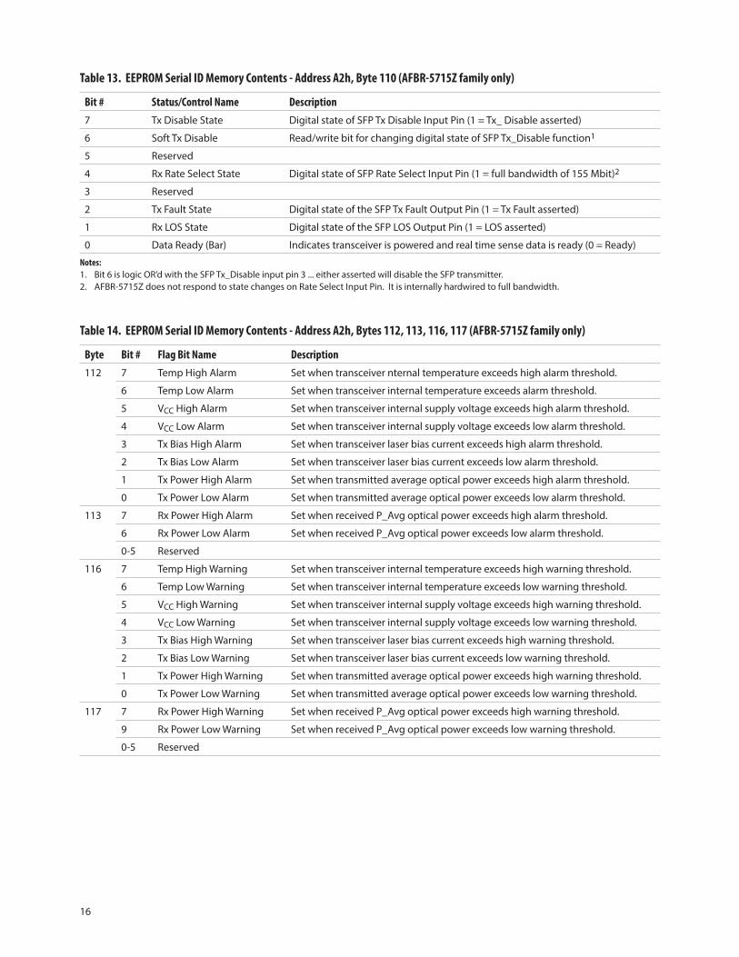
Table 12. EEPROM Serial ID Memory Contents - Address A2h (AFBR-5715Z family only)
Byte #Decimal Notes
Byte #Decimal Notes
Byte #Decimal Notes
0 Temp H Alarm MSB1 26 Tx Pwr L Alarm MSB4 104 Real Time Rx PAV MSB5
1 Temp H Alarm LSB1 27 Tx Pwr L Alarm LSB4 105 Real Time Rx PAV LSB5
2 Temp L Alarm MSB1 28 Tx Pwr H Warning MSB4 106 Reserved
3 Temp L Alarm LSB1 29 Tx Pwr H Warning LSB4 107 Reserved
4 Temp H Warning MSB1 30 Tx Pwr L Warning MSB4 108 Reserved
5 Temp H Warning LSB1 31 Tx Pwr L Warning LSB4 109 Reserved
6 Temp L Warning MSB1 32 Rx Pwr H Alarm MSB5 110 Status/Control - see Table 13
7 Temp L Warning LSB1 33 Rx Pwr H Alarm LSB5 111 Reserved
8 VCC H Alarm MSB2 34 Rx Pwr L Alarm MSB5 112 Flag Bits - see Table 14
9 VCC H Alarm LSB2 35 Rx Pwr L Alarm LSB5 113 Flag Bit - see Table 14
10 VCC L Alarm MSB2 36 Rx Pwr H Warning MSB5 114 Reserved
11 VCC L Alarm LSB2 37 Rx Pwr H Warning LSB5 115 Reserved
12 VCC H Warning MSB2 38 Rx Pwr L Warning MSB5 116 Flag Bits - see Table 14
13 VCC H Warning LSB2 39 Rx Pwr L Warning LSB5 117 Flag Bits - see Table 14
14 VCC L Warning MSB2 40-55 Reserved 118 Reserved
15 VCC L Warning LSB2 56-94 External Calibration Constants6 119 Reserved
16 Tx Bias H Alarm MSB3 95 Checksum for Bytes 0-947 120-122 Reserved
17 Tx Bias H Alarm LSB3 96 Real Time Temperature MSB1 123
18 Tx Bias L Alarm MSB3 97 Real Time Temperature LSB1 124
19 Tx Bias L Alarm LSB3 98 Real Time Vcc MSB2 125
20 Tx Bias H Warning MSB3 99 Real Time Vcc LSB2 126
21 Tx Bias H Warning LSB3 100 Real Time Tx Bias MSB3 127 Reserved8
22 Tx Bias L Warning MSB3 101 Real Time Tx Bias LSB3 128-247 Customer Writable9
23 Tx Bias L Warning LSB3 102 Real Time Tx Power MSB4 248-255 Vendor Specific
24 Tx Pwr H Alarm MSB4 103 Real Time Tx Power LSB4
25 Tx Pwr H Alarm LSB4
Notes:1. Temperature (Temp) is decoded as a 16 bit signed twos compliment integer in increments of 1/256 °C.2. Supply voltage (VCC) is decoded as a 16 bit unsigned integer in increments of 100 µV.3. Laser bias current (Tx Bias) is decoded as a 16 bit unsigned integer in increments of 2 µA.4. Transmitted average optical power (Tx Pwr) is decoded as a 16 bit unsigned integer in increments of 0.1 µW.5. Received average optical power (Rx Pwr) is decoded as a 16 bit unsigned integer in increments of 0.1 µW.6. Bytes 55-94 are not intended from use with AFBR-5715Z, but have been set to default values per SFF-8472.7. Bytes 95 is a checksum calculated (per SFF-8472) and stored prior to product shipment.8. Byte 127 accepts a write but performs no action (reserved legacy byte).9. Bytes 128-247 are write enabled (customer writable).
16
Table 13. EEPROM Serial ID Memory Contents - Address A2h, Byte 110 (AFBR-5715Z family only)
Bit # Status/Control Name Description7 Tx Disable State Digital state of SFP Tx Disable Input Pin (1 = Tx_ Disable asserted)
6 Soft Tx Disable Read/write bit for changing digital state of SFP Tx_Disable function1
5 Reserved
4 Rx Rate Select State Digital state of SFP Rate Select Input Pin (1 = full bandwidth of 155 Mbit)2
3 Reserved
2 Tx Fault State Digital state of the SFP Tx Fault Output Pin (1 = Tx Fault asserted)
1 Rx LOS State Digital state of the SFP LOS Output Pin (1 = LOS asserted)
0 Data Ready (Bar) Indicates transceiver is powered and real time sense data is ready (0 = Ready)
Notes:1. Bit 6 is logic OR’d with the SFP Tx_Disable input pin 3 ... either asserted will disable the SFP transmitter.2. AFBR-5715Z does not respond to state changes on Rate Select Input Pin. It is internally hardwired to full bandwidth.
Table 14. EEPROM Serial ID Memory Contents - Address A2h, Bytes 112, 113, 116, 117 (AFBR-5715Z family only)
Byte Bit # Flag Bit Name Description112 7 Temp High Alarm Set when transceiver nternal temperature exceeds high alarm threshold.
6 Temp Low Alarm Set when transceiver internal temperature exceeds alarm threshold.
5 VCC High Alarm Set when transceiver internal supply voltage exceeds high alarm threshold.
4 VCC Low Alarm Set when transceiver internal supply voltage exceeds low alarm threshold.
3 Tx Bias High Alarm Set when transceiver laser bias current exceeds high alarm threshold.
2 Tx Bias Low Alarm Set when transceiver laser bias current exceeds low alarm threshold.
1 Tx Power High Alarm Set when transmitted average optical power exceeds high alarm threshold.
0 Tx Power Low Alarm Set when transmitted average optical power exceeds low alarm threshold.
113 7 Rx Power High Alarm Set when received P_Avg optical power exceeds high alarm threshold.
6 Rx Power Low Alarm Set when received P_Avg optical power exceeds low alarm threshold.
0-5 Reserved
116 7 Temp High Warning Set when transceiver internal temperature exceeds high warning threshold.
6 Temp Low Warning Set when transceiver internal temperature exceeds low warning threshold.
5 VCC High Warning Set when transceiver internal supply voltage exceeds high warning threshold.
4 VCC Low Warning Set when transceiver internal supply voltage exceeds low warning threshold.
3 Tx Bias High Warning Set when transceiver laser bias current exceeds high warning threshold.
2 Tx Bias Low Warning Set when transceiver laser bias current exceeds low warning threshold.
1 Tx Power High Warning Set when transmitted average optical power exceeds high warning threshold.
0 Tx Power Low Warning Set when transmitted average optical power exceeds low warning threshold.
117 7 Rx Power High Warning Set when received P_Avg optical power exceeds high warning threshold.
9 Rx Power Low Warning Set when received P_Avg optical power exceeds low warning threshold.
0-5 Reserved
17
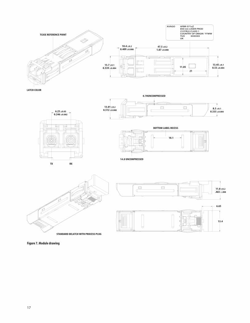
Figure 7. Module drawing
14.8 UNCOMPRESSED
TX RX
STANDARD DELATCH WITH PROCESS PLUG
6.65
13.4
11.8 ±0.2.465 ±.008
LATCH COLOR
0.70UNCOMPRESSED
BOTTOM LABEL RECESS
18.1
8.5 ±0.10.335 ±0.004
13.01 ±0.20.512 ±0.0086.25 ±0.05
0.246 ±0.002
13.7 ±0.10.539 ±0.004
13.45 ±0.10.53 ±0.004
10.4 ±0.20.409 ±0.008
47.5 ±0.21.87 ±0.008
TCASE REFERENCE POINT
2111.05
AVAGO AFBR-571xZ850 nm LASER PROD21CFR(J) CLASS 1COUNTRY OF ORIGIN YYWWTUV XXXXXXUK

18
Figure 8. SFP host board mechanical layout
2x 1.7
20x 0.5 ± 0.030.9
2 ± 0.05 TYP.0.06 L A S B S
10.53 11.93
20
1011
PIN 1
20
10 11
PIN 1
0.8TYP.
10.939.6
2x 1.55 ± 0.05
3.25
4
32
11
26.8 511x 2.0
3x 10
41.3
42.3
10x 1.05 ± 0.01
16.25REF. 14.25
11.088.58
5.68
11x 2.0
11.939.6
4.8
8.48
A
3.68
SEE DETAIL 19x 0.95 ± 0.05
2.5
7.17.2
2.5
34.5
16.25MIN. PITCH
Y X
DETAIL 1
∅ 0.85 ± 0.05
PCBEDGE
0.06 S A S B S
∅ 0.1 L A S B S
∅ 0.1 L X A S
∅0.1 S X A S∅ 0.1 S X Y
3x 10
B
NOTES1. PADS AND VIAS ARE CHASSIS GROUND2. THROUGH HOLES, PLATING OPTIONAL.3. HATCHED AREA DENOTES COMPONENT AND TRACE KEEPOUT (EXCEPT CHASSIS GROUND).4. AREA DENOTES COMPONENT KEEPOUT (TRACES ALLOWED).
DIMENSIONS IN MILLIMETERS

19
Figure 9. Assembly drawing
15(0.59)
41.73 ± 0.5(1.64 ± 0.02)
3.5 ± 0.3(0.14 ± 0.01)
1.7 ± 0.9(0.07 ± 0.04)
BEZEL
PCB
AREAFOR
PROCESSPLUG
10(0.39)
TO PCB
REF
0.4 ± 0.1(0.02 ± 0.004)BELOW PCB
10.4 ± 0.1(0.41 ± 0.004)
15.25 ± 0.1(0.60 ± 0.004)
MSA-SPECIFIED BEZEL
16.25 ± 0.1(0.64 ± 0.004)
MIN. PITCH
DIMENSIONS ARE IN MILLIMETERS (INCHES).
11(0.43)
1.5(0.06)
BELOW PCB
REF.
9.8(0.39)
CAGE ASSEMBLY
REF.
MAX.
MAX.

For product information and a complete list of distributors, please go to our web site: www.avagotech.com
Avago, Avago Technologies, and the A logo are trademarks of Avago Technologies in the United States and other countries.Data subject to change. Copyright © 2005-2016 Avago Technologies. All rights reserved. Obsoletes AV01-0181ENAV02-3012EN - January 7, 2016
Ordering InformationPlease contact your local field sales engineer or one of Avago Technologies franchised distributors for ordering infor-mation. For technical information, please visit Avago Technologies’ web-page at www.avagotech.com or contact one of Avago Technologies’ regional Technical Response Centers. For information related to SFF Committee documentation visit www.sffcommittee.org.