AEC to MILSPEC Comparison - NASA
28
NEPP Workshop at NASA Goddard June 15, 2020 Sultan Ali Lilani - Integra Technologies Allyson Yarborough – Aerospace Corp Larry Harzstark – Aerospace Corp Mike Cozzolino – Aerospace Corp AEC to MILSPEC Comparison
Transcript of AEC to MILSPEC Comparison - NASA

NEPP Workshop at NASA GoddardJune 15, 2020
Sultan Ali Lilani - Integra TechnologiesAllyson Yarborough – Aerospace Corp
Larry Harzstark – Aerospace CorpMike Cozzolino – Aerospace Corp
AEC to MILSPEC Comparison

1-800-622-2382www.Integra-tech.com
Agenda
AEC vs Mil Grade / Space Grade Overview –Allyson Yarborough
Microcircuits - AEC vs Mil Grade / Space Grade – Larry Harzstark
Discretes - AEC vs Mil Grade / Space Grade –Sultan Lilani
Passive - AEC vs Mil Grade / Space Grade –Mike Cozzolino

1-800-622-2382www.Integra-tech.com
AEC vs Mil Grade / Space Grade Overview Allyson Yarborough

1-800-622-2382www.Integra-tech.com
AEC vs Mil Grade / Space Grade Overview Item COTs AEC Mil / Space Grade Parts
Application Suitability Non-critical Small Sats / Less Than 5 Year Missions / Low Orbit
All Applications / Durations (Depending Upon Level)
Typical Screening (lot by lot)
25C Electrical 3 Temp Electrical Temp CycleX-Ray3 Temp ElectricalBurn-InLead / PIND (Hermetic Package)
Qual One Time / Major Changes One Time / Major Changes Every Lot
Reliability Stress Testing Non-sequential; Each Individual Failure Mode Assessed Separately
Non-sequential; Each Individual Failure Mode Assessed Separately
Periodic Reliability Monitor Tests on Product and Technology
Radiation Tolerance No No Yes for Space
DPA Required No No Yes for Space

1-800-622-2382www.Integra-tech.com
AEC vs Mil Grade / Space Grade OverviewItem COTs AEC Mil / Space Grade Parts
Typical Package Type Plastic / Non-Hermetic Plastic / Non-Hermetic HermeticPlastic / Non-Hermetic (Limited)
Manufacturing Location Control
No Yes Yes (Lot by Lot and by Wafer for Radiation)
Lot Date Code Control No No Yes - Homogeneous
PCN Control No Yes Yes
SPC Depends on Manufacturer Extensive - PPAP Controlled Extensive
Tin Whisker Mitigation Lead Finish: Pure Tin Lead Finish: Pure Tin Lead Finish: Tin/Lead and Gold
Availability Wide Wide Limited - Older Technologies Fade Out After Time. New Technology Devices Behind COTs/AEC
Lead Time Off The Shelf Some Times Off The Shelf Typically Long Lead Times Compared to COTs/AEC
EOL Longer Longer Longest
Cost Inexpensive Not so Expensive Expensive

1-800-622-2382www.Integra-tech.com
AEC vs Mil Grade / Space Grade – Some Comments Sultan Lilani

1-800-622-2382www.Integra-tech.com
Definition
Automotive Grade Part is Getting The Most Attention
Most commonly heard terms:• AEC-Q100 qualified• AEC-Q100 certified• AEC-Q100 compliant• Automotive like
AEC Qualified• One time qualification; no on-going Reliability monitoring tests• No special screening except extended temperature testing
• Most of them have no burn-in • SPC controlled line• Re-qualification only in case of process / material change• No whisker mitigation (pure tin)• Third party ISO certification
• PPAP data package review – Content quality varies by manufacturer
AEC-Q100 compliant / Automotive like• Fuzzy definition• Likely to use same manufacturing line as AEC Qualified• Like to use same AEC-Q100 initial qual requirements but test methods may be
substituted, changed or sample size is reduced

1-800-622-2382www.Integra-tech.com
How Do We Mitigate Gate Risks Associated with Mid Grade EEE Parts

1-800-622-2382www.Integra-tech.com
A Step Approach To Use Mid Grade EEE Parts
1. Assess and Quantify The Risks The Project Can Tolerate
2. Devise Risk Mitigation Around Commonly Used Risk Mitigation Techniques by Users
– Understand the device design and manufacturing technology– Use reputable manufacturers– Use manufacturer’s available data for level Quality / Reliability
assessment– Use statistical approach to assessing product reliability– More failure analysis for all failures across supply chain– Three temperature testing
3. Seeing is Believing – Audits– Have technical assessment with manufacturers

1-800-622-2382www.Integra-tech.com
Step 1: Assess and Quantify The Risks
Understand – Project application– Mission duration– Project design for risk aversion / redundancies
Quantity Mission FIT and PPM requirements
Look at BOMs And What Kinds of Parts Can Be Used – Define minimum level grade parts to be used to meet Quality /
Reliability of the mission– Define minimum product screening flow required for the parts– Check to see what types of parts are readily available and see if
these parts can be economically used in application– Define minimum product screening flow required for the parts

1-800-622-2382www.Integra-tech.com
Step 2: Commonly Used Device Risk Mitigation Techniques by Users
More Construction Analysis (CA) instead of Mil Std 1580 DPAs
Analyze all failures across supply chain. This will tell us more about OCM process controls and part reliability than any other validation testing. Use OCM for failure analysis whenever practical and possible
Use manufacturer available data Quality and Reliability data. This will– Provide process maturity information– Tell you what kind of process controls manufacturer has– Tell you the screening flow manufacturer uses– Tell you how detail assessment manufacturer does to validate
Quality and Reliability of the product– Tell you the screening flow manufacturer uses

1-800-622-2382www.Integra-tech.com
Three temperature testing
Looks for delta change before and after burn-in and life test– Cost and lead times may not allow long term
reliability assessment. Sample size may be small. Consider:
– Delta change pre and post burn-in– Delta change pre and post life test
Delta changes are typically a good indicator of parametric value shift or potential reliability issue
Step 2: Commonly Used Device Risk Mitigation Techniques by Users

1-800-622-2382www.Integra-tech.com
Step 3: See and Engage
See On-site visit; even for a short time, will tell you a lot
about the manufacturer; specially with small OCMs Take a walk into the manufacturing line and see
equipment and process real time
Engage in technical dialogue with manufacturer. This will:– Help understand the product Quality / Reliability /
Performance– Help in mitigating issues when failures or questions
come up– Understand the true parts capabilities
www.Integra-tech.com U.S. Assembly and Test Solutions
Thank You!
1-800-622-2382


Sample LotMethod (Class V) Condition
Wafer acceptance lot test QM plan or TM 5007 Wafer thickness, metallization thickness, thermal stability, SEM, glassivation thickness, gold backing thickness
No formal WLAT done by AEC
Non-destructive bond pull test TM 2023 Reveal non-acceptable wire bonds, but avoid damaging acceptable ones.
Destructive bond pull done during qual
Internal Visual Inspection TM 2010, Cond A 2nd op and other visuals meet most items but not all and not lot by lotTemp Cycling TM 1010, Cond C -65 to 150°C, 10 cycles min A4 JESD22-A104 and
Appendix 3Grade 0: -55 to 150°C, 2000x; test before and after TC at hot T
3 77 not done lot by lot; during qual or group testing
Constant Acceleration TM 2001, Cond E minimum 1 min each in X1, X2, Y1, Y2, Z1, and Z2 orientations; 30000 Gs
G3 MIL-STD-883, TM2001Y1 only, 30000 Gs for <40 pin packages, 20000 Gs for >40 pins
1 15 Y1 plane only
Visual Inspection 100% not done lot by lot; during qual or group testingPIND TM 2020, Cond A 3 pre-test shocks and vibration 3±1 s –
repeat 4 timesNot performed
Serialization Device Specification Not performed Pre Burn In (interim) electrical parameters test Device Specification E1 Supplier data sheet
or user specsAll All
Burn In test TM 1015, Cond D Parallel excitation; 240 hrs at 125°C B2? AEC-Q100-008 Early Life Failure Rate 3 800 only initial 3 lots and during qual/group testing; not on a lot by lot basisPost Burn In (Interim) electrical parameters test
Device Specification A6 JESD22-A103 High Temperature Storage Life: Store at 175 for 1000hrs or 150C for 2000 hrs for Grade 0
1 45
Reverse Bias Burn In Test (Static Burn In) TM 1015, Condition A or C
Staedy-state, reverse bias or power and reverse bias; 144 hours at +125°C, 72 hours at +150°C minimum
A5 JESD22-A105 PTC: -40C to +150C for 1000 cycles for Grade 0 1 45 only initial 3 lots and during qual/group testing; not on a lot by lot basis
Post Burn In (Interim reverse bias) electrical parameters test
Device Specification A6 JESD22-A103 High Temperature Storage Life: Store at 175 for 1000hrs or 150C for 2000 hrs for Grade 0
1 45
Percent defective allowable 5% PDA, 3% DPA for functional parameters at 25°C (all lots)
PDA exists for lots during qual or group testing
Final Electrical Tests Device SpecificationStatic test :(1) at 25°C(2) Maximum and Minimumoperating temperature
Which tests correspond to these final electrical tests?
Dynamic or functional test : (1) at 25°C(2) Maximum and Minimumoperating temperatureSwitching test :(1) at 25°C(2) Maximum and Minimumoperated temperatureSeal test: Fine leak and Gross Leak TM 1014 G4 MIL-STD-883, TM
1014Fine leak test followed by gross test. For ceramic packges, cavity devices only.
not done lot by lot; during qual or group testing
Radiograph or C-SAM TM 2012 or TM 2030 Non-destructive evaluation of devices not done lot by lot; during qual or group testingExternal Visual Inspection TM 2009 Verify workmanship; use 1.5X to 10X
magnificationI don't see this in AEC
Qualification or QCI/TCI Various group testing required periodicallyRadiation dose rate induced latch up Test Burn E4 AEC-Q100-004 Latch Up
D1 Electromigration performed by AEC and mil prf 38535 during qual or characterizationD2 Time Dependent Dielectric Breakdown performed by AEC and mil prf 38535 during qual or characterizationD3 Hot Carrier Injection performed by AEC and mil prf 38535 during qual or characterizationD4 Negative Bias Temperature Instability performed by AEC and mil prf 38535 during qual or characterizationD5 Stress Migration performed by AEC but not by mil prf 38535 during qual or characterizationA1 JEDEC
J-STD-020JESD22-A113
Preconditioning performed by AEC and mil prf 38535 during qual or characterization
Assessment Rationale Inspections MIL-STD-883 TM Description/Additional RequirementsTM Sample SizeAEC-Q100 Test #
MIL-PRF-38535 vs. AEC-Q100Integrated Circuits (Microcircuits)Sultan Lilani (Integra Technologies)
Table 1A Screening procedure for hermetic classes Q, V, and non-hermetic class Y microcircuits

Method Condition
Wafer Acceptance TRB/ QM plan Wafer thickness, metallization thickness, thermal stability, SEM, glassivation thickness, gold backing thickness
Internal Visual TM 2010Temp Cycling/Thermal Shock TM 1010/ TM 1011 -65 to 150°C, 10 cycles
minA4 JESD22-A104 Temperature Cycle
Resistance to Solvents TM 2015Bond Strength TM 2011 Destructive bond pull test C2 MIL-STD-883 - 2011 Wire Bond pull strengthBall Shear ASTM F1269 C1 AEC Q100-001 Wire Bond shearSolderability TM 2003 Evaluate solderability of
terminations for tin-lead eutectic.
C3 JESD22-B102 or J-STD-002D
Solderability
Die Shear or Stud Pull TM 2019 or TM 2027 G7 MIL-STD-883 - 2019 Die Shear StrengthSteady State life test (End point electricals) TM 1005 Demonstrate quality or
reliability of devices over extended time period. 1000 h minimum at 125°C.
Physical Dimensions TM 2016 C4 JESD22-B100/B108 Physical DimensionLead Integrity TM 2004 Determine integrity of
leads, welds and seals. See TM for more details on various tests.
C6 JESD22-B105 Lead integrity
Inspection for delamination TM 1034, cross section, C-SAM (TM 2030)
Dye penetrant test (1034).
Highly accelerated stress testing (HAST) JESD22-A118 (100 hrs, +130C, 85% RH)
A2 JEDECJESD22-A101 or A110
Biased HAST
Autoclave JESD22-A102 (no bias) 2 atm, +121C
A3 JEDECJESD22-A102,A118, or A101
Unbiased HAST or Autoclave
Salt Atmosphere TM 1009 Accelerated laboratory corrosion test
Adhesion to lead finish TM 2025 Bend stress applied to randomly selected leads from each device
Interim pre burn in electricals Device SpecificationsBurn In test TM 1015 125°C, 160 h B1 JESD22-A108 High temp operating lifeInterim post burn in electricals Device SpecificationsPDA 1% PDA Switching Test Device SpecificationsExternal Visual Inspection Test TM 2009 or JESD22-B101
Rationale TM TM Description/Additional Requirements
AssessmentInspections MIL-STD-883 AEC-Q100 Test #
Table 1B. Tests/monitors for plastic packages
AE-Q100 Notes: Additonal testing include unbiased HAST, ESD, power temp cycle, high temp operating life, statisical binning, characterization, lead free, etc.. Goal of qual is zero defect. Qual is three lots for several of the stress tests, Generic data for family is encouraged to reduce qual test unless there is a failure, no time limit for generic data to be accepted.Supplier required to provide stress data and certificate of design and construction. AE-Q100 calls out different grades of parts (0 through 3) based on temp range. Test temp at hot and cold should be equivalent to grade. Junction temp during stress should be equal to or higher than upper limit above.Table 1: Part Operating Temperature Grades which is different from Space level -55 to 125CGrade Ambient Operating Temperature Range0 -40°C to +150°C1 -40°C to +125°C2 -40°C to +105°C3 -40°C to +85°C

Table II. Group B tests (Mechanical and environmental test)
AEC-Q100 Test # TM Rationale
Method (Class V and Y) Condition Method (Class B) Condition Method (Class S) Condition vs. Class V and Y vs. Class B vs. Class SResistance to Solvents TM 2015 Physical Dimensions TM 2016 Phy Dim: Yes
Internal Water Vapor TM 1018
Bond Strength TM 2011 Resistance to Solvents TM 2015 Resistance to Solvents TM 2015 C2 Wire Bond Pull TM 2011, AEC-Q003
Not as critical test; can use manufacturer's data or can skip the test
Die Shear Test or Substrate Attach Strength or Stud Pull Test TM 2019 or TM 2027 Internal Visual and Mechanical TM 2013, TM 2014
Since AEC does not require DPA; this test should be done or mil std 1580 DPA should be done
Flip Chip Pull Off Test TM 2031 or TM 2011 Bond Strength TM 2011Flip Chip Die Shear Strength Test or Substrate Attach Strength Test TM 2019 or TM 2027
Die Shear Test or Substrate Attach Strength or Stud Pull Test TM 2019 or TM 2027Flip Chip Pull Off Test TM 2031 or TM 2011 This test should be doneFlip Chip Die Shear Strength Test or Substrate Attach Strength Test TM 2019 or TM 2027
This test should be done
Subgroup 3 Solderability 245C ±5C TM 2003 Solderability 245C ±5C TM 2003 Solderability 245C ±5C TM 2003 C3 Solderability JESD22-B102, J-STD-002DBall Shear Test for BGA or Solder Column Pull Test for CGA (Note: Meets Ball shear bit does not meet solder column) JESD22-B117 or TM 2038 Lead Integrity TM 2004 C5 Solder Ball Shear AEC Q100-010, AEC-Q003
Seal Test TM 1014 C6 Lead Integrity JESD22-B102Lid Torque TM 2024Ball Shear Test for BGA or Solder Column Pull Test for CGA (Note: Meets Ball shear bit does not meet solder column)
JESD22-B117 or TM 2038
Need to add solder column pull test for CGA parts
Bond Strength TM 2011 End Point Electrical Parameters As specifiedDie Shear Test or Substrate Attach Strength or Stud Pull Test TM 2019 or TM 2027 Steady State Life Test TM 1005 Flip Chip Pull Off Test TM 2031 or TM 2011 End Point Electrical Parameters As specifiedFlip Chip Die Shear Strength or Substrate Attach Strength Test TM 2019 or TM 2027
Temperature Cycling, test condition C, 100 cycles min TM 1010Constant Acceleration TM 2001Seal Test - Fine and Gross TM 1014End Point Electrical Parameters As specified
C4 Physical DimensionsJESD22-B100 and B108, AEC-Q003
Subgroup 4
Subgroup 5
Subgroup 6
Assessment
Subgroup 1
Subgroup 2
TM Description/Addition
al RequirementsMIL-STD-883Inspections MIL-STD-883 MIL-STD-883
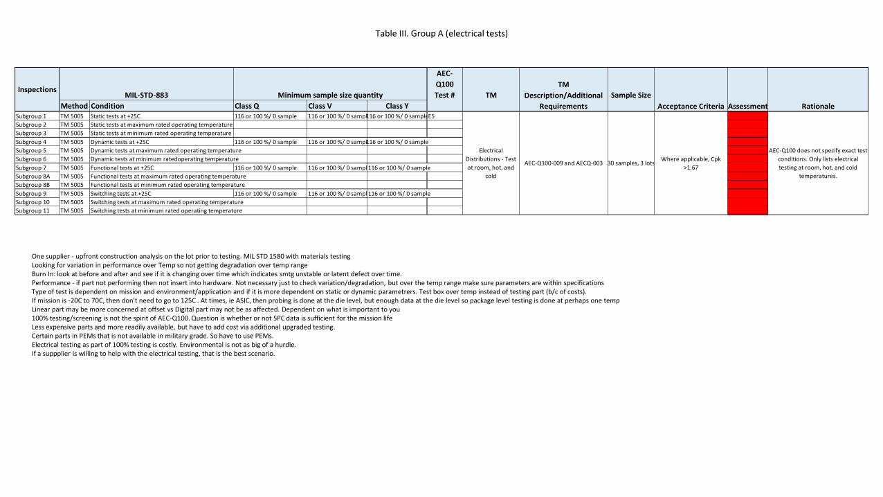
Table III. Group A (electrical tests)
AEC-Q100 Test # TM Sample Size
Method Condition Class Q Class V Class YSubgroup 1 TM 5005 Static tests at +25C 116 or 100 %/ 0 sample 116 or 100 %/ 0 sampl116 or 100 %/ 0 sampleE5Subgroup 2 TM 5005 Static tests at maximum rated operating temperatureSubgroup 3 TM 5005 Static tests at minimum rated operating temperatureSubgroup 4 TM 5005 Dynamic tests at +25C 116 or 100 %/ 0 sample 116 or 100 %/ 0 sampl116 or 100 %/ 0 sampleSubgroup 5 TM 5005 Dynamic tests at maximum rated operating temperatureSubgroup 6 TM 5005 Dynamic tests at minimum ratedoperating temperatureSubgroup 7 TM 5005 Functional tests at +25C 116 or 100 %/ 0 sample 116 or 100 %/ 0 sampl 116 or 100 %/ 0 sampleSubgroup 8A TM 5005 Functional tests at maximum rated operating temperatureSubgroup 8B TM 5005 Functional tests at minimum rated operating temperatureSubgroup 9 TM 5005 Switching tests at +25C 116 or 100 %/ 0 sample 116 or 100 %/ 0 sampl 116 or 100 %/ 0 sampleSubgroup 10 TM 5005 Switching tests at maximum rated operating temperatureSubgroup 11 TM 5005 Switching tests at minimum rated operating temperature
Acceptance Criteria Rationale
InspectionsMIL-STD-883
TM Description/Additional
RequirementsMinimum sample size quantity
Assessment
Electrical Distributions - Test at room, hot, and
cold
AEC-Q100-009 and AECQ-003 30 samples, 3 lotsWhere applicable, Cpk
>1.67
AEC-Q100 does not specify exact test conditions. Only lists electrical testing at room, hot, and cold
temperatures.
One supplier - upfront construction analysis on the lot prior to testing. MIL STD 1580 with materials testingLooking for variation in performance over Temp so not getting degradation over temp rangeBurn In: look at before and after and see if it is changing over time which indicates smtg unstable or latent defect over time.Performance - if part not performing then not insert into hardware. Not necessary just to check variation/degradation, but over the temp range make sure parameters are within specificationsType of test is dependent on mission and environment/application and if it is more dependent on static or dynamic parametrers. Test box over temp instead of testing part (b/c of costs). If mission is -20C to 70C, then don't need to go to 125C . At times, ie ASIC, then probing is done at the die level, but enough data at the die level so package level testing is done at perhaps one tempLinear part may be more concerned at offset vs Digital part may not be as affected. Dependent on what is important to you100% testing/screening is not the spirit of AEC-Q100. Question is whether or not SPC data is sufficient for the mission life Less expensive parts and more readily available, but have to add cost via additional upgraded testing.Certain parts in PEMs that is not available in military grade. So have to use PEMs. Electrical testing as part of 100% testing is costly. Environmental is not as big of a hurdle.If a suppplier is willing to help with the electrical testing, that is the best scenario.

Method (Class Q) Condition
Steady-state life testMIL-STD-883 TM 1005 J (K not available on DLA site)
1000 h at 125°C;
45 – use actual devices for lots >200 units.
5 devices or 10% of the lot, whichever is greater (for large lot <200 units). Every 3 months, unless major assembly changes
0 B2 JESD22-A1081000 h at 125°C for Grade 1; +150°C Ta for 1000 h for Grade 0
3 lots, 77 samples
1.) As noted in AEC- Q100, qualification is performed only once and maintained through SPC. An integral part of the Near Term Tech specification will need to identify all required SPC. 2.) SPC will need to be an integral part of the specification. This includes determining the independent variables such as wafer to wafer and onwafer location variablitity as well as assembly variability. These variables should be forced during sampling.
Test Conditions
A. Reverse Bias (All)B. Forward Bias (A/D)C. Power & Reverse (D/Lin)D. ParallelE. Ring oscillator
Q100-008Early Life Failure Rate SS=800; 3 lots (Can be used for production)
Thermal Derating and Appropriate biasing will need to be determined
Endurance data retention
Q100-005Thermal Derating and Appropriate biasing will need to be determined
End-point electrical parameteAs specified in the applicable device procurement specification
y p data can include sufficient SPC
InspectionsMIL-STD-883 Minimum sample
size quantityAccept number Rationale
AEC-Q100 Test # TM
TM Description/Addition
Sample Size Assessment
Table IV. Group C Life Tests
*No fails in 231 devices (77 devices from 3 lots) are applied as pass criteria for the majorenvironmental stress tests. This represents an LTPD (Lot Tolerance Percent Defective)= 1, meaning a maximum of 1% failures at 90% confidence level
*This sample size is NOT sufficient or intended for process control or PPM evaluation.Manufacturing variation failures (low ppm issues) are achieved through proper processcontrols and/or screens such as described in AEC-Q001 and AEC-Q002.
TM=detailed specs for how to bias partsrequirements for process control?

Assessment Rationale Method (Class Q) Condition Method (Class V) Condition Method (Class Y) Condition vs. Class V and Y
Subgroup 1
Physical Dimensions TM 2016 C4 Physical Dimensions JESD22-B100 and B108 and AEC-Q003
Meets intent
MIL-STD-883E TM 2016 requires measuring the package IAW case outline drawing. No other requirements on equipment calibration, accuracy or repeatability. AEC Q-100 C4 refers to JEDEC JESD22-B100B, a slightly more detailed drawing.
Lead/Terminal Integrity TM 2004 B2 (lead fatigue) or applicable for the package technology style
TM 2004 B2 (lead fatigue) or applicable for the package technology style
TM 2004 B2 (lead fatigue) or applicable for the package technology style
C6 Lead Integrity JESD22-B105
TBDAEC-Q-100 does not require this for SMD parts.
Seal Test - Fine and Gross
TM 1014 Test condition as applic TM 1014 Test condition as applicable Not applicable for class Y non-hermetic mocrocircuits devices
G4 Gross/Fine Leak TM1014
Meets intentAEC-Q-100 refers to MIL-STD-883 TM 1014. Leak tests are not applicable to PEMS devices. Moisture resistance might be a more perceptive test.
Ball Shear for BGA and Solder Column Pull Test for CGA package
BGA package: JESD22-B117 CGA package: TM 2038
BGA: 45 balls from 2 devices min.;CGA: 45 columns from 2 devices min.
BGA package: JESD22-B117 CGA package: TM 2038
BGA: 45 balls from 2 devices min.;CGA: 45 columns from 2 devices min.
BGA package: JESD22-B117 CGA package:
TM 2038
BGA: 45 balls from 2 devices min.;CGA: 45 columns from 2 devices min.
C5 Solder Ball Shear AEC-Q100-010 or AEC-Q003
Meets Intent
AEC-Q-100 specifies a Cpk and Ppk for overall ball shear and solder shear statistics for manufacturing line rather than lot by lot basis so fewer samples per lot is taken but overall line has more data points.
Thermal shock, 15 cycles TM 1011 Test condition B, 15 cyc TM 1011 Test condition B, 15 c TM 1011 Test condition B, 15 cycles min. Fails to meet intentTemperature cycling, Test Condition C 100 cycles min
TM 1010 Test condition C, 100 cycles min.
TM 1010 Test condition C, 100 cycles min.
TM 1010 Test condition C, 100 cycles min.
A5 Power temperature cycling AEC-Q-100Meets intent
These are two different tests and address different failure mechanisms. TM 1010 cycles in an electrically inactive state.
Moisture resistance TM 1004 8/ TM 1004 8/ JESD22-A118 Condition B A2, A3 Temperature/Humididty AEC-Q-100Meets or exceeds
AEC-Q-100 has more stringent flow including autoclave.
Visual examination TM 1004 or TM 1010
TM 1004 or TM 1010
TM 1004 or TM 1010 Fails to meet inten
No visual inspection TM in AEC-Q-100.
Seal Test - Fine and Gross
TM 1014 Test condition as applicable
TM 1014 Test condition as applicable
TM 1014 Test condition as a G4 Gross/Fine Leak TM1014
Meets intent
AEC-Q-100 refers to MIL-STD-883 TM 1014. Leak tests are not applicable to PEMS devices. Moisture resistance might be a more perceptive test.
End Point Electrical Parameters
As Specified As Specified As Specified AEC-Q-100 Test Group EMeets intent
Test group E includes pre and post stress parameters, electrical characteristics in addition to others such as ESD and latch up.
Mechanical shock TM 2002 Condition B minimum TM 2002 Condition B minimum TM 2002 Condition B minim G1 Mechanical Shock JESD22-B104
Meets intent
1500g peak with .5ms pulse duration is the TM2002 default test condition. AECQ-100 refers to JESD22-B104, 5 shocks per orientation, total of 30 shocks. acceleration spec range is 100g to 2900g; pulse duration range is 0.3 – 2.0ms. JESD22-B104 does not have the 1500g/.5ms default test condition.
Vibration, variable frequency
TM 2007 Condition A minimum TM 2007 Condition A minimum TM 2007 Condition A minim G2 Variable Frequency Vibration JESD22-B10320 Hz to 2 KHz to 20 Hz (logarithmic variation) in >4minutes, 4X in each orientation, 50 g peakacceleration. TEST before and after at roomtemperature.
Constant acceleration TM 2001 Test condition E, Y1 ori TM 2001 Test condition E, Y1 o TM 2001 Test condition E, Y G3 Constant Acceleration MIL STD 883, Method 2001 AEC-Q100 uses the same TM as MIL-STD-883, so the difference will be in test conditions.
Seal Test - Fine and Gross
TM 1014 Test condition as applic TM 1014 Test condition as applicable Not applicable for class Y non-hermetic mocrocircuits devices
G4 Gross/Fine Leak TM1014AEC-Q-100 refers to MIL-STD-883 TM 1014. Leak tests are not applicable to PEMS devices. Moisture resistance might be a more perceptive test.
Visual examination TM 2007 TM 2007 TM 2007 This test does not exist in AEC Q-100.End Point Electrical Parameters
As Specified As Specified As Specified AEC-Q-100 Test Group ETest group E includes pre and post stress parameters, electrical characteristics in addition to others such as ESD and latch up.
Salt atmosphere TM 1009 Test condition A, minimum
TM 1009 Test condition A, minimum
TM 1009 Test condition A, minimum
Visual examination TM 1009 TM 1009 TM 1009Seal Test - Fine and Gross
TM 1014 Test condition as applicable
TM 1014 Test condition as applicable
Not applicable for class Y non-hermetic mocrocircuits devices
G4 Gross/Fine Leak TM1014AEC-Q-100 refers to MIL-STD-883 TM 1014. Leak tests are not applicable to PEMS devices. Moisture resistance might be a more perceptive test.
Subgroup 6
Internal water vapor test (cavity packages) - 5000 ppm max at 100C
TM 1018 3 (0) samples, 5000 ppm max water content at 100°C
TM 1018 3 (0) samples, 5000 ppm max water content at 100°C
Not applicable for class Y non-hermetic mocrocircuits devices
G8 Internal Water Vapor MIL STD 883, Method 1018MIL-STD-883 TM 1018; AEC-Q-100 uses the same TM, no differences except those of detailed failure definitions.
Subgroup 7 Adhesion of lead finish TM 2025 Where applicable TM 2025 Where applicable TM 2025 Where applicable No method in AEC-Q-100
Subgroup 8Lid Torque TM 2024 Where applicable TM 2024 Where applicable TM 2024 Where applicable G6 Lid Torque MIL STD 883, Method 2024 MIL-STD-883 TM 2024; AEC-Q-100 uses the
same TM, no differences except those of detailed failure definitions.
Soldering heat TM 2036 Where applicable TM 2036 Where applicable TM 2036 Where applicable No method in AEC-Q-100Seal Test - Fine and Gross
TM 1014 Where applicable TM 1014 Where applicable TM 1014 Where applicable G4 Gross/Fine Leak TM1014 AEC-Q-100 refers to MIL-STD-883 TM 1014. Leak tests are not applicable to PEMS devices. Moisture resistance might be a more perceptive test.
Visual examination TM 2009 TM 2009 TM 2009 No visual inspection TM in AEC-Q-100.End Point Electrical Parameters
As Specified As Specified As Specified AEC-Q-100 Test Group ETest group E includes pre and post stress parameters, electrical characteristics in addition to others such as ESD and latch up.
Subgroup ? G5 Package Drop No package drop test in MIL-STD-883
Subgroup ?Die shear TM2019 G7 Die Shear MIL STD 883, Method 2019 AEC-Q100 uses the same TM as MIL-STD-
883, so the difference will be in test conditions.
Subgroup 3
Subgroup 4
Subgroup 5
Subgroup 9
MIL-STD-883 MIL-STD-883 TM Description/Additional Requirements
Subgroup 2
Subgroup Tests TestsMIL-STD-883
AEC-Q100 Test # TM
Table V. Group D Tests (Package related tests)
The Assessment column would contain one of four colorsBlue = AEC requirement fully meets or exceeds that of MIL-PRF-38535Green = Meets Intent of MIL-PRF-38535 (test may be different, but tests for same failure mechanism)Yellow = Partially Meets Intent of MIL-PRF-38535.Red = Fails to Meet Intent of MIL-PRF-38535.Gray = Not applicable for short term mission payloads.

MIL-PRF-19500 vs. AEC-Q101Semiconductor DevicesSong Pyun (Raytheon)
Table E-IV. Screening Requirements
Method ConditionDie visual for glassdiodes
2073Condition B, die form prior to assembly
100% NA NA Not specified No requirements in AEC-Q101
Internal visual (pre-cap) inspection: For diodes For power FETs For microwave transistors For transistors
2074206920702072
100% 100% NA Not specified No requirements in AEC-Q101
High Temp life (non operating life) (stabilization bake)
1032
Less than or equal to maximum rated storage temperature, t = as specified (340 h min, unless specified)
Optional Optional Optional Not specified No requirements in AEC-Q101
Temperature Cycling 1051
20 cycles. No dwell time is required at +25°C. Test condition C (-55 to 175°C) or maximum storage temperature, whichever is less.
100% 100% 100% JESD22-A104
1000 cycles (-55°C to max rated junction T, not
to exceed 150°C). Reduce to 400 cycles (25°C over part max
rated junction T or 175°C if rated >150°C). No
100% Screening, Initial Qualification only
3 lots77 samples each
Only performed for qual. Similar temperature ranges
Surge 4066Condition A (sinusoidal current surge) or B (rectangular current phase), as specified
100% 100% 100% Not specified No requirements in AEC-Q101
Thermal Impedance Transistors, Power FETs Bipolar Diodes IGBT GaAs FET
31613131310131033104
As specified 100% 100% 100%JESD24-3JESD24-4JESD24-6
No 100% Screening, Initial Qualification only
1 lot10 samples each
for pre- and post-change
Test to assure specification compliance and provide
process change comparison data
Constant acceleration. Not required for stud devices and metallugically bonded diodes.
2006
Y1 direction at 20,000 G minimum, except at 10,000 G minimum for devices with power rating of ≥10 watts at TC = +25°C. The 1 minute hold time requirement shall not apply.
100% Optional OptionalMIL-STD-750, Method 2006
Y1 plane only, 15K g-force. Test before and
after CA. No 100% Screening, Initial
Qualification only
1 lot30 samples
Lower g-force. Only perrformed for qual.
PIND 2052Condition A (20 g's peak at 40-250 Hz) or B (10 g's peak at 60 Hz minimum), as specified
100% NA NA Not specified No requirements in AEC-Q101
Instability shock test (axial lead diodes only) FIST BIST
20812082
100% NA NA Not specified No requirements in AEC-Q101
Hermetic Seal Fine Gross
1071Fine leak not required for double plug diodes.
Optional Optional OptionalJESD22A-109
Fine and gross leak test per individual user
specification1 Lot 30 parts
Serialization 100% 100% 100% Not specified No requirements in AEC-Q101
Interim electrical parameters As specified 100% (read and record)For case mounted
rectifiers as specifiedFor case mounted
rectifiers as specified
User specification or supplier’s
standard specification
As needed for pre- and post-stress electrical test
All qualification parts submitted
for testing
High temperature reverse bias (HTRB): For Transistors
For power FETs
For diodes and rectifiers
1039
1042
1038
Test condition A (steady-state reverse bias): 80 percent (minimum) of rated VCB (bipolar), VGS(FET), or VDS(FET), as applicable.
Test condition B:80 percent (minimum) of rated VGS
Test condition A: Diodes (not required for LEDs, Zeners, and case mounted rectifiers) 80% minimum of rated VR or VRWM when DC conditions are specified. 95 - 100% of VRWM, when half sine condition is specified.
100% 100% 100%MIL-STD-750, Method 1038
1000 h at max DC Reverse Voltage rated junction T. No 100%
Screening, Initial Qualification only
3 lots77 samples each
Method 1038 is only for diodes, rectifiers, and zeners.
Testing methods for transistors and power FETs
not specified in AEC.
Interim electrical and delta parameter for PDA
As specified but including all delta parameters as a minimum. When HTRB is performed leakage current shall be measured on each device before any other specified parametric test is made.
100-percent (Measure all specified
parameters. Measure leakage current within 16 hours after removal
of applied voltage in HTRB. Record those
parameters which have a delta limit.) (See
screen 13 of table EIV.)
100-percent (Measure all specified
parameters. Measure leakage current within 24 hours after removal
of applied voltage in HTRB. Record those
Parameters which have a delta limit.) (See
screen 13 of table EIV.)
100-percent (Measure all specified parameters.
Measure leakage current within 24 hours after
removal of applied voltage in HTRB. Record those Parameters which have a delta limit.) (See screen 13 of table E-IV.)
User specification or supplier’s
standard specification
As needed for pre- and post-stress electrical test
(no PDA)
All qualification parts submitted
for testing
Burn in for: Bipolar Transistors Power FETs Diodes, Zeners, and rectifiers Case mount rectifiers
Thyristors Bipolar small die transistors Bipolar power transistors
103910421038
104010391039
Test condition BTest condition ATest condition BCondition A (HTRB), JANTX and JANTXV onlyCondition B, for JANS
Condition BCondition B
100-percent240 hours (minimum)240 hours (minimum)240 hours (minimum)
Not applicable240 hours (minimum)240 hours (minimum)240 hours (minimum)240 hours (minimum)
100-percent160 hours (minimum) 160 hours (minimum)96 hours (minimum)48 hours (minimum)
Not applicable96 hours (minimum)
160 hours (minimum)160 hours (minimum)
100-percent160 hours (minimum) 160 hours (minimum)96 hours (minimum)48 hours (minimum)
Not applicable96 hours (minimum)
160 hours (minimum)160 hours (minimum)
MIL-STD-750, Method 1038Method 1040
1000 h at max DC Reverse Voltage rated
junction T. 1000 h at max AC blocking voltage and
junction T. No 100% Screening, Initial
Qualification only
3 lots - 77 samples each
Final electrical test Interim electrical and delta parameters for PDA
Other electrical parameters
As specified
100-percent Group A, subgroup 2, interim electrical and delta
parameters. (read and record)
Group A, subgroup 3
100-percent Group A, subgroup 2. Read and
record interim electrical and delta parameters
Not applicable
100-percent Group A, subgroup 2. Read and
record interim electrical and delta parameters
(see
Not applicable
User specification or supplier’s
standard specification
As needed for pre- and post-stress electrical test
(no PDA)
All qualification parts submitted
for testing
Hermetic Seal Fine Gross
1071 Omit for double plug diodes 100% 100% 100%JESD22A-109
Fine and gross leak test per individual user
specification1 Lot 30 parts
Radiography 2076 Detect defects within sealed cases 100% Not Applicable Not Applicable Not specified No requirements in AEC-Q101
External visual examination 2071To be performed after complete marking and prior to lot acceptance.
100% Not Applicable Not Applicable JESD22-B101No 100% Screening,
Initial Qualification only
All qualification parts submitted
for testing
Case Isolation 1081To be performed on all case isolated packages, as specified.
100% 100% 100% Not specified No requirements in AEC-Q101
Sample Size Assessment RationaleTM
Description/Additional TMMIL-STD-750
Inspection JANS JANTXV JANTX

MIL-PRF-19500 vs. AEC-Q101Semiconductor DevicesSong Pyun (Raytheon)
Table E-VIA Group B Inspections for JANS devices
Method ConditionSubgroup 1
Physical dimensions2066
Dimensions in accordance with case outline specified in specification sheets.
22 devices, c = 0 8 devices, c = 0 JESD22 B-100 Part of Initial Qualification 1 lot, 30 samples
Subgroup 2
Solderability 2026The sample plan applies to the number of leads inspected. A minimum of three devices shall be tested.
15 leads, c = 0 6 leads, c = 0J-STD-002JESD22-B102
Part of Initial Qualification 1 lot, 10 samples Lower quantity in AEC
Resistance to Solvents 1022Ink marked devices only. Not required if marking is etched into the device.
15 devices, c = 0 6 devices, c = 0 JESD22-B107 Part of Initial Qualification 1 lot, 30 samples
Salt Atmosphere (corrosion) 1041
Salt atmosphere at +35°C passed thru chamber for 24 +2/-0 h at rates of 10 - 50 g/m^2 per 24 h; examine post test. Laser marked devices only. Not required for non-corrrosive base metals.
6 devices, c = 0 6 devices, c = 0 Not specified No requirements in AEC-Q101
Subgroup 3Thermal shock (liquid-to-liquid)
1056 25 cycles, condition B (glass diodes only) Not specified No requirements in AEC-Q101
Temperature cycling(air-to-air) 1051
Test condition C, or maximum storage temperature, whichever is less. (100 cycles).
JESD22-A104 Part of Initial Qualification3 lots, 77 samples each
Surge 4066 As specified. Not specified No requirements in AEC-Q101Hermetic seal Fine Gross
1071Fine leak not required for double plug diodes.
JESD22A-109
Fine and gross leak test per individual user specification
1 Lot 30 parts
Electrical Measurements Group A, subgroup 2
User specification or supplier’s standard specification
As needed for pre- and post-stress electrical test
All qualification parts submitted for testing
Decap-internal visual (design verification)
2075Visual criteria in accordance with qualified design and internal visual precap criteria.
6 devices, c = 0 6 devices, c = 0 Not specified No requirements in AEC-Q101
Bond strength(wire or clip bonded devices only)
2037
Condition D: testing for internal bonds at the die or substrate and the lead frame. Similar to Condition C, but uses a hook under the lead wire.
22 wires or 11 devices, c = 0, (whichever requires the smaller number of devices.)
12 wires or 6 devices, c=0 (whichever requires the smaller number of devices.)
MIL-STD-750, Method 2037
500 h, T_A = max rated T_j for bonding of dissimilar metals, decap and wire pull/bond inspection after WBI on all wires.
10 bonds from min of 5 parts
Same as wire bond integrity in AEC?
SEM for applicabledesigns)
2077 Not specified No requirements in AEC-Q101
Die shear (excluding axial leaded devices)
2017
The same number of devices used for bond strength will also beused for die shear (minimum of six die).
MIL-STD-750, Method 2017
Not specified 1 lot, 5 samples Lower quantity in AEC
Subgroup 4
Intermittent operation life1037 or
1042
2,000 cycles, Condition D. Devices with .008 inch or larger bond wires, 6,000 cycles.
MIL-STD-750, Method 1037
Part of Initial Qualification3 lots, 77 samples each
Hermetic seal Fine Gross
1071Fine leak not required for double plug diodes.
JESD22A-109
Fine and gross leak test per individual user specification
1 Lot 30 parts
Electricalmeasurements
Group A, subgroup 2 and as specified.
User specification or supplier’s standard specification
As needed for pre- and post-stress electrical test
All qualification parts submitted for testing
Bond strength(wire or clip bondeddevices only)
2037Condition D. The sample shall include a minimum of three devices and shall include all wire sizes.
11 wires, c = 0 11 wires, c = 0MIL-STD-750, Method 2037
Part of Qualification10 bonds from min of 5 parts
Same as wire bond integrity in AEC?
Subgroup 5
Accelerated steady-state operation life
1027
Bias conditions as specified.
TJ = +275°C minimum (for 96 hours minimum) or TJ = +225°C minimum (for 216 hours minimum) or TJ = rated °C minimum (for 1,000 hours minimum).
Not specified No requirements in AEC-Q101
Electricalmeasurements
Group A, subgroup 2 and 3
User specification or supplier’s standard specification
As needed for pre- and post-stress electrical test
All qualification parts submitted for testing
Schottky diodes, Casemount rectifiers
1038TJ = rated TJ maximum(for 1,000 hours minimum).
MIL-STD-750, Method 1038
Part of Qualification3 lots77 samples each
Electricalmeasurements
Group A, subgroup 2 and 3.
User specification or supplier’s standard specification
As needed for pre- and post-stress electrical test
All qualification parts submitted for testing
Accelerated steadystategate stresspower MOSFETS
1042
Condition B,VGS = rated, TA = +175°C,t = 24 hours or TA = 150°C,t = 48 hours.
JESD22-A108 Part of Qualification3 lots77 samples each
Electricalmeasurements
Group A, subgroup 2 and 3.
User specification or supplier’s standard specification
As needed for pre- and post-stress electrical test
All qualification parts submitted for testing
Accelerated steady-statereverse biaspower MOSFETS
1042
Condition A,VDS = rated, TA = +175°C,t = 120 hours or TA = 150°C,t = 240 hours and asspecified.
JESD22-A108 Part of Qualification3 lots77 samples each
Electricalmeasurements
Group A, subgroup 2 and 3.
User specification or supplier’s standard specification
As needed for pre- and post-stress electrical test
All qualification parts submitted for testing
Bond strength(wire or clip bonded devices only)
2037As specified. Bond strength samples shall have passed accelerated steady-state operation life.
20 wires, c = 0 20 wires, c = 0MIL-STD-750, Method 2037
Part of Qualification10 bonds from min of 5 parts
Same as wire bond integrity in AEC?
Subgroup 6Thermal resistanceDiodes 3101 or 4081 Not specified No requirements in AEC-Q101Transistors (bipolar) 3131 JESD24-4 Part of Qualification 1 lot, 10 samples Lower quantity in AECTransistors (POWER FETS) 3161 JESD24-3 Part of Qualification 1 lot, 10 samples Lower quantity in AECThyristors 3181 Not specified No requirements in AEC-Q101IGBT 3103 JESD24-6 Part of Qualification 1 lot, 10 samples Lower quantity in AECGaAs FET 3104 Not specified No requirements in AEC-Q101
Subgroup 7High temperature life (non-operating)
340 hours minimum, T_STG(max) = T_A Not specified No requirements in AEC-Q101
Electrical Measurements Group A, subgroup 2
User specification or supplier’sstandard specification
As needed for pre- and post-stress electrical test
All qualification parts submitted for testing
1032 32 devices, c = 012 devices
c = 0
Qualification and Large Lot Conformance
Small Lot Conformance Inspection
MIL-STD-750
As specified. Thermal resistance may beperformed on a group C frequency whenever 100% thermal impedance is performed, except for power and case mounted devices
22 devices, c = 08 devices
c = 0
Separate samples may be used for each test.
TM Sample Size Assessment RationaleTM Description/Additional
RequirementsInspections
22 devices, c = 0 6 devices, c = 0
See MIL-STD-750 TM 2077 for details.
22 devices, c = 012 devices
c = 0
22 devices, c = 012 devices
c = 0

MIL-PRF-19500 vs. AEC-Q101Semiconductor DevicesSong Pyun (Raytheon)
Table E-VIB Group B Inspections for JAN, JANTX, and JANTXV devices
Method ConditionSubgroup 1
Solderability 2026
The sample plan applies to the number of leads inspected. A minimum of 3devices shall be tested.
15 leadsc = 0
4 leadsc = 0
J-STD-002JESD22-B102
Part of Qualification1 lot
10 samplesLower quantity in AEC
Resistance to Solvents 1022Not required if marking is etched into the device.
15 leadsc = 0
3 leadsc = 0
JESD22-B107 Part of Qualification1 lot
30 samplesSubgroup 2
Thermal Shock (liquid to liquid) 105610 cycles, condition B, (glass diodes only).
Not specified No requirements in AEC-Q101
Temperature Cycling (air to air) 1051
Test condition C, or maximum storage temperature, whichever is less. (45 cycles including screening)
JESD22-A104 Part of Qualification3 lots
77 samples each
Surge 4066 As specified. Not specified No requirements in AEC-Q101
Salt atmosphere (corrosion) 1041
Salt atmosphere at +35°C passed thru chamber for 24 +2/-0 h at rates of 10 - 50 g/m^2 per 24 h; examine post test. Laser marked devices only.
Not specified No requirements in AEC-Q101
Hermetic seal Fine Gross
1071Fine leak not required for double plug diode.
Not specified No requirements in AEC-Q101
Electrical Measurements Group A, subgroup 2
User specification or supplier’sstandard specification
As needed for pre- and post-stress
electrical test
All qualification parts submitted
for testing
Subgroup 3
Steady-state operation life 1027Bias conditions as specified, 340 hours (minimum)
Not specified No requirements in AEC-Q101
Electrical measurements orIntermittent operation life
1037
1042
Group A, subgroup 22,000 cycles (min)Condition D, 2,000 cycles (min)
MIL-STD-750, Method 1037
T_J >100°C: 60000/(x+y), 15000
cyclesT_J >125°C:
30000/(x+y), 7500 cycles
3 lots77 samples each
Hermetic seal Fine Gross
1071Fine leak not required for double plug diodes.
JESD22A-109
Fine and gross leak test per individual user specification
1 Lot 30 parts Lower quantity in AEC
Electrical measurements Group A, subgroup 2
User specification or supplier’sstandard specification
As needed for pre- and post-stress
electrical test
All qualification parts submitted
for testing
Bond strength (wire or clip bonded devices only)
2037
Condition D. The sample shall include a minimum of three device and shall include all wire sizes.
11 wiresc = 0
11 wiresc = 0
MIL-STD-750, Method 2037
Part of Qualification10 bonds
from min of5 parts
Subgroup 4
Decap internal visual (design verification)
2075Visual criteria in accordance withqualified design.
1 devicec = 0
1 devicec = 0
Not specified No requirements in AEC-Q101
Subgroup 5Thermal resistanceDiodes 4081 Not specified No requirements in AEC-Q101
Transistors (bipolar) 3131 JESD24-4 Part of Qualification1 lot
10 samplesLower quantity in AEC
Transistors (POWER FETS) 3161 JESD24-3 Part of Qualification1 lot
10 samplesLower quantity in AEC
Thyristors 3181 Not specified No requirements in AEC-Q101
IGBT 3103 JESD24-6 Part of Qualification1 lot
10 samplesLower quantity in AEC
GaAs FET 3104 Not specified No requirements in AEC-Q101Subgroup 6
High-temperature life(non-operating)
Not specified No requirements in AEC-Q101
Electrical measurements
User specification or supplier’s standard specification
As needed for pre- and post-stress
electrical test
All qualification parts submitted
for testing
1032340 hours minimum, TSTG(max) = TAGroup A, subgroup 2
32 devices, c = 0 12 devices, c = 0
MIL-STD-750
As specified. Thermal resistance maybe performed on group C frequency whenever 100% thermal impedance is performedexcept for power and case mounted devices.
15 devicesc = 0
6 devicesc = 0
45 devicesc = 0
45 devices, c = 0
22 devicesc = 0
6 devicesc = 0
TMInspectionQualification and
Large Lot Small Lot Conformance
InspectionTM
Description/Additiona Sample Size Assessment RationaleSeparate samples may be used for each test

MIL-PRF-19500 vs. AEC-Q101Semiconductor DevicesBill Cantarini (HiRel Components Engineering & Manufacturing)
Group A Inspection
Method ConditionSubgroup 1 (all devices except small die flow)
Visual and mechanical inspection
2071Verify workmanship of hermetically packaged semiconductor devices
15 devicesc = 0
116 devices, c = 0(JANTXV)
45 devices, c = 0(JAN, JANTX)
JESD22 B-101inspect part construction, marking
and workmanship1 lot
30 samples
Qty higher than JANS, but JANS devices are
manufactured to higher standards.
Subgroup 1 (for small die flow only 2/ 3/)
Visual and mechanical inspection 4/
2071Verify workmanship of hermetically packaged semiconductor devices
116 devices, c = 0(JANTXV)
45 devices, c = 0(JAN, JANTX)
JESD22 B-101inspect part construction, marking
and workmanship1 lot
30 samplesLower quantity in AEC
Solderability 4/2026
(J-STD-002)
15 leads, c = 0J-STD-002
JESD22B102
Magnification 50x. Reference solder conditions in Table 2B. Apply test
method A for through-hole, or both test methods B and D for SMD.
1 lot10 samples
Lower quantity in AEC
Resistance to solvents 4/ 5/ 1022
Verify that the markings will not become illegible on devices when subjected to solvents.
15 devices, c = 0 JESD22-B107Verify marking permanency (not
required for laser etched parts or parts with no marking)
1 lot30 samples
Salt Atmosphere (corrosion), (Laser marked devices only. Not required
for non-corrosive base metals)
1041
Salt atmosphere at +35°C passed thru chamber for 24 +2/-0 h at rates of 10 - 50 g/m^2 per 24 h; examine post test.
6 devices, c = 0Salt not listed but Autoclave
and Corrosion are referenced
Temperature cycling (air to air)
1051
Default test conditions: minimum of 20 cycles using test condition C (-55 to 175°C).
Test condition C, or maximum storage temperature, whichever is
less, 25 cycles. 22 devices, c = 0
JESD22 A-104, Appendix 6
1000 cycles (Ta = minimum range of -55°C to maximum rated junction
temperature, not to exceed 150°C). Can reduce duration to 400 cycles
using Ta (max) = 25°C over part maximum rated junction
tempreature or using Ta(max) = 175°C if the maximum rated junction
tempreature is above 150*C. Test before and after TC
3 lots77 samples
each
Electrical measurements (group A, subgroup 2)
Group A, subgroup
2
User specification or
supplier’sstandard
specification
All qualification parts submitted
for testing
Hermetic seal 6/
Fine leakGross leak
Bond strength 4/ 2037Precondition: Ta = +250°C at t = 24
h or Ta = +300°C at t = 2 h; 11 wires, c = 0
MIL-STD-750 Method 2037
Pre- & post-process change comparison to evaluate process
change robustness
10 bondsfrom min of
5 parts
Decap internal visual (design verification)
2075
Verify that design and construction of dvice are the same as those documented in qualified design report.
4 devices, c = 0AEC-Q101-004, Section 4 (DPA)
Random sample of parts that have successfully completed H3TRB or
HAST, and TC2 samples, 1 lot Only DPA specified.
Subgroup 2
DC (static) test +25°C ± 3°C 116 devices c = 0 7/ 9/ 116 devices c = 0 7/
User specification or
supplier's standard
specification
Test is performed as specified in the applicable stress reference at room
temperature
3 Qual lots 77parts/lot
Subgroup 3
DC (static) testHigh (-0°C, +10°C) and low (+0°C, -10°C) specified temperatures
116 devices c = 0 7/ 9/ 116 devices c = 0 7/ 8/
User specification or
supplier's standard
specification
Test is performed as specified in the applicable stress reference at room
temperature
All qualification parts submitted
for testing
No temperature testing stated in specifications
Subgroup 4
Dynamic tests +25°C ± 3°C 116 devices c = 0 7/ 9/ 116 devices c = 0 7/ 8/
User specification or
supplier's standard
specification
Test is performed as specified in the applicable stress reference at room
temperature
All qualification parts submitted
for testingNote 1
Subgroup 5Safe operating area test
(for transistors only):a. DC
b. Clamped inductive (only when applicable)
End-point electrical measurements
45 devices c = 0 Note 2
Safe operating area test c. Unclamped inductive (only when applicable)
End-point electrical measurements
45 devices c = 0AEC-Q101-004
Section 2
Pre- & Post-process change comparison to evaluate
process change robustness (Power MOS and internally clamped IGBTs
only).
1 lot 5 samples See Table 2 Item 26
Subgroup 6Surge current (for
diodes/rectifiers only)
End-point electrical measurements
22 devices c = 0
User specification or
supplier's standard
specification
Surge not referenced in AEC100All qualification parts submitted
for testingNote 2
Subgroup 7
Selected static and dynamic tests
45 devices c = 0 10/ 22 devices c = 0
User specification or
supplier's standard
specification
As needed for pre- and post-stress electrical test (no PDA)
All qualification parts submitted
for testing
MIL-PRF does not specify tests and is assignable by the
customer similar to AEC-Q101
Subgroups
45 devices c = 0 10/
Assessment Rationale
MIL-STD-750
JANS sample plan
1071 22 devices, c = 0
JAN, JANTX, JANTX sample plan
TM
Refer to page 12JESD22A-109
1 Lot 30 parts
TM Description/Additional Requirements
Sample
Fine leak not required for double plug diodes.
Fine and gross leak test per individual user specification
1) As noted in AEC- Q100, qualifiation is performed only once and maintained through SPC. An integral part of the Near Term Tech specification will need to identify all required SPC.2) SPC will need to be an integral part of the specification. This includes determining the independent variables such as wafer to wafer and onwafer location variablitity as well as assembly variability. These variables should be forced during sampling.
Note 1 - Under AEC101 Apendix 5 "Minimum Parametric Test" there is no listing for SOA testsNote 2- Under AEC101 Apendix 5 "Minimum Parametric Test" there is no listing for Surge tests

MIL-PRF-19500 vs. AEC-Q101Semiconductor DevicesSultan Lilani (Integra Technologies)
Group C Periodic Inspections (all quality levels)
Tab: Table E-VII
Method ConditionSubgroup 1
Physical dimensions 1/(not required for JANS)
2066Dimensions in accordance with case
outline specified in specification sheets
15 devices c=0
6 devices c=0 JESD22 B-100
Verify physical dimensions to the applicable user part
packaging specification for dimensions and tolerances
Note 1: For AEC; performed during initial qual or when
process change is made
Subgroup 2
Thermal Shock (liquid to liquid)
1056 25 cycles, condition B Not stated in AEC-Q101
Temperature cycling (air-to-air)
1051
Test condition C (-55 to +175°C), or maximum storage temperature,
whichever is less. (45 cycles including screening)
JESD22 A-104, Appendix 6
1000 cycles (TA = minimum range of -55°C to maximumrated junction temperature,
not to exceed 150°C). Canreduce duration to 400 cycles
using TA (max) = 25°C overpart maximum rated junction temperature or using TA(max)= 175°C if the maximum rated
junction temperature isabove 150°C. TEST before and after TC. Note: AEC additional req't is post temp cycle: 125°C
TEST after TC, followed by decap and wire pull on
all wires from 5 devices per appendix 6 for parts with
internal bond wire sizes 5 mil diameter and less. In addition, there is 100% CSAM req't post
TC.
77 samples from 3 lots for each test
AEC requires more cycles, along with pre- and post-test
inspections.
Terminal strength 2036 As specified MIL-STD-750, Method 2036Evaluate lead integrity of
leaded parts only
Surface mount end cap bond integrity
2038As specified (Condition B for US
devices)AEC-Q101, Appendix 6
Guideline for opening plastic packaged devices for reliable
wire pull or bond shear testing.
AEC-Q101 Appendix 6 refers to plastic parts only. No specifics on
end cap bond integrity testing.
Hermetic seal 2/
a. Fine leakb. Gross leak
Moisture resistance 1021 Omit initial conditioning
AEC has no provision for moisture resistance testing for
hermetic package but does perform HAST with
preconditioning for plastic Electrical measurements
Group A, subgroup 2
Subgroup 3
Shock 2016
Nonoperating, 1,500 G's, 0.5 ms, 5 blows in each orientation, X1, Y1,
and Z1 (Y1 only for axial glass diodes)
JESD22 B-1041500 G's for 0.5 ms, 5 blows, 3 orientations. Test before and
after mechanical shock
Vibration, variable frequency
2056
Peak-to-peak amplitude of 0.06" or peak accleereation of 20 g's over 20 to 2000 Hz; Cycle performed 4 times
in each x, y, and z orientations.
JESD22 B-103
Use a constant displacement of 0.06" (double amplitude)
over the range of 20 Hz to 100 Hz and a 50 G constant peak
acceleration over the range of 100 Hz to 2 KHz. Test before
and after VVF
Constant accleration 3/ 2006
1 minute minimum in each orientation. X1, Y1, and Z1 at 20,000 G's minimum, except at 10,000 G's minimum for devices with power
rating of ≥ 10 watts. Tc = +25°C
MIL-STD-750, Method 2006Y1 plane only, 15K G-force.
Test before and after constant acceleration
30 samples, 1 lotAEC requires Y1 plane only, 15K g-
force
Electrical measurements
Group A, subgroup 2
Subgroup 4
Salt atmosphere (corrosion) 1/
1041
Salt atmosphere at +35°C passed thru chamber for 24 +2/-0 h at rates of 10 - 50 g/m^2 per 24 h; examine
post test
15 devices c=0
6 devices c=0 Not stated in AEC-Q101
Subgroup 5Thermal resistance 4/Diodes 4081Transistors (bipolar) 3131Transistors (power FETs)
3161
Thyristors 3181IGBT 3103CaAs FET 3104
Subgroup 6 5/ 6/
Steady-state operation life
10261,000 hours minimum, bias
conditions as specified. 7/ 8/
Test methods as follows corresponding to each test in column F: HTRB: -STD-750-1 M1038 Method A, AC blocking voltage: MIL-STD-750-1 M1040 Test condition A, HTFB: JESD22 A-108, Steady state: MIL-STD-750-1 M1038 Condition B (Zeners), HTGB: JESD22 A-108
1000 hours for each of the following tests are performed with testing before and after
each hrs of each of the following: HTRB (reverse bias),
AC blocking voltage, HTFB (forward bias), Steady state
operational , HTGB (gate bias)
77 samples from 3 lots for each test
Electrical measurements or Intermittent operation life
1037 6,000 cycles minimum MIL-STD-750, Method 1037
Intermittent operational life: Tested per duration indicated
in Table 2A. Ta=25°C. Parts powered to insure
△
Tj ≥ 100°C (not to exceed absolute
maximum ratings). Test before and after IOL as a minimum
Sample size not specified in AEC.
Hermetic seal 2/
a. Fine leakFine leak not required for double
plug diodesb. Gross leakElectrical measurements
Group A, subgroup 2
Bond strength 9/ 2037
Condition D, .008 inch or larger wire or clip bonded devices only. The
sample shall include a minimum of three devices and shall include all
wire sizes
MIL-STD-750, Method 2037Pre- and post-process change
comparison to evaluate process change robustness
or Blocking life 8/ 1048
Perform with primary blocking junction reverse biased at elevated T
for time period in accordance with life test requirements. Typically +150°C and at 80-85% of rated
voltage.
This test methodology is not addressed in AEC document.
Alternative method (steady state or intermittent life; may be used
with revised biasing scheme)
Electrical measurements
Group A, subgroup 2
Additional AEC-Q101 test include : Unbiased HAST, biased HAST, High humidity High temp forward bias, High humidity, high temp reverse bias,
Subgroup 7 10/
Internal gas analysis 1018To be performed on each
structurally identical package family3 devices c=0
3 devices c=0
This test methodology is not addressed in AEC document. This
is an important test and should be performed
Sample size not specified in AEC.
1071JESD22 B-109
Fine and gross leak test per individual user specification
Sample size not specified in AEC.
11 wires, c=0
11 wires, c=0
As specified
MIL-STD-750
22 devices
c=06 devices c=0
22 devices
c=012 devices c=0
6 devices c=0
Not required for disc packages or metallurgically bonded double plug devices or stud packaged devices
JESD22 A-109 1 Lot 30 parts
Sample Plan
Small lot conformance
inspectionInspections
1071Fine leak not required for double
plug diodes.
22
Sample Size RationaleTM Description/Additional Requirements
AssessmentTM
Fine and gross leak test per individual user specification
15 devices
c=06 devices c=0
Not required for disc packages
JESD24-3, 24-4, 24-6 as appropriate
Measure TR to assure specification compliance and
provice process change comparison data
1/ Electrical reject devices, from the same inspection lot, may be used for all subgroups when electrical end-point measurements are not required. Other non-catastrophic rejected devices (i.e., PIND, X-ray) may be utilized for all subgroups. For subgroups with end-point measurements, the devices shall be screened to table E-IV through screen 13. Salt atmosphere not required for Laser marked devices when devices from group B, or from group A for small die flow, salt atmosphere have been selected to satisfy group C inspection requirements.
2/ Non-transparent glass encased double plug noncavity diodes only may use test method 2068 of MIL-STD-750, in lieu of 1071. This test may be performed after electrical measurements.
3/ Not applicable to any devices with external and internal pressure contacts (die to electrical contacts), optical coupled isolators, and double plug diodes.
4/ Not required when performed in group B.
5/ If a given inspection lot undergoing group B inspection has been selected to satisfy group C inspection requirements, the 340 hour or 2,000 cycles life tests may be continued on test to 1,000 hours or 6,000 cycles, as applicable, in order to satisfy the group C life test requirements. End-point measurements shall be performed on either table E-VIA, group B, subgroup 4, or table E-VIB group B, subgroup 3 (340 hours or 2,000 cycles, as applicable) to satisfy group B (table E-VIA or table E-VIB) lot acceptance or group C, subgroup 6 (1,000 hours or 6,000 cycles, as applicable) to satisfy group B and C lot acceptance.
6/ Intermittent operation life shall be performed on all case mounted devices.
7/ TJ = 150°C (min) or rated TJ whichever is less (except schottky and power mosfets) for operation life.
8/ The sample size may be increased and the test time decreased so long as the devices are stressed for a total of 22,000 device hours minimum, and the actual time of test is at least 340 hours.
9/ Required for JANS devices with .008 inch or larger bond wires only. Not required when JANS devices from group B bond pull inspection have been selected to satisfy group C inspection requirements.
10/ Internal gas analysis shall be performed on hermetic devices. An engineering evaluation shall be performed if there is a device failure to determine the moisture source (e.g. sealing environment, non hermetic device). The entire lot shall be rescreened in accordance with screen 14 herein (and resubmitted at 6/0.) Corrective action shall be taken as necessary. Subgroup 7 is not required for noncavity double plug devices.
"- I had some time today so I took a look at the Mil-PRF-19500 table comparison. It looks like someone started working on it so I didn’t add to the already filled columns. However, I added a column next to automotive test method with sample size. Hope it is okay. I figured it gives an idea on automotive sampling required since their qual methodology is very different from Mil standard.
- I added some req’ts to Table E-VII for steady state life, constant acceleration sample and Temp cycle.AEC-Q101 adds several types of 1000 hr life testing (not just one per Mil-PRF-19500). See table above.AEC-Q101 adds several biased HAST and CSAM following temp cycle (I noted them in table).
- Some general notes are same as notes on Mil-PRF-38535.o Group A and Group B of Mil-PRF-19500 do not have an equivalent AEC-Q101.o Qualification is performed initially with no repeats unless a process changes.o A couple of tests, ie. ESD and parametric are required for each new part but other tests called out in AEC-Q101 can be applied to part family.ThanksLilian"

MIL-PRF-123 vs. AEC-Q200Capacitors, fixed, ceramic dielectric
Table IX. Qualification Inspection
TM TM DescriptionNumber of sample units to be inspected
Number of failures 1/
TM TM Description/Additional Requirements
Sample Size per Lot
Number of lots
Assessment Rationale
Group IRadiographic inspection (leaded devices only) 4.6.5 All N/A No requirements in AEC-Q200
Thermal shock 4.6.6.1 (MIL-STD-202, method 107)
a. Test condition A (except step 3): tested at +125°Cb. Qual tests: 100 cyclesc. Group A: 20 cyclesd. Group B: 100 cycles
30 1 No test descriptions in AEC-Q200
Voltage conditioning 4.6.6.2All parts to be exposed to test voltage ±5%, for defined time and temperature.
Applied voltage depends on user spec. Mostly intended to measure capacitance and Q factor.
Dielectric withstanding voltage 4.6.9 (MIL-STD-202, method 301)
a. 250 – 400% of direct current rated voltage.b. 5±1 seconds; ramp up within 1 second, max.c. Between capacitor-element terminals.d. Surge current 30 – 50 mAe. Examined for evidence of damage and breakdown.
Dielectric withstanding voltage test may be part of electrical characterization. Test conditions set by user spec.
Insulation resistance +25°CRoom temperature testing to rated voltage. Sample size is determined by user spec.
Insulation resistance +125°C
Max operating temperature testing to rated voltage may be included. Grades 0 and 1 have maximum temperature rating of +150°C and +125°C, respectively. Sample size is determined by user spec.
Capacitance 4.6.7 (MIL-STD-202, method 305)
a. 1 MHz ± 100 kHz when 100 pF or less for BX and BR and 1000 pF or less for BP and BG. 1 kHz ± 100 Hz when capacitance is greater than above.b. RMS voltage of 1.0 ± 0.2 V.
Capacitance is measured at min/room/max temperatures at a minimum.
Dissipation factor 4.6.8Measured with a capacitance bridge or other suitable method at the frequency and voltage in 4.6.7
Dissipation factor is measured at min/room/max temperatures at a minimum.
Group II
Visual and mechanical examination; material, design, construction, and workmanship
4.6.3
Visual inspection criteria in 3.25 for leaded capacitor: use 10x magnification. Use Appendix B for non-leaded capacitors.
MIL-STD-883, method 2009
1.5 to 10x magnification. Inspect device construction, marking, and workmanship.
Sample size undefined.
Destructive physical analysis 3/ 4.6.11See 4.6.11 for details on Group 1 and Group 2 requirements EIA-469
Only applies to SMD ceramics. Electrical test not required. 10 1
10 samples required vs. 15 in MIL-PRF.
Group IIIa – Leaded devices
Terminal strength 4.6.12.1 (MIL-STD-202, method 211)
Leaded capcitors: apply 2±.1 kg on terminal
MIL-STD-202, method 211
Leaded device only. Ceramics: A (454 g), C (227 g), E (1.45 kg-mm); Tantalums: A (2.27 kg), C (227 g), E (1.45 kg-mm)
30 1 Ceramic load requirement less than that required in MIL-PRF.
Solderability4.6.13.1 (MIL-STD-202, method 208) Test two terminals J-STD-002
50x magnification. Leaded method A: @235°C, cat 3. SMD method B, 4 h @155°C dry heat @235°C; method B @215°C cat 3; method D cat 3 @260°C.
15 each condition 1
Resistance to soldering heat4.6.14.1 (MIL-STD-202, method 210)
MIL-STD-202, method 210
Test condition D for SMD and condition B for leaded. Pre-heat @150°C for 60-120 s allowed for ceramics
30 1
Group IIIb – Nonleaded devices
Terminal strength4.6.12.2 (MIL-STD-202, method 211)
Attach nail head, apply 1±.1 kg on CKS51 and CSK52; 2±.2 kg on CKS53 and CKS54.
Terminal strength on leaded devices only
Not required for non-leaded devices
Solderability4.6.13.2 (MIL-STD-202, method 208)
Immerse in molten solder to a depth of .020 +.010/-.000" or the entire capacitor
J-STD-002
50x magnification. Leaded method A: @235°C, cat 3. SMD method B, 4 h @155°C dry heat @235°C; method B @215°C cat 3; method D cat 3 @260°C.
15 each condition 1
Resistance to soldering heat4.6.14.2 (MIL-STD-202, method 210)
Immersed in molten solder. See 4.6.14 for details.
MIL-STD-202, method 210
Test condition D for SMD and condition B for leaded. Pre-heat @150°C for 60-120 s allowed for ceramics
30 1
Group IV 4/
Voltage-temperature limits 4.6.15
See Table XVIII for voltage and temperature ranges. Temperature range: -55 to +125°C; rated voltage applied.
User spec
Electrical characterization – show Min, Max, Mean, and Stdev at RT, Min and Max operating temperatures.
User spec User specUser spec may not require voltage-temperature limit measurements.
Moisture resistance4.6.16.2 (MIL-STD-202, method 106)
20 cycles; first 10 cycles, apply 50V; after final cycle, condition at 25±5°C and 30-60% RH for 18-24 h. See 4.6.16.2 for details.
Not listed Not listed 77 1No details listed in Q200. May accept generic data.
Group V
Humidity, steady state, low voltage 4.6.16.1 (MIL-STD-202, method 103)
+85°C, 85% RH for 240 h, 1.3±0.25 VDC applied through 100 kohm resistance; after testing, dry for 3±0.5 h at +25°C and perform insulation resistance test through 100 kohm resistor at 1.3±0.25 VDC and capacitance. Visual inspection.
0 Not listed Humidity bias 77 1 No details listed in Q200. May accept generic data.
Vibration, high frequency (leaded capacitors only) 4.6.17 (MIL-STD-202, method 204)
Apply 125% of voltage rating. Test condition E (max 50 g's), except freq range of 10 – 3000 Hz.
MIL-STD-202, method 204
Z 30
1; when generic family data is provided in lieu of component specific data, 3 lots are required.
No requirements for electrical measurements during vibe test.
Resistance to solvents 4.6.18 (MIL-STD-202, method 215)
Marked portion of body brushed MIL-STD-202, method 215
Add aqueous wash chemical OKEMCLEAN (6% concentrated Oakite cleaner) or equivalent.
5 1 Less number of samples tested.
Group VI
Life 4.6.19 (MIL-STD-202, method 108)
See Table XIX for accept/reject criteria; test at 125 +4/-0°C; 4000 h for qual and 1000 h for group B.
123 1No requirements. May be unnecessary for short-term missions.
all qual parts submitted
4.6.10 (MIL-STD-202, method 302)
a. Rated voltage test.b. If failure >50% RH, insualtion resistance may be measured again at <50% RHc. Between mutually insulated points.
186 min 2/ See table XVI
User spec User spec User spec
Electrical characterization – show Min, Max, Mean, and Stdev at RT,
Min and Max operating temperatures.
112
112
1
12
115
112
1/ A sample unit having one or more defects will be charged as a single defective.2/ Additional samples over the 186 minimum should be included, based on Table XVI to allow for the percent defective allowable. Twelve additional samples shall be required for nonleaded devices3/ DPA samples shall be divided with 10 samples subjected to group 1 (see 4.6.11.1) and 5 samples to group 2 (see 4.6.11.2)4/ Leads may be soldered to chip capacitor to facilitate the tests required in group IV.

Each production lot of parts to be inspected in accordance with Table X.
Table X. In-process Inspection InspectionRequirement paragraph Description TM TM Description Sample Size
Nondestructive internal examination 3.5 4.6.1
Ultrasonic exmination or other non-destructive tests 100%
Pre-termination destructive physical analysis 3.6 4.6.2 See Table XIV Table XIVVisual examination 3.7 4.6.3 Leaded devices: use 10x visual inspectio 100%Pre-encapsulation terminal strength (leaded capacitors only) 3.8 4.6.4 Table XVPost termination, unencapsulated destructive physical analysis 3.15 4.6.11 Table XVII, group 1
Table XIV. Pre-termination DPA sample size
Lot SizeMinimum
sample size Accept Reject1-500 14 0 1
501-10000 32 1 210001-35000 50 2 3
35001-500000 80 3 4
Table XV. Pre-encapsulation terminal strength
Lead configurationLead pull minimum Sample size
Radial per lead 1.8 kg (4.0 lbs) 5All styles except CKS11 and CKS12 – 1.8 kg (4.0 lbs)CKS11 and CKS12 styles – 0.9 kg (2.0 lbs)
Dual in-line package 2.14 kg (4.7 lbs) 5
Table XVII. Destructive physical analysis sample size
Group 1 2/ Group 2 3/1-500 5 3
501-10000 10 410001-35000 25 7
35001-500000 40 10
Axial per lead 5
Lot size Minimum sample size 1/
1/ No failures allowed2/ Leaded capacitors: After lead attachment and before encapsulation, or after removing encapsulation. Group 1 inspected for lead attachment, other assembly-related defects.3/ Non-leaded capacitors: Performed after final termination coating application. See Appendix B.

![AEC Tunnel Lighting AEC TUNNEL LIGHTING - …old.annell.se/AnnellFiles/Brochure_Tunnel_ENG_low_Del1[2].pdf · AEC Tunnel Lighting AEC TUNNEL LIGHTING | 3 NERO e GRIGIO per marchi](https://static.fdocuments.in/doc/165x107/5b733ee97f8b9a95348de2ee/aec-tunnel-lighting-aec-tunnel-lighting-old-2pdf-aec-tunnel-lighting-aec.jpg)


![JUKI £j]shveiprom.com/cats/SCHMETZ/JUKI-KANSAI.pdf · juki £j] aec - 143 \ aec - 155 aec - 275-ss30n-sa42 aec-1500 aec - 2500 aec - 2700 afu - 333 ahc - 142 alh - 252 als 185-a](https://static.fdocuments.in/doc/165x107/5e8a1bf31f655643d2300f31/juki-j-juki-j-aec-143-aec-155-aec-275-ss30n-sa42-aec-1500-aec-2500.jpg)