ADVERTIMENT. Lʼaccés als continguts dʼaquesta tesi queda ... · of this thesis give an...
133
ADVERTIMENT. Lʼaccés als continguts dʼaquesta tesi queda condicionat a lʼacceptació de les condicions dʼús establertes per la següent llicència Creative Commons: http://cat.creativecommons.org/?page_id=184 ADVERTENCIA. El acceso a los contenidos de esta tesis queda condicionado a la aceptación de las condiciones de uso establecidas por la siguiente licencia Creative Commons: http://es.creativecommons.org/blog/licencias/ WARNING. The access to the contents of this doctoral thesis it is limited to the acceptance of the use conditions set by the following Creative Commons license: https://creativecommons.org/licenses/?lang=en
Transcript of ADVERTIMENT. Lʼaccés als continguts dʼaquesta tesi queda ... · of this thesis give an...

ADVERTIMENT. Lʼaccés als continguts dʼaquesta tesi queda condicionat a lʼacceptació de les condicions dʼúsestablertes per la següent llicència Creative Commons: http://cat.creativecommons.org/?page_id=184
ADVERTENCIA. El acceso a los contenidos de esta tesis queda condicionado a la aceptación de las condiciones de usoestablecidas por la siguiente licencia Creative Commons: http://es.creativecommons.org/blog/licencias/
WARNING. The access to the contents of this doctoral thesis it is limited to the acceptance of the use conditions setby the following Creative Commons license: https://creativecommons.org/licenses/?lang=en

POSTGRADUATE SCHOOL
PHYSICS DEPARTMENT
Ph. D. THESIS
Optimization of Remote Inductively Coupled
Plasma for the Cleaning of Different Optical
Surfaces
Thesis submitted by
Moreno Fernández – Harol Aníbal
to apply for the Degree of DOCTOR at the
Universitat Autònoma de Barcelona in the PHYSICS PROGRAM
Thesis supervisor: Eric Pellegrin
Thesis tutor: Javier Rodríguez Viejo
Prepared at ALBA SYNCHROTRON
Bellaterra, 2018

1
Contents
INTRODUCTION
1 PLASMA CLEANING TECHNOLOGY FOR THE REMOVAL OF CARBON
CONTAMINATION ......................................................................................................................... 13
1.1 PLASMA FUNDAMENTALS ............................................................................................................ 13
1.2 PLASMA FOR CLEANING APPLICATIONS ....................................................................................... 15
1.3 INDUCTIVELY COUPLED PLASMA ................................................................................................ 16
1.3.1 Break Down Magnetic Field in a Cylindrical ICP............................................................... 18
2 ACCELERATORS-BASED LIGHT SOURCES AND OPTICS ................................................. 21
2.1 SYNCHROTRON LIGHT SOURCES .................................................................................................. 21
2.2 FREE ELECTRON LASERS (FELS) ................................................................................................ 24
2.3 OPTICS FOR SYNCHROTRON AND FEL APPLICATIONS .................................................................. 26
3 EXPERIMENTAL DESCRIPTION .......................................................................................... 29
3.1 CLEANING CHAMBER CONFIGURATION ........................................................................................ 29
3.2 SAMPLE PREPARATION ............................................................................................................... 32
3.3 CHARACTERIZATION TECHNIQUES ............................................................................................... 32
3.3.1 Mass Spectrometry ............................................................................................................... 33 3.3.1.1 System description ..................................................................................................................... 38
3.3.2 Langmuir Probe ................................................................................................................... 39 3.3.2.1 System Description .................................................................................................................... 43
3.3.3 Raman Spectroscopy ............................................................................................................ 43 3.3.3.1 System description ..................................................................................................................... 45
3.3.4 X-Ray photoemission spectroscopy ...................................................................................... 46 3.3.4.1 System Description .................................................................................................................... 48
3.3.5 X-Ray Reflectometry (XRR) for micro-roughness analysis. ................................................. 48 3.3.5.1 System Description .................................................................................................................... 49
3.3.6 Scanning Electron Microscopy (SEM) ................................................................................. 49 3.3.6.1 System Description .................................................................................................................... 50
4 CHARACTERIZATION OF CARBON-CONTAMINATED B4C-COATED OPTICS AFTER
CHEMICALLY SELECTIVE CLEANING WITH LOW-PRESSURE RF PLASMA ......................... 51
4.1 OPENING ................................................................................................................................... 51
4.2 EXPERIMENTAL DESCRIPTION ..................................................................................................... 53
4.2.1 Coating processes ................................................................................................................ 53
4.2.2 Si wafer and mirror test objects & systematic approach ..................................................... 53
Si test wafers ..................................................................................................................................... 53
Optical Test mirrors .......................................................................................................................... 53
GV10X INDUCTIVELY COUPLED RF PLASMA SOURCE ................................................................................ 54
4.3 RESULTS AND DISCUSSION .......................................................................................................... 55
4.3.1 O2/Ar plasma cleaning ......................................................................................................... 55
X-Ray Reflectometry analysis ........................................................................................................... 58

2
SEM results ....................................................................................................................................... 61
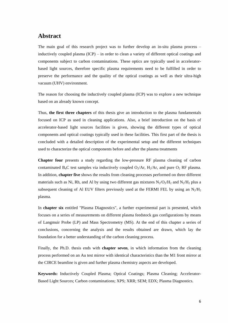
4.3.2 H2/Ar plasma cleaning ......................................................................................................... 62
X-ray Photoelectron Spectroscopy (XPS) analysis ........................................................................... 62
X-Ray Reflectometry (XRR) analysis ................................................................................................. 64
SEM results ....................................................................................................................................... 66
4.3.3 Pure O2 plasma cleaning ..................................................................................................... 67
X-ray Photoelectron Spectroscopy (XPS) analysis ........................................................................... 68
X-Ray Reflectometry (XRR) analysis ................................................................................................. 69
SEM results ....................................................................................................................................... 71
4.3.4 Considerations on a-C plasma cleaning mechanisms and cleaning speed .......................... 72
4.4 CHAPTER OVERVIEW .................................................................................................................. 74
5 TOWARDS CHEMICALLY NEUTRAL CARBON CLEANING PROCESSES: PLASMA
CLEANING OF NI, RH, AND AL REFLECTIVE COATINGS AND THIN AL EUV FILTERS FOR
FREE ELECTRON LASERS AND SYNCHROTRON BEAMLINE APPLICATIONS ...................... 77
5.1 OPENING ................................................................................................................................... 77
5.2 EXPERIMENTAL DESCRIPTION ..................................................................................................... 78
5.3 RESULTS AND DISCUSSION .......................................................................................................... 79
5.3.1 Nickel Spectra ...................................................................................................................... 79
5.3.2 Rhodium Spectra .................................................................................................................. 81
5.3.3 Aluminum Spectra ................................................................................................................ 83
5.3.4 Al EUV Filter Cleaning ....................................................................................................... 84
5.3.5 Considerations on a-C plasma cleaning mechanisms .......................................................... 85
5.3.6 Summary .............................................................................................................................. 89
6 PLASMA DIAGNOSTICS ........................................................................................................ 91
6.1 INTRODUCTION .......................................................................................................................... 91
6.2 EXPERIMENTAL SETUP ................................................................................................................ 91
6.3 RESULTS AND DISCUSSION .......................................................................................................... 93
6.3.1 Non-Maxwellian Characterization....................................................................................... 93
6.3.2 Maxwellian Characterization .............................................................................................. 94
6.3.3 Ion Energy Distributions (IEDs) .......................................................................................... 95
6.3.4 Cleaning Process and Reactions in the Ion Production ..................................................... 100
6.3.5 Additional Langmuir Probe Measurements ....................................................................... 104 6.3.5.1 Maxwellian characterization .................................................................................................... 104 6.3.5.2 Non-Maxwellian Characterization ........................................................................................... 106
6.4 SUMMARY ................................................................................................................................ 108
7 PLASMA CLEANING OF AU REFLECTIVE COATING ...................................................... 109
7.1 CLEANING THE TEST AU MIRROR (SESO) ................................................................................. 109
7.1.1 Experimental set-up ........................................................................................................... 109
7.1.2 Results and Discussion ...................................................................................................... 110
7.1.3 XPS .................................................................................................................................... 110
7.1.4 Interference microscopy ..................................................................................................... 112
7.1.5 Results from XRR measurements ....................................................................................... 114
7.1.6 Gas Analysis (RGA) ........................................................................................................... 115
7.1.7 Reflectance-based end-point detection setup .................................................................... 116

3
Acknowledgements
To thank is always complicated, just because there is constantly a new person showing up to
help me in every aspect of my life - even for simple things such as to make me laugh, which is
something which I appreciate the most. But in any case, I will try to name everyone who won
the right to be acknowledged in this humble work.
First of all I would like to thank my supervisor, Dr. Eric Pellegrin, for the patient guidance,
encouragement, and advice he has provided throughout my time during my Ph.D. I have been
lucky to have a supervisor who responded to my questions and queries so promptly. I thank to
the crew members of the “Vacuum Group at ALBA Synchrotron” Lluis and David, their
support was crucial to finish everything in due time, and to start everything in time. In
particular, I would also like to thank Jose Cotrino from the “Instituto de Ciencia de Materiales
de Sevilla” for the guidance and contributions he made in reference to Chapter 6 of this work. I
express also my gratitude to Francisco Yubero from the same Institute and Igors Sics from
ALBA staff. Their analysis and support made the construction of the prototype for reflectance
end point detection system shown in Chapter 7 possible. Special thanks to Muriel from the
“Soleil Synchrotron” and to Daniela Rogler from the “AXO Dresden GmbH” - although I don’t
know them personally, they definitely know my countless mails asking for them help in order to
measure the surface roughness of my samples.
I must express my gratitude to Kamile, my wife, for her continued support and encouragement.
I was continuously amazed by her patience and to my little boy - he motivates me all the time
just by his existence.
Completing this work would have been all the more difficult were it not for the support and
friendship provided by the other PhD roommates of our office. I am indebted to them for their
laughs - Isidro Crespo and Albert Castellví provided a much needed form of escape from my
research work - they also deserve thanks for helping me keeping things in perspective. Finally, I
would like to thank CELLS-ALBA and Vincent Carlino from ibss group, as without their
sponsorship I definitely could have done anything.

4
Bellaterra, Febrero 21 del 2018
Dr. Eric Pellegrin, miembro de la División de Experimentos en ALBA Sincrotrón, en calidad
de director de tesis y Dr. Javier Rodríguez Viejo, profesor de la Universitat Autònoma de
Barcelona, en calidad de tutor de tesis.
CERTIFICAN:
Que Harol Aníbal Moreno Fernández, Licenciado en Física, ha realizado bajo la dirección del
Dr. Eric Pellegrin el trabajo de tesis que lleva por título “Optimization of Remote Inductively
Coupled Plasma for the Cleaning of Different Optical Surfaces”. Dicho trabajo ha sido
desarrollado como parte del programa de doctorado de Física, financiado por la Generalitat de
Catalunya, Departament d’Empresa i Coneixement dentro del programa de Doctorados
Industriales (dossier no. 2014 DI 037). Este trabajo constituye su memoria de tesis doctoral,
para optar por el grado de Doctor en Física por la Universitat Autònoma de Barcelona.
Dr. Eric Pellegrin Dr. Javier Rodríguez Viejo
Harol Aníbal Moreno Fernández

5
6
Abstract
The main goal of this research project was to further develop an in-situ plasma process –
inductively coupled plasma (ICP) – in order to clean a variety of different optical coatings and
components subject to carbon contaminations. These optics are typically used in accelerator-
based light sources, therefore specific plasma requirements need to be fulfilled in order to
preserve the performance and the quality of the optical coatings as well as their ultra-high
vacuum (UHV) environment.
The reason for choosing the inductively coupled plasma (ICP) was to explore a new technique
based on an already known concept.
Thus, the first three chapters of this thesis give an introduction to the plasma fundamentals
focused on ICP as used in cleaning applications. Also, a brief introduction on the basis of
accelerator-based light sources facilities is given, showing the different types of optical
components and optical coatings typically used in these facilities. This first part of the thesis is
concluded with a detailed description of the experimental setup and the different techniques
used to characterize the optical components before and after the plasma treatments
Chapter four presents a study regarding the low-pressure RF plasma cleaning of carbon
contaminated B4C test samples via inductively coupled O2/Ar, H2/Ar, and pure O2 RF plasma.
In addition, chapter five shows the results from cleaning processes performed on three different
materials such as Ni, Rh, and Al by using two different gas mixtures N2/O2/H2 and N2/H2 plus a
subsequent cleaning of Al EUV filters previously used at the FERMI FEL by using an N2/H2
plasma.
In chapter six entitled "Plasma Diagnostics", a further experimental part is presented, which
focuses on a series of measurements on different plasma feedstock gas configurations by means
of Langmuir Probe (LP) and Mass Spectrometry (MS). At the end of this chapter a series of
conclusions, concerning the analysis and the results obtained are drawn, which lay the
foundation for a better understanding of the carbon cleaning process.
Finally, the Ph.D. thesis ends with chapter seven, in which information from the cleaning
process performed on an Au test mirror with identical characteristics than the M1 front mirror at
the CIRCE beamline is given and further plasma chemistry aspects are developed.
Keywords: Inductively Coupled Plasma; Optical Coatings; Plasma Cleaning; Accelerator-
Based Light Sources; Carbon contaminations; XPS; XRR; SEM; EDX; Plasma Diagnostics.

7

8

9
Introduction
Synchrotron radiation has become a powerful tool around the world. The increase of
synchrotron laboratories highlights the interest by commercial, educational and medical science
research for the analytical results possible with high-intensity light sources. New generations of
synchrotron sources with enhanced performance such as free electron lasers (FEL) open new
possibilities for fundamental and applied research, therefore, a pressing requirement is to
maintain the enhanced performance of these facilities, which includes the maintenance of the
pertinent reflective and transmission beamline optics.
However, these optics (reflective optics and transmission filters) are subject to carbon
contaminations buildup. These carbon contaminations - that are presumably produced via
cracking of CHx and CO2 residual gas molecules by photoelectrons emitted from the optical
components, can be rather complex depending on the specific case, due to the fact that they are
not only consisting of one single carbon allotrope but may also contain contributions from sp2
and sp3 hybridized carbon species. These contaminations are becoming a serious issue for the
operation of high-performance beam lines due to several reductions of photon flux, beam
coherence, creation of destructive interference and scattering losses. Previous publications [1-7]
have shown it may be possible to clean those carbon contaminations in a safe and efficient way
by using a different kind of plasmas as capacitively coupled plasma (CCP), Inductively coupled
plasma (ICP) and Microwave plasma getting different results depending on the gas mixture,
input power, frequencies and optical surface to be cleaned.
Plasmas are advantageous to clean carbon contaminations in a sense that they activate any
molecular gas by dissociation, thereby inducing physical sputtering, i.e., removing surface
atoms from a solid by means of impacting energetic particles, and/or chemical cleaning which -
unlike physical sputtering - consists of the formation of volatile molecules on the target surface
due to chemical reactions with incident chemically active species onto the surface.
Nevertheless, the non-equilibrium character of these plasmas and their rich plasma chemistry, in
particular their capability of producing large amount of radicals, ions, neutral stable species,
photons, electrons all reacting with each other, make them very complex and thus difficult to
understand. Therefore, they cannot be understood without the help of plasma diagnostics such
as, e.g., mass spectrometry and Langmuir probe (LP) analysis. Note that the importance of the
plasma diagnostics lies in the understanding of how the species produced in the plasma will
interact - not only with carbon contaminations, but also with the optical coatings themselves.

10
Among the most common optical coatings for synchrotron mirrors are Au, Ni, and Rh, used due
to their specific reflectivity characteristics. In the case of FELs, SiC is employed in the hard x-
ray range (2 to 20 keV) while B4C is preferably used in the soft x-ray photon energy range (0.5
to 2.5 keV photon energy). These are selected materials due to their mechanical hardness,
expected to be mostly resilient with respect to the extremely high brilliance of the impinging
FEL photon beam. This usage includes single coatings as well as multilayer mirror coatings
based on, for example, SiC/B4C multilayers.
For extreme ultraviolet radiation (EUV) and soft X-ray transmission filters, Al is the material of
choice, due to its peculiar mechanical properties, thermal conductance, and wide photon energy
bandpass while blocking visible light. Summarizing, the choice of the material depends on the
intended application and becomes an integral part of the complete mirror fabrication.
According to the foregoing, the main objective of this work is to establish an approach to clean
high-quality optical coatings in a safe, efficient, controlled and well-understood manner by
using plasma-based techniques. In this sense, it is essential to specify the kind of plasma and the
feedstock gas to be used in the cleaning process in order to avoid any detrimental effect on the
optical coating, and thus preserve the morphology and the chemical composition of the different
surfaces.
This work deals with different experimental approaches based on the low-pressure RF
downstream ICP plasma, where different test objects were cleaned using specific plasma
configurations. Among the cleaned test objects are: B4C-coated optics, Al EUV filters, Au, Al,
Ni, Rh materials and Au coated optics. The present study is based on the analysis of different
plasma configurations such as Ar, O2, O2/Ar, H2/Ar, N2/O2/H2 and N2/O2/H2 feedstock gases by
using a commercial plasma source, the model GV10x1 produced by ibss Group Inc. The first
part of this work consists of an overview with information on the plasma-related cleaning
applications and accelerator-based light sources. The second part gives a detailed experimental
description including the different techniques used not only to characterize the optical coating
and materials, but also on how to use the pertinent plasma diagnostics performed on some
plasma configurations in the context of this study. Subsequently, the results from the cleaning of
different optical coatings such as among others Al and B4C are shown. The thesis concludes
with the results from the in-situ plasma cleaning of a copy mirror with similar characteristics
than the mirror M1 from the CIRCE beamline. The carbon contamination was successfully
removed form that mirror optical surface, which indicates the importance of this application for
1 Further details on the GV10x source can be obtained from the pertinent patents (US Patents 7, 015, 415, B2; 6, 263,
831 B1; and 6, 112, 696).

11
the future process at ALBA as well as at other accelerator-based light source facilities. In this
specific plasma cleaning run, additional unexpected – but nevertheless scientifically relevant -
issues were also found and will thus be discussed.

12

13
Chapter 1
1 PLASMA CLEANING TECHNOLOGY FOR THE REMOVAL OF
CARBON CONTAMINATION
This chapter does not intend to give a complete introduction into plasma physics; its goal is
rather to give a short introduction into plasma cleaning technology as used for treating different
optical coatings at accelerator-based light sources such as synchrotrons and free electron lasers.
1.1 Plasma Fundamentals
Plasma exists in many forms in nature and has a widespread use in science and technology. It is
an ionized gas containing an appreciable number of free charges but being approximately
electrically neutral as a whole. In general, it is a mixture of three components: free electrons,
positive ions and neutral atoms (or molecules). Under special conditions, the plasma may also
contain negative ions, but here we will not discuss this case any further. Thus, in what follows
the term ‘ion’ always means ‘positive ion’ (or cation). We call an ionized gas ‘plasma’ if it is
electrically quasi-neutral and its properties are dominated by electric and/or magnetic forces. A
large number of free charges produces a high electrical conductivity and makes it possible to
easily establish electric currents which interact with applied magnetic fields and with those
generated by the current itself [8].
A huge percentage (> 99%) of matter in the universe apparently exists in the form of plasma: In
the stellar, interplanetary and interstellar medium, and the high altitude planetary atmospheres.
However, in dense and/or cold media in which life develops, the plasma state is rare due to the
tendency of free charges to recombine. In laboratories, energy must be supplied to a gas in order
to produce a plasma state and its prolonged maintenance, especially regarding the pre-
conditions in terms of plasma density and temperature required for plasma applications.
Thus, plasma is produced by a suitable form of low-pressure gas discharge. The resulting
plasma is usually characterized as ‘cold plasma’ which is the type of plasma we deal with in this
work. Cold plasma use to have an electron temperature of at least about 10,000ºK. Here, the fast
electrons in the high-energy tail of the electron energy distribution are energetic enough to
ionize atoms they collide with, often enough to overcome the recombination of ions and
electrons back into neutrals. Because of the large numbers, it is more convenient to express the
plasma temperature in electron-volts (eV). When T is such that the energy KT is equal to the

14
energy an electron gets when it falls through an electric potential of 1 Volt, then we say that the
temperature is 1 eV. Note that the average energy of a Maxwellian distribution is (3/2)KT,
therefore at 11,600 K, the plasma has an average energy of 1.5 eV per electron. Here, 1eV =
11,600K is the conversion factor between degree K and eV.
Due to the presence of free charge carriers, plasma react with respect to electromagnetic fields
conducting an electrical current and possessing a well-defined space potential. Positive ions
may be singly charged or multiply charged. For plasma containing only single charge ions, in
order to describe the ion population the ion density ni (where ni is the total number of particles
over the total volume), the electron density ne, and the neutral density na are required to
characterize the plasma.
The degree of ionization is defined with the particle densities nz not with the charge densities, so
there are two ways to define it:
𝜌𝑖 =∑ 𝑛𝑧𝑧
𝑛𝑎+∑ 𝑛𝑧𝑧 and 𝜌𝑖
′ =∑ 𝑛𝑧𝑧
𝑛𝑎, (1)
Where 𝜌𝑖′ is an approximation of 𝜌𝑖 for 𝜌𝑖 ≪ 1 which is usually the case. For ion sources,
values of 𝜌𝑖 are in the range of 10-5 to 10-3 [9]. Ionization mechanisms can differ depending on
the plasma-chemical system, according to Fridman (2008) p.14 [10], these mechanisms can be
divided up into 5 types:
1. Direct Ionization by direct electron impact
2. Stepwise ionization by electron impact
3. Ionization by collision of heavy particles
4. Photoionization
5. Surface Ionization (i.e., via electron emission)
The first process is the most important type of ionization in cold plasmas; in this case, an
electron with high kinetic energy promotes the ionization taking place via a collision between
the electron and a neutral atom or molecule. In the second type of ionization, an already excited
neutral species is ionized, while for the third case, the ionization takes place in a collision
between ion, molecules, and atoms. When a photon interacts with a neutral species, it generates
a photo-ionization. Finally, the fifth kind of ionization is produced via photoelectrons emitted
from the surface.
Due to the mechanisms of the ibss model GV10x plasma source used in the experiments
mentioned in this work, only the first four types of ionization will be taken into account.

15
1.2 Plasma for Cleaning Applications
In modern technology, plasma has many useful applications: They reach into a very large
amount of industries such as electronic devices, automotive, medical, electronics, textiles, and
material science. Since plasma technology is a relatively new emerging field, new plasma
applications are still being discovered and are a matter of intense research. Most useful plasma
applications revolve around the science of surface modifications. These plasma applications are
mainly related to plasma surface treatments such as, e.g., surface activation, plasma etching,
plasma coating and plasma cleaning. [Surface modifications will be largely achieved by means
of plasma surface treatments. Materials can have any size, from nano-sized components to
endless sheets in continuous production. A wide range of materials can be treated with plasma
surface technology, among others including glasses, metals, metalloids, rubbers, and polymers.
Plasma can modify surfaces in various ways, either as a preparation for subsequent surface
treatment steps or by the finishing layer being provided by the plasma surface treatment.
Because of the main interest of this work, only the plasma cleaning application will be
discussed.
In cleaning applications, the plasma breaks bonds and convers atoms or molecules deposited on
a surface into a volatile product. The plasma thus cleans the surface and prepares it for
subsequent modification or application steps. Therefore, residues from lubricants, grease,
biofilms, oxide layers or even silicones can be stripped off from the surface by a plasma
cleaning treatment. The work described in this thesis deals with the carbon cleaning
contamination on different the optical coatings and filters.
Different mechanisms take place when plasma acts to clean a surface and they depend strictly
on the plasma feedstock gas mixture, plasma power supply, pressure, and plasma process time;
the description of the pertinent mechanisms will be provided in the corresponding chapter
related to the different optical coatings that were subjected to plasma cleanings. Nonetheless, we
can already mention some initial approaches: Oxygen plasma reacts with carbon bonds
deposited on the optical surfaces, breaking the (hydro-)carbon bonds, and turning them into
volatile compounds like CO2 and CO. Hydrogen, conversely, is a good reducing agent, e.g., for
removing oxide films from metals. However, for the carbon removal a detailed explanation will
be given in the corresponding chapter. Nitrogen in a combination with hydrogen will form
ammonia which will reduce the carbon in a self-oxidizing process. These previous reactions can
be called chemical erosion or better “chemical cleaning”.

16
In contrast to the gases mentioned previously Ar is not chemically reactive, thus it does not
generate chemical cleaning but rather a physical one. In this sense, due to the relatively high Ar
atomic mass, the removal of atoms from a solid surface is due to the impact of energetic Ar
ions. This results from elastic energy transfer from incident particles to the target atoms.
Nevertheless, in the case of carbon cleaning, the physical sputtering coming from heavy Ar ions
is not the only mechanisms taking place, as there is also UV contribution. The different
mixtures O2/Ar and H2/Ar will be analyzed in Chapter 6.
1.3 Inductively Coupled Plasma
Inductively coupled plasma were used as thermal plasma on its first stages in the 1960s,
whereupon it was used in the early 1990s by IBM and LAM where by using a planar ICP setup
developed a low-pressure high-density plasma (HDP) for semiconductor processing. In
addition, ICP torches are commonly used in optical emission spectroscopy.
ICP can be generated by directing the energy of a radio frequency generator into a suitable gas.
Unlike capacitively coupled plasma (CCP), where a voltage is applied between two parallel
electrodes, the coupling in ICP is achieved by generating a magnetic field by passing a high-
frequency electric current through a cooled induction coil. This inductor generates a rapidly
oscillating magnetic field oriented along the axial direction of the coil. Thus, the energy is
supplied by electric currents inside the gas which are produced by electromagnetic induction.
The different geometries that can be used to produce ICP are shown in Figure 1. They consist of
cylindrical, planar and half-toroidal.
Figure 1 ICP geometries. Cylindrical A, planar B, half-toroidal C.
The ICP plasma is usually operated at lower pressures. Thus, at these lower pressures the RF
plasma is strongly non-equilibrium and cold (Fridman, 2008). Typically the frequency used in
industry corresponds to 27.12 or 13.56 MHz. The ICP tends to reach high currents as well as

17
elevated electrical conductivities and electron densities; this is because to be ignited, the
effective inductive coupling requires low plasma resistance. In this context, the coupling
between the coil and the plasma can be understood by imagining the coil as the primary multi-
turn windings, and the plasma representing the secondary single-turn winding of an AC voltage
transfomer.
Hereinafter, this thesis will focus on a cylindrical geometry (Figure 1a); the inductive coil
induces an electromagnetic field in the RF-ICP discharge gas volume. In this geometry, the
magnetic field is primary over the electric field, therefore to provide a reduced electric field E/p
(i.e., electric field over pressure) for the ionization it is required to work at low pressures. The
produced electron densities for this geometry oscillate in a range of 1011-1012 cm-3 more than 10
times the ones produced by a CCP.
Faraday’s induction law can be used to derive the electric field inside the discharge tube
surrounded by the coil, thus the electric field is:
𝐸(𝑟) = −𝑑𝜙𝐵
2𝜋𝑟𝑑𝑡, (2)
Where 𝜙𝐵 is the magnetic field crossing the loop of radius r parallel to the axis of the plasma
discharge tube. This magnetic field appears due to the flowing current through the coil hence the
plasma current can be expressed as j(r)=j0(r) eiwt if the plasma conductivity 𝜎 is assumed to be
constant and the pressure is low allowing the plasma to be collisionless. Then, by using the
Ampere’s law, it is possible to determine the current density along the plasma radius as
𝑗0 = 𝑗𝑏𝐼1 (𝑟
𝜚), (3)
Where 𝐼1 is the modified Bessel function and 𝜚 is the skin layer (Fridman, 2008) and
(Lieberman, 2005) [12].
According to Okumura [13], in an ICP the main adsorption energy mechanism is a Joule
heating. This heating results from the scattering of the electrons with other particles after being
accelerated by the E-field. Assuming the voltage drop per unit length of the electric field E and
taking the drift electron velocity equals leE being le the electron mobility, the joules heating
power P=(Va-Vb)I can be expressed as
𝑃 = 𝑒𝑛𝑒𝑙𝑒𝐸2, (4)

18
which is larger than the skin depth of the electromagnetic field, making it possible for electrons
under the skin layer to receive the energy from the externally applied electromagnetic field.
1.3.1 Break Down Magnetic Field in a Cylindrical ICP
The usual Paschen curves of a Townsend discharge are used to determine the spark breakdown
usually for the case of a CCP, where the curves will give the breakdown voltage as a function of
the pressure and the distance between capacitor plates. Paschen curves can be used in inductive
plasmas to show the breakdown magnetic field as a function of the pressure which depends on
the applied frequency and the diameter of the plasma volume where the plasma is ignited. By
using the approximate equation of Burm [14], it is possible to plot the breakdown magnetic field
for different feedstock gas configurations used with the GV10x plasma source as can be seen in
Figure 2, where R is the radius of the plasma tube.
𝐵𝑏𝑟𝑒𝑎𝑘𝑑𝑜𝑤𝑛 =𝐵𝑝
𝜔𝑅[ln(𝐴𝜋𝑅𝑝)−ln(ln(1+1
𝛽))]
, (5)
where β is a recombination parameter with values typically in the range of 0.01-0.1. Therefore,
in a discharge the expression ln (ln (1 +1
𝛽)) of the equation is almost constant, while A and B
are gas-dependent constants as shown in Table 1 and determined experimentally [10, 12].
Figure 2 Breakdown magnetic field of the GV10x for different feedstock gases.

19
Table 1 Experimental parameters A and B used in the equation 5
Gas A
(cm-1
torr-1
)
B
(Vcm-1
torr-1
)
Ar 11.5 176
O2 6.5 190
N2 11.8 325
H2 4.8 136
He 2.8 77
CH4 17 300
Air 15 365
For the commercial GV10x plasma source, the magnetic field can also be estimated for the
plasma source coil and because of the coil geometry, a simple approximation can be done. As
for the plasma coil, the number of turns is set to 8 with a separation of 5mm with respect to each
other (Figure 3); in this case, we can use the magnetic field for one spiral and add the rest of the
spirals making the center of the coil the reference point as follow
𝐵 ≈ ∑𝜇0𝐼𝑟2𝒖𝑧
2(𝑟2+(𝑧−𝑧𝑖)2)3/2
𝑁𝑖=1 , (6)
Figure 3 Basic scheme of the GV10x plasma tube for calculating the approximately generated magnetic field
If Z´=Zi the summation can be expressed as follow
𝐵 ≈ ∑𝜇0𝐼𝑟2𝒖𝑧
2
[
𝑟2
(cos(𝑡𝑎𝑛−1(𝑧𝑖−𝑧
𝑟)))
2
] 3/2
8𝑖=1 , (7)

20
Thus, the magnetic field for the GV10x plasma source operated at a RF power of 100W with a
current of ~8.5 A and coil radius of 15 mm is found to be approximately B=7.04x10⁻⁶T. Note
that this is just a rough approximation that could not be experimentally verified due to the fact
that one cannot insert a magnetic field probe into the plasma volume to measure the magnetic
breakdown field.
It also has to be noted that the value of the magnetic field is not stricly pressure-dependent for a
large pressure range - as in the case of the breakdown magnetic field of the standard Paschen
curve - but it gives an approximate value for the induced magnetic breakdown field within the
coil that can be contrasted with the systematics in the standard Paschen plots regarding the
different plasma feedstock gases used.

21
Chapter 2
2 ACCELERATORS-BASED LIGHT SOURCES AND OPTICS
This chapter gives a brief introduction into the basics of accelerator-based light sources facilities
and introduces the different types of optical components and optical coatings that can be found
in these research facilities
2.1 Synchrotron Light Sources
A synchrotron is a research facility based on a circular particle accelerator; it comes from the
cyclotron, in which the accelerated particle beam, generally electrons, travels around a circular
path. Usually, all charged particles undergoing an acceleration process do emit electromagnetic
radiation. The magnetic field that bends the particle beam into its closed path increases with
time during the accelerating process, thus being synchronized to the increasing kinetic energy of
the particles. Figure 4 shows a typical arrangement of the different accelerators in a synchrotron.
Figure 4 Typical Storage ring in a synchrotron. Electrons are accelerated in a linear accelerator (LINAC) passing to a
circular booster accelerator inside the storage ring. Subsequently, the electrons are injected into the storage ring
where bending magnets are installed to bend the electron trajectories. Quadrupole and sextupole magnets focus and
correct the electron beam.

22
In a synchrotron, the speed of the electrons is near the speed of light c, with energies in the
order of GeV, in this case, it is required consider the theory of relativity and use the Lorentz
transformation. Due to the space-time deformation resulting from the Lorentz transform, the
emitted radiation in a rest reference system goes throughout a cone oriented along the same
direction as the particle velocity vector. The foregoing is in contrast with the classic model,
where the particle radiation is emitted homogenously perpendicular to the acceleration direction
(Figure 5).
Figure 5 Agular radiation distribution emitted by a charged particle in a circular motion, where a is the centripetal
acceleration. For small velocities there is no emission in the direction parallel to the acceleration, classical case A. In
the relativistic case, for velocities near the speed of light, the distribution produces a cone tangential to the particle
trajectory.
Synchrotron radiation (SR) is a powerful tool in many science disciplines. This radiation is
often used in physics, chemistry, biology, medicine, and industrial applications. The radiation
produced in a synchrotron covers a continuous range between the infrared and the x-rays. This
radiation (photons) can interact in different ways with matter. The result of this interaction can
incur in changes of the incident light or/and changes in the affected matter. As a result, the
analysis of the response to this interaction can provide valuable information. Matter-radiation
interactions can be simplified in three groups: absorption, diffraction and reflection. Absorption
provides information related to the energy structure of the matter, thus, becoming the base for
spectroscopy. In this sense, the model of light adopted here is corpuscular.
Diffraction, at the contrary, is a manifestation of the wave nature of the light, providing
important information about the structure of the matter. Analyzing structures requires the use of

23
hard X-rays with energies in the order of keV. This is in order to, for instance, identify the
spatial arrangement of atoms within a crystal or the shape of complex molecules. Last but not
least, the reflection of the light is based on geometric optics and can be considered the base of
microscopy. In this case, the matter is modeled as a continuum, so, the solved structures have a
larger size than the light wavelength used to characterize them.
There are three types of magnetic structures used to produce synchrotron radiation: Bending
magnets, wigglers, and undulators [15]. Since the first observation of synchrotron radiation in
1945, storage rings have evolved through three generations. The first generation corresponds
with those built for energy physics research, where the radiation produced from the bending
magnets provided 105 times more continuous radiation than conventional laboratory sources.
The demand for SR in the 70s led Europe, Japan, and the United States of America to construct
the so-called second generation of SR sources that made up the first generation of accelerator-
based light sources dedicated to the application of synchrotron light.
Wiggler and undulators magnets are used in synchrotron facilities to offer a higher flux,
brightness, and spectral range than bending magnet sources. While these two are periodic
magnet structures, the spectrum produced is different. An undulator produces radiation with less
horizontal/vertical divergence with higher brilliance (measured in photons/(s mm2 mrad2 0.1%
bandwidth) than wigglers or bending magnets [16], it is a periodic magnet array that imposes a
periodic deflection onto a relativistic electron beam. The multipolar magnets are located in the
straight section of the storage ring. The third generation sources started operating in the 90’s
and the performance is based on the insertion of these undulators or wigglers reaching
brightness up to 1020. While in a second generation source, the resulting undulator beam
brightness is up to ~1016. The brightness is the concentration of radiation typically measured in
photons/(s mm2 0.1%bandwidth). Still an important goal to reach for a fourth generation light
source is to increase the photon beam brightness and brilliance by reducing the electron beam
emittance and thus the photon source size and divergence.
The important topic about synchrotron radiation lies not only in its wide spectral range (i.e.,
between infrared and x-rays) but also in its enhanced brightness (Figure 6), as this brightness
allows performing experiments in a relatively short time with, e.g., a high photon energy
resolution. It also means to be capable of observing process in real time such as phase
transitions or any chemical or structural change. As an example, this elevated brightness makes
it possible to obtain photon energy resolution values using beamline monochromators of 𝐸/
∆𝐸 ≈ 40000𝑒𝑉 (i.e., the photon energy bandwidth at 1000eV is about ∆𝐸 ≈ 0.025𝑒𝑉 [17]) at
still reasonable photon flux values.

24
In order to avoid collisions with residual gas molecules and other gaseous particles that can
deflect the electrons from their trajectory, it is required to keep the storage ring in Ultra High
Vacuum (UHV), corresponding to vacuum pressures in the order of 10-10 mbar. After it, the
radiation goes through a beamline front end and beamline optics to end up at the beamline
experimental end station, where a corresponding wavelength is selected by using the
corresponding beamline monochromator (grating or crystal). Also, attenuators filters and
mirrors are used to filter, deflect, and focus/collimate the photon beam, respectively.
Figure 6 Brilliance of x-ray sources: A historical graph showing the increase in terms of brilliance, left column.
Typical spectral brilliance curves of magnetic insertion devices used in third generation synchrotrons, center column.
Undulator and bending magnet schemes, right column. Images are taken from http://wiley-vch.e-
bookshelf.de/products/reading-epub/product-id/596420 (January 29, 2018)
2.2 Free Electron Lasers (FELs)
An extension of the undulator radiation source scheme - that has been so far extremely useful to
the synchrotron community - is known as free-electron laser (FEL). Using a FEL, it is possible
to study the time dynamics of atoms and molecules, at variance to synchrotron that can image
the nano-world in the picosecond time range, whereas the FEL offers few-femtosecond time
resolution. FELs produce extremely high brightness, transversely coherent radiation by inducing
a bunch-density modulation of the electron beam at optical wavelengths. This is achieved by the
interaction of a low emittance electron beam with a self-generated intense optical electric field
in the spatially periodic magnetic field of an undulator.

25
Interference effects from these interactions enhance the probability of each electron-emitting
radiation at wavelengths selected by a phase match between the electron energy and the
undulator period. As an FEL consist of one or several very long undulators, some imbalances
known as FEL instabilities do appear. They introduce correlations between the electrons and
allow the possibility of enhancing the x-ray brightness. An exponential growth of the emitted
radiation intensity at a particular wavelength is introduced by this instability. As Feldhaus et al.
[18] mentioned, the origin of these instabilities can come by the spontaneous undulator radiation
or an external seed field, usually called self-amplified spontaneous emission (SASE) and/or FEL
amplifier respectively.
The process involved in FELs consists of a relativistic electron beam moving through the
periodic magnetic field of an undulator. Due to the product of interactions between electron
oscillations and their produced undulator radiation, the above instability of the electron bunch is
created. These instabilities appear only when the charge density is sufficiently high while the
emittance and the energy spread is sufficiently low.
Classical theory is completely adequate to describe the physics of the free electron laser because
the photon energy of the FEL is orders of magnitude smaller than the electron energy bandwidth
involved. The electrons are deflected periodically by the magnetic field and can, therefore,
exchange energy with the superimposed radiation field E, therefore the mechanism of a FEL can
be derived from the equations of motion in the presence of a nearly constant radiation field in
the low-gain regime as:
𝑑𝐸𝑒
𝑑𝑡= �⃗�𝑒 �⃗⃗�, (8)
𝐸𝑒 is the electron energy, �⃗⃗� is the electric field vector, and �⃗�𝑒 is the electron velocity. However,
in the high-gain regime of the FEL, the simple theoretical approach indicated above is not
sufficient. It is now required to take into account the electrostatic forces between the electrons.
Therefore, one has to solve the equations of motion together with Maxwell’s equations in a self-
consistent way. This is possible by means of three- dimensional time-dependent numerical
simulation codes [18]. Then, the Lorentz equation will describe the forces on each electron
resulting from the combined undulator and radiation fields, and Maxwell’s wave equation
describes the electric field of the radiation as driven by the transverse electron current induced
by the fields. Consequently, according to Brian et al., equation [19] an electron’s rate of change
of energy may be written as
𝑑(𝛾𝑚𝑐2)
𝑑𝑡= −𝑒𝑬 ∙ 𝒗 ∝ �̅�𝑢[sin((𝑘1 + 𝑘𝑢)𝑧 − 𝑤1𝑡) + 𝑠𝑖𝑛((𝑘1 − 𝑘𝑢)𝑧 − 𝑤1𝑡)] (9)

26
which tells us how is the transversely oscillating electrons bunch at the resonant wavelength in a
fixed plane wave field of constant amplitude.
In addition to the former, the usually high reflectivity mirrors as used in synchrotron facilities
cannot be used for the FEL operation, because the intense collimated UV radiation would
destroy the metallic mirror surfaces.
2.3 Optics for Synchrotron and FEL Applications
The increasingly required light sources with ever higher brilliance and superior beam
performance put challenging demands on beamline optics. The extremely high heat load and
energy density of the photon beam requires sophisticated cooling and reflection geometries.
Lately, silicon became the material of choice for front-end optics for its high heat conductivity,
low linear thermal expansion coefficient, low beam degradation and accessible quality. Fused
silica is still frequently used for downstream optical elements where direct exposure to the
“white” photon beam is not an issue. Typical requirements are slope errors significantly below 1
arc second for aspheric elements and below 0.1 arc second for flats or spheres. Roughness down
to t sub-Angstrom level helps to keep every photon in the experiment. Coherency considerations
demand even harder specifications for surface height errors in the order of 1 nm (rms) over
optics as long as 1 m or even longer.
Among the criteria for selecting the material for synchrotron mirrors are the good optical
machinability, resistance to high heat loads, and UHV compatibility. Some of the materials that
fulfill these requirements are Fused silica, Zerodur, Si, GlidCop, Cu with NiP layer and Al with
NiP layer. While one of the most common optical coatings for synchrotron mirrors are - among
others - Rh, Ni, and Au, where these materials are chosen due to their good reflectivity
characteristics.
Aluminum is the most commonly used material for EUV and soft X-ray transmission filters due
to its peculiar mechanical properties, thermal conductance, and wide photon energy bandpass
while blocking the visible light.
In the case of optical coatings especially for FEL light sources, a SiC optical coating is
employed in the hard x-ray range (2 to 20 keV) while a B4C optical coating is preferably used in
the soft x-ray photon energy range (0.5 to 2.5 keV photon energy). These materials are
preferably used due to their mechanical hardness and are expected to be mostly resilient with
respect to the extremely high brilliance of the photon beam. This usage includes single coatings
as well as multilayer mirror coatings based on, e.g., SiC/B4C multilayers.

27
In most cases, the task of the beamline optics is to focus the source point together with a
diverging photon beam to a well-defined point or simply collimating a diverging beam. This is
commonly done by using non-planar mirror surface geometries such as, e.g., toroidal or
paraboloidal surface that are acting on the beam in both the sagittal and the meridional direction
(but include astigmatism as intrinsic aberration of these mirror shapes). Thus, if a better quality
of the image is required, the above mirror are to be replaced by surfaces with higher symmetry
such as spherical, cylindrical and plane elliptical may be used. Thus, the mirro bulk material,
surface geometry as well as the optical coating material strongly do depend on the intended
application and become an integral part of the beamline optical design and mirror fabrication
process. Figure 7 shows some examples regarding mirror surface geometries and materials.
Figure 7 Some geometrical configurations for synchrotron mirrors. On top, a toroidal mirror image courtesy of N.
Roman from ALBA synchrotron. In the center, a W/B4C mirror, image was taken from http://www.ntt-
at.com/product/multilayer/ (January 29, 2018). Bottom row, an ellipsoidal mirror, image was taken from
http://www.ntt-at.com/product/multilayer/. (January 29, 2018).and an Al parabolic mirror, image was taken from
http://mbdaps.com/precision-optical/parabolicmirrors.htm (January 29, 2018)
However, beamline optics operated in modern light source facilities such as synchrotrons and
FELs are subject to ubiquitous carbon contaminations, these contaminations are not only
consisting of one single carbon allotrope but may contain contributions from sp2 and sp3
hybridized carbon species represent a serious issue for the operation of high-performance beam

28
lines due to several reductions of photon flux, beam coherence, creation of destructive
interference and scattering losses.
The next chapter will introduce the experimental setup and characterization techniques that were
used to perform the in-situ and ex-situ plasma cleaning on different optical coatings.

29
Chapter 3
3 EXPERIMENTAL DESCRIPTION
This chapter starts giving an experimental setup description, including the different parameters
taken into account to perform the different plasma cleaning processes. In addition, different
techniques used to characterize the different optical coatings components before and after the
plasma treatments will be shown. This chapter then concludes with the plasma diagnostics
techniques as well as with the results that have been obtained from the characterization of the
plasma produced by the GV10x plasma source.
3.1 Cleaning Chamber configuration
The test chamber set-up for the plasma cleaning consists of a custom horizontal 55 Liter UHV
chamber of cylindrical shape made of 304L (i.e., EN 1.4301) stainless steel of 750mm length.
The distance from the plasma source end part to the center is about 680mm (see Figure 8). The
base pressure was kept at 3x10⁻⁷ mbar for which a 250l/s turbo molecular pump (TMP) unit was
installed at one chamber end.
At the opposite chamber end, a commercial RF ICP source (model GV10x Downstream Asher,
made by ibss Group, Inc., Burlingame, CA 940101, USA) was installed. The plasma source
operates with a RF of 13.56 MHz and a RF power up to 300W. The Downstream Asher
operation principle allows generating the plasma in a separate “remote plasma” volume
upstream the UHV chamber where the optical objects to be cleaned are located. With the plasma
source being localized outside the main chamber, the ionization of the different gases will only
take place within the upstream plasma source volume.
Amorphous carbon (a-C) coated quartz crystal was placed in one quartz crystal microbalance
(QCM) at a distance of 420 mm from the plasma source. Carbon cleaning rates were calculated
according to Gonzalez et al. [20] from the time evolution of the carbon thickness removed by
the plasma as measured by the QCM. The obtained a-C cleaning rate - as measured by a quartz
balance - depends on the gas mixture configuration, pressure, RF input power, and surface to be
cleaned. Typical cleaning times required for an O2/Ar or pure O2 plasma were in the range of
2.5 hours, whereas the corresponding cleaning times for an Ar/H2 plasma were in the range of
12.5 hours, starting from a-C coatings with the same thickness. In other configurations as
N2/O2/H2 and N2/H2 plasmas, the cleaning rate corresponds with 7.2 Å/min and 2.5 Å/min

30
respectively. This significant difference in terms of carbon cleaning rate is related to the oxygen
percentage in the former gas mixture. Table 2 shows some plasma configurations results, after
being optimized to achieve the best cleaning performance.
Table 2 Different plasma gas removal rates as measured with the QCM by using the GV10x plasma source at 100W
Plasma
driving Gas
Cleaning rate A/min Pressure
mbar
Gas Mixture % Comment
O2
8.4 5e-3 99.999 Used to clean B4C
and Au coatings
O2/Ar
10 &11.6 5e-3 83/17 & 95/5 Used to clean Au coatings
H2/Ar
2.4 & 1.7 2.7e-3 36/64 & 6/94 Used to clean oxidative
metallic surfaces
N2/O2/ H2 premix
8.0 4.8e-3 94/4/2 Test comparison gas
N2/H2 premix
3.5 5e-3 95/5 Used to clean oxidative
surfaces and EUV-filters
N2 1.7 3.3e-3 99.999 Test comparison gas
The plasma feedstock gas is supplied via the far end of the plasma tube; the exhaust side of the
plasma tube is connected to the cleaning chamber via a DN40CF flange (with a roughly 100
mm lateral offset with respect to the chamber cylinder axis). The exhaust end of the plasma tube
feeds into the UHV test chamber and the downstream plasma of chemically active species is
conducted through the chamber by the differential pressure from the TMP. This warrants for a
stable jet of chemically active species from the plasma discharge volume into the downstream
cleaning chamber, coherent with the Down Stream Asher operation principle of the GV10x
source. Such downstream plasma may safeguard the objects to be cleaned from the detrimental
kinetic effects via a direct exposure to the plasma itself (usually associated with direct DC and
RF plasmas).
Feedstock gas mixtures were supplied via flow meter gas supply system (model GF40/GF80
made by Brooks Instruments) with an automatic mixing rates control of the two gases involved.
This automatic system permits a precise chemistry control, allowing a constant gas mixing ratio
in the process. The experiments were done at a total chamber pressure in the range of 10-3 mbar;
this order of magnitude was selected according to the specific calibrations for each gas mixture
in which the highest carbon cleaning rate was obtained.

31
Figure 8 Schematical description of the plasma cleaning chamber (QCM: Quartz crystal monitor; RGA: Residual gas
analyzer; S.M.: Sample manipulator)
Optical emission spectra were measured using an Ocean Optics model USB2000+ optical
spectrometer via an optical vacuum feedthrough, installed at about 150mm downstream the
exhaust of the GV10x plasma source and perpendicular to the plasma source axis. Some specific
transitions taken into account for the plasma characterization from optical emission are shown
in Table 3.
Table 3 Optical emission parameters for some cleaning rates shown in table 2
Gas Mixture Optical Emission
Lines from Radicals
Emission Line
Ratio
O2/Ar Ar I 750.4 nm O* 95%
Ar 5%
H2/Ar H I (H*) 656.3 nm Ar 93%
H* 7%
O2 O I (O*) 777.2 nm --
N2 NIII 336.58

32
In addition, in order to detect ionic species generated by the plasma, a differentially pumped
residual gas analyzer (RGA) was installed at the remote end of the UHV chamber. For
additional experiments, a reflectance system was installed at the back end of the chamber, in
order to perform a direct measurement of the carbon thickness removal by means of changes in
the mirror reflectance. A more detailed explanation on the latter system will be provided in
chapter 7.
3.2 Sample Preparation
For the amorphous carbon (a-C) layers deposition– i.e., for simulating a photon-beam induced
carbon contamination - onto the different optical coating test samples, a commercial e-beam
deposition chamber has been used to deposit between 50-180 nm of amorphous carbon (i.e., a
mixture of sp2 and sp3 carbon) from graphitic carbon targets (Goodfellow carbon target model C
009600) within about 200 seconds deposition time. This a-C thickness usually provides a
sufficiently long cleaning time for the analysis and optimization of the plasma cleaning process.
In addition, significantly less corrugated a-C layers were prepared by using a commercial
coating system (model Leica EM ACE600) at the electron microscopy division of the Institut
Catala de Nanociencia i Nanotecnologia (ICN2), with coating thicknesses in the range of 50-80
nm. This system is typically used to prepare precise coatings of samples for subsequent
examination with an electron microscope. The system has an automated stage rotation
integrated for achieving a better homogeneity/unformity of the carbon layer. The carbon
deposition is achieved by carbon thread evaporation. As this carbon tends to be quite
homogenous and reflective, it was used for later reflectance measurements and subsequent
plasma cleaning processes.
A more detailed explanation and characterization of the deposited carbon layers will be
provided in the Raman spectroscopy subsection of this chapter.
3.3 Characterization Techniques
Different characterization techniques were used to conduct a specific analysis either on the
optical coating surfaces resulting from the plasma chemistry or on the carbon deposited on top
the optical coatings.

33
3.3.1 Mass Spectrometry
Contemporary mass spectrometry is a micro-analytical technique that is used to detect gas-phase
ions generated from a gaseous, liquid, or solid sample to determine quantitatively its
composition and to reveal the structural information of detected compounds. It is a diagnostic
technique with unequaled sensitivity, detection limits, and speed. It plays a dominant role in
biological sciences providing quantitative and structural information at a high throughput. It is
also applied in fields such as pollution and food control, forensic science atomic physics,
reaction physics and kinetics, inorganic chemical analysis among others. The complete process
involves the conversion of the sample into gaseous ions, with or without fragmentation, which
is then characterized by their mass to charge ratios (m/z) and relative abundances.
This technique basically studies the effect of ionizing energy on molecules. It depends upon
chemical reactions in the gas phase in which sample molecules are consumed during the
formation of ionic and neutral species. A mass spectrometer generates multiple ions from the
sample under investigation; it then separates them according to their specific mass to charge
ratio (m/z) and then records the relative abundance of each ion type.
The first step in the mass spectrometry analysis of compounds is to produce ions in gas phase
from the compound, basically by electron ionization. This molecular ion undergoes
fragmentation. Each primary produced ion derived from the molecular ion, in turn, undergoes
fragmentation, and so on. The ions are separated in the mass spectrometer according to their
mass to charge ratio and are detected in proportion to their abundance. A mass spectrum of the
molecule is thus produced. It displays the result in the form of a plot of ion abundance versus
m/z. Ions provide information concerning the nature and the structure of their precursor
molecule. In the spectrum of a pure compound, the molecular ion, if present, appears at the
highest value of m/z (followed by ions containing heavier isotopes) and gives the molecular
mass of the compound.
The technique started to be developed in the 1900s. The first instruments capable to measure the
mass spectra date from 1912. Figure 9A shows the illustration of the mass spectrometer (MS)
consisting of major components as:
a. Ion Source, for producing gaseous ions from the substance being studied.
b. Energy analyzer and m/z analyzer, for resolving the ions into their characteristics mass
components according to their mass-to-charge ratio (the energy analyzer is only
required in cases where it is required to run an energy analysis, therefore this
component is not placed in all mass spectrometers).

34
c. Detector System, which allows ions detection and recording the relative abundance of
each of the resolved ionic species.
In line with our interest in plasma diagnosis, this section will focus on quadrupole mass
spectrometry typically used to characterize reactive plasmas.
One important requirement before starting the analysis is to maintain some vacuum
requirements; therefore the operative pressure should be lower 10-4 mbar to assure the ion
trajectory in the MS is lower than the ion mean free path. Although, while working with
plasmas it will be mandatory to make use of a differentially pumped vacuum chamber to install
the MS and measure through a sampling orifice, in order to operate the secondary electron
multiplier (SEM) detector which will require pressure lower than 10-6 mbar.
Measuring ions is achieved by focusing them with electrostatic lenses (ion optics) into the MS.
To analyze plasma with a MS, lenses are installed in front the ionizer; therefore the detection of
ions or neutrals is possible by using the same device. Different methods of ionization can be
used as for example electron impact ionization (EII), dissociative electron attachment (DEA),
chemical ionization, thermal photoionization or photoionization. When working with low-
temperature plasmas is commonly used the EII, this technique is -besides photon and ion impact
ionization- the main ionization mechanism in laboratory plasmas. Thus we are going to restrict
the forthcoming analysis to this method. In EII, the gas is bombarded by energetic electrons
generated from a heated filament in the ion source. This interaction generates a radical cation
(M+•
) and two electrons [21]
𝑀 + 𝑒− → 𝑀+∙ + 2𝑒− (10)
Where 𝑀+∙is the molecular ion, and its m/z corresponds to the molecular mass of the introduced
gas. The primary hindrance of this technique is that it can cause extensive molecule
fragmentation which reduces the detection sensitivity. This can be solved by choosing energies
for electrons near to the ionization potential of the main species within the plasma.
However, it should be taken into account that by using hot filaments, this can lead to the
generation of additional species near the ionizer, for example in the case of hydrogen plasma,
CO or CH4 can be generated and the pump of H2 entering into the MS tends to be deficient. The
former will provide with a hydrogen background pressure in the MS, according to Benedikt et
al., [21] this internal generation of hydrogen may be larger than the hydrogen coming from the
plasma, making the detection of hydrogen generated in the plasma impossible.

35
Figure 9 A: QMS scheme, B: Schematic representation of electrostatic energy analyzer (ESA).
To perform the ion selection with respect to their energy, energy analyzers with different
designs named as Bessel box type, sector field electrostatic energy analyzers (ESAs) and Wien
filter are used. As the quadrupole mass spectrometer that was used in this work to analyze the
plasma corresponds with ESAs, let’s focus on the description of this analyzer.
The concept of ESAs is based on the use of electrostatic field produced between two charged
electrodes. These electrodes can have parallel plates, cylindrical, spherical or toroidal
configurations, where the most common are cylindrical configurations with a sector angle of 45º
or 90º (Figure 9B). To guide ions entering the ESA with and energy Eion on a circular trajectory
along the optical axes, an electric field E=V/d is selected where d is the distance between the
plates. Then, there should be a balance between the centripetal force generated by the electric
field and the centrifugal force, this balance can be written as:
𝑧𝑒𝐸 =𝑚𝑣0
2
𝑟𝑒=
2𝐸𝑖𝑜𝑛
𝑟𝑒→ 𝐸 =
2𝐸𝑖𝑜𝑛
𝑧𝑒𝑟𝑒, … (11)
where z is the charge state of the ion. Although for cylindrical configurations, it is required a
modification in the expression, and according to Perrin [22] the following relation between the
energy of the particle Eion and applied voltage (V0) should be used

36
𝐸𝑖𝑜𝑛 =𝑧𝑒𝑉0
2ln (𝑟2/𝑟1). (12)
Ions entering the ESA are deflected according to their kinetic energy independently of their m/z
ratio.
The kinetic energy resolved by the MS measurement of ion fluxes is named Ion Energy
Distribution Function (IEDF); it provides important information about the plasma process. The
shape of the IEDF is governed by the frequency and the collisions. The frequency of the applied
bias could be lower than the plasma ion frequency. By doing this, the ion energy directly
reflects the voltage applied to the substrate, this is possible because the ion transition time
through the sheath is short. At the contrary, if the frequency is of the order of the ion plasma
frequency or higher, during the ion transition through the sheath, the ions will see a modulated
potential that will cause an average energy after the impact.
In the case of the collisions, the charge exchange collisions in the sheath generate new ions
which will reach the surface at a lower energy in contrast with the sheath potential. Therefore,
depending on the sheath frequency - low or RF - may be generated two different IEDFs. In low-
frequency sheaths as DC or pulsed DC (e.g., for example magnetron discharges), the IEDFs are
characterized by two high-energy tails that can be compared by a shifted Maxwellian
distribution [21]. The magnets located behind the target enhance the ionization process even at
lower pressures. These IEDF can be explained by charge exchange and/or elastic process in the
plasma sheath.
Conversely, in high-frequency sheaths typically RF plasmas with a frequency of 13.56MHz or
higher that are those generated by CCP or ICP, the sheath potential is directly affected by the
time modulation of the plasma potential. In this case, the IEDF is a function of the ion transit
across the sheath. Two distinct features are distinguishable in IEDFs for high sheaths
frequencies. In the first case, one single peak can appear, it corresponds to an ions transit time
longer than the RF period, for example, Ar+. In the second case, a double peak structure show-
up, this is related to ions transit time shorter than the RF period as in the case of H+, some
examples of these two characteristic IEDFs behaviors for the high-frequency sheath in and ICP
can be observed in Figure 10.

37
Figure 10 Two distinct features for high-frequency sheaths in H2/A2 plasma produced by the GV10x at 100W. Red
line shows the IEDF behavior for ion transit times longer than the RF period. The black line shows the IEDF for ion
transit time shorter than the RF period.
To perform mass analysis, a quadrupole mass spectrometer is usually chosen. This is based on
its low cost, lightweight, simple operation among other characteristics. Unfortunately, its
resolution is low (~0.3 m/z), in addition, is difficult to measure quantitatively very light atoms
such as atomic hydrogen.
The quadrupole consists of four parallel metal rods. A pair rod opposing each other is connected
together electrically, and a RF voltage with a DC offset voltage is applied between one pair of
rods. Ions will travel down the quadrupole between the rods as can be seen in Figure 11. Only
ions of a certain mass to charge ratio will reach the detector for a given value of voltages; other
ions have unstable trajectories and will collide with the rods.
This allows the selection of a specific ion with a particular m/z. To operate in a continuous
range of m/z values, the applied voltage will be varying continuously. After the ions have been
separated -based on their m/z ratio- they are transformed into a measurable signal. This
detection is carried out by an ion detector and in the case of QMS, the most typical detector is
the called SEM which is made by continuous or discreet dynodes. For a complete description of
QMS see references [21, 22].

38
Figure 11 Electrical connection of a cylindrical QMS.
3.3.1.1 System description
A mass energy analyzer model “HAL EQP/EQS” from HIDEN ANALYTICAL LTD was used to
carry out the plasma characterization shown in chapter 6. This Analyzer is a high-transmission
45º sector field ion energy analyzer and quadrupole mass spectrometer; it is designed as a
diagnostic tool for plasma or Secondary Ion Mass Spectrometer (SIMS) analysis. Mass spectra,
energy spectra, and appearance potential profiles will be acquired, allowing detailed analysis of
positive ions, negative ions, radicals, and neutrals. The Electrostatic Quadrupole Plasma (EQP)
Analyzer considers the energy and mass-to-charge ratio distributions of ions, neutrals or radicals
generated in the plasma source. It can be used to study transients and afterglows with fast data
acquisition; the system is also suitable for ion flux analysis from ion sources and drift tubes.
The Electrostatic Quadrupole SIMS (EQS) Analyzer, analyses the energy and mass-to-charge
ratio distributions of secondary ions or neutrals generated by interaction with a surface under
high vacuum. The interaction may, for example, be ion, or another particle, bombardment of the
surface, or the ionizing action of a laser on the surface. Neutrals or radicals in the gaseous
chamber environment can also be analyzed.
Figure 12 shows the typical standard EQP system Analyzer. EQP and EQS analyzer are
identical with the exception of the front of the Probe, where the method of pumping the Probe
and the components forming the ion extraction system differ. The EQP Analyzer Probe samples
via a small orifice (50 µm to 300 µm in diameter) being pumped differentially, in our
experiments it was used the 50 µm diameter orifice. The EQS Analyzer Probe samples via a
large orifice and is pumped by the host system pumps. The EQP Probe requires a 60 L/s
pumping unit; double or triple pumping stages are available for high-pressure applications. In

39
both types of Analyzer, analysis of neutrals and radicals is achieved by the use of a twin-
filament, fully-adjustable electron-impact ion source. In all cases, the ions are focused into an
electrostatic field energy filter, which provides energy analysis; this is followed by a triple-
section quadrupole mass filter for mass-to-charge ratio analysis.
Figure 12 Typical standard EQP system. Image taken from EQP/EQS Analyzer operator´s Manual of Hiden
Analytical Limited. p. 8. (February 2, 2018)
The EQP is used where the external ion source is plasma, and the EQS where the source is, for
example, a bombarded surface or laser-induced ionization at high vacuum. The probes for these
analyzers are comprised of 5 sections: extractor, RGA source, energy analyzer, quadrupole mass
filter, and detector.
3.3.2 Langmuir Probe
A Langmuir probe is a plasma diagnosis device used to determine the electron temperature,
electron density, and electric plasma potential. A Langmuir probe consists of a bare wire or
metal disk, which is inserted into a plasma and biased electrically with respect to a reference
electrode to collect electron and/or positive ion currents. Plasma physicists use Langmuir probes
in low-temperature plasmas approximately a few electron volts to measure the plasma density,
electron temperature, and plasma potential.
Originally, the probes were called “sounding electrodes” used initially at the end of the nineties
in an attempt to measure the voltage distribution in gas discharges. The early users of probes
instinctively assumed that the potential of the plasma at the location of the probe, known as the
plasma potential (VP) or space potential could be determined by measuring the potential on the

40
probe relative to one of the electrodes. However, this procedure determined the floating
potential (Vf) of the probe which is generally not the same as the VP. By definition, a probe that
is electrically floating collects no net current from the plasma, and thus its potential rises and
falls to whatever potential is necessary to maintain zero net currents.
In common plasmas, the electrons, have significantly higher thermal speeds than the positive
ions due to the mass difference, even if there is a thermal equilibrium. Often, the electrons have
a higher temperature than the positive ions. Although in a plasma, considerations as the
electrical neutrality, ion, and electron density neutrality, a floating probe will tend initially to
draw a higher electron current inasmuch as the electrons reach the probe faster than the more
massive ions. Because the net current of the floating probe must be zero, the probe floats to a
negative potential relative to the plasma so that further collection of electrons is retarded and the
ion collection is enhanced. Thus, the floating potential is less than the plasma potential.
The plasma potential is the potential of the plasma with respect to the walls of the device at a
given location in the plasma. VP is generally a few volts positive with respect to the walls, again
because the faster electrons tend to escape to the walls firstly, leaving the plasma with a slight
excess of positive space charge. However, the plasma bulk is quasi-neutral, and the potential
difference between the bulk of the plasma and the wall is concentrated in a thin layer “sheath”
near the wall.
The gradient of the plasma potential determines the electric field that is responsible for
energizing the electrons that maintain the discharge through ionization. Although physicists
knew that Vf and VP were not the same, they thought that the difference was probably small, and
in any case, they had no way of either estimating the difference or of measuring the actual
plasma potential. Irving Langmuir and Harold Mott-Smith of the General Electric Research
Laboratory in 1920 were the first to provide a quantitative understanding of the difference
between Vf and VP [23]
Langmuir’s method consists of obtaining the current-voltage I-V characteristic of the probe as
the applied bias voltage (VB), swiping from a negative to a positive potential. The difficulty to
understand the characteristics I-V curves of the LP comes from the fact that the electrons and
ions are not monoenergetic and often have very different temperatures. As a result, the probe
sometimes collects only ion current, sometimes only electron current, and sometimes both. It is
easier to understand and analyze the full I-V characteristic if the ion and electron current
contributions are separated.

41
The typically I-V trend is usually displayed upside down so that electron current into the probe
is in the positive y-direction as can be seen in Figure 13. The point at which the curve crosses
the x-axis is called the floating potential Vf. To the left of this, the probe draws ion current and
the curve soon flattens out to a more or less constant value called the ion saturation current (Isat).
To the right of Vf, the electron current is drawn, and the I-V curve goes into an exponential part,
or transition region, as the Coulomb barrier is lowered to allow slower electrons in the
Maxwellian distribution to penetrate it. At the space potential, the curve takes a sharp turn,
called the knee, and saturates at the electron saturation current Ies. Actual I-V curves in RF or
magnetized plasmas usually have an indistinct knee.
Figure 13 I-V curve from the ICP GV10x in and AR plasma discharge
When the bias voltage, on the probe, is sufficiently negative with respect to the plasma
potential, the probe collects the ion saturation current. Positive ions continue to be collected by
the probe until the bias voltage reaches VP, at this point ions begin to be repelled by the probe.
For VB>>VP, all positive ions are repelled, and the ion current to the probe vanishes, Ii=0. For a
Maxwellian ion distribution at the temperature Ti, the dependence of the ion current Ii (VB) on VB
is given by
𝐼𝑖(𝑉𝐵) = 𝐼𝑖𝑠𝑒𝑥𝑝[𝑒(𝑉𝑝 − 𝑉𝐵)/𝐾𝑇𝑖] … (13)
Taking the ion thermal speed as 𝑣𝑖 = √8𝑘𝑇𝑖
𝜋𝑚𝑖, when Te~Ti the ion saturation current is given by

42
𝐼𝑖𝑠 =1
4𝑒𝑛𝑖𝑣𝑖𝐴, (14)
for 𝑛𝑖 as the ion density and 𝐴 as the probe collecting area. However if, Te>>Ti , to calculate the
ion saturation current it will be required the Bohm ion current according with Merlino [23].
Therefore
𝐼𝑖𝑠 = 0.5𝑒𝑛𝑖√𝑘𝑇𝑖
𝑚𝑖𝐴 (15)
The electron saturation current is given by
𝐼𝑒𝑠 =1
4𝑒𝑛𝑒𝑣𝑒𝐴 = 𝑒𝑛𝑒√
𝑘𝑇𝑒
2𝜋𝑚𝐴 (16)
For a cylindrical probe as the negative bias is increase to draw Ii the sheath expands, and Ii does
not saturate. Different theories can be used to characterize the plasma as for example the orbital-
motion- limited (OML) theory of Langmuir which assumes large sheaths such that 𝜉 ≡𝑅𝑝
𝜆𝐷≫
1 where 𝑅𝑝 is the probe radius and 𝜆𝐷the Debye length. Another theory is the Allen- Bod-
Reynolds (ABR), in this theory ions are all drawn radially into the probe. Originally, the ABR
theory was only for spherical probes, but it was later extended to cylindrical probes by Chen
[24, 25]. The Bernstein-Rabinowitz-Laframboise (BRL) theory is the first theory which account
for sheath formation as for orbital motions. In ABR, all ions strike the probe, so the flux at any
radius depends on the conditions at infinity regardless of the probe radius. In BRL theory,
however, the probe radius must be specified beforehand, since those ions that orbit the probe
will contribute twice to the ion density at any given radius r, while those that are collected
contribute only once [25].
The floating potential is defined by Ii=Ie, where Ie is given by equation 13 and16. If the
electrons are Maxwellian, Ii can be calculated from one of the theories presented in the previous
paragraph. The Bohm current can be used from equation 15, where the current is caused by the
electric field in the pre-sheath which accelerates ions to a velocity of 𝑣𝑖 = √𝑘𝑇𝑖
𝑚𝑖, the minimum to
form a sheath. Therefore the plasma potential can be determined by
𝑉𝑓 = 𝑉𝑠 −𝐾𝑇𝑒
2𝑒𝑙𝑛 (
2𝑀
𝜋𝑚), (17)
Where Vf-Vs is ~3.2Tev for hydrogen and -5.4Tev for argon in planar geometries and between -4
and -5TeV in cylindrical geometries.

43
3.3.2.1 System Description
Since the probe is immersed in a harsh environment, special techniques are used to protect it
from the plasma and vice versa, and to ensure that the circuitry gives the correct I-V values. The
probe tip is made of a high-temperature material, usually tungsten rod or wire 0.1-1 mm in
diameter. The rod is threaded into a thin ceramic tube, usually alumina, to insulate it from the
plasma except for a short length of the exposed tip, about 2-10 mm long. These materials can be
exposed to low-temperature laboratory plasmas without melting or excessive sputtering.
To avoid disturbing the plasma, the ceramic tube should be as thin as possible, preferably <1
mm in diameter but usually several times this. The probe tip should extend out of the end of the
tube without touching it so that it would not be in electrical contact with any conducting coating
that may deposit onto the insulator.
For our measurements a LP (model-Plasma Consult GmbH, L2P system) is used to measure the
characteristic plasma parameters as electron temperature, ion density, plasma potential and
floating potential to each gas mixture used.
3.3.3 Raman Spectroscopy
Raman spectroscopy is a spectroscopic technique based on inelastic scattering of
monochromatic light, usually from a laser source. Inelastic scattering means that the frequency
of photons in monochromatic light changes upon interaction with a sample. Photons of the laser
light are absorbed by the sample and then re-emitted. The frequency of the re-emitted photons is
shifted up or down in comparison with original monochromatic frequency, this phenomenon is
called the Raman Effect. This shift provides information about vibrational, rotational and other
low-frequency transitions in molecules. Raman spectroscopy can be used to study solid, liquid
and gaseous samples.
The Raman effect is based on molecular deformations in an electric field E determined by
molecular polarizability 𝛼. The laser beam can be considered as an oscillating electromagnetic
wave with electrical vector E. Upon interaction with the sample it induces electric dipole
moment 𝑃 = 𝛼𝐸 which deforms molecules. Because of periodical deformation, molecules start
vibrating with characteristic frequency 𝜈𝑚. The amplitude of vibration is called a nuclear
displacement. In other words, monochromatic laser light with frequency 𝜈0 excites molecules

44
and transforms them into oscillating dipoles. Such oscillating dipoles emit light of three
different frequencies name as: Rayleigh scattering, Stokes frequency and anti-Stokes frequency.
The Rayleigh scattering appears when a molecule with no Raman-active modes absorbs a
photon with the frequency 𝜈0. The excited molecule returns back to the same basic vibrational
state and emits light with the same frequency 𝜈0 as the excitation source. In the case of Stokes
frequency, a photon with frequency 𝜈0 is absorbed by Raman-active molecule which at the time
of interaction is in the basic vibrational state. Part of the photon’s energy is transferred to the
Raman-active mode with frequency 𝜈𝑚 and the resulting frequency of scattered light is reduced
to 𝜈0 − 𝜈𝑚. Finally the anti-Stokes frequency occurs when a photon with frequency 𝜈0 is
absorbed by a Raman-active molecule, which, at the time of interaction, is already in the excited
vibrational state. Excessive energy of excited Raman active mode is released, molecule returns
to the basic vibrational state and the resulting frequency of scattered light goes up to 𝜈0 + 𝜈𝑚.
Figure 14 Raman spectra from different carbon contaminations. Red solid line: Carbon footprint on EUV Al filter
foil upstream side; Black solid line: a-C thin film from e-beam carbon deposition; Blue solid line: Carbon footprint
on EUV Al filter foil downstream side; green solid line: Carbon footprint an Au-coated from SRC soft X-ray
beamline.
Raman spectroscopy was used to characterize the different carbon contaminations on various
samples in order to establish a comparison between the carbon cleaning characteristic of the
carbon deposited on self-sustained ultrathin Al filters (Luxel Corporation, Friday Harbor, WA,
USA) with 100 nm thickness contaminated by the filter exposure to the FEL photon beam

45
operation at the FERMI FEL1, a carbon contamination from a gold-coated mirror used at a soft-
ray bending magnet beamline at the former Synchrotron Radiation Center (SRC) and a set of
Ni, Rh, Al, Si test samples deposited with micrometric thickness amorphous carbon for
simulating a photon-beam induced carbon contamination. Figure 14 shows the Raman spectra
for these three different contaminations. The most intense contamination corresponds to the
upstream side of the EUV filter, showing two characteristic carbon-related peaks denoted as D
(1378cm-1) and G (1542cm-1).
Although these peaks can be seen, still the carbon contained is related to amorphous carbon (a-
C) with little graphitic ordering, the same counts for the contamination from the back side and
the SRC carbon contamination. Note that in graphite the G mode is at 1581 cm-1 involving the
in-plain bond-stretching motion of C sp2 atom pairs, while the D peak lies around 1355cm-1 and
is known as a defect mode. This mode is forbidden in perfect graphite and only gets active in
presence of disorder [26]. In this context, it is possible to deduce that the carbon contaminations
on the Al filter foils do not show a purely graphitic behavior, as they rather consist of a mixture
of sp2 and sp3 hybridized carbon consisting of broad and smooth Raman spectral features.
Hence, the broadening Raman bands and the high intensity of the D peak relative to the G peak
indicate a low graphitic content in the carbon contamination footprint [27].
3.3.3.1 System description
The micro-Raman setup used on the different carbon characterizations consists mainly of a
high-throughput, high-resolution Jobin-Yvon LabRam HR800 grating spectrometer combined
with a confocal microscope for optical studies using diverse experimental techniques like
Raman scattering and photoluminescence (PL)
a. Spectral range: Near-infrared (1.7 µm) up to 400 nm.
b. Spatial resolution: 1 µm
c. Optical measurements at low Temperature (10 to 300 K) is possible using a gas-flow
cryostat from CryoVac that fits under the microscope of the micro-Raman spectrometer.
The Raman set up is based on a filter stage with a dynamic holder for interchanging several
notch filters for different laser wavelengths, 488 and 514.5 nm from an air-cooled Ar-ion laser,
632.5 nm from He-Ne laser and 785 nm from a solid-state laser. The microscope is further
equipped with a remote-controlled x-y stage allowing to perform line scans automatically. The
characteristics of this spectrometer are, on the one hand, its high spectral resolution due to a
large focal length of 800 mm and three gratings for the infra-red and visible range (1800, 900
and 650 lines/mm) and, additionally, its high sensitivity due to low-noise, high quantum

46
efficiency silicon CCD detector for the visible spectral range and a single-channel InGaAs
photodiode for the near infrared.
3.3.4 X-Ray photoemission spectroscopy
X-ray photoelectron spectroscopy (XPS) was developed in the mid-1960s by Kai Siegbahn at
the Uppsala University, Sweden. XPS is also known as electron spectroscopy for chemical
analysis (ESCA) as it was baptized at the beginning [28]. This technique allows analyzing the
surface chemistry of a material. XPS can measure the elemental composition, empirical
formula, chemical state and electronic state of the elements within a material. XPS is in
principle, based on a particularly simple process. Electrons within a sample absorb photons of a
particular energy and then emerge from the solid. The kinetic energy analysis of electrons
emitted from the top 1-10 nm of the surface yields information on the electronic states of atoms
in the surface region.
A photoelectron spectrum is recorded by counting ejected electrons over a range of electron
kinetic energies. Peaks appear in the spectrum from atoms emitting electrons of a particular
characteristic energy. XPS is prominent in its popularity, versatility, and utility compared with
many other techniques because it enables the identification and quantification of all surface
elements (except hydrogen).
The sample is irradiated with monoenergetic soft x-rays, the usually x-ray sources are Mg Kα
(1253.0eV), Al kα (1486.6eV) or monochromatic Al Kα (1486.7eV). These photons have a
penetration depth of 1-10 micrometers. The emitted electrons from the surface after the
interaction will have energies given by
KE = hν − BE − ϕs, (18)
where hν is the photon energy, BE is the binding energy of the atomic orbital from which the
electron is emitted and ϕs is the work function dependent on the spectrometer and the material.
This equation basically is a conservation energy equation; the work function is an adjustable
instrumental correction factor that accounts for the few eV of kinetic energy given up by the
photoelectron as it becomes absorbed by the instrument's detector, it tends to be constant. The
photoemission process involved in XPS can be seen in Figure 15A.
The Fermi level corresponds to zero binding energy and the depth beneath the Fermi level
indicates the relative energy of the ion remaining after electron emission or the electron binding
energy. Because each element has a unique set of binding energies, XPS is used to identify and
determine the concentration of every element in the surface and by analyzing the chemical shifts

47
which correspond with the variation in the elemental binding energies, it can be possible to
identify the chemical state of the materials being analyzed.
Figure 15 Photoemission process involved in XPS. A. an incoming photon causes the emission of a photoelectron. B.
the relaxation process resulting in the emission of a KL23L23 electron (Auger electron).
In addition to photoelectrons emitted, Auger electrons are emitted due to the relaxation of the
excited ions remaining after the photoelectron is emitted (Figure 15B). This second ionization
takes place 10-14 seconds after the photoelectron events [28].
XPS detects only those electrons that have actually escaped from the sample into the vacuum of
the instrument, and reach the detector. In order to escape from the sample in vacuum, a
photoelectron must travel through the sample. Photo-emitted electrons can undergo inelastic
collisions, excitation of the sample, recombination, recapture or trapping in various excited
states within the material, all these interactions can reduce the number of escaping
photoelectrons. In order to improve the number of collected photoelectrons in the detector, the
systems are operated in ultra-high vacuum systems (<10-9mbar). In the typical XPS spectra, the
well-defined peaks correspond with electrons that have not suffered an inelastic energy loss
when coming out from the sample. On the contrary, electrons that lost energy increase the
background level at higher binding energies than the peak energy. Therefore, several kinds of
features can be observed in a XPS spectrum [28].
a. Photoelectron Lines: Symmetrical and very intense line in the XPS

48
b. Auger Lines: There are four main Auger series observable in XPS. KLL, LMN, MNN,
and NOO.
c. X-ray Satellites: Some x-ray components at higher photon energies.
d. X-ray Ghost lines: Small peaks corresponding to the most intense spectral peaks
displaced by a characteristic energy interval.
e. Shake-Up lines: Satellite peak a few electron volts lower in kinetic energy (higher in
binding energy) than the main peak.
f. Multiplet Splitting: Photoelectron line which is split symmetrically into several
components.
g. Energy loss Lines: A very distinct and rather sharp hump 20-25eV above the binding
energy of the parent line.
h. Valence Lines and Bands: Lines in the low binding energy with low intensity.
3.3.4.1 System Description
The changes regarding the sample surface chemistry induced by the different plasma treatments,
were analyzed by XPS, using a SPECS Phoibos 150 electron energy analyzer (operated at 25 eV
pass energy) in conjunction with a monochromatized Al Kα X-ray source (0.65 eV line width at
1486.6 eV) for samples cleaned with O2/Ar, H2/Ar, O2 and N2/O2/H2 plasma. On the other hand,
a non-monochromatized Al Kα x-ray source has been used for the analysis of samples cleaned
with N2/H2 plasma.
3.3.5 X-Ray Reflectometry (XRR) for micro-roughness analysis.
X-ray reflectometry known also as X-ray reflectivity or X-ray specular reflectivity is a
technique related to X-ray Diffraction (XRD), is becoming a widely used tool for the
characterization of thin-film and multilayer structures. X-ray scattering at very small diffraction
angles allows characterization of the electron density profiles of thin films down to a few tens of
Å. This technique makes possible to determine the thickness, density, and roughness of single
and multilayer stacks on semiconductor wafers, XRR analysis can be performed on both
crystalline and amorphous materials. When X-rays are applied to a material’s flat surface at
grazing-incidence angles, the total reflection will occur at/or below a certain angle 𝜃. This angle
is exceedingly small and is referred to as the critical angle. The angle varies depending upon the
electronic density of the material. The higher the incident X-ray angle relative to the critical
angle, the deeper the X-rays transmit into the material.

49
However, if the material surface is rough, it produces a decrease in reflectivity. If such a
material, is evenly coated with another material having a different electronic density, then
reflected X-rays from the interface between the substrate and the thin film as well as from the
free surface of the thin film will either constructively or destructively interfere with each other,
resulting in an interference induced oscillation pattern.
3.3.5.1 System Description
Two techniques were used to characterize the optical coatings surface roughness before and
after the plasma treatments, in order to determine changes in the surface morphology.
X-Ray Reflectometry measures were done by using Cu Kα radiation (EPh=8.04132 keV photon
energy). Simulations of the XRR results were performed using the IMD program [29]. In
addition, interference microscopy was performed to have a contrast with the results obtained
from the XRR. The instrument used for the roughness measurements is a phase shifting
interferometer used with a Nikon X10 Mirau interferometric objective model OptoSURF from
EOTECH Company.
3.3.6 Scanning Electron Microscopy (SEM)
Scanning electron microscopy is a method for high-resolution imaging of surfaces. The SEM
uses electrons for imaging, much as a light microscope uses visible light. The advantages of
SEM over light microscopy include much higher magnification and greater depth of field up to
100 times that of light microscopy.
The SEM generates a beam of incident electrons in an electron column above the sample
chamber. The electrons are produced by a thermal emission source, such as a heated tungsten
filament, or by a field emission cathode. The energy of the incident electrons can be as low as
100 eV or as high as 30 keV depending on the evaluation objectives. The electrons are focused
into a small beam by a series of electromagnetic lenses in the SEM column. Scanning coils near
the end of the column direct and position the focused beam onto the sample surface. The
electron beam is scanned in a raster pattern over the surface for imaging. The beam can also be
focused at a single point or scanned along a line for x-ray analysis. The beam can be focused to
a final probe diameter as small as about 10 Å.

50
3.3.6.1 System Description
A FEI Magellan 400L XHR SEM and FEI Quanta 650FEG ESEM were used in order to have a
visual inspection of the surface morphology of some samples as B4C carbon coated optical
mirrors and Si test wafers before and after plasma treatment.
The Magellan 400L is a Field Emission Scanning Electron Microscope equipped with a newly
developed electron column with a monochromator, UC (UniColore) Technology. This
microscope features excellent capabilities in the more traditional high energy (15-30 kV) SEM
and STEM imaging but also has an outstanding performance at low beam energies with a sub-
nanometer resolution for unmatched surface sensitive imaging.
The Quanta 650 FEG is a versatile Field Emission Scanning Electron Microscope which
provides high-resolution imaging at high vacuum, low-vacuum and also extended vacuum
(environmental SEM or ESEM) for the characterization of all type of samples (conductive, non-
conductive and wet samples) and performing in-situ dynamic experiments. This microscope
features a large chamber with the capacity of analyzing up to 16 samples at the same time and
compatible with 8 inches wafers.

51
Chapter 4
4 Characterization of Carbon-Contaminated B4C-Coated Optics after
Chemically Selective Cleaning with Low-Pressure RF Plasma
The aim of this chapter is to present a study regarding the low-pressure RF plasma cleaning of
carbon contaminated B4C test samples via inductively coupled O2/Ar, H2/Ar, and pure O2 RF
plasma produced following previous studies [1, 2] by using the same ibss GV10x downstream
plasma source. Results regarding the chemistry, morphology as well as other aspects of the B4C
optical coating before and after the plasma cleaning are reported.
4.1 Opening
Boron carbide (B4C) as an engineering material has a long track record of applications in
various fields of applications [30], although some of its polytypism is still not under full control.
Nevertheless, optical engineering is presently increasing the usage of B4C as an optical coating
material for a large range of optical application [31], including beamline optics in accelerator-
based light sources such as synchrotron as well as free electron laser (FEL) facilities together
with materials of similar hardness such as, e.g., SiC, cubic BN etc. where B4C is preferably used
in the soft x-ray photon energy range (0.5 to 2.5 keV photon energy) while SiC is employed in
the hard x-ray range (2 to 20 keV). This usage includes single coatings as well as multilayer
mirror coatings based on, e.g., SiC/B4C multilayers.

52
While the cleaning of carbon contaminations of beamline optics based on metallic reflective
coating has become a widespread activity [32-34], more complex optical surfaces and coatings
such as, e.g., amorphous carbon, diamond-like carbon (DLC), silicon carbide (SiC), and boron
carbide (B4C) are now at the center of interest due to their unique capability of withstanding the
high brilliance of the pulsed photon beam emitted from FEL light sources, which leads to
increased carbon contamination rates on the optical surfaces.
On the other hand, the extreme requirements imposed by FEL applications on the quality of
beamline optical components and their preservation (especially when it comes to coherence-
based experiments) imperatively call for the development of in-situ cleaning processes that
warrant for the safe, efficient, and well-understood cleaning of FEL optical components with
carbon-based optical coatings (e.g., such as the above B4C, SiC etc.). Obviously, as carbon is
present in both the coating as well as the surface contamination the cleaning technique to be
used should necessarily include an inherent chemical selectivity for distinguishing these two
different carbon species from each other in order to prevent any damage of the optical coating.
To our present knowledge, several attempts have been performed so far regarding a cleaning of
B4C-coated optics using oxygen- as well as ozone-based in-situ and ex-situ techniques, but all
of them so far did lead to a degraded B4C coating and were thus not deemed acceptable [35].
In this paper, we describe an experimental approach based on the low-pressure RF downstream
plasma cleaning of various B4C-coated test objects, which includes a variation of the plasma
chemistry by a variation of the plasma feedstock gases. Although the employed experimental
procedure is similar to the one described in previous studies [1, 2], the present results turn out to
be completely different from those based on the cleaning of noble and non-noble metallic
reflective optical coatings. In more detail, the results obtained give evidence for a satisfactory
cleaning performance only for pure O2 plasma, while an O2/Ar feedstock gas mixture results
into an efficient carbon cleaning as well, but combined with a significant degradation of the B4C
layer.
The latter effect is even more pronounced in the case of Ar/H2 feedstock gas mixtures, leading
to a substantial reduction of the B4C layer thickness. We tentatively attribute these findings to a
detrimental effect from the kinetic contribution from the plasma induced by especially the Ar
species within the plasma. Thus, avoiding plasma species with elevated masses (such as, e.g.,
Ar) reduces the kinetic contribution within the plasma cleaning process, thus emphasizing the
chemical contribution to the cleaning process while at the same time reducing its detrimental
effect on the optical coating.

53
In addition, we did find evidence for the plasma-induced surface conversion process of the B2O3
phase inherent to the B4C bulk layer into surface boron oxy-carbides, resulting in a significant
reduction of cleaning rates.
4.2 Experimental Description
4.2.1 Coating processes
Amorphous B4C-layers with a nominal thickness of 30±5 nm were fabricated by the AXO
Dresden GmbH company (Dresden, Germany) on standard Si(100) wafers (10 x 10 mm2 size)
and optically polished single-crystalline Si substrates (<0.2 nm rms micro-roughness). All
substrates were provided with a 2 nm (nominal thickness) Cr buffer layer between the Si
substrate and the B4C coating. The B4C layer was deposited using a Dual Ion Beam Sputtering
(DIBS) device from Roth & Rau AG (IONSYS1600). The carbon contamination was provided
as is described in section 3.2.
4.2.2 Si wafer and mirror test objects & systematic approach
Si test wafers
Si(100) wafer pieces, coated with an amorphous B4C layer (see Figure 16) were used in order to
characterize changes in the B4C surface chemistry as induced by the plasma treatment using x-
ray photoemission spectroscopy (XPS). In addition, an energy-dispersive x-ray analysis (EDX)
and/or scanning electron microscopy (SEM) analysis was performed on these Si test wafers in
order to obtain information on the bulk versus surface chemical stoichiometry as well as
changes in the surface morphology of the B4C coatings. A partial/central amorphous carbon
coating spot was applied in order to investigate the influence of the direct exposure of the
plasma onto the B4C coating (i.e., with or without the amorphous carbon top coating).
Optical Test mirrors
The second type of test objects consists of single-crystalline Si substrates with one-inch
diameter and an optical polishing with a surface micro-roughness of less than 0.2 nm rms. As in
the case of the above Si(100) test wafers, the same B4C coating has been applied (Figure 16).
Also here, a partial amorphous carbon coating has been applied in order to investigate the
influence of the direct exposure of the plasma onto the B4C coating. The surface micro-

54
roughness measurements on these test mirrors were performed using a standard ZYGO
interference microscope setup.
As in the previous studies [1, 2], a standard quartz crystal microbalance (QCM) including gold-
coated and a-C contaminated quartz crystals was used to determine the carbon removal rate
during the plasma process for optimizing the plasma operation parameters towards the required
optimum carbon cleaning rates.
Figure 16 Left column: Si(100) test wafers (10x10 mm2 size) provided with a B4C coating stripe (ochre color – see
left-hand side panel) plus a central amorphous carbon contamination spot (dark grey color – see right-hand side
panel) on top of the B4C layer. Right column: Optically polished Si test mirrors with one-inch diameter. The mirror
on top shows a pristine B4C coating, while the mirror in the lower part exhibits one half of its surface (i.e., the darker
part) coated with an additional amorphous carbon layer with 70 nm thickness.
The test chamber setup for the plasma cleaning consists of a custom UHV chamber with a base
pressure of 3x10⁻⁷ mbar (unbaked). The complete cleaning chamber setup including the plasma
source and plasma diagnostics are described in detail in section 3.1.
GV10x inductively coupled RF plasma source
A commercial RF gun (model GV10x Downstream Asher, made by ibss Group, Inc.,
Burlingame, CA 940101, USA) has been used, based on the inductive coupling of the RF into
the plasma tube inside the plasma source; a complete description on its performance is given in
section 1.3.1.
The plasma parameters used for the different cleaning runs are given in Table 4. Typical
cleaning times required for an O2/Ar or pure O2 plasma were in the range of 2.5 hours, whereas
the corresponding cleaning times for an Ar/H2 plasma were in the range of 12.5 hours, starting
from a-C coatings with the same thickness. This significant difference in terms of carbon

55
cleaning rate between oxygen- and hydrogen-based downstream plasma by a factor of up to
roughly seven could already be observed in previous studies [1, 2].
Table 4 Plasma parameters used for the different cleaning runs.
Gas Mixture Working
Pressure [mbar]
Feedstock
Gas Ratio
RF Power
[W]
Optical Emission Lines
from Radicals
Emission
Line Ratio
O2/Ar 0.005 Ar 10%
O2 90%
100 Ar I 750.4 nm O* 95%
Ar 5%
H2/Ar 0.002 H2 65%
Ar 35%
100 H I (H*) 656.3 nm Ar 93%
H* 7%
O2 0.006 O2 100% 100 O I (O*) 777.2 nm --
The B4C bulk thin film and surface characterization was achieved by means of XRR. A
complete description of the system can be seen in section 3.3.5.
4.3 Results and Discussion
4.3.1 O2/Ar plasma cleaning
In Figure 17, we show B4C-coated Si test wafers after the a-C deposition (180 nm thickness) as
well after the subsequent cleaning with an O2/Ar plasma. As can be seen from the visual
appearance of the plasma-processed test wafer, a residue from the a-C spot can still be observed,
that could not be fully removed without a visual degradation of the blank B4C coating. This is in
stark contrast to previous findings on metallic optical coatings, where a complete cleaning of the
metal surface could be performed (i.e., without any visual residues) [20] and indicates the
formation of a chemically stable interface layer that appears to be more persistent with respect
to the oxidative cleaning by the O2/Ar plasma.
Figure 17 B4C-coated Si test wafers and test mirrors before (left) and after (right) O2/Ar plasma cleaning

56
X-ray Photoelectron Spectroscopy analysis from B4C-coated Si test wafer
Figure 18 shows the XPS high-resolution spectra from the Si test wafers shown in Figure 17,
with the measurements being performed off as well as on the a-C spot before and after the
O2/Ar plasma cleaning. We first consider the “on spot” spectra before/after the plasma cleaning.
Here, one can clearly distinguish the absence and the appearance of the B1s XPS line before and
after the plasma processing, respectively, together with a significant reduction of the C1s core
level line.
The cleaning efficiency becomes clear from the increase (reduction) of the B1s (C1s) lines for
the “on spot” via the cleaning process, as well as from the overall similarity of the B1s and C1s
lines between the “on spot” and “off spot” locations after cleaning. Taking a closer look at the
spectra, one can assign the different constituents of the XPS lines as shown in Table 5. These
assignments are in good agreement with the previous XPS study by Jacobsohn et al. and
Jacques et al. [36, 37]
Figure 18 High-resolution C1s and B1s XPS spectra of the B4C-coated test wafer before (black solid lines) and after
O2/Ar RF plasma cleaning (red solid lines). Left panel: XPS data taken on the amorphous carbon contamination spot.
Right panel: XPS data taken off the amorphous carbon contamination spot on the bare B4C coating.
Table 5 XPS core level line assignments (“BOC” refers to boron oxy-carbides)
XPS line C1s B1s O1s
B.E. [eV] 282.58 284.94 286.6 288.58 188.12 189.49 191.40 193.3 533.0
Assignment C in
B4C
C-C C-O
(e.g., in
BOC)
C=O B-B and
B-C in
B4C
B in
BC2O
B in
BCO2
B in
B2O3
O in
B2O3
According to the XPS line assignments given in Table 5, one can interpret the high-resolution
spectra in such a way that the O2/Ar plasma surface treatment leads to:

57
A substantial reduction of the C-C C1s peak (“on spot” and “off spot”) as well
as the C-O and the C=O peaks (“off spot”), that are all related to adventitious or
purposeful surface artifacts.
The appearance of the B-B and B-C B1s line and the associated B-C peak in the
C1s spectra (“off spot” and “on spot”) being due to B and C in bulk B4C, respectively.
A weak B1s peak at 191.4 eV B.E. due to the occurrence of boron oxy-carbide
(BOC).
On the other hand, we observe for the post-treatment spectra that the spectral fingerprint of
especially the C1s XPS lines invariably exhibits the three peaks associated with B4C, C-C, and
C=O (with some minor shoulder at 286.6 eV due to C-O). This indicates the formation of a
chemically stable interface layer at the B4C surface that is either resilient with respect to the
plasma surface interaction and/or is a direct result from the latter. Similar results from different
plasma treatments will be shown in the next sections.
Figure 19 XPS survey scans taken from B4C-coated Si test wafers before (solid black lines) and after (solid red lines)
O2/Ar plasma cleaning. The left and right-hand side diagram shows the XPS spectra taken at a sample location on and
off the amorphous carbon spot, respectively
Using the same samples and systematics as used for the high-resolution XPS spectra in Figure
18, Figure 19 shows the XPS survey spectra for the “on spot” and “off spot” sample locations
before and after O2/Ar plasma processing. Taking a look at the “off spot” survey spectra, one
can distinguish an increase of the B1s/C1s line ratio together with the removal of adventitious N
by the plasma treatment. Last but not least, the post-treatment “on spot” and “off spot” survey
spectra display roughly the same intensities for the B1s, C1s, and O1s lines. A quantitative
analysis of the B4C-related B1s and C1s XPS lines shown in Figure 20 gives a B/C atomic ratio
of 4.19, which is close to the expected stoichiometry of 4. Summarizing, this gives evidence for
an efficient cleaning of the a-C spot, without a significant oxidation of the B4C layer that would
be evident from an increase of the O1s line.

58
Figure 20 XPS high resolution scans taken from a B4C-coated Si test wafer after the O2/Ar plasma cleaning. The left
and right-hand side diagram show the B1s and the C1s XPS spectra taken at a sample spot corresponding to the
location of the amorphous carbon spot.
Regarding the foreign materials other than those to be expected from B4C, we note the
occurrence of Au4f, N1s, and Fe2p lines (see Figure 19). As the Au4f lines are present in the
“off spot” survey spectrum, we attribute its occurrence due to an Au contamination during the
B4C deposition process, while the N1s line is due to adventitious contaminations from exposure
to the atmosphere being completely removed by the plasma process. In contrast to this, the Fe2p
line - also being present in the “off spot” spectrum of the pristine material – is enhanced by the
plasma process, thus raising the possibility of sputtering processes due to the heavy Ar species
within the O2/Ar plasma.
X-Ray Reflectometry analysis
In order to probe the effect of the O2/Ar plasma treatment onto the integrity of the B4C coating
and the roughness of the B4C/air interface, we have performed XRR measurements on both the
Si wafer test coupons and the B4C-coated test mirrors. The results from both types of test
specimen are depicted in Figure 21 and the parameters resulting from the IMD simulations of
the experimental XRR data are given in Table 6. All the XRR data simulation shown here
include the Cr binding layer with about 2.2 nm thickness between the B4C coating and the Si
substrate. When comparing the XRR results from the pristine Si test wafer (i.e., measured right
after the B4C deposition) with those from the Si wafer stored in air for 7 months, there is an
apparent increase in B4C layer thickness (i.e., 26.9 nm as compared to 26 nm).

59
This is ascribed to the oxidation of the B4C surface due to the exposure to atmospheric air,
leading to the formation of BC2O and BCO2 together with the adsorption of adventitious carbon
from atmospheric gases.
Figure 21 XRR data from B4C-coated test mirror right after O2/Ar plasma cleaning. A pristine B4C-coated Si test
wafer right after B4C deposition, B after 7 months of storage in air C: Non-a-C coated part; D: Formerly a-C coated
part (red solid lines: experimental XRR data; black solid lines: IMD simulation).
The O2/Ar plasma treatment of a B4C layer after an extended exposure to atmospheric air results
in the removal of the physisorbed surface contaminations together with a reduction of the B4C
layer thickness and the increase in rms surface roughness. The XRR analysis from the B4C-
coated mirror in the lower part of table 6 basically confirms the above; A reduction of the B4C
layer thickness between 0.1 and 0.9 nm (for the formerly C-coated and non C-coated part,
respectively) together with a slight increase of rms surface roughness between 0.1 and 0.2 nm.
The obvious differences in terms of absolute surface roughness numbers between the results
obtained from XRR and interference microscopy can be understood by the inherently different
level of topographical sensitivity of these two techniques depending on the frequency range of
the one-dimensional power spectral density function (PSD). The same argument applies when
comparing, e.g., results from interference microscopy and AFM. Nevertheless, although being
different in absolute size, both techniques should in principle observe the same trends.

60
Table 6 Results from the IMD simulations of the XRR measurements as shown in Figure 21. (*) Surface roughness
values from interference microscopy.
Mirror test sample B4C coating
thickness [nm]
B4C/air interface
rms roughness [nm]
B4C rms surface
roughness [nm]
After B4C deposition 26.0 0.5-0.6 0.11
After 7 months in air 26.9 ~ 0.5 0.09
After O2/Ar plasma cleaning –
non a-C coated part
25.1 ~ 0.6 0.12
After O2/Ar plasma cleaning –
a-C coated part
25.9 ~ 0.7 0.17
Additional information on the changes regarding especially the optical performance of the
mirrors at Cu Kα wavelength for correspondingly larger penetration depths (i.e., as compared to
XPS) can be obtained by evaluating the total reflection part of the XRR data at low grazing
incidence angles. In that respect, Figure 22 gives evidence for an incomplete carbon cleaning of
the mirror surface due to the deviation of the spectrum from the formerly a-C coated mirror
surface (green line) at about 0.25 degree grazing incidence as compared to the spectra for the
pristine and non a-C coated samples (black and red lines, respectively).
Figure 22 Comparison of XRR total reflection data at low grazing angles for a pristine B4C-coated test mirror (black
line) and after a-C coating plus subsequent O2/Ar plasma cleaning (green line: formerly a-C coated area; red line: non
a-C coated area).
Also, the further discrepancies around 0.3-degree grazing incidence corroborate the changes in
B4C layer thickness mentioned above. The results from the surface roughness measurements via
interference microscopy give – although being quantitatively lower in absolute numbers than

61
the XRR. Especially the deviations of the reflectivity edge of the formerly a-C coated material
as compared to the pristine reflectivity are far from acceptable in terms of the expected optical
performance.
SEM results
The B4C surface morphology of the Si test wafers in the SEM images shown in Figure 23 gives
a visual account for the slight increase in rms surface roughness mentioned above: Starting from
the pristine test wafer in Fig. 23A one can distinguish small bright spots of about 10 nm lateral
diameter that are distributed across the surface in an irregular manner. Similar “hillocks” – but
of micrometric size - have been observed in other studies [38] where they were attributed to
crystalline B4C intergrowths in a B-doped pyrolytic carbon matrix formed during the post-
growth heat treatment of B4C thin films as grown by CVD.
After a-C contamination and subsequent O2/Ar plasma treatment of the Si test wafer, there is a
clear increase regarding the density of these hillocks in the SEM image in the non a-C coated
part (see Figure 23C that obviously leads to the slight increase of the surface roughness from
0.5-0.6 nm rms to 0.6 nm rms as observed in the XRR data. Regarding Figure 23B the residual
carbon interface layer (see Figure 17) apparently leads to a fewer density of these hillocks as
compared to the formerly non a-C coated counterpart in Fig. 23C, as they are apparently
covered by the residual carbon interface. We attribute these hillocks to the formation of boron
oxy-carbides that are actually more prominent in the case of B4C coatings treated with an Ar/H2
plasma that will be discussed in a later section.
Figure 23 SEM images of B4C-coated test wafers taken at 20 kV electron acceleration voltage with a 250k-fold
magnification: A Pristine B4C-coated test wafer, B O2/Ar-plasma cleaned – formerly a-C coated part, and C O2/Ar-
plasma cleaned – non a-C coated part.

62
Summarizing the results from the O2/Ar plasma cleaning of B4C-coated optical surfaces, this
approach gives somewhat fair results in terms of preservation of the B4C layer thickness and
morphology, but the carbon cleaning appears to be somewhat poor as evidenced by the total
refection XRR data as well as by the persistent non B4C-related contribution in the C1s XPS
spectra
4.3.2 H2/Ar plasma cleaning
In this section, we follow the same approach as in the previous part, but this time using an H2/Ar
feedstock gas plasma that has been successfully used for the cleaning of optical surfaces coated
with non-noble metals such as, e.g., Rh or Ni that are inherently incompatible with an oxidizing
plasma.
In Figure 24, we show the a-C coated Si wafer and mirror test items before and after the H2/Ar
plasma cleaning. According to the visual impression, the a-C residue appears to be less than in
the case of the O2/Ar-plasma cleaned test objects (see Figure 17). However, especially in the
case of the test mirror, the non a-C coated part appears to have lost some of the ocher color from
the original B4C coating.
Figure 24 B4C-coated Si test mirrors during various stages of the process. Left: Pristine B4C-coated Si mirror;
Center: Mirror after a-C coating (full mirror surface coated); Right: Mirror after cleaning with pure O2 plasma.
X-ray Photoelectron Spectroscopy (XPS) analysis
The high-resolution XPS spectra in Figure 25 yield the same results as their O2/Ar analogies in
Figure 18: An almost complete removal of the a-C contamination, including a persistent three-
peak structure in the C1s XPS range. However, we note that in this specific case a significant
increase of the B1s peak at 191.6 eV B.E. occurs that we relate to boron oxy-carbides
The XPS survey scans in Figure 26 before/after H2/Ar plasma cleaning basically give the same
results as in the case of the analogy spectra for the O2/Ar plasma treatment and also yield an
efficient a-C removal from the sample surface. This resilience of the O1s line is surprising in a

63
way as one would expect a decrease of the oxygen surface species due to the chemically
reducing character of the H2/Ar plasma. However, a separate XPS depth profiling analysis (see
Figure 27A,B) did reveal that the amorphous B4C layer contains a significant amount of oxygen,
most probably as BC2O, BCO2, and B2O3 so that the simultaneously occurring removal of B4C
surface layers leads to a persistent presence of oxygen species on the sample surface. As with
the O2/Ar plasma appeared the Fe2p line, we attribute the latter to the plasma process, due to
sputtering phenomena related to heavy Ar species within the H2/Ar plasma.
Figure 25 High-resolution C1s and B1s XPS spectra of the B4C-coated test wafer before (black solid lines) and after
H2/Ar RF plasma cleaning (red solid lines). Left panel: XPS data taken on the amorphous carbon contamination spot.
Right panel: XPS data taken off the amorphous carbon contamination spot on the bare B4C coating.
Figure 26 XPS survey scans taken from B4C-coated Si test wafers before (solid black lines) and after (solid red lines)
H2/Ar plasma cleaning. The left and right-hand side diagram show the XPS spectra taken at a sample location on and
off the amorphous carbon spot, respectively.

64
Figure 27 A, B XPS high resolution scans taken from B4C-coated Si test wafers after the 10 minutes of Ar sputtering
(at 0.5 keV) performed in the XPS analysis chamber. C and D diagrams show the B1s and the C1s XPS spectra taken
after the H2/Ar plasma cleaning.
X-Ray Reflectometry (XRR) analysis
The significant drawbacks from the H2/Ar plasma cleaning become most apparent from the
XRR measurements presented in Figure 28. As is already obvious from the data, there is an
almost complete loss of Kiessig fringes throughout the complete angular range, which applies to
both the non a-C coated and the formerly a-C coated part.
Taking a closer look at the results from the IMD simulations in Table 7, one can conclude that
there has been a substantial reduction of the B4C layer thickness by about 8 and 4 nm for the
non a-C coated and the formerly a-C coated part, respectively, together with a large increase of
the B4C/air interface roughness beyond 3 nm rms. These latter large numbers are probably
partly due to some sample non-uniformities that may well contribute to the surface roughness.
Nevertheless, the contribution from B4C surface roughness itself is still substantial.

65
Figure 28 XRR data from B4C-coated test mirror right after H2/Ar plasma cleaning. Left-hand side: Non-a-C coated
part; right-hand side: Formerly a-C coated part (red solid lines: experimental XRR data; black solid lines: IMD
simulation).
Table 7 Results from the IMD simulations of the XRR measurements as shown in Fig.28.
Mirror test sample B4C coating
thickness [nm]
B4C/air interface
rms roughness [nm]
B4C rms surface
roughness [nm] (*)
After B4C deposition 26.0 ~ 0.5-0.6 0.12
After H2/Ar plasma cleaning –
non a-C coated part
18.2 ~ 3.4 0.15
After H2/Ar plasma cleaning –
a-C coated part
21.7 ~ 3.5 0.17
The surface micro-roughness data from interference microscopy give a quantitatively more
realistic picture, but still indicating a significant increase in roughness by the plasma treatment.
The total reflection data shown in Figure 29 again indicate the structural changes for the B4C
layer at angles beyond 0.26 degree, while from the chemical perspective the deviation in the
XRR data at about 0.25 degree indicates a satisfactory cleaning, which does not come as a
surprise taking into account the loss of B4C layer thickness mentioned above.
Nevertheless, the clearly observable changes in the reflectivity edge for the plasma treated
samples as compared to the pristine samples (i.e., distinct changes of the edges slope plus the
occurrence of additional steps at about 0.18 degree grazing angle) indicate a severe and
unacceptable change of the optical performance of the B4C coating due to, e.g., a chemical
residue from the plasma cleaning, a change of the B4C density, and/or B4C surface roughness

66
Figure 29 Comparison of XRR total reflection data at low grazing angles for a pristine B4C-coated test mirror (black
line) and after a-C coating plus subsequent H2/Ar plasma cleaning (green line: formerly a-C coated area; red line: non
a-C coated area).
SEM results
The SEM results from an H2/Ar -cleaned B4C-coated test coupon is depicted in Figure 30.
Comparing these results with their analogues from the O2/Ar plasma cleaning in Figure 23, the
images taken in the formerly a-C coated part appear to be very similar (i.e., visually indicating a
carbonaceous residue on the samples surface), whereas the non a-C coated part of the H2/Ar-
cleaned B4C-coated test coupon exhibits fewer, but more distinct/larger hillocks that we
attribute to the boron oxy-carbides that appears more strongly in the B1s XPS line in Figure 25
(“off spot” after cleaning).
It is obviously somewhat surprising that these hillocks can still be observed after a reducing
H2/Ar plasma process, but our XPS depth profile analysis shows that the B4C bulk material
within the layers includes quite some boron oxide phase that emerges to the surface during the
sputtering by the Ar species within the plasma. Thus, we presume that there is also a plasma-
induced formation of boron oxy-carbide hillocks that are created by the interaction of the
plasma with the B2O3 phases and B4C phases emerging at the sample surface.
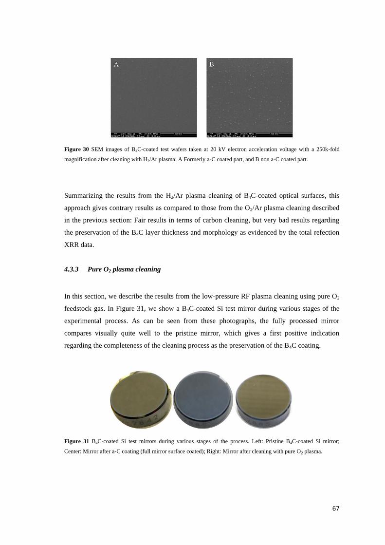
67
Figure 30 SEM images of B4C-coated test wafers taken at 20 kV electron acceleration voltage with a 250k-fold
magnification after cleaning with H2/Ar plasma: A Formerly a-C coated part, and B non a-C coated part.
Summarizing the results from the H2/Ar plasma cleaning of B4C-coated optical surfaces, this
approach gives contrary results as compared to those from the O2/Ar plasma cleaning described
in the previous section: Fair results in terms of carbon cleaning, but very bad results regarding
the preservation of the B4C layer thickness and morphology as evidenced by the total refection
XRR data.
4.3.3 Pure O2 plasma cleaning
In this section, we describe the results from the low-pressure RF plasma cleaning using pure O2
feedstock gas. In Figure 31, we show a B4C-coated Si test mirror during various stages of the
experimental process. As can be seen from these photographs, the fully processed mirror
compares visually quite well to the pristine mirror, which gives a first positive indication
regarding the completeness of the cleaning process as the preservation of the B4C coating.
Figure 31 B4C-coated Si test mirrors during various stages of the process. Left: Pristine B4C-coated Si mirror;
Center: Mirror after a-C coating (full mirror surface coated); Right: Mirror after cleaning with pure O2 plasma.

68
X-ray Photoelectron Spectroscopy (XPS) analysis
In Figure 32, we show the high-resolution C1s and B1s XPS spectra taken off as well as on the
a-C spot before and after the pure O2 plasma cleaning. As can be observed from the C1s spectra,
there is a strong reduction of the C1s lines related to C=O, C-O, and C-C species for both the
“off spot” and the “on spot” spectra due to the plasma cleaning process, whereas the B1s line to
188.3 eV B.E. related to B4C shows up after the plasma treatment. In the case of the B1s
spectra, the “off spot” spectra exhibit a shift of the B1s line to lower B.E. (plus a decrease of the
line width) and the appearance of a small additional peak at about 192.2 eV, that we attribute to
oxidized boron and boron oxy-carbides, respectively
Figure 32 High-resolution C1s and B1s XPS spectra of the B4C-coated test wafer before (black solid lines) and after
pure O2 RF plasma cleaning (red solid lines). Left panel: XPS data taken on the amorphous carbon contamination
spot. Right panel: XPS data taken off the amorphous carbon contamination spot on the bare B4C coating
Figure 33 shows the XPS survey spectra from B4C-coated Si test wafers with the XPS
measurements being performed off as well as on the a-C spot before and after the pure O2
plasma cleaning. The “on spot” spectra give evidence for an efficient removal of the previously
deposited a-C layer based on the significant reduction of the C1s line together with the
appearance of the B1s line from the B4C layer. The same applies to the “off spot” spectra,
although with an obviously less spectacular reduction of the C1s line (as we are dealing with
“off spot” spectra).
Regarding foreign elements, we again note the occurrence of a small amount of Au4f lines that
have been identified as intrinsic to the B4C coating as they are already present in the “off spot”
spectrum of the sample before plasma treatment. It can also be noted that there is no Fe2p line
visible in the survey spectra of the plasma-processed samples. This is in contrast to the previous
section and can be attributed to the fact that there has been no Ar gas added to the pure O2

69
feedstock gas mixture, which would otherwise lead to the aforementioned sputtering
phenomena resulting in the deposition of a small amount of Fe.
Figure 33 XPS survey scans taken from B4C-coated Si test wafers before (solid black lines) and after (solid red lines)
pure O2 plasma cleaning. The left and right-hand side diagram show the XPS spectra taken at a sample location on
and off the amorphous carbon spot, respectively.
X-Ray Reflectometry (XRR) analysis
The measured XRR data in Figure 34 from the formerly fully a-C contaminated test mirror
together with the results from the IMD simulations given in Table 8 fully corroborate the results
from the visual impression by the photographs in Figure 31. As can be seen from the measured
data, the Kiessig fringes throughout the full angular range are maintained and the parameters
resulting from the pertinent IMD simulations yield a slight reduction of the B4C coating
thickness (i.e., 25.5 nm as compared to 26.0 nm) together with an unaltered B4C/air interface
roughness of 0.5 nm rms.
Figure 34 XRR data from B4C-coated test mirror after cleaning with pure O2 plasma cleaning. (red solid lines:
experimental XRR data; black solid lines: IMD simulation).

70
On the other hand, the micro-roughness data from interference microscopy show a substantial
increase from 0.1o to 0.26 nm rms, which is at variance with the results from XRR. We attribute
these contrasting trends to the technical differences between these two surface characterization
techniques that will be discussed in the context of the SEM images.
Table 8 Results from the IMD simulations of the XRR measurements as shown in Fig. 16. (*) Surface roughness
values from interference microscopy
Mirror test sample B4C coating
thickness [nm]
B4C/air interface
rms roughness
[nm]
B4C rms surface
roughness [nm]
After B4C deposition 26.0 ~ 0.5-0.6 0.10
After 7 months in air 27.0 ~ 0.6 --
After pure O2 plasma
cleaning –
a-C coated part
25.5 ~ 0.5 0.26
The XRR total reflection data from a B4C-coated test mirror in Figure 35 give further support
for a full recovery of the B4C surface at negligible losses regarding the integrity of the B4C
layer. The spectrum for the a-C coated (i.e., non-plasma-cleaned) mirror surface shows the
expected chemical and structural deviations in the range from 0.2 to 0.26 degree and beyond
0.26 degree, respectively, due to the additional a-C top layer.
Figure 35 Comparison of XRR total reflection data for a pristine B4C-coated test mirror (black line), after a-C.
Coating (red line), and after subsequent cleaning with pure O2 plasma (green line).

71
On the other hand, the spectrum of the subsequent plasma cleaned sample nicely overlaps with
the spectrum from the pristine untreated mirror in terms of the shape and slope of the reflectivity
edge, beside a small shift regarding the edge position to slightly higher angular values. This
leads to the conclusion for a full chemical and structural recovery of the test mirror from the
perspective of Cu Kα wavelengths and also applies to the optical performance of the fully
processed mirror. Nevertheless, taking into account nowadays B4C optical coating
manufacturing technologies a rms roughness of 0.26 nm appears acceptable.
SEM results
In Figure 36, we show the SEM images of a fully processed B4C-coated test coupon that has
been cleaned with pure O2 plasma. What can be immediately concluded from the images is that
whereas the appearance of the non a-C coated part in Figure 36B is similar to that of the B4C
reference sample in Figure 23A as well as the corresponding images from the other plasma
processed samples in Figures 23C and 30B. In stark contrast to this, the image from the
formerly a-C coated part in Figure 36A exhibits a large density of small structures with
diameters between 15 and 20 nm. As according the XPS results given in Figure 32 the surface
chemistry of the formerly a-C coated part is very similar to the ones from the O2/Ar and H2/Ar
plasma treatment, we conclude that the surface modification in Figure 36A is of a pure
morphological nature, without apparently alternating the surface chemical characteristics that
are basically given by the aforementioned plasma-induced conversion of the B4C and B2O3 bulk
phases into boron oxy-carbides.
As mentioned above, the B4C/air interface roughness as measured with XRR remains
unchanged (see Table 8), whereas the interference microscopy gives an increase from 0.10 to
0.26 nm rms. Taking into account the rather enhanced density of hillocks together with the fact
that XRR is measured at grazing incidence, it seems plausible that interference microscopy
(close to normal incidence) gives the more reliable surface roughness information, consistent
with the SEM results.
Summarizing the results from the pure O2 downstream plasma cleaning, we conclude that this
approach is so far the only promising pathway that leads to an efficient cleaning together with
the desirable preservation of the B4C surface morphology and chemistry, together with a
conservation of the B4C bulk layer thickness. This also applies to the expected optical
performance of the B4C coating as derived from the total reflection data. Nevertheless, the
applied plasma cleaning time still has to be carefully taken into account in view of avoiding an
over-cleaning of the surface coating.

72
Figure 36 SEM images of B4C-coated test wafers taken at 20 kV electron acceleration voltage with a 250k-fold
magnification after cleaning with pure O2 plasma: A Formerly a-C coated part, and B non a-C coated part.
4.3.4 Considerations on a-C plasma cleaning mechanisms and cleaning speed
In table 9, we give a brief summary of the experimentally derived a-C cleaning rates that have
been determined in the present study on a-C contaminated B4C-coated test objects presented
here (extrapolated values) and on Au-coated QCM crystals that have been achieved in previous
studies [1, 2].
As has been observed previously, there is a large difference by roughly a factor of 7 between the
a-C cleaning rates that can be achieved using either O2/Ar or H2/Ar feedstock gases on metallic
substrates. One the other hand, it is clear from these numbers that while going from Au to B4C
coatings, the cleaning rates for the O2 and O2/Ar-based plasma are strongly reduced (roughly by
a factor of 2 to 2.5), whereas the cleaning rates for the H2/Ar-based plasma is basically
maintained.
We basically attribute these changes in a-C cleaning rates for the different substrate coatings –
i.e., more specifically the lowering of cleaning rates for the O2-gas based plasma when going
from Au to B4C coatings – to two different phenomena:
a. The plasma-induced formation of a chemically resilient carbonaceous interface layer on
the sample surface. This is corroborated by the observation of a ubiquitous non-
removable and optically visible residue at the location of the former a-C contamination
and its the resilience and, at the same time, the close similarity of the XPS spectra after
the cleaning process.
b. The fundamentally different processes that lead to the removal of the a-C contamination
as a function of the chemical composition of the plasma feedstock gas. In the oxygen-
rich/argon-poor O2 and O2/Ar plasma, we assign most of the cleaning to the chemical
activity of the oxygen species within the plasma. On the other hand, in the case of the

73
argon-rich H2/Ar plasma, a significant (or could be even dominant) part of the a-C
removal is done via the kinetic effect from the Ar species in the plasma as well as UV
photochemical contributions from an Ar metastable state.
Table 9 Experimentally derived a-C cleaning rates for different types of plasma feedstock gases for both B4C-coated
Si test wafers and Au-coated QCM crystals. All values were measured using 100 W plasma RF power at a plasma
vacuum pressure of 0.005 mbar
Plasma type
and cleaning mechanism
B4C coated test coupons
(this study;
extrapolated)
Au-coated QCM crystal
(previous study*)
Pure O2
(chemical cleaning)
3.5 Å/min. 8.4 Å/min.
O2/Ar
(mostly chemical cleaning)
4.6 Å/min. 11.6 Å/min.
H2/Ar
(mostly kinetic cleaning)
2.3 Å/min. 1.7 Å/min.
The above two phenomena apparently result in the reduction of carbon cleaning rates due to the
chemical resilience of the carbonaceous BOC layer, especially in the case of the chemical
cleaning using the oxygen-based plasma. In contrast to this, the cleaning speed by the argon-
rich H2/Ar plasma is maintained as the kinetic cleaning is kept up also in the case of the carbon-
contaminated B4C-coated optics, which is corroborated by our findings regarding the reduction
of the B4C layer thickness due to the H2/Ar plasma as discussed in section 4.3.2.
The latter does obviously not necessarily exclude the reductive effect of the H• radicals that
could be observed for the cleaning a-C contaminated metal foils, where a reduction of Ni2O3
and Rh2O3 to metallic Ni and Rh could be observed previously. Table 10 shows the
deconvolution of the fitted high-resolution spectra for B1s and C1s for the different plasma
treatments on the Si test wafers.
Our recent results regarding the analysis of the GV10x downstream plasma using Langmuir
probe as well as mass spectroscopy diagnostics indicate that in contrast to prior expectations,
almost no neutral oxygen radicals could be detected in the O2/Ar plasma. Instead, the by far
dominating species consist of ionized oxygen molecules (O2+) and atomic oxygen cations (O+).
Also, the kinetic energies of the argon, hydrogen, and oxygen species involved in the
downstream plasma at 100 W RF power amount to roughly 40 eV. Thus, the future analysis of
the plasma chemistry involved in the removal of the a-C deposits as well as in the
plasma/surface interaction with the B4C layers will have to take into account these findings.

74
Table 10 Deconvolution of the fitted B1s and C1s high-resolution XPS for different surface treatments. All peak
energy and full width at half maximum (FWHM) values are given in eV (“BOC” refers to boron oxy-carbides).
After 10 min
Ar sputtering
After O2/Ar
plasma cleaning
After H2/Ar
plasma cleaning
After O2
plasma cleaning
Peak
assignment
B1s
FW
HM
:1.8
07
188.3 B
1s
FW
HM
1.7
77
188.12
B1s
FW
HM
:1.8
56
188.21
B1s
FW
HM
:1.8
68
188.30
B-B and
B-C in
B4C
189.95 189.49 189.46 189.97 B in
BC2O
191.69 191.40 191.66 192.16 B in
BCO2
193.33 -- -- -- B in B2O3
C1s
FW
HM
1.9
54
282.98
C1s
FW
HM
1.1
616
282.58
&
283.58
C1s
FW
HM
:1.5
66
282.48
&
283.31
C1s
FW
HM
:1.7
40
282.82 C in B4C
284.52 284.94 284.87 284.87 C-C
-- 286.66 286.49 286.71 C-O (e.g.,
in BOC)
-- 288.58 288.50 288.81 C=O
4.4 Chapter Overview
In this chapter, we showed different approaches regarding the chemically selective low-pressure
RF downstream plasma cleaning of B4C-coated and amorphous carbon-contaminated optics by
the variation of the plasma feedstock gas and thus the inherent plasma chemistry. We thereby
also report on the first successful plasma cleaning of such optics, i.e., without incurring damage
of the B4C optical coating and its surface resulting into a fully maintained optical performance.
In more detail, we have performed an extensive test series on various test objects using O2/Ar,
H2/Ar, and pure O2 gas mixtures as plasma feedstock gases in order to determine the optimum
plasma chemistry for the cleaning of B4C optical surface coatings.
Based on our analysis regarding the remote ICP plasma used, we conclude that the O2/Ar
plasma cleaning yields fair results in terms of the preservation of the B4C layer, while the
removal of amorphous carbon contaminations can be considered as poor. On the other hand, the

75
H2/Ar plasma treatment leads to a significant damage of the B4C coating – both regarding the
layer thickness and surface roughness – while the removal of amorphous carbon contaminations
seems to be fairly satisfactory. However, it has to be taken into account that the latter is
apparently an obvious consequence from the former. Last but not least, the plasma cleaning
using pure O2 feedstock gas yields excellent results regarding both the a-C cleaning as well as
the preservation of the B4C layer. We would like to emphasize at this point that other cleaning
approaches may well lead to comparable results regarding B4C cleaning but, to the best of our
knowledge, no pertinent studies can be found in the present literature on this specific topic.
From the above observations, we conclude that the Ar species within the plasma – especially in
conjunction with the reduced a-C cleaning rates and thus enhanced cleaning times of an H2/Ar
plasma – result into sputtering phenomena on the B4C layers that lead to the observed reduction
in layer thickness and enhanced surface roughness. Thus, a pure O2 feedstock gas plasma (i.e.,
without admixture of heavy Ar gas atoms) offers a damage-free and fast cleaning, based on the
chemical activity of the O species. First measurements using plasma mass spectroscopy indicate
that the predominant oxygen species within an O2/Ar feedstock gas plasma consist of O2+
species.
Almost independent from the plasma used, we have observed the formation of a fair amount of
boron oxy-carbides on the B4C surfaces that presumably appear as hillocks on these surfaces
and thus contribute to the surface micro-roughness. This especially applies to the H2/Ar plasma-
cleaned test samples. The formation of this chemically rather resilient carbonaceous layer could
be observed both visually as well as based on XPS data and appears to contribute to the required
extended cleaning times as compared to, e.g., the cleaning of metallic optical coatings. We
conjecture that the formation of this surface boron oxy-carbide layer is the result from the
surface interaction of the plasma with the B2O3 and B4C phases inherent to the bulk of the B4C
coating, resulting into the formation of the said surface boron oxy-carbides.
The apparent sensitivity of the B4C layers with respect to a plasma-induced damage (i.e., as
compared to apparently less sensitive metallic optical coatings) emphasizes the importance of an
in-situ monitoring of the cleaning process in view of avoiding a cleaning process beyond the
time required for the full removal of the carbon contaminations. To this end, an optical in-situ
endpoint detection scheme is presently under development that allows monitoring the progress
of the cleaning process in order to stop the treatment once a clean optical surface has been
achieved.

76

77
Chapter 5
5 Towards Chemically Neutral Carbon Cleaning Processes: Plasma
Cleaning of Ni, Rh, and Al Reflective Coatings and Thin Al EUV
Filters for Free Electron Lasers and Synchrotron Beamline
Applications
In this chapter will be introduced a study regarding the low-pressure RF ICP plasma cleaning by
using two different gas mixture configurations, N2/O2/H2 and N2/H2. The goal consists on the
carbon removal in a safe efficient and well-understood way of three different materials Ni, Rh,
and, Al plus a subsequent cleaning of Al EUV filters previously used at the FERMI FEL by
using a N2/H2 plasma.
The justification of the choice of kind of gas arises from the results obtained in a previous study
[2] where a complete analysis on the plasma cleaning was done on Ni, Au, and Rh by using
Ar/O2 and Ar/H2. Those results show that Rh and Ni will oxidize and reduce in the presence of
oxygen and hydrogen in the plasma, while Au due to its nature will remain inactive.
In addition, by using N2/H2 as feedstock gasses the desire also was to increase the cleaning rate
in front the Ar/H2 mixture and thus speed-up the cleaning rate.
5.1 Opening
Rh, Ni, and Al among other materials, are the most common optical coatings used for
synchrotron mirrors, due to their good reflectance. Aluminum is the most commonly used
material for EUV and soft X-Ray filters due to its excellent mechanical properties, thermal
conductance, and wide photon energy bandpass while blocking –among others-the visible light.
However, reflective optics and transmission filters are subjected to carbon contaminations
buildup, where the latter represents an increasingly serious problem for the operation of high-
performance synchrotron and FEL beamlines. As already was mentioned and showed, these
carbon contaminations can be removed by using a different kind of plasmas getting different
results depending on the gas mixture, input power, frequencies and surfaces to be cleaned. In

78
this vein and following previous studies [1,2,39], the ICP-type model ibss GV10x low-pressure
plasma source together with N2/O2/H2 and N2/H2 feedstock gases has been used to clean Ni, Rh,
and Al foil materials and ultrathin Al filters for Extreme Ultra-Violet (EUV) applications.
Using XPS, we show changes in the surface chemistry of the various above metals before and
after the different plasma treatments. In addition, results from the successful carbon cleaning of
ultrathin Al EUV filters used at the FERMI FEL1 [40] are presented.
5.2 Experimental Description
A set of Ni, Rh, and Al metal foils with micrometric thickness were contaminated with 50 nm of
amorphous carbon (a-C) for simulating a photon-beam induced carbon contamination (see
Figure 37). On the other hand, the self-sustained ultrathin Al filters (Luxel Corporation, Friday
Harbor, WA, USA) with 100 nm thickness were contaminated by exposure to the FEL photon
beam operation at the FERMI FEL1. All samples were plasma cleaned in an ultra-high vacuum
(UHV) chamber (Figure 8), where the base pressure was 1.9x10⁻⁸ mbar.
The plasma operating pressure was kept at 0.005 mbar (3.75 mTorr) for both
N2(94%)/O2(4%)/H2(2%) and N2(95%)/H2(5%) feedstock gas mixtures supplied via commercial
pre-mix gas bottles (Air Liquide). Both gases will be referred to as N2/O2/H2 and N2/H2 from
now on. The plasma feedstock gas pressure was kept constant at 0.005 mbar, which corresponds
to best cleaning rates that can be obtained when cleaning carbon contaminations on optical
components in our setup with the above feedstock gasses. The RF power of the ICP plasma
source was maintained at 100 W.
The plasma source consists of the ibss model GV10x described in section 1.3.1. Notice this
plasma source generates a downstream plasma product of the differential pressure between the
plasma tube pressure and the plasma chamber pressure. The Downstream Asher operation
principle allows for generating the plasma in a separate “remote plasma” volume upstream the
UHV chamber including the plasma diagnostics and the optical objects to be cleaned. With the
plasma source being localized outside the main chamber, the ionization of the different gasses
will only take place within the upstream plasma source. The a-C cleaning rate – as measured by
a quartz balance - obtained was 7.2 Å/min and 2.5 Å/min for N2/O2/H2 and N2/H2 plasma,
respectively. This significant difference in terms of carbon cleaning rate is related to the small
oxygen percentage in the former gas mixture. Differences in terms of cleaning rate were already
observed in previous studies [1, 2, and 20]
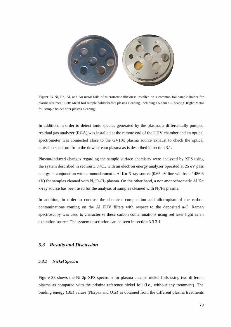
79
Figure 37 Ni, Rh, Al, and Au metal foils of micrometric thickness installed on a common foil sample holder for
plasma treatment. Left: Metal foil sample holder before plasma cleaning, including a 50 nm a-C coating. Right: Metal
foil sample holder after plasma cleaning.
In addition, in order to detect ionic species generated by the plasma, a differentially pumped
residual gas analyzer (RGA) was installed at the remote end of the UHV chamber and an optical
spectrometer was connected close to the GV10x plasma source exhaust to check the optical
emission spectrum from the downstream plasma as is described in section 3.1.
Plasma-induced changes regarding the sample surface chemistry were analyzed by XPS using
the system described in section 3.3.4.1, with an electron energy analyzer operated at 25 eV pass
energy in conjunction with a monochromatic Al Kα X-ray source (0.65 eV line widths at 1486.6
eV) for samples cleaned with N2/O2/H2 plasma. On the other hand, a non-monochromatic Al Kα
x-ray source has been used for the analysis of samples cleaned with N2/H2 plasma.
In addition, in order to contrast the chemical composition and allotropism of the carbon
contaminations coming on the Al EUV filters with respect to the deposited a-C, Raman
spectroscopy was used to characterize these carbon contaminations using red laser light as an
excitation source. The system description can be seen in section 3.3.3.1
5.3 Results and Discussion
5.3.1 Nickel Spectra
Figure 38 shows the Ni 2p XPS spectrum for plasma-cleaned nickel foils using two different
plasma as compared with the pristine reference nickel foil (i.e., without any treatment). The
binding energy (BE) values (Ni2p3/2 and O1s) as obtained from the different plasma treatments

80
are reported in table 11. After the cleaning process using N2/H2 plasma, no changes were
observed regarding the Ni chemical state in both the native oxide surface layer as well as the Ni
metal foil bulk, unlike expected and based upon previous studies [2], where hydrogen-based
Ar/H2-plasma had resulted in a significant reduction of the native Ni2O3 surface layer of the Ni
foil.
Figure 38 Ni 2p (left column) and O 1s (right column) XPS core level spectra of Ni metal foils. Bottom row: Pristine
Ni reference sample; Center row: Ni foil after a-C contamination and subsequent N2/O2/H2 plasma treatment; Top
row: Ni foil after a-C contamination and subsequent N2/H2 plasma treatment
In addition, as the intensity ratio between the Ni 2p3/2 lines for both Ni in Ni2O3 and Ni metal
remains unchanged, the thickness of the former native oxide layer appears to be unchanged.
Regarding the O1s XPS core level data, the peak corresponding to Ni2O3 for the plasma treated

81
foil appears to be not as well-defined as in the case of the Ni reference foil, most probably due
to the non-monochromatic Al Kα source used in the former case.
However, when using the N2/O2/H2 plasma the Ni2p3/2 spectrum shows a change towards a
more complex structure with intense satellite lines at a higher binding energy corresponding to
the cd8 and cd9L plus the cd10L2 XPS final states, respectively. The Ni2p3/2 line gives two
different species at binding energies (BEs) of 853.58 and 855.71 eV as compared with the Ni
reference foil, apparently induced by the N2/O2/H2 plasma treatment now including a small
oxygen concentration. On the basis of their BEs, we assign these peaks to NiO and NiOOH,
respectively, which is in agreement with previous studies [41, 42].
The O1s XPS spectrum gives four different peaks for all samples, although the spectrum from
N2/O2/H2 plasma-treated foil shows appreciable variations. Taking into account these changes,
these spectral features can be assigned to different species and the associated BE positions are
as follows: 529.06, 530.68, and 531.68 eV for NiO, C-C, and C-O respectively.
5.3.2 Rhodium Spectra
Figure 39 shows the Rh 3d XPS spectra for the a-C contaminated and subsequently plasma-
cleaned rhodium metal foils with two different plasmas as compared with a pristine reference
rhodium foil (i.e., without any treatment). In the case of rhodium, we observe a similar behavior
as in the case of nickel after N2/H2 plasma treatment, where chemical changes could not be
observed in contrast to prior expectations based on previous studies. Although the peak position
attributed to Rh2O3 oxide is shifted by 0.67 eV to higher BE in comparison with the Rh2O3
oxide from the reference foil (due to the lack of spectral features that would allow for a better
fitting). The reference Rh 3d spectra were fitted with two main peaks at binding energies of Rh
3d5/2 at 307.04 and 307.6 eV for metallic Rh and Rh2O3, respectively.
The BEs of Rh metal and Rh2O3 oxide after the N2/H2 plasma treatment are in fair agreement
with the values obtained by Kibis et al.[43] for metallic Rh0 and Rh3+ in Rh2O3 respectively,
where peak positions at 307.3 and 308.2 eV, respectively, were obtained. As in the case of the
N2/H2 plasma-treated Ni foil (Figure 38, right column), the N2/H2 plasma-treated Rh foil
exhibits slightly broader spectral lines due to the use of a non-monochromatized Al Kα source.
After the N2/O2/H2 plasma treatment, a clearly enhanced oxidation of the Rh foil can be
observed from the increase of the Rh2O3-related Rh5/2 peak at 307.93 eV BE (Figure 39). The
O1s spectrum now shows four features: The peak formerly observed on the Rh reference foil as
well as the N2/H2 plasma-treated Rh foil at 529.68 eV, plus additional peaks at 531.32, 532.49

82
and 534.35 eV BE. We attribute those additional peaks to Rh2O3, rhodium hydroxide groups
[43-45], carbonates and adsorbed H2O. In this vein, we associate the Rh 3d5/2 peak at 309.59 eV
with rhodium hydroxide group.
Figure 39 Rh 3d (left column) and O 1s (left column) XPS core level spectra of Rh metal foils. Bottom row: Pristine
Rh metal reference sample; Center row: Rh foil after a-C contamination and subsequent N2/O2/H2 plasma treatment;
Top row: Rh foil after a-C contamination and subsequent N2/H2 plasma treatment.
At variance with the previous study by Kibis et al.[43], where RhO2 peaks were found after
plasma sputtering and characterized in terms of an additional O1s line at 530.6 eV BE, we could
not detect such a feature at this BE position in our O1s XPS spectra. Nevertheless, the
spectroscopy data on RhO2 are a bit contradictory due to the Rh4+O2 in the Rh5/2 core-level line
has been reported to be in a range of 309-310 eV, which in the case of our N2/O2/H2 plasma
treatment corresponds to a peak position at 309.59 eV. In that sense, we attribute the O1s line at
531.32 eV and the Rh3d5/2 line at 309.59 eV as Rh4+/Rh3+-based rhodium oxyhydroxide species.

83
5.3.3 Aluminum Spectra
Taking into account the results from the previous cleaning processes, where – besides the
expected significant a-C contamination removal – only the N2/H2 plasma appears to leave the
surface chemistry unchanged, we thus performed only a N2/H2 plasma cleaning process on the
Al foils. In this way, we avoid a further oxidation of the Al foil surface beyond the native Al2O3
layer, together with a possible mechanical destabilization via the formation of that brittle oxide.
The detailed Al 2p and O1s core level spectra are shown in Figure 40, for Al metal foils before
and after a-C contamination plus subsequent N2/H2 plasma treatment. In both cases, the metal
peaks corresponding to the Al 2p3/2 and 2p1/2 core level lines can be seen at 72.53 eV and 73.19
eV BE, respectively, while the peak at 75.47 eV is related to the Al2O3 surface layer.
Figure 40 Al 2p (left column) and O 1s (right column) XPS core level spectra of Al metal foils. Bottom row: Pristine
Al reference sample; top row: Al foil after a-C contamination and subsequent N2/H2 plasma treatment.
These spectral features are in good agreement with values found in the standard web-based XPS
literature [46] for Al oxide on Al foil. However, in contrast to values reported in the literature
[47, 48], none of the oxides show an O1s peak in the typical oxide region between 529-530eV,
even more, the values obtained are ~1eV shifted from values found in the literature.

84
The O1s peak is relatively broad and symmetric; its deconvolution shows two components for
the reference foil as well as for the plasma-treated Al foil with two peaks at BEs of 532.21 and
533.45 eV. In the case of plasma-treated Al foil, a clear difference in the ratios of these two
components can be seen. The peak at 532.21 eV BE related to Al2O3 increases after plasma
treatment, indicating an increase of the oxide thickness. This assumption can easily be
corroborated using the calculations of the type developed by Strohmeier [49], yielding a small
increase of the oxide thickness. From the O1s spectra in Figure 40, it can also be seen that there
is a decrease of the carbon-oxygen C=O-related line at 533.45 eV BE.
5.3.4 Al EUV Filter Cleaning
Taking into account the above results regarding the performance of the N2/H2 plasma and
especially its interesting feature on the preservation of the original surface chemistry of the
plasma-processed metal foils, one can conclude that this process would be sufficiently safe for
the carbon contamination cleaning of the corresponding thin filter foils. Here, besides restoring
the original optical performance of the pure metal filter material the preservation of the
mechanical integrity of these devices is of importance. Thus, avoiding an increase of the native
Al2O3 surface layer thickness is of importance for both the optical as well as the mechanical
performance of these self-sustained ultrathin Al filter foils.
We have thus performed a N2/H2 plasma cleaning on a set of Al EUV foil filters that have been
exposed for roughly 500 operation hours to the pulsed high brilliance photon beam of the
FERMI FEL1 in a photon energy range of 20 to 65 eV photon energy. The results from the
above plasma cleaning process are shown in Figure 41. As can be seen, a successful carbon
removal was obtained on the considerably more carbon contaminated filter upstream side. An
additional interesting feature consists of the fact that the carbon-contaminated Al filter foils
exhibit a wrinkled appearance at the position of the carbon footprint (Figure 41A).
On the other hand, after cleaning the surfaces of the filter does not show these wrinkles any
further. We conclude from this that the foil wrinkles do result from the fact that the carbon layer
is deposed onto the Al metal with the latter being at elevated temperatures during the photon
beam exposure. After cooling down, the difference in linear thermal coefficients between these
two materials (aluminum: 21 to 25 x 10-6 m (m K)-1; graphite: 4 to 8 x 10⁻⁶ m (m K)-1; RT
values) results in the observed formation of wrinkles associated with mechanical stress at the
carbon/Al interface. Thus the removal of the carbon footprint simultaneously does remove the
observed wrinkles within the Al filter foils, becoming stress-free again.
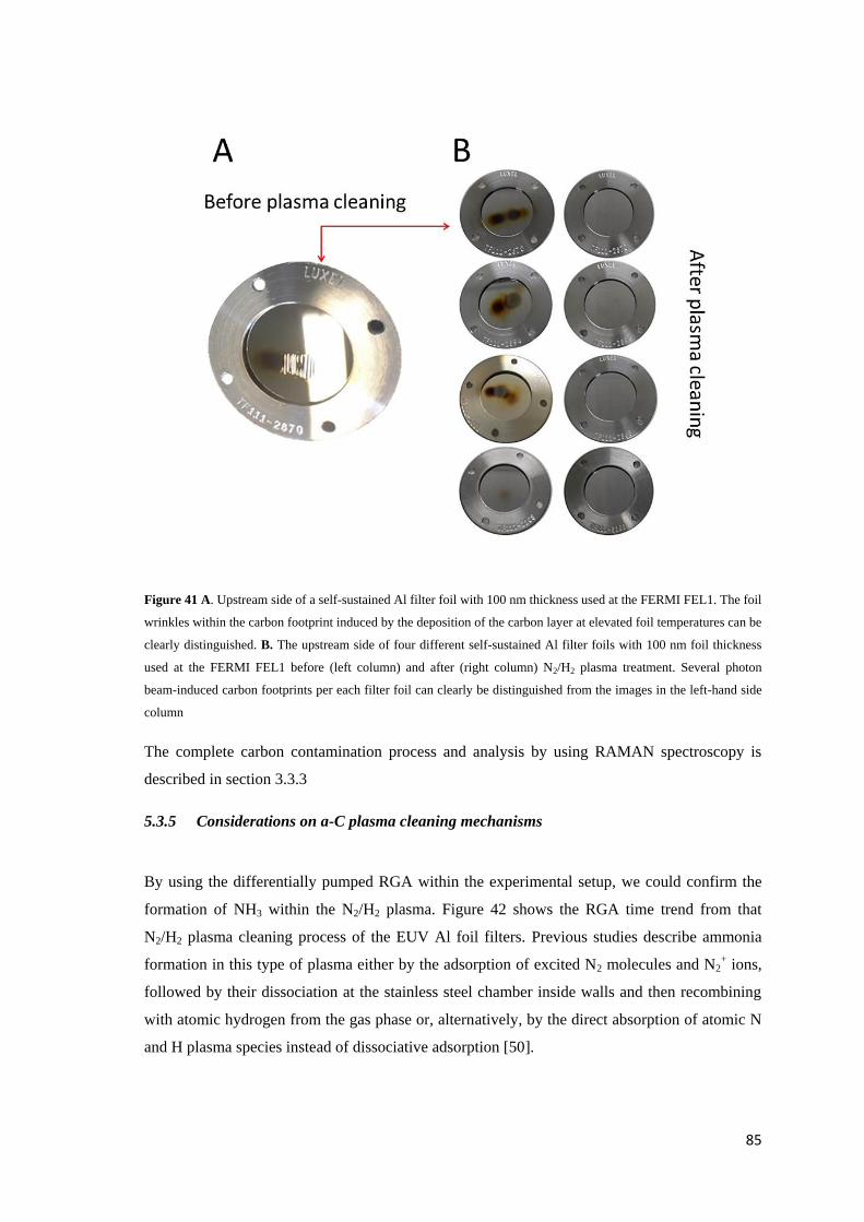
85
Figure 41 A. Upstream side of a self-sustained Al filter foil with 100 nm thickness used at the FERMI FEL1. The foil
wrinkles within the carbon footprint induced by the deposition of the carbon layer at elevated foil temperatures can be
clearly distinguished. B. The upstream side of four different self-sustained Al filter foils with 100 nm foil thickness
used at the FERMI FEL1 before (left column) and after (right column) N2/H2 plasma treatment. Several photon
beam-induced carbon footprints per each filter foil can clearly be distinguished from the images in the left-hand side
column
The complete carbon contamination process and analysis by using RAMAN spectroscopy is
described in section 3.3.3
5.3.5 Considerations on a-C plasma cleaning mechanisms
By using the differentially pumped RGA within the experimental setup, we could confirm the
formation of NH3 within the N2/H2 plasma. Figure 42 shows the RGA time trend from that
N2/H2 plasma cleaning process of the EUV Al foil filters. Previous studies describe ammonia
formation in this type of plasma either by the adsorption of excited N2 molecules and N2+ ions,
followed by their dissociation at the stainless steel chamber inside walls and then recombining
with atomic hydrogen from the gas phase or, alternatively, by the direct absorption of atomic N
and H plasma species instead of dissociative adsorption [50].

86
Therefore, we can attribute the cleaning process mainly to the ammonia In the case of N2/H2
plasma, arguing that NH3 will reduce the carbon contamination, the cleaning rate thereby not
only depends on the total pressure (via mean the corresponding free path lengths) but obviously
also on the ammonia production rate/concentration within the plasma. Decomposition of the
hydrocarbon molecules takes place by breaking the C-H strong chemical bonds
In the case of N2/O2/H2 plasma not only the ammonia is the responsible for the cleaning process
but the small oxygen amount added to the mixture that boosts the cleaning rate by forming
volatile compounds as CO and CO2.
Figure 42 RGA time trend from the N2/H2 plasma during the plasma cleaning of the EUV Al foil filters. The
complete time span of the RGA trend plot corresponds to about 4 hours and 50 minutes.
According to the above and as can be seen from Figure 42 the ignition of the plasma (at the time
of scan 20) results in the formation of NH3 species together with corresponding NH2 and NH
cracking products that also vanish once the plasma is stopped (at the time of scan 173). The
gaseous reaction products from the interaction between the carbon and the ammonia species
equally do show the same dependence on the plasma operation, as the ethane (mass 30) and
propane (mass 44) mass trends appear and disappear with the plasma being on or off,
respectively (see the read markups in Figure 42).

87
From the decrease of these two-time trends during while the plasma is operative, one can
conclude on the depletion of carbon species within the plasma chamber as a function of the
plasma operation time.
Figure 43 C1s for the different materials after the carbon contamination and subsequent plasma cleaning. Left
column Rh as reference sample, after N2/O2/H2 plasma (center) and after N2/H2 plasma (bottom). Center column Ni
and right column Al as reference material and after N2/H2 plasma.
Figure 44 N1s XPS for Rh, Ni, and Al materials after N2/H2 plasma cleaning.

88
Table 11 XPS core level binding energies as obtained from the XPS spectra presented in Figures. 38 to 40, 43, and
44.
XPS line Reference foil
B. E. (eV)
N2/O2/H2 Plasma
B. E. (eV)
N2/H2 Plasma
B. E. (eV)
Ni metal foil
Ni2p 852.08 Metal 852.1 Metal 852.08 Metal
855.36 Ni2O3 853.58 NiO 855.41 Ni2O3
855.71 NiO (+ NiOOH)
O1s 529.02 Ni2O3 529.06 NiO 529.01 Ni2O3
530.84 C-C 530.68 C-C 530.93 C-C
531.67 O-H, O with C 531.68 O-H, O with C 531.88 O-H, O with C
532.93 532.68 533.32 Nitrates
C1s 284.6 C-C 284.46 C-C 284.52 C-C
286.03 C-OH 286.1 C-OH 286.18 C with N
288.16 C-OH 287.93 Cyanides 287.98 Cyanides
289.2 Carbonates 289.17 Carbonates 289.05 Carbonates
Rh metal foil
Rh 3d 307.04 Metal 307.06 Metal 307.05 Metal
307.60 Rh2O3 307.93 Rh2O3 308.27 Rh2O3
309.59 RhOOH
O1s 529.52 Rh2O3 529.68 Rh2O3 530.23 Rh2O3
531.59 Carbonates 531.32 RhOOH 532.07 Carbonates
532.49 Carbonates
534.35 Absorbed H2O
C1s 284.64 C-C 284.53 C-C 284.78 C-C
286.19 C-OH 286.01 C-OH 286.5 C with N
288.13 C-OH 288.04 Cyanide 288.28 Cyanide
Al metal foil
Al 2p 72.53 Metal 2p3/2 72.5 Metal 2p3/2
73.19 Metal 2p1/2 73.1 Metal 2p1/2
75.47 Al2O3 75.41 Al2O3
O1s 532.21 Al2O3 532.21 Al2O3
533.45 C=O 533.52 C=O
C1s 285.88 C-C 285.39 C-C
287.41 C-OH 287.19 C-OH
289.97 Carbonates 289.58 Cyanide
Decomposition of the hydrocarbon molecules takes place by breaking the C-H strong chemical
bonds. The reactions forming free carbon atom also could be possible according to the study by
Ciobotaru et al., [51] where there is a direct formation of CN, CN2 or HCN molecules.

89
The Hydrogen cyanide (CNH) reaction can be promoted by the interaction of hydrogen, carbon
and nitrogen compounds according to the following reaction [52]
2𝐶 + 𝐻2 + 𝑁2 → 2𝐻𝐶𝑁 (19)
In addition the carbon molecules can react directly with nitrogen atoms via the reaction
𝑁 + 𝐶2 → 𝐶𝑁 + 𝐶, this was already observed in previous experiments in which there was not
used hydrogen in the mixture, although the cleaning rate was lower for this plasma with pure
nitrogen gas as can be observed in table 12.
C1s resolved spectra of the different materials and plasmas were analyzed, as shown in Figure
43. The cyanide CN- was detected between 288.28 and 289.58 eV depending on the material,
the corresponding values can be seen in table 11. N1s peak only was detected on samples
cleaned with N2/H2 plasma as cyanide and azide (NN*N) molecules (see Figure 43).
5.3.6 Summary
Summarizing, we conclude that a favorable combination of a N2(95%)/H2(5%) plasma
feedstock gas mixture leads to the best chemical surface preservation results for non-inert metal
optical coatings such as Ni, Rh, and Al together with the removal of carbon contaminations and
including an acceptable carbon cleaning rate. However, the above feedstock gas mixture does
not remove carbon contaminations as fast as, e.g., a N2(94%)/O2(4%)/H2(2%) plasma which, on
the other hand, induces the surface formation of NiO and NiOOH in Ni and RhOOH in Rh foils.
Thus, the application of a specific gas mixture for low-pressure RF plasma has to be considered
on the background of the beamline optics requirements. It should be emphasized in this context
that the above metal surface preservation has been demonstrated for the specific cases of Rh, Ni,
and Al and cannot be necessarily be transferred directly to other metals without prior testing.
As an application of the above N2(95%)/H2(5%) plasma, we could demonstrate a first efficient
ex-situ carbon cleaning process of self-sustained thin Al foil optical filters (100 nm thickness)
as a specific case study within the field of transmission optics for FEL application in the EUV
photon energy range. As a peculiar side effect, macroscopic wrinkles in the Al foil located
within the carbon footprint were removed simultaneously.

90

91
Chapter 6
6 PLASMA DIAGNOSTICS
The aim of this chapter is to present the results from an analysis carried out on the plasma
produced by an ibss model GV10x downstream plasma source typically use in our experiments
om the cleaning of carbon-contaminated optics. The spatial ion energy distribution was
measured using a quadrupole mass spectrometer at different RF powers as well as different
distances from the plasma source. In addition, a Langmuir probe system allows measuring the
characteristic plasma parameters for each gas mixture. The motivation to perform such analysis
arises from the need to identify the different processes involved during the plasma cleaning, i.e.,
physical sputtering, chemical cleaning or a combination of both.
6.1 Introduction
Plasma treatments are emerging as treatments with superior efficiency for large surface areas; in
a recent paper, the authors studied the changes in terms of surface chemistry of carbon
structures after Ar, O2/Ar, H2/Ar and CO2 plasmas. They reported that in the case of a H2/Ar
plasma, there is a decrease in sp2 bonds in the carbon structure while O2/Ar plasma leads to the
highest reduction is sp3 bonds [53].
In this work, a movable QMS detailed in section 3.3.1.1 was used to investigate the IEDs for
H+, H2+, H3
+, Ar+, ArH+, O+, and O2+ ions in Ar, H2/Ar, and O2/Ar low-pressure remote
inductively coupled plasmas (r-ICP). In addition, a movable Langmuir Probe system (LP)
described in section 3.3.2.1 has been used that allows us to calculate individual electron
currents, ion currents, plasma potentials, and electron temperatures.
6.2 Experimental Setup
The plasma diagnostics was carried out in a horizontal chamber of cylindrical shape made of
304L stainless steel, an 80l/s turbo-molecular pump unit was installed in order to keep a base
pressure of 6.5 x 10⁻⁸ mbar. The pressure inside the chamber is controlled by using a flow meter
gas supply system described in section 3.1. The operating pressure is kept at 0.003 mbar for

92
O2/Ar plasma with a feedstock gas ratio of 85/15, the same way for H2/Ar with a ratio of 65/35
at a pressure of 0.0025mbar and Ar plasma feedstock gas pressure of 0.0016 mbar. The reason
for such pressure and gas ratio values is related to best cleaning rates that can be obtained when
cleaning carbon contaminations of optical components. The RF power is varied from 100W to
300W.
As already mentioned, due to the fact that the GV10x plasma source is located outside the main
chamber, the ionization of the different gases will only take place inside the plasma source so
that this geometry establishes a gradient of the plasma density, which will decrease from the
plasma source up to the back end of the chamber where the plasma gradient will be
accompanied by a gradient on the electron density as well as the plasma potential. Therefore, by
modifying the plasma potential the electron temperature and the plasma sheath will be modified
as well. A circular LP system situated at d1 = 250 mm, d2 = 350 mm and, d3 = 450 mm in the
axial direction from the plasma source was used. In a further experiment, the LP probe was
installed in a plane perpendicular to the plasma source axis at 350 mm distance from the latter
as can be seen in the scheme of the experimental set-up in Figure 45.
Figure 45 Plasma diagnosis chamber.
The QMS was connected at the back end of the chamber in order perform the ion energy
analysis and determine the ion energy distribution functions (IEDs). The MS is operated in

93
positive ion detection mode which performs the energy scanning at a fixed, but variable ion
mass.
In this analysis single and double Langmuir probes were used. Details about this device can be
found elsewhere [54]. Two tungsten probe tips (diameter 100 µm, length 8 mm, parallel
displacement 7 mm) were located at the front side of the LP probe.
6.3 Results and Discussion
Figure 46 shows the plasma diffusion inside the chamber where the plasma produced by the ICP
source expands as the applied plasma power increases. Hence, a non-uniform situation due to
the high plasma gradients present inside the chamber can be expected for the analysis.
As the analysis is done with two different devices (LP and QMS) it is important to take into
account this gradient and the way how each device collects the plasma particles (see the red
arrows in Fig. 46).
Figure 46 Plasma gradient distribution inside the chamber.
6.3.1 Non-Maxwellian Characterization
For the single-probe measurements the Druyvesteyn’s method has been used. The electron
energy probability function 𝑓(𝐸) is directly obtained from the second derivative of the current–
voltage characteristic, therefore

94
𝑓(𝐸) =(8𝑚𝑒)1/2
𝑒3𝐴 𝑑2𝐼
𝑑𝑉2 (20)
Where 𝐸 = 𝑒(𝑉𝑝 − 𝑉) is the electron energy, 𝑉𝑝 and 𝑉 are the plasma potential and probe
potential, respectively, 𝑚𝑒 is the electron mass, 𝐼 is the probe current, and 𝐴 is the probe area.
The electron energy distribution function 𝐹(𝐸) is related to 𝑓(𝐸) by
𝐹(𝐸) = 𝐸1
2𝑓(𝐸). (21)
The electron density 𝑛𝑒 and temperature 𝑇𝑒 are then calculated by
𝑛𝑒 = ∫ 𝐸1
2𝑓(𝐸)𝑑𝐸∞
0 (22)
and,
𝑘𝑇𝑒 =2
3𝑛𝑒∫ 𝐸
3
2𝑓(𝐸)𝑑𝐸∞
0 (23)
6.3.2 Maxwellian Characterization
Langmuir single probe
Considering electrons having a Maxwellian velocity distribution, the electron current at a given
probe potential 𝑉 is obtained by
𝐼𝑒 = 𝑒𝑛𝑒𝐴 (𝑘𝐵𝑇𝑒
2𝜋𝑚𝑒)1/2
𝑒𝑥𝑝 [𝑒(𝑉−𝑉𝑝)
𝑘𝐵𝑇𝑒], (24)
where 𝐼𝑒 is the electron current, 𝑛𝑒 the electron density, 𝑇𝑒 the electron temperature, 𝑚𝑒 the
electron mass, 𝑉𝑝 the plasma potential and 𝐴 the collection probe surface area, 𝑒 the electron
charge and 𝑘𝐵 the Boltzmann constant. The ion saturation current 𝐼𝑠 is given by
𝐼𝑠 = 0.5𝑒𝑛𝑖𝐴 (𝑘𝐵𝑇𝑒
𝑚𝑖)1/2
, (25)
where 𝑛𝑖 is the ion density and 𝑚𝑖 the ion mass. The combination of equations (24) and (25)
describes the total current collected by the Langmuir probe. In this work, the total current is
described by four parameters (𝐼𝑠, 𝑅, 𝑉𝑓 , 𝑇𝑒), R takes into account a variation of the effective
collection area, in our case this is due to the long size of the probe tips (8 mm). Using the
procedure described by Brockhaus et al. [55] 𝑛𝑖 , 𝑇𝑒, and 𝑉𝑝 were determined.

95
A first use of this procedure gives us information about the values of 𝑉𝑓 and 𝑉𝑝 that can be used
in the non-Maxwellian approximation described previously.
Langmuir Double probe
For the double-probe current-voltage characteristics, the evaluation of the plasma parameters as
electron temperature and ion density is performed in the following way: From a typical current-
voltage characteristic, as shown in Figure 47, the slopes of the three linear sections and the
saturation current were read. Electron temperature 𝑇𝑒 and, ion density ni were calculated
according to [55, 56]
𝑘𝑇𝑒
𝑒=
𝐼𝑖,𝑠𝑎𝑡
2(𝑑𝐼
𝑑𝑉)𝑉=0
− 1
2(𝑑𝐼𝑖,𝑠𝑎𝑡,1
𝑑𝑉+
𝑑𝐼𝑖,𝑠𝑎𝑡,2𝑑𝑉
) , 𝑛𝑖 =
𝐼𝑖,𝑠𝑎𝑡
𝐴𝑒√𝑘𝑇𝑒𝑀
(26)
Where A is the probe tip area and M the ion mass.
Figure 47 Double-probe current-voltage characteristics for an Ar plasma at 300 W RF power at d1 axial position.
6.3.3 Ion Energy Distributions (IEDs)
Figure 48 shows the IEDs in a H2/Ar plasma at different RF powers and at distances d1 and d2
from the plasma source. The IED for each of the Ar+, ArH+, H+, H2+, H3
+ ions is shown. The
energy distribution is broad for all 5 species in this plasma. At 100W for Ar+ the IED peak is

96
clearly mono-energetic and tends to split when increasing the input power shifting to higher
energies and broadening by ~5 eV when going from 48 eV to 52.6 eV while, at the same time,
getting lower in intensity. The ArH+ ions show a similar behavior, but this time with almost the
half of the count rate.
Table 12 Summary of the mean ion energies for the different plasma configurations.
Ion type Rf power (W) Energy (eV)
250 mm
Energy (eV)
350mm
Ar+ in Ar plasma 100 34.1
200 37.9
300 38.3
Ar+ in H2/Ar plasma 100 48.1 39.6
200 50.9 44.3
300 52.6 46.9
ArH+ in H2/Ar plasma 100 49 42.4
200 51.8 46.2
300 53.6 48.8
H3+ in H2/Ar plasma 100 50.8 42.6
200 56.1 47.2
300 59.1 50.2
H2+ in H2/Ar plasma 100 51.6 43.1
200 56.7 48.2
300 59.2 51.3
H+ in H2/Ar plasma 100 50.8 44.6
200 56.6 51.7
300 59.2 53.4
Ar+ in O2/Ar plasma 100 40.8 34.2
200 42.9 36.8
300 43.8 38.6
O2+ in O2/Ar plasma 100 40.5 33.2
200 42 35.6
300 43.5 42.85
O+ in O2/Ar plasma 100 42/61 36.9/59.8
200 43.7/63.5 39.3/64.4
300 45.6/66.8 40.9/65.9
Ar0 in Ar plasma 100 2.3
200 2.2
300 2.2

97
The mean ion energy for all ions in the different plasma configurations was calculated according
to Gudmundsson [57] as:
𝜀̅ =∫ 𝜀𝑓(𝜀)𝑑𝜀
∫𝑓(𝜀)𝑑𝜀 (20)
Where 𝑓(𝜀) is the corresponding IED. Table 12 shows the mean ion energy 𝜀 ̅for the different
ion species in the plasma.
In the case of H+, H2+, H3
+ the behavior of the IEDs is different. In these cases, the IEDs show a
well-defined bimodal structure. This broad and bimodal structure is determined by the time
taken by the ions over the RF period wrf/w; in a sense, it is the result of how the ions respond to
the instantaneous sheath voltage when crossing the sheath, which means these two energy peaks
depend on the sheath potential phase (maximum or minimum potential) [58, 59].
Figure 48 IEDs for H3+, H2
+, H+, Ar+ and ArH+ in a H2/Ar plasma at different RF powers and two MS to source
distances. At the top left the corresponding mass scan can be seen.

98
When the RF power increases from 100W to 300W, the mean ion energy increases, while
simultaneously the position of the two prominent peaks in the IEDs spread to lower and higher
energies, respectively. Increasing the RF power causes the average voltage drop across the
sheath to increase by ~5 eV for those three hydrogen ions. Let’s name E1 and E2 as the energies
of the two prominent peaks in the IEDs for H+, H2+and, H3
+ions in the plasma, then, the average
voltage drop can be determined by Vd= (E1+E2)/2e.
In addition, it can clearly be seen that at a larger distance of 350 mm the IED peaks become
narrower and mono-energetic, shifting to lower energies and decreasing in intensity. According
to the raw count rates, the dominant ions in the H2/Ar plasma are the Ar+, H3+, and H2
+ species,
which indicates that the plasma chemistry is independent of any mass-dependent flow rate.
Figure 49 IEDs for O2+, O+, and Ar+ in O2/Ar plasma at different RF powers and two distances. At the top left the
corresponding mass scan is shown.
In the case of an O2/Ar plasma, the IEDs shows a nearly mono-energetic peak with a broad low-
intensity structure at roughly 60 eV kinetic energy for the O+, O2+ and Ar+ ions found in this
plasma at a different RF powers and distances (see Figure 49). This time, the main peak on the
IEDs at about 45 eV kinetic energy can be understood as thermalized (secondary) ions near the
entrance orifice of the MS. This main peak correlates with the plasma potential as the plasma
potential decreases when moving the MS away from the plasma source (see Figure 50) - so do
the energy peaks in the IEDs move to lower energies. On the other hand, the broad low intensity

99
structures at higher energies are related to "ballistic", i.e., non-thermalized ions reaching the MS
entrance orifice that do not show a distinct dependence from the source-probe distance.
Figure 50 Plasma potential gradients in the axial direction as a function of the plasma source distance as determined
by a Maxwellian approximation obtained from values measured using the LP for the three different plasma.
As a common feature, with increasing RF power in the O2/Ar, the Ar, and the H2/Ar plasma the
plasma ion density increases and the peak position in the IEDs shifts to a higher value (see
Figure 51). The main peak for ions in the O2/Ar plasma tends to split as in the case of Ar+ in
H2/Ar plasma. This means that the ions are increasingly responding to the oscillation in the
plasma potential with increasing RF power.
It can also noticed that in the case of the O+ IED (see Fig. 49), the peak related with ballistic
ions is more pronounced than for O2+ and Ar+. This can be related to the lesser importance of
charge-changing collision interactions for O+, where a similar behavior was seen by Hippler et
al. [60].
As can be seen in Figure 52, the Ar plasma shows basically mono-energetic (i.e., non-bi-modal)
IEDs unlike the results found by Hayden et al. [61], where the authors found a double IED
structure. For Ar plasma, the Ar+ mean energy is 5.5 eV lower than of Ar+ in the O2/Ar plasma
and 14.3 eV lower than Ar+ in the H2/Ar plasma. This lower kinetic energy for the pure Ar
plasma is due to the lack of kinetic coupling with hydrogen or oxygen ions in their respective

100
plasmas. As can be expected, the Ar+ IED peak shifts to higher values when increasing the RF
power as can also be observed for the ion density (see Figure 51).
Figure 51 Ion density gradients in the axial direction as a function of the plasma source distance obtained from values
measured using the LP for the three different plasmas.
Figure 52 IEDF for Ar+ in Ar plasma at different RF power and one distance. On the left the corresponding mass
scan.
6.3.4 Cleaning Process and Reactions in the Ion Production
Different feedstock gas mixtures have been tested in order to clean the different types of optical
coatings; these gas mixtures were selected taking into account the optical coating material to be

101
cleaned in order to maintain its integrity (e.g., avoiding oxidation in the case of non-noble metal
optical coatings). The choice of coating material is strictly related to the common coatings
typically used in modern light facilities such as FEL and synchrotron.
In previous papers, the results from the characterization and optimization of different plasma
cleaning parameters [1, 2, and 27] can be found. Table 2 in chapter 3.1 summarizes some of
these parameters that lead to the best results in terms of cleaning rate and coating preservation.
In the case of a H2/Ar plasma and according to Hopf et al. [7], there are two important processes
in the carbon removal, one being related to physical sputtering and another involving chemical
cleaning or erosion. According to this study, the sputtering yield will increase as the hydrogen
content is increased. Therefore, in a H2/Ar plasma the cleaning rate tends to be larger than in a
pure Ar or pure H2 plasma.
Because physical sputtering or chemical erosion can’t explain the sputter yield within a H2/Ar
plasma, two different processes should take place simultaneously in a H2/Ar plasma to allow
chemical erosion with a higher removal rates as compared with only physical or chemical
erosion in individual plasmas. First of all, it is required to break C-C bonds - these bonds are
broken by Ar+ by a physical process, right after this the hydrogen ions act on C-H bonds by
recombining with hydrogen atoms forming H2 or CxHy molecules which will diffuse to the
surface and desorb. At the very end, the process most probably results in a hydrogenation.
It is also of importance (if practically possible) to identify the chemical characteristics of the
carbon structure that needs to be cleaned. In our case, the carbon deposited corresponds to
amorphous carbon, which is a mixture of sp3 and sp2 hybridizations (see Figure 14). Knowing
from literature that sp2 carbon is more reactive in the presence of H2/Ar plasma which is in
contrast to sp3 carbon that is more reactive in front the O2/Ar plasma [53], we can deduce that
the most significant removal of sp2 carbon will occur when having a long exposure of the
sample to be cleaned in H2/Ar plasma.
Nonetheless, when using O2 plasma, a drop in the sp3 carbon content will be seen, as the active
oxygen species in the plasma will attack the carbon contamination which will lead to the
formation of activated sites and then of C-O bonds on the surface. Hydroxyl bonds are formed
on the stabilization by hydrogen atom transfer, and carboxyl groups are formed from activated
sites of previously generated carbonyl bonds [53].
The Ar participation will depend on its concentration; it will increase the reactions affecting the
cleaning speed, therefore, adding more Ar will increase the plasma density and therefore the
etch rate by producing physical sputtering [63, 64 ]. The Ar* excited species can interact as

102
metastable positive ions with O2 molecules disassociating them into O ions; these metastable
positive ions also can react with the surface and create more active sites, these sites on the
surface can react with the oxygen radicals or positive ions O2+ and O+ to form CO2 and CO and
desorb.
Amid the most important reactions for the ion production in the plasma is the ionization by
inelastic electron collisions with the background gas. In the case of H2/Ar as a feedstock gas, the
corresponding primary ions are Ar+, H3+, H2
+ and an important production of ArH+ being half of
Ar+ with a small contribution H+. The production of Ar+, ArH+, H+, H2+, and H3
+ comes from
different reactions [15] while for O2/Ar plasma the main ion corresponds with O2+ and in a
percentage of ~7 times lower appear O+ followed by Ar+. Among the most important reactions
are listed in table 13 [63, 64].
Table 13 Main ionization reactions involved in O2/Ar and H2/Ar plasma.
Ion type Reaction
𝐴𝑟𝐻+ (𝐴𝑟+ + 𝐻2 → 𝐴𝑟𝐻+ + 𝐻)
(𝐻3+ + 𝐴𝑟 → 𝐴𝑟𝐻+ + 𝐻2)
𝐴𝑟+ (𝑒− + 𝐴𝑟 → 𝐴𝑟+ + 2𝑒−)
𝐻3+ (𝐻2
+ + 𝐻2 → 𝐻3+ + 𝐻)
(𝐴𝑟𝐻+ + 𝐻2 → 𝐻3+ + 𝐴𝑟)
𝐻2+ (𝑒− + 𝐻2 → 𝐻2
+ + 2𝑒−)
𝐻+ (𝑒− + 𝐻 → 𝐻+ + 2𝑒−)
(𝑒− + 𝐻2 → 𝐻+ + 𝐻 + 2𝑒−)
(𝑒− + 𝐻2+ → 𝐻+ + 𝐻 + 𝑒−)
𝑂+ (𝑒− + 𝑂 → 𝑂+ + 2𝑒−)
(𝑒− + 𝑂∗ → 𝑂+ + 2𝑒−)
𝑂2+ (𝑂2 + 𝐴𝑟+ → 𝑂2
+ + 𝐴𝑟)
(𝑂2 + 𝑒− → 𝑂2+ +2𝑒−)
𝐴𝑟+ (𝑒− + 𝐴𝑟 → 2𝑒− + 𝐴𝑟+)
𝐴𝑟∗ (𝑒− + 𝐴𝑟 → 𝑒− + 𝐴𝑟∗)
O (𝐴𝑟∗ + 𝑂2 → 𝐴𝑟 + 𝑂 + 𝑂)
Argon exhibits four levels in the 3p54s manifold of the first excited state. In Paschen notation,
the 1s3 and 1s5 levels are metastable, while the 1s2 and the 1s4 levels are resonant [65]. Because
of its low excitation threshold, argon has strong emission lines in the visible range originating
from the 3p54p manifold over a wide range of plasma conditions. Hence, to have a better notion
about the input of the Ar metastable states in the plasma and its radiative contribution, the

103
population density of the argon 4s fourth states has been calculated. Table 14 compiles a
selection of argon emission lines originating from 3p54p that were measured with the optical
spectrometer. Figure 53 shows the population density for the fourth 4s states at different RF
power in Ar plasma.
Table 14 Atomic data for argon lines used for the calculation of the densities of metastable and resonant levels.
Line Wavelength (nm) Transition
Ar-826 826.45 2p2 – 1s2
Ar-727 727.29 2p2 – 1s4
Ar-696 696.54 2p2 – 1s5
Ar-840 840.82 2p3 - 1s2
Ar-738 738.40 2p3 – 1s4
Ar-706 706.72 2p3 – 1s5
Ar-852 852.14 2p4 – 1s2
Ar-794 794.82 2p4 – 1s3
This information tells us that not only Ar ions break the carbon bonds by physical sputtering but
the UV radiation also contributes to the cleaning process breaking C-C or C-H bonds. The use
of UV light have been extensively researched and used for disinfecting hospitals tools and clean
microelectromechanical systems (MEMS) [66]. However, the main Ar participation in our
system accounts for physical sputtering as the wavelengths of the Ar emission lines are
substantially longer than typical UV wavelengths (up to 400 nm).
Figure 53 Density variations of the 3p54p levels for RF power at 100, 200 and 300 W

104
6.3.5 Additional Langmuir Probe Measurements
6.3.5.1 Maxwellian characterization
Figure 54 shows how the plasma potential behaves regarding to the ion density while the
applied power is increased, and the distance from the plasma source is changed. Ni increases
with the power while Vp decreases following the same trend that showed up in Figures 50 and
51. In the same vein, when the distance decreases Ni and Vp go to lower values as expected. In
contrast with the measures obtained from the MS in which the ion density increases with the
power and only decreases for some ion species as Ar+, ArH+, and O2+. These differences in
results are due to the fact, in the LP analysis, only Ar mass (40u) was taken into account as the
main species in the plasma, considering it as the main contributor for ionization process in the
different plasma mixtures because of its low excitation threshold. In addition, the electron
temperature was calculated for the different plasmas configurations as can be seen in Figure 55.
Figure 54 Plasma potential behavior regarding to the ion density calculated by using the OML theory for the three
plasma configurations in an axial configuration.

105
Figure 55 Plasma potential regarding the electron temperature calculated by using the second derivative of the I-V.
The analysis maid so far has been done considering the LP in an axial position regarding the
plasma source (see Figure 46) at three different positions, in a Maxwellian assumption. Figure
56 shows the Ni, Vp, and Te calculated in a Ar plasma for a radial position of the LP respect to
the plasma source (see Figure 45).
Figure 56 Ni, Vp, and Te measurements for a radial position of the LP respect to the plasma source.

106
6.3.5.2 Non-Maxwellian Characterization
In a non-Maxwellian characterization for the axial configuration of the LP, also were
determined the Vp, Te, and Ni to compare with the Maxwell characterization and then have a
contrast with the values obtained with the MS in order to determine if the plasmas follow a
Maxwellian behavior. Figure 57 to 59 shows the calculated values and their trend as increasing
the power and the distance in a radial direction from the plasma axis.
The trend is similar to the one obtained in Maxwellian plasmas for radial calculations in the Ar
plasma as for axial calculations of the different plasma configurations. Although in this non
Maxwellian calculations Vp is lower respect to the plasma potential in Maxwellian configuration
by ~10V in the case of O2/Ar plasma while for H2/A and Ar plasma is lower in ~7V. Also, it can
be seen that Te in higher in ~3eV while Ni is almost 2 orders of magnitude lower than the ion
density in those Maxwellian approximations.
Figure 57 Ni, Vp, and Te measurements of O2/Ar plasma for an axial position of the LP respect to the plasma source
in a non Maxwellian approximation.
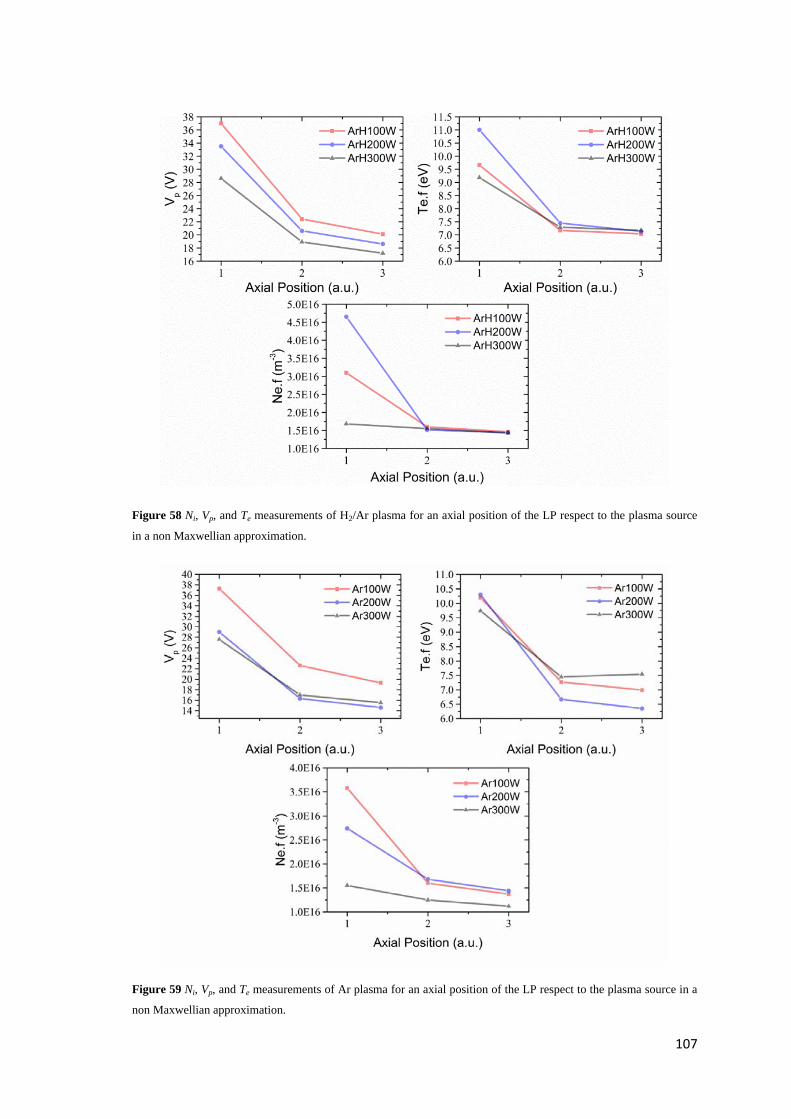
107
Figure 58 Ni, Vp, and Te measurements of H2/Ar plasma for an axial position of the LP respect to the plasma source
in a non Maxwellian approximation.
Figure 59 Ni, Vp, and Te measurements of Ar plasma for an axial position of the LP respect to the plasma source in a
non Maxwellian approximation.

108
6.4 Summary
Taking into account the results from table 12 it is observed that H2/Ar plasma contains the more
energetic ions in comparison with O2/Ar and Ar plasma configurations; in this plasma, the ion
Ar+ has the highest energy in contrast with Ar+ in Ar or O2/Ar plasmas. However, by the
inspection of table 2, one can notice that the lowest cleaning rate is related to H2/Ar plasma
configuration. This indicates that the cleaning rate is not strictly related to the ion kinetic energy
involved in the sputtering process, but rather with chemical interactions involved in the
chemical etching.
In addition by modifying the H2, Ar, and O2 content in the different gas mixtures, it is possible
to increase or reduce the participation of the physical sputtering or chemical erosion, having in
mind that these two processes are required for an efficient carbon cleaning. In the case of H2/Ar,
there should be a right proportion of each one to have the best cleaning rate noticing that the
addition of more hydrogen will improve the chemical etching, while in the case of O2 the
incorporation of Ar will enhance the carbon breaking bonds.
Furthermore, the cleaning rates in H2 and O2 plasmas may also depend on the sp2/sp3
concentration within the carbon contamination. It was found that the neutrals do not play an
important role in the cleaning process as no neutrals were detected having enough kinetic
energy and density to boost the carbon removal from the optics.

109
Chapter 7
7 Plasma Cleaning of Au Reflective Coating
The intention of this chapter is to report on the in-situ cleaning run performed on a test mirror
manufactured using the same materials by the same company that manufactured the M1 optics
from CIRCE beamline. Although the results were not as expected, the procedure that was
carried out and the results will be shown.
7.1 Cleaning the Test Au Mirror (SESO)
7.1.1 Experimental set-up
The cleaning was performed in the chamber described in section 3.1. The plasma characteristic
was the same used for cleaning the EUV filters described in section 5.3.4, in fact, after
observing the good results obtained during and after the plasma cleaning of the Ni, Rh, and Al,
the N2/H2 plasma was selected to clean the contamination on the Au optical coating.
One disk made of aluminum with Ni plating was coated with 55.3nm of Au by THALES SESO
S.A.S, the surface roughness was measured as 8Å rms, and the Au optical coating was done
using electron beam deposition as it done for CIRCE M1 mirror. No chromium binding layer
was added in order to comply with the same characteristics of CIRCE optics.
Following the same carbon coating procedures done in previous experiments (see section 5.2)
the test mirror was contaminated with 80 nm of amorphous carbon (a-C) for simulating a
photon-beam induced carbon contamination. In addition and in order to observe chemical
changes on the surface by using XPS, an Au foil was carbon coated using the same procedure
and cleaned with the same plasma.
The base pressure of the chamber was 4x10⁻⁷mbar (unbaked), the plasma operating pressure was
kept at 0.005 mbar and the feedstock gas used was N2(95%)/H2(5%) supplied via commercial
pre-mix gas bottles (Air Liquide). The RF power of the ICP plasma source was maintained at
100 W. The cleaning time was 10 hours which turned out in a cleaning rate of 1.6Å/min at a
distance of 680mm. Figure 60 shows the evolution of the carbon cleaning.

110
Figure 60 Cleaning evolution of the SESO mirror as a function of time.
In addition to all previous plasma cleaning experiments, an in-situ prototype reflectance set-up
was installed (see Figure 67), in order to check the reduction of the carbon layer thickness
directly on the surface optics.
7.1.2 Results and Discussion
7.1.3 XPS
Figure 61 shows the Au 4f XPS spectrum for plasma-cleaned Au foil using N2/H2 plasma as
compared with the pristine reference Au mono-crystal (111) (i.e., without any treatment). The
binding energy values for the Au foil plasma treated (Au4f, C1s, N1s, and O1s) as obtained
from the plasma treatment are reported in Table 15.
After the cleaning process using N2/H2 plasma, no changes were observed regarding the Au
chemical state which is surprising according to the latter results which shows evidence of gold
cyanidation.

111
Table 15 XPS core level binding energies as obtained from the XPS spectra presented in Figures 61 and 62.
XPS line Reference foil
B. E. (eV)
N2/H2 Plasma
B. E. (eV)
Au 4f 83.66 83.7
87.33 87.37
O1s 531.81 OH-
534.32 Absorbed H2O
C1s 284.49 C-C
285.91 C with N
287.54 Cyanides CN-
289.3 Carbonates
N1s 399.4 CN-
At the first glance, the gold seems not to be chemically affected by the action of the plasma
during the carbon cleaning (see Figure 61). The XPS information does not show any significant
change for the chemical state of gold as was expected according to Cook et al. [67] who found
oxidations state of Au 4f7/2 at a binding energies of (85.6-86 eV) related to AuCN and Au(CN)-2
or as Bas et al. [68] who found oxidation states for Au4f7/2 at a binding energies of (84.7-85.9)
corresponding to Au+ and Au3+.
Figure 61 Left column above, Au4f reference spectrum, below Au 4f after N2/H2 plasma cleaning. Right column,
C1s, and O1s spectrum after plasma treatment.

112
The C1s XPS spectra shows a peak at a binding energy of 287.54 eV attributed to CN- in the
form of AuCN. As shown by the O1s spectra the binding energy of common cyanidation is
531.81 eV which likely originated from OH- in the form of Au(OH)x. In addition to N1s spectra,
the binding energy of cyanidation was found at 399.4eV coming from CN- in the form of
AuCN. All the previous energies for C1s, O1s, and N1s are in good agreement with values
found by Zhong et al. [69].
The fact why no Au oxidation states on gold were found after the plasma treatment could be
attributed to the Au re-passivation process after plasma exposure.
Figure 62 N1s XPS for Au after N2/H2 plasma cleaning
7.1.4 Interference microscopy
The surface roughness of the Au test mirror was analyzed before and after the plasma cleaning
using interferometry microscopy. The instrument used is a phase shifting interferometer
accompanied with a Nikon X10 Mirau interferometric objective (EOTECH Company-
OPTOSURF). The internal reference of the Mirau objective is reconstructed before each
measurement set by averaging 15 measurements on a reference mirror. This reference
topography is then subtracted from all the other measurements done on the samples. Each
topography measurements were done with 5 phase images shifted by π/5.
By the foregoing, the surface roughness was measured in six different zones before the carbon
contamination and subsequent to the plasma cleaning as can be seen in Figure 63. Table 16
collects the roughness values corresponding to each zone in Figure 63.

113
Figure 63 Positions of the measurements for the calculation of the surface roughness from SESO mirror before the
plasma treatment
Table 16 Roughness values corresponding to the zones detailed in figure 63 of the SESO mirror before plasma
cleaning.
Measure
Sample
1
nm rms
nm PV
2
nm rms
nm PV
3
nm rms
nm PV
4
nm rms
nm PV
5
nm rms
nm PV
6
nm rms
nm PV
SESO Au mirror
before plasma
0.667
6.0
0.414
4.8
0.610
6.1
0.435
4.2
0.639
6.5
0.602
14.0
After the plasma cleaning, new surface roughness measurements were performed on the Au test
mirror in a different configuration. This was done taking into account that the mirror was
carbon-coated in the central part (see Figure 60). Figure 64 shows the new configuration where
the measurements were taken. The resulting surface roughness values are shown in table 17.
Figure 64 Positions of the measurements for the calculation of the surface roughness from SESO mirror after the
plasma treatment.

114
Table 17 Roughness values corresponding to the zones detailed in figure 64 of the SESO mirror after plasma cleaning
Measure
Sample
1
nm rms
nm PV
2
nm rms
nm PV
3
nm rms
nm PV
4
nm rms
nm PV
5
nm rms
nm PV
6
nm rms
nm PV
7
nm rms
nm PV
8
nm rms
nm PV
SESO Au mirror
after plasmas
0.522
4.7
0.477
4.3
0.610
6.1
0.565
7.14
0.549
9.4
0.496
5.0
0.530
40.11
0.639
35.6
By comparing the values from Tables 16 and 17, there is apparently a small increase in the
surface roughness of less than 0.1nm rms which is in the range of acceptance. Therefore, at first
glance, the surface roughness as measured with this interference microscopy technique does not
offer evidence for an important change in terms of surface roughness. In addition, when
comparing the results with the values obtained by XPS, we concluded at that time that the
surface neither suffered morphological nor chemical modifications.
Table 18 Average Roughness values corresponding to the zones detailed in figure 64 and detailed in table 17 of the
SESO mirror after plasma cleaning
Average (nm rms)
Before plasma cleaning
Average (nm rms)
After plasma cleaning
Average (nm rms)
After plasma cleaning on
the outer diameter
Average (nm rms)
After plasma cleaning
on former carbon spot
6 measurements
0.561
8 measurements
0.549
4 measurements
0.568
4 measurements
0.500
7.1.5 Results from XRR measurements
By using XRR the thickness and roughness of the SESO mirror were measured. By using this
technique, the obtained data resulted in a completely different picture with respect to the
previous interference microscopy technique.
The Au thickness after plasma treatments was determined as 42 nm which implies a reduction in
Au thickness of 13.3 nm while the Au-Roughness was measured to be between 1.4-1.6nm rms
which indicate an increase of the double in surface roughness compared to the original value of
8Å rms and three times larger than values obtained from the interferometer microscope.
The significant drawbacks from the N2/H2 plasma cleaning become most apparent from the
XRR measurements presented in Figure 65. It is clearly seen that Au is not uniform across the
center of the mirror in comparison with the edges; this could indicate a lower damage in the

115
zone where the carbon was deposited. This detrimental effect could be possible due to the
formation of the cyanide coming from the ammonia reacting with the carbon on the optics
surface.
Figure 65 XRR data from the Au-coated test mirror after cleaning with N2/H2 plasma (red solid lines: experimental
XRR data; black solid lines: IMD simulation). A and B correspond to the mirror off-center areas where no C was
deposited, while C is the measurement on the central part of the mirror after a-C coating and subsequent N2/H2
plasma cleaning.
7.1.6 Gas Analysis (RGA)
By using the differentially pumped RGA within the experimental setup, we obtained similar
results that in the case of the EUV filters (see chapter 5.3.5), thus confirming the formation of
NH3 within the N2/H2 plasma. Figure 66 shows the RGA time trend from that N2/H2 plasma
cleaning process of the Au SESO mirror. In contrast to the N2/H2 plasma cleaning of the EUV
filters, on this run, the formation of hydrogen cyanide (CNH, mass 27 a.u.) was observed. This
reaction can be promoted by the interaction of hydrogen, carbon and nitrogen compounds given
by equation 19 as already discussed in chapter 5.3.5.
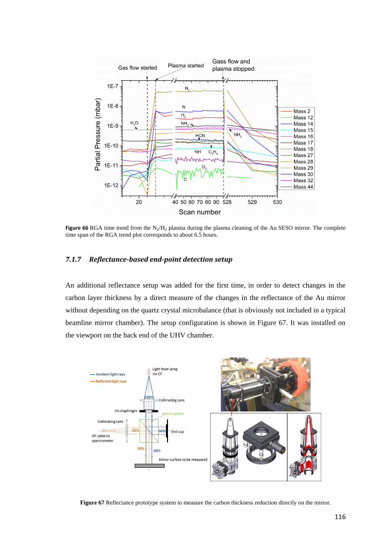
116
Figure 66 RGA time trend from the N2/H2 plasma during the plasma cleaning of the Au SESO mirror. The complete
time span of the RGA trend plot corresponds to about 6.5 hours.
7.1.7 Reflectance-based end-point detection setup
An additional reflectance setup was added for the first time, in order to detect changes in the
carbon layer thickness by a direct measure of the changes in the reflectance of the Au mirror
without depending on the quartz crystal microbalance (that is obviously not included in a typical
beamline mirror chamber). The setup configuration is shown in Figure 67. It was installed on
the viewport on the back end of the UHV chamber.
Figure 67 Reflectance prototype system to measure the carbon thickness reduction directly on the mirror.

117
The reflectance setup consists of two collimators connected through a beam-splitter and one iris
which allow modifying the size of the beam. The light used comes from a halogen lamp model
HL-2000 Family from Ocean Optics with a wave range of 360-2400nm. The collimator (model
84-UV-25 collimating lens) permits collimating light at long distances up to 12 meters. The
system was connected via an optical fiber to a spectrometer.
Figure 68 Normalized reflection data as measured with the setup shown in Figure 67 before, during, and after plasma
cleaning of the Au test mirror.
The normalized reflection collected by using this setup can be seen in Figure 68. As can be
seen, there is a reduction in the reflection spectra of the Au after the plasma cleaning. At the
beginning we assumed this intensity decreasing in the reflection due to alignment issues. But
certainly, the reduction in reflection may correspond to the increase in the Au roughness.
The gold thickness reduction rate was estimated to be 0.32Å/min after the 10 hours of plasma
cleaning at a distance of 680mm.

118

119
Conclusions
Plasmas - due to their rich plasma chemistry and their capability of producing a large amount of
stable species, is presented as a viable alternative to be taken into account in order to condition
different optical components suffering from carbon contaminations. Among the different
plasmas being available, inductively coupled plasma (ICP) arise as a promising alternative due
to their specific configuration since this kind of plasma is highly non-invasive – i.e., does not
require electrodes to its ignition as the CCP – and can be operated in a remote manner, which
ensures low ion kinetics within that could be harmful for the coatings, especially due to its
remote operation and “plasma afterglow” characteristics.
It was found that by having specific configurations in terms of feedstock gas mixture, RF
power, operating pressures and cleaning time, different optical components subject to specific
conditions such as oxidizing coatings, ultra-high vacuum, and complex carbon-containing
optical coatings can be cleaned via ICP. Nonetheless, it was realized that the cleaning process
involved in the different plasma configurations are complex within themselves and different
with respect to each other. In that sense, during the plasma cleaning molecular gases can be
activated by dissociation which will induce physical sputtering, chemical cleaning or a mixture
of these two sub-processes. In addition, contributions from the UV light as well as other plasma
emission wavelength coming from metastable ions have to be considered as an additional active
component in the cleaning process.
In accordance to the aforesaid, the need of various plasma diagnostics is demonstrated to
understand how the species produced in the plasma do interact - not only with carbon
contaminations layers, but also with the optical coatings themselves. Based on this, the selection
of a specific plasma configuration for the cleaning a specific optical coating can be performed.
Based on our analysis regarding the remote ICP plasma used, we conclude that the pure O2
feedstock gas yields excellent results regarding both the a-C cleaning as well as the preservation
of B4C optical coatings.
A favorable combination of a N2(95%)/H2(5%) plasma feedstock gas mixture leads to the best
chemical surface preservation and cleaning results for non-inert metal optical coatings such as
Ni, Rh, and Al together with the removal of carbon contaminations and including an acceptable
carbon cleaning rate.

120
However, the same N2/H2 gas mixture or any gas mixture simultaneously containing nitrogen
and hydrogen, turn out to be detrimental for optical coatings such as Au, Ag, and Cu. This could
be confirmed after the plasma cleaning on the Au SESO mirror which suffered of an increase in
roughness surface in almost the double in comparison to the original value. This increasing in
the Au roughness was produce by the oxidation triggered by the cyanides. The cyanides are a
secondary reaction which comes from the interaction of the ammonia and the carbon
contamination.
Thus, the use of specific gas mixtures for low-pressure RF plasma is to be carefully considered
and tested prior to any cleaning on real beamline optical components in the field.
Last but not least, a first efficient ex-situ carbon cleaning of Al EUV filters used at the FERMI
FEL1 as a concrete application of N2/H2 plasma could be demonstrated.

121
Bibliography
[1] M. Gonzalez, J. Reyes,I. Šics, A.R. Goñi, H. Moreno, V. Carlino, and E. Pellegrin. Remote
plasma cleaning of optical surfaces: Cleaning rates of different carbon allotropes as a function
of RF powers and distances. Applied Surface Science 362 (2016) 448-458.
[2] E. Pellegrin, I. Šics, J. Reyes, C. Perez, J. Lopez, M. Langlois, J. Fernandez and V. Carlino.
Characterization, optimization and surface physics aspects of in situ plasma mirror cleaning. J.
Synchrotron Rad. 21 (2014) 300-314.
[3] S. Graham, C. Steinhaus, M. Clift, and L. Klebanoff. Radio-frequency discharge cleaning of
silicon-capped Mo/Si multilayer extreme ultraviolet optics, J. Vac. where the latter are used as
carbon sources for the thin film deposition. Sci. Technol. B 20 (2002) 2393.
[4] A. Thedsakhulwong and W. Thowladda. Removal of carbon contamination on silicon wafer
surfaces by microwave oxygen plasma. J. Metals Mater. Miner. 18 (2008) 137–141.
[5] E. Strein, D. Allred, M.R. Linford. Use of a commercial RF plasma cleaner in eliminating
adventitious carbon contamination in an XPS system. Microsc. Microanal. 14 (2008) 818–819.
[6] F. Eggenstein, F. Senf, T. Zeschke, and W. Gudat. Cleaning of contaminated XUV-optics at
BESSY II. Nucl. Instrum. Methods Phys. Res. A 325 (2001) 467–468.
[7] C. Hopf, A. von Keudell and W. Jacob. Chemical sputtering of hydrocarbons films by low-
energy Ar+ ion and H atom impact. Nucl. Fusion 42 (2002) L27-L30.
[8] F. O. Minotti. Apuntes de Física del Plasma. http://www.lfp.uba.ar/es/notas.php. 2005
(accessed February 1 2018 )
[9] K. Wiesemann. A short introduction to plasma physics. AEPT, Ruhr-Universität Bochum,
Germany (2014).
[10] Alexander Friedman. Plasma Chemistry. Cambridge University press (2008).
[11] Thierry. Plasma science and technology. http://www.thierry-corp.com/plasma (acceded
January 20 2018).
[12] A. M. Lieberman and A.J. Lichtenberg. Principles of plasma discharges and materials
processing. Published by John Wiley & Sons, Inc. (2005).
[13] Tomohiro Okumura. Inductively coupled plasma sources and applications. Physics
Research International (2010) doi:10.1155/2010/164249.
[14] K. Burm. Breakdown magnetic field in an inductively coupled plasma. Physics Letters A
372 (2008) 6280-6283.
[15] D. Attwood. X-rays and extreme ultraviolet radiation, principles and applications.
Published by the press syndicate of the University of Cambridge (2000).
[16] H. Winick. Fourth generation light sources. Stanford, CA 94309, USA (1998) 37-41.
[17] A. Gutiérrez, J. A. Martín, S. Ferrer. La luz sincrotrón: una herramienta extraordinaria
para la ciencia. Apuntes de Ciencia y Tecnología 12 (2004) 37-46.

122
[18] J. Feldhaus, J. Arthur and J. B. Hastings. X-ray free electron lasers. J. Phys. B: At, Mol.
Op. Phys. 38 (2005) S799-S819.
[19] W. J. Brian and N. R. Thompson. X-ray free electron lasers. Nature Photonics 4 (2010)
814-821.
[20] E. Pellegrin. et al. RF plasma cleaning of mirror surfaces: Characterization, optimization,
and surface physics aspects of plasma cleaning. Published in Proceedings of SPIE - The
International Society for Optical Engineering 8777 (2013).
[21] J. Benedikt, A. Hecimovic, D. Ellerweg, and A. Keudell. Quadrupole mass spectrometry of
reactive plasmas. J. Phys. D: Appl. Phys. 45 (2012) 403001.
[22] J. Perrin. Plasma Processing of Semiconductors ed PFW Williams (Dordrecht: Kluwer)
(1997) 397–432.
[23] R.L. Merlino. Understanding Langmuir probe current-voltage characteristics. Am. J.
Phys. 75-12 (2007) 1078-1085.
[24] F. Chen. Langmuir probes in RF plasma: surprising validity of OML theory. Plasma
Sources Sci. Technol. 18 (2009) 035012.
[25] F. Chen and J. P. Chang. Lectures on principles of plasma processing. Plenum/Kluwer
Publishers 2002.
[26] A. C. Ferrari and J. Robertson, Interpretation of Raman spectra of disordered and
amorphous carbon, Physical Review B 61-20 (2000) 14095-14107.
[27] H. Moreno, S. Hussain, R. Amade and E. Bertran. Growth and functionalization of CNTs
on stainless steel electrodes for supercapacitor applications. Materials research express 1
(2014) 035050.
[28] J. F. Moulder, W. F. Stickle, P. E. Sobol and K. D. Bomben. Handbook of X-ray
photoelectron spectroscopy. Published by Physical Electronics, Inc. U.S.A. 1995.
[29] D.L. Windt. IMD-Software for modeling the optical properties of multilayer films. Comput.
Phys. 12 (1998) 360.
[30] V. Domnich., S. Reynaud, R.A. Haber and M. Chhowalla. Boron carbide: Structure,
properties, and stability under stress. J. Am. Ceram. Soc. 94 (2011) 3605–3628.
[31] M. Stoermer, F. Siewert, and H. Sinn. Preparation and characterization of B4C coatings
for advanced research light sources. J. Synchrotron Radiat. 23 (2016) 50-58.
[32] B. Mertens et al. EUV time-resolved studies on carbon growth and cleaning. in (ed.
Engelstad, R. L.) 95 (2003). doi:10.1117/12.504542.
[33] K. Boller, R.P. Haelbich, H. Hogrefe, W. Jark, and C. Kunz. Investigation of carbon
contamination of mirror surfaces exposed to synchrotron radiation. Nucl. Instruments Methods
Phys. Res. 208 (1983) 273–279.
[34] T. Koide et al. Investigation of carbon contamination of synchrotron radiation mirrors.
Nucl. Instruments Methods. 246 (1986) 215–218.
[35] P. Fernandez and R. Barrett. Recovery strategies for mirrors with boron carbide-based

123
coatings for 6. x nm lithography. private communication. (2012).
[36] L. G. Jacobsohn, R.K. Schulze, M.E.H. Maia Da Costa, and M. Nastasi. X-ray
photoelectron spectroscopy investigation of boron carbide films deposited by sputtering. Surf.
Sci. 572 (2004) 418–424.
[37] S. Jacques et al. LPCVD and characterization of boron-containing pyrocarbon materials.
Carbon 34 (1996) 1135–1143.
[38] S. Li et al. Effects of heat treatment on the microstructure of amorphous boron carbide
coating deposited on graphite substrates by chemical vapor deposition. Thin Solid Films 519
(2010) 251–258.
[39] H. Moreno, D. Rogler, G. Sauthier, M. Thomasset, R. Dietsch, V. Carlino, E. Pellegrin.
Characterization of carbon-contaminated B4C-coated optics after chemically selective cleaning
with low-pressure RF plasma. Scientific Reports 8 (2018) 1293.
[40] E. Allaria et al., Highly coherent and stable pulses from the FERMI seeded free-electron
laser in the extreme ultraviolet. Nature Photonics 6 (2012) 699-704.
[41] X-Ray Photoelectron Spectroscopy (XPS) Reference Pages. http http://www.xpsfitting.com/
search/label/Nickel 2015 (accessed 19 December 2017).
[42] M. C. Biesinger, L.W. Lau, A. R. Gerson and R.St. C. Smart. The role of the Auger
parameter in XPS studies of nickel metal, halides and oxides. Phys. Chem. Chem. Phys. 14
(2012) 2434-2442.
[43] L. Kibis, A. Stadnichenko, S. Koscheev, V. Zaikovskii and A. Boronin. XPS of
nanostructured Rhodium oxide film comprising Rh4+ species. J. Phys Chem. C 120 (2016)
19142-19150. (revisar ref desde aqui)
[44] X-Ray Photoelectron Spectroscopy (XPS) Reference Pages
http://www.xpsfitting.com/search/
label/Rhodium 2015 (accessed 19 December 2017).
[45] A. Tolia, R. Smiley, W. Delgass, C. Takudis and M. Weaver. Surface oxidation of
Rhodium at ambient pressures as probed by surface-enhanced Raman and X-Ray photoelectron
spectroscopies. Journal of Catalysis 150 (1994) 56-70.
[46] Thermo scientific XPS https://xpssimplified.com/elements/aluminum.php 2013 (accessed
19 December 2017).
[47]I. Latsunskyi, M. Kempinski, M. Jancelewicz, K. Zaleski, S. Jurga, and V. Smyntyna.
Structural and XPS characterization of ALD Al2O3 coated porous silicon. Vacuum 113 (2015)
52-58.
[48] J. Zähr, S. Oswald, M. Türpe, H.J. Ullrich and U. Füssel. Characterization of oxide and
hydroxide layers on technical aluminum materials using XPS. Vacuum 86 (2012) 1216.
[49] B. R. Strohmeier. An ESCA Method for determining the oxide thickness on aluminum
alloys. Surface and interface analysis 15 (1990) 51-56.

124
[50] E. Carrasco, M. Jiménez, I. Tanarro and V. Herrero. Neutral and ion chemistry in low-
pressure dc plasmas of H2/N2 mixtures: routes for the efficient production of NH3 and NH4+.
Phys. Chem. Chem. Phys. 13 (2011) 19561-19572.
[51] L.C. Ciobotaru and I. Gruia. Study of the carbon atoms production in methanol/ethanol-
nitrogen flowing post-discharge plasma. Rom. Journ. Phys. 60 (2015) 1536-1549.
[52] H.W, Leutner. Production of hydrogen cyanide using a plasma jet. Ind. Eng. Chem.
Process Des. and Dev. 2(4) (1963) 315-318.
[53] A. Merenda, E. Ligneris, K. Sears, T. Chaffraix, K. Magniez, D. Cornu, J. Schütz and L.
Dumée. Assessing the temporal stability of surface functional groups introduced by plasma
treatments on outer shells of carbon nanotubes. Scientific Reports 6 (2016) 31565.
[54] A. Brockhaus, C. Borchardt and J. Engemann. Langmuir probe measurements in
commercial plasma plants. Plasma Sources Sci. Technol. 3 (1994) 539.
[55] A. Brockhaus, D. Korzec, F. Werner, Y. Yuan, and J. Engemann. Characterization of a
microwave plasma by in situ diagnostics. Surface and Coating Technology 74-75 (1995) 431-
442.
[56] C. Roth, G. Oberbossel, and R.P. Von Rohr. Electron temperature, ion density and energy
influx measurements in a tubular plasma reactor for powder surface modification. Journal of
Physics D: Applied Physics 45-35 (2012) 355202.
[57] J. T. Gudmundsson. Ion energy distribution in H2/Ar plasma in a planar inductive
discharge. Plasma Sources Sci. Technol. 8 (1999) 58-64.
[58] J. Benedikt, A. Hecimovic, D. Ellerweg and A. Keudell. Quadrupole mass spectrometry of
reactive plasmas. J. Phys. D: Appl. Phys. 45 (2012) 403001.
[59] A. Mishra, T. Hyung, K. Nam and G. Young. Mass spectrometric study of discharges
produced by a large-area dual-frequency dual-antenna inductively coupled plasma source. J.
Phys. D: Appl. Phys. 45 (2012) 475201.
[60] R. Hippler, J. Kredl and V. Vartolomei. Ion energy distribution of an inductively couple
radiofrequency discharge in argon and oxygen. Vacuum 83 (2008) 732-737.
[61] C. Hayden, D. Gahan and M. Hopkins. Ion energy distributions at capacitively and directly
couple electrode immersed in a plasma generated by a remote source. Plasma Sources Science
and Technology 18 (2009) 025018.
[62] M. Sode, T. Schwartz and W. Jacob. Ion chemistry in H2-Ar low temperatures plasmas.
Journal of Applied Physics 114 (2013) 063302.
[63] W. Liu, D. Wen, S.Zhao, F. Gao and Y. Wang. Characterization of O2/Ar inductively
couple plasma studied by using a Langmuir probe and global model. Plasma Sources Sci.
Technol. 24 (2015) 025035.
[64] K. Takechi and M.A. Lieberman. Effect of Ar addition to an O2 plasma in an inductively
coupled, traveling wave driven, large area plasma source: O2/Ar mixture plasma modeling and
photoresist etching. J. Apply. Phys. 90(7) (2001) 3205-3211.

125
[65] M Schulze, A Yanguas-Gil, A von Keudell and P Awakowicz. A robust method to measure
metastable and resonant state densities from emission spectra in argon and argon-diluted low
pressure plasmas. J. Phys. D: Appl. Phys. 41 (2008) 065206.
[66] D. A. Hook, J. A. Ohlhausen, J. Krim, and M. T. Dugger. Evaluation of Oxygen Plasma
and UV Ozone Methods for Cleaning of Occluded Areas in MEMS Devices. Journal of
Microelectromechanical Systems 19-6 (2010) 1292-1298.
[67] R. Cook, E.A. Crathorne, A.J. Monhemius and D.L. Perry. An XPS study of the adsorption
f gold (I) cyanide by carbons. Hydrometallurgy 22 (1989) 171-182.
[68] A. Deniz, F. SAFIZADEH, W. ZHANG, E. GHALI, Y. CHOI. Active and passive
behaviors of gold in cyanide solutions. Trans. Nonferrous Met. Soc. China 25(2015)
3442−3453.
[69] Q. Zhong, Y. Yang, L. Chen, Q. Li, B. Xu and T. Jiang. Intensification behavior of
mercury ions on gold cyanide leaching. Metals 8 (80) (2018).

126

127
Table of Figures
Figure 1 ICP geometries. Cylindrical A, planar B, half-toroidal C. ............................................ 16
Figure 2 Breakdown magnetic field of the GV10x for different feedstock gases. ...................... 18
Figure 3 Basic scheme of the GV10x plasma tube for calculating the approximately generated
magnetic field .............................................................................................................................. 19
Figure 4 Typical Storage ring in a synchrotron. Electrons are accelerated in a linear accelerator
(LINAC) passing to a circular booster accelerator inside the storage ring. Subsequently, the
electrons are injected into the storage ring where bending magnets are installed to bend the
electron trajectories. Quadrupole and sextupole magnets focus and correct the electron beam. 21
Figure 5 Agular radiation distribution emitted by a charged particle in a circular motion, where
a is the centripetal acceleration. For small velocities there is no emission in the direction parallel
to the acceleration, classical case A. In the relativistic case, for velocities near the speed of light,
the distribution produces a cone tangential to the particle trajectory. ......................................... 22
Figure 6 Brilliance of x-ray sources: A historical graph showing the increase in terms of
brilliance, left column. Typical spectral brilliance curves of magnetic insertion devices used in
third generation synchrotrons, center column. Undulator and bending magnet schemes, right
column. Images are taken from http://wiley-vch.e-bookshelf.de/products/reading-epub/product-
id/596420 (January 29, 2018) ..................................................................................................... 24
Figure 7 Some geometrical configurations for synchrotron mirrors. On top, a toroidal mirror
image courtesy of N. Roman from ALBA synchrotron. In the center, a W/B4C mirror, image
was taken from http://www.ntt-at.com/product/multilayer/ (January 29, 2018). Bottom row, an
ellipsoidal mirror, image was taken from http://www.ntt-at.com/product/multilayer/. (January
29, 2018).and an Al parabolic mirror, image was taken from http://mbdaps.com/precision-
optical/parabolicmirrors.htm (January 29, 2018) ........................................................................ 27
Figure 8 Schematical description of the plasma cleaning chamber (QCM: Quartz crystal
monitor; RGA: Residual gas analyzer; S.M.: Sample manipulator) ........................................... 31
Figure 9 A: QMS scheme, B: Schematic representation of electrostatic energy analyzer (ESA).
..................................................................................................................................................... 35
Figure 10 Two distinct features for high-frequency sheaths in H2/A2 plasma produced by the
GV10x at 100W. Red line shows the IEDF behavior for ion transit times longer than the RF
period. The black line shows the IEDF for ion transit time shorter than the RF period. ............ 37
Figure 11 Electrical connection of a cylindrical QMS. ............................................................... 38
Figure 12 Typical standard EQP system. Image taken from EQP/EQS Analyzer operator´s
Manual of Hiden Analytical Limited. p. 8. (February 2, 2018) .................................................. 39
Figure 13 I-V curve from the ICP GV10x in and AR plasma discharge .................................... 41
Figure 14 Raman spectra from different carbon contaminations. Red solid line: Carbon footprint
on EUV Al filter foil upstream side; Black solid line: a-C thin film from e-beam carbon
deposition; Blue solid line: Carbon footprint on EUV Al filter foil downstream side; green solid
line: Carbon footprint an Au-coated from SRC soft X-ray beamline. ........................................ 44
Figure 15 Photoemission process involved in XPS. A. an incoming photon causes the emission
of a photoelectron. B. the relaxation process resulting in the emission of a KL23L23 electron
(Auger electron). ......................................................................................................................... 47

128
Figure 16 Left column: Si(100) test wafers (10x10 mm2 size) provided with a B4C coating stripe
(ochre color – see left-hand side panel) plus a central amorphous carbon contamination spot
(dark grey color – see right-hand side panel) on top of the B4C layer. Right column: Optically
polished Si test mirrors with one-inch diameter. The mirror on top shows a pristine B4C coating,
while the mirror in the lower part exhibits one half of its surface (i.e., the darker part) coated
with an additional amorphous carbon layer with 70 nm thickness. ............................................ 54
Figure 17 B4C-coated Si test wafers and test mirrors before (left) and after (right) O2/Ar plasma
cleaning ....................................................................................................................................... 55
Figure 18 High-resolution C1s and B1s XPS spectra of the B4C-coated test wafer before (black
solid lines) and after O2/Ar RF plasma cleaning (red solid lines). Left panel: XPS data taken on
the amorphous carbon contamination spot. Right panel: XPS data taken off the amorphous
carbon contamination spot on the bare B4C coating. .................................................................. 56
Figure 19 XPS survey scans taken from B4C-coated Si test wafers before (solid black lines) and
after (solid red lines) O2/Ar plasma cleaning. The left and right-hand side diagram shows the
XPS spectra taken at a sample location on and off the amorphous carbon spot, respectively .... 57
Figure 20 XPS high resolution scans taken from a B4C-coated Si test wafer after the O2/Ar
plasma cleaning. The left and right-hand side diagram show the B1s and the C1s XPS spectra
taken at a sample spot corresponding to the location of the amorphous carbon spot. ................ 58
Figure 21 XRR data from B4C-coated test mirror right after O2/Ar plasma cleaning. A pristine
B4C-coated Si test wafer right after B4C deposition, B after 7 months of storage in air C: Non-a-
C coated part; D: Formerly a-C coated part (red solid lines: experimental XRR data; black solid
lines: IMD simulation). ............................................................................................................... 59
Figure 22 Comparison of XRR total reflection data at low grazing angles for a pristine B4C-
coated test mirror (black line) and after a-C coating plus subsequent O2/Ar plasma cleaning
(green line: formerly a-C coated area; red line: non a-C coated area). ....................................... 60
Figure 23 SEM images of B4C-coated test wafers taken at 20 kV electron acceleration voltage
with a 250k-fold magnification: A Pristine B4C-coated test wafer, B O2/Ar-plasma cleaned –
formerly a-C coated part, and C O2/Ar-plasma cleaned – non a-C coated part. ......................... 61
Figure 24 B4C-coated Si test mirrors during various stages of the process. Left: Pristine B4C-
coated Si mirror; Center: Mirror after a-C coating (full mirror surface coated); Right: Mirror
after cleaning with pure O2 plasma. ............................................................................................ 62
Figure 25 High-resolution C1s and B1s XPS spectra of the B4C-coated test wafer before (black
solid lines) and after H2/Ar RF plasma cleaning (red solid lines). Left panel: XPS data taken on
the amorphous carbon contamination spot. Right panel: XPS data taken off the amorphous
carbon contamination spot on the bare B4C coating. .................................................................. 63
Figure 26 XPS survey scans taken from B4C-coated Si test wafers before (solid black lines) and
after (solid red lines) H2/Ar plasma cleaning. The left and right-hand side diagram show the
XPS spectra taken at a sample location on and off the amorphous carbon spot, respectively. ... 63
Figure 27 A, B XPS high resolution scans taken from B4C-coated Si test wafers after the 10
minutes of Ar sputtering (at 0.5 keV) performed in the XPS analysis chamber. C and D
diagrams show the B1s and the C1s XPS spectra taken after the H2/Ar plasma cleaning. ......... 64
Figure 28 XRR data from B4C-coated test mirror right after H2/Ar plasma cleaning. Left-hand
side: Non-a-C coated part; right-hand side: Formerly a-C coated part (red solid lines:
experimental XRR data; black solid lines: IMD simulation). ..................................................... 65

129
Figure 29 Comparison of XRR total reflection data at low grazing angles for a pristine B4C-
coated test mirror (black line) and after a-C coating plus subsequent H2/Ar plasma cleaning
(green line: formerly a-C coated area; red line: non a-C coated area). ....................................... 66
Figure 30 SEM images of B4C-coated test wafers taken at 20 kV electron acceleration voltage
with a 250k-fold magnification after cleaning with H2/Ar plasma: A Formerly a-C coated part,
and B non a-C coated part. .......................................................................................................... 67
Figure 31 B4C-coated Si test mirrors during various stages of the process. Left: Pristine B4C-
coated Si mirror; Center: Mirror after a-C coating (full mirror surface coated); Right: Mirror
after cleaning with pure O2 plasma. ............................................................................................ 67
Figure 32 High-resolution C1s and B1s XPS spectra of the B4C-coated test wafer before (black
solid lines) and after pure O2 RF plasma cleaning (red solid lines). Left panel: XPS data taken
on the amorphous carbon contamination spot. Right panel: XPS data taken off the amorphous
carbon contamination spot on the bare B4C coating ................................................................... 68
Figure 33 XPS survey scans taken from B4C-coated Si test wafers before (solid black lines) and
after (solid red lines) pure O2 plasma cleaning. The left and right-hand side diagram show the
XPS spectra taken at a sample location on and off the amorphous carbon spot, respectively. ... 69
Figure 34 XRR data from B4C-coated test mirror after cleaning with pure O2 plasma cleaning.
(red solid lines: experimental XRR data; black solid lines: IMD simulation). ........................... 69
Figure 35 Comparison of XRR total reflection data for a pristine B4C-coated test mirror (black
line), after a-C. Coating (red line), and after subsequent cleaning with pure O2 plasma (green
line). ............................................................................................................................................ 70
Figure 36 SEM images of B4C-coated test wafers taken at 20 kV electron acceleration voltage
with a 250k-fold magnification after cleaning with pure O2 plasma: A Formerly a-C coated part,
and B non a-C coated part. .......................................................................................................... 72
Figure 37 Ni, Rh, Al, and Au metal foils of micrometric thickness installed on a common foil
sample holder for plasma treatment. Left: Metal foil sample holder before plasma cleaning,
including a 50 nm a-C coating. Right: Metal foil sample holder after plasma cleaning. ............ 79
Figure 38 Ni 2p (left column) and O 1s (right column) XPS core level spectra of Ni metal foils.
Bottom row: Pristine Ni reference sample; Center row: Ni foil after a-C contamination and
subsequent N2/O2/H2 plasma treatment; Top row: Ni foil after a-C contamination and
subsequent N2/H2 plasma treatment ............................................................................................ 80
Figure 39 Rh 3d (left column) and O 1s (left column) XPS core level spectra of Rh metal foils.
Bottom row: Pristine Rh metal reference sample; Center row: Rh foil after a-C contamination
and subsequent N2/O2/H2 plasma treatment; Top row: Rh foil after a-C contamination and
subsequent N2/H2 plasma treatment. ........................................................................................... 82
Figure 40 Al 2p (left column) and O 1s (right column) XPS core level spectra of Al metal foils.
Bottom row: Pristine Al reference sample; top row: Al foil after a-C contamination and
subsequent N2/H2 plasma treatment. ........................................................................................... 83
Figure 41 A. Upstream side of a self-sustained Al filter foil with 100 nm thickness used at the
FERMI FEL1. The foil wrinkles within the carbon footprint induced by the deposition of the
carbon layer at elevated foil temperatures can be clearly distinguished. B. The upstream side of
four different self-sustained Al filter foils with 100 nm foil thickness used at the FERMI FEL1
before (left column) and after (right column) N2/H2 plasma treatment. Several photon beam-
induced carbon footprints per each filter foil can clearly be distinguished from the images in the
left-hand side column .................................................................................................................. 85
130
Figure 42 RGA time trend from the N2/H2 plasma during the plasma cleaning of the EUV Al
foil filters. The complete time span of the RGA trend plot corresponds to about 4 hours and 50
minutes. ....................................................................................................................................... 86
Figure 43 C1s for the different materials after the carbon contamination and subsequent plasma
cleaning. Left column Rh as reference sample, after N2/O2/H2 plasma (center) and after N2/H2
plasma (bottom). Center column Ni and right column Al as reference material and after N2/H2
plasma. ........................................................................................................................................ 87
Figure 44 N1s XPS for Rh, Ni, and Al materials after N2/H2 plasma cleaning. ......................... 87
Figure 45 Plasma diagnosis chamber. ......................................................................................... 92
Figure 46 Plasma gradient distribution inside the chamber. ....................................................... 93
Figure 47 Double-probe current-voltage characteristics for an Ar plasma at 300 W RF power at
d1 axial position. ......................................................................................................................... 95
Figure 48 IEDs for H3+, H2
+, H+, Ar+ and ArH+ in a H2/Ar plasma at different RF powers and
two MS to source distances. At the top left the corresponding mass scan can be seen. ............. 97
Figure 49 IEDs for O2+, O+, and Ar+ in O2/Ar plasma at different RF powers and two distances.
At the top left the corresponding mass scan is shown. ................................................................ 98
Figure 50 Plasma potential gradients in the axial direction as a function of the plasma source
distance as determined by a Maxwellian approximation obtained from values measured using
the LP for the three different plasma. .......................................................................................... 99
Figure 51 Ion density gradients in the axial direction as a function of the plasma source distance
obtained from values measured using the LP for the three different plasmas. ......................... 100
Figure 52 IEDF for Ar+ in Ar plasma at different RF power and one distance. On the left the
corresponding mass scan. .......................................................................................................... 100
Figure 53 Density variations of the 3p54p levels for RF power at 100, 200 and 300 W ........... 103
Figure 54 Plasma potential behavior regarding to the ion density calculated by using the OML
theory for the three plasma configurations in an axial configuration. ....................................... 104
Figure 55 Plasma potential regarding the electron temperature calculated by using the second
derivative of the I-V. ................................................................................................................. 105
Figure 56 Ni, Vp, and Te measurements for a radial position of the LP respect to the plasma
source. ....................................................................................................................................... 105
Figure 57 Ni, Vp, and Te measurements of O2/Ar plasma for an axial position of the LP respect to
the plasma source in a non Maxwellian approximation. ........................................................... 106
Figure 58 Ni, Vp, and Te measurements of H2/Ar plasma for an axial position of the LP respect to
the plasma source in a non Maxwellian approximation. ........................................................... 107
Figure 59 Ni, Vp, and Te measurements of Ar plasma for an axial position of the LP respect to
the plasma source in a non Maxwellian approximation. ........................................................... 107
Figure 60 Cleaning evolution of the SESO mirror as a function of time. ................................. 110
Figure 61 Left column above, Au4f reference spectrum, below Au 4f after N2/H2 plasma
cleaning. Right column, C1s, and O1s spectrum after plasma treatment. ................................. 111
Figure 62 N1s XPS for Au after N2/H2 plasma cleaning .......................................................... 112
Figure 63 Positions of the measurements for the calculation of the surface roughness from SESO
mirror before the plasma treatment ........................................................................................... 113
Figure 64 Positions of the measurements for the calculation of the surface roughness from SESO
mirror after the plasma treatment. ............................................................................................. 113

131
Figure 65 XRR data from the Au-coated test mirror after cleaning with N2/H2 plasma (red solid
lines: experimental XRR data; black solid lines: IMD simulation). A and B correspond to the
mirror off-center areas where no C was deposited, while C is the measurement on the central
part of the mirror after a-C coating and subsequent N2/H2 plasma cleaning. ............................ 115
Figure 66 RGA time trend from the N2/H2 plasma during the plasma cleaning of the Au SESO
mirror. The complete time span of the RGA trend plot corresponds to about 6.5 hours. ......... 116
Figure 67 Reflectance prototype system to measure the carbon thickness reduction directly on
the mirror................................................................................................................................... 116
Figure 68 Normalized reflection data as measured with the setup shown in Figure 67 before,
during, and after plasma cleaning of the Au test mirror. ........................................................... 117