Advancements in Thermal Management at PCB … · for Electronics Design and Fabrication Presented...
76
Advancements in Thermal Management at PCB Level for Electronics Design and Fabrication Presented By: Pratish Patel Electronic Interconnect www.eiconnect.com [email protected] 1
Transcript of Advancements in Thermal Management at PCB … · for Electronics Design and Fabrication Presented...

Advancements in Thermal
Management at PCB Level
for Electronics Design and
Fabrication
Presented By:
Pratish Patel
Electronic Interconnect
www.eiconnect.com
1

Table of Content
Challenges of the Electronics
CFD Analysis under Natural Convection
between FR4 and MCPCB.
Design Guidelines
Fabrication Guidelines
Question and Comments.
2

Challenges of the Electronics
The electronics Industry today is facing challenges such as
HOT SPOT
CTE mismatch,
solder joint stress,
thermal fatigue failure
shock and vibration issues,
“SMALLER, FASTER, STRONGER”
3

Challenges of the Thermal Management
Improve thermal performance for reduced junction temps
Heat sink design with optimized performance to weight ratios
Increase color quality and light output
Increase product lifespan
Increase energy efficiency
Save material cost by optimizing material usage
Decrease UL failures with better designs the first time
Eliminate color shift
4

A comparative study between
FR4 and other PCB’s using
CFD Analysis under Natural
Convection.
Case Study
5 5

To conduct a comparative study between FR4 and other
PCB’s using CFD Analysis under Natural Convection.
Four separate boards (FR4, Laird’s Metal clad1KA) with
different thermal conductivities were modeled.
Two different heat sources were provided to each LED (0.06
W & 0.2 W).
48 LED’s were populated on each PCB.
Two heat sink designs were proposed for each LED wattage
type (0.06 W & 0.2 W).
The ambient temperature for each model was 250 C.
OBJECTIVE
6

Thermal Model Layout
Simplified Thermal Model
Thermal Analysis 1:
- Four different PCB’s (LED = 0.06 W)
Thermal Analysis 2:
- Heat Sink Design for eight PCB’s (LED = 0.06 W)
Thermal Analysis 3:
- Four different PCB’s (LED = 0. 2 W)
Thermal Analysis 4: - Heat Sink Design for Four PCB’s (LED = 0.2 W)
Results & Conclusion 7
OUTLINE

Thermal Model Layout
Copper (k=380 W/m-K; t = 2 oz or 0.03 mm)
PCB (variable k & t values)
AL5052 (k=132 W/m-K; t = 1.5 mm)
The thermal conductivities and
thicknesses of each layer is provided
above.
PCB thickness and thermal
conductivity was variable in each
model.
FR4, 1KA, LLD, HTD, MP, NRA-8, TCB-2 & 92ML
8

Simplified Thermal Model
• The thermal model was simplified
to acquire the satisfactory results.
• In natural convection, radiation has a very important role in heat transfer. • The size of each LED was 0.25 mm 0.64 mm and the minimum radiation surface tolerance acceptable by CFD tool (Flotherm)
was 1mm (due to computer
hardware limitations), therefore, a single heat source was created to Single Heat Source
(LED) incorporate the effect of radiation.
• 48 LED’s were modeled as single
heat source with total wattage of 48
0.06 = 2.88 W & 48 0.2 = 9.60 W
9

Thermal Analysis 1:
PCBs with LED of 0.06 W
10

Thermal Analysis 1 Data
Table I
PCB with LED Wattage of 0.06 W
Boards FR4 1KA LLD HTD
Thickness (mm) 0.1 0.1 0.1 0.1
Thermal Conductivity (W/m-K) 0.25 3.0 2.0 2.2
LED Max Temp ( C) 95.7 92.7 92.8 92.8
Thermal Gradient ( C) 0.0 3.0 2.9 2.9
11

8
Thermal Analysis 1 - FR4 Board Temp Profile
LED Max Temp = 95.7 OC 12

Thermal Analysis 1 - 1KA Board Temp Profile
LED Max Temp = 92.7 C 13

Thermal Analysis 2:
PCBs + Heat Sink with LED of 0.06 W
14

Thermal Analysis 2 Data
Table II
PCB with Heat Sink for LED Wattage of 0.06 W
Boards FR4 1KA LLD HTD
Thickness (mm) 0.1 0.1 0.1 0.1
Thermal Conductivity (W/m-K) 0.25 3.0 2.0 2.2
LED Max Temp ( C) 70.5 67.1 67.2 67.2
Thermal Gradient ( C) 0.0 3.4 3.3 3.3
15

Thermal Analysis 2 - FR4 Board Temp Profile
LED Max Temp = 70.5 C 16

Thermal Analysis 2 - 1KA Board Temp Profile
LED Max Temp = 67.1 C 17

Thermal Analysis 2 - Heat Sink Design
• Dimensions = 44.0 38.0 mm 16.0 mm
• Base Thickness = 3.0 mm • Fin Thickness = 1.0 mm • # Fins = 7 18

Thermal Analysis 3 :
PCBs with LED Wattage of 0.2 W
19

Thermal Analysis 3 Data
Table III
PCB with LED Wattage of 0.2 W
Boards FR4 1KA LLD HTD
Thickness (mm) 0.1 0.1 0.1 0.1
Thermal Conductivity (W/m-K) 0.25 3.0 2.0 2.2
LED Max Temp ( C) 203.0 193.0 194.0 194.0
Thermal Gradient ( C) 0.0 10.0 9.0 9.0
20

Thermal Analysis 3 - FR4 Board Temp Profile
LED Max Temp = 203.0 C 21

Thermal Analysis 3 - 1KA Board Temp Profile
LED Max Temp = 193.0 C 22

Thermal Analysis 4:
PCBs + Heat Sink with LED 0.2 W
23

26
Thermal Analysis 4 Data
Table IV
PCB with Heat Sink for LED Wattage of 0.2 W
Boards FR4 1KA LLD HTD
Thickness (mm) 0.1 0.1 0.1 0.1
Thermal Conductivity (W/m-K) 0.25 3.0 2.0 2.2
LED Max Temp ( C) 75.0 65.3 65.6 65.4
Thermal Gradient ( C) 0.0 9.7 9.4 9.6
24

Thermal Analysis 4 - FR4 Board Temp Profile
LED Max Temp = 75.0 C 25

Thermal Analysis 4 - 1KA Board Temp Profile
LED Max Temp = 65.3 C 26

Thermal Analysis 4 - Heat Sink Design
• Dimensions = 100.0 100.0 mm 28.0 mm
• Base Thickness = 3.0 mm • Fin Thickness = 1.0 mm • # Fins = 12
27

Results & Conclusion
Table V Thermal Analysis Data - LED Max Temp with Heat Sink
Set FR4 1KA LLD HTD MP NRA-8 TCB-2 92ML Note
Thickness (mm) 0.1 0.1 0.1 0.1 0.075 0.08 0.08 0.1
Thermal Conductivity 0.25 3.0 2.0 2.2 1.3 2.0 2.0 2.0 (W/m-K)
LED Max Temp ( C) 70.5 67.1 67.2 67.2 67.3 67.1 67.1 67.2 For 0.06 W LED & 44 38 16
Heat Sink
LED Max Temp ( C) 75.0 65.3 65.6 65.4 65.7 65.1 65.1 65.6 For 0.2 W
LED & 100×100×28
Heat Sink
28

Note: This thermal analysis is for the comparative study and not to consider the absolute
LED temps. The absolute temps will be based on the actual boundary conditions.
USA: Europe:
Asia:
www.lairdtech.com
29

Case Study: Lamp with 6 High
power LEDs
30

Case Study: Lamp with 6 High
power LEDs –cont.
31

Case Study: Lamp with 6 High
power LEDs – cont.
32

Thermal Profile FR4 & IMPCB
33

CASE STUDY – Thermal at 40W, ST10
40Watt, Natural Convection, STABLCOR PCB running 11.2oC Cooler
www.stablcor.com
Courtesy: CONTINENTAL Automotive France SAS, Mr. Loic Bertrand
Customer Quote:
ST10 represented
a 12% to 15%
temperature
reduction
compared to FR4
dT between ST325
and ST10 PCBs
are very close to
each other
FR4 PCB STABLCOR®
ST10+FR4
NATURAL CONVECTION
40Watt
Technology Presentation-0508
34

DESIGN GUIDELINES
DESIGN GUIDELINES
35

Types of Thermal management Material?
A thermally & Electrically Conductive Composite Material
It has very good In-plane Thermal Conductivity
It can be used as a plane layer, Preferably GND plane
Thermal Interface material bonded on Metal
base plate or Carbon Core
36

BASE MATERIALS
BASE MATERIALS
Thermal
Conductivity
(W/m.K)
CTE
(ppm/C)
Tensile
Modulus
(Msi)
Density
(g/cc)
FR-4/E-glass 0.3 to 0.4 16 to 20 3.5 to 4.5 1.6-1.8
Polyimide/E-glass 0.2 to 0.4 15 to 19 3.5 to 4.5 1.5-1.7
Copper 385 17 to 20 12 8.92
CIC (Copper-Invar-Copper) 108 5 to 6 19 9.90
Aluminum 190 24 10 2.7
Carbon Composite 2*~ 75* ~4.5 to 7 ~ 9-10 1.65 to 1.7
* Theoretical calculated In-Plane values based on volume & Thermal conductivity of the composite materials
37

Additional Materials
Material CTE
(ppm/K)
Thermal
Conductivity
(W/m.K)
FR4 16-20 0.8
304 Stainless Steel 16.4 17.3
96% Alumina Ceramic 6.5 21
Aluminum (3003/6061) 23.4 173
Copper 16.5 386
38

Weight
Thickness Resistivity @ 20 C Resistivity @ 130 C
0.5 oz 0.0007” 0.956 mohm/sq. 1.367 mohm/sq.
1.0 oz 0.0014” 0.479 mohm/sq. 0.686 mohm/sq.
2.0 oz 0.0028” 0.239 mohm/sq. 0.343 mohm/sq.
3.0 oz 0.0042” 0.160 mohm/sq. 0.229 mohm/sq.
4.0 oz 0.0056” 0.120 mohm/sq. 0.171 mohm/sq.
6.0 oz 0.01 0.080 mohm/sq 0.114 mohm/sq
Thickness and Resistivity of Std Weight Copper
39

Copper Wt. 0.5 oz 1 oz 2 oz. 3 oz. 4 oz. 6 oz.
Minimum Line
width0.005” 0.008” 0.012” 0.015” 0.020” 0.025”
Minimum Line
spacing0.005” 0.010” 0.015” 0.020” 0.025” 0.030”
Prefered Min.
Line width0.010” 0.015” 0.020” 0.020” 0.025” 0.030”
The etched copper foil tolerance is
typically +/-20% of the foil thickness.
Line Width & Edge-to-Edge Spacing
40

PROPERTIES T-preg
Thermal Conductivity, W / m oC 2 ~4
Dielectric Strength, V / mil 1,500 ~ 800
Dielectric Constant, Dk 4.2 ~ 4.8
Peel Strength, pli 6~6.5
Flammability Class 94V-0
Operating Temperature, oC 130~150
T-Preg Properties
41

Fabrication Guidelines
42

T-preg
T-preg DSL
Copper Foil
Base Metal /Carbon Composite Material
BASIC CONSTRUCTION MATERIALS
43

T-Preg Thermally Conductive Dielectric/ Prepreg
DSL Double Sided Laminate
IMPCB’s Insulated Metal Printed Circuit Boards
Basic Construction
44

T-preg
Copper Foil
Base Metal Material
One or Multiple Layers of T-preg
Copper weight 1 to 6 ounces
Dielectric layers 4,6 or 8 mil
Base Metal Copper or Aluminum 10 to 120 mil
Single Sided Board
45

46

Construction Materials
• FR-4-Double-Sided PCB ( Min 0.014”)
• Metal Base
•Thermal Vias (0.025”)
PTH &
Thermal Vias
Mounting Hole
FR - 4
T-preg Metal Base
Hybrid IMPCB with FR-4/T-Preg
47

Two-Layers
• DSL internal copper weight up to 4 oz.
• T-Preg
• Metal Base
Mounting Hole
PTH &
Thermal Vias T-lam DSL
T-preg
Metal Base Construction Materials
48

49
Construction Materials:
• DS Outer copper weight up to 4 oz.
• Thermal Interface material from 4 mil
• Metal Base 0.040”

50

51

Multilayer Metal Base
Construction Materials
DSL
Copper Foil
T-Preg
Metal Base
PTH & Thermal
Vias
Mounting Hole Buried Vias
T-lam DSL & T- preg
52

Double-Sided Metal Core
Construction Materials
• Copper Foil
• T-preg
• Metal-Core
PTH Mounting Hole
T-preg Metal Core
53

PTH PTH & Blind
Thermal Vias
FR- 4 Multilayer
Board
Mounting
Hole
T-preg
• 4 layer FR4 PCB
• T-preg
Construction
Materials
Buried Via
Multilayer FR-4/T-preg Hybrid
54

APPLICATIONS
55

High Power LED Lighting
56

57

Junction Block
(Relay Box)
Electric drive unit
(DC-DC Convertor & EPS Convertor)
Headlight
58

59

DC / DC Converters
Mounting Hole
Thermal Vias TTC
TCP Metal Base
60

Electric Motor Controls
61

Electrical & Thermal vias
Maximum Current Rating vias
Thermal Guide for performance
62
Fabrication Guidelines

Electrical & Thermal Vias
Vias drilled prior to the Lamination.
Min. via drill 0.010” and Base metal drill 0.040”, Min
clearance 0.015”/side.
Vias wall design to carry heat & current
Not exceeding 2 holes with a 0.060 diameter, per sq
inch and a 0.060” max copper core thickness.
Drill clearance holes in copper core .030” to .040” larger
than drill size of the vias. The goal is to have a .015 to
.020 ring of T-preg to isolate the via from the copper
core. PTH: Min. 0.015” to 0.125” Max.
63

Maximum Current rating for vias
Vias Size
Wall Thickness
Foil Thickness
Dielectric Thickness
Maximum current of vias is limited by the
maximum vias temperature
64

Thermal Guide for Performance
Function of:
Via size
Via Wall Thickness
Foil Thickness
Dielectric Thickness
Via pitch
Maximum base plate temperature
65

7mils to 10mils for Routed Edge
15mils to 20mils for Scored Edge
Copper to Edge Clearance
66

67
We recommend not exceeding 2 holes with a 0.060 diameter, per
sq inch and a 0.060” maximum copper core thickness.
Drill clearance holes in copper core .030” to .040” larger than drill
size of the vias. The goal is to have a .015 to .020 ring of T-preg to
isolate the via from the copper core. PTH: Min. 0.015” to 0.125”
Max.
15mils+ per side

Surface Preparations
Exposed
Copper Surface
• Coat with Antioxidant to extend T-lam life
• Used for Aluminum ultrasonic wire bonding
Solder Resist
• Protect lines from Mechanical or Environmental damage
and contaminations
• For Heavy copper conformal coating or potting compound
can be applied
Solder coating
• Standard Hot-Air Leveling for good wetting and provides a
thin and uniform solder coating.
• 300 micro-inches thickness
68

Surface Preparations (continue)
Plating
• Reduces Oxidations, mechanical protection, improves
solder and wire bonding operations.
• Nickel, Silver, Gold, Tin, OSP are common
Nickel (Electroless)
• Use for Soldering and wire bonding
• 100 – 300 micro-inches
• Slow oxidation rate but difficult to see and remove
• Plate with 7-12% phosphorous content
ENIG
• Electroless Nickel Immersion Gold process
• Gold thickness 8-10 micro-inches, eliminate porosity
• Gold thickness 15-50 micro-inches for Wire bonding
Silver (Electroless) • Silver thickness 8-10 micro-inches, eliminate porosity
• Slow Oxidation rate but can be seen
69

FABRICATION TOLERANCES GUIDELINES
Milling/CNC or Scoring Punching
Camber or flatness +/- 0.001” per inch +/- 0.002” per inch
Cost advantage at Low volume High volume
Fix cost No Tooling cost High Tooling cost
Finish Clean Edges Burr on edges
Substract to subtract +/- 0.002” +/- 0.005”
Maximum burr 0.002” 0.007”
Corner Radius (outside (min) 0.00” 0.7t
Minimum Panel Border 0.5” 0.5”
70
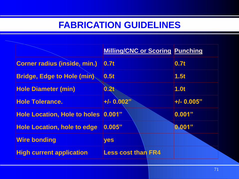
FABRICATION GUIDELINES
Milling/CNC or Scoring Punching
Corner radius (inside, min.) 0.7t 0.7t
Bridge, Edge to Hole (min) 0.5t 1.5t
Hole Diameter (min) 0.2t 1.0t
Hole Tolerance. +/- 0.002” +/- 0.005”
Hole Location, Hole to holes 0.001” 0.001”
Hole Location, hole to edge 0.005” 0.001”
Wire bonding yes
High current application Less cost than FR4
71

Specify Materials in Metal core; Comapny
name and part #.
Thickness of dielectric .
Tg or Td
Metal Core
Insulation resistance & Thermal conductivity
values.
Fabrication Check List
72

Footprints OR Data sheets
Net List
Material specifications
Construction Details
Layout Guideline
Mechanical Details
Other specific requirements
Fabrication Check List
73

CONCLUSION
Reduces Hot Spot
PCB acts as a Heat Sink
Reduces Thermal Stress on Components
Operates Cooler
SS or DS with SMT NO need to change the Design
74

Acknowledgements
Thanks to following contributors:
Laird Technology
Stabcor Inc. for their Stabcor laminates
75

Thank You
Presented By:
Pratish Patel
Electronic Interconnect
www.eiconnect.com
76