Advanced Techniques for PCIe 3.0 Receiver Testing · PDF filePCIe 2.x compliant channels shall...
47
Copyright © 2011, PCI-SIG, All Rights Reserved 1 Advanced Techniques for PCIe 3.0 Receiver Testing Michael Fleischer-Reumann BERTs Portfolio Planner Agilent Technologies
Transcript of Advanced Techniques for PCIe 3.0 Receiver Testing · PDF filePCIe 2.x compliant channels shall...

Copyright © 2011, PCI-SIG, All Rights Reserved 1
Advanced Techniques for PCIe 3.0 Receiver Testing
Michael Fleischer-Reumann
BERTs Portfolio Planner
Agilent Technologies

PCI-SIG Developers Conference Copyright © 2011, PCI-SIG, All Rights Reserved 2
Disclaimer Presentation Disclaimer: All opinions, judgments, recommendations, etc. that are presented herein are the opinions of the presenter of the material and do not necessarily reflect the opinions of the PCI-SIG®.

PCI-SIG Developers Conference
From PCIe 2.x to PCIe 3.0
Test Set-up and Calibration Methodology according to Base Specification
Practical set-up
Step-by-step Calibration Procedure
Summary
Q&A
Agenda
Copyright © 2011, PCI-SIG, All Rights Reserved 3

PCI-SIG Developers Conference
Effective data rate shall be doubled
Existing infrastructure of PCs and servers shall be reusable; in PCIe terminology this means:
PCIe 2.x compliant channels shall also be compliant with PCIe 3.0
Transmitting data at higher rate over the same channels means more loss causing closed eyes at the end of channel / receiver (RX) input
Method needs to be found opening the signal eye in order to
asses channel compliance
achieve functionality
Circuits and methods compensating channel loss have to be implemented in active components, Transmitter (TX) and Receiver (RX)
enhancing TX de-emphasis range and adding pre-shoot not sufficient
extensive RX equalization is necessary to achieve functionality
open source simulation tool (seasim) provides turnkey capability for channel assessment, where the user provides the channel characteristics at the receiver‟s die pad as step responses, and the tool calculates a statistical eye showing pass/fail.
From PCIe 2.x to PCIe 3.0 - Goals and Consequences
Go a l s
Consequences
Copyright © 2011, PCI-SIG, All Rights Reserved 4
PCI-SIG Developers Conference
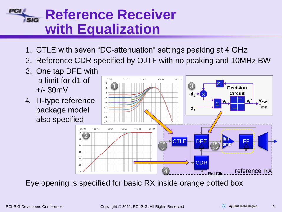
1. CTLE with seven “DC-attenuation“ settings peaking at 4 GHz
2. Reference CDR specified by OJTF with no peaking and 10MHz BW
3. One tap DFE with
a limit for d1 of
+/- 30mV
4. P-type reference
package model
also specified
Eye opening is specified for basic RX inside orange dotted box
reference RX
FF lim
amp
CDR
CTLE DFE TP
6
TP
2-P
Ref Clk
-16
-14
-12
-10
-8
-6
-4
-2
0
1E+07 1E+08 1E+09 1E+10 1E+11
-60
-50
-40
-30
-20
-10
0
1E+04 1E+05 1E+06 1E+07 1E+08 1E+09
x
Z-1
-d1
xk
yk yk*
S
Decision
Circuit
VEYE,
TEYE
2
1 3
4
Reference Receiver with Equalization
Copyright © 2011, PCI-SIG, All Rights Reserved 5

PCI-SIG Developers Conference
From PCIe 2.x to PCIe 3.0
Test Set-up and Calibration Methodology according to Base Specification
Practical set-up
Step-by-step Calibration Procedure
Summary
Q&A
Agenda
Copyright © 2011, PCI-SIG, All Rights Reserved 6

PCI-SIG Developers Conference
RX Test for PCIe 3.0 Generic Test Set-up
8 Gb/s
Pattern
Generator
BERT
RX-test itself is identical to that at lower data rates such as PCIe 2.x:
RX input is stimulated from a BERT PG with a “stressed eye“ signal containing well defined impairments
RX-output is looped back through the device‟s TX such that the RX‟s “correct” detection can be observed with a Bit Error Ratio Tester (BERT)
Construction / calibration of RX stress test signal is completely different utilizing methods and tools originally created for channel compliance verification
ASIC RX
DUT
TX
Ref
Clk
back to
BERT ED
Inte
rnal
Lo
op
bac
k
8 Gb/s
Error
Detector
Custom Test Board
Page 7 Copyright © 2011, PCI-SIG, All Rights Reserved 7

PCI-SIG Developers Conference
TP
6
RX Test-set-up acc. to PCIe 3.0 Base Spec.
ASIC RX
DUT
TX
Ref
Clk
Inte
rnal
Lo
op
bac
k
Custom Test Board
8 Gb/s
Pattern
Generator
Sinusoidal
Signal
Sources
Co
mb
ine
r
TP
1
The test generator shall be capable of generating the required Sinusoidal and Random Jitter (SJ and RJ)
It is complemented with signal sources for the simultaneous generation of Common- and Differential Mode Sinusoidal Interference (CM- and DM-SI) modeling the “noise” of the real application
They are superimposed to the test pattern through a passive combiner; output at TP1
Is TP6 suited for the calibration of the stressed eye RX-test signal?
Copyright © 2011, PCI-SIG, All Rights Reserved 8

PCI-SIG Developers Conference
Is TP6 suited for the calibration of the stressed eye RX-test signal? NO!
The PC board traces enabling connection of the DUT with test equipment (the so-called breakout channels) are not negligible in terms of signal degradation (DDJ) / (ISI)
Calibration must include the breakout channels
Connecting or probing for calibration of the stress signal directly at the ASIC pins / balls is not practical!
RX Test-set-up acc. to PCIe 3.0 Base Spec.
ASIC RX
DUT
TX
Ref
Clk
Custom Test Board
8 Gb/s
Pattern
Generator
Sinusoidal
Signal
Sources
Co
mb
ine
r
Breakout
Channel TP
6 TP
1
Copyright © 2011, PCI-SIG, All Rights Reserved 9

PCI-SIG Developers Conference
Structure of the test board with the so-called “Replica Channels” was defined
At the output of those there is the important test point TP2
TP2 is equivalent to the ASIC-input pins / balls as the replica channels duplicate the break-out channels
TP2 is the “closest point” to the RX inputs that can be measured of the RX test signals
RX Test-set-up acc. to PCIe 3.0 Base Spec.
ASIC RX
DUT
TX
Ref
Clk
Inte
rnal
Lo
op
back
Custom Test Board
8 Gb/s
Pattern
Generator
Sinusoidal
Signal
Sources
Co
mb
ine
r
TP
1
Breakout
Channel
Replica
Channel
TP
2
TP
5
TP
6
Copyright © 2011, PCI-SIG, All Rights Reserved 10
PCI-SIG Developers Conference
TP
2
Short Calibration Channel
Long Calibration Channel
TP
3
TP
4
8 Gb/s
Pattern
Generator
Sinusoidal
Signal
Sources
Co
mb
ine
r
TP
1
Breakout
Channel
ASIC RX
DUT
TX
Ref
Clk
Inte
rnal
Lo
op
back
TP
6
Custom Test Board
-25
-20
-15
-10
-5
0
1 1.5 2 2.5 3 3.5 4
Breakout Channel Only
Breakout + Short Calibration Channel
Breakout + Long Calibration Channel
Frequency / GHz
S21 /
dB
-20 ± 2dB
-12 ± 2dB
-2.5 ± 1dB -1.0 ± 1dB
-4.0 ± 1dB
-6.5 ± 1.5dB
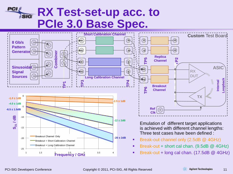
Emulation of different target applications is achieved with different channel lengths: Three test cases have been defined :
Break-out channel only (2.5dB @ 4GHz)
Break-out + short cal chan. (9.5dB @ 4GHz)
Break-out + long cal chan. (17.5dB @ 4GHz)
Replica
Channel
TP
5
RX Test-set-up acc. to PCIe 3.0 Base Spec.
Copyright © 2011, PCI-SIG, All Rights Reserved 11

PCI-SIG Developers Conference
RX Test Specifications for Stressed Jitter Eye
Symbol Parameter Limits at 8.0 GT/s Units Comments
VRX-LAUNCH-
8G
Generator
launch voltage
800 (nominal) mVPP Measured at TP1,
TRX-UI-8G Unit Interval 125.00 ps Nominal value is sufficient for Rx tolerancing.
Value does not account for SSC.
VRX-SV-8G Eye height at TP2P 25 (min)
35 (max)
mVPP At BER=10-12
TRX-SV-8G Eye width at TP2P 0.30 UI At BER=10-12
TRX-ST-SJ-8G Sinusoidal Jitter 0.1 – 1.0 UIPP Measured at TP1.
TRX-SV--RJ-8G Random Jitter 3.0 psRMS RJ spectrally flat before filtering. Measured at
TP1. Adjusted to set eye width
Copyright © 2011, PCI-SIG, All Rights Reserved 12

PCI-SIG Developers Conference
RX Test Specifications for Stressed Voltage Eye
Symbol Parameter Limits at 8.0 GT/s Units Comments
VRX-LAUNCH-8G Generator
launch voltage
800 mVPP Measured at TP1 Figure 4-65.
VRX-LAUNCH-8G may be adjusted if necessary to
yield the proper EH as long as the outside eye
voltage at TP2 does not exceed 1300 mVPP.
TRX-UI-8G Unit Interval 125.00 ps Nominal value is sufficient for Rx tolerancing. Value
does not account for SSC.
VRX-SV-8G Eye height at TP2P 25 (-20 dB channel)
50 (-12 dB channel)
200 (-3 dB channel)
mVPP Eye height @ BER=10-12
TRX-SV-8G Eye width at TP2P 0.3 to 0.35 UI Eye width at BER=10-12.
VRX-SV-DIFF-8G Differential mode
interference
14 or greater mVPP Adjusted to set EH. Frequency = 2.10 GHz..
VRX-SV-CM-8G Rx AC Common mode
voltage at 120MHz at TP2P
150 (EH < 100 mVPP)
250 (EH ≥ 100 mVPP)
mVPP Defined for a single tone at 120 MHz.
TRX-SV-SJ-8G Sinusoidal Jitter at 100
MHz
0.1 UIPP Fixed at 100 MHz.
TRX-SV--RJ-8G Random Jitter 2.0 psRMS Rj spectrally flat before filtering.
Copyright © 2011, PCI-SIG, All Rights Reserved 13

PCI-SIG Developers Conference
Calibration Method of Stressed Eye for RX Test
Replica
Channel TP
2
TP
5
TP2-P Add Behavioral
RX Package,
Equalizer and CDR
Custom Test Board Short Calibration Channel
Long Calibration Channel
TP
3
TP
4
8 Gb/s
Pattern
Generator
Sinusoidal
Signal
Sources
Co
mb
ine
r
TP
1
When using long calibration channel signal eye at TP2 is completely closed
Specifying stressed eye or jitter components at TP2 is therefore impractical
Specification of minimal tolerable eye opening refers to input of “basic receiver” inside the ASIC behind the reference RX‟s equalization (CTLE and DFE) and “jitter-filtering” with OJTF of RX-CDR (post processed signal of TP2 resulting in the signal at virtual test point TP2-P)
Calibration by measurement only is not possible
Combination of signal measurements and SW-simulation is required
Copyright © 2011, PCI-SIG, All Rights Reserved 14
PCI-SIG Developers Conference
Calibration Method of Stressed Eye for RX Test
Replica
Channel TP
2
TP
5
TP2-P Add Behavioral
RX Package,
Equalizer and CDR
Custom Test Board Short Calibration Channel
Long Calibration Channel
TP
3
TP
4
8 Gb/s
Pattern
Generator
Sinusoidal
Signal
Sources
Co
mb
ine
r
TP
1
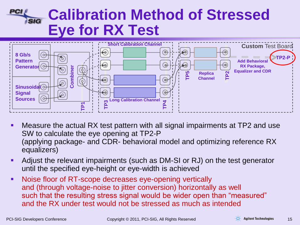
Measure the actual RX test pattern with all signal impairments at TP2 and use SW to calculate the eye opening at TP2-P (applying package- and CDR- behavioral model and optimizing reference RX equalizers)
Adjust the relevant impairments (such as DM-SI or RJ) on the test generator until the specified eye-height or eye-width is achieved
Noise floor of RT-scope decreases eye-opening vertically and (through voltage-noise to jitter conversion) horizontally as well such that the resulting stress signal would be wider open than “measured” and the RX under test would not be stressed as much as intended
Copyright © 2011, PCI-SIG, All Rights Reserved 15

PCI-SIG Developers Conference
Screenshots of test pattern with impairments turned on
Same scope setting 200mV/div
Pattern paused “visualizing“ DM-SI of 14mVpp at 2.1GHz
Reading of approx. 50mVpp !
Copyright © 2011, PCI-SIG, All Rights Reserved 16
Compliance pattern (800mV,pp) superimposed with DM-SI of 14mVpp at 2.1GHz
Scope setting 200mV/div (diff.) and a noise floor of approx. 4.7mVrms (diff.)
Accurate measurement of the stress signal at TP2 is impractical and error prone

PCI-SIG Developers Conference
Calibration Method of Stressed Eye for RX Test
TP
2
TP
5
TP2-P Add Behavioral
RX Package,
Equalizer and CDR
Custom Test Board Short Calibration Channel
Long Calibration Channel
TP
3
TP
4
8 Gb/s
Pattern
Generator
Sinusoidal
Signal
Sources
Co
mb
ine
r
TP
1
Divide the calibration of the RX stress signal into three separate steps:
1. Characterize the test set-up at TP2 using a test signal (clock/256), which allows averaging for noise reduction of RT-scope, resulting in a measured “step-response”
2. Use this step response as input for the statistical simulation SW that is also used for channel compliance verification and that calculates the eye opening for the final stress test signal (PRBS23) at a probability level of 10-12 after optimizing all equalizers and simulating impairments, iteratively finding the necessary amount of DM-SI or RJ that yields the specified eye-height (EH) or eye-width (EW)
3. Calibrate those impairments, which require calibration, one at a time, at the best suited test-point with the best suited test signal
Perform RX test with modified compliance pattern and all impairments turned on
Copyright © 2011, PCI-SIG, All Rights Reserved 17

PCI-SIG Developers Conference
Calibration of Stressed Eye for RX Test Flow chart w/ Statistical Eye Analysis Simulator (seasim)
Legend
HW
user or
auto-
mation
SW
seasim
RT-Oscilloscope
measures signal
at TP2 using
averaging
create step
response and
calculate IL of
test set-up adapt
amount of
DM-SI or RJ
EW and
EH ok?
simulate PRBS23 plus
default impairments
RJ, PJ, DM-SI and apply
CDR behavioral model
start
calibrate generator for
simulated values measuring
RJ, SJ at TP1 and
CM-SI and DM-SI at TP2 and
extrapolate the latter to TP2P
set up test generator :
• modified compliance
pattern
• impairments according to
- base specification
- results of seasim
simulation
yes
end of calibration
Run RX test
test generator
stimulates Clk/256
(128x”1”, 128x”0”)
into test set-up
calculate eye-opening
using statistical
simulator
apply behavioral package model
to step response and
import result into “seasim”
IL
within
range? yes no
if IL is
outside the
specified
range change
de-emphasis
up to +/- 2dB
or adapt set-
up and/or
cal. channels
optimize CTLE
and DFE for
max EW & EH
no verify test set-up
simulate stressed eye
calibrate impairments
and set up PG
Copyright © 2011, PCI-SIG, All Rights Reserved 18

PCI-SIG Developers Conference
Agenda
From PCIe 2.x to PCIe 3.0
Test Set-up and Calibration Methodology according to Base Specification
Practical set-up
Step-by-step Calibration Procedure
Summary
Q&A
Page 19 Copyright © 2011, PCI-SIG, All Rights Reserved 19

PCI-SIG Developers Conference
Two different RX Test Set-Ups (1 of 2) Stressed Jitter Eye
RJ-
source
SJ
source
8 Gb/s pattern
generator
w/ de-emphasis
Stressed jitter eye is testing RX for minimum horizontal eye opening (for long calibration channel plus break-out channel only)
Horizontal eye closure adjusted varying RJ
SJ varied according to specified curve
This set up is straight forward and can be realized with suitable BERTs
0
0.2
0.4
0.6
0.8
1
1.2
1.E+04 1.E+05 1.E+06 1.E+07 1.E+08
Breakout
channel
Cal.
channel
TP4 TP5 TP6 TP1
-20 dB IL at 4GHz
RX
DUT
SJ frequency/Hz
SJ
Am
pli
tud
e /
UI
Copyright © 2011, PCI-SIG, All Rights Reserved 20

PCI-SIG Developers Conference
Breakout
channel
Cal.
channel
TP4 TP5 TP6 TP1
-20 dB, -12dB, -2.5dB IL at 4GHz
RX
DUT
Two different RX Test Set-Ups (2 of 2) Stressed Voltage Eye
DM-SI RJ-
source
SJ
source
8 Gb/s pattern
generator
w/ de-emphasis
CM-SI
Combiner
Stressed voltage eye is testing RX for minimum vertical eye opening
(three possible combinations of calibration- plus break-out- channels)
Vertical eye closure is adjusted varying DM-SI
This test requires at least two additional voltage sources plus the
non-trivial combiner circuit
Copyright © 2011, PCI-SIG, All Rights Reserved 21

PCI-SIG Developers Conference
Realization for Voltage Interference Sources and Combiner
Combiner
Breakout
channel
Same electrical length and attenuation for both paths: otherwise CM DM
6dB 120MHz
CM-SI-source
6dB
6dB
2.1GHz
DM-SI-source
RJ-
source
SJ
source
8 Gb/s pattern
generator
w/ de-emphasis
Cal.
channel
TP4 TP5 TP6 TP1
-20 dB, -12dB, -2.5dB IL at 4GHz
RX
DUT
The most obvious realization for the CM-SI path
DM-SI path not shown for simplification
Copyright © 2011, PCI-SIG, All Rights Reserved 22

PCI-SIG Developers Conference
Transformation of CM- to DM-SI due to skew between “P” and “N”
VDM (t) = VCM,amp x {sin[wCMt] – sin[wCM(t - tskew])]}
sin(x) - sin(y) = 2 x cos((x+y)/2) x sin((x-y)/2)
VDM (t) = 2 x VCM,amp x cos(wCM(t - tskew/2)) x sin (wCMtskew/2)
VDM,amp = 2 x VCM,amp x sin (p x fCM x tskew)
0.00
2.00
4.00
6.00
8.00
10.00
12.00
14.00
16.00
0 10 20 30 40 50 60 70 80
VDM/mV
tskew/ps
Transformation of CM-SI into DM-SI
150
250
VCM/mV
In addition to DM-SI resulting
from skew between the two
sinewaves there is also DM-SI
resulting from different amplitudes
of the two sinewaves, which is
directly proportional to amplitude
and attenuation differences
Copyright © 2011, PCI-SIG, All Rights Reserved 23

PCI-SIG Developers Conference
Combiner
Breakout
channel
Same electrical length and attenuation for both paths: otherwise CM => DM
Desired signal path: CM-SI is split-up 50:50 into both P and N data paths with a total attenuation of 12dB as desired
6dB 120MHz
CM-SI-source
6dB
6dB
2.1GHz
DM-SI-source
RJ-
source
SJ
source
8 Gb/s pattern
generator
w/ de-emphasis
Cal.
channel
TP4 TP5 TP6 TP1
-20 dB, -12dB, -2.5dB IL at 4GHz
RX
DUT
Realization for Voltage Interference Sources and Combiner
The most obvious realization for the CM-SI path
DM-SI path not shown for simplification
Copyright © 2011, PCI-SIG, All Rights Reserved 24

PCI-SIG Developers Conference
Combiner
Breakout
channel
Same electrical length and attenuation for both paths: otherwise CM => DM
Desired signal path: CM-SI is split-up 50:50 into both P and N data paths with a total attenuation of 12dB as desired
Undesired signal path: P-data signal is coupled into N-data signal path (and vice versa) with an attenuation of 12dB relative to the data signal generating undesired broadband (DC-coupled) crosstalk
6dB 120MHz
CM-SI-source
6dB
6dB
2.1GHz
DM-SI-source
RJ-
source
SJ
source
8 Gb/s pattern
generator
w/ de-emphasis
Cal.
channel
TP4 TP5 TP6 TP1
-20 dB, -12dB, -2.5dB IL at 4GHz
RX
DUT
The most obvious realization for the CM-SI path
DM-SI path not shown for simplification
Realization for Voltage Interference Sources and Combiner
Copyright © 2011, PCI-SIG, All Rights Reserved 25

PCI-SIG Developers Conference
Combiner
Breakout
channel
Realization for Voltage Interference Sources and Combiner
Test set-up can be realized utilizing
BERT with internal jitter generation
Differential signal generator for DM-SI (or single ended source w/ balun)
Two separate sources for CM-SI generation avoiding crosstalk and allowing individual delay and amplitude adjust
External “plumbing“ for signal addition
6dB
6dB
6dB
6dB
2.1GHz
DM-SI-source
RJ-
source
SJ
source
8 Gb/s pattern
generator
w/ de-emphasis
Cal.
channel
TP4 TP5 TP6 TP1
-20 dB, -12dB, -2.5dB IL at 4GHz
RX
DUT
120MHz
CM-SI-source
120MHz
CM-SI-source
Final realization
Copyright © 2011, PCI-SIG, All Rights Reserved 26
PCI-SIG Developers Conference
Agenda
From PCIe 2.x to PCIe 3.0
Test Set-up and Calibration Methodology according to Base Specification
Practical set-up
Step-by-step Calibration Procedure
Summary
Q&A
Copyright © 2011, PCI-SIG, All Rights Reserved 27

PCI-SIG Developers Conference
PCIe3 Calibration
Channels
N4915A-014
xdB
xdB Breakout
channel
Cal.
channel
TP4 TP5 TP2 TP1
-20 dB, -12dB, -2.5dB IL at 4GHz
N4916B
CM
- +
2.1
GH
z D
M-S
I
Connect RT-Scope instead of DUT-RX
Generate clk/256 *)
Check IL for compliance with base spec.
If necessary, adjust de-emphasis (and amplitude) up to 2dB and re-check IL
*) BERT: DM-SI set to 0mV (don„t disable!) Function Generator either set amplitude to 0V or set into gating mode with threshold such that output is held constant (if amplitude cannot be set to 0V; disabling would disconnect 50 Ohm termination!)
N4903B
12
0M
Hz C
M-S
I
Calibration of Stressed Eye
81150A
Copyright © 2011, PCI-SIG, All Rights Reserved 28

PCI-SIG Developers Conference
. . .
Copyright © 2011, PCI-SIG, All Rights Reserved 29
Interpretation of Calibration Channel Specification

PCI-SIG Developers Conference
Long Cal. Channel with 0dB and -1.5dB De-emphasis
step response dv/dt =
impulse response
FFT = Insertion loss
1.Check IL of test
set-up:
differentiating
step response
and doing FFT of
the resulting
impulse response
2.Measured IL too
large (~21.5dB)!
3.Correct with
appropriate de-
emphasis of -
1.5dB of post
cursor
and adjust
amplitude for
same end value
of step response
4. Insertion loss of
adjusted set-up ~
20.0dB Copyright © 2011, PCI-SIG, All Rights Reserved 30
de-emphasis = -1.5dB
de-emphasis = 0 dB

PCI-SIG Developers Conference
Apply the
reference
package model
(IL @ 4GHz ~
3.2dB)
and import
waveform in
appropriate form
into seasim!
Long Cal. Channel + Ref. Package
Copyright © 2011, PCI-SIG, All Rights Reserved 31
with ref. package

PCI-SIG Developers Conference
Construction and Calibration of stress signal
Disconnect all signals from scope input (terminate with 50 Ohms)
1. Measure* scope intrinsic noise Vn,intrinsic
Turn on all sources, set generator to “pause“-pattern / set amp=0V (“disable“ outputs)
2. Measure* Noise Voltage Vn,system and determine noise of generators as Vn,gen = sqrt (Vn,intrinsic
2 - Vn,system
2)
* always apply ref. package model
Copyright © 2011, PCI-SIG, All Rights Reserved 32

PCI-SIG Developers Conference
Differential Noise Voltage
Scope Noise Vn,intrinsic = 640 µVrms
System Noise = Vn = 754 µVrms
Vn,gen = sqrt (Vn,intrinsic2
- Vn,system2) = 399 µVrms
Copyright © 2011, PCI-SIG, All Rights Reserved 33

PCI-SIG Developers Conference
Seasim Parameters
Copyright © 2011, PCI-SIG, All Rights Reserved 34
RJ
SJ
DM-SI
Vn,gen

PCI-SIG Developers Conference
Seasim calibration for stressed voltage test, long cal channel
starting value for DM-SI = 14mV
resulting in ~27mV of eye height (EH)
“SW-adjusted“ value for DM-SI = 16mV
resulting in ~25mV of EH w/ (0.3UI<EW<0.35UI)
Copyright © 2011, PCI-SIG, All Rights Reserved 35
PCI-SIG Developers Conference
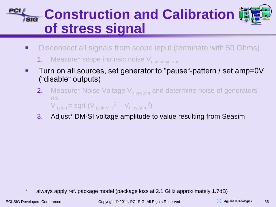
Construction and Calibration of stress signal
Disconnect all signals from scope input (terminate with 50 Ohms)
1. Measure* scope intrinsic noise Vn,intrinsic,rms
Turn on all sources, set generator to “pause“-pattern / set amp=0V (“disable“ outputs)
2. Measure* Noise Voltage Vn,system and determine noise of generators as Vn,gen = sqrt (Vn,intrinsic
2 - Vn,system2)
3. Adjust* DM-SI voltage amplitude to value resulting from Seasim
* always apply ref. package model (package loss at 2.1 GHz approximately 1.7dB)
Copyright © 2011, PCI-SIG, All Rights Reserved 36

PCI-SIG Developers Conference
Calibration of 2.1G DM-SI
16.188 mV
16.093 mV
15. 143mV
17.058 mV
Copyright © 2011, PCI-SIG, All Rights Reserved 37
As Vn,gen (noise
from generator)
is taken care of
by vn_lfrn in
seasim,
averaging can be
used for
calibration of
DM-SI

PCI-SIG Developers Conference
Construction and Calibration of stress signal
Disconnect all signals from scope input (terminate with 50 Ohms)
1. Measure* scope intrinsic noise Vn,intrinsic,rms
Turn on all sources, set generator to “pause“-pattern / set amp=0V (“disable“ outputs)
2. Measure Noise Voltage Vn,system and determine noise of generators as Vn,gen = sqrt (Vn,intrinsic
2 - Vn,system2)
3. Adjust DM-SI voltage amplitude to value resulting from Seasim applying ref. package model (package loss at 2.1 GHz approximately 1.7dB)
4. Adjust CM-SI amplitude to specified value (150 or 250mV) (also applying ref package model) adjust delay (and amplitudes) of CM-SI generator for minimum residual differential amplitude
* always apply ref. package model
Copyright © 2011, PCI-SIG, All Rights Reserved 38

PCI-SIG Developers Conference
CM-SI calibration of residual DM
CM-SI, 120MHz 150mV
remaining DM –“noise“
Copyright © 2011, PCI-SIG, All Rights Reserved 39

PCI-SIG Developers Conference
Construction and Calibration of stress signal
Disconnect all signals from scope input (terminate with 50 Ohms)
1. Measure* scope intrinsic noise Vn,intrinsic,rms
Turn on all sources, set generator to “pause“-pattern / set amp=0V (“disable“ outputs)
2. Measure* Noise Voltage Vn,system and determine noise of generators as Vn,gen = sqrt (Vn,intrinsic
2- Vn,system2)
3. Adjust* DM-SI voltage amplitude to value resulting from Seasim applying ref. package model (package loss at 2.1 GHz approximately 1.7dB)
4. Adjust* CM-SI amplitude to specified value (150 or 250mV) (also applying ref package model) adjust delay (and amplitudes) of CM-SI generator for minimum residual differential amplitude
Set generator to clock/2 pattern
5. Turn on RJ and SJ each at a time and sequentially adjust* them to specified values measuring either at TP1 or TP2
* always apply ref. package model
Copyright © 2011, PCI-SIG, All Rights Reserved 40

PCI-SIG Developers Conference
Calibration of RJ
Copyright © 2011, PCI-SIG, All Rights Reserved 41

PCI-SIG Developers Conference
Calibration of RJ and SJ
Copyright © 2011, PCI-SIG, All Rights Reserved 42

PCI-SIG Developers Conference
Calibration accomplished - ready to perform the RX test
Disconnect cables fromTP5 (input replica channel) and connect to TP6 (input breakout channel)
Set DUT-RX into loopback
Turn on all impairments as calibrated and make BERT-PG generate the test pattern (modified compliance pattern)
Verify number of errors for sufficient time period such that BER<10-12 w/ 95% of CL e.g.: 0 errors in 6¼ minutes 1 error in 10¼ minutes 2 errors in ...
Copyright © 2011, PCI-SIG, All Rights Reserved 43

PCI-SIG Developers Conference
Agenda
From PCIe 2.x to PCIe 3.0
Test Set-up and Calibration Methodology according to Base Specification
Practical set-up
Step-by-step Calibration Procedure
Summary
Q&A

PCI-SIG Developers Conference
Summary
PCIe 3.0 Phy Layer system design with its 8GT/s was relatively demanding, its realization in a computer system is not trivial
Interoperability depends on proper RX functionality and can only be guaranteed by thorough RX testing
Test set-up must be designed with great care
Calibration of stress test signal requires deep insight into base specification and measurement techniques
Performing “step-by-step calibration“ manually is cumbersome and error prone – automation desirable
Copyright © 2011, PCI-SIG, All Rights Reserved 45

PCI-SIG Developers Conference
Agenda
From PCIe 2.x to PCIe 3.0
Test Set-up and Calibration Methodology according to Base Specification
Practical set-up
Step-by-step Calibration Procedure
Summary
Q&A
Copyright © 2011, PCI-SIG, All Rights Reserved 46

PCI-SIG Developers Conference Copyright © 2011, PCI-SIG, All Rights Reserved 47
Thank you for attending the PCI-SIG Developers Conference 2011.
For more information please go to www.pcisig.com