
Advanced Space Communications I Architecture Study · PDF fileAdvanced Space Communications...
190
I i I I I Advanced Space Communications Architecture Study I ! Volume 2 - Technical Report i i ! I NASA CR 179592 IJI _. --L 4 N N'/ I¥1i:11t;il I_OI i I I I I Prepared for National Aeronautics and Space Administration Lewis Research Center Cleveland, OH 44135 I I Prepared by TRW Eiectromc Systems Group One Space Park Redondo Beach, CA Y0278 I https://ntrs.nasa.gov/search.jsp?R=19870009262 2018-04-25T23:13:37+00:00Z
Transcript of Advanced Space Communications I Architecture Study · PDF fileAdvanced Space Communications...

I
iI
I
I
Advanced Space CommunicationsArchitecture Study
I
!Volume 2 - Technical Report
i
i
!
I
NASA CR 179592
IJI _. --L 4 N N'/
I¥1i:11t;il I_OI
i
I
I
I
I
Prepared forNational Aeronautics and Space AdministrationLewis Research CenterCleveland, OH 44135
I
IPrepared by
TRW Eiectromc Systems GroupOne Space ParkRedondo Beach, CA Y0278
I
https://ntrs.nasa.gov/search.jsp?R=19870009262 2018-04-25T23:13:37+00:00Z

I
II
II
II
!I
II
II
II
II
Advanced Space CommunicationsArchitecture Study
Volume 2 - Technical Report
NASA CR 179592
March 1987
PreparedforNational Aeronautics and SpaceAdministrationLewis ResearchCenterCleveland,OH44135
Prepared byTRW Electronic Systems GroupOne Space ParkRedondo Beach, CA 90278

I
II
II
I
II
II
Advanced Space CommunicationsArchitecture Study
Volume 2- Technical Report
NASA CR 179592
March 1987
Prepared by Prepared for
| TRW Electronic Systems Group NASA Lewis Research CenterOne Space Park 21000 BrookparkRoad
| RedondoBeach, CA 90278 Cleveland,OH 44135
!Approved:
!
' _Y-_ c-__,_'__,__- -M.G. Davis, Jr.
I Principal Investigator Manager, Electronic Development Operation
II

I
I
I
I
I
I
I
I
I
I
I
I
I
I
I
I
I
I
I
.
2.
3.
4.
5.
6.
7.
8.
TABLE OF CONTENTS
Introduction
System Description and Analysis
2.1 System Concept
2.2 Link Design
2.3 SatelliteReceive Antenna
2.4 Bulk Demodulators
2.5 SatelliteTransmit Antenna
2.6 Baseband Multiplexer
Satellite Receive Antenna Design3. I MBA with Multiple Reflectors
3.2 MBA with MultipleLenses
Satellite Transmit Antenna Design
4.1 Phased-Array-Fed Reflector Antenna
4.2 Active-Aperture Phased Array
4.3 MBA with Beam Switching Matrix
4.4 Comparison of Antenna Configurations
Bulk Demodulator Technology5.1 SAW Demodulators
5.2 FFT Demodulators
5.3 Conclusions
Baseband Multiplexer Technology
6.I High-Speed SerialTime-Domain Multiplexers
6.2 Frequency-Domain Multiplexers
6.3 Memory-Based Multiplexers
Transmitter and Receiver Technology
Satellite Weight and Cost
8.1 Payload Weight
8.2 SatelliteWeight
8.3 SatelliteCost
Page i
pa_a_
1-1
2-1
2-1
2-4
2-9
2-12
2-17
2-26
3-I
3-3
3-8
4-I
4-I
4-14
4-25
4-32
5-I
5-2
5-12
5-22
6-I
6-3
6-6
6-11
7-I
8-I
8-I
8-14
8-19
,
10.
11.
TABLE OF CONTENT5 - continued
User Terminal Design and Cost
9.I Terminal Description
9.2 Key Design Issues
9.3 Terminal Cost
5ubscriber Charge
Conclusions
Page ii
9-I
9-2
9-8
9-II
10-I
11-I
I
I
I
I
I
I
I
I
I
I
I
I
I
I
i
I
I
I
I

II
I
II
II
I
III
I
II
II
III
6-I
8-I
8-2
8-3
8-4
8-5
8-6
8-7-
8-8
8-9
8-10
8-11
9-I
9-2
9-3
10-I
10-2
10-3
10-4
10-5
LIST OF TABLES
Uplink Power Budget (29.5GHz)
Downlink Power Budget (19.7GHz)
EIRP for Array-Fed Dual Reflector Antenna
EIRP for Active-Aperture Phased Array
Typical MultiplexerRequirements
Payload Weight and Power Summary
ReceiverlDemultiplexer Weight and Power Estimate
Modulator Weight and Power Estimate
Array-Fed Dual Reflector Antenna Weight and PowerEstimate
Satellite Power Requirements
Satellite Weight vs. Eclipse Capability
Satellite Weight Budget
Thermal Control Subsystem Weight
Satellite Cost Summary
Payload Cost Summary
Spacecraft Bus Cost 5ummary
LNA Implementation Tradeoff
Unit Cost Estimates
User Terminal Cost Estimate
Traffic and User-Terminal Profiles
Assumptions for Service Charge Calculation
Program Expenditure Profilefor Minimum Number of
Terminals
Required Revenue ($000 per Channel-Year)
Subscriber Service Charge (¢ per Channel-Minute)
Page iii
4-11
4-18
6-2
8-3
8-6
8-12
8-13
8-15
8-16
8-17
8-18
8-20
8-22
8-23
9-9
9-12
9-13
10-2
I0-6
10-9
10-14
10-15

LIST OFFIGURES
I-I Satellite Links
2-I2-22-32-4
2-5
2-6
2-7
2-8
2-9
2-10
3-I
3-2
3-3
4-I
4-2
4-3
4-4
4-5
4-6
4-7
4-8
5-I
5-2
5-3
5-4
5-5
5-6
5-7
5-8
5-9
i-3
SatellitePayload FunctionalBlock Diagram 2-3
UplinkBeam Pattern 2- I I
SingleFFT-Bulk-Demodulator Power Requirements 2-14
Bulk Demodulator Power Requirements for Composite 2-16
IO00-MHz Bandwidth
Phased-Array-Fed Gregorian Reflector Antenna 2-19
RF Power Requirements forMagnification Factor of 2 2-2i
RF Power Requirements for Magnification Factor of 3 2-22
Main Reflector Diameter for Array-Fed Dual Reflector 2-23Antenna
Two-Antenna Transmit Configuration 2-24
Onboard Data Storage Versus Downlink-Beam Switch Time 2-28
Uplink Beam Pattern
Offset-Fed Reflector Antenna Geometry
Multiple-Lens Antenna Geometry
Array-Fed Dual Reflector Antenna System
Phased Array Transmit Modules
Radiating Horn Edge-of-Coverage Gain
Hexagonal Array EIRP
Linear Array Equivalents to Hexagonal Array
MBA with Beam Switching Matrix
Triangular Beam Pattern
Beam Interlacing with Four-Aperture Antenna System
SAW Demodulator
Compressive Receiver Block Diagram
Reflexive Array Compressor (RAC) Operation
High Degree of Correlation Between Model and Hardware
Recursive FFT Using VHSIC I Chips
Pipelined FFT Block Diagram
Image Signals Due to Phase and Amplitude Mismatch
Effect of Amplitude and Phase Mismatch on Signal-to-
Image Ratio (SIR)
Presumming Calculations
Page iv
3-2
3-4
3-9
4-2
4-3
4-16
4-21
4-22
4-26
4-27
4-29
5-3
5-5
5-6
5-8
5-14
5-16
5-17
5-19
5-21
I
I
I
I
I
I
I
I
I
I
I
I
I
I
I
I
I
I
I

I
II
Ii
II
I
III
I
II
II
IIi
6-I
6-2
6-3
6-4
6-5
6-6
7-I
7-2
7-3
7-4
7-5
7-6
7-7
8-I
8-2
8-3
9-I
9-2
9-3
10-I
10-2
10-3
10-4
10-5
10-6
LIST OF FIGURES- continued
Bulk Demodulator and Buffer for Time-Domain Multiplexer 6-5
Time-Domain Multiplexer SerialInterconnection 6-7
Time-Domain Multiplexer ParallelInterconnection 6-8
Frequency-Domain Multiplexer 6-9
Address-Pointer Memory-Based Multiplexer 6-13
(Wire-OR Version)
Raster Output Memory-Based Multiplexer 6-15
Device Power Level Projections
Device Efficiency Projections
Solid-State Amplifier Design Example
Device Noise Figure Projections
Device Gain Projections
TRW HEMT Performance Projections
Low-Noise Amplifier Design Example
Satellite Payload Functional Block Diagram
Receiver/Demultiplexer Block Diagram
Modulator Block Diagram
User Terminal Block Diagram
User Terminal Configuration
IMPATT Amplifier Design
7-2
7-3
7-5
7-7
7-8
7-9
7-10
8-2
8-4
8-II
9-3
9-4
9-10
Page v
Satellite Development and Manufacturing Schedule 10-8
Program Expenditures for Minimum Number of Terminals 10- I 1
Program Expenditures for Twice Minimum Number of 1O- 12Terminals
Program Expenditures for Three Times Minimum Number ! 0-13of Terminals
Nondiscounted Cash-Flow Profile for Minimum Number of 10-18
Terminals
Discounted Cash-Flow Profile for Minimum Number of 10-19
Terminals

III
!l
II
I
lI
II
II
Ii
IIi
1. INTRODUCTION
Until recently, it was generally believed that trunking traffic would
domlnate polnt-to-polnt satelllte communlcatlons. Because of the rapid
progress In fiber optlcs communlcatlons, however, It Is now clear that
trunklng traffic wlll, for the most part, be carrled terrestrlally rather
than by satelllte. In the future, therefore, polnt-to-polnt satelllte
communlcatlons wlll be domlnated by thln-route appllcatlons Involving
flxed or moblle termlnals.
NASA's Advanced Communlcatlons Technology Satelllte (ACTS)
program was concelved durlng the perlod when trunklng trafflc was the
domlnant point-to-point satellite mode. Accordingly, ACTS is intended to
advance technology development In both trunklng systems and customer
premlse service (CPS). The latter servlce Is Intended to provide satellite
volce and/or data llnks dlrectly between end users, thereby obviating
constructlon of terrestrlal talls between earth station and end user. Wlth
the anticipated demlse of satelllte trunklng, the CPS aspect of ACTS is the
more relevant to future satelllte communlcatlons.
Thls reportpresents the resultsof a 12-month study to determine
satellite system architectures that are most suitable for CPS
communications. As with ACTS, the focus Is on 30120-GHz (Ka-band)
technology. However, the system architecturesexamined are equally
applicabletooperationat 14/II GHz (Ku-band).Because largenumbers of
Page I-I

users (i.e., 10,000 or more) are intended to be served, emphasis is placed
on system designs that permlt low user terminal costs.
The satellite links In the type of system under consideration are
shown In Figure 1-1. Complete "single-hop" lnterconnectivity, whlch ls
needed for voice communications, ls provided between any pair of system
users. To establish such a connection, a user requests elther a one-way
channel or a two-way circuit, as needed, from the master control station.
These requests are transmitted over an orderwire channel, typically
making use of a random access protocol. When the circuit is no longer
needed, It ls restored to the pool of clrcults available for reassignment.
Minimization of terminal costs generally Implies low values of peak
EIRP. It ls also Important to llmlt the terminal size, since real estate and
Installation costs might otherwise outweigh termlnai equipment costs.
The terminal antenna diameter ls llmlted to 1.2m in most of continental
United States (CONUS), although l.Sm antennas are permitted In
heavier-rainfall areas to malntain system availability. A
frequency-division multiple access (FDMA) upllnk signal format ls
selected because It permits narrow-bandwidth transmission, which tends
to mlnlmlze EIRPrequirements.
Single-hopinterconnectlvltyrequiresthat the satelliteact llkea
switchboard in the sky,wlth accessabllityto each individualterminal
transmission,The acceptedmeans ofprovidingthlsaccessablllty(andthe
^n,, ArnnIA,,,-,,l I_,, C_I ie tirn_,-rliui_inn multipleaccess (TFIHAI,,,,_,.,,,_,,,,y_,,yACT.,,,.,use of a .......................
transmissionformat.The use ofFDMA, on the otherhand,heretofore
Page I-2
I
I
I
I
I
I
I
I
I
I
I
II
I
I
I
I
II

I
I
! /
/
I
II
I
II
\\
\\
\\
I Page 1-3

would have required a separate satellitedemodulator for each terminal
transmission. However, the prospect now exists for the development of
"bulk" demodulators of sufficiently low power consumption to be
attractive for satellite use. A bulk demodulator a_cepts as input a
composite FDMA signal and provides a tlme-dlvision multiplexed (TDM)
pulse stream in which the demodulated bits of the various input carriers
are Interleaved.Thus, the demodulator output has a format similar to that
of the uplInktransmissions In a TDMA system. A single bulk demodulator
might simultaneously process 100 FDMA carriers, thereby providing a
100:1 reduction In the number of demodulators that would otherwise be
required.
In contrast to the upllnk,downllnk transmission Is accomplished by
means of a small number of wideband, TDM carriers. A baseband processor
buffers the relatlvely large number of demodulator outputs and
multiplexes them onto the downlIn.kcarriers.
The satellite transmit antenna is designed to have a relatively high
galn (l.e., small beamwldth), to mlnlmlze the transmlt power
requlrements. In addltlon, the small spot slze produced by the antenna
permits the Introductlon of frequency reuse, whlch expands the effectlve
system bandwidth. A separate antenna beam is generated for each
downlink carrier. Each beam is "hopped" among the downlink spots,
dwelling on each spot long enough to transmit a predetermined number of
bits from each 64-kbps upllnk carrier Intended for one of the termlnals
_A_,II.I_t_ t-k,_ ,,',._,._t- k,-,.._,.,l-..,,,,_,VV II.,11111 _,11_ _l, JIJ_, I,Jt,JUl II, J_l )/*,
Page I- 4
I
I
I
I
I
I
I
I
I
I
I
I
I
I
I
I
I
I
I

III
II
I
II
I
I
II
II
II
III
A complete system descriptionand a number of key system tradeoffs
are presentedInSection2. Detailsof thesatellitereceiveand transmit
antennadesignsare presentedir_Sections3 and 4,respectively.The bulk
demodulatortechnologyIsexamined InSection5, the baseband processor
technologyInSection6,and transmitter/recelvertechnologyat 30120 GHz
InSection7.
Sections 8 to II are concerned wlth the financial aspects of system
implementation and operation. The weight of each payload element,
together wlth a satelllte subsystem welght budget, Is presented In Section
8. Nonrecurrlng and recurring satelllte cost estlmates, derived from the
welght estlmates, are also provlded In Section 8. A user terminal design
and cost estlmate are glven In Section 9. Sectlon I0 derives the user
service charge needed to provlde a speclfled rate of return on Invested
capital, based on an assumed traffic profile. The study conclusions are
stated In Section I I.
Page I- 5

II
II
II
II
II
II
II
II
II
I
2. SYSTEH DESCRIPTION AND ANALYSIS
Because the ground segment is a major system cost driver, the first
step in defining a system concept is to select an appropriate set of user
terminal parameters. By means of the link equations, corresponding
satellite receive antenna gain and EIRP requirements are then obtained to
satisfy the system performance objectives. Subject to the derived
satellite requirements, a number of satellite subsystem trades are
performed to arrive at a complete system description.
2.1. System Concept
Each terminal is provided the capability to transmit a single
narrowband digital carrier. The minimum or standard data rate is taken as
64 kbps. The carriers transmitted by the various terminals are
distinguished by frequency and/or polarization. Thus, the uplink signal set
comprises a large number of FDMA carriers spread over the 500-MHz
Ka-band fixed-satellite allocation not shared with the fixed (terrestrial)
service. Since dual polarization is used, the equivalent composite
bandwidth is 1000 MHz.
With present-day digital voice representations, the 84-kbps terminal
transmission can support two voice channels. With the higher-speed
digital circuitry expected by the end of the decade, 18-kbps digital voice
should replace the current 32-kbps voice standard. Each terminal will
then be capable of transmitting four voice channels. Hore generally, a
terminal could support various combinations of voice and data totaling. 64
Page 2- I

kbps. The constituents of the 64-kbps transmission need not be directed
at the same terminal. With QPSK transmission employed on the uplink (see
Section 2.2), the in-phase and quadrature components are readily
separated in the satellite and retransmitted to different terminals.
A functional block diagram of the satellite payload is shown in Figure
2-I. The satellite receive antenna produces a number of fixed area beams
which provide complete CONUS coverage. The carriers received on a given
beam are divided into groups of standard size, each of which is input to a
bulk demodulator. The latter converts a set of FDMA signals, contiguous in
frequency, to a single TDM pulse stream in which pulses corresponding to
an individual input signal are interleaved with those of all other inputs.
The demodulator bandwidth is chosen narrow enough so that the traffic
handling capability of each beam can be matched to the traffic offered
through assignment of an appropriate number of demodulators. Allowing a
certain number of demodulators to be switchable between beams leads to
accommodation of an epr/or/unknown or time-varying traffic pattern.
The bulk demodulator outputs are fed to a baseband multiplexer which
buffers and sorts the data bits according to the downlink beam for which
they are intended. The number of downlink beams is considerably smaller
than the number of spots (as measured by the antenna beamwidth) needed
to cover CONUS. Each downlink beam is therefore programmed to scan over
a portion or all of CONUS in a repetitive pattern. The data bits assigned to
a beam for transmission during one complete scan are organized according
to the downlink spot for which they are intended. In this way, no spot is
Page 2-2
I
I
I
I
I
I
II
I
I
I
III
I
II
II

I
I ¥ ? _ f7I I, =_=X I[ =_=x I---L =_-"_J I =_=x i
41'OQ _ •!
, f II _ I=---o_=1 L_---o:_ ]I
| _
' ., ii| _ •
| _t_ 000
ft.
I
I .
I "'" )
I
IPage 2-3

visited more than once per scan by any of the beams.
As depicted in Figure 2-I, each downlink beam is formed by
power-dividing the corresponding carrier and feeding the resulting signals
to modules associated with the radiating elements. Each module consists
of an amplifier and a variable phase shifter. Each radiating element is
excited by the combined output of several modules, one for each downlink
beam. The set of radiating elements can either form a direct-radiating
array or be used as an array feed for a reflector type of antenna.
2.2. Link Design
The user terminals are equipped with 1.2m antennas. This size is
typical of very-small-aperture-terminal (VSAT) design. Each terminal
that transmits the standard 64-kbps carrier has a 2W transmitter. This
power levelisabout the maximum achievable at reasonable cost. Both the
terminal and the satellite are equipped with HEMT LNAs. The
corresponding receiver noise figures are projected to be 2.0 dB and 3.0 dB,
respectively.
Considerable uncertainty exists concerning the rain margin required
to achieve a specified link availability. The margins selected are intended
to correspond to an uplink or downlink availability of 0.995 in all but the
southeast portion of CONUS (Rain Zone E), as reported in Reference 2-I.
Accordingly, no end-to-end transmission path has an availability of less
than o.gg. In fact, most composite paths have considerably higher
availability. An antenna diameter of 1.8m is required to extend 0.995 link
availability to Rain Zone E.
Page 2-4
I
I
I
I
I
I
I
I
I
I
I
I
I
I
I
I
I
I
I

III
!I
II
I
iI
II
II
II
Iii
A higher link availability than 0.995 was not selected because of the
impact on the satellite design. Improving the link availability to 0.9975
(i.e., halving the link outage) requires uplink and downlink margins of about
15 dB and 6 dB, respectively, compared with 8 dB and 4 dB for a link
availability of 0.995.
To maximize system capacity, QPSK transmission is used on the
uplink. The data is differentially encoded to simplify the demodulation
process on the satellite. On the downlink, the choice of modulation is
dictated by the need to minimize the cost, and hence the complexity, of the
receive portion of the user terminals. To this end, differential data
encoding is essential. BPSK is selected in place of QPSK because of the
larger Eb/N o requirement associated with differential QPSK. The larger
carrier bandwidth associated with BPSK transmission necessitates a
degree of spatial frequency reuse, in addition to polarization diversity.
This requirement imposes an operational constraint on the downlink-beam
scanning patterns, if excessive interbeam interference is to be avoided.
To provide the requisite link quality, assumed to correspond to a BER
of 10-7, end-to-end error correction coding is employed. Use of
soft-decision decoding on the ground would be largely negated by the
demodulation process on the satellite. Therefore, hard-decision decoding
is used instead.
Because of the relatively small EIRP and G/T of a 1.2m terminal, it is
desirable to obtain as much coding gain as possible. On the other hand, a
lower code rate leads to a larger bandwidth per carrier and therefore
Page 2-5

smaller system capacity.
rate-3/4 coding.
These opposing factors lead to a choice of
Uplink and downlink power budgets are given in Tables 2-1 and 2-2.
Each link is nominally designed for a decoded BER of 10-7 (a fictitious
quantity in the case of the uplink). The end-to-end error rate of the
undecoded transmissions is twice that of either the uplink or the downlink
considered separately. Therefore, the BER of the decoded transmissions
will in fact be somewhat greater than 10 -7 .
The required values of Eb/N o in Tables 2-1 and 2-2 include an
implementation margin (i.e., departure from theoretical) of 3 dB. In
addition, the Eb/N o penalty due to differential data encoding is 2.3 dB on
the uplink (for QPSK) and 0.6 dB on the downlink (for BPSK).
The required uplink signal quality is achieved by proper design of the
satellite receive antenna, while the downlink signal quality depends on
proper selection of the satellite EIRP. Accordingly, the receive antenna
gain must be at least 33.3 dB throughout CONUS. For the selected downlink
data rate of 180 Mbps per beam, the satellite EIRP must be at least 63.1
dBW.
The choice of 180 Mbps for the downlink data rate is governed by the
desire to accommodate the downlink data on four carriers. As will be seen
in Section 4, this downlink data partitioning leads to use of two identical
Page 2-6
!
I
I
!
I
I
I
I
i
II
II
II
II
II

I
II!
II
II
I!
I
II
III
II
i
TABLE 2-I. UPLINK POWER BUDGET (29.5 GHz)
Transmitter power (2W), dBW
Line loss,dB
Antenna gain (1.2m),dB
Pointing loss,dB
EIRP, dBW
Path loss,dB
Atmospheric loss,dB
Rain loss (.995 except Zone E),dB
SIC antenna gain (edge of beam) plus linelosses,dB
Received carrierpower, dBW
System noise temperature, dB-K
Boltzmann's constant, dB (WIK-Hz)
No,dB (WIHz)
Bit rate (64 kbps),dB (sec-1)
EblN o,dB
Page 2-7
3.0
-1.0
49.2
-1.0
50.2
-213.7
-0.6
-8.0
33.3
- 138.8
27.6
-228.6
-201.0
48.I
14.1

TABLE 2-2. DOWNLINK POWER BUDGET (19.7 GHz)
EIRP, dBW
Path loss, dB
Atmospheric loss, dB
Rain loss, dB
E/S antenna gain, dB
Pointing loss, dB
Line loss, dB
Received carrier power, dBW
System noise temperature, dB-K
Boltzmann's constant, dB (W/K-Hz)
No, dB (W/Hz)
Bit rate ( 180 Mbps), dB (sec- 1)
Eb/N o, dB
Page 2-8
63.1
-210.2
-0.8
-4.0
45.8
-0.8
-10
- 107.9
-202.9
82.6
12.4
I
I
I
i
I!i
I
I!
!
I
I
I
I
I
I
I
I

I
II
!
II
iI
I!
!I
II
II
iI
I
transmit antennas, each radiating a pair of carriers on opposite
polarization. The downlink data rate is therefore one-fourth of the total
satellite throughput.
The satellite throughput is determined by uplink considerations. Each
uplink carrier supports a data rate of 64 kbps. With QPSK transmission
and rate-3/4 coding, the transmitted symbol rate is 42.67 ksps. For
purposes of bulk demodulation, the carrier separation must be twice the
transmitted symbol rate, or 85.33 kHz. The effective system bandwidth of
l O00 MHz accommodates 11,718 such carriers or, equivalently, a
composite data rate of 750 Mbps. Allowing 30 Mbps for system overhead
leaves 720 Mbps as the system throughput rate. The downlink data rate is
therefore !80 Mbps per beam.
Two 180-Mbps carriers are transmitted on each polarization. With
rate-3/4 coding and BPSK modulation, each carrier supports a
transmission rate of 240 Msps. With a bandwidth-to-symbol rate ratio of
(say) 1.5, each downlink carrier occupies 360 MHz. With a 500-MHz
allocation on each polarization, the two carriers clearly have overlapping
spectra. As observed earlier, this overlap places constraints on the
downlink-beam scanning patterns.
2.3. Satellite Receive Antenna
From Table 2-1, the satellite receive antenna must provide a
minimum gain over CONUS of 33.3 riB. This minimum gain determines the
required number of uplink beams. For a given angular coverage, the gain at
beam edge is maximized if it is chosen 4.3 dB less than the peak gain.
Page 2-9

Therefore, the peak gain must be 37.6 dB. This gain provides beam
coverage (i.e., 4.3-riB beamwidth) of 2.56 degrees. Approximately eight
such beams, forming the pattern shown in Figure 2-2, are needed for
CONUScoverage.
The portion of the frequency .allocation, and correspondingly the
number of bulk demodulators, assigned to each uplink beam is proportional
to the traffic offered by user terminals located within the beam coverage
area. The frequency band assigned to a given beam may be confined to a
single polarization or divided between the two polarizations. The first
alternative requires only a single port per feed horn (rather than a
separate port for each polarization) and leads to a simpler repeater
configuration. For this reason, it has been chosen for the baseline
satellite configuration.
It should be pointed out, however, that confining each beam to a
single polarization has the effect of dividing the total available bandwidth
of 1000 MHz into two distinct 500-MHz allocations. Consequently, the
system saturates once the combined traffic in the beams assigned to
either polarization requires a bandwidth of 500 MHz. The satellite
throughput at which saturation occurs can be increased, however, by
taking advantage of the beam overlap in Figure 2-2. Users located in
overlap areas can be assigned to either of two satellite beams. If the two
beams in a particular case have opposite polarization, proper user/beam
assignments can help balance the traffic division between the two
polarizations.
Page 2- i 0
II
I
II
II
II
II
I
Il
III
II

I
I
i
I
I
I
I
I
I
I
I
I
I
I
I
I
I
I
I
5.,
4,-'
E
!
L_
Page 2-11
Z

Two possible multiple-beam antennas (MBA) are discussed in Section
3, one based on offset-fed reflectors and the other on multiple lenses. The
former has been chosen for the baseline design. The need for multiple
reflectors arises fromthe relationship, in the case of a single reflector,
between the feed horn aperture and the separation between feed horn
centers needed to generate the beam pattern in Figure 2-2. Proper
reflector illumination requires a feed horn aperture which is too large to
allow the feed horns to be suitably positioned for the desired beam
pattern. Consequently, multiple reflectors are employed. Three reflectors
suffice. Two of the reflectors support three beams, while the third
reflector supports the remaining two beams. Beams generated by the same
reflector are given a common numbering in Figure 2-2. The diameter of"
each reflector is 14 in.
To achieve an uplink availability of (say) 0.9975, rather than 0.995,
between 30 and 40 satellite beams would be required. This would greatly
increase the complexity of the satellite payload and therefore was not
considered.
2.4. Bulk Demodulators
The power requirements of a set of bulk demodulators spanning a
fixed composite bandwidth (1000 MHz in this case) depend on the
single-demodulator bandwidth. Based on this relationship, which is
developed below, a baseline value of demodulator bandwidth is chosen.
Fixing the demodulator bandwidth (and hence the number of demodulators)
establishes the connectivity requirements for the baseband processor in
Figure 2-1.
Page 2- 12
II
I
III
II
II
II
II
II
I
II

I
I
I
I
I
I
I
I
l
i
I
I
I
I
I
I
I
I
I
The power required by a digital bulk demodulator is shown in Figure
2-3 as a function of the number of 64-kbps channels per demodulator, for
different technologies and modes of system operation. A nominal channel
spacing of 100 kHz is assumed. Each demodulator consists of an A/D
converter followed by an FFT unit. The FFT channel capacity is typically
available in blocks which differ by powers of 2. These capacity
increments result in FFT power-requirement discontinuities at certain
demodulator bandwidths. The preferred operating points, in terms of
power consumption, correspond to demodulator bandwidths at which the
FFT is fully occupied. A maximum of about 100 channels can be passed
through a 128-channel FFT when allowance is made for anti-aliasing filter
roll-off. There is no resulting loss of bandwidth utilization, however, as
two such FFTs can process a pair of adjacent 100-channel frequency bands.
Two FFT power consumption curves are shown in Figure 2-3, one for
synchronous terminal operation and the other for asynchronous terminals.
The latter alternative refers to a system in which the terminals are
allowed to be time-offset (but frequency synchronous) with respect to
each other. This approach would simplify terminal design by eliminating
some of the acquisition timing requirements. The impact on FFT power,
however, is quite dramatic for large FFTs because of the need for higher
sampling rates (2 to 3 times higher) and FFT overlapping and combining
operations. In addition, any windowing (for sidelobe reduction) must be
performed as a convolution after the transform, increasing total power.
Page 2- 13

....,
o"¢J
0n.
u
"o0
I
U.,U.
U.
r-_0
Page 2-1 4
!
!
!
C_
_'Ld

IiI
Il
g!
I
III
i
Ii
III
Ii
Synchronous time operation, on the other hand, eliminates the need
for such high-rate sampling and extra FFTs. Time-synchronous operation
also considerably simplifies the multiplexing operation prior to downlink
transmission, since data bit-time relations are fixed rather than variable.
For these reasons, only synchronous operation of bulk demodulators is
considered.
The A/D converter consumes considerably less power than the FFT,
the amount depending on the choice between CHOS and bipolar technology.
Like the FFT, bipolar A/D devices exhibit discontinuous power consumption
as a function of demodulator bandwidth. By contrast, CHOS A/D power
consumption increases smoothly with demodulator bandwith.
The total power requirement for a demodulator complement sufficient
to span 1000 MHz of bandwidth is shown in Figure 2-4. Curves are drawn
for FFT demodulators with both synchronous and asynchronous terminal
operation, as well as for SAW demodulators. All three curves incorporate
the projected CHOS A/D power requirements from Figure 2-3. Power
requirements are based on VLSI and wafer-scale signal processor
projections for the next five years. The SAW curve is based on power
consumption of 25 watts per I00 channels. This figure is based on
experience with the MILSTAR SAW demodulators and represents some
power improvement in the A/D area. SAW power requirements tend to be
independent of the number of channels, whereas A/D and detector power
consumption tend to follow curves similar to the FFT A/D. No significant
power reductions due to improvements in SAW technology are expected in
the near future.
Page 2- 15

t-
rr_
N:c
J
c_oc)m
0
E0U
0
(/)
c-
E
o
r_
0E
I
c_
i-
rr.
N
"t-
C_C_
Icc)
I Ic_
u.J
C_
I
Page 2-16
I
I
I
m
i
i
i
c_c_
!
F--
C_
C/)
BILlZ
C_

II
I
IIi
I
I
III
II
I
III
Il
the curves in Figure 2-4 indicatea region, in the neighborhood of
50-200 channels per FFT demodulator for synchronous operation, over
which the required power tends to be minimized. The corresponding
demodulator bandwidth is5-20 MHz. A totalof 50-200 such demodulators
are required for a composite signalbandwidth of I000 MHz.
A baseline value of l O0 bulk demodulators, each of l O-MHz bandwidth
and supporting !12 channels, will be adopted for the baseline system.
This choice results in a high degree of parallelism (i.e., !12 channels
demodulated at a time), while permitting the demodulator capability to be
matched to the traffic in each uplink beam to an accuracy of better than 1
percent of satellite capacity.
2.5. Satellite Transmit Antenna
The satellite transmit antenna is required to generate four scanning
spot beams, each supporting a 180-Mbps carrier and producing an EIRP of
63.1 dB (at an antenna gain 4.3 dB below the peak value). Three different
antenna configurations are considered in Section 4: a paraboloid reflector
illuminated by a phased array using a Gregorian subreflector, an
active-aperture phased array, and a switched-beam MBA. The latter
configuration requires the use of multiple high-power (i.e., l OOW) TWTAs.
A significant DC power saving results from the high DC/RF conversion
efficiency of TWTAs relative to that of solid-state devices. However, the
higher reliability of solid-state amplifiers, together with the graceful
degradation resulting from amplifier failure in a phased array, makes the
array-based configurations more attractive than the MBA for this
application. The array-fed reflector antenna, which is depicted in Figure
Page 2- 17

I
2-5, is preferred to the direct radiating array because of the reduced array
dimension.
I
I
The beamwidth of the array-fed reflector antenna is determined by
the main reflector dimension, D !. The array dimension, D2, is less than D 1
by the magnification factor, M. A larger value of M results in greater
maximum scan loss, for a given coverage requirement. A value of I"1equal
to 3 provides a good compromise between the dual objectives of
minimizing both array size and scan loss.
An array of given dimension is simplified by a reduction in the number
of elements. The maximum permissible spacing between elements is
dictated by grating lobe considerations. Generation of grating lobes can
produce interbeam interference, as well as a reduction in main lobe gain.
An element spacing that avoids generation of grating lobes within the
coverage area, without degrading the main beam gain significantly, is
identified in Section 4.
For any fixed element spacing, the key tradeoff in the array design is
expressed by:
EIRP ~ PTOT NE = PE NE2 I
where NE is the number of elements, PE is the RF power per element, and
PTOT is the total RF power. The validity of the initial proportionality can
be verified by noting that, for a fixed element spacing, NE is proportional
to the array area, and therefore, for fixed I"1,to the main reflector area and
I
I
Igain.
Page 2- 18

I
II
III
I
II
lI
II
II
II
II
r"
L
o4-J
u
_¢.=(_J
L0
L
<U
I
5=.
<cI
_=.
--s
[.z.c1"}cc)
II
C:)
Page 2-I 9
II

PE and PTOT are shown as a function of NE in Figures 2-6 and 2-7, for
M equal to 2 and 3, respectively. The curves correspond to transmission of
a 180-Mbps carrier with EIRP of 63 dB, and are drawn for an element
spacing, d, approximately equal to the wavelength, _.. At this element
spacing, there is little loss of power to grating lobes. Complete
elimination of grating lobes would require an element spacing of 0.48 ;L For
M=2, and 0.32 ;k for M=3. The main reflector size corresponding to the
curves in Figures 2-6 and 2-7 is shown in Figure 2-8.
For M=3, the baseline value, Figure 2-7 shows the RF power per
180-Mbps carrier for a l O00-element antenna to be 105W. The total RF
power for four such carriers is 420 W. The latter figure depends only on
the 720-Mbps satellite throughput and not on the number of downIink
carriers. The corresponding RF power per element for a single carrier is
105 mW. The main reflector diameter is 64 in., according to Figure 2-8.
The selected method of implementing four simultaneously scanning
beams is shown in Figure 2-g. Following power division, each carrier is
passed through a phase-shifter/amplifier combination for each radiating
element. With N elements and four beams, a total of 4N phase shifters and
4N amplifiers are required. Following amplification, the carriers are
combined in pairs. The carriers in each pair are given orthogonal circular
polarization by passage through an orthomode transducer (OMT) prior to
excitation of the radiating element. Two separate antennas are employed,
one for each pair of carriers.
I
IiI
III
I
I
I
II
II
I
I
Page 2-20

II
II
III
I
II
Il
II
II
III
o4-;
(.T.
c-
.o4-;
C"
t..o
<uE
"-I
oO.,
I
_u"s
[.[.
I
n
B
I
I !
c::}
I!
, I
s...-,
A
C:_ vI---- r'" t.J.l
C:_CL
.=.J
._J
Zi...lZ
{::)
L.C=j
I I
Page 2-21
I I I
I-.-ZL.l=i
ILl....J
iJ=li.i_
L.I..IQO
2

oo4-hu
Lu
C
.o+_
c-
_+_
+.JC
S
,J
O"
on.
LL
| !
r_
, j i
Page 2-22
I i
I !
II
I
!
Z
_ ..,J
Z
_4
II
II
II
I
III
II
II

I
II
I"" I I I --
° 7,
! :
I !
II
I
r-
i
L_
c_J(:3
_w
(:3
II
II
Page 2-23
,m
¢"xl0

0
0U
.J
EC
c-
O
<
t
[i.
ill
*lu
Z
2ii*
F--2
el:
Z
ill
ii
I
i,i
ii
+
"I-
W_
"!-
I
II
I.i.I _
{.}
l.l.I A
{--}
I.l.I A
{.3
I.I.I A
{.}
Page 2-24

I
II
II
II
I
II
III
II
II
II
Use of a separate amplifier for each carrier element avoids
generation of intermodulation products, which reduce useful output power
and generally add to the overall background noise level. In addition, the
OMT results in essentially lossless carrier combining following
amplification. Therefore, this configuration minimizes the DC power
requirement for a given configuration of radiating elements. The obvious
disadvantage is the need for two distinct antennas.
The data in Section 4 can be used to derive an appropriate antenna
configuration, under the condition that the absence of grating lobes is
required only within the coverage area (i.e., over CONUS). For an array of
hexagonal shape, a minimum element spacing of 1.84 _. suffices. Each
array has 331 radiating elements, and the main reflector diameter is 69
in. The half-power beamwidth is 0.75 degree. Beam coverage, however, is
defined by the 4.3-dB beamwidth. About 60 spots are required for
complete CONUScoverage.
The RF power per carrier with this configuration is 97W. Of equal
importance, the RF power per carrier element (i.e., per amplifier) is 300
roW. This is a modest power level, even for current 20-GHz technology.
The DCIRF efficiency of a single-stage, 20-GHz GaAs amplifier
operated at saturation isprojected to be in the neighborhood of 35 percent
in 1990. The achievable efficiencyof a multistage amplifier, including
the effect of power conversion, will probably be no greater than 25
percent. The latterfigure implies a DC power requirement on the order of
1600W for the amplifiers associated with the four downIink carriers.
Page 2-25

A reduction in DC power can be achieved through an increase in
antenna gain (i.e., larger main reflector), which, for fixed values of M and
minimum element spacing, implies a larger number of radiating elements.
Doubling the number of elements, for example, would halve the DC power
requirement. An assessment of this tradeoff depends on the resulting
satellite weight and cost, and is therefore deferred until Section 8, where
these topics are discussed.
The above results are valid for a downlink availability of 0.995. For a
fixed number of elements, a downlink availability of 0.9975 would
increase the DC power requirement by 2.3 dB. Alternatively, if the DC
power is held fixed, the number of elements must be increased by the same
factor. If either of these alternatives were chosen, the minimum
end-to-end link availability would only be increased from o.9g to 0.9925,
because the uplink availability is only guaranteed to be 0.995.
2.6. Baseband Multiplexer
The baseband multiplexer combines the I00 bulk-demodulator outputs
into four downlink data-streams. Three different multiplexer
configurations are discussed in Section 6. The preferred candidate is
termed a memory-based multiplexer; associated with each demodulator is
a memory that can hold up to 2xlO 4 data bits. The total memory
requirement is therefore 2xlO 6 bits for the l O0-demodulator
complement.
From a system standpoint,a key parameter is the number of bits from
Page2-26
I
II
II
II
II
II
II
II
fI
II

II
II
I
II
II
II
II
I
III
I
I
each 64-kbps uplink- channel that are stored by the multiplexer and
subsequently transmitted as a unit on the downlink. At one extreme, each
uplink quadriphase symbol could be treated as an independent entity.
However, this would require unreasonably rapid hopping of the downlink
beams. The transmission time for each uplink symbol is 23.44 i_s. Suppose
that each of the four downlink beams is required to transmit to 30 of the
60 spots covering CONUS during this interval. In addition, assume that the
time allowed to switch between beam positions is 2 percent of the
average dwell time. The required beam switching time for separate
transmission of each downlink symbol would then be only 16 ns.
The time allowed for beam switching increases in proportion to the
number of uplink symbols per channel stored prior to downlink
transmission. This relationship is displayed in Figure 2-10 for different
numbers of spots/beam covered during a single scan. Beam switching
times of 100 I_S or greater are quite feasible. Therefore, at least five
bits/channel should be stored and transmitted as a unit on the downlink,
for the 30 spots/beam case. This minimum number implies that 112 kbits
of data are buffered by the multiplexer at any time. The permissible beam
switching time can be increased to 400 ns by increasing the onboard data
storage to 560 kbits.
The minimum number of spots/beam is influenced by the uplink and
downlink signal characteristics. Suppose that the user terminals are
required to transmit and receive on opposite polarization. If only a single
polarization is used in each uplink beam, roughly half the downlink spots
will contain terminals that transmit on one polarization, and the other
Page 2-27

£
E
"2o
>
o+-J
"o
o
A
= E
oo 0 00
|WHim
0-_ _b
Page 2-28

III
II
II
I
II
!I
!I
!I
II
I
half will contain terminals that transmit on the opposite polarization In
this case, the two downlink beams with the same polarization need only
cover half the 60 spots between them; a single beam must therefore cover
15 spots. On the other hand, if both polarizations are permitted in each
uplink beam, each downlink spot must be visited by at least one of the
beams on each polarization. In this situation, each downlink beam must
cover 30 spots.
Reference:
2-1. "30/20 GHz Demonstration System", TRW Final Report - Volume I I,
Documentation No. 36565-018, 29 May 1981
Page 2-2g

lI
I
II
II
II
II
II
I
III
II
3. SATELLITE RECEIVE ANTENNA DESIGN
As derived in the uplink power budget of Table 2-1, the satellite
receive antenna must provide a gain of 33.3 dB as measured at the receiver
input. For a beam of given angular coverage, the gain at the beam edge is
maximized if it is chosen to be 4.3 dB less than the peak gain. Therefore,
the required peak gain is 37.6 + Ls dB, where L s is the loss between the
feed horn output port and the LNA input port. A value of Ls = 0.2 dB will be
assumed; therefore, the peak gain must be 37.8 dB.
The corresponding antenna diameter is given by
O=O.l_)4-GT-fi (3-I)
where ;L is the wavelength, (3 is the peak gain, and t I is the antenna
efficiency. For 11= 0.5, D = 34.9 ;L = 13.9 in. The half-power beamwidth,
e 3, for a horn-fed reflector can be approximated by
03 = 75 _/D (3-2)
The 4.3-dB beamwidth, e4.3, is given by
e4. 3 = 1.2 83 (3-3)
and, finally, the angle between neighboring beam centers (Figure 3-1 ), e b,
Page 3-1

_3
E
t-
O.
i :
II
Page 3-2
I
I
I
I
I
I
I
I
I
I
I
I
I
I
I
I
I
I
I

If
I
I
II
II
II
II
II
II
II
II
is given by
e b = 0.86 04. 3 (3-4)
it follows that 83 = 2.15", e4. 3 = 2.56", and eb = 2.22".
The eight-beam configuration in Figure 3-I includes a rectangular
area measuring 3.5 eb x 1.44 8b. With eb = 2.22",this rectangle is 7.8" x
3.2" and therefore includes the boundaries of CONUS, which measures
approximately 7" x 3". This eight-beam configurationwill be taken as the
baseline uplink antenna pattern.
Two candidate multiple-beam antennas (MBA) are considered, one
based on offset-fed reflectors and the other on multipl.e lenses. From a
system viewpoint, the frequency band allocated to each beam may be
confined to a single polarization or it may be divided between the two
polarizations. In the first case, the feed horns (for either antenna
configuration) have only a single port; in the latter case, a separate port is
required for each polarization. If both polarizations are used in a single
beam, the lens antenna may be preferred because of its superior
polarization properties.
3.I. MBA with MultipleReflectors
This antenna consists of three offset-fed paraboloid reflectors.
geometry for each reflectoris shown inFigure 3-2. The angle,Of,
The
Page 3-3

E0
r"r-
E<
0
U
I
(/1
0
L;.
, n
Page 3-4
>
II
I
II
Ii
I!
II
I
II
i
I
II
I

IIi
II
I
I
I
!!
I
I
II
I
I
II
I
subtended by the reflector is given by
ef = tan- l[4tr/(4-E;2)] (3-5)
_vhere _ is the ratio of the reflector diameter, D, to the focal length, f. A
conventional design will be assumed, in the sense that f = D. This leads to
a value of Of equal to 53".
Two of the reflectors are fed by three horns, and the third by a pair of
horns. Beam assignments for the three reflectors are shown in Figure
2-2. Beams generated by the same reflector have an angular separation of
1.5 e b.
The need for three reflectors arises from the relationship between
the feed horn aperture (d I), the spacing between feed horns (Sf), and the
angular separation between beams generated by a common aperture. The
parameter d I is chosen equal to the smaller of Sf or the aperture size that
provides the desired reflector illumination. It can be shown that a
radiation pattern with a -I0 dB intensity (I e) at the edge of the reflector
(referred to the illumination intensity at the center of the reflector)
maximizes the aperture efficiency.
produces the best compromise
underillumination of the reflector.
The reason is that a -10 dB taper
between spillover loss and
(This optimization is a "broad"
function of Ie because, for Ie = -6 dB or -20 dB, the aperture efficiency is
only reduced by 0.5 dB.) The l O-dB beamwidth of a circular-aperture horn
Page 3-5

antenna is given approximately by
O 10 _ 120 _.IdI (3-6)
Substituting elo = ef = 53" in (3-6) and solving for dll_.results in
d I/_" _ 2.26 (3-7)
The value of Sf required to produce a pair of beams with angular
separation e is given by
Sf = f[tan (Fbde)] (3-8)
where Fbd is the beam deviation factor, which typically has a value of I.I.
If the eight-beam antenna pattern were produced by a single reflector, 8
would be equal to eb = 2.22" and Sf would be equal to 0.59 in. or 1.48 _.
The feed horn aperture would be limited to the latter value, rather than
2.26 _ as expressed by (3-7). The resulting spillover loss, with D = 34.9 _,
= 13.9 in., would reduce the antenna gain by 1.7 dB relative to the assumed
50-percent efficiency.
With the three-reflector configuration, on the other hand, the beam
separation for each reflector considered separately is 1.5 e b = 3.33 °. From
(3-8), the corresponding feed horn separation is 2.22 _ = 0.89 in. Thus, d 1,
as weii as Sf, can be chosen equal to _'_' 2_. _'- ,_, u_,z._,z ,_,_ results in a :_-"_
Page 3-6
I
I
I
I
I
I
I
I
I
!
I
I
I
I
I
I
III

I
I
I
I
iI
II
II
II
II
II
|I
I
illumination taper and the previously assumed 50-percent antenna
efficiency.
The polarization isolation that must be maintained when both
polarizations are used in a single beam depends on the disparity in
received signal strength from different terminals. For signals of equal
magnitude, polarization isolation of 20 dB would result in a l-dB
reduction in overall carrier-to-noise ratio. (A 14-dB carrier
power-to-thermal noise ratio is assumed.) However, the combination of
EIRP variations and rain attenuation can lead to a lO-dB disparity in
received signal strength. Therefore, 30-dB polarization isolation is
required.
An antenna such as the multiple-reflector configuration, or the
multiple-lens configuration described in the next section, has
crosspolarized sidelobes that attain their maximum value at an angle 0 c
from the copolarized beam axis. Usually, 8 c = 83/2. For linearly polarized
transmission, the crosspolarized sidelobes comprise four "beams" equally
spaced on a circle of radius ec and displaced from the direction of
polarization by 45". With a center-fed antenna, the crosspolarized lobes
are approximately equal in magnitude. With an offset-fed reflector, two
lobes are stronger than the other two and are usually stronger than those
produced by a center-fed antenna. With f/D = 1, the crosspolarized lobes
are about 25 dB below the copolarized beam peak. With careful design and
fabrication, it may be possible to reduce the crosspolarized lobes to -30
dB with respect to the peak of the copolarized beam. With circular
Page 3-7

polarization, the four distinct lobes become a continuous circular lobe at
an angle 83/2 from the copolarized beam axis.
Note that, even if each beam is restricted to a single polarization, the
crosspolarized sidelobes, which are at an angle 03/2 from the copolarized
beam axis, may interfere with transmissions in an adjacent beam. To
avoid this possibility, it is necessary to impose an operational constraint
that precludes frequency reuse in adjacent beams.
3.2. MBA with Multiple Lenses
The rationale that led to the need for multiple reflectors applies to
the lens configuration as well. Consequently, an antenna efficiency of 50
percent may be assumed with a three-lens system. Such an antenna is
shown schematically in Figure 3.3. The lens diameter, D, and the focal
length, f, are again both equal to 13.9 in. The feed-horn spacing and the
diameter of the horn aperture are both 0.89 in.
The lens is designed to convert spherical waves radiated by the feed
horn into plane waves propagating away from the lens aperture. A
first-order design is obtained by choosing the lens thickness so that all
rays, emanating from the focal point and terminating in the aperture plane,
have the same electrical length; the lens thickness, t, is given by
t = [1 -(cos Q/cos Qrn)]/( 1-Jccos $) (3-9)
where $ is the angle indicated in Figure 3-3, 20rn is the angle subtended by
Page 3-8
I
I
I
I
t
iI
I
I
I
I
II
II
III
I

I
!
I
Ik.
¢}E0
I
I
L_
I
II
I
' G I®
I °'"bJZ
mr-mr" (i2 2>Q la.l Q
I amu
, @I lez
ILlT- I---
I (_I_L mm10I _-I-
el- i-.-14.1_
.._m_
1I
z m
,oI T-I-- U')"I a:I-- Z
Li.I_ b-Il_____J mn _j
_. I_JI,I
I
I
I Page 3-9

the lens, and cis the dielectric constant of the lens. Using D = f = 13.9 in.,
the thickness of a rexolite lens (c = 2.4) varies from 3.0 in. at the center to
zero at its outer edge.
Lens antennas must use a slow-wave medium to convert the incident
spherical wave to a plane wave. The slow-wave medium has a
characteristic impedance different from that of air or free space. This
impedance mismatch introduces reflected waves and reduces the antenna
gain. If a quarter-wave matching layer is placed over the entrance and
exit surfaces of the lens, this mismatch loss can be reduced from about
1.0 dB to less than O. ! dB. Assuming that a matching surface is used, the
lens antenna gain, half-power beamwidth, and scan properties will be
essentially the same as those of the reflector system described
previously.
Crosspolarized radiation of a lens antenna, as well as for a paraboloid
reflector, depends strongly on the f/D ratio. Larger f/D and center-fed
antenna systems have lower response to crosspolarized incident fields.
With the lens being center-fed and the reflector offset-fed, the lens
antenna will have less coupling between orthogonally polarized ports.
The weight of the lens antenna combination is about four times that
of the reflector configuration. In absolute terms, however, the lens
antennas weigh a total of only 25 lb.
Page 3- 10
III
II
I
I
II
II
I
!II
I!
II

II
l
III
I
II
II
II
II
II-
Il
4. SATELLITE TRANSMIT ANTENNA DESIGN
The sateilite transmit antenna is required to generate four scanning
spot beams, each supporting a data rate of 180 Mbps and providing an EIRP
of 63.1 dBW. Three different antenna configurations are considered for
this purpose: a paraboloid reflector illuminated by a phased array using a
Gregorian subreflector, an active-aperture phased array, and a
switched-beam MBA. Performance characteristics and estimated size of
these candidate systems are presented below.
4.1. Phased-Array-Fed Reflector Antenna
A single scanning beam can be produced by a phased array illuminating
a Gregorian configuration of dual confocal paraboloid reflectors as shown
in Figure'4-1. Conceptually, the phased array launches a plane wave
toward the smaller paraboloid subreflector. The subreflector intercepts
this energy and converges it to a "point" near, or on, its focal point. This
energy, in turn, is intercepted by the larger (main) paraboloid, which
transforms it into a narrow beam. If the phased array is excited with a
uniform phase distribution, the subreflector converges the intercepted
energy at its focus. Since both reflectors have the same focal point, the
axis of the secondary beam produced by the main paraboloid is coincident
with the common focal axis of the paraboloids. If, instead, the phase
distribution varies linearly with distance from a point on the edge of the
array, the beam axis is scanned off the focal axis.
The array is shown schematically in Figure 4-2a. An input carrier
Page 4- !

Figure 4=1. Array-Fed Dual Reflector Antenna System
II
II
T0
3--(2=13¢
¢Z:
r_LULUIJ.
I.I.O
LU¢..I
I,..,.,I
\\
\
\
RPERTURE
e/_ PLRHE
\\
\
\
f FOCRL POIHT
I
II
I
I
Page 4-2
I
I
II
I

l
ll
II
ll
I
lIl
Il
lI
I
IIl
u')_J
0
4.J...Q
EU5
I.
Lt..
<"O0
I
0L=.
IT _ 000d3H 3H_I
i.0,^,°-.0.I
L
a:- N000
td eoo
II1
U:IOI^I 0 lllhOdZ
(jr/
g
J
u]aI^lO U3hOd
Lm
[_ ""+
_:tO|A|a U3tlOd I
Page 4-3
E
E
EEi,im
O"II--
u
mO_
E
EELLIm
(3::IF-

signal at frequency fi is modulated and divided equally among N phase
shifters which, in turn, excite N modules. Each module consists of an
SSPA, a horn radiator, and associated circuitry. The N modules are
assembled to form an N-element array antenna.
The circuit shown in Figure 4-2b has two input carrier signals, f l and
f2- Each carrier signal is divided equally among its own set of phase
shifters. The output of each set of phase shifters drives an associated set
of SSPAs to produce two independent excitation phase distributions, _1
and 0"2, across the array aperture. This, in turn, produces two separate
beams, one for f I and a second for f2-
Antenna Dimensions. The antenna gain is determined by the dimension
of the main reflector. For a fixed EIRP, therefore, the antenna size (and,
as will be seen, the size of the array) can be traded off against RF power.
For purposes of illustration, the RF power per carrier is assumed to be
I OOW. It can be shown that the antenna gain at the edge of a beam of
specified angular coverage is maximized when the peak gain is 4.3 dB
greater than the edge gain. Allowing 0.5 dB for scan loss, the required
peak gain, G, is equal to 63.1 - 20 + 4.3 + 0.5 = 48 dBi.
The required half-power beamwidth, 83, can be estimated using the
approximate relationship,
e3 = _r3-_OO/G (4-1)
Page 4-4
I
I
I
III
I
II
II
III
I
I
II
I

I
I
II
II
I
II
II
II
II
I
II
I
Substituting G = 63096 (i.e., 48 dBi) leads to the result that e 3 must be
0.75". The antenna gain at an angle e from boresight is given by
G(e) = - 12(8183)2 dB (4-2)
Setting G(e) = -4.3 dB and solving (4-2) for e indicates that the 4.3-dB
beamwidth is 1.283 = 0.9". Consequently, the beam coverage area is 0.9" in
diameter. The O.9-deg beams are overlapping, such that all points of
interest lie within either one or two beams.
The half-power beamwidth of a circular aperture can be estimated
from
e3 = kZ/D (4-3)
where D is the aperture diameter, _. is the wavelength, and k is
approximately 70 for the nearly uniform array illumination with sharp
edge taper. Solving for D/;I gives
D/;L = 70/83 (4-4)
At f = 19.7 GHz, _ = 0.598 in. and, from (4-4), D = 56 in. when 83 = 0.75 °
Hence, the area of the reflector projected parallel to the focal axis will be
56 in. in diameter. The focal length of the paraboloid can vary over a wide
range; however, choosing f = D = 56 in. represents a reasonable
compromise between physical size and scan loss•
Page 4-5

The subreflector is also an offset section of a paraboloid. Its focal
axis and focal point must coincide with the focal axis and focal point of
the main reflector. The projection of the subreflector parallel to the focal
axis is a circle with diameter d. The focal length f' of the subreflector
will be assumed equal to d. The focal length f' can be less than d; however,
it cannot be larger than d. Referring to Figure 4-1, the surface of the
reflectors is given by
p = 2f/(l + cos e) (4-5)
for the main reflector and
p' = 2f'(i + cos e') (4-6)
for the subreflector.
Magnification of the feed array by the Gregorian optics is the primary
advantage of using the array-fed, dual-reflector system instead of a
planar phased array. Assume that the feed array diameter equals d,
although it can be smaller. The dual-reflector system produces an image
of the feed array as indicated. The image has a diameter equal to D, as
long as the feed array diameter is 2d. (If the array diameter is less than d,
the image diameter will, for main beam analysis, be less than D.) The
array diameter is decreased by the magnification factor, M, where
M = Did (4-7)
Page 4-6
I
I
I
I
I
I
I
I
I
I
I
I
I
I
I
I
I
I
I

II
II
III
I
II
II
Il
II
II
I
The array diameter is also a function of the number of elements, N, in the
array and the element aperture diameter, do. It is important to note that
radiation patterns and gain can be analytically determined using the image
of the feed array in_ead of integrating currents on the reflector surface.
Number of Elements. The feed array should be filled, rather not
thinned, to cause the angle eg between a grating lobe and the beam axis to
be as large as possible. Choosing a smaller value of do will also cause eg
to be larger. Distributing the elements on a hexagonal grid minimizes the
maximum spacing between adjacent elements and also maximizes eg. It is
important to maximize eg because this reduces the gain of the grating
lobe, thereby increasing the main lobe gain. (This aspect of array design,
which is the same for an active-aperture phased array, is discussed in
Section 4-2.) Consequently, the feed array is assumed to consist of N
elements on a hexagonal grid. Each element has a circular aperture with
diameter do . Adjacent element spacing is uniformly equal to do .
The radiation patterns and gain of the array-fed reflector system will
be established by reference to the corresponding properties of the image
array shown in Figure 4-1 The gain of an array antenna, Ga, is
approximated by
Ga = NGel (4-8)
where Gel is the gain of an array element. Assuming the element has a
uniformly illuminated circular aperture (a good approximation for a horn
Page 4-7

antenna), Gel is given by
Gel(O)= 4(_doM/_,)2[J 1(u)/u]2 (4-9)
where
u = 11Mdosin_/_. (4-10)
and_ is the angle between a ray to the far-zone observation point and the
focal axis. Jl(U) is the Bessel function of order 1 with argument u. The
magnification factor, M, converts the diameter of the array element to the
diameter of its image in the image array.
Ga,as given by (4-8) to (4-10), is the gain at the peak of a beam; the
gain Ge at the edgeof beam coverage is 4.3 dB less. Hence,
Ge(_)= 1.49N(llMdo/_.)2[Jl(U)/U]2 (4-I 1)
The factor Jl(U)/U reduces Ge(_) as _) is increased. The maximum
reduction, Z_Ge, occurs when the beam is scanned to the edge of CONUS.
From geosynchronous orbit, CONUS subtends an approximately rectangular
area measuring 7" x 3 °. Increasing N reduces z_Ge and, as stated before,
increases eg.
Page 4-8
I
III
III
I
II
II
II
II
III

I
I
I
I
I
I
I
I
I
I
I
I
I
I
I
I
I
I
I
The satellite EIRP in each of the four scanning beams is given by
EIRP = 1.49N2Pe(_Mdo/;L)2[J l(U)/U]2 (4-12)
where Pe is the RF power per element. To use (4-12) to relate EIIqP, N, and
Pe, it is first necessary to express do in terms of N. The number of
elernents in a hexagonal array varies in accordance with
JN = 1 + _6i = 1 + 3J(J+l)
i=l(4-13)
where NO = 2J + 1 is the number of elements along a major diagonal of the
array. However, No is also equal to D/Md o. Equating the two expressions
for No, solving for J, and substituting the result into (4-13) yields
N = 1 + 3 Md° - 1(4-14)
Practical values of M are limited by the associated scan loss. It can
be shown that the scan loss, Ls, is given approximately by
Ls = 10 log [1 - 4(M+ 1)(f'/d)(_/_)] dB (4-15)
where _ is in radians With f'/d
Ls = 10 log [1 - 078(M + 1)]dB.
= 1 and 0 = 006 radian (ie, _ =35°),
A value of M equal to 3, for example,
Page 4-9

produces a scan loss of i.6 dB. For a selected value of M, the associated
scan loss must be subtracted from the EIRP computed from (4-12) to
obtain the EIRP actually realized.
The EIRP resulting from various combinations of M, Pe, and N is shown
in Table 4-1 for a main reflector diameter of 56 in. For a hexagonal array,
N varies in discrete steps according to the selected value of J in (4-13).
It is seen, for example, that for M = 3 and Pe -- 0.SW, a 331-element array
is needed to produce the required EIRP of 63.1 dBW.
The required RF power per beam ( 165W in this case) can be reduced by
choosing a larger main reflector, with a corresponding increase in the size
of the array. If the element size is held fixed (thereby maintaining the
grating lobe properties), the number of elements, N, increases as the
square of the reflector diameter. The RF power per beam varies inversely
with N, while Pe varies inversely with N2. The larger reflector implies a
larger number of downlink beam positions (i.e., spots) for CONUS coverage.
Increasing M decreases the dimension of the subreflector
proportionately. It also increases the scan loss. For M = 5, D = 56 in., and
N = 331, the element size and the interelement spacing approach the width
of a standard section of rectangular waveguide. Smaller interelement
spacing could lead to difficulty in packaging the amplifiers, phase
shifters, connecting waveguide, etc. Review of the data in Table 4-1
indicates that M = 3 is probably the best choice. Similarity between the
array-fed reflector system and the active-aperture array permits other
Page 4- 10
I
I
II
II
I
II
II
II
II
i
III

I
I
l
I
I
I
l
I
I
I
I
I
I
l
I
I
I
I
l
Table 4-1. EIRP for Array-Fed Dual Reflector Antenna
Frequency = 19.7 GHz Wavelength= .598Diameter of Main Reflector= 56 Inches
Maximum Scan Angle= 3.5 Degrees
Inches
Focal Length = 56 Inches
Magnification Factor= 3 Scan Loss=-l.619 dE Power Per Element=Number of Diameter Loss Due EIRP
Elements of Element To Element (Including all)(Inches) Factor(dB) Losses} (dBW}
91 1.697 -3.065 55.711
127 1.436 -2.155 58.066169 1.244 -1.601: 59.859
217 1.098 -1.237 61.306271 0.982 -0.986 62.522
331 0.889 -0.804 63.572397 0.812 -0.668 64.496
.5 Watt
Magnification Factor= 3Number ofElements
91
127169217271
331397
Scan Loss=-1.619 dB Power Per Element=Diameter Loss Due EIRP
of Element To Element (Including a11)(Inches) Factor(dB) Losses} (dBW)
1.697 -3.065 58.7221.436 -2.155 61.0761.244 -1.601 62.869
1.098 -1.237 64.3170.982 -0.986 65.5320.889 -0.804 66.582
0.812 -0.668 67.506
1 Watt
Magnification Factor= 4 Scan Loss=-2.139 dB Power Per Element=Number of Diameter Loss Due EIRP
Elements of Element To Element (Including a11)(Inches) Factor(dB) Losses) (dBW}
91 1.273 -3.065 55.191
127 1.077 -2.155 57.546169 0.933 -1.601 59.338
217 0.824 -1.237 60.786
271 0.737 -0.986 62.002331 0.667 -0.804 63.051
397 0.609 -0.668 63.976
.5 Watt
Magnification Factor= 4 Scan Loss=-2.139 dB Power Per Element= 1 WattNumber of Diameter Loss Due EIRP
Elements of Element To Element (Including all)• (Inches} Factor(dB) Losses) (dBW)
91 1.273 -3.065 58.201
127 1.077 -2.155 60.556169 0.933 -1.601 62.349
217 0.824 -1.237 63.796271 0.737 -0.986 65.012331 0.667 -0.804 66.062
397 0.609 -0.668 66.986
Page z_-II

Table 4-1. EIRP for Array-Fed Dual Reflector Antenna (continued)
Frequency = 19.7 GHz Wavelength= .598Diameter of Main Reflector = 56 Inches
Maximum Scan Angle= 3.5 Degrees
Inches
Focal Length = 56 Inches
Magnification Factor= 5Number of
Elements
91
127169
217271
331
397
Scan Loss=-2.731 dB Power Per Element= .5 Watt
Diameter Loss Due EIRP
of Element To Element (Including all)(Inches) Factor(dB) Losses) (dBW)
1.018 -3.065 54.6000.862 -2.155 56.954
0.747 -1.601 58.7470.659 -1.237 60.195
0.589 -0.986 61.411
0.533 -0.804 62.4600.487 -0.668 63.385
Magnification Factor= 5 Scan Loss=-2.731 dB Power Per Element= 1 WattNumber of Diameter Loss Due EIRP
Elements of Element To Element (Including all)(Inches) Factor(dB) Losses) (dBW}
91 1.018 -3.065 57.610
127 0.862 -2.155 59.965169 0.747 -1.601 61.757
217 0.659 -1.237 63.205271 0.589 -0.986 64.421331 0.533 -0.804 65.470
397 0.487 -0.668 66.395
Page 4-12
I
lII
II
II
I
II
II
II
II
lI

I
I
I
I
I
I
I
I
I
I
I
I
I
I
I
I
I
I
I
characteristics of the former to be discussed in greater detail in the next
section, where the active aperture antenna de.sign and its performance
characteristics are addressed.
Dual Polarization. Two data streams operating at the same carrier
frequency can be multiplexed on the same dual-polarized feed horn The
circuit shown in Figure 4-2c schematically represents the use of
circularly polarized horns in the feed array. Qne data stream excites the
left-hand circularly polarized (LHCP) port of the horns; the other data
stream excites the right-hand circularly polarized (RHCP) port. Both data
streams modulate the same carrier frequency fl and use a different set of
phase shifters. Therefore, two independent beams are produced, operating
at the same frequency and each carrying its own data stream.
The feed horns used in a planar array inherently radiate a wave whose
polarization is very well-defined. The dual-reflector system tends to
degrade the polarization purity of the feed array. The degree of
degradation depends on f/D, surface accuracy, and beam scan angle. The
dual-reflector system may increase the amount of energy radiated in the
cross-polarized fields from less than -25 dB (with respect to the
copolarized maximum) at the feed array to as much as -15 dB in the
radiated beam. Generally, the cross-polarized energy in the main beam
(i.e., within the 4.3-dB beamwidth) will be less than -20 dB with respect
to the copolarized energy.
Page 4- 13

4.2. Active-Aperture Phased Array
An active-aperture phased array consists of a contiguous array of
antenna modules, each containing a radiating element excited by an SSPA
Each SSPA is driven by a modulator/driver through a diode phase shifter;
the latter is part of the antenna module. The phase of the signal fed to
each SSPA is adjusted by the phase shifter so that the radiated signals add
coherently to form a beam pointed in the desired direction. The diode
phase shifters can be programed to insert any phase shift, modulo 2_, in
less than a 0.1 I_sec. The active-aperture array is, except for overall size,
similar to the feed array described in the previous section.
Antenna Dimensions and Number of Elements. Consider a planar array
of horn antennas. Since the antenna beam has a circular cross section, the
array configuration should also tend to be circular. The elements of the
array are identical. Each element has a radiation pattern with an
approximately circular cross section and a half-power beamwidth, e 3,
equal to or greater than the largest angle subtended by CONUS when viewed
from geosynchronous altitude. The elements are arranged on an equilateral
triangular, or hexagonal, grid and spaced to preclude the occurrence of
grating lobes pointing toward CONUS. Each horn has a circular aperture,
do, equal to the spacing between horns.
The approximate gain of the horn is given by (4-9) with M=1 The
maximum element gain at the edge of CONUS (Q = 3.5") is plotted in Figure
Page 4- 14
II
II
II
I
Il
II
II
II
III
I

II
I
III
II
I
II
III
II
III
4-3. This gain reaches a maximum value of 28.4 dBi for do/_. = 12. This
maximum is 4.3 dB below the element gain at the center of CONUS. For
do/_ > 12, element gain decreases. The ratio do/_ must be greater than 0.5
to support propagation. Therefore, 0.5 < do/_ < 12 and the corresponding
minimum element gain over CONUS varies from 10 to about 29 dBi.
The minimum gain of the array, Ge, occurs at the edge of a beam
coverage area and is given by (4-11) with M = 1, i.e.,
Ge(_)= 1.49N(lldo/_.)2[J1(u)lu]2 (4-16)
Equation 4-16 assumes that the antenna aperture is chosen so that the
4.3-dB beamwidth is equal to the angular diameter of the desired beam
coverage area. The 4.3-dB beamwidth and a major diagonal D of the
hexagonal array are related by
DI_.= 701e4.3 (4-17)
To find the value of N required to produce a given value of Ge in (4-16), it
is necessary to express do in terms of N through use of (4-13), (4-14), and
(4-17).
The EIRP of the active aperture array is given by
EIRP = 1.49PeN2(_do/_.)2[Jl(U)/U] 2 (4- 18])
Page 4-15
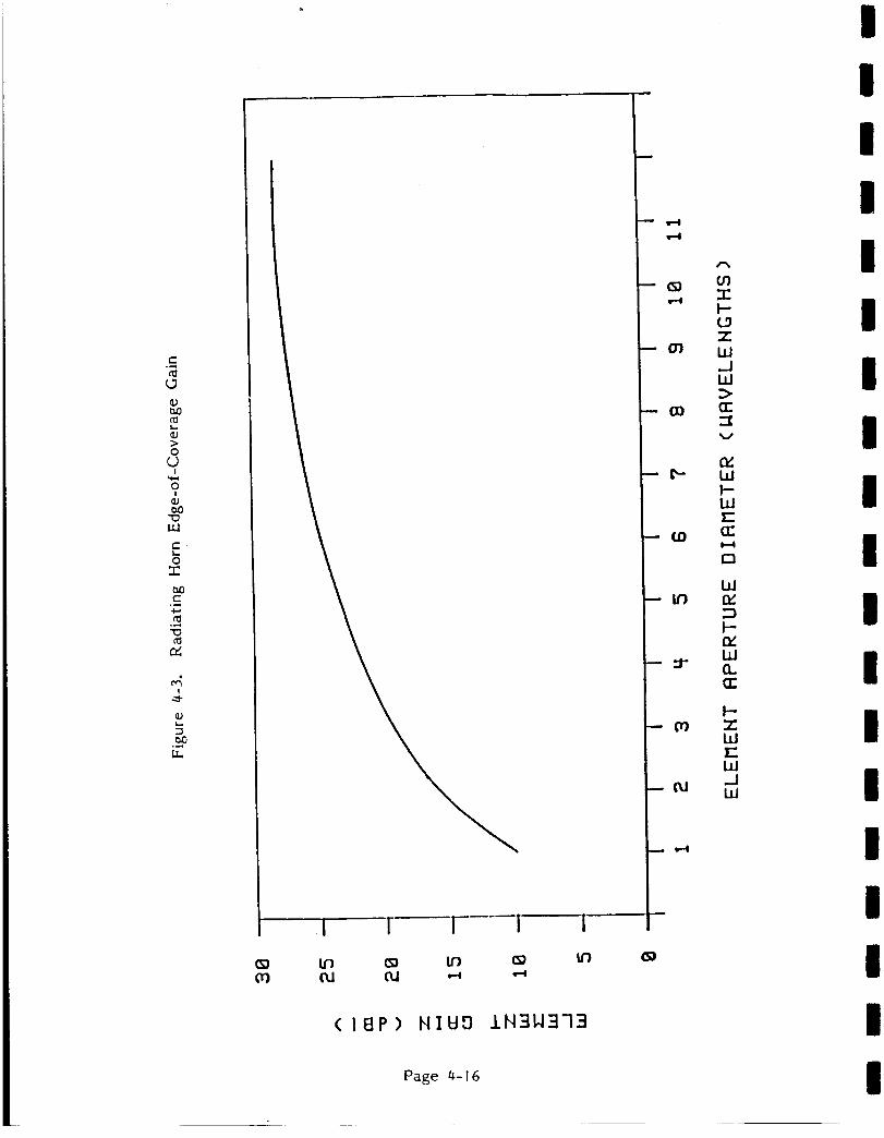
>0
I
0I
UJ
e--
8
I
fT.
I rWl I i
(18P) NIW5 1N3W373
Page 4-I 6
_(_1
I--
ZIJJ.JbJ
WI-WE
0
Wrv
l--n_WO.
I-ZWT-W.J111
l
II
lI
lI
I
II
I
III
I
II
II

I
II
II
II
I
II
I
III
II
II
Using (4-18), EIRP was calculated for different values of N, Pe, and D,
with maximum scan angle _ = 3.5". The results are shown in Table 4-2.
Note that the desired 0.9-deg beam coverage (i.e., 4.3-dB beamwidth) is
obtained with D --"46.4 in. instead of 56 in. as required by the array-fed
dual-reflector antenna. The difference in aperture size results principally
from the scan loss introduced by the dual-reflector system. The results
shown in Table 4-2 are plotted in Figure 4-4.
Radiation Patterns and Grating Lobes. The hexagonal active-aperture
array with 217 elements is shown in Figure 4-5. The diagram shows the
relative positions of the element centers; the element diameter is the
largest value permitted by the element spacing. Radiation patterns in the
plane of a major diagonal and in a plane bisecting an opposite pair of sides
can be calculated by reference to a linear array representing the hexagonal
array. In the first case, the off-diagonal elements in a direction normal to
the plane of the diagonal can be represented by a single-element radiator
with the appropriate excitation, as shown in Figure 4-5. The hexagonal
array can be represented by a different linear array to compute the
radiation pattern in a plane perpendicular to a pair of opposite sides.
An expression for the pattern E(8) in these planes is the product of
two terms, an element factor Geh(Q) and an array factor A(8). Exciting all
elements in the array with equal amplitude and a linear phase gradient to
scan the beam to the angle Ql, the radiation pattern in the diagonal plane
Page 4- 17

Table 4-2. EIRP for Active-Aperture Phased Array
Frequency = 19.7 GHz Wavelength= .598 Inches
Maximum Scan Angle= 3.5 Degrees
Array D_ameter = 58 inches Power per Element= .5 Watt********************** Beamwidth= .72 ***********************
Number of Diameter Loss Due EIRP
Element_ of Element To Element (Including all)(Inches) Factor(dB) Losses) (dBW)
91 5.273 -3.304 57.396
127 4.462 -2.319 59.825169 .3.867 -1.721 61.662
217 3.412 -1.330 63.137271 3.053 -1.059 64.372331 2.762 -0.863 65.435
397 2.522 -0.718 66.370
Array Diameter = 58 inches Power per Element= 1 Watt********************** Beamwldth= .72 ***********************
Number of Diameter Loss Due EIRP
Elements of Element To Element (Including all)(Inches) Factor(dB) Losses) (dBW)
91 5.273 -3.304 60.406127 4.462 -2.319 62.835
169 3.867 -1.721 64.672217 3.412 -1.330 66.148
271 3.053 -1.059 67.383331 2.762 -0.863 68.446
397 2.522 -0.718 69.380
Array Diameter = 52.2 inches Power per Element= .5 Watt
********************** Beamwidth= .8 ***********************Number of Diameter Loss Due EIRP
Elements of Element To Element (Including all)
(Inches} Factor(dB) Losses) (dBW}91 4.745 -2.640 57.144
127 4.015 -1.861 59.368
169 3.480 -1.385 61.083217 3.071 -i.072 62.480
271 2.747 -0.854 63.662331 2.486 -0.697 64.687
397 2.270 -0.580 65.593
Array Diameter = 52.2 inches Power per Element= 1 Watt
*********************** Beamwidth= .8 ***********************Number of Diameter Loss Due EIRP
Elements of Element To Element (Including all)
(Inches) Factor(dB) Losses) (dBW)91 4.745 -2.640 60.154
127 4.015 -1.861 62.378
169 3.480 -1.385 64.093217 3.071 -1.072 65.491
271 2.747 -0.854 66.672331 2.486 -0.697 67.697
397 2.270 -0.580 68.603
Page 4-I_
lII
II
II
ll
II
I
iII
II
II

I
i
I
!II
I
II
II
Ii
II
III
I
Table 4-2. EIRP for Active-Aperture Phased Array (continued)
Frequency = 19.7 GHz Wavelength= .598 InchesMaximum Scan Angle= 3.5 Degrees
Array Diameter = 46.4 inches Power per Element= .5 Watt
********************** Beamwidth= .9 ***********************Number of Diameter Loss Due EIRP
Elements of Element To Element {Including all)(Inches) Factor(dB} Losses) (dBW)
91 4.218 -2.062 56.699
127 3.569 -1.459 58.747169 3.093 -1.088 60.357217 2.729 -0.843 61.686
271 2.442 -0.673 62.820331 2.210 -0.549 63.811
397 2.017 -0.457 64.693
Array Diameter = 46.4 inches Power per Element= 1 Watt********************** Beamwldth= .9 ***********************
Number of Diameter Loss Due EIRP
Elements of Element To Element (Including all)(Inches) Factor(dB) Losses) (dBW)
91 4.218 -2.062 59.710127 3.569 -1.459 61.757
169 3.093 -1.088 63.367217 2.729 -0.843 64.696271 2.442 -0.673 65.831
331 2.210 -0.549 66.822
397 2.017 -0.457 67.703
Array Diameter = 40.6 inches********************** Beamwidth= 1.03
Number of
ElementsDiameter
of Element
(Inches )91 3.691
127 3.123169 2.707
217 2.388271 2.137
331 1.933397 1.765
Power per Element= .5 Watt***********************
Loss Due EIRP
To Element [Including all)Factor(dB) Losses) (dBW)
-1.563 56.038-1.109 57.937
-0.829 59.456-0.643 • 60.726-0.513 61.820
-0.419 62.781
-0.349 63.641
Array Diameter = 40.6 inches********************** Beamwidth= 1.03
Number of
Elements
91127
169217
271
331397
Power per Element= 1 Watt
***********************Diameter Loss Due EIRP
of Element To Element (Including all)(Inches) Factor[dB) Losses) [*BW)
3.691 -1.563 59.049
3.123 -1.109 60.9472.707 -0.829 62.466
2.388 -0.643 63.736
2.137 -0.513 64.8301.933 -0.419 65.7921.765 -0.349 66.651
Page _-19

Table 4-2. EIRP for Active-Aperture Phased Array (continued)
Frequency = 19.7 GHz Wavelength= .598 InchesMaximum Scan Angle= 3.5 Degrees
Array Diameter = 34.8 inches********************** Beamwidth = 1.2
Number of
Elements
91
127169
217
271331397
Power per Element= .5 Watt***********************
Diameter Loss Due EIRP
of Element To Element (Including all)(Inches) Factor(dB) Losses) (dSW)
3.164 -1.139 55.124
2.677 -0.810 56.897
2.320 -0.606 58.3392.047 -0.471 59.559
1.832 -0.376 60.6181.657 -0.307 61.554
1.513 -0.256 62.395
Array Diameter = 34.8 inches Power per Element= 1 Watt********************** Beamwidth= 1.2 ***********************
Number of Diameter Loss Due EIRP
Elements of Element To Element (Including all)(Inches) Factor(dB} Losses) (dBW)
91 3.164 -1.139 58.134
127 2.677 -0.810 59.907169 2.320 -0.606 61.350217 2.047 -0.471 62.570
271 1.832 -0.376 63.628331 1.657 -0.307 64.565
397 1.513 -0.256 65.405
Array Diameter = 29 inches Power per Element = .5 Watt
********************** Beamwidth= 1.44 ***********************Number of Diameter Loss Due EIRP
Elements of Element To Element (Including all)(Inches) Factor(dB) Losses) (dBW)
91 2.636 -0.786 53.894
127 2.231 -0.560 55.563169 1.933 -0.419 56.943
217 1.706 -0.326 58.120
271 1.526 -0.261 59.150331 1.381 -0.213 60.065
397 1.261 -0.178 60.890
Array Diameter = 29 inches********************** Beamwidth= 1.44
Number of
Elements
91127
169217
271
331397
Power per Element= 1 Watt
***********************Diameter Loss Due EIRP
of Element To Element (Including all)(Inches) Factor(dB) Losses) (dBW)
2.636 -0.786 56.904
2.231 -0.560 58.5741.933 -0.419 59.953
1.706 -0.326 61.1311.526 -0.261 62.160
1.381 -0.213 63.075
1.261 -0.178 63.900
I
I
I
I
I
r
I
I
J
I
I
I
I
I
I
I
Page 4-20

I
I
I
I
I
!
I
I
!
i
!
I
I
i
I
I
I
I
I
L_
5.*
<
cOc-OoOcOX_J
-i-
_uO
L_
n
i I I I I
_) In (_ In (S) in (:_
(MBP) 11BM J.d d_I3
I I I I I I I
O_ (S) CO _ :J" ('U
(SH10N373ABI1) _313HBIO /,B_dB
Page 4-21
CD
It')
cd
iiL
G) o)
v
I---0O.01
_ O
I--Qe
• ¢v
_J
Z

L.L.
t-o
t_x
0
E
>°-.,i
ILl
<
r"..,_
,--1
I
IJ
°_
0 o°
0 o°
0 o°0 o
000
000
000
0000 0
000
0 o
OF "POOR QUAI,,I'I"Y
)../r_,,
E
it.Ill
I--I
_.1
I--
II! ..uo-Jn"
n
•--s o+1:3 ,-Ill .-
¢h
u1
LT
0000
DO00
DO00
DO00
DO00
DO0 o0
DO 0
DO00
DO0 o
DO00
DO00
0 oDO00
0000
f'e
Iq
_P
141
p-
III
III
01
OI
III
III
m C
I0 0°.
OI
ill 0,,
R °.
m
sn hi
+
u o_
In
In
:IP
Illl
O
0
0
0
0
0
0
0
0
0
0
0
0
0
0
o-1Q
_+.+ +..,+,+_" _ _ .,"
_ .."
r_ .,._ W'
00/_Z 0
00000 0
0000 0 )_00 000
ez_O00oO 0 _-
000 n:_000000 i,_000 O0 ...jr=__. 111
0000 0 :z:-J00 00 o m
OoO 00 _
0000 0 _:P"0 0 O0 _x_u
000000 tu
0 o
Page _-22
I
I
I
I
I
I
I
I
I
I
I
I
I
I
I
I
I
I
I

II
III
I
II
II
II
II
II
II
I
is given by
Ed(e) : Geh(e)Ad(e) (4-19)
where Geh(e) is given by (4-9) with M -- 1 and _ = e, and
9
Ad(e) =9+_ aicos. ___[ill(do/_.)(sine-sinel )]
17
+ _-(18-i)cos [il_(do/1)(sin e-sin el)]i=l
(4-20)
where
a i = 8, i odd
a i = 9, i even
Note that a grating lobe occurs at eg when
Tl(dol_)(sineg-sin e I) = _+211 (4-21)
Solving for eg gives
sin eg = +_(2_./do) + sin e 1 (4-22)
The minus sign in (4-22) will be chosen, and e 1 will be assumed positive.
This combination, which places the grating lobe closest to the region of
interest (i.e., CONUS), yields
Page 4_23

sin eg = -[(2_/d o) - sin el] (4-23)
For the 217-elementactive-aperture array, do/)L= 4.66. Withe I = 3.5°,
eg = -21.7 °. The element pattern [see (4-9) with M=I] suppresses the
grating lobe 18 dB below the main-beam peak.
In the plane perpendicular to opposite sides of the hexagon,
E1(e) = Geh(e )Ap(e) (4-24)
where
8
Ap(6) = 17 + _: (17-i)cos [iT143(d0/_,)(sin e-sin el)]i=l
(4-25)
Note that a grating lobe occurs when
T_43(do/_,)(sin eg-sin 01 ) = +2_ (4-26)
Again choosing the minus sign,
sin eg = -[(2_L/_f3do)-sin t] 1] (4-27)
If the major diagonal is oriented to coincide with the maximum dimension
of CONUS, the maximum scan angle 81 in this case wit! be somewhat
smaller than 3.5", say 5.0 ° . The corresponding value of eg is -tI.3" The
grating lobe at this location is suppressed 13.8 dB.
Page 4- 24
I
I!
II
II
II
i
III
I
IiI
I
I

I
I
I
I
I
I
I
I
I
I
I
I
I
I
I
I
I
I
I
4.3. MBA With Beam Switching Matrix
Several traveling wave tube amplifiers (TWTA) operating at 20 GHz
have been developed for communication satellite systems. Of prime
interest are a series that have been space qualified, have 25-30W average
power output, and operate at approximately 33-percent efficiency.
Manufacturers of these TWTAs claim that 50-60W devices are within the
state-of-the-art. Use of these tubes in redundant systems, withswitched
beam antennas, has forced development of ferrite latching isolator
switches that have less than 0.I dB insertion loss and handle up to l OOW
average power. Existence of these devices stimulates consideration of the
transmit antenna subsystem schematically shown in. Figure 4-6.
Signals from the payload signal router are fed to four modulators
which are connected to any four of eight TWTAs. A redundancy switch
connects the selected four TWTAs to four MBAs. Each MBA has a beam
switching network that connects a single input port to any beam port. The
latter ports are connected to feed horns, each of which produces a beam
pointing to a different 0.9-deg spot within CONUS. Beams radiated by the
four MBAs provide contiguous coverage over a 7 ° x 3" field of view that
spans CONUS. Dual polarization characteristics of the horns and operation
at either of two frequency bands permit simultaneous excitation of four
beams on a noninterfering basis.
Antenna Configuration. The beams from the MBA provide coverage
over a 0.9-deg-diameter area, with the coverage areas forming the
triangular lattice structure illustrated in Figure 4-7. Minimum gain over
Page 4-25

X
i,.,
r-
r-U
V3
E
e-.
...,q
,<
I
-I
Page /)-26

III
II
II
II
II
II
II
I!
II
4.J
E
!
ZH
Page 4-27

the coverage area occurs at points equidistant from three adjacent beam
peaks. The beam-to-beam spacing is J3 x 0.45" = 0.78". A total of about
60 beams is required to cover the 7" x 3" area spanned by CONUS. A
representative 42-beam configuration is shown in Figure 4-8.
To maximize the gain of the MBA and minimize feed spillover losses,
four MBAs producing an interlaced set of beams are used. Each MBA
produces beams arranged in a hexagonal lattice, but with beam-to-beam
spacing equal to 2 x 0.78" = !.56". This permits the feed horns for each
MBA to be spaced farther apart then would be the case if a single MBA
were used. The greater spacing between feed horns permits use of
larger-aperture feed horns, thereby minimizing spillover losses. This
results in approximately 3-dB greater gain than could be obtained with a
single MBA.
The gain of an MBA beam can be expressed as
Gm = Tl(_O/_)218(J2(u)/u2)]2 (4-28]
where D is the MBA lens diameter, 11is approximately 0.6, and
u = (11D/_,)sine (4-29)
The angle 8 is measured from the beam peak to the observation point.
The lens diameter, D, is chosen to maximize the gain at the edge of
Page 4-28

IlI
lI
II
II
!I
II
I
III
lI
E
c/)>,
t-,t-
O
c-<0L=.
S..
t_I
L=.
0
t-.
t_
s..o
N
Et_
I
®
®
®
®
@
@
e
®
0
®
®
@
®
@
e
@
e
e
m_r-
/#
® e®.-. ®.-.®®.-. 0._0
t_ t_®,-. ®.-.®0.-. ®r.O®._ ®.-.0®.-, ®.-.®
Oc_O .-.®.-. L_®@®®®
®
# ®
m ®5--
®
S
_0
@m
_- ®
0
O
0
O
®
®
®
O
@
0
O
G
®
®
0
®
Page #-29

the beam coverage area (i.e., 0 = 0.45"). As with the previously discussed
antennas, the 4.3-dB beamwidth is 0.9". The lens diameter is then
determined by taking the ratio of the gain at the beam peak to the gain at e
= 0.45"_
10 log [Gm(O" )/Gin(.45" )] = 10 log [8(J2(u.45. )/u2.45, )]-2
= 4.3 dB (4-30)
where u.45. is the value of u at e = 0.45". Solving this equation for u.45,
results in
u.45. -- (_D/_.)sin (.45") = 2.36 (4-31 )
Finally, D is determined to be 56.6. in. and the gain at the edge of the
coverage area is 43.0 dBi.
Assuming a loss of 1.5 dB in the RF switch network between the
transmitter and the MBA feed horns, a transmitter output power of i OOW
will produce an EIRP _ 61.5 dB over a beam coverage area 0.9" in diameter.
Switch Network. The switching design considered for use both in the
MBA beam-selection circuitsand the TWTA 8x4 redundancy switch is a
ferrite circulatorswitch configuration. This type of switch has been
space-qualified for satelliteapplications in the 20-GHz downlink band.
These switches have demonstrated low insertion loss and the abilityto
handle relativelyhigh (~100W) levels of RF power. The switching speed
Page 4-30
II
I
I
I
!
I
II
I
I
II
II
I
I
I
I

I
I
I
I
I
I
I
I
I
i
I
I
I
I
I
I
I
I
I
depends on the amplitude of the voltage pulse applied to the circulator's
ferrite-core drive wire within the switch. For a given ferrite switch,
doubling the applied voltage will approximately halve the switching time.
Other parameters governing switch speed are the coercive force,
hysteresis properties, and the mass of the ferrite used in the switch.
A switch operating in the 20-GHz band requires about 7.54 iljoule for
switching. To switch in I00 ns, a 75-volt drive pulse is required. The
switch driver that produces this pulse can be expected to operate at about
15-percent efficiency, so the switching energy required is about 50 Iljoule
per switch per switching event. Thus a single switch, switching at 20K
events/sec, requires about one watt of driver power.
The 8x4 redundancy switch shown in Figure 4-6 requires 52 ferrite
switches, with a maximum of 5 switches in series between any TWTA and
the input to any MBA beam-selection switch network. The beam selection
networks require a total of 38 switches, with a maximum of 4 switches in
series between the input and any MBA feed horn. With 0.I dB insertion loss
per switch, and assuming 0.5 dB for the net loss of the interconnecting
waveguide, the total switch network loss is 1.4 dB, as previously
suggested.
Although the total number of switches required is 94, it can be
asasumed that the switches making up the 8x4 redundancy switch are
rarely, if ever, switched. In addition, to switch beams in the
beam-selection networks, a maximum of four switches in any network
Page 4-31

need be switched. A four-beam system will therefore require that no more
than 16, and usually only about eight, switches be switched to shift all
four beams. Thus, the maximum beam switching power for shifting four
beams at a 20K/sec switching rate is about 16W.
4.4. Comparison of Antenna Configurations
To achieve a specified performance level, the active-aperture phased
array and the array-fed dual reflector antenna require a similar number of
radiating elements. The former has the advantage of not suffering scan
loss. It also has better polarization purity in a dual-polarized system.
However, the direct-radiating array has a linear dimension that is larger
than the array dimension in a dual-reflector system by nearly the
magnification factor, M. Typically, M=3. Thus, the dual-reflector system
has the advantage of more convenient array packaging and perhaps more
conventional deployment. The two systems have comparable weight and
power requirements.
The MBA, on the other hand, requires considerably less power than
either of the other two configurations, because of the higher efficiency of
TWTAs as compared with SSPAs. It is estimated that this power ratio is
in the range of 50 to 60 percent. Aside from the need to develop a I OOW
TWTA at 20 GHz, however, the MBA approach suffers from the vulnerability
of the system to TWTA or beam-switching network failures. While TWTA
redundancy can ameliorate this vulnerability, reliable data on TWTA
lifetime is difficult to obtain. By comparison, both phased-array
approaches can tolerate a number of SSPA failures before system
Page 4-:32
III
I
III
I
II
II
II
III
II

I
I
I
I
I
I
l
l
l
I
I
I
I
I
I
I
I
l
I
performance is noticeably affected. This graceful degradation greatly
enchances the attractiveness of the phased array configurations.
The MBA configuration also suffers from an aprior/ partitioning of
geographic coverage, as illustrated by the feed-horn assignments in Figure
4-8. If the traffic should not divide evenly among the four composite
geographic areas, saturation of a single downlink beam would lead to
degraded service at a total throughpu t which is less than the nominal
satellite capacity.
Because of the large number of elements involved, realization of
either phased array configuration at reasonable cost depends on advances
in monolithic microwave integrated circuit (MMIC) technology. The
desirable degree of integration (e.g., combined vs. separate modules for
each phase-shifter/amplifier pair) remains to be determined.
Page 4-3:3

II
IH
II
e
III
a
II
IB
II
BI
5. BULK DEMODULATOR TECHNOLOGY
The bulk demodulator units provide FDM/PSK-to-TDM digital
conversion and measure both signal amplitude and phase on over iO0
individualtone slots. The signalphase is differentiallydetected to form
the user data stream, while the signalamplitude is used during acquisition
for timing alignment. Both analog (SAW) and digital (FFT) bulk
demodulator techniques are examined, together with digitaldata detection
and post processing requirements.
Uplink symbol transitionsforeach FDMIPSK channel are synchronized
to the onboard bulk demodulator timing. This allows a factor-of-3
reduction in the number of Fouriertransforms required and eliminates the
need for data interpolation. If the terminals were allowed to be
nonsynchronous with the demodulators, many of the symbol start/stop
times would overlap transform boundaries and cause intersymbol
interference,as well as a loss indetected energy due to a time mismatch
in the detection filter. This time synchronization requirement is much
less stringent than for TDMA systems such as ACTS, where the terminals
must meet 25-ns accuracy. The accuracy requirement for the present
system is about 1 ps.
Intermodulation and adjacent-channel components are also a concern
with the FDM/PSK multiple-carrier format. With the SAW demodulator,
sufficient dynamic range must be provided to avoid nonlinear mixing
effects. In the FFT, the A/D and arithmetic quantization must be fine
enough to ensure accurate reconstruction of the signal, while the range
Page 5- !

must be wide enough to ensure that arithmetic overflow does not occur.
Since the transmit levels of the terminals in any uplink spot beam will be
approximately the same, the dynamic range can be limited to the number of
terminals multiplied by the signal-to-noise ratio for a single terminal.
With 100 channels and a received Eb/No of 15 dB, the quantization range
must be at least 35 dB. This requirement is easily met with an 8- to
10-bit A/D converter.
5.1. SAW Demodulators
One form of FDM/PSK demodulation uses surface acoustic wave (SAW)
devices to implement an analog spectrum analyzer known as a chirp
Fourier transform. Use of SAW demodulation for spaceborne
communications was first investigated by MIT Lincoln Laboratory for the
FEP EHF package on FLTSATs 7 and 8. Development of the SAW demodulator
at TRW has further refined the technology to meet the additional
capability and reliability required for MILSTAR. This effort has
demonstrated the ability to manufacture large numbers of these SAW
devices, as well as mechanical mounting and digital temperature
compensation techniques for both normal and stressed spacecraft
environments. The SAW demodulator typically requires from one-third to
one-fourth the power required by conventional LSl-based digital FFT
processors.
The SAW demodulator examined in this study consists of three basic
components: the Fourier transformer, a digital section, and a common LO
section (Figure 5-I). In this particular implementation, there are eight
Fourier transformer and eight digital sections for each common LO section.
Page 5- 2
I
I
II
I
I
II
II
I
II
II
III
I

Page 5-3

Each demodulator path is responsible for demodulating 100 uplink user
channels, while the common L0 section supplies a chirp LO and digital
timing signals to each path. This LO sharing greatly reduces the overall
parts count and power, but still allows for graceful degradation in the
event of common LO failure. These components will be described in
greater detail in the following sections.
The Fourier transformer can be implemented in two generic forms:
convolve-multiply-convolve (CMC) and multiply-convolve-multiply (MCM).
These two transforms are mathematical duals of each other and, in theory,
produce the same results. The CMC transform, pictured in Figure 5-1,
provides additional input filtering and uses a single chirp LO generator,
thereby eliminating some of the temperature-controlled timing alignment
required in the MCM approach to hold phase stability.
SAW Fourier Transformer. A SAW Fourier transformer block diagram
is shown in Figure 5-2. The Fourier transform sections use devices known
as reflective array compressors (RAC), shown in Figure 5-3, to implement
dispersive time delay functions. The dispersive delays cause tow
frequencies in their bandwidths to be delayed longer than high-frequency
signals. Through use of RAC devices, linear FM chirps can be compressed
to a single pulse.
The Fourier transform section first passes the input signals through a
dispersive delay to offset their time positions and then mixes them with a
linear FM chirp from the common LO section. The mixing is done in a
bilinear mixer, which is implemented as a high-frequency analog
Page 5- 4
I
I
II
II
I
I
II
II
II
II
!I
I

l
i
I
l
i
I
g Page 5-]

c-O
°.-0
r_0
<
r_
E0U
I.
<
.-,t×
r_
I.
lao-4
I
I
_ I-_- I
Page 5-6
I
I
I
I

I
I
I
I
I
I
I
I
I
I
I
I
I
I
I
I
I
I
I
multiplier to avoid intermodulation products. The result is a series of FM
chirps, one for each input signal, which cover the same sweep range but
overlap in time. Another RAC device, used as a chirp compressor, converts
these time-overlapped chirps into discrete time pulses, each
corresponding to a different input signal. The amplitude of each pulse
envelope and the phase of the carrier under the envelope depend on the
input signal amplitude and phase. The time position of each pulse is
proportional to the input signal frequency. Figure 5-4 shows the accuracy
of the reconstructed signal phase.
The output pulses from the Fourier transform section are routed to
the digital .section through a SAW bandpass windowing filter. Since the
SAW demodulator is a true Fourier transformer, input frequency is
translated to output time, and input time is translated to output
frequency. In particular, input-time offsets due to terminal timing
misalignment result in changes in carrier frequency under the pulse
envelope. Providing a filter characteristic in the frequency domain at the
output of the SAW Fourier transformer is equivalent, therefore, to time
windowing at the demodulator input. Windowing is desirable for reduction
of sidelobes caused by close adjacent-channel spacing.
The windowed pulses are passed through a limiter and a quadrature
phase detector. This removes any amplitude variations and produces
inphase and quadrature phase components which can be sampled and
processed by the subsequent digital circuitry. In addition, a linear power
detector is used to extract a measure of signal power for use in terminal
acquisition and temperature compensation.
Page 5- 7

"r"
c-.
o
c.-o¢)
<u
o
0
_J
t.,
o
..coL)
"T"
I
oD
L_
'POOR QUALITY
Page 5-8
I
I
I
II
I
I
I

II
III
I
II
II
II
II
III
II
SAW Common LO. The common LO section provides the linear FM chirp
signal to each of the Fourier transform sections. The chirps are generated
by RAC devices which are sourced by an RF pulse generator. The pulses,
which consist of a few cycles of a high frequency LO (typically 200 MHz),
can be thought of as wideband (sin x)/x shaped bursts in the frequency
domain, with the sinc center at the LO frequency. The RAC devices delay
the low-frequency components of this signal by a greater amount than the
high-frequency components. This results in a chirp signal that shifts from
high to low frequency for each pulse input. The time positions of the input
signals at the Fourier transform mixer requires the generation of chirps at
a rate of one per input symbol and with a duration of almost two symbols.
This means that there are, in general, two different chirps simultaneously
present at the output of the chirp generator. The existence of two chirps
in the mixer LO port is the driving factor in the selection of a bilinear
mixer. Use of a conventional double-balanced RF mixer would result in
intolerably large intermodulation products.
Also located in the common LO section are the calibration tones and
the temperature compensation loop controller, which are used in
correcting demodulator temperature variations. The controller can be
shared among the eight Fourier transform sections and is described
further in the digital section.
Digital Section. The digital section input consists of a phase
quantizer, which performs quantizations based on a ratiometric
comparison of the I and Q inputs, and a sample/hold amplifier followed by
a low-speed, high-accuracy A/D converter, which can quantize the power
Page 5- 9

detector output for selected channels. The clock signals
quantizers are generated by a digital temperature tracking loop.
for the
Temperature compensation is necessary in SAWdemodulators because
the surface wave propagation velocity in the RAC devices changes as a
function of temperature. This causes the output pulses to vary position in
an accordian-like fashion, getting closer together or farther apart.
Careful design of the SAW demodulator transform relationships ensures
that this variation never causes one transformed time output to overlap
another.
Accurate sampling of a particular" set of frequencies, however,
requires a tracking loop that follows any changes in output time position
and corrects the quantizer sampling frequency and phase accordingly. The
tracking loop required in this application is quite similar to the loop
developed for MILSTAR. Calibration tones are injected by the common LO
section into eachFourier transformer, one at a time. The calibration tone
frequencies are well outside the portion of the input bandwidth used for
communications and are injected at the bilinear mixer. This produces an
output pulse that provides a reference time position for the band.
Switching between the lower and upper bandedges allows the temperature
compensation loop to track the time-offset and scale-factor variations
caused by temperature. A numerically controlled oscillator (NCO)in each
digital section provides a sampling which can be adjusted in both phase
and frequency to match that demodulator's characteristics.
The remainder of the digital section is devoted to data detection.
Page5- 10
I
II
III
II
I
II
II
I
I
I
I
I
I

II
II
II
II
II
II
II
II
II
I
QPSK data detection is performed by subtracting the phase measurements
of two adjacent symbols and comparing the result to one of four possible
90-degree phase shifts. The closest match is selected as the received
symbol and is passed to the downlink multiplexer. This differential
detection scheme provides carrier frecluency independence at the expense
of a doubling in BER. The resulting simplification in the terminal and
satellite hardware is considerable since no carrier phase coherence is
required.
SAW Bulk Demodulator Technology. SAW demodulators are currently
being manufactured for the MILSTAR program. These units have a slightly
different LO sparing arrangement, but use the same technologies.
Technologies developed at this point include: SAW RAC devices and
mounting techniques for 6-inch crystals, wideband bilinear mixers, SAW
window filters, log amplifiers, and a high-speed phase quantizer. The
temperature compensation hardware uses custom integrated circuits for
implementing the digital tracking loop and control functions.
Most of this technology is usable in its present form. However, new
RAC devices are required for a different application. In addition, a new
temperature control IC and microprocessor control algorithm are required.
Total power consumption for a current-generation unit is about 15W per
demodulation path, or 1500W for I00 demodulators. Significant
reductions in RF power required for the SAWs and the bilinear mixer are
not expected, but further reductions in sampler
power may reduce the power per demodulator to
demodulator is estimated to be 5 lb.
and control hardware
10W. The weight per
Page 5- 1 I

5.2. FFT Demodulators
The FFT is an efficient implementation of the discrete Fourier
transform (DFT) in cases where a large number of orthogonally spaced
channels must be separated. The FFT is an all-digital implementation and
thus can be much lower in manufacturing cost than SAW techniques. In
addition, immunity to temperature .and aging effects make the FFT
desirable if low-power operation can be obtained. In this case, a
128-point FFT with 2:1 presumming is used to separate 100 channels at
approximately lO0-kHz spacing. The remaining 28 transform slots fall
into the roll-off of the input filter, which is used to prevent aliased
components of other channels from entering the desired l O0-channel
group.
An N-point FFT requires (N/2) log2N complex multiplications. For a
128-point FFT, this results in 448 complex multiplications. Since the
baud rate is roughly 50 kHz, with one FFT required per baud, the
computational requirement is 22.4 million complex operations per second
(22.4 MCOPS). Two different architectures can be used to perform these
operations, a recursive FFT and a pipelined FFT.
Recursive FFT. The recursive FFT, as its name implies, performs FFTs
using a single arithmetic element by recursively performing the algorithm
Since the FFT algorithm is regular in structure, it can be separated into
log 2 N passes of length N/2. An example of a chip set which currently
implements such a recursive FFT is the VHSIC Phase 1 FFT chip set, shown
in Figure 5-5 This TRW-developed chip set, which performs FFTs of
Page 5- 12
I
I
I
I
I
II
II
II
II
II
II
II

variable length at rates up to 8.2 MCOPS, consists of a arithmetic unit, a
control unit, and several four-port memories. By the previously determined
sizing, three such sets would be required to perform the transform in the
required time. Actually, introduction of presumming and trigonometric
recombination functions (described later) make the need for a fourth chip
set probable.
Two members of the chip set have completed fabrication and initial
test. Current estimates are that the complete set will be available in
1987 and will consume approximately 2.5W of power. The total power
requirement for just the FFT portion is thus about 10W. Addition of the
A/D converter, buffering and control circuitry puts the total power at
approximately 12.5W.
Current-generation VHSIC Phase 1 FFT chips are radiation hardened
only to about 104 rad/Si, which is insufficient for most geosynchronous
requirements. Future generations of these chips, built in the radiation
hardened 2-1Lm CMOS process used for MILSTAR, should have radiation
hardening to 3x10⁵ rad/Si and should also require less power The
projected total power requirement for a CMOS recursive FFT design is
about 9.5 W. The corresponding weight is estimated to be 3.5 lb.
Pipelined FFT. The pipelined FFT performs the same algorithm as the
recursive FFT, but it uses a cascade of high-speed stages to perform
successive passes of the algorithm in separate arithmetic units. This
procedure allows the input of the FFT to operate synchronously with
Page 5- 13

Q..
_D
[.-.[..T.IT.
:>
t.,
L.T.
Page 5-1 4

II
Il
II
I
II
II
II
I
III
II
the A/D sampling, thereby eliminating multirate clock difficulties often
encountered in recursive algorithms. In addition, the parallel (rather than
serial) processing eliminates the need to switch between processors at
each baud.
Figure 5-6 shows the architecture of a pipelined FFT developed at
TRW. The architecture is based on a complex multiplier, a radix-8 DFT
element, and a 64-sample intermediate memory. Each set of these
components can perform the equivalent of 15 MCOPS. Three sets are
required to perform the necessary calculations for a radix-128 FFT
(radix-8 x radix-8 x radix-2). These three sets can readily perform the
22.4 MCOPS previously established as the FFT requirement. These chips
require approximately 1.8W per set. They are currently manufactured in
the 2-1_m CMOS process, with some amount of additional processing needed
to produce radiation hardened devices. Total power for a pipeline design is
about 8.5W. Each unit weighs about 3.2 lb.
Real vs. Complex Sampling. Another issue for FFT-based demodulators
is the question of real versus complex sampling. In most textbooks, FFTs
are shown with complex input samples and complex results. This
arrangement eases understanding of the algorithms, but it often is not
practical to implement. For the present application, which involves
spectrum analysis, a high degree of phase and amplitude matching between
the quadrature input samples is required to eliminate introduction of
in-band al iasing.
As depicted in Figure 5-7, the complex-sample FFT relies on accurate
Page 5- 15

E
1.1.
rn
v(3
_orn
,el.,I.l.,
I.,
I..I.,
Page 5-1 6

II
II
II
I
II
II
III
II
II
I
E
c_
E
4J
.C:
O4-J
Qu'1
_J
E
oL.
I-=-
l=IdZC_Q..
l=IJ
..,..a.
Z
c",4
I--.
__JIdd
Z
I-..-
IJ.JId=.
I=I=Ia.
m
I"--
LEt
1.4.4
m
3I
<I+_
s...-
3
C:)
b,_ c',J
Page 5-1 7
,3
I"-
uJ
l,w
I---
CI
I
<'1+
c',,4 _
,3
I

cancellation of image frequency components. If the quadrature
downconversion process is unbalanced, these image components leak
through. This effect is especially degrading where the dynamic range
between users is high, since the image of a strong user can completely
mask a smaller user signal. A plot of image strength versus phase and
amplitude offset is shown in Figure 5-8. In this case, accuracies of better
than 0.5 dB and 2 degrees are required for adequate performance. These
tolerances, which are extremely difficult to maintain over temperature
and satellite aging, result in high design, component and assembly costs.
One technique for eliminating the effect of quadrature sampling
imbalance is to use real sampling. This requires that the input be
downconverted to a (low) frequency offset from baseband. The input is
then sampled by a single A/D converter operating at a rate equal to twice
the input bandwidth. Although the A/D speed is twice that of the complex-
sample case, only one converter is required. In addition, since there is
only one path, there is no concern for amplitude or phase matching with
this design.
Real sampling requires that input samples be fed only to the
real-component input of the FFT. With the same number of samples per
baud as complex sampling (half the number of samplers at twice the rate),
real sampling normally requires an FFT which is twice the size used for
complex sampling. In the present case, a 256-point FFT would be required.
This is feasible with both implementation approaches, but requires
additional hardware in the recursive design. The pipeline design shown
has sufficient speed capability to handle a 256-point FFT with the same
Page 5- 18
I
I
I
I
I
I
I
I
I
I
I
I
I
I
I
I
I
I
I

II
I
II
lI
II
II
II
II
II
II
Figure 5-8.
1.8
1.6
1.4
1.2v
ILl
¢.==3
z 1.0
IDa
-- 0.8
==_i-==.=====Io_ 0.6
0.4
0.2
00 °
Effect of Amplitude and Phase Mismatchon Signal-to-Image Ratio (SIR)
Sift = 20 dR
SIR = 25 dB
SIR -- 30 dB
= 35 dB
SIR = 40 dB
SIR = 45 rib
t) Oz....
I I
4° 6° 8°
PI4ASEERRQR(DEGREES)
10° 12°
Page 5-I 9

hardware. The memory size must be increased, however, to accommodate
the larger number of transform points_
To avoid a factor-of-two growth in the recursive FFT architecture, a
technique called the trigonometric recombination algorithm was
developed. This algorithm allows every other sample of a real-sample
input to be placed in the I and Q inputs of the FFT. The in-phase and
quadrature components are transformed and, because of their orthogonal
input relationship, can be recovered at the output. An additional
algorithmic pass is required to combine image frequency components to
produce the desired result. Besides slowing the input rate seen by the FFT
by a factor of two, this procedure allows the" computations (and thus the
hardware) required to be reduced by a factor of two as well. The total
computational effort is approximately 14 percent greater than that
associated with a complex-input FFT.
Presumming. Since the FFT provides output samples at orthogonal
spacing (in this case about 50 kHz), while bi-orthogonal carrier spacing
(100 kHz) is used on the uplink, there are twice as many output values as
needed. This computational inefficiency can be reduced through a process
known as presumming. Figure 5-9 shows an 8-point FFT example.
If only the even-numbered channels are required at the output,
approximately one-half the computations can be eliminated by performing
only the additions (multiplication by WO) in the first FFT pass and then
implementing a 4-point FFT for the remaining passes. In the present case,
only 12B of 256 orthogonal positions are needed. Instead of implementing
Page 5- 20
I
II
III
II
I
II
I
I
i
I
I
I
I
I

I
I
u.f'_
I
II
IiI _
III
I!
iILl
l Page 5-21

a 256-point transform, a 128-point transform with 2:1 presumming is
performed.
The presumming consists of storing the first-128 sample points
(complex) and then adding them one-by-one to the remaining 128 sample
points. This produces the 128 complex points which are the even
components of the first pass of a 256-point transform. A 128-point FFT
is then performed to yield the required results. This technique is
mathematically identical to the 256-point FFT and can be used to reduce
both the effective input sample rate and the FFT size required.
5.3. Conclusions
In terms of current technology, the SAW demodulator represents the
only technique which is both radiation hardened and currently undergoing
space qualification. Compared to current qualified discrete LSI
techniques, the SAW demodulator holds a favorable position for wideband,
low-power Fourier transforms. However, evolution of digital FFT
algorithms and LSI processes makes it quite likely that the eventual
choice for this application will be an FFT. Insensitivity to temperature
effects, constant high precision, lower power and reduced manufacturing
costs make FFTs an attractive alternative to SAW demodulators for future
applications.
Page 5- 22

I!
I
II
II
I
III
II
II
I
II!
6. BASEBAND MULTIPLEXER TECHNOLOGY
The baseband multiplexer is responsible for assigning uplink
frequency channels to downlink time slots in a fashion which allows
programmable interconnection of terminals and efficient use of both
uplink spectrum and downlink data fields. A large number of serial
streams (representing the bulk demodulator outputs) must be multiplexed
into a small number of high-rate downlink streams with selectable paths
corresponding to particular downlink-beam dwells.
The requirements governing the multiplexer implementation trades
are summarized in Table 6-I. The number of multiplexer inputs
corresponds to the complement of I00 demodulators, each of IO-MHz
bandwidth. A nominal 100-kHz channel spacing has been selected for the
multiplexer analysis; consequently, there are I00 channels per
demodulator. The channel data rate of 413 x 64 = 85.3 kbps (which
includes the effect of rate-314 coding) has been rounded up to 100 kbps.
Consequently, the multiplexer inputdata rate is 10 Mbps per demodulator.
The corresponding multiplexer throughput is I Gbps. (Note that, when
rate-314 coding is appliedto the satellitethroughput of 790 Mbps, a coded
data rate of 960 Mbps results.)
It is assumed for descriptive purposes that the multiplexer must
simultaneously process one quadriphase symbol per channel for each of
10,000 channels. (Itwas pointed out in Section 2 that multiple symbols
Page 6- I

+.J
E
o"
X
{2.o_+.J
uc_
I
!
O
G_r-
= I
Page 6-2

II
!
II
IIIi
II
lI
II
II
II
per channel must be processed jointly to limit the scan rate of the
downlink beams.) Six downlink beams are assumed for purposes of this
analysis. (The baseline system has four downlink beams.) There are
therefore 10,00016 = 1666 time slots per scan for each beam, under the
simplifying assumption that the two bits in each quadriphase symbol have
a common destination. The output data rate per beam has been rounded up
from 166 Mbps to 180 Mbps to account for the effects of overhead and
beam-switching intervals.
Three different multiplexing techniques were evaluated. Each was
selected based on its particular merits in one or more categories: size,
power, interconnection flexibility, and terminal constraints.
6.I. High-Speed SerialTime-Domain Multiplexers
A logicalfirststep in any multiplexer study isto consider the use of
standard, serial multiplexing techniques. Because of their serial nature,
these multiplexers are often small and easily understood. In this
application,however, serialmultiplexers are at a disadvantage. The high
rate of information flow, I Gbps, limits the abilityof serialmultiplexers
by requiring high-speed IC technologies which currently do not support a
high degree of integration. In addition,these multiplexers are often best
designed for single output applications where significant time
rearrangement is not necessary. In this application,not only must signals
be switched among several outputs,but they must also be rearranged in
time sequence to allow connection of any uplink frequency slot to any
downlink dwell.
Page 6- 3

The speed issue can be ameliorated by using a separate multiplexer
for each downlink. This lowers the maximum speed to about 170 Mbps and
eliminates many of the elastic buffering requirements which might appear
with several downlinks vying for the same multiplexer output. To
facilitate time reordering of symbols between bulk demodulator and
down]ink beam, each demodulator is provided with a 200-bit buffer
memory (one quadriphase symbol for each of 100 channels) which is
written in a random order and then read sequentially for downlink
transmission. The configuration of random write and sequential read
(rather than the reverse) is chosen to minimize speed requirements during
downlink readout, where successive reads may be spaced by as little as 6
ns. (Interleaving addresses on smaller memories could reduce the speed
requirements further, but at the expense of large numbers of extremely
small memories.)
With a single 200-bit buffer assigned to each demodulator, the
possibility exists that two or more downlinks may require symbols to be
read from a commonbuffer memory for transmission during the same time
slot. This memory contention problem can be avoided by providing a
separate buffer memory for each demodulator/downlink pair. The most
logical configuration would be a set of six addressable shift registers, as
shown in Figure 6-1. These could be integrated on the same chip and
fabricated in a high-speed bipolar process.
Page 6- 4
II
!
II
I
IIi
II
!
Ii!
II
I
I

!
II
I
!
!
I
!
I
I
I
!
I
I
I
!
l
ORIG:?:AL P_ ;3
OF POOR QUALITY
_'_
5.,
x_J
Q..4.a
-I
c-
E0Q
E[.-
c-
OE
-s
[I _004 U
_'_
@
eL.
£
S,,0
£I1
TToooTX "_ _
m
=EO0E_
--4G'-
_0_
t)X
Z:
• ,X=
m
=3
0
_J
L0
0
I
i Page 6-5

Combining of demodulator outputs can be done in either a serial chip
interconnectionscheme, shown in Figure 6-2, or a parallel multiplexing
scheme, as shown in Figure 6-3. The serial scheme requires fewer
interconnections,but requires relay cross-strapping of the serialchain at
regular intervalsto avoid single-pointfailures.
6.2. Frequency-Domain Multiplexers
A simple technique for reducing on-board multiplexing requirements
isto arrange the uplink frequency slots in a manner that allows simple and
efficient direction to the downlink. Reassignment of multiplexed
interconnections is performed by reassignment of uplink frequencies and
downlink time slots.This results in minimum on-board processing, but it
puts some limitationson interconnectionflexibility.
Figure 6-4 shows an uplink frequency assignment plan for an
approximately 80-MHz segment (one-sixth) of the 500-MHz uplink band.
The plan is designed for a satellite system with six independent downlink
scanning beams (labeled A through F). This frequency plan is arranged so
that each sixth frequency slot is assigned to the same downlink beam.
This allows simple uplink spectrum reorganization by downlink beam. It
also helps reduce multiplexer speed requirements, since similarly lettered
bits from each demodulator can be passed in parallel to a common buffer
and converted to serial form for high-rate downlink transmission.
Furthermore, adjacent 80-MHz uplink segments have their A to F
downlink beam assignments rotated by one position, thereby ensuring that
Page 6- 6
I
I
I
I
I
I
I
I
I
I
I
I
I
I
I
I
I
I
I

0°_
U01-"t-OUI.
c-i.-i
._
0X0
I::L
r-
E
o
i
EE--
i1)
U.
0 0
_8
_ 0
o_
tttttl
lttt÷_IIIII
]
_ IIIIII
" lltltTw
Illll/
tllllt
Page 6-7
ORIG;?;PJ. PA,.%.Z ""
OF POOR QUALITY
Mo,,=;U
3
og
-i

0
t-
o
c-
c_
n.
x
+_
r,°_
E0
EF-
i
U.
111111
-:i-_o
IIIIII
3
O
'_ IIIII1
fo
IIIIII
IIII11
I
i
!
_2IIIIII _
Page 6-8
I!II
!
III
II
I
I
Ii
I
I
I
II

!
ORIGIi_IAL PA,_ I_OF POOR QUALITY
-7
.a_2. ._
I-
Page 6-9

symbols transmitted simultaneously on the six beams are drawn from
different 80-MHz segments. A particular downlink beam, say A, is fed
data from the lowest 80-MHz segment (on both polarizations) during the
first uplink symbol interval. It is fed data from the second segment during
the next uplink symbol interval, and so on until all six segments have been
read. At this point, the downlink multiplexer returns to the first 80-MHz
segment and the sequence is repeated.
Approximately 16 demodulators are read in each position, eight from
each uplink polarization. As the A multiplexer moves to the demodulators
that correspond to the second 80-MHz segment, the B multiplexer moves to
the first 80-MHz segment to receive symbols from the B-designated
frequency slots. In this manner, a continuous flow of data is maintained
and the word transfer rate does not exceed I0 MHz, allowing CMOS
technology to be used for low power consumption.
The description thus far has focused on the association of uplink
frequency channels with particular downlink beams. The nature of the
traffic matrix supported by such a multiplexing scheme is also illustrated
in Figure 6-4. On the uplink, a specific set of demodulators supports each
regional beam. One-sixth of the composite capacity of these demodulators
is directed at each downlink. Within any frequency subset (corresponding,
for example, to letter A), the fractional number of channels allocated to
(say) New York-directed traffic must correspond to the percentage of time
the downlink beam dwells on New York. This is true for every uplink
region.
Page 6- 10

I
I
I
II
I
I
I
!
I
I
I
I
I
I
tI
II
I
Whether this constraint on the allocation of satellite capacity
significantly decreases the traffic throughput depends largely on the
number of uplink regions. The effect on throughput will be relatively
small ifthe number of uplinkregions is small. (Note that there are eight
uplink regions in the baseline system.) However, ifa single metropolitan
area (such as New York) dominates a region,the percentage of trafficfrom
that region to the metropolitan area may be significantlyless than the
percentage of trafficfrom other regions to that metropolitan area. In this
case, the corresponding satellitecapacity will be unclerutilized.
A further shortcoming of thismultiplexing scheme is that continuous
transmission on some channels may have to be interrupted for short
intervals during reallocation of satellitecapacity. This is a drawback
when compared to a truly random assignment multiplexer,but it is not a
severe constraint if only short-duration data/voice connections are
required.
6.3. Memory-Based Multiplexers
Memory-based multiplexing techniques are gaining increasing favor
because of the tremendous flexibility that they offer (random
interconnect).Memory technology is also a rapidly developing area, with
increased size,faster speed, and lower-power units being introduced at a
quickening pace. Current concerns with spaceborne memory devices center
on radiation hardness and single event upset (SEU). Many current CMOS
memory devices are showing satisfactoryhardness (IE5 radlSi) for space
environments, but they are limited to about lO0-ns access times.
Page 6- I1

SEU-induced bit flips do not represent a significant problem for this
application, because they show up as random bit errors which are
corrected by the end-to-end coding. SEU latchup remains a critical
concern in device selection. Current generation, hardened memories are
designed to be latchup-immune through use of dielectric isolation,
epitaxial processes, or similar techniques.
Memory-based multiplexers range in size and complexity from simple
address-pointer techniques to time-space-time techniques similar to
those found in telephone switching systems. The address-pointer
technique is shown in Figure 6-5. This is a modification of the serial
multiplexing technique. However, in this case each demodulator has a
memory which can hold up to 2 x 104 bits of data. This memory capacity
represents one data symbol for each downlink-beam/time-slot
transmission that takes place during a particular uplink symbol interval.
Each demodulator also has a 1O0 x 14 bit RAM which acts as a map to place
each bit from the bulk demodulator in a particular memory position.
Broadcast capability can be implemented by placing individual uplink bits
into more than one buffer location. The buffer RAMs are then read in
60-bit-wide words which are wire-ORed together in a trellis network to
derive six sets of l O-bit words at a 17-MHz rate. These are then
serialized for transmission at the downlink rate. The wire-OR function
serves to passively multiplex the uplink bits together and can be designed
to be single-point error immune. Active selection of necessary bits from
the bulk demodulator memories was also considered, but was ruled out
based on the high speeds required in the memory read.
Page 6- 12
I
I
I
I
II
III
I
ilI
I
II
I
III
IIil

1g
i
II
1
tI
I1
If
II
Ili
IIi
i
!II
A
t-O
• ,,-.0v)5.,
0I
°,,._
5.,
x
rnI
f,,,,0
E
5,,.,
4-m
c-
O
I
I
t_
U.,
_ L
• _ Om
s,t
N
k.,
Xg
k_
°l
'__ rI;I
0
Z
U
Page 6-13
ORIGINAL PAGE IS
OF POOR QUALITY
k
,-_"_ U
a c u _
• U• "q 6
30
0
0
0 • _ • o o

An alternate, and very useful, technique involves serial read-out
memories which can be read at rates much higher than the write speed (by
performing internal parallel-to-serial conversion). The techniques for
producing such memories have been developed commercially to satisfy the
need for high-rate raster-scanned computer displays and could be applied
to the multiplexer example directly through incorporation of
bit-addressable inputs and fabrication in radiation-hardened processes
This greatly reduces the number of external OR operations required and
makes serial "daisy-chaining" of chips possible, if reliability concerns can
be alleviated through cross-connect switches. A diagram is shown in
Figure 6-6.
These memory-based schemes have drawbacks in terms of the
efficiency of on-board memory utilization, which is approximately one
percent. The total memory required is about 2 Mbits. However, the low
cost and versatility of memory-based structures makes such techniques
attractive.
Several conclusions can be drawn from examination of the various
multiplexing techniques. If on-board simplicity is most desired, the
frequency-based assignment technique involves minimum on-board
processing and no on-board reconfiguration other than dwell times. If
random interconnect, broadcast capability, and lack of outages are most
important, the memory-based scheme would seem to have considerable
merit. Since the latter properties are most desirable in a thin-route
network, the memory-based structure is the preferred configuration
Page 6- 14
II
II
i
II
I
III
I
I
I
I
I
I
I
I

ORIGiI_'IAL PAGE IS
OF POOR QUALITY
Page 6-15

7. TRAN5MITTER AND RECEIVER TECHNOLOGY
Design of the satellite uplink and downlink are heavily dependent on
achievable performance in the areas of high-power amplifiers and
low-noise receivers, at both 30 and 20 GHz. This section provides an
assessment of current technology in these areas, as well as projections of
performance in the 1990 and 1995 time periods. Only solid-state devices
have been considered for the present application.
In assessing 20-GHz power amplifier performance, the quantities
normally of interest, power rating and DC/RF conversion efficiency, are
discussed. However, it should be pointed out that in the baseline satellite
design, each transmit antenna is an array-fed reflector configuration
involving 331 elements. Each element has associated with it a final
amplifier that produces 300 mW of RF power. Therefore, 20-GHz
high-power devices are not especially important to the baseline design.
By contrast, high DC/RF conversion efficiency is most important.
Amplifying device power levels are shown in Figure 7-1 for both 20
and 30 GHz. Corresponding device efficiencies are shown in Figure 7-2. In
addition to indicating currently achieved performance, various vendors
provided performance projections for 1990 and 1995. Except where
indicated otherwise, all devices are GaAs FETs. In 1990, single-device
power levels of 4W can be expected at 20 GHz, and 1.5W to 3W at 30 GHz.
Corresponding collector (i.e., DC/RF) efficiencies are 35 percent at 20 GHz
and 25 percent at 30 GHz.
Page 7- 1

o
¢J
n.
(u>o
o
o
o
!
o
_0
LL
c=m
t_
I=L•t,=1XIJJ
tA
a
_ 7m
.................................... Jl
. . _.. _:_==m __,,,,_×__,,_,_,,,_,_,_
_.o_w_-
Page 7-2
I
I
I
I
I
i
I
I
II
I
I
II
I
I
II
I

l
I
IlI
II
Il
Ill
Ii
lI
lll
c-O
..=.,4-J
(Uo_0L.,
Q..
uc-<u
.u
u._
_J
:>
!
_J
LL
CZ
,(li,
_=_D
XuJ
Imi./Ju_
r41
ORIGINAL PAGE IS.OF"POORQUALtTY
u. Ii u_u_ l.J_ u_LU LU LLI
O_ O) (3")"1-" I"-
w
8t
::::::::::::::::::::::::::::::::::::::::::::::::::::::::::::::::::::::::::::::::::::::::::::::::::::::::::::::::::::
_ _ _ _ _ _ _ _ _ 0
o "_, c_ _ d _ c5 "_. d o0 0 0 0 0
w u-u..-- f_)_w ZO_
Page 7-3

IMPATT diodes are the only devices that today can provide 2W of
power at 30 GHz. With similar power levels anticipated for GaAs FETsby
1990 or shortly thereafter, the latter will become the technology of
choice for °low-power applications. FETs, being three-terminal devices,
are inherently more stable than IMPATT diodes. In addition, they are
capable of higher efficiency. Finally, they offer the potential for
monolithic manufacture, which can lead to greatly reduced cost.
The potential exists for substantial increases in device efficiency by
1995. HEMTand GaAs FET device efficiencies of 45 percent have been
projected by different vendors. Of the two technologies, GaAs FETsshould
have the greater power capabil ity.
Translation of the device efficiency of Figure 7-2 into amplifier
efficiency dependson the required amplifier gain. Two examples are given
in Figure 7-3, using the Raytheon 20-GHz device projections for t990. If
the 6-dB gain available from a single stage suffices, the DC/RF efficiency
is identical to that cited in Figure 7-2 at the device level• TIne
power-added efficiency is only 26.2 percent, however. In the second case,
a three-stage gain of 15 dB is required. Because of losses introduced in
the first two stages, the DC/RF efficiency is reduced to
However, the power-added efficiency of 24.0 percent is
below that of the first case.
24.8 percent.
• _._only sllgh,_y
. -I_t t'- t"DC power levels computed from the above amplifier efficiencies ,,,=L
be rnultiplied by a factor of 1.25 to account for an 80-percent power
conversion effic iency.
Page 7- 4
I
I
I
I
il
II
I
I
II
I
I
I
I
II
II

I
I
I
II
!1
II
Pase 7-_

Vendor projections of LNA device performance are given in Figures
7-4 and 7-5 All devices are GaAs FETs, except where HEMT devices are
indicated. By 1990, noise figures on the order of 1.5 dB are widely
predicted at 30 GHz, with slightly lower figures at 20 GHz. Device gain
values of 10 dB should be achievable at both frequencies by 1990.
Longer-range HEMT performance projections by TRW are considerably
more optimistic than long-range vendor projections for GaAs FETs. By
1995, GalnAs HEMT noise figures as low as 0.5 dB are foreseen at both 20
and 30 GHz (Figure 7-6). The anticipated gain of these devices is
relatively low, however
The noise figure for a complete amplifier depends on the number of
stages that are combined and the per-stage gain. Based on achieved (1986)
TRW HEMT performance, a two-stage amplifier would have a noise figure
of 1.4 dB (Figure 7-7). Because of the relatively high per-stage gain of !2
dB, the overall noise figure is only 0.1 dB higher than that of a single
stage.
Page 7- 6
II
I
I
It
I
I
I
I
I
II
II
I
III
III

I PAGE ISORIGINAL
OF POOR, QUALITY
II
I
I
ll
I
ll
lII
I
I
I
0
o
Q..
43
"s
o_L[.
_3u'}
°_0
Z
Q3c_
..4!
t"..
%..
LT.
CD
C13
D
m
G,1t,=1XU=i
@2
I--ELILL-
or)LU0
n
Z O_ or;LU
U. LL I,Z Z Z(.D 0
0"} 0") CI}
lIND
_ _ _ _ 0_ 0
IPage 7-7
3I.J_

t-
...9.,u
o
t-
o_>
,,-.i,4
m
m
x
I,-,&,ElILl.--
II
m
mZ Z Z
CD _ r,.DcO) O I.(")o2) O") (2)"1(27) (2)')'!"-" 't_ "r'-
m
!
'T"
O CO (D _" Cq (21)
Page 7-8

lI
I
lI
l
lI
Il
ll
Ill
I
IIl
_fJ
t-o_=_
o5=.
ur-
E
l--
Lz.]"I"
"I
o_
IT.
ILl
mI.JI-
U.J
i
C::}Z
L].]0
Wc__JI
I i
0 {Z:)"I"=" "S"--
//
>
I ; i
LO _I- @J 0
I
D
[.t_J
co o,i _- c5
Page 7-9
Z Z
© ©CD ta')CO {33CD CD• r-" ",r -=
I []
LL LL LLZ Z ZC.O 0 Lf')CO C_ 0"_Ob Ob Ob
INN

I
II
N
Ex
_J
r-
u_
r_
E<
0z
0,J
I
r,,.
-s_J0
o_
P.
..=,
I::: Go co
.,- & _
•- _ + __ |- gg N N._ _
I
m == _'_" + "= I
• _ E:) (4 "-'- u.. _ u__ I"- Z _ Z _ i
IE _ _ "_ " .,-.,
" I•_ • t • E;
1 =
Page 7-10

III
II
I
II
I
III
II
II
II
I
8. SATELLITE WEIGHT AND COST
Prior to cost estimatioh, weight and power estimates are obtained
for each satellitesubsystem. For certain major payload elements (e.g.,
receiverldemultiplexer section),a unit weight and power breakdown is
provided. For the demodulators and the multiplexer, the chip complement
is examined to obtain a power, and thereby a weight, estimate.
8.I. Payload Weight
For purposes of weight and power estimation, the payload is
subdivided by major function as shown in Figure 8-I. Accordingly,
estimates are provided for: receiverldemultiplexersection,demodulators,
baseband processor (i.e.,multiplexer),modulator, and transmit arrays. A
weight and power summary for the payload is given in Table 8-I. Details
of these estimates are provided below.
ReceiverslDemultiplexers. The receiverldemultiplexer section of the
satellite repeater accepts user transmissions from each of the eight
CONUS regions,downconverts the received signals to baseband, and routes
the signals to the appropriate bulk demodulators. A functional block
diagram of this section of the repeater is shown in Figure 8-2. Only the
portion corresponding to a singlepolarizationis shown.
An individualdemodulator accepts a composite signal bandwidth of
I0 MHz. Each of the 50 demodulators associated with a particular
polarizationmust be connected tothe uplinkbeam to which its IO-MHz
Page 8- !

E
_0
u_o
.o
_o
O.
_0
-- _1_
000
A
cl::l
c.._!
II
I
Page g-2

!
!
!
!
!
!
EE
II °o
"D
II °o
II •
II -t'-
!
!
!
a_
mv
W
1=
C_ ¢=DGO
C_
CD C=D CDOL'O
@Ic-
r--
gl
r-,-
X
el
m
E
Q.1
m_
m-
C_u
,-I
1=
m
X
u
mm
m
1=
e'-
C_
m
im
1=
Page g-3
m
OI--

EcO
r_
u
oen
I.
¢Jx
r_
-SE¢Jr_
¢J
r_
¢Jl--
° I IPage 8-4

II
I
II
II
I
III
II
I
III
II
segment has been assigned. It must also be provided with a
downconversion chain that translates the IO-MHz segment to baseband
(i.e.,1-11 MHz). It is assumed that,of the fifty IO-MHz segments on each
polarization,32 are permanently assigned to particularuplink beams. For
simplicity, these 32 segments are shown in Figure 8-2 as distributed
uniformly among the four uplink beams and assigned to demodulators 1 to
32. The remaining 18 IO-MHz segments (i.e.,demodulators 33 to 50) can
be assigned to any of the four uplinkbeams by means of the 4 x 28 switch.
The connections are chosen to match the time-varying geographic traffic
divisionamong the four beams.
In addition to the first 50 demodulators, which are given fixed RF
frequency assignments, !0 spare demodulators are provided for each
polarization. The downconverters preceding these demodulators have
variable LO frequencies. The spare demodulators also serve to avoid
reduced channel utilization due to a division of the uplink-beam traffic
which does not correspond to an integer multiple of 10 MHz in each beam.
For example, to divide a given IO-MHz segment between two beams, each
beam output would be connected to a demodulator assigned to that I O-MHz
segment. One of these demodulators would be selected from the "spare"
complement. At the demodulator outputs, only those samples
corresponding to occupied channels would be fed to the downlink beams.
Weight and power estimates for the units in Figure 8-2 are given in
Table 8-2. The only nonredundant units are the 4-GHzlbaseband down-
converters, inasmuch as spare units are explicitlyprovided. Units that
support half the demodulator complement or less have been made singly
Page 8- 5

_J
E._
L_J
L._J
0
t-
.t=
.__
x
E
u
..Q
F-
Page g-6
I
III

II
II
I
II
II
II
II
III
I
II
redundant. Those units supporting both polarizations (i.e.,the 6.5-GHz
frequency source and power conver[ers I and 3) have been made doubly
redundant.
In a number of cases, unit sizing is based on existing designs.
example, the 3014-GHz downconverter is similar to
ACTS downconverter. The power converters are
generation MILSTAR designs.
For
the corresponding
based on second-
The weight and power of the receiverldemultiplexer section are
dominated by the two frequency sources (one for each polarization).These
units contribute 41 percent of the total weight and 37 percent of the total
power. The technology involved in the frequency sources is not expected
to change radically in the future, so significant weight and power
reductions are not expected. In addition, the 120 4-GHzlbaseband
downconverters account for 26 percent of the required power. Significant
reduction inthis value is also notanticipated.
Demodulators. Demodulator weight and power estimates are provided
for a pipelined FFT configuration (see Section 5.2) using 1-11m CMOS VL51
technology. Sizing is based on 1991 technology estimates for L51 density
and power consumption.
The requirements for a 128-point FFT with real sampling, as
established in Section 5.2, are:
• 24.6-MHz sampling rate (real samples)
Page 8-7

• 128 points with windowing and trigonometric recombination
• lO-I_S computation time
These requirements translate into (NI2T)(Iog2N + 2) equivalent complex
operations per second (COPS), or 57.6 MCOPS per demodulator.
As a basis for estimate, two current FFT technologies were examined:
the TRW VHSIC I FFT chip set and a TRW pipe]ined FFT chip set. The VHSIC
chip set comprises a l-pro CMOS control chip, a 1.25-LLm CMOS four-port
memory, and a 1.25-_Lm CMOS arithmetic unit chip. This chip set is
capable of 8.192 MCOPS at a power dissipation of 2.2W. Improvements
expected in 1987-88 are expected to reduce this value to about 1.8W. The
equivalent power per MCOPS is 220 mY/.
The pipelined chip set uses 2-1_m CMOS technology and consists of
four chip types: a complex multiplier, an 8-point discrete Fourier
transform (DFT), a control-chip, and a 674-word memory. This chip set is
capable of 15 MCOPS and dissipates approximately 2.5W Future
conversion to 1-11m CMOS is expected to reduce power consumption to
1.5W, or 100 mW per MCOP. Future advances in areas such as submicron
wafer-scale integration (W51) are expected to reduce power consumption
to values below 1O0 mW per MCOPs in the ! 992 time frame.
Based on the power requirements of a pipelined chip set using l-pro
CMOS technology, the power needed for a 128-point FFT is 5.8W.
Additional input/output memory for the FFT requires about 500 roW, based
on 4K bits of storage at 25 MHz and a l-pro CMOS estimate _f 0.1 mWlbit
Page 8- 8
I
I
I
I
II
I
I
I
I
I
I
I
II
II
II

II
I
II
II
II
II
II
II
I
I
II
for hardened static RAM. Among other demodulator elements, the 25-Msps
8-bit A/D converter currently requires 1.2W; however, improvements in
CMOS processing should reduce the power level to 600 mW. Post-
processing data detection, accomplished by a semicustom 1-11m CMOS
chip, consumes about 250 mW. Finally, control and logic overhead and
interfaces require about 1W. Thus, the total power needed for a single
demodulator is 8.15W.
A complement of 100 active demodulators would therefore require
815W of secondary DC power. Assuming 80-percent-efficient power
converters, the primary DC power required by the demodulators is 1020W.
The demodulator weight is based on a rule-of-thumb coefficient of
3.3 W/lb for CMOS satellite hardware. For purposes of weight estimation,
the spare demodulator units must be included; therefore, the appropriate
secondary power is 1.2 x 815 = 978W. The equivalent demodulator weight
is about 300 lb.
Multiplexer. The multiplexer is based on a three-level memory
multiplexing technique with an equivalent of three chips per demodulator.
These chips have high-speed interfaces with each other and with the
demodulators. In addition, bipolar, high-speed formatter chips are
required for each downlink.
Each memory chip consists of a number of serial inputs and outputs,
together with a multiport internal-registered data memory and a separate
control table memory. These chips are constructed in l-I_m CMOS and
Page 8- 9

consume 350 mW. The output formatters require 3 to 4 chips per
downlink, at approximately IW per chip. Onboard computer control is
expected to require lOW. With I00 active demodulators and four
downlinks, the multiplexer requires about 130W of secondary DC power.
The power requirement on the primary side of the power converters is
165W.
The multiplexer weight is computed from the secondary DC power
that would be required for 120 active demodulators, which is 152W. At
3.3 Wllb, this power level translates into 46 lb. Because of the bipolar
components, which have a higher power/unit-weight ratio than CMOS, the
multiplexer weight may be taken as 40 lb.
Modulators..The modulator section of the repeater is shown in Figure
8-3. The four BPSK modulators have as inputs the appropriate data
streams for the four downlink beams and a 5-GHz tone. The latter
undergoes a x4 multiplication in the modulator to provide a 20-GHz
carrier. The 20-GHz solid-state amplifier raises the carrier level to the
required input for the initialamplifier in the HPA chain. The latter
successively divides and amplifies the modulated carrier until the
required number of signals (331 in this case) are provided to the radiating
elements at theappropriate power level(0.3W). The modulator weight and
power estimate is detailedby unit inTable 8-3.
Transmit Arrays. There are two identical transmit arrays, each
supporting two of the four downlink beams. The elements of each array,
together with weight and power estimates, are itemized in Table 8-4. The
Page 8- !0
I
I
I
I
I
I
I
I
I
I
I
I
I
I
I
I
I
I
I

iI
I
II
II
IiI
i
L.i.i
I.J.. LJ.J
m
IiI
!
II
i
i Page 8-1 i

E
u_
0n.
t-t_
o
0n__
mv
m
I-,
im
d c5
A
Page 8-12
I
!
I
!

IIII
I
!
,-II
i
oI,,-
e'-
e'-
=u
_" .m
.._ E
m
u_ m
I Page 8-I 3
baseline array design has 331 radiating elements. Since a separate set of
phase shifters is needed for each beam, there are 662 phase shifters in
each array. There is a like number of final amplifiers; however, an
additional iO0 or so amplifiers are needed for the divide-and-amplify HPA
chain.
The DC power requirements for the HPAs are based on an assumed
25-percent efficiency and a radiated power per element of 0.3W. Phase
shifters for a phased array at 20 GHz do not presently exist; consequently,
estimates of required power are subject to sizable errors. Based on
discussions with workers in this field, it is felt that the estimate of
0.25W per phase shifter used in Table 8-4 is realistic, and may in fact
.prove conservative. The phase-shifter controller power estimate is based
on use of PROM look-up tables for each element. This approach is made
feasible by a time-tagged power strobe technique, in which each PROM is
powered only when it is being read. This process requires less than I I_s.
8.2. Satellite Weight
As shown in Table 8-1. the baseline payload configuration weighs 975
lb and consumes 4955 of power. The satellite power requirements are
detailed in Table 8-5. It is assumed that 25 percent of the full
communications capability is maintained during eclipse. This choice
results from the tradeoff of satellite weight vs. eclipse capability
displayed in Table 8-6.
Page 8- 14
III
I
II
II
I
II
III
II
III

I
I
i
I
i
I
I
m
Ii
II
II
I
W
oLIJ
,__..o_Im 4-0
mm_
E=-li0
E4_f_
6_=_
C_
C_Tii
c_C_
C_
C_0_pi
C_
L_L_
C_
Ti
L_r_ L._
C_
C_
C_
C_
C_
m
C_
4i0
m G._0
I 0 C_
,___ c_
Ei=. ¢1_
G_ r- CI_ F---F--
p--
m_
m
--!
on
4i'
C_
Qm
Z n
c_r_
,i "=_
Page 8-1
CO
m
I--

Table 8-6. Satellite Weight vs. Eclipse Capability
Eclipse Capability(%) Satellite Weight(lb)
10 5310
25 56O3
5O 6O93
100 7073
The power consumed by the payload and supporting subsystems, as
seen at the interface with the electrical power subsystem (EPS), is
6080W. When power distribution losses and the need to recharge the
batteries during normal operation are taken into account, the power
requirement increases to 6850W. The corresponding EPS weight is 1800
lb. In computing the battery charging requirements, an eclipse period of
1.2 hrs is assumed. The battery sizing is based on (I) specific weight of
140 ib/kW for NIH 2 batteries, and (2) 75 percent depth of discharge.
A satellite weight budget is given in Table 8-7. The payload and EPS
weights have already been accounted for. The thermal control subsystem
weight is explained in Table 8-8. All heat-generating units other than the
transmit arrays are presumed to require cold plates and a heat transport
mechanism, in addition to radiators. Only radiators are required by the
phased arrays. The 2235W dissipated by the pair of phased arrays
accounts for the difference in load presented to the thermal subsystem
elements.
Page 8- 16
II
I
II
II
III
II
II
II
II
I

!
I
I
I
I
Iiim
I __c
_J
I °+-J4.J
r_
I
I
!
I
i
!
!
Cl_ok. E
co L'_
coC_
m
C._
co co
Page g- 17
ra_
m
O!--

Table 8-8. Thermal Control Subsystem Weight
Specific
Item Weight (IblkW) Net Load (W) Weight (Ib)
Cold Plates 38 3095 118
Heat Transport 19 3095 59
Radiators 75 5330 400
Total 577
The propulsion subsystem weight is based on the need for 50 Ib of
propellant per year for orbit maintenance over a period of 10 years. In
addition,150 Ib of propellant is provided for insertion/initialization,and
50 Ib for emergency disposal. The structural weight of the propulsion
subsystem istaken as II percent of the propellantweight.
Examination of Table 8-7 reveals that the satellite weight is largely
attributable to the payload power requirements. It is tempting, therefore,
to reduce the power requirements through an increase in the size of the
transmit arrays (i.e., an increase in the number of elements with the
inter-element spacing held fixed). For example, if the number of elements
is doubled, the RF power requirement is halved, and the DC power
consumed by the power amplifiers is also halved. However, the DC power
associated with the phase shifters is doubled, under the assumption that
each amplifier output has an independent phase setting. The net result is
that the DC power required by the pair of phased arrays decreases from
Page 8- 18
IIII
I
I
i
III
I
II
iI
I
I
I
I

I
!
I
I
I
I
!
i
I
I
i
I
I
I
I
I
I
i
I
2980W to 2230W. The combined array weight, however, increases from
300 lb to 540 lb. Insofar as total satellite weight is concerned, the
decreased power and the increased weight of the transmit arrays offset
one another; i.e., the two configurations have virtually identical weight.
It is possible,with double the number of radiatingelements, for each
phase shifter to serve a pair of elements, thereby holding constant the
number of phase shifters. (Gratinglobe and scan loss properties must be
re-examined, however.) This further reduces the DC power consumed by
the phased arrays from 2230W to 18 lOW. However, the satelliteweight is
only reduced from 5620 to 5460 lb..Moreover, the resulting satellite
configuration (as well as the configuration with twice the number of
phase shifters)has the disadvantage of significant added complexity in
the phased arrays. For these reasons, the satelliteconfigurationbased on
a pair of 331-element phased arrays is retained as the baseline design.
8.3. SatelliteCost
Engineering estimates of the satellite cost presented below are
exclusive of fee. Estimates of nonrecurring and first-unit costs are
provided. Three separate assembly phases are assumed: payload, bus, and
payload-to-bus. A satellitecost summary is shown in Table 8-9. (Listing
of the cost estimates to one decimal place is a computational convenience
and is not intended to imply knowledge to that accuracy.) The nonrecurring
or development cost is $I 10 million,while the first-unit cost is $I 13
million. All costs are in 1987 dollars.
Page 8- 19

:>,,L.,
EE
O
4J
Io(3
..Q
[.--
IIII
I
•_ ___,__i _ i::9,"___. = |
Z
Ea3
iRe
.,--.C::: C:)
i._L_ cD C::::
oo _ {1:3 I._•-'s C::: c::: =:3._ c::::
I
Page 8=20
i
I
i
I
II
II
I
II

I
I
I
I
I
i
!
I
I
I
I
I
I
I
I
I
I
I
I
Cost estimates for the payload hardware elements are based on a
dollars/pound analogy with space-qualified electronics of known cost.
The payload cost is compiled in Table 8-I0 by enumerating, in addition to
the major hardware sections (e.g.,receiver/demultiplexer),the activities
required to delivera fullyassembled payload. For those hardware sections
involving a large number of similar units (e.g.,the bulk demodulator
section has 120 distinctdemodulators), the term "quantity"refers to the
number of hardware "slices" into which the section is divided. For
example, the bulk demodulator section comprises 15 slices, each
containing eight demodulators and weighing 20 lb. Each of these slices is
considered a unit for costing purposes. The firstfiveunits are assumed to
be prototypes, all of which are produced at identicalcost. A g5-percent
"learning"curve is assumed to apply to the remaining units.
The nonrecurring cost (NRC) iscomputed according to
NRC = 3(RC) + 0.25 (N-1)(RC)
when RC is the recurring cost and N is the number of units produced.
The spacecraft bus cost estimate is given in Table 8-11. Spacecraft
subsystem costs represent best estimates based on comparisons of cost
estimating relationships (CER) and dollars/pound analysis.
Page 8- 21

¢I:1EE
oC)"ocl:lo
¢S
o.elc_
I--
Page 8-22
!
I
I
i
I
I,I
!
I
1
I
I
I
I
I
I
I
i
1

!
!
!
!
!
I
E
0
U
u
!
!
!
!
I
!
!
I
c_¢'3
Page 8-23

fI
I
II
II
II
II
Il
I
II!
Ii
9. USER TERMINAL DESIGN AND COST
Based on the system architecture described in Section 2, the user
terminals must satisfy the followingrequirements:
• Transmit a single64-kbps, QPSK carrier
• Frequency agilityover 500 MHz
• Transmit (on command) either right-hand or left-hand circular
polarization;receive on oppositesense polarization
• Transmitter power of 2W
• Figure-of-merit,G/T, equal to 18.3 dBIK
• Differentially detect BPSK data bursts on 240-Msps carrier;
received carriermay be ateither of two frequencies and on either
polarization
• Provide voice and/or data capability.
In addition to these technicalrequirements, the terminal design was
influenced by the following factors:
• Minimization of (recurring)cost
• Terminal production in largequantities(e.g.,10,000 units)
• Deployment to begin in early IggOs.
Accordingly, the following quidelinesand assumptions were observed
in the terminal design procedure:
• Maximum sharing of uplink/downlink resources
Page 9- 1

• Functional partitioning to minimize environmental control needs
• Minimum number of frequency translation stages
• Nobuilt-in test equipment or h_alth status reporting
• Maximum use of automated factory procedures, includingautomated alignment and testing
• Temperature control optional
9 1. Terminal Description
The terminal block diagram, shown in Figure 9-1, is partitioned into
six subassemblies, which are designated AI through A6 The downlink
signal path is shown in bolder lines than the uplink path. Figure 9-2
depicts the terminal packaging and indicates where the subassemblies
reside
Subassembly A1, which is one of two indoor subassemblies, performs
the following functions:
• A/D multiplexing for voice digitizing and data routing, accordingto the user-selected mode
Satisfaction of network requirements for coding, frame
formatting, and data transition and frame-time slot acquisition
under CPU control
• QPSK modulation at 70 MHz
• Provision of high-precision and low-phase-noise I O-MHz reference
for uplink and downlink frequency sources
Page 9- 2
II
I
I
I
I
I
I
I
II
III
III
II

0
EcoL
ooo..-_
I:::)
,v.
o
r-,°,'--4
E¢)
I-,
_)
!
¢)
"I
I-L
II_ _I_ :::::::::::::::::::::::::::: i
_ L _-,J
I11 III m Ilm
I_ i:i:i:i:i_
!:i:!:!:_
!!_!i!iii
iiiiii
,o
iill ,_
================================================
_. ::_:i:_::::::::::::::::::::::::::::::::::::::i: "Q
'_ !i i _i::i! i i i iiii!::!::_::_::?i i i i i iii.,
,,,.,.,,.,
.:.:.:.:.:. ........::::::::::i:i:i:i:i:
::::i::::iii}ii}i}i
)iii:):
l I
!

Figure 9-2, User Terminal Configuration
i
q
cD
_D!
INDOORELECTRONICS
• UPLINKIF &LO REFERENCE
• DOWNLINKBASEBANDPROCESSING
• TERMINALCONTROL
A1,A2
MODEA3
o o o _ • UPLINKIF & LOREFERENCE
" ' • DOWNLINKBASEBAND
• OUTDOORELECTRONICSCONTROLDATA
VOICE
_,_5_ _- OUTDOORELECTRONICS• INTEGRALANTENNA&
/ RF ELECTRONICS( • DOWNLINKDEMODULATOR&
81TS/'NC
lira / HI _ _ _ am n he,, =_ _ _nm,l

lI
II
I,
III
I
II
II
I
II
II
I
• Provision of electrical-to-optical conversion for both the I O-MHz
reference and the 70-MHz QPSK signal.
Data transition times are controlled because it is necessary that
these transitions occur simultaneously in all channels accessing a common
satellite bulk demodulator. A frame structure is established so that
periodic orderwire bits arrive at the satellite simultaneously.
Indirect, rather than direct or RF, modulation was chosen because
direct modulation is relatively expensive and is attractive only when size
and weight are of paramount importance. A direct modulator would reside
in the outdoor package and would impose the need for strict temperature
control. Indirect modulation is performed indoors at a common IF
frequency.
Costs associated with high frequency stability dictate the use of a
single frequency reference, together with a distribution network to all
reference sources within the terminal. Reference oscillator costs are
very sensitive to temperature range requirements. To reduce this cost
driver, the frequency reference is placed in the indoor electronics.
Both copper and optical fiber cabling were considered for the
indoor/outdoor interface (Subassembly A3). The costs of the two
materials are now comparable. However, fiber has the following virtues,
which led to its selection:
• Signal sharing of a relatively small and flexible cable
• Immunity to electrical interference
Page 9- 5

Availability of cost-effective LEDsources to support the data raterequirements
• Removalof indoor/outdoor distance limitations
• Rapidly dropping•conversion costs.
electrical/optical and optical/electrical
The uplink IF signal is converted to S-band in Subassembly A4. The
final upconversion is accomplished using a harmonic mixer (n=2) and an
OEMS-band synthesizer and X6-multiplier second LO. The OEMsynthesizer
provides the required uplink frequency agility, while selection of a
harmonic mixer, with input at 13.8 GHz, eliminates the need to provide
costly gain at 26 GHz. Pre- and post-HPA filtering is included to meet FCC
spurious emissions requirements. The HPA is a 2W IMPATT amplifier with
on/off control via a power gate controlled by the indoor CPU (part of
Subassembly A2). The 30-GHz transmitter output from the A4
subassembly (contained in a waterproof housing behind the antenna) drives
the transmit feed via a circular polarizer, which is controllable to either
RHCP or LHCP.
The received signal is first passed through a low-pass filter, which
provides isolation between transmitter and receiver. The filter output is
fed to Subassembly AS, which is contained in a weatherproof housing
behind the antenna. The LNA and associated filters (for rejection of
out-of-band signals) exhibit a noise figure of 2.6 dB. Single conversion to
a 4-GHz IF is accomplished by a harmonic mixer (n=2) with an LO input
derived from a X4 multiplier fed from the uplink first LO.
The received carrier can be at either of two frequencies. Separate
Page g- 6
!I
I
I
I
I
I
I
I
III
II
I!
I
!
I

|
l
I
I
I
I
I
I
I
I
l
I
g
I
I
I
I
!
I
DBPSK demodulators, with center frequencies of 3.88 and 4.02 GHz, are
provided for the two cases. Selection of the appropriate demodulator
output is done at baseband. A single demodulator with transfer switching
to accommodate the two frequencies could be used instead, at comparable
cost. However, hardwired, dedicated demodulators should prove more
reliable.
The received signal power variation will be no greater than 10 dB.
This variation is small enough to be removed at baseband, thus precluding
need for a costly voltage-controlled attenuator at 4 GHz.
Clock recovery is a key issue. Because symbol transitions from burst
to burst are spaced by multiples of the baud length, clock recovery during
startup can take place over many bursts, with a "flywheeling" technique
used to recognize symbol transitions during ongoing communications. The
bit synchronizer data and clock outputs are converted to optical signals
and transmitted to the indoor electronics via the A3 fiber optic cable.
Health status reporting and other test functions are eliminated from
this design. It is necessary, however, to build in certain safeguards.
Synthesizer phase-lock failure or any other condition that would cause
interference to any service must be detected and the transmitter shut
down. Since the clock signal from the bit synchronizer is normally
continuous, a simple and cost-effective clock activity monitor in
Subassembly A2 could serve as a shut-down alarm.
Page 9- 7

Subassembly A2 performs the following functions:
• All necessary automatic station control for both the indoor andoutdoor assemblies (outdoor control via fiber optic cable)
• Unique word detection, data demultiplexing (selection of
low-data-rate traffic for a particular station based on time
position with respect to the unique word)
• Decoding of received data stream
• D/A conversion for voice traffic and provision of line drivers for
data traffic.
9.2. Key Design Issues
Several aspects of the terminal design deserve special attention in
the effort to strike a proper balance between performance and cost. These
issues are discussed below.
LNA Configuration. The merits of three different receiver
configurations are compared in Table 9-I. The all-discrete approach
provides the lowest noise figure and the highest possible gain, but at the
highest cost. The completely monolithic approach provides the lowest
production cost at the expense of an unacceptably high noise figure. The
preferred approach is to realize the first stage of the LNA as a discrete
HEMT amplifier yielding 9 dB of gain and resulting in an LNA noise figure
of 2.3 riB, with the remaining gain realized by a monolithic gain block
having a noise figure of 5 dB. The g-riB gain of the first stage minimizes
the noise figure contribution of the monolithic stages.
Page 9- 8
IaIli
i
I
iiI
I
I
11I
III
i
II
II

i
I
I
!
I
i
iIII
I
III
II
I
i
Table 9- I
Configuration
All discrete receiver
Discrete/MMIC receiver
All MMIC receiver
LNA Implementation Tradeoff
DevelopmentCost
Production NoiseCost
Highest Lowest
Moderate Low
Lowest Highest
Lowest
High
High
LNA Filters. Losses contributed by the filter preceding the LNA
contribute significantlyto the receivernoise figure. To hold the insertion
loss to a tolerable level,a two-stage approach was adopted. A three-pole,
E-plane waveguide filterwith a 0.2 to 0.3 dB insertion loss precedes the
LNA, and a five-pole microstrip filterfollows the LNA. The latterchoice
lowers the composite filtercost and, because of its placement after the
LNA, does not significantly impact the LNA noise figure. The
LNAlbandpass filtercombination has a noise figure of 2.6 dB. However,
the low-pass filter,polarizer,and waveguide interconnects introduce 1.5
dB of loss, thereby increasing the receiver noise figure,as measured at
the antenna terminals,to 4.5 dB.
HPA Configuration. Figure g-3 shows the IMPATT amplifier design
and a recommended power profile. The amplifier requires 22 individual
parts. This number is not expected to change dramatically in the next five
years. A projected cost for these parts is $2200. Although automated
parts placement, wave soldering and automated final checkout are
employed for a major portion of the terminal, the HPA remains labor
intensive. A labor cost estimate was generated using an aggressive time
Page 9- 9

E
c_L
..={3.E<
<n.
5.
LL.
Page 9-I0
I
II

if!
II
I
II
iI
I!i
IfI
II
III
schedule for each operation and minimum labor grades. This estimate
places the laborcost at $1800, yieldinga totalHPA cost of $4000.
9.3. Terminal Cost
Cost estimates for the units identifiedin Figure 9-I are presented in
Table 9-2. These unit costs are based on quantities of 10,000. The source
of each estimate, either TRW or a vendor, is indicated in a column at the
right of the table. The designation ASIC in the Remarks column indicates
that development of an applicationspecific integrated circuit has been
assumed for the unit inquestion.
The cost estimates are summarized in Table 9-3, in which a 10
percent profit margin has been added. The total cost per terminal is
$24,475.
While the terminal cost is distributedover a large number of units,
the HPA and LNA are major cost drivers. The cost of the HPA, in
particular,is difficultto project at this time. By contrast, at Ku-band,
the combined cost of a 2W HPA and an LNA is about $1500, compared with
$6000 as shown in Table 9-2. This disparity is largely a result of the
proliferationof small earth terminals at Ku-band, in addition to the lower
cost that normally accompanies a reduction in frequency. A similar
production history at Ka-band could drive the RF component costs below
those indicatedinTable 9-2.
Page 9- 11

OF POOR QUALITY Table 9-2. Unit Cost Estimates
_,ssy Cost Data,Io..';omponent OescriDtlor Cost ;ource
A1 10 MHz ReI. 450 Vc, pdor
A1 A/_) Mux 200 TRW
A1 Coder & Frame Form. 300 ASIC TRW
A1 Slol _,_:o. 500 _.SIC TRW
A1 X7 150 TRW
A1 QP$K Mod 10q TRW
A1 E/O tTO MHz) 150 TRW
A1 E/O (10 MHz) 150 TRW
A 1 PWB 50 TRW
A1
A1
At _ _ 2050
A2 CPU Control 600 ASIC TRW
A_ UW Det/DS/Decoder 250 Discrete/ASiC TRW
A2 O/E (data) 100 TRW
A2 DIE (clock) 100 TRW
A2 O/E (control) 100 TRW
A_ PWB 50 TRW
A2
A_ _ _ 1200
A3 Basic Cable (100 M 100 $1.00/metar TRW
A_ 5 Fibers (t00M) 100 $0.'20/meter/fiber TRW
A3 Connector Assy 75 Indoor TRW
A_ Connector Assy 50 Outdoor TRW
A3
A:_ _ _ 325
A4 O/E (70 MHzt 100 TRW
A4 O/E (10 MHI) 100 TRW
A4 Amo t70 MHz'J 20 Available IC TRW
A4 Amo (10 MHz) 10 Available IC TRW
,_4 BPF SAW 15 TRW
A4 Mixer 125 TRW
A4 X200 600 Vendor
A4 BPF (_,07 GH;_) 65 Vendor
A4 Amo (2.07 GHz_ 90 MMIC TRW
A4 OEM S Band Svnth 1200 Vendor
A4 X6 650 Vendor
A4 Harmonic Mixer 350 TRW
/_4 BPF (29.5-30 GHz) 85 Vendor
A4 HPA 4000 TRW
A4 Post HPA BPF 250 Vendor
A4 Assy structure tO0 TRW
A4A4 ,=1 _ 7760
,_) Pre LNA BPF 250 Vendor
A5 LNA 2000 Discrete/ MMIC TRW
A5 Post LNA BPF 85 Vendor
_.5 Harmonic Mixer 350 TRW
A5 X4 500 Vendor
A5 BPF (_) 90 Vendor
,_5 BPF ,'B_ 90 VendorA5 DBPSK Demod (A_ 350 Oiscrele/ MMtC TRW
A5 DBPSK Darned (B) 350 Discrete/ MMIC TRW
A5 Baseband AGC 120 TRW
_ Bit Synch 850 Available MSI TRW
A5 E/O (Clock) 150 TRW
A5 E/O tData_ 150 TRW
A_ O/E (Control I 100 TRW
A5 Control Electronics 300 TRW
A5 Baseband _;wit_:_ 30 TRW
A5 Assy structure 100 TRW
A_
A5 -- • 5865
A6 LPF 250 Provides 30 GHz stop TRW
A6 Main rellector 900 TRW
A6 Subrettector 300 TRW
A6 Ant Mount 350 TRW
A6 OM T & (_p Cqntro I 950 TRWA6 _ • 2750
Page 9-I2
_emark_
Hiah stab/low noiseASIC
/%ssysubtotal
I
II
II
II
II
i
Ii
II
II
III

II
I
I
I
m
0
Page 9-13

l
!!!
!
!I
i
1
!g
!
g
!
!i
il!
10. SUBSCRIBER CHARGE
For purposes of computing the charge imposed on a system subscriber,
it is assumed that the user terminals are owned by the system operator.
Therefore, the subscriber charge is an all-inclusive charge that covers use
of both space and ground segments. In practice, the subscriber charge
would have two components: (1) a minimum monthly fee for access to the
system, including use of a terminal installed on the customer premises,
and (2) a usage charge based on the number of channel-minutes per month
the terminal is active. For simplicity, a common terminal activity factor
is assumed. Consequently, a uniform service charge, based on the number
of minutes of terminal activity per month, is imposed on all subscribers.
The subscriber charge is computed to provide a specified rate of
return on invested capital. A iO-year period of operation is assumed. This
is preceded by a four-year period for the development, production, and
launch of the initial satellite. The remaining useful life of the satellites
on-orbit at the conclusion of operations is accounted for by introduction
of a satellite salvage value.
By virtue of prior contractual agreements, system traffic at the start
of operations is assumed to require 5,000 64-kbps channels, or roughly
half the capacity of a single satellite. Furthermore, a 20-percent annual
traffic growth is assumed. The number of satellite channels needed to
accommodate this traffic at the start of each year of operations is shown
in Table 1O- 1.
Page 1O- 1

E
[-,,|
.Q
c/)
I--
_=rj'j
_,j
rj,j
{:::)(::)
Ii,
(::) _ _ r,.. cO cO a::)
•- ,.- ,- e,_ c,X c_ e,'_
(::::)
(::::) C:)(:::)
Page 10-2
i
II
!I
!I!I
i
lI

I
I
I
I
Il
I
iI
II
II
II
IIl
At the start of Year 1, a single satellite ls on-orbit. The second
satellite, provided at the start of Year 2, serves as a spare satellite until
.the channel requirement exceeds 11,250. At this polnt (Year 5), two
operational satellites plus a spare are required, so a thlrd satellite Is
launched. By the start of Year 9, three satellites are needed to handle the
offered traffic. At thls polnt a fourth satellite Is launched to serve as an
on-orblt spare.
As a minimum, the number of terminals Installed on customer
premises must equal the maximum channel demand. This minimum
terminal complement suffices only if two conditions are satisfied: (I)
each active terminal ls engaged In duplex transmission (I.e., terminals and
channels are both paired to form 64-kbps duplex circuits), and (2) at peak
satelllte loading, all terminals are actlve. With respect to the first
condition, the opposlte extreme would be for each pair of terminals to
engage In one-way or simplex transmission. Thls mode of operation would
lead to a termlnai complement whlch is twlce the maximum number of
active channels. The second condition would tend to be satisfied only if
the traffic per terminal should comprlse a substantial number of
Independent transmissions (e.g., a TI carrier). In the present instance,
with at most four Independent bit streams per termlnal (corresponding,
for example, to four 16-kbps voice channels), a significant number of
terminals wlli be Idle during the peak trafflc perlod. To allow for the
possibilities of simplex transmission and idle terminals, the number of
Installed terminals (relative to the peak channel demand) is treated
parametrically in the subscriber charge calculation.
Page 10- 3

The minimum number of terminals needed to handle the traffic that
builds up by the end of each year is shown in the last column of Table
10-I. The entries indicate the number of terminals that must be added
each year. Inthe case of the firstentry, 5,000 terminals are needed at
the start of system operations, and 1,000 more are needed to handle the
increase in peak channel activityduring the first year. Each succeeding
entry is 20 percent of the cumulative totalto that point,corresponding to
the 20 percent annual rate of trafficbuildup.
For simplicity, it is assumed that all terminals needed during the
course of a year are installed by the first of the year. This conservative
assumption is offset by the optmistic assumption that the first 6,000
terminals can be manufactured and installed in the year preceding the
start of operations.
The subscriber charge is determined from the revenue stream needed
to produce a specified internal rate of return (IRR) to the system operator.
The revenue realized during each year of system operation is proportional
to the total channel activity (i.e., number of channel-minutes of service
provided) during the year. The channel activity profile in Table 10-1, on
the other hand, represents the peak channel usage, since it has been used
to compute both the number of operational satellites and the (minimum)
number of terminals needed to support the indicated level or channel
activity. It will be assumed that the total annual channel activity is
proportional to the peak channel usage. It follows that the revenue profile
for the ten-year program is proportional to the channel activity profile
given in Table 10-1. Only the level of the revenue profile remains to be
Page I O- 4
I
II
II
II
I
I
I
I
I
I
I
I
I
I
I
I

II
II
I
II
II
III
I
III
II
I
determined. (In computing the required annual revenue, the channel
activity in a given year is taken as the average of the start-of-year and
end-of-year values.)
The required annual revenue is divided by the peak channel demand to
obtain the required revenue on a per-channel basis. The corresponding
charge per channel-minute of actual usage is derived from the assumption
that channel usage averages 9000 minutes per month, which is equivalent
to slightly more than seven hours per business day.
A number of additional assumptions are required to perform the
service charge calculation. These are listed in Table 10-2. As indicated
in Table 10-1, a maximum of four on-orbit satellites (including a spare)
are required to handle the peak system traffic. In lieu of an expenditure
for insurance covering launch and in-orbit operations (the cost and, in
fact, the availability of which are highly uncertain at this time), the
system operator is assumed to incur the cost of manufacturing a fifth
satellite. In the most optimistic scenario, no launch or on-orbit failure
occurs and the fifth satellite is never launched. The most pessimistic
scenario considered involves a launch or on-orbit failure in Year 2,
necessitating that a replacement satellite be on-station at the start of
Year 3. An earlier failure, occurring before an on-orbit spare is available,
would result in a loss of revenue and is not considered. Neither is the
possibility of a second satellite failure, which would leave the system
without an on-orbit spare.
The schedule for satellite development and manufacture is shown in
Page 10-5

c-.o
u
._u>
c-._o
E
6
niii
0
r-
m
A
m
o_
,
• • • • • •
Page 10-6
.i....i¢1}cD
m
e--mm
E
k_¢",1.¢¢,,.
0
IUI
II
III
II
IIII
II
III
III

III
iI
II
II
III
I
II
II
II
Figure 10-1. The development period has a duration of 2-I/2 years. The
manufacture of each satellite requires 18 months; however, successive
satellites are completed one year apart. Th minimum launch interval,
therefore, is also one year. For simplicity, the indicated launch dates are
chosen to coincide with the initial service dates for the various satellites.
All launch dates are predetermined with the exception of the one
accompanied by an asterisk. This launch takes place only if there has been
a previous failure.
Program expenditures are tabulated by year in Table 10-3. The cost
of each satellite launch is spread over three years, according to the
payment schedule required by NASA. The case shown corresponds to the
"no-failure" scenario; consequently, no launch costs are associated with
the ground spare. Satellite storage costs (two years for the third
satellite, five years for the fourth satellite, and six years for the fifth
satellite) are ignored here. The control station hardware is purchased and
integrated over a two-year period; by contrast, the control station
software is developed over a four-year period.
All expenditures except those for O&M represent depreciable capital
assets. The depreciation period for all assets is five years. In general,
the depreciation period begins with the year an asset is placed in service.
For the nonrecurring satellite costs, this is taken as the first year of
operations. For each satellite actually launched, depreciation of both the
satellite and its launch vehicle begins in the year of launch. For the
scenario in Table 10-3, the ground spare is never launched; its entire cost
is assumed to be recovered at the end of the program (i.e., after ten years
Page 10-7

"odJ
.c
c
I..
4=J
LJ
e"
r-
0E
o
c_©
4_
6
k.
2_0
ILl_--- C'J C'_ '_" L._
F---
Page 10-8
R
'.¢:l-m
r.--,
t.=-
t-.,-
I
oo
t,.._ m
¢..ID
,t..._ m
',,¢l"
e",,I
"-r'-
Z
,...-.1
L.I..I>-.-
CD
r"r"
t.k.I
¢_D0'3
ILl
-..I
it
III
II
II
Il
III
II
II
Ill

III
II
II
I
III
II
I
III
II
....=,
0 r-
,+_ cU
,_o
"_ r__'E
xZ
E
o
I
o
.o
_,,o_° _o _° ooo o
--II
-II
I I I I I I I
I I I I I I I I I I I(Z3
I I I I I I -I I I _. q I _.
1 '-' _ I _'_
I I I I I I I
cd,q-
"ll I I I I 1 I I
f_
,,11
",11
,,11
I I I I I I
I I I I _, I
oO
I I I Ln _ I I
I _ _ I _ %
I I N (_ I I _ I
I I % I
-,11
-.11
I r... _ I I '-' '-_ I
e!, I I I I _ I
II
I I I I I I I"II
e,w I I I I I I I-II ,_
I-- I--.-
Page 10-9
c:_ c:_ I
I c_. I
I I c_. I
2
I1
1,1
=== = _z z z z _ _--
(o
I1
I--

of operations). In a similar vein, the fourth satellite launched is assumed
to have a salvage value equal to its book value after two years of
depreciation. The first three satellites are fully depreciated by program
end and therefore have zero salvage value.
Program expenditures in each category of Table 10-3 are shown as a
percentage of the total program cost in the "pie" (:hart of Figure 10-2.
Approximately 54 percent of the program cost is associated with the
space segment and 46 percent with the ground segment. (O&M costs, which
for the most part involve control station personnel, are associated with
the ground segment.) Figure 10-2 corresponds to the minimum number of
user terminals. Expenditure distributions corresponding to double or
triple the minimum number of terminals are shown in Figures 10-3 and
10-4.
The annual revenue that must be derived from each active channel is
shown in Table 10-4 for several values of IRR and for terminal profiles
equal to one, two, and three times the minimum set of values. The
equivalent per-minute charge, assuming 9000 channel-minutes of use per
month, is shown in Table 10-5.
It is instructive to compare the per-minute charge in Table 10-5 for a
64-kbps channel with the corresponding charge for switched 56-kbps
service now offered terrestrially (Reference i). The latter service is
presently offered by three vendors: AT&T, MCI/SBS, and Argo, at a
per-minute usage charge ranging from $0.30 to $0.70 for a _ circuit,
plus a monthly port charge. For monthly terminal usage ranging between
Page 1O- 10
III
III
II
I
III
II
II
III

I
I
I
A
Z
II
II
lII
II
Page I0-11

II
LI)
c--
E
.__ Z
Q.×E
E_
"-s
[.z.
\\
I
II
II
II
II
II
IIi
I
Page 10-12

OF POOR OUAL_TY
lI
lI
i
II
III
Il
II
I
u'}
t"
E
C_
E
oz
_E-s
0
0 _.
I0
L.
LI.
jJ
j
J
//
/
///
t\\\
\.._.\
"\
@O..-J
Z
C_LJ.I
J
f l
f
O:
Page 10-13

I
I
I
r_
r-
f-
t..
000
r-
"0
o"
d,
CI_ _I • • •
W
0
LI_ c6 c6 o_X
Z
Page 10-1 4

III
I
I
E
I _I ._.'- _ II
I _ °'-"
d, e-
EI -"
AI
I
m
L_
l=_3
in
,4,..l
III X _ "'"
I.I.-, .#.,,I
oE=
Page I0-15

1000 and 4000 minutes, the port charge raises the total per-minute
charge to between $0.46 and $0.95 for the case where the usage charge is
$0,30 per minute (Argo). The corresponding range for a usage charge of
$0.70 per minute (AT&T) is $0.84 to $1.25. Although MCI/SBS has a usage
charge of only $0.45 per minute, as a result of the highest port charge its
total per-minute charge ranges from $0.72 to $1.52.
The service to which the above charges apply is limited to less than a
two-mile radius surrounding the long-distance carrier's "point of
presence" (POP) in a major city. This radius can be extended by the
purchase of Dataphone digi.tal service (DDS), which is. presently available
in about 50 percent of telephone company central offices. However, DDS is
too expensive for most customer premise equipment (CPE) customers. On
the other hand, end-to-end delivery will become available with regional
Bell operating company (RBOC) offerings of 56-kbps service. Most RBOCs
were planning to begin offering this service by the end of 1986.
For comparison with the above charges for terrestrial switched
56-kbps service, the per-minute charge in Table 10-5 must be doubled so
that it corresponds to a duplex circuit. When this is done, it is found that
the charge for satellite service is comparable to that for terrestrial
service. The former, however, would afford considerably greater
flexibility in terms of customer location.
Sensitivity of the per-minute charges in Table 10-5 to changes in the
major system cost parameters was determined. For this purpose, the
baseline case corresponds to the minimum number of user terminals and a
Page 1O- 16
III
II
II
II
II
II
II
lIII

I
II
II
II
II
III
I
III
II
I
25-percent IRR. A S0-percent increase in nonrecurring satellite costs
produces a 7.2-percent increase in service charge. A 20-percent increase
in recurring satellite costs results in a 5.4-percent increase in service
charge. A virtually identical increase in service charge accompanies a
20-percent increase in launch costs. For the latter comparison, a fifth
launch (i.e., of the ground spare) is assumed to be necessary. As a result,
there is a one-to-one association of launch vehicles and satellites. Since
launch costs and recurring satellite costs are comparable, similar service
charge sensitivity to increased costs in either area can be expected.
A nondiscounted cash flow profile for the baseline case (25-percent
IRR) is shown in Figure 10-5. The solid curve shows the annual cash flow,
while the dashed curve depicts the cumulative cash flow. A similar pair
of curves, representing the discounted cash flows corresponding to a
25-percent IRR, is shown in Figure 10-6. The cumulative discounted cash
flow at program end, which by definition is the net present value for the
program, is necessarily equal to zero.
Reference:
I0-1. "The How and Where of Switched 56-kbit/s Service", Data
Communications, August 1986, pp. t 19- 133
Page 1O- 17

o
0
4J+'Zc.-
oEu
_4
4JI,.
aJO
0
{::) "l----J r,./'J'' ._:
--f--
LJ.J
I--"
II
IIII
0 _ O 00 t._ 0 t._
0
\
/!
l
c_o_
- co
LLJ
I-- ¢g'3
IIJ LL"_
II
/ _"/
c-.1
c3 _
I
lI
II
IIlI
II
Page 10-18

l
I I I I I I I
A
c.3 I.L.v
i Page 10-19

I
III
II
II
I
III
I
II
I
II
I
II. CONCLUSIONS
A satellite system architecture has been developed to pr.ovide
point-to-point voice and/or data communications among a large number of
CPS terminals. The system features narrowband FDMA uplink transmission
and wideband TDMA downlink transmission. Payload weight and power are
held to manageable levels through use of digital bulk demodulator
technology. Anticipation of advances in large-scale memory wafers has
led to the choice of a "memory-based" baseband processor to multiplex
the demodulator outputs onto the downlink carriers. Rapidly scanning
downlink beams are provided by a pair of 20-GHz array-fed dual reflector
antennas. Implementation of the feed arrays at reasonable cost depends on
MMIC technology developments.
Realization of the above system architecture at Ka-band requires the
use of coding for error correction and, in addition, provision of sizable link
margins to overcome rain attenuation. Introduction of coding limits the
capacity of a single satellite (for a 500-MHz frequency allocation) to
approximately 720 Mbps. The link margin requirements restrict the
end-to-end link availability in the worst case to 0.99. In addition, the
high cost of 30-GHz power amplifiers limits the terminal transmission
rate to about 64 kbps.
The traffic scenario adopted for computation of the user service
charge begins with a peak demand of 5,000 64-kbps channels and grows at
a 20-percent annual rate to nearly 31,000 channels after ten years of
operation. Since a single satellite has a capacity of 11,250 channels,
Page 11-I

three operational satellites (plus an on-orbit spare) are needed toward the
end of the program. In addition, production of a ground spare has been
assumed in lieu of insurance to cover launch or on-orbit failures.
The required subscriber charge depends primarily on the desired IRR
and the number of terminals in the system. (User terminals are assumed
to be owned by the system operator; consequently, terminal costs are
reflected in the subscriber charge.) For an IRR of 25 percent, for example,
the charge is in the neighborhood of $0.50 per channel-minute, the exact
amount depending on the number of terminals. This figure is comparable
to the charge for terrestrial 56-kbps switched service offered by long-
distance careers.
The question of how single-hop interconnectivity is to be maintained
in a muitisatellite environment has not been addressed in this study. For a
set of terminals that need to communicate only among themselves,
single-hop interconnectivity can be established by assigning the terminals
to (i.e., pointing the terminal antennas at) a common satellite. More
generally, intersatellite links can be used to establish single-hop
i nterconnectivity.
Page 11-2
!
III
III
I
II
II
III
IIII

I
I
I
I
I
I
I
I
!
I
I
I
I
I
I
I
I
I
i. Report No.
NASA CR 179.592
4. Title and Subtitle
2. Government Accesslon No.
Advanced Space Communications Architecture Study
Volume 2 - Technical Report
7. Author(s)
Michael Horstein, Principal Investigator
Peter 3. Hadinger, Collaborator
g. Parlormlng Organization Name and Address
TRW Inc.
One Space ParkRedondo Beach, CA 9027g
12. Sponeorlng Agency Name and Address
NASA Lewis Research Center
21000 Brookpark RoadCleveland, OH 44135
3. Reclplent's Catalog No.
5. Report Date
March 1987
6. Psrlormlng Organization Code
8. Pertormlng Organization Report No.
10. Work Unit No.
11. Contract or Grant No.
NAS3-24743
13. Type of Report and Period Covered
Contractor ReportJan 1986 to March 1987
14. Sponsoring Agency Code
15. Supplementary Notes
Contract Monitor - Grady H. StevensNASA Lewis Research Center
Cleveland, OH 4413521 6:433-3463
16. Abstract
This study investigates the technical feasibility and economic viability of satellitesystem architectures that" are suitable for customer premise service (CPS)
communications. System evaluation is performed at 30/20 GHz (Ka-band);
however, the system architectures examined are equally applicable to 14/II GHz
(Ku-band). Emphasis is placed on systems that permit low-cost user terminals.Frequency division multiple access (FDMA) is used on the uplink, with typically
I0,000 simultaneous accesses per satellite, each of 64 kbps. Bulk demodulators
onboard the satellite, in combination with a baseband multiplexer, convert the
many narrowband uplink signals into a small number of wideband data streams for
downlink transmission. Single-hop network interconnectivity is accomplished
through use of downlink scanning beams.
Each satellite is estimated to weigh 5600 Ib and consume 6850W o_ power; the
corresponding payload totals are I000 Ib and 5000W. Nonrecurring satellite cost is
estimated at $II0 million, with the first-unit cost at $113 million. In large
quantities, the user terminal cost estimate is $25,000.
For an assumed traffic profile, the required system revenue has been computed asa function of the internal rate of return (IRR) on invested capital. The equivalent
user charge per-minute of 64-kbps channel service has also been determined..
17. Key Words (Suggested by Authorls))
Satellite communications
Customer premise serviceBulk demodulators
Phased-array antennas
19. Security Classlf. (of this report)
Unclassified
20. Security Classil. (of this page)
Unclassified
18. Distribution Statement
Unclassified-Unlimited
"For sale by the National Technical Information Service, Soringfield, Virginia 22161
i21. No. of pages 22. Price"
186


