Advanced power management system IC with embedded LIN and ...
129
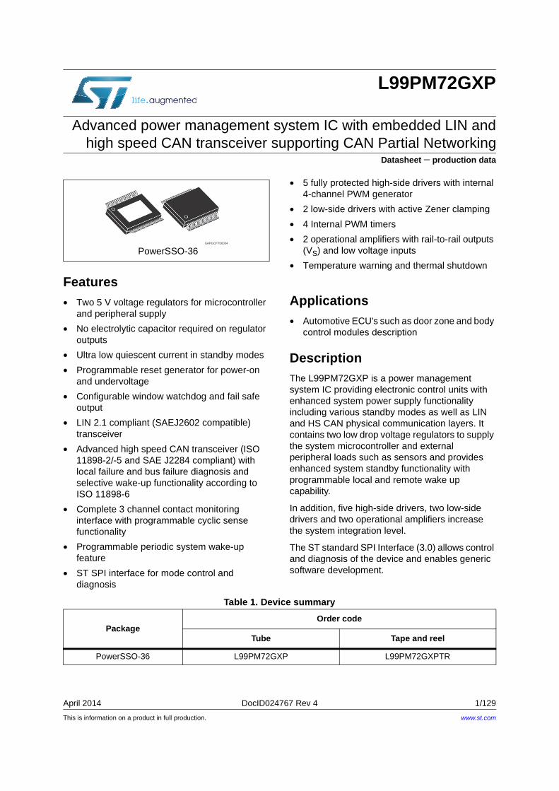
This is information on a product in full production. April 2014 DocID024767 Rev 4 1/129 L99PM72GXP Advanced power management system IC with embedded LIN and high speed CAN transceiver supporting CAN Partial Networking Datasheet − production data Features • Two 5 V voltage regulators for microcontroller and peripheral supply • No electrolytic capacitor required on regulator outputs • Ultra low quiescent current in standby modes • Programmable reset generator for power-on and undervoltage • Configurable window watchdog and fail safe output • LIN 2.1 compliant (SAEJ2602 compatible) transceiver • Advanced high speed CAN transceiver (ISO 11898-2/-5 and SAE J2284 compliant) with local failure and bus failure diagnosis and selective wake-up functionality according to ISO 11898-6 • Complete 3 channel contact monitoring interface with programmable cyclic sense functionality • Programmable periodic system wake-up feature • ST SPI interface for mode control and diagnosis • 5 fully protected high-side drivers with internal 4-channel PWM generator • 2 low-side drivers with active Zener clamping • 4 Internal PWM timers • 2 operational amplifiers with rail-to-rail outputs (V S ) and low voltage inputs • Temperature warning and thermal shutdown Applications • Automotive ECU's such as door zone and body control modules description Description The L99PM72GXP is a power management system IC providing electronic control units with enhanced system power supply functionality including various standby modes as well as LIN and HS CAN physical communication layers. It contains two low drop voltage regulators to supply the system microcontroller and external peripheral loads such as sensors and provides enhanced system standby functionality with programmable local and remote wake up capability. In addition, five high-side drivers, two low-side drivers and two operational amplifiers increase the system integration level. The ST standard SPI Interface (3.0) allows control and diagnosis of the device and enables generic software development. PowerSSO-36 Table 1. Device summary Package Order code Tube Tape and reel PowerSSO-36 L99PM72GXP L99PM72GXPTR www.st.com
Transcript of Advanced power management system IC with embedded LIN and ...
This is information on a product in full production.
April 2014 DocID024767 Rev 4 1/129
L99PM72GXP
Advanced power management system IC with embedded LIN and high speed CAN transceiver supporting CAN Partial Networking
Datasheet − production data
Features• Two 5 V voltage regulators for microcontroller
and peripheral supply
• No electrolytic capacitor required on regulator outputs
• Ultra low quiescent current in standby modes
• Programmable reset generator for power-on and undervoltage
• Configurable window watchdog and fail safe output
• LIN 2.1 compliant (SAEJ2602 compatible) transceiver
• Advanced high speed CAN transceiver (ISO 11898-2/-5 and SAE J2284 compliant) with local failure and bus failure diagnosis and selective wake-up functionality according to ISO 11898-6
• Complete 3 channel contact monitoring interface with programmable cyclic sense functionality
• Programmable periodic system wake-up feature
• ST SPI interface for mode control and diagnosis
• 5 fully protected high-side drivers with internal 4-channel PWM generator
• 2 low-side drivers with active Zener clamping
• 4 Internal PWM timers
• 2 operational amplifiers with rail-to-rail outputs (VS) and low voltage inputs
• Temperature warning and thermal shutdown
Applications• Automotive ECU's such as door zone and body
control modules description
DescriptionThe L99PM72GXP is a power management system IC providing electronic control units with enhanced system power supply functionality including various standby modes as well as LIN and HS CAN physical communication layers. It contains two low drop voltage regulators to supply the system microcontroller and external peripheral loads such as sensors and provides enhanced system standby functionality with programmable local and remote wake up capability.
In addition, five high-side drivers, two low-side drivers and two operational amplifiers increase the system integration level.
The ST standard SPI Interface (3.0) allows control and diagnosis of the device and enables generic software development.
PowerSSO-36
Table 1. Device summary
PackageOrder code
Tube Tape and reel
PowerSSO-36 L99PM72GXP L99PM72GXPTR
www.st.com

Contents L99PM72GXP
2/129 DocID024767 Rev 4
Contents
1 Block diagram and pin description . . . . . . . . . . . . . . . . . . . . . . . . . . . . 10
2 Detailed description . . . . . . . . . . . . . . . . . . . . . . . . . . . . . . . . . . . . . . . . 13
2.1 Voltage regulators . . . . . . . . . . . . . . . . . . . . . . . . . . . . . . . . . . . . . . . . . . 13
2.1.1 Voltage regulator: V1 . . . . . . . . . . . . . . . . . . . . . . . . . . . . . . . . . . . . . . . 13
2.1.2 Voltage regulator: V2 . . . . . . . . . . . . . . . . . . . . . . . . . . . . . . . . . . . . . . . 13
2.1.3 Increased output current capability for voltage regulator V2 . . . . . . . . . 14
2.1.4 Voltage regulator failure . . . . . . . . . . . . . . . . . . . . . . . . . . . . . . . . . . . . . 16
2.1.5 Voltage regulator behavior . . . . . . . . . . . . . . . . . . . . . . . . . . . . . . . . . . . 17
2.2 Operating modes . . . . . . . . . . . . . . . . . . . . . . . . . . . . . . . . . . . . . . . . . . . 17
2.2.1 Active Mode . . . . . . . . . . . . . . . . . . . . . . . . . . . . . . . . . . . . . . . . . . . . . . 17
2.2.2 Flash Mode . . . . . . . . . . . . . . . . . . . . . . . . . . . . . . . . . . . . . . . . . . . . . . 17
2.2.3 SW-Debug Mode . . . . . . . . . . . . . . . . . . . . . . . . . . . . . . . . . . . . . . . . . . 18
2.2.4 V1_standby mode . . . . . . . . . . . . . . . . . . . . . . . . . . . . . . . . . . . . . . . . . . . 18
2.2.5 Interrupt . . . . . . . . . . . . . . . . . . . . . . . . . . . . . . . . . . . . . . . . . . . . . . . . . 19
2.2.6 VBat_standby mode . . . . . . . . . . . . . . . . . . . . . . . . . . . . . . . . . . . . . . . . . 20
2.2.7 Wake up from Standby Modes . . . . . . . . . . . . . . . . . . . . . . . . . . . . . . . . 20
2.2.8 Wake up inputs . . . . . . . . . . . . . . . . . . . . . . . . . . . . . . . . . . . . . . . . . . . 21
2.2.9 Cyclic contact supply . . . . . . . . . . . . . . . . . . . . . . . . . . . . . . . . . . . . . . . 22
2.2.10 Timer interrupt / wake-up of microcontroller by timer . . . . . . . . . . . . . . . 22
2.3 Functional overview (truth table) . . . . . . . . . . . . . . . . . . . . . . . . . . . . . . . 22
2.4 Configurable window watchdog . . . . . . . . . . . . . . . . . . . . . . . . . . . . . . . . 24
2.4.1 Change watchdog timing . . . . . . . . . . . . . . . . . . . . . . . . . . . . . . . . . . . . 26
2.5 Fail Safe Mode . . . . . . . . . . . . . . . . . . . . . . . . . . . . . . . . . . . . . . . . . . . . . 28
2.5.1 Single failures . . . . . . . . . . . . . . . . . . . . . . . . . . . . . . . . . . . . . . . . . . . . 28
2.5.2 Multiple failures – entering forced VBat_standby Mode . . . . . . . . . . . . . . 30
2.6 Reset output (NRESET) . . . . . . . . . . . . . . . . . . . . . . . . . . . . . . . . . . . . . . 31
2.7 Operational amplifiers . . . . . . . . . . . . . . . . . . . . . . . . . . . . . . . . . . . . . . . 31
2.8 LIN Bus Interface . . . . . . . . . . . . . . . . . . . . . . . . . . . . . . . . . . . . . . . . . . . 32
2.8.1 Error handling . . . . . . . . . . . . . . . . . . . . . . . . . . . . . . . . . . . . . . . . . . . . 32
2.8.2 Wake up (from LIN) . . . . . . . . . . . . . . . . . . . . . . . . . . . . . . . . . . . . . . . . 33
2.8.3 LIN Pull-Up . . . . . . . . . . . . . . . . . . . . . . . . . . . . . . . . . . . . . . . . . . . . . . 33
2.9 High speed CAN bus transceiver . . . . . . . . . . . . . . . . . . . . . . . . . . . . . . . 34
DocID024767 Rev 4 3/129
L99PM72GXP Contents
5
2.9.1 CAN transceiver operating modes . . . . . . . . . . . . . . . . . . . . . . . . . . . . . 35
2.9.2 Sequence for enabling selective wakeup . . . . . . . . . . . . . . . . . . . . . . . 37
2.9.3 CAN error handling . . . . . . . . . . . . . . . . . . . . . . . . . . . . . . . . . . . . . . . . 37
2.9.4 Wake up by CAN . . . . . . . . . . . . . . . . . . . . . . . . . . . . . . . . . . . . . . . . . . 38
2.9.5 CAN receive only mode . . . . . . . . . . . . . . . . . . . . . . . . . . . . . . . . . . . . . 40
2.9.6 CAN looping mode . . . . . . . . . . . . . . . . . . . . . . . . . . . . . . . . . . . . . . . . . 40
2.10 Serial Peripheral Interface (ST SPI Standard 3.0) . . . . . . . . . . . . . . . . . . 40
3 Protection and diagnosis . . . . . . . . . . . . . . . . . . . . . . . . . . . . . . . . . . . . 42
3.1 Power supply fail . . . . . . . . . . . . . . . . . . . . . . . . . . . . . . . . . . . . . . . . . . . 42
3.1.1 VS overvoltage . . . . . . . . . . . . . . . . . . . . . . . . . . . . . . . . . . . . . . . . . . . . 42
3.1.2 VS undervoltage . . . . . . . . . . . . . . . . . . . . . . . . . . . . . . . . . . . . . . . . . . . 42
3.2 Temperature warning and thermal shut-down . . . . . . . . . . . . . . . . . . . . . 44
3.3 High side driver outputs . . . . . . . . . . . . . . . . . . . . . . . . . . . . . . . . . . . . . . 45
3.4 Low side driver outputs REL1, REL2 . . . . . . . . . . . . . . . . . . . . . . . . . . . . 46
3.5 SPI diagnosis . . . . . . . . . . . . . . . . . . . . . . . . . . . . . . . . . . . . . . . . . . . . . . 47
4 Typical application . . . . . . . . . . . . . . . . . . . . . . . . . . . . . . . . . . . . . . . . . 48
5 Electrical specifications . . . . . . . . . . . . . . . . . . . . . . . . . . . . . . . . . . . . . 49
5.1 Absolute maximum ratings . . . . . . . . . . . . . . . . . . . . . . . . . . . . . . . . . . . . 49
5.2 ESD protection . . . . . . . . . . . . . . . . . . . . . . . . . . . . . . . . . . . . . . . . . . . . . 50
5.3 Thermal data . . . . . . . . . . . . . . . . . . . . . . . . . . . . . . . . . . . . . . . . . . . . . . 50
5.4 Package and PCB thermal data . . . . . . . . . . . . . . . . . . . . . . . . . . . . . . . . 52
5.4.1 PowerSSO-36 thermal data . . . . . . . . . . . . . . . . . . . . . . . . . . . . . . . . . . 52
5.5 Electrical characteristics . . . . . . . . . . . . . . . . . . . . . . . . . . . . . . . . . . . . . . 55
5.5.1 Supply and supply monitoring . . . . . . . . . . . . . . . . . . . . . . . . . . . . . . . . 55
5.5.2 Oscillator . . . . . . . . . . . . . . . . . . . . . . . . . . . . . . . . . . . . . . . . . . . . . . . . 56
5.5.3 Power-on reset (VS) . . . . . . . . . . . . . . . . . . . . . . . . . . . . . . . . . . . . . . . . 56
5.5.4 Voltage regulator V1 . . . . . . . . . . . . . . . . . . . . . . . . . . . . . . . . . . . . . . . . 56
5.5.5 Voltage regulator V2 . . . . . . . . . . . . . . . . . . . . . . . . . . . . . . . . . . . . . . . . 57
5.5.6 Reset output . . . . . . . . . . . . . . . . . . . . . . . . . . . . . . . . . . . . . . . . . . . . . 58
5.5.7 Watchdog . . . . . . . . . . . . . . . . . . . . . . . . . . . . . . . . . . . . . . . . . . . . . . . . 58
5.5.8 High side outputs . . . . . . . . . . . . . . . . . . . . . . . . . . . . . . . . . . . . . . . . . . 60
5.5.9 Relay drivers . . . . . . . . . . . . . . . . . . . . . . . . . . . . . . . . . . . . . . . . . . . . . 61
5.5.10 Wake up inputs (WU1 ... WU3) . . . . . . . . . . . . . . . . . . . . . . . . . . . . . . . 62

Contents L99PM72GXP
4/129 DocID024767 Rev 4
5.5.11 High speed CAN transceiver . . . . . . . . . . . . . . . . . . . . . . . . . . . . . . . . . 62
5.5.12 LIN transceiver . . . . . . . . . . . . . . . . . . . . . . . . . . . . . . . . . . . . . . . . . . . . 67
5.5.13 Operational amplifier . . . . . . . . . . . . . . . . . . . . . . . . . . . . . . . . . . . . . . . 70
5.5.14 SPI . . . . . . . . . . . . . . . . . . . . . . . . . . . . . . . . . . . . . . . . . . . . . . . . . . . . . 71
5.5.15 Inputs TxDC and TxDL for Flash Mode . . . . . . . . . . . . . . . . . . . . . . . . . 73
6 ST SPI . . . . . . . . . . . . . . . . . . . . . . . . . . . . . . . . . . . . . . . . . . . . . . . . . . . . 77
6.1 SPI communication flow . . . . . . . . . . . . . . . . . . . . . . . . . . . . . . . . . . . . . . 77
6.1.1 General description . . . . . . . . . . . . . . . . . . . . . . . . . . . . . . . . . . . . . . . . 77
6.1.2 Operating code definition . . . . . . . . . . . . . . . . . . . . . . . . . . . . . . . . . . . . 78
6.1.3 Global Status Register . . . . . . . . . . . . . . . . . . . . . . . . . . . . . . . . . . . . . . 78
6.1.4 Configuration register . . . . . . . . . . . . . . . . . . . . . . . . . . . . . . . . . . . . . . 78
6.1.5 Address mapping . . . . . . . . . . . . . . . . . . . . . . . . . . . . . . . . . . . . . . . . . . 80
6.1.6 Write operation . . . . . . . . . . . . . . . . . . . . . . . . . . . . . . . . . . . . . . . . . . . 80
6.1.7 Format of data shifted out at SDO during Write cycle . . . . . . . . . . . . . . 81
6.1.8 Read operation . . . . . . . . . . . . . . . . . . . . . . . . . . . . . . . . . . . . . . . . . . . 82
6.1.9 Format of data shifted out at SDO during Read cycle . . . . . . . . . . . . . . 83
6.1.10 Read and Clear Status Operation . . . . . . . . . . . . . . . . . . . . . . . . . . . . . 84
6.1.11 Read device information . . . . . . . . . . . . . . . . . . . . . . . . . . . . . . . . . . . . 85
6.2 SPI registers . . . . . . . . . . . . . . . . . . . . . . . . . . . . . . . . . . . . . . . . . . . . . . . 87
6.2.1 Overview command byte . . . . . . . . . . . . . . . . . . . . . . . . . . . . . . . . . . . . 87
6.2.2 Overview control register . . . . . . . . . . . . . . . . . . . . . . . . . . . . . . . . . . . . 88
6.2.3 Control Register 1 . . . . . . . . . . . . . . . . . . . . . . . . . . . . . . . . . . . . . . . . . 92
6.2.4 Control Register 2 . . . . . . . . . . . . . . . . . . . . . . . . . . . . . . . . . . . . . . . . . 95
6.2.5 Control Register 3 . . . . . . . . . . . . . . . . . . . . . . . . . . . . . . . . . . . . . . . . . 96
6.2.6 Control Register 4 . . . . . . . . . . . . . . . . . . . . . . . . . . . . . . . . . . . . . . . . . 98
6.2.7 Control Register 5 . . . . . . . . . . . . . . . . . . . . . . . . . . . . . . . . . . . . . . . . 101
6.2.8 Control Register 6 . . . . . . . . . . . . . . . . . . . . . . . . . . . . . . . . . . . . . . . . 103
6.2.9 Control Register 7 . . . . . . . . . . . . . . . . . . . . . . . . . . . . . . . . . . . . . . . . 105
6.2.10 Control Register 8 . . . . . . . . . . . . . . . . . . . . . . . . . . . . . . . . . . . . . . . . 106
6.2.11 Control Register 9 . . . . . . . . . . . . . . . . . . . . . . . . . . . . . . . . . . . . . . . . 107
6.2.12 Control Register 10 . . . . . . . . . . . . . . . . . . . . . . . . . . . . . . . . . . . . . . . 108
6.2.13 Control Register 11 . . . . . . . . . . . . . . . . . . . . . . . . . . . . . . . . . . . . . . . 108
6.2.14 Control Register 12 . . . . . . . . . . . . . . . . . . . . . . . . . . . . . . . . . . . . . . . 109
6.2.15 Control Register 13 . . . . . . . . . . . . . . . . . . . . . . . . . . . . . . . . . . . . . . . 109
6.2.16 Control Register 14 . . . . . . . . . . . . . . . . . . . . . . . . . . . . . . . . . . . . . . . 110
6.2.17 Control Register 15 . . . . . . . . . . . . . . . . . . . . . . . . . . . . . . . . . . . . . . . 111

DocID024767 Rev 4 5/129
L99PM72GXP Contents
5
6.2.18 Control Register 16 . . . . . . . . . . . . . . . . . . . . . . . . . . . . . . . . . . . . . . . 112
6.2.19 Control Register 34 . . . . . . . . . . . . . . . . . . . . . . . . . . . . . . . . . . . . . . . 114
6.2.20 Control Register 35 . . . . . . . . . . . . . . . . . . . . . . . . . . . . . . . . . . . . . . . 115
6.2.21 Overview status register . . . . . . . . . . . . . . . . . . . . . . . . . . . . . . . . . . . 116
6.2.22 Global status register . . . . . . . . . . . . . . . . . . . . . . . . . . . . . . . . . . . . . . 117
6.2.23 Status Register 1 . . . . . . . . . . . . . . . . . . . . . . . . . . . . . . . . . . . . . . . . . 118
6.2.24 Status Register 2 . . . . . . . . . . . . . . . . . . . . . . . . . . . . . . . . . . . . . . . . . 120
6.2.25 Status Register 3 . . . . . . . . . . . . . . . . . . . . . . . . . . . . . . . . . . . . . . . . . 121
6.2.26 Status Register 4 . . . . . . . . . . . . . . . . . . . . . . . . . . . . . . . . . . . . . . . . . 123
6.2.27 Status Register 5 . . . . . . . . . . . . . . . . . . . . . . . . . . . . . . . . . . . . . . . . . 125
7 Package information . . . . . . . . . . . . . . . . . . . . . . . . . . . . . . . . . . . . . . . 126
7.1 ECOPACK® . . . . . . . . . . . . . . . . . . . . . . . . . . . . . . . . . . . . . . . . . . . . . . 126
7.2 PowerSSO-36 mechanical data . . . . . . . . . . . . . . . . . . . . . . . . . . . . . . . 126
8 Revision history . . . . . . . . . . . . . . . . . . . . . . . . . . . . . . . . . . . . . . . . . . 128

List of tables L99PM72GXP
6/129 DocID024767 Rev 4
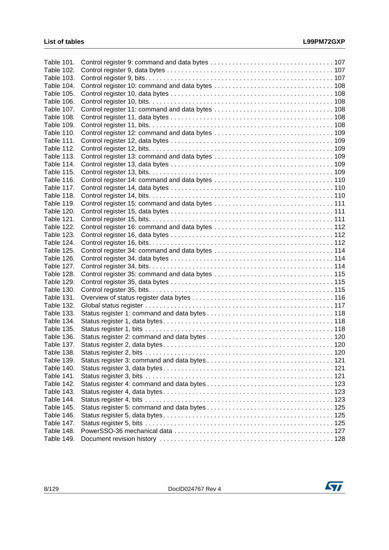
List of tables
Table 1. Device summary . . . . . . . . . . . . . . . . . . . . . . . . . . . . . . . . . . . . . . . . . . . . . . . . . . . . . . . . . . 1Table 2. Pin definitions and functions . . . . . . . . . . . . . . . . . . . . . . . . . . . . . . . . . . . . . . . . . . . . . . . . 11Table 3. CAN wake-up signalization. . . . . . . . . . . . . . . . . . . . . . . . . . . . . . . . . . . . . . . . . . . . . . . . . 19Table 4. Wake up from Standby Modes . . . . . . . . . . . . . . . . . . . . . . . . . . . . . . . . . . . . . . . . . . . . . . 20Table 5. Functional overview (truth table). . . . . . . . . . . . . . . . . . . . . . . . . . . . . . . . . . . . . . . . . . . . . 22Table 6. Fail-Safe conditions and exit modes. . . . . . . . . . . . . . . . . . . . . . . . . . . . . . . . . . . . . . . . . . 29Table 7. Persisting fail safe conditions and exit modes . . . . . . . . . . . . . . . . . . . . . . . . . . . . . . . . . . 31Table 8. PWM configuration for high-side outputs . . . . . . . . . . . . . . . . . . . . . . . . . . . . . . . . . . . . . . 45Table 9. Absolute maximum ratings . . . . . . . . . . . . . . . . . . . . . . . . . . . . . . . . . . . . . . . . . . . . . . . . . 49Table 10. ESD protection . . . . . . . . . . . . . . . . . . . . . . . . . . . . . . . . . . . . . . . . . . . . . . . . . . . . . . . . . . 50Table 11. Operating junction temperature . . . . . . . . . . . . . . . . . . . . . . . . . . . . . . . . . . . . . . . . . . . . . 50Table 12. Temperature warning and thermal shutdown . . . . . . . . . . . . . . . . . . . . . . . . . . . . . . . . . . . 50Table 13. Thermal parameter . . . . . . . . . . . . . . . . . . . . . . . . . . . . . . . . . . . . . . . . . . . . . . . . . . . . . . . 54Table 14. Supply and supply monitoring. . . . . . . . . . . . . . . . . . . . . . . . . . . . . . . . . . . . . . . . . . . . . . . 55Table 15. Oscillator . . . . . . . . . . . . . . . . . . . . . . . . . . . . . . . . . . . . . . . . . . . . . . . . . . . . . . . . . . . . . . . 56Table 16. Power-on reset (VS) . . . . . . . . . . . . . . . . . . . . . . . . . . . . . . . . . . . . . . . . . . . . . . . . . . . . . . 56Table 17. Voltage regulator V1 . . . . . . . . . . . . . . . . . . . . . . . . . . . . . . . . . . . . . . . . . . . . . . . . . . . . . . 56Table 18. Voltage regulator V2 . . . . . . . . . . . . . . . . . . . . . . . . . . . . . . . . . . . . . . . . . . . . . . . . . . . . . . 57Table 19. Reset output . . . . . . . . . . . . . . . . . . . . . . . . . . . . . . . . . . . . . . . . . . . . . . . . . . . . . . . . . . . . 58Table 20. Watchdog . . . . . . . . . . . . . . . . . . . . . . . . . . . . . . . . . . . . . . . . . . . . . . . . . . . . . . . . . . . . . . 58Table 21. Output (OUT_HS) . . . . . . . . . . . . . . . . . . . . . . . . . . . . . . . . . . . . . . . . . . . . . . . . . . . . . . . . 60Table 22. Outputs (OUT1...4) . . . . . . . . . . . . . . . . . . . . . . . . . . . . . . . . . . . . . . . . . . . . . . . . . . . . . . . 61Table 23. Relay drivers. . . . . . . . . . . . . . . . . . . . . . . . . . . . . . . . . . . . . . . . . . . . . . . . . . . . . . . . . . . . 61Table 24. Wake-up inputs. . . . . . . . . . . . . . . . . . . . . . . . . . . . . . . . . . . . . . . . . . . . . . . . . . . . . . . . . . 62Table 25. CAN communication operating range. . . . . . . . . . . . . . . . . . . . . . . . . . . . . . . . . . . . . . . . . 62Table 26. CAN transmit data input: pin TxDC. . . . . . . . . . . . . . . . . . . . . . . . . . . . . . . . . . . . . . . . . . . 62Table 27. CAN receive data output: pin RxDC . . . . . . . . . . . . . . . . . . . . . . . . . . . . . . . . . . . . . . . . . . 63Table 28. CAN transmitter and receiver: pins CANH and CANL . . . . . . . . . . . . . . . . . . . . . . . . . . . . 63Table 29. CAN transceiver timing . . . . . . . . . . . . . . . . . . . . . . . . . . . . . . . . . . . . . . . . . . . . . . . . . . . . 65Table 30. LIN transmit data input: pin TxD . . . . . . . . . . . . . . . . . . . . . . . . . . . . . . . . . . . . . . . . . . . . . 67Table 31. LIN receive data output: pin RxD . . . . . . . . . . . . . . . . . . . . . . . . . . . . . . . . . . . . . . . . . . . . 67Table 32. LIN transmitter and receiver: pin LIN . . . . . . . . . . . . . . . . . . . . . . . . . . . . . . . . . . . . . . . . . 67Table 33. LIN transceiver timing . . . . . . . . . . . . . . . . . . . . . . . . . . . . . . . . . . . . . . . . . . . . . . . . . . . . . 68Table 34. LIN pull-up: pin LINPU . . . . . . . . . . . . . . . . . . . . . . . . . . . . . . . . . . . . . . . . . . . . . . . . . . . . 69Table 35. Operational amplifier. . . . . . . . . . . . . . . . . . . . . . . . . . . . . . . . . . . . . . . . . . . . . . . . . . . . . . 70Table 36. Input: CSN . . . . . . . . . . . . . . . . . . . . . . . . . . . . . . . . . . . . . . . . . . . . . . . . . . . . . . . . . . . . . 71Table 37. Inputs: CLK, DI . . . . . . . . . . . . . . . . . . . . . . . . . . . . . . . . . . . . . . . . . . . . . . . . . . . . . . . . . . 71Table 38. DI timing . . . . . . . . . . . . . . . . . . . . . . . . . . . . . . . . . . . . . . . . . . . . . . . . . . . . . . . . . . . . . . . 71Table 39. Output: DO . . . . . . . . . . . . . . . . . . . . . . . . . . . . . . . . . . . . . . . . . . . . . . . . . . . . . . . . . . . . . 72Table 40. DO timing . . . . . . . . . . . . . . . . . . . . . . . . . . . . . . . . . . . . . . . . . . . . . . . . . . . . . . . . . . . . . . 72Table 41. CSN timing . . . . . . . . . . . . . . . . . . . . . . . . . . . . . . . . . . . . . . . . . . . . . . . . . . . . . . . . . . . . . 72Table 42. RXDL/NINT, RXDC/NINT timing. . . . . . . . . . . . . . . . . . . . . . . . . . . . . . . . . . . . . . . . . . . . . 73Table 43. Inputs: TxDC and TxDL for Flash Mode . . . . . . . . . . . . . . . . . . . . . . . . . . . . . . . . . . . . . . . 73Table 44. Command Byte . . . . . . . . . . . . . . . . . . . . . . . . . . . . . . . . . . . . . . . . . . . . . . . . . . . . . . . . . . 77Table 45. Operating code definition . . . . . . . . . . . . . . . . . . . . . . . . . . . . . . . . . . . . . . . . . . . . . . . . . . 78Table 46. Global status register . . . . . . . . . . . . . . . . . . . . . . . . . . . . . . . . . . . . . . . . . . . . . . . . . . . . . 78Table 47. Configuration register . . . . . . . . . . . . . . . . . . . . . . . . . . . . . . . . . . . . . . . . . . . . . . . . . . . . . 78Table 48. Address mapping . . . . . . . . . . . . . . . . . . . . . . . . . . . . . . . . . . . . . . . . . . . . . . . . . . . . . . . . 80

DocID024767 Rev 4 7/129
L99PM72GXP List of tables
8
Table 49. Write command format: command byte . . . . . . . . . . . . . . . . . . . . . . . . . . . . . . . . . . . . . . . 80Table 50. Write command format: data byte 1 . . . . . . . . . . . . . . . . . . . . . . . . . . . . . . . . . . . . . . . . . . 81Table 51. Write command format: data byte 2 . . . . . . . . . . . . . . . . . . . . . . . . . . . . . . . . . . . . . . . . . . 81Table 52. Format of data shifted out at SDO during write cycle: global status register . . . . . . . . . . . 81Table 53. Format of data shifted out at SDO during write cycle: data byte 1 . . . . . . . . . . . . . . . . . . . 81Table 54. Format of data shifted out at SDO during write cycle: data byte 2 . . . . . . . . . . . . . . . . . . . 81Table 55. Read command format: command byte . . . . . . . . . . . . . . . . . . . . . . . . . . . . . . . . . . . . . . . 82Table 56. Read command format: data byte 1 . . . . . . . . . . . . . . . . . . . . . . . . . . . . . . . . . . . . . . . . . . 82Table 57. Read command format: data byte 2 . . . . . . . . . . . . . . . . . . . . . . . . . . . . . . . . . . . . . . . . . . 82Table 58. Format of data shifted out at SDO during read cycle: global status register. . . . . . . . . . . . 83Table 59. Format of data shifted out at SDO during read cycle: data byte 1 . . . . . . . . . . . . . . . . . . . 83Table 60. Format of data shifted out at SDO during read cycle: data byte 2 . . . . . . . . . . . . . . . . . . . 83Table 61. Read and clear status command format: command byte . . . . . . . . . . . . . . . . . . . . . . . . . . 84Table 62. Read and clear status command format: data byte 1 . . . . . . . . . . . . . . . . . . . . . . . . . . . . . 84Table 63. Read and clear status command format: data byte 2 . . . . . . . . . . . . . . . . . . . . . . . . . . . . . 84Table 64. Format of data shifted out at SDO during read and clear status: global status register . . . 84Table 65. Format of data shifted out at SDO during read and clear status: data byte 1. . . . . . . . . . . 84Table 66. Format of data shifted out at SDO during read and clear status: data byte 2. . . . . . . . . . . 84Table 67. Read device information . . . . . . . . . . . . . . . . . . . . . . . . . . . . . . . . . . . . . . . . . . . . . . . . . . . 85Table 68. ID-header . . . . . . . . . . . . . . . . . . . . . . . . . . . . . . . . . . . . . . . . . . . . . . . . . . . . . . . . . . . . . . 86Table 69. Family identifier. . . . . . . . . . . . . . . . . . . . . . . . . . . . . . . . . . . . . . . . . . . . . . . . . . . . . . . . . . 86Table 70. Silicon version identifier . . . . . . . . . . . . . . . . . . . . . . . . . . . . . . . . . . . . . . . . . . . . . . . . . . . 86Table 71. SPI-frame-ID. . . . . . . . . . . . . . . . . . . . . . . . . . . . . . . . . . . . . . . . . . . . . . . . . . . . . . . . . . . . 86Table 72. SPI register: command byte . . . . . . . . . . . . . . . . . . . . . . . . . . . . . . . . . . . . . . . . . . . . . . . . 87Table 73. SPI register: mode selection . . . . . . . . . . . . . . . . . . . . . . . . . . . . . . . . . . . . . . . . . . . . . . . . 87Table 74. SPI register: CTRL register selection . . . . . . . . . . . . . . . . . . . . . . . . . . . . . . . . . . . . . . . . . 87Table 75. SPI register: STAT register selection . . . . . . . . . . . . . . . . . . . . . . . . . . . . . . . . . . . . . . . . . 88Table 76. Overview of control register data bytes . . . . . . . . . . . . . . . . . . . . . . . . . . . . . . . . . . . . . . . 88Table 77. Control register 1: command and data bytes . . . . . . . . . . . . . . . . . . . . . . . . . . . . . . . . . . . 92Table 78. Control register 1, data bytes . . . . . . . . . . . . . . . . . . . . . . . . . . . . . . . . . . . . . . . . . . . . . . . 92Table 79. Control register 1, bits. . . . . . . . . . . . . . . . . . . . . . . . . . . . . . . . . . . . . . . . . . . . . . . . . . . . . 92Table 80. Control register 2: command and data bytes . . . . . . . . . . . . . . . . . . . . . . . . . . . . . . . . . . . 95Table 81. Control register 2, data bytes . . . . . . . . . . . . . . . . . . . . . . . . . . . . . . . . . . . . . . . . . . . . . . . 95Table 82. Control register 2, bits. . . . . . . . . . . . . . . . . . . . . . . . . . . . . . . . . . . . . . . . . . . . . . . . . . . . . 95Table 83. Control register 3: command and data bytes . . . . . . . . . . . . . . . . . . . . . . . . . . . . . . . . . . . 96Table 84. Control register 3, data bytes . . . . . . . . . . . . . . . . . . . . . . . . . . . . . . . . . . . . . . . . . . . . . . . 96Table 85. Control register 3, bits. . . . . . . . . . . . . . . . . . . . . . . . . . . . . . . . . . . . . . . . . . . . . . . . . . . . . 97Table 86. Control register 4: command and data bytes . . . . . . . . . . . . . . . . . . . . . . . . . . . . . . . . . . . 98Table 87. Control register 4, data bytes . . . . . . . . . . . . . . . . . . . . . . . . . . . . . . . . . . . . . . . . . . . . . . . 99Table 88. Control register 4, bits. . . . . . . . . . . . . . . . . . . . . . . . . . . . . . . . . . . . . . . . . . . . . . . . . . . . . 99Table 89. Control register 5: command and data bytes . . . . . . . . . . . . . . . . . . . . . . . . . . . . . . . . . . 101Table 90. Control register 5, data bytes . . . . . . . . . . . . . . . . . . . . . . . . . . . . . . . . . . . . . . . . . . . . . . 101Table 91. Control register 5, bits. . . . . . . . . . . . . . . . . . . . . . . . . . . . . . . . . . . . . . . . . . . . . . . . . . . . 102Table 92. Control register 6: command and data bytes . . . . . . . . . . . . . . . . . . . . . . . . . . . . . . . . . . 103Table 93. Control register 6, data bytes . . . . . . . . . . . . . . . . . . . . . . . . . . . . . . . . . . . . . . . . . . . . . . 103Table 94. Control register 6, bits. . . . . . . . . . . . . . . . . . . . . . . . . . . . . . . . . . . . . . . . . . . . . . . . . . . . 103Table 95. Control register 7: command and data bytes . . . . . . . . . . . . . . . . . . . . . . . . . . . . . . . . . . 105Table 96. Control register 7, data bytes . . . . . . . . . . . . . . . . . . . . . . . . . . . . . . . . . . . . . . . . . . . . . . 105Table 97. Control register 7, bits. . . . . . . . . . . . . . . . . . . . . . . . . . . . . . . . . . . . . . . . . . . . . . . . . . . . 105Table 98. Control register 8: command and data bytes . . . . . . . . . . . . . . . . . . . . . . . . . . . . . . . . . . 106Table 99. Control register 8, data bytes . . . . . . . . . . . . . . . . . . . . . . . . . . . . . . . . . . . . . . . . . . . . . . 106Table 100. Control register 8, bits. . . . . . . . . . . . . . . . . . . . . . . . . . . . . . . . . . . . . . . . . . . . . . . . . . . . 106
List of tables L99PM72GXP
8/129 DocID024767 Rev 4
Table 101. Control register 9: command and data bytes . . . . . . . . . . . . . . . . . . . . . . . . . . . . . . . . . . 107Table 102. Control register 9, data bytes . . . . . . . . . . . . . . . . . . . . . . . . . . . . . . . . . . . . . . . . . . . . . . 107Table 103. Control register 9, bits. . . . . . . . . . . . . . . . . . . . . . . . . . . . . . . . . . . . . . . . . . . . . . . . . . . . 107Table 104. Control register 10: command and data bytes . . . . . . . . . . . . . . . . . . . . . . . . . . . . . . . . . 108Table 105. Control register 10, data bytes . . . . . . . . . . . . . . . . . . . . . . . . . . . . . . . . . . . . . . . . . . . . . 108Table 106. Control register 10, bits. . . . . . . . . . . . . . . . . . . . . . . . . . . . . . . . . . . . . . . . . . . . . . . . . . . 108Table 107. Control register 11: command and data bytes . . . . . . . . . . . . . . . . . . . . . . . . . . . . . . . . . 108Table 108. Control register 11, data bytes . . . . . . . . . . . . . . . . . . . . . . . . . . . . . . . . . . . . . . . . . . . . . 108Table 109. Control register 11, bits. . . . . . . . . . . . . . . . . . . . . . . . . . . . . . . . . . . . . . . . . . . . . . . . . . . 108Table 110. Control register 12: command and data bytes . . . . . . . . . . . . . . . . . . . . . . . . . . . . . . . . . 109Table 111. Control register 12, data bytes . . . . . . . . . . . . . . . . . . . . . . . . . . . . . . . . . . . . . . . . . . . . . 109Table 112. Control register 12, bits. . . . . . . . . . . . . . . . . . . . . . . . . . . . . . . . . . . . . . . . . . . . . . . . . . . 109Table 113. Control register 13: command and data bytes . . . . . . . . . . . . . . . . . . . . . . . . . . . . . . . . . 109Table 114. Control register 13, data bytes . . . . . . . . . . . . . . . . . . . . . . . . . . . . . . . . . . . . . . . . . . . . . 109Table 115. Control register 13, bits. . . . . . . . . . . . . . . . . . . . . . . . . . . . . . . . . . . . . . . . . . . . . . . . . . . 109Table 116. Control register 14: command and data bytes . . . . . . . . . . . . . . . . . . . . . . . . . . . . . . . . . 110Table 117. Control register 14, data bytes . . . . . . . . . . . . . . . . . . . . . . . . . . . . . . . . . . . . . . . . . . . . . 110Table 118. Control register 14, bits. . . . . . . . . . . . . . . . . . . . . . . . . . . . . . . . . . . . . . . . . . . . . . . . . . . 110Table 119. Control register 15: command and data bytes . . . . . . . . . . . . . . . . . . . . . . . . . . . . . . . . . 111Table 120. Control register 15, data bytes . . . . . . . . . . . . . . . . . . . . . . . . . . . . . . . . . . . . . . . . . . . . . 111Table 121. Control register 15, bits. . . . . . . . . . . . . . . . . . . . . . . . . . . . . . . . . . . . . . . . . . . . . . . . . . . 111Table 122. Control register 16: command and data bytes . . . . . . . . . . . . . . . . . . . . . . . . . . . . . . . . . 112Table 123. Control register 16, data bytes . . . . . . . . . . . . . . . . . . . . . . . . . . . . . . . . . . . . . . . . . . . . . 112Table 124. Control register 16, bits. . . . . . . . . . . . . . . . . . . . . . . . . . . . . . . . . . . . . . . . . . . . . . . . . . . 112Table 125. Control register 34: command and data bytes . . . . . . . . . . . . . . . . . . . . . . . . . . . . . . . . . 114Table 126. Control register 34, data bytes . . . . . . . . . . . . . . . . . . . . . . . . . . . . . . . . . . . . . . . . . . . . . 114Table 127. Control register 34, bits. . . . . . . . . . . . . . . . . . . . . . . . . . . . . . . . . . . . . . . . . . . . . . . . . . . 114Table 128. Control register 35: command and data bytes . . . . . . . . . . . . . . . . . . . . . . . . . . . . . . . . . 115Table 129. Control register 35, data bytes . . . . . . . . . . . . . . . . . . . . . . . . . . . . . . . . . . . . . . . . . . . . . 115Table 130. Control register 35, bits. . . . . . . . . . . . . . . . . . . . . . . . . . . . . . . . . . . . . . . . . . . . . . . . . . . 115Table 131. Overview of status register data bytes . . . . . . . . . . . . . . . . . . . . . . . . . . . . . . . . . . . . . . . 116Table 132. Global status register . . . . . . . . . . . . . . . . . . . . . . . . . . . . . . . . . . . . . . . . . . . . . . . . . . . . 117Table 133. Status register 1: command and data bytes . . . . . . . . . . . . . . . . . . . . . . . . . . . . . . . . . . . 118Table 134. Status register 1, data bytes . . . . . . . . . . . . . . . . . . . . . . . . . . . . . . . . . . . . . . . . . . . . . . . 118Table 135. Status register 1, bits . . . . . . . . . . . . . . . . . . . . . . . . . . . . . . . . . . . . . . . . . . . . . . . . . . . . 118Table 136. Status register 2: command and data bytes . . . . . . . . . . . . . . . . . . . . . . . . . . . . . . . . . . . 120Table 137. Status register 2, data bytes . . . . . . . . . . . . . . . . . . . . . . . . . . . . . . . . . . . . . . . . . . . . . . . 120Table 138. Status register 2, bits . . . . . . . . . . . . . . . . . . . . . . . . . . . . . . . . . . . . . . . . . . . . . . . . . . . . 120Table 139. Status register 3: command and data bytes . . . . . . . . . . . . . . . . . . . . . . . . . . . . . . . . . . . 121Table 140. Status register 3, data bytes . . . . . . . . . . . . . . . . . . . . . . . . . . . . . . . . . . . . . . . . . . . . . . . 121Table 141. Status register 3, bits . . . . . . . . . . . . . . . . . . . . . . . . . . . . . . . . . . . . . . . . . . . . . . . . . . . . 121Table 142. Status register 4: command and data bytes . . . . . . . . . . . . . . . . . . . . . . . . . . . . . . . . . . . 123Table 143. Status register 4, data bytes . . . . . . . . . . . . . . . . . . . . . . . . . . . . . . . . . . . . . . . . . . . . . . . 123Table 144. Status register 4, bits . . . . . . . . . . . . . . . . . . . . . . . . . . . . . . . . . . . . . . . . . . . . . . . . . . . . 123Table 145. Status register 5: command and data bytes . . . . . . . . . . . . . . . . . . . . . . . . . . . . . . . . . . . 125Table 146. Status register 5, data bytes . . . . . . . . . . . . . . . . . . . . . . . . . . . . . . . . . . . . . . . . . . . . . . . 125Table 147. Status register 5, bits . . . . . . . . . . . . . . . . . . . . . . . . . . . . . . . . . . . . . . . . . . . . . . . . . . . . 125Table 148. PowerSSO-36 mechanical data . . . . . . . . . . . . . . . . . . . . . . . . . . . . . . . . . . . . . . . . . . . . 127Table 149. Document revision history . . . . . . . . . . . . . . . . . . . . . . . . . . . . . . . . . . . . . . . . . . . . . . . . 128

DocID024767 Rev 4 9/129
L99PM72GXP List of figures
9
List of figures
Figure 1. Block diagram . . . . . . . . . . . . . . . . . . . . . . . . . . . . . . . . . . . . . . . . . . . . . . . . . . . . . . . . . . . 10Figure 2. Pin connection (top view) . . . . . . . . . . . . . . . . . . . . . . . . . . . . . . . . . . . . . . . . . . . . . . . . . . 12Figure 3. Voltage source with external PNP . . . . . . . . . . . . . . . . . . . . . . . . . . . . . . . . . . . . . . . . . . . 14Figure 4. Voltage source with external PNP and current limitation . . . . . . . . . . . . . . . . . . . . . . . . . . 14Figure 5. Voltage source with external NPN . . . . . . . . . . . . . . . . . . . . . . . . . . . . . . . . . . . . . . . . . . . 15Figure 6. Voltage source with external NPN and current limitation . . . . . . . . . . . . . . . . . . . . . . . . . . 15Figure 7. Voltage regulator behaviour and diagnosis during supply voltage ramp-up / ramp-down
conditions . . . . . . . . . . . . . . . . . . . . . . . . . . . . . . . . . . . . . . . . . . . . . . . . . . . . . . . . . . . . . . 17Figure 8. Sequence to enter and exit SW Debug Mode . . . . . . . . . . . . . . . . . . . . . . . . . . . . . . . . . . 18Figure 9. Main operating modes . . . . . . . . . . . . . . . . . . . . . . . . . . . . . . . . . . . . . . . . . . . . . . . . . . . . 24Figure 10. Watchdog in normal operating mode (no errors) . . . . . . . . . . . . . . . . . . . . . . . . . . . . . . . . 25Figure 11. Watchdog with error conditions . . . . . . . . . . . . . . . . . . . . . . . . . . . . . . . . . . . . . . . . . . . . . 26Figure 12. Watchdog in FLASH Mode . . . . . . . . . . . . . . . . . . . . . . . . . . . . . . . . . . . . . . . . . . . . . . . . . 26Figure 13. Change watchdog timing within long open window . . . . . . . . . . . . . . . . . . . . . . . . . . . . . . 27Figure 14. Change watchdog timing within window mode . . . . . . . . . . . . . . . . . . . . . . . . . . . . . . . . . . 27Figure 15. General procedure to change watchdog timing out of Fail safe mode . . . . . . . . . . . . . . . . 28Figure 16. Change watchdog timing out of Fail safe mode (Watchdog failure) . . . . . . . . . . . . . . . . . . 28Figure 17. Example: exit Fail-Safe mode from Watchdog failure. . . . . . . . . . . . . . . . . . . . . . . . . . . . . 30Figure 18. Master node configuration using LIN_PU (optional) . . . . . . . . . . . . . . . . . . . . . . . . . . . . . . 33Figure 19. Transceiver state diagram if selective wake-up is disabled (CR16 SW_EN = 0) . . . . . . . . 35Figure 20. CAN transceiver state diagram if selective wake-up is enabled (CR16 SW_EN = 1). . . . . 36Figure 21. CAN wake up capabilities . . . . . . . . . . . . . . . . . . . . . . . . . . . . . . . . . . . . . . . . . . . . . . . . . . 39Figure 22. Overvoltage and undervoltage protection and diagnosis . . . . . . . . . . . . . . . . . . . . . . . . . . 43Figure 23. Thermal shutdown protection and diagnosis . . . . . . . . . . . . . . . . . . . . . . . . . . . . . . . . . . . 44Figure 24. Phase shifted PWM . . . . . . . . . . . . . . . . . . . . . . . . . . . . . . . . . . . . . . . . . . . . . . . . . . . . . . 46Figure 25. Typical application diagram . . . . . . . . . . . . . . . . . . . . . . . . . . . . . . . . . . . . . . . . . . . . . . . . 48Figure 26. Thermal data of PowerSSO-36. . . . . . . . . . . . . . . . . . . . . . . . . . . . . . . . . . . . . . . . . . . . . . 51Figure 27. PowerSSO-36 PC board. . . . . . . . . . . . . . . . . . . . . . . . . . . . . . . . . . . . . . . . . . . . . . . . . . . 52Figure 28. PowerSSO-36 thermal resistance junction to ambient vs PCB copper area (V1 ON) . . . . 53Figure 29. PowerSSO-36 thermal impedance junction to ambient vs PCB copper area (single pulse
with V1 ON). . . . . . . . . . . . . . . . . . . . . . . . . . . . . . . . . . . . . . . . . . . . . . . . . . . . . . . . . . . . . 53Figure 30. PowerSSO-36 thermal fitting model (V1 ON) . . . . . . . . . . . . . . . . . . . . . . . . . . . . . . . . . . . 54Figure 31. Watchdog timing (long, early, late and safe window) . . . . . . . . . . . . . . . . . . . . . . . . . . . . . 59Figure 32. Watchdog early, late and safe windows . . . . . . . . . . . . . . . . . . . . . . . . . . . . . . . . . . . . . . . 60Figure 33. LIN transmit, receive timing . . . . . . . . . . . . . . . . . . . . . . . . . . . . . . . . . . . . . . . . . . . . . . . . 70Figure 34. SPI - transfer timing diagram . . . . . . . . . . . . . . . . . . . . . . . . . . . . . . . . . . . . . . . . . . . . . . . 73Figure 35. SPI input timing. . . . . . . . . . . . . . . . . . . . . . . . . . . . . . . . . . . . . . . . . . . . . . . . . . . . . . . . . . 74Figure 36. SPI output timing (part 1) . . . . . . . . . . . . . . . . . . . . . . . . . . . . . . . . . . . . . . . . . . . . . . . . . . 75Figure 37. SPI CSN - output timing . . . . . . . . . . . . . . . . . . . . . . . . . . . . . . . . . . . . . . . . . . . . . . . . . . . 76Figure 38. SPI - CSN low to high transition and global status bit access . . . . . . . . . . . . . . . . . . . . . . 76Figure 39. Read configuration register. . . . . . . . . . . . . . . . . . . . . . . . . . . . . . . . . . . . . . . . . . . . . . . . . 79Figure 40. Write configuration register . . . . . . . . . . . . . . . . . . . . . . . . . . . . . . . . . . . . . . . . . . . . . . . . . 79Figure 41. Format of data shifted out at SDO during write cycle . . . . . . . . . . . . . . . . . . . . . . . . . . . . . 82Figure 42. Format of data shifted out at SDO during read cycle . . . . . . . . . . . . . . . . . . . . . . . . . . . . . 83Figure 43. Format of data shifted out at SDO during read and clear status operation . . . . . . . . . . . . 85Figure 44. PowerSSO-36 package dimensions . . . . . . . . . . . . . . . . . . . . . . . . . . . . . . . . . . . . . . . . . 126
Block diagram and pin description L99PM72GXP
10/129 DocID024767 Rev 4
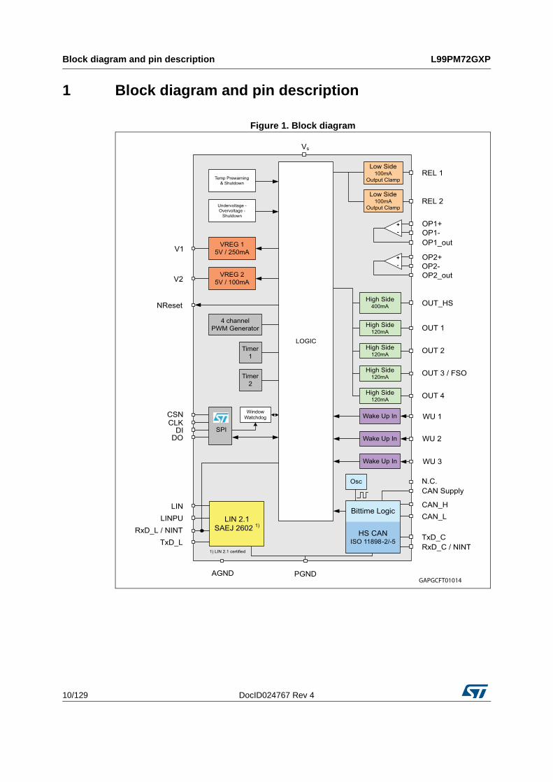
1 Block diagram and pin description
Figure 1. Block diagram

DocID024767 Rev 4 11/129
L99PM72GXP Block diagram and pin description
128
Table 2. Pin definitions and functions
Pin Symbol Function
1 AGND Analog ground
2 RxDC/NINTRxDC -> CAN receive data output
NINT -> indicates remote CAN wake-up events in Active Mode (transceiver in TRX_STBY; CAN_ACT = 0)
3 TxDC CAN transmit data Input
4 CANH CAN high level voltage I/O
5 CANL CAN low level voltage I/O
6 N.C. TBC
7 CANSUP CAN supply input; to allow external CAN supply from V1 or V2 regulator.
8 NRESETNRESET output to microcontroller; Internal pull-up of typ. 100 KΩ (reset state = LOW)
9 V1 Voltage regulator 1 output: 5 V supply e.g. micro controller, CAN transceiver
10 V2Voltage regulator 2 output: 5 V supply for external loads (IR receiver, potentiometer, sensors) or CAN transceiver. V2 is protected against reverse supply.
11 TxDL LIN transmit data input
12 RxDL/NINTRxDL -> LIN receive data outputNINT -> indicates local/remote wake-up events except CAN wake-up in Active Mode provides a programmable timer interrupt signal
13 OP2+ Non inverting input of operational amplifier 2
14 OP2- Inverting input of operational amplifier 2
15 OP2_OUT Output of operational amplifier 2
16 DI SPI: serial data input
17 DO SPI: serial data output
18 CLK SPI: serial clock input
19 CSN SPI: chip select not input
20…22 WU1…3Wake-up Inputs 1…3: Input pins for static or cyclic monitoring of external contacts
23 OP1_OUT Output of operational amplifier 1
24 OP1- Inverting input of operational amplifier 1
25 OP1+ Non inverting input of operational amplifier 1
26 OUT4 High side driver output (7Ω, typ)
27 OUT3/FSO
Configurable as:
– High-side driver output (7Ω, typ) – Fail safe output pin (default)
28 OUT2 High side driver output (7Ω, typ)
29 OUT1 High side driver output (7Ω, typ)
30 OUT_HS High side driver (1 Ω, typ)

Block diagram and pin description L99PM72GXP
12/129 DocID024767 Rev 4
Figure 2. Pin connection (top view)
31 VS Power supply voltage
32 LINPU High side driver output to switch off LIN master pull up resistor
33 LIN LIN bus line
34 REL1 Low side driver output (2 Ω typ)
35 REL2 Low side driver output (2 Ω typ)
36 PGNDPower ground (REL1/2, LIN and CAN GND), to be connected to AGND externally
Table 2. Pin definitions and functions (continued)
Pin Symbol Function
CANH
DO
CLK
V2
OUT_HS
AGND 1
RxDC / NINT 2
TxDC 3
4
5
NRESET
6
V1
7
8
TxDL
9
RxDL / NINT
10
OP2P
11
OP2M
12
OPOUT2
13
DI
14
N.C.
15
CANSUP
16
17
18
PGND36
Vs
35
REL134
REL2
33
32
OUT3/FSO
31
OUT1
30
29
OUT4
28
OP1P
27
OP1M
26
OPOUT1
25
WU3
24
WU2
23
WU1
22
CSN
21
LINPU
20
LIN
19
OUT2PowerSSO-36
CANL
TAB = AGND
DocID024767 Rev 4 13/129
L99PM72GXP Detailed description
128
2 Detailed description
2.1 Voltage regulatorsThe L99PM72GXP contains two independent and fully protected low drop voltage regulators, which are designed for very fast transient response and do not require electrolytic output capacitors for stability.
The output voltage is stable with ceramic load capacitors ≥ 220 nF.
2.1.1 Voltage regulator: V1
The V1 voltage regulator provides 5 V supply voltage and up to 250 mA continuous load current and is mainly intended for supply of the system microcontroller. The V1 regulator is embedded in the power management and Fail_safe functionality of the device and operates according to the selected operating mode.
It can be used to supply the internal HS CAN Transceiver via the CANSUP pin externally. In case of a short circuit condition on the CAN bus, the output current of the transmitter is limited to 100 mA and the transceiver is turned off in order to ensure continued supply of the microcontroller.
In addition the regulator V1 drives the L99PM72GXP internal 5 V loads. The voltage regulator is protected against overload and overtemperature. An external reverse current protection has to be provided by the application circuitry to prevent the input capacitor from being discharged by negative transients or low input voltage. Current limitation of the regulator ensures fast charge of external bypass capacitors. The output voltage is stable for ceramic load capacitors ≥ 220 nF.
If the device temperature exceeds the TSD1 threshold, all outputs (OUTx, RELx, V2, LIN) are deactivated except V1. Hence the micro controller has the possibility for interaction or error logging. In case of exceeding TSD2 threshold (TSD2 > TSD1), also V1 is deactivated (see Figure 23: Thermal shutdown protection and diagnosis). A timer is started and the voltage regulator is deactivated for tTSD = 1 sec. During this time, all other wakeup sources (CAN, LIN, WU1...3 and wake up of µC by timer) are disabled. After 1 sec, the voltage regulator tries to restart automatically. If the restart fails 7 times, within one minute, without clearing and thermal shutdown condition still exists, the L99PM72GXP enters the Forced VBat_standby Mode.
In case of short to GND at "V1" after initial turn on (V1 < 2 V for t > tV1 short) the L99PM72GXP enters the Forced VBat_standby Mode. Reactivation (wake-up) of the device can be achieved with signals from CAN, LIN, WU1..3 or periodic wake by timer.
2.1.2 Voltage regulator: V2
The voltage regulator V2 can supply additional 5 V loads (e.g. logic components or the integrated HS CAN transceiver or external loads such as sensors or potentiometers. The maximum continuous load current is 100 mA. The regulator is protected against:
• Overload
• Overtemperature
• Short circuit (short to ground and battery supply voltage)
• Reverse biasing
Detailed description L99PM72GXP
14/129 DocID024767 Rev 4
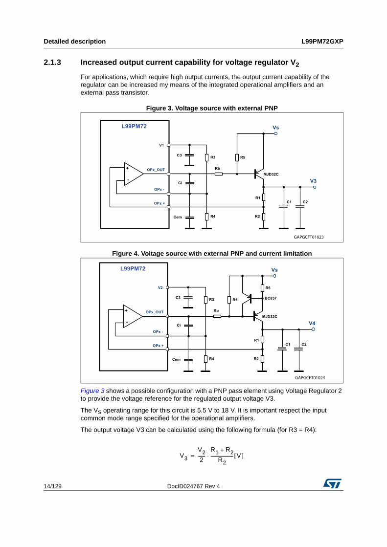
2.1.3 Increased output current capability for voltage regulator V2
For applications, which require high output currents, the output current capability of the regulator can be increased my means of the integrated operational amplifiers and an external pass transistor.
Figure 3. Voltage source with external PNP
Figure 4. Voltage source with external PNP and current limitation
Figure 3 shows a possible configuration with a PNP pass element using Voltage Regulator 2 to provide the voltage reference for the regulated output voltage V3.
The VS operating range for this circuit is 5.5 V to 18 V. It is important respect the input common mode range specified for the operational amplifiers.
The output voltage V3 can be calculated using the following formula (for R3 = R4):
V3
V22
-------R1 R2+
R2--------------------- V[ ]⋅=

DocID024767 Rev 4 15/129
L99PM72GXP Detailed description
128
The circuit in Figure 4 provides additional current limitation using an additional PNP transistor and R6, which allows setting the current limit.
Figure 5. Voltage source with external NPN
Figure 6. Voltage source with external NPN and current limitation
Figure 5 shows a possible configuration with an NPN pass element using Voltage Regulator 2 to provide the voltage reference for the regulated output voltage V3. This circuit requires fewer components compared to the configuration in Figure 3 but has a limited VS operating range (6 V to 18 V).
The output voltage V3 can be calculated using the following formula (for R3 = R4):
The circuit in Figure 6 provides additional current limitation using an additional NPN transistor and R5 which allows setting the current limit.
V3
V22
-------R1 R2+
R2--------------------- V[ ]⋅=
Detailed description L99PM72GXP
16/129 DocID024767 Rev 4
Alternatively, Voltage Regulator 1 can be used to provide the 5 V reference for this topology. However, the additional current consumption through R3 and R4 has to be considered in V1_standby Mode.
2.1.4 Voltage regulator failure
The V1 and V2 regulator output voltages are monitored.
In case of a drop below the V1, V2 - fail thresholds (V1,2 < 2 V, typ for t > 2 µs), the V1,2 -fail bits are latched. The fail bits can be cleared by a dedicated SPI command.
Short to ground detection
If 4 ms after turn on of the regulator the V1,2 voltage is below the V1,2 fail thresholds, (independent for V1,2), the L99PM72GXP identifies a short circuit condition at the related regulator output and the regulator are switched off.
In case of V1 short to GND failure the device enters VBat_standby mode automatically. Bits Forced VBAT TSD2/SHTV1 and V1_fail were set.
In case of a V2 short to GND failure the V2 short and V2 fail bit is set.
If the output voltage of the corresponding regulator once exceeded the V1,2_fail thresholds the short to ground detection is disabled. If a short to ground condition occurs the regulator outputs switch of due to Thermal shutdown (V1 at TSD2; V2 at TSD1).

DocID024767 Rev 4 17/129
L99PM72GXP Detailed description
128
2.1.5 Voltage regulator behavior
Figure 7. Voltage regulator behaviour and diagnosis during supply voltage ramp-up / ramp-down conditions
2.2 Operating modesThe L99PM72GXP can be operated in 4 different operating modes:
• Active
• FLASH
• V1_standby
• VBat_standby
A cyclic monitoring of wake-up inputs and a periodic interrupt / wake-up by timer is available in standby modes.
2.2.1 Active Mode
All functions are available and the device is controlled by the ST SPI Interface.
2.2.2 Flash Mode
To program the system microcontroller via LIN or HS CAN bus signals, the device can be operated in LIN Flash Mode or CAN Flash Mode where the internal watchdog is disabled.

Detailed description L99PM72GXP
18/129 DocID024767 Rev 4
All other device features in Flash Mode are available as in Active Mode.
CAN Transmitter and CAN Receiver are enabled in CAN Flash Mode by default.
A transition from Flash Modes to V1_standby or Vbat_standby is not possible.
The modes can be entered by applying an external voltage at the respective pin:
• VTxDL > Vflash (CAN Flash Mode)
• VTxDC > Vflash (LIN Flash Mode)
At exit from Flash Modes (VTxD < Vflash) no NRESET pulse is generated and the watchdog starts with a long open window.
Note: Setting both TxDL and TxDC to high voltage levels (> Vflash) is not allowed Communication at the respective TxD pin is not possible
2.2.3 SW-Debug Mode
To allow software debugging, the watchdog can be deactivated by setting CR34: WDEN = 0.
Write access to this bit is only possible during CAN Flash Mode in order to prevent accidental deactivation of the watchdog. After setting the WDEN bit the CAN Flash Mode can be left (VTxDL < VFlash) and the Watchdog remains deactivated (see Figure 8)
In SW-Debug Mode, the full device functionality is available.
Figure 8. Sequence to enter and exit SW Debug Mode
2.2.4 V1_standby mode
The transition from Active Mode to V1_standby mode is controlled by SPI.
To supply the micro controller in a low power mode, the voltage regulator 1 (V1) remains active. In order to reduce the current consumption, the regulator goes in low current mode as soon as the supply current of the microcontroller goes below the ICMP current threshold. At this transition, the L99PM72GXP also deactivates the internal watchdog.
Relay outputs, LIN and CAN Transmitters are switched off in V1_standby Mode. High side outputs and the V2 regulator remain in the configuration programmed prior to the standby command.

DocID024767 Rev 4 19/129
L99PM72GXP Detailed description
128
A cyclic supply of external contacts and a synchronized monitoring of the contact state can be activated and configured by SPI.
In V1_standby mode various wake-up sources can be individually programmed. Each wake-up event puts the device into Active Mode and forces the RxDL/NINT pin to a low level indicating the wake-up condition to the microcontroller.
After Power ON Reset (POR) all wake up sources are activated by default except the periodic interrupt / wake timer.
With the interrupt timer the micro controller can be forced from 'stop' to 'run' after a programmable period. The RxDL/NINT pin is forced low after the timer is elapsed. The L99PM72GXP enters active mode and is awaiting a valid watchdog trigger.
Both internal timers can be used for this feature.
The interrupt timer (TINT) at pin RxDL/NINT is only available in V1_standby mode.
Note: Inputs TxDL, TxDC must be at recessive (high) level and CSN must be at high level or at high impedance in order to achieve minimum standby current in V1_standby Mode. Inputs DI and CLK must be at GND or at high impedance to achieve minimum standby current in V1_standby Mode.
2.2.5 Interrupt
The interrupt signal (linked to RxDL/NINT) indicates a wake-up event from V1_standby mode. In case of a wake-up by Wake-up Inputs, activity on LIN or CAN, SPI access or Timer-Interrupt the RxDL/NINT pin is pulled low for t = tinterrupt.
If the CAN transceiver is deactivated during Active Mode (CAN_ACT = 0), a WUP (SWEN = 0) or a WUF (SWEN = 1) generates an interrupt at RxDC/NINT to signalize CAN communication on the bus to the microcontroller.
In case of a CAN communication timeout an interrupt at RxDC /NINT is generated and the CAN_TO flag is set.
In case of V1_standby mode and (IV1 > ICMP), the device remains in standby mode, the V1 regulator switches to high current mode and the watchdog starts. No Interrupt signal is generated.
Table 3. CAN wake-up signalization
Operating mode
EventWake-up
transition to active
Status flag InterruptTransceiver
state
ActiveWUP or WUF(1)
Not applicable
Wake_CAN WUP or
WUP/WUFRxDC TRX_STBY
CAN timeout CAN_TO RxDC TRX_STBY
V1_standby
WUP or WUF(1) YesWake_CAN WUP
or WUP/WUF
RxDL TRX_STBY
CAN timeout No CAN_TO RxDC TRX_STBY

Detailed description L99PM72GXP
20/129 DocID024767 Rev 4
2.2.6 VBat_standby mode
The transition from Active Mode to VBat_standby mode is initiated by an SPI command.
In VBat_standby Mode, the V1 voltage regulator, relay outputs, LIN and CAN Transmitters are switched off. High side Outputs and the V2 Regulator remain in the configuration programmed prior to the standby command.
In VBat_standby mode the current consumption of the L99PM72GXP is reduced to a minimum level.
An NRESET pulse is generated upon wake-up from Vbat_standby Mode.
Note: Inputs TXDL, TXDC and CSN must be terminated to GND in Vbat_standby to achieve minimum standby current. This can be achieved with the internal ESD protection diodes of the microcontroller (microcontroller is not supplied in this mode; V1 is pulled to GND).
2.2.7 Wake up from Standby Modes
A wake-up from standby mode switches the device to active mode. This can be initiated by one or more of the following events:
Vbat_standby
WUP or WUP/WUF(2) Yes
Wake_CANWUP/WUF
Not applicable
TRX_STBY
CAN timeoutTransition to TRX_SLEEP
CAN_TO TRX_SLEEP
1. SW_EN = 0: — wake-up according ISO 11898-5 (WUP) — Flags: Wake_CAN, WUPSW_EN = 1:— wake-up according ISO 11898-6 (on WUP/WUF combination) — Flags: Wake_CAN, WUP, WUF (the WUP flag is set only if the received WUF also contained a WUP)
2. SW_EN = 0: — wake-up according ISO 11898-5 (on WUP) — Flags: Wake_CAN, WUPSW_EN = 1:— wake-up according ISO 11898-6 (on WUP/WUF combination) — After the reception of a wake-up pattern (WUP) the CAN Enhanced Voltage Biasing is turned on until a
CAN timeout is detected— Flags: Wake_CAN, WUP, WUF
Table 3. CAN wake-up signalization (continued)
Operating mode
EventWake-up
transition to active
Status flag InterruptTransceiver
state
Table 4. Wake up from Standby Modes
Wake up source Description
LIN bus activity Can be disabled by SPI
CAN bus activityCan be disabled by SPISelective Wake-up can be configured by SPI
Level change of WU1 - 3 Can be individually configured or disabled by SPI
DocID024767 Rev 4 21/129
L99PM72GXP Detailed description
128
To prevent the system from a deadlock condition (no wake up possible) a configuration where the periodic timer interrupt and wake up by LIN and HS CAN are disabled, is not allowed. The default configuration is entered for all wake-up sources in case of such an invalid setting.
All wake-up events from V1_standby mode (except IV1 > ICMP) are indicated to the microcontroller by a low-pulse (duration: 56 µs) at RxDL/NINT or RxDC/NINT (see Table 3: CAN wake-up signalization)
Wake-up from V1_standby by SPI Access might be used to check the interrupt service handler.
2.2.8 Wake up inputs
The de-bounced digital inputs WU1...WU3 can be used to wake up the L99PM72GXP from standby modes. These inputs are sensitive to any level transition (positive and negative edge)
For static contact monitoring, a filter time of 64µs is implemented at WU1-3. The filter is started when the input voltage passes the specified threshold.
In addition to the continuous sensing (static contact monitoring) at the wake up inputs, a cyclic sense functionality is implemented. This feature allows periodical activation of the wake-up inputs to read the status of the external contacts. The periodical activation can be linked to Timer 1 or Timer 2 (see Section 2.2.9). The input signal is filtered with a filter time of 16 µs after a programmable delay (80 µs or 800 µs) according to the configured Timer On-time. A wake-up is processed if the status has changed versus the previous cycle.
The Outputs OUT_HS and OUT1-4 can be used to supply the external contacts with the timer setting according to the cyclic monitoring of the wake-up inputs.
If the wake-up inputs are configured for cyclic sense mode the input filter timing and input filter delay (WUx_filt in control register 2) must correspond to the setting of the High Side Output which supplies the external contact switches (OUTx in control register 0).
In Standby Mode, the inputs WU1-3 are SPI configurable for pull-up or pull-down current source configuration according to the setup of the external. In active mode the inputs have a pull down resistor.
In Active Mode, the input status can be read by SPI (Status Register 2). Static sense should be configured (Control Register 2) before the read operation is started (In cyclic sense
IV1 > ICMP
Device remains in V1_standby mode but watchdog is enabled (If ICMP = 0) and the V1 regulator goes into High Current Mode (Increased Current Consumption). No interrupt is generated.
Timer Interrupt /Wake up of µC by TIMER
programmable by SPI– V1_standby Mode: device wakes up and Interrupt signal is generated at
RxDL/NINT when programmable timeout has elapsed – VBat_standby Mode: device wakes up, V1 regulator is turned on and
NRESET signal is generated when programmable timeout has elapsed
SPI Access Always active (except in VBat_standby mode)Wake up event: CSN is low and first rising edge on CLK
Table 4. Wake up from Standby Modes (continued)
Wake up source Description

Detailed description L99PM72GXP
22/129 DocID024767 Rev 4
configuration, the input status is updated according to the cyclic sense timing; therefore, reading the input status in this mode may not reflect the actual status).
2.2.9 Cyclic contact supply
In V1_standby and VBat_standby modes, any high side driver output (OUT1..4, OUTHS) can be used to periodically supply external contacts.
The timing is selectable by SPI
Timer 1: period is X s. The on-time is 10 ms resp. 20 ms: with X ∈ 1, 2, 3, 4s
Timer 2: period is X ms. The on-time is 100 µs resp. 1 ms: with X ∈ 10, 20, 50, 200 ms
Timer 1 and Timer 2 are re-started with every valid write command to CR3 (CSN low to high transition). The timers start with the off-phase.
2.2.10 Timer interrupt / wake-up of microcontroller by timer
During standby modes the cyclic wake up feature, configured via SPI, allows waking up the µC after a programmable timeout according to timer1 or timer 2.
From V1_standby mode, the L99PM72GXP wakes up (after the selected timer has elapsed) and sends an interrupt signal (via RxDL/NINT pin) to the µC. The device enters active mode and the watchdog is started with a long open window. The microcontroller can send the device back into V1_standby after finishing its tasks.
From Vbat_standby mode, the L99PM72GXP wakes up (after the selected timer has elapsed), turns on the V1 regulator and provides an NRESET signal to the µC. The device enters active mode and the watchdog is started with a long open window. The microcontroller can send the device back into Vbat_standby after finishing its tasks.
2.3 Functional overview (truth table)
Table 5. Functional overview (truth table)
Function Comments
Operating modes
Active ModeV1_standby
static mode
(cyclic sense)
VBat_standbystatic mode
(cyclic sense)
Voltage regulator, V1 VOUT=5V On On(1) Off
Voltage regulator, V2 VOUT=5V On/ Off(2) On(2) / Off On(2) / Off
Reset generator On On Off
Window watchdog V1 monitor OnOff (ON: IV1 > ICMP-
threshold and ICMP = 0)
Off
Wake up Off Active(3) Active(3)
HS-cyclic supplyOscillator time base
On / Off On(2) / Off On(2) / Off
Relay driver On Off Off

DocID024767 Rev 4 23/129
L99PM72GXP Detailed description
128
Operational amplifiers On Off Off
LIN LIN 2.1 On Off(4) Off(4)
HS_CAN On / Off(5) Off(4) Off(4)
FSO (if configured by SPI), active by default
Fail safe output
OUT3/FSO OFF (6) OUT3/FSO OFF(6) OUT3/FSO OFF(6)
Oscillator On Off(7) Off(7)
VS-Monitor On (8) (8)
1. Supply the processor in low current mode.
2. Only active when selected via SPI.
3. Unless disabled by SPI
4. The bus state is internally stored when going to standby mode. A change of bus state leads to a wake-up after exceeding of internal filter time (if wake-up by LIN or CAN is not disabled by SPI). Selective Wake functionality if enabled by SPI
5. After power-on, the HS CAN transceiver is in ‘CAN Trx Standby’ Mode. It is activated by SPI command (CAN_ACT = 1)
6. ON in Failsafe Condition: If Standby mode is entered with active Fail Safe mode, the output remains ON in Standby mode.
7. ON, if cyclic sense is enabled.
8. Cyclic activation = pulsed ON during cyclic sense
Table 5. Functional overview (truth table) (continued)
Function Comments
Operating modes
Active ModeV1_standby
static mode
(cyclic sense)
VBat_standbystatic mode
(cyclic sense)

Detailed description L99PM72GXP
24/129 DocID024767 Rev 4
Figure 9. Main operating modes
2.4 Configurable window watchdogDuring normal operation, the watchdog monitors the micro controller within a programmable trigger cycle: (10 ms, 50 ms, 100 ms, 200 ms)
In VBat_standby and Flash program modes, the watchdog circuit is automatically disabled. In V1_standby mode a wake up by timer is programmable in order to wake up the µC (see Section 2.2.10). After wake-up, the Watchdog starts with a long open window. After serving the watchdog, the microcontroller may send the device back to V1_standby mode.
After power-on or Standby mode, the watchdog is started with a long open window (65 ms nominal). The long open window allows the micro controller to run its own setup and then to trigger the watchdog via the SPI. The trigger is processed when the CSN input becomes HIGH after the transmission of the SPI word.
Writing '1' to the watchdog trigger bit terminates the long open window and start the window watchdog (the timing is programmable by SPI). Subsequently, the micro controller has to

DocID024767 Rev 4 25/129
L99PM72GXP Detailed description
128
serve the watchdog by alternating the watchdog trigger bit within the safe trigger area (refer to Figure 32).
A correct watchdog trigger signal immediately starts the next cycle.
After 8 watchdog failures in sequence, the V1 regulator is switched off for 200 ms. If subsequently, 7 additional watchdog failures occur, the V1 regulator is completely turned off and the device goes into VBat_standby mode until a wakeup occurs.
In case of a Watchdog failure, the outputs (RELx, OUTx, V2) are switched off and the device enters Fail_safe mode (i. e. all control registers are set to default values except the 'OUT3 control bit').
The following diagrams illustrate the Watchdog behavior of the L99PM72GXP. The diagrams are split into 3 parts. First diagram shows the functional behavior of the watchdog without any error. The second diagram covers the behavior covering all the error conditions, which can affect the watchdog behavior. Third diagram shows the transition in and out of FLASH mode. All 3 diagrams can be overlapped to get all the possible state transitions under all circumstances. For a better readability, they were split in normal operating, operating with errors and flash mode.
Figure 10. Watchdog in normal operating mode (no errors)

Detailed description L99PM72GXP
26/129 DocID024767 Rev 4
Figure 11. Watchdog with error conditions
Figure 12. Watchdog in FLASH Mode
2.4.1 Change watchdog timing
There are 4 programmable Watchdog timings available, which represent the nominal trigger time in window mode. To change the watchdog timing, a new timing has to be written by SPI. The new timing gets active with the next valid watchdog trigger. The following figures illustrate the sequence, which is recommended to use, changing the timing within long open window and within window mode.

DocID024767 Rev 4 27/129
L99PM72GXP Detailed description
128
Figure 13. Change watchdog timing within long open window
Figure 14. Change watchdog timing within window mode
If the device is in Fail_safe mode, the Control Registers are locked for writing. To change the watchdog timing out of Fail_safe mode, first the Fail_safe condition must be solved, respective confirmed from the microcontroller. Afterwards the new watchdog timing can be programmed using the sequence from Figure 15. Since the actions to remove, a Fail_safe condition can differ from the root cause of the fail safe the following diagram shows the general procedure how to change the watchdog timing out of Fail_safe mode. Figure 16 shows the procedure to change watchdog timing with a previous watchdog failure, since this is a special Fail_safe scenario.

Detailed description L99PM72GXP
28/129 DocID024767 Rev 4
Figure 15. General procedure to change watchdog timing out of Fail safe mode
Figure 16. Change watchdog timing out of Fail safe mode (Watchdog failure)
2.5 Fail Safe Mode
2.5.1 Single failures
L99PM72GXP enters Fail Safe Mode in case of:
• Watchdog failure
• V1 turn on failure
– V1 short (V1 < V1fail for t > tV1short)
• V1 undervoltage (V1 < VRTH for t > tUV1)
• Thermal Shutdown TSD2
• SPI failure
– DI stuck to GND or VCC (SPI frame = ’00 00 00’ or ‘FF FF FF’)

DocID024767 Rev 4 29/129
L99PM72GXP Detailed description
128
The Fail Safe functionality is also available in V1_standby Mode. During V1_standby Mode the Fail Safe Mode is entered in the following cases:
• V1 undervoltage (V1 < VRTH for t > tUV1)
• Watchdog failure (if watchdog still running due to IV1 > ICMP)
• Thermal shutdown TSD2
In Fail Safe Mode the L99PM72GXP returns to a default. The Fail Safe condition is indicated to the remaining system in the Global Status Register. The conditions during Fails Safe Mode are:
• All outputs are turned off
• All Control Registers are set to default values (except OUT3/FSO configuration)
– This includes the programmed wake-up-frame. Therefore it is mandatory to reprogram the wake-up-frame before entering the selective wake-up mode after a Fail_safe event(a)
• Write operations to Control Registers are blocked until the Fail Safe condition is cleared (see Table 6)
• LIN and HS CAN transmitter, operational amplifiers and SPI remain on
• Corresponding Failure Bits in Status Registers are set.
• FSO Bit (Bit 0 Global Status Register) is set
• OUT3/FSO is activated if configured as Fail Safe Output
If OUT3 is configured as FSO, the internal Fail-Safe Mode can be monitored at OUT3 (High side driver is turned on in Fail-safe Mode). Self-protection features for OUT3 when configured as FSO are active (See Section 3.3: High side driver outputs)
OUT3 is configured as Fail Safe Output by default. It can be configured to normal high side driver operation by SPI. It this case, the configuration remains until VS Power On.
If the Fail Safe Mode was entered it keeps active until the Fail safe condition is removed and the Fail Safe was read by SPI. Depending on the root cause of the Fail Safe operation, the actions to exit Fail safe Mode are as shown in the following table.
a. Even though it is still possible after a Fail_safe event to enter the selective-wake-up mode, the device wakes only up with the default values of the configuration register (see Section 6.2.2: Overview control register).
Table 6. Fail-Safe conditions and exit modes
Failure source Failure condition DiagnosisExit from Fail_safe
Mode
µC (oscillator)Watchdog early write failure or expired window
Fail_safe = 1; WDfail = n + 1TRIG = 1 during LOWi and read Fail_safe bit
V1
Short at turn-onFail_safe = 1; Forced_Sleep_TSD2_SHTV1 = 1
Read & Clear SR3 after wake
Undervoltage Fail_safe = 1; V1_fail = 1 (1) V1 > VRTH
Read Fail_safe bit

Detailed description L99PM72GXP
30/129 DocID024767 Rev 4
Figure 17. Example: exit Fail-Safe mode from Watchdog failure
2.5.2 Multiple failures – entering forced VBat_standby Mode
If the Fail-Safe condition persists and all attempts to return to normal system operation fail, the L99PM72GXP enters the Forced Vbat_standby Mode in order to prevent damage to the system. The Forced Vbat_standby Mode can be terminated by any regular wake-up event. The root cause of the Forced Vbat_standby is indicated in the SPI Status Registers
The forced Vbat_standby Mode is entered in case of:
• Multiple watchdog failures: forced sleep WD = 1 (15 x watchdog failure)
• Multiple thermal shutdown 2: forced sleep TSD2/SHTV1 = 1 (7 x TSD2)
• V1 short at turn-on: forced sleep TSD2/SHTV1 = 1 (V1 < V1_Fail for t > tv1fail)
Temperature Tj > TSD2Fail_safe = 1; TW = 1; TSD1 = 1; TSD2 = 1
Tj < TSD2Read & Clear SR3
SPIDI short to GND or VCC
Fail_safe = 1 Valid SPI command
1. If V1 < V1_Fail (for t > tv1fail)The Fail_safe Bit is located in the Global Status Register (Bit 0)
Table 6. Fail-Safe conditions and exit modes (continued)
Failure source Failure condition DiagnosisExit from Fail_safe
Mode

DocID024767 Rev 4 31/129
L99PM72GXP Detailed description
128
2.6 Reset output (NRESET)If V1 is turned on and the voltage exceeds the V1 reset threshold, the reset output “NRESET” is pulled up by internal pull up resistor to V1 voltage after a reset delay time (trd). This is necessary for a defined start of the micro controller when the application is switched on. Since the NRESET output is realized as an open drain output it is also possible to connect an external NRESET open drain NRESET source to the output. As soon as the NRESET is released by the L99PM72 the Watchdog timing starts with a long open window.
A reset pulse is generated in case of:
• V1 drops below VRTH (configurable by SPI) for t > tUV1
• watchdog failure
• turn-on of the V1 regulator (VS power-on or wake-up from Vbat_standby mode)
2.7 Operational amplifiersThe operational amplifiers are especially designed to be used for sensing and amplifying the voltage drop across ground connected shunt resistors. Therefore the input common mode range includes -0.2 V to 3V.
The operational amplifiers are designed for -0.2 V to 3 V input voltage swing and rail-to-rail output voltage range.
All pins (positive, negative and outputs) are available to be able to operate in non-inverting and inverting mode. Both operational amplifiers are on-chip compensated for stability over the whole operating range within the defined load impedance.
The Operational Amplifiers may also be used to setup an additional high current voltage source with an external pass element. Refer to Section 2.1.3 for a detailed description.
Table 7. Persisting fail safe conditions and exit modes
Failure source Failure condition Diagnosis Exit from Fail_safe Mode
µC (oscillator)15 consecutive watchdog failures
Fail_safe = 1; Forced_Sleep_WD = 1
Wake-upTRIG = 1 during LOWi Read & Clear SR3
V1 short at turn-onFail_safe = 1; Forced_Sleep_TSD2_SHTV1 = 1
Read & Clear SR3 after wake-up
Temperature 7 times TSD2Fail_safe = 1; TW = 1; TSD1 = 1; TSD2 = 1; Forced_Sleep_TSD2_SHTV1=1
Read & Clear SR3 after wake-up

Detailed description L99PM72GXP
32/129 DocID024767 Rev 4
2.8 LIN Bus InterfaceFeatures:
• Speed communication up to 20kbit/s.
• LIN 2.1 compliant (SAEJ2602 compatible) transceiver.
• GND disconnection fail safe at module level.
• Off mode: does not disturb network.
• GND shift operation at system level.
• Micro controller Interface with CMOS compatible I/O pins.
• Internal Pull-up resistor
• Internal High Side Switch to disconnect Master Pull-up resistor in case of short circuit of bus signal (b)
• ESD and transient immunity according to ISO7637 and EN / IEC61000-4-2
• Matched output slopes and propagation delay
In order to further reduce the current consumption in standby mode, the integrated LIN bus interface offers an ultra low current consumption.
2.8.1 Error handling
The L99PM72GXP provides the following three error handling features which are not described in the LIN Spec. V2.1, but are realized in different stand alone LIN transceivers / micro controllers to switch the application back to normal operation mode.
At VS > VPOR (i.e. VS power-on reset threshold), the LIN transceiver is enabled.
The LIN transmitter is disabled in case of the following errors:
• Dominant TxDL time out
• LIN permanent recessive
• Thermal Shutdown 1
• VS Over- / Undervoltage
The LIN receiver is not disabled in case of any failure condition.
Dominant TxDL time out
If TXDL is in dominant state (low) for more than 12 ms (typ) the transmitter is disabled, the status bit is latched and can be read and optionally cleared by SPI. The transmitter remains disabled until the status register is cleared. This feature can be disabled via SPI.
Permanent recessive
If TXDL changes to dominant (low) state but RXDL signal does not follow within 40 µs the transmitter is disabled, the status bit is latched and can be read and optionally cleared by SPI. The transmitter remains disabled until the status register is cleared.
b. Use of the Master Pull-up switch is optional.
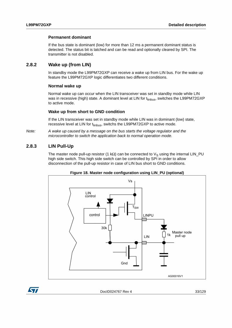
DocID024767 Rev 4 33/129
L99PM72GXP Detailed description
128
Permanent dominant
If the bus state is dominant (low) for more than 12 ms a permanent dominant status is detected. The status bit is latched and can be read and optionally cleared by SPI. The transmitter is not disabled.
2.8.2 Wake up (from LIN)
In standby mode the L99PM72GXP can receive a wake up from LIN bus. For the wake up feature the L99PM72GXP logic differentiates two different conditions.
Normal wake up
Normal wake up can occur when the LIN transceiver was set in standby mode while LIN was in recessive (high) state. A dominant level at LIN for tlinbus, switches the L99PM72GXP to active mode.
Wake up from short to GND condition
If the LIN transceiver was set in standby mode while LIN was in dominant (low) state, recessive level at LIN for tlinbus, switchs the L99PM72GXP to active mode.
Note: A wake up caused by a message on the bus starts the voltage regulator and the microcontroller to switch the application back to normal operation mode.
2.8.3 LIN Pull-Up
The master node pull-up resistor (1 kΩ) can be connected to VS using the internal LIN_PU high side switch. This high side switch can be controlled by SPI in order to allow disconnection of the pull-up resistor in case of LIN bus short to GND conditions.
Figure 18. Master node configuration using LIN_PU (optional)

Detailed description L99PM72GXP
34/129 DocID024767 Rev 4
LIN_PU high side driver characteristics:
• Activated by default and can be turned off by SPI Command (CR4)
• remains active in standby modes
• Switch off only in case of over-temperature (TSD2 = thermal shut down #2)
• no over current protection.
• Typical RDS(on), 10 Ω
2.9 High speed CAN bus transceiverGeneral requirements:
• Communication Speed up to 1Mbit/s.
• ISO 11898-2 and ISO 11898-5 compliant
• Selective wake-up functionality according to ISO 11898-6
• Non-selective wake-up functionality according to ISO 11898-5
• SAE J2284 compliant
• Function range from -27 V to 40 V DC at CAN pins.
• GND disconnection fail safe at module level.
• GND shift operation at system level.
• Microcontroller Interface with CMOS compatible I/O pins.
• ESD and transient immunity according to ISO7637 and EN / IEC61000-4-2
• Matched output slopes and propagation delay
• Receive-only mode available
For further reducing the current consumption in standby mode, the integrated CAN bus interface offers an ultra-low current consumption.

DocID024767 Rev 4 35/129
L99PM72GXP Detailed description
128
2.9.1 CAN transceiver operating modes
Figure 19. Transceiver state diagram if selective wake-up is disabled (CR16 SW_EN = 0)
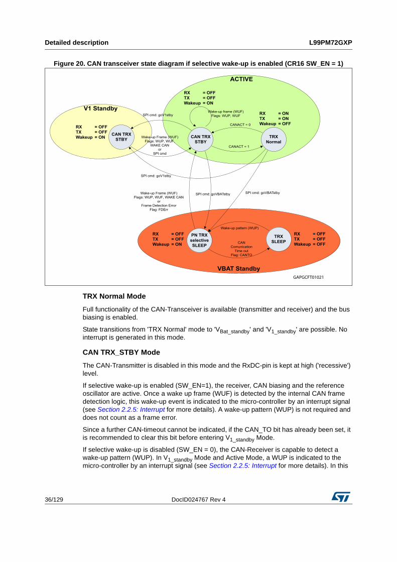
Detailed description L99PM72GXP
36/129 DocID024767 Rev 4
Figure 20. CAN transceiver state diagram if selective wake-up is enabled (CR16 SW_EN = 1)
TRX Normal Mode
Full functionality of the CAN-Transceiver is available (transmitter and receiver) and the bus biasing is enabled.
State transitions from 'TRX Normal' mode to 'VBat_standby' and 'V1_standby' are possible. No interrupt is generated in this mode.
CAN TRX_STBY Mode
The CAN-Transmitter is disabled in this mode and the RxDC-pin is kept at high ('recessive') level.
If selective wake-up is enabled (SW_EN=1), the receiver, CAN biasing and the reference oscillator are active. Once a wake up frame (WUF) is detected by the internal CAN frame detection logic, this wake-up event is indicated to the micro-controller by an interrupt signal (see Section 2.2.5: Interrupt for more details). A wake-up pattern (WUP) is not required and does not count as a frame error.
Since a further CAN-timeout cannot be indicated, if the CAN_TO bit has already been set, it is recommended to clear this bit before entering V1_standby Mode.
If selective wake-up is disabled (SW_EN = 0), the CAN-Receiver is capable to detect a wake-up pattern (WUP). In V1_standby Mode and Active Mode, a WUP is indicated to the micro-controller by an interrupt signal (see Section 2.2.5: Interrupt for more details). In this

DocID024767 Rev 4 37/129
L99PM72GXP Detailed description
128
mode (SW_EN = 0) the automatic voltage biasing is disabled and the transceiver biasing works according to ISO 11898-5.
There is no automatic state transition into TRX Normal Mode in case of a detected CAN wake-up (WUF or WUP). After serving the interrupt the micro controller can initiate a state transition into TRX Normal Mode by setting the SPI bit CAN_ACT to '1'.
TRX_SLEEP (SW_EN=1)
The CAN and LIN Transceivers are disabled. The CAN selective wakeup reference oscillator is off, while the receiver is in low power mode.
After the detection of CAN communication (WUP), the transceiver enters 'PN_TRX_selective_sleep' mode, starts the oscillator and decodes the CAN frame.
'TRX_SLEEP' mode is entered automatically after a CAN communication timeout.
PN TRX Selective Sleep (SW_EN=1)
In this mode the CAN frame detection logic is enabled (receiver and reference oscillator enabled). In case of receiving a wake up frame (WUF) a state transition to 'CAN TRX_STBY' is done. After the biasing has been switched on, not more than four CAN frames are ignored before a wake-up frame is recognized and the device wakes up.
If there is no CAN communication and the CAN bus is recessive for longer than tsilence, an automatic state transition to 'TRX_SLEEP' is done.
In case of a Frame-Detect-Error (SR4, FDERR=1), an automatic wake up is performed and the selective wakeup feature is disabled (SW_EN=0).
Oscillator monitoring
While selective wake-up is enabled, a timer is started with each recessive to dominant edge.
If after the expiration of 300 µs on this timer less than 6 recessive bits are counted, an oscillator fail is detected and the osc_mon bit is set to '1'. Subsequently the device enters wake-up mode according to ISO11898-5 (wake-up pattern wake-up).
2.9.2 Sequence for enabling selective wakeup
After power-on reset the selective wakeup feature is disabled.
The Configuration Registers 7 to 15 have to be read and verified by the microcontroller in order to ensure a valid configuration. A read operation to Registers 7 to 15 is required to allow enabling the selective wake-up feature (set SW_EN=1).
A valid read operation is indicated by the SW_RDxx bits in SR 4. The SW_RDxx bits are reset to 0 with every WRITE operation.
When all SW_RD bits are set, the SW_EN bit in CR 16 can be set to enable the Selective Wakeup function. In case the SYSERROR bit in SR 4 is set while Selective Wakeup is enabled, the Selective Wakeup is automatically disabled. In case SYSERROR is set, enabling the Selective Wakeup function is prohibited.
2.9.3 CAN error handling
The L99PM72GXP provides the following four error handling features.

Detailed description L99PM72GXP
38/129 DocID024767 Rev 4
After power-on reset (VS > VPOR) the CAN transceiver is disabled. The transceiver is enabled by setting the CAN_ACT bit in Control Register 4.
The CAN transmitter is disabled automatically in case of the following errors:
• Dominant TxDC time out
• CAN permanent recessive
• RxDC permanent recessive
• Thermal shutdown 1
The CAN receiver is not disabled in case of any failure condition.
Dominant TxDC time out
If TXDC is in dominant state (low) for t > tdom(TxD) the transmitter is disabled, status bit is latched and can be read and optionally cleared by SPI. The transmitter remains disabled until the status register is cleared.
CAN permanent recessive
If TXDC changes to dominant (low) state but CAN bus does not follow for 4 times, the transmitter is disabled, status bit is latched and can be read and optionally cleared by SPI. The transmitter remains disabled until the status register is cleared.
CAN permanent dominant
If the bus state is dominant (low) for t > tCAN a permanent dominant status is detected. The status bit is latched and can be read and optionally cleared by SPI. The transmitter is not disabled.
RXDC permanent recessive
If RXDC pin is clamped to recessive (high) state, the controller is not able to recognize a bus dominant state and could start messages at any time, which results in disturbing the overall bus communication. Therefore, if RXDC does not follow TXDC for 4 times the transmitter is disabled. The status bit is latched and can be read and optionally cleared by SPI. The transmitter remains disabled until the status register is cleared.
2.9.4 Wake up by CAN
The L99PM72GXP supports 2 wakeup modes. The selective wakeup according to ISO 11898-6 or the wakeup by any bus activity according to ISO 11898-2/-5. The wake up behavior can be configured by SPI (see Chapter 6: ST SPI).
Wake up by CAN pattern (WUP)
The default setting for the wake up behavior after power-on reset is the wake up by regular communication on the CAN bus. When the CAN transceiver is in a Standby Mode (CAN TRX_STBY or TRX_SLEEP) the device can be woken up by sending two consecutive dominant bits separated by a recessive bit.
Normal pattern wake up can occur when CAN pattern wake up option is enabled and the CAN transceiver was set in Standby Mode (CAN TRX_STBY or TRX_SLEEP) while CAN

DocID024767 Rev 4 39/129
L99PM72GXP Detailed description
128
bus was in recessive (high) state or dominant (low) state. In order to wake up the L99PM72GXP, the following criteria must be fulfilled:
• The CAN interface wake-up receiver must receive a series of two consecutive valid dominant pulses, each of which must be longer than tfilter
• The distance between 2 pulses must be longer than tfilter
• The two pulses must occur within a time frame of 1.0 ms
Note: A wake up caused by a message on the bus starts the voltage regulator and the microcontroller to switch the application back to normal operation mode.
Figure 21. CAN wake up capabilities
Note: Pictures above illustrate the wake up behaviour from V1_standby Mode. For wake up from VBat_standby Mode the NRESET signal (with 2 ms timing) is generated instead of the RXDL(Interrupt) signal.
Wakeup by CAN Frame (WUF)
Wake from CAN TRX_STBY
If the CAN transceiver is in STBY the CAN frame detection logic is active.
In case of a valid wake up frame the Interrupt on pin RxDC is generated and the WUF flag for wake up identification is set. There is no automatic state transition from CAN Transceiver point of view. After serving the interrupt the micro can bring the CAN Transceiver into TRX_NORMAL by setting CAN_ACT = 1 (CR 4).
Wake up from TRX_SLEEP
If the CAN Transceiver is in TRX_SLEEP mode the CAN frame detection logic is disabled. The wake up can be done in two steps. To enable the CAN frame detection logic a wake up

Detailed description L99PM72GXP
40/129 DocID024767 Rev 4
pattern must be sent on the bus. With the detection of the wake up pattern an automatic state transition to ‘PN_TRX_Selective_Sleep’ state is done. WUP flag is set.
In ‘PN_TRX_Selective_Sleep’ the CAN frame detection logic is enabled. If a valid wake up frame is detected a state transition to TRX_STBY is done, the WUF flag is set and the micro is powered up. The remote transition request bit is ignored in wake-up frames. Also masking of the data length code (DLC) bits is not supported.
After expiration of the frame error counter (FEC), a wake up is performed and the selective wakeup feature is disabled.
The frame-error-counter (FEC) is cleared after each expiration of the time tsilence whenever the frame detection logic is enabled.
2.9.5 CAN receive only mode
With the CAN_rec_only bit in Control register 4 it is possible to disable the CAN Transmitter in active mode. In this mode it is possible to listen to the bus but not sending to it. The Receiver termination network is still activated in this mode.
2.9.6 CAN looping mode
If the CAN_Loop_en bit in Control register 4 is set the TxDC input is mapped directly to the RxDC pin. This mode can be used in combination with the CAN Receive only mode, to run diagnosis for the CAN protocol handler of the micro controller.
2.10 Serial Peripheral Interface (ST SPI Standard 3.0)A 24 bit SPI is used for bi-directional communication with the micro controller.
During active mode, the SPI
• triggers the watchdog
• controls the modes and status of all L99PM72GXP modules (incl. input and output drivers)
• provides driver output diagnostic
• provide L99PM72GXP diagnostic (incl. over temperature warning, L99PM72GXP operation status)
The SPI can be driven by a micro controller with its SPI peripheral running in following mode: CPOL = 0 and CPHA = 0.
For this mode input data is sampled by the low to high transition of the clock CLK, and output data is changed from the high to low transition of CLK.
This device is not limited to micro controller with a built-in SPI. Only three CMOS-compatible output pins and one input pin are needed to communicate with the device. A fault condition can be detected by setting CSN to low. If CSN = 0, the DO pin reflects the global error flag (fault condition) of the device.
Chip Select Not (CSN)
The input pin is used to select the serial interface of this device. When CSN is high, the output pin (DO) is in high impedance state. A low signal activates the output driver and a

DocID024767 Rev 4 41/129
L99PM72GXP Detailed description
128
serial communication can be started. The state during CSN = 0 is called a communication frame.
If CSN = low for t > tCSNfail the DO output is switched to high impedance in order to not block the signal line for other SPI nodes.
Serial Data In (DI)
The input pin is used to transfer data serial into the device. The data applied to the DI are sampled at the rising edge of the CLK signal and shifted into an internal 24 bit shift register. At the rising edge of the CSN signal the contents of the shift register is transferred to Data Input Register. The writing to the selected Data Input Register is only enabled if exactly 24 bits are transmitted within one communication frame (i.e. CSN low). If more or less clock pulses are counted within one frame the complete frame is ignored. This safety function is implemented to avoid an activation of the output stages by a wrong communication frame.
Note: Due to this safety functionality a daisy chaining of SPI is not possible. Instead, a parallel operation of the SPI bus by controlling the CSN signal of the connected IC's is recommended.
Serial Data Out (DO)
The data output driver is activated by a logical low level at the CSN input and goes from high impedance to a low or high level depending on the global error flag (fault condition). The first rising edge of the CLK input after a high to low transition of the CSN pin transfers the content of the selected status register into the data out shift register. Each subsequent falling edge of the CLK shifts the next bit out.
Serial Clock (CLK)
The CLK input is used to synchronize the input and output serial bit streams. The data input (DI) is sampled at the rising edge of the CLK and the data output (DO) changes with the falling edge of the CLK signal. The SPI can be driven with a CLK Frequency up to 1 MHz.

Protection and diagnosis L99PM72GXP
42/129 DocID024767 Rev 4
3 Protection and diagnosis
3.1 Power supply failOvervoltage and undervoltage detection on VS
3.1.1 VS overvoltage
If the supply voltage VS reaches the over voltage threshold (VSOV):
• Outputs OUTx, RELx and LIN are switched to high impedance state (load protection). CAN is not disabled. Recovery of outputs when the overvoltage condition disappears is depending on the setting of VLOCK_OUT_EN bit in Control Register 4.
– VLOCK_OUT_EN = 1: Outputs are off until read and clear SR3.
– VLOCK_OUT_EN = 0: Outputs switch automatically on when overvoltage condition disappears.
• The over voltage bit is set and can be cleared with a ‘Read and Clear’ command. The overvoltage bit is removed automatically if VLOCK_OUT_EN = 0 and the overvoltage condition disappears.
• Outputs REL1,2 can be excluded from a shutdown in case of overvoltage by SPI (LS_OV/UV_shutdown_en in CR4)
3.1.2 VS undervoltage
If the supply voltage VS drops below the under voltage threshold voltage (VSUV)
• Outputs OUTx, RELx and LIN are switched to high impedance state (load protection). CAN is not disabled. Recovery of outputs when the undervoltage condition disappears is depending on the setting of VLOCK_OUT_EN bit.
– VLOCK_OUT_EN = 1: Outputs are off until read and clear SR3.
– VLOCK_OUT_EN = 0: Outputs switch on automatically when undervoltage condition disappears.
• The undervoltage bit is set and can be cleared with a ‘Read and Clear’ command. The undervoltage bit is removed automatically if VLOCK_OUT_EN = 0 and the undervoltage condition disappears
• Outputs REL1,2 can be excluded from a shutdown in case of undervoltage by SPI (LS_OV/UV_shutdown_en in CR4)

DocID024767 Rev 4 43/129
L99PM72GXP Protection and diagnosis
128
Figure 22. Overvoltage and undervoltage protection and diagnosis

Protection and diagnosis L99PM72GXP
44/129 DocID024767 Rev 4
3.2 Temperature warning and thermal shut-down
Figure 23. Thermal shutdown protection and diagnosis
Note: The Thermal State machine recovers the same state were it was before entering Standby Mode. In case of a TSD2 it enters TSD1 state.

DocID024767 Rev 4 45/129
L99PM72GXP Protection and diagnosis
128
3.3 High side driver outputsThe component provides a total of 4 high side outputs Out1...4, (7 Ω typ. at 25°C) to drive e.g. LED's or hall sensors and 1 high side output OUT_HS with 1 Ω typ. at 25°C).
• The high side outputs switch off in case of:
• VS overvoltage and undervoltage
• Overcurrent
• Overtemperature (TSD1) with pre warning(c)
In case of overcurrent or overtemperature (TSD1) condition, the drivers switch off. The according status bit is latched and can be read and optionally cleared by SPI. The drivers remain off until the status is cleared.
In case overvoltage or undervoltage condition, the drivers are switched off. The according status bit is latched and can be read and optionally cleared by SPI. If the VLOCK_OUT_EN bit (Control Register 4) is set to ‘1’ the drivers remain off until the status is cleared. If the VLOCK_OUT_EN bit is set to ‘0’ the drivers switch on automatically if the error condition disappears.
In case of open load condition, the according status register is latched. The status can be read and optionally cleared by SPI. The High sides are not switched off.
For OUT_HS the auto recovery feature (OUTHS_rec_en bit Control Register 4) can be enabled. If this bit is set to ‘1’ the driver automatically restarts from a overload condition. This overload recovery feature is intended for loads which have an initial current higher than the over current limit of the output (e.g. Inrush current of cold light bulbs). During auto recovery mode the over current status bit can not be read from SPI.
The device itself cannot distinguish between a real overload and a non linear load like a light bulb. A real overload condition can only be qualified by time. As an example, the micro controller can switch on light bulbs by setting the over current recovery bit for the first 50 ms. After clearing the recovery bit, the output is automatically disabled if the overload condition still exists.
In case of a fail safe condition, the high side drivers are switched off. The control bits are set to default values. (except OUT3/FSO if it is used as a High Side Driver Output)
Note: The maximum voltage and current applied to the High Side Outputs is specified in 2.1 ‘Absolute Maximum Ratings’. Appropriate external protection may be required in order to respect these limits under application conditions.
Each high side driver can be driven whether with a PWM signal or with a internal Timer (see Table 8).
For more details please refer to Section 6.2.3: Control Register 1
c. Except OUT3 when configured as FSO
Table 8. PWM configuration for high-side outputs
High side output PWM channel Internal timer
OUT1 PWM 1 Timer 1
OUT2 PWM 2 Timer 2

Protection and diagnosis L99PM72GXP
46/129 DocID024767 Rev 4
The PWM 1/3 channels start a PWM period with the ON phase, while the PWM 2/4 channels start with the OFF phase. In this way it is possible to use the 4 PWM channels in a phase shifted way. The picture below shows this feature with a duty cycle of 25% for both PWM channels.
Figure 24. Phase shifted PWM
3.4 Low side driver outputs REL1, REL2The outputs REL1, REL2 (RDSon = 2 Ω typ. @25 °C) are specially designed to drive relay loads.
The outputs provide an active output zener clamping (45 V typ.) feature for the demagnetization of the relay coil, even though a load dump condition exists.
For Fail_safe reasons the relay drivers are linked with the fail safe operation: In case of entering the Fail Safe Mode, the relay drivers switch off and the SPI control bits are set to default (i.e. driver is off).
The low side drivers switch off in case of:
• VS overvoltage and undervoltage
• Overcurrent
• Overtemperature with pre warning
OUT3 PWM 3 -
OUT4 PWM 4 Timer 2
OUTHS PWM 3 / PWM 4 Timer 1 / Timer 2
Table 8. PWM configuration for high-side outputs (continued)
High side output PWM channel Internal timer

DocID024767 Rev 4 47/129
L99PM72GXP Protection and diagnosis
128
In case of overload or overtemperature (TSD1) condition, the drivers switch off. The according status bit is latched and can be read and optionally cleared by SPI. The drivers remain off until the status is cleared.
In case VS overvoltage or undervoltage condition, the drivers are switched off. The according status bit is latched and can be read and optionally cleared by SPI. If the VLOCK_OUT_EN bit (Control Register 4) is set to ‘1’ the drivers remain off until the status is cleared. If the VLOCK_OUT_EN bit is set to ‘0’ the drivers are switched on automatically if the error condition disappears.
With the LS_OV/UV_shutdown_en bit (Control Register 4) the drivers can be excluded from a switch off in case of VS overvoltage or undervoltage. If the bit is set to ‘1’ the driver switches off, otherwise the drivers remain on.
3.5 SPI diagnosisDigital diagnosis features are provided by SPI (for details please refer to Section 6.2: SPI registers)
• V1 reset threshold programmable
• Overtemperature including. pre warning
• Open load separately for each output stage except REL1/REL2
• Overload status separately for each output stage
• VS-supply overvoltage/undervoltage
• V1 and V2 fail bit
• V2 output short to GND
• Status of the WU1...3
• Wake-up sources (CAN, LIN, SPI, Timer, WU1…3)
• Chip reset bit (start from power-on reset)
• Number of unsuccessful V1 restarts after thermal shutdown
• Number of sequential watchdog failures
• LIN diagnosis (permanent recessive/dominant, dominant TxD)
• CAN diagnosis (permanent recessive/dominant, dominant TxD, recessive RXD)
• Device State (wake-up from V1_standby or Vbat_standby)
• Forced Vbat_standby after WD-fail, forced Vbat_standby after overtemperature
• Watchdog timer state (diagnosis of watchdog)
• Failsafe status
• SPI communication error
• Diagnosis of selective wake functionality according to ISO 11898-6

Typical application L99PM72GXP
48/129 DocID024767 Rev 4
4 Typical application
Figure 25. Typical application diagram
1. In case a LIN/CAN conformance test has to be executed on the device, some capacitances have to be placed on the Fixed-Function-Unit pins: - 22 nF (low ESR and close to the pin) for all power outputs (OUT_HS, OUT1 … 4, REL1 and REL2) and
also for the wake-up inputs, if they go out of the PCB.- 47 µF and a 100 nF low ESR capacitance (close to the pin) at the power supply VS.
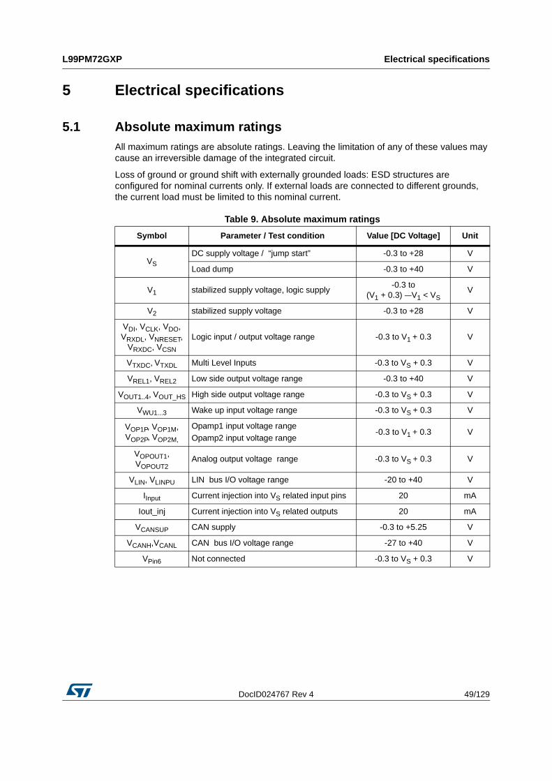
DocID024767 Rev 4 49/129
L99PM72GXP Electrical specifications
128
5 Electrical specifications
5.1 Absolute maximum ratingsAll maximum ratings are absolute ratings. Leaving the limitation of any of these values may cause an irreversible damage of the integrated circuit.
Loss of ground or ground shift with externally grounded loads: ESD structures are configured for nominal currents only. If external loads are connected to different grounds, the current load must be limited to this nominal current.
Table 9. Absolute maximum ratings
Symbol Parameter / Test condition Value [DC Voltage] Unit
VS
DC supply voltage / “jump start” -0.3 to +28 V
Load dump -0.3 to +40 V
V1 stabilized supply voltage, logic supply-0.3 to
(V1 + 0.3) V1 < VSV
V2 stabilized supply voltage -0.3 to +28 V
VDI, VCLK, VDO, VRXDL, VNRESET,
VRXDC, VCSN
Logic input / output voltage range -0.3 to V1 + 0.3 V
VTXDC, VTXDL Multi Level Inputs -0.3 to VS + 0.3 V
VREL1, VREL2 Low side output voltage range -0.3 to +40 V
VOUT1..4, VOUT_HS High side output voltage range -0.3 to VS + 0.3 V
VWU1...3 Wake up input voltage range -0.3 to VS + 0.3 V
VOP1P, VOP1M, VOP2P, VOP2M,
Opamp1 input voltage rangeOpamp2 input voltage range
-0.3 to V1 + 0.3 V
VOPOUT1, VOPOUT2
Analog output voltage range -0.3 to VS + 0.3 V
VLIN, VLINPU LIN bus I/O voltage range -20 to +40 V
IInput Current injection into VS related input pins 20 mA
Iout_inj Current injection into VS related outputs 20 mA
VCANSUP CAN supply -0.3 to +5.25 V
VCANH,VCANL CAN bus I/O voltage range -27 to +40 V
VPin6 Not connected -0.3 to VS + 0.3 V

Electrical specifications L99PM72GXP
50/129 DocID024767 Rev 4
5.2 ESD protection
5.3 Thermal data
Table 10. ESD protection
Parameter Value Unit
All pins (1)
1. HBM (Human Body Model, C = 100 pF, R = 1.5 kΩ) according to MIL 883C, Method 3015.7 or EIA/JESD22A114-A.
+/-2 kV
All output pins(2)
2. HBM with all none zapped pins grounded.
+/-4 kV
LIN +/-8 (2)
+/-10 (3)
+/-6 (4)
3. Indirect ESD test according to IEC 61000-4-2 (C = 150 pF, R = 330 Ω) and ‘Hardware Requirements for LIN, CAN and Flexray Interfaces in Automotive Applications’ (version 1.1, 2009-12-02).
4. Direct ESD test according to IEC 61000-4-2 (C = 150pF, R = 330 Ω) and ‘Hardware Requirements for LIN, CAN and Flexray Interfaces in Automotive Applications’ (version 1.1, 2009-12-02).
kV
CAN_H, CAN_L +/-8 (2)
+/-6 (4) kV
All pins (5)
5. Charged device model.
+/-500 V
Corner pins (5) +/-750 V
All pins (6)
6. Machine model: C = 200 pF; R = 0 Ω
+/-200 V
Table 11. Operating junction temperature
Symbol Parameter Value Unit
Tj Operating junction temperature -40 to 150 °C
Rthj_amb Thermal resistance junction ambient See Figure 29 K/W
Table 12. Temperature warning and thermal shutdown
Symbol Parameter Min. Typ. Max. Unit
TW_ONThermal over temperature warning threshold
Tj (1)
1. Non-overlapping.
120 130 140 °C
TSD1_OFFThermal shut-down junction temperature 1
Tj (1) 130 140 150 °C
TSD2_OFFThermal shut-down junction temperature 2
Tj (1) 150 160 170 °C
TSD12_hys Hysteresis 5 °C

DocID024767 Rev 4 51/129
L99PM72GXP Electrical specifications
128
Figure 26. Thermal data of PowerSSO-36
P ad so lde red
0
5
10
15
20
25
30
35
0.0001 0.001 0.01 0.1 1 10 100 1000
Tim e (s )
ZTH
(ºC
/W)
P ow erS S O -3 6 on 2 s 2 pP ow erS S O -3 6 on 2 s 2 p th. e nh.
P ad so lde red
0
5
10
15
20
25
30
35
0.0001 0.001 0.01 0.1 1 10 100 1000
Tim e (s )
ZTH
(ºC
/W)
P ow erS S O -3 6 on 2 s 2 pP ow erS S O -3 6 on 2 s 2 p th. e nh.
AG00022V1

Electrical specifications L99PM72GXP
52/129 DocID024767 Rev 4
5.4 Package and PCB thermal data
5.4.1 PowerSSO-36 thermal data
Figure 27. PowerSSO-36 PC board
Note: Layout condition of Rth and Zth measurements (board finish thickness 1.6 mm +/- 10% board double layer, board dimension 129x60, board Material FR4, Cu thickness 0.070 mm (front and back side), thermal vias separation 1.2 mm, thermal via diameter 0.3 mm +/- 0.08 mm, Cu thickness on vias 0.025 mm).
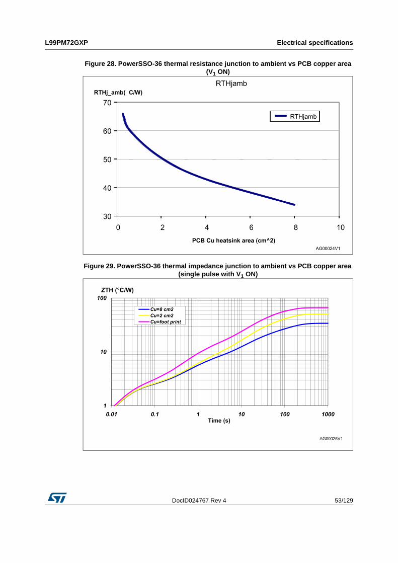
DocID024767 Rev 4 53/129
L99PM72GXP Electrical specifications
128
Figure 28. PowerSSO-36 thermal resistance junction to ambient vs PCB copper area (V1 ON)
Figure 29. PowerSSO-36 thermal impedance junction to ambient vs PCB copper area (single pulse with V1 ON)
100ZTH (°C/W)
Cu=8 cm2Cu=2 cm2
10
100ZTH (°C/W)
Cu=8 cm2Cu=2 cm2Cu=foot print
10
100ZTH (°C/W)
Cu=8 cm2Cu=2 cm2Cu=foot print
1
10
100
0.01 0.1 1 10 100 1000
ZTH (°C/W)
Time (s)
Cu=8 cm2Cu=2 cm2Cu=foot print
1
10
100
0.01 0.1 1 10 100 1000
ZTH (°C/W)
Time (s)
Cu=8 cm2Cu=2 cm2Cu=foot print
AG00025V1

Electrical specifications L99PM72GXP
54/129 DocID024767 Rev 4
Figure 30. PowerSSO-36 thermal fitting model (V1 ON)
Equation 1: pulse calculation formula
Table 13. Thermal parameter
Area/island (cm2) Footprint 2 8
R1 (°C/W) 2
R2 (°C/W) 8 4 4
R3 (°C/W) 20 15.5 10
R4 (°C/W) 36 29 18
C1 (W.s/°C) 0.01
C2 (W.s/°C) 0.1 0.2 0.2
C3 (W.s/°C) 0.8 1 1.5
C4 (W.s/°C) 2 3 6
ZTHδ RTH δ ZTHtp 1 δ–( )+⋅=
where δ tp T⁄=

DocID024767 Rev 4 55/129
L99PM72GXP Electrical specifications
128
5.5 Electrical characteristics
5.5.1 Supply and supply monitoring
The voltages are referred to ground and currents are assumed positive, when the current flows into the pin. Tj = -40°C to 130°C, unless otherwise specified.
Table 14. Supply and supply monitoring
Symbol Parameter Test condition Min. Typ. Max. Unit
VSUV VS undervoltage threshold VS increasing / decreasing 5.11 5.81 V
Vhyst_UV VS undervoltage hysteresis 0.05 0.11 0.16 V
VSOV VS overvoltage threshold VS increasing / decreasing 18.5 22 V
Vhyst_OV VS overvoltage hysteresis hysteresis 0.5 1 1.5 V
tovuv_filtVS overvoltage /undervoltage filter time
64*Tosc
IV(act)Current consumption in active mode
VS = 12 V; TxDC = high; TxDL = high; V1 = ON; V2 = ON; HS/LS Driver OFF
6 12 mA
IV(BAT)Current consumption in VBat_standby mode(1)
1. Conditions for specified current consumption:VLIN > (VS - 1.5 V)(CAN_H – CAN_L) < 0.4 V or (CAN_H – CAN_L) > 1.2 VVWU < 1 V or VWU > (Vs – 1.5V)The current consumption in standby modes with cyclic sense can be calculated using the following formulas:IV(BAT)CS = IV(BAT) + 55 µA + (2 mA * (tON + 100 µs) / T)I(V1)CS = IV1 + 55 µA + (2 mA * (tON + 100 µs) / T)
VS = 12V; both voltage regulators deactivated; HS/LS driver OFF; no CAN communication
8 12 28 µA
IV(BAT)CS
Current consumption in VBat_standby mode with cyclic sense enabled(1)
VS = 12 V; both voltage regulators deactivated; T = 50 ms; tON = 100 µs
40 75 125 µA
IV(BAT)CW
Current consumption in VBat_standby mode with cyclic wake enabled(1)
VS = 12 V; both voltage regulators deactivated during standby phase
40 75 125 µA
IV(V1stby)Current consumption in V1_standby mode(1)
VS = 12 V; voltage regulator V1 active (IV1 < ICMP); HS/LS driver OFF
16 51 76 µA
IV(SW)
Current consumption in standby mode but selective wakeup enabled and CAN communication on the bus (PN_TRX_selective_Sleep) (1)
VS = 12 V; both voltage regulators deactivated; HS/LS driver OFF
1200 µA
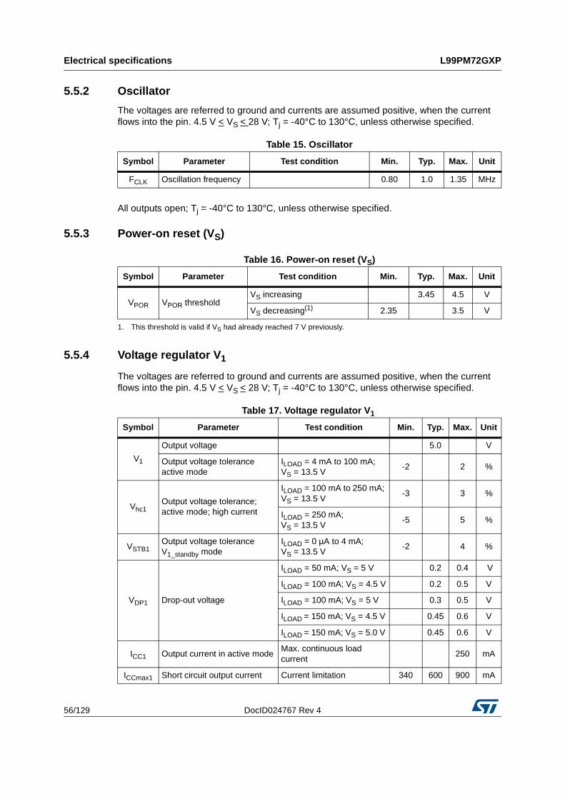
Electrical specifications L99PM72GXP
56/129 DocID024767 Rev 4
5.5.2 Oscillator
The voltages are referred to ground and currents are assumed positive, when the current flows into the pin. 4.5 V < VS < 28 V; Tj = -40°C to 130°C, unless otherwise specified.
All outputs open; Tj = -40°C to 130°C, unless otherwise specified.
5.5.3 Power-on reset (VS)
5.5.4 Voltage regulator V1
The voltages are referred to ground and currents are assumed positive, when the current flows into the pin. 4.5 V < VS < 28 V; Tj = -40°C to 130°C, unless otherwise specified.
Table 15. Oscillator
Symbol Parameter Test condition Min. Typ. Max. Unit
FCLK Oscillation frequency 0.80 1.0 1.35 MHz
Table 16. Power-on reset (VS)
Symbol Parameter Test condition Min. Typ. Max. Unit
VPOR VPOR threshold VS increasing 3.45 4.5 V
VS decreasing(1)
1. This threshold is valid if VS had already reached 7 V previously.
2.35 3.5 V
Table 17. Voltage regulator V1
Symbol Parameter Test condition Min. Typ. Max. Unit
V1
Output voltage 5.0 V
Output voltage tolerance active mode
ILOAD = 4 mA to 100 mA; VS = 13.5 V
-2 2 %
Vhc1Output voltage tolerance; active mode; high current
ILOAD = 100 mA to 250 mA; VS = 13.5 V
-3 3 %
ILOAD = 250 mA; VS = 13.5 V
-5 5 %
VSTB1Output voltage toleranceV1_standby mode
ILOAD = 0 µA to 4 mA; VS = 13.5 V
-2 4 %
VDP1 Drop-out voltage
ILOAD = 50 mA; VS = 5 V 0.2 0.4 V
ILOAD = 100 mA; VS = 4.5 V 0.2 0.5 V
ILOAD = 100 mA; VS = 5 V 0.3 0.5 V
ILOAD = 150 mA; VS = 4.5 V 0.45 0.6 V
ILOAD = 150 mA; VS = 5.0 V 0.45 0.6 V
ICC1 Output current in active modeMax. continuous load current
250 mA
ICCmax1 Short circuit output current Current limitation 340 600 900 mA

DocID024767 Rev 4 57/129
L99PM72GXP Electrical specifications
128
5.5.5 Voltage regulator V2
The voltages are referred to ground and currents are assumed positive, when the current flows into the pin. 4.5 V < VS < 28 V; Tj = -40°C to 130°C, unless otherwise specified.
Cload1 Load capacitor 1 Ceramic (+/- 20%) 0.22(1) µF
tTSDV1 deactivation time after thermal shutdown
1 sec
ICMP_ris Current comp. rising threshold Rising current 1.0 2.5 4.0 mA
ICMP_falCurrent comp. falling threshold
Falling current 0.8 1.95 3.1 mA
ICMP_hys Current comp. hysteresis 0.5 mA
V1fail V1 fail threshold V1 forced 2 V
tV1fail V1 fail filter time 2 µs
tV1short V1 short filter time 4 ms
1. Nominal capacitor value required for stability of the regulator. Tested with 220nF ceramic (+/- 20%). Capacitor must be located close to the regulator output pin.
Table 17. Voltage regulator V1 (continued)
Symbol Parameter Test condition Min. Typ. Max. Unit
Table 18. Voltage regulator V2
Symbol Parameter Test condition Min. Typ. Max. Unit
V2 Output voltage 5.0 V
V2
Output voltage tolerance; active mode
ILOAD = 1 mA to 50 mA; VS = 13.5 V
-3 3 %
Vhc1
Output voltage tolerance; active mode
ILOAD = 50 mA to 80 mA; VS = 13.5 V
-4 4 %
V2
Output voltage tolerance; active mode; high current
ILOAD = 100 mA; VS = 13.5 V -6 6 %
VSTB2
Output voltage toleranceV1_standby mode
ILOAD = 1 mA; VS = 13.5 V -6.5 6.5 %
VDP2 Drop-out voltage ILOAD = 25 mA; VS = 5.25 V 0.3 0.4 V
ILOAD = 50 mA; VS = 5.25 V 0.4 0.7 V
ICC2Output current in active mode
Max. continuous load current 100 mA
ICCmax2Short circuit output current
Current limitation 150 280 450 mA
Cload Load capacitor Ceramic (+/- 20%) 0.22(1) µF
V2fail V2 fail threshold V2 forced 2 V

Electrical specifications L99PM72GXP
58/129 DocID024767 Rev 4
5.5.6 Reset output
The voltages are referred to GND and currents are assumed positive, when the current flows into the pin. 4.0 V < VS < 28 V; Tj = -40°C to 130°C, unless otherwise specified.
5.5.7 Watchdog
4.5 V < VS < 28 V; 4.8 V < V1 < 5.2 V; Tj = -40°C to 130°C, unless otherwise specified, see Figure 31 and Figure 32.
tV2fail V2 fail filter time 2 µs
tV2short V2 short filter time 4 ms
1. Nominal capacitor value required for stability of the regulator. Tested with 220 nF ceramic (+/- 20%). Capacitor must be located close to the regulator output pin
Table 18. Voltage regulator V2 (continued)
Symbol Parameter Test condition Min. Typ. Max. Unit
Table 19. Reset output
Symbol Parameter Test condition Min. Typ. Max. Unit
VRT1 Reset threshold voltage 1 VV1 decreasing 3.7 3.9 4.1 V
VRT2 Reset threshold voltage 2 VV1 decreasing 4.2 4.3 4.45 V
VRT3 Reset threshold voltage 3 VV1 decreasing 4.25 4.4 4.55 V
VRT4 Reset threshold voltage 4VV1 decreasing 4.5 4.60 4.75 V
VV1 increasing 4.7 4.8 4.9 V
VRESETReset pin low output voltage
V1 > 1 V; IRESET = 5 mA 0.2 0.4 V
RRESET Reset pull up int. resistor 80 110 150 kΩ
tRR Reset reaction time ILOAD = 1 mA 6 40 μs
tUV1 V1 undervoltage filter time 16 μs
Trd Reset pulse duration 1.46 2.0 2.5 ms
Table 20. Watchdog
Symbol Parameter Test condition Min. Typ. Max. Unit
tLW Long open window 48.75 65 81.25 ms
TEFW1 Early failure window 1 4.5 ms
TLFW1 Late failure window 1 20 ms
TSW1 Safe window 1 7.5 12 ms
TEFW2 Early failure window 2 22.3 ms
TLFW2 Late failure window 2 100 ms
TSW2 Safe window 2 37.5 60 ms
TEFW3 Early failure window 3 45 ms

DocID024767 Rev 4 59/129
L99PM72GXP Electrical specifications
128
Figure 31. Watchdog timing (long, early, late and safe window)
TLFW3 Late failure window 3 200 ms
TSW3 Safe window 3 75 120 ms
TEFW4 Early failure window 4 90 ms
TLFW4 Late failure window 4 400 ms
TSW4 Safe window 4 150 240 ms
Table 20. Watchdog (continued)
Symbol Parameter Test condition Min. Typ. Max. Unit

Electrical specifications L99PM72GXP
60/129 DocID024767 Rev 4
Figure 32. Watchdog early, late and safe windows
5.5.8 High side outputs
The voltages are referred to GND and currents are assumed positive, when the current flows into the pin. 6 V < VS < 18 V; 4.8 V < V1 < 5.2 V; Tj = -40°C to 130°C, unless otherwise specified.
Table 21. Output (OUT_HS)
Symbol Parameter Test condition Min. Typ. Max. Unit
RDS(on)
Static drain source on-resistance (IOUT_HS = 150 mA)
Tj = 25°C 1.0 2.0 Ω
Tj = 125°C 1.6 3 Ω
td(on) Switch on delay time 0.2 VS 5 35 60 µs
td(off) Switch off delay time 0.8 VS 40 95 150 µs
tSCF Short circuit filter time Tested by scan chain 64 * TOSC
td_ARHS Auto recovery filter time Tested by scan chain 400 * TOSC
dVOUT/dt Slew rate 0.18 0.5 0.8 V/µs
IOUTShort circuit shut down current
480 900 1320 mA
IOLD Open load detection current 40 80 120 mA
tOLDT Open load detection time Tested by scan chain 64 * TOSC
IFW (1)
1. Parameter guaranteed by design.
Loss of GND current (ESD structure)
100 mA

DocID024767 Rev 4 61/129
L99PM72GXP Electrical specifications
128
5.5.9 Relay drivers
The voltages are referred to GND and currents are assumed positive, when the current flows into the pin. 6 V < VS < 18 V; 4.8 V < V1 < 5.2 V; Tj = -40 to 130°C, unless otherwise specified.
Table 22. Outputs (OUT1...4)
Symbol Parameter Test condition Min. Typ. Max. Unit
RDS(ON)
Static drain source on-resistance (IOUT_HS = 150 mA)
ILOAD = 60 mA; Tj = 25°C 7 13 Ω
IOUTShort circuit shut down current
8 V < VS < 16 V 140 235 350 mA
IOLD Open load detection current 0.9 2 4.5 mA
dVOUT/dt Slew rate 0.2 0.5 0.8 V/µs
td(on) Switch ON delay time 0.2 VS 5 35 60 µs
td(off) Switch OFF delay time 0.8 VS 30 95 150 µs
tSCF Short circuit filter time Tested by scan chain 64 * TOSC
IFW (1)
1. Parameter guaranteed by design.
Loss of GND current (ESD structure)
100 mA
tOLDT Open load detection time Tested by scan chain 64 * TOSC
Table 23. Relay drivers
Symbol Parameter Test condition Min. Typ. Max. Unit
RDS(on) DC output resistance ILOAD = 100 mA at Tj = 25°C 2 3 Ω
IOUTShort circuit shut down current
8 V < VS < 16 V 250 375 500 mA
VZOutput clamp voltage (1)
1. The output is capable to switch off relay coils with the impedance of RL = 160 Ω; L = 300 mH (RL = 220 Ω; L = 420 mH); at VS = 40 V (Load dump condition)
ILOAD = 100 mA 40 48 V
tONHLTurn on delay time to 10% VOUT
5 50 100 µs
tOFFLHTurn off delay time to 90% VOUT
5 50 100 µs
tSCF Short circuit filter time Tested by scan chain 64*TOSC
dVOUT/dt Slew rate 0.2 2 4 V/µs

Electrical specifications L99PM72GXP
62/129 DocID024767 Rev 4
5.5.10 Wake up inputs (WU1 ... WU3)
The voltages are referred to GND and currents are assumed positive, when the current flows into the pin. 6 V < VS < 18 V; Tj = -40 to 130°C, unless otherwise specified.
5.5.11 High speed CAN transceiver(d)
Selective wake functionality according to ISO 11898-6
The voltages are referred to GND and currents are assumed positive, when the current flows into the pin. 6 V < VS < 18 V; 4.8 V < VCANSUP. < 5.2 V; Tjunction = -40°C to 130°C, unless otherwise specified. -12 V = (CANH + CANL) / 2 = 12 V.
Table 24. Wake-up inputs
Symbol Parameter Test condition Min. Typ. Max. Unit
VWUthpWake-up negative edge threshold voltage
0.4 VS 0.45 VS 0.5 VS V
VWUthnWake-up positive edge threshold voltage
0.5 VS 0.55 VS 0.6 VS V
VHYST Hysteresis 0.05 VS 0.1 VS 0.15 VS V
tWU_stat Static wake filter time 64 * TOSC µs
IWU_stdbyInput current in standby mode
VWU < 1 V or VWU > (VS – 1.5 V)
9 15 28 µA
RWU_act
Input resistor to GND in active mode and in standby mode during wake-up input sensing
80 160 300 kΩ
tWU_cyc Cyclic wake filter time 16 µs
d. ISO 11898-2 and ISO 11898-5 compliant.SAE J2284 compliant.
Table 25. CAN communication operating range
Symbol Parameter Test condition Min. Typ. Max. Unit
VSCOM
Supply voltage operating range for CAN communication
Active mode, V1 = VCANSUP 5.5 — 18 V
Table 26. CAN transmit data input: pin TxDC
Symbol Parameter Test condition Min. Typ. Max. Unit
VTXDCLOW Input voltage dominant level Active mode, V1 = 5 V 1.35 1.8 V
VTXDCHIGH Input voltage recessive level Active mode, V1 = 5 V 2.5 3 V
VTXDCHYS VTXDCHIGH - VTXDCLOW Active mode, V1 = 5 V 0.7 1 V
RTXDCPU TxDC pull up resistor Active Mode, V1 = 5 V 10 20 35 kΩ

DocID024767 Rev 4 63/129
L99PM72GXP Electrical specifications
128
Table 27. CAN receive data output: pin RxDC
Symbol Parameter Test condition Min. Typ. Max. Unit
VRXDCLOWOutput voltage dominant level
Active mode, V1 = 5 V; 2 mA 0.2 0.5 V
VRXDCHIGHOutput voltage recessive level
Active mode, V1 = 5 V; 2 mA 4.5 V
Table 28. CAN transmitter and receiver: pins CANH and CANL
Symbol Parameter Test condition Min. Typ. Max. Unit
VCANHdomCANH voltage level in dominant state
Active mode; VTXDC = VTXDCLOW; RL = 65 Ω; RL = 50 Ω
2.75 4.5 V
VCANLdomCANL voltage level in dominant state
Active mode; VTXDC = VTXDCLOW; RL = 65 Ω; RL = 50 Ω
0.5 2.25 V
VDIFF,domOUT
Differential output voltage in dominant state: VCANHdom -VCANLdom
Active mode; VTXDC = VTXDCLOW; RL = 65 Ω; RL = 50 Ω
1.5 3 V
VCM(1) Driver symmetry:
VCANHdom+VCANLdom
Active mode; VTXDC = VTXDCLOW; fTXDC = 250kHz; rectangular, 50% duty cycle
0.9 *VCANSUP
VCANSUP1.1 *
VCANSUPV
VCANHrec
CANH voltage level in recessive state (Normal Mode)
Active mode; VTXDC = VTXDCHIGH; No load
2 2.5 3 V
VCANLrec
CANL voltage level in recessive state (Normal Mode)
Active mode; VTXDC = VTXDCHiGH; No load
2 2.5 3 V
VCANHrecLP
CANH voltage level in recessive state (Low Power Mode)
V1_standby mode; VTXDC = VTXDCHIGH; No load
-0.1 0 0.1 V
VCANLrecLP
CANL voltage level in recessive state (Low Power Mode)
V1_standby mode; VTXDC = VTXDCHiGH; No load
-0.1 0 0.1 V
VDIFF,recOUT
Differential output voltage in recessive state (Normal Mode): VCANHrec - VCANLrec
Active mode; VTXDC = VTXDCHIGH; No load
-50 50 mV
VDIFF,recOUTLP
Differential output voltage in recessive state (Low Power Mode): VCANHrec -VCANLrec
V1_standby mode; VTXDC = VTXDCHIGH; No load
-50 50 mV

Electrical specifications L99PM72GXP
64/129 DocID024767 Rev 4
VCANHL,CMCommon mode Bus voltage
Measured with respect to the ground of each CAN node
-12 12 V
IOCANH,dom (0V)CANH output current in dominant state
Active mode; VTXDC = VTXDCLOW; VCANH = 0 V
-160 -75 -45 mA
IOCANL,dom (5V)CANL output current in dominant state
Active mode; VTXDC = VTXDCLOW; VCANL = 5 V
45 75 160 mA
IOCANH,dom (40V)CANH output current in dominant state
Active mode; VTXDC = VTXDCLOW; VCANH = 40 V; VCANL = 0 V; VS = 40 V
0 2 5 mA
IOCANL,dom (40V)CANL output current in dominant state
Active mode; VTXDC = VTXDCLOW; VCANL = 40 V; VCANH = 0 V; VS = 40 V
47 75 160 mA
Ileakage,CANH Input leakage current
Unpowered device; VBUS = 5 V;
– Vcansupply connect 0 Ω to GND
– Vcansupply connect 47 kΩ to GND(2)
-10 — 10 µA
Ileakage,CANL Input leakage current
Unpowered device; VBUS = 5 V;– Vcansupply connect
0 Ω to GND – Vcansupply connect
47 kΩ to GND(2)
-10 — 10 µA
Rin Internal resistance
Active mode & V1- standby mode; VTXDC = VTXDCHIGH; No load
20 27.5 38 kΩ
Rin,matching
Internal Resistor matching CANH,CANL
Active mode & V1_standby mode; VTXDC = VTXDCHIGH; No load; Rin(CANH) – Rin(CANL)
3 %
Rin,diffDifferential internal resistance
Active mode & V1_standby mode; VTXDC = VTXDCHIGH; No load
50 60 75 kΩ
Cin Internal capacitanceGuaranteed by design
20 40 pF
Table 28. CAN transmitter and receiver: pins CANH and CANL (continued)
Symbol Parameter Test condition Min. Typ. Max. Unit
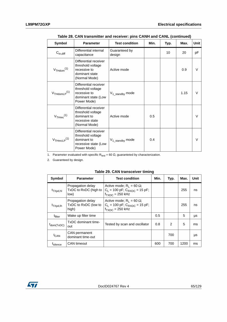
DocID024767 Rev 4 65/129
L99PM72GXP Electrical specifications
128
Cin,diffDifferential internal capacitance
Guaranteed by design
10 20 pF
VTHdom(1)
Differential receiver threshold voltage recessive to dominant state (Normal Mode)
Active mode 0.9 V
VTHdomLP(1)
Differential receiver threshold voltage recessive to dominant state (Low Power Mode)
V1_standby mode 1.15 V
VTHrec(1)
Differential receiver threshold voltage dominant to recessive state (Normal Mode)
Active mode 0.5 V
VTHrecLP(1)
Differential receiver threshold voltage dominant to recessive state (Low Power Mode)
V1_standby mode 0.4 V
1. Parameter evaluated with specific Rtest = 60 Ω, guaranteted by characterization.
2. Guaranteed by design.
Table 29. CAN transceiver timing
Symbol Parameter Test condition Min. Typ. Max. Unit
tTXpd,hl
Propagation delay TxDC to RxDC (high to low)
Active mode; RL = 60 Ω; CL = 100 pF; CRXDC = 15 pF; fTXDC = 250 kHz
255 ns
tTXpd,lh
Propagation delay TxDC to RxDC (low to high)
Active mode; RL = 60 Ω; CL = 100 pF; CRXDC = 15 pF; fTXDC = 250 kHz
255 ns
tfilter Wake up filter time 0.5 5 µs
tdom(TxDC)TxDC dominant time-out
Tested by scan and oscillator 0.8 2 5 ms
tCANCAN permanent dominant time-out
700 µs
tsilence CAN timeout 600 700 1200 ms
Table 28. CAN transmitter and receiver: pins CANH and CANL (continued)
Symbol Parameter Test condition Min. Typ. Max. Unit

Electrical specifications L99PM72GXP
66/129 DocID024767 Rev 4
tBIAS Bias reaction timeRL = 60 Ω; CL = 100 pF; CGND = 100 pF
200 µs
tV1swon
V1 switch-on time after reception of a valid WUF in VBat-standby Mode
50 µs
Table 29. CAN transceiver timing
Symbol Parameter Test condition Min. Typ. Max. Unit

DocID024767 Rev 4 67/129
L99PM72GXP Electrical specifications
128
5.5.12 LIN transceiver(e)
The voltages are referred to GND and currents are assumed positive, when the current flows into the pin. 6 V < VS < 18 V; 4.8 V < V1 < 5.2 V; Tjunction = -40°C to 130°C, unless otherwise specified.
e. LIN 2.1 compliant for Baud rates up to 20 kBit/s.SAE J2602 compatible.
Table 30. LIN transmit data input: pin TxD
Symbol Parameter Test condition Min. Typ. Max. Unit
VTXDLOW Input voltage dominant level Active mode; V1 = 5 V 1,35 1.8 V
VTXDHIGH Input voltage recessive level Active mode; V1 = 5 V 2.5 3 V
VTXDHYS VTXDHIGH - VTXDLOW Active mode; V1 = 5 V 0.7 1 V
RTXDPU TXD pull up resistor Active Mode; V1 = 5 V 10 20 35 kΩ
Table 31. LIN receive data output: pin RxD
Symbol Parameter Test condition Min. Typ. Max. Unit
VRXDLOWOutput voltage dominant level
Active mode; V1 = 5 V; 2 mA 0.2 0.5 V
VRXDHIGHOutput voltage recessive level
Active mode; V1 = 5 V; 2 mA 4.5 V
Table 32. LIN transmitter and receiver: pin LIN
Symbol Parameter Test condition Min. Typ. Max. Unit
VTHdom
Receiver threshold voltage recessive to dominant state
0.4 VS 0.45 VS 0.5 VS V
VBusdomReceiver dominant state
0.4 VS V
VTHrec
Receiver threshold voltage dominant to recessive state
0.5 *VS
0.55 *VS
0.6 *VS
V
VBusrecReceiver recessive state
0.6 VS V
VTHhys
Receiver threshold hysteresis: VTHrec -VTHdom
0.07 *VS
0.1 *VS
0.175 *VS
V
VTHcnt
Receiver tolerance center value: (VTHrec +VTHdom)/2
0.475 *VS
0.5 *VS
0.525 *VS
V
VTHwkupReceiver wakeup threshold voltage
1.0 1.5 2 V

Electrical specifications L99PM72GXP
68/129 DocID024767 Rev 4
VTHwkdwnReceiver wakeup threshold voltage
VS - 3.5 VS - 2.5 VS - 1.5 V
tlinbusDominant time for wakeup via bus
Sleep mode; Edge: rec-dom64 *
TOSCµs
ILINDomSC
Transmitter input current limit in dominant state
VTXD = VTXDLOW; VLIN = VBATMAX = 18 V
40 100 180 mA
Ibus_PAS_dom
Input leakage current at the receiver incl. pull-up resistor
VTXD = VTXDHIGH; VLIN = 0 V; VBAT = 12 V(1) -1 mA
Ibus_PAS_rec
Transmitter input current in recessive state
In stanby Modes; VTXD = VTXDHIGH; VLIN > 8 V; VBAT < 18 V; VLIN ≥ VBAT
20 µA
Ibus_NO_GNDInput current if loss of GND at Device
GND = VS; 0 V < VLIN < 18 V; VBAT = 12 V
-1 1 mA
IbusInput current if loss of VBAT at Device
GND = VS; 0 V < VLIN < 18 V 100 µA
VLINdomLIN voltage level in dominant state
Active mode; VTXD = VTXDLOW; ILIN = 40 mA
1.2 V
VLINrecLIN voltage level in recessive state
Active mode; VTXD = VTXDHIGH; ILIN = 10 µA
0.8 *VS
1 V
RLINupLIN output pull up resistor
VLIN = 0 V 20 40 60 kΩ
CLINLIN input capacitance
90 pF
1. Slave mode.
Table 33. LIN transceiver timing
Symbol Parameter Test condition Min. Typ. Max. Unit
tRXpd
Receiver propagation delay time
tRXpd = max(tRXpdr,tRXpdf); tRXpdf = t(0.5 VRXD) - t(0.45 VLIN); tRXpdr = t(0.5 VRXD) - t(0.55 VLIN); VS = 12 V; CRXD = 20 pF; Rbus = 1 kΩ; Cbus = 1 nF; Rbus = 660 Ω; Cbus = 6.8 nF; Rbus = 500 Ω; Cbus = 10 nF
6 µs
tRXpd_sym
Symmetry of receiver propagation delay time (rising vs. falling edge)
tRXpd_sym = tRXpdr - tRXpdf; VS = 12 V; Rbus = 1 kΩ; Cbus = 1 nF; CRXD = 20 pF
-2 2 µs
Table 32. LIN transmitter and receiver: pin LIN (continued)
Symbol Parameter Test condition Min. Typ. Max. Unit
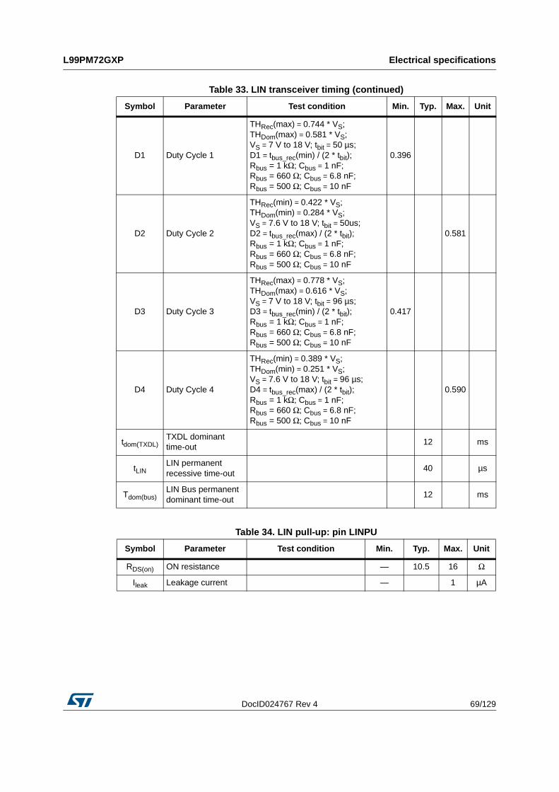
DocID024767 Rev 4 69/129
L99PM72GXP Electrical specifications
128
D1 Duty Cycle 1
THRec(max) = 0.744 * VS; THDom(max) = 0.581 * VS; VS = 7 V to 18 V; tbit = 50 µs; D1 = tbus_rec(min) / (2 * tbit); Rbus = 1 kΩ; Cbus = 1 nF; Rbus = 660 Ω; Cbus = 6.8 nF; Rbus = 500 Ω; Cbus = 10 nF
0.396
D2 Duty Cycle 2
THRec(min) = 0.422 * VS; THDom(min) = 0.284 * VS; VS = 7.6 V to 18 V; tbit = 50us; D2 = tbus_rec(max) / (2 * tbit); Rbus = 1 kΩ; Cbus = 1 nF; Rbus = 660 Ω; Cbus = 6.8 nF; Rbus = 500 Ω; Cbus = 10 nF
0.581
D3 Duty Cycle 3
THRec(max) = 0.778 * VS; THDom(max) = 0.616 * VS; VS = 7 V to 18 V; tbit = 96 µs; D3 = tbus_rec(min) / (2 * tbit); Rbus = 1 kΩ; Cbus = 1 nF; Rbus = 660 Ω; Cbus = 6.8 nF; Rbus = 500 Ω; Cbus = 10 nF
0.417
D4 Duty Cycle 4
THRec(min) = 0.389 * VS; THDom(min) = 0.251 * VS; VS = 7.6 V to 18 V; tbit = 96 µs; D4 = tbus_rec(max) / (2 * tbit); Rbus = 1 kΩ; Cbus = 1 nF; Rbus = 660 Ω; Cbus = 6.8 nF; Rbus = 500 Ω; Cbus = 10 nF
0.590
tdom(TXDL)TXDL dominant time-out
12 ms
tLINLIN permanent recessive time-out
40 µs
Tdom(bus)LIN Bus permanent dominant time-out
12 ms
Table 34. LIN pull-up: pin LINPU
Symbol Parameter Test condition Min. Typ. Max. Unit
RDS(on) ON resistance — 10.5 16 Ω
Ileak Leakage current — 1 µA
Table 33. LIN transceiver timing (continued)
Symbol Parameter Test condition Min. Typ. Max. Unit

Electrical specifications L99PM72GXP
70/129 DocID024767 Rev 4
Figure 33. LIN transmit, receive timing
5.5.13 Operational amplifier
The voltages are referred to GND and currents are assumed positive, when the current flows into the pin. 6 V < VS < 18 V; Tj = -40°C to 130°C, unless otherwise specified.
Note: The operational amplifier is on-chip stabilized for external capacitive loads CL < 25pF (all operating conditions)
Table 35. Operational amplifier
Symbol Parameter Test condition Min. Typ. Max. Unit
GBW GBW product 1 3.5 7.0 MHz
AVOLDC DC open loop gain 80 dB
PSRR Power supply rejection DC, VIN = 150 mV 80 dB
Voff Input offset voltage -5 +5 mV
VICR Common mode input range -0.2 0 3 V
VOH Output voltage range high ILOAD = 1 mA to GND VS - 0.2 VS V
VOL Output voltage range low ILOAD = 1 mA to VS 0 0.2 V
ILim+ Output current limitation + DC 10 15 30 mA
Ilim- Output current limitation - DC -10 -15 -30 mA
SR+ Slew rate positive 1 4 10 V/µs
SR- Slew rate negative -1 -4 -10 V/µs

DocID024767 Rev 4 71/129
L99PM72GXP Electrical specifications
128
5.5.14 SPI
The voltages are referred to ground and currents are assumed positive, when the current flows into the pin.
6 V < VS < 18 V; 4.5 V < V1 < 5.3 V; all outputs open; Tj = -40°C to 130°C, unless otherwise specified.
Table 36. Input: CSN
Symbol Parameter Test condition Min. Typ. Max. Unit
VCSNLOW Input voltage low level Normal mode, V1 = 5 V 1.35 1.8 V
VCSNHIGH Input voltage high level Normal mode, V1 = 5 V 2 2.9 V
VCSNHYS VCSNHIGH - VCSNLOW Normal mode, V1 = 5 V 0.6 1.0 1.5 V
ICSNPU CSN pull up resistor Normal mode, V1 = 5 V 10 20 35 kΩ
Table 37. Inputs: CLK, DI
Symbol Parameter Test condition Min. Typ. Max. Unit
tset
Delay time from standby to active mode
Switching from standby to active mode. Time until output drivers are enabled after CSN going to high.
160 300 µs
VIN L Input low level V1 = 5 V 1.35 2.05 2.75 V
VIN H Input high level V1 = 5 V 1.9 2.8 3.7 V
VIN Hyst Input hysteresis V1 = 5 V 0.4 0.75 1.5 V
I inPull down current at input
VIN = 1.5 V 5 30 60 µA
Cin (1)
1. Value of input capacity is not measured in production test. Parameter guaranteed by design.
Input capacitance at input CSN, CLK, DI and PWM1,2
0 V < V1 < 5.3 V 10 15 pF
fCLKSPI input frequency at CLK
1 MHz
Table 38. DI timing(1)
Symbol Parameter Test condition Min. Typ. Max. Unit
tCLK clock period V1 = 5 V 1000 — ns
tCLKH clock high time V1 = 5 V 400 — ns
tCLKL clock low time V1 = 5 V 400 — ns
tset CSNCSN setup time, CSN low before rising edge of CLK
V1 = 5 V 400 — ns
tset CLKCLK setup time, CLK high before rising edge of CSN
V1 = 5 V 400 — ns
tset DI DI setup time V1 = 5 V 200 — ns

Electrical specifications L99PM72GXP
72/129 DocID024767 Rev 4
thold DI DI hold time V1 = 5 V 200 — ns
tr inrise time of input signal DI, CLK, CSN
V1 = 5 V — 100 ns
tf infall time of input signal DI, CLK, CSN
V1 = 5 V — 100 ns
1. See Figure 35: SPI input timing.
Table 39. Output: DO
Symbol Parameter Test condition Min. Typ. Max. Unit
VDOL output low level V1 = 5 V; ID = -4 mA 0.5 V
VDOH output high level V = 5 V; ID = 4 mA 4.5 V
IDOLK tristate leakage current VCSN = V1; 0 V < VDO < V1 -10 10 µA
CDO tristate input capacitanceVCSN = V1; 0 V < V1 < 5.3 V(1)
1. Value of input capacity is not measured in production test. Parameter guaranteed by design.
10 15 pF
Table 40. DO timing(1)
1. See Figure 36: SPI output timing (part 1).
Symbol Parameter Test condition Min. Typ. Max. Unit
tr DO DO rise time CL = 100 pF; ILOAD = -1 mA — 50 100 ns
tf DO DO fall time CL = 100 pF; ILOAD = 1 mA — 50 100 ns
ten DO tri LDO enable time from tristate to low level
CL = 100 pF; ILOAD = 1 mA;pull-up load to V1
— 50 250 ns
tdis DO L triDO disable time from low level to tristate
CL = 100 pF; ILOAD = 4 mA; pull-up load to V1
— 50 250 ns
ten DO tri HDO enable time from tristate to high level
CL = 100 pF; ILOAD = -1 mA; pull-down load to GND
— 50 250 ns
tdis DO H triDO disable time from high level to tristate
CL = 100 pF; ILOAD = -4 mA; pull-down load to GND
— 50 250 ns
td DO DO delay timeVDO < 0.3 V1; VDO > 0.7 V1; CL = 100 pF
— 50 250 ns
Table 41. CSN timing(1)
1. See Figure 37: SPI CSN - output timing.
Symbol Parameter Test condition Min. Typ. Max. Unit
tCSN_HI,minMinimum CSN HI time, active mode
Transfer of SPI-command to Input Register
6 µs
tCSNfail CSN low timeout 20 35 50 ms
Table 38. DI timing(1) (continued)
Symbol Parameter Test condition Min. Typ. Max. Unit

DocID024767 Rev 4 73/129
L99PM72GXP Electrical specifications
128
The voltages are referred to ground and currents are assumed positive, when the current flows into the pin. 6 V < VS < 18 V; 4.8 V < V1 < 5.2 V; all outputs open; Tj = -40°C to 130°C, unless otherwise specified
5.5.15 Inputs TxDC and TxDL for Flash Mode
6 V ≤ VS ≤ 18 V; 4.5 V ≤ V1 ≤ 5.3 V; Tj = -40°C to 130°C; voltages are referred to PGND, all outputs open
Figure 34. SPI - transfer timing diagram
The SPI can be driven by a micro controller with its SPI peripheral running in following mode: CPOL = 0 and CPHA = 0.
For this mode input data is sampled by the low to high transition of the clock CLK, and output data is changed from the high to low transition of CLK.
Table 42. RXDL/NINT, RXDC/NINT timing
Symbol Parameter Test condition Min. Typ. Max. Unit
tInterupt Interrupt pulse duration — 56 — µs
Table 43. Inputs: TxDC and TxDL for Flash Mode
Symbol Parameter Test condition Min. Typ. Max. Unit
VflashLInput low level (VTXDC/L for exit from Flash Mode)
V1 = 5 V 7.1 8.4 9.0 V
VflashHInput high level (VTXDC/L for transition into Flash Mode)
V1 = 5 V 8.3 9.4 10.0 V
VflashHYS Input voltage hysteresis V1 = 5 V 0.8 1.0 1.2 V

Electrical specifications L99PM72GXP
74/129 DocID024767 Rev 4
Figure 35. SPI input timing

DocID024767 Rev 4 75/129
L99PM72GXP Electrical specifications
128
Figure 36. SPI output timing (part 1)

Electrical specifications L99PM72GXP
76/129 DocID024767 Rev 4
Figure 37. SPI CSN - output timing
Figure 38. SPI - CSN low to high transition and global status bit access
DocID024767 Rev 4 77/129
L99PM72GXP ST SPI
128
6 ST SPI
6.1 SPI communication flow
6.1.1 General description
The SPI communication is based on a standard SPI interface structure using CSN (Chip Select Not), SDI (Serial Data In), SDO (Serial Data Out/Error) and SCK (Serial Clock) signal lines.
At device start-up the master reads the <SPI-frame-ID> register (ROM address 3EH) of the slave device. This 8-bit register indicates the SPI frame length (24bit) and the availability of additional features.
Each communication frame consists of an instruction byte which is followed by two data bytes.
The data returned on SDO within the same frame always starts with the <Global Status> register. It provides general status information about the device. It is followed by two data bytes (i. e. ‘In-frame-response’).
For Write cycles the <Global Status> register is followed by the previous content of the addressed register.
For Read cycles the <Global Status> register is followed by the content of the addressed register.
A Write command is only accepted as a valid command by the device if the counted number of clocks is exact 24, otherwise the command is rejected.
Command Byte
Each communication frame starts with a command byte. It consists of an operating code which specifies the type of operation (<Write>, <Read>, <Read and Clear>, <Read Device Information>) and a 6 bit address. If less than 6 address bits are required, the remaining bits are unused but are reserved.
OCx: Operating Code
Ax: Address
Table 44. Command Byte
MSB LSB
Op Code Address
OC1 OC0 A5 A4 A3 A2 A1 A0
ST SPI L99PM72GXP
78/129 DocID024767 Rev 4
6.1.2 Operating code definition
The <Write Mode> <Read Mode> and <Read and Clear Status> operations allow access to the RAM of the device, i. e. to write to control registers or read status information.
A <Read and Clear Status> operation addressed to a device specific status register reads back and subsequently clear this status register.
A <Read and Clear Status> operation with address 3FH clears all status registers (including the Global Status Register). Configuration Register is read by this operation.
<Read Device Information> allows access to the ROM area which contains device related information such as the product family, product name, silicon version, register width and availability of a watchdog.
More detailed descriptions of the Device Information are available in ‘Read Device Information’.
6.1.3 Global Status Register
6.1.4 Configuration register(f)
The <Configuration> register is accessible at RAM address 3FH.
For the Config Register, the 8 bits are located in the low byte (LSB).
The Configuration Register is implemented for compliance purpose to ST SPI Standard.
<WD Trigger>: This Bit is reserved to serve the watchdog.
Table 45. Operating code definition
OC1 OC0 Meaning
0 0 <Write Mode>
0 1 <Read Mode>
1 0 <Read and Clear Status>
1 1 <Read Device Information>
Table 46. Global status register
Bit 7 Bit 6 Bit 5 Bit 4 Bit 3 Bit 2 Bit 1 Bit 0
Global error flag (GEF)
Comm error
Not (chip reset OR comm error)
TSD2 TSD1 V1 FailVS Fail
(OV/UV)Fail safe
f. See Section 6.2 for details.
Table 47. Configuration register
Bit 7 Bit 6 Bit 5 Bit 4 Bit 3 Bit 2 Bit 1 Bit 0
0 0 0 0 0 0 0 WD trigger

DocID024767 Rev 4 79/129
L99PM72GXP ST SPI
128
Figure 39. Read configuration register
1. The configuration register is implemented for compliance with ST standard SPI 3.0 and contains only the watchdog trigger bit at D0.
Figure 40. Write configuration register
1. The configuration register is implemented for compliance with ST standard SPI 3.0 and contains only the watchdog trigger bit at D0.

ST SPI L99PM72GXP
80/129 DocID024767 Rev 4
6.1.5 Address mapping
The RAM memory area consists of 16 bit registers.
For the device information (ROM memory area) the eight most significant bits of the memory cell are used. The remaining 8 are zero.
All unused RAM and ROM addresses are read as ‘0’.
Note: The register definition for RAM address 00H is unused. A register value of all 0 must cause the device to enter a Fail-Safe state (interpreted as ‘SDI stuck to GND’ failure).
Note: ROM address 3FH is unused. An attempt to access this address must be recognized as a communication error (‘SDI stuck to VCC’ failure) and must cause the device to enter a Fail-Safe state.
6.1.6 Write operation
The write operation starts with a Command Byte followed by 2, data bytes. The number of data bytes is specified in the <SPI-frame-ID>.
Write command format
Table 48. Address mapping
RAM Address
Description AccessROM
AddressDescription Access
3FH <Configuration> R/W 3FH Reserved N/A
… … … 3EH <SPI frame ID> R
13H Status Register 3 R
… Unused N/A
12H Status Register 2 R
11H Status Register 1 R
… … …
06H Control Register 6 R/W
05H Control Register 5 R/W
04H Control Register 4 R/W
03H Control Register 3 R/W 03H <product code 2> R
02H Control Register 2 R/W 02H <product code 1> R
01H Control Register 1 R/W 01H <silicon version> R
00H Reserved R/W 00H <ID Header> R
Table 49. Write command format: command byte
MSB LSB
Op Code Address
0 0 A5 A4 A3 A2 A1 A0
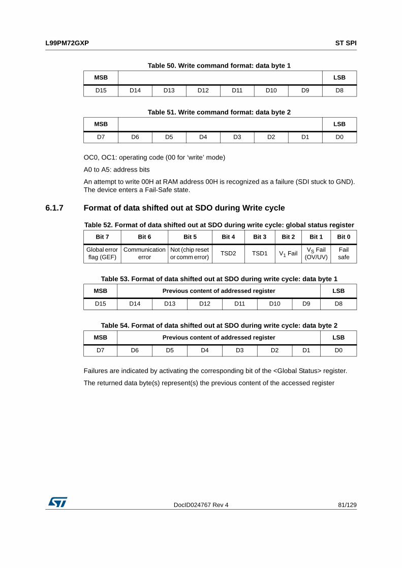
DocID024767 Rev 4 81/129
L99PM72GXP ST SPI
128
OC0, OC1: operating code (00 for ‘write’ mode)
A0 to A5: address bits
An attempt to write 00H at RAM address 00H is recognized as a failure (SDI stuck to GND). The device enters a Fail-Safe state.
6.1.7 Format of data shifted out at SDO during Write cycle
Failures are indicated by activating the corresponding bit of the <Global Status> register.
The returned data byte(s) represent(s) the previous content of the accessed register
Table 50. Write command format: data byte 1
MSB LSB
D15 D14 D13 D12 D11 D10 D9 D8
Table 51. Write command format: data byte 2
MSB LSB
D7 D6 D5 D4 D3 D2 D1 D0
Table 52. Format of data shifted out at SDO during write cycle: global status register
Bit 7 Bit 6 Bit 5 Bit 4 Bit 3 Bit 2 Bit 1 Bit 0
Global error flag (GEF)
Communication error
Not (chip reset or comm error)
TSD2 TSD1 V1 FailVS Fail
(OV/UV)Fail safe
Table 53. Format of data shifted out at SDO during write cycle: data byte 1
MSB Previous content of addressed register LSB
D15 D14 D13 D12 D11 D10 D9 D8
Table 54. Format of data shifted out at SDO during write cycle: data byte 2
MSB Previous content of addressed register LSB
D7 D6 D5 D4 D3 D2 D1 D0

ST SPI L99PM72GXP
82/129 DocID024767 Rev 4
Figure 41. Format of data shifted out at SDO during write cycle
6.1.8 Read operation
OC0, OC1: operating code (01 for ‘read’ mode)
A0 to A5: Address Bits
Table 55. Read command format: command byte
MSB LSB
Op Code Address
0 1 A5 A4 A3 A2 A1 A0
Table 56. Read command format: data byte 1
MSB LSB
0 0 0 0 0 0 0 0
Table 57. Read command format: data byte 2
MSB LSB
0 0 0 0 0 0 0 0

DocID024767 Rev 4 83/129
L99PM72GXP ST SPI
128
6.1.9 Format of data shifted out at SDO during Read cycle
Failures are indicated by activating the corresponding bit of the <Global Status> register.
The returned data byte(s) represent(s) the content of the register to be read.
Figure 42. Format of data shifted out at SDO during read cycle
Table 58. Format of data shifted out at SDO during read cycle: global status register
Bit 7 Bit 6 Bit 5 Bit 4 Bit 3 Bit 2 Bit 1 Bit 0
Global error flag (GEF)
Communication error
Not (chip reset OR comm error)
TSD2 TSD1 V1 FailVS Fail
(OV/UV)Fail safe
Table 59. Format of data shifted out at SDO during read cycle: data byte 1
MSB Previous content of addressed register LSB
D15 D14 D13 D12 D11 D10 D9 D8
Table 60. Format of data shifted out at SDO during read cycle: data byte 2
MSB Previous content of addressed register LSB
D7 D6 D5 D4 D3 D2 D1 D0

ST SPI L99PM72GXP
84/129 DocID024767 Rev 4
6.1.10 Read and Clear Status Operation
The ‘Read and Clear Status’ operation starts with a Command Byte followed 2 data bytes. The number of data bytes is specified in the <SPI-frame-ID>. The content of the data bytes is ‘don’t care’. The content of the addressed Status Register is transferred to SDO within the same frame (‘in-frame response’) and is subsequently cleared.
A ‘Read and Clear Status’ operation with address 3FH clears all Status registers (incl. the <Global Status> register). The Configuration Register is read by this operation.
OC0, OC1: operating code (10 for ‘read and clear status’ mode)
A0 to A5: address bits
Format of data shifted out at SDO during ‘Read and Clear Status’ operation
Table 61. Read and clear status command format: command byte
MSB LSB
Op Code Address
1 0 A5 A4 A3 A2 A1 A0
Table 62. Read and clear status command format: data byte 1
MSB LSB
0 0 0 0 0 0 0 0
Table 63. Read and clear status command format: data byte 2
MSB LSB
0 0 0 0 0 0 0 0
Table 64. Format of data shifted out at SDO during read and clear status: global status register
Bit 7 Bit 6 Bit 5 Bit 4 Bit 3 Bit 2 Bit 1 Bit 0
Global error flag (GEF)
Communication error
Not (chip reset OR comm error)
TSD2 TSD1 V1 FailVS Fail
(OV/UV)Fail safe
Table 65. Format of data shifted out at SDO during read and clear status: data byte 1
MSB Previous content of addressed register LSB
D15 D14 D13 D12 D11 D10 D9 D8
Table 66. Format of data shifted out at SDO during read and clear status: data byte 2
MSB Previous content of addressed register LSB
D7 D6 D5 D4 D3 D2 D1 D0

DocID024767 Rev 4 85/129
L99PM72GXP ST SPI
128
Failures are indicated by activating the corresponding bit of the <Global Status> register.
The returned data byte(s) represent(s) the content of the register to be read.
Figure 43. Format of data shifted out at SDO during read and clear status operation
6.1.11 Read device information
The device information is stored at the ROM addresses defined below and is read using the respective operating code.
Table 67. Read device information
Op CodeROM address Device information Value
OC1 OC0
1 1 3FH Reserved 00
1 1 3EH<SPI frame ID>
Includes frame width and availability of watchdog42 Hex
1 1 04H to 3DH unused 00
1 1 03H<product code 2>Unique product identifier
27h
1 1 02H<product code 1>Unique product identifier
4Bh
1 1 01H<silicon version>Indicates Design Version
05h
1 1 00H<ID Header>Device family max address of device information
43 Hex

ST SPI L99PM72GXP
86/129 DocID024767 Rev 4
The <ID-Header> (ROM address 00H) indicates the product family and specifies the highest address which contains product information
<Family Identifier>: 01 Hex (BCD)
<Highest address>: 03 Hex
The <Product Code 1> (ROM address 02H) and <Product Code 2> (ROM address 03H) represents a unique code to identify the product name.
<Product Code 1>: 4BHex
<Product Code 2>: 27 Hex
The <Silicon Version> (ROM address 01H) provides information about the silicon version according to the table below:
The <SPI-frame-ID> (ROM address 3EH) provides information about the register width (1, 2, 3 bytes) and the availability of ‘Burst Mode Read’ and watchdog.
BR: Burst-Mode read (1 = Burst-Mode read is supported)
WD: Watchdog (1 = available, 0 = not available)
32-, 24-, 16-bit: width of SPI frame
Table 68. ID-header
Bit 7 Bit 6 Bit 5 Bit 4 Bit 3 Bit 2 Bit 1 Bit 0
0 1 0 0 0 0 1 1
Family Identifier Highest address containing device information
Table 69. Family identifier
Bit 7 Bit 6 Meaning
0 0 VIPower
0 1 BCD
1 0 VIPower hybrid
1 1 —
Table 70. Silicon version identifier
Bit 7 Bit 6 Bit 5 Bit 4 Bit 3 Bit 2 Bit 1 Bit 0
Reserved Silicon version
Table 71. SPI-frame-ID
Bit 7 Bit 6 Bit 5 Bit 4 Bit 3 Bit 2 Bit 1 Bit 0
0 1 0 0 0 0 1 0
BR WD X X X 32-bit 24-bit 16-bit

DocID024767 Rev 4 87/129
L99PM72GXP ST SPI
128
<Burst Mode>: not supported
<Watchdog>: available
<Frame width>: 24 bit
6.2 SPI registers
6.2.1 Overview command byte
Table 72. SPI register: command byte
Read/write Address
x x x x x x x x
Table 73. SPI register: mode selection
Read/write Mode selection
0 0 Write
0 1 Read
1 0 Read and clear
1 1 Read device info
Table 74. SPI register: CTRL register selection
CTRL register 1…6 CTRL register selection
0 0 0 0 0 1 CTRL register1
0 0 0 0 1 0 CTRL register2
0 0 0 0 1 1 CTRL register3
0 0 0 1 0 0 CTRL register4
0 0 0 1 0 1 CTRL register5
0 0 0 1 1 0 CTRL register6
0 0 0 1 1 1 CTRL register7
0 0 1 0 0 0 CTRL register8
0 0 1 0 0 1 CTRL Register9
0 0 1 0 1 0 CTRL Register10
0 0 1 0 1 1 CTRL Register11
0 0 1 1 0 0 CTRL Register12
0 0 1 1 0 1 CTRL Register13
0 0 1 1 1 0 CTRL Register14
0 0 1 1 1 1 CTRL Register15
0 1 0 0 0 0 CTRL Register16

ST SPI L99PM72GXP
88/129 DocID024767 Rev 4
6.2.2 Overview control register
1 0 0 0 1 0 CTRL Register34
1 0 0 0 1 1 CTRL Register35
1 1 1 1 1 1 Configuration Register
Table 75. SPI register: STAT register selection
STAT register. 1…3 STAT register selection
0 1 0 0 0 1 STAT register1
0 1 0 0 1 0 STAT register2
0 1 0 0 1 1 STAT register3
0 1 0 1 0 0 STAT Register4
0 1 0 1 0 1 STAT Register5
Table 74. SPI register: CTRL register selection (continued)
CTRL register 1…6 CTRL register selection
Table 76. Overview of control register data bytes
1st data byte <15:8> 2nd data byte <7:0>
Control register 1, data
Default 0 0 0 0 0 0 0 0 0 0 0 0 0 0 0 0
Function
OU
TH
S
OU
TH
S
OU
T4
OU
T4
OU
TH
S_E
XT
OU
T3
OU
T2
OU
T1
RE
L2
RE
L1 V2 V2
Par
ity
Stb
y se
l
Go
Stb
y
Trig
Group HS control LS Output, V2 and mode control
Control register 2, data
Default 0 0 0 0 0 0 0 0 0 0 0 0 0 1 1 1
Function Reserved
WU
3_F
ilt
WU
3_F
ilt
WU
2_F
ilt
WU
2_F
ilt
WU
1_F
ilt
WU
1_F
ilt
Res
erve
d
WU
3_P
u/P
d
WU
2_P
u/P
d
WU
1_P
u/P
d
Res
erve
d
WU
3_E
N
WU
2_E
N
WU
1_E
N
Group Wake-up control Wake-up control

DocID024767 Rev 4 89/129
L99PM72GXP ST SPI
128
Control register 3, data
Default 0 0 0 0 0 0 0 0 0 0 0 0 1 1 0 0
Function
Res
erve
d
T1_
On
T1_
Per
_MS
B
T1_
Per
_LS
B
Res
erve
d
T2_
On
T2_
Per
_MS
B
T2_
Per
_LS
B
Reserved
WD
_tim
e_M
SB
WD
_tim
e_LS
B
LIN
WU
En
CA
N W
U E
n
Wak
e Ti
mer
En
Wak
e Ti
me
Sel
Group Timer Settings Watchdog and cyclic wake up settings
Control register 4, data
Default 0 0 0 1 0 1 0 0 1 1 1 0 0 0 0 0
Function
Res
erve
d
ICM
P
OU
TH
S_r
ec_e
n
VLO
CK
_OU
T_E
N
Res
erve
d
LS O
V/U
V
shut
dow
n_en
V1R
eset
_Lev
el
V1R
eset
_Lev
el
LIN
Pu
En
Res
erve
d
Lin
TxD
Tou
t En
CA
N_A
CT
CA
N_L
oop_
En
Reserved
CA
N_R
ec_O
nly
Group Control (other) Transceiver settings
Control register 5, data
Default 0 1 1 1 1 1 1 1 0 0 0 0 0 0 0 0
Function
Res
erve
d
PW
M2_
OF
F_D
C_6
PW
M2_
OF
F_D
C_5
PW
M2_
OF
F_D
C_4
PW
M2_
OF
F_D
C_3
PW
M2_
OF
F_D
C_2
PW
M2_
OF
F_D
C_1
PW
M2_
OF
F_D
C_0
PW
M F
req
PW
M1_
ON
_DC
_6
PW
M1_
ON
_DC
_5
PW
M1_
ON
_DC
_4
PW
M1_
ON
_DC
_3
PW
M1_
ON
_DC
_2
PW
M1_
ON
_DC
_1
PW
M1_
ON
_DC
_0Group PWM2 setting PWM1 setting
Control register 6, data
Default 0 1 1 1 1 1 1 1 0 0 0 0 0 0 0 0
Function
Res
erve
d
PW
M4_
OF
F_D
C_6
PW
M4_
OF
F_D
C_5
PW
M4_
OF
F_D
C_4
PW
M4_
OF
F_D
C_3
PW
M4_
OF
F_D
C_2
PW
M4_
OF
F_D
C_1
PW
M4_
OF
F_D
C_0
Res
erve
d
PW
M3_
ON
_DC
_6
PW
M3_
ON
_DC
_5
PW
M3_
ON
_DC
_4
PW
M3_
ON
_DC
_3
PW
M3_
ON
_DC
_2
PW
M3_
ON
_DC
_1
PW
M3_
ON
_DC
_0
Group PWM4 setting PWM3 setting
Table 76. Overview of control register data bytes (continued)
1st data byte <15:8> 2nd data byte <7:0>

ST SPI L99PM72GXP
90/129 DocID024767 Rev 4
Control register 7, data
Default 0 0 0 0 0 0 0 0 0 0 0 0 0 0 0 0
Function
EX
T_I
D_1
5
EX
T_I
D_1
4
EX
T_I
D_1
3
EX
T_I
D_1
2
EX
T_I
D_1
1
EX
T_I
D_1
0
EX
T_I
D_9
EX
T_I
D_8
EX
T_I
D_7
EX
T_I
D_6
EX
T_I
D_5
EX
T_I
D_4
EX
T_I
D_3
EX
T_I
D_2
EX
T_I
D_1
EX
T_I
D_0
Group Selective Wakeup Settings
Control register 8, data
Default 0 0 0 0 0 0 0 0 0 0 0 0 0 0 0 0
Function Reserved
ID_1
0
ID_9
ID_8
ID_7
ID_6
ID_5
ID_4
ID_3
ID_2
ID_1
ID_0
EX
T_I
D_1
7
EX
T_I
D_1
6
Group Selective Wakeup Settings
Control register 9, data
Default 0 0 0 0 0 0 0 0 0 0 0 0 0 0 0 0
Function ReservedC
AN
_ID
E
DLC
_3
DLC
_2
DLC
_1
DLC
_0
Group Selective Wakeup Settings
Control register 10, data
Default 0 0 0 0 0 0 0 0 0 0 0 0 0 0 0 0
Function Data Byte 2 Data Byte 1
Group Selective Wakeup Settings
Control register 11, data
Default 0 0 0 0 0 0 0 0 0 0 0 0 0 0 0 0
Function Data Byte 4 Data Byte 3
Group Selective Wakeup Settings
Control register 12, data
Default 0 0 0 0 0 0 0 0 0 0 0 0 0 0 0 0
Function Data Byte 6 Data Byte 5
Group Selective Wakeup Settings
Table 76. Overview of control register data bytes (continued)
1st data byte <15:8> 2nd data byte <7:0>

DocID024767 Rev 4 91/129
L99PM72GXP ST SPI
128
Control register 13, data
Default 0 0 0 0 0 0 0 0 0 0 0 0 0 0 0 0
Function Data Byte 8 Data Byte 7
Group Selective Wakeup Settings
Control register 14, data
Default 0 0 0 0 0 0 0 0 0 0 0 0 0 0 0 0
Function
EX
T_I
D_
Mas
k_15
EX
T_I
D_
Mas
k_14
EX
T_I
D_
Mas
k_13
EX
T_I
D_
Mas
k_12
EX
T_I
D_
Mas
k_11
EX
T_I
D_
Mas
k_10
EX
T_I
D_
Mas
k_9
EX
T_I
D_
Mas
k_8
EX
T_I
D_
Mas
k_7
EX
T_I
D_
Mas
k_6
EX
T_I
D_
Mas
k_5
EX
T_I
D_
Mas
k_4
EX
T_I
D_
Mas
k_3
EX
T_I
D_
Mas
k_2
EX
T_I
D_
Mas
k_1
EX
T_I
D_
Mas
k_0
Group Selective Wakeup Settings
Control register 15, data
Defaults 0 0 0 0 0 0 0 0 0 0 0 0 0 0 0 0
Function Reserved
ID_M
ask_
10
ID_M
ask_
9
ID_M
ask_
8
ID_M
ask_
7
ID_M
ask_
6
ID_M
ask_
5
ID_M
ask_
4
ID_M
ask_
3
ID_M
ask_
2
ID_M
ask_
1
ID_M
ask_
0
EX
T_I
D_
Mas
k_17
EX
T_I
D_
Mas
k_16
Group Selective Wakeup Settings
Control register 16, data
Defaults 0 0 0 0 0 0 0 0 0 0 0 0 0 0 0 0
Function
CR
16_3
0
CR
16_2
1
CR
16_2
0
CR
16_1
4
CR
16_1
3
CR
16_1
2
CR
16_1
1
CR
16_1
0
Res
erve
d
Sam
p 2
Sam
p 1
Sam
p 0
Res
erve
d
BR1 BR2
SW
_EN
Group Selective Wakeup Settings
Control register 34, data
Defaults 0 0 0 0 0 0 0 0 0 0 0 0 0 0 0 1
Function Reserved
WD
_EN
Control Register 35, data
Defaults 0 0 0 0 0 0 0 0 0 0 1 1 0 1 1 0
Function Reserved
CR
35_2
5
CR
35_2
4
CR
35_2
3
CR
35_2
2
CR
35_2
1
CR
35_2
0
CR
35_1
0
Table 76. Overview of control register data bytes (continued)
1st data byte <15:8> 2nd data byte <7:0>
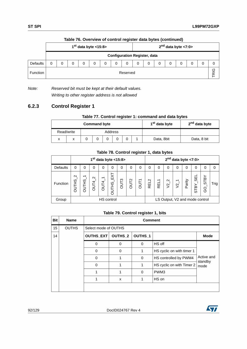
ST SPI L99PM72GXP
92/129 DocID024767 Rev 4
Note: Reserved bit must be kept at their default values.
Writing to other register address is not allowed
6.2.3 Control Register 1
Configuration Register, data
Defaults 0 0 0 0 0 0 0 0 0 0 0 0 0 0 0 0
Function Reserved
TR
IG
Table 76. Overview of control register data bytes (continued)
1st data byte <15:8> 2nd data byte <7:0>
Table 77. Control register 1: command and data bytes
Command byte 1st data byte 2nd data byte
Read/write Address
x x 0 0 0 0 0 1 Data, 8bit Data, 8 bit
Table 78. Control register 1, data bytes
1st data byte <15:8> 2nd data byte <7:0>
Defaults 0 0 0 0 0 0 0 0 0 0 0 0 0 0 0 0
Function
OU
TH
S_2
OU
TH
S_1
OU
T4_
2
OU
T4_
1
OU
TH
S_E
XT
OU
T3
OU
T2
OU
T1
RE
L2
RE
L1
V2_
2
V2_
1
Par
ity
ST
BY
_SE
L
GO
_ST
BY
Trig
Group HS control LS Output, V2 and mode control
Table 79. Control register 1, bits
Bit Name Comment
15 OUTHS Select mode of OUTHS
14 OUTHS_EXT OUTHS_2 OUTHS_1 Mode
0 0 0 HS off
Active and standby mode
0 0 1 HS cyclic on with timer 1
0 1 0 HS controlled by PWM4
0 1 1 HS cyclic on with Timer 2
1 1 0 PWM3
1 x 1 HS on

DocID024767 Rev 4 93/129
L99PM72GXP ST SPI
128
13 OUT4 Select mode of OUT4
12 OUT4_2 OUT4_1 Mode
0 0 HS off
Active and standby mode
0 1 HS on
1 0HS controlled by PWM4
1 1HS cyclic on with Timer 2
11 OUTHS_EXT Extended function of OUTHS; see OUTHS
10 OUT3 Select mode of OUT3
OUT3 Mode
0 Select FSOActive and standby mode
1Select PWM3
9 OUT2 Select mode of OUT2
OUT2 Mode
0Select PWM2 Active and
standby mode1
Select timer2
8 OUT1 Select mode of OUT1
OUT1 Mode
0Select PWM1 Active and
standby mode1
Select timer1
Table 79. Control register 1, bits (continued)
Bit Name Comment

ST SPI L99PM72GXP
94/129 DocID024767 Rev 4
7 REL2 Select mode of REL2
REL2 Mode
0 REL2 offActive and standby mode
1 REL2 onActive mode
6 REL1 Select mode of REL1
REL1 Mode
0 REL1 offActive and standby mode
1 REL1 onActive mode
5 V2
4 V2_2 V2_1
0 0 V2 OFF in all modes
0 1V2 ON in active mode; OFF in V1/VBat_standby mode
1 0V2 ON in Active/V1_standby mode; OFF in VBat_standby mode
1 1 V2 ON in all modes
3 Parity The Stby_sel and Go_stby bits are protected by a parity check
The bits Stby_sel, Go_stby and Parity must represent an even number of '1', otherwise the command is ignored and the Communication Error bit is set in the Global Status Register. Following are the valid settings
Parity STBY_SEL GO_STBY Command
0 1 1 Go to V1_standby
1 0 1 Go to VBat_standby
0 0 0 No transition to standby
1 1 0 No transition to standby
Table 79. Control register 1, bits (continued)
Bit Name Comment

DocID024767 Rev 4 95/129
L99PM72GXP ST SPI
128
6.2.4 Control Register 2
2 STBY_SEL Select standby mode
0 VBat_standby mode
1 V1_standby mode
1 GO_STBY Execute standby mode
0 No action
1 Execute standby mode
0 TRIG Trigger Bit for Watchdog
Table 79. Control register 1, bits (continued)
Bit Name Comment
Table 80. Control register 2: command and data bytes
Command byte 1st data byte 2nd data byte
Read/write Address
x x 0 0 0 0 1 0 Data, 8bit Data, 8 bit
Table 81. Control register 2, data bytes
1st data byte <15:8> 2nd data byte <7:0>
Defaults 0 0 0 0 0 0 0 0 0 0 0 0 1 1 1
Function
Res
erve
d
WU
3_F
ilt_M
SB
WU
3_F
ilt_L
SB
WU
2_F
ilt_M
SB
WU
2_F
ilt_L
SB
WU
1_F
ilt_M
SB
WU
1_F
ilt_L
SB
Res
erve
d
WU
3_P
u/P
d
WU
2_P
u/P
d
WU
1_P
u/P
d
Res
erve
d
WU
3_E
N
WU
2_E
N
WU
1_E
N
Group Wakeup control Wakeup control
Table 82. Control register 2, bits
Bit Name Comment
15 Reserved Must be kept at default
14 Reserved Must be kept at default

ST SPI L99PM72GXP
96/129 DocID024767 Rev 4
6.2.5 Control Register 3
13, 12 WU3_Filt Wakeup filter configuration
11, 10 WU2_Filt MSB LSB
9, 8 WU1_Filt 0 0 Static, 64 µs
0 1 Enabled with timer 2; 80 µs blank
1 0 Enabled with timer 2; 800 µs blank
1 1 Enabled with timer 1; 800 µs blank
7 Reserved Must be kept at default
6 WU3_Pu/Pd Pull up or pull down configuration
5 WU2_Pu/Pd 0 Pull down
4 WU1_Pu/Pd 1 Pull up
3 Reserved Must be kept at default
2 WU3_EN Enable Wake up source
1 WU2_EN 0 Disable
0 WU1_EN 1 Enable
Table 82. Control register 2, bits (continued)
Bit Name Comment
Table 83. Control register 3: command and data bytes
Command byte 1st data byte 2nd data byte
Read/write Address
x x 0 0 0 0 1 1 Data, 8bit Data, 8 bit
Table 84. Control register 3, data bytes
1st data byte <15:8> 2nd data byte <7:0>
Defaults 0 0 0 0 0 0 0 0 0 0 0 0 1 1 0 0
Function
Res
erve
d
T1_
On
T1_
Per
_MS
B
T1_
Per
_LS
B
Res
erve
d
T2_
On
T2_
Per
_MS
B
T2_
Per
_LS
B
Reserved
WD
_tim
e_M
SB
WD
_tim
e_LS
B
LIN
_WU
_En
CA
N_W
U_E
n
Wak
e_tim
er_e
n
Wak
e_tim
er_s
elec
t
Group Timer Settings Watchdog and cyclic wake up settings

DocID024767 Rev 4 97/129
L99PM72GXP ST SPI
128
Table 85. Control register 3, bits
Bit Name Comment
15 Reserved Must be kept at default
14 T1_On Timer 1 “ON” time selections
0 10 ms
1 20 ms
13 T1_Per_MSB Timer 1 period selection
12 T1_Per_LSB
MSB LSB
0 0 1 s
0 1 2 s
1 0 3 s
1 1 4 s
Timer 1 is restarted with a valid write command to control register 3
11 Reserved Must be kept at default
10 T2_On Timer 2 “ON” time selection
0 0.1 ms
1 1 ms
9 T2_Per_MSB Timer 2 period selection
8 T2_Per_LSB
MSB LSB
0 0 10 ms
0 1 20 ms
1 0 50 ms
1 1 200 ms
Timer 2 is restarted with a valid write command to control register 3
7 Reserved Must be kept at default
6 Reserved Must be kept at default

ST SPI L99PM72GXP
98/129 DocID024767 Rev 4
6.2.6 Control Register 4
5 WD_time_MSB Trigger window selection
4 WD_time_LSB
MSB LSB
0 0 10 ms
0 1 50 ms
1 0 100 ms
1 1 200 ms
3 LIN_WU_En Enable LIN as wake up source
0 Disabled
1 Enabled
2 CAN_WU_En Enable CAN as wake up source
0 Disabled
1 Enabled
1 Wake_timer_EnEnable wake up by timer from V1_standby mode (Interrupt) or VBat_standby Mode (NRESET)
0 Disabled
1 Enabled
0 Wake_timer_select Timer selection for timer interrupt / wake-up of µC by timer
0 Timer 2
1 Timer 1
Table 85. Control register 3, bits (continued)
Bit Name Comment
Table 86. Control register 4: command and data bytes
Command byte 1st data byte 2nd data byte
Read/write Address
x x 0 0 0 1 0 0 Data, 8bit Data, 8 bit
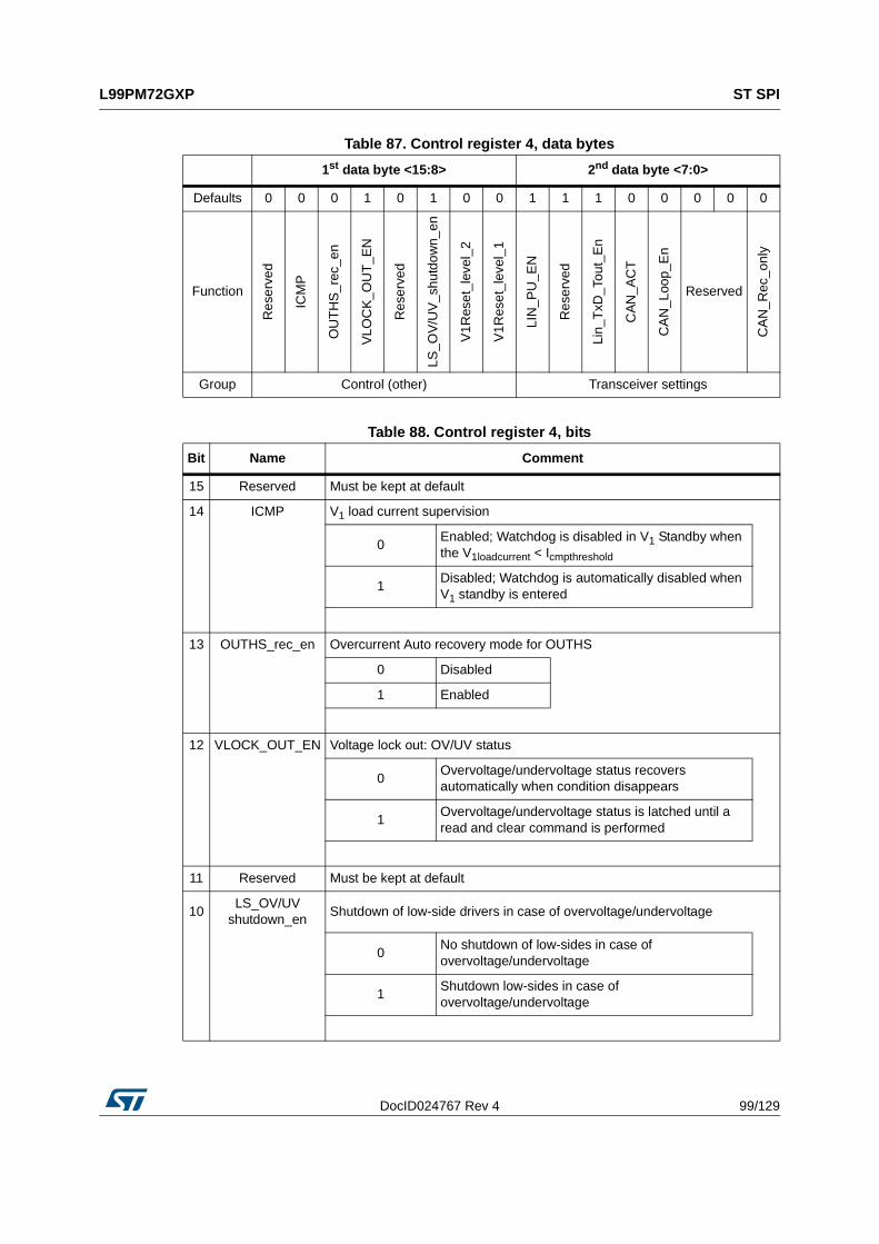
DocID024767 Rev 4 99/129
L99PM72GXP ST SPI
128
Table 87. Control register 4, data bytes
1st data byte <15:8> 2nd data byte <7:0>
Defaults 0 0 0 1 0 1 0 0 1 1 1 0 0 0 0 0
Function
Res
erve
d
ICM
P
OU
TH
S_r
ec_e
n
VLO
CK
_OU
T_E
N
Res
erve
d
LS_O
V/U
V_s
hutd
own_
en
V1R
eset
_lev
el_2
V1R
eset
_lev
el_1
LIN
_PU
_EN
Res
erve
d
Lin_
TxD
_Tou
t_E
n
CA
N_A
CT
CA
N_L
oop_
En
Reserved
CA
N_R
ec_o
nly
Group Control (other) Transceiver settings
Table 88. Control register 4, bits
Bit Name Comment
15 Reserved Must be kept at default
14 ICMP V1 load current supervision
0Enabled; Watchdog is disabled in V1 Standby when the V1loadcurrent < Icmpthreshold
1Disabled; Watchdog is automatically disabled when V1 standby is entered
13 OUTHS_rec_en Overcurrent Auto recovery mode for OUTHS
0 Disabled
1 Enabled
12 VLOCK_OUT_EN Voltage lock out: OV/UV status
0Overvoltage/undervoltage status recovers automatically when condition disappears
1Overvoltage/undervoltage status is latched until a read and clear command is performed
11 Reserved Must be kept at default
10LS_OV/UV
shutdown_enShutdown of low-side drivers in case of overvoltage/undervoltage
0No shutdown of low-sides in case of overvoltage/undervoltage
1Shutdown low-sides in case of overvoltage/undervoltage

ST SPI L99PM72GXP
100/129 DocID024767 Rev 4
9 V1Reset_level_1 Select reset level
8 V1Reset_level_2
V1Reset_level_2
V1Reset_level_1 V1 reset level
0 0 4.6 V
0 1 4.35 V
1 0 4.1 V
1 1 3.8 V
7 LIN_PU_EN Enable internal LIN pull up
0 No LIN master pull-up
1 LIN master pull-up
6 Reserved Must be kept at default
5 Lin_TxD_Tout_En Enable / disable monitoring via TxD
0 No TxD monitoring
1TxD monitoring; LIN transmitter is switched off if TXDL is dominant for t > 12 ms
4 CAN_ACT Activate CAN transceiver
Controls the CAN transceiver mode transition between 'CAN Trx Standby' Mode and 'Trx Normal' mode.The bit CAN_ACT is automatically reset to '0' when the device enters V1_standby Mode or VBat_standby Mode.
0 CAN Trx Standby Mode
1 Trx Normal Mode
See Section 2.9.1 for details.
3 CAN_Loop_En Enable looping of CANTX to CANRXD
0 No looping
1 TXDC is looped to RXDC
2 Reserved Must be kept at default
1 Reserved Must be kept at default
Table 88. Control register 4, bits (continued)
Bit Name Comment

DocID024767 Rev 4 101/129
L99PM72GXP ST SPI
128
6.2.7 Control Register 5
0 CAN_Rec_only Enable CAN receive only mode
0 CAN in transceiver modeActive mode
1 CAN in receive only mode
Table 88. Control register 4, bits (continued)
Bit Name Comment
Table 89. Control register 5: command and data bytes
Command byte 1st data byte 2nd data byte
Read/write Address
x x 0 0 0 1 0 1 Data, 8bit Data, 8 bit
Table 90. Control register 5, data bytes
1st data byte <15:8> 2nd data byte <7:0>
Defaults 0 1 1 1 1 1 1 1 0 0 0 0 0 0 0 0
Function
Res
erve
d
PW
M2_
OF
F_D
C_6
PW
M2_
OF
F_D
C_5
PW
M2_
OF
F_D
C_4
PW
M2_
OF
F_D
C_3
PW
M2_
OF
F_D
C_2
PW
M2_
OF
F_D
C_1
PW
M2_
OF
F_D
C_0
PW
M_F
req
PW
M1_
ON
_DC
_6
PW
M1_
ON
_DC
_5
PW
M1_
ON
_DC
_4
PW
M1_
ON
_DC
_3
PW
M1_
ON
_DC
_2
PW
M1_
ON
_DC
_1
PW
M1_
ON
_DC
_0
Group PWM2 setting PWM1 setting

ST SPI L99PM72GXP
102/129 DocID024767 Rev 4
Table 91. Control register 5, bits
Bit Name Comment
15 Reserved Must be kept at default
14PWM2_
OFF_DC_6PWM2 duty cycle
13PWM2_
OFF_DC_5
PWM2OFF_DC_6
PWM2OFF_DC_5
PWM2OFF_DC_4
PWM2OFF_DC_3
PWM2OFF_DC_2
PWM2OFF_DC_1
PWM2OFF_DC_0
PWM2 duty cycle
12PWM2_
OFF_DC_41 1 1 1 1 1 1 0%, HS OFF
11PWM2_
OFF_DC_31 1 1 1 1 1 0 200/128 %
10PWM2_
OFF_DC_21 1 1 1 1 1 1 300/128 %
9PWM2_
OFF_DC_1...
8 PWM2_OFF_DC_0
0 0 0 0 0 1 0 12600/128 %
0 0 0 0 0 0 1 12700/128 %
0 0 0 0 0 0 0 100% HS ON
7 PWM_FREQ Select PWM frequency
0 128 Hz
1 256 Hz
6PWM1_
ON_DC_6PWM1 duty cycle
5PWM1_
ON_DC_5
PWM1ON_DC_6
PWM1ON_DC_5
PWM1ON_DC_4
PWM1ON_DC_3
PWM1ON_DC_2
PWM1ON_DC_1
PWM1ON_DC_0
PWM1 duty cycle
4PWM1_
ON_DC_41 1 1 1 1 1 1 100%, HS ON
3PWM1_
ON_DC_31 1 1 1 1 1 0 12600/128 %
2PWM1_
ON_DC_21 1 1 1 1 1 1 12500/128 %
1PWM1_
ON_DC_1...
0 PWM1_ON_DC_0
0 0 0 0 0 1 0 200/128 %
0 0 0 0 0 0 1 100/128 %
0 0 0 0 0 0 0 0% HS OFF

DocID024767 Rev 4 103/129
L99PM72GXP ST SPI
128
6.2.8 Control Register 6
Table 92. Control register 6: command and data bytes
Command byte 1st data byte 2nd data byte
Read/write Address
x x 0 0 0 1 1 0 Data, 8bit Data, 8 bit
Table 93. Control register 6, data bytes
1st data byte <15:8> 2nd data byte <7:0>
Defaults 0 1 1 1 1 1 1 1 0 0 0 0 0 0 0 0
Function
Res
erve
d
PW
M4_
OF
F_D
C_6
PW
M4_
OF
F_D
C_5
PW
M4_
OF
F_D
C_4
PW
M4_
OF
F_D
C_3
PW
M4_
OF
F_D
C_2
PW
M4_
OF
F_D
C_1
PW
M4_
OF
F_D
C_0
Res
erve
d
PW
M3_
ON
_DC
_6
PW
M3_
ON
_DC
_5
PW
M3_
ON
_DC
_4
PW
M3_
ON
_DC
_3
PW
M3_
ON
_DC
_2
PW
M3_
ON
_DC
_1
PW
M3_
ON
_DC
_0
Group PWM4 setting PWM3 setting
Table 94. Control register 6, bits
Bit Name Comment
15 Reserved Must be kept at default
14PWM4_
OFF_DC_6PWM4 duty cycle
13PWM4_
OFF_DC_5
PWM4OFF_DC_6
PWM4OFF_DC_5
PWM4OFF_DC_4
PWM4OFF_DC_3
PWM4OFF_DC_2
PWM4OFF_DC_1
PWM4OFF_DC_0
PWM4 duty cycle
12PWM4_
OFF_DC_41 1 1 1 1 1 1 0%, HS OFF
11PWM4_
OFF_DC_31 1 1 1 1 1 0 200/128 %
10PWM4_
OFF_DC_21 1 1 1 1 1 1 300/128 %
9PWM4_
OFF_DC_1...
8 PWM4_OFF_DC_0
0 0 0 0 0 1 0 12600/128 %
0 0 0 0 0 0 1 12700/128 %
0 0 0 0 0 0 0 100% HS ON
7 Reserved Must be kept at default

ST SPI L99PM72GXP
104/129 DocID024767 Rev 4
6PWM3_
ON_DC_6PWM3 duty cycle
5PWM3_
ON_DC_5
PWM3ON_DC_6
PWM3ON_DC_5
PWM3ON_DC_4
PWM3ON_DC_3
PWM3ON_DC_2
PWM3ON_DC_1
PWM3ON_DC_0
PWM3 duty cycle
4PWM3_
ON_DC_41 1 1 1 1 1 1 100%, HS ON
3PWM3_
ON_DC_31 1 1 1 1 1 0 12600/128 %
2PWM3_
ON_DC_21 1 1 1 1 1 1 12500/128 %
1PWM3_
ON_DC_1...
0 PWM3_ON_DC_0
0 0 0 0 0 1 0 200/128 %
0 0 0 0 0 0 1 100/128 %
0 0 0 0 0 0 0 0% HS OFF
Table 94. Control register 6, bits (continued)
Bit Name Comment

DocID024767 Rev 4 105/129
L99PM72GXP ST SPI
128
6.2.9 Control Register 7
Table 95. Control register 7: command and data bytes
Command byte 1st data byte 2nd data byte
Read/write Address
x x 0 0 0 1 1 1 Data, 8bit Data, 8 bit
Table 96. Control register 7, data bytes
1st data byte <15:8> 2nd data byte <7:0>
Defaults 0 0 0 0 0 0 0 0 0 0 0 0 0 0 0 0
Function
EX
T_I
D_1
5
EX
T_I
D_1
4
EX
T_I
D_1
3
EX
T_I
D_1
2
EX
T_I
D_1
1
EX
T_I
D_1
0
EX
T_I
D_9
EX
T_I
D_8
EX
T_I
D_7
EX
T_I
D_6
EX
T_I
D_5
EX
T_I
D_4
EX
T_I
D_3
EX
T_I
D_2
EX
T_I
D_1
EX
T_I
D_0
Group Selective Wakeup Settings
Table 97. Control register 7, bits
Bit Name Comment
15 EXT_ID_15
Extended CAN IdentifierDefinition of which Extended CAN Identifier will wake up
To run matching on Extended CAN Identifier also CAN IDE (Control Register 9 must be set)
14 EXT_ID_14
13 EXT_ID_13
12 EXT_ID_12
11 EXT_ID_11
10 EXT_ID_10
9 EXT_ID_9
8 EXT_ID_8
7 EXT_ID_7
6 EXT_ID_6
5 EXT_ID_5
4 EXT_ID_4
3 EXT_ID_3
2 EXT_ID_2
1 EXT_ID_1
0 EXT_ID_0

ST SPI L99PM72GXP
106/129 DocID024767 Rev 4
6.2.10 Control Register 8
Table 98. Control register 8: command and data bytes
Command byte 1st data byte 2nd data byte
Read/write Address
x x 0 0 1 0 0 0 Data, 8 bit Data, 8 bit
Table 99. Control register 8, data bytes
1st data byte <15:8> 2nd data byte <7:0>
Defaults 0 0 0 0 0 0 0 0 0 0 0 0 0 0 0 0
Function Reserved
ID_1
0
ID_9
ID_8
ID_7
ID_6
ID_5
ID_4
ID_3
ID_2
ID_1
ID_0
EX
T_I
D_1
7
EX
T_I
D_1
6
Group Selective Wakeup Settings
Table 100. Control register 8, bits
Bit Name Comment
15 Reserved
Must be kept at default14 Reserved
13 Reserved
12 ID_10
Standard CAN IdentifierDefinition of which Standard CAN Identifier will wake up
11 ID_9
10 ID_8
9 ID_7
8 ID_6
7 ID_5
6 ID_4
5 ID_3
4 ID_2
3 ID_1
2 ID_0
1 EXT_ID_17 Extended CAN IdentifierDefinition of which Extended CAN Identifier will wake up
To run matching on Extended CAN Identifier also CAN IDE (Control Register 9 must be set)
0 EXT_ID_16
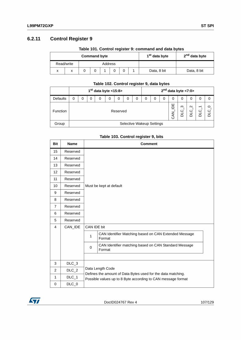
DocID024767 Rev 4 107/129
L99PM72GXP ST SPI
128
6.2.11 Control Register 9
Table 101. Control register 9: command and data bytes
Command byte 1st data byte 2nd data byte
Read/write Address
x x 0 0 1 0 0 1 Data, 8 bit Data, 8 bit
Table 102. Control register 9, data bytes
1st data byte <15:8> 2nd data byte <7:0>
Defaults 0 0 0 0 0 0 0 0 0 0 0 0 0 0 0 0
Function Reserved
CA
N_I
DE
DLC
_3
DLC
_2
DLC
_1
DLC
_0
Group Selective Wakeup Settings
Table 103. Control register 9, bits
Bit Name Comment
15 Reserved
Must be kept at default
14 Reserved
13 Reserved
12 Reserved
11 Reserved
10 Reserved
9 Reserved
8 Reserved
7 Reserved
6 Reserved
5 Reserved
4 CAN_IDE CAN IDE bit
1CAN Identifier Matching based on CAN Extended Message Format
0CAN Identifier matching based on CAN Standard Message Format
3 DLC_3Data Length CodeDefines the amount of Data Bytes used for the data matching.Possible values up to 8 Byte according to CAN message format
2 DLC_2
1 DLC_1
0 DLC_0

ST SPI L99PM72GXP
108/129 DocID024767 Rev 4
6.2.12 Control Register 10
6.2.13 Control Register 11
Table 104. Control register 10: command and data bytes
Command byte 1st data byte 2nd data byte
Read/write Address
x x 0 0 1 0 1 0 Data, 8 bit Data, 8 bit
Table 105. Control register 10, data bytes
1st data byte <15:8> 2nd data byte <7:0>
Defaults 0 0 0 0 0 0 0 0 0 0 0 0 0 0 0 0
Function Data Byte2 Data Byte1
Group Selective Wakeup Settings
Table 106. Control register 10, bits
Bit Name Comment
15 - 8 Data Byte2 Data field for data matching
7 - 0 Data Byte1 Data field for data matching
Table 107. Control register 11: command and data bytes
Command byte 1st data byte 2nd data byte
Read/write Address
x x 0 0 1 0 1 1 Data, 8 bit Data, 8 bit
Table 108. Control register 11, data bytes
1st data byte <15:8> 2nd data byte <7:0>
Defaults 0 0 0 0 0 0 0 0 0 0 0 0 0 0 0 0
Function Data Byte4 Data Byte3
Group Selective Wakeup Settings
Table 109. Control register 11, bits
Bit Name Comment
15 - 8 Data Byte4 Data field for data matching
7 - 0 Data Byte3 Data field for data matching

DocID024767 Rev 4 109/129
L99PM72GXP ST SPI
128
6.2.14 Control Register 12
6.2.15 Control Register 13
Table 110. Control register 12: command and data bytes
Command byte 1st data byte 2nd data byte
Read/write Address
x x 0 0 1 1 0 0 Data, 8 bit Data, 8 bit
Table 111. Control register 12, data bytes
1st data byte <15:8> 2nd data byte <7:0>
Defaults 0 0 0 0 0 0 0 0 0 0 0 0 0 0 0 0
Function Data Byte6 Data Byte5
Group Selective Wakeup Settings
Table 112. Control register 12, bits
Bit Name Comment
15 - 8 Data Byte6 Data field for data matching
7 - 0 Data Byte5 Data field for data matching
Table 113. Control register 13: command and data bytes
Command byte 1st data byte 2nd data byte
Read/write Address
x x 0 0 1 1 0 1 Data, 8 bit Data, 8 bit
Table 114. Control register 13, data bytes
1st data byte <15:8> 2nd data byte <7:0>
Defaults 0 0 0 0 0 0 0 0 0 0 0 0 0 0 0 0
Function Data Byte8 Data Byte7
Group Selective Wakeup Settings
Table 115. Control register 13, bits
Bit Name Comment
15 - 8 Data Byte8 Data field for data matching
7 - 0 Data Byte7 Data field for data matching
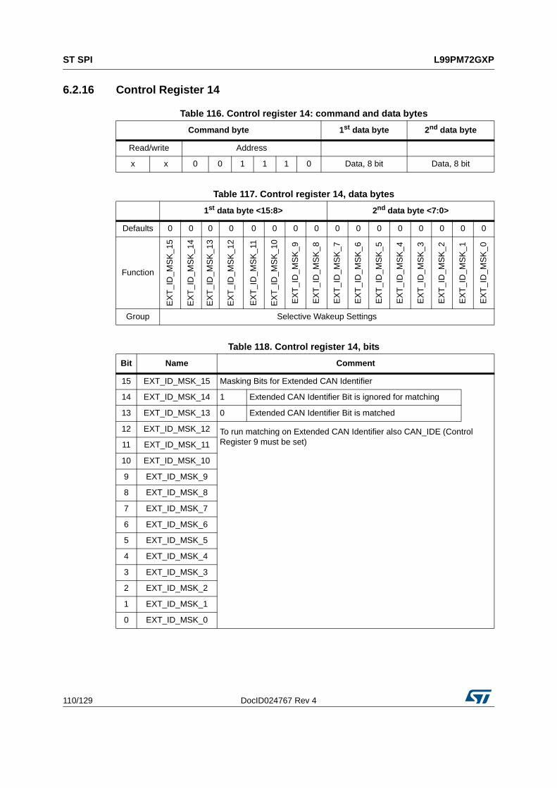
ST SPI L99PM72GXP
110/129 DocID024767 Rev 4
6.2.16 Control Register 14
Table 116. Control register 14: command and data bytes
Command byte 1st data byte 2nd data byte
Read/write Address
x x 0 0 1 1 1 0 Data, 8 bit Data, 8 bit
Table 117. Control register 14, data bytes
1st data byte <15:8> 2nd data byte <7:0>
Defaults 0 0 0 0 0 0 0 0 0 0 0 0 0 0 0 0
Function
EX
T_I
D_M
SK
_15
EX
T_I
D_M
SK
_14
EX
T_I
D_M
SK
_13
EX
T_I
D_M
SK
_12
EX
T_I
D_M
SK
_11
EX
T_I
D_M
SK
_10
EX
T_I
D_M
SK
_9
EX
T_I
D_M
SK
_8
EX
T_I
D_M
SK
_7
EX
T_I
D_M
SK
_6
EX
T_I
D_M
SK
_5
EX
T_I
D_M
SK
_4
EX
T_I
D_M
SK
_3
EX
T_I
D_M
SK
_2
EX
T_I
D_M
SK
_1
EX
T_I
D_M
SK
_0
Group Selective Wakeup Settings
Table 118. Control register 14, bits
Bit Name Comment
15 EXT_ID_MSK_15 Masking Bits for Extended CAN Identifier
14 EXT_ID_MSK_14 1 Extended CAN Identifier Bit is ignored for matching
13 EXT_ID_MSK_13 0 Extended CAN Identifier Bit is matched
12 EXT_ID_MSK_12 To run matching on Extended CAN Identifier also CAN_IDE (Control Register 9 must be set)11 EXT_ID_MSK_11
10 EXT_ID_MSK_10
9 EXT_ID_MSK_9
8 EXT_ID_MSK_8
7 EXT_ID_MSK_7
6 EXT_ID_MSK_6
5 EXT_ID_MSK_5
4 EXT_ID_MSK_4
3 EXT_ID_MSK_3
2 EXT_ID_MSK_2
1 EXT_ID_MSK_1
0 EXT_ID_MSK_0

DocID024767 Rev 4 111/129
L99PM72GXP ST SPI
128
6.2.17 Control Register 15
Table 119. Control register 15: command and data bytes
Command byte 1st data byte 2nd data byte
Read/write Address
x x 0 0 1 1 1 1 Data, 8bit Data, 8 bit
Table 120. Control register 15, data bytes
1st data byte <15:8> 2nd data byte <7:0>
Defaults 0 0 0 0 0 0 0 0 0 0 0 0 0 0 0 0
Function Reserved
ID_M
SK
_10
ID_M
SK
_9
ID_M
SK
_8
ID_M
SK
_7
ID_M
SK
_6
ID_M
SK
_5
ID_M
SK
_4
ID_M
SK
_3
ID_M
SK
_2
ID_M
SK
_1
ID_M
SK
_0
EX
T_I
D_M
SK
_17
EX
T_I
D_M
SK
_16
Group Selective Wakeup Settings
Table 121. Control register 15, bits
Bit Name Comment
15 Reserved
Must be kept at default14 Reserved
13 Reserved
12 ID_MSK_10 Masking Bits for Standard CAN Identifier
11 ID_MSK_9 1 Standard CAN Identifier Bit is ignored for matching
10 ID_MSK_8 0 Standard CAN Identifier Bit is matched
9 ID_MSK_7
8 ID_MSK_6
7 ID_MSK_5
6 ID_MSK_4
5 ID_MSK_3
4 ID_MSK_2
3 ID_MSK_1
2 ID_MSK_0
1 EXT_ID_MSK_17 Masking Bits for Extended CAN Identifier
0 EXT_ID_MSK_16 1 Extended CAN Identifier Bit is ignored for matching
0 Extended CAN Identifier Bit is matched
To run matching on Extended CAN Identifier also CAN_IDE (Control Register 9 must be set)
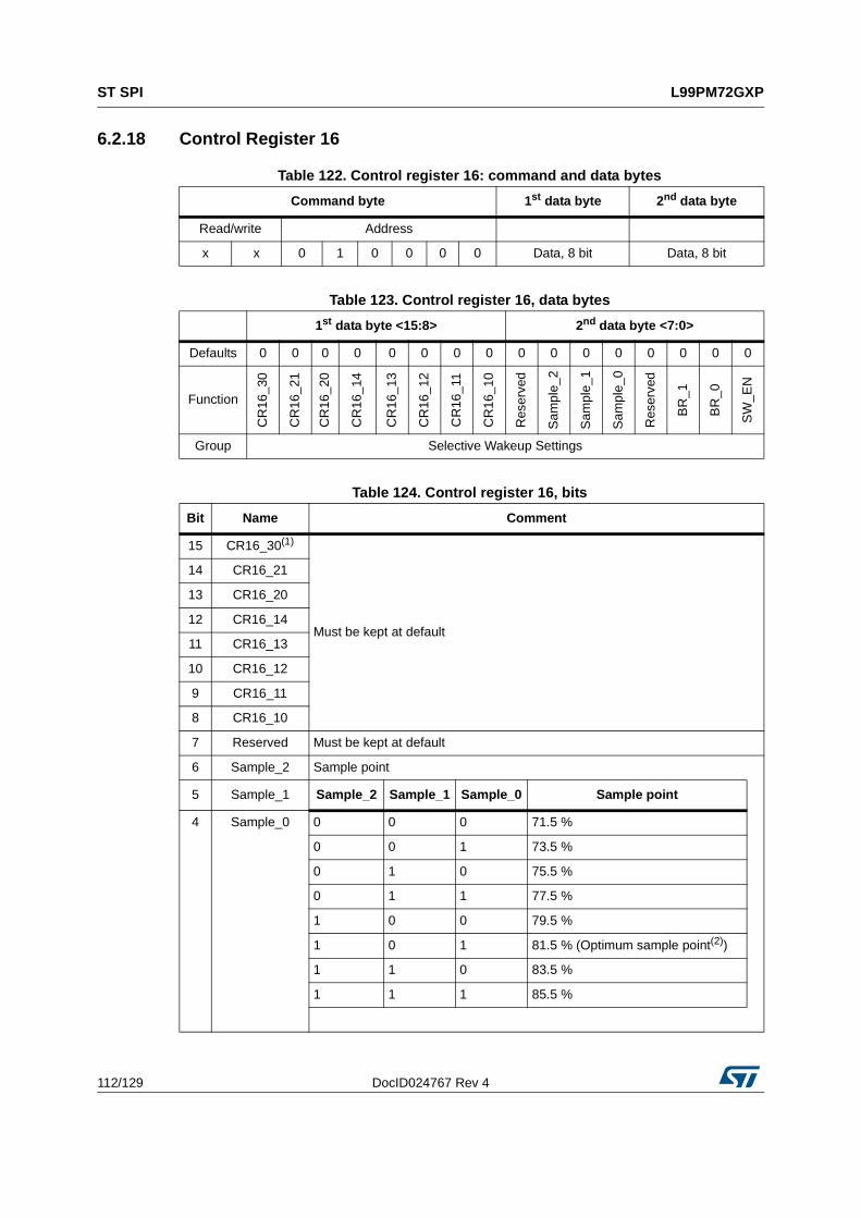
ST SPI L99PM72GXP
112/129 DocID024767 Rev 4
6.2.18 Control Register 16
Table 122. Control register 16: command and data bytes
Command byte 1st data byte 2nd data byte
Read/write Address
x x 0 1 0 0 0 0 Data, 8 bit Data, 8 bit
Table 123. Control register 16, data bytes
1st data byte <15:8> 2nd data byte <7:0>
Defaults 0 0 0 0 0 0 0 0 0 0 0 0 0 0 0 0
Function
CR
16_3
0
CR
16_2
1
CR
16_2
0
CR
16_1
4
CR
16_1
3
CR
16_1
2
CR
16_1
1
CR
16_1
0
Res
erve
d
Sam
ple_
2
Sam
ple_
1
Sam
ple_
0
Res
erve
d
BR
_1
BR
_0
SW
_EN
Group Selective Wakeup Settings
Table 124. Control register 16, bits
Bit Name Comment
15 CR16_30(1)
Must be kept at default
14 CR16_21
13 CR16_20
12 CR16_14
11 CR16_13
10 CR16_12
9 CR16_11
8 CR16_10
7 Reserved Must be kept at default
6 Sample_2 Sample point
5 Sample_1 Sample_2 Sample_1 Sample_0 Sample point
4 Sample_0 0 0 0 71.5 %
0 0 1 73.5 %
0 1 0 75.5 %
0 1 1 77.5 %
1 0 0 79.5 %
1 0 1 81.5 % (Optimum sample point(2))
1 1 0 83.5 %
1 1 1 85.5 %

DocID024767 Rev 4 113/129
L99PM72GXP ST SPI
128
3 Reserved Must be kept at default
2 BR_1 CAN baud rate
1 BR_0 BR_1 BR_0 Baud rate
0 0 500 kbit/s
0 1 250 kbit/s
1 0 Oscillator stopped (see Oscillator monitoring)
1 1 125 kbit/s
0 SW_EN(3) Selective Wakeup Enable
0 No selective wakeup
1 Selective wakeup enabled
See Section 2.9.2
1. Changing the default configuration of CR16 (bits 1 to 15) is only possible when selective wake is disabled (SW_EN = 0). Setting SW_EN = 0 is always possible. Setting SW_EN = 1 must follow the procedure as described in Section 2.9.2.
2. The sampling point bits [6:4] have to be programmed to “101” (81.5%) before enabling the selective wake-up feature.
3. SW_EN enables CAN WUF independently from the status of CAN_WAKE_EN.
Table 124. Control register 16, bits (continued)
Bit Name Comment

ST SPI L99PM72GXP
114/129 DocID024767 Rev 4
6.2.19 Control Register 34
Table 125. Control register 34: command and data bytes
Command byte 1st data byte 2nd data byte
Read/write Address
x x 1 0 0 0 1 0 Data, 8 bit Data, 8 bit
Table 126. Control register 34, data bytes
1st data byte <15:8> 2nd data byte <7:0>
Defaults 0 0 0 0 0 0 0 0 0 0 0 0 0 0 0 1
Function Reserved
WD
_EN
Group Selective Wakeup Settings
Table 127. Control register 34, bits
Bit Name Comment
15 Reserved
Must be kept at default
14 Reserved
13 Reserved
12 Reserved
11 Reserved
10 Reserved
9 Reserved
8 Reserved
7 Reserved
6 Reserved
5 Reserved
4 Reserved
3 Reserved
2 Reserved
1 Reserved
0 WD_EN Watchdog enabled bit
0 Watchdog disabled
1 Watchdog enabled
Writing to this bit is only possible during CAN Flash Mode (VTxDL > VFlash). See Section 2.2.2: Flash Mode.

DocID024767 Rev 4 115/129
L99PM72GXP ST SPI
128
6.2.20 Control Register 35
Table 128. Control register 35: command and data bytes
Command byte 1st data byte 2nd data byte
Read/write Address
x x 1 0 0 0 1 1 Data, 8 bit Data, 8 bit
Table 129. Control register 35, data bytes
1st data byte <15:8> 2nd data byte <7:0>
Defaults 0 0 0 0 0 0 0 0 0 0 1 1 0 1 1 0
Function Reserved
CR
35_2
5
CR
35_2
4
CR
35_2
3
CR
35_2
2
CR
35_2
1
CR
35_2
0
CR
35_1
0
Group Selective Wakeup Settings
Table 130. Control register 35, bits
Bit Name Comment
15 Reserved
Must be kept at default
14 Reserved
13 Reserved
12 Reserved
11 Reserved
10 Reserved
9 Reserved
8 Reserved
7 Reserved
6 CR35_25
Must be kept at default
5 CR35_24
4 CR35_23
3 CR35_22
2 CR35_21
1 CR35_20
0 CR35_10 Must be kept at default

ST SPI L99PM72GXP
116/129 DocID024767 Rev 4
6.2.21 Overview status register
Table 131. Overview of status register data bytes
1st data byte <15:8> 2nd data byte <7:0>
Status register 1, data <15:0>
Function
OL_
HS
OL_
OU
T4
OL_
OU
T3
OL_
OU
T2
OL_
OU
T1
UV
V2_
fail
V2_
shor
t
OV
OC
_HS
OC
_OU
T4
OC
_OU
T3
OC
_OU
T2
OC
_OU
T1
OC
_RE
L2
OC
_RE
L1
Group Diagnosis 1 Diagnosis 2
Status register 2, data <15:0>
Function
WU
3_st
ate
WU
2_st
ate
WU
1_st
ate
WU
3_w
ake
WU
2_w
ake
WU
1_W
ake
Wak
e_C
AN
Wak
e_LI
N
Wak
e_Ti
mer
_int
LIN
_per
m_d
om
LIN
_TxD
_per
m_d
om
LIN
_per
m_r
ec
CA
N_R
xD_
perm
_rec
CA
N_p
erm
_rec
CA
N_p
erm
_dom
CA
N_T
xD_
perm
_dom
Group Diagnosis 3 Diagnosis 4
Status register 3, data <15:0>
Function
TS
D1
TW
Dev
ice_
stat
e
Dev
ice_
stat
e
V1_
fail
V1_
rest
art
V1_
rest
art
V1_
rest
art
WD
_fai
l
WD
_fai
l
WD
_fai
l
WD
_fai
l
For
ced_
slee
p_W
D
For
ced_
slee
p_T
SD
2_S
HT
V1
WD
_tim
er_s
tate
WD
_tim
er_s
tate
Group Diagnosis 5 Diagnosis 6
Status register 4, data <15:0>
Function
SW
RD
_15
SW
RD
_14
SW
RD
_13
SW
RD
_12
SW
RD
_11
SW
RD
_10
SW
RD
_9
SW
R_D
8
SW
RD
_7
SY
S_E
RR
TX
_SY
NC
CA
N_T
O
WU
P
WU
F
CA
N_s
ilent
FD
_ER
R
Group Diagnosis 7 Diagnosis 8
Status register 5, data <15:0>
Function Reserved
FE
CN
T_4
FE
CN
T_3
FE
CN
T_2
FE
CN
T_1
FE
CN
T_0
OS
C_F
AIL
Reserved Osc_Mon
Group Diagnosis 9 Diagnosis 10

DocID024767 Rev 4 117/129
L99PM72GXP ST SPI
128
6.2.22 Global status register
The Global Error Flag is set once the watchdog failure counter (SR3<7:4>) is unequal to 0 (see also Section 2.5: Fail Safe Mode).
Table 132. Global status register
Bit 7 Bit 6 Bit 5 Bit 4 Bit 3 Bit 2 Bit 1 Bit 0
Hex value
Glo
bal
err
or
flag
(1)
Co
mm
un
icat
ion
erro
r (2
)
NO
T (
chip
res
et
or
com
m e
rro
r)(3
)
TS
D2(4
)
TS
D1
V1
Fai
l
VS F
ail
(OV
/UV
) (5
)
Fai
l saf
e(6)
Active high/low High High Low High High High High High
Default value in Normal Mode - after correct WD trigger or after Read & Clear
on Error Flags0 0 1 0 0 0 0 0 20
Power ON 1 0 0 0 0 0 0 0 80
Power ON weak battery (7) 1 0 0 0 0 0 1 0 82
Communication error 1 1 0 0 0 0 0 0 C0
VS overvoltage or undervoltage 1 0 1 0 0 0 1 0 A2
WD failure 1 0 1 0 0 0 0 1 A1
SPI Error (DI Stuck) 1 0 1 0 0 0 0 1 A1
TSD1 1 0 1 0 1 0 0 0 A8
TSD2 1 0 1 1 1 0 0 1 B9
V1 Fail 1 0 1 0 0 1 0 0 A4
Other Device Failure(8) 1 0 1 0 0 0 0 0 A0
1. The following Status Bits are reported in the Global Error Flag:Global Status Register: Bits 6-0Status Register 1: Bits 10-0Status Register 3: Bits 15, 11, 7-2
2. Communication Error: invalid number of CLOCK cycles during CSN low or failed parity check on standby command.
3. Cleared with CLR command on SR3.
4. Cleared with “READ and CLEAR” on SR3 (-> TSD1)
5. Diagnosis bit only, VS Fail is not a Fail-Safe event; cleared by Read&Clear. Bit is automatically cleared at (VS > VSUV) and (VS < VSOV) if Vlock_out_en = 0
6. Cleared with a valid WD trigger (WD fail) or by clearing the corresponding status register related to failure. It is recommended that the microcontroller does not enter standby mode, if a fail-safe event is indicated in the Global Status Register. The selective wake-up configuration in CR 7 to 15 has to be re-written before sending the standby command.
7. Slow VS ramp-up (VS undervoltage is filtered with 64µs after power-on reset)
8. The Global Error Flag is raised due to a failure condition which is not reported in the Global Status Register. The Failure is reported in the Status Registers 1-5

ST SPI L99PM72GXP
118/129 DocID024767 Rev 4
6.2.23 Status Register 1
Table 133. Status register 1: command and data bytes
Command byte 1st data byte 2nd data byte
Read/write Address Bit <15:8> Bit <7:0>
x x 0 1 0 0 0 1 Data, 8bit Data, 8 bit
Table 134. Status register 1, data bytes
1st data byte <15:8> 2nd data byte <7:0>
Function
OL_
HS
OL_
OU
T4
OL_
OU
T3
OL_
OU
T2
OL_
OU
T1
UV
V2_
fail
V2_
shor
t
OV
OC
_HS
OC
_OU
T4
OC
_OU
T3
OC
_OU
T2
OC
_OU
T1
OC
_RE
L2
OC
_RE
L1
Group Diagnosis 1 Diagnosis 2
Table 135. Status register 1, bits
Bit Name Comment Information storage
15 OL_HS
Open-load event occurred since last read out
Bit is latched until a “read and clear” access
14 OL_OUT4
13 OL_OUT3
12 OL_OUT2
11 OL_OUT1
10 UV
Under voltage event on VS occurred since last read out
VLOCKOUTEN (CR4)
Information storage
0automatically reset when UV condition disappears
1Bit is latched until a “read and clear” access
9 V2_failV2 fail (V2 < 2 V for t> 2 µs) event occurred since last readout
Bit is latched until a “Read and clear” access
8 V2_shortV2 short (V2 < 2 V for t > 4ms during start up) event occurred since last readout
Bit is latched until a “Read and clear” access

DocID024767 Rev 4 119/129
L99PM72GXP ST SPI
128
7 OV
Over voltage event on VS occurred since last read out
VLOCKOUTEN (CR4)
Information storage
0automatically reset when OV condition disappears
1Bit is latched until a “read and clear” access
6 OC_HS
Over current event occurred since last read out
Bit is latched until a “read and clear” access
5 OC_OUT4
4 OC_OUT3
3 OC_OUT2
2 OC_OUT1
1 OC_REL2
0 OC_REL1
Table 135. Status register 1, bits (continued)
Bit Name Comment Information storage

ST SPI L99PM72GXP
120/129 DocID024767 Rev 4
6.2.24 Status Register 2
Table 136. Status register 2: command and data bytes
Command byte 1st data byte 2nd data byte
Read/write Address Bit <15:8> Bit <7:0>
x x 0 1 0 0 1 0 Data, 8bit Data, 8 bit
Table 137. Status register 2, data bytes
1st data byte <15:8> 2nd data byte <7:0>
Function
WU
3_st
ate
WU
2_st
ate
WU
1_st
ate
WU
3_w
ake
WU
2_w
ake
WU
1_w
ake
Wak
e_C
AN
Wak
e_LI
N
Wak
e_Ti
mer
_int
LIN
_per
m_d
om
LIN
_TxD
_per
m_d
om
LIN
_per
m_r
ec
CA
N_R
xD_p
erm
_rec
CA
N_p
erm
_rec
CA
N_p
erm
_dom
CA
N_T
xD_p
erm
_dom
Group Diagnosis 3 Diagnosis 4
Table 138. Status register 2, bits
Bit Name Comment Information storage
15 WU3_state
State of WUx input; “Live bits” not clearable14 WU2_state
13 WU1_state
12 WU3_wake
Shows wake up source (‘1’ = wake-up)Bits are latched until a “Read and clear” access
11 WU2_wake
10 WU1_wake
9 WAKE_CAN(1)
8 WAKE_LIN
7 Wake_TIMER_int

DocID024767 Rev 4 121/129
L99PM72GXP ST SPI
128
6.2.25 Status Register 3
6 LIN_perm_DOM LIN bus is dominant for t > 12 ms
Bits are latched until a “Read and clear” access
5 LIN_TxD_perm_DOMTxDL pin is dominant for t > 12 ms; Transmitter is disabled
4 LIN_perm_RECLIN bus does not follow TxDL within 40 µs; Transmitter is disabled
3 CAN_RxD_perm_recRxDC has not followed TxDC for 4 times; Transmitter is disabled
2 CAN_perm_RECCAN has not followed TxDC for 4 times; Transmitter is disabled
1 CAN_perm_DOM CAN bus is dominant for t > 700 µs
0 CAN_TxD_perm_DOMTxDC pin is dominant for t > 700 µs; Transmitter is disabled
1. The bit is set only if CAN_WU_EN = 1; the bit does not indicate a wake-up by CAN wake-up frame (WUF).
Table 138. Status register 2, bits (continued)
Bit Name Comment Information storage
Table 139. Status register 3: command and data bytes
Command byte 1st data byte 2nd data byte
Read/write Address Bit <15:8> Bit <7:0>
x x 0 1 0 0 1 1 Data, 8bit Data, 8 bit
Table 140. Status register 3, data bytes
1st data byte <15:8> 2nd data byte <7:0>
Function
TS
D1
TW
Dev
ice_
stat
e_1
Dev
ice_
stat
e_0
V1_
fail
V1_
rest
art_
2
V1_
rest
art_
1
V1_
rest
art_
0
WD
_fai
l_3
WD
_fai
l_2
WD
_fai
l_1
WD
_fai
l_0
For
ced_
slee
p_W
D
For
ced_
slee
p_T
SD
2_S
HT
V1
WD
_tim
er_s
tate
_1
WD
_tim
er_s
tate
_0
Group Diagnosis 5 Diagnosis 6
Table 141. Status register 3, bits
Bit Name CommentInformation
storage
15 TSD1Thermal warning / shutdown1 occurred since last readout
Bit is latched until a “read and clear access”14 TW

ST SPI L99PM72GXP
122/129 DocID024767 Rev 4
13
Device_state
State from which the device woke upBit is latched until a “read and clear access” after a “read and clear access”, the device state is updated. After a wake up, device state is:01: V1_standby
or 10: VBat_standby
12 Device state_2 Device state_1
State from which the
device woke up
0 0 Active
0 1 V1_standby
1 0 VBat_standby
1 1 Flash
11 V1_failV1 fail (V1 < 2 V for t > 2 µs) event occurred since last read out
Bit is latched until a “read and clear access”
10 V1_restart_2
Number of TSD2 events which caused a restart of V1 regulator (7 TSD2 events forces the device into VBat_standby)
Bits are not clearable; is cleared automatically if no additional TSD2 event occurs within 1 min.
9 V1_restart_1
8 V1_restart_0
7 WD_fail_3
Number of missing watchdog triggers (15 missing watchdog trigger forces the device into VBat_standby)
Bits are not clearable; is cleared with a proper Watchdog trigger
6 WD_fail_2
5 WD_fail_1
4 WD_fail_0
3 Forced_sleep_WDDevice was forced to VBat_standby mode because of multiple watchdog errors Bits are latched until
a read and clear access2
Forced_sleep_TSD2_SHTV1
Device was forced to VBat_standby or multiple thermal shutdown events or a short on V1 during startup.
1 WD_timer_state_1 Status of watchdog counter of selected watchdog timing
Bits are not clearable
0 WD_timer_state_0
WD_timer_state_1
WD_timer_state_0
Counter
0 0 0 – 33%
0 1 33 – 66%
1 1 66 – 100%
Table 141. Status register 3, bits (continued)
Bit Name CommentInformation
storage

DocID024767 Rev 4 123/129
L99PM72GXP ST SPI
128
6.2.26 Status Register 4
Table 142. Status register 4: command and data bytes
Command byte 1st data byte 2nd data byte
Read/write Address Bit <15:8> Bit <7:0>
x x 0 1 0 1 0 0 Data, 8bit Data, 8 bit
Table 143. Status register 4, data bytes
1st data byte <15:8> 2nd data byte <7:0>
Function
SW
RD
_15
SW
RD
_14
SW
RD
_13
SW
RD
_12
SW
RD
_11
SW
RD
_10
SW
RD
_9
SW
RD
_8
SW
RD
_7
SY
S_E
RR
TX
_ S
YN
C
CA
N_T
O
WU
P
WU
F
CA
N_
sile
nt
FD
_ER
R
Group Diagnosis 5 Diagnosis 6
Table 144. Status register 4, bits
Bit Name Comment Information storage
15 SWRD_15
Status flag for Read operation to Selective Wakeup relevant Registers 0: Read not done1: Read done
See also Section 2.10: Serial Peripheral Interface (ST SPI Standard 3.0)
Automatically cleared by a write
14 SWRD_14
13 SWRD_13
12 SWRD_12
11 SWRD_11
10 SWRD_10
9 SWRD_9
8 SWRD_8
7 SWRD_7
6 SYS_ERR
This bit is a logical OR combination of
NOT(SWRD_x) OR OSC_Fail OR FD_ERRThe selective wake feature cannot be enabled (SW_EN = 1) if SYS_ERR = 1In case of a SYS_ERR the selective wake-up feature is disabled (SW_EN = 0)
Live bit be updated while the change of SWRD_x, OSC_Fail and FD_ERR.
If SWRD_x are all 1, OSC_Fail is 0 and FD_ERR is 0, this bit is 0, otherwise this bit is 1.
5 TX_SYNC
Status flag for Synchronous Reference oscillator of the Transceiver. Indicates that the last received frame was decoded correctly0: Not synchron1: Synchron
Live bit updated after each sent CAN frame

ST SPI L99PM72GXP
124/129 DocID024767 Rev 4
4 CAN_TO
CAN timeout, bit is set if there is no communication on the bus for longer than tsilence
Vbat_standby Mode: CAN_TO indicates that there was a transition from PN_TRX_selective_sleep to TRX_SLEEPDuring TRX_STBY Mode (CAN_ACT = 0, Active Mode and V1_standby Mode(1)) this bit indicates a CAN communication timeout. An interrupt on RxDC/NINT is generated in this case.
Bit is latched until a read and clear access
3 WUP Wake up flag for Remote Wake up patternBit is latched until a read and clear access
2 WUF Wake up flag for Remote Wake up FrameBit is latched until a read and clear access
1 CAN_Silent
Online monitoring bit to see if there is silence on the bus for longer than tsilence.This flag shows the actual status of the CAN bus (activity/silence). A microcontroller in Stop Mode may check this flag periodically
Auto cleared and set
0 FD_ERR
Frame Detect Error.
This bit is set at overflow of the Frame Error Counter (FECNT) in SR5
In case of a Frame Detect Error, the device will wake up from PN_Trx_selective_sleep
Bit is latched until a read and clear access
1. It is recommended to clear the bit CAN_TO prior to transition into V1_standby mode.
Table 144. Status register 4, bits (continued)
Bit Name Comment Information storage

DocID024767 Rev 4 125/129
L99PM72GXP ST SPI
128
6.2.27 Status Register 5
Table 145. Status register 5: command and data bytes
Command byte 1st data byte 2nd data byte
Read/write Address Bit <15:8> Bit <7:0>
x x 0 1 0 1 0 1 Data, 8bit Data, 8 bit
Table 146. Status register 5, data bytes
1st data byte <15:8> 2nd data byte <7:0>
Function Reserved
FE
CN
T_4
FE
CN
T_3
FE
CN
T_2
FE
CN
T_1
FE
CN
T_0
OS
C_F
AIL
Reserved
Osc
_mon
Osc
_mon
Osc
_mon
Osc
_mon
Osc
_mon
Group Diagnosis 5 Diagnosis 6
Table 147. Status register 5, bits
Bit Name Comment Information storage
15 Reserved
Must be kept at default14 Reserved
13 Reserved
12 FECNT_4 Frame Detect Error CounterThis counter is increased by 1 in case a frame was not received/decoded correctly (CRC error, stuff-bit error, form error).
The counter is decreased by 1 with every frame which is decoded correctly
If FECNT = 31, the next erroneous frame will wake-up the device, set FDERR = 1 and reset FECNTx = 0
Live bit updated after each sent CAN frame
11 FECNT_3
10 FECNT_2
9 FECNT_1
8 FECNT_0
7 OSC_FAIL OSC Failure Flag (used device internally)Bit is latched until a read and clear access
6 ReservedMust be kept at default
5 Reserved
4 - 0 Osc_mon Monitoring of internal oscillator (used internally)Live bit updated after each sent CAN frame

Package information L99PM72GXP
126/129 DocID024767 Rev 4
7 Package information
7.1 ECOPACK®
In order to meet environmental requirements, ST offers these devices in different grades of ECOPACK® packages, depending on their level of environmental compliance. ECOPACK® specifications, grade definitions and product status are available at: www.st.com. ECOPACK® is an ST trademark.
7.2 PowerSSO-36 mechanical data
Figure 44. PowerSSO-36 package dimensions
AG00066V1
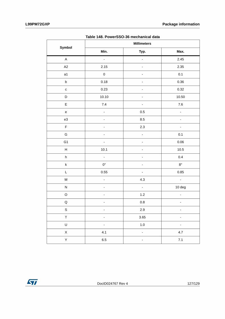
DocID024767 Rev 4 127/129
L99PM72GXP Package information
128
Table 148. PowerSSO-36 mechanical data
SymbolMillimeters
Min. Typ. Max.
A - - 2.45
A2 2.15 - 2.35
a1 0 - 0.1
b 0.18 - 0.36
c 0.23 - 0.32
D 10.10 - 10.50
E 7.4 - 7.6
e - 0.5 -
e3 - 8.5 -
F - 2.3 -
G - - 0.1
G1 - - 0.06
H 10.1 - 10.5
h - - 0.4
k 0° - 8°
L 0.55 - 0.85
M - 4.3 -
N - - 10 deg
O - 1.2 -
Q - 0.8 -
S - 2.9 -
T - 3.65 -
U - 1.0 -
X 4.1 - 4.7
Y 6.5 - 7.1

Revision history L99PM72GXP
128/129 DocID024767 Rev 4
8 Revision history
Table 149. Document revision history
Date Revision Changes
10-Jun-2013 1 Initial release.
19-Sep-2013 2 Updated Disclaimer.
03-Mar-2014 3
Updated Section 2.2.5: Interrupt
Added Section : Oscillator monitoringUpdated Section 2.9.4: Wake up by CANTable 14: Supply and supply monitoring
– Vhyst_UV: updated valuesTable 28: CAN transmitter and receiver: pins CANH and CANL:– VCANHdom, VCANLdom, VDIFF,domOUT: updated test condition
– VCM: updated test condition and added note– VTHdom, VTHdomLP, VTHrec, VTHrecLP: added noteTable 29: CAN transceiver timing:
– tTXpd,hl, tTXpd,hl: updated test conditionTable 91: Control register 5, bits:– PWM2 duty cycle, PWM1 duty cycle: updated values
Table 94: Control register 6, bits:– PWM4 duty cycle, PWM3 duty cycle: updated valuesTable 124: Control register 16, bits:
– SW_EN: added note– BR_0: updated commentTable 138: Status register 2, bits:
– WAKE_CAN: added noteTable 144: Status register 4, bits:– Removed note
24-Apr-2014 4 Updated Section 2.2.2: Flash Mode

DocID024767 Rev 4 129/129
L99PM72GXP
129
Please Read Carefully:
Information in this document is provided solely in connection with ST products. STMicroelectronics NV and its subsidiaries (“ST”) reserve theright to make changes, corrections, modifications or improvements, to this document, and the products and services described herein at anytime, without notice.
All ST products are sold pursuant to ST’s terms and conditions of sale.
Purchasers are solely responsible for the choice, selection and use of the ST products and services described herein, and ST assumes noliability whatsoever relating to the choice, selection or use of the ST products and services described herein.
No license, express or implied, by estoppel or otherwise, to any intellectual property rights is granted under this document. If any part of thisdocument refers to any third party products or services it shall not be deemed a license grant by ST for the use of such third party productsor services, or any intellectual property contained therein or considered as a warranty covering the use in any manner whatsoever of suchthird party products or services or any intellectual property contained therein.
UNLESS OTHERWISE SET FORTH IN ST’S TERMS AND CONDITIONS OF SALE ST DISCLAIMS ANY EXPRESS OR IMPLIEDWARRANTY WITH RESPECT TO THE USE AND/OR SALE OF ST PRODUCTS INCLUDING WITHOUT LIMITATION IMPLIEDWARRANTIES OF MERCHANTABILITY, FITNESS FOR A PARTICULAR PURPOSE (AND THEIR EQUIVALENTS UNDER THE LAWSOF ANY JURISDICTION), OR INFRINGEMENT OF ANY PATENT, COPYRIGHT OR OTHER INTELLECTUAL PROPERTY RIGHT.
ST PRODUCTS ARE NOT DESIGNED OR AUTHORIZED FOR USE IN: (A) SAFETY CRITICAL APPLICATIONS SUCH AS LIFESUPPORTING, ACTIVE IMPLANTED DEVICES OR SYSTEMS WITH PRODUCT FUNCTIONAL SAFETY REQUIREMENTS; (B)AERONAUTIC APPLICATIONS; (C) AUTOMOTIVE APPLICATIONS OR ENVIRONMENTS, AND/OR (D) AEROSPACE APPLICATIONSOR ENVIRONMENTS. WHERE ST PRODUCTS ARE NOT DESIGNED FOR SUCH USE, THE PURCHASER SHALL USE PRODUCTS ATPURCHASER’S SOLE RISK, EVEN IF ST HAS BEEN INFORMED IN WRITING OF SUCH USAGE, UNLESS A PRODUCT ISEXPRESSLY DESIGNATED BY ST AS BEING INTENDED FOR “AUTOMOTIVE, AUTOMOTIVE SAFETY OR MEDICAL” INDUSTRYDOMAINS ACCORDING TO ST PRODUCT DESIGN SPECIFICATIONS. PRODUCTS FORMALLY ESCC, QML OR JAN QUALIFIED AREDEEMED SUITABLE FOR USE IN AEROSPACE BY THE CORRESPONDING GOVERNMENTAL AGENCY.
Resale of ST products with provisions different from the statements and/or technical features set forth in this document shall immediately voidany warranty granted by ST for the ST product or service described herein and shall not create or extend in any manner whatsoever, anyliability of ST.
ST and the ST logo are trademarks or registered trademarks of ST in various countries.Information in this document supersedes and replaces all information previously supplied.
The ST logo is a registered trademark of STMicroelectronics. All other names are the property of their respective owners.
© 2014 STMicroelectronics - All rights reserved
STMicroelectronics group of companies
Australia - Belgium - Brazil - Canada - China - Czech Republic - Finland - France - Germany - Hong Kong - India - Israel - Italy - Japan - Malaysia - Malta - Morocco - Philippines - Singapore - Spain - Sweden - Switzerland - United Kingdom - United States of America
www.st.com