ADVANCED MOBILITY MODELS FOR DESIGN AND … · advanced mobility models for design and simulation...
170
ADVANCED MOBILITY MODELS FOR DESIGN AND SIMULATION OF DEEP SUBMICROMETER MOSFETS A DISSERTATION SUBMITTED TO THE DEPARTMENT OF ELECTRICAL ENGINEERING AND THE COMMITTEE ON GRADUATE STUDIES OF STANFORD UNIVERSITY IN PARTIAL FULFILLMENT OF THE REQUIREMENTS FOR THE DEGREE OF DOCTOR OF PHILOSOPHY By Syed Aon Mujtaba December 1995
Transcript of ADVANCED MOBILITY MODELS FOR DESIGN AND … · advanced mobility models for design and simulation...

ADVANCED MOBILITY MODELS FOR
DESIGN AND SIMULATION
OF DEEP SUBMICROMETER MOSFETS
A DISSERTATION
SUBMITTED TO THE DEPARTMENT OF ELECTRICAL ENGINEERING
AND THE COMMITTEE ON GRADUATE STUDIES
OF STANFORD UNIVERSITY
IN PARTIAL FULFILLMENT OF THE REQUIREMENTS
FOR THE DEGREE OF
DOCTOR OF PHILOSOPHY
By
Syed Aon Mujtaba
December 1995

ii
© Copyright by Syed Aon Mujtaba 1995
All Rights Reserved

iii
I certify that I have read this dissertation and that in my opinion it is fully adequate,
in scope and quality, as a dissertation for the degree of the Doctor of Philosophy.
Robert W. Dutton (Principal Advisor)
I certify that I have read this dissertation and that in my opinion it is fully adequate,
in scope and quality, as a dissertation for the degree of the Doctor of Philosophy.
James D. Plummer (Associate Advisor)
I certify that I have read this dissertation and that in my opinion it is fully adequate,
in scope and quality, as a dissertation for the degree of the Doctor of Philosophy.
Teresa H.-Y. Meng
Approved for the University Committee on Graduate Studies:

iv
Abstract
Carrier mobility is one of the most important parameters affecting the I-V
characteristics of MOSFETs. Hence, accurate mobility models that account for all the
important scattering mechanisms are an essential requirement for predictive MOS device
simulation. This dissertation focuses on issues related to mobility modeling in MOSFETs
as they scale to deep submicron dimensions. A new physically-based mobility model for
two dimensional (2D) device simulation is presented that accurately models MOSFETs
for all channel lengths down to 0.25µm. Enhanced physical features of the new model
include terms for 2D Coulombic scattering and 2D accumulation-layer mobility.
As MOSFETs scale to shorter channel lengths, channel doping levels increase in
order to suppress undesirable short-channel effects such as punchthrough and drain-
induced barrier lowering (DIBL). One direct consequence of increased doping is enhanced
impurity scattering, the importance of which in scaled MOSFETs is established by
demonstrating its impact on critical design parameters such as threshold voltage and
off-state leakage current. An accurate model for impurity scattering has been developed
that, for the first time, properly accounts for 2D confinement and quantum mechanical
effects in the inversion layer. A systematic methodology for extracting Coulombic
mobility from I-V data is also presented. Based on this scheme, it is shown that in regimes
where three dimensional (3D) models grossly over-predict mobility, the new 2D model
demonstrates its broad applicability by accurately reproducing experimental results over a
wide range of channel dopings, substrate biases, and electron concentrations.
Traditionally, channel resistance has been the dominant factor limiting current
transport in MOSFETs. However, in deep submicron MOSFETs with lightly-doped drain
(LDD) structures, channel resistance has become comparable to the parasitic series
resistance, a major component of which comes from the accumulation layer in the LDD
region. A unified mobility model is presented that is applicable in both inversion and
accumulation layers. A systematic methodology is presented for the calibration and

v
validation of the new model with experimental data. Broad applicability of the new model
is established with excellent agreement over a wide range of operating conditions
(subthreshold, linear, and saturation) for gate lengths ranging from 20.0µm down to
0.25µm.

vi
Acknowledgments
A great number of wonderful people have made my Stanford career a very
rewarding and memorable experience.
First and foremost, I would like to express my sincerest gratitude to my advisor and
mentor, Professor Robert W. Dutton for his guidance and support throughout my years at
Stanford. In ways more than one, he has made me realize my fullest potential, and
encouraged me to attain the highest level of professionalism. I would especially like to
thank him for giving me the freedom to pursue my research interests.
I would like to thank Professors James D. Plummer and Teresa H.-Y. Meng for their
expeditious reading of my thesis and for serving on my oral examination committee. I
would also like to thank Professor Bruce A. Wooley for serving on my oral examinations
committee.
I have greatly benefited from the interaction with people in the industry. I am
grateful to Dr. Don Scharfetter of Intel Corporation for mentoring me in my early years of
graduate study. I would like to thank Dr. Shin-ichi Takagi and Mr. Junji Koga of Toshiba
Corporation for their collaboration on the work on Coulombic scattering. I would like to
thank Dr. Yuan Taur of IBM Research for his fruitful and insightful discussions on
mobility modeling. I would like to thank Dr. John Faricelli of DEC for implementing my
mobility model in MINIMOS.
The financial support of Semiconductor Research Corporation is gratefully
acknowledged.
My most rewarding experience was the summer I spent at AT&T Bell Laboratories
in Murray Hill, NJ. I would especially like to thank Drs. Ran Yan, Mark Pinto and Don
Monroe of AT&T Bell Labs for giving me the opportunity to work with them on a variety
of interesting and stimulating topics. I would like to thank Dr. Mark Pinto for
implementing my mobility model in PADRE. My work on the characterization of AT&T’s
exploratory 0.25µm CMOS technology would not have been possible without the use of

vii
PADRE and PROPHET, Bell Lab’s in-house device and process simulators. Hence, I
would like to thank the respective authors Dr. Mark Pinto and Dr. Conor Rafferty. I would
like to thank Mr. David M. Boulin and Mr. Stephen V. Moccio of Bell Labs for their help
in obtaining the experimental data for AT&T’s 0.25µm process. I would like to thank Dr.
Kathy Krisch for providing the C-V data. I would like to thank the following people of
Bell Labs for their support and encouragement during my stay there: Dr. Syed Ali
Eshraghi, Dr. Len C. Feldman, Dr. Abbas Ourmazd, Dr. Steve J. Hillenius, Dr. Lalita
Manchanda, and Dr. Jeff Bude. I would especially like to thank Conor for introducing me
to the wonderful sport of rock climbing while I was at Bell Labs. I would like to thank my
officemates in Room 1E-306: Dr. Yih-Guei Wey, Dr. Kathy Krisch, and Dr. Masato
Kawata. I acknowledge the help of Tracy Craddock and Cindy Stiles-Canter in taking care
of administrative issues while I was at Bell Labs.
I have greatly benefited from the interaction with our devices group. I would like to
thank Dr. Datong Chen and Greg Anderson for their help in familiarizing me with PISCES
code. I would like to thank Dr. Ke-Chih Wu, Dr. Edwin Kan, Dr. Chiang-Sheng Yao, Mr.
Richard Williams, and Dr. Zhiping Yu for stimulating and enlightening discussions on
various issues relating to device simulation and modeling. Special thanks go to Edwin for
his advice and encouragement on matters relating to academic and non-academic issues.
It would like to thanks all members of Dutton’s TCADre for the fun time we’ve had
together both on and off the softball field. I would especially like to thank Goodwin Chin,
Robert Huang, Dan Yergeau, Narayana Aluru, and Francis Rotella.
Life in Applied Electronics Labs would have been very boring had it not been for the
lively afternoon chats with Fely (actually Felicisima) and Maria. Many thanks go to Fely
Barrera, Maria Perea, and Lynn Domagas for all their help with administrative issues.
I would like to thank the members of EECNS (previously EECF) staff, especially
Chris Quinn, for providing an exceptional computing environment.
The time I have spent at Stanford has been even more enjoyable due to the all the
friendships that I have made. In particular, I would like to thank Zartash Afzal Uzmi,
Ahrar Naqvi, Bilal Ahmad, Jalil Kamali, Mehrdad Heshami, and Steve Jurichich.
Finally, special thanks go to my parents, grandparents, my brother, and my sisters for
their endless support, love, and understanding throughout my educational career in the
United States. I thank my parents for the sacrifices they have made over the years to
provide us with opportunities to further our education. This thesis is dedicated to them.

viii
To my parents

ix
Table of Contents
Abstract . . . . . . . . . . . . . . . . . . . . . . . . . . . . . . . . . . . . . . . . . . . . . . . . . . . . . . . . . . . iv
Acknowledgments . . . . . . . . . . . . . . . . . . . . . . . . . . . . . . . . . . . . . . . . . . . . . . . . . . . vi
Chapter 1
Introduction. . . . . . . . . . . . . . . . . . . . . . . . . . . . . . . . . . . . . . . . . . . . . . . . . . . . . . . . . 1
1.1 Motivation.............................................................................................................1
1.2 Scope and Organization ........................................................................................3
Chapter 2
The Boltzmann Transport Equation. . . . . . . . . . . . . . . . . . . . . . . . . . . . . . . . . . . . . 5
2.1 Introduction...........................................................................................................5
2.2 Boltzmann Transport Equation .............................................................................7
2.2.1 Treatment of the Scattering Term.............................................................8
2.2.2 The Collision Integral in the Relaxation Time Approximation ..............14
2.2.3 Validity of the Relaxation Time Approximation ....................................14
2.3 Calculation of Mobility from the BTE in the RTA.............................................19
2.4 Calculation of the Transition Rate from Perturbation Theory ............................25
2.5 Summary .............................................................................................................27
Chapter 3
Coulombic Scattering in MOS Inversion Layers. . . . . . . . . . . . . . . . . . . . . . . . . . 29
3.1 Introduction.........................................................................................................29
3.2 New Modeling Approach....................................................................................31

x
3.2.1 Unscreened Coulombic Scattering..........................................................33
3.2.2 Screened Coulombic Scattering..............................................................37
3.3 Comparison with Experimental data...................................................................42
3.4 Substrate Bias Dependence.................................................................................46
3.5 Systematic Extraction Technique .......................................................................47
3.6 Impact of Coulombic scattering on VT...............................................................55
3.7 Conclusion ..........................................................................................................56
Chapter 4
Numerical Modeling of the Generalized Mobility curve. . . . . . . . . . . . . . . . . . . . 59
4.1 Introduction.........................................................................................................59
4.2 Formulation of the Model ...................................................................................62
4.3 Phonon Scattering ...............................................................................................63
4.3.1 General Considerations...........................................................................63
4.3.2 Theoretical basis for 2D Phonon scattering ............................................65
4.3.3 A Semi-Empirical Model for 2D Phonon scattering...............................69
4.3.4 An Empirical Model for 3D Phonon Scattering .....................................76
4.4 Surface Roughness Scattering.............................................................................77
4.4.1 Theoretical basis for Surface Roughness Scattering...............................78
4.4.2 A Semi-Empirical Model for Surface Roughness Scattering .................81
4.5 Coulombic Scattering..........................................................................................82
4.5.1 A Semi-Empirical Model for 2D Coulombic Scattering ........................87
4.5.2 An Empirical Model for 3D Coulombic Scattering................................88
4.6 Semi-Empirical Modeling of the Universal Mobility Curve ..............................92
4.7 Semi-Empirical Modeling of the Generalized Mobility Curve ..........................99
4.8 Summary ...........................................................................................................107
Chapter 5
A Unified Model for Inversion and Accumulation Layer Electrons . . . . . . . . . 112

xi
5.1 Introduction.......................................................................................................112
5.2 Parasitic resistance in submicron LDD MOSFETs ..........................................114
5.3 Problems with existing simulation methodology..............................................119
5.4 Proposed Simulation Methodology ..................................................................121
5.4.1 Validity of 2D Process Simulation Results...........................................123
5.4.2 Extraction of Contact Resistance ..........................................................124
5.4.3 Specification of Contact-to-Poly spacing .............................................124
5.4.4 Extraction of Effective Electrical Gate Oxide thickness ......................125
5.4.5 Extraction of Patterned Channel Length...............................................127
5.4.6 Model for Accumulation Layer Mobility .............................................129
5.5 Formulation of the Unified Model....................................................................129
5.5.1 Phonon Scattering .................................................................................130
5.5.2 Surface Roughness Scattering...............................................................132
5.5.3 Coulombic Scattering............................................................................133
5.5.4 Total Mobility including Longitudinal Field degradation ....................134
5.6 Results...............................................................................................................135
5.7 Summary ...........................................................................................................140
Chapter 6
Conclusion . . . . . . . . . . . . . . . . . . . . . . . . . . . . . . . . . . . . . . . . . . . . . . . . . . . . . . . . 141
6.1 Summary ...........................................................................................................141
6.1.1 2D Coulombic Scattering in MOS inversion layers .............................141
6.1.2 A Semi-Empirical Model for the Generalized Mobility Curve ............142
6.1.3 A Unified Model for LDD MOSFETs..................................................142
6.2 Future Work ......................................................................................................143
Bibliography . . . . . . . . . . . . . . . . . . . . . . . . . . . . . . . . . . . . . . . . . . . . . . . . . . . . . . . 144

xii
List of Tables
Table 4.1: Parameter set for 3D Coulombic Mobility....................................................92
Table 4.2: Parameter set for the new Local-Universal Mobility Model ........................99
Table 4.3: Parameter set for the 2D Coulombic Scattering Model ..............................106
Table 5.1: LDD resistance in various technologies .....................................................119
xiii
List of Figures
Figure 2.1 Schematic view of the dimensions involved in semiclassical transport [14].......................................................................................................................9
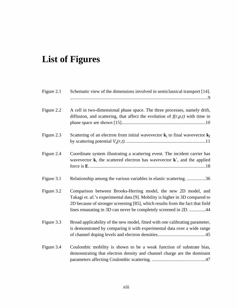
Figure 2.2 A cell in two-dimensional phase space. The three processes, namely drift,diffusion, and scattering, that affect the evolution of f(r,p,t) with time inphase space are shown [15]........................................................................10
Figure 2.3 Scattering of an electron from initial wavevector ki to final wavevector kfby scattering potential Vs(r,t). ....................................................................11
Figure 2.4 Coordinate system illustrating a scattering event. The incident carrier haswavevector k, the scattered electron has wavevector k´, and the appliedforce is E. ...................................................................................................18
Figure 3.1 Relationship among the various variables in elastic scattering. ................36
Figure 3.2 Comparison between Brooks-Herring model, the new 2D model, andTakagi et. al.’s experimental data [9]. Mobility is higher in 3D compared to2D because of stronger screening [85], which results from the fact that fieldlines emanating in 3D can never be completely screened in 2D. ..............44
Figure 3.3 Broad applicability of the new model, fitted with one calibrating parameter,is demonstrated by comparing it with experimental data over a wide rangeof channel doping levels and electron densities.........................................45
Figure 3.4 Coulombic mobility is shown to be a weak function of substrate bias,demonstrating that electron density and channel charge are the dominantparameters affecting Coulombic scattering. ..............................................47

xiv
Figure 3.5 Comparison between simulated and experimental IDS in subthreshold. Lackof the unscreened Coulomb term accounts for the discrepancy. ...............53
Figure 3.6 Comparison between extracted experimental data, new 2D model forunscreened Coulombic scattering, and 3D model due to Conwell andWeisskopf. .................................................................................................55
Figure 3.7 Comparison between experimental data and simulation results obtainedwithout a model for unscreened Coulombic scattering..............................57
Figure 4.1 Hierarchical taxonomy of the new semi-empirical local model. ...............64
Figure 4.2 Hierarchical taxonomy of lattice scattering. ..............................................67
Figure 4.3 Comparison between classical and quantum mechanical calculations ofelectron density in the inversion layer of MOSFETs.................................71
Figure 4.4 Thickness of the inversion layer as a function of transverse electric field. Atlow fields, classical formulation is required, whereas at high fields, quantummechanical formulation is applicable. .......................................................74
Figure 4.5 Illustrating the transition from 2D mobility to 3D mobility as one movesfrom the surface into the bulk. The assumption in this figure is that there issufficient gate bias to cause the 2D term at the interface to be less than the3D term (which is independent of the value of transverse electric field). .........................................................................................................................78
Figure 4.6 Illustrating the formation of energy subbands due to triangular wellconfinement of the electron gas near the Si-SiO2 interface.......................84
Figure 4.7 The transition function f(α) from 2D to 3D Coulombic mobility..............87
Figure 4.8 Comparison between Lombardi’s model and experimental data for threedifferent doping levels. Ideally, Lombardi’s model should have followedthe universal mobility curve shown by open circles for all three channeldoping levels. .............................................................................................97

xv
Figure 4.9 Comparison between the new model and the experimental universalmobility curve obtained by Takagi et. al. [9]. The new model exhibitsexcellent fits as channel doping is varied over three orders of magnitude. .....................................................................................................................100
Figure 4.10 Universal mobility curves obtained from the new model in equation (4.80)remain invariant to changes in oxide thickness and back gate bias. ........101
Figure 4.11 The generalized mobility curve shown here is the one that results whenCoulomb scattering due to channel dopants causes deviations from theuniversal mobility behavior. ....................................................................102
Figure 4.12 Variation of total mobility with distance from the interface for a MOSFETbiased in strong inversion. The cross section is taken at the center of thechannel. ....................................................................................................104
Figure 4.13 Variation of Coulombic mobility with distance from the interface for aMOSFET biased in strong inversion. The cross section is taken at the centerof the channel. ..........................................................................................105
Figure 4.14 Comparison between the simulated generalized mobility curve obtainedfrom the new local model (see equation (4.84)) and the experimentalgeneralized mobility curve obtained by Takagi et. al. [9]. ......................107
Figure 4.15 Comparison between simulated and experimental [96] generalized mobilitycurves over back gate bias. ......................................................................108
Figure 4.16 Comparison between the new 2D model for Coulombic scattering (seeequation (4.57)) and the 3D Brooks-Herring model [13]. B-H model is seento over- predict mobility since screening is stronger in 3D compared to2D.............................................................................................................109
Figure 5.1 Schematic cross-section of one half on an LDD MOSFET. The variouscomponents of the extrinsic resistance are shown. ..................................114
Figure 5.2 Doping and electron concentration profile in strong inversion for a 0.25µmAs-LDD MOSFET...................................................................................115

xvi
Figure 5.3 Quasi-Fermi potential drop along the Si/SiO2 interface of a 0.25µm As-LDD MOSFET in strong inversion. The drain bias is 100mV and the gatebias is 2.5V; hence the device is operating in the linear region. Although60% of the total resistance is due to the channel, a significant portion (40%)comes from the extrinsic region. The extrinsic resistance is primarily due toaccumulation layer resistance and spreading resistance. .........................116
Figure 5.4 Doping profile and electron concentration profile in strong inversion for a0.25µm As-LDD MOSFET. Compared to the doping profile shown inFigure 5.2, the length of the accumulation layer is longer because of thehigher diffusivity of phosphorus..............................................................117
Figure 5.5 Quasi-Fermi potential drop along the Si/SiO2 interface of a 0.25µm As-LDD MOSFET in strong inversion. The drain bias is 100mV and the gatebias is 2.5V; hence the device is operating in the linear region. Compared tothe potential drops shown in Figure 5.3, Ph-LDD devices exhibitconsiderably more accumulation layer resistance. Interestingly enoughthough, the spreading resistance is about the same in both cases............118
Figure 5.6 Existing technique for simulating an LDD MOSFET. Values for Rseries andLeff are typically obtained from experimental data, but invariably Rseries istreated as a calibrating parameter. ...........................................................120
Figure 5.7 Device schematic for simulating an LDD MOSFET. Rcontact informationshould be supplied from measurements such as from four-probe Kelvin teststructures. Patterned gate length should also obtained from experimentaldata such as from transmission electron microscopy of the gate stack.Neither Rcontact nor Lpatterned are used as fitting parameters in thissimulation scheme....................................................................................122
Figure 5.8 Proposed simulation methodology involves coupled 2D process and devicesimulations. The process recipe is fed to the process simulator to get the 2Ddoping profiles. Effective oxide thickness and contact resistance values aresupplied to the device simulator from independent measurements. Contact-to-poly spacing, Lcp, is obtained from layout information. .....................122
Figure 5.9 I-V characteristics for a 0.5µm x 0.5µm contact window. ......................124

xvii
Figure 5.10 Measured gate-to-channel capacitance for a 55Å gate oxide. Due to poly-depletion effect, the capacitance in accumulation is larger than that ininversion. Inversion-layer capacitance is further degraded due to thequantum-mechanical nature of the electron distribution. ........................126
Figure 5.11 Comparison between simulated and measured results in subthreshold for (a)0.25µm gate length, and (b) 0.3µm gate length, after gate lengths have beenreduced to achieve best fits. .....................................................................128
Figure 5.12 Simulation of a 0.25µm LDD MOSFET with a mobility model formulatedfor the inversion layer only. .....................................................................130
Figure 5.13 Hierarchical taxonomy of the unified model for inversion and accumulationlayer electrons. .........................................................................................131
Figure 5.14 Comparison between simulated and measured results for a 20.0µmMOSFET after adjustment of the surface roughness parameter. .............136
Figure 5.15 Comparison between simulation results and measured data in the linearregion for gate lengths ranging from 0.5µm to 0.25µm. It should be notedthat the fits for all the shown gate lengths are produced by one mobilityparameter set. ...........................................................................................137
Figure 5.16 Comparison between simulated and measured results in saturation forMOSFETs with gate length: (a) 0.25µm, (b) 0.3µm, (c) 0.4µm, (d) 0.5µm,and (e) 20.0µm.........................................................................................138

1
Chapter 1
Introduction
1.1 Motivation
As a result of MOS technology scaling over the last three decades, the complexity of
integrated circuits has increased tremendously from small-scale integration of a few
transistors on a silicon substrate to the ultra-large-scale integration (ULSI) of tens of
millions of transistors in today’s chips. The complexity associated with a ULSI circuit has
mandated the use of sophisticated computer-aided design (CAD) tools at all levels in the
design hierarchy — process, device, circuit, and system design respectively. It has been
recognized in recent years that the design of “integrated systems” (i.e. ULSI chips) would
entail a concurrent optimization of circuit architecture and device technology, which is
going to present new challenges for the CAD development community.
In previous chip generations, the circuit architecture was optimized independently of
technology. As a result, CAD tools were broadly divided into two categories:
electronic-design-automation (EDA) tools that included circuit and logic simulators,
layout editors, and logic synthesis tools primarily served the needs of the circuit and
system design community, whereas technology-CAD (TCAD) tools that included process
and device simulators were largely used by technologists. Regarding the use of tools, an
interesting distinction exists between the two communities. The circuit and system
designers rely heavily on the EDA tools for the design work since a system typically
involves a very large number of transistors. On the other hand, the use of TCAD tools by
the technologists has been limited, primarily because of its lack of predictivity, which
compels them to perform costly and time-consuming experiments to evaluate various

Chapter 1 Introduction 2
technology options. For the most part, TCAD tools serve the purpose of providing insight
into complex process and device physics phenomena that is not possible through
experimentation alone.
However, the scenario changes in the design of integrated systems. Since, a
simultaneous optimization of circuit and technology is desired, coupled device and circuit
simulations would need to be performed, thus making the device simulators an integral
part of the optimization and design loop. Hence, it has become important more than ever
that the TCAD tools be as predictive as possible, since circuits and systems would have to
be designed based on the data supplied by process and device simulators.
Predicitivity of TCAD tools hinges on the accuracy of models involved. The
challenge facing TCAD tool developers is the formulation and efficient numerical
implementation of physically-based models that exhibit a high degree of predictivity. To
this end, this thesis attempts to improve the accuracy of MOSFET simulations by
considering the modeling of one of the most important parameters affecting its I-V
characteristics — mobility of electrons in MOS inversion and accumulation layers.
This thesis focuses on issues related to mobility modeling in MOSFETs as they scale
to deep submicron dimensions. The aim is to extend the applicability of existing mobility
models by incorporating new physical effects that arise due to the scaling of MOS devices.
In this regard, two particular issues — Coulombic scattering and LDD resistance — have
been identified that require further modeling work, and are briefly discussed below.
Scaling of MOSFETs to deep submicron dimensions mandates an increase in
channel doping levels to suppress undesirable short-channel effects. One direct
consequence of increased doping is enhanced impurity scattering, fundamental treatment
of which is currently lacking in MOS inversion layers. The first half of the thesis is
devoted to a thorough examination of 2D Coulombic scattering and how it needs to be
modeled in the context of moment-based device simulators.
Traditionally, channel resistance has been the dominant factor limiting current
transport in MOSFETs. As a consequence, mobility models existing in literature only
addressed scattering in MOS inversion layers. However, in deep submicron MOSFETs
with LDD structures, parasitic series resistance has become comparable to channel
resistance, because of which it has become imperative to accurately model the extrinsic
region of the device. Thus, the mobility model developed in the first half of the thesis for
inversion layer electrons is extended to accurately model the accumulation layer occurring

Chapter 1 Introduction 3
in the extrinsic (parasitic) region of LDD MOSFETs.
1.2 Scope and Organization
Mobility models fall into one three broad categories: physically-based,
semi-empirical, and empirical. Physically-based models are those that are obtained from a
first-principles calculation, i.e. both the coefficients and the power dependencies
appearing in the model are obtained from a fundamental calculation. In practice,
physically-based models rarely agree with experimental data since considerable
simplifying assumptions are made in order to arrive at a closed form solution. Therefore,
to reconcile the model with experimental data, the coefficients appearing in the
physically-based model are allowed to vary from their original values. In this process the
power-law dependencies resulting from the first-principles calculation are preserved, and
the resulting model is termed as semi-empirical.
At the other end of the spectrum are empirically-based models in which the
power-law dependencies are also allowed to vary. Empirical models have less physical
content compared to the other two models, and also exhibit a narrower range of validity.
Empirical models are usually resorted to when the dependencies predicted by the
first-principles calculation do not allow a good fit between the experimental data and the
corresponding semi-empirical model.
The organization of this thesis is based on the following systematic methodology for
mobility modeling. The first step involves consideration of first principles calculation for
mobility. Then the coefficients appearing in the physically-based model are allowed to
vary in order to get a good fit between the model and experimental data. If this step is
successful, then the calibration procedure is complete, and the model is ready for
implementation in a device simulator. Otherwise, the power-law dependencies are also
allowed to vary until a good fit is obtained. In this case, the empirical model is then
implemented in the device simulator.
The objective of this thesis is to develop a semi-empirical model obtained from a
first-principles calculation. Since a first principles calculation is lacking for 2D Coulombic
scattering, it is discussed first. Chapter 2 provides the background material on the
calculation of mobility starting from the Boltzmann transport equation (BTE). The
machinery developed in Chapter 2 is then employed in Chapter 3 to calculate the

Chapter 1 Introduction 4
two-dimensional Coulombic mobility in MOS inversion layers due to scattering with
channel impurities. Separate calculations are performed for screened and unscreened
Coulombic scattering. A systematic extraction technique is also proposed for the
extraction of unscreened Coulombic mobility from experimental data, which in the case of
screened Coulombic mobility is taken from the literature. On comparison with
experimental data, it is shown that the new 2D model exhibits better agreement than
existing models for 3D Coulombic scattering.
Chapter 4 is concerned with the semi-empirical modeling of the inversion layer.
Extraction of semi-empirical models for phonon and surface roughness scattering from
first principles calculations is outlined. Based on the first principles model for Coulombic
scattering presented in Chapter 3, an empirical model for 2D Coulombic scattering is
extracted. The resulting model containing terms for phonon, surface roughness, and
Coulombic scattering is shown to accurately model experimental data over a wide range
of technology and bias conditions expressed in the form of a generalized mobility curve.
Finally, in Chapter 5, the importance of modeling mobility in the accumulation layer
is presented in the context of trying to accurately simulate deep submicron LDD
MOSFETs. To this end, the semi-empirical model for inversion-layer electrons is extended
to model the accumulation layer, and a systematic technique is presented for the validation
and calibration of the new model. A striking feature of the new model is that it exhibits
excellent agreement over a wide range of bias conditions in MOSFETs whose channel
length ranges from 20µm to 0.25µm. Very high confidence is placed in the predictive
nature of the new model since the same parameter set matches experimental data over
such a broad range.
Chapter 6 summarizes the conclusions of this research and offers suggestions for
future work.

5
Chapter 2
The BoltzmannTransport Equation
2.1 Introduction
A “first principles” calculation of macroscopic transport parameters such as mobility
starts with a description of the state of the electron gas in microscopic terms, and then
proceeds through a set of simplifying assumptions to arrive at the macroscopic parameter
that describes the state of the gas as a whole. Quantum-mechanically, the microscopic
state of the electron gas is described in terms of a many-body wavefunction, whereas
classically, it is described by specifying the position and momentum of each particle. To
characterize the operation of a MOSFET, we are not so much interested in the behavior of
each and every electron, rather we are interested in their collective motion. Thus, the
objective of performing the first-principles calculation is to filter out the essential piece of
information from the detailed microscopic description of the electron gas.
If we consider the inversion layer to be a classical ensemble, then its microscopic
state can be deterministically described by specifying the position and momentum of each
electron. Due to our lack of knowledge concerning the initial conditions, we have to resort
to a probabilistic description of the electron gas, which involves an N-particle distribution
function that gives the joint probability of finding the N particles at their respective
locations r with their respective momenta p. This description is still very detailed, and if
we assume the interactions among the electrons to be weak, and the time scales under
consideration to be much larger than the interaction time between electrons, then the

Chapter 2 The Boltzmann Transport Equation 6
N-particle distribution function can be reduced to a single particle distribution function.
Thus, we postulate that under these simplifying assumptions, the single particle
distribution function f(r,p,t) describes the collective state of the electron gas. The
evolution of f(r,p,t) with time is governed by the Boltzmann transport equation (BTE)
which forms the cornerstone of semiclassical electron dynamics.
In this chapter, we present a methodology for calculating mobility µ from the
Boltzmann transport equation. The BTE is a complex integro-differential equation that is
based on both quantum-mechanical and classical laws of dynamics. As such, the BTE in
its original form does not yield a closed form solution for mobility, and simplifying
assumptions are necessary to make the solution tractable. A detailed discussion of the
assumptions made is presented in this chapter, which is organized into three main sections.
The first part, Section 2.2, deals with the derivation and simplification of the BTE.
Derivation of the classical part is discussed earlier on in Section 2.2, while Section 2.2.1 is
devoted to setting up the collision integral based on quantum mechanical principles.
Section 2.2.2 presents a very important simplification to the collision integral, known as
the relaxation time approximation (RTA). RTA permits us to calculate a closed form
expression for mobility. Because of its significance, it is important to know the conditions
under which the RTA is applicable. This forms the subject of discussion in Section 2.2.3.
Thus, by the end of Section 2.2, we have a simplified form of the BTE that permits us to
arrive at a closed form solution for mobility.
In Section 2.3, we discuss the approximations and outline the method for calculating
mobility from the BTE using the RTA. This section concludes with an expression for
mobility that has the relaxation time as a parameter.
Finally Section 2.4 discusses the quantum mechanical calculation of the relaxation
time from the scattering potential. This calculation is based on the Fermi’s golden rule that
is derived from first-order time-dependent perturbation theory.
Thus the methodology that is presented in this chapter allows one to calculate
mobility from a knowledge of the scattering potential. Calculation of the scattering
potential forms the subject of the next chapter in which we first calculate the scattering
potential for a screened two-dimensional Coulombic center, and then employ the
machinery developed in this chapter to calculate the Coulombic mobility from the
scattering potential.

Chapter 2 The Boltzmann Transport Equation 7
2.2 Boltzmann Transport Equation
The classical theory of transport processes is based on the Boltzmann transport
equation, which specifies the temporal evolution of the single-particle distribution
function f(r,p,t) in the six-dimensional phase space of Cartesian coordinates r and
momentum p , and it is defined by the relation
(2.1)
Since trajectories in phase space do not intersect, Liouville’s theorem states that the
probability density of points in phase space remains constant in time, provided there is no
scattering. Thus, in the 6 dimensional phase space [83]:
(2.2)
In the presence of scattering, the total rate of change of f(r,p,t) with time equals the rate of
scattering. Equation (2.2) thus transforms into:
(2.3)
Expanding the total derivative in equation (2.3) yields:
(2.4)
Equation (2.4) is the celebrated Boltzmann’s transport equation (BTE) [16], which finds
applications in diverse areas such as neutron transport in reactors, propagation of light
through stellar matter, plasma dynamics, rarified gas dynamics, and electron transport in
metals and semiconductors [17]. The rate of change of momentum is equal to the
applied force F, and in the absence of a magnetic field, it is simply given by Lorentz’s law:
(2.5)
f r p,( ) drdp probability of finding a particle in drdp=
df r p t, ,( )dt
------------------------- 0=
df r p t, ,( )dt
-------------------------f∂t∂
----
coll=
f∂t∂
---- r ∇ rf⋅ p ∇ pf⋅+ +f∂t∂
----
coll=
p
p F qE r t,( )= =

Chapter 2 The Boltzmann Transport Equation 8
The rate of change of distance with time is equal to the group velocity of Bloch1
electrons [14]. Thus, the BTE for the Bloch electrons can be written as:
(2.6)
While the left hand side of equation (2.6) is a classical description of electron motion, the
collision term on the right side requires a quantum treatment, which we discuss next.
2.2.1 Treatment of the Scattering Term
Electrons in solids are commonly represented by wave packets, and according to
Heisenberg’s uncertainty principle, they have a certain amount of spread in both real and
momentum space. Typically, the extent of spread in real space is of the order of a few
lattice constants. Usually, the externally applied potentials vary over hundreds of lattice
constants, and to a very good approximation these potentials can be considered as constant
over the dimensions of a wave packet. In such a scenario, the interaction between the
electron and the external potential can be treated according to the classical laws of
dynamics. On the other hand, if the variation in potential is of the order of the spread of a
wavepacket, then this interaction needs to be treated quantum mechanically via the
single-electron Schrodinger’s equation.
Clearly, the periodic potential due to the atomic cores, i.e. the nuclei, varies on the
order of a lattice constant, and hence this interaction needs to be treated quantum
mechanically. When Schrodinger’s equation is solved with this periodic potential, one
finds that the electrons can be treated as “free” particles travelling with an effective mass
that is different from the free electron2 mass. The effective mass approximation fails if the
externally applied field varies very rapidly, since that field can no longer be treated in the
classical framework, and instead needs to be included in Schrodinger’s equation. Thus, for
the left hand side in equation (2.6) to be valid, the externally applied electric fields have to
vary slowly compared to the dimensions of a wavepacket, as illustrated in Figure 2.1 [14].
1. Electrons moving in a periodic potential and satisfying the single-electron Schrodinger’s equationare known as Bloch electrons [14].
2. A free electron, by definition, is one that moves in a zero potential field.
r
f∂t∂
---- vg ∇ rf⋅ qE ∇ pf⋅+ +f∂t∂
----
coll=
Chapter 2 The Boltzmann Transport Equation 9
However, when electrons scatter off an imperfection in a semiconductor, the spatial
extent of the interaction potential is of the same order of magnitude as the dimensions of a
wavepacket. That is why all collision events need to be considered quantum mechanically.
While the “free” flight of electrons between two collision events is treated classically, the
collision event itself is treated quantum mechanically.
In an effort to model the collision term, we examine in greater detail its role in the
BTE. The left hand side of equation (2.6) governs the evolution of the distribution
function f(r,p,t) with time at a point (r,p) in phase space due to externally applied forces,
whereas its right hand side accounts for the effect of random scattering events on f(r,p,t).
The various contributions are seen more clearly if equation (2.6) is rewritten as follows:
(2.7)
Then, the local rate of change of f(r,p,t) with time at a point (r,p) in phase space is given by
the sum of the three terms: the first term represents the effect of diffusion due to spatial
gradients in f(r,p,t); the second term represents the effect of drift due to the externally
applied field E, and the last term represents the effect of scattering events on f(r,p,t). These
wavelength of applied field
Profile of applied field
Profile of Electron wavepacket
Spread ofwavepacket
LatticeConstant
Figure 2.1 Schematic view of the dimensions involved in semiclassical transport[14].
r
f∂t∂
---- vg ∇ rf⋅( )–= qE ∇ pf⋅( )–f∂t∂
----
coll+
Chapter 2 The Boltzmann Transport Equation 10
various processes are depicted graphically in Figure 2.2.
If we consider a small volume in phase space centered around the point (r,p) (see
Figure 2.2), then some particles would be leaving this volume due to out-scattering, while
others would be entering it due to in-scattering. It should be noted that a scattering event
abruptly changes the momentum of the particle without changing its position. The net
effect of scattering on the number of particles in the volume element is simply the
difference between the number of in-scattered and out-scattered particles:
(2.8)
Since the details of the scattering event need to be treated quantum mechanically, the
In-scattering
Out-scattering
In-flow Out-flowf(r).vg f(r+dr).vg
p
p+dp
r r+dr
In-flow
Out-flowf(p+dp).qE
f(p).qEr
p
Figure 2.2 A cell in two-dimensional phase space. The three processes, namely drift,diffusion, and scattering, that affect the evolution of f(r,p,t) with time in phase space areshown [15].
(Drift)
(Diffusion)
f∂t∂
----
collIn scattering rate( ) Out scattering rate( )–=
f∂t∂
----
coll
in f∂t∂
----
coll
out–=
Chapter 2 The Boltzmann Transport Equation 11
electron is specified in terms of its Bloch wavefunction which is characterized by
quasi-continuous momentum eigenvalues p, or equivalently the wavevector k in
momentum space, where . In addition to the k vector, the Bloch wavefunction is
also characterized by a band index; however, this parameter would be ignored since it will
be assumed that scattering events are strictly intraband. Thus, Bloch wavefunctions take
on the following form [14]:
(2.9)
where u(r) is a periodic function such that u(r+R)=u(r), where R is the periodicity of the
lattice. An electron incident on a scattering center with wavevector ki would emerge with
wavevector kf , and if kf is different from ki , the electron is said to have been scattered,
while kf = ki implies that the electron emerges unscattered. Scattering centers typically
result from perturbations in the background electrostatic potential, and are characterized
by a scattering potential Vs(r,t). Scattering potential may be well localized in space, as in
Coulombic scattering, or it may extend throughout the crystal, as in phonon scattering. A
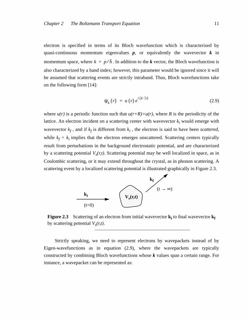
scattering event by a localized scattering potential is illustrated graphically in Figure 2.3.
Strictly speaking, we need to represent electrons by wavepackets instead of by
Eigen-wavefunctions as in equation (2.9), where the wavepackets are typically
constructed by combining Bloch wavefunctions whose k values span a certain range. For
instance, a wavepacket can be represented as:
k p h⁄=
ψk r( ) u r( ) ei k r⋅( )
=
Vs(r,t)ki
kf
(t=0)
(t → ∞)
Figure 2.3 Scattering of an electron from initial wavevector ki to final wavevector kfby scattering potential Vs(r,t).

Chapter 2 The Boltzmann Transport Equation 12
(2.10)
where c(k,ko) is a function centered around ko, and goes to zero if k is far from ko. A
candidate function for instance could be a Gaussian distribution centered around ko.
The property of the wavepacket in equation (2.10) is that it is localized in space at
the expense of a spread in momentum space (i.e. this wavepacket does not have a
well-defined momentum). On the other hand, the Eigen-wavefunction in equation (2.9)
exhibits a definite momentum but is not localized in space, and thus not really
representative of an electron travelling in a solid. Nevertheless, we shall work with
Eigenfunctions as in equation (2.9) since it is too cumbersome to work with wavepackets.
In order to find the rate at which electrons scatter into or scatter out of an element in
phase space, we first need to know the probability per unit time, also known as the
transition rate S(k,k´), with which an electron in state ki would scatter to a state kf in unit
time. The probability that a scattering event does take place also depends upon the number
of electron present in the initial state and the availability of the final states. Pauli’s
exclusion principle for fermions (which includes electrons) prohibits more than two of
them from occupying the same eigenstate. Thus, an arbitrary number of electrons can not
occupy a given state even if one exists. Hence, the probability of scattering per unit time
from k to k´, also known as the scattering rate, is given by:
(2.11)
The probability per unit time that an electron initially in state k would scatter out to any
possible k state is known as the total scattering rate, and is obtained from equation (2.11)
by summing over all the possible final k´ vectors:
(2.12)
The summation over k space can be converted to integration in k space by introducing the
density of states in k space D(k)=V/(2π)3, where the number of k states in dk is D(k)dk,
and V is the volume of the crystal. Assuming that scattering does not flip spin, we get:
Ψ r t,( ) c k ko,( ) ψk r( ) e
i
h---ε k( ) t–
kd
∞–
∞
∫=
P k k'→( ) S k k',( ) f k( ) 1 f k'( )–[ ]=
P k( ) S k k',( ) f k( ) 1 f k'( )–[ ]k'∑=

Chapter 2 The Boltzmann Transport Equation 13
(2.13)
Pout(k) thus corresponds to the probability of scattering out of state k in unit time, i.e.
. Conversely, the scattering rate from k´ to k is given by:
(2.14)
and the total scattering rate into state k is given by:
(2.15)
Pin(k) thus corresponds to the probability of scattering into state k in unit time, i.e.
. Therefore, the net change in the distribution function due to
scattering is given by the difference Pin(k)-Pout(k):
(2.16)
Equation (2.16) is commonly known as the collision integral. S(k,k´) appearing in the
collision integral is obtained from the scattering potential Vs(r,t) via a
quantum-mechanical calculation which is outlined in greater detail in Section 2.4.
Replacing the right-hand side of the BTE in equation (2.6) with the collision integral, it
now reads:
(2.17)
Equation (2.17) is an integro-differential equation in f(r,p,t), and clearly simplifications are
required in order to make the solution tractable. In the next section, we discuss one such
Pout k( ) V
2π( ) 3--------------- S k k',( ) f k( ) 1 f k'( )–[ ] k'd∫=
Pout k( ) f∂f∂
----
coll
out=
P k' k→( ) S k' k,( ) f k'( ) 1 f k( )–[ ]=
Pin k( ) V
2π( ) 3--------------- S k' k,( ) f k'( ) 1 f k( )–[ ] k'd∫=
Pin k( ) f∂f∂
----
coll
in=
f∂t∂
----
coll
V
8π3--------- S k' k,( ) f k'( ) 1 f k( )–[ ] S k k',( ) f k( ) 1 f k'( )–[ ]– k'd∫=
f∂t∂
---- vg ∇ rf⋅ qE ∇ pf⋅+ +
V
8π3--------- S k' k,( ) f k'( ) 1 f k( )–[ ] S k k',( ) f k( ) 1 f k'( )–[ ]– k'd∫=

Chapter 2 The Boltzmann Transport Equation 14
simplification to the collision integral, known as the relaxation time approximation.
2.2.2 The Collision Integral in the Relaxation Time Approximation
The collision integral as it stands in equation (2.16) makes equation (2.17) a
complex integro-differential equation whose solution under the most general conditions is
not possible. In the relaxation time approximation (RTA), the collision integral is replaced
by an algebraic equation that involves a parameter known as the relaxation time τ :
(2.18)
where f is the distribution function that needs to be determined and fo is the equilibrium
distribution function (Maxwell-Boltzmann for non-degenerate gases and Fermi-Dirac for
degenerate gases). The physical interpretation of equation (2.18) is that the scattering rate
is proportional to the deviation from equilibrium f-fo, and inversely proportional to the
relaxation time (i.e. if τ is short, scattering rate would be high). Since scattering tends to
return a system to equilibrium, τ represents the characteristic time over which a system
relaxes back to equilibrium after an excitation has been removed. Since the RTA is a
useful approximation to the BTE, the next section critically examines the conditions under
which equation (2.18) is a valid approximation to the collision integral in equation (2.16).
2.2.3 Validity of the Relaxation Time Approximation
In Section 2.2.1, a formulation for was presented (see equation (2.16))
that involved the quantum-mechanical entity S(k,k´). In Section 2.2.2, a relaxation time
approximation to the collision integral was postulated that would considerably simplify
solving the BTE. In this section, we discuss the conditions under which the RTA is valid
and also show how the relaxation time τ is calculated from the transition rate S(k,k´). In
Section 2.3 we will show how the calculation of mobility µ proceeds from the BTE once τis known. Finally, in Section 2.4, we outline the quantum-mechanical calculation of
S(k,k´) from first-order time-dependent perturbation theory.
We start by expressing the non-equilibrium distribution function f as the sum of a
symmetric and an asymmetric part:
f∂t∂
----
coll
f fo–
τ-----------–=
f∂ t∂⁄[ ] coll

Chapter 2 The Boltzmann Transport Equation 15
(2.19)
where fs is symmetric and fa is asymmetric in momentum. The benefit of splitting up f in
this way is that fs cannot cause any current flow due to its symmetrical nature, since there
are equal number of carriers moving in opposite directions. Hence, any contribution to
current would come from a non-zero fa . The collision integral can also be split up as:
(2.20)
The first simplification is to assume a non-degenerate semiconductor, i.e f << 1. Then all
the [1-f] terms appearing in the collision integral in equation (2.16) reduce to unity.
Hence, we get:
(2.21)
and
(2.22)
In equilibrium, fs = fo, and hence . Thus, from equation (2.21) we find
that at equilibrium, S(k´,k) = S(k,k´), i.e. forward and backward transitions occur with
equal probability1. Even under non-equilibrium conditions, if the applied fields are weak,
the deviation from equilibrium is small, and the principle of detailed balance remains
applicable. Moreover, fs ≈ fo under such conditions, and it is reasonable to assume that
. The collision term then reduces to:
(2.23)
1. Commonly known as the principle of detailed balance [18].
f fs fa+=
f∂t∂
----
coll
fs∂t∂
------
coll
fa∂t∂
-------
coll+=
fs∂t∂
------
coll
V
8π3--------- S k' k,( ) fs k'( ) S k k',( ) fs k( )– k'd∫=
fa∂t∂
-------
coll
V
8π3--------- S k' k,( ) fa k'( ) S k k',( ) fa k( )– k'd∫=
fs∂ t∂⁄[ ]coll
0=
fs∂ t∂⁄[ ]coll
0=
f∂t∂
----
coll
V
8π3--------- S k k',( ) fa k'( ) fa k( )–[ ] k'd∫=

Chapter 2 The Boltzmann Transport Equation 16
Equation (2.23) is still complicated because it is a functional of fa . We need to arrive at a
form for that would make it proportional to fa , not a functional of fa .
Since integration in equation (2.23) is being carried over k´, we can rewrite it as follows:
(2.24)
If the first integral term on the right hand side of equation (2.24) vanishes, then the
collision term would become proportional to fa as desired. Since fa(k´) is an odd function
of k´, if S(k,k´) can be shown to be an even function of k´, then their product would be an
odd function of k´, and hence the integral would vanish when integrated over k´. S(k,k´)
gives the probability that an electron in state k would scatter to state k´. For Bloch
electrons, . Hence, a velocity-randomizing scattering event is one in which
an electron incident on the scattering center with velocity vi has an equal probability of
scattering off in any direction (i.e. S(k,k´)=S(k,-k´) which implies that k´ and -k´ are
equally probable final states). Thus, for a given value of k, all values of k´ are equally
probable, implying that S(k,k´) is an even function of k´. That is why velocity randomizing
collisions are also known as isotropic scattering events, since all angles after scattering are
equally probably — the direction of the final wavevector is independent of the direction of
the incident wavevector. Collisions with phonons are typically isotropic, whereas those
with Coulombic centers are not. Thus, for isotropic scattering, the collision integral takes
on the simple form:
(2.25)
Going back to the definition of the RTA in equation (2.18), we have:
(2.26)
Equating (2.25) and (2.26), the relationship between τ and S(k,k´) is then given by:
f∂ t∂⁄[ ] coll 0=
f∂t∂
----
coll
V
8π3--------- S k k ′,( ) fa k ′( ) k ′d∫ V
8π3--------- fa k( ) S k k',( ) k'd∫–=
vg hk m∗⁄=
f∂t∂
----
coll
V
8π3---------– fa k( ) S k k',( ) k'd∫=
f∂t∂
----
coll
f fo–
τ k( )------------–
fa k( )τ k( )
---------------–= =

Chapter 2 The Boltzmann Transport Equation 17
(2.27)
The fact that τ in equation (2.27) is independent of f implies that the collision integral in
equation (2.16) can be effectively reduced to the algebraic expression in equation (2.18).
The approximations and assumptions made in reducing equation (2.16) to equation (2.25)
are collectively referred to as the relaxation time approximation or RTA.
A velocity randomizing collision is not the only type of scattering event that is
compatible with the RTA. Here, we discuss another type of scattering event, namely an
elastic collision, that can treated in the RTA. For arbitrary electric field strengths, the
non-equilibrium distribution function f(k) can be expanded in a series of spherical
harmonic functions [41], [42]:
(2.28)
where θ is the angle between the electron wave vector k and the applied electric field, and
ε is the electron energy given by . The unknown functions fm(ε) need to
be solved for by substituting for f in the BTE. The rationale for this choice of expansion is
that the electric field is a symmetry-breaking operator that introduces a preferred axis (i.e.
the direction of the electric field) along which a shift of the distribution function occurs.
On the other hand, there is no breaking of symmetry in the azimuthal plane around the
electric field vector, so that the polar angle becomes a good expansion function for the
cylindrical symmetry of the problem. For low applied electric fields, the perturbation
would be weak, and thus the series may be terminated after the second term to give:
(2.29)
Thus, according to our definition, . Substituting for fa in
equation (2.23) gives:
(2.30)
1τ k( )------------
V
8π3--------- S k k',( ) k'd∫=
f k( ) fm ε( ) Pm θcos( )m 0=
∞
∑ fo ε( ) Po θcos( ) f1 ε( ) P1 θcos( ) . . .+ += =
ε hk( )2
2m∗⁄=
f k( ) fo k θcos f1 ε( )⋅ ⋅+=
fa k( ) k θcos f1 ε( )⋅ ⋅=
f∂t∂
----
coll
V
8π3---------f1 ε( ) k θ S k k',( )
f1 ε'( ) k' θ'cos
f1 ε( ) k θcos-------------------------------- 1– k'd∫cos=

Chapter 2 The Boltzmann Transport Equation 18
If scattering is elastic, then and . Note that . Then equation (2.30)
reduces to:
(2.31)
Therefore, if we define relaxation time as
(2.32)
the collision integral takes on the familiar form . Equation (2.32) can
be simplified further if we assume spherical bands. Figure 2.4 represents the coordinate
system illustrating a scattering event. We are interested in finding the relationship among
α (the angle between k and k´), θ, and θ´ . Using the expression for dot product between
two vectors r1•r2=|r1| |r2| cos(θ), we get for cos(θ´):
ε' ε= k' k= k' k≠
f∂t∂
----
coll
V
8π3---------– fa k( ) S k k',( ) 1 θ'cos
θcos-------------– k'd∫=
1τ k( )------------
V
8π3--------- S k k',( ) 1 θ'cos
θcos-------------– k'd∫=
f∂t∂
----
coll
fa k( )τ k( )--------------–=
x
z
y
k
k´
Eθ
α
φ
k = k uz
k´ = k ( sinα cosφux + sinα sinφuy + cosα uz )
E = E ( sinθ uy + cosθ uz )
Figure 2.4 Coordinate system illustrating a scattering event. The incident carrier haswavevector k, the scattered electron has wavevector k´, and the applied force is E.
θ´
Chapter 2 The Boltzmann Transport Equation 19
(2.33)
and hence,
(2.34)
For spherical bands, S(k,k´) is independent of φ; hence, sinφ would integrate to zero,
leaving the cosα term. Thus, relaxation time can be expressed more simply as:
(2.35)
In summary, the assumptions under which the relaxation time approximation holds are:
(1) Non-degenerate semiconductor.
(2) Low applied fields, i.e. carrier temperature ≈ lattice temperature.
(3) Deviation of the distribution function from equilibrium is small.
(4) Collisions are either velocity randomizing or elastic.
(5) If collisions are elastic, then energy bands must be spherical.
2.3 Calculation of Mobility from the BTE in the RTA
The relaxation time approximation to the collision integral allows us to solve for the
non-equilibrium distribution function f(r,k,t) for some special cases of interest. An
important parameter appearing in the solution f(r,k,t) is the relaxation time, which is
calculated from either equation (2.27) or (2.35) as discussed in the previous section.
Equations (2.27) and (2.35) in turn need to know the transition rate S(k,k´), which is
calculated quantum mechanically from first-order time-dependent perturbation theory. In
the next section, we show how S(k,k´) can be calculated if the nature of the interaction
between the electron and the scattering center is known.
Once f(r,k,t) is known, it is possible to calculate macroscopic transport coefficients
such as mobility and thermal conductivity. In this section, we show how the low-field
mobility is calculated from the BTE using the RTA.
E k'⋅E k'-------------- θ'cos θ α φsinsinsin θ αcoscos+= =
θ'cosθcos
------------- θ α φsinsintan αcos+=
1τ k( )------------
V
8π3--------- S k k',( ) 1 αcos–[ ] k'd∫=

Chapter 2 The Boltzmann Transport Equation 20
The expression for the convective current density1 vector is given by
(2.36)
where , and <v(r)> is the average velocity vector at point r. Since the
average is over the ensemble of particles, the average velocity is calculated by weighting
it with the non-equilibrium distribution function f(r,k,t). Therefore, in terms of the
distribution function, the expression for J takes on the following form:
(2.37)
where f(r,k,t)=fs(r,k,t)+fa(r,k,t) as given in equation (2.19). Since the symmetric part of the
distribution function does not contribute to current2, equation (2.37) reduces to:
(2.38)
In order to proceed with the calculation of J, we first need to evaluate the non-equilibrium
distribution function f(r,k,t) from the BTE using the RTA, which assumes the form:
(2.39)
In steady state, , and if we further assume a spatially homogeneous
semiconductor, as well. The asymmetric part of the distribution fa is then given
by:
1. Convective current density is due to flow of particles. This is contrasted with the displacementcurrent density which is due to the rate of change of electric field with respect to time at a certainpoint in space.
2. For the symmetric part of the distribution function, fs(r,k,t)=fs(r,-k,t); hence, there are as manycarrier moving to the right as there are to the left. Therefore, net movement of the carriers is zero.
J qn v r( )⟨ ⟩=
J Jxi Jyj Jzk+ +=
J 2q
2π( ) 3--------------- vf r k t, ,( ) kd∫=
J 2q
2π( ) 3--------------- vfa r k t, ,( ) kd∫=
f∂t∂
---- vg ∇ rf⋅ qE fp∇⋅+ +fa k( )τ k( )--------------–=
f∂ t∂⁄ 0=
fr∇ 0=

Chapter 2 The Boltzmann Transport Equation 21
(2.40)
Relaxation time approximation holds under the condition that f should not deviate
significantly from fo. By replacing f by fo in the momentum-space gradient, and with a
change of variables, we get:
(2.41)
Therefore, fa takes on the following form:
(2.42)
Hence, J is now given by:
(2.43)
According to Ohm’s law, . In tensor form, J is given by:
(2.44)
Equating (2.43) and (2.44), we see that an entry in the conductivity tensor is given by:
(2.45)
For elastic scattering mechanisms |k|=|k´|, and hence the transition rate is independent of
the initial direction of the wavevector k since S(k,k´)=S(k-k´)=S(|k|,θ). Thus, τ(k) can be
expressed as τ(ε). Moreover, if the band structure is assumed to be isotropic, the
fa k( ) τ k( ) qEh
------- fk∇⋅–=
fk∇ fok∇≈ ε∂∂fo ε k( )k∇⋅ h ε∂
∂fov= =
fa k( ) qτ k( ) ε∂∂fo v E⋅( )–=
Jq
4π3--------- τ k( ) ε∂
∂fov v E⋅( ) kd∫–=
J σE=
Jx
Jy
Jz σxx σxy σxz
σyx σyy σyz
σzx σzy σzz
Ex
Ey
Ez
=
σijq
4π3--------- τ k( ) ε∂
∂fovivj kd∫–=

Chapter 2 The Boltzmann Transport Equation 22
conductivity tensor becomes diagonal [60]. Thus, any one component on the diagonal is
given by:
(2.46)
where i=x, y, or z, and µ is the mobility. Assuming Maxwell-Boltzmann statistics,
, which implies that . Given that the electron concentration
n can be written as:
(2.47)
the expression for mobility1 becomes:
(2.48)
Since we are dealing with an isotropic band structure, we can perform the integration over
the scalar ε instead of the vector k. For an isotropic band structure, the constant energy
surfaces are spherical, i.e. . The density of states in energy is defined as:
(2.49)
From the equipartition of energy, , and
1. In semiconductors, mobility is treated separately from conductivity since n can vary by orders ofmagnitude in doped semiconductors, and µ can vary independently of n. However, in metals, n isconstant and very high, and conductivity is taken to be synonymous with mobility.
σi qnµ q
4π3--------- τ ε( ) ε∂
∂fovi2
kd∫–= =
fo eε kT⁄–∝ fo ε∂⁄∂ fo kT⁄–=
n r t,( ) 1
4π3--------- f r k t, ,( ) kd∫=
µ
q
4π3--------- τ ε( )
fo
kT------vi
2kd∫
1
4π3--------- fo kd∫
--------------------------------------------=
ε hk( )2
2m∗⁄=
D ε( ) dε No. of states in dε Crystal Volume⁄=
Vol in k-space corresponding to dε( ) D k( )⋅[ ] Vol⁄=
dk1
4π3---------⋅=
v2
vx2
vy2
vy2
+ + 3vi2
= =

Chapter 2 The Boltzmann Transport Equation 23
. Changing the variable of integration from k to ε and
substituting for , the expression for mobility in equation (2.48) simplifies to:
(2.50)
Since , and in 3D, , the expression for mobility in
equation (2.50) becomes:
(2.51)
If we define , and are able to express τ(ε) as
(2.52)
then,
(2.53)
Now, , where and .
Therefore, equation (2.53) can be rewritten as:
ε 1 2⁄( ) m∗ v2
3 2⁄( ) m∗ vi2
= =
vi2
µq τ ε( )
fo
kT------ 2ε
3m∗----------
4π3D ε( ) εd∫
fo4π3D ε( ) εd∫
--------------------------------------------------------------------------=
fo eε kT⁄–∝ D ε( ) 2m∗( )
3 2⁄
2π2h
3-------------------------ε1 2⁄
=
µ
qm∗------- ε
kT------
τ ε( ) e
εkT------– ε
kT------
1 2⁄ εkT------
d∫32--- e
εkT------– ε
kT------
1 2⁄ εkT------
d∫--------------------------------------------------------------------------------------=
x ε kT⁄≡
τ ε( ) τoε
kT------
s⋅=
µ
qτo
m∗--------
x
32--- s+
ex–
xd∫32--- x
1 2⁄e
x–xd∫
-------------------------------------------------=
ex–x
sxd
0
∞
∫ Γ s 1+( )= Γ 1 2⁄( ) π= Γ s 1+( ) sΓ s( )=

Chapter 2 The Boltzmann Transport Equation 24
(2.54)
Equation (2.54) specifies the relationship between the momentum relaxation time τ(ε) and
mobility µ. Momentum relaxation time when expressed as τ(ε) specifies the time it would
take for an electron with energy ε to randomize its initial momentum. Since electrons in a
system are distributed in energy, electrons with different energies would take different
times to randomize their initial momentum. Mobility can thus be viewed as being
proportional to the average time it takes the electron gas to randomize its initial
momentum.
In summary, starting with Boltzmann’s transport equation as given in equation
(2.17), the following assumptions and simplifications allow us to derive an expression for
low-field mobility:
(1) In the relaxation time approximation, the collision integral in equation (2.16)
can be reduced to the simplified form in equation (2.26) provided the collisions
are either elastic (as in Coulomb scattering) or velocity randomizing (as in
acoustic phonon scattering).
(2) An implicit assumption in the RTA is that the non-equilibrium distribution
function f is only slightly perturbed from the equilibrium distribution function
fo. Hence .
(3) Maxwell-Boltzmann statistics is assumed, which is consistent with the
assumption underlying the derivation of the BTE that the gas should be weakly
interacting. If the gas is dense, then due to strong interactions among the
particles, the single-electron distribution function f(r,p,t) loses its validity.
(4) Momentum relaxation time is assumed to be independent of the direction of the
wavevector of the incident electron. This can only be true if the scattering
event is elastic, i.e. which implies that the
transition rate depends upon the speed with which the carriers approach the
scattering potential and the angle through which they are deflected. Under this
simplification, τ(k) can be written as τ(ε).
(5) The band structure is assumed to be spherical (i.e. isotropic) and parabolic.
The assumption of isotropy allows us to perform integrations over the scalar
µqτo
m∗-------- Γ s 5 2⁄+( )
Γ 5 2⁄( )-----------------------------⋅=
fk∇ fok∇≈
S k k ′,( ) S k k ′–( ) S k θ,( )= =

Chapter 2 The Boltzmann Transport Equation 25
quantity ε as opposed to the vector quantity k.
Thus, the calculation of mobility in equation (2.54) starting with the momentum
relaxation time τ(ε) is a purely classical calculation since it involves the use of the
classically-described distribution function f(r,k,t). Momentum relaxation time can be
calculated from either equation (2.27) or equation (2.35). In either case, we need to know
the transition rate S(k,k´) first, calculation of which is based on purely quantum
mechanical terms. We discuss this calculation in the next section. The mix of quantum and
classical calculations in calculating the macroscopic transport parameter mobility is what
makes this particular treatment semi-classical in nature.
2.4 Calculation of the Transition Ratefrom Perturbation Theory
In this section, we draw the connection between the transition rate S(k,k´) and
scattering potential which describes the potential field created by the scattering
center. It is the interaction of an electron with the scattering potential that is
phenomenologically known as an scattering event, and mathematically described through
time-dependent perturbation theory as we discuss next.
At the fundamental level, Schrodinger’s equation describes the interaction of the
electrons with various forces, or equivalently potential fields, appearing in the solid:
(2.55)
The crystal potential, , is periodic in nature and it describes the electrostatic
potential due to the atomic cores. describes potentials that are built-in or applied
to the device, while describes the scattering potential due to random deviations
in potential that may be caused by ionized impurities or lattice vibrations. As discussed in
Section 2.2.1, applied potentials are treated classically, and hence need not be
considered in equation (2.55). Even with this simplification, it is not possible to solve
equation (2.55). We make another simplification by neglecting under the
Vs r t,( )
iht∂
∂ΨVc r( ) Va r t,( ) Vs r t,( )+ +[ ] Ψ h
2
2m------- ∇ 2Ψ–=
Vc r( )
Va r t,( )
Vs r t,( )
Va r t,( )
Vs r t,( )

Chapter 2 The Boltzmann Transport Equation 26
assumption that it is much smaller than . The resulting equation yields the
well-known Bloch wavefunction as its solution, described by equation (2.9).
Since , it is treated as a small perturbation to . The effect of
such a perturbation is to cause an electron initially in Bloch state to make a
transition to another Bloch state . The rate of transition S(k,k´) is given by the
Fermi’s Golden Rule [70] that is derived from first-order time-dependent perturbation
theory [70]:
(2.56)
The rate of transition quadratically depends upon how strongly the scattering potential Vs
couples the two Bloch states Ψi and Ψf . This coupling is expressed through the matrix
element <Ψf | Vs | Ψi >. The delta function appearing in equation (2.56) expresses the
conservation of energy during the scattering process.
The task that finally remains is identifying the nature of the scattering potential
Vs(r) . The discussion so far is applicable to all kinds of scattering mechanisms. However,
calculation of Vs(r) specifically depends upon the nature of the scattering process. In the
next chapter, we shall discuss in considerable detail how to set up Vs for a
two-dimensional Coulombic potential that is screened by a two-dimensional electron gas.
Once Vs has been calculated, we shall use the machinery developed in this chapter to
calculate the mobility for two-dimensional Coulombic scattering.
More commonly, the Fourier transform of the scattering potential Vs(q) is easier to
calculate than Vs(r) itself. As we shall show, it is not necessary to convert back to real
space r since we can very well work in its Fourier space representation.
When the matrix element is expressed in the coordinate-space
representation, we get:
(2.57)
Vc r( )
Vs r t,( ) Vc r( )« Vc r( )
Ψi r t,( )
Ψf r t,( )
S k k ′,( ) 2πh
------ Ψf⟨ |Vs Ψi| ⟩ 2 δ ε kf( ) ε ki( )–[ ]=
Ψf⟨ |Vs Ψi| ⟩
Ψf⟨ |Vs Ψi| ⟩ Ψf∗ r( ) Vs r( ) Ψi r( ) rd
v∫=

Chapter 2 The Boltzmann Transport Equation 27
The Fourier series expansion of Vs(r) is given by , where the
Fourier coefficients are given by . For Bloch electrons,
. Hence, equation (2.57) becomes [59]
(2.58)
Since the integral is zero except when , equation (2.58) simplifies to
(2.59)
For parabolic bands, ; hence, the overlap integral in equation (2.59)
reduces to unity, and we get
(2.60)
Therefore, calculation of the matrix element simply reduces to evaluating the Fourier
transform V(q) of the perturbing potential Vs(r), and equation (2.56) simplifies to:
(2.61)
2.5 Summary
In this chapter, we have presented a systematic treatment of the calculation of
mobility µ from the Boltzmann Transport Equation provided the scattering potential Vs(r)
is known. In the next chapter, we shall calculate Vs(r) for a screened two-dimensional
Coulombic potential, and make use of the methodology outlined in this chapter to
calculate the mobility associated with this scattering potential.
Vs r( ) Vs q( ) ei q r⋅( )
q
∑=
Vs q( ) 1V--- Vs r( ) e
i– q r⋅( )
v∫=
ψk uk r( ) ei k r⋅( )
=
Ψf⟨ |Vs Ψi| ⟩ ukf
∗ ei– kf r⋅ Vs q( ) e
iq r⋅
q
∑ ukie
iki r⋅•• rd
v∫=
Vs q( )q
∑ ukf
∗ r( ) ukir( ) e
i q ki kf–+( ) r⋅rd
v∫=
q kf ki–=
Ψf⟨ |Vs Ψi| ⟩ V q( ) ukf
∗ r( ) ukir( ) rd
v∫=
ukfr( ) uki
r( )=
Ψf⟨ |Vs Ψi| ⟩ V q( )=
S k k ′,( ) S q( ) 2πh
------ Vs q( ) 2 δ ε k ′( ) ε k( )–[ ]= =

Chapter 2 The Boltzmann Transport Equation 28
We summarize here the mobility calculation methodology presented in this chapter.
Starting with a description of the scattering potential Vs(q), the transition rate S(k,k´) is
calculated according to Fermi’s golden rule as given in equation (2.61):
(2.61)
If the scattering mechanism is elastic, as in Coulombic scattering, then the momentum
relaxation τ(ε) is given by equation (2.35):
(2.35)
Expressing τ(ε) as , where s denotes the energy dependence of τ(ε), mobility µ
is given by equation (2.54):
(2.54)
It should be noted that the calculation methodology for mobility presented in this
chapter is semiclassical in nature: calculation of scattering potential and transition rate
invokes quantum mechanics, whereas calculation of momentum relaxation time and
mobility is based on classical laws.
S k k ′,( ) S q( ) 2πh
------ Vs q( ) 2 δ ε k ′( ) ε k( )–[ ]= =
1τ k( )------------
V
8π3--------- S k k',( ) 1 αcos–[ ] k'd∫=
τo ε kT⁄( ) s
µqτo
m∗-------- Γ s 5 2⁄+( )
Γ 5 2⁄( )-----------------------------⋅=

29
Chapter 3
Coulombic Scattering inMOS Inversion Layers
3.1 Introduction
Design of low-power systems has gained considerable interest in recent years,
particularly for portable applications such as laptops computers and cellular phones. For
maximum savings in power dissipation with minimum impact on performance,
optimizations would have to be carried out at all levels in the design hierarchy — device,
circuit, system, and software [97]. To address the issue of power dissipation in today’s
ULSI chips, various technology options are being explored that would help minimize both
standby and active power dissipation without compromising the operating speed. One
such option is the design of low threshold devices with aggressively scaled Vdd [84].
Proper design and optimization of such devices requires accurate prediction of threshold
voltage (VT) and drain leakage current (Ioff), particularly since small changes in VT can
significantly alter Ioff . It is recognized that the I-V characteristics of a MOSFET in the
subthreshold region, and hence the calculation of VT , are severely affected by the
Coulombic scattering of inversion-layer electrons due to channel impurities [2]. This is
exacerbated in scaled devices, that tend to have high channel doping levels to prevent
undesirable short channel effects. However, what has been lacking is accurate
characterization and fundamental modeling of Coulombic scattering in the inversion layer.
In light of the above concerns, we present in this chapter a first-principles calculation
of Coulombic scattering in the quasi two-dimensional inversion layer. The objectives are
Chapter 3 Coulombic Scattering in MOS Inversion Layers 30
two fold: (i) to formulate a closed-form (analytical) model for Coulombic scattering that
can be readily implemented in moment-based device simulators, and (ii) a
physically-based model is an essential requirement for predictive device simulation.
The organization of this chapter is as follows. In Section 3.2, we discuss the new
modeling approach and identify the deficiencies of existing models. There are two aspects
to Coulombic scattering: the screened and unscreened components. Unscreened
Coulombic scattering is due to a bare Coulombic potential which, if screened by free
carriers, results in screened Coulombic scattering. An important aspect of first-principles
modeling is the formulation of the scattering potential for both screened and unscreened
two-dimensional Coulombic charge effects. Once the scattering potentials have been
calculated, we then employ the methodology developed in the previous chapter to
calculate respective mobility terms from their scattering potentials. Section 3.2.1 is
devoted to the calculation of unscreened Coulombic scattering, and in Section 3.2.2,
screened Coulombic scattering is considered.
In Section 3.3, we test the accuracy of the new 2D model by comparing it with
experimental data obtained from the literature. The new model, properly accounting for
2D confinement and quantum mechanical effects, is shown to be in much better agreement
with experimental data compared to the 3D model by Brooks and Herring.
In Section 3.4, we investigate the effect of substrate bias on screened Coulombic
scattering. This experimental investigation confirms the hypothesis that Coulombic
scattering is a stronger function of electron density compared to the effective normal field
in the inversion layer. It will be seen in Chapter 4 that it is this property of Coulombic
scattering that causes marked deviations from the universal behavior of mobility [43].
In Section 3.5, we present a new systematic technique for extracting unscreened
Coulombic mobility from experimental data. Currently, techniques only exist for
extracting screened Coulombic mobility. We then present a comparison between the
extracted data and various models for unscreened Coulombic scattering, and show that our
new modeling approach yields better fits than 3D classical models previously published in
literature.
Finally in Section 3.6, we establish the importance of modeling Coulombic
scattering in MOS inversion layers by demonstrating its impact on critical design
parameters such as threshold voltage and off-state leakage current.

Chapter 3 Coulombic Scattering in MOS Inversion Layers 31
3.2 New Modeling Approach
The scattering of inversion layer electrons by charge centers in its vicinity is
generically termed as Coulombic scattering. Possible sources of charge centers include
ionized impurities in the channel, interfacial charge, fixed oxide charge, and mobile oxide
charge. Since we shall only be concerned with modeling ionized impurity scattering, in
the ensuing discussion Coulombic scattering will be synonymous with impurity scattering.
The three parameters that affect impurity scattering in MOS inversion layers are
ionized impurity concentration, carrier density and temperature. Charge carriers respond
to an electrostatic potential in such a way as to always reduce its strength. This effect is
known as screening, and it is typically proportional to the density of mobile carriers. In the
limit of low carrier concentrations, scattering is essentially due to the bare Coulomb
potential and is termed as unscreened Coulombic scattering. With the increase of carrier
density in the inversion layer, Coulombic scattering makes a transition from the
unscreened to the screened regime.
From a physical stand point, since there is a smooth transition from one regime to
the next, one might expect that a single mathematical expression would be sufficient to
model both the regimes. However, such is not the case since a mathematical singularity
occurs if the carrier density is set to zero in the expression for screened Coulombic
scattering. As a result, a separate formulation is required for unscreened Coulombic
scattering.
Over the last three decades, Coulombic scattering has received scrutiny by both
theorists and experimentalists since it was recognized earlier on that ionized impurity
scattering would be a limiting factor in carrier transport in semiconductors. The earliest
theoretical works on Coulombic scattering include that of Brooks and Herring [13] and of
Conwell and Weisskopf [12]. Brooks and Herring computed the screened Coulombic
mobility of a three dimensional electron gas whereas Conwell and Weisskopf computed
the unscreened mobility. While these 3D models were expressed in closed form, and
hence suitable for implementation in a 2D device simulator, they did not accurately model
Coulombic scattering in MOS inversion layers, as will be shown in Sections 3.3 and 3.5.
Thus, what we need to consider are analytical models formulated for a two-dimensional
electron gas.
With the emerging interest in MOS systems, several works appeared on Coulombic

Chapter 3 Coulombic Scattering in MOS Inversion Layers 32
scattering in a two-dimensional electron gas. The seminal paper on this subject by Stern
and Howard [8] presented a theoretical treatment of Coulombic scattering in MOS
inversion layers assuming that only the lowest sub-band (i.e. the ground state) was
occupied. Since the treatment was quite rigorous, they were unable to arrive at a closed
form solution for mobility. Instead, the results were obtained through numerical
integration for very low temperature cases. The objective here is in achieving a closed
form solution for mobility, applicable at room temperature, that can be implemented in a
moment-based device simulator such as PISCES [54].
Following the work of Stern and Howard [8], Sah et. al. [47] calculated a
closed-form solution for unscreened Coulombic mobility in MOS inversion layers.
However, this work only considered the scattering of electrons by fixed oxide charges,
which at that time was the dominant source of Coulombic scattering. However, significant
advances in MOS processing technology have led to a considerable reduction of
interfacial and oxide charges in modern day MOSFETs. Instead, now the dominant source
of Coulombic scattering in the inversion layer is due to ionized impurities in the channel
[1] whose concentration, as a result of device scaling, continues to increase in an effort to
suppress short channel effects such as punchthrough and drain-induced-barrier lowering.
Subsequently, Ning and Sah [98] expanded on their earlier work of Sah [47] and
included screening among other effects in their calculation. However, this work still
concentrated on Coulombic scattering due to oxide charges. Based on current needs,
interest has now shifted to the study of Coulombic scattering due to channel dopants.
Other works have appeared in literature that have treated impurity scattering in a
quantum well [100]-[104] instead of an MOS inversion layer. While the structure is
different, the problem is essentially similar since in both cases the electron gas behaves as
a quasi two-dimensional system. However, the major shortcoming with these analyses is
that they treat Coulombic scattering only in the low-temperature limit.
Recently, a comprehensive account of Coulombic scattering has been presented by
Gamiz et. al. [99]. Due to the completeness and complexity of their treatment, they are
only able to calculate the mobility numerically. Such a model however is not suitable for
implementation in a drift-diffusion device simulator.
In direct support of creating a mobility model for Coulombic scattering that can be
implemented in a device simulator requires the following features:
(1) The model should be analytical — expressed in closed-form.

Chapter 3 Coulombic Scattering in MOS Inversion Layers 33
(2) The model should consider Coulombic scattering due to channel dopants.
(3) The model should be applicable at room temperature.
Since none of the previous works provide a model that possess the features
mentioned above, our objective in performing a first-principles calculation of Coulombic
scattering is to arrive at a model that would exhibit all these three features. Since screened
scattering logically follows unscreened scattering, we first present a calculation for
unscreened Coulombic scattering in Section 3.2.1 followed by a calculation for screened
Coulombic scattering in Section 3.2.2.
3.2.1 Unscreened Coulombic Scattering
In this section, we shall compute the mobility due to unscreened Coulombic
scattering. In computing this mobility, we will ignore the screening effect due to the
electron gas which will be taken up in the next section. Assume that the electron gas can
move in the x-y plane and is confined in the z direction1. Electrons are considered confined
or quantized if their deBroglie wavelength is larger than or comparable to the width of the
confining potential. The deBroglie wavelength of electrons, given by , is
approximately 150Å at room temperature, whereas the thickness of the inversion layer is
typically around 50Å to 100Å. Thus, we are justified in treating the inversion layer as a
two dimensional electron gas. However, due to its finite extension in the z direction, the
inversion layer is considered as a quasi 2D as opposed to a strictly 2D gas. As we shall
see, the finite extension of the inversion layer in the z direction leads to further complexity
in our analysis of Coulombic scattering.
The Coulomb potential due to a charge center located at (ri, zi) in the semiconductor
is given by [8]
(3.1)
1. z = 0 corresponds the Si/SiO2 interface. z > 0 is in silicon whereas z < 0 is in the oxide.
λ h 2m∗ kT⁄=
V r z,( ) e2
4πκsi εo---------------------
r ri–( ) 2z zi–( ) 2
+1 2⁄–
=
+e
2
4πεo------------
κsi κox–
κsi κsi κox–( )----------------------------------
r ri–( ) 2z zi+( ) 2
+1 2⁄–

Chapter 3 Coulombic Scattering in MOS Inversion Layers 34
where κsi and κox is the dielectric constant of silicon and oxide respectively, and εo is the
permittivity of free space. The first term on the right hand side of equation (3.1)
corresponds to the direct interaction between the electron at (r, z) and the charge center at
(ri, zi), whereas the second term corresponds to the interaction between the electron and
the charge center’s image at (ri, -zi). The image charge is a result of the differing dielectric
constants of oxide and silicon.
Since inversion layer electrons are restricted to move in the x-y plane, they would
only scatter off potential perturbations that they see in the x-y plane. Therefore, we are
only interested in determining the potential variations along that plane. To do so, we need
to calculate the two dimensional Fourier transform of the potential appearing in equation
(3.1), where the result is given by [8]
(3.2)
where and the form factor F(q, zi) accounts for the separation zi
between the impurity layer and the electron gas and also for the finite extension of the
electron gas in the z dimension. Considering that the wavefunction of inversion-layer
electrons in the ground state is given by , where is the envelope
function, F(q, zi) is also given by [8]
(3.3)
The form factor appearing in equation (3.3) is complex enough that it does not
permit a closed form solution for mobility. In order to make the solution tractable, we
assume the inversion layer to be infinitesimally thin, i.e. . In this strictly
two dimensional limit, equation (3.3) simplifies to
(3.4)
Inserting V(q) from equation (3.2) into (2.61), the transition rate S(q,zi) takes the
V q zi,( ) e2
2κ εoq---------------F q zi,( )=
κ κsi κox+( ) 2⁄=
ζo z( ) ei k r⋅( ) ζo z( )
F q zi,( ) 12--- ζo z( ) 2
1κox
κsi--------+
eq z– zi–
1κox
κsi--------–
eq z zi+( )–
+
zd
o
∞
∫=
ζo z( ) δ z( )=
F q zi,( ) eq zi–
=

Chapter 3 Coulombic Scattering in MOS Inversion Layers 35
following form:
(3.5)
The transition rate given in equation (3.5) is due to a sheet of impurity atoms located
at a distance zi from the electron gas. Since, the impurity atoms are distributed in a three
dimensional space underneath the interface, we need to sum the contribution due to each
sheet of impurity atoms. If this distribution is given by N(z), then the total transition rate
S(q) is given by
(3.6)
In an attempt to arrive at a closed form solution, we assume that scattering is
primarily due to a two-dimensional sheet of charge located at the interface, i.e.
N(z) = N2D δ(z). In modern submicron MOSFETs, the channel region is typically doped
more heavily than the substrate to suppress drain-induced-barrier lowering (DIBL) and
surface punchthrough effects. Thus, it is reasonable to assume that impurity scattering is
primarily due to dopants that are situated near the interface. With this assumption,
equation (3.6) reduces to
(3.7)
Since, Coulombic scattering is an elastic scattering mechanism, the scattering rate or
equivalently the inverse of the momentum relaxation time is calculated according to
equation (2.35) :
(3.8)
where k is the wavevector in the x-y plane, and in 2D . The relationship
between k, θ, and q for elastic scattering is illustrated in Fig. 3.1 In light of this
S q zi,( ) 2πh
------ e2
2κ εoq--------------- e
q zi–
2
δ ε k ′( ) ε k( )–[ ]=
S q( ) 2πh
------ e2
2κ εoq---------------
2
δ ε k ′( ) ε k( )–[ ] N z( ) e2qz–
zd
o
∞
∫=
S q( ) 2πh
------ e2
2κ εoq---------------
2
N2D δ ε k ′( ) ε k( )–[ ]=
1τm------
N2D
2π( ) 2--------------- 2π
h------ e
2
2κ εo
------------ 2
1
q2
----- δ ε k ′( ) ε k( )–[ ] 1 θcos–[ ] kd∫=
dk k dk dθ=

Chapter 3 Coulombic Scattering in MOS Inversion Layers 36
relationship, equation (3.8) can be transformed to
(3.9)
For spherical parabolic bands, , and the transformation
simplifies the integral in equation (3.9) with the delta function to
. Thus, the expression for momentum relaxation simplifies to :
(3.10)
Mobility is calculated according to equation (2.54), and with the energy dependence
of τm equal to unity, s equals 1 in equation (2.52). Hence, mobility due to unscreened
Coulombic scattering is given by
Figure 3.1 Relationship among the various variables in elastic scattering.
kikfθ
q
In elastic scattering, |kf | = |ki |
According to the law of cosines,
q2 = k2 + k2 - 2k2 cosθ
= k2 [ 2 - 2 cosθ ]
= 4k2 sin2(θ/2)
∴ q = 2 k sin(θ/2)
1τm------
N2D
2πh---------- e
2
2κ εo
------------ 2
1k--- δ ε k ′( ) ε k( )–[ ] kd∫
12--- θd
o
π
∫
=
ε hk( )2 2m∗( )⁄=
dk m∗ h2k⁄ dε=
m∗ hk( )2⁄
τm ε( )32h κ εo( )2 kT( )
e4N2D
----------------------------------------- εkT------
=

Chapter 3 Coulombic Scattering in MOS Inversion Layers 37
(3.11)
3.2.2 Screened Coulombic Scattering
Having calculated the expression for unscreened mobility in the previous section, we
now consider the effect of screening due to inversion layer electrons on Coulombic
scattering. Screening is actually a many-body phenomena since it involves the collective
motion of the electron gas. To keep the analysis simple, we shall consider screening only
in the context of the linear response theory, wherein applied fields are treated as small
perturbations to which the response of the electron gas is assumed linear. We consider a
free electron gas that is subjected to a perturbation that varies in both space and time.
Suppose that the potential seen by an electron at r and at time t is given by
(3.12)
This externally applied potential gives rise to a fluctuation in electron density that obeys
the same dependence in space and time :
(3.13)
According to Poisson’s equation, the induced charge density results in an induced
potential Vind (r,t) with the same q and ω dependence :
(3.14)
In the random phase approximation [105], the electrons respond linearly to the effective
potential Veff , which is given by the sum of Vext and Vind . Thus, we have
(3.15)
where χ(q,ω) is known as the screened response function [86]. From equations (3.14) and
(3.15), we get the following relationship between Vext and Veff for a two-dimensional
µunscreened
80 h κ εo( )2 kT( )
e3
m∗ N2D
-------------------------------------------=
Vext r t,( ) Vext ei q r ω t+⋅( )
=
ρind r t,( ) ρind ei q r ω t+⋅( )
=
∇ 2Vind r t,( ) e
κ si εo
--------------– ρind r t,( )=
ρind eχ q ω,( ) Veff=

Chapter 3 Coulombic Scattering in MOS Inversion Layers 38
electron gas [86] :
(3.16)
If we define
(3.17)
where ε(q,ω) is the longitudinal dielectric function of the electron gas [87], then
(3.18)
where Vext (q) is the 2D Fourier transform of the 3D Coulomb potential
[86]. The interaction potential between two inversion-layer electrons is given by [8], [88] :
(3.19)
where and F(q) is the form factor accounting for the finite width of
the inversion layer. Neglecting the potential due to image charges [8], the form factor is
given by
(3.20)
where ζo(z) is the ground-state envelope function. To keep the analysis tractable, we
assume that the inversion layer has an infinitesimal thickness, i.e. . Under
this assumption, and we get
. (3.21)
Vext 1e
2
2κsi εoq
--------------------
χ q ω,( )– Veff=
Vext ε q ω,( ) Veff=
ε q ω,( ) 1 Vext q( ) χ q ω,( )⋅–=
e2
4πκsiεor( )⁄
Vext q( ) e2
2κ εoq--------------- F q( )=
κ κsi κox+( ) 2⁄=
F q( ) ζo z( ) 2e
qz–zd
o
∞
∫=
ζo z( ) δ z( )=
F q( ) 1→
Vext q( ) e2
2κ εoq---------------=

Chapter 3 Coulombic Scattering in MOS Inversion Layers 39
In the random phase approximation, the screened response function is given by the
Lindhard function [86], [88]:
(3.22)
where α accounts for the dissipative part of the carrier-carrier interaction [41]. Typically it
has a small effect, and hence we shall neglect it in our analysis. Since the potential due to
an ionized impurity atom does not vary with time, we only need to compute the screened
response function in the static limit, i.e. . Also Coulombic scattering is
non-isotropic in nature and it tends to deflect carriers through small angles. Finally,
, and since θ is assumed to be small, it is reasonable to assume that
. With this assumption, we get the following pair of simplifications :
(3.23)
(3.24)
With the help of equation (3.23) and (3.24), the expression for the screened response
function in equation (3.22) simplifies to :
(3.25)
Assuming Maxwell-Boltzmann statistics, which implies .
Hence, χ(q) in equation (3.25) transforms to . Since, f (r, k)
corresponds to the probability of finding an electron at r with momentum k, if we perform
the summation over all k, we simply get the 2D electron density Ninv at point r, where r is
a vector in the x-y plane of the inversion layer. Thus, the expression for the screened
response function becomes :
χ q ω,( ) f k( ) f k q+( )–
ε k q+( ) ε k( )– hω ihα–( )+----------------------------------------------------------------------------
k
∑=
ω 0→
q 2k θ 2⁄( )sin=
q k«
f k( ) f k q+( )– qk∂
∂f⋅–≈ q ε∂∂f
k∂∂ε⋅ ⋅–=
ε k q+( ) ε k( )– qk∂
∂ε⋅≈
χ q( ) ε∂∂f
–k∑=
f ε( ) eε kT⁄∼ f∂ ε∂⁄ f kT⁄=
χ q( ) 1kT------– f k( )
k∑=

Chapter 3 Coulombic Scattering in MOS Inversion Layers 40
(3.26)
Substituting for χ in the expression for the dielectric function in equation (3.18), and using
the expression for Vext from equation (3.21), we get for ε(q) the following:
(3.27)
If we define the inverse screening length qd in the inversion layer as
(3.28)
then the dielectric function ε(q) for a 2D electron gas can be rewritten as :
(3.29)
In contrast, the dielectric function for a 3D gas is given by .
Now that the dielectric function for the 2D electron gas has been computed, we
proceed to compute the screened Coulombic potential in the inversion layer. Combining
equations (3.17), (3.21), and (3.29), the expression for screened Coulombic scattering is
given by :
(3.30)
To obtain the transition rate for screened Coulombic scattering, we replace the
unscreened Coulombic potential in equation (3.7) with Veff (q) given in equation (3.30) to
obtain :
χNinv r( )
kT--------------------–=
ε q( ) 1e
2
2κ εoq---------------
Ninv r( )kT
--------------------+=
qd
e2Ninv
2κ εokT------------------≡
ε q( ) 1qd
q-----+=
ε q( ) 1 qd3D
q⁄ 2
+=
Veff q( ) e2
2κ εo
------------ 1
q qd+--------------=

Chapter 3 Coulombic Scattering in MOS Inversion Layers 41
(3.31)
As in the case for unscreened Coulombic scattering, screened scattering is assumed to be
predominantly due to a sheet of impurity atoms located near the interface.
Due to the elastic nature of Coulombic scattering, its scattering rate ought to be
calculated according to equation (2.35). However, in trying to calculate the elastic
scattering rate (i.e. 1/τm ) we find that the resulting integral does
not permit a closed-form solution. We instead find that such a solution exists for the
isotropic scattering rate (also defined as the inverse of the single-particle relaxation time
τs) as given in equation (2.27). While unscreened and weakly screened Coulombic
potentials lead to non-isotropic scattering, moderately and strongly screened potentials
result in isotropic scattering [15]. It has also been experimentally observed that in a silicon
MOSFET, momentum relaxation and single-particle relaxation times are nearly equal
[89], [90]. Hence, it is a reasonable approximation to calculate screened Coulombic
mobility based on the single-particle relaxation time as opposed to the momentum
relaxation time. The isotropic scattering rate, defined in equation (2.27), is given by :
(3.32)
With , dk = k dk dθ, and , equation (3.32)
simplifies to :
(3.33)
If we define , and represent the integral in equation (3.33) by F(α), then F(α)
is given by :
S q( ) 2πh
------ e2
2κ εo q qd+( )----------------------------------
2
N2D δ ε k ′( ) ε k( )–[ ]=
1 θcos–( )
θ 2⁄( ) qd+sin[ ] 2--------------------------------------------- θd∫
1τm------ 1
τs----≈
N2D
2π( ) 2--------------- 2π
h------ e
2
2κ εo
------------ 2
1
q qd+( ) 2------------------------ δ ε k ′( ) ε k( )–[ ] kd∫=
q 2k θ 2⁄( )sin= dk m∗ h2k⁄ dε=
1τs----
e4N2D
32πh κ εo( ) 2------------------------------- 1
ε--- 1
θsin qd 2k( )⁄+[ ] 2------------------------------------------------- θd
o
π 2⁄
∫=
α qd 2k⁄=

Chapter 3 Coulombic Scattering in MOS Inversion Layers 42
(3.34)
The energy dependence of the scattering rate in equation (3.33) is equal to unity. Thus,
according to equation (2.54), mobility due to screened Coulombic scattering is given by :
(3.35)
where F(α) is given by equation (3.34). α is evaluated at [15], and
hence we get:
(3.36)
At room temperature, , and hence for Ninv varying between and
, α is 0.1 or smaller. From equation (3.34), we see that for small α,
. Thus, over this range of Ninv , .
3.3 Comparison with Experimental data
The first experimental investigation of Coulombic scattering due to ionized impurity
atoms in the channel was reported by Takagi et. al. [9], [10]. However, Takagi’s extraction
technique, based on the split C-V method [75], restricted him to study only the screened
aspect of Coulombic scattering. Since Takagi’s first results on Coulombic scattering, other
works have appeared in the literature [78], [80] that support the original findings.
Moreover, improved techniques have been proposed for extracting Coulombic scattering
[91], [92].
In an attempt to model screened Coulombic scattering in MOS inversion layers,
consistent with 2D device simulation, researchers [80] have examined existing models in
F α( ) 1
α 1 α2–--------------------------
α
1 α2–3 2⁄-----------------------------
α2 α 1 1 α2–++
α2 α 1 1 α2––+
----------------------------------------------------
log⋅–=
µscreened
80πh κ εo( ) 2kT( )
e3m∗ N2DF α( )
---------------------------------------------=
ε s 3 2⁄+( ) kT=
αe
2h Ninv
4 κ εo( ) 5m∗ kT( ) 3 2⁄-------------------------------------------------------=
α Ninv 113×10⁄∼ 1
11×10
112×10 cm
2–
F α( ) 1 α⁄∝ µ screened Ninv∝

Chapter 3 Coulombic Scattering in MOS Inversion Layers 43
the literature that were originally formulated in closed form. The premier analytical model
based on a first-principles calculation was first proposed by Brooks and Herring [13] who
had treated screened Coulombic scattering in a three dimensional electron gas. However,
it was noted by Shin et. al. [80] that the Brooks-Herring model did not provide good
agreement with Takagi’s [9] experimental data for 2D screened Coulombic scattering.
Shin’s solution to this problem was to introduce sufficient number of calibrating
parameters to fit the model and data. In doing so however, there still exists a fundamental
deficiency in Shin’s model since it was not obtained from a first-principles calculation of
2D Coulombic scattering. The first principles calculation presented in Section 3.2 is an
attempt to more accurately model 2D Coulombic scattering, and in doing so, fewer
calibrating parameters are needed to fit the model with experimental data.
As a demonstration of the success of the new modeling effort, Fig. 3.2 presents a
comparison between the Brooks-Herring model, the new 2D model for screened
Coulombic scattering (specified by equations (3.34)-(3.36) ), and experimental data1 by
Takagi et. al. [9]. It should be emphasized that in presenting the comparison in Fig. 3.2, no
calibrating parameters have been introduced in either the Brooks-Herring model or the
new 2D model. For the Brooks-Herring model, one can observe that both the magnitude of
mobility and its dependence on Ninv do not agree with experimental data. While the new
model does not predict the magnitude of mobility correctly, it does capture the Ninv
dependence with great accuracy.
From Fig. 3.2, we note that Brooks-Herring model exhibits a super-linear
dependence on Ninv whereas the new 2D model exhibits a linear dependence. This
behavior, which results from fact that screening in 3D is stronger than in 2D [85], can be
explained as follows. Imagine a point charge (whose electric field lines emanate in all
three dimensions) which is immersed in an electron gas whose movement is confined to a
plane. This 2D electron gas would be able to effectively screen only those field lines that
lie within its plane, whereas the field lines that are perpendicular to the plane of the
electron gas would be poorly screened. On the other hand, an electron gas that can freely
move in all three dimensions would be able to screen field lines in all three dimensions. As
a result, 3D electrons screen Coulomb potentials better than 2D electrons.
Due to the nature of first-principles calculations, it is not expected that the new 2D
1. extraction of screened Coulombic scattering from experimental data is discussed in Section 3.5.

Chapter 3 Coulombic Scattering in MOS Inversion Layers 44
model would correctly predict both the magnitude as well as the screening dependence,
since a series of simplifying assumptions have to be made to render the solution possible.
In light of this fact, the screening dependence correctly predicted by the new model when
the 3D model could not certainly implies that the inversion layer should be treated as a 2D
gas. The major benefit of this new model, as we have already stated, is that only one
calibrating parameter in the form of a pre-factor is required to achieve complete
agreement with the experimental data. This, however, can not be said for the
Brook-Herrings model since its screening dependence also needs to be “corrected” in
order to match it with experimental data.
1011 1012
Integrated Channel Charge, NINV (cm-2 )
10-2
10-1
100
101
102
103
104
105
106C
ou
lom
bic
Mo
bili
ty (
cm2 /V
-sec
)
New First-Principles Model (2-D)
Brooks-Herring Model (3-D)
Experimental Data
NA = 2.4x1018 cm-3
Figure 3.2 Comparison between Brooks-Herring model, the new 2D model,and Takagi et. al.’s experimental data [9]. Mobility is higher in 3D compared to2D because of stronger screening [85], which results from the fact that fieldlines emanating in 3D can never be completely screened in 2D.

Chapter 3 Coulombic Scattering in MOS Inversion Layers 45
The calibrated model is given by , where k is the calibrating
parameter and µscreened is given by equation (3.35). Broad applicability of the new
calibrated model is demonstrated in Fig. 3.3 which exhibits excellent agreement between
the new model and experimental data over a wide range of channel doping values. It may
be noted from Fig. 3.3 that the fit for the lowest doping case is not as good as for the
higher doped cases. This has to do with the fact that the model for screened Coulombic
scattering was derived for a strictly two-dimensional gas. For the higher doped cases, the
potential well in the inversion layer is steep, leading to strong quantization. Hence, the
assumption of two-dimensionality holds quite well for the higher doped cases. For the
lower doped cases, the potential well is fairly shallow, and quantization is weak. Thus, a
µscreened k µscreened⋅
Figure 3.3 Broad applicability of the new model, fitted with one calibratingparameter, is demonstrated by comparing it with experimental data over awide range of channel doping levels and electron densities.
1011
1012
Integrated Channel Charge (cm-2)
101
102
103
104
105
Co
ulo
mb
ic M
ob
ility
(cm
2 /V-s
ec)
Experimental DataNew Model
7.2x10¹⁶
3.0x10¹⁷
7.8x10¹⁷
2.4x10¹⁸

Chapter 3 Coulombic Scattering in MOS Inversion Layers 46
strictly 2D model for the electron gas is a poor approximation for low doped substrates.
3.4 Substrate Bias Dependence
One aspect of Coulombic scattering that distinguishes it from phonon and surface
roughness scattering in the inversion layer is that Coulomb scattering is a function of Ninv
whereas the latter two are functions of the effective electric field Eeff which is defined as
[43]:
(3.37)
In order to express Eeff in terms of terminal voltages, use of the following relations is
made ([93]) : , , and
, where . Thus, Eeff is given by:
(3.38)
Both phonon and surface-roughness mobility decrease with increasing Eeff [43].
Thus, according to equation (3.38), increasing either VGS or VSB would increase Eeff ,
which would cause phonon and surface roughness mobilities to decrease. If VGS and VSB
are both increased such that Qinv is held constant (i.e. screening strength is not changed),
then although phonon and surface roughness mobilities would decrease, we would expect
Coulombic mobility to remain unchanged based on the model derived in Section 3.2.2.
To test our hypothesis, we experimentally investigated the effect of substrate bias on
screened Coulombic mobility. Results shown in Fig. 3.4 indicate that Coulombic mobility
is a very weak function of substrate bias, thus confirming our hypothesis as well as the
validity of the new model.
Eeff1εsi------ 1
2---Qinv Qdepl+=
Qinv Cox VGS VT–( )= VT VTO Qdepl Cox⁄+=
Qdepl γ Cox 2φp VSB+= γ 2εsiqNsub Cox⁄=
Eeff
Cox
2εsi--------- VGS VTO–( ) γ 2φp VSB++=

Chapter 3 Coulombic Scattering in MOS Inversion Layers 47
3.5 Systematic Extraction Technique
The technique used by Takagi et. al. [9] and other researchers [91] for extracting
Coulombic mobility in the inversion-layer is based on the split C-V method [75]. For a
MOSFET biased in the linear region, the expression for drain current IDS is given by (see
Ref. [93]) :
(3.39)
1011
1012
Integrated Channel Charge, NINV (cm-2
)
102
103
104
Cou
lom
bic
Mob
ility
(cm
2 /V-s
ec)
New Experimental Data Vsb = -2
New Experimental Data Vsb = -1
New Experimental Data Vsb = 0
New First-Principles Model
NA = 3.0x10¹⁷
cm-3
VSB
Figure 3.4 Coulombic mobility is shown to be a weak function ofsubstrate bias, demonstrating that electron density and channel charge arethe dominant parameters affecting Coulombic scattering.
IDSWL-----µeff Qinv ϕ x( )[ ] ϕd
o
VDS
∫=

Chapter 3 Coulombic Scattering in MOS Inversion Layers 48
where ϕ is the quasi-fermi potential, Qinv is the inversion charge per unit of channel area,
W and L are the channel width and length respectively, and VDS is the drain voltage. In the
limit of , Qinv can be considered as a constant, and equation (3.39) reduces to:
(3.40)
Thus, if measurements are performed at a vanishingly small VDS (around 10 to 30
mV in practice), effective mobility can be computed from equation (3.40) as
(3.41)
Inversion charge per unit area can be mapped as a function of gate voltage by noting
that
(3.42)
where dQinv /dVGS is simply the gate-to-channel capacitance which can be measured using
the “split” C-V technique [94] performed at intermediate frequencies to suppress the
response of interface states and the effect of channel resistance [95]. Resolution of the
split C-V technique is severely degraded if the carrier concentration in the inversion layer
is small [96] (i.e. in weak inversion which corresponds to the subthreshold region of
operation). Since equation (3.42) gives accurate results in strong inversion, the C-V
technique can be successfully applied to extract screened Coulombic mobility from
equation (3.41). However, the split C-V technique can not be extended to extract
unscreened Coulombic mobility from equation (3.41) since that requires measurement of
Qinv in subthreshold which can not be accurately performed by the split C-V technique.
Since Qinv can not be accurately measured in subthreshold, we instead work with IDS
which can be accurately measured in subthreshold. A new and systematic technique is
proposed that involves classical and quantum simulations, and requires I-V and C-V data
from measurements. We see from equation (3.40), which is applicable in subthreshold,
VDS 0→
IDS Wµeff Qinv
VDS
L---------=
µeff
IDS
WQinv VDS L⁄( )----------------------------------------=
Qinv Vgs( ) Qinvd VGSd⁄ VGSd
∞–
VGS
∫=

Chapter 3 Coulombic Scattering in MOS Inversion Layers 49
that an accurate simulation of IDS would require correctly calculating Qinv and µeff . The
simulations are performed using PISCES [54], a two-dimensional device simulator that
solves the drift-diffusion equation. The following pieces of information must be supplied
to PISCES in order for it to accurately calculate Qinv :
(1) Doping profile:
The devices that are being simulated have a uniform doping profile [9]. A high
degree of uniformity was achieved by annealing the samples at 1190°C for 60
minutes. Background doping was determined from the C-V capacitance
measurements in the high-frequency1 (100 kHz) [10] regime using the
maximum-minimum capacitance method [109]. Based on comparison with
process simulation results, the accuracy of this extraction was found to be
limited to 10% [96].
(2) Oxide thickness:
The oxide thickness was determined from high frequency C-V measurements
in the accumulation region. The accuracy of this measurement is typically
within 2% [109].
(3) Interfacial and fixed oxide charge:
Interfacial and fixed oxide charges were determined by comparing theoretical
and measured high-frequency C-V curves. Accuracy of the theoretical curves
is limited to the accuracy with which oxide thickness and substrate doping is
known. Since, shifts are measured between flatband and threshold voltage,
based on the expression for capacitance near flatband [93], the accuracy of this
calculation is around 12%.
(4) Quantum corrections:
Since PISCES does not solve the Schrodinger’s equation for electrons in the
inversion layer, we need to consider two corrections that arise from the
quantization of the electron gas. The first effect of quantization is the creation
of energy sub-bands in the inversion layer [8]. Classically, electrons would
start occupying the conduction band at ε = 0. However, quantum mechanically,
the lowest energy level in the conduction band that they can occupy
corresponds to the first sub-band at ε = εo . This energy separation εo appears as
1. High frequency suppresses the response of interface states [109].

Chapter 3 Coulombic Scattering in MOS Inversion Layers 50
an effective increase in band-gap which tends to reduce Qinv . The other effect
of quantization is the emergence of wavefunctions. Classically, electrons
would distribute themselves according to Maxwell-Boltzmann statistics, in
which case the electron concentration would be maximum at the interface and
decrease monotonically away from the interface. Quantum mechanically,
electron concentration peaks where the wavefunction is a maximum which
occurs at a certain distance zm below the interface. The effective oxide
thickness (tox + zm) is larger than the physical oxide thickness tox , which also
tends to reduce Qinv . The net effect of both the quantum corrections can be
determined by comparing the Qinv-Vgs curves of a self-consistent
Schrodinger-Poisson solution with a classical solution from PISCES. The shift
due to the quantum mechanical correction approximately follows
[110]. Hence, the accuracy of this calculation is limited to about 5%.
Calculation of drain current by PISCES, using the four pieces of information mentioned
above, would be limited to an accuracy of about 30%.
To correctly calculate mobility in subthreshold, the model in PISCES should
incorporate the following terms:
(1) Phonon scattering:
Mobility due to phonon scattering is extracted using the same methodology
[43] as for screened Coulombic scattering. When plotted as effective mobility
versus effective field Eeff , phonon scattering yields what is known as the
universal mobility curve. The concept of the universal mobility curve (UMC)
was first proposed by Sabnis and Clemens [43], and since then other
researchers [9], [33], [77], have successfully reproduced the UMC. While
phonon mobility is extracted in strong inversion, its model can be extended to
the subthreshold region by virtue of the UMC, and is explained as follows.
From equation (3.38), for the same VGS - VTO (which determines the degree to
which the channel is inverted), a lightly doped substrate results in a smaller
value of Eeff compared to a heavily doped substrate. It is an experimentally
observed property of the UMC that both the doping levels would overlap on
the UMC [43], with the curve generated by the lightly doped substrate starting
at a smaller value of Eeff compared to the heavily doped substrate. The UMC is
Tox NA

Chapter 3 Coulombic Scattering in MOS Inversion Layers 51
applicable to phonon mobility regardless of substrate doping [43], since an Eeff
value corresponding to subthreshold for a certain doping would correspond to
strong inversion for a lighter doping. Hence, the UMC can be used to
determine phonon mobility in subthreshold. Implicit in this argument is that
the screening of the phonon deformation potential by the electron gas is
considered to be negligible [106].
(2) Surface roughness scattering:
Mobility due to surface roughness scattering is extracted using the same
methodology as for screened Coulombic scattering [10]. Surface roughness
scattering will follow the UMC provided the interfacial properties of the
Si-SiO2 system remain invariant. This for instance would be true for
MOSFETs whose gate oxide is grown under similar conditions. Based on the
same reasoning as for phonon scattering, surface roughness scattering can also
be determined from the UMC in subthreshold.
(3) Coulombic scattering
Unscreened mobility is the last piece of information that would be needed to
accurately simulate IDS in subthreshold. Unlike phonon and surface roughness
scattering, Coulombic mobility in strong inversion is very different from that
in weak inversion; hence Coulombic scattering does not follow the UMC [9].
The new extraction technique for unscreened Coulombic mobility is based on the
following observation: for the simulated IDS to exactly match the measured IDS in
subthreshold, the device simulator would have to correctly calculate Qinv and µeff in this
region. Assume that the four pieces of information required to accurately calculate Qinv
are available. On the other hand, the only available mobility model is the one that is based
on the UMC (see Section 4.6), which incorporates phonon and surface roughness
scattering. Due to the lack of a term for unscreened Coulombic scattering, calculation of
µeff in subthreshold is inaccurate. Any discrepancy between simulated and measured IDS
in subthreshold is now attributed to unscreened Coulombic scattering. The extraction of
unscreened Coulombic scattering from this discrepancy is described below.
The MOSFET devices used in this study are 200µm long and 100µm wide, each
with a gate oxide thickness of 250Å, and a uniform substrate doping that lies between
1x10¹⁶ and 1x1018 cm-3. For each substrate doping level, the following five steps are

Chapter 3 Coulombic Scattering in MOS Inversion Layers 52
performed to arrive at a value for unscreened mobility and its corresponding effective
doping level:
(1) For the device under test, the interfacial and fixed oxide charges are
determined from high-frequency C-V measurements, and the values supplied to
PISCES. Since interfacial and oxide charge is typically positive, its
electrostatic effect on Qinv is to increase it. This results in a rigid left shift of
the IDS-VGS curve in subthreshold. The accuracy of this correction is limited to
12%. It should be mentioned that the value extracted for interfacial and oxide
charges also includes the difference in workfunctions.
(2) For that particular substrate doping level, self-consistent 1-D
Schrodinger-Poisson simulations are performed to generate an Qinv-VGS curve
which is then compared with a corresponding classical curve generated by
PISCES. The shift between the two curves is taken to be the quantum
correction, which is supplied to PISCES in the form of a rigid VT shift. The
shift in the IDS-VGS curve is to the right since quantum corrections appear as
an effective increase in bandgap. The accuracy of this calculation is limited to
around 5%.
After steps 1 and 2 have been performed, the simulated IDS curve, accurate to within 30%,
is compared with the corresponding experimental IDS curve, an illustration of which is
shown in Fig. 3.5. We note from Fig. 3.5 that the simulation results predict IDS that is
higher than the measured values. Since we have accounted for all the factors affecting the
calculation of Qinv , this discrepancy is attributed to an incorrect calculation of mobility by
PISCES. The mobility model used in PISCES simulations has terms for phonon and
surface roughness scattering. Thus, it is the lack of a term for unscreened Coulombic
scattering that is the cause of this discrepancy. Since QSIM =QEXP , from equation (3.40),
the ratio of drain currents is simply the ratio of mobilities:
(3.43)
where ISIM and IEXP are simulated and experimental IDS respectively, µUMC is the
mobility model based on the universal mobility curve, µEXP is the actual value for
ISIM
IEXP-----------
µUMCQSIMVDS L⁄µEXPQEXPVDS L⁄--------------------------------------------
µUMC
µEXP--------------= =
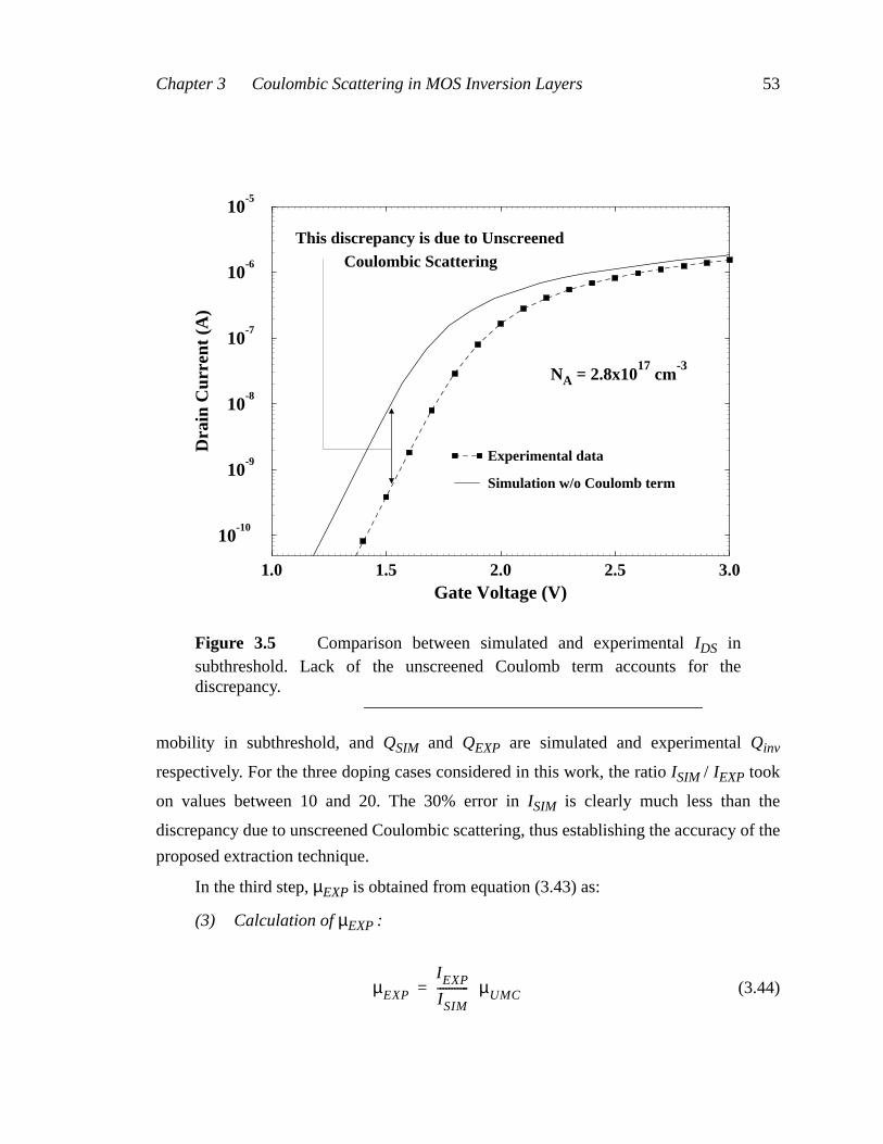
Chapter 3 Coulombic Scattering in MOS Inversion Layers 53
mobility in subthreshold, and QSIM and QEXP are simulated and experimental Qinv
respectively. For the three doping cases considered in this work, the ratio ISIM / IEXP took
on values between 10 and 20. The 30% error in ISIM is clearly much less than the
discrepancy due to unscreened Coulombic scattering, thus establishing the accuracy of the
proposed extraction technique.
In the third step, µEXP is obtained from equation (3.43) as:
(3) Calculation of µEXP :
(3.44)
1.0 1.5 2.0 2.5 3.0Gate Voltage (V)
10-10
10-9
10-8
10-7
10-6
10-5
Dra
in C
urre
nt (
A)
Experimental data
Simulation w/o Coulomb term
This discrepancy is due to Unscreened
NA = 2.8x10¹⁷
cm-3
Coulombic Scattering
Figure 3.5 Comparison between simulated and experimental IDS insubthreshold. Lack of the unscreened Coulomb term accounts for thediscrepancy.
µEXP
IEXP
ISIM----------- µUMC=

Chapter 3 Coulombic Scattering in MOS Inversion Layers 54
If we assume that the various scattering mechanisms can be summed up using
Matthiessen’s rule [14], then the unscreened Coulombic mobility µUN is calculated as:
(4) Calculation of µUN :
(3.45)
Thus, for each channel doping level, we are able to extract a value for unscreened
Coulombic mobility by performing steps 1 through 4. In the final step, we need to
calculate the effective substrate doping level associated with this mobility value.
It is important to note that besides affecting the calculation of Qinv , interfacial and
oxide charges also affect the calculation of Coulombic mobility. The total charge in
two-dimensions that would scatter inversion layer electrons is:
(3.46)
where Nif is the interfacial charge, Nf is the oxide charge, NA is the acceptor charge in the
channel and <Zinv> is the average thickness of the inversion layer in subthreshold. This
thickness is calculated from a self-consistent 1-D solution of the Schrodinger-Poisson’s
equation. Thus, the equivalent charge in the substrate <NA>eff that would scatter the
electrons is calculated as:
(5) Calculation of effective charge in substrate:
(3.47)
As can be seen from equation (3.47), the effect of interfacial and oxide charges is to
increase the “effective” channel doping density seen by the inversion layer electrons.
The result of applying steps 1 through 5 is shown in Fig. 3.6 which also presents the
comparison between extracted data, the new 2D model for unscreened Coulombic
scattering, and the 3D model of Conwell and Weisskopf [12]. As can be seen from Fig.
3.6, the new 2D model exhibits much better agreement than the 3D model, suggesting that
even in subthreshold, the electron gas behaves as a two-dimensional gas. This has to do
µUN
µUMC µEXP–
µUMCµEXP--------------------------------=
N2D Nif Nf NA Zinv⟨ ⟩⋅+ +=
NA⟨ ⟩eff
N2D
Zinv⟨ ⟩---------------≡
Nif Nf+
Zinv⟨ ⟩------------------ NA+=

Chapter 3 Coulombic Scattering in MOS Inversion Layers 55
with the fact that at high doping levels, such as those shown in Fig. 3.6, the potential wells
are still quite steep in subthreshold, leading to significant quantization of the electron gas.
3.6 Impact of Coulombic scattering on VT
Threshold voltage, VT , is a very important design parameter for digital MOS
applications since it represents the trade-off between Ioff , the off-state leakage, and Ion ,
the current drive of the MOSFET. Aggressive design and optimization of submicron
MOSFETs would require an accurate prediction of VT .
Consider the design of MOSFETs for low-power applications. One method for
Figure 3.6 Comparison between extracted experimental data, new 2Dmodel for unscreened Coulombic scattering, and 3D model due to Conwelland Weisskopf.
1016
1017
1018
Channel Doping (cm-3
)
101
102
103
104
105
106
Uns
cree
ned
Cou
lom
bic
Mob
ility
(cm
2 /V-s
ec)
Conwell-Weisskopf Model (3-D)
New First-Principles Model (2-D)
Experimental Data

Chapter 3 Coulombic Scattering in MOS Inversion Layers 56
reducing power dissipation, which is proportional to , is to scale Vdd. However,
reduction of Vdd causes Ion to decrease, which negatively impacts the performance of the
system. In an effort to improve the performance, the design of low-threshold devices has
been suggested [84], [4]. While the Ion of such devices would increase, so would Ioff
which would result in increased standby power dissipation. Thus, for devices that are to
operate at low Vdd , optimization of VT is required to maximize performance and minimize
standby power dissipation. If deep submicron MOSFETs are to be designed for low-power
applications using 2D device simulation tools, it is essential that the simulator be able to
accurately calculate the VT of such devices which are doped heavily to suppress
punchthrough and DIBL effects.
Figure 3.7 presents the VT comparison between experimental data and simulation
results obtained without a model for unscreened Coulombic scattering. The devices used
in this study have the same oxide thickness (250Å) but different channel doping levels.
Thus, as the channel doping is increased, the absolute value of threshold voltage also
increases. In practice, MOSFETs with heavily doped channels will have thinner oxides
(less than 250Å), as mandated by the scaling rules to keep the VT at a reasonable value.
What is important to note, however, is that the discrepancy between predicted and
measured VT values increases as the channel doping goes up. This is because there is
increased Coulombic scattering at higher channel doping levels, and hence the error is
expected to be larger. Therefore, it becomes even more important to include a model for
Coulombic scattering when designing MOSFETs with heavily doped channels. For
instance, 0.1µm MOSFETs are expected to have channel doping levels around 1x10¹⁸
cm-3 and would be designed to operate at a Vdd of 1.0 to 1.5V [6]. Thus, a mobility model
containing Coulombic scattering would be an important aid in technology scaling and
optimization.
3.7 Conclusion
In this chapter, a first-principles analysis of two dimensional Coulombic scattering
was presented. Unscreened Coulombic scattering was treated first, which is the scattering
of electrons by a bare Coulombic potential. This type of scattering dominates in weak
Vdd2

Chapter 3 Coulombic Scattering in MOS Inversion Layers 57
inversion where there are too few carriers to screen the Coulomb potential. To keep the
analysis tractable, the following assumptions were made: (a) the electron gas was treated
as being strictly two dimensional (i.e. the envelope wavefunction was taken to be a delta
function), and (b) the impurity atoms were assumed to be distributed as a sheet of charge
near the interface. The first assumption holds if there is strong quantization (i.e. the
deBroglie wavelength of electrons is larger than the confining potential). The second
assumption holds in deep submicron MOSFETs that tend to have a large amount of charge
implanted near the interface to suppress DIBL and punchthrough effects.
Screened Coulombic scattering was treated next. The longitudinal dielectric function
for the electron gas was calculated in the random phase approximation, which led to an
expression for the screened Coulomb potential. In addition to the assumptions made for
Figure 3.7 Comparison between experimental data and simulation resultsobtained without a model for unscreened Coulombic scattering.
1e+16 2e+17 4e+17 6e+17 8e+17 1e+18Channel Doping (cm-3 )
0.0
1.0
2.0
3.0
4.0
5.0T
hre
sho
ld V
olt
age
(V)
Experimental Data
Simulation results withoutCoulombic Mobility
TOX=250A

Chapter 3 Coulombic Scattering in MOS Inversion Layers 58
unscreened scattering, it was further assumed that for strongly screened scattering, the
single-particle relaxation time is approximately equal to the momentum relaxation time.
This assumption permitted a closed-form solution to be calculated for screened
Coulombic mobility. On comparison with experimental data, it was demonstrated that the
new 2D model for screened Coulombic scattering accurately captures the screening
dependence whereas the 3D model due to Brooks-Herring fails to do so. It was also
established that screened Coulombic mobility is a strong function of channel charge and
not of the effective electric field. This behavior is in sharp contrast with phonon and
surface roughness scattering.
Since no known technique exists for extracting unscreened Coulombic scattering, a
new and systematic technique was presented that involves quantum and classical
simulations and requires the use of C-V and I-V data. Comparison of the extracted data
with models showed that the new 2D model for unscreened Coulombic scattering gives
better agreement with experimental data than the 3D model based on the formulation of
Conwell and Weisskopf.
Finally, the importance of modeling Coulombic scattering in MOS inversion layers
was established by demonstrating its impact on critical design parameters such as
threshold voltage and off-state leakage current. It was noted that a mobility model
containing Coulombic scattering would be an important aid in technology scaling and
optimization.

59
Chapter 4
Numerical Modeling of theGeneralized Mobility curve
4.1 Introduction
To be able to better predict the I-V characteristics of modern scaled MOSFETs,
accurate mobility models are required which incorporate all of the basic scattering
mechanisms operating in the inversion layer. At least three different scattering
mechanisms have been identified that affect carrier mobility in the inversion layer. These
include phonon scattering, Coulomb scattering, and surface roughness scattering [72]. At
room temperature, Coulomb scattering is only important if there are a large number of
charge centers present which can arise from either interfacial charge or channel dopants.
Both phonon scattering and surface roughness scattering are important at room
temperature, with surface roughness being especially important at high transverse electric
fields. Therefore, in long channel MOSFETs with moderate to low channel doping levels,
inversion-layer mobility is primarily limited by phonon scattering and surface roughness
scattering.
There are two kinds of interactions possible between electrons and phonons: elastic
and inelastic scattering. In elastic scattering, the energy of the electron after collision with
the phonon is relatively unchanged, and this type of interaction dominates when the
electrons are not very energetic. In contrast, inelastic scattering involves energy exchange
between the electron and phonon systems, and the probability of this interaction increases
as the energy of the carriers increase.

Chapter 4 Numerical Modeling of the Generalized Mobility curve 60
In the ohmic regime, the relationship between carrier velocity v and longitudinal
electric field E is linear. In this regime, the applied fields are sufficiently low such that the
electron gas is always in thermodynamic equilibrium with the lattice, i.e. the temperature
of the electron gas is approximately equal to the lattice temperature. Thus, in the ohmic
regime, phonon scattering is predominantly elastic. However, as the magnitude of the
applied field increases, the electron gas is able to gain more energy from the field and
“heat” itself. The resulting hot carriers have a much higher probability of engaging in
inelastic collisions. In this regime, the relationship between velocity and applied field is no
longer linear. In the discussion that follows, we shall be concerned exclusively with
aspects of low-field transport in which . The constant of proportionality is termed as
mobility µ, and it is a measure of how well the carriers respond to a driving field E.
It is well known that low field mobility in a long channel MOSFET follows the
universal mobility curve [9], [33], [43], a concept that was first introduced by Sabnis and
Clemens [43]. The principal features of the universal mobility curve (UMC) are that it is
invariant to changes in (i) oxide thickness, (ii) channel doping, and (iii) substrate bias. The
universality of mobility indicates that it is a property associated with the Si/SiO2 system
and not a parameter sensitive to nominal process variations [43]. It was shown by Lee et.
al. [53] that the universal mobility curve can be explained on the basis of phonon
scattering and surface roughness scattering in the inversion layer.
In short channel MOSFETs, which tend to have high channel doping levels to
suppress punchthrough and drain-induced-barrier-lowering effects, another scattering
mechanism has become important, namely Coulombic scattering due to ionized channel
dopants. While phonon scattering and surface roughness scattering lead to the universal
mobility curve, it was experimentally observed by Takagi et. al. [9] that in the presence of
strong Coulombic scattering, marked deviations from the universal mobility curve are
obtained. The resulting curve is termed as the generalized mobility curve or the GMC.
In the previous chapter, we presented a theoretical analysis for two dimensional
Coulombic scattering in the inversion layer. The model presented there (see equations
(3.11), (3.35), and (3.36) ) was cast in terms of non-local variables such as Ninv and N2D ,
the electron and impurity charge density per unit of channel area respectively. While
physically based models may originally appear in non-local form, for implementation in
device simulators based on the finite-volume method [55] such as PISCES [54], it is
highly desirable to reformulate the model in terms of local variables such as n and N , the
v E∝

Chapter 4 Numerical Modeling of the Generalized Mobility curve 61
electron and impurity charge density per unit volume respectively.
Moment-based device simulators [55] solve a set of coupled non-linear partial
differential equations by discretizing them in space and time domain1. These discretized
equations are then solved by either linearizing or decoupling them [55], [56]. In the
discretization process, the continuum of space and time is broken into a set of discrete
points, which are typically called nodes. The goal then is to calculate the variables of
interest at these nodes at a given time. Thus, within a device simulator, a local
computation is one which involves information from the nearest neighboring nodes only.
The implication is that during the linearization step, the less the coupling among the
various nodes, the easier it is to solve the discretized set of algebraic equations. On the
other hand, a non local computation involves information from nodes that can be far apart.
This tends to increase the degree of coupling among the nodes in the device, whose
primary effect is to increase the computation time.
There are other attributes to implementing models in a local form. Parallel device
simulators that are based on the domain decomposition scheme [57] see a significant
decrease in computation speedup if non-local models are used. Moreover, local models
allow for the simulation of complex, non-planar 2-D and 3-D structures which is not
possible if a non-local formulation is used since a non-local model assumes a planar
structure [30].
In this chapter we present a local model for low-field mobility that includes phonon,
surface-roughness, and Coulombic scattering. A local model should satisfy the properties
attributed to the non-local generalized mobility curve (GMC), since the general form of
the GMC lends itself to physical interpretation [53]. We define the GMC as the sum of a
universal part (the Universal Mobility Curve (UMC) [43]) and a non-universal part [9].
The new model has been implemented in PISCES [54], a 2-D device simulator, and it
indeed reproduces the GMC over a wide range of parameters. Good agreement of the new
model with several sets of experimental data is shown.
The organization of this chapter is as follows. First, in Section 4.2, a physically
correct scheme is presented for combining the various scattering mechanisms. In Section
4.3, phonon scattering in MOSFETs is discussed: Section 4.3.2 presents the theoretical
1. The differential equations are converted into algebraic equations through the discretizationprocedure.

Chapter 4 Numerical Modeling of the Generalized Mobility curve 62
basis for 2D phonon scattering; Section 4.3.3 outlines the extraction of a 2D
semi-empirical model from the first-principles model; and Section 4.3.4 presents an
empirical model for 3D phonon scattering.
Surface roughness scattering is discussed next in Section 4.4: theoretical treatment is
considered in Section 4.4.1, and its semi-empirical formulation presented in Section 4.4.2.
Section 4.5 is concerned with Coulombic scattering. Since, a first-principles model
for 2D Coulombic scattering was presented in Chapter 3, Section 4.5.1 discusses the
extraction of the semi-empirical model. Section 4.5.2 presents an empirical model for 3D
Coulombic scattering.
The universal mobility curve is modeled in Section 4.6 by combining the
semi-empirical models for phonon and surface-roughness scattering. The parameters
appearing in phonon and surface-roughness terms are calibrated to reproduce all the
properties of the UMC.
Finally, in Section 4.7, the generalized mobility curve is modeled by including the
term for Coulombic scattering in the model for the UMC. The resulting semi-empirical
model is shown to accurately reproduce the GMC over a wide range of biases and channel
doping levels.
4.2 Formulation of the Model
Most formulations of inversion-layer mobility start with the following functional
form [29], [30], [31], [32]:
(4.1)
The surface term models the 2D scattering mechanisms, whereas the bulk term
models the 3D effects. Matthiessen’s rule summation is strictly correct when the scattering
mechanisms that are being added are independent [15], but not mutually exclusive.
Independence here means that the probability of scattering due to a particular mechanism
does not depend on the previous scattering events of a particle. Assumption of
independence allows us to simply add the momentum relaxation times to arrive at the total
relaxation time [15]. Moreover, if the energy-dependence of the scattering mechanisms
1µtotal------------- 1
µsurface------------------ 1
µbulk------------+=

Chapter 4 Numerical Modeling of the Generalized Mobility curve 63
are identical, then we can add the mobilities instead of relaxation times to arrive at the net
mobility [15]. This in essence is the Matthiessen’s summation rule.
The property of mutual-exclusiveness means that if a certain scattering event occurs,
then it precludes some other scattering event from happening. For example, in equation
(4.1), the phonon scattering term is added twice: first as a 2D term, and then as a 3D term.
However, calculation of mobility near the surface must only consider the interaction of a
quantized electron with a 3D phonon, and not the interaction of 3D electrons with 3D
phonons. Nevertheless, equation (4.1) includes both interactions, and thus is a limitation
of that formulation. We present a more physically-based formulation which is consistent
with the nature of the various scattering mechanisms involved. Instead of partitioning
events as either surface or bulk, we split them according to the nature of the perturbing
potential. Thus, the proposed formulation takes on the following form:
(4.2)
The hierarchical taxonomy of the new model in equation (4.2) is shown in Figure 4.1. A
detailed discussion on the modeling of each term in the hierarchy is covered in the
following sections.
4.3 Phonon Scattering
4.3.1 General Considerations
To ensure the mutual-exclusivity of phonon scattering, it is expressed as the infinity
norm1 of 2D phonon and 3D phonon scattering:
(4.3)
In this formulation, , the phonon-limited mobility near the surface, represents the
1. Lp norm of vector x is . Euclidean norm is p=2, whereas yields .
1µtotal------------- 1
µphonon------------------ 1
µsurface roughness---------------------------------------- 1
µCoulomb---------------------+ +=
xip
i∑p p ∞→ min xi: i=1,....,N
µph min µ2Dph µ3D
ph,=
µ2Dph

Chapter 4 Numerical Modeling of the Generalized Mobility curve 64
interaction between quantized electrons and bulk-mode (3D) phonons1, whereas , the
phonon-limited mobility in the bulk, represents the interaction between bulk electrons and
bulk-mode phonons. On the other hand, the physical interpretation of the commonly used
formulation — the one given in equation (4.1) — is that the calculation of phonon-limited
mobility near the surface considers the interaction of 2D electrons with 3D phonons (the
surface term) as well as the interaction of 3D electrons with 3D phonons (the bulk term).
Clearly, calculation of mobility near the surface in the presence of a strong transverse field
need not include the interaction of 3D electrons with phonons since electrons near the
surface are quantized! This distinction is elegantly handled by equations (4.2) and (4.3).
1. 3D phonons are generated by atomic vibrations in which the elastic constant of the lattice is closeto identical in all three directions, thus allowing bulk modes to exist. 2D phonons, also known assurfons, are generated if the elastic constant is sufficiently different in one direction, thus allowinginterface modes to exist. In the Si/SiO2 system, velocity of sound is not very different between thetwo media; hence, interface modes do not play a significant role in electron-phonon scattering.Thus, electron-phonon scattering in the inversion layer is treated entirely as the interactionbetween bulk-mode phonons and the two dimensional electron gas [8], [46].
Mobility
SurfaceRoughness CoulombPhonon
2D 3D 3D 2D2D
INV INV
Summation via Matthiessen’s Rule
Minimum Function 2D/3D Transition Function
Figure 4.1 Hierarchical taxonomy of the new semi-empirical local model.
INV
µ3Dph

Chapter 4 Numerical Modeling of the Generalized Mobility curve 65
Besides the fact that equation (4.1) inherently presents a non-physical picture, we shall see
later that such a formulation does not allow us to extend the model to accumulation layers.
Moreover, it was found that with the improved formulation given in equation (4.2),
calibrating parameters assumed values that were in closer agreement with first-principle
calculations.
4.3.2 Theoretical basis for 2D Phonon scattering
At room temperature, mobility in semiconductors is often dominated by phonon
scattering, and hence its study occupies a central place in the theory of electrical transport
in semiconductors. More importantly, phonon scattering unlike impurity scattering
provides a mechanism for energy loss, i.e. interaction of electrons with certain kinds of
phonons are inelastic in nature. In contrast, impurity scattering is purely elastic, and other
than contributing to momentum randomization, it plays no role in energy relaxation. For
instance, velocity saturation in semiconductors occurs entirely due to inelastic phonon
scattering.
In developing the theory of energy band structure, it is assumed that the lattice atoms
are frozen in space. However, in reality, the atoms vibrate about their equilibrium position,
and it is this vibration that accounts for the thermal energy of the lattice. As a result of
these vibrations, the periodic potential in the crystal varies with time and causes
alterations in the electronic states with time. The scattering of electrons due to alterations
in the periodic potential arising from atomic vibrations depends on the nature of these
vibrations and the nature of the atoms making up the crystal.
Atomic vibrations in the crystal generate elastic waves which can vibrate in one of
two modes. In the acoustic mode, neighboring atoms vibrate in phase, whereas in the
optical mode, they vibrate out of phase. The frequency of vibration, and hence the energy,
associated with the optical mode is higher than that of the acoustic mode. Optical mode
gets it name because electromagnetic radiation in the optical region of the spectrum
interacts with the optical mode, whereas acoustic mode gets it name because sound waves
in a solid propagate via the longitudinal1 acoustic mode. Phonons represent the
quasi-particles associated with vibratory motion in the crystal, and depending on the
1. It should be pointed out that both acoustic and optical modes can vibrate either transversely orlongitudinally.

Chapter 4 Numerical Modeling of the Generalized Mobility curve 66
mode, they are also termed as either acoustic or optical phonons.
Acoustic phonons in a crystal cause perturbations in potential in one of two ways.
First, due to changes in the spacing of the lattice atoms, the energy band gap and the
position of conduction and valence band edges vary from point to point. Potential
discontinuites are thus produced in the conduction and valence bands. The potential so
produced due to the deformation of the crystal is called the deformation potential, the
magnitude of which is evidently proportional to the strain produced by the vibrations. The
scattering of carriers by the deformation potential is called deformation potential
scattering. The second kind of perturbation is produced by acoustic vibrations through the
piezoelectric effect. If the atoms constituting the crystal are partially ionized, the
displacement of atoms due to the acoustic vibrations would produce potentials, the
magnitude of which would depend on the arrangement of the ionized atoms in the crystal.
The scattering of electrons by a piezoelectric potential is referred to as piezoelectric
scattering. This kind of scattering is important in compound semiconductors, particularly
at low temperatures.
Optical phonons also scatter electrons in one of two ways. The deformation of the
crystal due to optical vibrations produces a perturbing potential that is proportional to the
optical strain. This type of scattering is termed as deformation potential scattering via the
optical phonons, and in order to differentiate it from acoustic phonon deformation
potential scattering, it is typically termed as non-polar optical phonon scattering. The
second type of optical phonon scattering occurs by the creation of dipole moments due to
oppositely charged neighboring atoms. These dipole moments result in a perturbing
potential, and this type of scattering is known as polar optical phonon scattering.
Lastly, phonon scattering can either be intravalley or intervalley. The hierarchy of
lattice scattering is shown in Figure 4.2. In silicon with six equivalent X-valleys,
intervalley phonon scattering is an extremely important process, especially at high fields.
It should also be pointed out that acoustic phonon scattering is quasi-elastic since it
involves little exchange of energy with the electron. On the other hand, optical phonon
scattering is highly inelastic, and hence plays an important role in high-field transport.
In low field transport, acoustic phonon scattering plays an important role. In pure
silicon at low temperatures, intravalley acoustic phonon scattering dominates. As
temperature rises, intervalley scattering becomes important, while at room temperature
intravalley acoustic phonon scattering via the deformation potential and intervalley

Chapter 4 Numerical Modeling of the Generalized Mobility curve 67
scattering are equally frequent. While intravalley scattering is predominantly due to
acoustic phonon scattering, intervalley scattering is primarily due to optical phonon
scattering. Since, we are interested in deriving an expression for low field mobility, we
present a theoretical treatment of acoustic phonon scattering via the deformation potential
(ADP).
In the deformation potential interaction, the scattering between electrons and
phonons occurs when the electron waves scatter off phonon waves which are represented
by elastic waves in a solid [15]:
(4.4)
where u(x,t) is the atomic displacement from the equilibrium position, Aβ is the amplitude
of the wave, β is the wavevector, and ω is the frequency. Since atoms vibrate in phase in
acoustic phonon scattering, the interaction potential is given by [15]:
Lattice
Intervalley
Intravalley
Acoustic
Optical
DeformationPotential
Piezoelectric
DeformationPotential (non-polar)
Polar
Scattering
Acoustic
Optical
Figure 4.2 Hierarchical taxonomy of lattice scattering.
u x t,( ) Aβei βx ωt–+−( )
=

Chapter 4 Numerical Modeling of the Generalized Mobility curve 68
(4.5)
where Hac is the interaction potential, and Dac is known the deformation potential. The
matrix element can hence be written as:
(4.6)
By equating classical and quantum energy terms, the following expression for Aβ is
obtained [15]:
(4.7)
Nω is the occupation number of phonons (i.e. the number of phonons with frequency ω
and hence with energy ), M is the total mass of atoms that interact with the electrons,
Nω is specified by Bose-Einstein statistics, and in the equipartition approximation,
. From the dispersion relationship for phonons, , where ul is the
velocity of sound in the crystal. Thus, the square of the matrix element becomes:
(4.8)
In 3D, , where ρbulk is the density of silicon atoms per unit volume and V is
the volume. In 2D, , where ρarea is the density of silicon atoms per unit area
and Ω is the area. Since phonon scattering is isotropic (i.e. velocity randomizing),
momentum relaxation time is the same as the inverse of the total scattering rate [15] (also
see equation (2.27) ). The expression for the total scattering rate in two dimensions is
given by:
(4.9)
Hac Dac x∂∂u
i± βDacu= =
M k k ′,( ) i± DacAββ ei k k ′ β±–( ) x
xd∫ i± DacAββδ k k ′ β±–( )= =
Aβ2 Nω 1 2⁄+( ) h
2Mω---------------------------------=
hω
Nω kT hω⁄≈ ω β⁄ ul=
M k k ′,( ) 2 DackT
2ul2M
---------------δ k k ′ β±–( )=
M ρbulkV=
M ρareaΩ=
1τ ε( )------------
Ω
2π( ) 2--------------- 2π
h------ M k k ′,( ) 2δ ε ε′ h± ω+–( ) d
2k∫=

Chapter 4 Numerical Modeling of the Generalized Mobility curve 69
Substituting equation (4.8) in (4.9), the following expression for the momentum relaxation
time is obtained [58], [46], [63]:
(4.10)
Low-field mobility is obtained by averaging the momentum relaxation time weighted by
the energy over the distribution function [15], [59], [60]:
(4.11)
where fo(ε) is the Maxwell-Boltzmann distribution function, D(ε) is the density of states,
and ε is the energy. Substituting the momentum relaxation time given in equation (4.10)
into equation (4.11) yields the following expression for mobility [58], [47]:
(4.12)
Since ρarea is the areal mass density, it can be expressed as , where
Zinv is the thickness of the inversion layer. Hence, the expression for mobility takes on the
following form:
(4.13)
4.3.3 A Semi-Empirical Model for 2D Phonon scattering
Although the model appearing in equation (4.13) is calculated from first-principles,
it does not agree well with experimentally obtained results for phonon scattering in the
inversion layer. Due to the simplifying assumptions made in the derivation of the model in
equation (4.13), a good agreement is not expected in the first place. However, what
1τac-------
m∗ Dac2
kT
h3ρareaul
2------------------------=
µ qm∗------- 2
3kT---------
ε τ ε( ) fo ε( ) D ε( )⋅⋅⋅ εd∫fo ε( ) D ε( ) εd⋅∫
-----------------------------------------------------------------=
µac2D qh
2ρareaul
2
m∗( )2Dac
2kT
--------------------------------=
ρarea ρbulk Zinv⋅=
µac2D qh
2ρbulkul
2
m∗( )2Dac
2k
----------------------------- 1T--- Z⋅
inv⋅=

Chapter 4 Numerical Modeling of the Generalized Mobility curve 70
equation (4.13) does provide is an insight into the trend of how acoustic phonon mobility
changes with respect to parameters such as temperature and inversion-layer thickness. In
formulating a model that must agree with experimental data, the functional dependences
from the first-principles model in equation (4.13) are retained but the proportionality
constant is allowed to vary to achieve good agreement with experimental data. Such an
approach is termed as semi-empirical modeling since we start with a physically-based
formulation, but vary prefactorial parameters until a good match with experimental data is
obtained. At the other extreme is empirical modeling in which all the parameters are
allowed to vary. Therefore, when equation (4.13) is cast in semi-empirical form, the
following expression is obtained [30]:
(4.14)
where Λ is a calibrating parameter to be determined by comparison with experimental
data, T is the lattice temperature, and Zinv is the thickness (or the width) of the quasi-two-
dimensional1 electron gas. The width of the inversion layer can be calculated either
classically or quantum mechanically.
A quantum mechanical analysis, in which the wave nature of electrons is
emphasized, is necessary if the dimension of the confining potential is comparable to the
deBroglie wavelength, , of electrons, which at room temperature is
approximately 150Å. In modern submicrometer MOSFETs, thinner gate oxides have
resulted in steeper potential wells near the interface, thus mandating a partial if not a
complete quantum mechanical treatment. If the electrons are indeed represented as
wavefunctions, then it has been found that the nature of the electron distribution in the
channel is significantly different from the case in which the electrons are treated as
classical particles [48], [49]. Figure 4.3 illustrates this difference. The potential at the Si/
SiO2 interface is assumed to be infinitely large. Hence the wavefunction vanishes at the
interface because of which the probability of finding an electron at the interface is zero.
Contrast this with the classical calculation in which the electron density is maximum at the
interface.
1. Quasi-2D instead of strictly 2D because of the finite spatial extent in the depth direction. It is thisspatial extent that we are defining as the width of the inversion layer.
µ2Dphonon Λ 1
T--- Zinv⋅ ⋅=
λel h 3m∗ kBT⁄=

Chapter 4 Numerical Modeling of the Generalized Mobility curve 71
In the quantum mechanical calculation, Poisson and Schrodinger equation is solved
self-consistently. For Poisson equation, the input is the charge density, and the output is
the potential profile which forms the input to Schrodinger equation whose output is the
wavefunction ψ(z) and the energy eigen-values εi . Thus, the coupling between the two
equations is via a constitutive equation relating the wavefunction to the electron density. If
the number of electrons in a particular subband is Ni , then the electron density at a point z
below the interface is:
(4.15)
where is the wavefunction in the i-th subband. Ni can be simply calculated through
the 2D density of states and the Fermi-Dirac distribution function:
(4.16)
quantum mechanicaldistribution
classical distributionE
lect
ron
Con
cent
ratio
n
Distance from Si/SiO2 interface
Figure 4.3 Comparison between classical and quantum mechanical calculations ofelectron density in the inversion layer of MOSFETs.
n z( ) Ni ψi z( ) 2⋅i
∑=
ψi z( )
Ni
gvmd
πh2
------------ f ε( ) εd
εi
∞
∫gvmd
πh2
------------kT 1 eεF εi–( ) kT( )⁄
+ln= =

Chapter 4 Numerical Modeling of the Generalized Mobility curve 72
where gv is the valley degeneracy, md is the density-of-states effective mass, εi is the
energy eigenvalue in the i-th band, and εF is the fermi level.
The primary difference between the quantum calculation and the classical
calculation is that in the classical calculation, Schrodinger equation is not solved for.
Instead the electron density is given by the usual 3D calculation:
(4.17)
To compute the quantum mechanical thickness of the electron gas, we start by
computing the average thickness of the electron gas in each subband [44]:
(4.18)
The average thickness for the quantized gas is then given by averaging over all the <zi>:
(4.19)
where ci is the fraction of the total number of electrons in the i-th subband:
(4.20)
Calculating ZQM via equations (4.18) and (4.19) requires knowing first,
which can only be obtained by numerically solving Schrodinger’s equation and Poisson’s
equation in a self-consistent fashion. However, if we seek an analytical solution, the two
equations can be decoupled by assuming some reasonable form for the potential profile in
the inversion layer. The assumption typically made is that of a triangular well and the
resulting wavefunctions are given by Airy functions [49]. However, Stern [45] points out
that the triangular well approximation is a reasonable one if there is little or no charge in
the inversion layer, but it fails if the inversion-layer charge is comparable to or more than
the depletion layer charge. When only one subband is occupied (i.e. in the electric
n z( ) D ε( ) f ε( ) εd
εC z( )
∞
∫ NCeεF εC z( )–[ ] kT( )⁄
≈=
zi⟨ ⟩ ψ i∗ r z,( ) z ψi r z,( )⋅ ⋅ zd rd∫ ψi
∗ z( ) z ψi z( )⋅ ⋅ zd∫= =
ZQM ci zi⟨ ⟩i
∑=
ci
Ni
Nii
∑------------=
ψi z( )
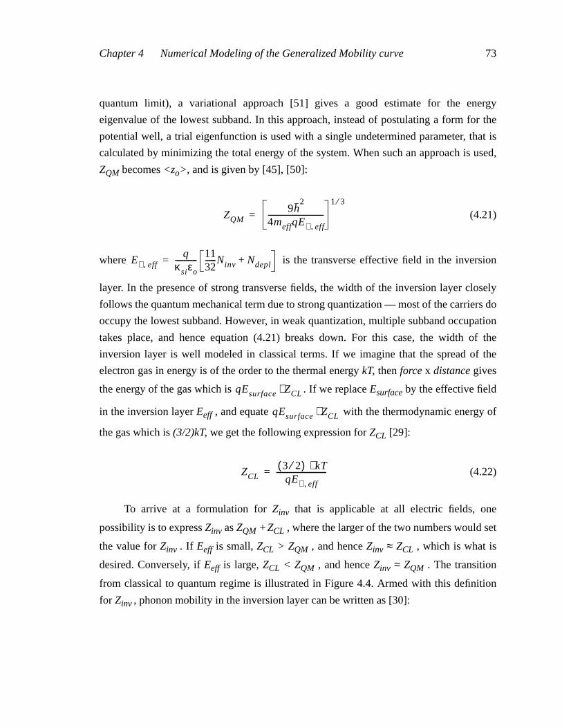
Chapter 4 Numerical Modeling of the Generalized Mobility curve 73
quantum limit), a variational approach [51] gives a good estimate for the energy
eigenvalue of the lowest subband. In this approach, instead of postulating a form for the
potential well, a trial eigenfunction is used with a single undetermined parameter, that is
calculated by minimizing the total energy of the system. When such an approach is used,
ZQM becomes <zo>, and is given by [45], [50]:
(4.21)
where is the transverse effective field in the inversion
layer. In the presence of strong transverse fields, the width of the inversion layer closely
follows the quantum mechanical term due to strong quantization — most of the carriers do
occupy the lowest subband. However, in weak quantization, multiple subband occupation
takes place, and hence equation (4.21) breaks down. For this case, the width of the
inversion layer is well modeled in classical terms. If we imagine that the spread of the
electron gas in energy is of the order to the thermal energy kT, then force x distance gives
the energy of the gas which is . If we replace Esurface by the effective field
in the inversion layer Eeff , and equate with the thermodynamic energy of
the gas which is (3/2)kT, we get the following expression for ZCL [29]:
(4.22)
To arrive at a formulation for Zinv that is applicable at all electric fields, one
possibility is to express Zinv as ZQM +ZCL , where the larger of the two numbers would set
the value for Zinv . If Eeff is small, ZCL > ZQM , and hence Zinv ≈ ZCL , which is what is
desired. Conversely, if Eeff is large, ZCL < ZQM , and hence Zinv ≈ ZQM . The transition
from classical to quantum regime is illustrated in Figure 4.4. Armed with this definition
for Zinv , phonon mobility in the inversion layer can be written as [30]:
ZQM9h
2
4meffqE⊥ eff,------------------------------
1 3⁄
=
E⊥ eff,q
κ siεo------------ 11
32------Ninv Ndepl+=
qEsurface ZCL⋅
qEsurface ZCL⋅
ZCL3 2⁄( ) kT⋅qE⊥ eff,
---------------------------=

Chapter 4 Numerical Modeling of the Generalized Mobility curve 74
(4.23)
The effective field appearing in equation (4.23) is a non-local quantity, i.e. its calculation
requires summing information from various nodes. From a numerical simulation point of
view, non-local quantities are highly undesirable since they potentially slow down the
computation by increasing the bandwidth of the Jacobian matrix [55]. On the other hand,
if the Jacobian entries are altogether neglected, then it is not possible to perform an
accurate small signal analysis using the model [1]. Finally, it is implicit in the definition of
the non-local field that it assumes planarity of the Si/SiO2 interface which limits the
simulation to planar devices only [1].
On the other hand, the definition of the local electric field is based on local
information only. It allows the Jacobian to be set up symbolically for small signal analysis;
does not increase the bandwidth of the Jacobian matrix, and allows for the simulation of
non-planar devices. Thus, from a numerical implementation point of view, all models
should be strictly locally based [1]. By their very nature, macroscopic models derived
from basic physics would necessarily involve averaging over microscopic quantities. In
certain instances, such as for the two dimensional electron gas, averaging would be
Log(Eeff)
Zinversion
slope ~ 1/3
slope ~ 1
Figure 4.4 Thickness of the inversion layer as a function of transverse electric field.At low fields, classical formulation is required, whereas at high fields, quantummechanical formulation is applicable.
µinvph A
E⊥ eff,--------------
B NγA⋅
T E⊥ eff,1 3⁄⋅
---------------------+=

Chapter 4 Numerical Modeling of the Generalized Mobility curve 75
performed spatially as well, resulting in a reduced-dimensionality variable such as
integrated channel charge Ninv . For such cases, we need to make the transformation at the
numerical level from a 2D variable to a 3D variable.
In going from a 3D to a 2D variable, integration needs to be performed over one of
the space coordinates. For instance, in the case of the non-local effective field
(4.24)
where is the local transverse electric field at coordinate z below the Si/SiO2
interface, and n(z) is the local electron concentration at z. While there is a unique
transformation from to Eeff , the reverse transformation is clearly not unique. One
possibility is to simply set Eeff equal to as proposed by Lombardi et. al. [30]. Although
this may appear to be an ad hoc approach, it should be noticed that the formulation in
equation (4.14) is a semi-empirical approach to begin with, and hence any further
deviation between theory and experiment due to such a transformation can be easily
accommodated by recalibrating the fitting parameter Λ. Thus, the resulting semi-empirical
model for phonon scattering in the inversion layer is given by:
(4.25)
Ideally, the fitting parameter γ appearing in equation (4.25) should be zero, since
electron-phonon interactions depend on the vibrational properties of the lattice and not
specifically the dopant concentration. The need for a non-zero γ can be postulated as
follows. Note that the model in equation (4.25) is formulated as a local model (i.e. is a
local function of the space coordinates (x,y,z) ). On the other hand, the experimentally
observed universal mobility curve [43] is expressed as a function of the non-local
transverse electric field Eeff defined in equation (4.24). The calculation of a non-local
mobility from the local mobility involves integration in the depth direction (similar to the
case of the non-local electric field):
E⊥ eff,E⊥ z( ) n z( ) zd∫
n z( ) zd∫--------------------------------------=
E⊥ z( )
E⊥
E⊥
µinvph
r( ) AE⊥ r( )----------------
B NγA⋅
T E⊥1 3⁄
r( )⋅----------------------------+=
E⊥

Chapter 4 Numerical Modeling of the Generalized Mobility curve 76
(4.26)
The effective mobility obtained via equation (4.26) needs to reproduce the universal
mobility curve [43], and it was observed that a slight dependence of NA is required in
equation (4.25) in order to fit the local model with experimental data. This may have to do
with the fact that since there is no unique transformation from the non-local field to the
local electric field, making the arbitrary transformation of in equation (4.25)
introduces a functional dependence on NA .
4.3.4 An Empirical Model for 3D Phonon Scattering
Scattering rate due to any perturbing potential is proportional to the density of states
available to the particles [64]. Confinement changes the energy dependence of the electron
density of states in a parabolic band structure from ε1/2 in the bulk to εo in 2D. Thus, for
three dimensional scattering, the momentum relaxation time obtained in equation (4.10)
for two dimensions changes to:
(4.27)
From equation (4.11), mobility for 3D phonons is thus calculated to be:
(4.28)
In comparing 3D mobility with 2D mobility (see equation (4.12)), we see that the
temperature dependence is much stronger in 3D compared to 2D. While equation (4.28)
provides a first-principles model, it is found experimentally that phonon mobility does not
quite follow the T -1.5 dependence as given in (4.28). Instead, the dependence is found to
be stronger, and hence the model for phonon scattering becomes purely empirical since we
calibrate both the proportionality constant as well as the exponent. Recall that in a
µeff
µ z( ) n z( ) zd∫n z( ) zd∫
----------------------------------=
Eeff E⊥→
1τac-------
πDac2
kT
hρbulkul2
---------------------g3D ε( )DackT 2m∗( )
3 2⁄ε1 2⁄
4πh4ρbulkul
2----------------------------------------------------= =
µac3D 2
2 3⁄
3----------
qπ1 2⁄h
4ρbulkul
2
Dac2
m∗( )5 2⁄
kT( ) 3 2⁄----------------------------------------------------=

Chapter 4 Numerical Modeling of the Generalized Mobility curve 77
semi-empirical model, the exponent is taken straight from first-principles analysis. Thus,
the model for three dimensional phonon scattering takes the form [61], [62]:
(4.29)
where θ = 2.285 and µmax = 1417 cm2/V-sec. Therefore, the expression for total phonon
mobility given by equation (4.3) becomes:
(4.30)
In equation (4.30), the parameter that determines whether phonon mobility is given
by the 2D term or by the 3D term is the transverse electric field . If gate bias is
sufficiently large to cause inversion and hence quantization of the electron gas, then
is large near the interface. Thus, the calculation of , which is inversely related
to , would result in a small numerical value. If this value is less than the value for
, then would be given by . In going from the surface into the bulk,
decreases in value, and hence increases in value. If exceeds , then at that
point, is given by . The transition from 2D to 3D mobility is illustrated in Figure
4.5.
4.4 Surface Roughness Scattering
In deep submicron MOSFETs with scaled dielectrics, surface roughness scattering
has become a major limiting factor due to the presence of high transverse electric fields.
We first present a first principles approach to modeling surface roughness, and then
present a semi-empirical model that is calibrated against experimental data.
µac3D µmax
300T
--------- θ
=
µph min AE⊥ r( )----------------
B NγA⋅
T E⊥1 3⁄
r( )⋅----------------------------+ µmax
300T
--------- θ
,=
E⊥ r( )
E⊥ r( ) µph2D
E⊥ r( )
µph3D µph µph
2DE⊥ r( )
µph2D µph
2D µph3D
µph µph3D

Chapter 4 Numerical Modeling of the Generalized Mobility curve 78
4.4.1 Theoretical basis for Surface Roughness Scattering
Surface roughness occurs due to surface irregularities at the interface. Thus, it is
purely a two dimensional effect with no analog in the bulk. Surface roughness scattering
has been theoretically investigated using a simple model [65] which assumes that only the
lowest subbands are occupied, and deviations from perfect planarity ∆(x,y) are small in
magnitude and slowly varying in the x-y plane. Here we assume that the x-y plane is
parallel to the Si/SiO2 interface.
Due to variations in the z direction, i.e. the direction normal to the interface,
potential in the z direction is perturbed as well. Hence, the resulting Hamiltonian is given
by [66]:
Gate Oxide Silicon Substrate
Distance
Phon
on M
obili
ty
2D term
3D term
Figure 4.5 Illustrating the transition from 2D mobility to 3D mobility as one movesfrom the surface into the bulk. The assumption in this figure is that there is sufficientgate bias to cause the 2D term at the interface to be less than the 3D term (which isindependent of the value of transverse electric field).

Chapter 4 Numerical Modeling of the Generalized Mobility curve 79
(4.31)
Thus, the perturbing (interaction) potential, H-Ho, is given by:
(4.32)
Therefore, the matrix element for this perturbing potential is given by [67]:
(4.33)
To evaluate the first integral on the right hand side, the variational wavefunction ζ(z)
proposed by Stern and Howard [50] is used:
(4.34)
where
(4.35)
As shown by Matsumoto and Uemura [68], the integral is proportional to the effective
field in the inversion layer:
(4.36)
The second integral on the right hand side of equation (4.33) is simply the spatial Fourier
transform of ∆(x,y):
H Ho δH+h
2
2m------- ∇ 2
– V z ∆ x y,( )+[ ]+= =
δH V z ∆ x y,( )–[ ] V z[ ]z∂
∂V∆ x y,( )≈–=
Ψ′⟨ |δH Ψ| ⟩ ζ∗ z( )z∂
∂Vζ z( ) zd
∞–
∞
∫ 1A---× ∆ R( ) e
i k k–( ) R⋅Rd
A∫=
ζ z( ) b3
2-----ze
bz 2⁄–=
b48πe
2m
κsih2
------------------- Ndepl1132------Ninv+⋅
3=
ζ∗ z( )z∂
∂Vζ z( ) zd
∞–
∞
∫ q2
κsiεo------------ 11
32------Ninv Ndepl+
qEeff= =

Chapter 4 Numerical Modeling of the Generalized Mobility curve 80
(4.37)
where . ∆(R) is assumed to have a Gaussian form of correlation between two
points [69] such that:
(4.38)
where <⋅ ⋅ ⋅> denotes the sample average, ∆ is the root mean square deviation of the
interface, and Λ is the correlation length. Defined this way, is obtained as [67]:
(4.39)
If we neglect screening by the 2D electron gas, then the square of the matrix element is
given by:
(4.40)
and hence the scattering probability via the Fermi’s Golden Rule is obtained as:
(4.41)
The momentum relaxation time for an elastic scattering event such as Coulombic
scattering or surface roughness scattering is given by equation (2.35):
(4.42)
Therefore, the momentum relaxation time for surface roughness scattering is given by:
(4.43)
∆ q( ) 1A--- ∆ R( ) e
i k k'–( ) R⋅Rd
A∫=
q k k ′–=
∆ R( ) ∆ R R1+( )⟨ ⟩ ∆ 2e
R12 Λ2⁄–
=
∆ q( ) 2
∆ q( ) 2 π∆2Λ2
A----------------e
q–2Λ2
4⁄=
Ψ′⟨ |δH Ψ| ⟩ 2q
2Eeff
2 ∆ q( ) 2=
S k k ′,( ) 2πh
------ Ψ′⟨ |δH Ψ| ⟩ 2δ ε k( ) ε k ′( )–[ ] 2πh
------q2Eeff
2 ∆ q( ) 2δ εk εk ′–( )= =
1τm k( )----------------
A
2π( ) 2--------------- S k k ′,( ) 1 θcos–[ ] k ′d∫=
1τsr------
q2Eeff
2 ∆2Λ2
2h---------------------------- e
q–2Λ2
4⁄ δ εk εk ′–( ) 1 θcos–[ ] k ′d∫=

Chapter 4 Numerical Modeling of the Generalized Mobility curve 81
As shown by Harstein et. al. [52], the correlation length Λ is about 6Å, and hence the
quantity kΛ is much less than unity. In this case, the relaxation time for surface roughness
is approximated by:
(4.44)
and the corresponding mobility calculated from equation (4.11) is obtained as:
(4.45)
Thus, we find that surface roughness mobility has a much stronger dependence on the
transverse effective field compared to phonon mobility. That is why at high electric fields,
mobility is limited more by surface roughness scattering than by phonon scattering.
4.4.2 A Semi-Empirical Model for Surface Roughness Scattering
The first principles model for surface roughness scattering is presented in equation
(4.45). In some sense, it is a semi-empirical model since the parameters ∆ and Λ that
characterize the Si/SiO2 interface cannot be obtained from a microscopic description of
the interface since such a calculation does not exist at present. Instead, ∆ and Λ are
typically determined by fitting experimental data with the model in equation (4.45). If we
lump all the parameters and constants into one fitting parameter, the resulting
semi-empirical model becomes [52]:
(4.46)
In transforming the model from a non-local formulation to a local formulation, we set Eeff
as to obtain [1], [30]:
1τsr------
πm∗ ∆ΛqEeff( ) 2
h3
-----------------------------------------=
µsrh
3
π m∗( )2
∆Λ( ) 2q
----------------------------------------- 1
Eeff2
--------⋅=
µsrδ
Eeff2
--------=
E⊥
Chapter 4 Numerical Modeling of the Generalized Mobility curve 82
(4.47)
When the universal mobility curve was extracted using equations (4.24) and (4.26)
from the local model as defined later in equation (4.80), it was found that a constant δfailed to reproduce the experimental UMC. As for the case of phonon scattering (see
equation (4.25)), incorporating a slight doping dependence in the δ term led to good
agreement between the local model and experimental results. Thus, the resulting model
for surface roughness scattering is postulated as:
(4.48)
Note that surface roughness scattering is really a 2D scattering mechanism with no
analog in 3D. Thus, as the distance from the surface increases, the magnitude of the
transverse electric field decreases, and surface roughness mobility increases. The
transverse electric field approaches zero in the bulk region; hence surface roughness
mobility tends to infinity. Thus, the surface roughness term drops out in the calculation of
total mobility as given by the Matthiessen’s summation in equation (4.2).
4.5 Coulombic Scattering
Having discussed the semi-empirical formulations for phonon and surface roughness
scattering, we now turn our attention to Coulombic scattering. In semiconductors,
Coulombic scattering is the interaction of carriers (electron or holes) with any form of
charge centers. These charge centers can be either stationary such as ionized impurity
atoms, interfacial charges at the Si-SiO2 interface, fixed charges in the oxide or they may
be mobile such as carriers themselves. Coulombic scattering between carriers and
stationary centers can be treated within the framework of one formulation, whereas
carrier-carrier scattering requires a separate formulation since now the scattering potential
is no longer constant as is the case for the scattering of carriers by stationary centers. In
what follows, we are primarily interested in Coulombic scattering due to ionized
impurities, which is also simply known as impurity scattering. Note that the terms
µsrδ
E⊥2
r( )----------------=
µsr
C NAγ⋅
E⊥2
r( )----------------=

Chapter 4 Numerical Modeling of the Generalized Mobility curve 83
Coulombic scattering and impurity scattering would be used interchangeably since only
one mechanism in the hierarchy of Coulombic scattering is being considered.
Coulombic scattering requires a slightly different formulation from phonon
scattering since in the case of Coulombic scattering there is no natural variable that allows
a transition to be made from 2D to 3D mobility. In the case of phonon scattering (see
equation (4.30) ), the transverse electric field serves the role of a transition variable,
and such a formulation works very well since 2D phonon mobility is a function of (see
equation (4.25)) whereas 3D phonon mobility is independent of (see equation (4.29)).
The problem arises because of the fact that inherently, Coulombic scattering in 2D is
a function of the electron density, and not of the electric field. In other words, changes in
Eeff do not necessarily cause changes in Coulombic mobility unless carrier density
changes as well. This is due to the fact that Eeff can change while Ninv is held constant.
This is seen most simply by examining the relationship between Eeff and Ninv:
(4.49)
While , it can be easily shown that .
Thus combinations of Vgs and Vsb that keep Ninv constant would not hold Eeff constant and
vice versa. The lack of a one-to-one correspondence between Eeff and Ninv is evident from
equation (4.49) where it can be seen that a monotonically changing Ninv does not
guarantee a monotonically changing Eeff . The lack of a unique relationship between Ninv
and Eeff is why the Ninv dependence in Coulombic scattering cannot be transformed to an
Eeff dependence.
For phonon scattering, the field term serves as a useful transition variable
since 2D phonon mobility varies with but 3D phonon mobility does not. However,
for Coulombic scattering, the electron density n(r) cannot be directly used as a transition
variable either since both 2D and 3D Coulombic mobilities are functions of n(r). Since
neither of the intrinsic variables n(r) or can be used as transition variables,
transition functions are explicitly created that delineate the two and three dimensional
E⊥
E⊥
E⊥
Eeffqεsi------ ηNinv Ndepl+[ ]=
Ninv Vgs VT Vsb( )–[ ]∝ Eeff Vgs VT Vsb( )+[ ]∝
E⊥ r( )
E⊥ r( )
E⊥ r( )

Chapter 4 Numerical Modeling of the Generalized Mobility curve 84
regimes.
The most natural way to distinguish between 2D and 3D regimes is to consider the
nature of a quantum well (i.e. the degree of quantization). A steep potential well would
indicate strong quantization, and hence a two dimensional behavior, whereas a shallow
potential well would indicate weak quantization, and thus warrant a three dimensional
treatment.
To formulate the transition function for Coulombic scattering, it is postulated that in
a narrow quantum well the electron gas is quantized, and Coulombic mobility is given by
the 2D term. On the other hand, in a shallow quantum well the electron gas behaves like a
3D gas, and hence Coulombic mobility is given by the 3D term. In the triangular well
approximation [8], the energy eigenvalue of the i-th sub-band is given by:
(4.50)
Figure 4.6 illustrates the formation of subbands in the quasi-triangular potential well. Note
εi3πh
2----------
2 3⁄q
2 3⁄ 12mz---------
1 3⁄i 0.75+( ) 2 3⁄
E⊥ eff,2 3⁄⋅ ⋅ ⋅ ⋅=
Oxide Silicon Substrate
εo
ε1
ε2conduction band
Bulk-like2D-like
2D-like
Bulk-like
Figure 4.6 Illustrating the formation of energy subbands due to triangular wellconfinement of the electron gas near the Si-SiO2 interface.

Chapter 4 Numerical Modeling of the Generalized Mobility curve 85
that in going from the surface into the bulk, the confinement length between the
conduction band and the oxide barrier increases, thus reducing the degree of quantization.
Since quantization is strongest near the bottom of the conduction band, the separation of
sub-bands is largest near the bottom which decreases as one moves towards the bulk.
Therefore, the energy separation between the lower subbands can serve as a good
indicator for the degree of quantization. Considering just the energy separation between
the zeroth and the first energy level, one obtains from equation (4.50):
(4.51)
The transformation is made in order to allow for a local calculation.
If the Si-SiO2 interface is along the (100) plane, two sets of energy sub-bands, also
known as ladders, are created in the quantum well due to differing effective masses. From
the six-fold degeneracy of the silicon band structure, two valleys are aligned with the
transverse field, whereas the other four valleys are perpendicular to the transverse field.
Electrons in the aligned valleys exhibit longitudinal mass, whereas those in the
perpendicular valleys exhibit transverse mass. In silicon, the transverse effective mass is
smaller, and from equation (4.51) this set of energy bands exhibits greater sub-band
separation. On the other hand, the two valleys with the longitudinal mass are less
separated in energy, and in absolute values also are lower in energy. For instance, energy
of the lowest sub-band in the longitudinal ladder set is lower than that of the transverse
set. Thus, the longitudinal ladder set is considered in our calculations since it is the first to
get occupied. For this ladder, meff = 0.92, and hence, equation (4.51) becomes:
(4.52)
where E⊥ is expressed in V/m and ∆ε in Joules.
If the energy separation, , is larger than kT, the thermal spreading energy, then
most of the carriers would occupy the ground state, and the electron gas can be treated as
being quantized or two-dimensional. Conversely, if the energy separation is smaller than
kT, then both the sub-bands would be occupied, and we can treat the electron gas as being
ε1 ε0– ∆ε 9.4926–×10
E⊥ eff,2
meff--------------
1 3⁄
⋅= =
E⊥ eff, E⊥ r( )→
ε1 ε0– ∆ε 9.75726–×10 E⊥
2 3⁄r( )⋅= =
∆ε

Chapter 4 Numerical Modeling of the Generalized Mobility curve 86
bulk-like. Thus, the parameter of interest, α, is defined as :
(4.53)
where E⊥ is expressed in V/cm, k is the Boltzmann’s constant, and T is the temperature in
Kelvins.
If α is large, the quantization is strong, and conversely, for small α electrons behave
like a 3D gas. A transformation is required from α to a number which is bounded between
zero and one. For instance, when α is large, this function of α should map to zero, and if αis small, it should map to one. Clearly a threshold point is needed and also a specification
of the degree of abruptness of the transition from zero to one. One possible transform
function, closely resembling the Fermi-Dirac distribution function, is proposed below:
(4.54)
The transition point is defined by λ (akin to the fermi level), and the abruptness of the
transition is defined by η (akin to kT). Postulating that if ∆ε > 2kT, the electron gas near
the surface is quantized, and conversely if ∆ε < 2kT, it is bulk-like, λ is set equal to 2. In
order to make the transition from 2D to 3D sharp, η is chosen to be 0.5. The function f (α)
is schematically shown in Figure 4.7. Thus, Coulombic mobility can now be expressed as:
(4.55)
Near the interface if is large, would be large, and consequently α would be large.
Hence, f(α) would be close to zero, and the Coulombic mobility in equation (4.55) would
tend to . Conversely, if at any point in the device the transverse field (also
called the confining field) is small, α would be small and f(α) would be close to one. The
resulting Coulombic mobility would then be equal to .
∆ε kT⁄
α2.1
24–×10 E⊥2 3⁄⋅
kT---------------------------------------=
f α( ) 1
1 eα λ–( ) η⁄
+--------------------------------=
µcoulomb f α( ) µ3Dcoulomb
1 f α( )–[ ] µ 2Dcoulomb⋅+⋅=
E⊥ ∆ε
µ2Dcoulomb
E⊥
µ3Dcoulomb

Chapter 4 Numerical Modeling of the Generalized Mobility curve 87
4.5.1 A Semi-Empirical Model for 2D Coulombic Scattering
In Chapter 3, a first principles model for two dimensional Coulombic scattering was
presented [2], which is a non-local model since it is a function of the integrated channel
charge, Ninv that is obtained from the local electron concentration by integration:
(4.56)
where x is the direction from the source to the drain and z is the direction from the
interface into the bulk. To arrive at a local formulation for 2D Coulombic scattering, the
transformation is made, and all proportionality constants appearing in the
first-principles model are replaced with calibrating parameters. For Coulombic scattering,
it is found that to get the best fits, the exponents need to be perturbed as well, thus
resulting in the following model [1]:
(4.57)
Figure 4.7 The transition function f(α) from 2D to 3D Coulombic mobility.
α = ∆ε/kΤλ
slope ∝ 1/η
f(α) 3D regime
2D regime
1
0
Ninv x( ) n x z,( ) zd
0
∞
∫=
Ninv n→
µcoul2D
max D1n
κ
NA
β1-----------
D2
NA
β2-----------
,=

Chapter 4 Numerical Modeling of the Generalized Mobility curve 88
where n is the local electron concentration and NA is background acceptor atoms density.
The first term represents the screened and the second term represents the unscreened
Coulombic scattering. As electron density in the inversion-layer increases, the free charge
carriers screen out the Coulomb field due to the acceptor atoms, and hence, the mobility
increases. Conversely, as the free carrier concentration asymptotically goes to zero,
mobility due to the screened term also goes to zero. However, physically, as the electron
concentration decreases, mobility saturates at a constant value which is determined by
unscreened mobility. Note that the second term in equation (4.57) is independent of n and
is a function of NA only.
4.5.2 An Empirical Model for 3D Coulombic Scattering
For three dimensional Coulombic scattering, i.e. Coulombic scattering in the bulk,
the model presented by Klaassen [34] is used. There are two types of Coulombic
scattering that can occur in the bulk. Majority impurity scattering is the scattering of
majority carriers by background dopants such as the scattering of electron by donors or of
holes by acceptors. On the other hand, minority impurity scattering is that of minority
carriers by dopant atoms. This for instance would include cases such as the scattering of
electrons by acceptor atoms or the scattering of holes by donor atoms. Similarly, there are
two types of Coulombic scattering in 2D. In the previous section Coulombic scattering in
the inversion layer was discussed, which can also be considered as minority impurity
scattering. In the next chapter, 2D Coulombic scattering in MOS accumulation layer (such
as those that occur in the LDD regions of MOSFETs) would be considered and a model
presented for majority impurity scattering in 2D.
The case most often treated in bulk is majority impurity scattering, since majority
carriers are supplied by the background dopant atoms. Minority carrier scattering in 3D
only becomes significant in situations that involve carrier injection, such as in the base of
a bipolar transistor or in a p-n junction diode. Moreover, the models typically quoted for
3D majority impurity scattering also tacitly assume that the majority carrier concentration
is equal to the density of the background dopants. While such an assumption is reasonable
for majority carriers, the concentration of minority carriers is set by the degree of injection
(or inversion in the case of 2D). Thus, for minority impurity scattering, it can no longer be
assumed that minority carrier concentration is equal to the background dopant
concentration. Summing the contributions due to majority and minority impurity

Chapter 4 Numerical Modeling of the Generalized Mobility curve 89
scattering via the Matthiessen’s rule, the total mobility due to Coulombic scattering in 3D
can be written as:
(4.58)
As discussed, majority impurity scattering is a function of both the carrier
concentration and the background dopant density. Hence, the expression for majority
impurity scattering takes the following form [34]:
(4.59)
The interaction of carriers with a constant perturbing potential is often treated in the
Born approximation [70] which assumes that the kinetic energy of the carriers is large in
comparison with the interaction potential. The Born approximation is a first order
formulation of the time-dependent perturbation theory which does not distinguish between
attractive and repulsive scattering potentials. Majority carriers scatter off an attractive
potential whereas minority carriers scatter off repulsive potentials; hence, their mobilities
are expected to be different. To calculate this difference, an alternative technique known
as phase shift analysis [40], [71] is used. In this technique the scattered wave is treated as
the sum of spherical waves whose phase shift with respect to the incident wave has
changed due to the scattering process. Compared to the Born approximation, phase shift
analysis is a more accurate technique, albeit computationally more expensive as well. The
ratio of repulsive to attractive scattering cross section is the same as the ratio of majority
to minority mobilities. Klaassen has modeled this ratio using a seventh-order spline
function [34]:
(4.60)
where P is a parameter that depends upon carrier concentration and temperature [34]:
1
µcoul3D
------------ 1
µ3D coul,minority
-------------------- 1
µ3D coul,majority
--------------------+=
µ3D coul,majority µmax
2
µmax µmin–----------------------------
Nref1
ND------------
α1 T
300---------
3α1
32---– µminµmax
µmax µmin–----------------------------
n
ND-------
300T
---------
12---
+=
σrep
σatt----------
µmaj
µmin----------→ G P( ) 1
s1
s2
mo
m------ T
300---------
s4
P+s3
----------------------------------------------------–s5
mmo------300
T---------
s7
Ps6
-----------------------------------------+= =

Chapter 4 Numerical Modeling of the Generalized Mobility curve 90
(4.61)
where m is the effective mass, mo is the free electron mass, and T is the temperature of the
electron gas. Therefore, mobility due to minority impurity scattering is obtained from the
majority impurity scattering mobility given in equation (4.59) as:
(4.62)
Equation (4.61) is derived using the Brooks-Herring approach [13], and it has a singularity
at n = 0. To remove this effect, an expression which is independent of electron
concentration is used. This approach was first used by Conwell and Weisskopf [12]. Thus,
the resulting expression for P is a suitably weighted harmonic mean of the two approaches
[34]:
(4.63)
where,
(4.64)
At ultra high dopant concentrations, clustering becomes an important consideration. This
is accounted for by replacing NA with and ND with according to the following
transformations [34]:
P1.36
20×10n
------------------------ mmo------
T300---------
2=
µ3D coul,minority µ3D coul,
majority
G P( )--------------------=
1P--- 2.459
PCW------------- 3.828
PBH-------------+=
PBH1.36
20×10n
------------------------ mmo------ T
300---------
2=
PCW 3.9713×10
1NA ND+-------------------- T
300---------
323---
=
NAclus
NDclus

Chapter 4 Numerical Modeling of the Generalized Mobility curve 91
(4.65)
Klaassen [34] notes that Matthiessen’s rule as used in equation (4.58) does not
ensure that collision events between electrons and other scattering centers are truly
two-body interactions. While equation (4.58) works well if either NA or ND dominates, in
heavily compensated regions where the probability of interacting with either dopant types
is equally likely, an approach similar to Conwell-Weisskopf [12] needs to be used in
which the impact parameter for scattering is limited to half the average separation between
scattering centers regardless of their type. Using this cut-off criterion, majority and
minority mobilities can then be lumped together as [34]:
(4.66)
where,
(4.67)
The numerical values for the parameters appearing in the model for 3D Coulombic
scattering are shown in Table 4.1.
NAclus
1 1
0.57.2
20×10NA
--------------------- 2
+
---------------------------------------------+ NA=
NDclus
1 1
0.214
20×10ND
----------------- 2
+
-------------------------------------------+ ND=
µcoul3D µ1
NA ND+
ND G P( ) NA+------------------------------------
Nref1
NA ND+--------------------
α1
µ2n
ND G P( ) NA+------------------------------------+=
µ1
µmax2
µmax µmin–---------------------------- T
300---------
3α1
32---–
=
µ2
µminµmax
µmax µmin–---------------------------- 300
T---------
12---
=

Chapter 4 Numerical Modeling of the Generalized Mobility curve 92
4.6 Semi-Empirical Modeling of theUniversal Mobility Curve
It was experimentally shown by Sabnis and Clemens [43] that if the effective
mobility of electrons in the inversion layer is plotted as a function of the effective
transverse electric field in the inversion layer, the universal mobility curve is obtained
which is independent of changes in oxide thickness, channel doping and back gate bias.
Similar results were subsequently obtained by other researchers as well [33], [9],
[76]-[79].
In the drift-diffusion formulation [7] of electron transport, the current density J is
given by . The drain current in the linear region then becomes
(4.68)
Table 4.1: Parameter set for 3D Coulombic Mobility
α1 0.69
Nref1 9.45x1016
µmax 1415.50
µmin 60.3
m 0.26mo
s1 0.89233
s2 0.41372
s3 0.19778
s4 0.28227
s5 0.005978
s6 1.80618
s7 0.72169
qnµ ϕn∇
Ids µQinvWxd
dϕn=
Chapter 4 Numerical Modeling of the Generalized Mobility curve 93
In the linear region, if the drawn gate length is sufficiently large such
that it is approximately equal to the metallurgical channel length. Other than that, there is
no other approximation in the expression for since the applied drain bias sets the
boundary condition for the electrochemical potential as opposed to the electrostatic
potential [73], [74]. Hence, the mobility µ is obtained as:
(4.69)
The problem with the expression in equation (4.69) is that due to the finite drain
bias, inversion charge density becomes a function of x, the distance from source to drain.
In the asymptotic limit of Vds tending to zero, Qinv becomes independent of x, and it is in
this case that the effective mobility in the inversion layer can be defined as:
(4.70)
Sabnis and Clemens [43] extracted µeff using the definition in equation (4.70) by
setting Vds to around 10 to 30 mV. They also discovered that if µeff is plotted as a function
of the surface transverse electric field Esurf , then the curves do not overlap if either
channel doping or substrate bias is varied. It is only for the case when µeff is plotted as a
function of Eeff that the curves overlap — the resulting curve is known as the universal
mobility curve. Since the original work various researchers have confirmed the existence
of the universal mobility curve. Sabnis and Clemens defined the effective field Eeff in the
inversion layer as the average of the field at the top of the inversion layer (i.e. the surface
field) and the field at the bottom of the inversion layer:
(4.71)
From Gauss’s law for electrostatics,
dϕn dx⁄ Vds L⁄=
dϕn dx⁄
ϕn
ψ
µIds
Vds-------- L
WQinv x( )-------------------------⋅=
µeff
Ids
Vds-------- L
WQinv---------------
Vds 0→
⋅=
Eeff
Etop Ebottom+
2----------------------------------=

Chapter 4 Numerical Modeling of the Generalized Mobility curve 94
(4.72)
Hence, effective field takes on the following form [43]:
(4.73)
Other researchers have noted that Eeff can be defined more generally as:
(4.74)
It has been experimentally observed that while η=1/2 for (100) electrons [43], η=1/3 for
(111) and (110) electrons [76], [11]. Lee et. al. [53] have shown that the difference in ηvalues can be explained on the basis of valley repopulation of electrons.
An accurate way to determine integrated channel charge is by integrating the data
obtained from gate-to-channel capacitance measurements [75], [95]:
(4.75)
However, Sabnis and Clemens used a first-order simplification, which holds reasonably
well in strong inversion. In the next section when we discuss the generalized mobility
curve, it will be noted that near threshold, equation (4.75) deviates significantly from the
simplified expression used by Sabnis and Clemens [43]:
(4.76)
The larger Vgs is compared to VT , the more accurate the expression in equation (4.76) is. If
the channel profile is uniform in the depth direction, Qdepl is calculated from
Etop
Qinv Qdepl+
εsi------------------------------=
Ebottom
Qdepl
εsi-------------=
Eeff1εsi------ 1
2---Qinv Qdepl+=
Eeff1εsi------ ηQinv Qdepl+[ ]=
Qinv Vgs( ) Cgc Vgs( ) Vgsd
∞–
Vgs
∫=
Qinv Cox Vgs VT–( )=
Chapter 4 Numerical Modeling of the Generalized Mobility curve 95
(4.77)
Thus, Eeff can be determined from equations (4.73), (4.75), and (4.77).
Our approach to modeling the universal mobility curve is as follows:
(1) The model should be physically based and should reproduce all the
properties of the universal mobility curve over a wide range of oxide
thicknesses, channel dopings, and back gate bias;
(2) The model should be formulated in a completely local form since from a
device simulation point of view, local models exhibit better numerical
characteristics than non-local ones.
Lee et. al. [53] have shown that the experimentally observed universal mobility
curve can be explained on the basis of phonon and surface roughness scattering. Thus a
physically based model should contain both terms. Shin et. al. [32] present a model which
builds on the work of Schwarz and Russek [29]. However, the major deficiency in both
these works is that they only consider phonon scattering in the inversion layer. Moreover,
these models are non-local in nature, which makes them less attractive for implementation
in drift-diffusion device simulators such as PISCES [54] or PADRE [28]. While Shin et.
al. attempt to present a transformation from a non-local formulation to a local one, the
resulting model is actually a non-local one since it requires the computation of the electric
field at the bottom of the inversion layer, which for a highly non-uniform doping profile
requires a computation of the form:
(4.78)
where Zinv is the z-coordinate which marks the end of the inversion layer. Since the width
of the depletion layer is much larger than the thickness of the inversion layer, in the above
integration, Zinv can be set to zero to obtain:
Qdepl 4qεsiφBNsub=
φBkTq
------Nsub
ni-----------
ln=
Ebottom
Qdepl
εsi-------------
1εsi------ ND
+z( ) NA
-z( )– zd
Zinv
∞
∫⋅= =

Chapter 4 Numerical Modeling of the Generalized Mobility curve 96
(4.79)
If coupled 2D process and device simulations need to be performed in which the output of
the process simulator gives an arbitrary doping profile, calculation outlined in equation
(4.79) would have to be performed. Thus, the model by Shin et. al., in addition to lacking
a term for surface roughness scattering, is also not a local model.
The model by Lombardi et. al. [30] provides a good starting point to model the
universal mobility curve since: (a) it is physically based with a term for phonon and
surface roughness scattering, and (b) it uses a local formulation. However, Lombardi’s
model suffers from the short coming that was discussed earlier on in Section 4.2: it is
based on the formulation given in equation (4.1) which is not entirely physical. Moreover,
in modern submicron devices, channel dopings in excess of 1017 cm-3 are fairly common,
and hence any mobility model should be calibrated such as to include this range of doping.
In the case of Lombardi’s model it was found that while it reproduces the experimentally
observed universal mobility curve for lower doping levels, it fails to follow the universal
mobility curve for channel dopings in excess of 1017 cm-3. This is shown in Figure 4.8
where the open circles represent experimental data at room temperature, and Lombardi’s
model is shown for three different channel doping levels. Ideally, Lombardi’s model
should follow the universal mobility curve for all three channel doping levels; the model
clearly breaks down at higher channel doping levels. Lombardi’s model was calibrated
against experimental data that was obtained from MOSFETs whose channel doping levels
varied from 5x1014 cm-3 to 1x1017 cm-3. The model, being semi-empirical, cannot really
be expected to yield good fits for parameters that fall outside the range of calibration.
However, the degree to which semi-empirical models may be extended outside their range
of calibration has to do with the degree of “physics” incorporated in the model. The new
model overcomes this weakness that is present in the formulation of Lombardi’s model.
It is observed in the next section that to model Coulombic scattering, it is imperative
that the model should first reproduce the universal mobility curve for higher channel
doping levels before the term for Coulombic scattering can be added. In light of the above
shortcomings in Shin’s and Lombardi’s model, a physically-based semi-empirical local
model for electron mobility is considered based on a more accurate physical formulation
which also reproduces the properties of the universal mobility curve over a wide range of
Ebottom1εsi------ ND
+z( ) NA
-z( )– zd
0
∞
∫⋅=

Chapter 4 Numerical Modeling of the Generalized Mobility curve 97
technology and bias conditions.
The semi-empirical terms for phonon, surface roughness and Coulombic scattering
have been discussed extensively in Sections 4.3.3, 4.4.2, and 4.5.1 respectively. To model
the universal mobility curve, we simply drop the term for Coulombic scattering in
equation (4.2) to get:
(4.80)
The model for phonon scattering appears in equation (4.30) and that for surface roughness
scattering appears in equation (4.47). Since the model in equation (4.80) is a local one, the
non-local effective mobility and non-local effective field need to be calculated in order to
compare the new model with the experimentally-obtained universal mobility curve.
105
106
Effective Field (V/cm)
100
1000E
ffec
tive
Mob
ility
(cm
2 /V-s
ec)
Experimental DataLombardi Model
2.4x10¹⁸
cm-3
7.7x10¹⁷
cm-3
3.9x10¹⁵
cm-3
Figure 4.8 Comparison between Lombardi’s model and experimental data for threedifferent doping levels. Ideally, Lombardi’s model should have followed the universalmobility curve shown by open circles for all three channel doping levels.
1µumc----------- 1
µph-------- 1
µsr-------+=

Chapter 4 Numerical Modeling of the Generalized Mobility curve 98
Within a drift-diffusion device simulator such as PISCES, the electrostatic potential ψ , the
electron concentration n, and the hole concentration p are solved for at each node in the
device for a certain applied bias at the electrodes. During the solution procedure, the
mobility value is calculated at each node using the mobility model. The effective mobility
can be calculated, as shown in equation (4.26), at the center of the channel (i.e. half way
between the source and the drain) as a post-processing step using the information
available within the device simulator at each node.
(4.81)
where µumc(z) is supplied by the mobility model appearing in equation (4.80) and n(z) is
obtained from the device simulator via a self-consistent solution of Poisson and continuity
equations. The functional dependence on Vgs and Vbs simply indicates that this calculation
is performed each time either of the bias values change. Similarly, the effective electric
field is obtained by integration, and is also calculated in the middle of the channel using
equation (4.24):
(4.82)
where .
Calibration of the model is performed in a step-wise manner. The experimentally
obtained universal mobility curve has two distinct regimes: a low field regime in which
the slope ~ 1/3, and a high field regime in which the slope ~ 2. It is thus realized that the
phonon scattering term which goes as E-0.33 dominates at low and moderate electric fields,
whereas the surface roughness term which goes as E-2 dominates at high fields. The
results of the calibration procedure are shown in Table 4.2 . One striking feature in Table
4.2 is that except for parameter A, the agreement between the new model and the
first-principles calculation is better than the agreement between Lombardi’s model and the
first-principles calculation. In particular, the parameters B and γ in the new model are one
µeffL2--- Vgs Vbs, ,
µumc
L2--- z Vgs Vbs, , ,
nL2--- z Vgs Vbs, , ,
⋅ zd∫n
L2--- z Vgs Vbs, , ,
zd∫--------------------------------------------------------------------------------------------------------=
E⊥ eff,L2--- Vgs Vbs, ,
E⊥
L2--- z Vgs Vbs, , ,
nL2--- z Vgs Vbs, , ,
⋅ zd∫n
L2--- z Vgs Vbs, , ,
zd∫----------------------------------------------------------------------------------------------------=
E⊥ z( ) ψ∇ z⋅[ ]–=

Chapter 4 Numerical Modeling of the Generalized Mobility curve 99
order of magnitude closer to the first-principle’s value than Lombardi’s model. The fact
that these parameters are closer to the theoretical values implies that the new formulation
given in equation (4.2) exhibits a physical consistency.
With the values appearing in Table 4.2, the new model reproduces the universal
mobility curve over a wide range of channel doping levels as shown in Figure 4.9. Here
the doping level is varied about three orders of magnitude from 3.9x10¹⁵ to 2.4x1018 cm-3,
and excellent fits are obtained between the new model and experimental data. In contrast
with Lombardi’s model, the new model follows the universal mobility curve very well.
The other important property of the universal mobility curve [33], [43] is its
invariance to changes in oxide thickness and back gate bias. In Figure 4.10, both
variations are shown separately. First, oxide thickness is kept constant at 250 Å, and back
gate bias is varied from 0 to -5 volts. In this case, the two curves represented by a solid
line and a dashed one are seen to overlap. Then, back gate bias is kept constant at zero
volts, and oxide thickness is varied from 250 to 500 Å. In this case as well, the curves
overlap.
4.7 Semi-Empirical Modeling of theGeneralized Mobility Curve
It was first reported by Takagi et. al. [9] that at high channel doping levels, marked
deviations are observed from the universal mobility curve at low carrier concentrations
Table 4.2: Parameter set for the new Local-Universal Mobility Model
Parameter Lombardi’s Model New Model First-Principles’calculation values
A 4.75x10⁷ 9.0x10⁵ 3x10⁸
B 1.74x10⁵ 1.32x10⁶ 3x10⁷
γ 0.125 0.057 0
C 3.97x10¹³
5.82x10¹⁴ 3.0x10¹⁴--4.4x10¹⁴ 2.83x10¹⁵δ CNA
γ=

Chapter 4 Numerical Modeling of the Generalized Mobility curve 100
(i.e. at low transverse effective fields). They attributed these deviations from universality
as being due to increased Coulombic scattering owing to large number of dopant atoms in
the channel. Other researchers have obtained similar experimental results which also
indicate that increased impurity scattering causes significant reduction of mobility near the
threshold region of operation [53], [80], [81]. These deviations are concentrated near the
region where the gate voltage is close to the threshold voltage. For voltages much greater
than VT , the deviations disappear, and the universal mobility curve behavior is restored.
Since, Coulombic scattering has only a partial effect on the universal mobility curve, we
term the resulting curves as the generalized mobility curves. A set of experimentally
obtained generalized mobility curves are shown in Figure 4.11.
It’s well known that at low temperatures, Coulombic scattering becomes important
in semiconductors [8], while at room temperature phonon scattering is dominant. The
results obtained by Takagi et. al. [9] however indicate that even at room temperature,
Figure 4.9 Comparison between the new model and the experimental universalmobility curve obtained by Takagi et. al. [9]. The new model exhibits excellent fits aschannel doping is varied over three orders of magnitude.
105
106
Effective Transverse Electric Field, Eeff (V/cm)
100
1000
Eff
ecti
ve M
ob
ility
(cm
2 /V-s
ec)
Experimental Data (Takagi et. al.)New Model: NA=3.9x10
15 cm
-3
New Model: NA=2.8x10¹⁷
cm-3
New Model: NA=7.7x10¹⁷
cm-3
New Model: NA=2.4x10¹⁸
cm-3

Chapter 4 Numerical Modeling of the Generalized Mobility curve 101
Coulombic scattering is important if the number of Coulombic scattering centers is
extremely large. Thus, the reason why the universal mobility curve was observed by
Sabnis and Clemens [43] and by other researchers is that the MOSFET devices they
considered had low substrate dopings.
A detailed theoretical analysis for Coulombic scattering was presented in the
previous chapter. There it was observed that Coulombic scattering is really a function of
the integrated channel charge, Ninv , and not of the effective electric field, Eeff . However,
the universal mobility relationship is between effective mobility and effective field.
Hence, when Coulombic scattering dominates, it is not expected to follow the universal
mobility curve, as observed experimentally in Figure 4.11.
Since Coulombic scattering causes a deviation from the universal mobility curve, the
starting point for modeling purposes would be an accurate model for the universal
104
105
106
107
Effective Electric Field (V/cm)
100
1000
Eff
ecti
ve M
obili
ty (
cm2 /V
-sec
)
Vsb = -0.0 V, Tox = 250 AVsb = -5.0 V, Tox = 250 AVsb = -0.0 V, Tox = 500 A
NA = 4.0x10¹⁵
cm-3
Figure 4.10 Universal mobility curves obtained from the new model in equation(4.80) remain invariant to changes in oxide thickness and back gate bias.

Chapter 4 Numerical Modeling of the Generalized Mobility curve 102
mobility curve. Such a model (equation (4.80) ) was presented in Section 4.6. In this
section, the model is extended to account for the deviations from the universal mobility
curve. The extended formulation was discussed earlier in Section 4.2, and the resulting
equation includes the terms for Coulombic, phonon, and surface roughness scattering (see
equation (4.2) ). In Section 4.6, phonon and surface roughness scattering models were
used for purposes of modeling the universal mobility curve. In this section, the Coulombic
scattering model, primarily developed in Section 4.5, would be invoked to model the
generalized mobility curve shown in Figure 4.11. For Coulombic scattering, the principal
equation is given by (4.55):
(4.83)
Here, f(α) is given by equation (4.54), where α = ∆ε / kT is given by equation (4.53). The
model for 2D Coulombic scattering is specified by equation (4.57), and the model for 3D
104
105
106
107
Effective Electric Field, Eeff (V/cm)
100
1000
Eff
ecti
ve M
ob
ility
(cm
2 /V-s
ec)
NA = 3.9x10¹⁵
cm-3
NA = 7.7x10¹⁷
cm-3
NA = 2.4x10¹⁸
cm-3
Tox = 250 AVsb = 0.0 VTemp = 300 KUniversal
Curve
Deviation
Figure 4.11 The generalized mobility curve shown here is the one that results whenCoulomb scattering due to channel dopants causes deviations from the universalmobility behavior.
µcoulomb f α( ) µ3Dcoulomb
1 f α( )–[ ] µ 2Dcoulomb⋅+⋅=

Chapter 4 Numerical Modeling of the Generalized Mobility curve 103
Coulombic scattering appears in equations (4.63)-(4.67).
Shin et. al. [80] have presented a model for electrons that includes Coulombic
scattering due to ionized channel impurities as well. However, this model [80] is based on
their earlier work [32], which as argued in Section 4.6 has the weakness of not being a
local model. Hence, it is not the most suitable model for implementation in device
simulators. Moreover, the model used for Coulombic scattering in their work [80] is based
directly on the well-known Brooks-Herring model [13], which was formulated for a three
dimensional electron gas. While they have included sufficient number of calibrating
parameters to fit Brooks-Herring model with experimental data, this approach is
unnecessary in light of the simple model presented in Section 4.5.1 for 2D Coulombic
scattering. Finally, Shin et. al. overlook an important term in their model for Coulombic
scattering — the unscreened mobility term. Their model has a numerical singularity at low
electron concentrations, which is prevented by the unscreened term in equation (4.57).
Shirahata et. al. [82] have also proposed a model for inversion layer electrons that
includes Coulombic scattering. However, this approach is purely empirical with little
physical basis. Moreover, the scattering mechanisms have not been partitioned in a
physical fashion as presented in equation (4.2). In the next chapter, equation (4.2) provides
an essential starting point for extending the inversion layer mobility model to
accumulation layers. A significant drawback with Shirahata’s model is that it provides no
means to enforce mutual exclusivity (discussed in Section 4.2). Hence, it cannot be
extended to model accumulation layers. Equally important, Shirahata’s model also omits
the term for unscreened Coulombic scattering, which results in a numerical singularity
when the electron concentration goes to zero.
The model presented for 2D Coulombic scattering in equation (4.57) derives its
physical basis from the theoretical analysis presented in the previous chapter. It is fully
local in nature and remains bounded in the asymptotic limit of electron concentration
going to zero.
Defining the total model as µgmc , it is given by the equation appearing in (4.2):
(4.84)
where µumc is given by equation (4.80) and µCoul is given by equation (4.83). Figure 4.12
1µgmc----------- 1
µumc----------- 1
µCoul-------------+=

Chapter 4 Numerical Modeling of the Generalized Mobility curve 104
shows how µgmc varies with distance from the interface for a particular device (NA =
7.7x1017 cm-3) biased in strong inversion (Eeff = 9.0x10⁵ V/cm). Away from the interface,
the mobility initially increases because phonon and surface roughness mobilities are
increasing. The mobility then peaks and starts decreasing as Coulombic mobility takes
over. Coulombic mobility decreases away from the interface because of a decrease in
carrier concentration. As shown in Fig. 4.13, Coulombic mobility near the interface is
dominated by the 2D term, whereas further away from the interface, the 3D term
dominates.
Calibration of equation (4.84) essentially requires the calibration of µCoul since
calibration of µumc was performed in the previous section. For µCoul , it is really 2D
Coulombic scattering that needs to be calibrated as given in equation (4.57); the 3D
0 10 20 30 40 50 60 70 80 90 100Distance from the interface (A)
101
102
103
104
105
106
Inve
rsio
n L
ayer
Mo
bili
ty (
cm2 /V
-s)
Total MobilityPhonon MobilitySurface Roughness MobilityCoulombic Mobility
Eeff=9.0x10⁵ V/cm
NA=7.7x10¹⁷
cm-3
Figure 4.12 Variation of total mobility with distance from the interface for aMOSFET biased in strong inversion. The cross section is taken at the center of thechannel.

Chapter 4 Numerical Modeling of the Generalized Mobility curve 105
Coulombic scattering model has already been calibrated to bulk data [34]. Since the model
appearing in equation (4.84) is local, the non-local effective mobility is obtained in a
similar fashion as the non-local µumc was obtained in equation (4.81):
(4.85)
Effective transverse electric field, Eeff , is determined in the middle of the channel using
equation (4.82).
The calibration of µgmc is a two step process: first, parameters appearing in equation
0 50 100 150 200 250Distance from the interface (A)
101
102
103
104
105
106
Co
ulo
mb
ic M
ob
ility
(cm
2 /V-s
)Net Coulombic Mobility2D Coulombic Mobility3D Coulombic Mobility
screened 2D
unscreened 2D
Eeff=9.0x10⁵ V/cm
NA=7.7x10¹⁷
cm-3
3D
Net Coulomb
Figure 4.13 Variation of Coulombic mobility with distance from the interface for aMOSFET biased in strong inversion. The cross section is taken at the center of thechannel.
µeffL2--- Vgs Vbs, ,
µgmc
L2--- z Vgs Vbs, , ,
nL2--- z Vgs Vbs, , ,
⋅ zd∫n
L2--- z Vgs Vbs, , ,
zd∫--------------------------------------------------------------------------------------------------------=

Chapter 4 Numerical Modeling of the Generalized Mobility curve 106
(4.57) for are perturbed, and then µeff is calculated using equation (4.85). This
process is repeated until a good match with experimental data (shown in Fig. 4.11) is
obtained. The results of this calibration procedure are presented in Table 4.3. It should be
mentioned that the procedure described above calibrates the screened part of ; the
unscreened part is calibrated against the data whose extraction was presented in Section
3.5.
With this parameter set, the comparison between the new model and the
experimental generalized mobility curve is shown in Figure 4.14. Excellent agreement is
obtained between the new model and experimental data over a wide range of channel
doping levels.
The effect of back-gate bias on the GMC is to primarily shift the mobility roll-off
point which directly corresponds to the threshold voltage. As shown in Fig. 4.15, the new
model exhibits excellent agreement with experimental data over a wide range of back-gate
bias.
It was discussed in Section 3.3 that screening due to free carriers is stronger in 3D
compared to 2D, because of which Coulombic mobility in 3D is higher than that in 2D.
This result was observed both experimentally and theoretically in Figure 3.2 in which µeff
is plotted as a function of Ninv . Similar results are also observed in Figure. 4.16 which is a
plot of µeff versus Eeff . As can be seen from Figure 4.16, the Brooks-Herring model needs
to be “calibrated” for both magnitude and screening dependence in order to fit
experimental data [80].
Table 4.3: Parameter set for the 2D Coulombic Scattering Model
D1 1.35x10¹¹
α 1.5
β1 2.0
D2 4.0x10¹⁰
β2 0.5
µCoul2D
µCoul2D

Chapter 4 Numerical Modeling of the Generalized Mobility curve 107
4.8 Summary
In this chapter, a physically-based semi-empirical local mobility model for
inversion-layer electrons is presented that includes terms due to phonon, surface
roughness, and Coulombic scattering. It is demonstrated that the new model reproduces all
the properties of the universal and the generalized mobility curve over a wide range of
technology and bias conditions. The new model has been formulated in local terms since
that is the preferred form of implementation in drift-diffusion devices simulators such as
PISCES. A summary of the numerical formulation of the model is presented below.
In the new model, the three scattering mechanisms are combined together in a
physically correct fashion that ensures mutual-exclusivity:
105
106
Effective Transverse Electric Field, Eeff (V/cm)
100
1000
Eff
ecti
ve M
ob
ility
(cm
2 /V-s
ec)
Experimental Data (Takagi et. al.)New Model
NA=3.9x10¹⁵
7.7x10¹⁷
2.4x1018 cm-3
2.8x10¹⁷
Figure 4.14 Comparison between the simulated generalized mobility curve obtainedfrom the new local model (see equation (4.84)) and the experimental generalizedmobility curve obtained by Takagi et. al. [9].

Chapter 4 Numerical Modeling of the Generalized Mobility curve 108
(4.2)
The model for phonon scattering consists of a 2D and a 3D term. The semi-empirical
model for 2D phonon scattering is obtained from a first-principles analysis, whereas an
empirical model is used for 3D phonon scattering. Phonon mobility is given by:
(4.30)
where θ= 2.285, NA is the acceptor density and E⊥ is the local transverse electric field.
Other parameters appearing in equation (4.30) are given in Tables 4.1 and 4.2. Surface
roughness scattering is a 2D effect and its semi-empirical model is obtained from a
106
Effective Transverse Electric Field (V/cm)
100
1000E
ffec
tive
Mo
bili
ty (
cm2 /V
-sec
)Exp. Data: Vbs= 0.0 VExp. Data: Vbs=-1.0 VExp. Data: Vbs=-2.0 VExp. Data: Vbs=-4.0 VNew Model
3x10⁵ 2x10
6
NA=2.8x10¹⁷
cm-3
Figure 4.15 Comparison between simulated and experimental [96] generalizedmobility curves over back gate bias.
1µtotal------------- 1
µphonon------------------ 1
µsurface roughness---------------------------------------- 1
µCoulomb---------------------+ +=
µph min AE⊥ r( )----------------
B NγA⋅
T E⊥1 3⁄
r( )⋅----------------------------+ µmax
300T
--------- θ
,=

Chapter 4 Numerical Modeling of the Generalized Mobility curve 109
first-principles calculation as:
(4.48)
The parameter appearing in equation (4.47) is given in Table 4.2. In the case of Coulombic
scattering, the 2D and the 3D terms are combined together via a transition function f(α) as:
(4.55)
where,
(4.54)
Figure 4.16 Comparison between the new 2D model for Coulombic scattering (seeequation (4.57)) and the 3D Brooks-Herring model [13]. B-H model is seen to over-predict mobility since screening is stronger in 3D compared to 2D.
105
106
Effective Transverse Electric Field, Eeff (V/cm)
100
1000E
ffec
tive
Mo
bili
ty (
cm2 /V
-sec
)
Experimental Data (Takagi et. al.)New ModelBrooks-Herring Model
NA=3.9x10¹⁵
7.7x10¹⁷
2.4x1018 cm-3
µsr
C NAγ⋅
E⊥2
r( )----------------=
µcoulomb f α( ) µ3Dcoulomb
1 f α( )–[ ] µ 2Dcoulomb⋅+⋅=
f α( ) 1
1 eα λ–( ) η⁄
+--------------------------------=

Chapter 4 Numerical Modeling of the Generalized Mobility curve 110
and λ = 2 and η = 1/2. The parameter α is calculated from the local transverse electric
field as:
(4.53)
The semi-empirical formulation for 2D Coulombic mobility considers both screened and
unscreened scattering, and is obtained from a first-principles calculation as:
(4.57)
The empirical model for 3D Coulombic scattering consists of both majority and minority
impurity scattering, and is given as:
(4.66)
where,
(4.67)
The G(P) term accounts for the fact that electrons scatter differently from attractive and
repulsive potentials, and it is modeled as a seventh-order spline function:
(4.60)
where P is a screening parameter that is obtained as:
α2.1
24–×10 E⊥2 3⁄⋅
kT---------------------------------------=
µcoul2D
max D1n
κ
NA
β1-----------
D2
NA
β2-----------
,=
µcoul3D µ1
NA ND+
ND G P( ) NA+------------------------------------
Nref1
NA ND+--------------------
α1
µ2n
ND G P( ) NA+------------------------------------+=
µ1
µmax2
µmax µmin–---------------------------- T
300---------
3α1
32---–
=
µ2
µminµmax
µmax µmin–---------------------------- 300
T---------
12---
=
G P( ) 1s1
s2
mo
m------ T
300---------
s4
P+s3
----------------------------------------------------–s5
mmo------300
T---------
s7
Ps6
-----------------------------------------+=

Chapter 4 Numerical Modeling of the Generalized Mobility curve 111
(4.63)
and,
(4.64)
For ultra high dopant concentration, clustering becomes an important consideration. This
is accounted for by replacing NA with and ND with everywhere in the 3D
model for Coulombic scattering. The clustering transformations are given by:
(4.65)
The parameters for Coulombic scattering appear in Tables 4.1 and 4.3.
1P--- 2.459
PCW------------- 3.828
PBH-------------+=
PBH1.36
20×10n
------------------------ mmo------ T
300---------
2=
PCW 3.9713×10
1NA ND+-------------------- T
300---------
323---
=
NAclus
NDclus
NAclus
1 1
0.57.2
20×10NA
--------------------- 2
+
---------------------------------------------+ NA=
NDclus
1 1
0.214
20×10ND
----------------- 2
+
-------------------------------------------+ ND=

112
Chapter 5
A Unified Model for Inversion andAccumulation Layer Electrons
5.1 Introduction
An important metric characterizing the performance of MOSFETs for digital
applications is Ion which is defined as Ids under conditions of maximum bias at both the
gate and drain electrodes (i.e. Vgs = Vds = Vdd ). If we define the total MOSFET resistance
as Vds /Ion , then it can be viewed as the sum of an intrinsic and an extrinsic part:
(5.1)
where Rint corresponds to the channel (i.e. inversion-layer) resistance and Rext corresponds
to all parasitic resistances appearing in the device. For velocity saturated MOSFETs [5],
the expression for channel resistance can be written as:
(5.2)
where υsat is the saturation velocity of carriers in the inversion layer, Lmet is the length of
the channel measured from the source-channel metallurgical junction to the drain-channel
metallurgical junction, Tox is the oxide thickness, and other symbols take on their usual
Rtot Rint Rext+=
Rint
Vdd VT–( )υsatLmet
µeff--------------------+ Tox
WeffυsatεoxVdd Vdd VT–( ) 2----------------------------------------------------------------------=
Chapter 5 A Unified Model for Inversion and Accumulation Layer Electrons 113
meaning. It can be seen from equation (5.2) that reduction in oxide thickness has a bigger
impact on channel resistance than reduction in channel length. Since, both parameters are
reduced in MOSFET scaling, the result is a significant reduction in channel resistance
despite the onset of velocity saturation.
At the same time, limitations imposed by hot-carrier reliability severely restrict the
degree to which the parasitic resistance appearing in the LDD region of a MOSFET can be
reduced [19]. As a result, channel resistance in scaled MOSFETs has been decreasing at a
faster rate than parasitic resistance. While in long channel MOSFETs, the total resistance
between the source and drain contacts is dominated by the inversion-layer component, in
submicron MOSFETs, parasitic resistance has become a significant fraction of the total
resistance. Therefore, to accurately predict the I-V characteristics of such devices, it has
become imperative to take into account the degradation caused by the LDD parasitic
resistance [3]. Realizing its importance, much work has been reported on the analytical
modeling of the parasitic source-drain series resistance for both LDD [24]-[26] and
non-LDD MOSFETs [20]-[23].
In the previous chapter, a semi-empirical mobility model was presented that
incorporated the important scattering mechanisms operating in the inversion layer. While
the accumulation layer in the LDD region of a MOSFET is similar in many respects to the
inversion layer in the channel, certain fundamental differences exist because of which the
nature of some of the scattering mechanisms is different in the accumulation layer. Hence,
it cannot be expected of a mobility model calibrated for the inversion layer to be able to
correctly calculate mobility in the accumulation layer.
In this chapter, a unified model for inversion and accumulation layer electrons is
presented that builds on the model presented in the previous chapter. The new model is
semi-empirical and local in nature. A systematic simulation methodology for deep
submicron LDD MOSFETs based on the new mobility model is presented, and it is shown
to produce excellent agreement with experimental data over a wide range of bias
conditions (subthreshold, linear, and saturation) and channel lengths down to 0.25µm.
The organization of this chapter is as follows. In Section 5.2, the impact of LDD
resistance in various deep submicron technologies is evaluated through coupled 2D
process and device simulations. In Section 5.3, problems with existing simulation
methodologies are discussed, and in Section 5.4 a systematic simulation methodology
requiring the use of accumulation-layer mobility models is proposed. In Section 5.5, a

Chapter 5 A Unified Model for Inversion and Accumulation Layer Electrons 114
unified model for accumulation and inversion layer electrons in presented. This model
builds on the work presented in the previous chapter which was concerned with the
modeling of the generalized mobility curve. In Section 5.6, comparison between
simulation and measurement results is presented for a 0.25µm technology. Excellent fits
are obtained over a wide range of channel lengths and terminal biases. Conclusions are
presented in Section 5.7.
5.2 Parasitic resistance in submicron LDD MOSFETs
Figure 5.1 is a schematic illustration of the various components contributing to
parasitic series resistance in an LDD MOSFET, namely: (i) the resistance beneath the
contact window, (ii) the sheet (diffusion) resistance of the source/drain and LDD regions
where the current flow is laminar, (iii) the spreading resistance in the vicinity of the gate
edge where current crowding/spreading takes place, and (iv) the accumulation-layer
resistance occurring in the overlap region between the gate and the LDD region [24].
To asses the magnitude of the voltage drop in the extrinsic region of the device,
coupled 2-D process and device simulations of a realistic 0.25µm technology [37] were
performed using the process simulator PROPHET [27] and the device simulator PADRE
intrinsic
extrinsic
spreading
contact
n+ sheet LDD sheetaccumulation
inversion
Poly-Silicon Gatespacer
Figure 5.1 Schematic cross-section of one half on an LDD MOSFET. The variouscomponents of the extrinsic resistance are shown.

Chapter 5 A Unified Model for Inversion and Accumulation Layer Electrons 115
[28]. In Figure 5.2, the doping profile obtained from PROPHET simulations and the
corresponding electron density in strong inversion obtained from PADRE simulations is
shown along the Si/SiO2 interface of a 0.25µm MOSFET. In the example shown, arsenic
is used as the dopant for the LDD region. For this case, note that 75% of the coded gate
length falls within the intrinsic region of the device, which is defined as the region from
source-channel metallurgical junction to drain-channel metallurgical junction.
To get an indication of the resistance in various regions of the device, the
quasi-fermi level is plotted along the Si/SiO2 interface. From conventional drift-diffusion
theory of electron transport in semiconductors [7], the current per unit width in the device
is given by:
(5.3)
Figure 5.2 Doping and electron concentration profile in strong inversion for a 0.25µmAs-LDD MOSFET.
-0.4 -0.3 -0.2 -0.1 0.0 0.1 0.2 0.3 0.4Distance (um)
1016
1017
1018
1019
1020
1021
Con
cent
rati
on (
cm-3
)
Net DopingElectron
Linv = 74% of Ldrawn
Lacc = 26% of Ldrawn
inversion
acc
acc
IDS J y( ) yd
o
∞
∫ xdd ϕn x( ) qn x y,( ) µ x y,( ) yd
o
∞
∫⋅ xdd ϕn x( )
Rsheet x( )------------------------= = =

Chapter 5 A Unified Model for Inversion and Accumulation Layer Electrons 116
where x is the direction parallel to the interface, y is the direction perpendicular to the
interface, and ϕn is the electron quasi-fermi level. Due to current continuity, IDS is
independent of x, and hence the sheet resistance is simply proportional to the lateral
gradient of ϕn(x).
Figure 5.3 is a plot of ϕn(x) and dϕn/dx along the Si/SiO2 interface of the device
whose doping profile is shown in Figure 5.2. 40% of the voltage drop is in the extrinsic
region, of which 15% corresponds to the accumulation layer. This significant voltage drop
in the extrinsic region is due to the fact that the sheet resistance in the accumulation layer
and in the current-crowding/spreading region is comparable to the sheet resistance in the
inversion layer (see Fig. 5.3).
Figure 5.3 Quasi-Fermi potential drop along the Si/SiO2 interface of a 0.25µmAs-LDD MOSFET in strong inversion. The drain bias is 100mV and the gate bias is2.5V; hence the device is operating in the linear region. Although 60% of the totalresistance is due to the channel, a significant portion (40%) comes from the extrinsicregion. The extrinsic resistance is primarily due to accumulation layer resistance andspreading resistance.
-0.4 -0.3 -0.2 -0.1 0.0 0.1 0.2 0.3 0.4Distance (µm)
0.00
0.25
0.50
0.75
1.00
Nor
mal
ized
(a.
u.) quasi-fermi pot.
sheet resistance
inversionbulkbulk
acc.
acc.
Potential drop in:
inversion=60%
accumulation=15%
bulk=25%

Chapter 5 A Unified Model for Inversion and Accumulation Layer Electrons 117
As another example, consider a 0.25µm MOSFET in which the LDD is doped with
phosphorus instead of arsenic. As shown in Fig. 5.4, due to the higher diffusivity of
phosphorus compared to arsenic and also due to its transient enhanced diffusion [38], the
overlap region between the LDD and the gate is larger, resulting in shorter metallurgical
channel length. Thus, as can be seen from Fig. 5.5, due to the longer accumulation region,
more than half of the applied voltage drops outside the intrinsic region.
It might be expected that for longer channel lengths the impact of parasitic series
resistance on device performance would be less due to the higher channel resistance.
However, this is not necessarily the case since longer channel-length technologies are
designed to operate at a higher Vdd and hence require LDDs with less peak doping and a
more gradual doping profile to alleviate hot carrier effects. For instance, the LDD dose
Figure 5.4 Doping profile and electron concentration profile in strong inversionfor a 0.25µm As-LDD MOSFET. Compared to the doping profile shown in Figure5.2, the length of the accumulation layer is longer because of the higher diffusivityof phosphorus.
-0.4 -0.3 -0.2 -0.1 0.0 0.1 0.2 0.3 0.4Distance (um)
1016
1017
1018
1019
1020
1021
Con
cent
rati
on (
cm-3
)
Net DopingElectron
inversion
acc acc
Linv = 56% of Ldrawn
Lacc = 44% of Ldrawn

Chapter 5 A Unified Model for Inversion and Accumulation Layer Electrons 118
would be lower and the thermal budget higher for a 0.35µm technology designed to
operate at 3.3V Vdd compared to a 0.25µm technology designed to operate at 2.5V Vdd.
A comparison among the three technologies is presented in Table 5.1. As can be seen
from Table 5.1, a significant portion of the voltage drops in the extrinsic region of the
device, thus requires accurate modeling of the LDD region in order to predict its impact
on the terminal characteristics of deep submitting MOSFETs.
Figure 5.5 Quasi-Fermi potential drop along the Si/SiO2 interface of a 0.25µmAs-LDD MOSFET in strong inversion. The drain bias is 100mV and the gate bias is2.5V; hence the device is operating in the linear region. Compared to the potentialdrops shown in Figure 5.3, Ph-LDD devices exhibit considerably more accumulationlayer resistance. Interestingly enough though, the spreading resistance is about thesame in both cases.
-0.4 -0.3 -0.2 -0.1 0.0 0.1 0.2 0.3 0.4Distance (um)
0.00
0.02
0.04
0.06
0.08
0.10Q
uasi
-Fer
mi P
oten
tial
(V
)
inversion
acc acc
bulkbulk
Potential drop in:
inversion=46%
accumulation=28%
bulk=26%
LDD Dose:
8x10¹³
cm-3

Chapter 5 A Unified Model for Inversion and Accumulation Layer Electrons 119
5.3 Problems with existing simulation methodology
To date, most of the mobility models for 2-D device simulation [29]-[32] that have
appeared in the literature have focused on modeling the inversion layer, since channel
resistance was considered to be the limiting factor in carrier transport. Consequently, little
attention was paid to the extrinsic region of the device. It was clearly established in the
previous section that series resistance effects can no longer be neglected in deep
submicron MOSFETs. To this end, we point out the problems associated with existing
simulation methodologies and in the next section present an improved methodology.
Due to the lack of a model for accumulation layer mobility and the lack of
well-calibrated two-dimensional (2D) process simulation tools, the methodology most
commonly used involves the simulation of an “electrically” equivalent MOSFET (see Fig.
5.6) instead of the actual device structure. In this methodology, the gate length is taken to
be the effective channel length (Leff) instead of the coded or patterned gate length, and a
series resistance (Rseries) is specified instead of the contact resistance (Rco) at the source
and drain contacts. Implicit in this methodology is the assumption that only the vertical
doping profile in the channel is important for an accurate simulation of the device, which
for instance can be obtained through one-dimensional (1D) process simulations.
The Leff is most often defined as the spacing between the source-channel and the
drain-channel junction. Ideally, current would be confined to the surface within Leff and
then spread into the heavily doped source/drain regions. In reality, the current is confined
to the surface even beyond the metallurgical junctions because of the overlap between the
Table 5.1: LDD resistance in various technologies
Technology Inversion ∆ϕ Acc. ∆ϕ Bulk ∆ϕ Lmetallurgical
0.25µm
As-LDD
60 % 15 % 25 % 0.74 Ldrawn
0.25µm
Ph-LDD
46 % 28 % 26 % 0.56 Ldrawn
0.35µm
Ph-LDD
55 % 19 % 26 % 0.67 Ldrawn

Chapter 5 A Unified Model for Inversion and Accumulation Layer Electrons 120
gate and the source/drain diffusion regions. This phenomena is more pronounced in LDD
MOSFETs which tend to exhibit significant overlap (see Fig. 5.1). The extra distance of
surface conduction (i.e. the accumulation layer in Fig. 5.1) can either be considered as part
of Leff or as part of Rseries. It is physically incorrect to consider the accumulation layer as
part of Leff since its threshold voltage and mobility are different from that of the inversion
layer. However, when considered part of Rseries, the accumulation layer resistance (Racc)
makes Rseries strongly dependent on gate voltage, since
(5.4)
where Rsp is the spreading resistance, and Rldd and Rsd are the LDD and source/drain sheet
resistances respectively.
For non-LDD MOSFETs, the overlap between the gate and the source/drain region
in self-aligned technologies is a relatively small fraction of the gate length. Thus, Racc in
Eq. (5.4) can be neglected, and since Rsp is not a very strong function of gate bias [23],
Rseries can be essentially considered as a constant. For constant Leff and constant Rseries,
several techniques exist for accurately extracting these parameters [113]. Therefore, the
RseriesRseries
Leff (experimentally extracted)
where Leff ≠ Lpatterned
Figure 5.6 Existing technique for simulating an LDD MOSFET. Values for Rseries
and Leff are typically obtained from experimental data, but invariably Rseries is treatedas a calibrating parameter.
Rseries Racc Vgs Loverlap,( ) Rsp Vgs( ) Rldd Rsd Rco+ + + +=

Chapter 5 A Unified Model for Inversion and Accumulation Layer Electrons 121
simulation methodology shown in Fig. 5.6 can be successfully applied to non-LDD
MOSFETs.
However, in the case of LDD MOSFETs, both Leff and Rseries are functions of gate
bias [39] because of which the methodology shown in Fig. 5.6 will be met with little
success. In order to improve the comparison between simulations and measurements,
Rseries is often used as a fitting parameter. While such a practise may lead to a few good
fits, the predictive nature of TCAD can not be borne out of such a scheme. Instead, the
scheme that we propose in the next section considers every aspect of the device in a
physically correct sense. It is shown that with the improved calibration methodology, no
artificial fitting parameters need to be introduced, thus establishing the viability and
predictivity of the new simulation methodology.
5.4 Proposed Simulation Methodology
In order to accurately simulate an LDD MOSFET, the variation of Rseries with gate
bias, in particular each term appearing in Eq. (5.4), will need to be modeled properly. To
this end, the actual device structure shown in Fig. 5.7 would need to be simulated instead
of the one shown in Fig. 5.6. The patterned gate length, Lpatterned, is specified in the
simulation instead of Leff and the actual contact resistance Rco is used instead of Rseries.
Since, spreading resistance is a sensitive function of the gradient of the doping profile
[23], the doping profile would need to be specified accurately in both the lateral and the
transverse directions. Accurate calculation of accumulation layer resistance would require
a model for accumulation-layer mobility and a specification of Lov (see Fig. 5.7). Thus, a
well-calibrated two-dimensional (2D) process simulator would form an integral part of the
proposed simulation methodology.
Figure 5.8 shows the proposed simulation methodology. The doping profiles would
be provided by the process simulator PROPHET. In addition, values for contact resistance,
effective oxide thickness, and contact-to-poly spacing would need to be supplied to the
device simulator PADRE. The following issues need to be considered for an accurate
simulation of the LDD device shown in Fig. 5.7:
• Validity of 2D process simulation results.
• Extraction of contact resistance.

Chapter 5 A Unified Model for Inversion and Accumulation Layer Electrons 122
RcontactRcontact
Lpatterned
Figure 5.7 Device schematic for simulating an LDD MOSFET. Rcontact informationshould be supplied from measurements such as from four-probe Kelvin test structures.Patterned gate length should also obtained from experimental data such as fromtransmission electron microscopy of the gate stack. Neither Rcontact nor Lpatterned areused as fitting parameters in this simulation scheme.
Lcp
(Rco)
LmetLov Lov
(PROPHET)
doping
geometry
DEVICE SIMULATOR
ProcessRecipe
ContactResistance
I-V
diffusion metal
PolyMetal
(PISCES or PADRE)PROCESSSIMULATOR
Layout Information
Low-frequency C-Von large-area capacitors 4-Probe Kelvin
Effective “Electrical”Oxide Thickness
CGS
VGS
New MobilityModel
Figure 5.8 Proposed simulation methodology involves coupled 2D process anddevice simulations. The process recipe is fed to the process simulator to get the 2Ddoping profiles. Effective oxide thickness and contact resistance values aresupplied to the device simulator from independent measurements. Contact-to-polyspacing, Lcp, is obtained from layout information.

Chapter 5 A Unified Model for Inversion and Accumulation Layer Electrons 123
• Specification of contact-to-poly spacing.
• Extraction of effective electrical gate oxide thickness.
• Extraction of patterned channel length for deep submicron structures.
• Model for accumulation layer mobility.
The simulation methodology will be applied to a realistic 0.25µm technology [37],
and it will be shown in the Section 5.6 that a consideration of the above mentioned issues
leads to an excellent agreement between simulation and measurement results over wide
range of channel length and terminal biases.
5.4.1 Validity of 2D Process Simulation Results
A key issue is the accuracy of process simulation results, in particular that of
predicting the doping profiles in the lateral direction. It was shown by Rafferty et. al. [38]
that the transient enhanced diffusion (TED) effect can have a significant impact on the
lateral dopant diffusion in the LDD region, which leads to the reduction of the
metallurgical channel length Lmet. Characterization of the TED effect is essential for an
accurate modeling of the lateral doping profile.
From Fig. 5.7, Lmet = Lpatterned - 2Lov , where Lpatterned is the actual patterned gate
length, and Lov is the overlap length between the gate and the LDD region. Calibration of
the TED parameter set proceeds by examining phenomena that are sensitive functions of
Lmet, such as drain-induced barrier lowering (DIBL) and reverse short channel effect in
n-channel MOSFETs. If Lpatterned is determined through a physical measurement of the
gate stack such as transmission electron microscopy (TEM), then by varying the TED
parameter set, Lov is made to vary, which consequently affects Lmet. Since Lpatterned is
known with certainty, if the TED parameter set is able to model phenomena that are
sensitive to Lmet , then that establishes that Lov is being correctly predicted by the process
simulator.
Calibration of the parameter set associated with TED has been performed by
Rafferty et. al. [38] for a 0.35µm technology. They show that this parameter set is able to
explain the reverse short channel effect and the body effect on the threshold voltage of
NMOS devices. Recently, it was shown by Vuong et. al. [114] that the same parameter set
is also able to model the DIBL effect in 0.35µm technology. Thus, the accuracy of process

Chapter 5 A Unified Model for Inversion and Accumulation Layer Electrons 124
simulation results using PROPHET is fairly well established.
5.4.2 Extraction of Contact Resistance
The contact resistance, Rco, is extracted from four-probe Kelvin test structures [115].
It is important to ensure that the contacts behave linearly over the range of currents forced
through them. As the contact window shrinks in size and the current density increases,
smaller contacts start exhibiting departure from the linear Ohm’s law relationship.
However, for the present study shown in Fig. 5.9, the contacts show linear I-V
characteristics over the range of currents considered in this work.
5.4.3 Specification of Contact-to-Poly spacing
The purpose of correctly specifying the contact-to-poly spacing, Lcp, as shown in
Fig. 5.7 is to be able to correctly calculate the LDD and source/drain sheet resistances.
The value for Lcp is obtained from layout information. This is really a second order
correction, since sheet resistance is much smaller than spreading and accumulation layer
resistance (see Figs. 5.3 and 5.5). Hence, the exact value of Lcp is not very critical. Note
that if Lmask is not equal to Lpatterned, then Lcp obtained from layout information would
Figure 5.9 I-V characteristics for a 0.5µm x 0.5µm contact window.
0.00 0.05 0.10 0.15 0.20 0.25Voltage (V)
0.0
0.2
0.4
0.6
0.8
1.0
1.2
Cu
rren
t (m
A)

Chapter 5 A Unified Model for Inversion and Accumulation Layer Electrons 125
differ from the actual Lcp in the device. This information is more critical for hot carrier
studies than for the calculation of sheet resistances.
5.4.4 Extraction of Effective Electrical Gate Oxide thickness
In deep submicron technologies with aggressively scaled dielectrics, the physical
thickness of the oxide deviates from its “electrical” thickness primarily due to the
quantum capacitance effect [119] and the poly-depletion effect [116]. With a thin
dielectric, the transverse electric field near the Si/SiO2 interface is sufficiently high to
cause significant quantization of the electron gas in the inversion layer. According to the
quantum mechanical distribution, the electron concentration peaks at a distance zm below
the interface as dictated by the nature of the wavefunction in the inversion layer [45], [48].
On the other hand, a classical calculation predicts that the electron concentration is a
maximum at the Si/SiO2 interface. 2D device simulators such as PADRE and PISCES do
not solve for Schrodinger’s equation, and hence they calculate the classical electron
distribution in the inversion layer. The principal difference that is observed between a
classical calculation (such as from PISCES or PADRE) and a quantum-mechanical
calculation (such as from a coupled 1-D Schrodinger-Poisson solver) is a rigid shift in the
Qinv-Vgs curves in the linear region [117] (i.e. incorporation of the quantum mechanical
effects causes an increase in the threshold voltage [118]). Since the classical device
simulators calculate the concentration peak to be at the surface, which in reality is zm
below the surface, the effective oxide thickness Tox,eff that should be supplied to the device
simulators is Tox+zm, where Tox is the physical oxide thickness that can, for instance, be
obtained from ellipsometric measurements [109].
Tox,eff can either be determined from a 1-D Schrodinger-Poisson solver which
calculates zm or it can be obtained directly from the gate-to-channel capacitance (Cgc)
measurements. Since zm decreases with gate bias [45] and is not really a constant, it
becomes ambiguous to specify Tox,eff by Tox+zm. However, it is known that the integrated
channel charge, Qinv, is reduced by a constant factor due to the quantum mechanical effect
[117]. Since , if the measured Cgc can be represented by
εox/Tox,eff , then PISCES and PADRE would be able to correctly calculate Qinv based on
Qinv Vgs( ) Cgc Vgs( ) Vgsd∞–
Vgs∫=

Chapter 5 A Unified Model for Inversion and Accumulation Layer Electrons 126
the specification of Tox,eff .
The other factor that degrades the inversion-layer capacitance (Cinv) is the
poly-depletion effect (PDE) [116]. While the quantum correction is applicable to both
accumulation (Cacc) and inversion-layer capacitance, PDE degrades only Cinv. For an n+
doped poly on a p-type substrate, if the dopants in the poly are not completely activated,
then when the substrate is in inversion, a depletion layer will form at the poly/SiO2
interface, resulting in a lower Cinv. On the other hand, when the p-type substrate is in
accumulation, the poly/SiO2 interface is also accumulated. Hence, no degradation of Cacc
occurs. Figure 5.10 illustrates this effect, which is a plot of measured-Cgc as a function of
gate bias.
Due to these two effects, Tox,eff extracted from the measured Cinv is invariably found
to be larger than the physical value for oxide thickness Tox [36].
-4 -3 -2 -1 0 1 2 3 4Gate Voltage (V)
0
20
40
60
80
100
120
140
Gat
e-to
-Cha
nnel
Cap
acita
nce
(pF
)
Inversion
Accumulation
Figure 5.10 Measured gate-to-channel capacitance for a 55Å gate oxide. Dueto poly-depletion effect, the capacitance in accumulation is larger than that ininversion. Inversion-layer capacitance is further degraded due to thequantum-mechanical nature of the electron distribution.
Low Frequency
High Frequency
Poly-Depletion Effect

Chapter 5 A Unified Model for Inversion and Accumulation Layer Electrons 127
5.4.5 Extraction of Patterned Channel Length
The masked channel length can differ from the patterned channel length, Lpatterned,
due to a lack of process control, which for instance can lead to an over-etch of the gate
electrode [111]. If the over-etch is a significant fraction of the masked channel length, then
it is essential to determine the actual patterned channel length for an accurate simulation
of the device. In the absence of TEM measurements, Lpatterned can also be extracted from
electrical measurements [108]. The two parameters most sensitive to Lpatterned are the
off-state leakage current (Ioff) and the output conductance (gd) in saturation. Since the
TED parameter set in PROPHET is well calibrated to the 0.35µm technology, it is
assumed that the same parameter set would be able to accurately predict Lov (see Fig. 5.7)
in the next-generation 0.25µm technology.
In deep submicron MOSFETs, Ioff continues to increase with drain bias unlike long
channel MOSFETs in which it saturates for Vds much greater than kT/q [93]. This effect in
short-channel MOSFETs is due to drain-induced barrier lowering (DIBL). While in long
channel MOSFETs, DIBL is proportional 1/L [93], it has been analytically shown by
Biesemans and Meyer [112] that for short channel devices, DIBL ~ , where Lmet is
the metallurgical channel length and λ is a scaling parameter. The objective then is to use
the DIBL information (or equivalently, the I-V curves in subthreshold as a function of
drain bias) to extract the “actual” channel length.
For the 0.25µm technology considered in this study, Lpatterned for 0.25µm and 0.3µm
devices was obtained by trying to match the experimentally-observed DIBL with that
predicted by simulation results. Since DIBL is a sensitive function of Lmet, and assuming
that Lov is being correctly predicted by PROPHET, simulation results can be matched with
experimental results by varying Lpatterned in the simulations. Since both devices resided on
the same die, it was found that the same amount of length reduction for each yielded fairly
good fits with experimental data. The results after reduction of the masked length are
shown in Fig. 5.11. It was found that devices with channel lengths greater than 0.4µm did
not exhibit any measurable DIBL effect, and hence no reduction to the masked channel
length was required.
eLmet λ⁄–

Chapter 5 A Unified Model for Inversion and Accumulation Layer Electrons 128
(a)
(b)
Figure 5.11 Comparison between simulated and measured results in subthresholdfor (a) 0.25µm gate length, and (b) 0.3µm gate length, after gate lengths have beenreduced to achieve best fits.
0.0 0.5 1.0 1.5 2.0 2.5Gate Voltage (V)
10-13
10-11
10-9
10-7
10-5
10-3
Dra
in C
urre
nt (
A/µ
m)
Exp. Data: VDS=0.1VExp. Data: VDS=2.5VNew Model
Lmask=0.25µm
0.0 0.5 1.0 1.5 2.0 2.5Gate Voltage (V)
10-13
10-11
10-9
10-7
10-5
10-3
Dra
in C
urre
nt (
A/µ
m)
Exp. Data: VDS=0.1VExp. Data: VDS=2.5VNew Model
Lmask=0.30µm

Chapter 5 A Unified Model for Inversion and Accumulation Layer Electrons 129
5.4.6 Model for Accumulation Layer Mobility
Due to the two-dimensional nature of the electron gas in the accumulation layer, a
mobility model similar in form to the one for an inversion layer is required to accurately
calculate the resistance in an accumulation layer. Mobility degradation in the
accumulation layer occurs in much the same way as it does in the inversion layer due to
the transverse electric field. The primary difference arises in Coulombic scattering, which
is stronger in the accumulation layer compared to the inversion layer [1], [3].
To establish the importance of a model for accumulation layer mobility in trying to
predict the I-V characteristics of LDD MOSFETs, simulations were performed using a
mobility model applicable only in the inversion layer [1]. The mobility in the
accumulation layer was simply set to the bulk value. Based on the methodology shown in
Fig. 5.8, linear region simulations for a 0.25µm device were performed with the
inversion-layer mobility model. Results are shown in Fig. 5.12, from which it can be seen
that due to the over-prediction of mobility in the accumulation layer, a higher drain current
is observed.
5.5 Formulation of the Unified Model
Having discussed the need to model accumulation layer mobility, the starting point
for the unified model is the formulation presented in Section 4.2 for inversion layer
electrons:
(5.5)
For each of the scattering mechanisms appearing in equation (5.5), there is a 2D term and
a 3D term. Previously, the 2D term only modeled the inversion layer electrons, which is
now extended to model the accumulation layer mobility as well. The hierarchical
taxonomy of the resulting unified model is shown in Fig. 5.13. The following three
sections present a unified treatment of inversion and accumulation layer electrons for
phonon, surface roughness, and Coulombic scattering respectively.
1µunified----------------- 1
µphonon------------------ 1
µsurface roughness---------------------------------------- 1
µCoulomb---------------------+ +=

Chapter 5 A Unified Model for Inversion and Accumulation Layer Electrons 130
5.5.1 Phonon Scattering
In Section 4.3, phonon scattering in MOS inversion layers was considered. In this
section, the formulation will be extended to treat accumulation layers as well.
The potential well that creates inversion layer electrons is the same one that creates
accumulation layer electrons. The fundamental difference between the two is that an
inversion layer is a strictly 2D electron gas (2DEG) whereas an accumulation layer is the
union of a 2DEG residing in the sub-bands near the interface and a 3DEG which forms a
continuum in the silicon bulk [107]. From Fig. 5.13, it can be seen that the model for
phonon scattering has a 2D term and a 3D term. Therefore, description of the
accumulation fits in very naturally in the formulation of the model: the 2D aspect of the
accumulation layer is combined with the inversion layer model, whereas the 3D aspect is
simply 3D phonon scattering, for which a model already exists. The task of modeling
0.0 0.5 1.0 1.5 2.0 2.5 3.0Gate Voltage (V)
0.0000
0.0005
0.0010
0.0015
0.0020
Dra
in C
urre
nt (
A)
experimental data
Ldrawn = 0.25µm
RcontactInversion-LayerMobility Model
Figure 5.12 Simulation of a 0.25µm LDD MOSFET with a mobility modelformulated for the inversion layer only.

Chapter 5 A Unified Model for Inversion and Accumulation Layer Electrons 131
phonon scattering in accumulation layers then reduces to only considering its 2D aspect.
The 2DEG in an accumulation layer is identical to the 2DEG in an inversion layer
[107]. Therefore, the same deformation potential for 2D phonon scattering (see Section
4.3.2) would hold for both layers. However, the dielectric screening function (see Section
3.2.2 for definition) in an accumulation layer would be different from that in an inversion
layer due to the presence of the continuum of electrons beneath the 2DEG. However, an
electron gas is not very effective in screening a phonon deformation potential [106];
hence, the same effective scattering potential would hold for both layers. Therefore,
phonon mobility in accumulation layers would be described by the same formulation as
for inversion layers. A semi-empirical model for inversion layer electrons is given in
Section 4.3.3:
(4.25)
Mobility
SurfaceRoughness CoulombPhonon
2D 3D 3D 2D2D
ACC INV INVACC ACC
Exclusive OR Matthiessen’s sum
Summation via Matthiessen’s Rule
Minimum Function 2D/3D Transition Function
Figure 5.13 Hierarchical taxonomy of the unified model for inversion andaccumulation layer electrons.
INV
µinvph
r( ) AE⊥ r( )----------------
B NγA⋅
T E⊥1 3⁄
r( )⋅----------------------------+=

Chapter 5 A Unified Model for Inversion and Accumulation Layer Electrons 132
where NA is the background acceptor dopant density. In accumulation layers, electrons
interact with donor atoms; hence, replacing NA by ND , the model for phonon scattering in
accumulation layers becomes:
(5.6)
The theoretical results derived above are in complete agreement with the
experimental findings of Sun and Plummer [33] who showed that accumulation and
inversion layer electrons follow the same universal mobility curve.
By noticing that for all cases of interest, either NA or ND dominates, accumulation
and inversion layer mobilities can be combined into one single equation as:
(5.7)
In the channel , and equation (4.25) is recovered, whereas in the LDD region
, and equation (5.6) is recovered.
The expression for total phonon mobility given in equation (4.30) for inversion layer
electrons now transforms to:
(5.8)
Refer to Section 4.3.4 and Table 4.2 for parameter values appearing in the above model.
5.5.2 Surface Roughness Scattering
As in the case for phonon scattering, if screening is neglected, the same scattering
potential due to surface roughness would be seen by the accumulation and inversion layer
electrons. The semi-empirical model for inversion layer electrons is given in Section
4.4.2:
µaccph
r( ) AE⊥ r( )----------------
B NγD⋅
T E⊥1 3⁄
r( )⋅----------------------------+=
µ2Dph A
E⊥------
B NA ND+( ) γ⋅
T E1 3⁄
⊥⋅-------------------------------------+=
NA ND»
ND NA»
µph min AE⊥ r( )----------------
B NA ND+( ) γ⋅
T E⊥1 3⁄
r( )⋅-------------------------------------+ µmax
300T
--------- θ
,=

Chapter 5 A Unified Model for Inversion and Accumulation Layer Electrons 133
(4.47)
Since the model for accumulation layer electrons is similar, we get:
(5.9)
If we assume that the “degree” of surface roughness along the Si/SiO2 interface in the
gate-LDD overlap region is the same as in the channel region, then , and the
resulting model for surface roughness becomes
(5.10)
5.5.3 Coulombic Scattering
The principal difference between Coulombic scattering in accumulation and
inversion layers is that in an accumulation layer, electrons scatter off positively charged
donor atoms, whereas in an inversion layer, electrons scatter off negatively charged
acceptor atoms. Coulombic scattering potentials were calculated in Section 3.2 under the
Born approximation [70] which assumes that the kinetic energy of the electrons is much
larger than the interaction potential due to the impurity atom. Being a first order
approximation to time-dependent perturbation theory [70], the Born approximation does
not differentiate between repulsive and attractive Coulomb potentials [40]. However,
more accurate phase-shift analysis reveals that electrons are scattered more strongly from
attractive than from repulsive potentials [40]. Intuitively, one can imagine that a repulsive
scattering center never lets the carriers get close enough for them to experience a strong
potential that would eventually scatter them off more strongly.
The ratio between attractive and repulsive carrier mobility has been modeled by
Klaassen [34] using a seventh-order spline function (also see equation (4.60) in Section
4.5.2):
µsrinv Cinv NA
γ⋅
E⊥2
r( )---------------------=
µsracc Cacc ND
γ⋅
E⊥2
r( )-----------------------=
Cacc Cinv=
µsr
C NA ND+( ) γ⋅
E⊥2
r( )--------------------------------------=

Chapter 5 A Unified Model for Inversion and Accumulation Layer Electrons 134
(5.11)
where P is a parameter that depends on electron concentration and temperature [34] (also
see Section 4.5.2). A semi-empirical model for 2D Coulombic scattering in the inversion
layer was presented in Section 4.5.1 :
(4.54)
The function G(P) is formulated for a 3D electron gas. Nevertheless, we apply this
function to the 2D electron gas. The accumulation layer mobility is obtained by replacing
NA with ND in equation (4.57) :
(5.12)
The 2D Coulombic mobility is obtained from inversion and accumulation layer
mobilities via the Matthiessen’s rule’s summation:
(5.13)
The expression for total Coulombic mobility is given by equation (4.55):
(4.52)
where expressions for and are given in Section 4.5.
5.5.4 Total Mobility including Longitudinal Field degradation
The unified mobility model given by equation (5.5) considers the variation of
mobility with transverse electric field, electron concentration, and ionized impurity
µatt
µrep----------
µacc
µinv---------- G P( )= =
µcoulinv
max D1n
κ
NA
β1-----------
D2
NA
β2-----------
,=
µacc max D1n
κ
ND
β1-----------
D2
ND
β2-----------
, G P( )⋅=
1
µ2DCoul
------------- 1µinv--------- 1
µacc----------+=
µcoulomb f α( ) µ3DCoul
1 f α( )–[ ] µ 2DCoul⋅+⋅=
f α( ) µ3DCoul

Chapter 5 A Unified Model for Inversion and Accumulation Layer Electrons 135
concentration. The scattering mechanisms that lead to this mobility — acoustic phonon,
surface roughness, and Coulombic scattering — are all elastic in nature (i.e. they do not
change the kinetic energy of the carriers). When carriers heat up under the action of an
applied electric field, another scattering mechanism — optical phonon scattering —
becomes important which is inelastic in nature. Since, carrier heating is caused by the
component of electric field parallel to the velocity of electrons, the degradation in mobility
due to optical phonon scattering is modeled semi-empirically via the longitudinal electric
field E||. In the inversion layer, E|| is created by drain bias whereas E⊥ (transverse electric
field) is caused by gate bias. When all four scattering mechanisms are considered together,
the resulting semi-empirical expression for total mobility is given by
(5.14)
where the model for longitudinal field degradation is due to Hansch et. al. [35], and vsat is
the saturation velocity in the inversion layer.
5.6 Results
As an illustration of the methodology presented in the Section 5.4, simulations were
performed for a 0.25µm technology using the unified mobility model developed in the
previous section. Simulations have been performed over a wide range of channel lengths
for the linear and saturation regimes. For each channel length, the doping profile of the
device was obtained from PROPHET. Since, the experimental data across channel lengths
came from devices residing on the same die (reticle), inter-die variation was not an issue.
Contact resistance measurements were performed on Kelvin test structures present on the
same die as the MOSFETs. Similarly, the capacitance measurements were performed on
large area capacitors present on the same die. Thus, the values extracted for contact
resistance and the effective electrical gate oxide thickness can be related directly to the
devices since inter-die variation is not a concern.
The first simulation that was performed was for a 20µm MOSFET operating in the
linear region. The purpose of this simulation is to test the inversion part of the unified
µtotal
2µunified
1 1 4µunifiedE||
vsat-----------------------
2
++
1 2⁄----------------------------------------------------------------------=

Chapter 5 A Unified Model for Inversion and Accumulation Layer Electrons 136
model and the validity of the extraction of the effective gate oxide thickness. For such a
long channel device, series resistance does not degrade the I-V characteristics since
channel resistance is dominant. Thus, the accuracy of accumulation layer mobility and
lateral doping profile is not an issue. If the threshold voltage for this device is predicted
correctly, that establishes that the value for oxide thickness and the doping profile in the
vertical direction has been correctly specified. Next, the measured and simulated results
are compared in the high gate bias regime (i.e. Vgs = Vdd). In this regime, due to high
transverse electric fields, mobility is primarily limited by surface roughness scattering
[53]. The parameter appearing in the model for surface roughness scattering cannot be
considered as a “universal” parameter unlike those appearing in the model for phonon and
Coulombic scattering since it is directly dependent on the quality of the Si/SiO2 interface.
Based on the discrepancy observed in the high gate bias regime, the parameter for surface
roughness scattering is adjusted to achieve the best possible fit. Results after this fitting are
shown in Fig. 5.14, which also show that the threshold voltage is being calculated
correctly.
0.0 0.5 1.0 1.5 2.0 2.5 3.0Gate Voltage (V)
0.00
0.05
0.10
0.15
0.20
Dra
in C
urre
nt (
µA/µ
m)
Exp. DataSimulation ResultsVDS = 10mV
VBS = 0.0V
Ldrawn = 20µm
Figure 5.14 Comparison between simulated and measured results for a 20.0µmMOSFET after adjustment of the surface roughness parameter.

Chapter 5 A Unified Model for Inversion and Accumulation Layer Electrons 137
Next, linear region simulations for short channel devices are performed. Since, the
inversion part of the model, the value for effective oxide thickness, and the vertical doping
profile information was validated through simulations of a long channel device,
simulations of short-channel devices would test the validity of the model for accumultion
layer mobility, extraction of the contact resistance, and lateral doping profile information.
While each of these parameters have been separately calibrated, these simulations would
serve to establish the validity of the overall framework of the simulation methodology.
Figure 5.15 presents the linear-region comparison between simulation and measured
results for gate lengths varying from 0.5µm to 0.25µm. Considering Fig. 5.14 as well,
excellent fits are obtained over a wide range of channel lengths. It should be emphasized
that the same parameter set in the mobility model is able to produce these results across
channel lengths.
The final step is to simulate the saturation region characteristics. Figure 5.16
presents the comparison between simulation and measurement results in the saturation
region for MOSFETs with gate lengths ranging from 0.25µm to 20µm. Good agreement is
obtained across these gate lengths, establishing the applicability of the new model over a
Figure 5.15 Comparison between simulation results and measured data in thelinear region for gate lengths ranging from 0.5µm to 0.25µm. It should be noted thatthe fits for all the shown gate lengths are produced by one mobility parameter set.
0.0 0.5 1.0 1.5 2.0 2.5 3.0 3.5Gate Voltage VGS (V)
0.000
0.025
0.050
0.075
0.100
Dra
in C
urre
nt I
DS
(mA
/µm
)
Experimental DataNew Model
VSB = 0.0V
VDS = 100mV
0.25µm
0.3µm
0.4µm
0.5µm

Chapter 5 A Unified Model for Inversion and Accumulation Layer Electrons 138
Figure 5.16 Comparison between simulated and measured results in saturation forMOSFETs with gate length: (a) 0.25µm, (b) 0.3µm, (c) 0.4µm, (d) 0.5µm, and (e)20.0µm.
(a)
(b)
0.0 0.5 1.0 1.5 2.0 2.5 3.0Drain Voltage (V)
0.0
0.1
0.2
0.3
0.4
0.5
Dra
in C
urre
nt (
mA
/µm
)
Exp. DataNew Model
2.5V
2.0V
1.5V
1.0V
0.5V
Ldrawn = 0.25µm
0.0 0.5 1.0 1.5 2.0 2.5 3.0Drain Voltage (V)
0.0
0.1
0.2
0.3
0.4
0.5
Dra
in C
urre
nt (m
A/µ
m)
Exp. DataNew Model
2.5V
2.0V
1.5V
1.0V
0.5V
Ldrawn = 0.30µm
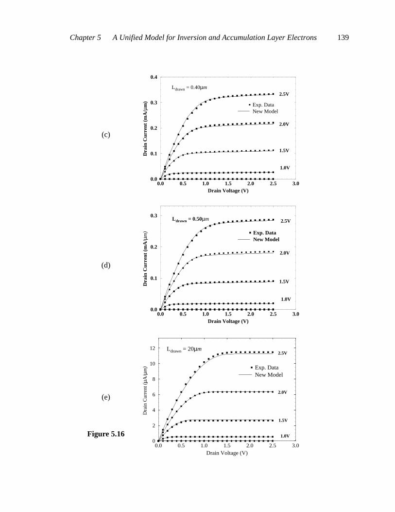
Chapter 5 A Unified Model for Inversion and Accumulation Layer Electrons 139
(c)
(d)
(e)
0.0 0.5 1.0 1.5 2.0 2.5 3.0Drain Voltage (V)
0.0
0.1
0.2
0.3
0.4
Dra
in C
urre
nt (
mA
/µm
)
Exp. DataNew Model
2.5V
2.0V
1.5V
1.0V
Ldrawn = 0.40µm
0.0 0.5 1.0 1.5 2.0 2.5 3.0Drain Voltage (V)
0.0
0.1
0.2
0.3
Dra
in C
urre
nt (
mA
/µm
) Exp. DataNew Model
2.5V
2.0V
1.5V
1.0V
Ldrawn = 0.50µm
0.0 0.5 1.0 1.5 2.0 2.5 3.0Drain Voltage (V)
0
2
4
6
8
10
12
Dra
in C
urre
nt (
µA/µ
m) Exp. Data
New Model
2.5V
2.0V
1.5V
1.0V
Ldrawn = 20µm
Figure 5.16

Chapter 5 A Unified Model for Inversion and Accumulation Layer Electrons 140
wide range of device geometries and terminal biases.
5.7 Summary
Using 2D process and device simulations, it was shown in this chapter that the
parasitic series resistance in deep submicron LDD MOSFETs has become comparable to
the intrinsic channel resistance. It was demonstrated that conventional mobility models
formulated for the inversion layer fail to accurately reproduce the I-V characteristics of
LDD MOSFETs. In an effort to model the extrinsic resistance of the device, a model for
accumulation layer mobility was developed that considered phonon, surface roughness,
and Coulombic scattering in the accumulation layer.
A systematic simulation methodology was presented which emphasized the
consideration of the following issues for an accurate simulation of LDD MOSFETs:
• validity of 2D process simulation results
• extraction of contact resistance
• specification of contact-to-poly spacing
• extraction of effective electrical gate oxide thickness
• extraction of patterned channel length for deep submicron structures
• a unified model for inversion and accumulation layers
Excellent fits with measured I-V characteristics of a realistic 0.25µm technology
over a wide range of channel lengths and terminal biases were demonstrated with the help
of the proposed simulation methodology.

141
Chapter 6
Conclusion
6.1 Summary
In summary, we have examined the theoretical issues related to the modeling of
mobility and suggested new measurements to enhance existing calibration techniques. The
study of mobility was motivated by the fact that it is one of the most important parameter
affecting the I-V characteristics of MOSFETs. In that regard, two particular issues —
Coulomb scattering and LDD resistance — were studied that have emerged in recent years
due to the continued scaling of MOSFETs to deep submicron dimensions. The objective of
this research was to develop physically-based mobility models, and the approach taken to
achieve this was to start with a first-principles calculation of mobility, and then proceed to
semi-empirical and empirical forms by means of calibration techniques. The major
findings and results of this research are summarized below.
6.1.1 2D Coulombic Scattering in MOS inversion layers
1. A first-principles calculation of two dimensional Coulombic scattering was
performed for inversion layer electrons. It was demonstrated that for both
screened and unscreened scattering, the new 2D model exhibited better
agreement than classical 3D models.
2. A new systematic technique was presented for extraction of unscreened
Coulombic scattering that involved classical and quantum simulations and
required the use of I-V and C-V data.

Chapter 6 Conclusion 142
3. It was demonstrated that accurate prediction of threshold voltage and off-state
leakage current in heavily doped MOSFETs requires the use of well-calibrated
models for Coulombic scattering in device simulators.
6.1.2 A Semi-Empirical Model for the Generalized Mobility Curve
1. Semi-empirical models for phonon, surface roughness, and Coulombic
scattering were obtained from a first-principles calculation of the respective
terms. The total model was obtained via a Matthiessen’s rule summation of the
three terms.
2. It was demonstrated that the new model reproduced all the properties of the
universal and the generalized mobility curve.
3. The model was formulated in local form to exploit numerical properties of
moment-based device simulators.
6.1.3 A Unified Model for LDD MOSFETs
1. It was demonstrated through coupled 2D process and device simulations that in
deep submicron LDD MOSFETs, extrinsic resistance has become comparable
to channel resistance. Hence, accurate simulations require mobility models
valid in both regions.
2. A physically-based semi-empirical local mobility model for inversion and
accumulation layer electrons was presented that accurately reproduced the I-V
characteristics of MOSFETs down to 0.25µm gate lengths.
3. A systematic technique was presented for the calibration and validation of
mobility models that requires the independent extraction of contact resistance
from Kelvin test structures and effective oxide thickness from quasi-static C-V
measurements.
4. Finally, it was demonstrated that drift-diffusion device simulators can
accurately model the saturation region characteristics of MOSFETs down to
0.25µm gate lengths provided well-calibrated and physically-based low-field
mobility models are used.

Chapter 6 Conclusion 143
6.2 Future Work
Based on the findings of this research, future work is suggested in the following areas:
1. The unified mobility model presented in Chapter 5 was implemented in the
drift-diffusion (DD) transport equation. It was recognized in the course of this
research that for gate lengths shorter than 0.25µm, the DD formulation failed
to give accurate results due to hot-carrier effects occurring in the channel. To
extend the model to shorter channel lengths, it is suggested that the low-field
mobility model be implemented in either an energy-transport or a
hydrodynamic formulation of carrier transport.
2. One consequence of MOSFET scaling — the emergence of Coulombic
scattering due to channel impurities — was considered in this research. The
other consequence is the emergence of quantum mechanical effects in the
channel due to thinner dielectrics. Significant error is introduced in charge
calculations if only classical equations are solved. The ad hoc approach used in
this thesis was to correct for this effect by extracting an effective oxide
thickness (see Section 5.6). Hence, a partial if not a full quantum treatment of
the inversion layer is required. The challenge would be to implement the
quantum mechanical effects in 2D device simulators such as PISCES without
adversely affecting the computation time.
3. In this thesis, existing mobility models were enhanced in two aspects:
inclusion of a physically-based model for Coulombic scattering, and
incorporation of a model for accumulation layer electrons. Since these two
effects have emerged in deep submicron MOSFETs, they need to be
incorporated in compact models for circuit simulation as well in order to
extend their range of applicability.
144
Bibliography
[1] S. A. Mujtaba, R. W. Dutton, and D. L. Scharfetter, “Semi-empirical local NMOSmobility model for 2-D device simulation incorporating screened minorityimpurity scattering,” in Proc. 5th Intl. Workshop on Numerical Modeling ofProcesses and Devices for Integrated Circuits (NUPAD), pp. 3-6, 1994.
[2] S. A. Mujtaba, S. Takagi, R.W. Dutton, “Accurate modeling of Coulombicscattering, and its impact on scaled MOSFETs,” in Symp. VLSI Technology Dig.Tech. Papers, pp. 99-100, 1995.
[3] S. A. Mujtaba, M. R. Pinto, D. M. Boulin, C. S. Rafferty, R. W. Dutton, “Anaccurate NMOS mobility model for 0.25µm MOSFETs,” in Proc. 6th Intl. Conf.Simulation of Semiconductor Devices and Processes (SISDEP), pp. 424-427,1995. Simulation of Semiconductor Devices and Processes, vol. 6, Edited H.Ryssel and P. Pichler, Springer-Verlag, Wein, Germany, 1995.
[4] S. A. Mujtaba and R. W. Dutton, “Design methodology for low power CMOStechnologies,” in Proc. Hierarchical Technology CAD — Process, Device, andCircuits, August 1995, Stanford University, Stanford, CA.
[5] C. Hu, “Future CMOS scaling and reliability,” Proc. IEEE, vol. 81, pp. 682-689,1993.
[6] Y. Taur, Y.-J. Mii, D. J. Frank, H.-S. Wong, D. A. Buchanan, S. J. Wind, S. A.Rishton, G. A. Sai-Halasz, and E. J. Nowak, “CMOS scaling into the 21st century:0.1µm and beyond,” IBM J. Res. & Dev., vol. 39, no. 1-2, pp. 245-60, 1995.

Bibliography 145
[7] S. M. Sze, Physics of Semiconductor Devices, 2nd Edition, New York: Wiley1981.
[8] T. Ando, A. B. Fowler, and F. Stern, “Electronic properties of two-dimensionalsystems,” Rev. Mod. Phys., vol. 54, no. 2, pp. 437-672, 1982.
[9] S. Takagi, M. Iwase, and A. Toriumi, “On the universality of inversion-layermobility in n- and p-channel MOSFETs,” in IEDM Tech. Dig., pp. 398-401, 1988.
[10] S. Takagi, A. Toriumi, M. Iwase, and H. Tango, “On the universality ofinversion-layer mobility in Si MOSFETs: Part I — effects of substrate impurityconcentration,” IEEE Trans. Elec. Dev., vol. 41, no. 12, pp. 2357-62, 1994.
[11] S. Takagi, A. Toriumi, M. Iwase, and H. Tango, “On the universality ofinversion-layer mobility in Si MOSFETs: Part II — effects of surface orientation,”IEEE Trans. Elec. Dev., vol. 41, no. 12, pp.2363-8, 1994.
[12] E. Conwell and V. Weisskopf, “Theory of impurity scattering in semiconductors,”Phys. Rev., vol. 77, no. 3, pp. 388-390, 1950.
[13] H. Brooks, “Scattering by ionized impurities in semiconductors,” Phy. Rev., vol.83, p. 879, 1951.
[14] N. W. Ashcroft and N. D. Mermin, Solid State Physics, Saunders College,Philadelphia, 1976.
[15] M. Lundstrom, Fundamentals of Carrier Transport, Addison-Wesley, Reading,MA, 1990.
[16] L. Boltzmann, Lectures on gas theory, University of California Press, Berkeley,1964, translated by S. G. Brush.
[17] J. J. Duderstadt and W. R. Martin, Transport Theory, Wiley, New York, 1979.
[18] P. W. Bridgman, “Note on the principle of detailed balancing,” Phys. Rev., vol. 31,pp. 101-102, 1928.
[19] J. E. Chung, M. C. Jeng, J. E. Moon, P. K. Ko, C. Hu, “Performance and reliabilitydesign issues for deep-submicrometer MOSFETs,” IEEE Trans. Elec. Dev., vol.38, no. 3, pp. 545-553, 1991.
[20] G. Baccarani and G. A. Sai-Halasz, “Spreading resistance in submicronMOSFETs”, IEEE Elec. Dev. Letters, vol. 4, no. 2, pp. 227-29, 1983.

Bibliography 146
[21] M. H. Seavey, “Source and drain resistance determination for MOSFETs,” IEEEElec. Dev. Letters, vol. 5, no. 11, pp. 479-481, 1984.
[22] K. K. Ng, R. J. Bayruns, and S. C. Fang, “The spreading resistance of MOSFETs”,IEEE Elec. Dev. Letters, vol. 6, no. 4, pp. 195-198, 1985.
[23] K. K. Ng and W. T. Lynch, “Analysis of the gate-voltage-dependent seriesresistance of MOSFETs,” IEEE Tran. Elec. Dev., vol. 33, no. 7, pp. 965-972, 1986.
[24] F. M. Klaasseen, P. T. F. Biermans, and R. M. D. Velghe, “The series resistance ofsubmicron MOSFETs and its effect on their characteristics,” J. De Physique,Colloque C4, suppl. 9, pp. 257-260, Sep. 1988.
[25] J. Lee, M. B. Lee, S. Y. Lee, K. N. Kang, K. S. Yoon, “Simple model forgate-voltage dependent parasitic resistance in short channel lightly doped drainmetal oxide semiconductor field effect transistor,” Jap. J. Appl. Phys., vol. 30, no.4A, pp. L 535-L 537, 1991.
[26] B. Lemaitre, “An improved analytical LDD-MOSFET model for digital andanalog circuit simulation for all channel lengths down to deep-submicron,” inIEDM Tech. Dig., pp. 333-336, 1991.
[27] M. R. Pinto, D. M. Boulin, C. S. Rafferty, R. K. Smith, W. M. Coughran Jr., I. C.Kizilyalli, M. J. Thoma, “Three-dimensional characterization of bipolar transistorsin a submicron BiCMOS technology using integrated process and devicesimulation,” in IEDM Tech. Dig., pp. 923-926, 1992.
[28] M. R. Pinto, “Simulation of ULSI device effects,” Electrochem. Soc. Proc., vol.91-11, pp. 43-51, 1991.
[29] S. A. Schwarz and S. E. Russek, “Semi-Empirical equations for electron velocityin Silicon: Part II — MOS Inversion layer,” IEEE Trans. Elec. Dev., vol. 30, no.12, pp. 1634-1639, 1983.
[30] C. Lombardi, S, Manzini, A. Saporito, and M. Vanzi, “A Physically based mobilitymodel for numerical simulation of nonplanar devices,” IEEE Trans. CAD, vol. 7,no. 11, pp. 1164-71, 1988.
[31] T. Nishida and C. T. Sah, “A physically based mobility model for MOSFETnumerical simulation,” IEEE Trans. Elec. Dev., vol. 34, no. 2, pp. 310-320, 1987.
[32] H. Shin, A. F. Tasch, C. M. Maziar, and S. K. Banerjee, “A new approach to verifyand derive a transverse-field-dependent mobility model for electrons in MOS

Bibliography 147
inversion layers,” IEEE Trans. Elec. Dev., vol. 36, no. 6, pp. 1117-1123, 1989.
[33] S. C. Sun and J. D. Plummer, “Electron mobility in inversion and accumulationlayers on thermally oxidized silicon surfaces,” IEEE Trans. Elec. Dev., vol. 27, no.8, pp. 1497-1508, 1980.
[34] D. M. B. Klaassen, “A Unified mobility model for device simulation — I. Modelequations and concentration dependence,” Sol. State Elec., vol. 35, no. 7, pp.953-959, 1992.
[35] W. Hansch and M. Miura-Mattausch, “The hot electron problem in smallsemiconductor devices,” J. Appl. Phys., vol. 60, no. 2, pp. 650-656, 1986.
[36] K. Krisch, AT&T Bell Laboratories, Private Communication.
[37] D. M. Boulin, W. M. Mansfield, K. J. O’Connor, J. Bevk, D. Brasen, M. Cheng, R.A. Cerilli, S. A. Eshraghi, M. L. Green, K. V. Guinn, S. J. Hillenius, D. E.Ibboston, D. C. Jacobson, Y. O. Kim, C. A. King, R. C. Kistler, F. P. Klemens, K.S. Krisch, A. Kornblit, J. T. C. Lee, L. Manchanda, S. C. McNevin, S. V. Moccio,D. P. Monroe, K. K. Ng, M. L. O’Malley, C. S. Rafferty, G. P. Schwartz, S. Vaidya,G. R. Weber, L. C. Feldman, M. R. Pinto, T. Itani, T. Tounai, K. Kasama, H.Miyamoto, E. Ikawa, E. Hasagawa, A. Ishitani, H. Ito, T. Horiuchi, S. Saito, M.Nakamae, “A Symmetric 0.25µm CMOS Technology for Low-Power,High-Performance ASIC Applications Using 248nm DUV Lithography,” in Symp.VLSI Technology Dig. Tech. Papers, pp. 65-66, 1995.
[38] C. S. Rafferty, H.-H. Vuong, S. A. Eshraghi, M. D. Giles, M. R. Pinto, S. J.Hillenius, “Explanation of reverse short channel effect by defect gradient,” inIEDM Tech. Dig., pp. 311-314, 1993.
[39] G. Hu, C. Chang, and Y.-T. Chia, “Gate-voltage dependent effective channellength and series resistance of LDD MOSFET’s,” IEEE Trans. Elec. Dev., vol.ED-34, no. 12, pp. 2469-75, 1987.
[40] F. J. Blatt, “Scattering of carriers by ionized impurities in semiconductors,” J.Phys. Chem. Solids, vol. 1, pp. 262-269, 1957.
[41] D. K. Ferry, Semiconductors, Macmillan, New York, 1991.
[42] B. R. Nag, Theory of Electrical Transport in Semiconductors, Pergamon Press,New York, 1972.
[43] A. G. Sabnis and J. T. Clemens, “Characterization of the electron mobility in the

Bibliography 148
inverted <100> Si Surface,” in IEDM Tech. Dig., pp. 18-21, 1979.
[44] M. S. Lin, “A better understanding of the channel mobility of Si MOSFETs basedon the physics of quantized subbands,” IEEE Trans. Elec. Dev., vol. 35, no. 12, pp.2406-2411, 1988.
[45] F. Stern, “Self-consistent results for n-Type Si Inversion Layers,” Phys. Rev. B,vol. 5, no. 12, pp. 4891-4899, 1972.
[46] D. K. Ferry, K. Hess, and P. Vogl, “Physics and Modeling of SubmicronInsulated-Gate Field-Effect Transistors. II -- transport in the quantized inversionlayer,” in VLSI Electronics, Microstructure Science, vol. 2, Academic Press, NewYork, pp. 67-103, 1981.
[47] C. T. Sah, T. H. Ning, and L. L. Tschopp, “The scattering of electrons by surfaceoxide charges and by lattice vibrations at the silicon-silicon dioxide interface,”Surf. Sci., vol. 32, pp. 561-575, 1972.
[48] F. Stern, “Quantum properties of surface space-charge layers,” in CRC CriticalReviews in Solid State Sciences, vol. 4, pp. 499-514, 1974.
[49] A. P. Gnadinger and H. E. Tally, “Quantum mechanical calculation of the carrierdistribution and the thickness of the inversion layer of a MOS field-effecttransistor,” Sol. State Elec., vol. 13, pp. 1301-1309, 1970.
[50] F. Stern and W. E. Howard, “Properties of Semiconductor Surface InversionLayers in the Electric Quantum Limit,” Phys. Rev., vol. 163, no. 3, pp. 816-835,1967.
[51] F. F. Fang and W. E. Howard, “Negative field-effect mobility on (100) Sisurfaces,” Phys. Rev. Lett., vol. 16, pp. 797-799, 1966.
[52] A. Harstein, T. H. Ning, and A. B. Fowler, “Electron scattering in SiliconInversion Layers by oxide charge and surface roughness,” Surf. Sci., vol. 58, pp.178-181, 1976.
[53] K. Lee, J. S. Choi, S. P. Sim, and C. K. Kim, “Physical understanding ofLow-Field Carrier Mobility in Silicon MOSFET Inversion Layer,” IEEE Trans.Elec. Dev., vol. 38, no. 8, pp. 1905-1912, 1991.
[54] M. R. Pinto, C. S. Rafferty, H. R. Yeager and R. W. Dutton, “PISCES-IIBSupplementary Report,” Stanford University, Stanford, California, 1985.

Bibliography 149
[55] M. R. Pinto, Comprehensive Semiconductor Device Simulation for Silicon ULSI,Ph.D. thesis, Stanford University, 1990.
[56] R. W. Dutton and Z. Yu, Technology CAD: computer simulation of IC processesand devices, Kluwer Academic, Boston, 1993.
[57] B. Herndon, A Methodology for the Parallelization of PDEs: Application toSemiconductor Device Physics, Ph.D. thesis, Stanford University, 1995.
[58] S. Kawaji, “The Two-Dimensional Lattice Scattering Mobility in a SemiconductorInversion Layer,” J. Phys. Soc. Japan, vol. 27, no. 4, pp. 906-908, 1969.
[59] C. M. Wolfe, N. Holonyak, and G. E. Stillman, Physical Properties ofSemiconductors, Prentice-Hall, New Jersey, 1989.
[60] K. Hess, Advanced Theory of Semiconductor Devices, Prentice-Hall, New Jersey,1988.
[61] F. J. Morin and J. P. Maita, “Electrical properties of silicon containing arsenic andboron,” Phys. Rev., vol. 96, pp. 28-35, 1954.
[62] S. S. Li and W. R. Thurber, “The dopant density and temperature dependence ofelectron mobility and resistivity in n-type silicon,” Solid State Elec., vol. 20, p.609-616, 1977.
[63] B. K. Ridley, “The electron-phonon interaction in quasi-two-dimensionalsemiconductor quantum-well structures,” J. Phys. C: Solid State Phys., vol. 15, pp.5899-5917, 1982.
[64] B. K. Ridley, “Electron-Phonon interaction in 2D systems,” in Hot Carriers inSemiconductor Nanostructures: Physics and Applications, Edited by J. Shah, pp.17-51, 1992.
[65] T. Ando, “Screening effect and quantum transport in a silicon inversion layer instrong magnetic fields,” J. Phys. Soc. Japan, vol. 43, pp. 1616-1626, 1977.
[66] Y. C. Cheng, “Electron Mobility in an MOS Inversion Layer,” in Proc. 3rd Conf.Solid State Devices, pp. 173-180, 1971.
[67] K. Masaki, K. Taniguchi, C. Hamaguchi, and M. Iwase, “Temperature Dependenceof Electron Mobility in Si Inversion Layers,” Japanese J. Appl. Phys., vol. 30, no.11A, pp. 2734-2739, 1991.

Bibliography 150
[68] Y. Matsumoto and Y. Uemura, “Scattering Mechanism and Low TemperatureMobility of MOS Inversion Layers,” Japan J. Appl. Phys., vol. 13, Supp. 2, Part 2,pp. 367-370, 1974.
[69] Y. C. Cheng and E. A. Sullivan, “On the role of scattering by surface roughness insilicon inversion layers,” Surface Science, vol. 34, pp. 717-731, 1973.
[70] L. I. Schiff, Quantum Mechanics, McGraw-Hill, New York, 1955.
[71] J. R. Meyer and F. J. Bartoli, “Phase-shift calculation of ionized impurityscattering in semiconductors,” Phys. Rev. B, vol. 23, no. 10, pp. 5413-5427, 1981.
[72] D. K. Ferry, “Effects of Surface Roughness in Inversion layer transport,” in IEDMTech. Dig., pp. 605-608, 1984.
[73] A. C. Smith, J. F. Janak, and R. B. Adler, Electronic conduction in solids,McGraw-Hill, New York, 1967.
[74] Donald P. Monroe, AT&T Bell Laboratories, Private Communication.
[75] C. G. Sodini, T. W. Ekstedt, and J. L. Moll, “Charge accumulation and mobility inthin dielectric MOS transisitors,” Sol.-State Elec., vol. 25, pp. 833-841, 1982.
[76] S. Takagi, M. Iwase, and A. Toriumi, in Extended Abstracts of the 22nd. Conf. Sol.State Dev. Mat., pp. 275-278, 1990.
[77] J. T. Watt and J. D. Plummer, “Universal mobility-field curves electrons and holesin MOS inversion layers,” in Symp. VLSI Technology Dig. Tech. Papers, pp. 81-82,1987.
[78] C. L. Huang and G. Sh. Gildenblat, “Measurement and Modeling of the n-ChannelMOSFET Inversion Layer Mobility and Device Characteristics in the TemperatureRange 60-300K,” IEEE Trans. Elec. Dev., vol. ED-37, pp. 1289-1300, 1990.
[79] N. D. Arora and G. Sh. Gildenblat, “A semi-empirical model of the MOSFETinversion layer mobility for low-temperature operation,” IEEE Trans. Elec. Dev.,vol. ED-34, no. 1, pp. 89-93, 1987.
[80] H. Shin, G. M. Yeric, A. F. Tasch, and C. M. Maziar, “Physically-based models foreffective mobility and local-field mobility of electrons in MOS Inversion layers,”Solid-State Elec., vol. 34, no. 6, pp. 545-552, 1991.
[81] K. Masaki, C. Hamaguchi, K. Taniguchi, and M. Iwase, “Electron mobility in Si

Bibliography 151
inversion layers,” Jap. J. of Appl. Phys., vol. 28, no. 10, pp. 1856-1863, 1989.
[82] M. Shirahata, H. Kusano, N. Kotani, S. Kusanoki, and Y. Akasaka, “A mobilitymodel including the screening effect in MOS inversion layer,” IEEE Tran. CAD,vol. 11, no. 9, pp. 1114-1118, 1992.
[83] C. Kittel and H. Kroemer, Thermal Physics, 2nd Edition, Freeman, New York,1980.
[84] K. Shimohigashi and K. Seki, “Low-voltage ULSI design,” J. Solid-State Circuits,vol. 28, no. 4, pp. 408-413, 1993.
[85] H. Haug and S. W. Koch, Quantum Theory of the Optical and Electronicproperties of semiconductors, 2nd Edition, World Scientific, Singapore, 1990.
[86] N. Iwamoto, “Static local-field corrections of two-dimensional electron liquids,”Phys. Rev. B, vol. 43, no. 3, pp. 2174-2182, 1991.
[87] C. Kittel, Introduction to Solid State Physics, 6th Edition, Wiley, New York, 1986.
[88] G. Y. Hu and R. F. O’Connell, “Polarisability of a two-dimensional electron gasincluding fluctuation effects,” J. Phys. C: Solid State Phys., vol. 21, pp.4325-4331, 1988.
[89] F. F. Fang, A. B. Fowler, and A. Harstein, “Effective mass and collision time of(100) Si surface electrons,” Phys. Rev., B 16, pp. 4446-4454, 1977.
[90] F. F. Fang, “2DEG in strained Si/SiGe heterostructures,” Surf. Sci., vol. 305, pp.301-306, 1994.
[91] C. -L. Huang, J. V. Faricelli, and N. D. Arora, “A new technique for measuringMOSFET inversion layer mobility,” IEEE Trans. Elec. Dev., vol. 40, no. 6, pp.1134-1139, 1993.
[92] C. -L. Huang and N. D. Arora, “Characterization and modeling of the n- andp-channel MOSFETs inversion-layer mobility in the range 25-125°C,” Solid-StateElectronics, vol. 37, no. 1, pp. 97-103, 1994.
[93] R. S. Muller and T. I. Kamins, Device Electronics for Integrated Circuits, 2nd.Edition, Wiley, New York, 1986.
[94] J. Koomen, “Investigation of the MOST channel conductance in weak inversion”Solid-State Electronics, vol. 16, pp. 801-809, 1973.

Bibliography 152
[95] P. M. D. Chow and K. L. Wang, “A new ac technique for accurate determination ofchannel charge and mobility in very thin gate MOSFETs,” IEEE Trans. Elec. Dev.,vol. 33, pp. 1299-1304, 1986.
[96] S. Takagi, Toshiba Corp., Private Communication.
[97] S. Malhi and P. Chatterjee, “1-V microsystems-scaling on schedule for personalcommunications,” IEEE Circuits and Devices, pp. 13-17, 1994.
[98] T. H. Ning and C. T. Sah, “Theory of scattering of electrons in anondegenerate-semiconductor-surface inversion layer by surface oxide charges,”Phys. Rev. B, vol. 6, no. 12, pp. 4605-4613, 1972.
[99] F. Gamiz, J. A. Lopez-Villanueva, J. A. Jimenez-Tejada, I. Melchor, A. Palma, “Acomprehensive model for Coulomb scattering in inversion layers,” J. Appl. Phys.,vol. 75, no. 2, pp. 924-934, 1994.
[100] A. Gold, “Electronic transport properties of a two-dimensional electron gas in asilicon quantum-well structure at low temperature,” Phys. Rev. B, vol. 35, no. 2,pp. 723-733, 1987.
[101] J. Lee, H. N. Spector, and V. K. Arora, “Impurity scattering limited mobility in aquantum well heterojunction,” J. Appl. Phys., vol. 54, no. 2, pp. 6995-7004, 1983.
[102] D. Monroe, Y. H. Xie, E. A. Fitzgerald, P. J. Silverman, G. P. Watson,“Comparison of mobility-limiting mechanisms in high-mobiliy Si1-xGexheterostructures,” J. Vac. Sci. Technol. B, vol. 11, no. 4, pp. 1731-1737, 1993.
[103] K. Hess, “Impurity and phonon scattering in layered structures,” Appl. Phys. Lett.,vol. 35, no. 7, pp. 484-486, 1979.
[104] A. Gold, “Scattering time and single-particle relaxation time in a disorderedtwo-dimensional electron gas,” Phys. Rev. B, vol. 38, no. 15, pp. 10798-10811,1988.
[105] D. Pines, Elementary excitations in solids, Benjamin, New York, 1963.
[106] M. V. Fischetti and S. E. Laux, “Monte Carlo study of electron transport in siliconinversion layers,” Phys. Rev. B, vol. 48, no. 4, pp. 2244-2274, 1993.
[107] J. A. Lopez-Villanueva, I. Melchor, F. Gamiz, J. Banqueri, J. A. Jimenez-Tejada,“A model for the quantized accumulation layer in metal-insulator-semiconductorstructures,” Solid-State Electronics, vol. 38, no. 1, pp. 203-210, 1995.

Bibliography 153
[108] Conor Rafferty, AT&T Bell Laboratories, Private Communication.
[109] E. H. Nicollian and J. R. Brews, MOS (Metal Oxide Semiconductor) Physics andTechnology, Wiley, New York, 1982.
[110] M. J. van Dort, P. H. Woerlee, A. J. Walker, C. A. H. Juffermans, and H. Lifka,“Influence of high substrate doping levels on the threshold voltage and themobility of deep-submicrometer MOSFET’s,” IEEE Trans. Elec. Dev., vol. 39, no.4, pp. 932-937, 1992.
[111] D. Boulin, AT&T Bell Laboratories, Private Communication.
[112] S. Biesemans and K. D. Meyer, “Analytical calculation of the subthreshold slopeincrease in short channel MOSFET’s by taking the drift component into account,”in Proc. Solid State Dev. Mat., pp. 892-894, 1994.
[113] K. K. Ng and J. R. Brews, “Measuring the effective channel length of MOSFETs,”IEEE Circuits and Devices Mag., vol. 6, no. 6, pp. 33-38, Nov. 1990.
[114] H.-H Vuong, C. S. Rafferty, M. J. McLennan, and J. Lentz, “Industrial perspectivebased on PROPHET,” in CAD for IC’s — Process, Device, and Circuits, StanfordUniversity, Stanford, Calif., August 1994.
[115] S. J. Proctor, L. W. Linholm, and J. A. Mazer, “Direct measurement of interfacialcontact resistance, end contact resistance, and interfacial contact layer uniformity,”IEEE Trans. Elec. Dev., vol. 30, pp. 1535-1542, 1983.
[116] C. Y. Lu, J. M. Sung, H. C. Kirsch, S. J. Hillenius, T. E. Smith, and L. Manchanda,
“Anamolous C-V characteristics of implanted poly MOS structure in n+/p+
dual-gate CMOS technology,” IEEE Elec. Dev. Lett., vol. 10, no. 5, pp. 192-194,1989.
[117] M. R. Pinto, J. Bude, and C. S. Rafferty, “Simulation of ULSI silicon MOSFETs,”in Proc. VPAD, pp. 22-25, 1993.
[118] Y. Ohkura, “Quantum effects in Si n-MOS inversion layer at high substrateconcentration,” Solid-State Elec., vol. 33, no. 12, pp. 1581-1585, 1990.
[119] C. -Y. Hu, D. L. Kencke, S. Banerjee, B. Bandyopadhyay, E. Ibok, and S. Garg,“Determining effective dielectric thicknesses of metal-oxide-semiconductorstructures in accumulation mode,” Appl. Phys. Lett., vol. 66, no. 13, pp. 1638-40,1995.