Advanced Low Power High Speed Nonlinear Signal Processing ... · of signal processing with energy e...
16
Journal of Signal Processing Systems manuscript No. (will be inserted by the editor) Advanced Low Power High Speed Nonlinear Signal Processing: An Analog VLSI Example. Giuseppe Oliveri · Mohamad Mostafa · Werner G. Teich · J¨ urgen Lindner · Hermann Schumacher Received: date / Accepted: date Abstract Despite the progress made in digital signal processing during the last decades, the constraints im- posed by high data rate communications are becoming ever more stringent. Moreover mobile communications raised the importance of power consumption for sophis- ticated algorithms, such as channel equalization or de- coding. The strong link existing between computational speed and power consumption suggests an investigation of signal processing with energy efficiency as a promi- nent design choice. In this work we revisit the topic of signal processing with analog circuits and its potential to increase the energy efficiency. Channel equalization is chosen as an application of nonlinear signal process- ing, and a vector equalizer based on a recurrent neural network structure is taken as an example to demon- strate what can be achieved with state of the art in VLSI design. We provide an analysis of the equalizer, including the analog circuit design, system-level simula- tions, and comparisons with the theoretical algorithm. Giuseppe Oliveri 1 Tel.: +49 (0)731 5031595 E-mail: [email protected] Mohamad Mostafa 2 E-mail: [email protected] Werner G. Teich 3 E-mail: [email protected] J¨ urgen Lindner 3 E-mail: [email protected] Hermann Schumacher 1 E-mail: [email protected] 1 Institute of Electron Devices and Circuits, Ulm University, Ulm, Germany 2 Institute of Communications and Navigation, German Aerospace Center, Wessling, Germany 3 Institute of Communications Engineering, Ulm University, Ulm, Germany First measurements of our analog VLSI circuit confirm the possibility to achieve an energy requirement of a few pJ/bit, which is an improvement factor of three to four orders of magnitude compared with today’s most energy efficient digital circuits. Keywords Nonlinear signal processing · Energy requirements · Analog VLSI · Vector equalization · Recurrent neural networks 1 Introduction Energy efficiency became an essential aspect in recent years, especially for mobile devices. The most recent Green500 [2] and Top500 [21] rankings show that the most efficient heterogeneous supercomputers can reach peak performance of about five GFLOPS/Watt. De- spite the effort to increase this value, the current trend shows an ever-growing difficulty in improving the en- ergy efficiency of digital circuits [3]. As an example, in [14] the authors identify both physical and architec- tural limitations of modern processors, and predict that those barriers may severely hamper the reduction of the required energy per operation in the future. We address here alternatives offered by analog cir- cuits. Some authors of earlier work in the field of ad- vanced analog processing concluded that analog sys- tems have the potential to improve the efficiency sub- stantially [12]. Moreover, depending on the application, there might be no need for additional A/D conversion [4]. Analog signal processing is already advantageously used for low-power low-frequency applications [22] and is gaining momentum for applications in the millimeter- wave frequency range [20]. Related to our work are activities in building cir- cuits emulating functions of natural neural networks,
Transcript of Advanced Low Power High Speed Nonlinear Signal Processing ... · of signal processing with energy e...
Journal of Signal Processing Systems manuscript No.(will be inserted by the editor)
Advanced Low Power High Speed Nonlinear Signal Processing:An Analog VLSI Example.
Giuseppe Oliveri · Mohamad Mostafa · Werner G. Teich · Jurgen
Lindner · Hermann Schumacher
Received: date / Accepted: date
Abstract Despite the progress made in digital signal
processing during the last decades, the constraints im-
posed by high data rate communications are becoming
ever more stringent. Moreover mobile communications
raised the importance of power consumption for sophis-
ticated algorithms, such as channel equalization or de-
coding. The strong link existing between computational
speed and power consumption suggests an investigation
of signal processing with energy efficiency as a promi-
nent design choice. In this work we revisit the topic of
signal processing with analog circuits and its potential
to increase the energy efficiency. Channel equalization
is chosen as an application of nonlinear signal process-
ing, and a vector equalizer based on a recurrent neural
network structure is taken as an example to demon-
strate what can be achieved with state of the art inVLSI design. We provide an analysis of the equalizer,
including the analog circuit design, system-level simula-
tions, and comparisons with the theoretical algorithm.
Giuseppe Oliveri1
Tel.: +49 (0)731 5031595E-mail: [email protected]
Mohamad Mostafa2
E-mail: [email protected]
Werner G. Teich3
E-mail: [email protected]
Jurgen Lindner3
E-mail: [email protected]
Hermann Schumacher1
E-mail: [email protected]
1 Institute of Electron Devices and Circuits,Ulm University, Ulm, Germany2 Institute of Communications and Navigation,German Aerospace Center, Wessling, Germany3 Institute of Communications Engineering,Ulm University, Ulm, Germany
First measurements of our analog VLSI circuit confirm
the possibility to achieve an energy requirement of a
few pJ/bit, which is an improvement factor of three to
four orders of magnitude compared with today’s most
energy efficient digital circuits.
Keywords Nonlinear signal processing · Energy
requirements · Analog VLSI · Vector equalization ·Recurrent neural networks
1 Introduction
Energy efficiency became an essential aspect in recent
years, especially for mobile devices. The most recent
Green500 [2] and Top500 [21] rankings show that the
most efficient heterogeneous supercomputers can reachpeak performance of about five GFLOPS/Watt. De-
spite the effort to increase this value, the current trend
shows an ever-growing difficulty in improving the en-
ergy efficiency of digital circuits [3]. As an example,
in [14] the authors identify both physical and architec-
tural limitations of modern processors, and predict that
those barriers may severely hamper the reduction of the
required energy per operation in the future.
We address here alternatives offered by analog cir-
cuits. Some authors of earlier work in the field of ad-
vanced analog processing concluded that analog sys-
tems have the potential to improve the efficiency sub-
stantially [12]. Moreover, depending on the application,
there might be no need for additional A/D conversion
[4]. Analog signal processing is already advantageously
used for low-power low-frequency applications [22] and
is gaining momentum for applications in the millimeter-
wave frequency range [20].
Related to our work are activities in building cir-
cuits emulating functions of natural neural networks,

2 Giuseppe Oliveri et al.
e.g. the European “Human Brain” project [13]. In this
context it is common to use the term “neuromorphic
computing”, see also the early work by Mead [15]. In
contrast to neuromorphic computing, our focus is more
on common signal processing algorithms, usually real-
ized today with digital circuits or digital processors.
To demonstrate how far the energy efficiency can
be increased with state of the art VLSI design, in this
work, a vector equalizer (VE) [11] serves as an exam-
ple of a functional block requiring nonlinear processing.
The nonlinearity offers the chance to use analog circuits
out of their conventional field of linear signal processing,
with all its disadvantages, like accumulation of noise
and inaccuracies of circuits elements. The correspond-
ing algorithms achieve results as robust as their digital
counterparts. This is no surprise, since “digital circuits”
are in essence analog circuits with strong nonlinearities.
The paper is organized as follows: in Section 2 we
explain the background of our application, while in Sec-
tion 3 we analyze the structure of the algorithm. In Sec-
tion 4 we detail the design steps and the components
needed to implement a real-valued vector equalizer in
SiGe BiCMOS technology. Section 5 expands the theory
of the transmission model, of the algorithm, and of the
design steps, in order to handle a complex-valued vector
equalization. Sections 6 and 7 discuss simulation results
of the vector equalizer. Included is the analysis of the
penalty in the BER, introduced by a finite resolution
of the equalizer’s weights. Section 8 highlights the im-
provement in the energy requirement that is achievable
with an analog circuit design, while Section 9 shows
measurements on a real chip. Conclusions in Section 10
close the paper.
2 Background
The background for our application is an uncoded dig-
ital transmission over radio channels with multiple an-
tennas (multiple-input-multiple-output, MIMO). We as-
sume a linear modulation scheme. Fig. 1 shows a model
for such a transmission, which is a discrete-time model
on a symbol basis. More about this model and its re-
lation to the continuous-time (physical) transmission
model can be found in [11]. For a real-valued trans-
mission model the quantities in Fig. 1 are defined as
follows:
– k is the discrete-time symbol interval variable;
– x(k) is the transmit symbol vector of length N at
symbol interval k. We assume binary phase shift
keying (BPSK) modulation, i.e. xi(k) ∈ −1,+1and the transmit symbol alphabet Ax contains 2N
possible transmit vectors of length N ;
Fig. 1 Discrete-time transmission model on a symbol ba-sis for an uncoded transmission with linear modulation overMIMO channels.
– R(k) is the discrete-time channel matrix on a sym-
bol basis. Its size is (N × N), it is hermitian and
positive semidefinite. We assume that the channel
state is known, with this information used to ap-
propriately configure the vector equalizer;
– ne(k) is a sample function of an additive Gaussian
noise vector process with zero mean and covariance
matrix given by Φnene(k) = N0
2 · R(k). N0 is the
single-sided noise power spectral density;
– x(k) = R(k) ∗ x(k) + ne(k) is the received symbol
vector. ∗ denotes matrix-vector convolution [11];
– x(k) ∈ Ax is the decided vector at the output of the
vector equalizer (VE).
R(k) includes the antennas at the transmit and re-
ceive sides, the transmit impulses, and the multipath
propagation on the radio channel as well. In general it
is a sequence of matrices with respect to the symbol
interval variable k. Because we assume here no inter-
ference between symbol vectors (or “blocks”), k can be
omitted and it is sufficient to consider a transmission
of isolated vectors. The model in Fig. 1 can then be de-
scribed mathematically as in Eq. (1). The non-diagonal
elements R\d of the channel matrix lead to interference
between the components of the transmitted vectors at
the receive side. Refer to [11] for more details.
x = R · x+ ne,
x = Rd · x︸ ︷︷ ︸signal
+ R\d · x︸ ︷︷ ︸interference
+ ne︸︷︷︸additive noise
,
R = Rd︸︷︷︸diagonal elements
+ R\d︸︷︷︸non-diagonal elements
.
(1)
The computational complexity of the optimum vec-
tor equalization (i.e. maximum likelihood, ML) grows
exponentially with N . Because this will result in an un-
realistic number of operations per symbol vector, sub-
optimum schemes have to be used. Our approach is to
use a recurrent neural network (RNN). The VE-RNN

Advanced Low Power High Speed Nonlinear Signal Processing: An Analog VLSI Example. 3
does not need a general training algorithm like back-
propagation, the entries of R can be measured and di-
rectly related to the weights of the RNN.
The application of the RNN as a vector equalizer has
been discussed first in the context of multiuser detection
for code division multiple access (CDMA) transmission
systems [8,24,16], see also [23,5]. It can be shown that
this RNN tries to maximize the likelihood function of
the optimum VE. In general it converges to a local max-
imum, but in many cases this local maximum turns out
to be close to or identical with the global maximum,
see e.g. [6].
3 Continuous-Time Recurrent Neural Network
The VE-RNN discussed before relies on a discrete-time
RNN. Analog circuit design requires continuous-time
RNNs [17], which have also been known for long time.
The dynamic behavior is described by a set of first order
nonlinear differential equations as in Eq. (2), where:
– t is the continuous-time evolution time variable;
– e is the external input vector of length N , where
N is the length of the transmit symbols, and corre-
sponds to the number of neurons in the RNN;
– T is a diagonal matrix with time constants τi on its
main diagonal;
– W is a (N ×N) weights matrix with entries wii′ ;
– W0 is a diagonal matrix with entries wi0 on its main
diagonal;
– u(t) is the state vector of length N ;
– v(t) is the corresponding output vector;
– v(t) = HD [v(t)] is the corresponding hard decision
(HD) output vector;
– ψi(·) is the ith element-wise activation function.
T · du(t)
dt= −u(t) +W · v(t) +W 0 · e,
v(t) = ψ [u(t)]
= [ψ1[u1(t)], ψ2[u2(t)], ..., ψN [uN (t)]]T,
v(t) = HD [v(t)]
= [HD1[v1(t)],HD2[v2(t)], ...,HDN [vN (t)]]T.
(2)
Fig. 2 shows a resistance-capacitance structure for
a real-valued continuous-time RNN [7]. The stability of
this RNN in the sense of Lyapunov has been intensively
investigated, e.g. in [10]. τi = Ri ·Ci is the time constant
of the i-th neuron. The weights in Eq. (2) above are
related to the resistors in Fig. 2 by normalization as
follows: wii′ = Ri
Rii′, wi0 = Ri
Ri0. To distinguish between
Fig. 2 Resistance-capacitance structure of a real-valued re-current neural network in continuous-time domain.
resistors and channel matrix, the symbol for the channel
matrix is bold.
3.1 Equalization based on Continuous-Time Recurrent
Neural Networks
The vector equalizer discussed in Section 2 works on a
symbol basis and is discrete in time. This means that
the clock for the VE is kTs, with k being the discrete
time variable and Ts the symbol interval for the digital
transmission. The RNN in Fig. 2 works equally with
the parallel input of a symbol vector, but is continu-
ous in time. In order to connect the vector equalizer of
Fig. 1 with the network of Fig. 2, the following condi-
tions must be fulfilled, cf. Eqs. (1), (2):
– The continuous-time RNN requires a minimum in-
terval of time to perform the equalization of a vec-
tor. This time slot is here defined as the total equal-
ization time tequ. It follows that the symbol interval
Ts for the digital transmission is constrained by the
equalization time, i.e. Ts ≥ tequ;
– e = x: the external input vector of the RNN repre-
sents the received symbol vector;
– v(tequ) = x: the output vector of the RNN – after
an equalization is performed and after the hard de-
cision – is coincident with the decided vector of the
discrete-time VE;

4 Giuseppe Oliveri et al.
– W 0 = R−1d : the weights for the external inputs of
the RNN are computed from the diagonal elements
of the channel matrix. In the following we consider
only normalized channel matrices, i.e. calling I the
identity matrix, R−1d = Rd = I;
– W = I −R−1d ·R: feedback paths between the dif-
ferent neurons are related to the intersymbol inter-
ference and are taken from the channel matrix. Un-
der the hypothesis of normalized channel matrices,
W = −R\d, i.e. the weight matrix corresponds to
the additive inversion of the non-diagonal elements
of the channel matrix, with zeros on the main diag-
onal (neurons with no self feedback);
– τ1, τ2, · · · , τN = τ : all time constants have the same
value;
– ψ1[(·)1], ψ2[(·)2], · · ·ψN [(·)N ] = ψ[(·)i]: all neurons
possess the same activation function. The activation
function applied to a generic element of the state
vector is defined as a hyperbolic tangent: ψ[ui(t)] =
α ·tanh(β ·ui(t)). Here, α = 1 V gives the dimension
of Volts to the activation function, while β [V−1]
is a positive variable which must be optimized for
achieving best performance. From our simulations,
the condition to fulfill is β ≥ 3 V−1;
– HD[vi(t)] = sign(vi(t)): the hard decision applied to
a vector element has the codomain −1,+1.
With those assumptions, and applying the update
rule of the first Euler method, Eq. (2) can be simulated
on a digital computer:
u(l + 1) =
1− ∆t
τ
u(l) +
∆t
τW · v(l) + e ,
v(l) = ψ[u(l)].
(3)
l is now a discrete time variable, connected to the tem-
poral evolution of the network. ∆t is the sampling step,
which should be as small as possible. For our simula-
tions we assume τ/∆t = 10. Since the RNN is Lyapunov
stable, v(t) reaches an equilibrium state after the evolu-
tion time, i.e. for l = tequ. The above stated conditions
are valid for BPSK, but can be generalized by combin-
ing the results of [10,18,19].
3.2 Scaling
The dynamic systems of Eqs. (2) and (3) must fit the
limited voltage swings that an analog circuit can han-
dle. It is thus convenient to introduce a dimensionless
scaling factor S:
u′(t) = S · u(t), v′(t) = S · v(t), e′ = S · e. (4)
The scaled set of equations, describing the dynamical
behavior of the continuous-time RNN, can finally be
u2
V12
u1
e1
Rst
u3
u4
V13
V14
Neuron 1
''
'
''
u1
V21
u2
e2
Rst
u3
u4
V23
V24
Neuron 2
''
'
''
u1
V31
u3
e3
Rst
u2
u4
V32
V34
Neuron 3
''
'
''
u1
V41
u4
e4
Rst
u2
u3
V42
V43
Neuron 4
''
'
''
Fig. 3 System-level view of a real-valued equalizer, com-posed by N = 4 neurons.
written as:
T · du′(t)
dt= −u′(t) +W · v′(t) + e′,
v′(t) = S ·ψ[u′(t)
S
].
(5)
4 Real-Valued Equalizer
Potential implementations of a RNN cover a wide vari-
ety of solutions, from a discrete-time RNN implemented
with field programmable gate arrays (FPGA) – as in
[23] – to continuous-time analog hardware – as in [1] and
[9]. Since here we focus on speed of operation and power
efficiency, analog VLSI design and the continuous-time
RNN will be the topic.
The resistance-capacitance model of Sec. 3 offers a
very compact and descriptive view of a continuous-time
RNN. It is useful for the stability analysis and for the
algorithm definition, but is not of practical realization,
the main issue being the presence of tunable resistors
that must cover both a positive and a negative range
with very fine resolution, according to the weights con-
figuration.
4.1 Circuit Design
The system-level view of the actual equalizer is pre-
sented in Fig. 3. It refers to a real-valued vector equal-
izer with N = 4 neurons, designed in IHP 0.25 µm
SiGe BiCMOS technology (SG25H3). Fig. 4 shows the
functional view of one single neuron, with Fig. 5 finally
presenting the schematic circuit. For each neuron the
input/output ports are expressed in Volts. The circuit

Advanced Low Power High Speed Nonlinear Signal Processing: An Analog VLSI Example. 5
u k
Rst
V ik
(N-1) TC stages
Common collector
e i
R' ui
CeqI k
I ikf
I t
'
x 1
'
'
I i , tot
φx 1
Req
Buffer
Sequencer
ui , tot'
Fig. 4 Functional blocks of the ith neuron for a real-valuedequalizer. Req and Ceq are an equivalent parasitic impedancebetween node u′i,tot and ground.
is fully differential and the bipolar junction transistors
(BJTs) are assumed ideally matched.
The first set of inputs that the ith neuron takes
is represented by the feedback inner state elements u′kfrom all other neurons in the RNN (k ∈ [1, ..., N ], k 6=i). The activation function (ϕ in Fig. 4) is realized with
a differential transconductance (TC) stage (transistors
Q1 and Q2 in Fig. 5), biased with a tail current It,
generated through a current mirror. This results in a
large-signal output current as follows:
Ik = ϕ [u′k] ∈ [-It, It]
≈ It · tanh
(u′k
2 · Vt
)(6)
Using a four quadrant analog multiplier (Gilbert
cell), each feedback current Ik is multiplied by a weight
wik in the range [−1,+1]. The value of wik is set to the
corresponding entry of the channel matrix. The Gilbert
cell (TC stage f in Fig. 4, quartet of transistors Q3-Q6
in Fig. 5) is controlled by the voltage Vik and a constant
reference voltage Vref. An attenuator – in the form of a
common emitter amplifier with gain lower than unity –
allows each individual feedback current Iik to be tuned
with fine resolution:
Iik = f [Vik] ∈ [-Ik, Ik]
= wik · Ik(7)
Connecting the output branches of the Gilbert cells,
the total weighted feedback current for the ith neuron
Ii,tot is obtained by applying Kirchhoff’s current law:
Ii,tot =
N∑k=1k 6=i
wik · Iik (8)
Two common collector transistors (Q8, Q9), biased
by the same current Ii,tot used for the summation of the
feedback currents, create an additional differential volt-
age drop on u′i,tot, proportional to the correspondent
-
R'
Q1 Q2
Q3 Q4 Q5 Q6
I k(+)
V ik
uk
-
I ik(+)
Current mirror
+
V cc
R'
I t
I i , tot(+)
'
(N-1) stages
I k(-)
I ik(-)
Q8 Q9
I i , tot(-)
Current mirror
Ib
Rst
V ref
Re
Rc
V cc
Ib
ui'
Q7
+
ui , tot'
e i'
(a)
(b)
(c)
(d)
+
-
Q10
Q11
Fig. 5 Circuit schematic for the ith neuron: (a) Differen-tial pair for the generation of the activation function ϕ(·),and Gilbert cell used as four quadrant analog multiplier; (b)MOSFET switch used as a sequencer; (c) Common collectorstage for the external input; (d) Buffers.
external input e′i. Two additional buffer stages repli-
cate the differential voltage u′i,tot into u′i. The circuit is
provided with an integrated metal-oxide-semiconductor
field-effect transistor (MOSFET) switch. This switch
acts as a sequencer. Its importance will be clarified in
Sec. 4.2.
Considering the MOSFET switch in off state, we
make the assumption of an equivalent low-pass behav-
ior with time constant τ = Req ·Ceq, where Req and Ceq
mainly include the combination of the output impedance
of the Gilbert cells, of the load resistor R′, of the input
impedance of the buffer stages loaded by the subsequent
differential pairs, and of the parasitic capacitors of the
MOSFET switch. Layout losses of the interconnections
also play a role. In other words, to fully exploit the
speed of the BJTs, in this architecture an equivalent
low-pass filter, lumped at node u′i, is used in lieu of an
external low-pass filter. This allows for the minimiza-
tion of the the time constant τ – that is the basis for
scaling of the evolution time t. The validation of this
hypothesis, both in a simulation environment and in a

6 Giuseppe Oliveri et al.
Table 1 Summary of Main Circuit Parameters
Parameter Value Unit Note
R′ 900 Ω Load resistor
It 222 µA Tail current
S 0.2 Scaling factor
β 3.87 V−1 Hyperbolic tangent’s slopeat the origin
τ 42 ps Equivalent time constant
Achip 0.68 mm2 Chip area
Aact 0.087 mm2 Active area
Cnt 171 Transistor count
Wst 35 mW VE power consumption
measurement setup on the real chip, is presented in Sec.
9.
The nodal analysis on u′i(t) gives:
τ · du′i(t)
dt= −u′i(t)−Req ·
N∑k=1k 6=i
wik · Ii + e′i (9)
u′i(t) represents the inner state that will be dis-
tributed to the other N − 1 neurons in the network.
Note also that – according to Eq. (2) – the sign of u
coincides with the sign of v, and can thus be used to
perform a hard decision at the end of an equalization.
Generalizing, the dynamics of the analog neural net-
work can be finally written in vector form:
T · du′(t)
dt= −u′(t) +W · v′(t) + e′,
v′(t) ≈ Req · It · tanh(u′(t)
2 · Vt
).
(10)
The correspondence between the circuit model of
Fig. 3 and the resistance-capacitance model of Fig. 2 is
validated, if the following positions hold:
S = (Req · It)/α,β = S/(2 · Vt).
(11)
The scaling factor of the circuit depends on the tail cur-
rent and on the equivalent resistive load. It also influ-
ences the slope of the hyperbolic tangent at the origin,
i.e. for a null differential voltage u′ = 0. Using the val-
ues provided in Table 1, Eq. (10) is linked to Eq. (5),
with scaling factor S = 0.2 and slope of the hyperbolic
tangent β = 3.87 1/V.
t
LowHigh
Rst
e
u
t
t
uvalid
tev,min tRst,min
tev tRst
'
'
'
Fig. 6 Time domain evolution of an equalization. Because ofthe iterative nature of the algorithm, the outputs are “valid”after a minimum evolution time. A minimum reset time isalso necessary before a new equalization.
4.2 The Reset (Rst) Function
The VE-RNN is a dynamic system, where the network
evolves from an initial state (a saddle equilibrium point)
to a stable state, following a non-monotonic trajectory
in the state-space according to the set of equations in
Eq. (10). Given a sequence of input vectors e′, Fig. 6
details how the VE reaches stability (and consequently
when the output vector can be considered “valid”) and
how it is possible to discard the memory of a previous
equalization.
The evolution time tev is defined as the time slot
granted to the circuit, necessary to reach a stable state.
External inputs are applied only during this time slot.
Before the next input is applied, it is crucial that the
network returns – and stays pinned – to a predefinedinitial state.
A reset time tRst can be defined as the time granted
to the circuit to return to the initial state after a vector
equalization. In our implementation the inner state u′
is forced to return to zero, an unbiased starting point,
equidistant from the 2N possible stable states. From the
circuit point of view this effect can be compared to a
capacitor which must be fully discharged at the begin-
ning of the equalization, in order to avoid a “memory”
of the previous equalization.
Rst is the reset signal, indicating if either an equal-
ization is running or the circuit is resetting. Rst acts on
the gate port of a MOSFET switch (the sequencer, in
Fig. 4 and 5). When high, Rst switches the two NMOS
FETs into a low channel resistance state, short circuit-
ing the differential internal state u′. The width of the
MOSFETs is chosen as a tradeoff between the para-
sitic capacitance seen with the switch in off state (to be
minimized, since it strongly contributes to the increase
of the equivalent τ) and the equivalent resistance seen

Advanced Low Power High Speed Nonlinear Signal Processing: An Analog VLSI Example. 7
in on-state (to be minimized, since it represents the
“goodness” of the short circuit).
For best performance, i.e. highest throughput, both
tev and tRst can be adjusted and minimized for each
channel matrix. This is translated in the statistical op-
timization of the evolution time tev,min and of the reset
time tRst,min, as shown in Sec. 6.
5 Complex-Valued Equalization
5.1 Theory of operation
The background and the dynamical behavior of a VE-
RNN can be extended to include quadrature phase shift
keying (QPSK) modulation. We introduce subscripts
“p” and “q” to refer to in-phase and quadrature com-
ponents of the symbols, of the noise, and of the matri-
ces. The discrete-time model of Fig. 1 and Eq. (1) still
holds with the following assumptions:
– xc = xp + jxq is the complex-valued transmit sym-
bol vector. xc,i ∈ ±1± j and the transmit symbol
alphabet Axccontains 4N possible transmit vectors.
The same complex notation is applied to the re-
ceived symbol vector xc and to the decided vector
at the output of the equalizer xc;
– Rc = Rp + jRq is the complex-valued discrete-time
channel matrix on symbol basis;
– nc,e is the complex-valued additive Gaussian noise.
A complex-valued continuous-time RNN is still de-
scribed by a set of first order nonlinear differential equa-
tions – cf. Eq. (2) – with the following modifications:
– ec = ep + jeq is the complex-valued external input
vector. Using the same notation, uc(t), vc(t), and
vc(t) are the complex-valued state vector, output
vector, and hard-decision vector, respectively.
– the weight matrix is now W c and has complex-
valued entries wc,ii′ = wp,ii′ + jwq,ii′ ;
– ψc[uc] = ψ[up] + jψ[uq]: the complex-valued ac-
tivation function is obtained by independently ap-
plying the real-valued activation function ψ to the
in-phase and quadrature components of the state
vector. The same procedure is valid for the complex-
valued hard decision function on the output vector:
HDc[vc] = HD[vp] + jHD[vq].
The resistance-capacitance model of Fig. 2 must be
extended to handle complex-valued quantities. If all the
variables are expanded in terms of their real and imag-
inary part, and considering the scaling of the system,
the set of equations in (5) can finally be separated as
follows:
Fig. 7 Equivalence between a complex-valued recurrent neu-ral network withN neurons (a) and the interconnection of tworeal-valued neural sub-networks (b).
Tdu′p(t)
dt= −u′p(t) +
[Wpv
′p(t)−Wqv
′q(t)
]+ e′p,
Tdu′q(t)
dt= −u′q(t) +
[Wpv
′q(t) +Wqv
′p(t)
]+ e′q,
v′p(t) = S ·ψ[u′p(t)
S
],
v′q(t) = S ·ψ[u′q(t)
S
].
(12)
As shown in Fig. 7, a complex-valued recurrent neu-
ral network with N = 4 neurons is equivalent to a
real-valued recurrent neural network of N = 8 neu-
rons, split in two sub-networks of N = 4 neurons. Each
sub-network accepts in-phase and quadrature part of
the received symbol, and will produce the in-phase and
quadrature part of the decided vector, respectively. The
N complex-valued feedback contributions are mapped
into 2·N real feedback paths for each sub-network. This

8 Giuseppe Oliveri et al.
u p ,2
uq ,2
Vp,1
2
Vq,1
2
u p ,1
uq ,1
ep ,1 eq ,1
Rst
u p ,3
uq ,3
u p ,4
uq ,4
Vp,1
3
Vq,1
3
Vp,1
4
Vq,1
4
Neuron 1
u p ,1
uq ,1
u p ,2
uq ,2
Rst
u p ,3
uq ,3
u p ,4
uq ,4
Neuron 2
u p ,1
uq ,1
u p ,3
uq ,3
Rst
u p ,2
uq ,2
u p ,4
uq ,4
Neuron 3
u p ,1
uq ,1
u p ,4
uq ,4
Rst
u p ,2
uq ,2
u p ,3
uq ,3
Neuron 4
Vp,2
1
Vq,2
1
Vp,2
3
Vq,2
3
Vp,2
4
Vq,2
4
Vp,3
1
Vq,3
1
Vp,3
2
Vq,3
2
Vp,3
4
Vq,3
4
Vp,4
1
Vq,4
1
Vp,4
2
Vq,4
2
Vp,4
3
Vq,4
3
' '''''''
''''''
''''''
''''''
''
''
''
''
ep ,2 eq , 2' '
ep ,3 eq ,3' ' ep ,4 eq , 4' '
Fig. 8 System-level view of a complex-valued equalizer com-posed by N = 4 neurons. The definitions of the external in-put, inner state, and voltages Vik are kept unchanged. Sub-scripts “p” and “q” account for the real and imaginary partsof the values, respectively.
is the approach used in this work to design the analog
complex-valued vector equalizer.
5.2 Circuit Design
The system-level view of the complex equalizer is shown
in Fig. 8. The ith neuron takes the ith complex-valued
element of the external input vector e′c and outputs the
ith complex-valued element of the internal state vector
u′c(t). Each neuron also accepts the complex-valued in-
ner state elements coming from the other neurons in the
network. The voltage Vp,ik covers the real part of the in-
terference from neuron k to neuron i. Correspondingly,
Vq,ik is used for the imaginary part of the interference.
All the neurons possess the reset (Rst) input port.
The functional view of the single neuron is shown
in Fig. 9, and the schematic is detailed in Fig. 10. The
mode of operation is based on TC stages. According
to the variable separation in Eq. (12), each neuron is
formed by two twin subsystems, with each subsystem
requiring 2·(N−1) transconductance stages to generate
the weighted feedback currents.
The first TC stage (“f” in Fig. 9) is formed by a
differential pair (Q2, Q5, and the two resistors for the
emitter degeneration in Fig. 10), biased with a tail cur-
rent It. The tail current is generated through a current
up ,k(uq , k)
V p , ik
(-V q , ik)
Rstf
I t
I p ,ik
(I q ,ik )
φ''
I pp , ik( I qq , ik)
ep ,i g
I e
'R'
up ,i
Ceq
'
I p , i
Req
I p ,i 0
2(N-1) TC stages for the inner state
TC stage for theexternal input
uq ,k
(up , k)
V p , ik
(V q ,ik )
Rstf
I t
I p ,ik
(I q ,ik )
φ''
I pq , ik ( I qp , ik )
eq ,i g
I e
'R'
uq ,i
Ceq
'
I q , i
Req
Iq ,i 0
Fig. 9 Functional blocks of a neuron, as part of a N = 4complex-valued equalizer. The topology includes two twinsubsystems. Req and Ceq represent an equivalent parasiticlow-pass filter connected to the node u′p,i (or u′q,i).
mirror, not shown in the figure. Transistors Q3 and Q4
represent the sequencer for the Rst function.
With respect to the differential pair Q2-Q5, the se-
quencer is in a “winner takes all” configuration. During
the evolution time, Q3 and Q4 are biased with a base
voltage lower than both Q2 and Q5. Therefore they are
in off state, and the differential pair Q2-Q5 generates
a differential current Ip,ik function of the differential
voltage Vp,ik. When Vq,ik is concerned, the current is
denoted as Iq,ik. With Q3 and Q4 off (evolution time),
the input/output relations can be expressed as follows:
Ip,ik = f [Vp,ik] ∈ [-It, It]
= wp,ik · ItIq,ik = f [Vq,ik] ∈ [-It, It]
= wq,ik · It
(13)
During the reset time the base voltage of Q3 and Q4
is higher than the base of both Q2 and Q5. The bias
current It flows only through Q3 and Q4, equally split,
and independent of Vp,ik(Vq,ik). With Q3 and Q4 on,
the differential currents Ip,ik and Iq,ik become zero:
Ip,ik = Iq,ik = 0, ∀(Vp,ik, Vq,ik) (Reset time)
The differential current Ip,ik (Iq,ik) biases a second
TC stage (ϕ in Fig. 9), formed by two differential pairs
in Gilbert cell configuration (Q6, Q7, Q8, Q9 in Fig. 10).
The large signal output current is a four-quadrant mul-
tiplication of the inner state u′p,k (u′q,k). Depending on
the subsystem under consideration, the input/output

Advanced Low Power High Speed Nonlinear Signal Processing: An Analog VLSI Example. 9
Q2 Q3 Q4 Q5
800Ω
Current mirror
I e /2
Rst
Q6 Q7 Q8 Q9
(I q ,ik(+) ) Ip , ik
(+)
+
-
(-V q , ik)V p , ik
(uq , k)up , k
+
-
(I qq ,ik(+) ) I pp ,ik
(+)
I e /2800Ω
Current mirror
800Ω
550Ω
550Ω
1.1 kΩ
I p ,i 0(-) I p ,i 0
(+)
+
-
ep ,i
V cc
R'=1 k Ω R'=1 k Ω
Q10 Q11
Q13Q12
I t
+
-up ,i
I p ,i(-) I p ,i
(+)
'
'
'
2(N-1)stages
D1 D2
D3 D4
I p ,ik(-) (I q ,ik
(-) )
'
I pp , ik(-) (I qq , ik
(-) )
Fig. 10 Circuit schematic of a fully-differential subsystem, as part of a complex-valued vector equalizer.
relations can be expressed as follows:
Ipp,ik = ϕ[Vp,ik, u
′p,k
]∈ [-Ip,ik, Ip,ik]
= wp,ik · It · tanh
(u′p,k2 · Vt
)Iqq,ik = ϕ
[Vq,ik, u
′q,k
]∈ [-Iq,ik, Iq,ik]
= wq,ik · It · tanh
(u′q,k2 · Vt
) (14)
Ipq,ik = ϕ[Vp,ik, u
′q,k
]∈ [-Ip,ik, Ip,ik]
= wp,ik · It · tanh
(u′q,k2 · Vt
)Iqp,ik = ϕ
[Vq,ik, u
′p,k
]∈ [-Iq,ik, Iq,ik]
= wq,ik · It · tanh
(u′p,k2 · Vt
) (15)
An additional transconductance stage (g in Fig. 9,
Q12 and Q13 in Fig. 10) is used to generate a current
Ip,i0 (or Iq,i0), proportional to the in-phase (or quadra-
ture) ith element of the external input e′c. This stage is
optimized to provide a linear large signal output charac-
teristic (constant transconductanceG) among the range
of interest:
Ip,i0 = g[e′p,i]∈ [-Ie, Ie]
= G · e′p,iIq,i0 = g
[e′q,i]∈ [-Ie, Ie]
= G · e′q,i
(16)
Connecting the output branches of the Gilbert cells,
the total in-phase differential currents (Ip,i) for the ith
neuron can finally be computed as in Eq. (17). For the
twin subsystem, the total quadrature differential cur-
rent of the ith neuron (Iq,i) is given in Eq. (18).
Ip,i = It ·N∑
k=1k 6=i
[wp,ik · tanh
(u′p,k2 · Vt
)]+
− It ·N∑
k=1k 6=i
[wq,ik · tanh
(u′q,k2 · Vt
)]+
+G · e′p,i
(17)
Iq,i = It ·N∑
k=1k 6=i
[wp,ik · tanh
(u′q,k2 · Vt
)]+
+ It ·N∑
k=1k 6=i
[wq,ik · tanh
(u′p,k2 · Vt
)]+
+G · e′q,i
(18)
As for the real-valued equalizer, an equivalent para-
sitic low-pass filter can be defined, mainly composed of
a physical load resistor R′, and the combination of (i)
the output impedance of the Gilbert cells connected to
the node u′p,i (or u′q,i), and (ii) of the input impedance

10 Giuseppe Oliveri et al.
of the transconductance stages, driven by u′p,i (or u′q,i).
Defining τ ≡ Req · Ceq, and choosing G = 1/Req, the
nodal analysis on nodes u′p,i and u′q,i respectively gives:
τ ·du′p,i(t)
dt= −u′p,i(t)−Req · Ip,i(t) + e′p,i,
τ ·du′q,i(t)
dt= −u′q,i(t)−Req · Iq,i(t) + e′q,i,
(19)
When written in vector form, the set of equations
in (19) corresponds to Eqs. (12), if S · α = Req · It and
β = S/(2 · Vt). Finally, the diodes D1 and D2 in Fig.
10 are used as voltage shifters, while the diodes D3 and
D4 are voltage limiting circuits.
6 Simulations Results
In this section two types of simulations, run on general-
purpose computers, of the continuous-time RNN equal-
izer are compared and shortly discussed: one represents
Eq. (3) simulated in Matlab, and labeled in the fol-
lowing as “algorithm”. The second is a circuit-based
simulation, performed in Keysight ADS, and labeled as
“circuit”. The modulation is BPSK, and the number
of neurons is four. Here results are presented for two
channel matrices:
Rm =
1 +0.60 +0.60 +0.60
+0.60 1 +0.60 +0.60
+0.60 +0.60 1 +0.60
+0.60 +0.60 +0.60 1
Rh =
1 +0.85 +0.66 -0.67
+0.85 1 +0.85 -0.79
+0.66 +0.85 1 -0.89
-0.67 -0.79 -0.89 1
They are representative of channels with moderate
(Rm) and high (Rh) crosstalk (interference between
vector components), respectively. A pseudo-random se-
quence of symbol vectors was generated and multiplied
with one of these matrices. Gaussian noise vectors ac-
cording to the Eb/N0 signal-to-noise ratio were then
added. Eb is the average energy per bit. For the circuit
simulations all the applied signals have a rise/fall time
of tr/f = τ/3.
Fig. 11 shows the good agreement of the bit error
rate (BER) curves between the algorithm and the cir-
cuit simulation. Since the vector equalization based on
RNNs is a suboptimum scheme, the Maximum Likeli-
hood curves are also shown for reference.
Because of the iterative nature of the RNN algo-
rithm, the BER is – additionally to Eb/N0 – a function
of the evolution (tev) and reset (tRst) time. Given a
channel matrix, a BER surface is obtained by sweeping
Eb/N0 [dB]0 1 2 3 4 5 6 7 8 9
BE
R
10 -4
10 -3
10 -2
10 -1
AlgorithmCircuitMax Likelihood
(a) BER vs. Eb/N0 for moderate crosstalk Rm
Eb/N0 [dB]0 2 4 6 8 10 12 14 16 18
BE
R
10 -4
10 -3
10 -2
10 -1
AlgorithmCircuitMax Likelihood
(b) BER vs. Eb/N0 for high crosstalk Rh
Fig. 11 BER evaluation of the continuous-time RNN equal-izer, including circuit and algorithm simulations. MaximumLikelihood algorithm shown for reference.
0.51
tRst
[τ]
1.52
2.535
43
tev
[τ]
2
10 -4
10 -2
100
1
BE
R
Fig. 12 Rh BER surface for different evaluation and resettimes, and constant signal-to-noise ratio. Flat performance in-dicates that (i) the circuit reaches a proper stable equilibriumpoint, and (ii) does not possess memory of a previous equal-ization. Note: circuit-based simulation performed in KeysightADS.
the evolution and reset time, and keeping the signal-to-
noise ratio constant, as shown in Fig. 12 for a circuit-
based simulation with interference given by Rh and
Eb/N0 = 18 dB. Following this optimization procedure,
and considering the region in which the BER perfor-
mance becomes flat, values for the minimum equaliza-
tion (tev,min) and reset (tRst,min) time can be found.

Advanced Low Power High Speed Nonlinear Signal Processing: An Analog VLSI Example. 11
Rm : [tev,min, tRst,min] = [3.67, 1.33]τ
Rh : [tev,min, tRst,min] = [4, 2]τ
tequ = tev,min + tRst,min is the total equalization time,
i.e. the minimum relative time between two successive
symbol vectors. tequ must be equal or smaller than the
symbol interval Ts of the digital transmission. With the
numbers from before and τ = 42 ps (see Sec. 9) we get
Ts for the worst case channel Rh:
Ts ≥ (4 + 2) · 42 ps = 252 ps,
corresponding to a throughput of four GSymbol/s (16
Gbit/s). For the BER simulations of Fig. 11, the mini-
mum values for Ts were taken.
7 Weights Discretization
For both a real-valued (cf. Sec. 4.1) and a complex-
valued (cf. Sec. 5.2) vector equalizer the differential
transconductance stages f provide the multiplication
of a differential current signal, as a function of an ana-
log voltage. All the weights for the equalizer can be in
principle configured to assume any value in a range be-
tween [-1,+1] with any precision (see also Sec. 9). As
shown in Fig. 13 (a), this section is concerned with the
resolution D of the weights, such that the BER of the
equalizer with finely spaced discrete weights approaches
the BER of an equalizer, driven by precise analog val-
ues. Results of this study are presented in Fig. 13 (b) for
a QPSK modulation with the complex-valued channel
matrix in Eq. (20).
Rcx =
1 0.25-j0.10 -0.15+j0.15 +0.15+j0.20
R∗12 1 -0.10-j0.35 +j0.10+j0.15
R∗13 R∗23 1 -0.35+j0.00
R∗14 R∗24 R∗34 1
(20)
With D = 1 bit the equalizer does not work cor-
rectly, and the BER presents an error floor. With a
resolution D = 2 bits the vector equalizer shows a SNR
loss of ≈ 3 dB (with respect to an equalizer, driven
by precise values) at a BER = 10−2. The SNR loss
decreases to approximately 0.6 and 0.3 dB, with reso-
lutions D = 3 and 4 bits, respectively. The SNR loss
falls to a value of ≈ 0.01 dB for D = 6 bits, and a
similar behavior is observed for different matrices. We
conclude that a digital-to-analog converter (DAC), cov-
ering the whole range of weights [-1,+1] with resolution
D = 6 bits, is sufficient to mimic the performance of an
equalizer without discretization error.
(a)
Eb/N
0 [dB]
0 2 4 6 8 10
BE
R
10-4
10-3
10-2
10-1
'1' bit DAC
'2' bits DAC
'3' bits DAC
'4' bits DAC
'6' bits DAC
No discr. error
(b)
Fig. 13 Weights discretization error: (a) Discrete-timemodel on symbol basis with discrete weights control; (b)BER vs. Eb/N0 for crosstalk Rcx, parameterized for differentweights resolutions. Setup: 223 input bits, tev = tRst = 5 τ .
8 Energy Requirement
Digital and analog signal processing rely on highly di-
verse theories of operation. A common denominator be-
tween the two domains can be found in the energy re-
quirement (ER), here defined as the ratio between the
power requirements of an architecture [Watt] and its
bit rate, i.e. the number of bits per second the archi-
tecture is able to equalize. All other aspects, e.g. the
area requirement, are excluded from the comparison.
ER has dimensions of [J/bit], so the the smaller ER
the more energy efficient the system is. This definition
of energy requirement allows to compare very diverse
architectures, overcoming the problem of an analysis
solely relying on performance, i.e. a pure benchmark.
ER [J/bit] =Power [W]
Bit rate [bit/s](21)
Digital solutions included in this comparison are
ranked in terms of floating point operations per sec-
ond (FLOPS) and of the related power consumption.
The conversion between FLOPS and bit rate is achieved
by considering (i) the algorithm complexity (how many
floating point operations are required by the algorithm

12 Giuseppe Oliveri et al.
Table 2 Algorithm complexity
Equalization complexity per neuronReal valued Complex valued
Mult N − 1 4 ·N − 4
Sums N 4 ·N − 2
tanh(·) 1 2
per vector equalization), and (ii) the degree of paral-
lelization (how many bits are produced in parallel af-
ter an equalization). The algorithm complexity is com-
puted as follows (cf. Table 2): for a real-valued equal-
ization, each neuron requires three multiplications, four
sums, and one hyperbolic tangent computation per it-
eration. We assume that each operation corresponds
to one FLOP, and that ten iterations are sufficient to
equalize a vector. This results in an algorithmic com-
plexity of 320 floating point operations per equalization.
The output parallelization is equal to N .
Summarizing, the energy requirement for the digital
solution (ERdig) can be written as:
ERdig =Power
Outputs · (FLOPS/Algorithm)(22)
The analog solution represents an application spe-
cific integrated circuit, i.e. the algorithm complexity is
hardwired in the circuit design. The bit rate is com-
puted from the equalization time tequ, function of the
time constant τ . With regards to the power consump-
tion, in our design static power is the dominant param-
eter involved. The energy requirement for the analog
implementation can then be written as:
ERan =Power
Outputs · (1/Equalization time)(23)
Fig. 14 shows the energy requirement comparison
for the case of a N = 4 neurons real-valued equalizer.
Cyan squares represent the ten fastest architectures, as
ranked in the Top500 list in June 2015 [21]. The rate
of execution lies between 50 and 400 Tbit/s, but the
power requested to achieve such performance is between
1 and 20 MW. Those architectures show on average an
ERdig ≈ 50 nJ/bit. Green triangles are representative
of the ten most efficient architectures, as ranked in the
Green500 list in June 2015 [2]. Those system can per-
form an equalization with bit rates approximately rang-
ing from 2 to 10 Tbit/s, with power consumptions in
the range of 30-200 kW. The average energy require-
ment is ERdig ≈ 18 nJ/bit. Located at the bottom left
corner of the picture, red circles show the performance
of five commercial general purpose processors1. Those
single-processor architectures cover bit rates between
Bit Rate [bit/s]108 109 1010 1011 1012 1013 1014 1015 1016
Pow
er [W
]
10-2
10-1
100
101
102
103
104
105
106
107
108
50 nJ/bit
18 nJ/bit
60 nJ/bit
2.27 pJ/bit
Energy Efficiency - Comparative Analysis
Top500 - June 2015 Green500 - June 2015
Single Processors Analog Implementation
Fig. 14 Energy requirement comparison between digital andanalog real-valued vector equalizers, with N = 4 neurons.
300 Mbit/s and 2 Gbit/s, with power requirements ap-
proximately spanning from 10 to 100 W. The average
energy requirement is ERdig ≈ 60 nJ/bit.
Finally, the analog solution presented in this work
allows for the equalization of 16 Gbit/s, already out-
performing single-processors architectures in terms of
pure performance. Most important, the analog vector
equalizer requires a static power of only 35 mW (mea-
sured on the real chip, cf. Fig. 18 in Sec.9). With an
energy requirement ERan ≈ 2 pJ/bit, we can conclude
that our dedicated hardware shows an efficiency im-
provement between three and four orders of magnitude
over the digital counterparts.
The advantage of the analog solution is maintained
in the case of a complex-valued equalizer. The power
consumption of a digital architecture – as well as its
performance in FLOPS – is assumed as constant. The
output parallelization doubles (from N parallel bits for
a real-valued equalization to 2 · N bits for a complex-
valued one). As derived from Eq. (12) and listed in
Table 2, the algorithmic complexity increases to 1120
floating point operations per equalization, for a complex-
valued equalization with N = 4 neurons.
The complex-valued analog equalizer of Sec. 5 is de-
signed with a power consumption P ≈ 85 mW, and a
time constant τ ≈ 160 ps. Assuming a sufficient equal-
ization time tequ = 6 τ , also the complex equalizer
shows an energy efficiency improvement of three orders
of magnitude.
1 Microprocessors included in the comparison [Name, de-clared peak performance, TDP]: (1) Intel i7-3930k, 153GFLOPS, 130 W; (2) Intel i7-3840QM, 89.6 GFLOPS, 45 W;(3) Intel i5-3570, 108.8 GFLOPS, 77 W; (4) Intel i5-3610ME,43 GFLOPS, 35 W; (5) Intel i3-3229Y, 22.4 GFLOPS, 13 W.
Advanced Low Power High Speed Nonlinear Signal Processing: An Analog VLSI Example. 13
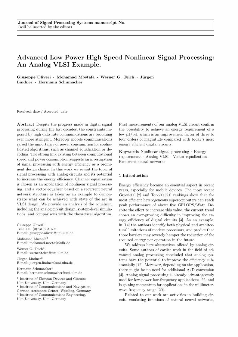
ei
Rst
u k
V ik
Single Neuron(DUT)
'
' Equivalent load
Bufferui'
Fig. 15 Single neuron characterization: realized test struc-ture, including the single neuron (cf. Fig. 3), an equivalentload and additional buffers to facilitate the measurements.The inner state u′k is accessible and used to generate thefeedbacks for the ith neuron.
9 Measurement Results
Our first measurements focused on the functional vali-
dation of the single neuron for real-valued equalizations:
weighted multiplication, β of the activation function,
and cutoff frequency, i.e. the equivalent time constant
τ . For this purpose the circuit of Fig. 15 was realized
using a 250 nm SiGe BiCMOS fabrication process by
IHP. The test structure was bonded and mounted on a
Rogers RO4003 printed circuit board (PCB).
The feedback states u′k for the ith neuron, com-
ing from the other neurons (k ∈ [1, ..., N ], k 6= i), are
here externally generated and directly applied. Pro-
vided that the neuron under test also drives an identical
load (N −1 transconductance stages) as in the full vec-
tor equalizer, the characterization of this elementary
cell remains valid at system level.
Fig. 16 shows the gain variation wik as a function
of the voltage Vik applied. The values are computed by
applying a sinusoidal excitation to u′k and by measuringmagnitude and phase of u′i before the corner frequency
given by τ , at a frequency of 0.1 GHz. The attenuator
– cf. Fig. 4 and 5 – allows the weights to be fine-tuned,
within a span of 1.2 V. The measured curve presents
a shift ∆Vik ≈ 0.1 V with respect to simulations. This
shift can however be easily calibrated in the measure-
ment setup and has not any impact on neuron’s perfor-
mance.
The slope of the activation function β at the ori-
gin – cf. Eqs. (2) and (5) – is a free parameter that
can be optimized. From our simulations, the condition
to fulfill for best performance is β ≥ 3 V-1. Measure-
ments performed at 0.1 GHz resulted in a value of 3.47,
slightly smaller than the simulated one β = 3.87 V-1.
Reasons can probably be imputed to small losses in the
measurement setup.
The equivalent τ for time scaling can be measured
by applying a sinusoidal excitation to the external input
e′i and measuring the frequency response at the neuron
output u′i. Fig. 17 (a) shows the simulated transfer func-
Vik [V]0.8 1 1.2 1.4 1.6 1.8 2
wik
-1
-0.5
0
0.5
1
MeasurementsSimulations
Fig. 16 Voltage mapping wik = f [Vik] ∈ [−1, 1]. Bluesquares represent measured values.
Frequency [GHz]10-1 100 101
|u' i/e
' i| [dB
]
-12
-10
-8
-6
-4
-2
0
Ideal Low-Pass RCCircuit Simulation
(a) |u′i/e′i| frequency response simulation, and comparisonwith an ideal low pass RC filter with τ = 42 ps.
Frequency [GHz]10-1 100 101
|u'(+
)i
/e'(-
)i
| [dB
]
-12
-10
-8
-6
-4
-2
0
SimulationsMeasurements
(b) Single input, single output |u+i /e
+i | frequency response
measurement, and comparison with simulation results.
Fig. 17 Equivalent τ of a single neuron. Measurements con-firm the hypothesis of a first-order low-pass filter comparableto an ideal low-pass RC filter, lumped between u+
i and u−i .
tion |u′i/e′i| and a comparison with an ideal RC low pass
filter with cutoff frequency of 3.79 GHz (τ = 42 ps). The
hypothesis of a frequency response which resembles an
ideal RC behavior is confirmed by Fig. 17 (b), show-
ing the single-input single-output |u+i /e+i |measurement
and the comparison with the expected curve.
Having the single neuron validated by measurement
data, a full vector equalizer has been fabricated (Fig.
18). The chip area of 0.68 mm2 is dominated by the
several pads needed for measurements. The pin config-
uration is the following: four differential external inputs
(pads 1, 2, 3, 4, 5, 6, 7, 8), four differential outputs (pads
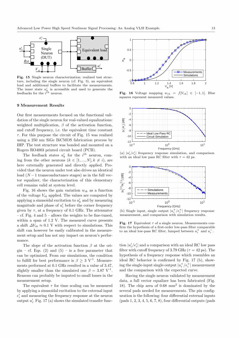
14 Giuseppe Oliveri et al.
GND 1 2 3 4 5 6 7 8 GND
9
10
11
GND 21 19 16 14 GND
23 22 20 18 17 15 13 12
26
25
24
Fig. 18 Layout of the vector equalizer and pin configuration.
9, 10, 11, 12, 23, 24, 25, 26), six pins for the weights con-
figuration (pads 13, 14, 18, 19, 20, 21), reset (pad 15),
voltage supplies (pads 16, 17, 22) and grounds (square
pads). The active area is approximately 0.09 mm2, with
a transistor count CNT = 171 for four neurons. The
power consumption of 35 mW was measured, confirm-
ing simulation results.
A descriptive test to check the functionality of the
equalizer connections is shown in Fig. 19. The equalizer
is tested with a set of input vectors e′ with equal ele-
ments (e′i = e′, i ∈ [1, ..., N ]) and the steady state out-
puts u′ are measured. If the weights are set equally for
all the neruons (wik = w, k ∈ [1, ..., N ], k 6= i), the ex-
pected transfer characteristic u′ = f(e′) complies with
the following transcendental scalar equation:
u′ − w · (Sα) · (N − 1) · tanh
(u′
2 · Vt
)= e′ (24)
The numerical solution of Eq. 24 with w = 1 shows a
hysteresis loop, described by the model in Eq. (25): bnegand bpos are two switching boundaries. When the input
is outside the boundaries, one unique solution exists for
Eq. (24). When the input is within the boundaries, the
output presents two stable solutions. The choice of the
“plus” or “minus” sign in Eq. (25) then depends on the
last crossed boundary. If the input last crossed bpos, the
numerical solution is with the plus sign. Otherwise, the
solution with the “minus” sign is the correct one.
u′ =
e′ + (Sα)(N − 1), ∀ e′ ≥ bpose′ − (Sα)(N − 1), ∀ e′ ≤ bnege′ ± (Sα)(N − 1), ∀ bneg < e′ < bpos
(25)
In other words, because of the neurons’ strong non-
linearities, as the external input increases and reaches
the boundary bpos, the internal state flips from a nega-
tive to a positive value. As the external input decreases
and reaches the boundary bneg, the inner state switches
from a positive to a negative value. The good agreement
between simulations and measurements is confirmed by
External input vector e' [V]-0.8 -0.6 -0.4 -0.2 0 0.2 0.4 0.6 0.8
Inn
er
sta
te v
ecto
r u
' [V
]
-1.5
-1
-0.5
0
0.5
1
1.5b
negb
pos
Fig. 19 Hysteresis curve resulting from a numerical solutionof Eq. (24): comparison between simulations (black line) andmeasured data (blue circles).
Fig. 19, where all the four differential outputs are mea-
sured for each differential external input vector e′.
10 Conclusions
Given the current trend of wireless and mobile commu-
nications, implementing complex algorithms, achieving
high data rates, and at the same time minimizing the
power consumption of a digital signal processing system
is becoming extremely challenging. And the situation is
not likely to be reversed in the near future, by scaling
the minimum feature size of transistors. Our intention is
to turn this challenge into an opportunity to revitalize
the topic of analog signal processing, i.e. implementing
algorithms with efficient dedicated analog circuits.
As an application of analog nonlinear signal process-
ing we presented a vector equalizer for MIMO transmis-
sions, realized in SiGe BiCMOS technology. The equal-
izer can handle vectors of length N = 4 for either BPSK
or QPSK modulation schemes.
Bit error rate performance comparisons showed vir-
tually the same or similar behavior for the common
digital signal processing and the analog VLSI circuit
version. The reason for the comparable robustness –
the input is noisy – is that both types of processing
use equilibrium states of nonlinear dynamical systems
to get the outputs, rather than simple amplitude levels.
The throughput of the vector equalizer is influenced
by the evolution time the analog RNN needs to reach
the equilibrium state. This time in turn depends on
the equivalent time constant τ . In our circuit design
the throughput was maximized by exploiting the low-
pass behavior, given by parasitic capacitances of bipo-
lar transistors and MOSFETs. Furthermore, an on-chip
switch gives the possibility to reset the internal states
of the equalizer – a fundamental prerequisite to handle
a sequence of vectors.
The analog vector equalizer does not need an analog
to digital conversion of the inputs, but needs to be con-

Advanced Low Power High Speed Nonlinear Signal Processing: An Analog VLSI Example. 15
figured with proper weights, representing the channel
state. We showed that the optimum interface requires
a DAC with a minimum resolution of six bits.
The set of measured data confirmed the expected
characteristics of a single neuron. Also the equalizer
was tested with a predefined set of input-output vec-
tors, and always confirmed the simulation results. In
comparison with common digital signal processing we
conclude that the energy efficiency can be improved by
some orders of magnitude. This confirms earlier con-
jectures, stating a huge potential for nonlinear signal
processing with analog circuits.
Acknowledgements Financial support by the German re-search foundation DFG (Deutsche Forschungsgemeinschaft)is gratefully acknowledged. A note of thanks goes also to IHPGmbH for the Si/SiGe foundry processes needed to realizethe circuit.
References
1. Cauwenberghs, G.: An analog VLSI recurrent neural net-work learning a continuous-time trajectory. IEEE Trans-actions on Neural Network 2, 346–361 (1996)
2. CompuGreen-LLC: The green500 list (2015). URLhttp://www.green500.org [Accessed on December 2015]
3. Degnan, B., Marr, B., Hasler, J.: Assessing trends inperformance per watt for signal processing applications.IEEE Transactions on Very Large Scale Integration(VLSI) Systems 24(1), 58–66 (2016)
4. Draghici, S.: Neural networks in analog hardware - de-sign and implementation issues. International Journal ofNeural Systems 10(1), 19–42 (2000)
5. Engelhart, A.: Vector detection techniques with moder-ate complexity. Ph.D. thesis, Ulm University, Instituteof Information Technology (2003)
6. Engelhart, A., Teich, W.G., Lindner, J., Jeney, G., Imre,S., Pap, L.: A survey of multiuser/multisubchannel detec-tion schemes based on recurrent neural networks. Wire-less Communications and Mobile Computing, Special Is-sue on Advances in 3G Wireless Networks 2(3), 269–284(2002)
7. Haykin, S.: Neural networks: A comprehensive founda-tion. Macmillan college publishing company, Inc., USA(1994)
8. Kechriotis, G.I., Manolakos, E.S.: Hopfield neural net-work implementation for optimum CDMA multiuser de-tector. IEEE Transactions on Neural Networks 7(1), 131–141 (1996)
9. Kothapalli, G.: An analogue recurrent neural network fortrajectory learning and other industrial applications. In:3rd IEEE international Conference on Industrial Infor-matics (INDIN), pp. 462–466. Pert, Western Australia(2005)
10. Kuroe, Y., Hashimoto, N., Mori, T.: On energy functionfor complex-valued neural networks and its applications.In: Proc. of the 9th international conference on neuralinformation processing ICONIP’02, vol. 3, pp. 1079–1083(2002)
11. Lindner, J.: MC-CDMA in the context of general mul-tiuser/ multisubchannel transmission methods. Euro-pean Transactions on Telecommunications 10(4), 351–367 (1999)
12. Loeliger, H.A.: Decoding in analog VLSI. IEEE Commu-nications Magazine 37(4), 99–101 (1999)
13. Markram, H.: The human brain project - a report to theeuropean commission. Tech. rep., The HBP-PS Consor-tium (2012)
14. Marr, B., Degnan, B., Hasler, P., Anderson, D.: Scalingenergy per operation via an asynchronous pipeline. IEEETransactions on Very Large Scale Integration (VLSI) Sys-tems 21(1), 147–151 (2013)
15. Mead, C.: Analog VLSI and neural systems. Addison-Wesley (1989)
16. Miyajima, T., Hasegawa, T., Haneishi, M.: On the mul-tiuser detection using a neural network in code-divisionmultiple-access communications. IEICE Trans. on Com-munications E76-B, 961–968 (1993)
17. Mostafa, M.: Equalization and decoding: a continuous-time dynamical approach. Ph.D. thesis, Ulm University,Institute of Communications Engineering (2014)
18. Mostafa, M., Teich, W.G., Lindner, J.: Vector equaliza-tion based on continuous-time recurrent neural networks.In: 6th IEEE International Conference on Signal Process-ing and Communication Systems, pp. 1–7. Gold Coast,Australia (2012)
19. Mostafa, M., Teich, W.G., Lindner, J.: Approximationof activation functions for vector equalization based onrecurrent neural networks. In: 6th International Sympo-sium on Turbo Codes and Iterative Information Process-ing, pp. 52–56. Bremen, Germany (2014)
20. Parlak, M., Matsuo, M., Buckwalter, J.F.: Analog signalprocessing for pulse compression radar in 90-nm CMOS.IEEE Transactions on Microwave Theory and Techniques60(12), 3810–3822 (2012)
21. Prometheus-GmbH: Top500 list (2015). URLhttp://www.top500.org [Accessed on December 2015]
22. Schlottmann, C.R., Hasler, J.: High-level modeling ofanalog computational elements for signal processing ap-plications. IEEE Transactions on Very Large Scale Inte-gration (VLSI) Systems 22(9), 1945–1953 (2014)
23. Teich, W.G., Engelhart, A., Schlecker, W., Gessler, R.,Pfleiderer, H.J.: Towards an efficient hardware imple-mentation of recurrent neural network based multiuserdetection. In: IEEE 6th International Symposium onSpread Spectrum Techniques and Applications, pp. 662–665. NJIT, New Jersey, USA (2000)
24. Teich, W.G., Seidl, M.: Code division multiple accesscommunications: multiuser detection based on a recur-rent neural network structure. IEEE 4th InternationalSymposium on Spread Spectrum Techniques and Appli-cations 3, 979 – 984 (1996)
Giuseppe Oliveri received his
Bachelor and Master degrees in
Electronics Engineering at the Uni-
versity of Palermo, Italy, in 2007
and 2010, respectively. In January
2011 he joined the Electron De-
vices and Circuits Group at the
University of Ulm, Germany, as a
doctoral candidate. His research is
mainly focused on signal process-
ing algorithms, realized with analog circuits. His inter-
ests extend to high frequency microsystems and mono-
lithic microwave integrated circuits, among others.

16 Giuseppe Oliveri et al.
Mohamad Mostafa received
the BEng and Diploma degrees
in Electronics Engineering from
Aleppo University, Syria in 2004
and 2006, respectively and PhD de-
gree in Communications Engineer-
ing from the University of Ulm,
Germany in 2014. Since 2013 he is
a senior research assistant at the
German Aerospace Center (DLR).
His research interests include phys-
ical layer design, dynamical systems and artificial neu-
ral networks, among others.
Werner G. Teich graduated
with a M.Sc. in Physics from
Oregon State University, Corvallis,
Oregon, in 1984. He received the
Dipl.-Phys. and the Dr. rer. nat.
degree in Physics from the Univer-
sity of Stuttgart in 1985 and 1989,
respectively. In 1991 he joined the
Department of Information Tech-
nology, Ulm University, Germany.
Currently, he is Senior Lecturer in Digital Communica-
tions at the Institute of Communications Engineering,
Ulm University. His research interests are in the gen-
eral field of digital communications. Specific areas of
interest include the application of iterative methods in
wireless communications.
Jurgen Lindner is Professor
Emeritus and former head of the
Institute of Communication Engi-
neering at Ulm University. He re-
ceived the Dipl.-Ing. and Dr.-Ing.
degrees in Electrical Engineering
from RWTH Aachen University in
1972 and 1977, respectively. After
some years in industrial research
he was appointed Full Professor at
Ulm University with a chair in Communications En-
gineering in 1991. His research interests are in wireless
digital communications, including broadcast, mobile in-
door and outdoor communications. One special field of
his research interest is the application of artificial neu-
ral networks for low power signal processing with analog
VLSI.
Hermann Schumacher ob-
tained his doctorate in engineering
from RWTH Aachen University in
1986. He was a member of tech-
nical staff at Bellcore, Red Bank,
NJ, USA from 1986 until 1990.
Since 1990, he has been a Professor
with Ulm University. Since 2010,
he is the director of the Institute
of Electron Devices and Circuits,
and since 2011 director of the University’ School of Ad-
vanced Professional Studies. His research areas are in
monolithic IC design for millimeter-wave applications,
and high speed analog signal processing, applied to both
communications and sensor systems.


![ECE-V-DIGITAL SIGNAL PROCESSING [10EC52] …vtusolution.in/.../digital-signal-processing-10ec52.pdfDigital vtusolution.in Signal Processing 10EC52 TEXT BOOK: 1. DIGITAL SIGNAL PROCESSING](https://static.fdocuments.in/doc/165x107/5afe42bb7f8b9a256b8ccd2e/ece-v-digital-signal-processing-10ec52-signal-processing-10ec52-text-book.jpg)