Advanced LIGO UK June 2006
13
LASER INTERFEROMETER GRAVITATIONAL WAVE OBSERVATORY LIGO Laboratory / LIGO Scientific Collaboration Advanced LIGO UK June 2006 Electrostatic Driver Electronics Preliminary Design Document & Test Report N.A. Lockerbie Distribution of this document: Inform aligo_sus This is an internal working note of the Advanced LIGO Project, prepared by members of the UK team. Institute for Gravitational Research University of Glasgow Phone +44 (0) 141 330 5884 Fax +44 (0) 141 330 6833 E-mail [email protected] School of Physics and Astronomy University of Birmingham Phone +44 (0) 121 414 6447 Fax +44 (0) 121 414 3722 E-mail [email protected] Engineering Department CCLRC Rutherford Appleton Laboratory Phone +44 (0) 1235 445 297 Fax +44 (0) 1235 445 843 E-mail [email protected] Department of Physics University of Strathclyde Phone +44 (0) 1411 548 3360 Fax +44 (0) 141 552 2891 E-mail [email protected] http://www.ligo.caltech.edu/ http://www.physics.gla.ac.uk/igr/sus/ http://www.sr.bham.ac.uk/research/gravity/rh,d,2.html http://www.eng-external.rl.ac.uk/advligo/papers_public/ALUK_Homepage.htm
Transcript of Advanced LIGO UK June 2006

LASER INTERFEROMETER GRAVITATIONAL WAVE OBSERVATORY
LIGO Laboratory / LIGO Scientific Collaboration
Advanced LIGO UK June 2006
Electrostatic Driver Electronics Preliminary Design Document & Test Report
N.A. Lockerbie
Distribution of this document:
Inform aligo_sus
This is an internal working note of the Advanced LIGO Project, prepared by members of the UK team.
Institute for Gravitational Research
University of Glasgow Phone +44 (0) 141 330 5884 Fax +44 (0) 141 330 6833
E-mail [email protected]
School of Physics and Astronomy University of Birmingham Phone +44 (0) 121 414 6447 Fax +44 (0) 121 414 3722
E-mail [email protected] Engineering Department
CCLRC Rutherford Appleton Laboratory Phone +44 (0) 1235 445 297 Fax +44 (0) 1235 445 843
E-mail [email protected]
Department of Physics University of Strathclyde
Phone +44 (0) 1411 548 3360 Fax +44 (0) 141 552 2891
E-mail [email protected]
http://www.ligo.caltech.edu/
http://www.physics.gla.ac.uk/igr/sus/
http://www.sr.bham.ac.uk/research/gravity/rh,d,2.html
http://www.eng-external.rl.ac.uk/advligo/papers_public/ALUK_Homepage.htm

Advanced LIGO UK
1 Introduction and scope
1.1 Purpose
This document covers the ongoing development, and the current assessment, of high voltage Electrostatic Drive (ESD) amplifiers intended for the noise prototype tests of quad suspensions for Advanced LIGO. It follows on from document LIGO-T0500110-00-K.
1.2 Contents
•
•
- -
•
- - - -
•
- -
Design philosophy
Circuit diagrams
High Voltage (HV) amplifier
Preamplifier (instrumentation amplifier inputs)
Operation
ESD HV amplifier performance: full-power bandwidth
ESD HV amplifier performance: noise
Preamplifier performance: noise
Thermal issues
System Overview
Over-temperature sensing
Power-rail sequencing
1.3 Reference Documents
[1] LIGO-T0500110-00-K: Electrostatic Drive Amplifier for noise prototype tests
[2] LIGO-E040109-00-K: Electrostatic drive amplifier for controls prototype tests.
[3] LIGO-E040379-01-K: Electrostatic Actuator Drive Electronics Interface Control Document.
[4] LIGO-E050075-00-K: Advanced LIGO electrostatic drive voltage and noise issues.
[5] Apex PA94 data sheet is available on: http://eportal.apexmicrotech.com/mainsite/pdf/pa94u.pdf
[6] “Composite Amplifier has Low Noise and Drift”, Electronic Design, 12 June, 2000, by Paul Brokaw (Analog Devices).
[7] GEO-T050263-00-K: Electrostatic drive (ESD) results from GEO.
[8] LIGO-T060084-00-K: Water-cooling System for the Electrostatic Drive Amplifier.
2

Advanced LIGO UK
2 Design Philosophy This work follows on from that carried out with the electrostatic drive amplifier used in the initial noise prototype tests, as detailed in document LIGO-T0500110-00-K. The amplifier’s design therefore draws on the conclusions reached by K. Stain, as detailed in document LIGO-E050075-00-K: that is, that greater flexibility and control accuracy in steering the suspended mirrors using electrostatic control would be afforded by moving to
(i) two counter-electrodes for each quadrant array of electrodes patterned on the reaction masses, one strongly-coupled to the quadrant electrodes, and one weakly-coupled; and
(ii) a two-level drive output from the electrostatic driver electronics for each electrode, via paired controlling DACs. One DAC output could then provide coarse control, the other fine control, of the mirror.
(iii) Both (i) and (ii) would individually have the effect of greatly increasing the dynamic range of the electrostatic control—needed because of the dual requirements for the ESD: to provide short term peaks of feedback force for acquisition, and to provide continuous high frequency (above 1 Hz) feedback in science mode.
Therefore, the baseline for this work was an electrostatic amplifier having 6 output channels, in order to accommodate the additional weakly-coupled counter electrode. In addition, each ESD channel would now have two control inputs: a ‘Hi’ level input for coarse control, and a ‘Lo’ level input for fine control, such that both could be applied simultaneously via the single high-voltage output from that channel.
It was decided to split the function of each ESD channel between two PCBs: two low-voltage Preamplifiers to carry out signal conditioning functions for the Lo and Hi inputs, and a High Voltage PCB to carry a PA94 power amplifier and its associated circuitry.
As the distance between each mirror and reaction mass may be ~5 mm in Advanced LIGO, as compared with 3 mm in GEO 600, a high value of ±400 volts was assumed for the eventual target working output for each ESD channel. This implies supply voltages of ±430 V, since in practice up to ±30 V may be lost across the PA94 (±450 V are the maximum allowed supply voltages for the PA94 devices, ±50 V being the minimum).
At the time of writing the question of the required bandwidth for each ESD channel is still unresolved. It is clear that it will have to operate from DC up to (possibly) several hundred Hz, but operation at up to 16 kHz has not yet been ruled out. For this reason the PA94 amplifier has been retained, for the time being. However, if the ESD ultimately has to operate only below (a few) hundreds of Hz, say, then PA95 amplifiers ought to be used in place of the PA94s, with the benefit of an order of magnitude reduction in their static thermal dissipation. Dynamic or short-circuit dissipation would be unchanged, however.
3

Advanced LIGO UK
3 Circuit Diagrams
3.1 High Voltage (HV) amplifier
A significant problem encountered originally with the PA94-based high voltage amplifier circuit was stability. This was overcome by using a composite amplifier in which the PA94 was placed inside the feedback loop of a low-voltage, low-noise, OP 27 operational amplifier [6]. The latest version of the resulting circuit (ver. 2) is shown in Fig.1. One significant change from the ver. 1
Figure 1. ESD High Voltage driver circuit, ver. 2. This PA94-based circuit differs from ver.1 only in having an auxiliary ‘HV Monitor’ output, and a ×4 (rather than ×0.4) Lo level gain. The Lo level input to the preamplifier (±10 V) provides a gain of ×4 overall, i.e. ±40 V at the HV output, whilst the Hi level input to the preamplifier (also ±10 V) provides a gain of ×40, i.e. ±400 V at the output. These effects are summed at the HV output. A low-voltage ‘HV Monitor’ output (±10 V Monitor output for a ±400 V HV channel output) is also available.
circuit is the way in which the Hi and Lo inputs from the preamplifier interfaces are summed. Here, the input resistors are simply in the ratio 10:1 (leading to a signal weighting at the HV amplifier’s output of 10:1, rather than the 100:1 of the ver.1 circuit), giving a noise gain of 45 for the circuit, rather than 81, as in the ver.1 circuit—and without a concomitant increase in Johnson
4

Advanced LIGO UK
Figure 2. The ESD driver differential Monitor output circuit for one ESD channel: a ±10 V analog of the ±400 V output from each HV channel is available here both buffered, and buffered and inverted, at the two Monitor outputs. A seventh identical differential circuit can provide a water flow-rate monitor output, taking as its input the 0–10 V flow-rate signal (TBD). Each LT1124 op-amp is powered by ±15 V supply rails, decoupled at each IC with 10µ Tantalum bead and 0.1µ ceramic capacitors.
noise. This circuit also incorporates a low-voltage Monitor output, which allows the actual HV output to be monitored remotely via a ±10 V analog signal. Figure 2 shows the differential output Monitor interface circuit.
3.2 Preamplifier (instrumentation amplifier inputs)
Off-the shelf instrumentation amplifier ‘front-ends’ were found to be optimized from the noise point of view for high gain, where very low-value (tens of Ohms) external gain-determining resistors ‘shorted-out’ their noise. Unfortunately, these same amplifiers yielded noise Power Spectral Densities of well over 100 nV/ Hz at 1 Hz when used at unity gain. Unity gain is needed in this application, and so a discrete low-noise front-end was designed and built around a low noise dual op-amp IC package (for low drift), followed by a low-noise single op-amp. This arrangement is used for both the Hi and Lo inputs to each channel. The circuit is shown in Fig.3. Johnson noise has been kept low in this circuit by using resistors typically a factor of 15–20 smaller than those used in off-the-shelf instrumentation amplifiers, whilst simultaneously minimizing the current and voltage noise sources due to the op-amps themselves. At present the unmodified bandwidth of the Preamplifier extends down to DC, and at the top end largely exceeds that of the HV amplifier (at 105 kHz).
5

Advanced LIGO UK
Figure 3. The ES Driver Preamplifier circuit for one ESD channel, buffering both the Hi (×40) and Lo (×4) differential inputs. The function of the rightmost (inverting) amplifier for each input is to tailor the bandwidth of the Preamplifier (TBD). This circuit was configured for comparative noise tests.
4 Operation
4.1 ESD HV amplifier performance: full power bandwidth
Figure 4. Frequency response of the PA94-based ESD High Voltage driver circuit, ver.1, using ±307 V supply rails, and with a 576 V p-p output below 20 kHz. The gain of ×40 extended down to DC. The frequency response was not plotted beyond 35 kHz when connected to the 1300 pF load, because the peak output current then exceeded the 70 mA current-limit set for the PA94 amplifier.
6

Advanced LIGO UK
Version 1 of this circuit was found to have a large phase margin, and to exhibit excellent stability—even with a 560 V p-p 1 kHz square-wave output. Its -3 dB bandwidth was found to extend from DC to 105 kHz, as shown in Fig.4. Its large signal square-wave performance is shown in Fig.5.
Figure 5. Large-signal response of the ES Driver’s High Voltage output: a 14 V p-p, 1 kHz, square-wave was applied to the Hi (×40) input. The output is seen to be 560 V p-p, as expected, with no evidence of overshoot or ringing.
7

Advanced LIGO UK
4.2 ESD HV amplifier performance: noise Table 1. Noise performance of the ES Driver’s HV circuit ver.1, using three different ancillary op-amps. Here, the noise is referred to the input of the HV amplifier, whose noise gain was 81. Although the AD 743 had a significantly poorer noise and offset performance for frequencies at and below 1 Hz than the OP 27E, its high frequency (> 20 kHz) large signal performance was better, producing less signal offset through anomalous rectification.
Power Spectral Density (nV/ Hz ) @
Frequency (Hz): 1 10 48.5 100 1000 4096 8192 16384 32768 DC offset
(mV)
PA94 + OP 27E 14.9 6.7 6.8 5.7 5.5 5.9 6.1 6.5 6.6 -0.08
PA94 + AD 743 27.8 7.8 6.4 6.6 5.2 5.9 5.9 6.2 6.4 20.2
PA94 + OP 07 12.8 12.6 11.8 11.6 1.8
The noise performance of the ES Driver’s HV circuit ver.1 is shown in Table 1. It is anticipated that the performance of ver. 2 of the circuit will be very similar—perhaps even marginally lower—in noise. However, the overall noise performance of the ES Driver is dominated by that of the preamplifier.
4.3 Preamplifier performance: noise
The measured preamplifier noise is shown in Fig.6. At a frequency of 1 Hz it is seen to be approximately double that of the HV amplifier (34 nV/ Hz , cf 15 nV/ Hz ), whilst at 10 Hz the ratio is nearly three (20 nV/ Hz , cf 6.7 nV/ Hz ). Of course a major difference between these two elements of the ES Driver is that the composite HV amplifier acts effectively as a single op-amp, with a single fairly low-value (2k22) input resistor, whereas the Preamplifier acts as four independent op-amps, the ensemble being furnished with eight fairly low value (2k) resistors.
8

Advanced LIGO UK
Figure 6. Blue curve: noise performance of the ‘instrumentation amp’ Preamplifier when followed by a single OP 27-based stage with a gain of -200. Black curve: noise performance of the OP 27 stage alone. In both cases the measured noise level has been referred to the input of the OP 27. Thus the noise PSD of the Preamplifier’s instrumentation amplifier front-end alone was found to be 31 nV/ Hz at 1 Hz, and
18 nV/ Hz at 10 Hz.
4.4 Thermal issues. The ESD is currently designed around the PA94 (or pin-for-pin compatible PA95) high voltage power amplifier, from Apex. Microtechnology. Using the highest voltage power rails available locally for the ESD (±307 V), and under no-load conditions, the static power dissipated in the ESD’s PA94 amplifier has been measured to be 10.1 W. For operation using the projected ±430 V power rails—which would enable an output signal to be generated by the ESD in the range ±400 V (the design target)—this static dissipation would rise to 14.7 W for each PA94. Using PA95 amplifiers in place of PA94s, would reduce this static dissipation by an order of magnitude, albeit at the loss of high frequency (>20 kHz) performance. Additional AC-, or indeed short-circuit-, dissipation would be the same in both devices, however. For the target maximum ESD output of 800 Vp-p, at 16.384 kHz, say, using the ±430 V supply rails mentioned above, and with a 1300 pF load (which would give a peak current of 54.1 mA), the predicted dissipation rises to 30.1 W (PA94), or 16.9 W (PA95). It is noteworthy that with the current-limit of the PA94 (or PA95) set to the anticipated value of 70 mA, the power dissipated in the PA94/5 under short-circuit output conditions would be 28 W in addition to the static dissipation—i.e., approximately 42.5 W for the PA94, or 29.5 W for the PA95. As this is a condition that could conceivably occur by mischance during practical operation, it was felt that active cooling of the PA94/5 amplifiers would be beneficial from the point of view of safety—even if AC operation of the ESD at frequencies as
9

Advanced LIGO UK
high as 16 kHz were not to be envisaged. Rupture of the PA94/5 packaging under excessive dissipation certainly should be avoided.
Therefore, it was felt that a cooling system would be needed that would be capable of coping with potentially up to ~ 40 W per PA94/5, whilst maintaining the PA94/5 at a safe operating temperature. Earlier work detailed in [1] used fan-cooled heatsinks, which were shown to function quite satisfactorily at a total dissipation of ~ 40 W per heatsink. These would almost certainly have functioned adequately well under double this dissipation, with two PA94/95 devices per heatsink, each dissipating ~ 40 W. Unfortunately, fan-cooled heatsinks are unsuitable for the cooling of electronics in Advanced LIGO, because of the level of acoustic noise the fans generate, the level of electromagnetic interference they create, and the frequency spectrum over which these effects are produced. It was therefore proposed to investigate water-cooling of the heatsinks. Clearly, this can be a very low noise option from an acoustical point of view, particularly as the water flow-rates that are required turn out to be very modest. Electromagnetic interference can also be reduced to negligible levels with this type of cooling, although some kind of water flow-rate sensor and flow-rate front-panel analog display has been found to be essential. The water-cooled heatsinks and flow-rate monitor/display are described in [8]. The water flow-rate monitor uses a pelton-wheel sensor that chops an internal infrared beam, and so generates no magnetic interference. It gives a 0–10 volt output for 0–1 litre/minute water flow-rate.
Figure 7. Three water-cooled heatsinks sized to fit into a 19″ 3U rack-mounting cabinet. Each heatsink can carry two 6″× 4″ PCBs. The heatsinks are cooled by water flowing through flexible 4 mm o.d. nylon tubing interconnections. Each heatsink can be re-orientated by ±90º about a horizontal axis, so as to give easy access from above to either of its two PCBs. The figure shows six dummy loads connected to the nominally 250 V AC (245 V, actual) mains supply, each load dissipating 40 W. A very modest flow rate of 0.5 litres/minute provided 240 W of cooling power for a 7 ºC rise in water temperature from inlet to outlet.
10

Advanced LIGO UK
5 System overview The complete 19″ (possibly 6U: TBD) rack-mounting 6-channel ES Driver system is shown in block diagram form in Fig.8. The single-ended ±400 V channel outputs are to be routed via front-panel mounting SHV connectors. The Hi and Lo channel inputs, and the differential HV Monitor and water flow-rate outputs, are to be routed via D-sub connectors on the front panel, as are the 5 volt digital signals comprising 6 × over-temperature alarms (normally high), and one ‘cooling water flow-rate too-low’ alarm (normally high)—TBD.
Figure 8. Block diagram of the 6-channel ES Driver. Each of the channels, labeled 0–5, has two ±10 V differential inputs labeled Hi (×40) and Lo (×4), a single High Voltage output (±400 V), and a low voltage Monitor output (differential: ±10 V). A cooling-water flow-rate monitor also can have a differential monitored output (TBD), as well as a digital output that will switch low if the water flow-rate drops below a preset level. In addition, each PA94/5 power amplifier has a thermal sensor attached to its cooling tab that will cause a digital output to switch low if the device overheats (i.e., the tab rises above 50ºC, say).
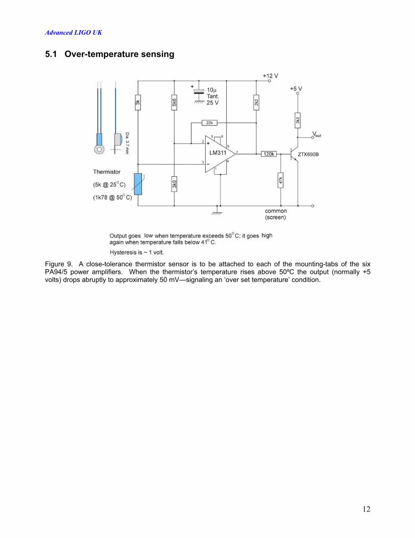
Over-temperature monitoring of the PA94/5 devices is carried out with surface-mount thermometer circuits 15 mm × 30 mm (double-sided, with the outer side grounded—as an electrostatic screen) attached locally to the cooling tab of each PA94/5. The circuit is shown in Fig.9.
The power-rail sequencing logical diagram is shown in Fig.10.
11
Advanced LIGO UK
5.1 Over-temperature sensing
Figure 9. A close-tolerance thermistor sensor is to be attached to each of the mounting-tabs of the six PA94/5 power amplifiers. When the thermistor’s temperature rises above 50ºC the output (normally +5 volts) drops abruptly to approximately 50 mV—signaling an ‘over set temperature’ condition.
12

Advanced LIGO UK
13
5.2 Power-rail sequencing
Figure 10. ESD driver power-rail sequencing schematic. The ±430 V rails are only routed to the ES Driver HV circuitry if (i) they are both present at the input, and (ii) the ±15 V rails are also present, and (iii) the Start/Reset switch has been pressed on the front panel of the ES Driver. Relay sequencing allows a soft-start for the ±430 V rails. If any of the four power rails is removed even temporarily, once the ES Driver has been powered-up, then all four rails are removed automatically—the ±430 V rails being forced to collapse first by discharging through dummy loads. The circuitry then latches all four rails OFF (its default condition) until power has been restored to all of the rails and the Start/Reset switch has been pressed once again—for reasons of safety