
Antimonide-based compound semiconductors for electronic devices: A

~ 11111111111 ~ijrlrllll[llfll~rl~il]rllrll[~rl~ 11111111111
, -
3 117600501 5988 I
NASA Contractor Report No. 165799
Advanced Indium Antimonide Monolithic Charge Coupled Infrared Imaging Arrays
NASA-CR-165799
T.L. KOCH, C.A. MERILAINEN, (cr~2 000 S4 S3
r- and R.D. THOM
SANTA BARBARA RESEARCH CENTER Goleta, CA 93117
CONTRACT NAS1-16383 NOVEMBER 1981
NI\S/\ National Aeronautics and Space Administration
Langley Research Center Hampton, VlrQlnla 23665
https://ntrs.nasa.gov/search.jsp?R=19820005483 2018-05-28T15:30:01+00:00Z

NASA CONTRACTOR REPORT 165799
ADVANCED INDIUM ANTIMONIDE (InSb)
MONOLITHIC CHARGE COUPLED INFRARED
IMAGING ARRAYS
T.L. Koch, C.A. Merilainen and R.D. Thom
Santa Barbara Research Center 75 Coromar Drive
Goleta, California 93117
November 1981
FINAL REPORT
Contract No. NASl-16383
Prepared -for
National Aeronautics and Space Administration Langley Research Center Hampton, Virginia 23665

This Page Intentionally left Blank

FOREWORD
This Final Report was prepared by Santa Barbara Research Center, Goleta,
California, under Contract No. NASl-l6383. The technical effort was performed
during the period of 10 September 1980 to 10 June 1981. The work was sponsored
by the Langley Research Center, National Aeronautics and Space Administration.
The Technical Representative for NASA was William E. Miller. The Program Mana
ger was Richard D. Thom; the Project Engineer was Thomas L. Koch.
iii
(THIS PAGE INTENTIONALLY LEFT BLANK)
iv
Section
1
2
3
4
5
6
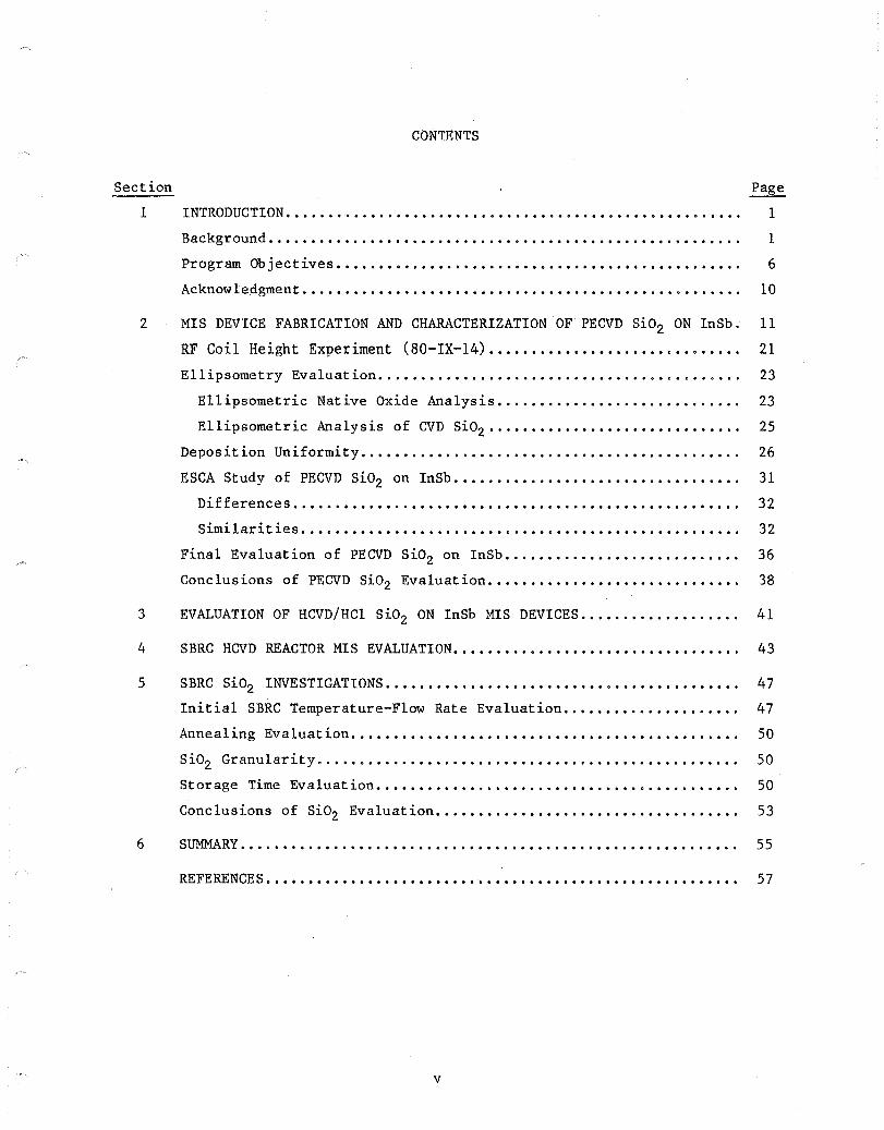
CONTENTS
INTRODUCTION.
Background •.•
Program Objectives.
Acknowledgment ••••••
MIS DEVICE FABRICATION AND CHARACTERIZATION OF PECVD Si02 RF Coil Height Experiment (80-lX-14) •••••••
Ellipsometry Evaluation ••
Ellipsometric Native Oxide Analysis •••.
Ellipsometric Analysis of CVD Si02 •.•••
Deposition Uniformity ••••••.•.••••••
ESCA Study of PECVD Si02 on lnSb.
Differences •••
ON InSb.
Page
1
1
6
10
11
21
23
23
25
26
31
32
Similarities. . .................. 0........................... 32
Final Evaluation of PECVD Si02 on InSb •••••••••.••••••••••••••.••. 36
Conclusions of PECVD Si02 Evaluation.............................. 38
EVALUATION OF HCVD/HCl Si02 ON InSb MIS DEVICES ..•••••.••.•••••...
SBRC HCVD REACTOR MIS EVALUATION •••••••••••••••••••••••••••••••••.
SBRC Si02 INVESTIGATIONS ••••.•••••••.•.•••••••••
Initial SBRC Temperature-Flow Rate Evaluation •••
Annealing Evaluation.
Si02 Granularity •.•••
Storage Time Evaluation •••••••..
Conclusions of Si02 Evaluation •.
S lJr-1M.ARY CI • • • • • • • • • • • • • • • • • • • • • • • • • • • • •
REFERENCES •.••••••••••••••••••••••••.
v
41
43
47
47
50
50
50
53
55
57
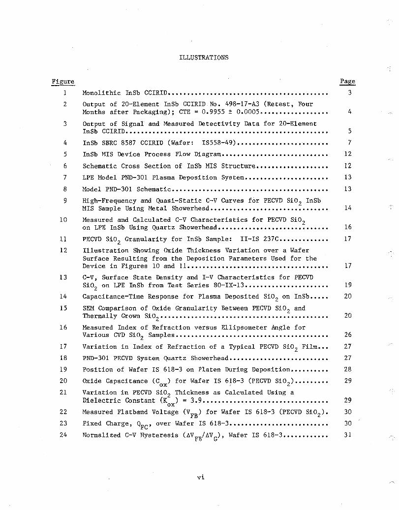
Figure
1
2
3
4
5
6
7
8
9
10
11
ILLUSTRATIONS
Monolithic InSb CCIRID ••••••••••••••••••••••••••••••••••••••• o ••
Output of 20-Element InSb CCIRID No. 498-17-A3 (Retest, Four Months after Packaging); CTE = 0.9955 ± 0.0005 ••••••••••••••••••
Output of Signal and Measured Detectivity Data for 20-Element lnSb CCIRID •••••••••••••••••••••••••••••••••••••••••••••••••••••
InSb SBRC 8587 CCIRID (Wafer: IS558-49) ••••••••••••••••••••••••
InSb MIS Device Process Flow Diagram ••••••••••••••••••••••••••••
Schematic Cross Section of InSb MIS Structure •••••••••••••••••••
LPE Model PND-301 Plasma Deposition System ••••••••••••••••••••••
Model PND-301 Schematic •••••••••••••••••••••••••••••••••••••••••
High-Frequency and Quasi-Static C-V Curves for PECVD Si02 InSb MIS Sample Using Metal Showerhead •••••••••••••••••••••••••••••••
Measured and Calculated C-V Characteristics for PECVD Si02 on LPE InSb Using Quartz Showerhead •••••••••••••••••••••••••••••
PECVD Si02 Granularity for InSb Sample: II-IS 237C •••••••••••••
12 Illustration Showing Oxide Thickness Variation over a Wafer Surface Resulting from the Deposition Parameters Used for the
Page
3
4
5
7
12
12
13
13
14
16
17
Device in Figures 10 and 11..................................... 17
13
14
15
C-V, Surface State Density and I-V Characteristics for PECVD Si02 on LPE InSb from Test Series 80-IX-13 ••••••••••••••••••••••
Capacitance-Time Response for Plasma Deposited Si02 on InSb •••••
SEM Comparison of Oxide Granularity Between PECVD Si0 2 and Thermally Grown. Si02 ••••••••• " .••••••••••••••..••..•••••••••••••
19
20
20
16 Measured Index of Refraction versus Ellipsometer Angle for
17
18
19
20
21
22
23
24
Various CVD Si02 Samples........................................ 26
Variation in Index of Refraction of a Typical PECVD Si02 Film •••
PND-301 PECVD System Quartz Showerhead ••••••••••••••••••••••••••
Position of Wafer IS 618-3 on Platen During Deposition ••••••••••
Oxide Capacitance (Cox) for Wafer IS 6~8-3 (PECVD Si02) •••••••••
Variation in PECVD Si02 Thickness as Calculated Using a Dielectric Constant (K ) = 3.9 ••••••••••••••••••••••••••••••••• ox Measured Flatband Voltage (VFB ) for Wafer IS 618-3 (PECVD Si02).
Fixed Charge, QFC' over Wafer IS 618-3 ••••••••••••••••••••••••••
Normalized C-V Hysteresis (~VFB/~VG)' Wafer IS 618-3 ••••••••••••
vi
27
27
28
29
29
30
30
31
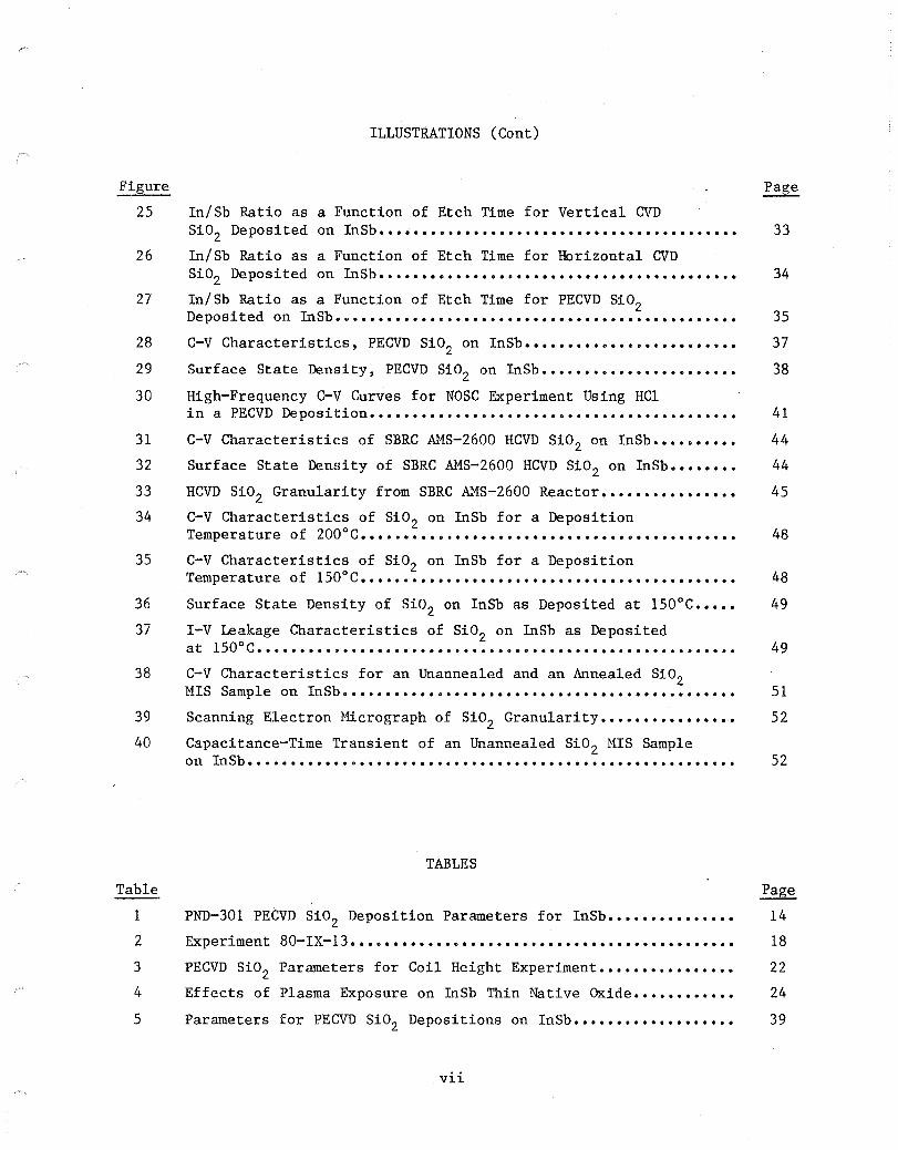
Figure
25
ILLUSTRATIONS (Cont)
In/Sb Ratio as a Function of Etch Time for Vertical CVD Si02 Deposited on rnSb ••••••••••••••••••••••••••••••••••••••••••
26 In/Sb Ratio as a Function of Etch Time for Horizontal CVD
27
28
29
Si02 Deposited on InSb ••••••••••••••••••••••••••••••••••••••••••
In/Sb Ratio as a Function of Etch Time for PECVD Si02 Deposi ted on lnSb 0 ••••••••••••••••••••••••••••••••••••••••••••••
C-V Characteristics, PECVD Si02 on InSb •••••••••••••••••••••••••
Surface State Density, PECVD Si02 on In8b ••••••••••••.•••••••.••
30 High-Frequency C-V Curves for NOSC Experiment Using HCI
33
34
35
37
38
in a PECVD Deposition........................................... 41
31
32
33
34
35
36
37
38
39
40
Table
1
2
3
4
5
C-V Characteristics of SBRC AMS-2600 HCVD Si02 on InSb ••••••••••
Surface State Density of SBRC AMS-2600 HCVD Si02 on InSb ••••••••
HCVD Si02 Granularity from SBRC AMS-2600 Reactor ••••••••••••••••
C-V Characteristics of Si02 on InSb for a Deposition Temperature of ZOO°C ••••••••••••••••••••••••••••••••••••••••••••
C-V Characteristics of Si02 on InSb for a Deposition Temperature of 1500 c ......... 0 ••••••••••• 0 .••••••••••••••••••••••
Surface State Density of Si02 on InSb as Deposited at 150°C •••••
I-V Leakage Characteristics of 8i02 on In8b as Deposited at ISO°C ••••••••••• " ••••••••••••••••••••••••••••••••••••••••••••
C-V Characteristics for an Unannealed and an Annealed 8i02 MIS Sample on InSb •••••••.••••••••••••••.•••••••••••••••••••••••
Scanning Electron Micrograph of 8i02 Granularity ••••••••••••••••
Capacitance-Time Transient of an Unannealed Si02 MIS Sample on rnSb ••.•••••.•••••..•••••••.••••••••••••••••••.•••••.••••.•••
TABLES
PND-301 PECVD Si02 Deposition Parameters for InSb •••••••••••••••
Experiment 80-IX-I3 ••..•..•.•.••........•.....•••.•..•••.....•..
PECVD Si02 Parameters for Coil Height Experiment ••••••••••••••••
Effects of Plasma Exposure on In8b Thin Native Oxide ••••••••••••
Parameters for PECVD Si02 Depositions on InSb ••••••.•••.••••••••
vii
44
44
45
48
48
49
49
51
52
52
Page
14
18
22
24
39
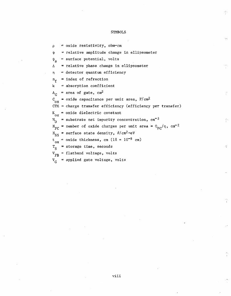
SYMBOLS
= oxide resistivity, ohm-em
relative amplitude change in ellipsometer
surface potential, volts
= relative phase change in ellipsometer
n
nf
= detector quantum efficiency
= index of refraction
k = absorption coefficient
AG = area of gate, cm2
C = oxide capacitance per unit area, F/cm2 ox
CTE = charge transfer efficiency (efficiency per transfer)
K = oxide dielectric constant ox ND substrate net impurity concentration, cm- 3
NFC number of oxide charges per unit area = QFC/ q , cm- 2
NSS = surface state density, #/cm2 -eV
t = oxide thickness, cm (IA = 10-8 cm) ox
TS = storage time, seconds
VFB = flatband voltage, volts
VG = applied gate voltage, volts
viii
Section 1
INTRODUCTION
Future infrared sensors will benefit in reduced weight, volume, and power
requirements of the detector array and associated electronics through the use
of monolithic integrated detector charge-coupled infrared imaging devices
(CCIRIDs). CCIRIDs may be configured in linear or area array configurations
and can be used for either staring or scanning applications. Scanning configu
rations designed to operate in time delay and integration (TDI) modes will
allow a square root in the number of detectors improvement in the detected
signal. Such devices should be capable of operating at high speeds with excel
lent charge transfer efficiencies (CTE) and have on-chip amplifying MISFETs
with high transconductance values.
The long-range objective of this work is to develop a new concept in infra
red imaging sensors utilizing charge transfer techniques. These devices are
intended for use in the infrared spectral range from 1 to 5.4 ~m, and are to be
used for remote sensing of the earth's environment (from spacecraft and/or
aircraft) and other objects in the solar system, e.g., astronomy and planetary
imagl.ng applications, as well as other IR imaging applications.
Indium antimonide (InSb) has been one material of interest for developing
CCIRIDs to meet the 1- to 5.4-~m spectral requirement. Ingots of InSb can be
grown with relatively high purity, low dislocation density, and in sufficient
size to permit wafer diameters in the 2.5- to 4.0-cm range, suitable for con
venient handling and photolithography. It is more tolerant to exposure to
elevated temperatures during processing than other narrow-bandgap materials and
permits diffusion or annealing cycles up to 400°C before surface decomposition
begins to occur.
BACKGROUND
The feasibility of InSb monolithic CCIRIDs has been the intention of devel
opment efforts conducted under NASA funded contracts since 1973. During the
course of these contracts, four generations of CCIRID designs have been gener
ated and several major milestones have been achieved in CCIRID operational
characteristics. An important milestone was achieved under Contract NAS1-13163
with the first successful fabrication and demonstration of charge transfer in
an InSb CCD.l The relatively low CTE of these first devices (0.90) was due to
1
limitations in achievable gate dimensions at that time. This was improved by
dimensional reductions in a second chip design which allowed the CTE to in
crease to 0.975.2
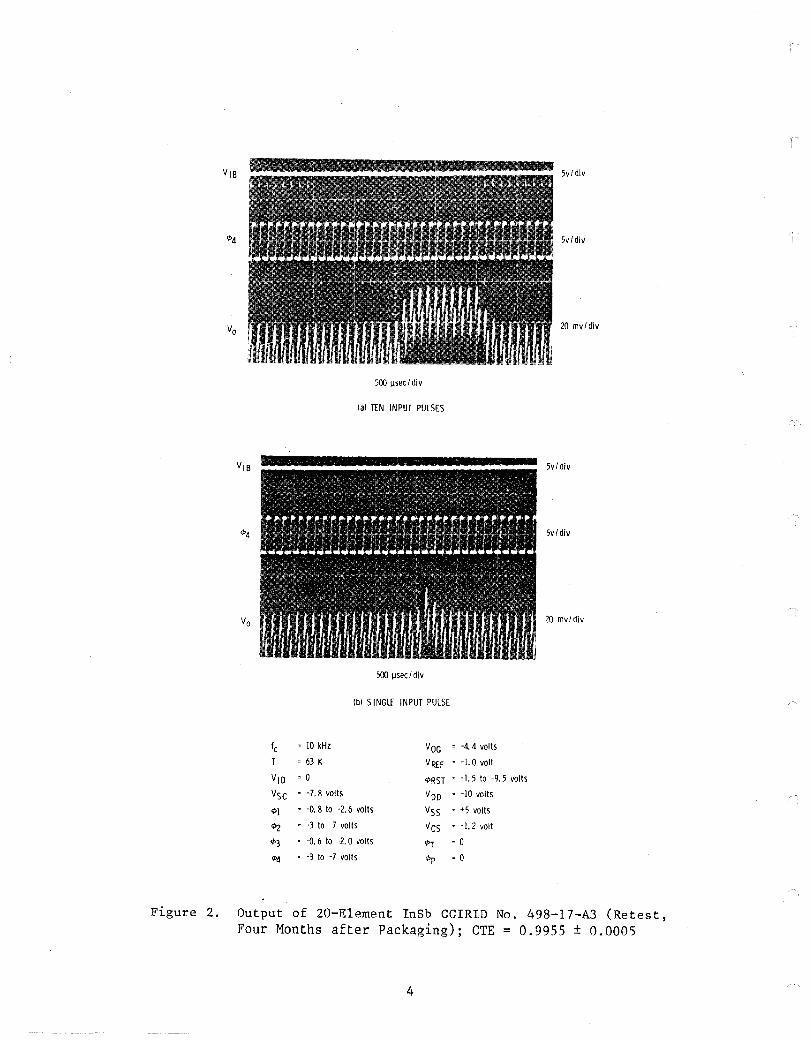
During Contract NASI-I4922, the first monolithic lnSb CCD array, integrat
ing a linear array of 20 MaS detector elements with an lnSb CCD multiplexer,
was achieved. 3 Photomicrographs of 1) an initial and completed SBRC 8585 lnSb
wafer, 2) an overall SBRC 8585 chip, and 3) a 20-element monolithic lnSb CClRlD
array are shown in Figure 1. These devices are typified by CTE values ranging
from ~0.990 to ~0.997. A typical output for one of these devices is shown in
Figure 2.
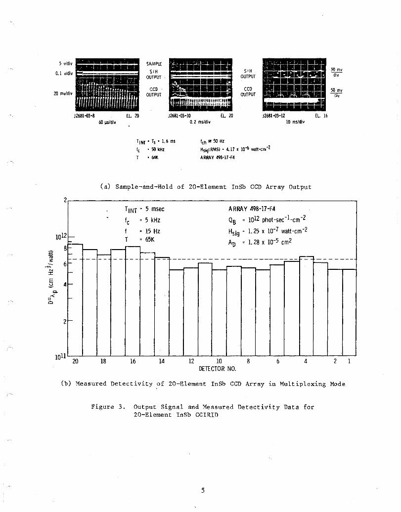
During Contract NASI-I555I the performance characteristics of the 20-ele
ment lnSb CCD arrays were further evaluated and improved operational character
istics were obtained. 4 Detectivity measurements for one array were made using
a clamped sample-and-hold amplifier. Data for this array, clocked in the mul
tiplexing mode, are shown in Figure 3. Under low background conditions, sin
gle-element peak detectivity values exceeding 8xIOll cm-Hz l/2_watt-' and an
array detectivity average of 6.4xIOll cm-Hz l/2_watt- 1 were measured. Other
radiometric characteristics of the lnSb arrays, including quantum efficiency,
linearity and dynamic range, were also evaluated and reported. 5 ,6
Operation of the 20-element lnSb CCD arrays with the transfer gate timing
changed to obtain TDl of the detector signals has also been evaluated. At a
clock frequency of f = 500 Hz and T = 59K, a measured TDl peak detectivity of c
8xI012 cm-Hzl/2-watt-l was achieved.
Evaluation of the detector quantum efficiency (n) was performed, and a
value of n ~ 0.5 measured. This verifies the quantum efficiency advantage of
intrinsic detector materials as compared to monolithic Si:X arrays, for which n
is approximately a factor of two lower. This value was limited by the use of
thin (~75A) titanium photogates in these devices. A replacement structure
using an indium-tin-oxide conductive layer has been developed for which com
puter analysis predicts the photogate structure transmission should increase
from 50 to greater than 70% over the 2.5- to 5.4-~m range. With this improve
ment incorporated, a proportional improvement in quantum efficiency should be
attained.
Two 20-element lnSb devices were delivered to NASA for evaluation in 1978
on Contract NASI-I4922 and two additional arrays with similar characteristics
2
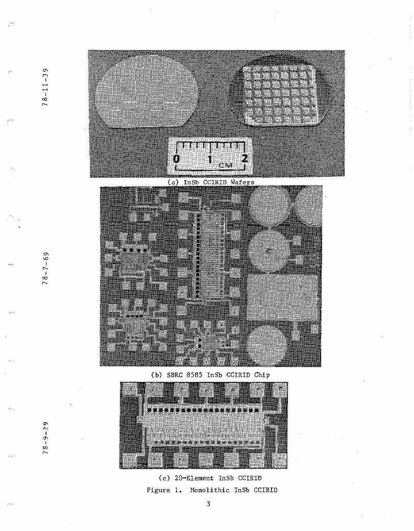
(b) SBRC 8585 InSb CClRlD Chip
(c) 20-Element InSb CClRlD
Figure 1. Monolithic InSb CClRlD
3
V,B 5vl div
5vl div
20 mvldiv
500 Ilsee I div
(al TEN INPUT PULSES
5vl div
5vl div
20 mvldiv
500 Ilsee I div
(bl S INGLE INPUT PULSE
Ie • 10 kHz VOG • -4.4 volts
T • 63 K VREF • -I. 0 volt
V,O • 0 ~RST • -1.5 to -9.5 volts
Vsc • -7.8 volts Voo • -10 volts
~1 • -0.8 to -2.6 volts VSS • +5 volts
~ • -3 to -7 volts Ves • -1.2 volt
¢3 • -0.6 to -2.0 volts ~T • 0 ¢4 • -3 to -7 volts ¢p • 0
Figure 2. Output of 20-Element InSb CCIRID No. 498-17-A3 (Retest, Four Months after Packaging); CTE = 0.9955 ± 0.0005
4
-'"'IN N :r: E ~
5 y/diy '!!!!!!!~ 0.1 y/diy I
20 mv/div
J268Hl3-8 EL 20 60 IIS/div
SAMP\.£
S/H OUTPUT
eeo OUTPUT
J2681-o3-10 EL 20 0.2 ms/div
S/H OUTPUT
eeo OUTPUT
J2681-o3-12 EL. 16 10 ms/div
50 my d1V
50 my dlV
TINT' Ts • 1.6 ms Ich SiI 50 Hz
Ie • 50 kHz
T • 64K
Hsig( RMS) • 4.17 x 10⁻⁶ watt-cm-2
ARRAY 498-17-f4
(a) Sample-and-Hold of 20-Element lnSh CCD Array Output
2~--------------------------------------------------------------~ TINT = 5 msec
fe = 5 kHz
f = 15 Hz T = 65K 1012 1-
F=-81- I--- ~ r---
I-- r---- -- - - - - __ 1- __ �--
6 l-f-
4 ..... -
ARRAY 498-17-:-F4
Os = 1012 phot-sec-Lcm-2
Hsig = 1. 25 X 10-7 watt-cm-2
AD = 1. 28 X 10-5 cm2
----------- -------------~ -------..--- __ ~.--- I---LI _-T""~--' I--- r--- I--....-~
c. -<
~z. ..... Q
2 i-
lOll L-20-L-L-lg-L-L-16-L-L-1-4 ..L----L-1-2..l----L-
1-O ..l----1_
g --L.---I-
6...J-_L-
4 -L----JL--
2-.L...-
1...J
DETECTOR NO.
(b) Measured Detectivity of 20-Element lnSh CCD Array ~n MUltiplexing Mode
Figure 3. Output Signal and Measured Detectivity Data for 20-Element lnSb CClRlD
5
were delivered on Contract NASl-15551. Further evaluation of the deep space
astronomy applications for these devices is being conducted by operating one of
the originally delivered 20-element imagers in the Space Infrared Telescope
Facility (SIRTF) under a joint Langley Research Center and Ames Research Center
program. Finally, a prototype imaging facility is being assembled at Langley
Research Center to demonstrate the utility and capability of these devices to
potential users.
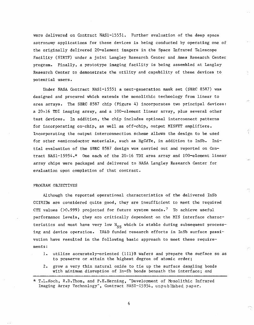
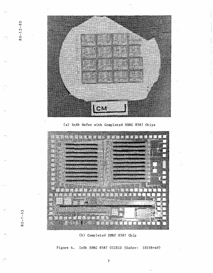
Under NASA Contract NASl-1555l a next-generation mask set (SBRC 8587) was
designed and procured which extends the monolithic technology from linear to
area arrays. The SBRC 8587 chip (Figure 4) incorporates two principal devices:
a 20x16 TDI imaging array, and a lOO-element linear array, plus several other
test devices. In addition, the chip includes optional interconnect patterns
for incorporating on-chip, as well as off-chip, output MISFET amplifiers.
Incorporating the output interconnection scheme allows the design to be used
for other semiconductor materials, such as HgCdTe, in addition to InSb. Ini
tial evaluation of the SBRC 8587 design was carried out and reported on Con
tract NASl-15954.* One ea~h of the 20x16 TDI area array and 100-element linear
array chips were packaged and delivered to NASA Langley Research Center for
evaluation upon completion of that contract.
PROGRAM OBJECTIVES
Although the reported operational characteristics of the delivered InSb
CCIRIDs are considered quite good, they are insufficient to meet the required
CTE values (>0.999) projected for future system needs. 7 To achieve useful
performance levels, they are critically dependent on the MIS interface charac
teristics and must have very low NSS which is stable during subsequent process
ing and device operation. IR&D funded research efforts in InSb surface passi
vation have resulted in the follOwing basic approach to meet these require
ments:
1. utilize accurately-oriented (lll)B wafers and prepare the surface so as to preserve or attain the highest degree of atomic order;
2. grow a very thin natural oxide to tie up the surface dangling bonds with minimum disruption of In-Sb bonds beneath the interface; and
* T.L.Koch, R.D.Thom, and P.E.Herning, "Development of Monolithic Infrared Imaging Array Technology", Contract NASl-15954, unpublished paper.
6
o 00
I ~ M I
o 00
M M I ~
I o 00
(a) lnSb Wafer with Completed SBRC 8587 Chips
(b) Completed SBRC 8587 Chip
Figure 4. InSb SBRC 8587 CCIRID (Wafer: lS558-49)
7
3. deposit a Si0 2 gate oxide over the thin InSb natural oxide by a lowtemperature chemical vapor deposition (LTCVD) process which does not chemically or physically degrade the passivating thin natural oxide; i.e., which is benign.
Two CVD system configurations have previously been utilized for depositing
benign CVD Si02 gate isulatbrs. The deposition means include horizontal-flow
(HCVD) and vertical-flow (VCVD) reactor geometries. These two reactors were
found to produce markedly different MOS electrical characteristics on lnSb.
The explanation for these differences has been hypothesized to be related to
the degree of homogeneous versus heterogeneous CVD reactions which take place
and is totally dependent on reactor type.
In the HCVD reactor (an AMS 2600) the silane and oxygen are premixed up
stream from the reaction chamber and the gas mixture flows horizontally over
the wafer(s). The silane-oxygen reaction is largely homogeneous (i.e., occurs
in the gas phase), with the result that Si02 particulates essentially precipi
tate onto the wafer. The resulting Si02 layer is benign in that it does not
significantly alter the interface characteristics resulting in low NSS (i.e.,
NSS < 10 10 cm-2-eV-l)8 1 9,10 and results in little or no hysteresis as deter-
mined through capacitance-voltage (C-V) measurements and computer analysis. It
was initially believed that CCIRIDs fabricated with such an insulator should
have been capable of operating with CTE values approaching 0.9995 or better.
However. the homogeneous nature of the CVD reaction leads to a physically gran
ular Si02 film which has been found to induce lateral nonuniformities in sur
face potential, and give rise to a charge trapping mechanism similar in effect
to, but totally distinct from, surface-state trapping. This lateral nonuni
formity in surface potential has been found to be the dominating factor in
limiting the charge transfer efficiency of the InSb CCIRIDs.ll
In the VCVD reactor (an AMS 1000), the reaction volume for reactant gas
intermixing is very small, with the silane and oxygen flowing vertically down
ward through isolated passages and impinging onto the wafer surface. The re
sult is believed to be a largely heterogeneous reaction, where the silane,
oxygen and various intermediate reaction products interact on the surface of
the InSb wafer. Electrically, the InSb MOS characteristics with the vertical
flow CVD Si02 are poor, with high surface state density and larger hysteresis
in the C-V curves. Some evidence has been obtained that VCVD Si0 2 layers are
less granular than HCVD Si02 layers, although continued SEM studies indicate
the differences are less significant than originally indicated.
8
It became necessary to determine whether any deposition method or system
geometry could be found which simultaneously could produce considerably less
granular, denser Si02 layers (thus minimizing the lateral nonuniformity trans
fer inefficiency mechanism) while preserving the passivating properties and
maintaining the NSS and negligible hysteresis qualities of the thin natural
oxide. Results obtained on IR&D studies during late 1979 and early 1980 indi
cated that these requirements could be met through the use of plasma-enhanced
chemical vapor deposited (PECVD) Si02 •
MIS samples fabricated on InSb utilizing PECVD Si02 have resulted in NSS
values ~1011 cm-2-eV-l with negligible hysteresis. Most importantly, the gran
ularity seen in LTCVD films is absent in PECVD Si0 2 films. In addition, MIS
samples fabricated on liquid phase epitaxially grown (LPE) InSb layers have
resulted in storage times ranging up to 22 seconds.
Although these results were quite significant, concern over the oxide uni
formity and repeatability remained. Further investigations of these character
istics were carried out as a major task of the present contract.
The primary objective of the present contract was to fabricate a gate oxide
with the electrical and physical properties necessary to achieve InSb CCIRIDs
with a CTE ~ 0.999 and achieve improved performance as compared to InSb imagers
previously fabricated and delivered to NASA. The basic technical approach was
to utilize the PECVD Si02 process to reduce or eliminate the physical granular
ity of the gate oxide films, which had been correlated with the lower than
desired CTEs of the earlier-delivered imaging devices. This approach was sup
plemented later in the effort by investigations of horizontal CVD (HCVD) with
the addition of HCI gas, an in-house HCVD AMS 2600 system process, and a third
SBRC Si02 system process. The remainder of this report discusses the results
of these MIS investigations and their impact on achieving the desired CTE
result. The report is organized as follows:
1. Section 2 discusses the results obtained from investigations of oxides deposited using the PECVD Si02 process;
2. Section 3 discusses the results obtained from investigations of oxides deposited with the HCVD with added HCl gas process;
3. Section 4 discusses the results obtained from investigations of oxides formed with the SBRC HCVD reactor;
4. Section 5 discusses the results obtained from investigations of oxides deposited with the third SBRC Si02 process; and
5. Section 6 summarizes the results achieved during the contract.
9

Identification of commercial products in this report is to adequately de
scribe the materials and does not constitute official endorsement, expressed or
implied, of such products or manufacturers by the National Aeronautics and
Space Administration.
ACKNOWLEDGMENT
The following employees of the IRe Research and Development Department are
acknowledged for their contributions to this program: H.P. Bevans, M. Ray, and
A.E. Sims for device process development; D.R. Rhiger for Si0 2 development;
and V.A. Cotton for characterization and development of the SBRC CVD Si0 2
Special thanks are extended to C.P. Bentley and S.C. Brown for preparation
of the monthly reports; and to the Publications Department for their aid in
preparing viewgraphs for oral reviews and preparation of this final report.
Finally, the continued support of H.D. Hendricks and W.E. Miller of NASA
LRC is acknowledged.
10

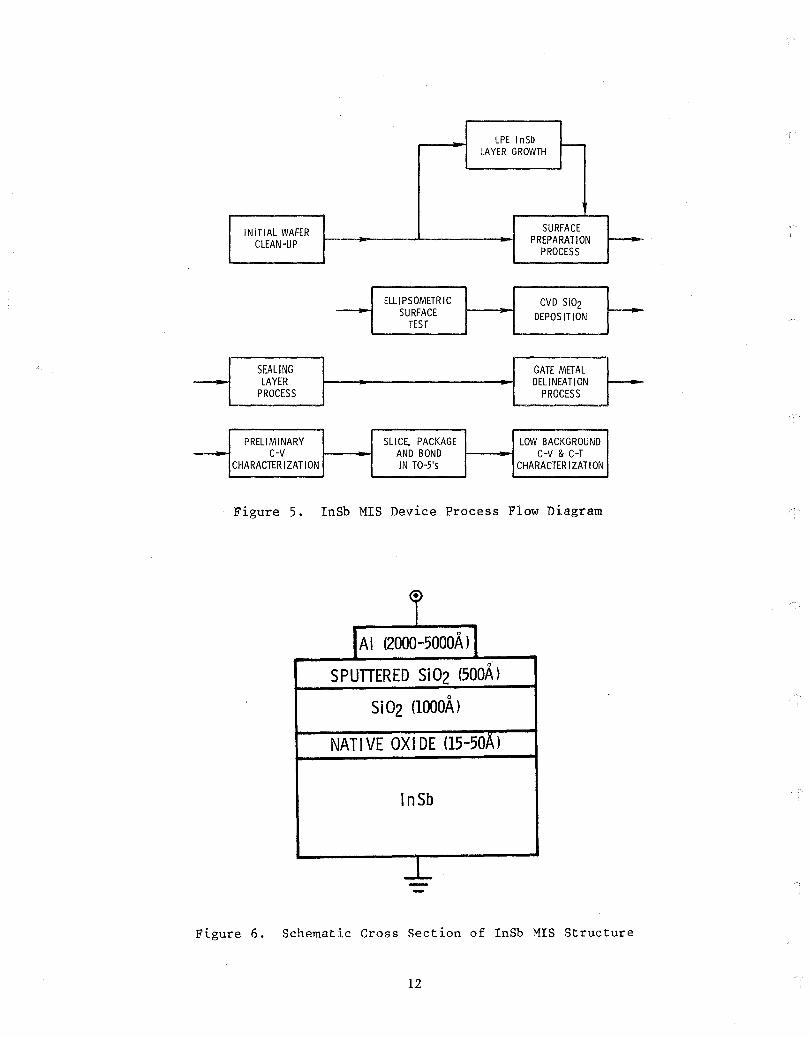
Section 2 MIS DEVICE FABRICATION AND CHARACTERIZATION
OF PECVD 8i02 ON InSb
The basic approach for surface passivation and fabrication of MIS devices
on lnSb, as described in Section 1, is based on theoretical arguments and has
grown out of IR&D research dating back to 1977. A flow diagram showing the
basic InSb MIS process sequence is shown in Figure 5. A schematic of the re
lated MIS structure is shown in Figure 6.
The basic MIS process is complex in that several of the operations require
critical etching steps which are subject to contamination problems. These can
be limited with good control of the etchants and industrial rinse water used.
A pre-deposition ellipsometric test is used as a control point to ensure that
the InSb wafer surface is clean prior to passivation. The process and device
characterization have been analyzed and reported by LanganlZand Thom, et al. 13
The previously used, pyrolytic CVD Si02 (HCVD and VCVD) deposition proc
esses required several parameters to be empirically evaluated and controlled to
ensure reasonable repetition in physical and electrical oxide quality. These
variables included: temperature, silane (8iH4) and oxygen (OZ) gas flow rates,
and time of deposition. Investigations of the necessary operating parameters
for producing quality oxides with the PECVD SiOZ reactor revealed several new
parameters which required evaluation and control before an established process
could be realized.
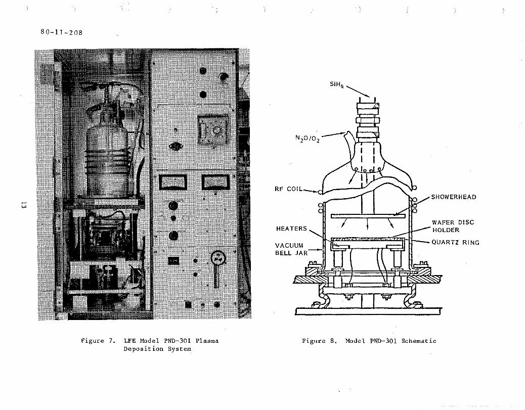
The PECVD system is an LFE Corporation Model PND-301. A photograph and
schematic view of the reactor are shown in Figures 7 and 8. Initial studies of
the deposited oxide quality were carried out at the Hughes Research Laboratory
in Malibu, California, but to pursue the approach further, a system was pur
chased from LFE Corporation in late 1979. The reactor consists of a 7.62-cm
(3-inch) diameter heated wafer holder contained in a small vacuum bell jar.
Silane (SiH4 ), diluted in argon, is admitted through a dispensing showerhead.
Nitrous oxide (NZO) is admitted at the top of the bell jar to serve as an oxi
dant. The reactant gases are excited by an inductively-coupled magnetic field
which surrounds the reacting chamber. The activated gases then react to form
8i02 which is deposited on the wafer surface.
A listing of the variable parameters requiring empirical evaluation, and
the ranges evaluated are shown in Table 1. In addition to the parameters shown
11
--
INITIAL WAFER CLEAN-UP
SEALING LAYER
PROCESS
PRELIMINARY C-V
CHARACTERIZATION
ELLIPSOMETRIC SURFACE
TEST
SLICE, PACKAGE AND BOND IN TO-5's
LPE I nSb I-LAYER GROWTH
SURFACE PREPARATION
PROCESS
CVD Si02 DEPOS ITION
GATE METAL DELINEATION
PROCESS
LOW BACKGROUND C-V & C-T
CHARACTER IZATION
Figure 5. InSb MIS Device Process Flow Diagram
r fAI (2000-5000A) I
0
SPUTTERED Si02 (500A) 0
Si02 (lOOOA)
NATI VE OXI DE (15-501\)
InSb
--L
I---
f-
Figure 6. Schematic Cross Section of InSb MIS Structure
12
....... Vl
80-11-208
Figure 7. LFE Model PND-30l Plasma Deposition System
SiH4~
RF COl L-__ A __ ....... SHOWERHEAD
VACUUM BELL JAR
lI---B uZI$<a;;m:;. .. ,:;;¢\i1ft,:;.:.~ QUARTZ RI NG
Figure 8. Model PND-301 Schematic

TABLE 1. PND-301 PECVD Si02 DEPOSITION PARAMETERS FOR InSb
Evaluation Range Item Variable Parameter
SI Units Actual Units
1 Substrate Temperature 20°-250°C ---2 RF Power 0-150 watts ---3 Pressure with SiH4 6.67-17.33 Pa 50-130 mTorr 4 Pressure with SiH4 + N20 12.00-33.99 Pa 90-255 mTorr 5 Showerhead Height 1.27-10.16 cm 0.50-4.00 inches
(Above Sample) 6 RF Coil Height 8.26-18.42 cm 3.25-7.25 inches
(Above Sample)
both N20 and 02 could be used as oxidizing gases (N20 preferred) and the se
quence in which the gases were admitted to the chamber could be interchanged
(although the system was set up to automatically inject SiH4 first). The final
parameter (one which proved to be major) was the type of showerhead used. An
aluminum showerhead was included as the standard unit with the system, but SBRC
[and Hughes Research Laboratories (HRL), Malibu] also purchased an optional
quartz dispensing head.
Initial investigations were performed with the standard metal showerhead
and involved varying the first four parameters of Table 1. Typical high-fre
quency (HF) and quasi-static (QS) low-frequency C-V, and conductance-voltage
(G-V) characteristics from these tests are shown in Figure 9. A major improve
ment in these characteristics was seen upon sWitching to the quartz showerhead 40r---~--'---.----r---r---.--~---.----.---.---'
30
I;i;: E- 20 u
10
SAMPLE 11-1 S-2370-2-5 200a e, 60 watts MEfAL SHOWERHEAD 500A SPUTIEREO Si02 OVERLAYER 8-HR ANNEAL
DATA 10 3311-2 f(HF) = 1 MHz T = 17K RAMP = 100 mv I sec I
I I
/
I I I I
".. I
G, 20 ~mho/div
~~6----+5--~~~~--~--~--+---+---~--~---4~~5
Figure 9. High-Frequency and Quasi-Static C-V Curves for PECVD Si02 lnSb MIS Sample Using Metal Showerhead
14

The initial test of the quartz showerhead used the best of the parameters de
termined from tests performed with the metal showerhead without attempting to
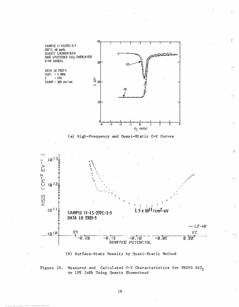
optimize them further. Figures 10(a) and (b) show the HF and QS C-V and sur
face state density (NSS) curves obtained from the initial trial on InSb. In
addition, storage time (Tc) measurements of these MIS devices (which were fab-v
ricated on LPE InSb layers grown on bulk InSb wafers) yielded values ranging up
to 22 seconds. The storage time was found to be basically bulk dominated by
Zerbst 14 analysis. Beyond the electrical characteristics, scanning electron
microscopy (SEM) examination of the PECVD Si02 surface indicated the oxide was
generally nongranular in nature as shown in Figure 11.
These results were quite significant and indicated that a gate insulator
which would ultimately yield the desired CTE values in CCIRIDs could be
achieved. The one remaining point of major"concern was related to the uniform
ity of the oxide deposited with the quartz showerhead. As shown in Figure 12,
a three-to-one thickness variation occurred across the wafer surface. Varia-
tion to this degree is unacceptable for CCIRID processing. Therefore, further
investigations were required to determine the operating parameters which would
yield both good electrical characteristics and uniform thickness. The major
task of the present contract was established with the intention of pursuing
several investigations in which different variables would be addressed in an
attempt to improve on the original results. Initially, tests were performed in
an attempt to repeat the original good results. These efforts were totally
unsuccessful indicating that one or more system variable(s), key to the suc
cessful deposition, was/were not precisely known.
A major problem confronted was a tendency for the system to generate vacuum
leaks. In conjunction with suggestions from personnel at HRL Malibu, and our
own findings, several changes were made to the system gas lines to improve the
vacuum integrity and flow rate control. An initial experiment (80-IX-13) was
set up .to reestablish the proper flow rates and pressure in the chamber of the
plasma deposition system after calibrating the capacitance manometer and per
forming the necessary repairs. It is reasonable to assume that, after several
repairs and a long period of time, operational conditions could have changed.
Also, these pressure experiments were performed earlier with the aluminum
showerhead but were never done with the quartz showerhead because of the early
good result. The experiment is summarized in Table 2.
15
" I
> W
N I 2: v '--'
Ul In Z
SAMPLE 1I-IS237C-I-5 200°C; 60 watts QUARTZ SHOWERHEAD 50DA S PUTTER ED S i 02 OVER LA YER 8-HR ANNEAL
DATA I D 3303-5 f(HF) = 1 MHz T = 17K RAMP = 100 mv I sec
30
10
~~4--~--~--~--~---+---+2---+3--~4
10 13
10 Ie
10 I r
VG (volts)
(a) High-Frequency and Quasi-Static C-V Curves
. \ # ,
.\ ...• ~ 0. ~ .
'.
SAMPLE 1'-IS-237C-I-5 DATA I D 3303-5
. . . . . . 1.5 x lOll, cm2-eV
,. ... -.....
--IF-HF
EV EC + -~.f.'2]--'-'-·' =0 -.~-'---'---- --:~i:~ 0--------=0~~--------·H~~-' '-'-'-.... _.10. 1 £]
SURFACE POTENTIAL
(b) Surface-State Density by Quasi-Static Method
Figure 10. Measured and Calculated C-V Characteristics for PECVD Si02 on LPE lnSb Using Quartz Showerhead
16

Showerhead: Quartz
Temperature: 200°C
RF Power: 60 watts
Total Pressure: 26.66 Pa
O/S (Pressure): (200 mTorr
0.82
Showerhead Height: 2.2 cm
RF Coil Height: 10.8 cm
1000A PECVD Si02 + SOOA
RF Sputtered SiOZ
80-12-11
Visible Grains: 1000A Diameter
Base Layer: Nongranular
Figure 11. PECVD Si02 Granularity for InSb Sample: II-IS 237C
1800 A
1500
4.5 cm
Figure 12. Illustration Showing Oxide Thickness Variation over a Wafer Surface Resulting from the Deposition Parameters Used for the Device in Figures 10 and 11
17
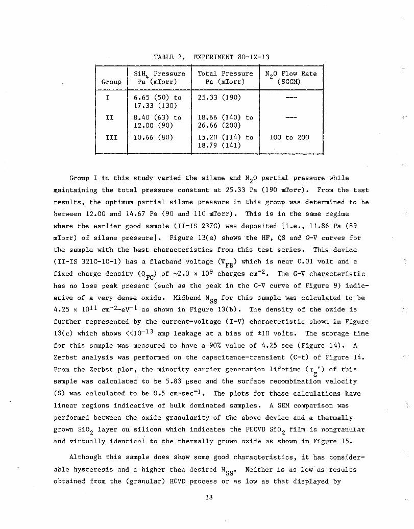
TABLE 2. EXPERIMENT 80-1X-13
SiH4 Pressure Total Pressure N20 Flow Rate Group Pa (mTorr) Pa (mTorr) (SCCM)
I 6.65 (50) to 25.33 (190) ---17.33 (130)
II 8.40 (63) to 18.66 (140) to ---12.00 (90) 26.66 (200)
III 10.66 (80) 15.20 (114) to 100 to 200 18.79 (141)
Group I in this study varied the silane and N20 partial pressure while
maintaining the total pressure constant at 25.33 Pa (190 mTorr). From the test
results, the optimum partial silane pressure in this group was determined to be
between 12.00 and 14.67 Pa (90 and 110 mTorr). This is in the same regime
where the earlier good sample (II-IS 237C) was deposited [i.e., 11.86 Pa (89
mTorr) of silane pressure]. Figure 13(a) shows the HF, QS and G-V curves for
the sample with the best characteristics from this test series. This device
(II-IS 321C-10-1) has a flatband voltage (VFB ) which is near 0.01 volt and a
fixed charge density (QFC) of ~2.0 x 10 9 charges cm-2 • The G-V characteristic
has no loss peak present (such as the peak in the G-V curve of Figure 9) indic
ative of a very dense oxide. Midband NSS for this sample was calculated to be
4.25 x lOll cm-2-eV-l as shown in Figure 13(b). The density of the oxide is
further represented by the current-voltage (I-V) characteristic shown in Figure
13(c) which shows «10-13 amp leakage at a bias of ±10 volts. The storage time
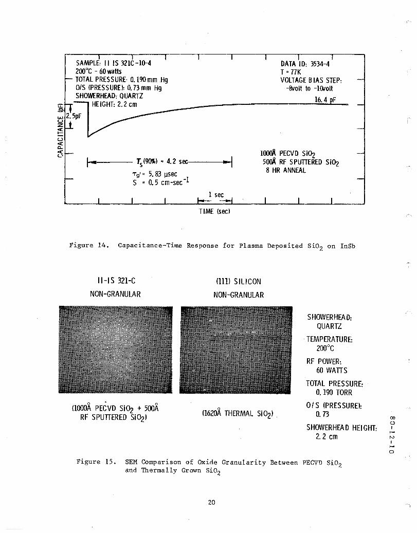
for this sample was measured to have a 90% value of 4.25 sec (Figure 14). A
Zerbst analysis was performed on the capacitance-transient (C-t) of Figure 14.
From the Zerbst plot, the minority carrier generation lifetime (T ') of this g
sample was calculated to be 5.83 ~sec and the surface recombination velocity
(S) was calculated to be 0.5 em-see-I. The plots for these calculations have
linear regions indicative of bulk dominated samples. A SEM comparison was
performed between the oxide granularity of the above device and a thermally
grown Si02 layer on silicon which indicates the PECVD Si02 film is nongranular
and virtually identical to the thermally grown oxide as shown in Figure 15.
Although this sample does show some good characteristics, it has consider
able hysteresis and a higher than desired NSS ' Neither is as low as results
obtained from the (granular) HCVD process or as low as that displayed by
18
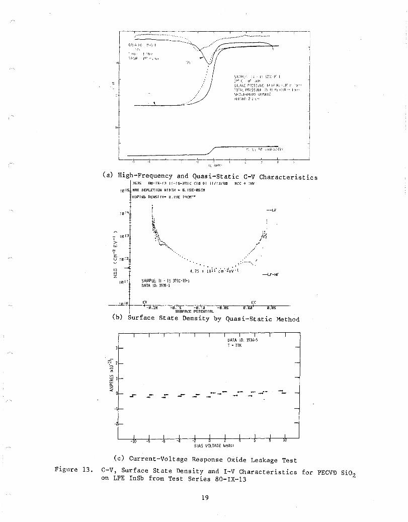
Figure 13.
t-i
I ..................... " .' ----.... _ ... D'\IA I D 3S3\! T 771-
I '.IHz Ill!) "1\5<'(
J\
:
......... ..... ....................
--====:::::::"I-
S,V.IPLE II· IS 31ll··I"I ?f''1 C . h0 :.dttS
[ , S II ~"'E PRES SUkE Id 07 Pa ,1lC ,., l1rr' TOTM PRESSURE· 2),33 0d Ilqn :" TiP" SHOI'.ERHEAD OU,~RTZ
HEIGHL 1.1 (1'1
I '"
------_/ L---.1-; --.+.,---'-----7---:'t.---'~--'----+---L--+--'----'
(a) High-Frequency and Quasi-Static C-V Characteristics
I
> W
N I L: V
ill ill Z
3S3S 8Z-IX-13 1I-IS-32IC CIZ DI 11/13/8Z RCC ~ INV
IZ I HAX DEPLETION WIDTH e 6. ISE-m5CH
DOP I N6 DENS I TYe 8. 19E I'1CH-'
........
:: ........ . 4.25 x ;oil' c'm'-ie~: 1
SAMPLE: II - IS 32le-IO-1 DATA 10: 3535-1
-L,
:. --J /~':
I"
1m EV EC -Z.2Z -0. IS -Z.la -z.as a.HZ a.zs
SURfRCE POTENT I AL
(b) Surface State Density by Quasi-Static Method
-1
-2
.~ - -- ---
DATA 10, 3534-5 T " 17K
----
B lAS VOLTAGE (volts)
--
(c) Current-Voltage Response Oxide Leakage Test
C-V, Surface State Density and I-V Characteristics for PECVD SiOz on LPE InSb from Test Series 80-1X-13
19
SAMPLE: II IS 321C-I0-4 200°C - 60 watts TOTAL PRESSURE: O.I90mm Hg OIS (PRES SURE h 0.73 mm Hg SHO~RHEAO:QUARTZ
DATA 10: 3534-4 T = 17K VOLTAGE B lAS STEP:
-Bvolt to -HNoit
~~ L.&J 2.SpF u :z ~
16.4 pF
u « a.. « c...'
... 1 ............ --- Ts(~) = 4.2 sec:------... ~I
Tg' = 5. 83 ~sec S = 0.5 cm-sec-1
lOOGl\ PECVO Si02 500ll RF SPUTIEREO Si02 8 HR ANNEAL
TIME (sec)
Figure 14. Capacitance-Time Response for Plasma Deposited Si02 on InSb
II-I S 321-C
NON-GRANULAR
o 0
(lOOOA PECVD Si02 + 500A RF SPUTTERED Si02)
(Ill) SILICON
NON-GRANULAR
o (l620A THERMAL Si02)
SHOWER HEA 0: QUARTZ
TEMPERATURE: 200°C
RF POWER: 60 WAITS
TOTAL PRESSURE: 0.190 TORR
01 S (PRES SURE): O. 73
SHOWERHEA D HEI GHT: 2.2 em
Figure 15. SEM Comparison of Oxide Granularity Between PECVD Si02 and Thermally Grown Si02
20
00 o , ..... N J .....
o
II-IS 237C. Significantly, the oxides so produced do lack the granularity that
plagued the HCVD films used in the earlier CCDs, which was the motivation for
pursuing the PECVD process.
The other samples in Group I had C-V characteristics that were degraded as
the silane pressure was either increased or decreased from the optimum of 14.67
Pa (110 mTorr). In addition, the oxide uniformity became even more nonuniform
than in Figure 12 and also became granular with a mean diameter of ~.125 ~m.
The Group II samples were coated by holding the silane/oxidant (SiH4/N20)
ratio constant at 0.45 while the total pressure was varied. In Group III sam
ple depositions, the silane pressure was held constant, while the N20 pressure
was varied. For this group, the N20 flow rate was measured with a newly in
stalled mass flow meter in the N20 line. All other variables -- showerhead
height, RF power, RF coil height, and temperature -- were held constant and at
those settings associated with the earlier good results. Within the ranges
investigated for these two groups, no observable relationships between C-V
quality and pressure or flow settings were realized.
RF COIL HEIGHT EXPERIt1ENT (80-IX-14)
The purpose of this experiment was to determine the optimum RF coil height
for the PND-301 system. The coil height is not fixed and can be easily moved
up and down the bell jar. It was hypothesized that during earlier tests, the
coil position had not been accurately controlled and movement may have had a
degrading effect on the results, or that the optimum position had not yet been
established.
Four depositions were performed with coil heights of 8.26 cm (3.25 inches)
(as measured from the bottom of the lowest turn to the baseplate), 10.80 cm
(4.25 inches), 13.34 cm (5.25 inches), and 18.42 cm (7.25 inches). All other
parameters were held constant at the settings listed in Table 3.
21
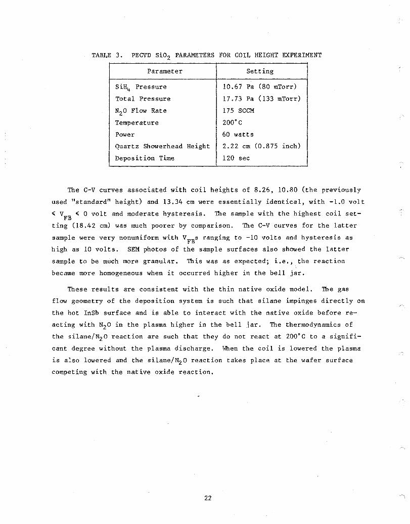
TABLE 3. PECVD Si02 PARAMETERS FOR COIL HEIGHT EXPERIMENT
Parameter Setting
SiH4 Pressure 10.67 Pa (80 mTorr)
Total Pressure 17.73 Pa (133 mTorr)
N20 Flow Rate 175 SCCM
Temperature 200°C
Power 60 watts
Quartz Showerhead Height 2.22 cm (0.875 inch)
Deposition Time 120 sec
The c-v curves associated with coil heights of 8.26, 10.80 (the previously
used "standard" height) and 13.34 cm were essentially identical, with -1.0 volt
~ VFB
~ a volt and moderate hysteresis. The sample with the highest coil set
ting (18.42 cm) was much poorer by comparison. The C-V curves for the latter
sample were very nonuniform with VFBs ranging to -10 volts and hysteresis as
high as 10 volts. SEM photos of the sample surfaces also showed the latter
sample to be much more granular. This was as expected; i.e., the reaction
became more homogeneous when it occurred higher in the bell jar.
These results are consistent with the thin native oxide model. The gas
flow geometry of the deposition system is such that silane impinges directly on
the hot InSb surface and is able to interact with the native oxide before re
acting with N2 0 in the plasma higher in the bell jar. The thermodynamics of
the silane/N2 0 reaction are such that they do not react at 200°C to a signifi
cant degree without the plasma discharge. When the coil is lowered the plasma
is also lowered and the silane/N2 0 reaction takes place at the wafer surface
competing with the native oxide reaction.
22
ELLIPSOMETRY EVALUATION
A Gaertner L117 ellipsometer was used routinely as an in-process check to
determine the extent of cleanliness of freshly etched InSb surfaces, study the
effect of the plasma deposition on the native oxide, and determine Si0 2 film
quality by calculating the index of refraction of a sample film deposited on
silicon.
The use of the ellipsometer to evaluate the degree of InSb surface cleanli-
ness has been previously reported by Langan. IS
surfaces were measured to determine the complex
A Ok n3 = n - 1
In his work, cleaved <110) InSb
index of refraction
(1)
for the thin native oxide. From these studies an effective InSb substrate
index of A3 = 4.36 - 1.65i was determined to be the cleanest surface obtainable
without working in a vacuum.
ble ellipsometer readings of
phase change (~) = 148.60.
This complex number was associated with measura
relative amplitude change (~) = 18.65 and relative
The values ~ and ~ are used to track the index of refraction and oxide
thickness. The measured ~ and ~ values are iterated through a program, de
scribed by Loser and Lars~n,17 which was modified for use on a Hewlett-Packard
MXI000 computer.
Results of the cleaved InSb study indicated that a native oxide ~15A
thick is immediately grown upon exposing the InSb surface to atmospheric condi
tions. Similar test results indicated the cleanest InSb surface obtainable
following an etch process had a native oxide ~45A thick and an index of refrac
tion near 3.6. These correlate with ~ and ~ values of 19.5 and 140.8, respec
tively.
Significant variation from these values is indicative of a nontypical sur
face, usually due to contamination, and can be correlated with poor C-V re
sults. Therefore, wafers are checked with the ellipsometer after the surface
cleanup etch to determine if the wafer requires additional cleaning before
proceeding with the deposition.
Ellipsometric Native Oxide Analysis
To determine the effect of a plasma discharge on the native oxide, an ex
periment was performed in which cleaned wafer surfaces were exposed to various
phases of the plasma deposition sequence. Ellipsometric measurements were
taken before and after exposure, in an attempt to detect variation in the
native oxide condition.
23

The observed effect on an InSb wafer from a l20-second "soak" at a tempera
ture of 200°C (under normal vacuum, no gases admitted, and the plasma left off)
was a subtle change in the native oxide thickness and/or composition as indi
cated by the following ellipsometer readings:
1. $ and ~ before heat exposure: 19.30; 141.50
2. $ and ~ after heat exposure: 19.50; 140.00
This was hypothesized to be related to residual oxygen remaining in the vacuum
chamber.
The effect of exposure to the plasma at 200°C (still with no gases admitted
to the chamber) was predictable in that in each case substantial thickening of
the native oxide was observed as shown in Table 4.
TABLE 4. EFFECTS OF PLASMA EXPOSURE ON InSb THIN NATIVE OXIDE
Approximate Power (watts) Time (sec) Native Oxide
Thickness (A)
20 120 70 60 120 70
100 120 85
In each case, the index of refraction decreased from 3.0 to 2.3 with no
marked change in k (dispersion coefficient). It is difficult to state exactly
what caused this decrease since segregation of indium and antimony can occur
without the ellipsometer detecting it.
Of serious concern was the automatic deposition sequence of the reactor in
which diluted silane is admitted and flows for 180 seconds prior to the plasma
being ignited. Since silane is injected from the showerhead directly onto the
wafer surface, it is conceivable the native oxide could be reduced, thereby
degrading the interface characteristics. It should be noted, however, that the
previously-produced excellent sample (II-IS-237C) utilized tQ,is very same se
quence. Ellipsometric readings of the surface, after exposure to silane at
200°C for varying times, failed to show any change in its condition; i.e., $
and ~ remained unchanged.
24

To further analyze this condition, an ESCA analysis was performed at the
Jet Propulsion Laboratory in Pasadena, California. This analysis indicated
that, after exposure to silane for 5 minutes, the native oxide (originally
In203) was in a reduced form and an oxidized form of silicon was present on the
wafer surface.
In concluding this investigation, the ellipsometer was found to be capable
of detecting small changes in the thickness and refractive index of the thin
native oxide. Small changes in chemical composition, however, which might
markedly affect electrical characteristics, will not necessarily change the
optical properties sufficiently to be detectable.
Ellipsometric Analysis of CVD SiO?
The ellipsometer can effectively monitor the quality of deposited Si02 and
was used to evaluate CVD Si02 films as deposited on silicon. One method of
characterizing a thin film is to take single-point measurements using various
angles of the incident beam. For a good quality oxide, the $ and 8 values for
each angle should yield the same index of refraction and thickness when the
data are reduced by the computer program.
Three samples representing VCVD, HCVD, and PECVD Si02 films were selected
for this test. The $ and 8 values were recorded for each sample at three dif
ferent incident angles (30°, 50°, and 70°). The index of refraction was ob
tained assuming nonabsorbing or nearly nonabsorbing films and minimizing the
error.
Figure 16 shows the results of the measurements for these samples. As
shown, the HCVD and VCVD oxides are typically well behaved and uniform; i.e.,
the calculated index does not vary greatly with ellipsometer angle. PECVD Si02 is similarly well behaved in certain regions of some samples, as shown by the
curve labeled "good region." However, it is nonuniform over the entire wafer,
and in other regions the index varies greatly with ellipsometer angle, indicat
ing the Si02 has nonideal characteristics in these regions. The nonlinearity
in the "nonuniform" region can perhaps be attributed to improperly assuming the
film is nonabsorbing which would result in erroneous index of refraction
values.
25
Vl UJ UJ ~ <..!) UJ 0
§ UJ u z UJ 0 -u z w... o
70
50
UJ 30 ....J <..!) Z <:
1. 35 1.40 1.45 INDEX OF REFRACTION (nf)
G= nf VERSUS rJ FOR TYPICAL HCVD OXt DE
&= nf VERSUS" FOR TYPICAL VCVD OXI DE
1. 50
0" nf VERSUS 0 FOR PECVD OXIDE (NON-UNIFORM REGION)
0- nf VERSUS 0 FOR PECVD OXIDE (GOOD REGION)
Figure 16. Measured Index of Refraction versus Ellipsometer Angle for Various CVD Si02 Samples
DEPOSITION UNIFORMITY
It has been observed on large silicon wafers used as trial substrates that
the refractive index varies significantly about the center of the PND-301 wafer
platen. In a single deposition the index may vary from 1.36 to 1.46 as shown
in Figure 17. As the refractive index is an indication of the quality of the
oxide, it ~s important that the wafer be always placed in the best position
with respect to the platen, showerhead, RF coil, etc. The quartz showerhead
(Figure 18), which provides better C-V characteristics than the metal shower
head, consists of a quartz ring with several holes for gas dispersion. Since
the holes were pulled by hand, the spacing and orientation are not uniform.
Thus, the silane gas flow is critically dependent on the placemen.~ of the
showerhead.
Because standard InSb test samples (quarter-wafers) are small (~1.3 cm x
1.3 em), it is difficult to determine whether variations in MIS C-V data occur
as a result of edge effects or real variations in the deposition system.
Therefore, an experiment was performed to correlate C-V data with areas of good
and poor refractive index. A full size InSb wafer (3.2-cm diameter) was placed
on the platen as shown in Figure 19. The C-V data accumulated are summarized
26

WAFER PLATEN
/- ......
/ '" 7.62 em (3 in.) DIAMETER
I \ __ - _I, 1. 45 I ,. ,
, \ I " 1.46 \ I
.... t- ~ ...... r---,../ " \ '- 1. 36 \,
.........
\.. 1. 43' /
"-"~""'J
Figure 17. Variation in Index of Refraction of a Typical PECVD Si02 Film (Dotted lines show tendencies and are not exact)
Figure 18. PND-301 PECVD System Quartz Showerhead
27
WAFER PLATEN 7.62 cm (3 inches) DIAMETER
FRONT OF REACTOR
t
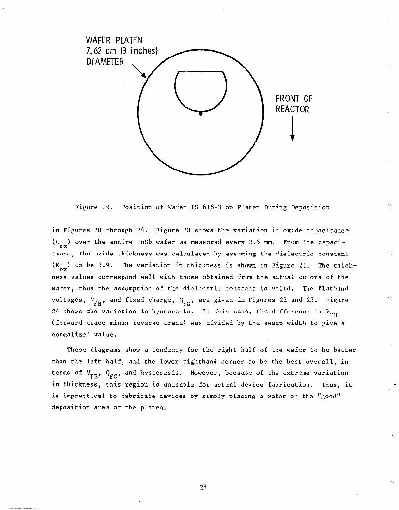
Figure 19. position of Wafer IS 618-3 on Platen During Deposition
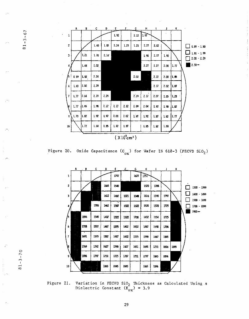
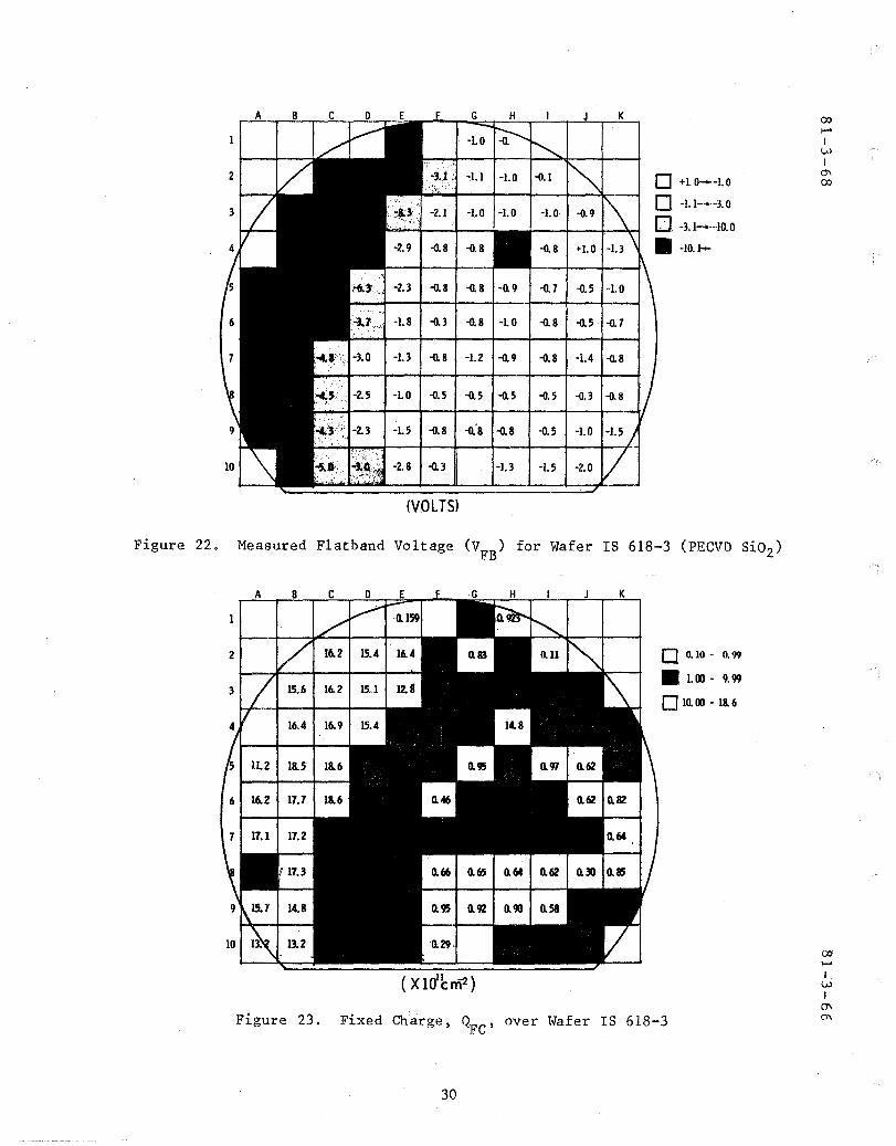
~n Figures 20 through 24. Figure 20 shows the variation ~n oxide capacitance
(C ) over the entire InSb wafer as measured every 2.5 mm. From the c~paciox
tance, the oxide thickness was calculated by assuming the dielectric constant
(K ) to be 3.9. The variation in thickness is shown in Figure 21. The thick-ox
ness values correspond well with those obtained from the actual colors of the
wafer, thus the assumption of the dielectric constant is valid. The flatband
voltages, VFB , and fixed charge, QFC' are given in Figures 22 and 23. Figure
24 shows the variation in hysteresis. In this case, the difference in VFB
(forward trace minus reverse trace) was divided by the sweep width to give a
normalized value.
These diagrams show a tendency for the right half of the wafer to be better
than the left half, and the lower righthand corner to be the best overall, in
terms of VFB , QFC' and hysteresis. However, because of the extreme variation
in thickness, this region is unusable for actual device fabrication. Thus, it
~s impractical to fabricate devices by simply placing a wafer on the "good"
deposition area of the platen.
28
00.89 -1.80
2.17 01.81-1.99
o 2.00 - 2.29
1.48 2.27 2.00 .2.30-
1.82 2.00
2.02 .2.02 1.87
04 2.19 2.17 2.07 1.85 1.28
1.95 1.98 2.12 2.17 2.12 2.09 2.04 1.97 1.90 1.82
1.82 1.92 1.97 2.00 2.02 1. 97 1.92 1.87 1.82
1.80 1.85 1.87 1.87 1.85 1.82
( X lO8cm2 )
Figure 20. Oxide Capacitance (C ) ox
for Wafer IS 618-3 (PECVD Si02)
2 0 1300 - 1399
1321 1348 1816 1590 0 1400 - 1499
0 1500 - 1699
1307 1322 1322 1520 1520 o 1700 - 1899 .1900-1540 1402 1322 1322 1'108 1432 1554
1507 1487 1315 1402 1432 1487 1590
1575 1507. 1487 1432 1575 1590 1667
1742 1627 1590 1627 1651 1691 1751 0 ......
1751 1725 I 1107 1751 1797 1845 (¥)
I ,..., 1845 1845 . 1865 00
Figure 21. Variation in PECVD Si02 Thickness as Calculated Using a Dielectric Constant (Kox) = 3.9
29
2 o +1.0--1.0
o -1.1--3.0
o -3.1--10.0
+1.0 • -10.1-
-2.3 -0.& -0.8 -0.9 -{J.7 -{J.5
-0.3 -0.8 -1.0 -0.8 -0.5 . -{J.T
-0.8 -1.2 -0.9 -{J.8 -1.4 -0.&
-1.0 -0.5 -0.5 -0.5 -{J.5 -{J.3 -{J.8
-{J.8 -0:8 -0.8 -{J.5 -1.0
-0.3 -1.3 -1. 5
(VOLTS)
Figure 22. Measured Flatband Voltage (VFB
) for Wafer IS 618-3 (PECVD Si02)
2 0 0.10 - 0.99
• 1.00 - 9.99
010.00 - 18.6
Figure 23. Fixed Charge, QFC' over Wafer IS 618-3
30
00 I-'
I W I 0\ 00
00 I-"
I W I 0\ 0"1

0"< '-0
I C'I")
I ..... co
2 o 0.07 - 0.10
CJ 0.11 - 0.12
• 0.13 - 0.14
o 0.15 - 0.11
Figure 24. Normalized C-V Hysteresis (~VFB/~VG)' Wafer IS 618-3
ESCA STUDY OF PECVD Si02 ON InSb
An experiment using ESCA, with an ion etching technique, to profile a PECVD
Si02 sample on InSb was performed at Surface Science Laboratories in Palo Alto,
California. With this technique, chemical information was obtained as a func
tion of etch time. In a 1978 IR&D study, similar analyses were performed on
InSb samples with horizontal and vertical CVD Si02 layers. The objective of
this experiment was to gather data on the effect of plasma deposit~on on the
Si02 /InSb interface and to compare these results with interface results from
the pyrolytic oxides studied earlier.
One of the difficulties encountered 1n understanding the nature of the
interface resulting from plasma deposited Si02 stems from the inability to make
direct electrical correlations. As has been established, any given deposition
is nonuniform across the 7.62-cm wafer platen. Therefore, it is unreliable to
deposit on two samples simultaneously (one for an MIS structure and the other
for ESCA) and assume they are identical. Similarly, the deposition is not
reproducible; a subsequent deposition is not necessarily the same as the first.
It is also not possible to analyze testable MIS structures by ESCA, because
31
of thickness nonuniformities resulting from removing the metal gate. Also,
the interface becomes diffuse when a thick (500A to lOOOA) sample is analyzed.
Thus, one has no assurance that a single PECVD analysis is in any way represen
tative of a typical PECVD sample.
In spite of these difficulties, some differences and similarities between
PECVD and pyrolytic CVD samples are noted.
Differences
1. Contrary to pyrolytic CVD samples, the PECVD sample did not show an Sbrich region at the native oxide/substrate interface. Figures 25, 26, and 27 show In/Sb atom ratios as a function of etch time for all three reactors. Examining the 3d lines (which are "shallower" electrons), it can be seen in Figures 25 and 26 that the ratio drops before reaching a bulk value of about 1.3 for the pyrolytic CVD samples. The relative amount of Sb at this point is higher than in the·bulk. (The bulk value of 1.3 is an artifact of the instrument and does not imply a nonstoichiometric substrate.) The PECVD sample (Figure 27) shows a slow decrease to the bulk value of 1.2 for 3d electrons.
2. There is no evidence for the presence of antimony oxides anywhere in the PECVD or vertical CVD samples as analyzed by Surface Science Laboratories. It is possible that antimony oxides were reduced by the ion beam during the analysis process. Another analysis performed on horizontally-deposited CVD samples indicated that traces of antimony oxide possibly existed at the interface. ESCA studies of VCVD and HCVD samples performed by JPL using a chemical depth profile etch technique, showed a possibility that substantial amounts of antimony oxides were present. Samples of PECVD Si02 on InSb were also sent to JPL for analysis but, due to scheduling and system difficulties, were not concluded.
3. Indium is present in the PECVD sample primarily in the elemental form with a small amount of oxide also detected at certain etch points. The maximum amount of oxide present is small, on the order of a few percent similar to that observed for the vertically-deposited Si0 2 and much less than observed for the horizontally-deposited sample. In each case the oxide/elemental ratio was greatest away from the interface and decreased as the interface was approached.
Similarities
1. In all three samples an In-rich region was found Ln the Si02 layer at the beginning of the interfacial region.
2. The O/Si ratios as a function of etch time are seen to decrease from a value near 2 observed in the Si02 to a value near 1.5 at the interface. Accompanying this deficiency is the appearance of a weak shoulder on the low binding energy side of the main Si(2p) line which may indicate the presence of a reduced form of Si.
32

6
5 FIRST DETECTIO
OF In 0 AND Sb l-e( 4 0::
:?: w 0 w l-e(
~ 3 c -
2
1
10
Figure 25.
o 3d (5/2) ~4d
BULK
I
lIO
In/Sb Ratio as a Function of Etch Time for Vertical CVD Si02 Deposited on lnSb
0 i= < ~
~ I-< .&:l VI
c::
6.98 '
5.0,.,...--..,--+--.,----.,---.,......--....,...--""""1"-----,
4.5
4.0
3.5
3.0
2.5
4d: • 2.0
3d: 0
FIRST DETECTION OF In AND Sb
BULK InSb
0.5
o o 5 10 15 20 25 30 ETCH TIME (min)
Figure 26. In/Sb Ratio as a Function of Etch Time for Horizontal CVD Si02 Deposited on InSb
34
35
6. 6O.-----3--...,...---r----,---~r__-__,.--~--....,
6.00
5.
4.
4. o =c a:: :E ~ 3 . ..::I VI
~1 -3.
2.
1.
1
FIRST DETECTION OF In AND Sb
3d: 0
4d: •
O·00b----~7~O-----OO*---~=---~~--~~----~1~~--~lO
Figure 27. In/Sb Ratio as a Function of Etch Time for PECVD SiOz Deposited on InSb
35

FINAL EVALUATIONS OF PECVD Si02 ON InSb
From the test results that have been discussed, it is clear that the non
uniformity and repeatability of the oxide, resulting from using the quartz
showerhead, must be improved before PECVD Si02 is useful for InSb imager fabri
cation.Total pressure, gas ratios, showerhead height and RF coil height have
been extensively varied without substantial improvements in either uniformity
or repeatability of the Si02 layers deposited with the quartz showerhead.
There are three possible solutions to this problem:
1. modify the quartz showerhead design to disperse the silane more uniformly over the platen and reduce turbulent flow;
2. modify the system, if possible, to premix the silane with the nitrous oxide prior to or simultaneous with admission to the reaction chamber; or
3. modify the system, if possible, to rotate either the quartz showerhead (or a newly-designed dispersion head) or the platen.
Material and hardware to investigate potential solutions (1) and (2) were
ordered. Quartz plates and diamond drills were received and fabrication of a
new quartz showerhead (option 1), similar to the aluminum plate showerhead, was
initiated. But, the contract technical period expired before assembly could be
completed. Option (3) was considered to be too costly and would require a
considerable outlay in capital before it could be performed. The hardware for
option (2) was ordered and assembled in the reactor, and experiments were ini
tiated prior to the end of the contract period.
A final experiment was performed following reworking the PND-30l gas lines
to allow the reactant gases (SiH4 and N20) to be premixed prior to being admit
ted into the bell jar. The mixed gases were then distributed through the
showerhead. For this test, both the existing quartz and metal showerheads were
used. The fundamental purpose of the experiment was to determine the effect on
uniformity. In addition, one of the tests included mounting the wafer on the
platen at room temperature and allowing the substrate to heat to 200°C in vac
uum. (This had not been done previously because the temperature controller
overshoots ~50°C unless it is very slowly increased to the set point.) For the
test, the temperature was increased from 20°C to 200°C over a period of 2.52 x
103 seconds (42 minutes). Even at this rate, the temperature overshot to
~245°C.
36
Initially when using the quartz showerhead, the deposition nonuniformity
increased with the premixed configuration. The total pressure was then reduced
by one-half, keeping the gas ratios approximately the same. This resulted in
an extremely uniform coating which varied only 15% over a circular area ~5 cm
in diameter. The index of refraction of this Si02 was uniformly 1.46 and ini
tially reproducible from run to run.
The HF and QS C-V and G-V curves showing the characteristics achieved with
the quartz showerhead (heated from 25°C to 200°C under vacuum) are shown in
Figure 28.
~fue data are encouraging in that they show a flatband voltage which is near
zero and hysteresis of ~0.1 volt. Discouragingly, there is a high loss peak in
the G-V curve near zero volts. Current-voltage tests of these devices yielded
a 77K leakage current on the order of 5 x 10-11 amp at a bias of ±3.0 volts.
The NSS for the device is shown in Figure 29 and has a minimum value of 3.6
x lOll cm-l-eV-l, although the minimum is shifted from midband to within 0.083eV
8HX-05 SAMPLE: I S618-lOC -D3 DEPOS mON TEMP: 200°C STARTING TEMP: 25°C QUARTZ SHOWER HEAD PREMIXED GASES
u.. CI.
lLI U Z ;:: u « a.. « u
40
30
20
10
-5 -4
..........
HF
G -V 2O!.tmho/div
-3 -2 -1 0 1 2 3 4 GATE BIAS-VOLTS
Figure 28. C-V Characteristics, PECVD Si02 on InSb
37
6484 SI-IX-OS Is6IS-IOC CI D3 4/29/81
1014 MAX ~EPlETION WI~TH = 2.34E-04CM
DDPIN6 ~ENSITYc 4.33E 13CM-3
ACC ~ INV
MINIMUM NSS
• 3.6 x lOll cm-2 -eV-l
""1£1 13 • :. I \r-J ... > w
.'-... .. II! I .-.. I: -··"-·.0. V v
LIlol2 ... Ln DEPOS ITiON TEMP: 200°C z
STARTING TEMP: 25°C ... . . QUARTZ SHOWER HEAD PREMIXED GASES
-Lf-Hf
-If
J J EV EC --~~+------~a~~·~a~~~2=0----~0~~~J~s----~a~~~I~a~--~0;+~~0~s~~0~~~0~~~~0~~~8~S~--8~"~.~18~~8~IS
sURfRCE POTENTIAL
Figure 29. Surface State Density, PECVD Si02 on InSb
of the conductance band. SEM examinations were conducted on the various films
deposited. These showed a tendency toward some granularity which was not as
good as seen with the very good PECVD samples but much better than the HCVD
samples.
Tests using the metal showerhead were, in general, a bit worse than with
the quartz showerhead, although no optimization of either was performed.
CONCLUSIONS OF PECVD Si02 EVALUTION
Based on the results of the studies that have been carried out on IR&D as
well as this program, it has been determined the PECVD Si02 deposition parame
ters associated with the best InSb MIS C-V characteristics are as shown in
Table 5. These parameters are known to yield occasional samples with good to
excellent quality. The depositions associated with these parameters are still
nonuniform and nonrepeatable.
Some trends toward uniformity and repeatability improvement were seen with
premixing the gases and heating the substrate under vacuum, but these deposi
tion processes have not been optimized.
38
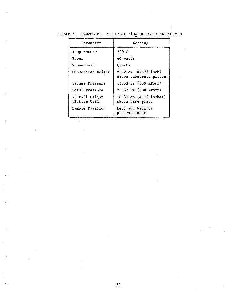
TABLE 5. PARAMETERS FOR PECVD Si02 DEPOSITIONS ON InSb
Parameter Setting
Temperature 200°C
Power 60 watts
Showerhead Quartz
Showerhead Height 2.22 em (0.875 inch) above substrate platen
Silane Pressure 13.33 Pa (loo mTorr)
Total Pressure 26.67 Pa (200 mTorr)
RF Coil Height 10.80 cm (4.25 inches) (Bottom Coil) above base plate
Sample Position Left and back of platen center
39

(THIS PAGE INTENTIONALLY LEFT BLANK)
40

Section 3
EVALUATION OF HCVD/HCl SiOZ ON InSb MIS DEVICES
Through the introduction of a small amount of HCI in the gas stream during
CVD SiOz deposition, some investigators have been able to significantly reduce
interface states and distributed charge within the oxide. 17 ,18 The HF C-V
results of a 1981 IR&D experiment performed at the Naval Oceans Systems Center,
San Diego, are shown in Figure 30. It is clear from these trials that the
presence of HCl considerably reduced the flatband voltage, hysteresis, and NSS '
.......... . . . . . . . . . . '
." .......... CONTROL SAMPLE IS 594-12C no HCL
. ' .............
-50 -45 -40 -35 -30 -25 -20 -15 -10 -5
V G (volts)
10
90
Figure 30. High-Frequency C-V Curves for NOSC Experiment Using HCl in a PECVD Deposition
In order to continue these experiments locally, the Applied Materials AHS-
2600 horizontal-flow CVD reactor was modified to handle HCI. Two preliminary
depositions were made using standard SiH4 , 0z and NzO flow rates of 32 SCCM, 60
sceM and 22 SLM, respectively. In the first deposition, 13 SCCM of HCI was
allowed to flow diluted in Nz for 300 seconds prior to deposition, and then
continued for 60 seconds after the SiH4 and 0z were admitted. This resulted in
a surface which appeared severely pitted, presumably etched by the HCI. For
the second deposition, the same sequence was followed; however, the HCl was
41

reduced to an unmeasurable trickle of gas. In this case the results were simi
lar. Dilute HCI (5% in nitrogen) was then ordered and new investigations per
formed.
In the second series of tests, the diluted HCI gas was admitted for periods
of 60 to 300 seconds prior to admitting SiH4 and OZ' The flow was regulated at
~50% of full scale for the same rotometer previously used (actual flow rate is
not known). Next, SiH4 and 0z were added for 60 seconds and then the HCI gas
shut off. The SiH4 and 0z were then allowed to flow for a period to achieve an
oxide ~1500A thick, after which capacitors were delineated.
The C-V analysis of these devices was nonconclusive as the devices fabri
cated with HCI were nearly identical to control devices fabricated without HCI.
The result has two possible reasons:
1. the flow rate of dilute HCI gas was insufficient to perform any device improvement, or
2. the oxide fabricated with the HCVD system is already better than the HCI gas can help to obtain.
Considerably more evaluation would be required to prove either of these
hypotheses.
42
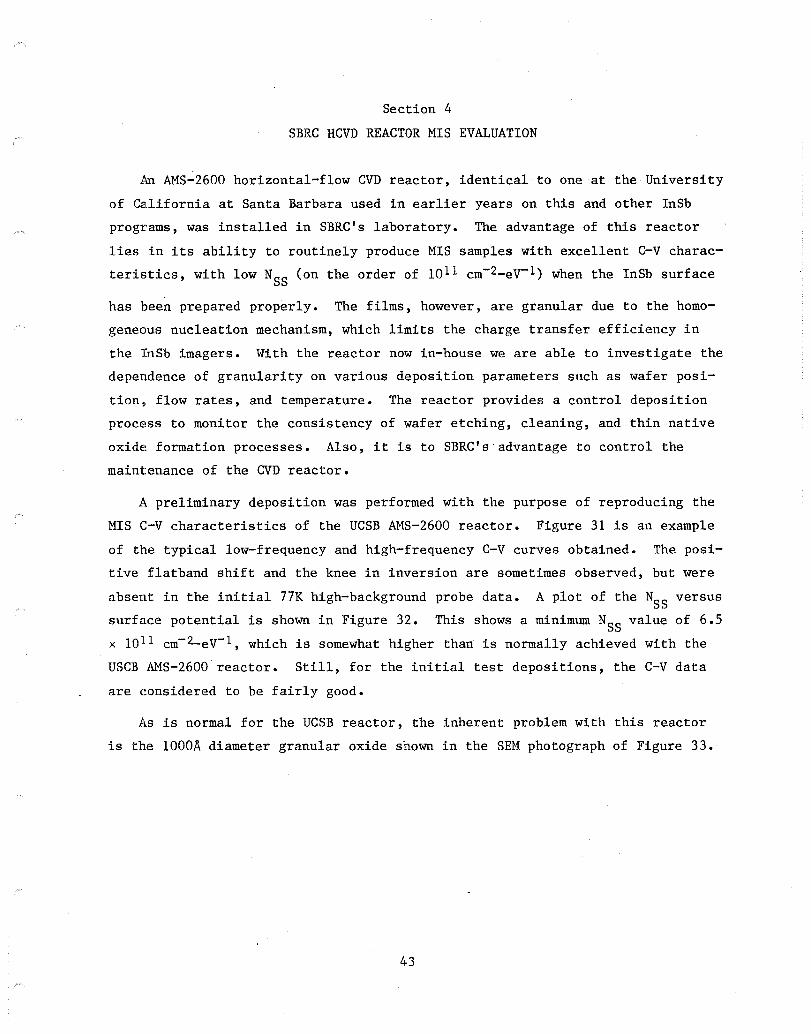
Section 4
SBRC HCVD REACTOR MIS EVALUATION
An AMS-2600 horizontal-flow CVD reactor, identical to one at the University
of California at Santa Barbara used in earlier years on this and other InSb
programs, was installed in SBRC's laboratory. The advantage of this reactor
lies in its ability to routinely produce MIS samples with excellent C-V charac
teristics, with low NSS (on the order of lOll cm-2-eV-l) when the InSb surface
has been prepared properly. The films, however, are granular due to the homo
geneous nucleation mechanism, which limits the charge transfer efficiency in
the TnSb imagers. With the reactor now in-house we are able to investigate the
dependence of granularity on various deposition parameters such as wafer posi
tion, flow rates, and temperature. The reactor provides a control deposition
process to monitor the consistency of wafer etching, cleaning, and thin native
oxide formation processes. Also, it is to SBRC's'advantage to control the
maintenance of the CVD reactor.
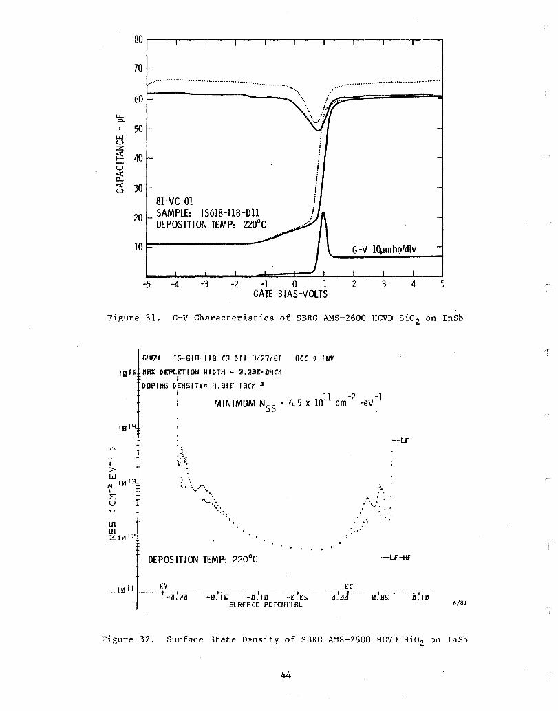
A preliminary deposition was performed with the purpose of reproducing the
MIS C-V characteristics of the UCSB AMS-2600 reactor. Figure 31 is an example
of the typical low-frequency and high-frequency C-V curves obtained. The posi
tive flatband shift and the knee in inversion are sometimes observed, but were
absent in the initial 77K high-background probe data. A plot of the NSS versus
surface potential is shown in Figure 32. This shows a minimum NSS value of 6.5
x lOll cm- 2-eV-l, which is somewhat higher than is normally achieved with the
USCB AMS-2600reactor. Still, for the initial test depositions, the C-V data
are considered to be fairly good.
As is normal for the UCSB reactor, the inherent problem with this reactor
is the 1000A diameter granular oxide shown in the SEM photograph of Figure 33.
43
70
60C----------------u... c..
L.I.J U Z
50
~ 40 u c::( c.. 5 30
20
81-VC-Dl SAMPLE: I S618-118-D11 DEPOSITION TEMP: 220°C
10~--------------~
i 1
f ! ! j
......... /
-5 -4 -3 -2 -1 0 1 GATE BIAS-VOLTS
G-V l~mhQ/div
2 3 4 5
Figure 31. C-V Characteristics of SBRC AMS-2600 HCVD Si02 on InSb
.-I
> W I~ 10 '3 I L: V v
U1 U1 ZIOIi!
6Y6Y IS-6IB-Ila C3 ~II 4/27/BI ACC ~ INV
MAX ~EPlETION UI~rH ~ i!.23E-a4CM I
~OPING ~EN5ITY= 4.Slr 13CM-3 I
MINIMUM NSS
• 6.5 X lOll cm-2 -eV-1
~ ....... ,,.,... ...... . ... '- . . 0.:::.
DEPOS ITION TEMP: 220°C ...
....
... . .' . ........
-If
-If-HF
I I rv rc - ............ ~--I--~o~ .. ~ 2==0:---·-=£1 ~~--i.~ .1!1.*c:1 Elc:::S----:EI""".'"=ol'l::t----I!1.'iiS"--If.'TIl
SUFIFACE pmENJ'I Al 6/81
Figure 32. Surface State Density of SERe AMS-2600 HCVD SiOZ on InSb
44

..... -.:t N I
\0 I
..... ex:>
o G RA INS I ZE: 1000 A
81-VC-01
Sample: IS618-11B
Deposition Temperature: 220°C
Thickness: 1500A
Figure 33. HCVD SiOz Granularity from SBRC AMS-2600 Reactor
45

(THIS PAGE INTENTIONALLY LEFT BLANK)
46
Section 5
SBRC Si02 INVESTIGATIONS
During 1980, several CVD Si02 depositions were performed on a SBRC IR&D
program at the Hughes Aircraft facility in Culver City, California. These
depositions utilized an alternative CVD method to those used previously on this
program. The results of these depositions showed promise of offering an insu
lator with qualities suitable for ultimately achieving a CTE of 0.999. The
films were featureless when inspected with a SEM, and most notably the electri
cal results were uniform from capacitor to capacitor and run to run. The low
est NSS value achieved was 1 x 1012 cm-2-eV-1, but the deposition parameters
were not optimized for InSb, and it was hypothesized this value could be signi
ficantly improved with further investigation.
INITIAL SBRC TEMPERATVRE-FLOW RATE EVALUATION
During April 1981 a similar system became operational at SBRC. As a first
experiment, a matrix investigating various temperatures and flow rates was
initiated in order to determine the dependence on these parameters and to find
a range in which to concentrate. Initially, temperatures were chosen between
200°C and 250°C. However, due to mechanical limitations of the reactor, these
were later changed to range from 150°C to 200°C.
Based on high-frequency C-V results, there is clearly a dependence on tem
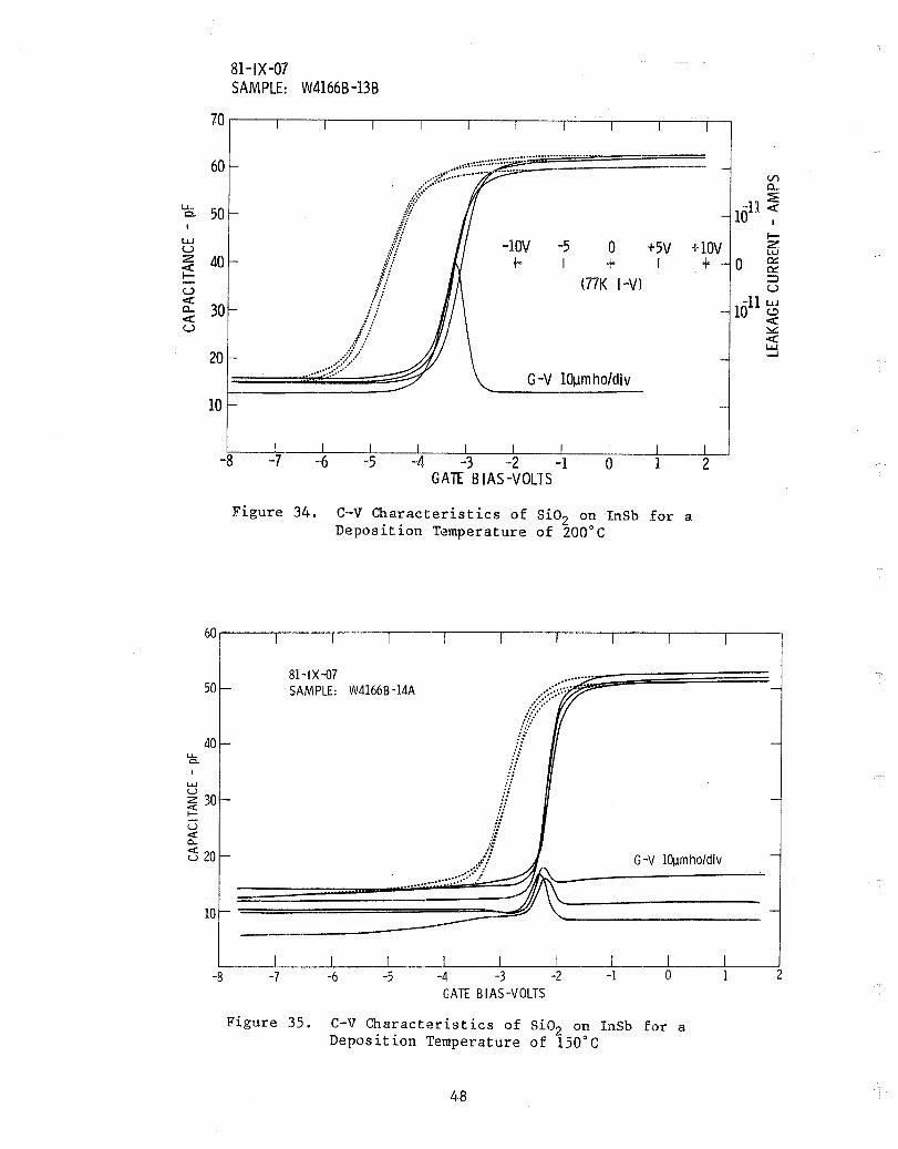
perature and, at a given temperature, on N20/SiH4 ratio. Fig\lres 34 and·35
show C-V curves resulting from depositions at 150°C and 200°C, respectively,
with the flow conditions in each case held constant. When the total flow rate
is increased, the C-V curves are degraded; however, when the flow rates are
changed keeping the N20/SiH4 ratio constant, the C-V curves remain unchanged.
As observed in Figures 34 and 35, the lower deposition temperature resulted in
reduced hysteresis and VFB
.
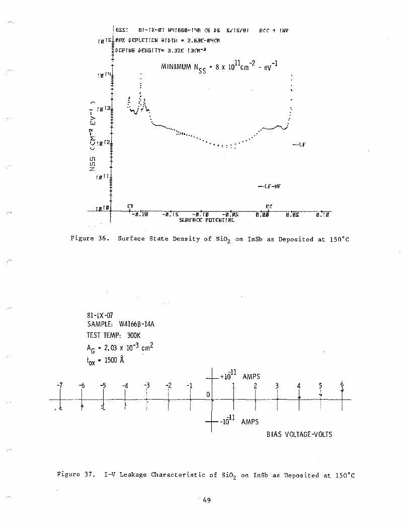
The improved C-V characteristics also resulted in a decrease in the midband
NSS to "'8 x lOll cm2 -eV-l as shown in the curve of Figure 36. The room temper
ature leakage of the oxide was measured as shown in Figure 37. From this test,
the oxide was found to have a resistivity (p) of 1.9 x 10¹⁴ ohm-cm.
47
81-IX -07 SAMPLE: W4166B-13B
70.----.----.----.----.----.----.----,----,----,----r-I
60
~ 50
I..L.I U z 40 ~ u <: 0.. 30 <: u
20
10
o +
(17K I-V)
G-V l(4.lmho/div
+5V I
+lOV +
-8 -7 -6 -5
Figure 34. C-V Characteristics of Si02 on InSh for a Deposition Temperature of 200°C
60~--~----.----,----,---_,----,_--_,r_--_r----r_--~
u... 0.
1..LI
50
40
~ 30 ;:: u oct: c.. (3 20
10
-8
81-IX-07 SAMPLE: W4166B-14A
G -V lOumho/div
Figure 35. C-V Characteristics of Si02 on InSh for a Deposition Temperature of IS0°C
48
2
iEssr S!-fX-07 ~4166B-!4fl (6 DS S/ls/a!
fil ISi ttRX DEPLETION ~flHH ., 2.63E-84(tt
r-_ fBl3 1
> W
I'd I :E V1Bl2 V
U1 U1 Z
Iii
DOP!NS DEN5rTY~ 3.32E !3CM-J
...... -..... •• •• 0 ••
"::'1 00 (>
10 .. , ...... ..
e ... .
€:V
-0.2£1 -fl. r S -fl. I iI -£I. £IS SURfRCE: PDTENTfflL
flce ~ rNV
..
-Lf
-Lf-Hf
E:( £I.iI iI.ilS
Figure 36. Surface State Density of SiOZ on InSb as Deposited at 150°C
-7 -6
+ j
81-IX -07 SAMPLE: W4166B-14A
TEST TEMP: 300K
AG • 2.03 X 10⁻³ cm2
tox • 1500 ~
-5 -4 -3
,l I f
-2 - f- + lOll AMPS
-1 1 2 3 4 5 6 0
- I- -Hlll AMPS
BIAS VOLTAGE-VOLTS
Figu.re 37. I-V Leakage Characteristic of Si02 on loSb as Deposited at 150°C
49

ANNEALING EVALUATION
A second study in which the effects of subjecting the wafers to a post-Si0 2 deposition anneal process (as discussed by Langan 19) waS performed. Figures
38(a) and 38(b), respectively, show the resulting C-V characteristics for ca
pacitors formed on Si02 samples which were unannealed and annealed prior to
deposition of the aluminum capacitors; excluding the sputtered 8i02 layer shown
in Figure 5. As is readily seen, the annealed sample has a flatband which was
shifted from ~(-)1.8 volts to ~(+)0.8 volt. This corresponds to a change in
the fixed charge density (QFC) from (+)3.05 x lOll charges-cm-2 to (-)1.36 x
lOll charges-cm-2• In addition, the hysteresis decreased from a delta of ~.7
volt to <0.2 volt.
An area of concern is observed in the oxide conductance (G-V) peaks. The
annealed sample peak is ~9x greater than the unannealed sample. This charac
teristic proved to be reproducible and is not understood at this time. More
sample tests are required to determine the overall effect of this anomaly.
Finally, although attempts were made to perform quasi-static measurements,
none were obtained which could be used for determining the surface state den
sity.
Si02 GRANULARITY
This method of 8i02 deposition does fulfill the requirement of smooth,
nongranular films. Figure 39 shows a scanning electron micrograph of a 1500A
thick Si02 film deposited on InSb at 150°C. At the magnification shown, very
little structure is discernible. The two visible grains were located for the
purpose of focusing and are not typical of the entire surface.
STORAGE TIME EVALUATION
The final item considered was the ability to obtain measurable storage time
(TS) on MIS samples using this insulator. Figure 40 shows a typical capaci-
tance-time' (C-t) transient obtained from testing these devices. It shows a 90%
TS of ~11 msec. This value is typical of bulk InSb samples with CVD Si0 2 when
tested at 77K. Notably, the storage time was uniform and reproducible from
capacitor to capacitor.
50
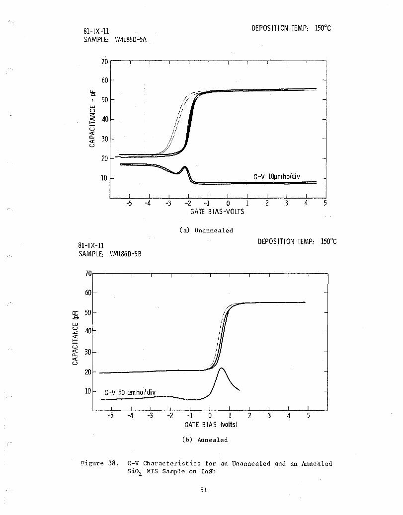
81-IX-ll DEPOS ITiON TEMP: 150°C
SAMPLE: W4I86D-5A
70
60 LL.. 0-
50 LLJ U z
40 <C I-
U <C Cl.. 30 <C U
20
10 ~~==. ======G=-=V=l=O=llm=h=o=/d=iv==
-5 -4 -3 -2 -1 0 1 2 3 5 GATE BIAS-VOLTS
(a) Unannealed
8I-IX-ll DEPOS I TI ON TEMP: 150°C
SAMPLE: W4I86D-5B
u: .,g. LLJ U z <C I-
U <C Cl.. <C U
60
50
40
30
20
10 G-V 50 Ilmho (div
-5 -4 -3 -2 ----
-1 0 1 GATE BIAS (volts)
(b) Annealed
2 3 4 5
Figure 38. C-V Characteristics for an Unannealed and an Annealed Si02 MIS Sample on InSb
51
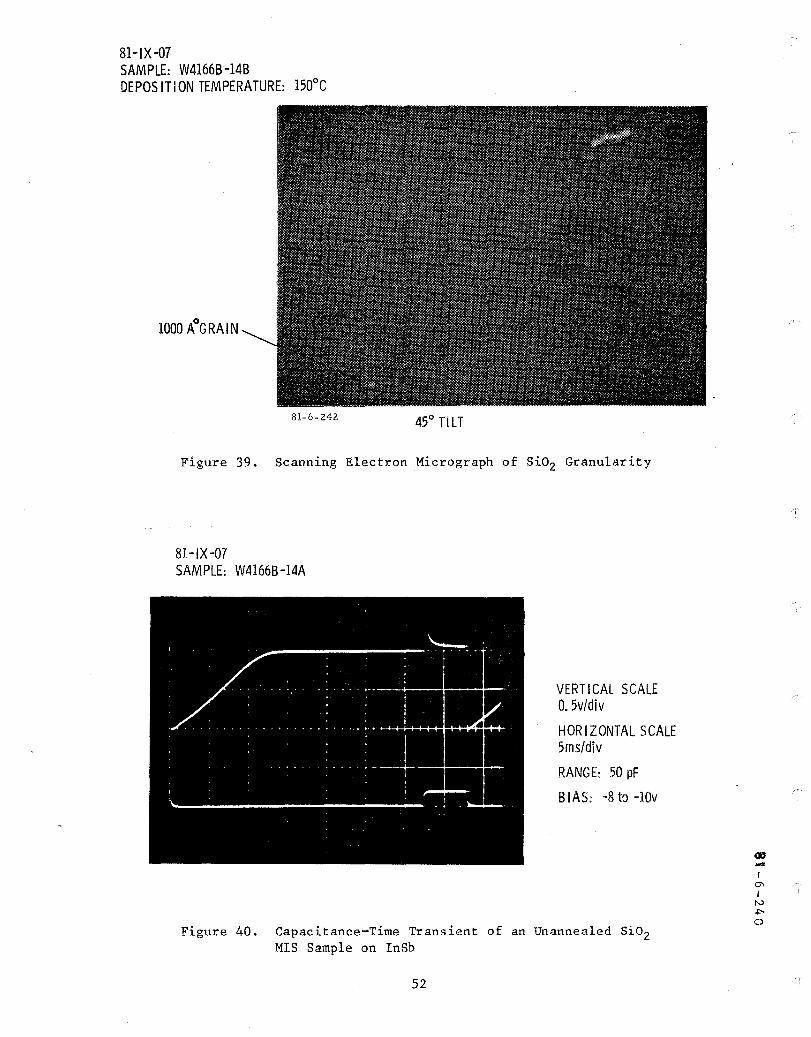
81-IX-07 SAMPLE: W4166B -14B DEPOS ITION TEMPERATURE: 150°C
81-6-242
Figure 39. Scanning Electron Micrograph of Si02 Granularity
81-IX-07 SAMPLE: W4166B-14A
VERTI CAL SCALE 0.5v/div
HORIZONTAL SCALE 5ms/div
RANGE: 50 pF
BIAS: -8 to -lOv
Figure 40. Capacitance-Time Transient of an Unannealed Si02 MIS Sample on InSb
52
0) .... I
0\ I
N ~
o
CONCLUSIONS OF Si02 EVALUATIONS
The results of the investigations, using the SBRC deposited Si02 , show
continued promise of ultimately producing an insulator with interface electri
cal characteristics capable of yielding charge transfer devices with CTE values
)0.999. Although some success was realized by annealing the insulator, as yet
the electrical characteri.stics are not of sufficient quality for use in CCD
fabrication. Considerably more investigative work will be required to develop
a process which can routinely produce insulators with NSS values in the re
quired range (~1011 cm-2-eV-1).
53

(THIS PAGE INTENTIONALLY LEFT BLANK)
54

Section 6
SUMMARY
This report has discussed the efforts pursued in attempting to develop
advanced indium antimonide (InSb) monolithic charge-coupled infrared imaging
arrays.
The objective of the first task of this program effort was to fabricate a
gate oxide with the electrical and physical properties necessary to achieve a
charge transfer efficiency (CTE) of 0.999 or greater with InSb IRCCD imagers;
that is, to achieve improved performance compared to lnSb imagers previously
fabricated and delivered to NASA LRC (which displayed a CTE --D.995). The basic
technical approach was to utilize a plasma enhanced chemical vapor deposition
(PECVD) process to deposit the gate oxide. This approach was supplemented
later in the effort by investigations of (1) horizontal CVD (HCVD) with the
addition of HCI gas, (2) an in-house HCVD AMS-2600 system process, and (3) a
third SBRC 8i02 process.
The PECVD Si02 process was pursued as the basic approach in order to reduce
or eliminate the physical granularity of the gate oxide films, which had been
corrE~lated with the lower-than-desired CTEs of the earlier-developed imaging
devices. As to this goal, the PECVD process was very successful; operational
parameters were established for deposition of smooth, essentially-featureless
Si02 films when examined by scanning electron microscopy (SEM). Encouragingly,
samples with excellent MIS characteristics were also produced early-on in the
PECVD investigation, displaying, in fact, better electrical properties than
ever before reported for InSb. Unfortunately, although many extensive experi
ments were carried out with the best control possible over the deposition and
system variables, the PECVD Si02 gate oxide was found to be nonreproducible
from run to run, as well as nonuniform over the InSb wafer surface in a given
deposition. Reactant gas premixing was displaying some progress toward the end
of the effort in improving the spatial uniformity; however, electrical charac
teristics and other gate oxide quality measures remained unpredictable over
wide limits from one deposition to the next.
In summary, at the conclusion of the gate oxide development effort, the
PECVD process was incapable of reliably producing the electrical properties
necessary to achieve a CTE of 0.999 when utilized for InSb imager fabrication.
55
It was concluded that rectifying this situation would necessitate rather major
redesign of the LFE PECVD system, modifying the gas dispersion components,
introducing platen rotation, and making other changes. The alternative method
(3) mentioned earlier was in fact found to show more promise, producing non
granular and highly uniform 8i02 gate oxides; however, the electrical charac
teristics achieved by the end of the effort were as yet inadequate for achiev
ing a CTE of 0.999.
56

REFERENCES
1. R.D. Thorn, R.E. Eck, J.D. Phillips, and J.B. Scorso, "InSb CCDs and Other MIS Devices for Infrared Applications," Proc. of the 1975 IntI. Conf. on the Applications of CCDs, San Diego, CA, 29-31 Oct. 1975.
2. J.D. Phillips, J.B. Scorso, and R.D. Thorn, "InSb Arrays with CCD Readout for 1.0- to 5.5-l1m IR Applications," Proc. of the 1976 NASA-JPL Symposium on CCD Technology and Applications, October 1976.
3. R.D. Thorn, T.L. Koch, W.J. Parrish, J.D. Langan, and S.C. Chase, "InSb Charge Coupled Infrared Imaging Device - 20-Element Linear Imager," NASA Contractor Report 3235, Contract NASl-14922, February 1980.
4. T.L. Koch, R.D. Thorn, and W.J. Parrish, "Advanced InSb Monolithic Charge Coupled Infrared Imaging Devices (CCIRID)," NASA Contractor Report 165766, Contract NASl-15551, April 1981.
5. R.D. Thorn, T.L. Koch, J.D. Langan, and W.J. Parrish, "A Fully Monolithic lnSb Infrared CCD Array," IEEE Transactions on Electron Devices, Volume ED-27, No.1 (ISSN 0018-9383), January 1980, pp. 160-170.
6. R.D. Thorn, W.J. Parrish, and T.L. Koch, "Monolithic InSb CCD Array Technology," Proc. of the IRIS Infrared Detector Specialty Group Meeting, Minneapolis, MN, 12-13 June 1979.
7. J.D. Phillips and R.E. Eck, "Development of InSb Charge-Coupled Infrared Imaging Device - Linear Imager," NASA Contractor Report 145003, Contract NASl-13937, 1 April 1976, pp. 4-1 to 5-2.
8. J.D. Langan, "Study and Characterization of Semiconductor Surfaces and Interfaces," PhD Dissertation, No. 80-19842, University of California at Santa Barbara, July 1979.
9. J.D. Langan, C.R. Viswanathan, R.D. Thorn, C.A. Merilainen, and R.E. Kvaas, "Characterization of Improved InSb Interfaces," Sixth Annual Conference on the Physics of Compound Semiconductor Interfaces, 30 January-1 February 1979" Asilomar Conf. Grounds, Pacific Grove, CA.
10. J.D. Langan, C.R. Viswanathan, C.A. Merilainen, and J.F. Santarosa, "Characterization of Improved InSb Interfaces," IEEE IntI. Electron Devices Meeting Technical Digest, Washington, D.C., December 1978.
11. Ope cit. , Reference 3.
12. Ope cit. , Reference 9.
13. Ope cit. , Reference 3.
14. M. Zerbst and Z •• Angew , Phys. 22. 30 (1966) • -15. Ope cit. , Reference 9.
57

16. Robert W. Loser and Donald T. Larson, RFP-1392, Oct. 1969, "A FORTRAN IV Program for Ellipsometer Measurements of Surface Films," Rockwell Instructional Rocky Flats Division, Golden, CO, report for U.S. Atomic Energy Commission, under Contract AT(29-1)-1106 (Dow Chemical operated the facility at the time of the report, currently available from Rockwell Instructional at Golden, CO).
17. D. Fritzshe, Elec. Lett. li, 51-2 (1978).
18. A.K. Gaind and L.A. Kasprzak, Solid-State Elect. ~, 303-309 (1979).
19. Ope cit., Reference 9.
58
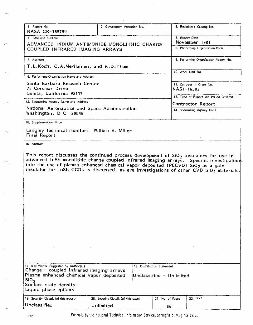
1. Report No.
NASA CR-165799 I 2. Government Accession No.
4. Title and Subtitle
ADVANCED INDIUM ANTIMONIDE MONOLITHIC CHARGE COUPLED INFRARED IMAGING ARRAYS
7. Author(s)
T. L. Koch, C .A.Meriiainen, and R. D. Thorn
9. Performing Organization Name and Address
Santa Barbara Reseach Center 7S Coromar Drive Goleta, California 93117
12. Sponsoring Agency Name and Address
National Aeronautics and Space Administration Washington, D C 20546
15. Supplementary Notes
Langley technical monitor: William E. Miller Final Report
16. Abstract
3. Recipient's Catalog No.
5. Report Date
November 1981 6. Performing Organization Code
8. Performing Organization Report No.
10. Work Unit No.
11. Contract or Grant No.
NAS1-16383
13. Type of Report and Period Covered
Contractor Report 14. Sponsoring Agency Code
This report discusses the continued process development of Si0 2 insulators for use in advanced InSb monolithic charge-coupled infrared imaging arrays. Specific investigation~ into the use of plasma enhanced chemical vapor deposited (PECVD) Si02 as a gate insulator for InSb CCDs is discussed, as are investigations of other CVD Si02 materials.
17. Key Words (Suggested by Author(s)) Charge - coupled infrared imaging arrays Plasma enhanced chemical vapor deposited Si0 2 Surface state density Liquid phase epitaxy
18. Distribution Statement
Unclassified - Unlimited
19. Security Classif. (of this report)
Unclassified
20. Security Classif. (of this page)
Unlimited
21. No. of Pages
66
22. Price
N-305 For sale by the National Technical Information Service, Springfield, Virginia 22161

(THIS PAGE INTENTIONALLY LEFT BLANK)

End of Document