Momentum and Impulse 1 Momentum What does it mean to have momentum? 2.

Advanced Design System 2001
Momentum
August 2001

iii
Contents1 Momentum Basics
Momentum Major Benefits ................................................................................. 1-1Momentum Major Features ................................................................................ 1-1
Momentum Overview................................................................................................ 1-2About the Simulation Modes..................................................................................... 1-4
Selecting the Correct Mode................................................................................ 1-5Locating Example Projects ....................................................................................... 1-7
2 Getting Started with MomentumLayout Basics ........................................................................................................... 2-1
Creating a Layout from a Complete Schematic .................................................. 2-2Creating a Layout Directly .................................................................................. 2-5Shapes ............................................................................................................... 2-6Layers................................................................................................................. 2-7
Designing a Microstrip Line ...................................................................................... 2-13Drawing the Circuit ............................................................................................. 2-13Creating a Simple Substrate............................................................................... 2-20Setting up Mesh Parameters .............................................................................. 2-23Performing the Simulation .................................................................................. 2-25
Designing a Microstrip Filter ..................................................................................... 2-27Drawing the Circuit ............................................................................................. 2-27Generating the Layout ........................................................................................ 2-30Defining a Substrate ........................................................................................... 2-31Adding Ports to the Layout ................................................................................. 2-33Finishing the Box around the Filter..................................................................... 2-35Generating a Mesh............................................................................................. 2-36Performing the Simulation .................................................................................. 2-37Viewing Simulation Results ................................................................................ 2-39
Designing a Coplanar Waveguide Bend................................................................... 2-39Creating the Layout ............................................................................................ 2-40Opening a Substrate........................................................................................... 2-45Adding Ports ....................................................................................................... 2-46Generating the Mesh.......................................................................................... 2-48Performing a Simulation ..................................................................................... 2-49Viewing Simulation Results ................................................................................ 2-50
3 SubstratesSelecting a Predefined Substrate ............................................................................. 3-2Reading a Substrate Definition from a Schematic.................................................... 3-3Saving a Substrate ................................................................................................... 3-3

iv
Identifying Where Substrates are Saved ............................................................ 3-4Creating/Modifying a Substrate ................................................................................ 3-4Changing Substrates ................................................................................................ 3-4Deleting a Substrate ................................................................................................. 3-4Defining Substrate Layers ........................................................................................ 3-5
Defining an Open Boundary ............................................................................... 3-6Defining an Interface Layer................................................................................. 3-7Defining a Closed Boundary Layer..................................................................... 3-9Renaming a Layer .............................................................................................. 3-10Deleting, Adding, and Moving Layers ................................................................. 3-10Defining Silicon Substrate Layers....................................................................... 3-11
Defining Metallization Layers.................................................................................... 3-12Mapping a Layout Layer ..................................................................................... 3-14Unmapping a Layer ............................................................................................ 3-15Defining Conductivity.......................................................................................... 3-15Setting Overlap Precedence............................................................................... 3-16
Precomputing the Substrate Function ...................................................................... 3-18Viewing Substrate Computation Status .............................................................. 3-19
Stopping Substrate Computations............................................................................ 3-19Viewing the Substrate Summary .............................................................................. 3-19Reusing Substrate Calculations ............................................................................... 3-20About Dielectric Parameters ..................................................................................... 3-21
Dielectric Permittivity .......................................................................................... 3-21Dielectric Loss Tangent ...................................................................................... 3-22Dielectric Conductivity ........................................................................................ 3-22Dielectric Relative Permeability .......................................................................... 3-23Dielectric Magnetic Loss Tangent....................................................................... 3-24
Substrate Definition Summary.................................................................................. 3-25Substrate Examples ................................................................................................. 3-25
Substrate for Radiating Antennas....................................................................... 3-26377 Ohm Terminations and Radiation Patterns.................................................. 3-26Substrate for Designs with Air Bridges ............................................................... 3-26
Applying Vias............................................................................................................ 3-29
4 PortsAdding a Port to a Circuit.......................................................................................... 4-1
Considerations.................................................................................................... 4-1Determining the Port Type to Use............................................................................. 4-2Defining a Single Port............................................................................................... 4-4
Avoiding Overlap ................................................................................................ 4-6Applying Reference Offsets................................................................................ 4-6Allowing for Coupling Effects .............................................................................. 4-9

v
Defining an Internal Port........................................................................................... 4-10Defining a Differential Port........................................................................................ 4-12Defining a Coplanar Port .......................................................................................... 4-14Defining a Common Mode Port ................................................................................ 4-17Defining a Ground Reference................................................................................... 4-18Editing a Port ............................................................................................................ 4-19Remapping Port Numbers ........................................................................................ 4-20
5 Boxes and WaveguidesAdding a Box ............................................................................................................ 5-2
Editing a Box ...................................................................................................... 5-3Deleting a Box .................................................................................................... 5-3Viewing Layout Layer Settings of a Box ............................................................. 5-3
Adding a Waveguide................................................................................................. 5-4Editing a Waveguide........................................................................................... 5-4Deleting a Waveguide......................................................................................... 5-4Viewing Layout Layer Settings of a Waveguide.................................................. 5-5
About Boxes and Waveguides.................................................................................. 5-5Adding Absorbing Layers under a Cover............................................................ 5-6Boxes, Waveguides, and Radiation Patterns...................................................... 5-6
6 MeshDefining a Mesh........................................................................................................ 6-2
Defining Mesh Parameters for the Entire Circuit ................................................ 6-2Defining Mesh Parameters for a Layout Layer.................................................... 6-4Defining Mesh Parameters for an Object............................................................ 6-5Seeding an Object .............................................................................................. 6-6Resetting and Clearing Mesh Parameters.......................................................... 6-10
Precomputing a Mesh............................................................................................... 6-11Viewing Mesh Status .......................................................................................... 6-11
Stopping Mesh Computations .................................................................................. 6-12Viewing the Mesh Summary..................................................................................... 6-12Clearing a Mesh ....................................................................................................... 6-13About the Mesh Generator ....................................................................................... 6-13
Adjusting Mesh Density ...................................................................................... 6-14About the Edge Mesh......................................................................................... 6-15About the Transmission Line Mesh..................................................................... 6-16Combining the Edge and Transmission Line Meshes......................................... 6-16Mesh Patterns and Simulation Time................................................................... 6-18Mesh Patterns and Memory Requirements........................................................ 6-19Using the Arc Facet Angle.................................................................................. 6-19Processing Object Overlap................................................................................. 6-21Mesh Generator Messages ................................................................................ 6-22

vi
Guidelines for Meshing............................................................................................. 6-23Meshing Thin Layers .......................................................................................... 6-23Meshing Thin Lines ............................................................................................ 6-23Meshing Slots..................................................................................................... 6-24Adjusting the Mesh Density of Curved Objects .................................................. 6-24Discontinuity Modeling........................................................................................ 6-24Solving Tightly Coupled Lines ............................................................................ 6-25Editing Object Seeding....................................................................................... 6-25Mesh Precision and Gap Resolution .................................................................. 6-25
7 SimulationSetting Up a Frequency Plan.................................................................................... 7-2
Considerations.................................................................................................... 7-3Editing Frequency Plans..................................................................................... 7-3
Selecting a Process Mode........................................................................................ 7-4Reusing Simulation Data .......................................................................................... 7-5Saving Simulation Data ............................................................................................ 7-5
Saving Data for Export ....................................................................................... 7-6Viewing Results Automatically.................................................................................. 7-6Starting a Simulation ................................................................................................ 7-7
Viewing Simulation Status .................................................................................. 7-7Stopping a Simulation............................................................................................... 7-8Viewing the Simulation Summary............................................................................. 7-9Performing Remote Simulations ............................................................................... 7-13
UNIX to UNIX ..................................................................................................... 7-14PC to PC ............................................................................................................ 7-17
About Adaptive Frequency Sampling ....................................................................... 7-20AFS Convergence .............................................................................................. 7-21Setting Sample Points ........................................................................................ 7-22Viewing AFS S-parameters ................................................................................ 7-23
8 Radiation Patterns and Antenna CharacteristicsAbout Radiation Patterns.......................................................................................... 8-1About Antenna Characteristics ................................................................................. 8-2
Polarization......................................................................................................... 8-2Radiation Intensity .............................................................................................. 8-4Radiated Power .................................................................................................. 8-4Effective Angle.................................................................................................... 8-4Directivity ............................................................................................................ 8-5Gain.................................................................................................................... 8-5Efficiency ............................................................................................................ 8-5Effective Area ..................................................................................................... 8-5
Calculating Radiation Patterns ................................................................................. 8-6

vii
Planar (Vertical) Cut ........................................................................................... 8-8Conical Cut ......................................................................................................... 8-8
Viewing Results Automatically in Data Display......................................................... 8-9Exporting Far-Field Data .......................................................................................... 8-9
9 Viewing Results Using the Data DisplayOpening a Data Display Window.............................................................................. 9-1Viewing Momentum Data ......................................................................................... 9-2Viewing S-parameters .............................................................................................. 9-4
Variables in the Standard and AFS Dataset ....................................................... 9-4Standard and AFS Datasets............................................................................... 9-5Viewing Convergence Data ................................................................................ 9-5
Viewing Radiation Patterns....................................................................................... 9-9Variables in the Far-field Dataset........................................................................ 9-9
10 Momentum Visualization BasicsStarting Momentum Visualization............................................................................. 10-1Working with Momentum Visualization Windows ..................................................... 10-2
Selecting the Number of Views .......................................................................... 10-3Selecting a View to Work in................................................................................ 10-4Setting Preferences for a View ........................................................................... 10-5Working with Annotation in a View ..................................................................... 10-6Retrieving Plots in a View................................................................................... 10-8Refreshing the Window ...................................................................................... 10-8
Data Overview .......................................................................................................... 10-8Working with Plots and Data .................................................................................... 10-9
Displaying a Plot................................................................................................. 10-9Adding Data to a Displayed Plot ......................................................................... 10-10Working with Data Controls ................................................................................ 10-11Viewing Data from Another Project .................................................................... 10-12Erasing Data from a Plot .................................................................................... 10-13Reading Data Values from a Plot ....................................................................... 10-13Working with Plot Controls ................................................................................. 10-14Working with Rectangular-plot Editing Controls ................................................. 10-15
Saving a Plot ............................................................................................................ 10-18Importing a Plot ........................................................................................................ 10-20
11 Displaying S-parametersS-parameter Overview.............................................................................................. 11-1
Normalization Impedance................................................................................... 11-1Naming Convention ............................................................................................ 11-1
Viewing S-parameters in Tabular Format ................................................................. 11-1Plotting S-parameter Magnitude............................................................................... 11-3
viii
Plotting S-parameter Phase ..................................................................................... 11-3Plotting S-parameters on a Smith Chart................................................................... 11-5Exporting S-parameters ........................................................................................... 11-6
12 Displaying Surface CurrentsSetting Port Solution Weights ................................................................................... 12-1Displaying the Layout ............................................................................................... 12-1Displaying a Current Plot .......................................................................................... 12-2
Animating Plotted Currents ................................................................................ 12-3Displaying the Mesh on a Current Plot ..................................................................... 12-4
13 Displaying Radiation ResultsLoading Radiation Results........................................................................................ 13-1Displaying Far-fields in 3D........................................................................................ 13-2
Selecting Far-field Display Options..................................................................... 13-3Defining a 2D Cross Section of a Far-field ............................................................... 13-3Displaying Far-fields in 2D........................................................................................ 13-5Displaying Antenna Parameters ............................................................................... 13-6
14 Displaying Transmission Line DataViewing Transmission Data....................................................................................... 14-2Displaying Gamma on a Plot .................................................................................... 14-2Displaying an Impedance Plot .................................................................................. 14-3
15 Momentum OptimizationWhat can be optimized by Momentum Optimization? .............................................. 15-1
What cannot be optimized by Momentum Optimization? ................................... 15-2What responses can be optimized by Momentum Optimization?....................... 15-2
Typical steps in using Momentum Optimization........................................................ 15-2The Optimization Process .................................................................................. 15-3When Optimization is Finished........................................................................... 15-4Restarting Optimization ...................................................................................... 15-5
Working with Optimization Parameters..................................................................... 15-5Parameters (list) ................................................................................................. 15-6Parameter Definition........................................................................................... 15-6
Using Advanced Parameter Settings........................................................................ 15-8Adding Parameters to Designs ................................................................................. 15-10
Editing Parameters ............................................................................................. 15-11Verifying Your Changes ...................................................................................... 15-12Viewing and Editing Your Design........................................................................ 15-13
Working with Optimization Goals.............................................................................. 15-14Edit/Define Goal box........................................................................................... 15-14Defining a Goal................................................................................................... 15-15
Performing an Optimization ...................................................................................... 15-16

ix
Setting Optimization Controls ............................................................................. 15-17Starting an Optimization ..................................................................................... 15-18
Viewing Optimization Status..................................................................................... 15-19Viewing Optimization Results ................................................................................... 15-20Example - Optimizing a Microstrip Line .................................................................... 15-23
Step 1: Creating the Project and Layout............................................................. 15-23Step 2: Defining the Optimized Parameters ....................................................... 15-25Step 3: Defining Optimization Goals .................................................................. 15-29Step 4: Running the Optimization....................................................................... 15-30Step 5: Viewing Optimization Results................................................................. 15-32
Example - Optimizing a Filter ................................................................................... 15-33Step 1: Creating the Initial Layout ...................................................................... 15-34Step 2: Defining the Optimized Parameters ....................................................... 15-35Step 3: Defining Optimization Goals .................................................................. 15-38Step 4: Running the Optimization....................................................................... 15-40Step 5: Viewing Optimization Results................................................................. 15-41
A Theory of OperationThe Method of Moments Technology ....................................................................... A-2The Momentum Solution Process ............................................................................ A-6
Calculation of the Substrate Green's Functions ................................................. A-6Meshing of the Planar Signal Layer Patterns ..................................................... A-7Loading and Solving of the MoM Interaction Matrix Equation ............................ A-7Calibration and De-embedding of the S-parameters .......................................... A-8Reduced Order Modeling by Adaptive Frequency Sampling.............................. A-8
Special Simulation Topics......................................................................................... A-9Simulating Slots in Ground Planes..................................................................... A-9Simulating Metallization Loss ............................................................................. A-10
Simulating with Internal Ports and Ground References............................................ A-10Internal Ports and Ground Planes in a PCB Structure ....................................... A-12Finite Ground Plane, no Ground Ports ............................................................... A-13Finite Ground Plane, Internal Ports in the Ground Plane ................................... A-15Finite Ground Plane, Ground References .......................................................... A-17Internal Ports with a CPW Structure................................................................... A-19
Limitations and Considerations ................................................................................ A-21Comparing the Microwave and RF Simulation Modes........................................ A-22Matching the Simulation Mode to Circuit Characteristics ................................... A-23Higher-order Modes and High Frequency Limitation.......................................... A-25Interpolating Results below the Low Frequency Limitation ................................ A-25Parallel Plate Modes........................................................................................... A-26Surface Wave Modes ......................................................................................... A-27Slotline Structures and High Frequency Limitation............................................. A-27

x
Via Structures and Metallization Thickness Limitation ....................................... A-28Via Structures and Substrate Thickness Limitation ............................................ A-28CPU Time and Memory Requirements .............................................................. A-28
B Drawing TipsUsing Grid Snap Modes ........................................................................................... B-1Choosing Layout Layers ........................................................................................... B-1Keeping Shapes Simple ........................................................................................... B-1Merging Shapes ....................................................................................................... B-2Viewing Port and Object Properties.......................................................................... B-2Using Layout Components ....................................................................................... B-2Drawing Coplanar Waveguide in Layout .................................................................. B-3Adding a Port to a Circuit.......................................................................................... B-4
Adding a Port to a Schematic ............................................................................. B-4Adding a Port to a Layout ................................................................................... B-5Considerations.................................................................................................... B-7
Drawing Vias in Layout ............................................................................................. B-8Vias through Multiple Substrate Layers .............................................................. B-10
Using Vias to Model Finite Thickness....................................................................... B-11Drawing Air Bridges in Layout .................................................................................. B-12Ports and Air Bridges in Coplanar Designs .............................................................. B-12
C Exporting Momentum DataExporting Momentum Data to IC-CAP ..................................................................... C-1
Enabling the IC-CAP MDM File Output .............................................................. C-1Disabling the IC-CAP MDM File Output ............................................................. C-1Example ............................................................................................................. C-2
Exporting Momentum Data to Agilent HFSS ............................................................ C-3
D Momentum Optimization - Background InformationOptimization Variables.............................................................................................. D-1Design Goals/Specifications..................................................................................... D-2How Design Goals are used by the Optimizers ........................................................ D-4Optimization Algorithms............................................................................................ D-6Stopping Criteria for the Optimization Process......................................................... D-7
E Momentum Optimization - Response InterpolationInterpolation Grid and Resolution............................................................................. E-1How Does the Interpolation Feature Work? ............................................................. E-2Actual EM Simulations and Database ...................................................................... E-3Removing Obsolete Databases................................................................................ E-3Hints for Selecting the Interpolation Resolution........................................................ E-4Zero Parameter Values............................................................................................. E-5The Impact of Parameter Bounds on Interpolation................................................... E-6

xi
“No interpolation” Option .......................................................................................... E-7Interpolation in Gradient Evaluation ......................................................................... E-7Types of Interpolation ............................................................................................... E-8
Linear Interpolation............................................................................................. E-8Quadratic Interpolation ....................................................................................... E-9
F Momentum Optimization - Layout ParameterizationGuidelines for Preparing Perturbed Designs ............................................................ F-2Vias Parameterization............................................................................................... F-3
G Command ReferenceIndex

xii

1-1
Chapter 1: Momentum BasicsMomentum is a part of Advanced Design System and gives you the simulation toolsyou need to evaluate and design modern communications systems products.Momentum is an electromagnetic simulator that computes S-parameters for generalplanar circuits, including microstrip, slotline, stripline, coplanar waveguide, andother topologies. Vias and airbridges connect topologies between layers, so you cansimulate multilayer RF/microwave printed circuit boards, hybrids, multichipmodules, and integrated circuits. Momentum gives you a complete tool set to predictthe performance of high-frequency circuit boards, antennas, and ICs.
Momentum Optimization extends Momentum capability to a true design automationtool. The Momentum Optimization process varies geometry parametersautomatically to help you achieve the optimal structure that meets the circuit ordevice performance goals.
Momentum Visualization is an option that gives users a 3-dimensional perspective ofsimulation results, enabling you to view and animate current flow in conductors andslots, and view both 2D and 3D representations of far-field radiation patterns.
If you are unfamiliar with Advanced Design System, refer to the Quick Tour in theonline documentation, and to the User’s Guide. To learn how to create a physicaldesign, refer to Layout. For information on the interactions between Layout andMomentum, refer to Appendix B, Drawing Tips.
Momentum Major Benefits
Momentum enables you to:
• Simulate when a circuit model range is exceeded or the model does not exist
• Identify parasitic coupling between components
• Go beyond simple analysis and verification to design automation of circuitperformance
• Visualize current flow and 3-dimensional displays of far-field radiation
Momentum Major Features
Key features of Momentum include:
• An electromagnetic simulator based on the Method of Moments
1-2 Momentum Overview
Momentum Basics
• Adaptive frequency sampling for fast, accurate, simulation results
• Optimization tools that alter geometric dimensions of a design to achieveperformance specifications
• Comprehensive data display tools for viewing results
• Equation and expression capability for performing calculations on simulateddata
Momentum OverviewMomentum commands are available from the Layout window. The following stepsdescribe a typical process for creating and simulating a design with Momentum:
1. Create a physical design . You start with the physical dimensions of a planardesign, such as a patch antenna or the traces on a multilayer printed circuitboard. There are three ways to enter a design into Advanced Design System:
• Convert a schematic into a physical layout
• Draw the design using Layout
• Import a layout from another simulator or design system. Advanced DesignSystem can import files in a variety of formats.
For information on converting schematics or drawing in Layout, refer to theLayout manual. For information on importing designs, refer to the manual,Importing and Exporting Designs.
2. Choose Momentum or Momentum RF mode. Momentum can operate in twosimulation modes: microwave or RF. You can select the mode based on yourdesign goals. Use Momentum (microwave) mode for designs requiring full-waveelectromagnetic simulations that include microwave radiation effects. UseMomentum RF mode for designs that are geometrically complex, electricallysmall, and do not radiate. You might also choose Momentum RF mode for quicksimulations on new microwave models that can ignore radiation effects, and toconserve computer resources. For more information comparing the Momentumand Momentum RF modes, see “About the Simulation Modes” on page 1-4.

Momentum Overview 1-3
3. Define the substrate characteristics. A substrate is the media upon which thecircuit resides. For example, a multilayer PC board consists of various layers ofmetal, insulating or dielectric material, and ground planes. Other designs mayinclude covers, or they may be open and radiate into air. A complete substratedefinition is required in order to simulate a design. The substrate definitionincludes the number of layers in the substrate and the composition of eachlayer. This is also where you position the layers of your physical design withinthe substrate, and specify the metal characteristics of these layers. For moreinformation, refer to the chapter, Chapter 3, Substrates.
4. Solve the substrate. Momentum calculates the Green’s functions thatcharacterize the substrate for a specified frequency range. These calculationsare stored in a database, and used later on in the simulation process. For moreinformation, refer to Chapter 3, Substrates.
5. Assign port properties. Ports enable you to inject energy into a circuit, which isnecessary in order to analyze the behavior of your circuit. You apply ports to acircuit when you create the circuit, and then assign port properties inMomentum. There are several different types of ports that you can use in yourcircuit, depending on your application. For more information, refer to Chapter4, Ports.
6. Add a box or a waveguide. These elements enable you to specify boundaries onsubstrates along the horizontal plane. Without a box or waveguide, thesubstrate is treated as being infinitely long in the horizontal direction. Thistreatment is acceptable for many designs, but there may be instances where aboundaries need to be taken into account during the simulation process. A boxspecifies the boundaries as four perpendicular, vertical walls that make a boxaround the substrate. A waveguide specifies two vertical walls that cut twosides of the substrate. For more information, refer to Chapter 5, Boxes andWaveguides.
7. Set up and generate a circuit mesh. A mesh is a pattern of rectangles andtriangles that is applied to a design in order to break down (discretize) thedesign into small cells. A mesh is required in order to simulate the designeffectively. You can specify a variety of mesh parameters to customize the meshto your design, or use default values and let Momentum generate an optimalmesh automatically. For more information, refer to Chapter 6, Mesh.

1-4 About the Simulation Modes
Momentum Basics
8. Simulate the circuit . You set up a simulation by specifying the parameters of afrequency plan, such as the frequency range of the simulation and the sweeptype. When the setup is complete, you run the simulation. The simulationprocess uses the Green’s functions computed for the substrate, plus the meshpattern, and the currents in the design are calculated. S-parameters are thencomputed based on the currents. If the Adaptive Frequency Sample sweep typeis chosen, a fast, accurate simulation is generated, based on a rational fit model.For more information, refer to Chapter 7, Simulation.
9. View the results. The data from an Momentum simulation is saved asS-parameters or as fields. Use the Data Display or Visualization to viewS-parameters and far-field radiation patterns. For more information, refer toChapter 9, Viewing Results Using the Data Display and Chapter 10,Momentum Visualization Basics.
About the Simulation ModesWith ADS 1.5, Momentum added an RF simulation mode to its existing microwavemode. The microwave mode is called Momentum; the new RF mode is calledMomentum RF. Momentum RF provides accurate electromagnetic simulationperformance at RF frequencies, typically up to 10 GHz; however, this upper limitdepends on the size of your physical design. At higher frequencies, as radiationeffects increase, the accuracy of the Momentum RF models declines smoothly withincreased frequency. Momentum RF addresses the need for faster, more stablesimulations down to DC, while conserving computer resources. Typical RFapplications include RF components and circuits on chips, modules, and boards, aswell as digital and analog RF interconnects and packages.
When compared to the Momentum mode, the Momentum RF mode uses newtechnologies enabling it to simulate physical designs at RF frequencies with severaluseful benefits. The RF mode is based on quasi-static electromagnetic functionsenabling faster simulation of designs. The star-loop technology provideslow-frequency stability down to DC. The mesh-reduction algorithms allow quicksimulation of complex designs, and require less computer memory and CPU time.Additionally, Momentum RF has the same use-model as Momentum in ADS, andworks with Momentum Visualization and Optimization. The following table showshow each mode supports Momentum product features. For a detailed comparison of

About the Simulation Modes 1-5
the two simulation modes, see “Comparing the Microwave and RF Simulation Modes”on page A-22.:
Selecting the Correct Mode
In the Layout window, the Momentum menu label displays the current simulationmode. To select the mode, toggle the mode setting.
• To switch the mode from Momentum to Momentum RF, choose Momentum >Enable RF Mode .
• To switch the mode from Momentum RF to Momentum, choose Momentum RF >Disable RF Mode .
In each case, the menu label in the Layout window changes to the current mode.
Deciding which mode to use depends on your application. Each mode has itsadvantages. In addition to specifically RF applications, Momentum RF can simulatemicrowave circuits. The following graph identifies which mode is best suited forvarious applications. As you can see, some applications can benefit from using eithermode depending on your requirements. As your requirements change, you canquickly switch modes to simulate the same physical design. As an example, you maywant to begin simulating microwave applications using Momentum RF for quick,
Table 1-1. Features Supported in Momentum and Momentum RF Modes
Feature Momentum Mode Momentum RF Mode
Substrate Database Yes Yes
Functions Fullwave Quasi-static
Ports Port Types Yes Yes
Calibration Yes No
Box Waveguide Yes No
Mesh Mesh Options Yes Yes
Cells Rectangle / Triangle Polygonal
Simulation Sweep Types Yes Yes
Base Functions Rooftop Star/Loop
Optimization Yes Yes
PostProcessing
Visualization Yes Yes
Radiation Pattern Yes No

1-6 About the Simulation Modes
Momentum Basics
initial design and optimization iterations, then switch to Momentum to includeradiation effects for final design and optimization.
Figure 1-1. Choose the mode that matches the application.
Momentum RF is usually the more efficient mode when a circuit
• is electrically small.
• is geometrically complex.
• does not radiate.
For descriptions about electrically small and geometrically complex circuits, see“Matching the Simulation Mode to Circuit Characteristics” on page A-23.
Planar Antennas
High-Speed Digital (SI, BGA)RF Board (FR4, Duroid)RF Package (Plastic)
RFIC (Silicon)
RF Module (MCM, LTCC)
Microwave - hybrid (Alumina)
Microwave - IC (GaAs)
Initial design &optimization
Final design &optimization

Locating Example Projects 1-7
Locating Example ProjectsExamples of designs that are simulated using Momentum and Momentum RF can befound in the Examples directory.
To open an example project:
1. From the Main window, choose File > Example Project .
2. From the Open Example Project dialog box, position the mouse in theDirectories field and double-click Momentum.
3. In the Directories field, double-click one of the example directories: Antenna,Microwave, Optimization, or RF.
4. Select a project from the Files field, then click OK.
Several of these examples are referred to in the documentation to highlightapplications of various Momentum features.

1-8 Locating Example Projects
Momentum Basics

Layout Basics 2-1
Chapter 2: Getting Started with MomentumThis chapter is intended to help you get started with Momentum. It illustrates basictasks and exercises using Momentum. The subsequent chapters contain morein-depth reference information and examples.
Layout BasicsThere are two basic ways to create a layout:
• From a schematic (in a Schematic window)
• Directly (in a Layout window)
The best approach to creating a layout depends on the design and the designer.
This section describes how to create a layout automatically from a finished schematic,and how to use the basic features in a Layout window to create a layout directly.
Note When you are through working in layout, release the Layout license so that itis available to another user. To do this, select File > Release Layout License from theLayout window.

2-2 Layout Basics
Getting Started with Momentum
Creating a Layout from a Complete Schematic
If all data are contained in the schematic, it is very simple to create a layout.
1. In the Schematic window, build the schematic shown here, then choose themenu command Layout > Generate/Update Layout (the schematic is the sourcerepresentation). The Generate/Update Layout dialog box appears.
By default, the layout will begin with P1, at 0,0, with an angle of 0 degrees.There is no existing layout, so the Equivalence (the layout component that

Layout Basics 2-3
corresponds to the starting component in the schematic) is shown as notcreated.
At this point, all of the elements in the schematic are highlighted, indicatingthat they all need to be generated.
2. Click OK.
The Status of Layout Generation dialog box appears. It displays the number ofdesigns processed, the number of items regenerated (created) in the layout, the
Startgeneration
Starting item for generation
Place P1 in layout at 0,0 withangle of 0.0 degrees
Fix or free the position of P1 (so that it will or willnot be re-positioned in subsequent generations).

2-4 Layout Basics
Getting Started with Momentum
number of items that are oriented differently in the layout than in the schematic,and the number of schematic components that were not placed in the layout.
The program automatically opens a Layout window and places the generatedlayout in it. The orientation of the layout is different from that of the schematic,because the layout is drawn from left to right across the page, beginning at theStarting Component .

Layout Basics 2-5
Creating a Layout Directly
Launch Advanced Design System and create a project. To display a Layout window,choose Window > Layout from a Schematic window.
The following tasks are performed the same way in a Layout window as they are in aSchematic window:
• Selecting components
• Placing and deselecting components
• Changing views
• Hiding component parameters
• Coping and rotating components
• Using named connections
Connecting Components with a Trace
As in a Schematic window, you can connect components without having them actuallytouch. In a Layout window, this is done by placing a trace between the component (in
Drawing Area
ComponentPalette
Palette List
Component History
Create a Trace
Current insertion layer

2-6 Layout Basics
Getting Started with Momentum
the same way a wire is used in the Schematic window). Either choose Component >Trace , or click the Trace button in the toolbar.
Unlike wires in a Schematic window, a trace in a Layout window may be insertedalone (click twice to end insertion).
Shapes
In Layout you can insert shapes, using either Draw commands or toolbar icons:
With each shape, you can either click and drag to place it, or define points bycoordinate entry (choose the shape, then choose Draw > Coordinate Entry ).
• path : starting point, segment end (click), and end point (double-click)
• polygon : starting point, vertex (click), and end point (double-click) that closesthe shape
• polyline : starting point, segment end (click), and end point (double-click)
• rectangle : two diagonal corners
• circle : center and circumference point
• arc : (Draw command only) center and circumference point
Experiment by drawing different shapes to get the idea of how each is created.
rectanglepolygon
circlepathpolyline
Draw commands

Layout Basics 2-7
Layers
In a Layout window, items are placed on a layer. The name of the current insertionlayer is displayed in the toolbar and in the status bar.
Changing the Insertion Layer
There are many ways to change the insertion layer:
• In the toolbar, retype the name of the layer and press Enter.
• In the toolbar, click the arrow next to the layer name. Choose a name from thelist of currently defined layers.
• Choose the command Draw > Entry Layer and select a layer from the list.
• Choose the command Options > Layers and select a layer from the list of definedlayers in the Layer Editor dialog box.
• Choose the command Draw > Change Entry Layer To , and click an object whoselayer you wish to make the current insertion layer.
Experiment with placing shapes on different layers. Remember to click OK to accept achange in a dialog box.
Current Insertion Layer
Current Insertion Layer

2-8 Layout Basics
Getting Started with Momentum
Copy to a Different Layer
Experiment with copying shapes from one layer to another; use the commandEdit > Copy/Paste > Copy to Layer Note that the copied shape is placed at exactly thesame coordinates as the original. Move one to see them both.
Default Layer Settings
Choose the command Options > Layers to display the Layer Editor. This is where youcan edit the parameters of any defined layer, add layers, or delete existing layers.
Clicking Apply updates layer definitions but does not dismiss the dialog box.
Experiment with layer parameters. Note that you can toggle the visibility of all itemson a layer. Protected means you can not select items on that layer.

Layout Basics 2-9
Other Layout Defaults
The Options > Preferences command displays the Preferences for Layout dialog box.This dialog box has 12 tabs; clicking a tab brings the corresponding panel to the front.
Click the Grid/Snap tab.
This panel is where you set the snap grid and display grid parameters.
The display grid appears on the screen as a series of vertical and horizontal lines ordots that you can use for aligning and spacing items in the drawing area.

2-10 Layout Basics
Getting Started with Momentum
Adjust Grid Visibility and Color
1. In the Display area, choose Major, Minor, or both.
2. Choose the Type of display (Dots or Lines). You may have to zoom in to see thegrid display.
3. Click the colored rectangle next to the word Color, and choose the desired colorfor the grid. Click OK to dismiss the color palette.
4. Click Apply . Experiment with different settings
Note The drawing area color is the Background color under the Display tab.
Adjust Snap and Grid Spacing
The ability to display a major grid as an increment of the minor grid enables you togauge distances and align objects better in a layout.
1. In the Spacing area, change the Minor Grid display factors for both X and Y.The larger the number, the wider the grid spacing.
2. Click Apply . Experiment with different settings. If a display factor makes thegrid too dense to display, it is invisible unless you zoom in.
3. Now experiment with the Major Grid.
Adjust Pin/Vertex Snap Distance
Pin/vertex snap distance represents how close the cursor must be to a pin of acomponent or a vertex of a shape before the cursor will snap to it.
A large value makes it easier to place an object on a snap point when you are unsureof the exact location of the snap point. A small value makes it easier to select a givensnap point that has several other snap points very near it.
Place several components and several shapes in the drawing area and experimentwith different settings of Pin/Vertex Snap.
Screen pix specifies sizes in terms of pixels on the screen. For example, if youchoose 15, the diameter of the snap region is 15 pixels.
User Units specifies sizes in terms of the current units of the window. For example,if you are using inches and choose 0.1 user units, the diameter of the snap region is0.1 inch.

Layout Basics 2-11
Experiment with Snap Modes
Snap modes control where the program places objects on the page when you insert ormove them; you can change snap modes when inserting or moving a component, ordrawing a shape. When snap is enabled, items are pulled to the snap grid.
Experiment with different snap modes turned on or off to see how they affect theplacement of items in a Layout window.
Angle Snapping automatically occurs when only Pin snapping is enabled and youplace a part so that the pin at the cursor connects to an existing part. The placed partrotates so that it properly aligns with the connected part.
For example, if you have a microstrip curve at 30° and place a microstrip line so thatit connects to it, the microstrip line will snap to 30° so that it properly abuts thecurve.
Enable Snap toggles snap mode on and off. You can also toggle snap mode from theOptions menu itself, and there are snap mode buttons on the toolbar.
Except for pin snap, the pointer defines the selected point on the inserted object.
Snap Mode Priority
You can restrict or enhance the manner in whichthe cursor snaps by choosing any combination ofsnap modes. This table lists the snap modes, andtheir priorities.
Pin 1
Vertex
2Midpoint
Intersect
Arc/Circle Center
Edge 3
Grid 4

2-12 Layout Basics
Getting Started with Momentum
When you set all snap modes OFF, you can insert objects exactly where you releasethem on the page. This is sometimes called raw snap mode. Like other snap modes,the raw snap mode also applies when you move or stretch objects.
Pin When a pin on an object you insert, move, or stretch is within the snap distanceof a pin on an existing object, the program inserts the object with its pin connected tothe pin of the existing object. Pin snapping takes priority over all other snappingmodes.
Vertex When the selected location on an object you insert, move, or stretch is withinthe snap distance of a vertex on an existing object, the program inserts that objectwith its selected location on the vertex of the existing object.
In vertex snap mode, a vertex is a control point or boundary corner on a primitive, oran intersection of construction lines.
Midpoint When the selected location on an object you insert, move, or stretch iswithin the snap distance of the midpoint of an existing object, the program insertsthat object with its selected location on the midpoint of the existing object.
Intersect When the selected location on an object you insert, move, or stretch iswithin the snap distance of the intersection of the edges of two existing objects, theprogram inserts that object with its selected location on the intersection of theexisting objects.
Arc/Circle Center When the selected location on an object you insert, move, or stretchis within the snap distance of the center of an existing arc or circle, the programinserts that object with its selected location on the midpoint of the existing arc orcircle.
Edge When the selected location on an object you insert, move, or stretch is withinthe snap distance of the edge of an existing object, the program inserts that objectwith its selected location on the edge of the existing object. Once a point snaps to anedge, it is captured by that edge, and will slide along the edge unless you move thepointer out of the snap distance.
Because edge snapping has priority 3, if the cursor comes within snap distance ofanything with priority 1 or 2 while sliding along an edge, it will snap the selectedlocation to the priority 1 or 2 item.
Grid When the selected location on an object you insert, move, or stretch is withinthe snap distance of a grid point, the program inserts that object with its selectedlocation on the grid point.
All other snap modes have priority over grid snap mode.

Designing a Microstrip Line 2-13
Tip Whenever possible, keep grid snapping on. Once an object is off the grid, it isdifficult to get it back on.
Use 45 or 90° angles to ensure that objects are aligned evenly, and to reduce theprobability of small layout gaps due to round-off errors.
Designing a Microstrip LineThis chapter is made up of an exercise that takes you through the process of creatinga schematic, converting to a planar (Layout) format, preparing the layout forsimulation, simulating, and generating analysis plots.
This exercise uses many default settings and a simple circuit (a microstrip line withstep in width), and illustrates how quickly a design and analysis can beaccomplished.
In this exercise, you will:
• Draw a simple microstrip line with step in width as a schematic, then generatea corresponding layout
• Create a simple substrate
• Define a mesh
• Perform a simulation
• Examine the results
Terms such as substrates and meshes may be unfamiliar, so they are explained in thecourse of the exercise.
This and later exercises assume that you have an introductory working knowledge ofAdvanced Design System, such as understanding the concept of projects, and beingfamiliar with Schematic and Layout windows and placing components.
Drawing the Circuit
The basic steps to making the microstrip line with step in width circuit include:
• Creating a new project

2-14 Designing a Microstrip Line
Getting Started with Momentum
• Adding microstrip components to the schematic
• Converting the schematic to a layout
The schematic and layout representations are shown here. The sections that followdescribe how to create both.
Creating a New Project
You should start this exercise in a new project.
1. From the Main window, choose Options > Preferences . Ensure that Create InitialSchematic Window is enabled. Click OK.
2. From the Main window, choose File > New Project . The New Project dialog boxappears.
3. In the Name field, type step1 .
4. Click OK.
A Schematic window appears, which is where you will enter the design.
Adding Microstrip Components to the Schematic
The steps in this section describe how to select a component. In the next section, itwill be placed in the Schematic window.

Designing a Microstrip Line 2-15
Refer to the this figure to select the microstrip line component from the MicrostripTransmission Lines palette:
2 Click TLines-Microstrip. The
3 Click the MLIN button. This selects
1 Click Palette List arrow once.The Palette List drops down.
palette list closes and theMicrostrip Component paletteis displayed.
the Libra Microstrip Line component.Crosshairs and a ghost icon of thecomponent appear as you move thecursor over the design window.
2-16 Designing a Microstrip Line
Getting Started with Momentum
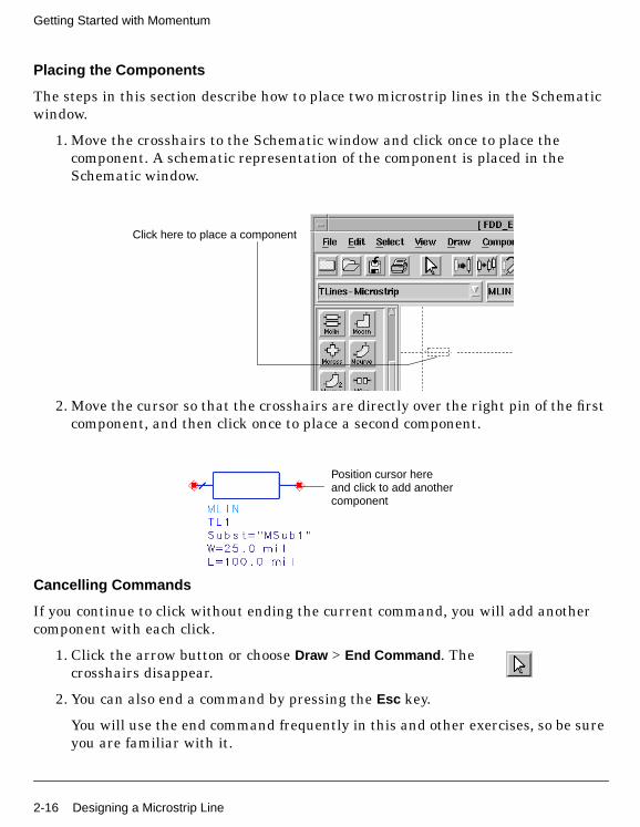
Placing the Components
The steps in this section describe how to place two microstrip lines in the Schematicwindow.
1. Move the crosshairs to the Schematic window and click once to place thecomponent. A schematic representation of the component is placed in theSchematic window.
2. Move the cursor so that the crosshairs are directly over the right pin of the firstcomponent, and then click once to place a second component.
Cancelling Commands
If you continue to click without ending the current command, you will add anothercomponent with each click.
1. Click the arrow button or choose Draw > End Command . Thecrosshairs disappear.
2. You can also end a command by pressing the Esc key.
You will use the end command frequently in this and other exercises, so be sureyou are familiar with it.
Click here to place a component
Position cursor hereand click to add anothercomponent

Designing a Microstrip Line 2-17
Editing Component Parameters
Below the schematic representation of each component are some of the editableparameters of the component. This section describes how to change the width of oneof the strips. The result is a microstrip step in width transmission line.
1. Click twice on the second component that you placed. The Libra Microstrip Linedialog box opens.
2. In the Select Parameter field, select the W (width) parameter. When the field tothe right shows the value of the width, change the value in this field to 35 mil.Click Apply.
3. Click OK to dismiss the dialog box.
Note If a parameter for a component is displayed in the Schematic window,you can also edit that parameter by clicking on the value and entering a newvalue.
4. Verify that the width of component on the left is set to 25 mil, and if needed,change the value of this parameter.
2-18 Designing a Microstrip Line
Getting Started with Momentum
Adding Ports to the Circuit
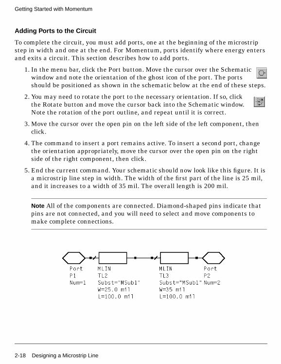
To complete the circuit, you must add ports, one at the beginning of the microstripstep in width and one at the end. For Momentum, ports identify where energy entersand exits a circuit. This section describes how to add ports.
1. In the menu bar, click the Port button. Move the cursor over the Schematicwindow and note the orientation of the ghost icon of the port. The portsshould be positioned as shown in the schematic below at the end of these steps.
2. You may need to rotate the port to the necessary orientation. If so, clickthe Rotate button and move the cursor back into the Schematic window.Note the rotation of the port outline, and repeat until it is correct.
3. Move the cursor over the open pin on the left side of the left component, thenclick.
4. The command to insert a port remains active. To insert a second port, changethe orientation appropriately, move the cursor over the open pin on the rightside of the right component, then click.
5. End the current command. Your schematic should now look like this figure. It isa microstrip line step in width. The width of the first part of the line is 25 mil,and it increases to a width of 35 mil. The overall length is 200 mil.
Note All of the components are connected. Diamond-shaped pins indicate thatpins are not connected, and you will need to select and move components tomake complete connections.

Designing a Microstrip Line 2-19
Saving the Design
It is good practice to save your work periodically. This section describes how to savethe schematic.
1. Choose File > Save. When the Save dialog box appears, enter the name of theproject, in this case, type step1 .
2. Click OK.
Generating the Layout
A powerful feature of Advanced Design System is the ability to convert a schematic toa layout automatically. Since Momentum requires a circuit be in Layout format, thisgives you the option of drawing your circuits either as schematics or as layouts. Notethat if you do choose to draw in a Schematic window, footprints of the components youuse must also be available in Layout. Components that are available in Layoutinclude transmission lines and lumped components with artwork.
This section describes how to covert the microstrip line step in width schematic thatyou just finished to a layout.
1. In the Schematic window, choose Layout > Generate/Update Layout . TheGenerate/Update Layout dialog box appears. It is not necessary to edit fields.
2. Click OK.
3. A Status of Layout Generation message appears indicating that the conversionis complete
4. Click OK.
5. A Layout window appears, showing a layout representation of the schematic.This window may be hidden by the Schematic window, so you may need to movesome windows to locate the Layout window.
6. From the Layout window, choose File > Save. Name the layout step1 . You nowhave a layout and a schematic as part of your project.

2-20 Designing a Microstrip Line
Getting Started with Momentum
Creating a Simple Substrate
A substrate is required as part of your planar circuit. The substrate describes themedia where the circuit exists. An example of a substrate is the substrate of amultilayer circuit board, which consists of:
• Layers of metal traces
• Layers of insulating material between the traces
• Ground planes
• Vias that connect traces on different layers
• The air that surrounds the circuit board
Momentum includes predefined substrates that you can add to a layout, or you canmake your own. Complete details about substrates, including where substrates aresaved, are in Chapter 3, Substrates.
The steps in this section describe how to define a substrate.
For the microstrip line step in width example, a substrate with the following layerswill be used:
• A ground plane
• A layer of insulation, such as Alumina
• A metal layer for the microstrip
• An air layer above the microstrip

Designing a Microstrip Line 2-21
1. From the Layout window, chose Momentum > Substrate > Create/Modify . TheCreate/Modify dialog box opens, showing the Substrate Layers options andparameters.
2. In the Substrate Layers field, select FreeSpace. Move to the Substrate LayerName field and change it to read Air. Leave all other parameters at theirdefault values and click Apply .
3. Keep the default layers Alumina and ///GND///, but highlight and Cut anyother layers that may be showing. Click Apply .
You currently see three of the four substrate layers that you need. The fourth(metal) layer can be found by clicking the Metallization Layers tab.

2-22 Designing a Microstrip Line
Getting Started with Momentum
The metal layer is automatically positioned between the layers of Alumina andair. The microstrip line is assumed to be on this layer.
4. Click OK to dismiss the dialog box.
5. To save the substrate with the project, choose Momentum > Substrate > Save As .Type step1 in the Selection field and click OK. The substrate step1.slm is savedin the project networks folder.
Some other information about saving substrates:
• A substrate definition is automatically saved with the design whenFile > Save is invoked from the Layout window
• The command Substrate > Save As enables you to save the substratedefinition inslm that can be saved anywhere and used with another design
• When a design is opened, the substrate definition that was saved with thedesign is automatically loaded

Designing a Microstrip Line 2-23
Precomputing the Substrate
In order to perform a simulation, Green’s functions that characterize the behavior ofthe substrate must be computed. Substrates that are supplied with Momentumalready include the computations. If you are:
• Reusing a substrate
• Have previously computed Green’s functions for the substrate
• Created a substrate that is identical to one that already exists
the attempt to perform the computations will be ignored, since the calculations aresaved in a database. In these cases, only if you extend the computation frequencyrange will additional calculations be performed.
The steps in this section describe how to precompute the substrate. Note that for thisexample, computations will not be performed. The substrate that was defined in theprevious example is, in fact, identical to one that is supplied with Momentum.
1. Choose Momentum > Substrate > Precompute Substrate Functions . Set theMinimum Frequency to 1 GHz and Maximum Frequency to 4 GHz. This is therange that the simulation will cover. You should check that computations existfor the entire range that you intend to simulate, but if you do not, an error willbe displayed if you need to run any computations.
2. Click OK.
• If a dialog box opens to ask if you want to compute the substrate, click Yes.Calculations will be performed.
• If a dialog box informs you that substrate calculations exist, click OK. Thecalculations will not be recomputed.
A status window also opens. You can leave this status window on the screen asyou proceed with this exercise.
This completes the process of defining a substrate.
Setting up Mesh Parameters
A mesh is required in order to perform a simulation. The simplest method forgenerating a mesh is to skip the Mesh menu entirely and let Momentumautomatically generate the mesh for your circuit, but you can choose to editparameters that control how the mesh is generated.

2-24 Designing a Microstrip Line
Getting Started with Momentum
A mesh is a grid-like pattern of triangles and rectangles that is applied the surfacesof a circuit. Using the mesh, the current within each triangular or rectangular area iscalculated, and any coupling effects in the circuit can also be calculated during thesimulation. From these calculations, S-parameters are then calculated for the circuit.
Complete details about mesh definitions and generation are in Chapter 6, Mesh.
The steps in this section describe how to set the frequency range for meshcomputations. All other options will remain at the default values.
1. In the Layout window, select Momentum > Mesh > Setup Controls . ACreate/Modify dialog box appears.
2. Set the value in the Mesh Frequency field to 4 GHz and click OK.
Precomputing the Mesh
If you want to view the mesh before simulation, you can precompute the mesh. Themesh will not be precomputed for this exercise.
This completes the process for generating a mesh.
All that is required is themesh frequency.Momentum uses defaultsto generate a valid mesh forthe circuit.
Designing a Microstrip Line 2-25
Performing the Simulation
The Momentum simulation process combines the Green’s functions that werecalculated for the substrate, plus the mesh information, and solves for currents in thecircuit. Using the current calculations, S-parameters are then calculated for thecircuit.
There are a variety of options to select to set up a simulation. Details are in Chapter7, Simulation. This section describes the minimal steps for running a simulation.
1. From the Layout window, choose Momentum > Simulation > Simulate Circuit . TheSimulation Control dialog box appears.
2. Set the Sweep Type to Linear and confirm that the following parameters areset:
• Start = 1 GHz
• Stop = 4 GHz
• Frequency Step = 1 GHz
By choosing this sweep type, a linear simulation will be performed over the 1-4GHz frequency range, selecting the frequency points to be simulated based onthe step size.

2-26 Designing a Microstrip Line
Getting Started with Momentum
3. Click Add to Frequency Plan List. The dialog box should resemble the figurehere.
4. Ensure that the field Open data display when simulation completes is enabled.
5. Click Simulate . The simulation will be performed. The simulation progress andits completion will be indicated in the Simulation Status window.
6. When the simulation is complete:
• The layout is overlaid with the mesh that was generated and used during thesimulation process.
• The S-parameter simulation results are automatically displayed on bothrectangular plots and Smith charts in a Data Display window. This isbecause the field Open data display when simulation is complete was enabledas a default in the simulation setup. Choose View > View All or click the View

Designing a Microstrip Filter 2-27
All button to view all of the plots, then zoom in on individual plots. Anexample of one S-parameter result is illustrated here.
This completes the first Momentum design exercise.
Designing a Microstrip FilterThis section is made up of an exercise that takes you through the process of designing a microstripcoupled-line filter. It is similar to the previous exercise, but uses fewer defaults and explores howto:
• Create a more complex substrate
• Specify port properties
• Use a box to simulate the filter within a metal enclosure
• Specify mesh parameters
Drawing the Circuit
This section is very similar to the drawing instructions in the previous exercise. Thecircuit is drawn as a schematic, then converted to a layout. If you need moreinformation on how to perform certain steps, refer to the previous exercise.
Opening a New Project
Like the previous exercise, start the filter design in a new project.
1. From the Main window, choose File > New Project .

2-28 Designing a Microstrip Filter
Getting Started with Momentum
2. Name the project filter.
3. Click Length Unit . Select millimeter to set the layout units for this circuit. ClickOK to set the units.
4. Click OK in the New Project dialog box to create the new project.
Adding Components to the Schematic
The steps in this section describe how to select microstrip filter components.
1. In the Schematic window, click the Palette List arrow. The Palette List dropsdown.
2. Scroll and select T-lines Microstrip from the Palette List.
3. In the component palette, locate and click Mcfil . This selects the LibraMicrostrip Coupled-Line Filter Section component.
4. Crosshairs and a ghost icon of the component appear as you move the cursorover the Schematic window. Position the cursor and click.
5. End the command either by clicking the Cancel Command button or by choosingDraw > End Command .
Editing the Component
This section describes how to edit several component parameters, such as the length and width,and also how to change the parameters that are displayed below the component.
1. To edit the component parameters, double click the component.
2. In the dialog box that appears, select one of the parameters listed below, andedit the value. Also, enable Display parameter on schematic so that theparameter will be displayed below the component in the Schematic window.Select another parameter, and continue to set the values for these parameters:
• W = line width = 0.25 mm
• S = spacing between lines = 0.044 mm
• L = line length = 1.8 mm
• W1 = width of the line that connects to pin 1 = 0.25 mm
• W2 = width of the line that connects to pin 2 = 0.25 mm
3. Click OK to accept the edits and dismiss the dialog box.

Designing a Microstrip Filter 2-29
Copying and Placing another Component
This section describes how to make a copy of the filter section and add it to theschematic.
1. From the Schematic window, choose Edit > Copy/Paste > Copy.
2. Click the filter section component that is on the schematic. A black outlineappears around it.
3. Move the crosshairs so that they are directly over the left connector of the firstcomponent and click.
4. End the current command.
Adding Ports
Ports are required on a circuit. If you forget to add ports to the schematic, you canalways add them later after the schematic is converted to a layout. In this exercise,ports will be added to the layout.
With Momentum, you can define additional characteristics to a port. This also will beperformed later in this exercise.
Your schematic should now look like the figure here. Be sure that all components areconnected correctly.

2-30 Designing a Microstrip Filter
Getting Started with Momentum
Saving the Design
It is good practice to save your work periodically.
1. Choose File > Save.
2. Enter filter as the file name.
3. Click OK.
Generating the Layout
This section describes how to covert the microstrip coupled-line filter schematic thatyou just finished to a layout.
1. From the Schematic window, choose Layout > Generate/Update Layout . TheGenerate/Update Layout dialog box and a Layout window appear.
2. From the Layout window, choose Options > Preferences . Click the Layout Unitstab and set the Resolution to 0.001. Click OK.
3. In the Generate/Update Layout dialog box, enter -1.8 in the X field and 0.294 inthe Y field. This step identifies the placement of P1 on the layout. This step isusually optional, but specifying the location will be helpful later when the box isadded to enclose the filter. Click OK.
4. A window displaying the results of the conversion is displayed. Click OK.
A layout representation of the schematic appears in the Layout window. It shouldresemble the figure here.
5. From the layout window, choose File > Save. Name the layout filter . You nowhave a layout and a schematic as part of your project.

Designing a Microstrip Filter 2-31
Defining a Substrate
This circuit uses a relatively simple substrate. In this exercise, the thickness of someof the layers is modified. A more important task is that ground planes are added tothe top and bottom of the substrate. These ground planes form the top and bottom ofthe metal box in which the filter will be enclosed. The substrate will have thefollowing layers:
• A ground plane representing the top of the box
• A layer of air
• The microstrip filter traces
• A layer of alumina
• A ground plane representing the bottom of the box.
1. From the Layout window, chose Momentum > Substrate > Create/Modify .
2. Select the top layer in the Substrate Layers field. In the Boundary list, selectClosed. The top ground plane is added to the substrate.
3. In the Substrate Layers list, select Free_Space. Change the Thickness to 2846um . This sets the layer of air to an appropriate thickness.

2-32 Designing a Microstrip Filter
Getting Started with Momentum
4. In the Substrate Layers list, select Alumina. Change the Thickness to 254 um .
5. Keep the bottom ground plane, but select and Cut any other layers that mayappear in the substrate.
6. Click Apply.
Note The top and bottom of the box enclosure are defined with groundplanes,the sides of the enclosure will be defined later in this exercise.
You currently see four of the five substrate layers that you need. The metallayer for the microstrip filter can be found by clicking the Metallization Layerstab.
In this instance, the metal layer is automatically positioned between theAlumina and air.
Note the following points about this layer:
• Metal layers are identified by a dashed line.
metal layer

Designing a Microstrip Filter 2-33
• The word cond identifies the layout layer that is mapped to this position.Refer to the Layout window, and you will see that the microstrip circuit wasautomatically applied to the layout layer named cond during the translationprocess.
• The word strip defines the layer such that the microstrips are metal andwhat surrounds the microstrips on that layer is air or dielectric. Otherchoices are slot and via. These are described in the exercise in the nextchapter.
7. Choose Momentum > Substrate > Save As . Use the file name filter and click OK.The substrate file filter.slm is saved as part of the project.
8. Choose Momentum > Substrate > Precompute Substrate Functions . Set MinimumFrequency to 1 GHz and Maximum Frequency to 40 GHz. Click OK. If a dialogbox appears and asks if you want to compute the substrate, click Yes.
There are instances when the computations will not be performed. This wasdiscussed in the previous exercise. If they are performed, a window opens thatindicates the status of the computations and when they are complete.
You can choose Momentum > Substrate > View Substrate Summary at any timeand see a summary of the substrate calculations that have been completed.
Adding Ports to the Layout
In Momentum, you can define the ports in your circuit to be one of several types.Depending on the type you choose, the ports will be characterized in different ways.This can impact the result of a simulation, because the simulation can take thesecharacteristics into account. With different port types, you can select one that bestmatches the intended application of your layout.
More detailed information about the various port types can be found in Chapter 4,Ports.
Ports are defined in a two-step process. First, ports are added to a circuit when thecircuit is drawn. Then, in Momentum, you specify the port type in order to tailor theport to your circuit. Note that you can add the port components at any time as youdraw the circuit, but before a port type can be specified, a substrate must be definedfor the circuit.
This section describes how to add ports to a layout and how to specify a port type forthem.

2-34 Designing a Microstrip Filter
Getting Started with Momentum
1. From the Layout window, click the port icon. A Port dialog box appears. Ifnecessary, set layer = cond . The ports must be on the same layout layer as themicrostrip filter. Click OK.
2. Move the cursor over the open port on the left side of the layout and click. Movethe cursor over the open port on the right side of the layout and click. End thecommand. The layout should resemble the figure here.
3. From the Layout window, choose Momentum > Port Editor . The Port PropertiesEditor dialog box.
4. If necessary, drag the dialog box away from the Layout window so that bothports are visible. Click the connector P1.

Designing a Microstrip Filter 2-35
5. The Port Properties dialog box will change so that you can select a port type tobe applied to P1.
6. Select Internal from the Port Type drop down list and click Apply .
7. Click the connector P2. Select Internal from the Port Type drop down list. ClickOK to accept the port type and dismiss the dialog box.
The internal port type is selected because it can be applied to the interior of acircuit. While normally this placement of the ports on the filter would not beconsidered internal, they are in this case because the filter is enclosed withinthe box. More information on this and other port types is in Chapter 4, Ports.
Finishing the Box around the Filter
Boxes and waveguide enclosures are useful because they introduce horizontalboundaries to the design. Adding a box enables you to look at box resonance, whichcan have a significant effect on S-parameters in a small band centered around the boxresonance frequency. More information about boxes, waveguides, and their uses arein Chapter 5, Boxes and Waveguides.

2-36 Designing a Microstrip Filter
Getting Started with Momentum
Recall that when you defined the substrate, you defined ground planes as the top andbottom of the metal box that will enclose the filter. This section describes how tospecify the dimensions and location of the sidewalls of the box.
1. From the Layout window, choose Momentum > Box & Waveguide > Add Box .
2. You will enter specific x, y coordinates for the left and right sides of the box.Choose Draw > Coordinate Entry . Type -4.5, -4.5 in the X,Y fields of theCoordinate Entry dialog box and click Apply .
3. Type +4.5, +4.5 in the X,Y fields of the Coordinate Entry dialog box and clickApply . The box appears as shown below (you may need to click View All to see thebox). Click Cancel to close the dialog box.
Generating a Mesh
This section describes how to specify additional mesh parameters.
1. From the Layout window, choose Momentum > Mesh > Setup Controls .
2. Set the following options and values:
• Mesh Frequency = 40.0 GHz. You should set the mesh frequency to thehighest frequency to be simulated.

Designing a Microstrip Filter 2-37
• Number of Cells per Wavelength = 20. This will be used to determine thedensity of the mesh. A mesh needs to be made up of small cells, but a meshthat is too dense over the entire circuit slows a simulation without addingmuch accuracy to results.
• Edge Mesh is enabled, and Edge Width = 0.05 mm. The edge mesh adds arelatively dense mesh along the edges of objects. Since most current flowsalong the edges of objects, using a denser mesh only on the edges can improvethe speed and accuracy of a simulation.
Leave the other settings as they appear.
3. When these selections are completed, click OK.
4. Choose Momentum > Mesh > Precompute Mesh . The mesh will be computed anddisplayed on the layout, like the figure here. If you have trouble seeing themesh, choose Options > Layers and reset the color and pattern values for thecond layer.
5. Save your work by choosing File > Save from both the Layout window and theSchematic window. Use the file name filter for both of them; Advanced DesignSystem can distinguish the layout from the schematic and will not overwriteone with the other.
Performing the Simulation
This section describes how to set up and run the simulation. In this exercise, theadaptive sweep type is used in the simulation process. This the preferred sweep type,because it used a fast, highly accurate method of comparing simulated data points toa rational fitting model. Unlike the linear sweep type, where simulated data pointsare chosen in a linear fashion based on step size, adaptive sweep type data points are

2-38 Designing a Microstrip Filter
Getting Started with Momentum
chosen based on where the most variance seen. Wherever S-parameters vary fromthe rational fitting model the most, more samples are taken.
1. From the Layout window, choose Momentum > Simulation > Simulate Circuit .
2. Select the Adaptive Sweep Type and set these parameters to the followingvalues:
• Start = 1 GHz
• Stop = 40 GHz
• Sample Points Limit = 50
3. Click Add to Frequency Plan List.
4. Make sure that Open data display when simulation completes is enabled TheS-parameters will automatically be plotted and displayed at the end of thesimulation.
5. Click Simulate . The simulation will be performed and its progress andcompletion will be indicated in the status window.
6. Click Momentum > Simulation > View Summary and saved simulation details willbe displayed. You can print the report if you wish.

Designing a Coplanar Waveguide Bend 2-39
Viewing Simulation Results
The S-parameter simulation results are automatically displayed on both rectangularplots and Smith charts in a Data Display window. An example of S12 plotted on arectangular plot is shown here.
Designing a Coplanar Waveguide BendThis exercise, like the previous exercises, takes you through all of the steps that arenecessary when designing with Momentum: creating a layout, defining a substrate,adding ports to the circuit, defining a mesh, simulating, and viewing results. Unlikethe previous exercises, this one explores the following design topics:
• Creating a layout that is drawn on more than one layer
• Using vias as connections between layers
• Specifying new port types
• Working with new mesh parameters

2-40 Designing a Coplanar Waveguide Bend
Getting Started with Momentum
This circuit drawn in this exercise is a coplanar waveguide bend. A coplanarwaveguide is, generally, slots filled with a dielectric or air, surrounded by metal, asshown in the figure here.
There are two basic methods for constructing coplanar waveguides in Layout, one isused in this exercise, the other is discussed in Chapter 5, Boxes and Waveguides.
Creating the Layout
In this example, the circuit is created entirely within the Layout window, and aschematic representation is not used. Be sure to save your work periodically.
The layout consists:
• Coplanar waveguide slots
• Bridges that span the two slots
• Vias that vertically connect the bridges to the slots
The slots will be drawn on one layer, the bridges will be drawn on a second layer, andthe vias on a third layer. This will be important for when these layers are mapped tothe substrate. An illustration of the circuit is shown on the left, the layout is on theright.
slots
metal ground plane
slots
bridge
bridgevias

Designing a Coplanar Waveguide Bend 2-41
1. From the Main window, choose File > New Project . Name the project cpw_bend .Click Length Unit , and set the units to millimeter . Click OK.
2. Set your preferences so that a Layout window will open instead of a Schematicwindow. From the Main window, choose Options > Preferences and enable CreateInitial Layout Window. Disable Create Initial Schematic Window.
3. Click OK in the open dialog boxes.
4. From the Layout window, choose Options > Preferences . Scroll to the LayoutUnits tab. Set the layout units to um and the resolution to 0.001. Click OK.
5. There is a difference between the length units that you chose when you createdthe new project, and the units that you just set. The units chosen when youcreated the project set the units of the layout window in which you are working.The units chosen through Options > Preferences sets the units for objects thatare drawn in the Layout window.
6. You will rename the layout layers that are used for drawing the slots, bridges,and vias of the coplanar waveguide bend. Using more descriptive names canhelp identify which layer that each part of the circuit is drawn on. ChooseOptions > Layers . From the Layers list, select cond . In the Name and LayerBinding List fields, enter slot . Click Update (located just below the Layers list).Select cond2 . In the Name and Layer Binding List fields, enter bridge . ClickUpdate . Select hole . In the Name field only, enter via and click Update . Click OK.
Drawing the Waveguide Slots
The section describes how to draw the coplanar waveguide slots.
1. Verify that slot is the current layer. The slots will be drawn on this layer. Thename of the current layer is displayed in the tool bar and at the bottom of theLayout window. If slot is not displayed, select it from the list.
select a layer
current layer and its color
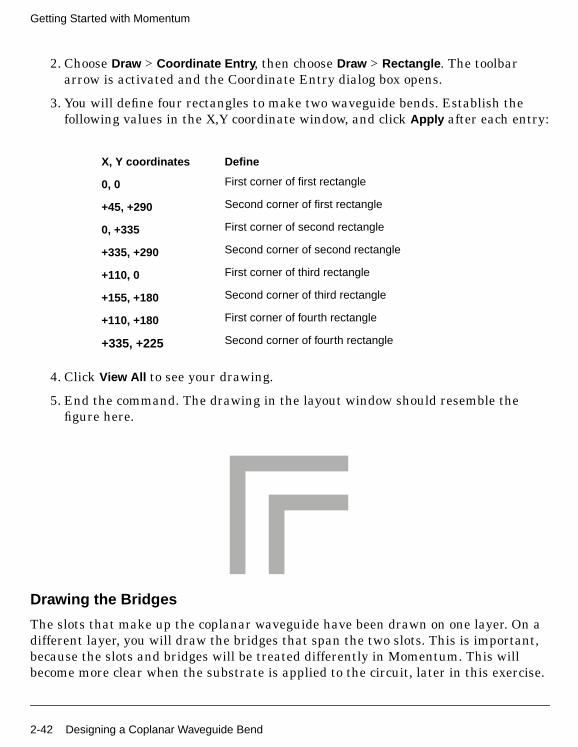
2-42 Designing a Coplanar Waveguide Bend
Getting Started with Momentum
2. Choose Draw > Coordinate Entry , then choose Draw > Rectangle . The toolbararrow is activated and the Coordinate Entry dialog box opens.
3. You will define four rectangles to make two waveguide bends. Establish thefollowing values in the X,Y coordinate window, and click Apply after each entry:
4. Click View All to see your drawing.
5. End the command. The drawing in the layout window should resemble thefigure here.
Drawing the Bridges
The slots that make up the coplanar waveguide have been drawn on one layer. On adifferent layer, you will draw the bridges that span the two slots. This is important,because the slots and bridges will be treated differently in Momentum. This willbecome more clear when the substrate is applied to the circuit, later in this exercise.
X, Y coordinates Define
0, 0 First corner of first rectangle
+45, +290 Second corner of first rectangle
0, +335 First corner of second rectangle
+335, +290 Second corner of second rectangle
+110, 0 First corner of third rectangle
+155, +180 Second corner of third rectangle
+110, +180 First corner of fourth rectangle
+335, +225 Second corner of fourth rectangle

Designing a Coplanar Waveguide Bend 2-43
1. From the layer list on the toolbar, select the layer bridge and click OK.
Note The slot layer is still visible. You will not do so here, but it can be madeinvisible if you go to the Layout window and choose Options > Layers , select theslot layer, and turn Visible off.
2. Choose Draw > Rectangle .
3. You will define two rectangles that make the bridges. Establish the followingvalues in the X,Y coordinate window, and click Apply after each entry:
4. End the current command. The drawing in the Layout window should now looklike the figure here.
Drawing a Via
The vias must be drawn on a third layer. This is necessary for when the vias aremapped to the substrate, later in this exercise.
X, Y coordinates Define
0, +170 First corner of first bridge
+155, +180 Second corner of first bridge
+155, +180 First corner of second bridge
+165, +335 Second corner of second bridge

2-44 Designing a Coplanar Waveguide Bend
Getting Started with Momentum
The position and size of a via is very important. The various snap modes in Layoutcan aid in drawing vias, as shown in this part of the exercise. More information onhow to draw vias and other drawing tips are in Chapter B, Drawing Tips.
1. From the layout layer list on the toolbar, select via.
2. Choose Options > Preferences . Scroll to and select Grid/Snap . Under Active SnapModes, enable Vertex and clear Grid . Click OK.
By using the vertex snap mode, the vias that you draw will snap to the vertex ofa nearby object (a bridge) and not to a grid point. This ensures that the vias willbe positioned precisely on the edges of the rectangles.
3. Choose Draw > Polyline . Referring to the points identified on the drawing below,create the line segments shown by performing these steps:
• Click once on A1 and click twice on A2.
• Click once on B1 and click twice on B2.
• Click once on C1, click once on C2, and click twice on C3. Then click thetoolbar arrow. The drawing in the Layout window should now appear asshown below.
A1
A2
B1 B2
C1C2
C3
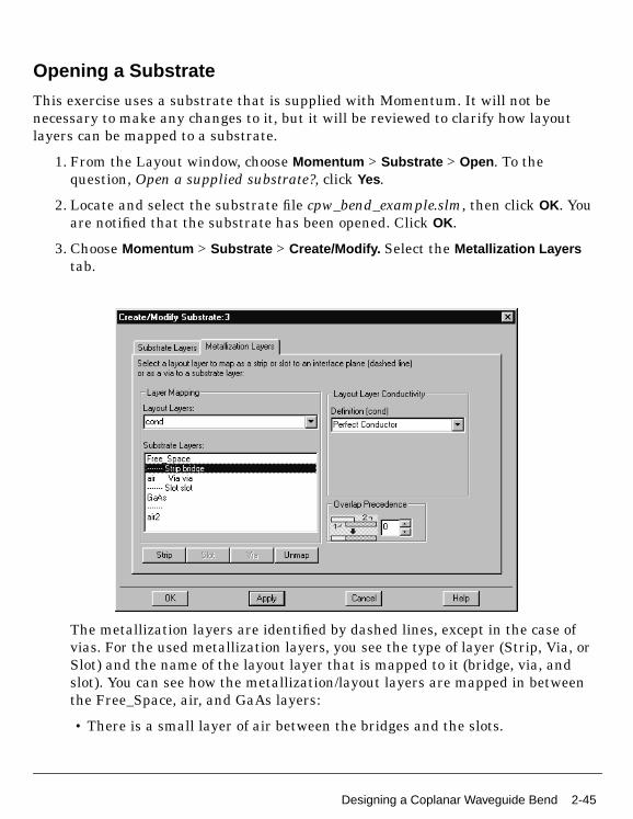
Designing a Coplanar Waveguide Bend 2-45
Opening a Substrate
This exercise uses a substrate that is supplied with Momentum. It will not benecessary to make any changes to it, but it will be reviewed to clarify how layoutlayers can be mapped to a substrate.
1. From the Layout window, choose Momentum > Substrate > Open . To thequestion, Open a supplied substrate?, click Yes.
2. Locate and select the substrate file cpw_bend_example.slm, then click OK. Youare notified that the substrate has been opened. Click OK.
3. Choose Momentum > Substrate > Create/Modify. Select the Metallization Layerstab.
The metallization layers are identified by dashed lines, except in the case ofvias. For the used metallization layers, you see the type of layer (Strip, Via, orSlot) and the name of the layout layer that is mapped to it (bridge, via, andslot). You can see how the metallization/layout layers are mapped in betweenthe Free_Space, air, and GaAs layers:
• There is a small layer of air between the bridges and the slots.

2-46 Designing a Coplanar Waveguide Bend
Getting Started with Momentum
• The vias are mapped the directly to the air substrate layer. The vias,although they are drawn as lines, are extruded by Momentum and effectivelycut vertically through this layer of air, connecting the edges of the slots andthe bridges.
• All three types of metallization layers, strip, slot, and via, are used here. Astrip defines the layer such that the bridges are metal and what surroundsthe microstrips on that layer is air. A slot is the opposite of a strip: the layoutlayer would be treated as a ground plane, and the bends that you have drawnare treated as open areas in the ground plane. Vias represent verticalsections that cut through other layers vertically.
Adding Ports
This section describes how to add ports to the layout and how to apply the coplanarport type to them.
Coplanar is one of the several port types that are available in Momentum. It isdesigned specifically for coplanar waveguide circuits, where an electric field is likelyto build up between two ports. Each of the two ports is excited with the same absoluteelectrical field, but with opposite polarity. The currents are equal but in opposite indirection. For more information, refer to Chapter 4, Ports.
1. The ports must be added to the waveguide slots and so they must be drawn onthe same layer as the slots. From the Layout Layers list box, select slot .
2. The ports must also be positioned in the center of each slot edge. To helpposition the ports, set the following snap modes:
• Enable Options > Midpoint Snap
• Enable Options > Edge Snap
• Disable Options > Vertex Snap and other enabled snap modes (but make surethat Options > Enable Snap remains enabled)
3. Click the Port icon. The Port dialog box appears.
4. Verify that layer=cond is displayed in the Select Parameter field. If it is not, setlayer to cond . Verify that Num=1 . If it is not, select Num and set it to 1. Click OK.
5. Note the ghost image of the port. If it appears very large, or if it cannot be seen,cancel the command. Depending on your system defaults, you may need tochange the value of the Port/Ground Size (Options > Preferences > Placement )

Designing a Coplanar Waveguide Bend 2-47
and the value of the Font Definition Size (Options > Preferences > ComponentText) before your ports and labels will be an appropriate size for this layout.
6. When you are ready to add ports, apply them in the order and direction asshown here, then end the port command.
7. From the Layout window, chose Momentum > Port Editor . The Port PropertiesEditor dialog box appears. You may need to drag the box away from the layoutin order to have access to the ports on the layout.
8. In the Layout window, click P1. In the Port Editor, select Coplanar from the PortType list. Set the Polarity to Normal . Do not change any other values. ClickApply .
9. Click P2. Select Coplanar and set the Polarity to Reversed . Type 1 in the fieldAssociate with port number. Click Apply .
10. Click P3. Select Coplanar and set Polarity to Reversed . Click Apply .
11. Click P4. Select Coplanar and set Polarity to Normal . Type 3 in the fieldAssociate with port number. Click Apply .
12. Click OK.

2-48 Designing a Coplanar Waveguide Bend
Getting Started with Momentum
Generating the Mesh
This section describes how to use additional mesh parameters. Because this circuit ison multiple layers, it is possible to set mesh parameters for each layer. Thus, you canset a relatively dense mesh on a specific layer. In this example, you will apply an edgemesh to the slot and via layers, but you will not use an edge mesh on the bridge layer.
1. From the Layout window, choose Momentum > Mesh > Setup Controls .
2. Set the following Global parameters:
• Mesh Frequency = 40 GHz
• Number of Cells per Wavelength = 100
• Enable Edge Mesh
Global parameters will be applied to all layers, unless other values are specifiedfrom the Layer tab.
3. Select the Layer tab.
4. In the Layout Layers list, select bridge . Set the Number of Cells per Wavelengthto 100 and disable Edge Mesh. These mesh parameters will be applied to theobjects drawn on the bridge layer only.
5. Click OK.

Designing a Coplanar Waveguide Bend 2-49
6. Select Momentum > Mesh > Precompute Mesh . Click OK to start thecomputations. The mesh will be computed and displayed on the layout, asshown here. Zoom in for a closer look at the mesh.
7. Zoom in on the ports. You can see that additional arrows have been added toeach port. The new arrow indicate the direction of the voltage over the slot.
Performing a Simulation
1. From the Layout window, choose Momentum > Simulation > Simulate Circuit .
2. From the Sweep Type list, select Adaptive and set these parameters:
• Start = 1 GHz
• Stop = 40 GHz
• Sample Points Limit = 50
3. Click Add to Frequency Plan List.
4. Make sure that Open data display when simulation completes is enabled.
5. Click Simulate .

2-50 Designing a Coplanar Waveguide Bend
Getting Started with Momentum
Viewing Simulation Results
The figure shows some of the automatically plotted simulation results.
To save your work, choose Yes to All when you are asked to save your work when youclose the project.
This concludes the third exercise.

3-1
Chapter 3: SubstratesA substrate definition describes the media where a circuit exists. An example is thesubstrate of a multilayer circuit board which consists of layers of metal traces,insulating material, ground planes, vias that connect traces, and the air thatsurrounds the board. A substrate definition enables you to specify properties such asthe number of layers in the substrate, the dielectric constant, and the height of eachlayer for your circuit.
A substrate definition is made up of substrate layers and metallization layers.Substrate layers define the dielectric media, ground planes, covers, air or otherlayered material. Metallization layers are the conductive layers in between thesubstrate layers, and they are used in conjunction with the layout layers. By mappinglayout layers to metallization layers, you can position the layout layers that yourcircuit is drawn on within the substrate. An example of a substrate is shown below. Itcontains four substrate layers and two microstrips with a via.
Substrate definitions can be saved and used with other circuits. A variety ofpredefined substrates are included with Advanced Design System, which can be used“as is” or modified to your design specifications.
Free_Spacetop layer = open (air)
Layout layer(strip in betweenAlumina_0 andFree_Space)
Substrate Layers:
Alumina_0(dielectric)
Alumina(dielectric)
////// GND //////Layout layer (via throughAlumina_0)
Layout layer(strip in betweenAlumina andAlumina_0)

3-2 Selecting a Predefined Substrate
Substrates
The steps for defining a substrate include:
• Defining the substrate layers
• Mapping the layout layers to metallization layers
• Specifying metallization layer conductivity
• Solving the substrate
Details on how to work with existing substrate definitions and create new ones follow.
Selecting a Predefined SubstrateMomentum includes a number of predefined substrate definitions, so it may not benecessary to create a substrate from scratch. A predefined substrate may be suitableso that it can be used it as is or modified to suit your design. Substrate files end withthe extension .slm.
To open a predefined substrate:
1. In the layout window, select Momentum > Substrate > Open.
2. If you want to open a supplied substrate, click Yes. A list of supplied substratefiles appears.
If you want to open a substrate that has been saved as part of the project, clickNo. A list of substrate files that are saved as part of the project appear.
For more information on locating substrate files, refer to “Identifying WhereSubstrates are Saved” on page 3-4.
3. Select the substrate file, then click OK.
To edit the substrate, refer to “Defining Substrate Layers” on page 3-5.

Reading a Substrate Definition from a Schematic 3-3
Reading a Substrate Definition from a SchematicChoose Momentum > Substrate > Update From Schematic to update a substrateunder the following conditions:
• You have used a substrate component on a schematic, such as MSUB or SSUB
• You have already generated a layout from the schematic using Layout >Generate/Update Layout
• You then change the substrate definition on the schematic, and need to transferit to the layout
In order to retrieve the new substrate information, you must use Momentum >Substrate > Update From Schematic. Using Layout > Generate/Update Layout willnot transfer the new substrate information to the layout.
To update a substrate definition from a schematic:
1. Choose Momentum > Substrate > Update From Schematic . The substrate on thecorrect schematic is read and the new information is entered in the Momentumsubstrate definition.
Saving a SubstrateA substrate definition can be saved to a file. This enables you to store the definitionoutside of the current project, making it easier to use the substrate definition in otherdesigns. To save a substrate:
1. Choose Momentum > Substrate > Save As .
2. Type a name for the file and click OK. Substrate files end with the extension.slm.
To save a named file, choose Momentum > Substrate > Save . The substrate informationis saved in a file called <substrate_name>.slm under /networks in the current projectdirectory.

3-4 Creating/Modifying a Substrate
Substrates
Identifying Where Substrates are Saved
Substrates are saved in one of two locations:
• In the directory containing supplied substrates, which is$HPEESOF_DIR/momentum/lib/substrates. You should not use this locationfor substrates that you have created or modified.
• The location that the environment variable $HOME points to. If this variable isnot defined, substrates are saved in the current project folder.
Creating/Modifying a SubstrateTo create or modify (edit) a substrate definition, use the procedures in “DefiningSubstrate Layers” on page 3-5 and “Defining Metallization Layers” on page 3-12.
Changing SubstratesIf you no longer want to use the substrate definition assigned to your design, or tochoose a different substrate use the procedure in “Selecting a Predefined Substrate”on page 3-2.
Deleting a SubstrateThis command erases the substrate file that you select. If the substrate has beenprecomputed, the calculations remain in the database.
To delete a file:
1. Choose Momentum > Substrate > Delete .
2. Select the name of the file that you want to delete.
3. Click OK.

Defining Substrate Layers 3-5
Defining Substrate LayersYou can define a substrate from scratch or edit an existing one. A substrate musthave, at the minimum, a top plane and a bottom plane.
Note Do not use substrate components that might appear on layout componentpalettes. You must use the dialog box under Momentum > Substrate > Create/Modifyto create or edit substrate definitions.
To define substrate layers:
1. Choose Momentum > Substrate > Create/Modify .
2. If this is a new definition, three default layers appear in the Substrate LayersField:
• Free_space (top plane)
• Alumina (dielectric)
• GND (bottom plane)
These layers represent a basic substrate definition that includes the three typesof substrate layers in Momentum.
• Free_Space represents the top plane of the substrate. In this definition, it isdefined as an open boundary.
• Alumina represents a dielectric layer of finite thickness. These layers arealso referred to as interface layers.
• GND represents the bottom plane of the substrate. GND defines a closedboundary. Closed boundaries define ground planes or other closedboundaries, such as the lid or bottom of an enclosure.
For an existing substrate definition, you may see more layers with differentnames, but they will all be one of these three basic types of layer, and thesubstrate will have a top and bottom plane. A substrate definition must have atop plane and a bottom plane, and these planes can be defined either as openboundaries or closed boundaries.
3. Select the layer of interest.

3-6 Defining Substrate Layers
Substrates
4. To create a substrate, you will edit these layers, rename them, and add to themas desired. For more information on how to perform these tasks, refer to thesections below.
5. When you are finished defining the substrate, click OK to dismiss the dialog box.
Defining an Open Boundary
An open boundary represents a layer of infinite thickness, such as air. An openboundary can be used to define other gases or infinitely-thick materials by editing therelative permeability and permittivity values of the boundary.
To define an open boundary:
1. Select the Free_Space layer or another open boundary layer.
2. Select Open from the Boundary list.
3. From the Permittivity (Er) listbox, select a format for the relative permittivityof the boundary. You can enter the components of relative permittivity as:
• Real and imaginary
• Real and loss tangent
• Real and conductivity, conductivity in Siemens/meter
The real portion of the relative permittivity, , is a dimensionless quantity andis identical to the material’s relative dielectric constant, . For more
information on this parameter, refer to “Dielectric Permittivity” on page 3-21.
To represent a dielectric that dissipates the power of a high-frequency electricfield, enter the dielectric loss tangent, , of the material in the LossTangent field. The smaller the loss tangent, the less lossy the material. Formore information on this parameter, refer to “Dielectric Loss Tangent” onpage 3-22.
Enter the components of the relative permittivity in the fields below the listbox.
ε′εr
ε″ ε′⁄

Defining Substrate Layers 3-7
4. From the Permeability (Mu) listbox, select a format for the relativepermeability of the boundary. You can enter the components of relativepermeability as:
• Real and imaginary
• Real and loss tangent
The real portion of the relative permeability, , is a dimensionless quantityand is identical to the material’s relative permeability constant. For moreinformation on this parameter refer to “Dielectric Relative Permeability” onpage 3-23.
To represent a dielectric that dissipates the power of a high-frequency magneticfield, enter the magnetic loss tangent, , of the material in thePermeability Loss Tangent field. The smaller the loss tangent, the less lossy thematerial. For more information on this parameter, refer to “Dielectric MagneticLoss Tangent” on page 3-24.
Enter the components of the relative permeability in the fields below thelistbox.
5. Click Apply to accept the open boundary definition.
Tip You can create a ground plane from a open boundary layer by selecting the layerand choosing Close from the Boundary list.
Defining an Interface Layer
Interface layers have finite thickness, and they can be characterized using relativepermittivity and permeability values. The thickness of a layer can be an arbitraryvalue, with these considerations:
• Thin substrates are substrates less than one micron in thickness, and theyrequire special meshing considerations. Substrates less than 0.1 micron shouldbe avoided.
• Thick substrates should be less than 0.5 wavelength in thickness. Therecommendation for thick substrates is based upon typical design values. Forexample, a 10 mil substrate with a cover height (air) of 300 mils would beacceptable for frequencies up to 20 GHz, which is 0.5 wavelength.
µ′
µ″ µ′⁄

3-8 Defining Substrate Layers
Substrates
To edit an interface layer:
1. Select the Alumina layer or other interface layer of interest.
2. Enter the thickness of the layer in the Thickness field and select theappropriate units in the adjacent listbox.
3. From the Permittivity (Er) listbox, select a format for the relative permittivityof the boundary. You can enter the components of relative permittivity as:
• Real and imaginary
• Real and loss tangent
• Real and conductivity, conductivity in Siemens/meter
The real portion of the relative permittivity, , is a dimensionless quantity andis identical to the material’s relative dielectric constant, . For more
information on this parameter, refer to “Dielectric Permittivity” on page 3-21.
To represent a dielectric that dissipates the power of a high-frequency electricfield, enter the dielectric loss tangent, , of the material in the LossTangent field. The smaller the loss tangent, the less lossy the material. Formore information on this parameter, refer to “Dielectric Loss Tangent” onpage 3-22.
Enter the components of the relative permittivity in the fields below the listbox.
4. From the Permeability (Mu) listbox, select a format for the relativepermeability of the boundary. You can enter the components of relativepermeability as:
• Real and imaginary
• Real and loss tangent
The real portion of the relative permeability, , is a dimensionless quantity.For more information on this parameter refer to “Dielectric RelativePermeability” on page 3-23.
To represent a dielectric that dissipates the power of a high-frequency magneticfield, enter the magnetic loss tangent, , of the material in thePermeability Loss Tangent field. The smaller the loss tangent, the less lossy thematerial. For more information on this parameter, refer to “Dielectric MagneticLoss Tangent” on page 3-24.
ε′εr
ε″ ε′⁄
µ′
µ″ µ′⁄

Defining Substrate Layers 3-9
Enter the relative permeability components in the fields below the listbox.
5. Click Apply to accept the layer definition.
Defining a Closed Boundary Layer
A closed boundary represents a plane, such as a ground plane. It is a layer with zerothickness. It can be defined as a perfect conductor, or you can specify bulkconductivity or sheet impedance to characterize it as a lossy conductor.
To edit a ground plane:
1. Select the ///GND/// layer of interest.
2. Select Closed from the Boundary list.
3. From the Plane listbox, select a format for the ground plane. You can specify theground plane using these parameters:
• Perfect conductor
• Bulk conductivity in Siemens/meter
• Sheet impedance in Ohms/square
Conductivity is entered as a real number. Impedance is entered as the real andimaginary components of a complex value.
Enter the ground plane parameters in the field below the listbox.
4. Click Apply to accept the closed boundary definition.
Tip You can create an open boundary layer from a ground plane by selecting theground plane and choosing Open from the Boundary list.

3-10 Defining Substrate Layers
Substrates
Renaming a Layer
To rename a layer:
1. Select a substrate in the Substrate Layers list.
2. The name appears in the Substrate Layer Name field. Edit the name as desired.
3. Click Apply .
Note A ground plane is identified as ///GND/// and its name cannot be changed.
Deleting, Adding, and Moving Layers
To organize your substrate layers in the correct order, you can delete, add, and movelayers.
To delete a substrate layer:
1. Select a substrate in the Substrate Layers list.
2. Click Cut . The layer definition is deleted.
To add a substrate layer:
1. Select a substrate in the Substrate Layers list that has the same basic property(open boundary, closed boundary, or finite thickness) as the layer you areadding.
2. Click Add .
3. The new layer is highlighted. To rename the new layer, edit the Substrate LayerName field.
4. To move the layer, refer to the steps below.
To move a substrate layer:
1. Select the substrate that you want to move from the Substrate Layers list.
2. Click Cut .
3. Select the substrate that you want positioned below the substrate that you aremoving.
4. Click Paste .

Defining Substrate Layers 3-11
Defining Silicon Substrate Layers
The electrical behavior of Silicon material is usually specified using the dielectricconstant and a resistivity (or conductivity value).
For the dielectric constant, a value for of 11.8 or 11.9 is usually used.
Resistivity ( ) values are normally specified in ohm cm, and a typical value is 10.
In Momentum, you can specify the conductivity ( ) in S/m (inverse of the resistivity).
Foe more information, see “Dielectric Conductivity” on page 3-22.
Calculating Conductivity from Resistivity
Conductivity is simply the inverse of resistivity. Make certain that the units ofresistivity are ohms m before inverting.
Example:
1. = 10 ohm cm
2. = 10 ohm cm = 0.1 ohm m
3. = 1/rho = 10 S/m
Defining Conductivity
To define conductivity for silicon substrates:
1. Choose Momentum > Substrate > Create/Modify .
2. In the Create/Modify dialogue box, select RE, Conductivity under Permittivity(ER).
3. Specify the substrate dielectric constant and conductivity (S/m).
4. When you are finished, click OK to dismiss the dialog box.
ε′
ρ
σ
ρ
ρ
σ

3-12 Defining Metallization Layers
Substrates
Defining Metallization LayersMetallization layers enable you to:
• Define the position of layout layers in the substrate
• Specify which parts of the layer are conductive
• Define the conductivity of the layout layers
In order to identify which areas of a layout layer are conductive, a layer can bespecified as:
• Strip—The objects on the layout layer are conductive, the rest of the layer is not
• Slot—The inverse of a strip, the objects on the layout layer are not conductive,but the rest of the layer surrounding the objects is conductive. When simulated,Momentum considers the electric field distribution (the equivalent magneticcurrent flow) in the slot.
the hairpin filter objects are conductive andmapped to a strip metallization layer
Physical Slot
metal
Slot metallizationlayer in Momentum
metal

Defining Metallization Layers 3-13
• Via—The objects on the layout layer are conductive and cut vertically throughone or more substrate layers. For more information on how to draw and applyvias, refer to “Applying Vias” on page 3-29 and “Drawing Vias in Layout” onpage B-8.
Some examples of using strips and slots include:
• The patches of the Double_Patch antenna example. They are drawn on thelayout layer named top_met, and are conductive. This layer is mapped to ametallization layer that is defined as a strip.
• The slots of the Slot_dipole antenna example. The slots are drawn on the layoutlayer named slot. The slots are not conductive, but the area surrounding theslots is. This layer is mapped to a metallization layer that is defined as a slot.
Note that a layout can have many other layers that are not part of the actual circuit,such as text or error reporting layers. For the purposes of an Momentum simulation,they are ignored. If layout layers containing parts of the circuit are not mapped tometallization layers, they are ignored as well.
The steps for defining metallization layers are:
• Mapping a layout layer to a metallization layer
• Defining the conductivity of the layer
• Setting overlap precedence
Details for performing these steps are presented in the following sections.
bridge
via
strip
Examples of vias as sheets and cylinders
via
stripvia

3-14 Defining Metallization Layers
Substrates
Mapping a Layout Layer
Layout layers that contain any shapes or components that are part of the circuit mustbe mapped to metallization layers. If layout layers are not mapped to metallizationlayers, they will not be included in the simulation.
To map a layout layer:
1. Choose Momentum > Substrate > Create/Modify .
2. Click the Metallization Layers tab.
3. Select a layer from the Layout Layers list box. Note that the layout layerdefault cannot be mapped to a metallization layer, the first valid layer is cond.
4. To map the layer as a slot or strip, select from the Substrate Layers list adashed line to position the slot or strip in between two substrate layers, thenclick Strip or Slot .
If you make a mistake, click Unmap , then click the correct choice.
• A Strip defines the objects on the layout layer as conductive, the areasurrounding the objects is not.
• A Slot is the inverse of a strip, it defines the objects on the layout layer as notconductive, but the area of this layer surrounding the objects is conductive.When simulated, Momentum considers the electric field distribution (theequivalent magnetic current flow) in the slot.
5. To map the layer as a via, select the substrate layer that you want the via to cutthrough, then click Via.
If you want the via to cut through more than one layer, select the next layer,then click Via again.
• A Via defines the objects on the layout layer as conductive and they verticallycut through one or more substrate layers.
6. To define the conductivity characteristics of this layer, refer to “DefiningConductivity” on page 3-15.
7. If you have or suspect that you have overlapping layers, you need to set overlapprecedence. Refer to “Setting Overlap Precedence” on page 3-16.
8. Click the Apply button.

Defining Metallization Layers 3-15
Unmapping a Layer
If you want to change the location of a layer or remove one from the substratedefinition, use Unmap.
To unmap a layer:
1. Choose Momentum > Substrate > Create/Modify .
2. Click the Metallization Layers tab.
3. In the Substrate Layers list, select the substrate layer or the interface wherethe layout layer is mapped.
4. Click Unmap . This removes all layout layers assigned to this position.
5. To remap a layer, refer to the steps in “Mapping a Layout Layer” on page 3-14.
Defining Conductivity
You can define a layout layer as a conductor or a resistor. If the layout layer is definedas a strip or via, you define the conductivity of the strip or via. If the layout layer isdefined as a slot, you define the conductivity of the metal around the slot.
To define conductivity:
1. Choose Momentum > Substrate > Create/Modify .
2. Choose Metallization Layers.
3. Select a mapped layout layer from the Layout Layers list.
4. Select the conductivity definition from the Definition list:
• Perfect conductor
• Sigma, using real and conductivity values
• Sigma, using real and imaginary values
• Impedance
Perfect Conductor means the strip, via, or metal around the slot is a perfectconductor and is lossless. No further definition is required.
Sigma (Re, thickness) enables you to specify conductivity in terms of bulkconductivity and thickness. Enter bulk conductivity as a real value in theConductivity field, in Siemens/meter or Siemens/centimeter. Enter the metal

3-16 Defining Metallization Layers
Substrates
thickness in the Thickness field and select the appropriate units. These valueswill be used to calculate the dc and high frequency loss mechanisms whendetermining the equivalent surface impedance. For example, the bulkconductivity of gold is 41,000,410 Siemens per meter with any arbitrarythickness.
Sigma (Re, Im) specifies bulk conductivity as a complex number. Enter the realand imaginary component of the value in the Real and Imaginary fields,respectively, in Siemens/meter or Siemens/centimeter. The bulk conductivitywill be used to calculate the high frequency loss mechanisms, which are thenapplied to all frequencies when determining the equivalent surface impedance.The imaginary value is important for super-conductivity applications.
Impedance (Re, Im) specifies conductivity in terms of sheet impedance, inOhms/square. Enter the real and imaginary component of the value in the Realand Imaginary fields, respectively.
5. When you are finished with the definition, click Apply .
6. Repeat these steps for the remaining mapped layout layers.
7. When you are finished, click OK to dismiss the dialog box.
Setting Overlap Precedence
Overlap precedence specifies which layout layer has precedence over another if two ormore layout layers are assigned to the same metallization layer and objects on thelayers overlap. Precedence is used by the mesh maker so that objects on the layerwith the greatest precedence number are meshed and any overlap with objects onlayers with lesser numbers is logically subtracted from the circuit. If you do not setthe precedence, and there are overlapping objects, a mesh will automatically and

Defining Metallization Layers 3-17
arbitrarily be created, with no errors reported. Resistive layers generated fromschematics are automatically set to the highest precedence.
In some cases, you may be designing with an intentional overlap because ofmanufacturing layout guidelines. In this case, assign a precedence number to thelayout layers that overlap with precedence order in reverse numerical order (largestto smallest). The system will draw the boundary at the edge of the higher numberedlayer without returning an error.
Precedence affects only how the mesh is created, it does not affect or alter the layoutlayers in your design.
To specify overlap precedence:
1. Choose Momentum > Substrate > Create/Modify .
2. Choose Metallization Layers.
3. Select one of the overlapping layout layers in the list of Substrate Layers.
4. Assign its order of precedence in the Overlap Precedence field. Either type avalue directly into the field or use the arrow keys to select a value.
5. Click Apply .
6. Repeat these steps for the remaining overlapping layers.
7. When you are finished, click OK to dismiss the dialog box.
Overlap removed, geometry of object on top layer is altered
Precedence = 1 Precedence = 2
3-18 Precomputing the Substrate Function
Substrates
Precomputing the Substrate FunctionIn order to perform a simulation and to calculate a mesh, Green’s functionscharacterizing the behavior of the substrate must be computed:
• If you intend to precompute a mesh before you simulate, you must precomputethe substrate first. For more information on precomputing a mesh, refer to“Precomputing a Mesh” on page 6-11.
• If the Green’s functions are not computed before you start a simulation, theywill be calculated and then the simulation will run.
If you are using a substrate that is supplied with Advanced Design System, you donot need to precompute the substrate functions. If you have edited the substrate orcreated a new one, you must precompute the substrate function.
When the computations (Green’s functions) are complete, the data is stored in adatabase, and it will be used in the simulation of any design that uses this substrate.If the substrate has been precomputed before and there has been no changes to thesubstrate, it will not be recomputed unless the frequency range has been extended.The frequency range can be set when using the Momentum mode, but not inMomentum RF mode. In RF mode, the frequency range (start-stop) is not requested.Since the RF mode uses the quasi-static Green’s functions, they are calculated atquasi-static frequencies automatically chosen by the program. Substrate functionscalculated in Momentum mode are reusable in RF mode if they are calculated fromDC to some upper frequency.
For more information about the precomputation process, refer to Appendix A, Theoryof Operation.
To precompute the substrate function:
1. Choose Momentum > Substrate > Precompute .
2. To specify the frequency range of the computations, enter starting frequency inthe Minimum field and select the frequency units. Enter the stopping frequencyin the Maximum field and select the frequency units. (Not available in RFmode.)
Be sure that the frequency range includes all frequencies that you want tosimulate.
3. Click OK to start the computations.

Stopping Substrate Computations 3-19
Once the computations are completed, you do not need to perform this step againunless the substrate is edited.
Note Be aware that the greater the number of layout layers in the substrate, themore time required to perform the calculation.
Viewing Substrate Computation Status
After the substrate calculations are started, any messages regarding the calculationswill appear in the Momentum Status window. Messages usually refer to any errorsfound, and indicate when the calculations are complete.
If you close the status window and want to reopen it, from the Layout menu barchoose Window > Restore Status.
Stopping Substrate ComputationsTo stop the substrate calculations:
1. From the Momentum Status window, choose Simulation/Synthesis > StopSimulation .
The computations will stop and no information will be saved.
Viewing the Substrate SummaryIf the simulation is successful, you can view substrate, mesh, and solution statistics.Some of the information returned includes time to solve, the resources required, andcell information. An example of solution statistics is given next.

3-20 Reusing Substrate Calculations
Substrates
To view the summary, choose Momentum > Substrate > Summary.
====================================================================== --- STATUS SERVER MESSAGES ---======================================================================
Simulation / Synthesis Messages
Substrate to be computed from 9 GHz to 11 GHz!
Status / Summary
---------Momentum Simulation ------------------
Version: Momentum 4.0 (*) 150.100 Sep 25 2000Simulation mode: microwaveDesign: circular_polarization
Start compute substrate functions on Tue Oct 03 10:11:16 2000Computation 0.0% complete.Computation 2.6% complete.======================================================================
Reusing Substrate CalculationsSubstrate definitions and substrate computations can be reused for other designs, ifthe substrate database is accessible. If you are unsure about access to the database,consult your system administrator.
Before a calculation begins, several folders are searched to determine if a solution hasalready been generated. The folders searched, in order, are:
• The project networks folder
• The home directory or the site directory (made available by your systemadministrator)
• The folder containing the Momentum supplied substrates($HPEESOF_DIR/Momentum/lib)
If the Substrate Calculator finds the same substrate definition, regardless of thename, it uses the one it finds instead of recomputing the same information.

About Dielectric Parameters 3-21
About Dielectric ParametersThe sections below give additional detail about the following dielectric parameters:
• “Dielectric Permittivity” on page 3-21
• “Dielectric Loss Tangent” on page 3-22
• “Dielectric Conductivity” on page 3-22
• “Dielectric Relative Permeability” on page 3-23
• “Dielectric Magnetic Loss Tangent” on page 3-24
Dielectric Permittivity
The relative permittivity of all dielectrics is assumed to be complex:
which can also be expressed as:
where is the real portion of and is the dielectric loss tangent.
Examples of materials and their typical permittivity are shown in Table 3-1.
Note The values listed in the table are for illustrative purposes only; use valuesspecifically measured for the materials that you are using.
Table 3-1. Materials and Permittivity
MaterialRelativePermittivity
Alumina 9.8
Sapphire 9.3 - 11.7
Berrylia 6.0
Rutile 100.0
GaAs 12.9
ε ε' jε''+=
ε ε' 1( jε''ε'−−
+=
ε′ ε ε″ ε′⁄

3-22 About Dielectric Parameters
Substrates
Dielectric Loss Tangent
The dielectric loss tangent associated with a material is a function of frequency.Examples of dielectric loss tangents for 10 GHz fields are shown inTable 3-2.
Note These values are listed for illustrative purposes only. Use values specificallymeasured for the materials that you are using.
Dielectric Conductivity
For some materials (for example, Silicon), the substrate loss effects are betterdescribed using the combination ( , = conductivity) instead of ( , loss tangent).The complex dielectric constant is related to ( , conductivity) using the followingformula:
where:
= 2 frequency
= 8.85e-12 F/m (absolute dielectric constant free space)
Often, resistivity ( ) is specified instead of conductivity. The relationship betweenresistivity and conductivity is
Resistivety is usually specified in cm, conductivity is specified in S/m.
Table 3-2. Materials and Dielectric Loss Tangent
MaterialDielectricLoss Tangent
Alumina .0002
Glass .002
Berrylia .0001
Rutile .0004
GaAs .0016
ε′ σ ε′ε′
ε ε′ jσ( ) ωε0( )⁄( )–=
ω π
ε0
ρ
ρ 1 σ⁄=
Ω

About Dielectric Parameters 3-23
Example:
A typical value for resistivity of a Silicon material is
= 10 cm
which corresponds to a conductivity value of
= 10 S/m.
Dielectric Relative Permeability
The relative permeability of all dielectrics is assumed to be complex:
which can also be expressed as:
where is the real portion of and is the magnetic loss tangent.
ρ Ω
σ
µ µ' jµ''+=
µ µ' 1( jµ''µ'−−−
+=
µ′ µ µ″ µ′⁄

3-24 About Dielectric Parameters
Substrates
Examples of relative permeabilities are shown in Table 3-3.
Note The values listed above are for illustrative purposes only. Use valuesspecifically measured for the materials that you are using.
Dielectric Magnetic Loss Tangent
The magnetic loss tangent associated with a material is a function of frequency. Anexample of a material with a magnetic loss tangent is polyiron which, at 30 GHz, hasa loss tangent of 0.0208.
Table 3-3. Materials and Relative Permeability
MaterialRelativePermeability
Gold .99996
Air 1
Aluminum 1.00002
Nickel 250
Iron 4000

Substrate Definition Summary 3-25
Substrate Definition SummaryThe entire substrate definition includes:
• Vias, in the same manner that they are part of the fabrication process.
• Air bridges, including their height and their associated vias.
• Holes in ground planes, if they are part of a slot signal path (slot or coplanar),or if they are relief holes for vias passing through a ground plane are also partof the media.
• Dielectric layer properties (Er, Mu, and loss).
• Ground plane losses and cover properties (conductivity or impedance).
Not included as part of the media or substrate definition are metal loss of strip andvia layers. The numerical computation process, used by the substrate calculator, cantake as little as one minute for stripline circuits. It can take several minutes formicrostrip or even a few hours for an arbitrary multi-layered substrate with severalvias.
Every change to a substrate definition requires a complete re-computation. Thesystem checks for duplicate definitions, regardless of the name, and uses previouslycomputed data if it exists.
Substrate ExamplesUse the following examples to help you set up your own circuits:
• “Substrate for Radiating Antennas” on page 3-26
• “377 Ohm Terminations and Radiation Patterns” on page 3-26
• “Substrate for Designs with Air Bridges” on page 3-26

3-26 Substrate Examples
Substrates
Substrate for Radiating Antennas
To define a substrate for an antenna that radiates into air, you can set up thefollowing substrate definition:
Both layers are defined as open boundaries with the characteristics of air (forpermittivity and permeability, Real = 1, Loss Tangent = 0). The antenna design ispositioned on the metallization layer in between the two layers of air.
377 Ohm Terminations and Radiation Patterns
It is possible to define the top and bottom layers of a design with 377 ohmterminations, then calculate radiation patterns for these structures after simulation.For such applications, note the following considerations:
• The actual value of the termination may be between 376 and 378 ohms.
• When replacing top or bottom ground layer with a 377 ohm termination, a thicklayer of air in between the circuit and the 377 ohm termination is required inorder to get agreement (both for S-parameter results and radiation patterns)with the simulation results with infinite top or bottom layer. An air layer of10-20 substrate thicknesses is generally thick enough.
• There is a test on the impedance value prior to calculating the radiationpatterns. The impedance value must be in the interval (377 - 10) to (377 + 10)ohm.
Substrate for Designs with Air Bridges
In order to designing a substrate definition for a design that contains an air bridge,you need to first identify components of the air bridge and their placement on layoutlayers. Refer to the illustration that follows.
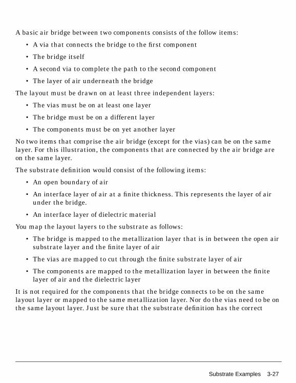
Substrate Examples 3-27
A basic air bridge between two components consists of the follow items:
• A via that connects the bridge to the first component
• The bridge itself
• A second via to complete the path to the second component
• The layer of air underneath the bridge
The layout must be drawn on at least three independent layers:
• The vias must be on at least one layer
• The bridge must be on a different layer
• The components must be on yet another layer
No two items that comprise the air bridge (except for the vias) can be on the samelayer. For this illustration, the components that are connected by the air bridge areon the same layer.
The substrate definition would consist of the following items:
• An open boundary of air
• An interface layer of air at a finite thickness. This represents the layer of airunder the bridge.
• An interface layer of dielectric material
You map the layout layers to the substrate as follows:
• The bridge is mapped to the metallization layer that is in between the open airsubstrate layer and the finite layer of air
• The vias are mapped to cut through the finite substrate layer of air
• The components are mapped to the metallization layer in between the finitelayer of air and the dielectric layer
It is not required for the components that the bridge connects to be on the samelayout layer or mapped to the same metallization layer. Nor do the vias need to be onthe same layout layer. Just be sure that the substrate definition has the correct
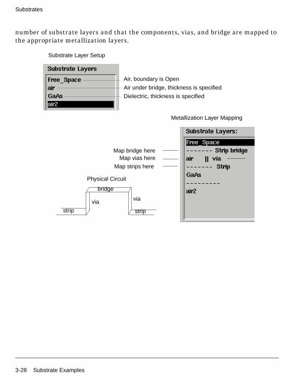
3-28 Substrate Examples
Substrates
number of substrate layers and that the components, vias, and bridge are mapped tothe appropriate metallization layers.
Substrate Layer Setup
Air, boundary is Open
Air under bridge, thickness is specified
Dielectric, thickness is specified
Metallization Layer Mapping
Map bridge hereMap vias here
Map strips here
Physical Circuit
bridge
via via
strip strip

Applying Vias 3-29
Applying ViasMomentum creates a via by extruding the object that is mapped as via through thesubstrate layer it is applied to. So, for example, for a sheet via, you draw a line, for acylinder via you draw a circle. When the shape is mapped to a via in Momentum,another dimension is added to the object in order for the shape to cut through thesubstrate. Thus a line becomes a sheet, a circle becomes a cylinder.
Regardless of how you draw vias, avoid having them extend over the sides of theobjects that they connect to. Vias must be on the edge or inside the object. Anyportion of the via outside of the object boundaries will not be taken into accountduring the simulation. The figure here illustrates vias connecting two strips.
Vias can be applied to multiple layers so that they cut through one or more layers.
representations ofvias in Layout
strip strip
viavia
bridge
via
vias extruded througha substrate layer inMomentum
Circular Via:Correct, but may not be efficient.Use an appropriate arcrecognition.
Incorrect.Via overlaps the object edges.
Efficient via:Sheet via with widthmatching width of strip.
Correct, but not as efficient assheet via with matching widthto strip.

3-30 Applying Vias
Substrates

Adding a Port to a Circuit 4-1
Chapter 4: PortsPorts enable energy to flow into and out of a circuit. Energy is applied to a circuit aspart of the simulation process. A circuit solved using Momentum can have, at theminimum, one port.
Ports are defined in a two-step process. First, ports are added to a circuit when thecircuit is drawn. Then, in Momentum, you specify the type of port in order to tailorthe port to your circuit. This facilitates the simulation process.
This chapter begins with suggestions to keep in mind when adding ports to a circuitthat will be simulated using Momentum. The remainder of this chapter describes thevarious port types in Momentum and gives instructions on how to specify a port type.
Adding a Port to a CircuitYou can add a port to a circuit either from the Schematic window or a Layout window.For instructions on how to add a port to a circuit, refer to “Adding a Port to a Circuit”on page B-4. The procedures include considerations for adding ports to a circuit thatwill be simulated using Momentum.
Considerations
Keep the following points in mind when adding ports to circuits to be simulated usingMomentum:
• The components or shapes that ports are connected to must be on layout layersthat are mapped to metallization layers that are defined as strips or slots. Portscannot be directly connected to vias. For information on how to define strips andslots, refer to “Defining Metallization Layers” on page 3-12.
• Make sure that ports on edges are positioned so that the arrow is outside of theobject, pointing inwards, and at a straight angle.
• Make sure that the port and the object you are connecting it to are on the samelayout layer. For convenience, you can set the entry layer to this layer; theEntry Layer listbox is on the Layout tool bar.
• A port must be applied to an object. If a port is applied in open space so that isnot connected to an object, Momentum will automatically snap the port to theedge of the closest object. This will not be apparent from the layout, however,because the position of the port will not change.
4-2 Determining the Port Type to Use
Ports
• If the Layout resolution is changed after adding ports that are snapped to edges,you must delete the ports and add them again. The resolution change makes itunclear to which edges the ports are snapped, causing errors in meshcalculations.
Note Do not use the ground port component (Component > Ground) in circuits thatwill be simulated using Momentum. Either add ground planes to the substrate or usethe ground reference ports that are described later in this chapter.
Ground port component toolbar button:
Determining the Port Type to UseThere are five port types in Momentum. The purpose of ports is to inject energy into acircuit and to allow energy to flow into and out of a circuit. The different port typesenable you to tailor the ports in your circuit according to your type of circuit and itsfunction in the circuit. In general, you should select the port type that best matchesthe intended application of your layout.
The table below gives a brief description of each port type. You can use a combinationof port types in your circuit, although note that port types have limitations on wherethey can be applied. Only the Single port type can be applied to objects that are oneither strip or slot metallization layers. Only the Internal and Ground Referencetypes can be applied to ports that are on the surface of an object, the remaining typescan be applied to ports that are connected to an edge of an object.
Note Strips and slots refer to metallization layers. For more information on theselayers, refer to “Defining Metallization Layers” on page 3-12.
If you elect not to assign port types, any port in the circuit will be treated as a Singleport type during simulation.
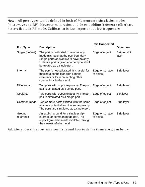
Determining the Port Type to Use 4-3
Note All port types can be defined in both of Momentum’s simulation modes(microwave and RF). However, calibration and de-embedding (reference offset) arenot available in RF mode. Calibration is less important at low frequencies.
Additional details about each port type and how to define them are given below.
Port Type DescriptionPort Connectedto Object on
Single (default) The port is calibrated to remove anymode mismatch at the port boundary.Single ports on slot layers have polarity.Unless a port is given another type, it willbe treated as a single port.
Edge of object Strip or slotlayer
Internal The port is not calibrated. It is useful formaking a connection with lumpedelements or for representing otherconnections in the circuit.
Edge or surfaceof object
Strip layer
Differential Two ports with opposite polarity. The portpair is simulated as a single port.
Edge of object Strip layer
Coplanar Two ports with opposite polarity. The portpair is simulated as a single port.
Edge of object Slot layer
Common mode Two or more ports excited with the sameabsolute potential and the same polarity.The ports are simulated as a single port.
Edge of object Strip layer
Groundreference
An explicit ground for a single (strip),internal, or common mode port.Theimplicit ground is made available throughthe closest infinite metal.
Edge or surfaceof object
Strip layer

4-4 Defining a Single Port
Ports
Defining a Single PortSingle is the default port type. It has the following properties:
• It is connected to an object that is on either a strip or slot metallization layer.
• It can be applied only to the edge of an object.
• The port is external and calibrated. The port is excited using a calibrationprocess that removes any undesired reactive effects of the port excitations(mode mismatch) at the port boundary. This is performed by extending the portboundary with a half-wavelength calibration (transmission) line. The frequencywavelength selected during the mesh or simulation process is used to calculatethe length of the calibration line. For more information about the calibrationprocess, refer to “Calibration and De-embedding of the S-parameters” onpage A-8.
• The port boundary can be moved into or away from the geometry by specifying areference offset. S-parameters will be calculated as if the port were at thisposition. For more information, refer to “Applying Reference Offsets” onpage 4-6.
• When two or more single ports are on the same reference plane, coupling effectscaused by parasitics affects the S-parameters. The calibration process groupsthe ports so that any coupling in the calibration arms is included in theS-parameter solution. For more information, refer to “Allowing for CouplingEffects” on page 4-9.
• If the port is connected to an object on a strip layer, the substrate definitionmust include at least one infinite metal layer: a top cover, ground plane, or aslot layer, or a ground reference must be used in addition to the port. For moreinformation on ground references, refer to “Defining a Ground Reference” onpage 4-18.
• If the port is connected to an object that is on a slot layer, the port has polarity.

Defining a Single Port 4-5
Tip It is not necessary to open the Port Editor dialog box to assign this porttype. Any port without a port type specified is assumed to be a single port.
To define a single port type:
1. Choose Momentum > Port Editor .
2. Select the port that you want to assign this type to.
3. In the Port Editor dialog box, under Port Type, select Single.
4. Enter the components of the port impedance in the Real and Imaginary fields,and specify the units.
5. You can shift the port boundary, also referred to as the port reference plane.Shifting the boundary enables a type of de-embedding process that effectivelyadds or subtracts electrical length from the circuit, based on the characteristicimpedance and propagation characteristic of the port. Enter the offset in theReference Offset field, and select the units. A positive value moves the portboundary into the circuit, a negative value moves the port boundary away fromthe circuit.
6. Click Apply to add the definition to the port.
Physical port boundary
Calibration armremoves mismatch
p1
p2

4-6 Defining a Single Port
Ports
Avoiding Overlap
Be aware that when using single ports, the calibration arm applied to a port may belong enough to overlap another element in the circuit. In this case, the port will bechanged to an internal port type, and no calibration will be performed on it. If thisoccurs, a message will be displayed during simulation in the Status windowindicating the change. For information about internal ports, refer to “Defining anInternal Port” on page 4-10.
Applying Reference Offsets
Reference offsets enable you to reposition single port types in a layout and therebyadjust electrical lengths in a layout, without changing the actual drawing.S-parameters are returned as if the ports were placed at the position of the referenceoffset.
p1
p2
The calibration arm overlaps thestrip. An internal port will beused instead.
p1 p2p1 p2
S-parameters will becalculated based on thepositions of p1 and p2
S-parameters will be calculated as ifp1 and p2 were positioned at thereference offsets
no reference offset reference offsetsapplied to p1 and p2

Defining a Single Port 4-7
Why Use Reference Offsets?
The need to adjust the position of ports in a layout is analogous to the need toeliminate the effect of probes when measuring hardware prototypes. When hardwareprototypes are measured, probes are connected to the input and output leads of theDevice Under Test (DUT). These probes feed energy to the DUT, and measure theresponse of the circuit. Unfortunately, the measured response characterizes the entiresetup, that is, the DUT plus the probes. This is an unwanted effect. The finalmeasurements should reflect the characteristics of the DUT alone. Thecharacteristics of the probes are well known, so measurement labs canmathematically eliminate the effects of the probes, and present the correctmeasurements of the DUT.
There are significant resemblances between this hardware measurement process andthe way Momentum operates. In the case of Momentum, the probes are replaced byports, which, during simulation, will feed energy to the circuit and measure itsresponse. The Momentum port feeding scheme also has its own, unwanted effect:low-order mode mismatch at the port's boundary, although this is eliminated by thecalibration process. However, in order for this calibration process to work well, it isnecessary that the fundamental mode is characterized accurately. This can only beaccomplished when the distance between the port boundary and the firstdiscontinuity is sufficiently large, that is, there exists a feedline that is long enoughto provide this distance.
As a basic example, consider a linewidth that varies abruptly in some part of yourcircuit, as shown in the example below.
Strictly speaking, all you need is to characterize is the variation of the step-in-widthitself, as shown below.
p2p1

4-8 Defining a Single Port
Ports
As mentioned previously, it takes a little distance for the fundamental mode to settle,which means that this “short” structure might not yield the accuracy that you expectfrom an Momentum simulation. In this case, allow for some feed line length:
Now the simulation will yield accurate results, but the results will also contain theextra line lengths. To remedy this, use reference offsets. Although the circuit hasbeen calculated with the long lines, reference offset shifting allows you to produce theS-parameters as if the short structure had been simulated instead:
The effect of the extra feed lines is mathematically eliminated from the S-parametersolution.
This process of adding or subtracting line length is generally referred to asde-embedding. This is the basic process:
During the solution process, the impedance and propagation constant has beencalculated for the ports, based on their physical location in the circuit. When youknow the impedance, propagation constant, and the distance of de-embedding, youcan cancel out the extra lengths of line from the S-parameter results, bycompensating for the loss and phase shifts of those lines. The net result is a set ofS-parameters, calculated as if the extra line lengths were not there.
De-embedding Considerations
It is possible to de-embed right up to the discontinuity itself. However, make surethat you do not shift the reference offset beyond the first discontinuity. This wouldyield incorrect simulation results, as there is another linewidth beyond thatdiscontinuity, which means that there is another set of impedance and propagationvalues that applies there.
p2p1
p1 p2
apply reference offsets atthese locations

Defining a Single Port 4-9
Note You can de-embed away from the circuit, by placing reference offsets beyondthe edges of the layout. This enables you to simulate the effect of a long feed line thatwas not drawn in the simulated structure.
Note that for calculation speed purposes, the impedance and propagation constant forgrouped ports are approximated instead of explicitly calculated. The only way to haveimpedance and propagation constant explicitly calculated in all cases is to de-embedsome small distance. This will cause some lengthy calculations, but the resultsshould be more accurate for users who want to look at accurate impedance andpropagation constants.
Allowing for Coupling Effects
If you have two or more single ports that lie on the same reference plane, thecalibration process will take into account the coupling caused by parasitics thatnaturally occurs between these ports. This yields simulation results that moreaccurately reflect the behavior of an actual circuit.
The figure below helps illustrate which ports will be grouped in order for thecalibration process to account for coupling among the ports. In this setup, only thefirst two ports will be grouped, since the third port is an internal port type and thefourth port is on a different reference plane. Note that even though the second porthas a reference offset assigned to it, for this process they are considered to be on thesame plane and their reference offsets will be made equal.

4-10 Defining an Internal Port
Ports
If you do not want the ports to be grouped, you must add a small thickness of metal tothe edge of the object that one of the ports is connected to. The ports will no longer beon the same plane, and will not be considered part of the same group.
Defining an Internal PortInternal ports enable you to apply a port to the surface of an object in your design. Byusing internal ports, all of the physical connections in a circuit can be represented, soyour simulation can take into account all of the EM coupling effects that will occuramong ports in the circuit. These coupling effects caused by parasitics are included inyour simulation results because internal ports are not calibrated. You should avoidgeometries that allow coupling between single and internal ports to prevent incorrectS-parameters.
An example of where an internal port is useful is to simulate a bond wire on thesurface on an object. Another example of where an internal port is necessary is acircuit that consists of transmission lines that connect to a device, such as atransistor or a chip capacitor, but this device is not part of the circuit that you aresimulating. An internal port can be placed at the connection point, so even though thedevice is not part of the circuit you are simulating, the coupling effects that occuramong the ports and around the device will be included in your simulation.
Internal ports are often used in conjunction with ground references. For moreinformation, refer to “Defining a Ground Reference” on page 4-18 and to “Simulatingwith Internal Ports and Ground References” on page A-10.
port 1
port 2
port 3
port 4
reference plane
single
single, withreference offset
internal
single

Defining an Internal Port 4-11
An internal port type has the following properties:
• It can be applied to the interior of a circuit by applying it to the surface of anobject.
• It can be applied to the edge of an object.
• It can be applied to objects that are on strip layers only.
• The orientation of the port is not considered if it is on the surface of an object.(For a description of port orientation, refer to “Adding a Port to a Layout” onpage B-5.)
• No calibration is performed on the port.
• The reference impedance for internal ports is 50 ohms.
Because no calibration is performed on the port, the results will not be as accurate aswith a single port. However, the difference in accuracy is small.
To define an internal port:
1. Choose Momentum > Port Editor .
2. Select the port that you want to assign this type to.
3. Click Apply .
Ports 1 and 2 areinternal ports
1
2
3
4
5

4-12 Defining a Differential Port
Ports
Defining a Differential PortDifferential ports should be used in situations where an electric field is likely to buildup between two ports (odd modes propagate). This can occur when:
• The two ports are close together
• There is no ground plane in the circuit or the ground plane is relatively faraway
• One port behaves (to a degree) like a ground to the other port, and polaritybetween the ports is developed.
• The ports are connected to objects that are on strip metallization layers.
The electric field that builds up between the two ports will have an effect on thecircuit that should be taken into account during a simulation. To do this, usedifferential ports.
Differential ports have the following properties:
• They can be applied to objects on strip layers only.
• They are assigned in pairs, and each pair is assigned a single port number.
• Each of the two ports is excited with the same absolute potential, but with theopposite polarity. The voltages are opposite (180 degrees out of phase). Thecurrents are equal but opposite in direction when the ports are on twosymmetrical lines, and the current direction is approximated for otherconfigurations.

Defining a Differential Port 4-13
• The two ports must be on the same reference plane.
Note Port numbers for differential ports are treated in the following manner: on thelayout, you will continue to see the port numbers (instance names) that wereassigned to each port when they were added to the layout. Use the Momentum PortEditor dialog box to identify which pair of ports will be treated as a differential port.
Also, when you view results, you will see S-parameters for the differential portnumbers. In the example above, the layout would show p1, p2, p3, p4. TheS-parameter results will be for combinations of P1 and P3 only.
To define a differential port:
1. Choose Momentum > Port Editor .
2. Select the port that you want to assign this type to. Note the port number.
3. In the Port Editor dialog box, under Port Type, select Differential .
4. Under Polarity, make sure that Normal is selected.
5. Click Apply .
An electric field will likelybuild up between these twolines. Assign the ports asdifferential ports. They willbe treated as one port andassigned the same portnumber.
Assign as differential ports. They willbe treated as one port and assignedthe same port number.
strip port 1 +
strip port 1 _
port 3 +
port 3
_

4-14 Defining a Coplanar Port
Ports
6. Select the second port.
7. In the Port Editor dialog box, under Port Type, select Differential .
8. Under Polarity, select Reversed .
9. Under Associate with port number, enter the number of the previously-selectedport.
10. Click Apply .
11. Repeat these steps for other differential port pairs in the circuit.
12. Click OK to dismiss the dialog box.
Defining a Coplanar PortThis type of port is used specifically for coplanar waveguide (CPW) circuits. It issimilar to a differential port, but coplanar ports are applied to objects on slot layers(that is, where slots are used in the design). Coplanar ports should be used insituations where an electric field is likely to build up between two ports. This canoccur when:
• The two ports are close together
• Polarity between the ports develops
• The ports are connected to objects that are on slot metallization layers
The electric field that builds up between the two ports will have an effect on thecircuit that should be taken into account during a simulation. To do this, use coplanarports.
Coplanar ports have the following properties:
• They can be applied to objects on slot layers only.
• They are assigned in pairs.
• Each of the two ports is excited with the same absolute potential, but with theopposite polarity. The voltages are opposite (180 degrees out of phase). Thecurrents are equal but opposite in direction when the ports are on twosymmetrical lines, and the current direction is approximated for otherconfigurations.
• The two ports must be on the same reference plane.

Defining a Coplanar Port 4-15
The illustration below shows ports pairs applied to a layout of coplanar waveguideslots. The coplanar port type is applied to each pair of ports in the design. The arrowsin this illustration indicate the polarity assigned to each port and the direction of thevoltages over the slots (arrows indicate the direction of the voltages).
Note Port numbers for coplanar ports are treated in the following manner: on thelayout, you will continue to see the port numbers (instance names) that wereassigned to each port when they were added to the layout. Use the Momentum PortEditor dialog box to identify which pair of ports will be treated as a coplanar port.
Also, when you view results, you will see S-parameters for the coplanar portnumbers. In the example above, the layout would show p1, p2, p3, p4. TheS-parameter results will be for combinations of P1 and P3 only.
Be careful when assigning polarity to coplanar ports. An incorrect choice of polaritycan change the phase of transmission type S-parameters by 180 degrees. To verifypolarity, zoom in on a coplanar port. You will notice two sets of arrows applied to theport. One appears when you add the port component to the circuit. The second will
—
—
+
+ ——
groundplanes
slots
port 3(normalpolarity)
port 3(reversedpolarity)
Arrows indicate orientation (polarity) ofthe voltages over the slots.
(reversed polarity)port 1
port 1(normal polarity)

4-16 Defining a Coplanar Port
Ports
appear after the mesh is computed. It indicates the direction of the voltage over theslot.
To define coplanar ports:
Note Coplanar ports can be applied to objects on slot layers only.
1. Choose Momentum > Port Editor .
2. Select the port that you want to assign this type to. Note the port number.
3. In the Port Editor dialog box, under Port Type, select Coplanar .
4. Under Polarity, make sure that Normal is selected.
5. Click Apply .
6. Select the second port.
7. In the Port Editor dialog box, under Port Type, select Coplanar .
8. Under Polarity, select Reversed .
9. Under Associate with port number, enter the number of the previously-selectedport.
10. Click Apply .
11. Repeat these steps for other differential port pairs in the circuit.
12. Click OK to dismiss the dialog box.
This arrow appears afterthe mesh is computed andindicates the direction ofthe voltage over the slot.
This arrow is part ofthe port component

Defining a Common Mode Port 4-17
Defining a Common Mode PortUse common mode ports in designs where the polarity of fields is the same amongtwo or more ports (even modes propagate). The associated ports are excited with thesame absolute potential and are given the same port number.
Common mode ports have the following properties:
• They can be applied to objects on strip layers only
• A ground plane or other infinite metal (such as a cover) is required as part ofthe design
• Two or more ports can be associated
• Associated ports are excited with the same absolute potential (and samepolarity)
• The ports must be on the same reference plane
Note Port numbers for common ports are treated in the following manner: on thelayout, you will continue to see the port numbers (instance names) that wereassigned to each port when they were added to the layout. Use the Momentum PortEditor dialog box to identify which group of ports will be treated as a common port.
Also, when you view results, you will see S-parameters for the common port numbers.In the example above, the layout would show p1, p2, p3. The S-parameter results willbe for combinations of P1 only.
To define a common port:
Three ports are treated as one after they areassociated as common mode ports.
Before After
p1
p2
p3
p1
p1
p1

4-18 Defining a Ground Reference
Ports
1. Choose Momentum > Port Editor .
2. Select the port that you want to assign this type to. Note the port number.
3. In the Port Editor dialog box, under Port Type, select Common Mode .
4. Click Apply .
5. Select the second port.
6. In the Port Editor dialog box, under Port Type, select Common Mode .
7. Under Associate with port number, enter the number of the port that youselected first.
Make sure that the value in the Associate with port number field is the same foradditional ports. For example, if you were associating three ports and the first portwas assigned as port 1, for the second and third port, the value entered into theAssociate with port number field would be 1. (For the first port you choose, novalue is entered in this field.)
8. Click Apply .
9. Repeat these steps for other common mode ports in the circuit.
10. Click OK to dismiss the dialog box.
Defining a Ground ReferenceGround references enable you to add explicit ground references to a circuit, whichmay be necessary if implicit grounds are in your design.
Implicit ground is the potential at infinity, and it is made available to the circuitthrough the closest infinite metal layer of the substrate. Implicit grounds are usedwith internal ports and with single ports that are connected to objects on stripmetallization layers.
There are instances where the distance between a port and its implicit ground is toolarge electrically, or there are no infinite metal layers defined in the substrate. Inthese cases, you need to add explicit ground references to ensure accurate simulationresults. For more information on using ground references, refer to “Simulating withInternal Ports and Ground References” on page A-10.
You can apply ground references to the surfaces of object. The object must be on stripmetallization layers.

Editing a Port 4-19
Note Multiple ground reference ports can be associated with the same port. To beassociated with a single port, the ground reference port should be a port attached toan edge of an object in the same reference plane as the single port.
To add a ground reference:
1. Choose Momentum > Port Editor .
2. Select the port that you want to assign as the ground reference.
3. In the Port Editor dialog box, under Port Type, select Ground Reference .
4. Under Associate with port number , enter the number of the single or internalport that you want to associate with this ground reference. Make sure that thedistance between the port and ground reference is electrically small.
5. Click Apply .
Editing a PortFor best results, use the Port Editor (Momentum > Port Editor... ) to change portproperties. You edit the port in the same manner as when you entered the initialdefinition.
Note Be aware that it is possible to edit port properties by selecting the port andchoosing Edit > Properties from the Layout menu bar, however, this method is notrecommended.
For more information on setting port definitions see the appropriate section:
“Defining a Single Port” on page 4-4
“Defining an Internal Port” on page 4-10
“Defining a Differential Port” on page 4-12
“Defining a Coplanar Port” on page 4-14
“Defining a Common Mode Port” on page 4-17

4-20 Remapping Port Numbers
Ports
Remapping Port NumbersSome designs contain non-consecutive port numbers. This results in simulation datafiles that are difficult to use. When Momentum simulates designs containingnon-consecutive port numbers, the ports are remapped to consecutive numbers in theresulting data file. The lowest port number is remapped to 1, and remaining numbersare remapped in consecutive order. The port numbers are not changed in the designitself. A message in the Status window announces the change, and lists the mappings.
For example, if you are simulating a design with ports numbered 37 and 101, thefollowing status message informs you of the changes:
Layout has non-consecutive port numbers.Output files will have consecutive port numbers.
layout port -> output port37 -> 1101 -> 2
Port number remapping is done only for sampled and AFS CITIfiles and theircorresponding S-parameter datasets. It is not done for Visualization and far fieldfiles. The remapping is done at the CITIfile level, and propagates to the dataset file.After remapping, all datasets are in sync with the new port numbering.

5-1
Chapter 5: Boxes and WaveguidesWhen you specified the substrate definition of a circuit (from the Momentum >Substrate menu), you specified only the vertical dimension of the substrate and notthe horizontal dimension. Given this definition, the substrate layers extend all theway to infinity in the horizontal direction. For many circuit designs this is notrelevant and does not affect the simulation. However, there may be instances whereyou want to introduce horizontal boundaries. For these instances, you can use boxesor waveguides.
Boxes and waveguides enable you to specify substrate boundaries in the horizontaldirection. A box enables you to set boundaries on four sides of the substrate. Awaveguide enables you to set boundaries on two sides. These effects are availableonly when using the Momentum (microwave) simulation mode, and not with theMomentum RF mode.
More specifically, for a box, you define four, perpendicular vertical planes of perfectmetal as the horizontal boundaries of the substrate. These four vertical planes, orwalls, form a rectangle, if you are looking at the circuit from the top, along the z-axis.A box can be used only where the top and bottom layers in the substrate definitionare groundplanes or impedance termination. Thus, the four vertical metal walls, plusthe top and bottom groundplanes result in a box, hence the name (the walls are thesides, and the top and bottom ground planes are lid and base of the box).
A waveguide is similar, although for a waveguide you specify only two parallel walls.The substrate is therefore only bounded in the horizontal direction perpendicular to
box
A box can represent a highly resonantmetallic enclosure. Its effect will be takeninto account during simulation.

5-2 Adding a Box
Boxes and Waveguides
these walls. In the horizontal direction parallel to these walls, the substrate stillextends to infinity. The top and bottom layers of the substrate must also be defined asgroundplanes. The two sidewalls in combination and the top and bottom covers forma waveguide.
The next section describes how to apply a box or waveguide to a circuit. For moreinformation about applications for these items, refer to “About Boxes andWaveguides” on page 5-5.
Adding a BoxA box defines the boundaries on four sides of the circuit substrate. Either one box orone waveguide can be applied to a circuit at a time. A box can be applied to a circuitonly if the top and bottom layers of the substrate definition are defined asgroundplanes or impedance termination. The walls of the box are perfect metal. Theground planes can be defined either as perfect metals or a lossy metal.
Adding a box to the circuit enables you to analyze the effects of enclosing the circuitin metal, for example, to identify box resonance. Box resonance can have a significanteffect on S-parameters in a small band centered around the box resonance frequency.When a simulation is performed, the resonance frequencies will be noted in thestatus window when the circuit is simulated, along with the frequency bands whereno smooth S-parameters can be calculated.
During a simulation, all current directions on the sidewalls of the box are taken intoaccount.
A waveguide enables you to take into account theeffects of sidewalls near the circuit, or verify thatsidewalls do not affect your design.waveguide

Adding a Box 5-3
To add a box:
1. Choose Momentum > Box-Waveguide > Add Box .
2. Draw the box using one of the following two methods:
• Position the mouse and click to define a corner of the box. Move the mouse tothe diagonal corner and click.
• From the Layout menu bar choose Draw > Coordinate Entry and use theCoordinate Entry X and Coordinate Entry Y fields to specify a corner of thebox. Click Apply . Enter the coordinates of the diagonal corner and click Apply .Click Cancel to dismiss the dialog box.
The box is displayed in the layout.
Editing a Box
Once the box is applied, you cannot change its dimensions. If you want to change thesize, you must delete the current box and add a new one.
Deleting a Box
To delete a box:
1. Choose Momentum > Box-Waveguide > Delete Box .
The box is removed from the layout.
Viewing Layout Layer Settings of a Box
The box is defined as a layout layer named momentum_box. You may review thelayout layer settings, but it is a protected layer, so you should not change the settingsof this layer.
To view the box layer specifications:
1. Choose Options > Layers .
2. Select momentum_box from the Layers list. The layer settings are displayed. Formore information on these parameters, refer to the Layout manual.
3. Click Cancel to dismiss the dialog box.

5-4 Adding a Waveguide
Boxes and Waveguides
Adding a WaveguideA waveguide defines the boundaries on two, parallel sides of the circuit substrate.Either one box or one waveguide can be applied to a circuit at a time. A waveguidecan be applied to a circuit only if the top and bottom layers of the substrate definitionare defined as groundplanes or impedance termination. The walls of the waveguideare perfect metal. The ground planes can be defined either as perfect metals or metalwith loss.
During a simulation, all current directions on the sidewalls of the waveguide. aretaken into account.
To add a waveguide:
1. Choose Momentum > Box-Waveguide > Add Waveguide .
2. Select the direction of the waveguide. To draw the waveguide parallel to thex-axis, click X-axis . To draw the waveguide parallel to the y-axis, click Y-axis .
3. Draw the waveguide using one of the following two methods:
• Position the mouse and click to define one wall of the waveguide. Move themouse to the position of a point on the second wall and click.
• From the Layout menu bar choose Draw > Coordinate Entry and use theCoordinate Entry X and Coordinate Entry Y fields to specify a point on theedge of the substrate. Click Apply . Enter the coordinates of a point on thesecond, parallel edge of the substrate and click Apply . Click Cancel to dismissthe dialog box.
These boundaries specify the edges of the substrate and the width of the waveguide.
Editing a Waveguide
Once the waveguide is applied, you cannot change its dimensions. If you want tochange the size, you must delete the current waveguide and add a new one.
Deleting a Waveguide
To delete a waveguide:
1. Choose Momentum > Box-Waveguide > Delete Waveguide .
The waveguide is removed from the layout.

About Boxes and Waveguides 5-5
Viewing Layout Layer Settings of a Waveguide
The waveguide is defined as a layout layer named momentum_box. You may reviewthe layout layer settings, but it is a protected layer, so you should not change thesettings of this layer.
To view the waveguide layer specifications:
1. Choose Options > Layers .
2. Select momentum_box from the Layers list. The layer settings are displayed. Formore information on these parameters, refer to the Layout manual.
3. Click Cancel to dismiss the dialog box.
About Boxes and WaveguidesThere are a variety of reasons why you would want to simulate a circuit in a box orwaveguide:
• The actual circuit is enclosed in a metal box
• Nearby metal sidewalls may affect circuit performance
• The box may resonate
• Propagating modes may be present
These situations are discussed next.
Circuits are often encased in metal enclosures. By adding a box to your design, themetal sidewalls that are present in the real structure may be included in thesimulation. This is useful is you suspect that the presence of these sidewalls will havean immediate effect on the behavior of the circuit. For example, “broad-coupledfilters” are placed in metal enclosures (a box) and the sidewalls can have ansignificant influence on the filter characteristics.
You may want to use a box or waveguide because metal sidewalls are present in thereal structure and there may be an effect from these sidewalls on the characteristicsof the circuit. This can be a parasitic, unwanted effect. If the effects of the sidewallswere not taken into account while designing the circuit, you can verify any effect thatthe sidewalls may have on your circuit. In most cases, when the sidewalls are not tooclose to the actual circuit, the effect of the sidewalls on the simulation results will bemarginal. There is, however a specific, significant condition, which is unique forstructures with sidewalls.

5-6 About Boxes and Waveguides
Boxes and Waveguides
In the case of a box, this is the occurrence of one or more box resonances. A boxresonance is a physical effect where, under the condition of certain frequency and boxsize combinations, the box actually starts resonating at a certain frequency. Becausea box resonance has a significant effect on S-parameters in a (small) band centeredaround the box resonance frequency which cannot be represented by a smoothfunction, no smooth adaptive S-parameters will be available in this frequency band.When simulating such a circuit, Momentum will inform you of these box resonancefrequencies, of the frequency bands where there will not be smooth S-parametersavailable and of the quality factor (a measure for the sharpness of the box resonance,depending on the losses).
In the case of waveguide, the effect is the excitation of a waveguide mode. If yourcircuit will be positioned near sidewalls, you may want to add a waveguide todetermine whether they have an effect on the performance of the circuit.
You may have a situation where there are no metal sidewalls in the structure, but thesubstrate definition is bounded by other material (for example, you have a finite-sizesubstrate where the dielectric material abruptly ends, so you have a dielectric-airtransition). Although Momentum boxes and waveguides are defined as perfect metalsand not dielectric material, you may decide that defining a metallic enclosure in thesimulated circuit may be more representative of the real structure than using noenclosure.
Adding Absorbing Layers under a Cover
You may want to model your box or waveguide as having absorbing layers betweenthe covers and the layout. You can use a substrate interface layer, define itsthickness, and its absorbing properties using ε and µ (make sure that ε and µ areaccurate specifications for this layer). Adding absorbing layers to a box would have aneffect on any box resonances that would occur by producing a weaker resonance, thatis, the quality factor of the box resonances would lower significantly.
Boxes, Waveguides, and Radiation Patterns
If you have a structure enclosed in a box or waveguide and you want to calculateradiation patterns for it after the simulation, you need to set the top and bottomplanes to values between 376 and 378. There are also other considerations. For moreinformation, refer to “377 Ohm Terminations and Radiation Patterns” on page 3-26.

6-1
Chapter 6: MeshA mesh is a grid-like pattern of triangles and rectangles, and each triangle orrectangle is a cell. This pattern of cells is based on the geometry of a circuit and,optionally, user-defined parameters, so each circuit will have a unique meshcalculated for it. The mesh is then applied to the circuit in order to compute thecurrent within each cell and identify any coupling effects in the circuit duringsimulation. From these calculations, S-parameters are then calculated for the circuit.The mesh that was calculated for the double patch example is shown below.
Creating a mesh consists of two parts:
• Defining mesh parameters
• Precomputing the mesh
It is not necessary to set up mesh parameters; default parameters will be usedinstead. You can precompute the mesh before simulating in order to view the mesh,otherwise the mesh will be computed as part of the simulation process. A mesh isrequired in order to simulate.
This chapter describes how to define mesh parameters and calculate the mesh. It alsoincludes a description of how the mesh generator works and gives guidelines forsetting mesh parameters for different applications.
Rectangular cells areapplied to most of thegeometry...
...but for curved ornon-rectangular objects,triangles are used to complete

6-2 Defining a Mesh
Mesh
Defining a MeshChoose Momentum > Mesh > Setup to set up mesh parameters, which enable you tocontrol the number of cells that are used to create the mesh. The more cells, the moreaccurate the simulation will be, but too many cells will slow down a simulation andprovide little improvement in accuracy. You can choose not to set up meshparameters, and default values will be used to create the mesh.
If you choose to define mesh parameters, you can set them for:
• The entire circuit
• The objects on a layout layer
• A single object
It is not necessary to specify parameters for all levels. You can, for example, specifymesh parameters for a single object, and use default values for the rest of the circuit.
For more information about how a mesh is generated, refer to “About the MeshGenerator” on page 6-13. For suggestions to consider when setting mesh parameters,refer to “Guidelines for Meshing” on page 6-23.
Procedures for setting up mesh parameters follow.
Defining Mesh Parameters for the Entire Circuit
Global mesh parameters affect the entire circuit. To set up global parameters:
1. Choose Momentum > Mesh > Setup .
2. The Global parameters are displayed.
3. Enter the mesh frequency in the Mesh Frequency field and select the units. Thewavelength of this frequency will be used to determine the density of the mesh.In general, set the value of the mesh frequency to the highest frequency thatwill be simulated. For more information, refer to “Adjusting Mesh Density” onpage 6-14.
4. Enter the Number of Cells per Wavelength. This value will also be used todetermine the density of the mesh. The relationship between wavelength andcells per wavelength can be described by example: if the circuit is 3 wavelengthslong and the number of cells per wavelength is 20, the length of the circuit willbe divided into 60 cells.For more information, refer to “Adjusting Mesh Density”on page 6-14.

Defining a Mesh 6-3
5. Any curved areas in the circuit will be meshed using facets. In the Arc FacetAngle field, enter the number of degrees that will be included in a single facet.The maximum is 45 degrees per facet. The lower the value, the better theresolution and the denser the mesh will be. The minimum value is equal to theArc/Circle Resolution which is set when the object is drawn. For moreinformation, refer to “Using the Arc Facet Angle” on page 6-19.
6. Enable Edge Mesh to add a relatively dense mesh along the edges of objects.Since most current flows along the edges of objects, the edge mesh can improvethe accuracy and speed of a simulation.
If you want the edge mesh to be sized automatically, leave the Edge Width fieldblank. Otherwise, specify the edge width and select the units. For moreinformation about the edge mesh, refer to “About the Edge Mesh” on page 6-15.
Note An edge mesh that you specify will not be used if the edge width is largerthan the cell size set by the wavelength/number_of_cells_wavelength. This isbecause such edge meshes would be very inefficient. If the edge mesh valuesmust be used, decrease the number_of_cells_wavelength, which is specified inthe Number of Cells per Wavelength field.
7. Enable Transmission Line Mesh to specify the number of cells along the width ofa geometry. It is most useful for circuits with straight-line geometry.
Enter the number of cells that the width will be divided into in the Number ofCells Wide field. This will be the total number of cells along the width of thecircuit. For more information about the transmission mesh, refer to “About theTransmission Line Mesh” on page 6-16.
Arc Facet Angle is 30 degrees Arc Facet Angle is 18 degrees

6-4 Defining a Mesh
Mesh
8. Enable Thin layer overlap extraction in order to extract objects for the followingsituations:
• Two objects on different layers overlap
• The objects are separated with a thin substrate layer
If this is enabled, the geometry will be altered to produce a more accurate modelfor the overlap region. For more information, refer to “Processing Object Overlap”on page 6-21.
Note This should always be enabled when modeling thin layer capacitors.
9. If you want to revert to default parameters, click Reset .
10. Click OK to accept the global mesh parameters.
Defining Mesh Parameters for a Layout Layer
You can define mesh parameters that affect the objects on a single layout layer. If youhave global parameters set, they will not be used where mesh parameters are definedfor a layout layer.
To set up layout layer parameters:
1. Choose Momentum > Mesh > Setup .
2. Click the Layer tab.
3. From the Layout Layer list, select the metallization layer that you want tospecify mesh parameters for.
4. Enter the Number of Cells per Wavelength. This value, along with thewavelength of the frequency specified in the Frequency field, will be used todetermine the density of the mesh. (Recall that the frequency is a globalparameter).
The relationship between wavelength and cells per wavelength is best describedby example. If the portion of the circuit on this layer is 2 wavelengths long andthe number of cells per wavelength is 20, the length of the circuit on this layerwill be divided into 40 cells. For more information, refer to “Adjusting MeshDensity” on page 6-14.

Defining a Mesh 6-5
5. Enable Edge Mesh to add a relatively dense mesh along the edges of the objectson this layer. Since most current flows along the edges of objects, the edge meshcan improve the accuracy and speed of a simulation.
If want the edge mesh to be sized automatically, leave the Edge Width fieldblank. Otherwise, specify the edge width and select the units. For moreinformation about the edge mesh, refer to “About the Edge Mesh” on page 6-15.
6. Enable Transmission Line Mesh to specify the number of cells along the width ofthe geometry on this layer. It is most useful for circuits with straight-linegeometry.
Enter the number of cells that the width will be divided into in the Number ofCells Wide field. This will be the total number of cells along the width of thecircuit on this layer. For more information about the transmission mesh, refer to“About the Transmission Line Mesh” on page 6-16.
7. If you want to change the settings for the selected layer, click Reset to return todefault values or Clear to erase your settings.
8. Select another layer and repeat these steps for setting the mesh parameters.
9. Click OK to accept the mesh parameters for the layers.
Defining Mesh Parameters for an Object
You can define mesh parameters that affect a single object. If you have global orlayout layer parameters set, they will not be used where mesh parameters aredefined for an object.
To set up object parameters:
1. Choose Momentum > Mesh > Setup .
2. Click the Primitive tab.
3. In the Layout window, select the object that you want to specify meshparameters for.

6-6 Defining a Mesh
Mesh
4. Enter the Number of Cells per Wavelength. This value, along with thewavelength of the frequency specified in the Frequency field, will be used todetermine the density of the mesh. (Recall that the frequency is a globalparameter).
The relationship between wavelength and cells per wavelength is best describedby example. If the object is 1/2 wavelengths long and the number of cells perwavelength is 20, the length of the object will be divided into 10 cells. For moreinformation, refer to “Adjusting Mesh Density” on page 6-14.
5. Enable Edge Mesh to add a relatively dense mesh along the edges of the object.Since most current flows along the edges of objects, the edge mesh can improvethe accuracy and speed of a simulation.
If want the edge mesh to be sized automatically, leave the Edge Width fieldblank. Otherwise, specify the edge width and select the units. For moreinformation about the edge mesh, refer to “About the Edge Mesh” on page 6-15.
6. Enable Transmission Line Mesh to specify the number of cells along the width ofthe object. It is most useful for circuits with straight-line geometry.
Enter the number of cells that the width will be divided into in the Number ofCells Wide field. This will be the total number of cells along the width of theobject. For more information about the transmission mesh, refer to “About theTransmission Line Mesh” on page 6-16.
7. If you want to change the settings for the selected object, click Reset to return todefault values or Clear to erase your settings.
8. Select another object and repeat these steps for setting the mesh parameters.
9. Click OK to accept the mesh parameters for the objects.
Seeding an Object
For the majority of circuits, it is not necessary to seed an object, and it is notrecommended because all internal mesh processes will be skipped. If an object isseeded incorrectly, an inefficient mesh will result, affecting simulation speed andaccuracy. You should have a good understanding of electromagnetics andcomputational geometry to be able to use this meshing feature efficiently.

Defining a Mesh 6-7
Primitive seeding enables you to specify the exact number of cells to be applied to ageometry:
• Horizontally, across the o,u-axis
• Vertically, from point V to the o,u-axis
The example below illustrates the position of the o,u-axis and the position of point Vwith respect to OU on a simple shape. Regardless of the object seeding is applied to,OV must be perpendicular to OU in order to create a correct mesh. This mesh wasdefined to be three cells wide along the o,u-axis, and five cells high.
To seed a primitive:
1. Determine the method for entering mesh coordinates. You can:
• Type coordinates directly into the Coordinate Entry dialog box
• Select coordinates by clicking on objects in the Layout window
If you choose select coordinates on the object, make sure that the vertex snapmode is on, and check your other snap modes to make sure that you cancompletely align the mesh with the structure. If snap modes are on when youselect a coordinate, the system will snap to the nearest point that satisfies anenabled snap mode. This means that you may have difficulty aligning the meshwith the object if snap modes other than vertex snap are enabled. Snap modescan be found in the Layout window under the Options menu.
2. If a mesh is displayed on the layout, choose Momentum > Mesh > Clear .
3. Choose Momentum > Mesh > Setup .
Point V
V
O U
3 cells wide across o,u-axis
5 cells wide from V to O

6-8 Defining a Mesh
Mesh
4. Click the Primitive Seed tab.
5. In the Layout window, select the object that you want to seed. If necessary, zoomin.
6. Specify the o,u-axis. The axis determines the orientation of the mesh. Select theaxis using one of the following two methods:
• Position the mouse and click to define the origin of the o,u-axis. Move themouse to the end of the axis and click.
• From the Layout menu bar choose Draw > Coordinate Entry and use theCoordinate Entry X and Coordinate Entry Y fields to specify the origin of theo,u-axis. Click Apply . Enter the coordinates that define the end of the axis andclick Apply .
7. The Primitive Mesh Control dialog box is displayed. Enter the number of cellsthat you want along the o,u-axis.
8. Specify point V. The point must be positioned so that OV is perpendicular to OU.Select the point using one of the following two methods:
• Position the mouse and click to define the point and click.
• From the Layout menu bar choose Draw > Coordinate Entry and use theCoordinate Entry X and Coordinate Entry Y fields to specify the coordinatesof point V. Click Apply .
9. The Primitive Mesh Control dialog box is displayed. Enter the number of cellsthat you want along the ov-line.
10. The following information will appear for the seeded object:
• The number and name of the layout layer that the object is on
• Data describing the seeded object, including the type of object (for example,path or polygon) and its coordinates
• The angle of the o,u-axis with respect to the x-axis
• The length of each cell along the o,u-axis (the distance of OU divided by thenumber of cells)
• The length of each cell along OV (the distance of OV divided by the number ofcells)

Defining a Mesh 6-9
An example is shown below:
11. If you want to change the settings for the selected object, click Clear to eraseyour settings.
12. Click OK to complete the command.
In the illustration below, the o,u-axis is positioned along the base of the polygon, andit is the length of the polygon. The number of cells along the axis is set to three. Thenumber of cells from OU to V is set to five. The resulting mesh is displayed. Any othermesh parameters that had been specified were used in other parts of the circuit.
Mesh Connectivity
If you choose to seed an object, and you have global, layout layer, or object meshparameters set, these other parameters will not be used on the seeded object. Inaddition, the mesh cells must connect in an appropriate way throughout the circuit in
Layer 2 (bot_met):Path (-35.000000, -2.187000) (0.000000, 2.187000) OU angle = 0.000000 deg.
du = 3.483500 mm, dv = 17.632979 mm
layer dataobject data
OU angle
cell sizes
U to V is 5 cells wide.
O to U is 3 cells wide.Also, OU determines theorientation of the mesh.
Remaining area of object ismeshed by connecting vertices.
V
UO

6-10 Defining a Mesh
Mesh
order to achieve accurate results. This is referred to as mesh connectivity. Be awarethat in order to achieve mesh connectivity, the boundaries of seeded regions may betransformed. The only way to correct this is to modify the seeding of the neighboringobjects. If you choose to seed one object, you should consider seeding the entirecircuit.
Which cells are altered to assure connectivity is governed by creating a mesh thatgenerates the fewest number of unknowns.
Resetting and Clearing Mesh Parameters
If you want to change mesh parameter setting, you can:
• Change individual parameters
• Erase a set of mesh parameter values
• Reset mesh parameters to default values
To reset or clear mesh parameters:
1. Choose Momentum > Mesh > Setup .
2. Select the tab, Global, Layout, Primitive, or Primitive Seed, that contains theparameters you want to erase or reset.
3. Choose one of the following options:
• For layout parameters, select the layout layer name.
• For object mesh parameters or seeding, select the object from the Layoutwindow.
Tip You may want to clear the mesh from the layout before attempting toselect an object.
4. Click Clear to erase the settings, or click Reset to set them to default values.
Note If you have trouble selecting an object, exit the dialog box, select the object,then reopen the dialog box.
Precomputing a Mesh 6-11
Precomputing a Mesh
Note In order to calculate a mesh, you must first precompute the substrate andapply ports to the circuit. For information on how to precompute the substrate, referto Chapter 3, Substrates. For information on how to apply ports, refer to “Adding aPort to a Circuit” on page B-4, and to Chapter 4, Ports.
Choose Momentum > Mesh > Precompute to calculate the mesh. Using the specifiedfrequency and any user-defined mesh parameters, a pattern of rectangles andtriangles is computed and applied to the circuit. During a simulation, the surfacecurrent in each cell is calculated, and this information is then used to solveS-parameters for the structure.
To precompute the mesh:
1. Choose Momentum > Mesh > Precompute .
2. In the Precompute Mesh dialog box, enter the frequency you want to use forprecomputing the mesh. The wavelength of this frequency will, in part,determine the number of cells in the mesh. For more information about meshcalculations, refer to “About the Mesh Generator” on page 6-13.
3. Click OK to start calculating the mesh.
When the computations are complete, the mesh will be displayed on the layout.
Viewing Mesh Status
After mesh computations have started, any messages regarding the computationswill appear in the Momentum Status window. Messages usually refer to any errors orwarnings, or indicate when the mesh is complete.
If you close the status window and want to reopen it, from the Layout menu barchoose Window > Restore Status.

6-12 Stopping Mesh Computations
Mesh
Stopping Mesh ComputationsTo stop the mesh process:
1. From the Momentum Status window, choose Simulation/Synthesis > StopSimulation .
The mesh computations will stop and no information will be saved.
Viewing the Mesh SummaryIf the mesh computation is successful, you can view mesh statistics. Some of theinformation returned includes:
• The number of rectangular cells in the structure
• The number of triangular cells
• The number of vertical rectangular cells used to model the vias
• The number of unknown currents
• Computer resources used and time to solve
The number of cells and the number of unknown currents will affect simulation time.The more cells, the denser the mesh, and the longer the simulation will be. Eachunknown current is a variable in the matrix equation that is solved by the simulator.The greater the number of unknown currents, the larger the matrix, and the longerthe simulation time will be. The memory required to solve the structure increases aswell.
An example of mesh statistics follows.
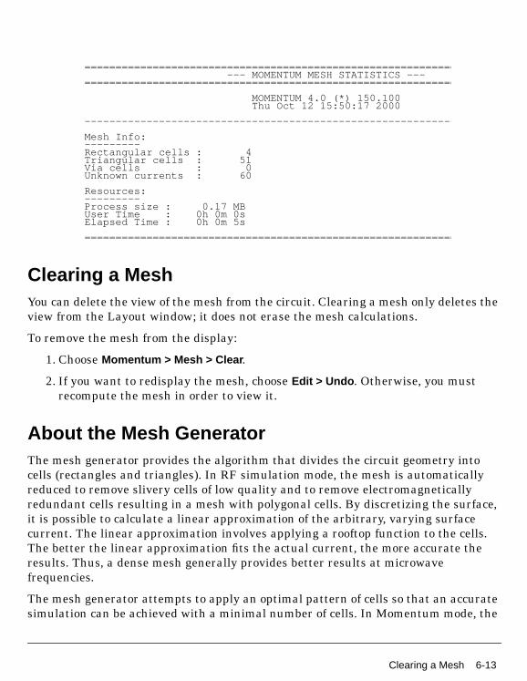
Clearing a Mesh 6-13
Clearing a MeshYou can delete the view of the mesh from the circuit. Clearing a mesh only deletes theview from the Layout window; it does not erase the mesh calculations.
To remove the mesh from the display:
1. Choose Momentum > Mesh > Clear .
2. If you want to redisplay the mesh, choose Edit > Undo . Otherwise, you mustrecompute the mesh in order to view it.
About the Mesh GeneratorThe mesh generator provides the algorithm that divides the circuit geometry intocells (rectangles and triangles). In RF simulation mode, the mesh is automaticallyreduced to remove slivery cells of low quality and to remove electromagneticallyredundant cells resulting in a mesh with polygonal cells. By discretizing the surface,it is possible to calculate a linear approximation of the arbitrary, varying surfacecurrent. The linear approximation involves applying a rooftop function to the cells.The better the linear approximation fits the actual current, the more accurate theresults. Thus, a dense mesh generally provides better results at microwavefrequencies.
The mesh generator attempts to apply an optimal pattern of cells so that an accuratesimulation can be achieved with a minimal number of cells. In Momentum mode, the
=========================================================== = --- MOMENTUM MESH STATISTICS ---=========================================================== =
MOMENTUM 4.0 (*) 150.100 Thu Oct 12 15:50:17 2000
----------------------------------------------------------- -
Mesh Info:---------Rectangular cells : 4Triangular cells : 51Via cells : 0Unknown currents : 60
Resources:---------Process size : 0.17 MBUser Time : 0h 0m 0sElapsed Time : 0h 0m 5s
=========================================================== =

6-14 About the Mesh Generator
Mesh
minimal number of cells can be rather high, resulting in a dense mesh. For a givenmesh density, the mesh reduction technology used in the RF mode achieves anoptimal mesh with significantly fewer cells, hence improving the simulationperformance with reduced memory usage and simulation time. Since the current ineach cell is calculated in a simulation, a very dense mesh can increase simulationtime.
The mesh parameters that you specify provide the mesh maker with the informationrequired to divide your geometry into the various cell shapes and sizes. If you do notwant to set mesh parameters, default ones will be used instead. In Momentum mode,the default mesh setting is 20 cells/wavelength using edge mesh. In RF mode, thedefault mesh setting is 20 cells/wavelength not using edge mesh.
Adjusting Mesh Density
Two mesh parameters, Frequency and Cells per Wavelength, are used in combinationin determining mesh density.
Using the wavelength of the frequency, a linear function is approximated, alsoreferred to as a rooftop basis function. The higher the frequency, the morewavelengths fit across the structure. The Cells per Wavelength are the minimumnumber of cells that fit under each wavelength. The more cells, the better thesinusoid is represented, and the more accurate the simulation is. For example, if youuse 30 cells per wavelength, the maximum deviation between the sinusoid and thelinear approximation is about 1%. These parameters affect longitudinal current.
Higher frequencies will result in a greater number of cells (increased density) for amesh. Similarly, increasing the minimum number of cells per wavelength will alsoincrease the density. In general, for optimal density, it is better to increase thenumber of cells per wavelength rather than increasing the mesh frequency. Theoptimal value for the mesh frequency is the highest frequency that will be simulated.This may avoid having to recalculate the substrate frequency band if it is notsufficient.
If you enter a value for the mesh frequency, but you have already seeded the layout,the system will ignore the frequency you enter and the mesh frequency will only beused to compute the mesh for the remaining areas of the circuit.
You should be aware that the value entered for the number of cells per wavelength isonly a lower limit and not the exact value used by the mesh generator. The followingdiscussion explains how the actual number of cells used by the mesh generator maybe greater. For example, suppose you enter 20 for Cells per Wavelength. In general,

About the Mesh Generator 6-15
the cell size used when the geometry is infinitely large corresponds with the numberof cells per wavelength. But when other details, edges, and user-defined meshsettings are included, cells might appear that are smaller than resulting inmore cells per wavelength than the value of 20 that you entered. Here are two specificcases where the actual number of cells per wavelength is greater:
• When the layout has details that are smaller than , the mesh follows theshape of the details. Since the mesh consists of triangles and rectangles only,the cells will be less than .
• When you change the default settings in the Mesh Setup Controls dialog box,such as the number of cells per transmission line width, then you directlyinfluence the number of cells over the width of the transmission lines. Thismight lead to cells that are smaller than .
About the Edge Mesh
The edge mesh feature automatically creates a relatively dense mesh pattern of smallcells along the edges of metal or slots, and a less dense mesh pattern of a few largecells in all other areas of the geometry. Because most of the current flow occurs alongthe edges of slots or metals, the edge mesh provides an efficient solution with greateraccuracy.
Use the edge mesh to improve simulation accuracy when solving circuits where themodeling of current flow in any edge area is a critical part of the solution. Thisincludes circuits where the characteristic impedance or the propagation constant arecritical for determining the electrical model, circuits in which close proximitycoupling occurs, or circuits where edge currents dominate the circuit behavior.Applications for using the edge mesh include:
• Tightly coupled lines
• Patch antennas
• Resonant circuits
• Delay lines
• Hairpin filters
Edge mesh is available for all levels of meshing: global, layout layer, and objectmeshing.
λ 20⁄
λ 20⁄
λ 20⁄
λ 20⁄

6-16 About the Mesh Generator
Mesh
Setting the Width of the Edge Mesh
When using an edge mesh, you can either specify the edge mesh width or leave itblank. If you leave it blank, an appropriate width will be determined and used tocreate the mesh. One way to get a visual approximation is to position the mouse onthe primitive edge and click, then move the mouse inward and note the differentialvalue., which is displayed at the bottom of the Layout window.
About the Transmission Line Mesh
Use the transmission line mesh when you want to specify the number of cellsbetween parallel lines in a layout. This feature can save computation time andmemory because it will create a mesh that is appropriate for straight line geometry.
For example, the simulation results for a single transmission line with one or twocells across the width will be equal. If you have coupled lines, the results will differ.
Combining the Edge and Transmission Line Meshes
Both transmission line mesh and edge mesh can be used together. The total numberof cells wide will be the total number of transmission line cells plus edge cells. Theminimum value permitted when using this combination is 3.
differential coordinates

About the Mesh Generator 6-17
The edge and transmission line mesh affect the transverse current in the circuit. Themore cells specified using edge mesh and transmission line mesh, the more accuratetransverse current approximations will be.
Basic Edge Mesh
cells/width = 3
Transmission Line Mesh
cells/width = 3
Edge Mesh and Transmission Line Mesh
cells/width = 5
Cell width along the lengthwill be equal for thistype of mesh.

6-18 About the Mesh Generator
Mesh
The plot below illustrates the hairpin example simulated with and without and edgemesh. Although the simulation that includes the edge mesh takes more time, theresults are closer to the actual measured results of the filter.
Mesh Patterns and Simulation Time
The mesh generator is relatively fast, even for complex meshes. But be aware thatthe complexity of the mesh can have a significant on effect simulation time. Inparticular, the number of cells in the mesh (especially triangular cells) and thenumber of unknown currents, can affect simulation time.
Simulation times will be faster when the mesh consists mostly of rectangular cells. Asimple mesh is one consisting of a few rectangles of similar size. A worst-casecomplex mesh would consist of many dissimilar triangles. You should try to minimizethe number of triangular cells in the mesh.
The second variable, number of unknown currents, depends on the density, or totalnumber of cells in the mesh. You should try to minimize the total number of cells inthe mesh. This reduces the number of unknown currents, and thus reduces the size ofthe matrix to be solved during simulation. The amount of time required to solve thematrix is N*N*N, where N is the number of unknown currents.
with edge mesh
withoutedge mesh

About the Mesh Generator 6-19
For example, a thru-line at a global seeding of 30 might produce a 50 x 50 matrix tosolve. Since the time required to solve the matrix is proportional to the matrix size,the same thru-line at a seeding of 60 might produce a 200 x 200 matrix becausenumber of cells would be twice as dense in both X and Y dimensions. This means thatit will take longer to solve.
Adjustments to your mesh parameters can be made to control complexity of the meshand, in turn, the amount of time required to simulate.
For complex circuits, where simulation times may be long even with a simple mesh,reducing the complexity of a mesh can save significant amounts of simulation time.
Mesh Patterns and Memory Requirements
The number of unknown currents, which is calculated when the mesh isprecomputed, is based on the complexity of the mesh. The more unknowns, the largerthe matrix that must be solved during simulation. The amount of memory required tosolve is proportional to N*N, where N is the number of unknown currents.
Using the Arc Facet Angle
The Arc Facet Angle parameter enables you to control the number of triangular cellsthat appear in the mesh. Triangular cells are used to generate a mesh on the curvedarea of an object. The larger the value in the Arc Facet Angle field, the fewer thenumber of triangular segments will be used on the curved object.
The maximum value for the Arc Facet Angle is 45 degrees. The minimum valuedepends on the original facetting used when the curved object was drawn. Forexample, the Double Patch Antenna is drawn with an Arc/Circle Resolution of 30degrees, and the Arc Facet Angle is set to 45 degrees. The actual value used to refacetthe object will be in between these values. The angle is chosen so that the facet lengthis smaller or equal to the cell size, so refacetting will not affect the cells perwavelength that is specified for computing mesh density.
Note In order for the mesh generator to produce an accurate mesh, the mesher mustbe able to recognize the polygon translation it receives as an arc. Therefore, a poorlydefined layout resolution may prevent arc recognition and by that arc refacetting. Formore information on layout resolution, refer to “Mesh Precision and Gap Resolution”on page 6-25.
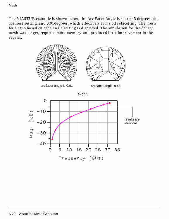
6-20 About the Mesh Generator
Mesh
The VIASTUB example is shown below, the Arc Facet Angle is set to 45 degrees, thecoarsest setting, and 0.01degrees, which effectively turns off refacetting. The meshfor a stub based on each angle setting is displayed. The simulation for the densermesh was longer, required more memory, and produced little improvement in theresults.
arc facet angle is 0.01 arc facet angle is 45
results areidentical

About the Mesh Generator 6-21
Processing Object Overlap
The parameter Thin layer overlap extraction should be used in designs that includethin layers that are both close together and overlapping. It is possible that mesh cellscan be generated that cross the overlap region, and this is not desirable.
As an example, consider two layers, one above the other, and close together. Theycarry a large charge density where they overlap, which increases proportionally to1/distance. If there is no metal above the layers, the charge density is nearly zerowhere there is no overlap, and the change is very rapid—nearly a step—at the pointof overlap.
If no overlap extraction is performed, the mesher can create cells that will cross theborder of the overlap. In the actual circuit, this cell would have a partially highcharge density area where the overlap is present, and a partially low charge densityarea where there is no overlap. However, Momentum simulates cells with a constantcharge density, and approximating the strongly-varying charge in the cell with a
Arc Facet Angle = 45 Arc Facet Angle = 0.01
Process size 6.18 MB 12.791 MB
User time 12 min 20 min
Elapsed time 15 min 24 min
Rectangular cells 96 80
Triangular cells 108 200
Via cells 16 36
Unknown currents 337 453
layer 1
dielectric
cross-section viewof layers
area of overlaphigh charge density
layer 2

6-22 About the Mesh Generator
Mesh
constant is not an adequate representation. Thus, by enabling thin layer extraction,no cells will be created that cross an overlap region.
Because enabling this feature for all possible overlap in a circuit would create toodense a mesh, some empirical rules are implemented that switch the overlapextraction off if the layers are not close (h > 0.02 estimated cell size) or if the overlaparea is small. To calculate the estimated cell size, the mesh frequency, the globalnumber of cells per wavelength, and an estimation of the effective refractive index ofthe substrate are used.
If you are calculating your mesh at low frequencies, the estimated cell size is high,and you may not want thin layer overlap extraction. In this case, disable the Thinlayer overlap function.
Mesh Generator Messages
When a mesh is generated, you may see a message similar to this:
On some layers, the mesher used the maximum allowable cell size for the givensubstrate. You will not be able to generate a coarser mesh on these layers.
This means that the coarsest mesh has been achieved for the objects on certainlayers. This is because the maximum cell size has been limited due to the accuracy ofthe Green’s functions that were calculated for the substrate.
For example, consider a layout with 20-cell mesh when the mesh frequency is 10GHz. Generally, you would get a 10-cell mesh if you set the mesh frequency to 5 GHz.But if, with the lower mesh frequency, the cell size would be larger that the maximum
top views of layer 1
mesh cell crossesinto area of overlap
with overlap extraction,cells are resized, thereis no crossover intoarea of overlap

Guidelines for Meshing 6-23
allowed (the limit being based on the accuracy of the Greens’ function of thesubstrate), the mesh would contain more than 10 cells.
Guidelines for MeshingThe default mesh will provide an adequate and accurate answer for many circuitapplications. For most other circuit applications, the using the global meshparameters will be all that is needed to provide greater accuracy. In a few specialcases, you may need to use the layer or primitive mesh controls.
For applications such as highly accurate discontinuity modeling or for geometriesthat have tightly coupled lines, the default mesh may not be dense enough inparticular areas to provide enough accuracy. In such cases, edge mesh should be usedor the mesh density must be increased. For example, noise floor and dynamic rangeare typically small numbers. In some cases, geometry solutions may show a low valueof S21, like -60 dB, using a dense mesh. Such values are different for a default mesh,which may result in -40 dB for the same circuit.
In any one design, you can use any combination of the four types of mesh control. Ingeneral, greater mesh density can provide more accuracy. But greater density takesmore computation time (more cells to solve) and, additionally, triangles always takelonger to compute than rectangles.
Meshing Thin Layers
Thin layers must be meshed so that the mesh cells are entirely within or entirelyoutside of the overlapping area. If the mesh cells and object boundaries are notaligned correctly, the simulation data may be less accurate.
For more information, refer to “Processing Object Overlap” on page 6-21.
Meshing Thin Lines
When the geometry has narrow lines, like thin transmission paths in a spiral, it maybe difficult to have a mesh that is more than one cell across the width if the defaultglobal mesh is used. If needed, use Edge Mesh or Transmission Line Mesh to capturethe current distribution across the line.

6-24 Guidelines for Meshing
Mesh
Meshing Slots
Slots should be meshed exactly the same as strips—there is no difference. Forexample, the edge mesh can be used for slots because the current distribution isbasically the same, that is, it is concentrated on the edges of a slot.
Adjusting the Mesh Density of Curved Objects
Vias or other curved objects, when drawn in a layout, have a default value for thenumber of facets used to draw the object, based on the command Options >Preferences> Entry/Edit >Arc/Circle Radius (degrees). If the value is small, arelatively large number of facets are used to draw the circle, and this can result inmore triangular cells created the curved areas during the mesh process. To changethe number of facets for all arcs and circles, use the command shown above. Tochange them for a single object, select the object, then choose Edit > Modify >Arc/Circle Resolution. Then increase the number of degrees for the radius, asdesired, to reduce the number of triangles. Be aware that this does alter the geometryof the circuit.
For information on how the mesh parameter Arc Facet Angle affects a mesh, refer to“Using the Arc Facet Angle” on page 6-19.
Discontinuity Modeling
A microstrip transmission line with a bend, using the default mesh, may have a cellsize equal to the width of the line (one cell per line-width). If it is long and the bend isnot severe, then the default mesh may be adequate because the discontinuity isproportionally small compared to the line length. However, if the reference planes aremoved inward or if the bend is more severe, the discontinuity and resulting parasiticsare in greater proportion to the rest of the line. In that case, the default mesh mayresult in simulation data with an error.
To correct this inaccuracy, the mesh should be increased and edge mesh used. Whenthe area near the discontinuity is meshed so that the cell size is equal to a third of theline-width (three cells per line-width) the resulting error is reduced. The denser meshallows for current crowding (parasitic series inductance) at the interior corner of thebend and charge build-up (parasitic shunt capacitance) at the outer edge of the bend.

Guidelines for Meshing 6-25
Solving Tightly Coupled Lines
An example of a tightly coupled line would be a microstrip coupled line filter on a 25mil Alumina substrate (Er = 9.8) where the line width is 25 mils and the separationbetween the lines is 2.5 mils. The filter response is sensitive to coupling between thelines and the default mesh is 1 cells per line-width. In this case, the reflectioncoefficient data does not match measurement data. To solve this design properly, edgemesh must be used.
Editing Object Seeding
The recommended way to seed primitives is to use the o,u,v-coordinate system:
1. Select the object.
2. Choose Momentum > Mesh > Setup .
3. Click Primitive Seed .
4. Click Clear.
5. Select new seed parameters.
It is possible to modify these values by editing the properties of the object. Thismethod is not supported or recommended. Select the object, then choose Edit >Properties. Seed values are displayed and can be changed.
Mesh Precision and Gap Resolution
This section will apply mainly to designs that are imported into Advanced DesignSystem.
Mesh resolution is directly related to the Layout Precision dbu (data base units)value. All gaps or other unresolved layout vertices will be resolved by the meshgenerator if their distance is less than 2 dbu.

6-26 Guidelines for Meshing
Mesh
Use the Layout command Options > Preferences > Layout Units to change the unitsfor your fabrication or layout process as needed.
Gap is 0.1 mil actual.
Mesh recognizes gap becauseprecision is within the dbuunits setting.
Gap is collapsed in the meshbecause the dbu precisionvalue is greater than the gap.
EXAMPLE: Precision dbu set to 0.01mil.
EXAMPLE: Precision dbu set to 1 mil.

7-1
Chapter 7: SimulationThe simulation process combines the Green’s functions that were calculated for thesubstrate of a circuit, plus mesh information that was calculated for the circuit, andsolves for currents in the circuit. Using these current calculations, S-parameters arethen calculated for the circuit.
Prior to running a simulation, the following criteria must be met:
• A substrate definition must be specified for the circuit
• The circuit must include at least one port
• A mesh must be defined for the circuit
• A simulation frequency plan must be specified
If any one of the above criteria is not met, Momentum will report the error if you tryto run a simulation.
The Momentum planar solver uses information from the substrate database and themesh generator to perform the circuit simulation. The substrate calculations andmesh may be computed prior to running the simulation to ensure they are valid. Thiswill reduce simulation time.
The steps for performing a simulation include:
• Specifying and editing frequency plans
• Selecting a process mode
• Specifying solution files
• Electing to view data
• Running the simulation
The steps for each part of this procedure follows.
Note Momentum creates several files under during simulation. One of these files,../mom_dsn/proj_cvi can be large. (This files contains the computed currents.) Afteryou are finished with a particular project, you may want to delete this file to free diskspace.

7-2 Setting Up a Frequency Plan
Simulation
Setting Up a Frequency PlanYou can set up multiple frequency plans for a simulation. For each plan, you canspecify that a solution be found for a single frequency point or over a frequency range.You can also select one of several sweep types for a plan. This collection of frequencyplans will be run as a single simulation.
To set up a frequency plan:
1. Choose Momentum > Simulation > S-parameters .
2. Select a sweep type. The choices are:
• Adaptive
• Logarithmic
• Linear
• Single point
Adaptive is the preferred sweep type. It uses a fast, highly accurate method ofcomparing sampled S-parameter data points to a rational fitting model. Thevalue entered in the Sample Points Limit field is the maximum number ofsamples used in an attempt to achieve convergence. The solutions from the finalattempt will be saved. If convergence is achieved using fewer samples, thesolutions are saved and the simulation will end. For more information aboutthis sweep type, refer to “About Adaptive Frequency Sampling” on page 7-20.
Logarithmic simulates over a frequency range, selecting the frequency points tobe simulated in logarithmic increments. Type the start and the stop frequenciesin the Start and Stop fields, and select frequency units for each. Enter thenumber of frequency points to be simulated per decade of frequency in thePoints/Decade field, and select units.
Linear simulates over a frequency range, selecting the frequency points to besimulated in linear increments based on the step size you specify. Type the startand the stop frequencies in the Start and Stop fields, and select frequency unitsfor each. Enter the step size in the Step field, and select units.
Single simulates at a single frequency point. Type the value in the Frequencyfield and select the units.
3. When you are finished setting the plan, click Add to Frequency Plan List .

Setting Up a Frequency Plan 7-3
Note In a simulation, frequency plans are executed in the order in which theyappear in this list.
4. Repeat these steps to insert additional frequency plans.
5. When you are finished, click Apply .
Considerations
In general, the Adaptive sweep type is the preferred sweep type. The exception iscases where a specific frequency point or points must be simulated, such as the needto view antenna patterns. Since radiation patterns can be calculated only at solvedfrequencies, you may want to specify a single specific frequency using the Singlesweep type, or a range using Linear or Logarithmic sweep types.
If you use one or more sweep types, make sure to set up your frequency plan list sothat plans with Adaptive sweep types are at the top of the list. Any additional plansthat use other sweep types should follow these plans.
Editing Frequency Plans
You can modify, delete, or move frequency plans in the Frequency Plans list.
To modify a frequency plan:
1. Choose Momentum > Simulation > S-parameters .
2. Select the frequency plan from the Frequency Plans list.
3. Edit the plan using the sweep type and frequency fields displayed underEdit/Define Frequency plan. These fields are described in the previous section.
4. When you are finished editing the plan, click Update .
5. Click Apply to save the changes.
To delete a frequency plan:
1. Choose Momentum > Simulation > S-parameters .
2. Select the frequency plan from the Frequency Plans list.
3. Click Cut .

7-4 Selecting a Process Mode
Simulation
4. Click Apply to save the changes.
To move a frequency plan:
1. Choose Momentum > Simulation > S-parameters .
2. Select frequency plan from the Frequency Plans list.
3. Click Cut .
4. Select the frequency plan that you want positioned below the plan that you cut.
5. Click Paste to reenter the plan.
6. Click Apply to save the changes.
Tip You can perform several editing tasks, then click Apply once before you dismissthe dialog box.
Selecting a Process ModeYou can select whether the simulation is to be performed in the foreground or in thebackground. The Foreground mode will pause a simulation if the substrate has notyet been precomputed. In this case, you can choose to stop the simulation or, if youchoose to continue, the substrate will be precomputed and then the simulation will beperformed. The Background mode automatically precomputes the substrate ifnecessary, without prompting you to stop or continue the simulation, then performsthe simulation. In either mode, the Layout window is available to build or editlayouts. For more information on precomputing a substrate, refer to “Precomputingthe Substrate Function” on page 3-18.
To set the process mode:
1. Choose Momentum > Simulation > S-parameters .
2. Select the process mode: choose either Foreground or Background.
3. Click Apply .
Reusing Simulation Data 7-5
Reusing Simulation DataTo reduce the time required to complete the current simulation, you can use sampleddata from the previous simulation. This function is useful if you extend or shift thefrequency plan and resimulate, or if you want more samples near a resonancefrequency. If you change the circuit geometry, substrate, ports, or mesh parameters,simulation data cannot be reused.
Note Momentum does not verify that the design has not changed. Make sure thatonly the frequency plan has changed before attempting to reuse data.
Enabling the function reuses previously calculated S-50 parameters.
To reuse data from the last simulation:
1. Choose Momentum > Simulation > S-parameters .
2. Enable Reuse files from previous simulation if you want to use data from theprevious simulation. Sampled data from the previous simulation will be used inthe current simulation, which can decrease simulation time.
3. Click Apply .
Saving Simulation DataA dataset stores the solutions for one simulation only. If you perform multiplesimulations and want to save the data from previous simulations, you must specify aunique dataset name for each simulation.
One simulation can produce one or two datasets:
• Data at the frequency points computed by the simulator are stored in<project_name>.ds. It is the standard dataset created from any simulation.
• If the Adaptive sweep type is used to simulate, data computed by AFS at eachsampled frequency point is stored in the dataset <project_name>_a.ds.
If you change the name in the Dataset field, the datasets will use the new name andnot the default project_name.
To specify the dataset:
1. Choose Momentum > Simulation > S-parameters .

7-6 Viewing Results Automatically
Simulation
2. The name of the default dataset is displayed in the Dataset field. This is the filein which the simulation data will be stored. The default name is based on thename of the current project.
If you want to use a different dataset, either type the name of a new datasetinto the Dataset field, or click Browse to reuse a dataset. If you choose Browse , alist of the datasets in the data folder of the current project are displayed. Selectfile name and click OK.
Dataset files use the extension .ds and are stored in the data folder of the currentproject.
3. Click Apply to accept the changes.
Saving Data for Export
Momentum simulation data can be saved to a file for use in IC-CAP. Momentumdesign geometry and setup information can be saved for import into Agilent HFSSwithout running a simulation first. For more information, refer to Appendix C,Exporting Momentum Data.
Viewing Results AutomaticallySimulation data is saved in datasets, so you can view simulation results at yourconvenience. If you choose to view results immediately after the simulation iscomplete, enable Open data display when simulation completes. A data displaywindow containing default plot types or the data display template of your choice willbe automatically opened when the simulation is finished. The defaults includemagnitude and phase plots of S-parameters, and S-parameters plotted on Smithcharts.
If you are using the Adaptive sweep type for your simulation, the data from both thestandard and adaptive datasets are displayed for comparison. Data from thestandard dataset will be displayed as discrete points, the adaptive sweep data will bedisplayed as a linear trace.
To open a data display window:
1. Choose Momentum > Simulation > S-parameters .
2. Enable Open data display when simulation completes.

Starting a Simulation 7-7
3. If you want a template to be loaded into the window, type the name of thetemplate in the Template field or click Browse . A list of templates in the datafolder of the current project are displayed. Select a template and click OK.
Note If you want to use a template from another project or location, copy thetemplate into the data folder of the current project.
4. Click Apply to accept the changes.
Starting a SimulationThe simulation process solves for currents by combining the Green’s functions thatwere precomputed for the substrate and the mesh calculations. S-parameters arethen calculated and saved to the dataset.
To start a simulation:
1. Choose Momentum > Simulation > S-parameters .
2. Verify that at least one frequency plan appears in the Frequency Plans list.
3. Check that the Process Mode, Solution Files, and Data Display options are setto your specifications.
4. Click Simulate .
Any messages or errors that occur are displayed in the Momentum Status window. Toindicate progress, a line of dots appears across the Status window if the number ofunknowns in the simulation is greater than 500; otherwise, only the frequencies aredisplayed.
If the simulation fails for a reason related to the setup, the partial data is saved and amessage appears in the Status window.
Viewing Simulation Status
After a simulation is started, any messages regarding the simulation will appear inthe Momentum Status window. Messages usually refer to any errors found, thepercent of completion, and simulation completion.
If you close the status window and want to reopen it, from the Layout menu barchoose Window > Restore Status.

7-8 Stopping a Simulation
Simulation
Understanding the “% Covered” Status Message
This message is generated when running Adaptive sweep types. It indicates thepercentage of the total simulation frequency range that has been accurately modeledby rational functions. When an Adaptive sweep starts, the AFS process attempts torepresent all S-parameters with a number of rational functions. New sample pointsare selected adaptively (by minimizing global error criteria). If the frequency range istoo large, the frequency range will be split into sections. If the fitting model isaccurate and stable within a subrange, the “% covered” message will be updated.Thus, the message indicates the percentage of the total simulation frequency rangethat has been accurately modeled by rational functions.
The AFS process always looks at the whole frequency range and adds samples wherethe fitting errors are maximal (a global error reduction approach). If the fittingconverged in a section of the frequency range, it is likely to converge in the remainingsections, and it will not take many extra samples to achieve full convergence. This iswhy the percent completed message updates very slowly at first, but updates quicklywhen the process is nearly complete.
Stopping a SimulationTo stop a simulation:
1. From the Momentum Status window, choose Simulation/Synthesis > StopSimulation .
The simulation will stop and the partial data will be saved. To reuse the saveddata:
• Choose Momentum > Simulation > S-parameters , enable Reuse files fromprevious simulation , click Apply , then click Simulate .

Viewing the Simulation Summary 7-9
Viewing the Simulation SummaryAs the simulation progresses, you can view substrate, mesh, and solution statistics.Some of the information returned includes time to solve, the resources required, cellinformation, and any messages that were displayed in the status window. Anexample of solution statistics is given next.
Choose Momentum > Simulation > Summary to view the data. Click Refresh toupdate the statistics as the simulation progresses. The following example shows a(partial) summary displayed when using the Momentum microwave simulationmode.

7-10 Viewing the Simulation Summary
Simulation
======================================================================== --- MOMENTUM GENERATION STATISTICS ---======================================================================== Momentum 4.0 (*) 150.999 Tue Jun 12 16:06:24 2001------------------------------------------------------------------------TOTALS------------------------------------------------------------------------
Process size : 2.16 MBUser Time : 0h01m11sElapsed Time : 0h01m13s========================================================================
--- MOMENTUM MESH STATISTICS ---========================================================================
Momentum 4.0 (*) 150.999Tue Jun 12 16:06:24 2001
-----------------------------------------------------------------------Mesh Info:---------Rectangular cells : 148Triangular cells : 2Via cells : 16Unknown currents : 252
Resources:---------Process size : 1.41 MBUser Time : 0h00m00sElapsed Time : 0h00m02s
======================================================================== = --- STATUS SERVER MESSAGES ---
======================================================================== Simulation / Synthesis MessagesMesh will be generated @ 2.000000 GHzStatus / Summary----------- Momentum Simulation --------------Version: Momentum 4.0 (*) 150.999 Dec 13 2000Simulation mode: microwaveDesign: cirstart compute mesh on Tue Jun 12 16:06:16 2001mesh computation successful on Tue Jun 12 16:06:24 2001start simulate circuit on Tue Jun 12 16:06:24 2001start calculate low frequency behavior.simulation frequency = 0.000000 GHzsimulation frequency = 0.109000 GHzsimulation frequency = 0.218000 GHzstart adaptive frequency sweep.simulation frequency = 2.00000 GHzadaptive frequency sweep: 0.0 % of frequency range covered.simulation frequency = 1.33333 GHzsimulation frequency = 0.666667 GHzadaptive frequency sweep: 100.0 % of frequency range covered.circuit simulation successful on Tue Jun 12 16:06:59 2001Writing dataset files...

Viewing the Simulation Summary 7-11
The next example shows a summary from another project using the Momentum RFmode. Notice that it contains information about the matrix size after mesh reductionand the statistics for the quasi-static calculations.

7-12 Viewing the Simulation Summary
Simulation
For examples of substrate and mesh statistics, refer to “Viewing SubstrateComputation Status” on page 3-19, and “Viewing the Mesh Summary” on page 6-12.
=======================================================================------ MOMENTUM SUMMARY ------
Momentum RF 4.0 (*) 150.400Tue Sep 12 13:56:05 2000
-----------------------------------------------------------------------MESH-----------------------------------------------------------------------STATISTICS----------
Rectangular cells : 295Triangular cells : 2451Via cells : 168Edge currents : 3369
RESOURCES---------
Process size : 6.20 MBUser Time : 0h 5m49sElapsed Time : 0h 5m52s
-----------------------------------------------------------------------SOLVER USER TIME ELAPSED TIME MEMORYPROCESSES (h:m:s) (h:m:s) (MB)-----------------------------------------------------------------------SIMULATION SET-UP-----------------
Initialization | 0: 0: 0 | 0: 0: 2 | 2.93Ports analysis | 0: 0: 0 | 0: 0: 0 | 0.53Mesh reduction | 0: 0: 1 | 0: 0: 1 | 5.82Basis creation | 0: 0: 0 | 0: 0: 1 | 6.64Basis unknowns : 783
QUASI-STATIC CALCULATIONS-------------------------
Green functions | 0: 0: 0 | 0: 0: 0 | 0.20Matrix load | 0:15:56 | 0:15:58 | 9.82
1. SIMULATION FREQUENCY = 0 Hz-------------------------
Matrix load | 0: 0: 0 | 0: 0: 0 | 6.19Matrix solve | 0: 0:13 | 0: 0: 0 | 0.03S parameters | 0: 0: 8 | 0: 0: 8 | 7.35

Performing Remote Simulations 7-13
Performing Remote SimulationsMomentum can require significant computer resources in order to perform asimulation. Depending on your needs, it might be advantageous to install a relativelypowerful computer with a large amount of RAM, and dedicate it for runningsimulations only, while using less powerful workstations for other tasks. With such asetup, you can perform design and setup procedures from a local, less powerfulworkstation, while the simulations, which require the bulk of thecomputation-intensive operations, are sent off to the (remote) computer that you havededicated for running simulations.
Note Refer to the installation guides for instructions on performing remotesimulations with other simulators.
Momentum is designed to support remote operation. You can perform remotesimulations using these hardware configurations:
• UNIX to UNIX
• PC to PC
The steps to perform remote simulations with these configurations are below.
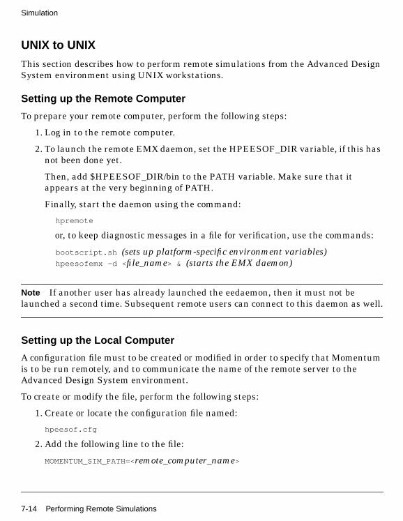
7-14 Performing Remote Simulations
Simulation
UNIX to UNIX
This section describes how to perform remote simulations from the Advanced DesignSystem environment using UNIX workstations.
Setting up the Remote Computer
To prepare your remote computer, perform the following steps:
1. Log in to the remote computer.
2. To launch the remote EMX daemon, set the HPEESOF_DIR variable, if this hasnot been done yet.
Then, add $HPEESOF_DIR/bin to the PATH variable. Make sure that itappears at the very beginning of PATH.
Finally, start the daemon using the command:
hpremote
or, to keep diagnostic messages in a file for verification, use the commands:
bootscript.sh (sets up platform-specific environment variables)hpeesofemx -d < file_name> & (starts the EMX daemon)
Note If another user has already launched the eedaemon, then it must not belaunched a second time. Subsequent remote users can connect to this daemon as well.
Setting up the Local Computer
A configuration file must to be created or modified in order to specify that Momentumis to be run remotely, and to communicate the name of the remote server to theAdvanced Design System environment.
To create or modify the file, perform the following steps:
1. Create or locate the configuration file named:
hpeesof.cfg
2. Add the following line to the file:
MOMENTUM_SIM_PATH=<remote_computer_name>

Performing Remote Simulations 7-15
3. Place the file in one of four directories, which are searched in the followingorder:
• The current working directory, where Advanced Design System has beenlaunched;
• $HOME/hpeesof/config (most used by individual users);
• $HPEESOF_DIR/custom/config (sets Momentum in remote mode for thewhole site);
• $HPEESOF_DIR/config (the preinstalled configuration, valid for the wholesite);
4. Start Advanced Design System by typing:
hpads
Running the Simulation
Starting a remote Momentum simulation is no different than starting a local one.The same menu selections apply:
• Momentum > Substrate > Precompute
• Momentum > Mesh > Precompute
• Momentum > Simulation > S-parameters
• Momentum > Post-Processing > Radiation Pattern
There are some differences between local and remote simulations in the use of files,though. A local Momentum simulation is usually carried out in a temporarydirectory; remote Momentum simulations are calculated in another directory. Thetemporary directory is guaranteed to have a unique name by a call to a utilitytmpnam, but is always placed under /usr/tmp or /var/tmp. Both of these directoriescan only be accessed by a remote server in very tightly coupled clusters. This is anunnecessary severe restriction. Therefore, the remote computations write theirresults under the local $HOME/mom_tmp/<temporary_name>.

7-16 Performing Remote Simulations
Simulation
Ending Remote Operation
To end a remote simulation setup:
1. On the local machine, exit Advanced Design System.
2. Undo the modification made to the hpeesof.cfg file.
3. Kill the hpeesofemx daemon that is running on the remote server.
4. Log out from the remote server.
The next time Advanced Design System is launched, it will operate Momentumlocally again.
Restrictions
Be aware that the following restrictions apply to remote simulation:
The $HOME/mom_tmp/<temporary_name> directory has wide access permissions(0777).
The $HOME directory, which resides on the local file system, must be visible underthe same path from the remote server (through NFS).
If a substrate computation is required, the user must set access permissions on$HOME/substrates to 0777, and the permissions of the files under it to 0666.However, if the user forgets to do so, the UI will test for it, and it will warn the userthat this must be done.
Under ADS 1.3 and later, remote Momentum simulation behaves exactly the sameway as under Series IV 6.1 release 305.
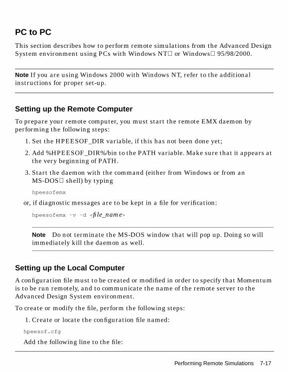
Performing Remote Simulations 7-17
PC to PC
This section describes how to perform remote simulations from the Advanced DesignSystem environment using PCs with Windows NT or Windows 95/98/2000.
Note If you are using Windows 2000 with Windows NT, refer to the additionalinstructions for proper set-up.
Setting up the Remote Computer
To prepare your remote computer, you must start the remote EMX daemon byperforming the following steps:
1. Set the HPEESOF_DIR variable, if this has not been done yet;
2. Add %HPEESOF_DIR%/bin to the PATH variable. Make sure that it appears atthe very beginning of PATH.
3. Start the daemon with the command (either from Windows or from anMS-DOS shell) by typing
hpeesofemx
or, if diagnostic messages are to be kept in a file for verification:
hpeesofemx -v -d < file_name>
Note Do not terminate the MS-DOS window that will pop up. Doing so willimmediately kill the daemon as well.
Setting up the Local Computer
A configuration file must to be created or modified in order to specify that Momentumis to be run remotely, and to communicate the name of the remote server to theAdvanced Design System environment.
To create or modify the file, perform the following steps:
1. Create or locate the configuration file named:
hpeesof.cfg
Add the following line to the file:

7-18 Performing Remote Simulations
Simulation
MOMENTUM_SIM_PATH=<remote_computer_name>
2. Place the file in one of four directories, which are searched in the followingorder:
• The current working directory, where Advanced Design System has beenlaunched
• %HOME%\hpeesof\config (most used by individual users)
• %HPEESOF_DIR%\custom\config (sets Momentum in remote mode for thewhole site)
• %HPEESOF_DIR%\config (the preinstalled configuration, valid for thewhole site)
3. Start Advanced Design System by typing:
hpads
Note It is possible to perform a remote simulation on an NT machine from aWindows 95/98 computer and vice versa.
On NT and Windows 95/98 machines it is possible for two local users to link to thesame remote server.
If using Windows NT machines with Windows 2000 machines, following theadditional steps, “Additional Set-up for Using Windows NT with Windows 2000” onpage 7-18.
Additional Set-up for Using Windows NT with Windows 2000
If you are using Windows NT (local) with Windows 2000 (remote), perform theseadditional steps:
Windows NT (Local)
1. Set your HOME directory to a shared directory (e.g. x:\users\yourName).
2. Make sure HOME is set in the control panel and in the registry(key HKEY_LOCAL_MACHINE\SOFTWARE\AGILENT\ADS\1.7\eeenv\HOME).
3. Start ADS to create $HOME/config and exit.

Performing Remote Simulations 7-19
4. Set EEDAEMON_SOCKET=1801 in $HOME/hpeesof/config/hpeesof.cfg
5. Set MOMENTUM_SIM_PATH=w2k_server_name in$HOME/hpeesof/config/hpeesof.cfg
6. Make sure the directory substrates exists under $HOME
7. Restart ADS and check that EEDAEMON_SOCKET is set equal to 1801
Windows 2000 (Remote)
1. Login with your NT login name (same login on client and server)
2. Set HOME equal to the shared directory (e.g. x:\users\yourName).
3. Make sure this directory is accessible.
4. Make sure HOME is set in the registry and in the control panel.
5. Make sure HOME and HPEESOF_DIR are defined as system variables, not asuser variables.
6. Start hpeesofemx and check that EEDAEMON_SOCKET is set equal to 1801.
Note When launching Momentum, ignore the "Warning #21" messages. They indicatethat the remote process cannot chdir to the starting directory.
Your project can be located on the client side or on the shared drive (x).
Running the Simulation
Launching Momentum simulations is no different than launching local ones. Thesame menu commands apply:
• Momentum > Substrate > Precompute
• Momentum > Mesh > Precompute
• Momentum > Simulation > S-parameters
• Momentum > Post-Processing > Radiation Pattern
There are some differences between local and remote simulations in the use of files,though. A local Momentum simulation is usually carried out in a temporarydirectory; remote Momentum simulations are calculated in another directory. Thetemporary directory is guaranteed to have a unique name by a call to a utility

7-20 About Adaptive Frequency Sampling
Simulation
tmpnam, but is always placed under \temp. As on UNIX, the remote computationswrite their results under the local %HOME%\mom_tmp\<temporary_name>.
Ending Remote Operation
To end a remote simulation setup:
1. On the local machine, exit Advanced Design System.
2. Undo the modification made to the hpeesof.cfg file.
3. Kill the hpeesofemx daemon that is running on the remote server.
The next time Advanced Design System is launched, it will operate Momentumlocally again.
Restrictions
Be aware that the following restrictions apply to remote simulation:
• The $HOME directory, which resides on the local file system, must be visibleunder the same path from the remote server. The restriction here is that thewhole drive must be shared among the PCs.
• If a substrate computation is required, the user must set the$HOME\substrates directory and the files under it accessible for reading andwriting. However, if the user forgets to do so, the UI will test for it, and it willwarn the user that this must be done.
About Adaptive Frequency SamplingAdaptive Frequency Sampling (AFS) is a method of comparing sampled S-parameterdata points to a rational fitting model. In order to accurately represent the spectralresponse of the circuit, the AFS feature in Momentum takes a minimal number offrequency samples and then applies its algorithm to the sampled data. Wherever theS-parameters vary the most, more samples are taken. When the fitting model and thesampled data converge, the AFS algorithm is then complete and the S-parameterdata is written into the dataset. In this way, the maximum amount of information canbe obtained from the minimum amount of sampling.
By using the AFS feature, you can greatly reduce the amount of time required tosimulate circuits that have resonances or other sharp responses that are difficult to

About Adaptive Frequency Sampling 7-21
detect. Data that would have remained hidden using other types of analyses can nowbe obtained.
Even in the case of a low-pass filter, AFS can solve for the S-parameters faster andmore accurately than discrete data sampling. For example, if you were measuring a2 GHz low-pass filter, you would enable the AFS feature and then enter a startfrequency of 500 MHz and a stop frequency of 4 GHz. AFS would then sample the twoend points, construct the fitting model, and then sample points in between as needed.As this occurs, the model is automatically refined and appropriate sample points aretaken until the model and the sampled data converge. When convergence is reached,both sampled data and the AFS data are written into two separate datasets and canbe presented as S-parameter traces on a plot. If the max sample size is reached beforeconverging, the partial results will be saved and can be reused by simulating thecircuit again.
Note AFS data must converge in order to be accurate. Be sure the data is convergedby checking the message in the Momentum Status window. If data is not converged,you will see inaccurate results.
AFS Convergence
Convergence is determined by how close the fitting model is to the sampled data.Convergence is achieved when the sampled points are accurate to -75 dB, and theoverall accuracy is -60 dB.
When AFS is used, be sure that the sampled data has converged with the fittingmodel. This can be checked by the messages in the status window. If converged, themessage will be that AFS is complete. If not converged, a warning will appear.Examples of such warning messages are:
Maximum number of adaptive frequency samples reached!
Fitting models not (completely) converged.
Consider:- increasing maximum number of sample points.
- activating the reuse option.
If you encounter errors, try decreasing the frequency range of the frequency plan andincreasing the number of sample points. Theoretically, some circuits may requireseveral dozen points to converge if they are electrically long. This is because the AFS
7-22 About Adaptive Frequency Sampling
Simulation
program samples the data at about each 60 degree rotation, in the Smith chart, of theS-parameter with the most phase variation.
Note If you simulation does not converge, to help you assess the quality of thesimulation, you can view convergence results in the Data Display. For moreinformation, refer to “Viewing Convergence Data” on page 9-5.
Setting Sample Points
If you are using the Adaptive sweep type in a simulation, you may want to selectspecific sample points to be used in the AFS process. In general, this is not necessary(and is in fact, discouraged), but there may be instances where it is beneficial. Anapplication where this may be beneficial is simulating a structure that has a distinctvariation in response at some point over a frequency range, such as a resonantstructure. To set up the simulation:
1. Select the Single sweep type, enter either the value of the resonant frequency ora value near it in the Frequency field, and add this to the frequency plan list.
2. Select the Adaptive sweep type, set up the plan, then add it to the list offrequency plans.
For this situation, the sample point aids the AFS process by identifying an areawhere there is clearly a variation in the response of the circuit.
Applying extra sample points may be necessary for visualization or far-fieldcalculations.
It is not beneficial to attempt to add sample points for other purposes, such asattempting to force smoothing to occur at specific points, without taking intoconsideration the response at these points. For example:
1. Selecting the Linear sweep type, adding sample points spread linearly acrossthe frequency range, and adding the frequency plan to the list.
2. Adding an Adaptive sweep type, selecting the same frequency range, andadding it to the list.
For this situation, the sample points from the linear simulation will be included inthe adaptive simulation. This impedes the AFS process of selecting the optimaldistribution of samples over the frequency range, and this can produce poorsimulation results.

About Adaptive Frequency Sampling 7-23
To remedy this situation, either run the Adaptive sweep plan first or make sure thatthe frequency ranges of the two plans do not overlap.
Viewing AFS S-parameters
When viewing the S-parameters in an AFS dataset, if you zoom in you may see small,unexpected spurious ripples or oscillations, with an amplitude less than 0.0002. Theamplitude of these oscillations is always less than the AFS accuracy level, which isapproximately -60 dB. Generally, these ripples will only appear if the dynamicbehavior of the S-parameters is limited, for example, an S-parameter that is nearly 1over the frequency range simulated. This is likely due to the rational fitting modelhave too many degrees of freedom and being too complex for this situation.

7-24 About Adaptive Frequency Sampling
Simulation

About Radiation Patterns 8-1
Chapter 8: Radiation Patterns and AntennaCharacteristicsThis chapter describes how to calculate the radiation fields. It also provides generalinformation about the antenna characteristics that can be derived based on theradiation fields. In Momentum RF mode, radiation patterns and antennacharacteristics are not available.
About Radiation PatternsOnce the currents on the circuit are known, the electromagnetic fields can becomputed. They can be expressed in the spherical coordinate system attached to yourcircuit as shown in Figure 8-1. The electric and magnetic fields contain terms thatvary as 1/r, 1/r2 etc. It can be shown that the terms that vary as 1/r2, 1/r3, ... areassociated with the energy storage around the circuit. They are called the reactivefield or near-field components. The terms having a 1/r dependence become dominantat large distances and represent the power radiated by the circuit. Those are calledthe far-field components (Eff, Hff).
Note In the direction parallel to the substrate (theta = 90 degrees), parallel platemodes or surface wave modes, that vary as 1/sqrt(r), may be present, too. Althoughthey will dominate in this direction, and account for a part of the power emitted bythe circuit, they are not considered to be part of the far-fields.
The radiated power is a function of the angular position and the radial distance fromthe circuit. The variation of power density with angular position is determined by thetype and design of the circuit. It can be graphically represented as a radiationpattern.
E r ∞ θ ϕ, ,→( ) Eff θ ϕ,( )e jkr–
r------------=
H r ∞ θ ϕ, ,→( ) H ff θ ϕ,( )e jkr–
r------------=

8-2 About Antenna Characteristics
Radiation Patterns and Antenna Characteristics
The far-fields can only be computed at those frequencies that were calculated duringa simulation. The far-fields will be computed for a specific frequency and for a specificexcitation state. They will be computed in all directions (theta, phi) in the open halfspace above and/or below the circuit. Besides the far-fields, derived radiation patternquantities such as gain, directivity, axial ratio, etc. are computed.
Note It is possible to calculate far-fields for some designs that have a top or bottomlayer that is not defined as open space. For more information on these structures,refer to “377 Ohm Terminations and Radiation Patterns” on page 3-26.
About Antenna CharacteristicsBased on the radiation fields, polarization and other antenna characteristics such asgain, directivity, and radiated power can be derived.
Polarization
The far-field can be decomposed in several ways. You can work with the basicdecomposition in ( , ). However, with linear polarized antennas, it is sometimesmore convenient to decompose the far-fields into (Eco, Ecross) which is a decompositionbased on an antenna measurement set-up. For circular polarized antennas, adecomposition into left and right hand polarized field components (Elhp, Erhp) is mostappropriate. Below you can find how the different components are related to eachother.
is the characteristic impedance of the open half sphere under consideration.
Eθ Eϕ
Eff θ ϕ,( ) Eθ θ ϕ,( )iθ Eϕ θ ϕ,( )iϕ+ Eco θ ϕ,( )ico Ecross θ ϕ,( )icross+ Elhp θ ϕ,( )ilhp Erhp θ ϕ,( )irhp+= = =
HϕEθZw-------=
HθEϕZw-------–=
Zωµε---=
Zω
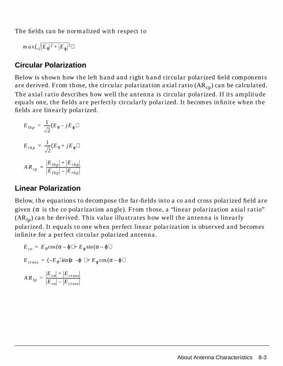
About Antenna Characteristics 8-3
The fields can be normalized with respect to
Circular Polarization
Below is shown how the left hand and right hand circular polarized field componentsare derived. From those, the circular polarization axial ratio (ARcp) can be calculated.The axial ratio describes how well the antenna is circular polarized. If its amplitudeequals one, the fields are perfectly circularly polarized. It becomes infinite when thefields are linearly polarized.
Linear Polarization
Below, the equations to decompose the far-fields into a co and cross polarized field aregiven ( is the co polarization angle). From those, a “linear polarization axial ratio”(ARlp) can be derived. This value illustrates how well the antenna is linearlypolarized. It equals to one when perfect linear polarization is observed and becomesinfinite for a perfect circular polarized antenna.
max Eθ2 Eϕ
2+( )
Elhp1
2------- Eθ jEϕ–( )=
Erhp1
2------- Eθ jEϕ+( )=
ARcpElhp Erhp+
Elhp Erhp–-------------------------------------=
α
Eco Eθ α ϕ–( ) Eϕ α ϕ–( )sin+cos=
Ecross Eθ–( ) α ϕ–( ) Eϕ α ϕ–( )cos+sin=
ARlpEco Ecross+
Eco Ecross–-------------------------------------=

8-4 About Antenna Characteristics
Radiation Patterns and Antenna Characteristics
Figure 8-1. Co polarization angle
Radiation Intensity
The radiation intensity in a certain direction, in watts per steradian, is given by:
For a certain direction, the radiation intensity will be maximal and equals:
Radiated Power
The total power radiated by the antenna, in Watts, is represented by:
Effective Angle
This parameter is the solid angle through which all power emanating from theantenna would flow if the maximum radiation intensity is constant for all angles overthe beam area. It is measured in steradians and is represented by:
U θ ϕ,( ) 12---= Eff θ ϕ,( ) H ff∗× θ ϕ,( )( ) 1
2Zw----------- Eθ θ ϕ,( ) 2 Eϕ θ ϕ,( ) 2+( )=
Umax maxθφ
U θ φ,( )( )=
Prad U θ ϕ,( ) dΩ⋅Ω∫12--- Eff H ff∗ dΩ⋅×Ω∫= =
ΩAPrad
Umax--------------=

About Antenna Characteristics 8-5
Directivity
Directivity is dimensionless and is represented by:
The maximum directivity is given by:
Gain
The gain of the antenna is represented by:
where Pinj is the real power, in watts, injected into the circuit.
The maximum gain is given by:
Efficiency
The efficiency is given by:
Effective Area
The effective area, in square meters, of the antenna circuit is given by:
D θ ϕ,( ) 4πU θ ϕ,( )Prad
--------------------=
D 4πUmax
Prad-------------- 4π
ΩA--------= =
G θ ϕ,( ) 4πU θ ϕ,( )Pinj
--------------------=
G 4πUmax
Pinj--------------=
ηPrad
Pinj------------ G
D----= =
Aeff θ ϕ,( ) λ2
4π------G θ ϕ,( )=
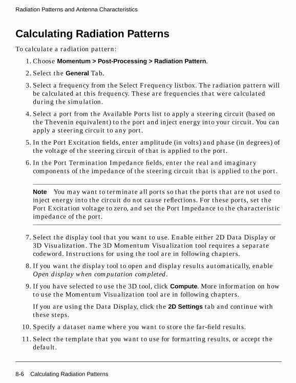
8-6 Calculating Radiation Patterns
Radiation Patterns and Antenna Characteristics
Calculating Radiation PatternsTo calculate a radiation pattern:
1. Choose Momentum > Post-Processing > Radiation Pattern .
2. Select the General Tab.
3. Select a frequency from the Select Frequency listbox. The radiation pattern willbe calculated at this frequency. These are frequencies that were calculatedduring the simulation.
4. Select a port from the Available Ports list to apply a steering circuit (based onthe Thevenin equivalent) to the port and inject energy into your circuit. You canapply a steering circuit to any port.
5. In the Port Excitation fields, enter amplitude (in volts) and phase (in degrees) ofthe voltage of the steering circuit of that is applied to the port.
6. In the Port Termination Impedance fields, enter the real and imaginarycomponents of the impedance of the steering circuit that is applied to the port.
Note You may want to terminate all ports so that the ports that are not used toinject energy into the circuit do not cause reflections. For these ports, set thePort Excitation voltage to zero, and set the Port Impedance to the characteristicimpedance of the port.
7. Select the display tool that you want to use. Enable either 2D Data Display or3D Visualization. The 3D Momentum Visualization tool requires a separatecodeword. Instructions for using the tool are in following chapters.
8. If you want the display tool to open and display results automatically, enableOpen display when computation completed.
9. If you have selected to use the 3D tool, click Compute . More information on howto use the Momentum Visualization tool are in following chapters.
If you are using the Data Display, click the 2D Settings tab and continue withthese steps.
10. Specify a dataset name where you want to store the far-field results.
11. Select the template that you want to use for formatting results, or accept thedefault.

Calculating Radiation Patterns 8-7
12. Select either the planar or conical Cut Type Definition:
• A planar cut is perpendicular to the circuit layout plane.
• A conical cut is a cone around the z-axis.
Refer to the diagram in the Radiation Pattern Control dialog box. For moreinformation, refer to “Planar (Vertical) Cut” on page 8-8 and “Conical Cut” onpage 8-8.
13. Enter the value of the cutting angle, in degrees, in the Cutting Angle field.
• For a planar cut, this angle, phi, is relative to the x-axis. Phi will be keptconstant while theta will be swept from -180 to 180 degrees.
• For a conical cut, the cutting angle, theta, is relative to the z-axis. Theta willbe kept constant while phi will be swept from 0 to 360 degrees.
14. Enter the value of the co polarization angle in the Co Polarization Angle field.This angle will be used when decomposing the far-fields into a co and crosspolar component (see “Linear Polarization” on page 8-3).
15. Enter the threshold for displaying data in the Lower Clipping Boundary field.Select units of dB or mag. Computed radiation pattern data that is below thisvalue will be displayed as zero (when units are mag) or the lower clippingboundary (when units are dB).
16. Click Compute to compute the radiation pattern. After computation, thefar-fields and derived antenna parameters will be stored in a dataset with thename you specified. An _f will be appended to the dataset name. The _findicates that the dataset contains radiation pattern data. The dataset is storedin the /data directory of the current project.
After the radiation calculations are performed, data is saved depending on thedisplay tool selected above:
• 2D Data Display was selected: all data is stored in a single dataset with thename you specified with _f.ds appended. The _f indicates that the datasetcontains radiation pattern data. The dataset is stored in the /data directory ofthe current project.
• 3D Visualization was selected: the far-fields and derived antenna parameterswill be stored in respectively proj.fff and proj.ant in themom_dsn/<design_name> directory of your project.

专注于微波、射频、天线设计人才的培养 易迪拓培训 网址:http://www.edatop.com
A D S 视 频 培 训 课 程 推 荐
ADS–Advanced Design System 是由原美国安捷伦科技(现更名为是德科技)推出的微波射频电路、
通信系统和 MMIC/RFIC 仿真设计软件,其功能强大、应用广泛,被国内高校、科研院所和大型科技
公司使用广为使用。掌握 ADS 无疑能提升相关设计领域工程师的技术实力、提高工作效率。
为了帮助工程技术人员更好、更快的学习掌握 ADS 的使用,易迪拓培训(www.edatop.com)特聘多
年 ADS 使用经验的资深专家精心制作推出了多套 ADS 视频培训课程,由浅入深、全面系统地讲授了
ADS 在微波射频电路设计、通信系统设计和电磁仿真设计方面的仿真设计和应用操作。其中,视频课
程多以设计实例边操作边讲解,工程实践强,且直观易学,能够帮助您在最短的时间内学会使用 ADS,
并把 ADS 真正应用到设计研发工作中去...
ADS 学习培训课程套装
该套装是易迪拓培训和微波 EDA 网联合推出的迄今为止国内最全面、最
权威的 ADS 培训教程,共包含 10 门 ADS 学习培训课程。课程是由具有
多年 ADS 使用经验的微波射频与通信系统设计领域资深专家讲解,并多
结合设计实例,由浅入深、详细而又全面地讲解了 ADS 在微波射频电路
设计、通信系统设计和电磁仿真设计方面的内容。能让您在最短的时间
内学会使用 ADS,迅速提升个人技术能力,把 ADS 真正应用到实际研发
工作中去,成为 ADS 设计专家...
课程网址: http://www.edatop.com/peixun/ads/13.html
更多 ADS 视频培训课程:
两周学会 ADS — 中文视频培训教程
最新版 ADS 的入门和进阶培训课程,适合 ADS2011 ~ ADS2014 以及更新版本 ADS 的学习。是
ADS 初学者的最佳课程,网址:http://www.edatop.com/peixun/ads/14.html
ADS 射频模拟电路设计详解 — 中文视频教程
本课程基于新版的 ADS 软件,由李明洋老师讲授,讲解了 ADS 在微波射频模拟电路设计中的具
体应用,视频课程,直观易学,网址:http://www.edatop.com/peixun/ads/15.html
ADS 高低阻抗线微带滤波器设计(ADS2014 版)— 中文视频教程
该门课程旨在帮助学员快速、全面、透彻地理解高低阻抗线微带滤波器的设计原理和设计步骤,
帮助学员学会并掌握使用 ADS 软件仿真分析和优化设计微带线滤波器的实际操作;课程网址:
http://www.edatop.com/peixun/filter/128.html
更多 ADS 培训课程,敬请浏览:http://www.edatop.com/peixun/ads

`
专注于微波、射频、天线设计人才的培养 易迪拓培训 网址:http://www.edatop.com
关于易迪拓培训:
易迪拓培训(www.edatop.com)由数名来自于研发第一线的资深工程师发起成立,一直致力和专注
于微波、射频、天线设计研发人才的培养;后于 2006 年整合合并微波 EDA 网(www.mweda.com),
现已发展成为国内最大的微波射频和天线设计人才培养基地,成功推出多套微波射频以及天线设计相
关培训课程和 ADS、HFSS 等专业软件使用培训课程,广受客户好评;并先后与人民邮电出版社、电
子工业出版社合作出版了多本专业图书,帮助数万名工程师提升了专业技术能力。客户遍布中兴通讯、
研通高频、埃威航电、国人通信等多家国内知名公司,以及台湾工业技术研究院、永业科技、全一电
子等多家台湾地区企业。
我们的课程优势:
※ 成立于 2004 年,10 多年丰富的行业经验
※ 一直专注于微波射频和天线设计工程师的培养,更了解该行业对人才的要求
※ 视频课程、既能达到现场培训的效果,又能免除您舟车劳顿的辛苦,学习工作两不误
※ 经验丰富的一线资深工程师讲授,结合实际工程案例,直观、实用、易学
联系我们:
※ 易迪拓培训官网:http://www.edatop.com
※ 微波 EDA 网:http://www.mweda.com
※ 官方淘宝店:http://shop36920890.taobao.com
专注于微波、射频、天线设计人才的培养
官方网址:http://www.edatop.com 易迪拓培训 淘宝网店:http://shop36920890.taobao.com