(Advanced) Computer Organization & Architechture Prof. · PDF file(Advanced) Computer...
55
+ (Advanced) Computer Organization & Architechture Prof. Dr. Hasan Hüseyin BALIK (1 st Week)
Transcript of (Advanced) Computer Organization & Architechture Prof. · PDF file(Advanced) Computer...

+
(Advanced) Computer Organization & Architechture
Prof. Dr. Hasan Hüseyin BALIK
(1st Week)

+Outline
• Course Information and Policies
• Course Syllabus
• 1. Overview
—Basic Concepts and Computer Evolution
—Performance Issues

+
Course Information
Instructor: Prof. Dr. Hasan H. BALIK, [email protected], and
www.hasanbalik.com
Class Homepage:
http://www.hasanbalik.com/LectureNotes/CompOrg/
Book: Computer Organization and Architecture, 10th Edition, William Stallings, Prentice Hall 2016
Grading: Assingment (Project) 50% and Final 50%

+
Course Syllabus-1
Overview
Basic Concepts and Computer Evolution
Performance Issues
The computer system
A Top-Level View of Computer Function and
Interconnection
Cache Memory
Internal Memory Technology
External Memory
Input/Output

+Course Syllabus-2
The central processing unit
Instruction Sets: Characteristics and Functions
Instruction Sets: Addressing Modes and Formats
Processor Structure and Function
Reduced Instruction Set Computers (RISCs)
Instruction-Level Parallelism and Superscalar
Processors
Parallel organization
Parallel Processing
Multicore Computers
Control Unit
Control Unit Operation
Microprogrammed Control

+
Outline
1. Overview
1.1 Basic Concepts and Computer Evolution
1.2 Performance Issues

+
1.1 Basic Concepts and
Computer Evolution

Computer Architecture
•The operational units and their interconnections that realize the architectural specifications
•Hardware details transparent to the programmer, control signals, interfaces between the computer and peripherals, memory technology used
• Instruction set, number of bits used to represent various data types, I/O mechanisms, techniques for addressing memory
•Attributes of a system visible to the programmer
•Have a direct impact on the logical execution of a program
Computer Architecture
Architectural attributes include:
Computer Organization
Organizational attributes include:
Computer Organization
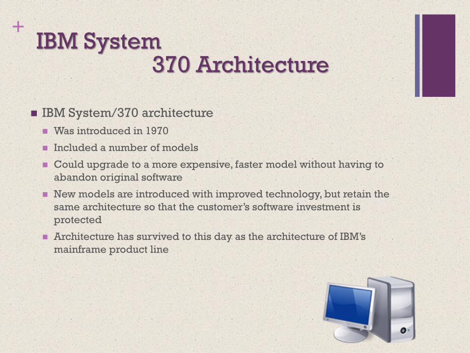
+IBM System
IBM System/370 architecture
Was introduced in 1970
Included a number of models
Could upgrade to a more expensive, faster model without having to
abandon original software
New models are introduced with improved technology, but retain the
same architecture so that the customer’s software investment is
protected
Architecture has survived to this day as the architecture of IBM’s
mainframe product line
370 Architecture

+Structure and Function
Hierarchical system
Set of interrelated
subsystems
Hierarchical nature of complex
systems is essential to both
their design and their
description
Designer need only deal with
a particular level of the system
at a time
Concerned with structure
and function at each level
Structure
The way in which
components relate to each
other
Function
The operation of individual
components as part of the
structure

+Function
There are four basic functions that a computer can perform:
Data processing
Data may take a wide variety of forms and the range of processing requirements is broad
Data storage
Short-term
Long-term
Data movement
Input-output (I/O) - when data are received from or delivered to a device (peripheral) that is directly connected to the computer
Data communications – when data are moved over longer distances, to or from a remote device
Control
A control unit manages the computer’s resources and orchestrates the performance of its functional parts in response to instructions

Structure
Figure 1.1 A Top-Down View of a Computer
Main
memoryI/O
CPU
COMPUTER
System
Bus
ALURegisters
Control
Unit
CPU
Internal
Bus
Control Unit
Registers and
Decoders
CONTROL
UNIT
Sequencing
Logic
Control
Memory

+CPU – controls the operation of
the computer and performs its
data processing functions
Main Memory – stores data
I/O – moves data between the
computer and its external
environment
System Interconnection –
some mechanism that provides
for communication among CPU,
main memory, and I/O
There are four
main structural
components
of the computer:

+CPU
Control Unit
Controls the operation of the CPU
and hence the computer
Arithmetic and Logic Unit (ALU)
Performs the computer’s data
processing function
Registers
Provide storage internal to the CPU
CPU Interconnection
Some mechanism that provides for
communication among the control
unit, ALU, and registers
Major structural
components:

+Multicore Computer Structure
Central processing unit (CPU)
Portion of the computer that fetches and executes instructions
Consists of an ALU, a control unit, and registers
Referred to as a processor in a system with a single processing unit
Core
An individual processing unit on a processor chip
May be equivalent in functionality to a CPU on a single-CPU system
Specialized processing units are also referred to as cores
Processor
A physical piece of silicon containing one or more cores
Is the computer component that interprets and executes instructions
Referred to as a multicore processor if it contains multiple cores

+Cache Memory
Multiple layers of memory between the processor and main
memory
Is smaller and faster than main memory
Used to speed up memory access by placing in the cache
data from main memory that is likely to be used in the near
future
A greater performance improvement may be obtained by
using multiple levels of cache, with level 1 (L1) closest to the
core and additional levels (L2, L3, etc.) progressively farther
from the core

Figure 1.2 Simplified View of Major Elements of a Multicore Computer
MOTHERBOARD
PROCESSOR CHIP
CORE
Processor
chip
Main memory chips
I/O chips
Core
L3 cache
Instruction
logic
L1 I-cache
L2 instruction
cache
L2 data
cache
L1 data cache
Arithmeticand logic
unit (ALU)
Load/
store logic
L3 cache
Core Core Core
Core Core Core Core

+
Motherboard with Two Intel Quad-Core Xeon Processors

IBM zEnterprise EC12
Processor Unit (PU)
Chip Diagram• This chip has 2.75 billion transistors.
• This chip has six cores, or processors
• There are two large areas labeled L3 cache,
which are shared by all six processors.

zEnterprise
EC12
Core Layout
ISU (instruction sequence unit)
IFU (instruction fetch unit)
IDU (instruction decode unit)
LSU (load-store unit): Contains L1
and L2 Cashe
XU (translation unit):
FXU (fixed-point unit)
BFU (binary floating-point unit):
DFU (decimal floating-point unit):
RU (recovery unit)
COP (dedicated co-processor):

+Computer Generations
Generation Approximate
Dates Technology
Typical Speed
(operations per second)
1 1946–1957 Vacuum tube 40,000
2 1957–1964 Transistor 200,000
3 1965–1971 Small and medium scale
integration
1,000,000
4 1972–1977 Large scale integration 10,000,000
5 1978–1991 Very large scale integration 100,000,000
6 1991- Ultra large scale integration >1,000,000,000

+History of Computers
Vacuum tubes were used for digital logic
elements and memory
IAS computer
Fundamental design approach was the stored program concept
Attributed to the mathematician John von Neumann
First publication of the idea was in 1945 for the EDVAC
Design began at the Princeton Institute for Advanced Studies
Completed in 1952
Prototype of all subsequent general-purpose computers
First Generation: Vacuum Tubes
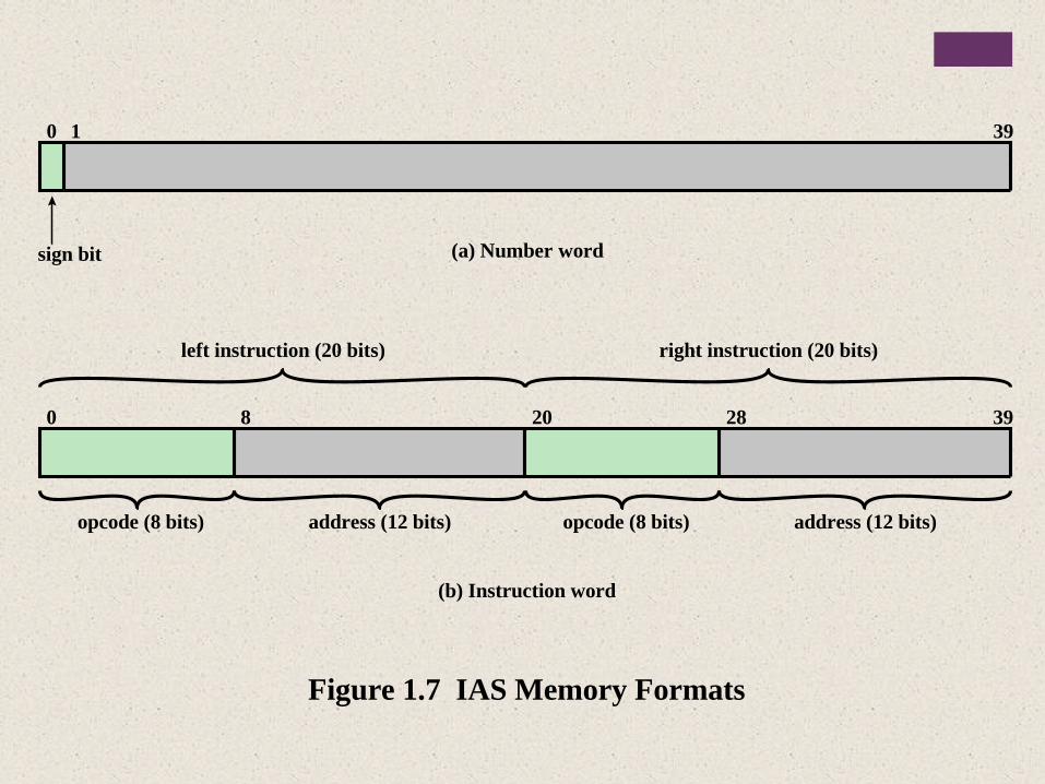
(a) Number wordsign bit
0 39
(b) Instruction word
Figure 1.7 IAS Memory Formats
opcode (8 bits) address (12 bits)
left instruction (20 bits)
0 8 20 28 39
1
right instruction (20 bits)
opcode (8 bits) address (12 bits)
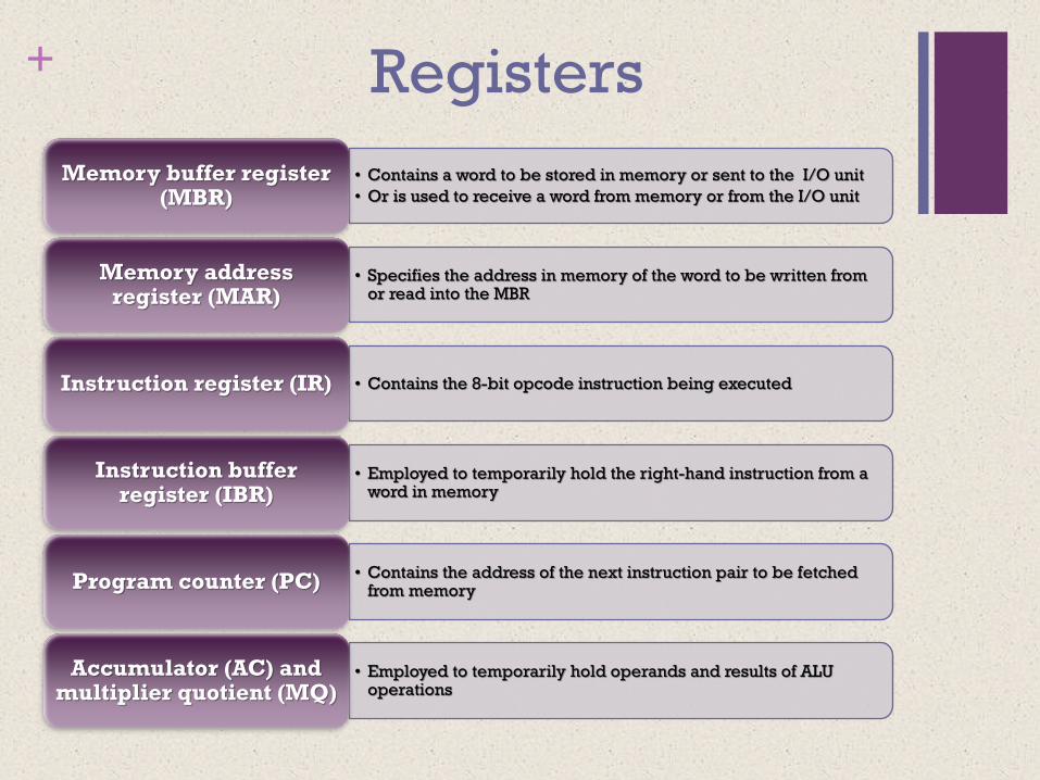
+ Registers
• Contains a word to be stored in memory or sent to the I/O unit
• Or is used to receive a word from memory or from the I/O unit
Memory buffer register (MBR)
• Specifies the address in memory of the word to be written from or read into the MBR
Memory address register (MAR)
• Contains the 8-bit opcode instruction being executedInstruction register (IR)
• Employed to temporarily hold the right-hand instruction from a word in memory
Instruction buffer register (IBR)
• Contains the address of the next instruction pair to be fetched from memoryProgram counter (PC)
• Employed to temporarily hold operands and results of ALU operations
Accumulator (AC) and multiplier quotient (MQ)

Instruction Type Opcode Symbolic
Representation Description
Data transfer
00001010 LOAD MQ Transfer contents of register MQ to the accumulator AC
00001001 LOAD MQ,M(X) Transfer contents of memory location X to
MQ
00100001 STOR M(X) Transfer contents of accumulator to memory
location X
00000001 LOAD M(X) Transfer M(X) to the accumulator
00000010 LOAD –M(X) Transfer –M(X) to the accumulator
00000011 LOAD |M(X)| Transfer absolute value of M(X) to the
accumulator
00000100 LOAD –|M(X)| Transfer –|M(X)| to the accumulator
Unconditional
branch
00001101 JUMP M(X,0:19) Take next instruction from left half of M(X)
00001110 JUMP M(X,20:39) Take next instruction from right half of M(X)
Conditional branch
00001111 JUMP+ M(X,0:19) If number in the accumulator is nonnegative,
take next instruction from left half of M(X)
00
0
1
00
0
0
JUMP
+
M(X
,20:39)
If number in the accumulator is nonnegative,
take next instruction from
right half of M(X)
Arithmetic
00000101 ADD M(X) Add M(X) to AC; put the result in AC
00000111 ADD |M(X)| Add |M(X)| to AC; put the result in AC
00000110 SUB M(X) Subtract M(X) from AC; put the result in AC
00001000 SUB |M(X)| Subtract |M(X)| from AC; put the remainder
in AC
00001011 MUL M(X) Multiply M(X) by MQ; put most significant bits of result in AC, put least significant bits
in MQ
00001100 DIV M(X) Divide AC by M(X); put the quotient in MQ and the remainder in AC
00010100 LSH Multiply accumulator by 2; i.e., shift left one
bit position
00010101 RSH Divide accumulator by 2; i.e., shift right one
position
Address modify
00010010 STOR M(X,8:19) Replace left address field at M(X) by 12 rightmost bits of AC
00010011 STOR M(X,28:39) Replace right address field at M(X) by 12
rightmost bits of AC
The IAS
Instruction Set

+History of Computers
Smaller
Cheaper
Dissipates less heat than a vacuum tube
Is a solid state device made from silicon
Was invented at Bell Labs in 1947
It was not until the late 1950’s that fully transistorized
computers were commercially available
Second Generation: Transistors
© 2016 Pearson Education, Inc., Hoboken, NJ. All rights reserved.

+Second Generation Computers
Introduced:
More complex arithmetic and logic units and
control units
The use of high-level programming languages
Provision of system software which provided the
ability to:
Load programs
Move data to peripherals
Libraries perform common computations

Third Generation: Integrated Circuits
History of Computers
1958 – the invention of the integrated circuit
Discrete component
Single, self-contained transistor
Manufactured separately, packaged in their own containers, and
soldered or wired together onto masonite-like circuit boards
Manufacturing process was expensive and cumbersome
The two most important members of the third generation
were the IBM System/360 and the DEC PDP-8
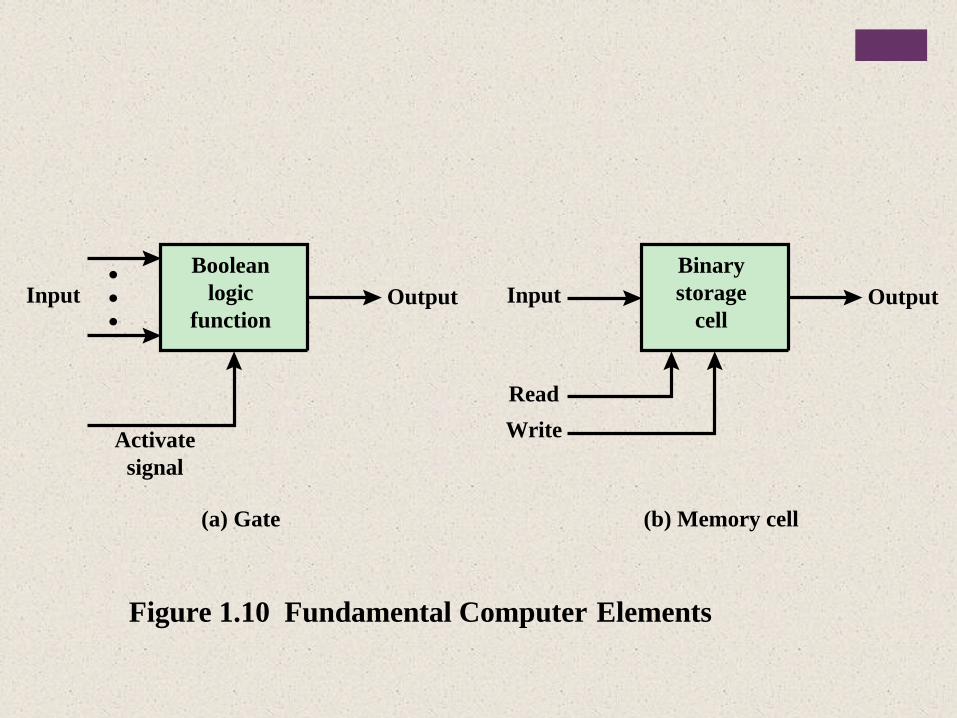
Boolean
logic
functionInput
Activate
signal
(a) Gate
Figure 1.10 Fundamental Computer Elements
Output
Binary
storage
cellInput
Read
Write
(b) Memory cell
Output

+Integrated
Circuits
A computer consists of gates,
memory cells, and
interconnections among these
elements
The gates and memory cells
are constructed of simple
digital electronic components
Data storage – provided by memory cells
Data processing – provided by gates
Data movement – the paths among components are used to move data from memory to memory and from memory through gates to memory
Control – the paths among components can carry control signals
Exploits the fact that such components as transistors, resistors, and conductors can be fabricated from a semiconductor such as silicon
Many transistors can be produced at the same time on a single wafer of silicon
Transistors can be connected with a processor metallization to form circuits

Wafer
Chip
Gate
Figure 1.11 Relationship Among Wafer, Chip, and Gate
Packaged
chip

Moore’s Law
1965; Gordon Moore – co-founder of Intel
Observed number of transistors that could be put on a single chip was doubling every year
The pace slowed to a doubling every 18
months in the 1970’s but has sustained
that rate ever since
Consequences of Moore’s law:
The cost of computer logic
and memory circuitry has
fallen at a dramatic rate
The electrical path length is
shortened, increasing operating
speed
Computer becomes smaller
and is more convenient to
use in a variety of environments
Reduction in power and
cooling requirements
Fewer interchip
connections

+ Family Characteristics
Similar or identical
instruction set
Similar or identical operating
system
Increasing speed
Increasing number of I/O
ports
Increasing memory size
Increasing cost

+
Later
Generations
LSILarge
Scale
Integration
VLSIVery Large
Scale
Integration
ULSIUltra Large
Scale
Integration
Semiconductor Memory
Microprocessors

Semiconductor Memory
Since 1970 semiconductor memory has been through 13 generations
Each generation has provided four times the storage density of the previous generation, accompanied by declining cost per bit and declining access time
In 1974 the price per bit of semiconductor memory dropped below the price per bit of core memory
There has been a continuing and rapid decline in memory cost accompanied by a corresponding
increase in physical memory density
Developments in memory and processor technologies changed the nature of computers in
less than a decade
In 1970 Fairchild produced the first relatively capacious semiconductor memory
Chip was about the size of a single core
Could hold 256 bits of memory
Non-destructive Much faster than core

+Microprocessors
The density of elements on processor chips continued to rise
More and more elements were placed on each chip so that fewer and fewer chips were needed to construct a single computer processor
1971 Intel developed 4004
First chip to contain all of the components of a CPU on a single chip
Birth of microprocessor
1972 Intel developed 8008
First 8-bit microprocessor
1974 Intel developed 8080
First general purpose microprocessor
Faster, has a richer instruction set, has a large addressing capability

Evolution of Intel Microprocessors
(a) 1970s Processors
4004 8008 8080 8086 8088
Introduced 1971 1972 1974 1978 1979
Clock speeds 108 kHz 108 kHz 2 MHz 5 MHz, 8 MHz, 10
MHz 5 MHz, 8 MHz
Bus width 4 bits 8 bits 8 bits 16 bits 8 bits
Number of
transistors 2,300 3,500 6,000 29,000 29,000
Feature size (µm)
10 8 6 3 6
Addressable
memory 640 Bytes 16 KB 64 KB 1 MB 1 MB

Evolution of Intel Microprocessors
(b) 1980s Processors
80286 386TM DX 386TM SX 486TM DX
CPU
Introduced 1982 1985 1988 1989
Clock speeds 6 MHz - 12.5
MHz 16 MHz - 33
MHz 16 MHz - 33
MHz 25 MHz - 50
MHz
Bus width 16 bits 32 bits 16 bits 32 bits
Number of transistors
134,000 275,000 275,000 1.2 million
Feature size (µm) 1.5 1 1 0.8 - 1
Addressable
memory 16 MB 4 GB 16 MB 4 GB
Virtual
memory 1 GB 64 TB 64 TB 64 TB
Cache — — — 8 kB

Evolution of Intel Microprocessors
(c) 1990s Processors
486TM SX Pentium Pentium Pro Pentium I I Introduced 1991 1993 1995 1997
Clock speeds 16 MHz - 33
MHz
60 MHz - 166
MHz,
150 MHz - 200
MHz
200 MHz - 300
MHz
Bus width 32 bits 32 bits 64 bits 64 bits
Number of
transistors 1.185 million 3.1 million 5.5 million 7.5 million
Feature size (µm) 1 0.8 0.6 0.35
Addressable
memory 4 GB 4 GB 64 GB 64 GB
Virtual memory 64 TB 64 TB 64 TB 64 TB
Cache 8 kB 8 kB 512 kB L1 and 1
MB L2 512 kB L2

Evolution of Intel Microprocessors
(d) Recent Processors
Pentium I I I Pentium 4 Core 2 Duo Core i7 EE
4960X Introduced 1999 2000 2006 2013
Clock speeds 450 - 660 MHz 1.3 - 1.8 GHz 1.06 - 1.2 GHz 4 GHz
Bus
wid
th
64 bits 64 bits 64 bits 64 bits
Number of
transistors 9.5 million 42 million 167 million 1.86 billion
Feature size (nm) 250 180 65 22
Addressable memory
64 GB 64 GB 64 GB 64 GB
Virtual memory 64 TB 64 TB 64 TB 64 TB
Cache 512 kB L2 256 kB L2 2 MB L2 1.5 MB L2/15
MB L3
Number of cores 1 1 2 6

+The Evolution of the Intel x86
Architecture
Two processor families are the Intel x86 and the ARM
architectures
Current x86 offerings represent the results of decades of
design effort on complex instruction set computers (CISCs)
An alternative approach to processor design is the reduced
instruction set computer (RISC)
ARM architecture is used in a wide variety of embedded
systems and is one of the most powerful and best-designed
RISC-based systems on the market

Highlights of the Evolution of the
Intel Product Line:
8080
• World’s first general-purpose microprocessor
• 8-bit machine, 8-bit data path to memory
• Was used in the first personal computer (Altair)
8086
• A more powerful 16-bit machine
• Has an instruction cache, or queue, that prefetches a few instructions before they are executed
• The first appearance of the x86 architecture
• The 8088 was a variant of this processor and used in IBM’s first personal computer (securing the success of Intel
80286
• Extension of the 8086 enabling addressing a 16-MB memory instead of just 1MB
80386
• Intel’s first 32-bit machine
• First Intel processor to support multitasking
80486
• Introduced the use of much more sophisticated and powerful cache technology and sophisticated instruction pipelining
• Also offered a built-in math coprocessor

Highlights of the Evolution of the
Intel Product Line:
• Intel introduced the use of superscalar techniques, which allow multiple instructions to execute in parallel
Pentium
• Continued the move into superscalar organization with aggressive use of register renaming, branch prediction, data flow analysis, and speculative execution
Pentium Pro
• Incorporated Intel MMX technology, which is designed specifically to process video, audio, and graphics data efficiently
Pentium II
•Incorporated additional floating-point instructions
•Streaming SIMD Extensions (SSE)
Pentium III
• Includes additional floating-point and other enhancements for multimedia
Pentium 4
• First Intel x86 micro-core
Core
• Extends the Core architecture to 64 bits
• Core 2 Quad provides four cores on a single chip
• More recent Core offerings have up to 10 cores per chip
• An important addition to the architecture was the Advanced Vector Extensions instruction set
Core 2

+Embedded Systems
The use of electronics and software within a product
Billions of computer systems are produced each year that are embedded within larger devices
Today many devices that use electric power have an embedded computing system
Often embedded systems are tightly coupled to their environment
This can give rise to real-time constraints imposed by the need to interact with the environment
Constraints such as required speeds of motion, required precision of measurement, and required time durations, dictate the timing of software operations
If multiple activities must be managed simultaneously this imposes more complex real-time constraints

Memory
Custom
logic
Human
interface
Diagnostic
port
Processor
D/A
Conversion
Actuators/
indicators
A/D
conversion
Sensors
Figure 1.14 Possible Organization of an Embedded System

+The Internet of Things (IoT)
Term that refers to the expanding interconnection of smart devices, ranging from appliances to tiny sensors
Is primarily driven by deeply embedded devices
Generations of deployment culminating in the IoT:
Information technology (IT)
PCs, servers, routers, firewalls, and so on, bought as IT devices by enterprise IT people and primarily using wired connectivity
Operational technology (OT)
Machines/appliances with embedded IT built by non-IT companies, such as medical machinery, SCADA, process control, and kiosks, bought as appliances by enterprise OT people and primarily using wired connectivity
Personal technology
Smartphones, tablets, and eBook readers bought as IT devices by consumers exclusively using wireless connectivity and often multiple forms of wireless connectivity
Sensor/actuator technology
Single-purpose devices bought by consumers, IT, and OT people exclusively using wireless connectivity, generally of a single form, as part of larger systems
It is the fourth generation that is usually thought of as the IoT and it is marked by the use of billions of embedded devices
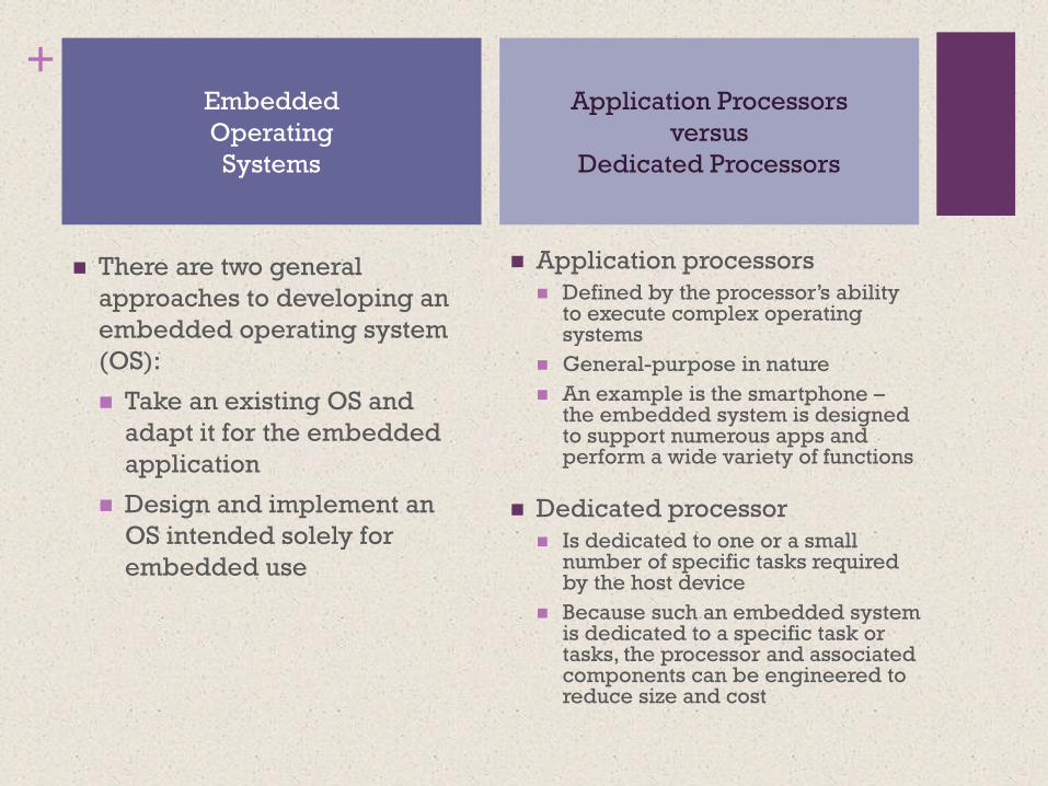
+
There are two general
approaches to developing an
embedded operating system
(OS):
Take an existing OS and
adapt it for the embedded
application
Design and implement an
OS intended solely for
embedded use
Application processors
Defined by the processor’s ability to execute complex operating systems
General-purpose in nature
An example is the smartphone –the embedded system is designed to support numerous apps and perform a wide variety of functions
Dedicated processor
Is dedicated to one or a small number of specific tasks required by the host device
Because such an embedded system is dedicated to a specific task or tasks, the processor and associated components can be engineered to reduce size and cost
Embedded
Operating
Systems
Application Processors
versus
Dedicated Processors

Figure 1.15 Typical Microcontroller Chip Elements
A/D
converter
Analog data
acquisition
Temporary
data
Processor
System
bus
RAM
D/A
converterROM
Serial I/O
portsEEPROM
Parallel I/O
portsTIMER
Program
and data
Permanent
data
Timing
functions
Analog data
transmission
Send/receive
data
Peripheral
interfaces

+Deeply Embedded Systems
Subset of embedded systems
Has a processor whose behavior is difficult to observe both by the programmer and the user
Uses a microcontroller rather than a microprocessor
Is not programmable once the program logic for the device has been burned into ROM
Has no interaction with a user
Dedicated, single-purpose devices that detect something in the environment, perform a basic level of processing, and then do something with the results
Often have wireless capability and appear in networked configurations, such as networks of sensors deployed over a large area
Typically have extreme resource constraints in terms of memory, processor size, time, and power consumption

ARM
Refers to a processor architecture that has evolved from RISC design principles and is used in embedded systems
Family of RISC-based microprocessors and microcontrollers designed by ARM Holdings, Cambridge, England
Chips are high-speed processors that are known for their small die size and low power requirements
Probably the most widely used embedded processor architecture and indeed the most widely used processor
architecture of any kind in the world
Acorn RISC Machine/Advanced RISC Machine
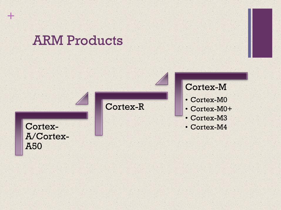
+
ARM Products
Cortex-A/Cortex-A50
Cortex-R
Cortex-M
• Cortex-M0
• Cortex-M0+
• Cortex-M3
• Cortex-M4

Figure 1.16 Typical Microcontroller Chip Based on Cortex-M3
Cortex-M3 Core
Microcontroller Chip
Cortex-M3
Processor
NVICinterface
ETMinterface
Hardwaredivider
32-bitmultiplier
32-bit ALU
Controllogic
Thumbdecode
Instructioninterface
Datainterface
ICodeinterface
Debug logic
ARMcore
DAP
NVIC ETM
Memoryprotection unit
Bus matrix
SRAM &peripheral I/F
Security Analog Interfaces Timers &Triggers Parallel I/O Ports Serial Interfaces
Peripheral bus
Core and memoryClock managementEnergy management
Cortex-M3 processor
Memoryprotec-
tion unit
Flashmemory64 kB
Voltageregula-
tor
Power-on reset
Brown-out de-tector
Voltagecompar-
ator
High fre-
quency RC
oscillator
Low fre-
quency RC
oscillator
High freq
crystal
oscillator
Low freq
crystal
oscillator
SRAMmemory64 kB
Debuginter-face
DMAcontrol-
ler
Pulsecounter
Watch-dog tmr
Lowenergy
Realtime ctr
Periphbus int
Timer/counter
Generalpurpose
I/O
ExternalInter-rupts
UART
USART
Low-energyUART
USBPin
reset
32-bit bus
A/Dcon-
verter
Hard-wareAES
D/Acon-
verter

+Cloud Computing
NIST defines cloud computing as:
“A model for enabling ubiquitous, convenient, on-demand network access to a shared pool of configurable computing resources that can be rapidly provisioned and released with minimal management effort or service provider interaction.”
You get economies of scale, professional network management, and professional security management
The individual or company only needs to pay for the storage capacity and services they need
Cloud provider takes care of security

Cloud Networking
Refers to the networks and network management functionality that must be in place to enable cloud computing
One example is the provisioning of high-performance and/or high-reliability networking between the provider and subscriber
The collection of network capabilities required to access a cloud, including making use of specialized services over the Internet, linking enterprise data center to a cloud, and using firewalls and other network security devices at critical points to enforce access security policies
Cloud Storage
Subset of cloud computing
Consists of database storage and database applications hosted remotely on cloud servers
Enables small businesses and individual users to take advantage of data storage that scales with their needs and to take advantage of a variety of database applications without having to buy, maintain, and manage the storage assets