ADuC7128/ADuC7129 Precision Analog Microcontroller ARM7TDMI MCU … · Precision Analog...
92
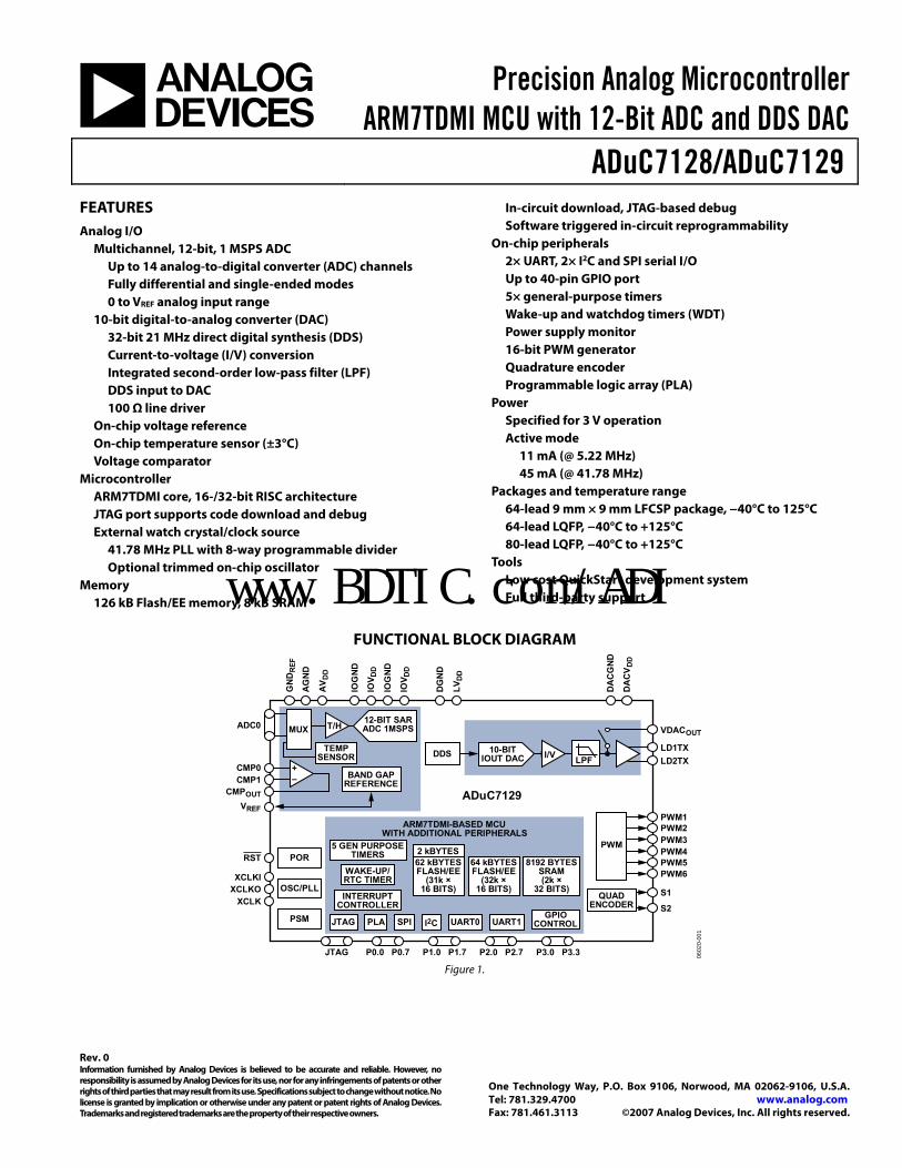
Precision Analog Microcontroller ARM7TDMI MCU with 12-Bit ADC and DDS DAC ADuC7128/ADuC7129 Rev. 0 Information furnished by Analog Devices is believed to be accurate and reliable. However, no responsibility is assumed by Analog Devices for its use, nor for any infringements of patents or other rights of third parties that may result from its use. Specifications subject to change without notice. No license is granted by implication or otherwise under any patent or patent rights of Analog Devices. Trademarks and registered trademarks are the property of their respective owners. One Technology Way, P.O. Box 9106, Norwood, MA 02062-9106, U.S.A. Tel: 781.329.4700 www.analog.com Fax: 781.461.3113 ©2007 Analog Devices, Inc. All rights reserved. FEATURES Analog I/O Multichannel, 12-bit, 1 MSPS ADC Up to 14 analog-to-digital converter (ADC) channels Fully differential and single-ended modes 0 to VREF analog input range 10-bit digital-to-analog converter (DAC) 32-bit 21 MHz direct digital synthesis (DDS) Current-to-voltage (I/V) conversion Integrated second-order low-pass filter (LPF) DDS input to DAC 100 Ω line driver On-chip voltage reference On-chip temperature sensor (±3°C) Voltage comparator Microcontroller ARM7TDMI core, 16-/32-bit RISC architecture JTAG port supports code download and debug External watch crystal/clock source 41.78 MHz PLL with 8-way programmable divider Optional trimmed on-chip oscillator Memory 126 kB Flash/EE memory, 8 kB SRAM In-circuit download, JTAG-based debug Software triggered in-circuit reprogrammability On-chip peripherals 2× UART, 2× I 2 C and SPI serial I/O Up to 40-pin GPIO port 5× general-purpose timers Wake-up and watchdog timers (WDT) Power supply monitor 16-bit PWM generator Quadrature encoder Programmable logic array (PLA) Power Specified for 3 V operation Active mode 11 mA (@ 5.22 MHz) 45 mA (@ 41.78 MHz) Packages and temperature range 64-lead 9 mm × 9 mm LFCSP package, −40°C to 125°C 64-lead LQFP, −40°C to +125°C 80-lead LQFP, −40°C to +125°C Tools Low cost QuickStart development system Full third-party support FUNCTIONAL BLOCK DIAGRAM XCLKI XCLKO RST XCLK I/V LD1TX LD2TX VDAC OUT ADuC7129 V REF ADC0 CMP OUT CMP0 CMP1 PWM4 PWM3 PWM2 PWM1 S1 S2 PWM6 PWM5 DDS LPF 12-BIT SAR ADC 1MSPS BAND GAP REFERENCE + – TEMP SENSOR MUX ARM7TDMI-BASED MCU WITH ADDITIONAL PERIPHERALS OSC/PLL POR PSM JTAG P0.0 P0.7 P1.0 P1.7 P2.0 P2.7 P3.0 P3.3 5 GEN PURPOSE TIMERS WAKE-UP/ RTC TIMER INTERRUPT CONTROLLER JTAG PLA SPI I 2 C UART0 UART1 GPIO CONTROL 8192 BYTES SRAM (2k × 32 BITS) 64 kBYTES FLASH/EE (32k × 16 BITS) 2 kBYTES GND REF AGND AV DD IOGND IOV DD IOGND IOV DD DGND LV DD DACGND DACV DD PWM QUAD ENCODER 62 kBYTES FLASH/EE (31k × 16 BITS) I/V T/H 10-BIT IOUT DAC 06020-001 Figure 1. www.BDTIC.com/ADI
Transcript of ADuC7128/ADuC7129 Precision Analog Microcontroller ARM7TDMI MCU … · Precision Analog...
Precision Analog MicrocontrollerARM7TDMI MCU with 12-Bit ADC and DDS DAC
ADuC7128/ADuC7129
Rev. 0 Information furnished by Analog Devices is believed to be accurate and reliable. However, no responsibility is assumed by Analog Devices for its use, nor for any infringements of patents or other rights of third parties that may result from its use. Specifications subject to change without notice. No license is granted by implication or otherwise under any patent or patent rights of Analog Devices. Trademarks and registered trademarks are the property of their respective owners.
One Technology Way, P.O. Box 9106, Norwood, MA 02062-9106, U.S.A.Tel: 781.329.4700 www.analog.com Fax: 781.461.3113 ©2007 Analog Devices, Inc. All rights reserved.
FEATURES Analog I/O
Multichannel, 12-bit, 1 MSPS ADC Up to 14 analog-to-digital converter (ADC) channels Fully differential and single-ended modes 0 to VREF analog input range
10-bit digital-to-analog converter (DAC) 32-bit 21 MHz direct digital synthesis (DDS) Current-to-voltage (I/V) conversion Integrated second-order low-pass filter (LPF) DDS input to DAC 100 Ω line driver
On-chip voltage reference On-chip temperature sensor (±3°C) Voltage comparator
Microcontroller ARM7TDMI core, 16-/32-bit RISC architecture JTAG port supports code download and debug External watch crystal/clock source
41.78 MHz PLL with 8-way programmable divider Optional trimmed on-chip oscillator
Memory 126 kB Flash/EE memory, 8 kB SRAM
In-circuit download, JTAG-based debug Software triggered in-circuit reprogrammability
On-chip peripherals 2× UART, 2× I2C and SPI serial I/O Up to 40-pin GPIO port 5× general-purpose timers Wake-up and watchdog timers (WDT) Power supply monitor 16-bit PWM generator Quadrature encoder Programmable logic array (PLA)
Power Specified for 3 V operation Active mode
11 mA (@ 5.22 MHz) 45 mA (@ 41.78 MHz)
Packages and temperature range 64-lead 9 mm × 9 mm LFCSP package, −40°C to 125°C 64-lead LQFP, −40°C to +125°C 80-lead LQFP, −40°C to +125°C
Tools Low cost QuickStart development system Full third-party support
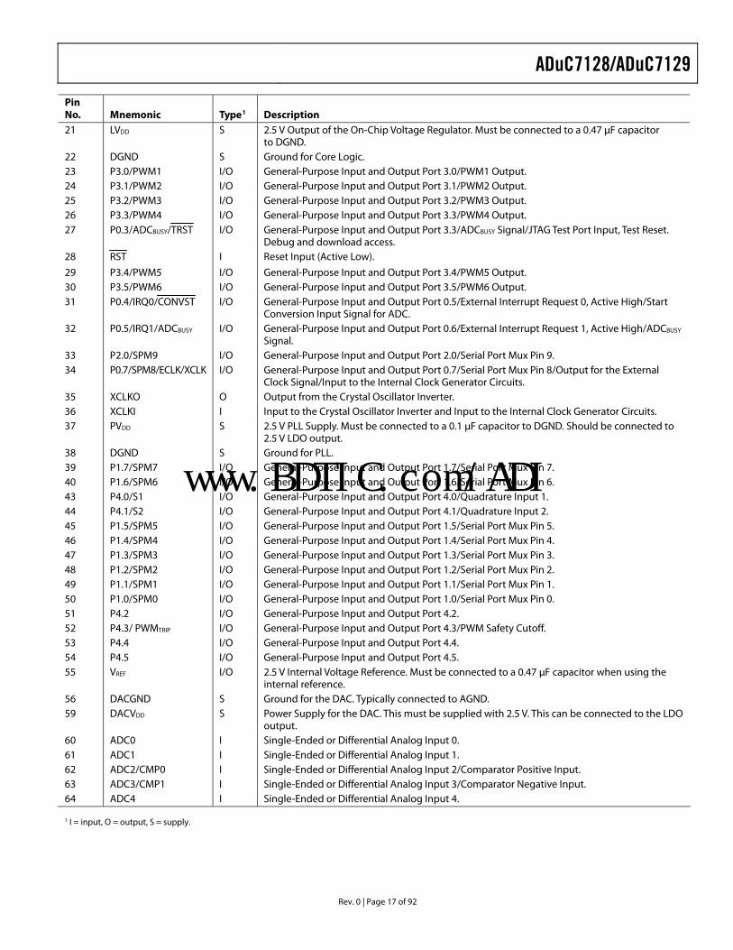
FUNCTIONAL BLOCK DIAGRAM
XCLKIXCLKO
RST
XCLK
I/VLD1TXLD2TX
VDACOUT
ADuC7129VREF
ADC0
CMPOUT
CMP0CMP1
PWM4PWM3PWM2PWM1
S1
S2
PWM6PWM5
DDSLPF
12-BIT SARADC 1MSPS
BAND GAPREFERENCE
+–
TEMPSENSOR
MUX
ARM7TDMI-BASED MCUWITH ADDITIONAL PERIPHERALS
OSC/PLL
POR
PSM
JTAG P0.0 P0.7 P1.0 P1.7 P2.0 P2.7 P3.0 P3.3
5 GEN PURPOSETIMERS
WAKE-UP/RTC TIMER
INTERRUPTCONTROLLER
JTAG PLA SPI I2C UART0 UART1GPIO
CONTROL
8192 BYTESSRAM(2k ×
32 BITS)
64 kBYTESFLASH/EE
(32k ×16 BITS)
2 kBYTES
GN
DR
EF
AG
ND
AV D
D
IOG
ND
IOV D
D
IOG
ND
IOV D
D
DG
ND
LVD
D
DA
CG
ND
DA
CV
DD
PWM
QUADENCODER
62 kBYTESFLASH/EE
(31k ×16 BITS)
I/V
T/H
10-BITIOUT DAC
0602
0-00
1
Figure 1.
www.BDTIC.com/ADI
ADuC7128/ADuC7129
Rev. 0 | Page 2 of 92
TABLE OF CONTENTS Features .............................................................................................. 1 Functional Block Diagram .............................................................. 1 Revision History ............................................................................... 2 General Description ......................................................................... 3 Specifications..................................................................................... 4
Timing Specifications .................................................................. 8 Absolute Maximum Ratings.......................................................... 15
ESD Caution................................................................................ 15 Pin Configuration and Function Descriptions........................... 16 Typical Performance Characteristics ........................................... 21 Terminology .................................................................................... 24
ADC Specifications .................................................................... 24 DAC Specifications..................................................................... 24
Overview of the ARM7TDMI Core............................................. 25 Thumb Mode (T)........................................................................ 25 Long Multiply (M)...................................................................... 25 EmbeddedICE (I) ....................................................................... 25 Exceptions ................................................................................... 25 ARM Registers ............................................................................ 25 Interrupt Latency........................................................................ 26
Memory Organization ................................................................... 27 Flash/EE Memory....................................................................... 27 SRAM........................................................................................... 27 Memory Mapped Registers ....................................................... 27 Complete MMR Listing............................................................. 28
ADC Circuit Overview .................................................................. 32 ADC Transfer Function............................................................. 32 Typical Operation....................................................................... 33 Converter Operation.................................................................. 36 Driving the Analog Inputs ........................................................ 37 Temperature Sensor ................................................................... 37 Band Gap Reference................................................................... 38
Nonvolatile Flash/EE Memory ..................................................... 39 Flash/EE Memory Overview..................................................... 39 Flash/EE Memory....................................................................... 39 Flash/EE Memory Security ....................................................... 40 Flash/EE Control Interface........................................................ 40
Execution Time from SRAM and FLASH/EE........................ 43 Reset and Remap ........................................................................ 44
Other Analog Peripherals.............................................................. 45 DAC.............................................................................................. 45 DDS .............................................................................................. 46 Power Supply Monitor ............................................................... 47 Comparator ................................................................................. 47 Oscillator and PLL—Power Control........................................ 49
Digital Peripherals.......................................................................... 51 PWM General Overview........................................................... 51 PWM Convert Start Control .................................................... 52 General-Purpose I/O ................................................................. 55 Serial Port Mux........................................................................... 57 UART Serial Interface................................................................ 57 Serial Peripheral Interface......................................................... 63 I2C-Compatible Interfaces......................................................... 65 I2C Registers ................................................................................ 65 Programmable Logic Array (PLA)........................................... 69
Processor Reference Peripherals................................................... 72 Interrupt System......................................................................... 72 Timers .......................................................................................... 73 Timer0—Lifetime Timer........................................................... 73 Timer1—General-Purpose Timer ........................................... 75 Timer2—Wake-Up Timer......................................................... 77 Timer3—Watchdog Timer........................................................ 79 Timer4—General-Purpose Timer ........................................... 81 External Memory Interfacing ................................................... 83 Timing Diagrams ....................................................................... 84
Hardware Design Considerations ................................................ 87 Power Supplies ............................................................................ 87 Grounding and Board Layout Recommendations................. 87 Clock Oscillator .......................................................................... 88 Power-On Reset Operation....................................................... 89
Development Tools......................................................................... 90 In-Circuit Serial Downloader................................................... 90
Outline Dimensions ....................................................................... 91 Ordering Guide .......................................................................... 92
REVISION HISTORY 4/07—Revision 0: Initial Version
www.BDTIC.com/ADI
ADuC7128/ADuC7129
Rev. 0 | Page 3 of 92
GENERAL DESCRIPTION The ADuC7128/ADuC7129 are fully integrated, 1 MSPS, 12-bit data acquisition systems incorporating a high performance, multi-channel analog-to-digital converter (ADC), DDS with line driver, 16-/32-bit MCU, and Flash/EE memory on a single chip.
The ADC consists of up to 14 single-ended inputs. The ADC can operate in single-ended or differential input modes. The ADC input voltage is 0 to VREF. Low drift band gap reference, temperature sensor, and voltage comparator complete the ADC peripheral set.
The ADuC7128/ADuC7129 integrate a differential line driver output. This line driver transmits a sine wave whose values are calculated by an on-chip DDS or a voltage output determined by the DACDAT MMR.
The devices operate from an on-chip oscillator and PLL, generating an internal high frequency clock of 41.78 MHz. This clock is routed through a programmable clock divider from which the MCU core clock operating frequency is generated.
The microcontroller core is an ARM7TDMI®, 16-/32-bit reduced instruction set computer (RISC), offering up to 41 MIPS peak performance. There are 126 kB of nonvolatile Flash/EE provided on-chip, as well as 8 kB of SRAM. The ARM7TDMI core views all memory and registers as a single linear array.
On-chip factory firmware supports in-circuit serial download via the UART serial interface port, and nonintrusive emulation is also supported via the JTAG interface. These features are incorporated into a low cost QuickStart™ development system supporting this MicroConverter® family.
The parts operate from 3.0 V to 3.6 V and are specified over an industrial temperature range of −40°C to +125°C. When operating at 41.78 MHz, the power dissipation is 135 mW. The line driver output, if enabled, consumes an additional 30 mW.
www.BDTIC.com/ADI
ADuC7128/ADuC7129
Rev. 0 | Page 4 of 92
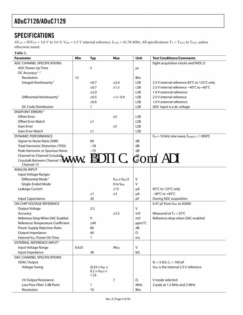
SPECIFICATIONS AVDD = IOVDD = 3.0 V to 3.6 V, VREF = 2.5 V internal reference, fCORE = 41.78 MHz. All specifications TA = TMAX to TMIN, unless otherwise noted.
Table 1. Parameter Min Typ Max Unit Test Conditions/Comments ADC CHANNEL SPECIFICATIONS Eight acquisition clocks and fADC/2
ADC Power-Up Time 5 μs DC Accuracy1, 2
Resolution 12 Bits Integral Nonlinearity3 ±0.7 ±2.0 LSB 2.5 V internal reference 85°C to 125°C only ±0.7 ±1.5 LSB 2.5 V internal reference −40°C to +85°C
±2.0 LSB 1.0 V external reference Differential Nonlinearity3 ±0.5 +1/−0.9 LSB 2.5 V internal reference ±0.6 LSB 1.0 V external reference DC Code Distribution 1 LSB ADC input is a dc voltage
ENDPOINT ERRORS4 Offset Error ±5 LSB Offset Error Match ±1 LSB Gain Error ±5 LSB Gain Error Match ±1 LSB
DYNAMIC PERFORMANCE FIN = 10 kHz sine wave, fSAMPLE = 1 MSPS Signal-to-Noise Ratio (SNR) 69 dB Total Harmonic Distortion (THD) −78 dB Peak Harmonic or Spurious Noise −75 dB Channel-to-Channel Crosstalk −80 dB Crosstalk Between Channel 12 and
Channel 13 −60 dB
ANALOG INPUT Input Voltage Ranges
Differential Mode5 VCM ± VREF/2 V Single-Ended Mode 0 to VREF V
Leakage Current ±15 μA 85°C to 125°C only ±1 ±3 μA −40°C to +85°C Input Capacitance 20 pF During ADC acquisition
ON-CHIP VOLTAGE REFERENCE 0.47 μF from VREF to AGND Output Voltage 2.5 V Accuracy ±2.5 mV Measured at TA = 25°C Reference Drop When DAC Enabled 9 mV Reference drop when DAC enabled Reference Temperature Coefficient ±40 ppm/°C Power Supply Rejection Ratio 80 dB Output Impedance 40 Ω Internal VREF Power-On Time 1 ms
EXTERNAL REFERENCE INPUT6 Input Voltage Range 0.625 AVDD V Input Impedance 38 kΩ
DAC CHANNEL SPECIFICATIONS VDAC Output RL = 5 kΩ, CL = 100 pF
Voltage Swing (0.33 × VREF ± 0.2 × VREF) × 1.33
VREF is the internal 2.5 V reference
I/V Output Resistance 7 Ω V mode selected Low-Pass Filter 3 dB Point 1 MHz 2-pole at 1.5 MHz and 2 MHz Resolution 10 Bits
www.BDTIC.com/ADI
ADuC7128/ADuC7129
Rev. 0 | Page 5 of 92
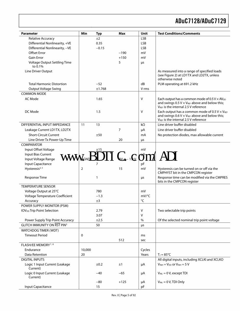
Parameter Min Typ Max Unit Test Conditions/Comments Relative Accuracy ±2 LSB Differential Nonlinearity, +VE 0.35 LSB Differential Nonlinearity, −VE −0.15 LSB Offset Error −190 mV Gain Error +150 mV Voltage Output Settling Time
to 0.1% 5 μs
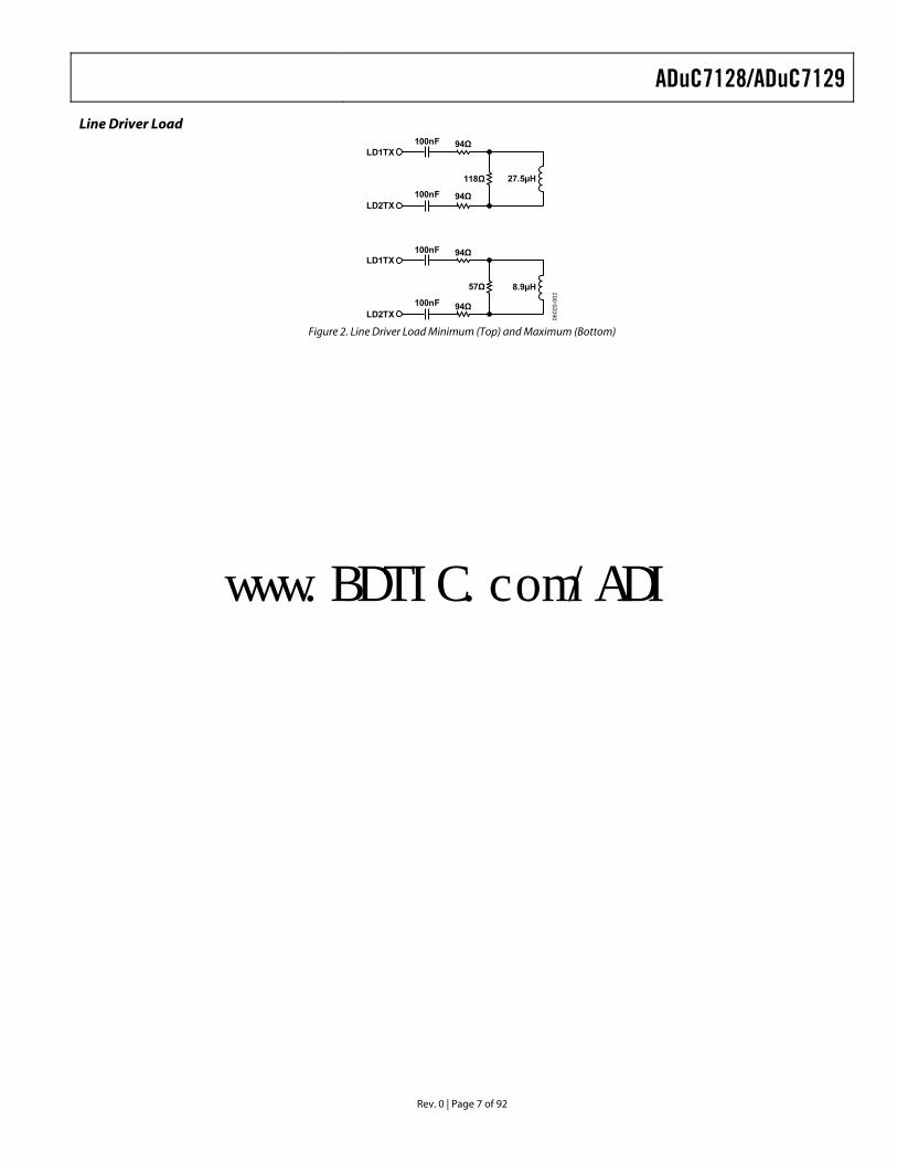
Line Driver Output As measured into a range of specified loads (see Figure 2) at LD1TX and LD2TX, unless otherwise noted
Total Harmonic Distortion −52 dB PLM operating at 691.2 kHz Output Voltage Swing ±1.768 V rms
COMMON MODE
AC Mode 1.65 V Each output has a common mode of 0.5 V × AVDD and swings 0.5 V × VREF above and below this; VREF is the internal 2.5 V reference
DC Mode 1.5 V Each output has a common mode of 0.5 V × VREF and swings 0.6 V × VREF above and below this; VREF is the internal 2.5 V reference
DIFFERENTIAL INPUT IMPEDANCE 11 13 kΩ Line driver buffer disabled
Leakage Current LD1TX, LD2TX 7 μA Line driver buffer disabled
Short-Circuit Current ±50 mA No protection diodes, max allowable current Line Driver Tx Power-Up Time 20 μs
COMPARATOR Input Offset Voltage ±15 mV Input Bias Current 1 μA Input Voltage Range AGND AVDD − 1.2 V Input Capacitance 7 pF Hysteresis3, 5 2 15 mV Hysteresis can be turned on or off via the
CMPHYST bit in the CMPCON register Response Time 1 μs Response time can be modified via the CMPRES
bits in the CMPCON register TEMPERATURE SENSOR
Voltage Output at 25°C 780 mV Voltage Temperature Coefficient −1.3 mV/°C Accuracy ±3 °C
POWER SUPPLY MONITOR (PSM) IOVDD Trip Point Selection 2.79 V Two selectable trip points
3.07 V Power Supply Trip Point Accuracy ±2.5 % Of the selected nominal trip point voltage
GLITCH IMMUNITY ON RST PIN3 50 μs
WATCHDOG TIMER (WDT) Timeout Period 0 ms 512 sec
FLASH/EE MEMORY7, 8 Endurance 10,000 Cycles Data Retention 20 Years TJ = 85°C
DIGITAL INPUTS All digital inputs, including XCLKI and XCLKO Logic 1 Input Current (Leakage
Current) ±0.2 ±1 μA VINH = VDD or VINH = 5 V
Logic 0 Input Current (Leakage Current)
−40 −65 μA VINL = 0 V, except TDI
−80 +125 μA VINL = 0 V, TDI Only Input Capacitance 15 pF
www.BDTIC.com/ADI
ADuC7128/ADuC7129
Rev. 0 | Page 6 of 92
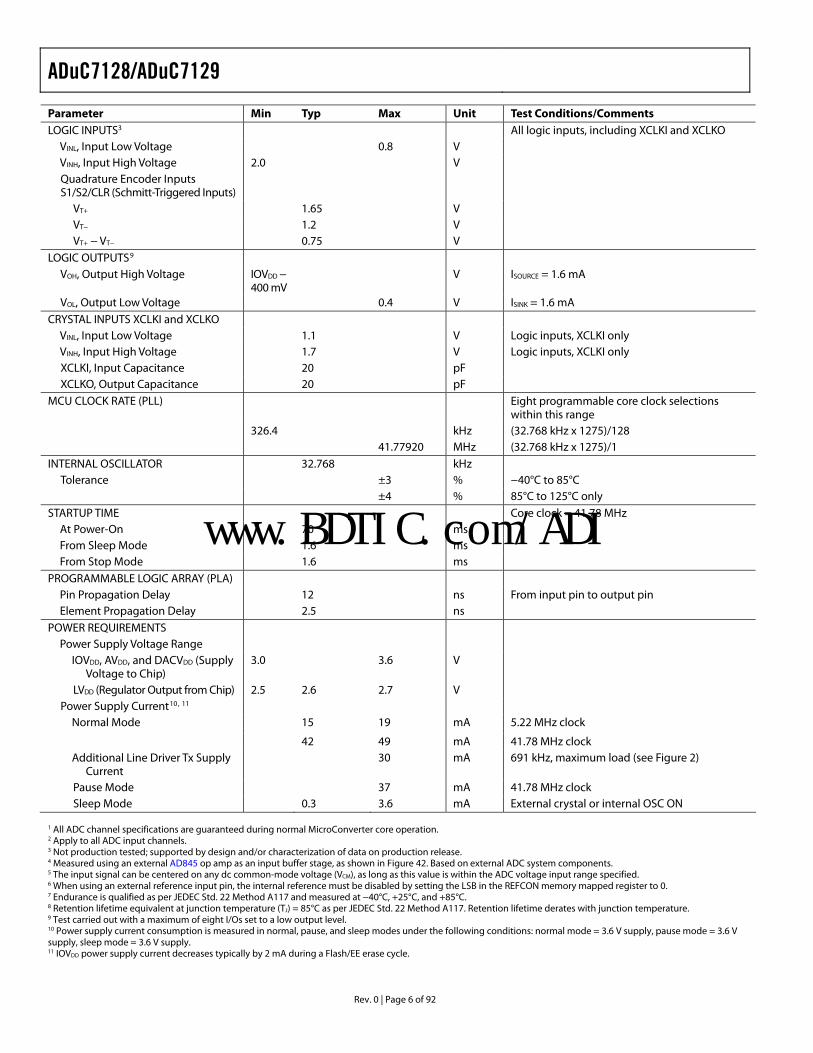
Parameter Min Typ Max Unit Test Conditions/Comments LOGIC INPUTS3 All logic inputs, including XCLKI and XCLKO
VINL, Input Low Voltage 0.8 V VINH, Input High Voltage 2.0 V Quadrature Encoder Inputs S1/S2/CLR (Schmitt-Triggered Inputs)
VT+ 1.65 V VT− 1.2 V VT+ − VT− 0.75 V
LOGIC OUTPUTS9 VOH, Output High Voltage IOVDD −
400 mV V ISOURCE = 1.6 mA
VOL, Output Low Voltage 0.4 V ISINK = 1.6 mA CRYSTAL INPUTS XCLKI and XCLKO
VINL, Input Low Voltage 1.1 V Logic inputs, XCLKI only VINH, Input High Voltage 1.7 V Logic inputs, XCLKI only XCLKI, Input Capacitance 20 pF XCLKO, Output Capacitance 20 pF
MCU CLOCK RATE (PLL) Eight programmable core clock selections within this range
326.4 kHz (32.768 kHz x 1275)/128 41.77920 MHz (32.768 kHz x 1275)/1 INTERNAL OSCILLATOR 32.768 kHz
Tolerance ±3 % −40°C to 85°C ±4 % 85°C to 125°C only
STARTUP TIME Core clock = 41.78 MHz At Power-On 70 ms From Sleep Mode 1.6 ms From Stop Mode 1.6 ms
PROGRAMMABLE LOGIC ARRAY (PLA) Pin Propagation Delay 12 ns From input pin to output pin Element Propagation Delay 2.5 ns
POWER REQUIREMENTS Power Supply Voltage Range
IOVDD, AVDD, and DACVDD (Supply Voltage to Chip)
3.0 3.6 V
LVDD (Regulator Output from Chip) 2.5 2.6 2.7 V Power Supply Current10, 11
Normal Mode 15 19 mA 5.22 MHz clock
42 49 mA 41.78 MHz clock Additional Line Driver Tx Supply
Current 30 mA 691 kHz, maximum load (see Figure 2)
Pause Mode 37 mA 41.78 MHz clock Sleep Mode 0.3 3.6 mA External crystal or internal OSC ON
1 All ADC channel specifications are guaranteed during normal MicroConverter core operation. 2 Apply to all ADC input channels. 3 Not production tested; supported by design and/or characterization of data on production release. 4 Measured using an external AD845 op amp as an input buffer stage, as shown in Figure 42. Based on external ADC system components. 5 The input signal can be centered on any dc common-mode voltage (VCM), as long as this value is within the ADC voltage input range specified. 6 When using an external reference input pin, the internal reference must be disabled by setting the LSB in the REFCON memory mapped register to 0. 7 Endurance is qualified as per JEDEC Std. 22 Method A117 and measured at −40°C, +25°C, and +85°C. 8 Retention lifetime equivalent at junction temperature (TJ) = 85°C as per JEDEC Std. 22 Method A117. Retention lifetime derates with junction temperature. 9 Test carried out with a maximum of eight I/Os set to a low output level. 10 Power supply current consumption is measured in normal, pause, and sleep modes under the following conditions: normal mode = 3.6 V supply, pause mode = 3.6 V supply, sleep mode = 3.6 V supply. 11 IOVDD power supply current decreases typically by 2 mA during a Flash/EE erase cycle.
www.BDTIC.com/ADI
ADuC7128/ADuC7129
Rev. 0 | Page 7 of 92
Line Driver Load 94Ω
27.5µH
8.9µH
LD1TX
LD2TX
100nF
100nF
100nF
100nF
LD1TX
LD2TX
94Ω
94Ω
57Ω
94Ω
118Ω
0602
0-00
2
Figure 2. Line Driver Load Minimum (Top) and Maximum (Bottom)
www.BDTIC.com/ADI
ADuC7128/ADuC7129
Rev. 0 | Page 8 of 92
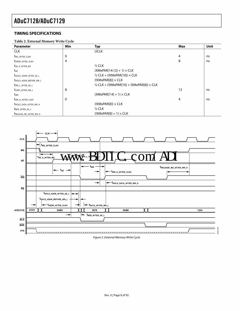
TIMING SPECIFICATIONS
Table 2. External Memory Write Cycle Parameter Min Typ Max Unit CLK UCLK tMS_AFTER_CLKH 0 4 ns tADDR_AFTER_CLKH 4 8 ns tAE_H_AFTER_MS ½ CLK tAE (XMxPAR[14:12] + 1) × CLK tHOLD_ADDR_AFTER_AE_L ½ CLK + (!XMxPAR[10]) × CLK tHOLD_ADDR_BEFORE_WR_L (!XMxPAR[8]) × CLK tWR_L_AFTER_AE_L ½ CLK + (!XMxPAR[10] + !XMxPAR[8]) × CLK tDATA_AFTER_WR_L 8 12 ns tWR (XMxPAR[7:4] + 1) × CLK tWR_H_AFTER_CLKH 0 4 ns tHOLD_DATA_AFTER_WR_H (!XMxPAR[8]) × CLK tBEN_AFTER_AE_L ½ CLK tRELEASE_MS_AFTER_WR_H (!XMxPAR[8] + 1) × CLK
0602
0-06
5
CLK
CLK
tMS_AFTER_CLKH
tAE_H_AFTER_MS
tAE
tWR_L_AFTER_AE_L
MS
AE
WS
RS
A/D[15:0] FFFF 9ABC 5678 9ABE 1234
BLE
BHE
A16
tWR
tWR_H_AFTER_CLKH
tHOLD_DATA_AFTER_WR_H
tHOLD_ADDR_AFTER_AE_L
tHOLD_ADDR_BEFORE_WR_L
tDATA_AFTER_WR_L
tBEN_AFTER_AE_L
tADDR_AFTER_CLKH
tRELEASE_MS_AFTER_WR_H
Figure 3. External Memory Write Cycle
www.BDTIC.com/ADI
ADuC7128/ADuC7129
Rev. 0 | Page 9 of 92
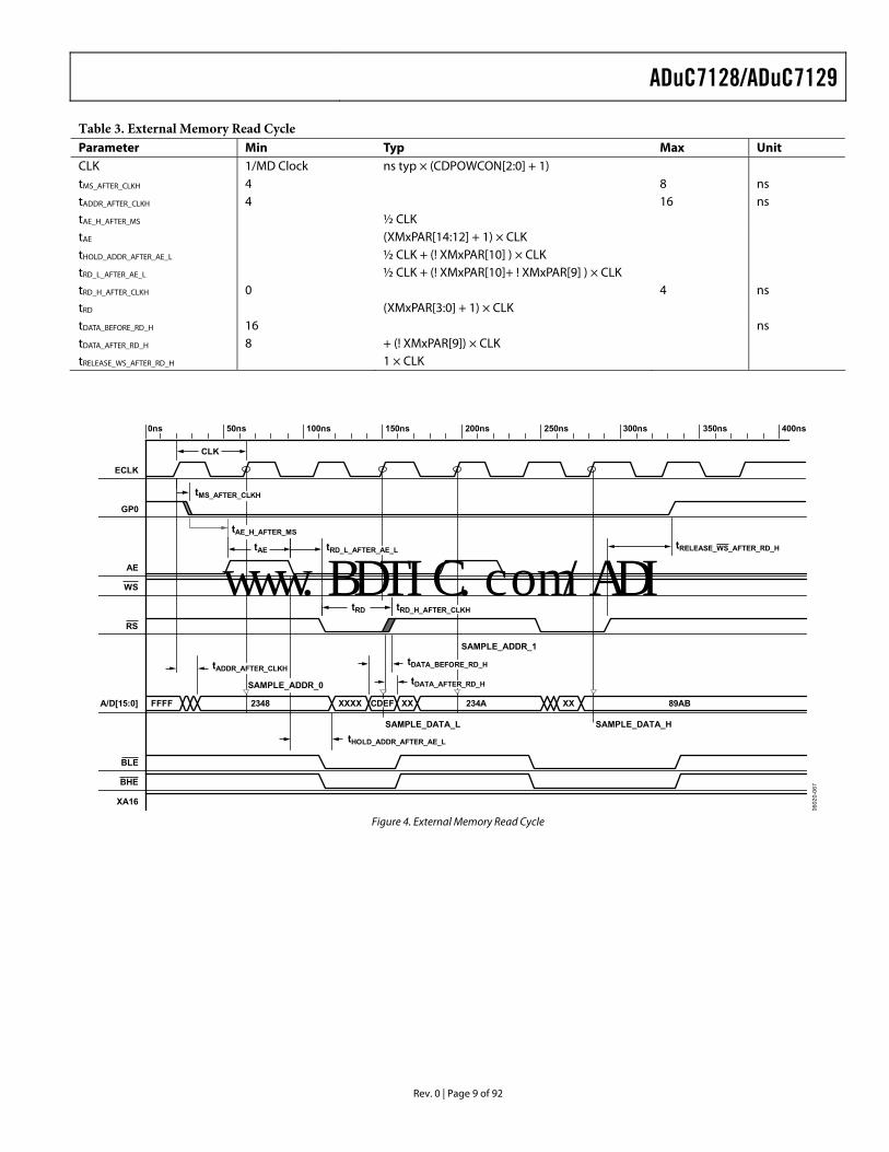
Table 3. External Memory Read Cycle Parameter Min Typ Max Unit CLK 1/MD Clock ns typ × (CDPOWCON[2:0] + 1) tMS_AFTER_CLKH 4 8 ns tADDR_AFTER_CLKH 4 16 ns tAE_H_AFTER_MS ½ CLK tAE (XMxPAR[14:12] + 1) × CLK tHOLD_ADDR_AFTER_AE_L ½ CLK + (! XMxPAR[10] ) × CLK tRD_L_AFTER_AE_L ½ CLK + (! XMxPAR[10]+ ! XMxPAR[9] ) × CLK tRD_H_AFTER_CLKH 0 4 ns tRD (XMxPAR[3:0] + 1) × CLK tDATA_BEFORE_RD_H 16 ns tDATA_AFTER_RD_H 8 + (! XMxPAR[9]) × CLK tRELEASE_WS_AFTER_RD_H 1 × CLK
0602
0-06
7
0ns 50ns 100ns 150ns 200ns 250ns 300ns 350ns 400ns
ECLK
GP0
AE
WS
RS
A/D[15:0]
BLE
BHE
XA16
FFFF 2348 XXXX CDEF XX 234A XX 89AB
CLK
tAE_H_AFTER_MS
tAE
tHOLD_ADDR_AFTER_AE_L
tRD_L_AFTER_AE_L
tRD tRD_H_AFTER_CLKH
tADDR_AFTER_CLKH
tRELEASE_WS_AFTER_RD_H
tDATA_BEFORE_RD_H
tDATA_AFTER_RD_H
SAMPLE_DATA_HSAMPLE_DATA_L
SAMPLE_ADDR_0
SAMPLE_ADDR_1
tMS_AFTER_CLKH
Figure 4. External Memory Read Cycle
www.BDTIC.com/ADI
ADuC7128/ADuC7129
Rev. 0 | Page 10 of 92
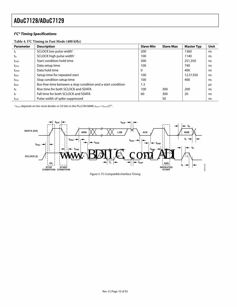
I2C® Timing Specifications
Table 4. I P
2PC Timing in Fast Mode (400 kHz)
Parameter Description Slave Min Slave Max Master Typ Unit tL SCLOCK low pulse width1 200 1360 ns tH SCLOCK high pulse width1 100 1140 ns tSHD Start condition hold time 300 251,350 ns tDSU Data setup time 100 740 ns tDHD Data hold time 0 400 ns tRSU Setup time for repeated start 100 12.51350 ns tPSU Stop condition setup time 100 400 ns tBUF Bus-free time between a stop condition and a start condition 1.3 μs tR Rise time for both SCLOCK and SDATA 100 300 200 ns tF Fall time for both SCLOCK and SDATA 60 300 20 ns tSUP Pulse width of spike suppressed 50 ns 1 tHCLK depends on the clock divider or CD bits in the PLLCON MMR, tHCLK = tUCLK/2CD.
SDATA (I/O)
tBUF
MSB LSB ACK MSB
1982–71SCLOCK (I)
PSSTOP
CONDITIONSTART
CONDITION
S(R)REPEATED
START
tSUPtR
tF
tF
tRtH
tL tSUP
tDSUtDHD
tRSU
tDHD
tDSU
tSHD
tPSU
0602
0-00
3
Figure 5. I P
2PC-Compatible Interface Timing
www.BDTIC.com/ADI
ADuC7128/ADuC7129
Rev. 0 | Page 11 of 92
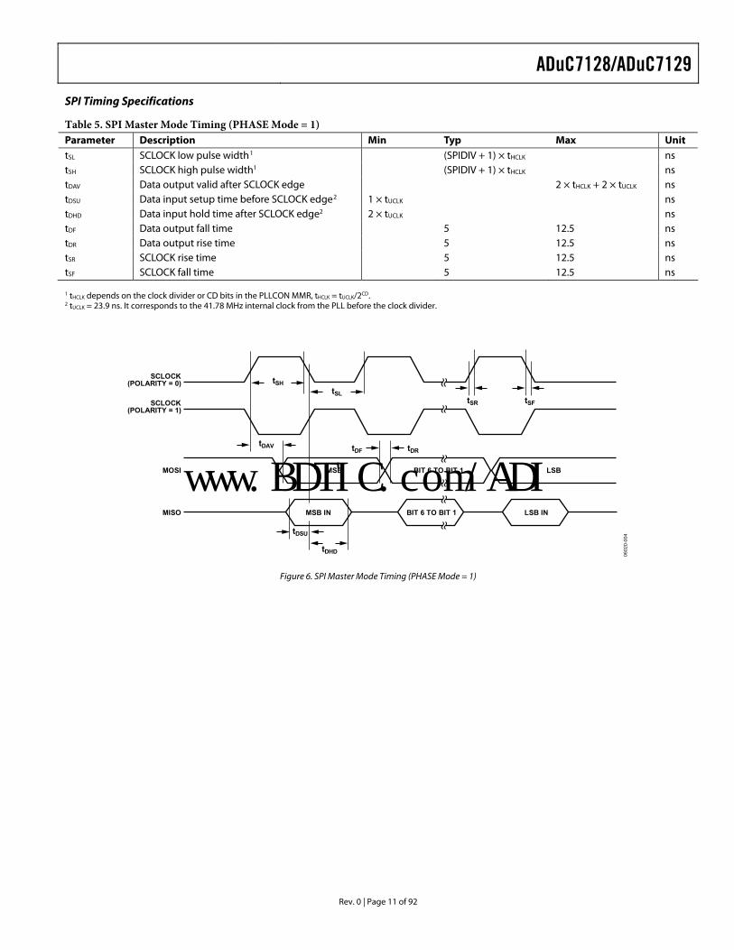
SPI Timing Specifications
Table 5. SPI Master Mode Timing (PHASE Mode = 1) Parameter Description Min Typ Max Unit tSL SCLOCK low pulse width1 (SPIDIV + 1) × tHCLK ns tSH SCLOCK high pulse width1 (SPIDIV + 1) × tHCLK ns tDAV Data output valid after SCLOCK edge 2 × tHCLK + 2 × tUCLK ns tDSU Data input setup time before SCLOCK edge2 1 × tUCLK ns tDHD Data input hold time after SCLOCK edge2 2 × tUCLK ns tDF Data output fall time 5 12.5 ns tDR Data output rise time 5 12.5 ns tSR SCLOCK rise time 5 12.5 ns tSF SCLOCK fall time 5 12.5 ns 1 tHCLK depends on the clock divider or CD bits in the PLLCON MMR, tHCLK = tUCLK/2CD. 2 tUCLK = 23.9 ns. It corresponds to the 41.78 MHz internal clock from the PLL before the clock divider.
SCLOCK(POLARITY = 0)
SCLOCK(POLARITY = 1)
MOSI MSB BIT 6 TO BIT 1 LSB
MISO MSB IN BIT 6 TO BIT 1 LSB IN
tSHtSL
tSR tSF
tDRtDFtDAV
tDSU
tDHD 0602
0-00
4
Figure 6. SPI Master Mode Timing (PHASE Mode = 1)
www.BDTIC.com/ADI
ADuC7128/ADuC7129
Rev. 0 | Page 12 of 92
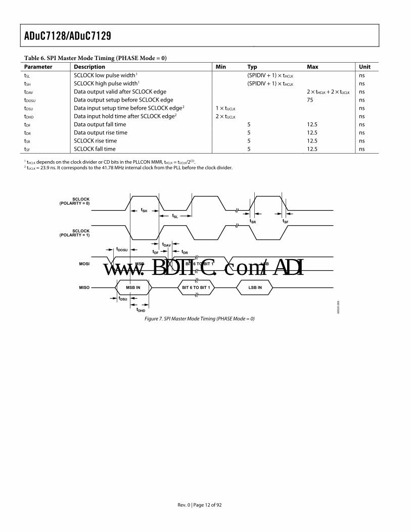
Table 6. SPI Master Mode Timing (PHASE Mode = 0) Parameter Description Min Typ Max Unit tSL SCLOCK low pulse width1 (SPIDIV + 1) × tHCLK ns tSH SCLOCK high pulse width1 (SPIDIV + 1) × tHCLK ns tDAV Data output valid after SCLOCK edge 2 × tHCLK + 2 × tUCLK ns tDOSU Data output setup before SCLOCK edge 75 ns tDSU Data input setup time before SCLOCK edge2 1 × tUCLK ns tDHD Data input hold time after SCLOCK edge2 2 × tUCLK ns tDF Data output fall time 5 12.5 ns tDR Data output rise time 5 12.5 ns tSR SCLOCK rise time 5 12.5 ns tSF SCLOCK fall time 5 12.5 ns 1 tHCLK depends on the clock divider or CD bits in the PLLCON MMR, tHCLK = tUCLK/2CD. 2 tUCLK = 23.9 ns. It corresponds to the 41.78 MHz internal clock from the PLL before the clock divider.
SCLOCK(POLARITY = 0)
SCLOCK(POLARITY = 1)
tSHtSL
tSR tSF
MOSI MSB BIT 6 TO BIT 1 LSB
MISO MSB IN BIT 6 TO BIT 1 LSB IN
tDRtDF
tDAVtDOSU
tDSU
tDHD 0602
0-00
5
Figure 7. SPI Master Mode Timing (PHASE Mode = 0)
www.BDTIC.com/ADI
ADuC7128/ADuC7129
Rev. 0 | Page 13 of 92
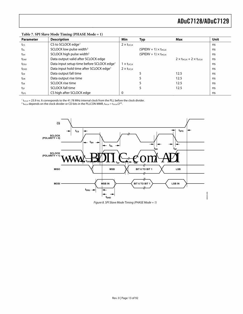
Table 7. SPI Slave Mode Timing (PHASE Mode = 1) Parameter Description Min Typ Max Unit tCS CS to SCLOCK edge1 2 × tUCLK ns tSL SCLOCK low pulse width2 (SPIDIV + 1) × tHCLK ns tSH SCLOCK high pulse width2 (SPIDIV + 1) × tHCLK ns tDAV Data output valid after SCLOCK edge 2 × tHCLK + 2 × tUCLK ns tDSU Data input setup time before SCLOCK edge1 1 × tUCLK ns tDHD Data input hold time after SCLOCK edge1 2 × tUCLK ns tDF Data output fall time 5 12.5 ns tDR Data output rise time 5 12.5 ns tSR SCLOCK rise time 5 12.5 ns tSF SCLOCK fall time 5 12.5 ns tSFS CS high after SCLOCK edge 0 ns 1 tUCLK = 23.9 ns. It corresponds to the 41.78 MHz internal clock from the PLL before the clock divider. 2 tHCLK depends on the clock divider or CD bits in the PLLCON MMR, tHCLK = tUCLK/2CD.
SCLOCK(POLARITY = 0)
CS
SCLOCK(POLARITY = 1)
tSHtSL
tSR tSF
tSFS
MISO MSB BIT 6 TO BIT 1 LSB
MOSI MSB IN BIT 6 TO BIT 1 LSB IN
tCS
tDHD
tDSU
tDAV tDRtDF
0602
0-00
6
Figure 8. SPI Slave Mode Timing (PHASE Mode = 1)
www.BDTIC.com/ADI
ADuC7128/ADuC7129
Rev. 0 | Page 14 of 92
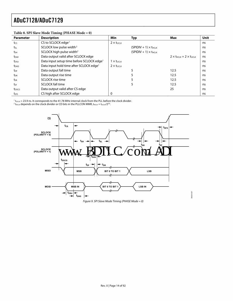
Table 8. SPI Slave Mode Timing (PHASE Mode = 0) Parameter Description Min Typ Max Unit tCS CS to SCLOCK edge1 2 × tUCLK ns tSL SCLOCK low pulse width2 (SPIDIV + 1) × tHCLK ns tSH SCLOCK high pulse width2 (SPIDIV + 1) × tHCLK ns tDAV Data output valid after SCLOCK edge 2 × tHCLK + 2 × tUCLK ns tDSU Data input setup time before SCLOCK edge1 1 × tUCLK ns tDHD Data input hold time after SCLOCK edge1 2 × tUCLK ns tDF Data output fall time 5 12.5 ns tDR Data output rise time 5 12.5 ns tSR SCLOCK rise time 5 12.5 ns tSF SCLOCK fall time 5 12.5 ns tDOCS Data output valid after CS edge 25 ns tSFS CS high after SCLOCK edge 0 ns 1 tUCLK = 23.9 ns. It corresponds to the 41.78 MHz internal clock from the PLL before the clock divider. 2 tHCLK depends on the clock divider or CD bits in the PLLCON MMR, tHCLK = tUCLK/2CD.
SCLOCK(POLARITY = 0)
CS
SCLOCK(POLARITY = 1)
tSH tSLtSR tSF
tSFS
MISO
MOSI
tCS
MSB IN BIT 6 TO BIT 1 LSB IN
tDHD
tDSU
MSB BIT 6 TO BIT 1 LSB
tDOCS
tDAV
tDRtDF
0602
0-00
7
Figure 9. SPI Slave Mode Timing (PHASE Mode = 0)
www.BDTIC.com/ADI
ADuC7128/ADuC7129
Rev. 0 | Page 15 of 92
ABSOLUTE MAXIMUM RATINGSDVDD = IOVDD, AGND = REFGND = DACGND = GNDREF. TA = 25°C, unless otherwise noted.
Table 9.
Stresses above those listed under Absolute Maximum Ratings may cause permanent damage to the device. This is a stress rating only; functional operation of the device at these or any other conditions above those indicated in the operational section of this specification is not implied. Exposure to absolute maximum rating conditions for extended periods may affect device reliability.
Only one absolute maximum rating can be applied at any one time.
ESD CAUTION
Parameter Rating AVDD to DVDD −0.3 V to +0.3 V AGND to DGND −0.3 V to +0.3 V IOVDD to IOGND, AVDD to AGND −0.3 V to +6 V Digital Input Voltage to IOGND −0.3 V to IOVDD + 0.3 V Digital Output Voltage to IOGND −0.3 V to IOVDD + 0.3 V VREF to AGND −0.3 V to AVDD + 0.3 V Analog Inputs to AGND −0.3 V to AVDD + 0.3 V Analog Output to AGND −0.3 V to AVDD + 0.3 V Operating Temperature Range
Industrial –40°C to +125°C Storage Temperature Range –65°C to +150°C Junction Temperature 150°C
θJA Thermal Impedance
64-Lead LFCSP 24°C/W 64-Lead LQFP 47°C/W 80-Lead LQFP 38°C/W
Peak Solder Reflow Temperature SnPb Assemblies (10 sec to 30 sec) 240°C RoHS Compliant Assemblies
(20 sec to 40 sec) 260°C
www.BDTIC.com/ADI
ADuC7128/ADuC7129
Rev. 0 | Page 16 of 92
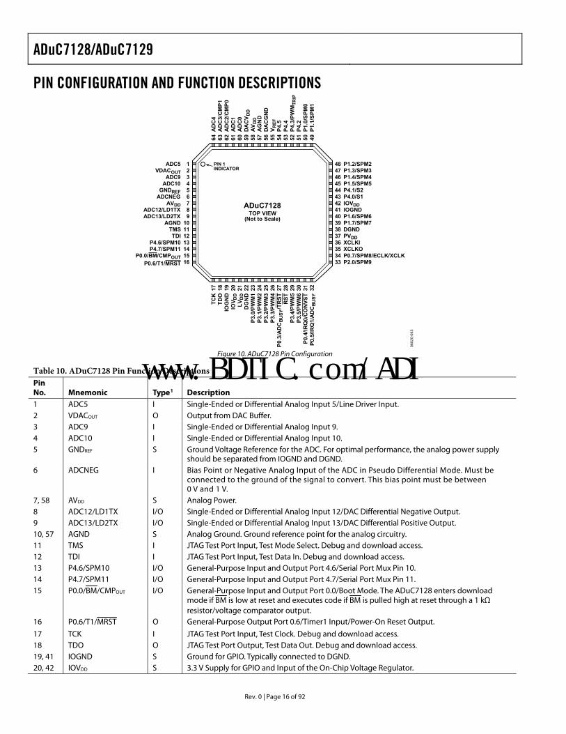
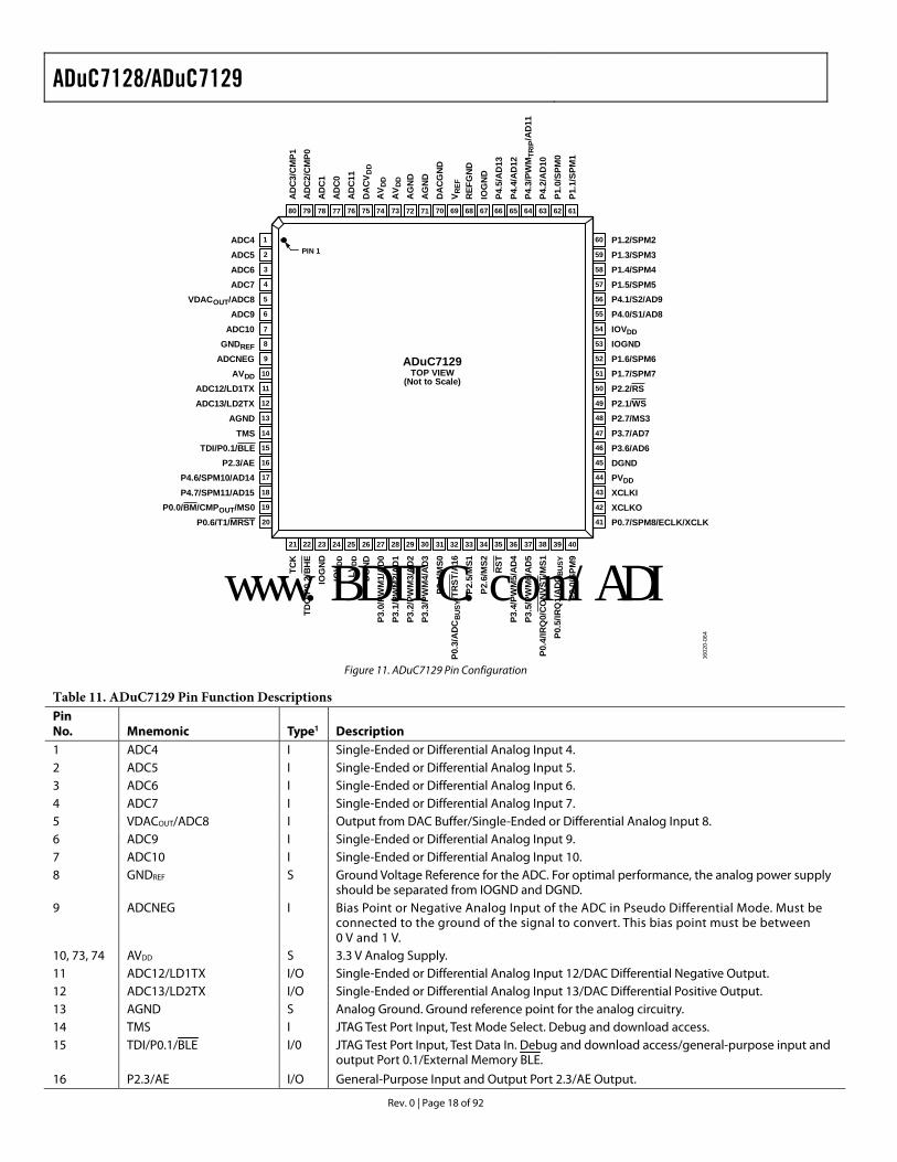
PIN CONFIGURATION AND FUNCTION DESCRIPTIONS
PIN 1INDICATOR
17 18 19 20 21 22 23 24 25 26 27 28 29 30 31 32
TCK
TDO
IOG
ND
IOV D
DLV
DD
DG
ND
P3.0
/PW
M1
P3.1
/PW
M2
P3.2
/PW
M3
P3.3
/PW
M4
P0.3
/AD
CB
USY
/TR
STR
STP3
.4/P
WM
5P3
.5/P
WM
6P0
.4/IR
Q0/
CO
NVS
TP0
.5/IR
Q1/
AD
CB
USY
64 63 62 61 60 59 58 57 56 55 54 53 52 51 50 49
AD
C4
AD
C3/
CM
P1A
DC
2/C
MP0
AD
C1
AD
C0
DA
CV
DD
AV D
DA
GN
DD
AC
GN
DV R
EFP4
.5P4
.4P4
.3/P
WM
TRIP
P4.2
P1.0
/SPM
0P1
.1/S
PM1
123456789
10111213141516
ADC5VDACOUT
ADC9ADC10
GNDREFADCNEG
AVDDADC12/LD1TXADC13/LD2TX
AGNDTMSTDI
P4.6/SPM10P4.7/SPM11
P0.0/BM/CMPOUTP0.6/T1/MRST
P1.2/SPM2P1.3/SPM3P1.4/SPM4P1.5/SPM5P4.1/S2P4.0/S1IOVDDIOGNDP1.6/SPM6P1.7/SPM7DGNDPVDDXCLKIXCLKOP0.7/SPM8/ECLK/XCLKP2.0/SPM9
48474645444342414039383736353433
ADuC7128TOP VIEW
(Not to Scale)
0602
0-06
3
Figure 10. ADuC7128 Pin Configuration
Table 10. ADuC7128 Pin Function Descriptions Pin No. Mnemonic Type1 Description 1 ADC5 I Single-Ended or Differential Analog Input 5/Line Driver Input. 2 VDACOUT O Output from DAC Buffer. 3 ADC9 I Single-Ended or Differential Analog Input 9. 4 ADC10 I Single-Ended or Differential Analog Input 10. 5 GNDREF S Ground Voltage Reference for the ADC. For optimal performance, the analog power supply
should be separated from IOGND and DGND. 6 ADCNEG I Bias Point or Negative Analog Input of the ADC in Pseudo Differential Mode. Must be
connected to the ground of the signal to convert. This bias point must be between 0 V and 1 V.
7, 58 AVDD S Analog Power. 8 ADC12/LD1TX I/O Single-Ended or Differential Analog Input 12/DAC Differential Negative Output. 9 ADC13/LD2TX I/O Single-Ended or Differential Analog Input 13/DAC Differential Positive Output. 10, 57 AGND S Analog Ground. Ground reference point for the analog circuitry. 11 TMS I JTAG Test Port Input, Test Mode Select. Debug and download access. 12 TDI I JTAG Test Port Input, Test Data In. Debug and download access. 13 P4.6/SPM10 I/O General-Purpose Input and Output Port 4.6/Serial Port Mux Pin 10. 14 P4.7/SPM11 I/O General-Purpose Input and Output Port 4.7/Serial Port Mux Pin 11. 15 P0.0/BM/CMPOUT I/O General-Purpose Input and Output Port 0.0/Boot Mode. The ADuC7128 enters download
mode if BM is low at reset and executes code if BM is pulled high at reset through a 1 kΩ resistor/voltage comparator output.
16 P0.6/T1/MRST O General-Purpose Output Port 0.6/Timer1 Input/Power-On Reset Output.
17 TCK I JTAG Test Port Input, Test Clock. Debug and download access. 18 TDO O JTAG Test Port Output, Test Data Out. Debug and download access. 19, 41 IOGND S Ground for GPIO. Typically connected to DGND. 20, 42 IOVDD S 3.3 V Supply for GPIO and Input of the On-Chip Voltage Regulator.
www.BDTIC.com/ADI
ADuC7128/ADuC7129
Rev. 0 | Page 17 of 92
Pin No. Mnemonic Type1 Description 21 LVDD S 2.5 V Output of the On-Chip Voltage Regulator. Must be connected to a 0.47 μF capacitor
to DGND. 22 DGND S Ground for Core Logic. 23 P3.0/PWM1 I/O General-Purpose Input and Output Port 3.0/PWM1 Output. 24 P3.1/PWM2 I/O General-Purpose Input and Output Port 3.1/PWM2 Output. 25 P3.2/PWM3 I/O General-Purpose Input and Output Port 3.2/PWM3 Output. 26 P3.3/PWM4 I/O General-Purpose Input and Output Port 3.3/PWM4 Output. 27 P0.3/ADCBUSY/TRST I/O General-Purpose Input and Output Port 3.3/ADCBUSY Signal/JTAG Test Port Input, Test Reset.
Debug and download access. 28 RST I Reset Input (Active Low).
29 P3.4/PWM5 I/O General-Purpose Input and Output Port 3.4/PWM5 Output. 30 P3.5/PWM6 I/O General-Purpose Input and Output Port 3.5/PWM6 Output. 31 P0.4/IRQ0/CONVST I/O General-Purpose Input and Output Port 0.5/External Interrupt Request 0, Active High/Start
Conversion Input Signal for ADC. 32 P0.5/IRQ1/ADCBUSY I/O General-Purpose Input and Output Port 0.6/External Interrupt Request 1, Active High/ADCBUSY
Signal. 33 P2.0/SPM9 I/O General-Purpose Input and Output Port 2.0/Serial Port Mux Pin 9. 34 P0.7/SPM8/ECLK/XCLK I/O General-Purpose Input and Output Port 0.7/Serial Port Mux Pin 8/Output for the External
Clock Signal/Input to the Internal Clock Generator Circuits. 35 XCLKO O Output from the Crystal Oscillator Inverter. 36 XCLKI I Input to the Crystal Oscillator Inverter and Input to the Internal Clock Generator Circuits. 37 PVDD S 2.5 V PLL Supply. Must be connected to a 0.1 μF capacitor to DGND. Should be connected to
2.5 V LDO output. 38 DGND S Ground for PLL. 39 P1.7/SPM7 I/O General-Purpose Input and Output Port 1.7/Serial Port Mux Pin 7. 40 P1.6/SPM6 I/O General-Purpose Input and Output Port 1.6/Serial Port Mux Pin 6. 43 P4.0/S1 I/O General-Purpose Input and Output Port 4.0/Quadrature Input 1. 44 P4.1/S2 I/O General-Purpose Input and Output Port 4.1/Quadrature Input 2. 45 P1.5/SPM5 I/O General-Purpose Input and Output Port 1.5/Serial Port Mux Pin 5. 46 P1.4/SPM4 I/O General-Purpose Input and Output Port 1.4/Serial Port Mux Pin 4. 47 P1.3/SPM3 I/O General-Purpose Input and Output Port 1.3/Serial Port Mux Pin 3. 48 P1.2/SPM2 I/O General-Purpose Input and Output Port 1.2/Serial Port Mux Pin 2. 49 P1.1/SPM1 I/O General-Purpose Input and Output Port 1.1/Serial Port Mux Pin 1. 50 P1.0/SPM0 I/O General-Purpose Input and Output Port 1.0/Serial Port Mux Pin 0. 51 P4.2 I/O General-Purpose Input and Output Port 4.2. 52 P4.3/ PWMTRIP I/O General-Purpose Input and Output Port 4.3/PWM Safety Cutoff. 53 P4.4 I/O General-Purpose Input and Output Port 4.4. 54 P4.5 I/O General-Purpose Input and Output Port 4.5. 55 VREF I/O 2.5 V Internal Voltage Reference. Must be connected to a 0.47 μF capacitor when using the
internal reference. 56 DACGND S Ground for the DAC. Typically connected to AGND. 59 DACVDD S Power Supply for the DAC. This must be supplied with 2.5 V. This can be connected to the LDO
output. 60 ADC0 I Single-Ended or Differential Analog Input 0. 61 ADC1 I Single-Ended or Differential Analog Input 1. 62 ADC2/CMP0 I Single-Ended or Differential Analog Input 2/Comparator Positive Input. 63 ADC3/CMP1 I Single-Ended or Differential Analog Input 3/Comparator Negative Input. 64 ADC4 I Single-Ended or Differential Analog Input 4. 1 I = input, O = output, S = supply.
www.BDTIC.com/ADI
ADuC7128/ADuC7129
Rev. 0 | Page 18 of 92
0602
0-06
4
2ADC53ADC64ADC7
7ADC10
6ADC9
5VDACOUT/ADC8
1ADC4
8GNDREF9ADCNEG
10AVDD
12ADC13/LD2TX13AGND14TMS15TDI/P0.1/BLE16P2.3/AE17P4.6/SPM10/AD1418P4.7/SPM11/AD1519P0.0/BM/CMPOUT/MS020P0.6/T1/MRST
11ADC12/LD1TX
59
58
57
54
55
56
60
53
52
P1.3/SPM3P1.4/SPM4P1.5/SPM5
IOVDD
P4.0/S1/AD8P4.1/S2/AD9
P1.2/SPM2
IOGNDP1.6/SPM6
51 P1.7/SPM7
49 P2.1/WS48 P2.7/MS347 P3.7/AD746 P3.6/AD645 DGND44 PVDD43 XCLKI42 XCLKO41 P0.7/SPM8/ECLK/XCLK
50 P2.2/RS
21
TCK
22
TDO
/P0.
2/B
HE
23
IOG
ND
24
IOV D
D
25
LVD
D
26
DG
ND
27
P3.0
/PW
M1/
AD
0
28
P3.1
/PW
M2/
AD
1
29
P3.2
/PW
M3/
AD
2
30
P3.3
/PW
M4/
AD
3
31
P2.4
/MS0
32
P0.3
/AD
CB
USY
/TR
ST/A
16
33
P2.5
/MS1
34
P2.6
/MS2
35
RST
36
P3.4
/PW
M5/
AD
4
37
P3.5
/PW
M6/
AD
5
38P0
.4/IR
Q0/
CO
NVS
T/M
S139
P0.5
/IRQ
1/A
DC
BU
SY
40
P2.0
/SPM
9
80
AD
C3/
CM
P1
79
AD
C2/
CM
P0
78
AD
C1
77
AD
C0
76
AD
C11
75
DA
CV
DD
74
AV D
D
73
AV D
D
72
AG
ND
71
AG
ND
70
DA
CG
ND
69
V REF
68
REF
GN
D
67
IOG
ND
66
P4.5
/AD
13
65
P4.4
/AD
12
64
P4.3
/PW
MTR
IP/A
D11
63
P4.2
/AD
10
62
P1.0
/SPM
0
61
P1.1
/SPM
1
PIN 1
ADuC7129TOP VIEW
(Not to Scale)
Figure 11. ADuC7129 Pin Configuration
Table 11. ADuC7129 Pin Function Descriptions Pin No. Mnemonic Type1 Description 1 ADC4 I Single-Ended or Differential Analog Input 4. 2 ADC5 I Single-Ended or Differential Analog Input 5. 3 ADC6 I Single-Ended or Differential Analog Input 6. 4 ADC7 I Single-Ended or Differential Analog Input 7. 5 VDACOUT/ADC8 I Output from DAC Buffer/Single-Ended or Differential Analog Input 8. 6 ADC9 I Single-Ended or Differential Analog Input 9. 7 ADC10 I Single-Ended or Differential Analog Input 10. 8 GNDREF S Ground Voltage Reference for the ADC. For optimal performance, the analog power supply
should be separated from IOGND and DGND. 9 ADCNEG I Bias Point or Negative Analog Input of the ADC in Pseudo Differential Mode. Must be
connected to the ground of the signal to convert. This bias point must be between 0 V and 1 V.
10, 73, 74 AVDD S 3.3 V Analog Supply. 11 ADC12/LD1TX I/O Single-Ended or Differential Analog Input 12/DAC Differential Negative Output. 12 ADC13/LD2TX I/O Single-Ended or Differential Analog Input 13/DAC Differential Positive Output. 13 AGND S Analog Ground. Ground reference point for the analog circuitry. 14 TMS I JTAG Test Port Input, Test Mode Select. Debug and download access. 15 TDI/P0.1/BLE I/0 JTAG Test Port Input, Test Data In. Debug and download access/general-purpose input and
output Port 0.1/External Memory BLE.
16 P2.3/AE I/O General-Purpose Input and Output Port 2.3/AE Output.
www.BDTIC.com/ADI
ADuC7128/ADuC7129
Rev. 0 | Page 19 of 92
Pin No. Mnemonic Type1 Description 17 P4.6/SPM10/AD14 I/O General-Purpose Input and Output Port 4.6/Serial Port Mux Pin 10/External Memory AD14. 18 P4.7/SPM11/AD15 I/O General-Purpose Input and Output Port 4.7/Serial Port Mux Pin 11/External Memory AD15. 19 P0.0/BM/CMPOUT/MS0 I/O General-Purpose Input and Output Port 0.0 /Boot Mode. The ADuC7129 enters download
mode if BM is low at reset and executes code if BM is pulled high at reset through a 1 kΩ resistor/voltage comparator output/external memory MS0.
20 P0.6/T1/MRST O General-Purpose Output Port 0.6/Timer1 Input/Power-On Reset Output/External Memory AE.
21 TCK I JTAG Test Port Input, Test Clock. Debug and download access. 22 TDO/P0.2/BHE O JTAG Test Port Output, Test Data Out. Debug and download access/general-purpose input
and output Port 0.2/External Memory BHE.
23, 53, 67 IOGND S Ground for GPIO. Typically connected to DGND. 24, 54 IOVDD S 3.3 V Supply for GPIO and Input of the On-Chip Voltage Regulator. 25 LVDD S 2.5 V Output of the On-Chip Voltage Regulator. Must be connected to a 0.47 μF capacitor
to DGND. 26 DGND S Ground for Core Logic. 27 P3.0/PWM1/AD0 I/O General-Purpose Input and Output Port 3.0/PWM1 Output/External Memory AD0. 28 P3.1/PWM2/AD1 I/O General-Purpose Input and Output Port 3.1/PWM2 Output/External Memory AD1. 29 P3.2/PWM3/AD2 I/O General-Purpose Input and Output Port 3.2/PWM3 Output/External Memory AD2. 30 P3.3/PWM4/AD3 I/O General-Purpose Input and Output Port 3.3/PWM4 Output//External Memory AD3. 31 P2.4/MS0 I/O General-Purpose Input and Output Port 2.4/Memory Select 0. 32 P0.3/ADCBUSY/TRST/A16 I/O General-Purpose Input and Output Port 3.3/ADCBUSY Signal/JTAG Test Port Input, Test Reset.
Debug and download access/External Memory A16. 33 P2.5/MS1 I/O General-Purpose Input and Output Port 2.5/Memory Select 1. 34 P2.6/MS2 I/O General-Purpose Input and Output Port 2.6/Memory Select 2. 35 RST I Reset Input (Active Low).
36 P3.4/PWM5/AD4 I/O General-Purpose Input and Output Port 3.4/PWM5 Output/External Memory AD4. 37 P3.5/PWM6/AD5 I/O General-Purpose Input and Output Port 3.5/PWM6 Output/External Memory AD5. 38 P0.4/IRQ0/CONVST/MS1 I/O General-Purpose Input and Output Port 0.5/External Interrupt Request 0, Active High/Start
Conversion Input Signal for ADC/External Memory MS1. 39 P0.5/IRQ1/ADCBUSY I/O General-Purpose Input and Output Port 0.6/External Interrupt Request 1, Active
High/ADCBUSY Signal. 40 P2.0/SPM9 I/O General-Purpose Input and Output Port 2.0/Serial Port Mux Pin 9. 41 P0.7/SPM8/ECLK/XCLK I/O General-Purpose Input and Output Port 0.7/Serial Port Mux Pin 8/Output for the External
Clock Signal/Input to the Internal Clock Generator Circuits. 42 XCLKO O Output from the Crystal Oscillator Inverter. 43 XCLKI I Input to the Crystal Oscillator Inverter and Input to the Internal Clock Generator Circuits. 44 PVDD S 2.5 V PLL Supply. Must be connected to a 0.1 μF capacitor to DGND. Should be connected
to 2.5 V LDO output. 45 DGND S Ground for PLL. 46 P3.6/AD6 I/O General-Purpose Input and Output Port 3.6/External Memory AD6. 47 P3.7/AD7 I/O General-Purpose Input and Output Port 3.7/External Memory AD7. 48 P2.7/MS3 I/O General-Purpose Input and Output Port 2.7/Memory Select 3. 49 P2.1/WS I/O General-Purpose Input and Output Port 2.1/Memory Write Select.
50 P2.2/RS I/O General-Purpose Input and Output Port 2.1/Memory Read Select.
51 P1.7/SPM7 I/O General-Purpose Input and Output Port 1.7/Serial Port Mux Pin 7. 52 P1.6/SPM6 I/O General-Purpose Input and Output Port 1.6/Serial Port Mux Pin 6. 55 P4.0/S1/AD8 I/O General-Purpose Input and Output Port 4.0/Quadrature Input 1/External Memory AD8. 56 P4.1/S2/AD9 I/O General-Purpose Input and Output Port 4.1/Quadrature Input 2/External Memory AD9. 57 P1.5/SPM5 I/O General-Purpose Input and Output Port 1.5/Serial Port Mux Pin 5. 58 P1.4/SPM4 I/O General-Purpose Input and Output Port 1.4/Serial Port Mux Pin 4. 59 P1.3/SPM3 I/O General-Purpose Input and Output Port 1.3/Serial Port Mux Pin 3. 60 P1.2/SPM2 I/O General-Purpose Input and Output Port 1.2/Serial Port Mux Pin 2. 61 P1.1/SPM1 I/O General-Purpose Input and Output Port 1.1/Serial Port Mux Pin 1. 62 P1.0/SPM0 I/O General-Purpose Input and Output Port 1.0/Serial Port Mux Pin 0.
www.BDTIC.com/ADI
ADuC7128/ADuC7129
Rev. 0 | Page 20 of 92
Pin No. Mnemonic Type1 Description 63 P4.2/AD10 I/O General-Purpose Input and Output Port 4.2/External Memory AD10. 64 P4.3/PWMTRIP/AD11 I/O General-Purpose Input and Output Port 4.3/PWM Safety Cutoff/External Memory AD11. 65 P4.4/AD12 I/O General-Purpose Input and Output Port 4.4/External Memory AD12. 66 P4.5/AD13 I/O General-Purpose Input and Output Port 4.5/External Memory AD13. 68 REFGND S Ground for VREF. Typically connected to DGND. 69 VREF I/O 2.5 V Internal Voltage Reference. Must be connected to a 0.47 μF capacitor when using the
internal reference. 70 DACGND S Ground for the DAC. Typically connected to AGND. 71, 72 AGND S Analog Ground. 75 DACVDD S Power Supply for the DAC. This must be supplied with 2.5 V. It can be connected to the LDO
output. 76 ADC11 I Single-Ended or Differential Analog Input 11. 77 ADC0 I Single-Ended or Differential Analog Input 0. 78 ADC1 I Single-Ended or Differential Analog Input 1. 79 ADC2/CMP0 I Single-Ended or Differential Analog Input 2/Comparator Positive Input. 80 ADC3/CMP1 I Single-Ended or Differential Analog Input 3/Comparator Negative Input. 1 I = input, O = output, S = supply.
www.BDTIC.com/ADI
ADuC7128/ADuC7129
Rev. 0 | Page 21 of 92
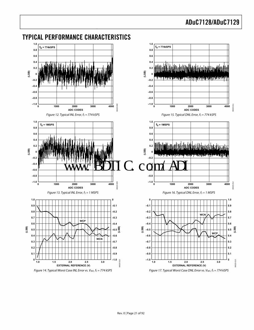
TYPICAL PERFORMANCE CHARACTERISTICS
ADC CODES
(LSB
)
1.0
–1.0
–0.8
–0.6
–0.4
–0.2
0
0.2
0.4
0.6
0.8
0 20001000 3000 4000
fS = 774kSPS
0602
0-00
8
Figure 12. Typical INL Error, fS = 774 kSPS
ADC CODES
(LSB
)
1.0
–1.0
–0.8
–0.6
–0.4
–0.2
0
0.2
0.4
0.6
0.8
0 20001000 3000 4000
fS = 1MSPS
0602
0-00
9
Figure 13. Typical INL Error, fS = 1 MSPS
EXTERNAL REFERENCE (V)
(LSB
)
(LSB
)
1.0
0
0.1
0.2
0.3
0.4
0.5
0.6
0.7
0.8
0.9
0
–0.1
–0.2
–0.3
–0.5
–0.4
–0.6
–0.7
–0.8
–0.9
–1.01.0 1.5 2.0 2.5 3.0
WCN
WCP
0602
0-01
0
Figure 14. Typical Worst Case INL Error vs. VREF, fS = 774 kSPS
ADC CODES
(LSB
)
1.0
–1.0
–0.8
–0.6
–0.4
–0.2
0
0.2
0.4
0.6
0.8
0 20001000 3000 4000
fS = 774kSPS
0602
0-01
1
Figure 15. Typical DNL Error, fS = 774 kSPS
ADC CODES
(LSB
)
1.0
–1.0
–0.8
–0.6
–0.4
–0.2
0
0.2
0.4
0.6
0.8
0 20001000 3000 4000
fS = 1MSPS
0602
0-01
2
Figure 16. Typical DNL Error, fS = 1 MSPS
EXTERNAL REFERENCE (V)
(LSB
)
(LSB
)
0
–1.0
–0.9
–0.8
–0.7
–0.6
–0.5
–0.4
–0.3
–0.2
–0.1
1.0
0.9
0.8
0.7
0.6
0.5
0.4
0.3
0.2
0.1
01.0 1.5 2.0 2.5 3.0
WCN
WCP06
020-
013
Figure 17. Typical Worst Case DNL Error vs. VREF, fS = 774 kSPS
www.BDTIC.com/ADI
ADuC7128/ADuC7129
Rev. 0 | Page 22 of 92
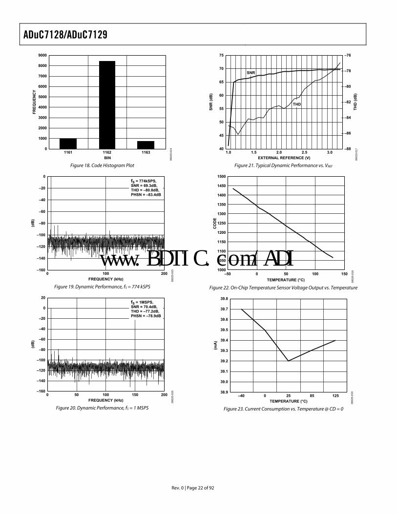
BIN
FREQ
UEN
CY
9000
0
1000
2000
3000
4000
5000
6000
7000
8000
1161 1162 1163
0602
0-01
4
Figure 18. Code Histogram Plot
FREQUENCY (kHz)
(dB
)
0
–160
–140
–120
–100
–80
–60
–40
–20
0 100 200
fS = 774kSPS,SNR = 69.3dB,THD = –80.8dB,PHSN = –83.4dB
0602
0-01
5
Figure 19. Dynamic Performance, fS = 774 kSPS
FREQUENCY (kHz)
(dB
)
20
0
–160
–140
–120
–100
–80
–60
–40
–20
0 110050 20050
fS = 1MSPS,SNR = 70.4dB,THD = –77.2dB,PHSN = –78.9dB
0602
0-01
6
Figure 20. Dynamic Performance, fS = 1 MSPS
EXTERNAL REFERENCE (V)
SNR
(dB
)
THD
(dB
)
75
40
45
50
55
60
65
70
–76
–88
–86
–84
–82
–80
–78
1.0 1.5 2.0 2.5 3.0
SNR
THD
0602
0-01
7
Figure 21. Typical Dynamic Performance vs. VREF
TEMPERATURE (°C)
CO
DE
–50 0 50 1001000
1500
1450
1400
1350
1300
1250
1200
1150
1100
1050
150
0602
0-01
8
Figure 22. On-Chip Temperature Sensor Voltage Output vs. Temperature
TEMPERATURE (°C)
(mA
)
39.8
39.7
38.9
39.0
39.1
39.2
39.3
39.4
39.5
39.6
–40 25 850 125
0602
0-01
9
Figure 23. Current Consumption vs. Temperature @ CD = 0
www.BDTIC.com/ADI
ADuC7128/ADuC7129
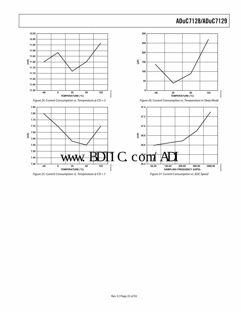
Rev. 0 | Page 23 of 92
25TEMPERATURE (°C)
(mA
)
12.05
11.95
12.00
11.55
11.60
11.65
11.70
11.75
11.80
11.85
11.90
–40 25 850 1
0602
0-02
0
Figure 24. Current Consumption vs. Temperature @ CD = 3
TEMPERATURE (°C)
(mA
)
7.85
7.75
7.80
7.40
7.45
7.50
7.55
7.60
7.65
7.70
–40 25 850 125
0602
0-02
1
Figure 25. Current Consumption vs. Temperature @ CD = 7
TEMPERATURE (°C)
(µA
)
300
0–40 125
250
200
150
100
50
25 85
0602
0-02
2
Figure 26. Current Consumption vs. Temperature in Sleep Mode
SAMPLING FREQUENCY (kSPS)
(mA
)
37.4
37.2
37.0
36.8
36.6
36.4
36.262.25 250.00 500.00125.00 1000.00
0602
0-02
3
Figure 27. Current Consumption vs. ADC Speed
www.BDTIC.com/ADI
ADuC7128/ADuC7129
Rev. 0 | Page 24 of 92
TERMINOLOGY ADC SPECIFICATIONS Integral Nonlinearity The maximum deviation of any code from a straight line passing through the endpoints of the ADC transfer function. The endpoints of the transfer function are zero scale, a point ½ LSB below the first code transition and full scale, a point ½ LSB above the last code transition.
Differential Nonlinearity The difference between the measured and the ideal 1 LSB change between any two adjacent codes in the ADC.
Offset Error The deviation of the first code transition (0000 . . . 000) to (0000 . . . 001) from the ideal, that is, +½ LSB.
Gain Error The deviation of the last code transition from the ideal AIN voltage (full scale − 1.5 LSB) after the offset error has been adjusted out.
Signal to (Noise + Distortion) Ratio The measured ratio of signal to (noise + distortion) at the output of the ADC. The signal is the rms amplitude of the fundamental. Noise is the rms sum of all nonfundamental signals up to half the sampling frequency (fS/2), excluding dc. The ratio is dependent on the number of quantization levels in the digitization process; the more levels, the smaller the quantization noise.
The theoretical signal to (noise + distortion) ratio for an ideal N-bit converter with a sine wave input is given by
Signal to (Noise + Distortion) = (6.02 N + 1.76) dB
Thus, for a 12-bit converter, this is 74 dB.
Total Harmonic Distortion The ratio of the rms sum of the harmonics to the fundamental.
DAC SPECIFICATIONS Relative Accuracy Otherwise known as endpoint linearity, relative accuracy is a measure of the maximum deviation from a straight line passing through the endpoints of the DAC transfer function. It is measured after adjusting for zero error and full-scale error.
Voltage Output Settling Time The amount of time it takes for the output to settle to within a 1 LSB level for a full-scale input change.
www.BDTIC.com/ADI
ADuC7128/ADuC7129
Rev. 0 | Page 25 of 92
OVERVIEW OF THE ARM7TDMI CORE The ARM7 core is a 32-bit reduced instruction set computer (RISC). It uses a single 32-bit bus for instruction and data. The length of the data can be 8 bits, 16 bits, or 32 bits. The length of the instruction word is 32 bits.
The ARM7TDMI is an ARM7 core with the following four additional features:
• T, support for the Thumb® (16-bit) instruction set • D, support for debug • M, support for long multiplications • I, includes the embedded ICE module to support
embedded system debugging
THUMB MODE (T) An ARM® instruction is 32-bits long. The ARM7TDMI processor supports a second instruction set that has been compressed into 16-bits, called the Thumb instruction set. Faster execution from 16-bit memory and greater code density can usually be achieved by using the Thumb instruction set instead of the ARM instruction set, which makes the ARM7TDMI core particularly suitable for embedded applications.
However, the Thumb mode has two limitations:
• Thumb code typically requires more instructions for the same job. As a result, ARM code is usually best for maximizing the performance of the time-critical code.
• The Thumb instruction set does not include some of the instructions needed for exception handling, which auto-matically switches the core to ARM code for exception handling.
See the ARM7TDMI user guide for details on the core architecture, the programming model, and both the ARM and Thumb instruction sets.
LONG MULTIPLY (M) The ARM7TDMI instruction set includes four extra instruc-tions that perform 32-bit by 32-bit multiplication with 64-bit result, and 32-bit by 32-bit multiplication-accumulation (MAC) with 64-bit result. This result is achieved in fewer cycles than required on a standard ARM7 core.
EMBEDDEDICE (I) EmbeddedICE provides integrated on-chip support for the core. The EmbeddedICE module contains the breakpoint and watch-point registers that allow code to be halted for debugging purposes. These registers are controlled through the JTAG test port.
When a breakpoint or watchpoint is encountered, the processor halts and enters debug state. Once in a debug state, the processor registers can be inspected, as well as the Flash/EE, the SRAM, and the memory mapped registers.
EXCEPTIONS ARM supports five types of exceptions and a privileged processing mode for each type. The five types of exceptions are
• Normal interrupt or IRQ. This is provided to service general-purpose interrupt handling of internal and external events.
• Fast interrupt or FIQ. This is provided to service data transfer or communication channel with low latency. FIQ has priority over IRQ.
• Memory abort. • Attempted execution of an undefined instruction. • Software interrupt instruction (SWI). This can be used to
make a call to an operating system.
Typically, the programmer defines interrupt as IRQ, but for higher priority interrupt, that is, faster response time, the programmer can define interrupt as FIQ.
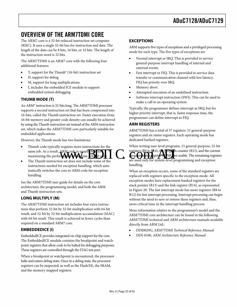
ARM REGISTERS ARM7TDMI has a total of 37 registers: 31 general-purpose registers and six status registers. Each operating mode has dedicated banked registers.
When writing user-level programs, 15 general-purpose, 32-bit registers (R0 to R14), the program counter (R15), and the current program status register (CPSR) are usable. The remaining registers are used only for system-level programming and exception handling.
When an exception occurs, some of the standard registers are replaced with registers specific to the exception mode. All exception modes have replacement banked registers for the stack pointer (R13) and the link register (R14), as represented in Figure 28. The fast interrupt mode has more registers (R8 to R12) for fast interrupt processing. Interrupt processing can begin without the need to save or restore these registers and, thus, saves critical time in the interrupt handling process.
More information relative to the programmer’s model and the ARM7TDMI core architecture can be found in the following ARM7TDMI technical and ARM architecture manuals available directly from ARM Ltd.: • DDI0029G, ARM7TDMI Technical Reference Manual • DDI-0100, ARM Architecture Reference Manual
www.BDTIC.com/ADI
ADuC7128/ADuC7129
Rev. 0 | Page 26 of 92
USABLE IN USER MODE
SYSTEM MODES ONLY
SPSR_UNDSPSR_IRQSPSR_ABTSPSR_SVC
R8_FIQR9_FIQ
R10_FIQR11_FIQR12_FIQR13_FIQR14_FIQ
R13_UNDR14_UND
R0R1R2R3R4R5R6R7R8R9
R10R11R12R13R14
R15 (PC)
R13_IRQR14_IRQ
R13_ABTR14_ABT
R13_SVCR14_SVC
SPSR_FIQCPSR
USER MODEFIQ
MODESVC
MODEABORTMODE
IRQMODE
UNDEFINEDMODE 06
020-
024
Figure 28. Register Organization
INTERRUPT LATENCY The worst case latency for an FIQ consists of the following:
• The longest time the request can take to pass through the synchronizer
• The time for the longest instruction to complete (the longest instruction is an LDM) that loads all the registers, including the PC
• The time for the data abort entry • The time for FIQ entry
At the end of this time, the ARM7TDMI executes the instruction at Address 0x1C (FIQ interrupt vector address). The maximum total time is 50 processor cycles, which is just under 1.2 μs in a system using a continuous 41.78 MHz processor clock.
The maximum IRQ latency calculation is similar, but it must allow for the fact that FIQ has higher priority and could delay entry into the IRQ handling routine for an arbitrary length of time. This time can be reduced to 42 cycles if the LDM command is not used; some compilers have an option to compile without using this command. Another option is to run the part in Thumb mode, where the time is reduced to 22 cycles.
The minimum latency for FIQ or IRQ interrupts is five cycles. It consists of the shortest time the request can take through the synchronizer plus the time to enter the exception mode.
Note that the ARM7TDMI always runs in ARM (32-bit) mode when in privileged modes, that is, when executing interrupt service routines.
www.BDTIC.com/ADI
ADuC7128/ADuC7129
Rev. 0 | Page 27 of 92
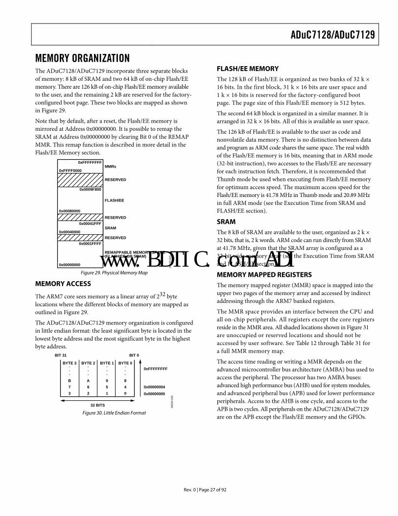
MEMORY ORGANIZATIONThe ADuC7128/ADuC7129 incorporate three separate blocks of memory: 8 kB of SRAM and two 64 kB of on-chip Flash/EE memory. There are 126 kB of on-chip Flash/EE memory available to the user, and the remaining 2 kB are reserved for the factory-configured boot page. These two blocks are mapped as shown in Figure 29.
Note that by default, after a reset, the Flash/EE memory is mirrored at Address 0x00000000. It is possible to remap the SRAM at Address 0x00000000 by clearing Bit 0 of the REMAP MMR. This remap function is described in more detail in the Flash/EE Memory section.
RESERVED
0x00080000
FLASH/EE
RESERVED0x00041FFF
0x00040000SRAM
0xFFFF0000
0xFFFFFFFFMMRs
0x0001FFFF
0x00000000
0x0009F800
RESERVED
REMAPPABLE MEMORY SPACE(FLASH/EE OR SRAM)
0602
0-02
5
Figure 29. Physical Memory Map
MEMORY ACCESS
The ARM7 core sees memory as a linear array of 232 byte locations where the different blocks of memory are mapped as outlined in Figure 29.
The ADuC7128/ADuC7129 memory organization is configured in little endian format: the least significant byte is located in the lowest byte address and the most significant byte in the highest byte address.
BIT 31
BYTE 2
A62
.
.
.
BYTE 3
B73
.
.
.
BYTE 1
951
.
.
.
BYTE 0
840
.
.
.
BIT 0
32 BITS
0xFFFFFFFF
0x00000004
0x00000000
0602
0-02
6
Figure 30. Little Endian Format
FLASH/EE MEMORY The 128 kB of Flash/EE is organized as two banks of 32 k × 16 bits. In the first block, 31 k × 16 bits are user space and 1 k × 16 bits is reserved for the factory-configured boot page. The page size of this Flash/EE memory is 512 bytes.
The second 64 kB block is organized in a similar manner. It is arranged in 32 k × 16 bits. All of this is available as user space.
The 126 kB of Flash/EE is available to the user as code and nonvolatile data memory. There is no distinction between data and program as ARM code shares the same space. The real width of the Flash/EE memory is 16 bits, meaning that in ARM mode (32-bit instruction), two accesses to the Flash/EE are necessary for each instruction fetch. Therefore, it is recommended that Thumb mode be used when executing from Flash/EE memory for optimum access speed. The maximum access speed for the Flash/EE memory is 41.78 MHz in Thumb mode and 20.89 MHz in full ARM mode (see the Execution Time from SRAM and FLASH/EE section).
SRAM The 8 kB of SRAM are available to the user, organized as 2 k × 32 bits, that is, 2 k words. ARM code can run directly from SRAM at 41.78 MHz, given that the SRAM array is configured as a 32-bit wide memory array (see the Execution Time from SRAM and FLASH/EE section).
MEMORY MAPPED REGISTERS The memory mapped register (MMR) space is mapped into the upper two pages of the memory array and accessed by indirect addressing through the ARM7 banked registers.
The MMR space provides an interface between the CPU and all on-chip peripherals. All registers except the core registers reside in the MMR area. All shaded locations shown in Figure 31 are unoccupied or reserved locations and should not be accessed by user software. See Table 12 through Table 31 for a full MMR memory map.
The access time reading or writing a MMR depends on the advanced microcontroller bus architecture (AMBA) bus used to access the peripheral. The processor has two AMBA buses: advanced high performance bus (AHB) used for system modules, and advanced peripheral bus (APB) used for lower performance peripherals. Access to the AHB is one cycle, and access to the APB is two cycles. All peripherals on the ADuC7128/ADuC7129 are on the APB except the Flash/EE memory and the GPIOs.
www.BDTIC.com/ADI

ADuC7128/ADuC7129
Rev. 0 | Page 28 of 92
SPI
0xFFFF0900
0xFFFF0848
0xFFFF0800
0xFFFF076C
0xFFFF0740
0xFFFF0948
0xFFFF0B00
0xFFFF0A00
0xFFFF0A14
UART00xFFFF072C
0xFFFF0700
UART1
I2C0
I2C1
FLASH CONTROLINTERFACE 0
0xFFFFFFFF
0xFFFF0B54
0xFFFF0C00
0xFFFF0C30EXTERNAL MEMORY
PLA
0xFFFF0D00
0xFFFF0D70GPIO
0xFFFF0E00
0xFFFF0E28
FLASH CONTROLINTERFACE 1
0xFFFF0E80
0xFFFF0EA8
QEN0xFFFF0F00
0xFFFF0F18
PWM0xFFFF0F80
0xFFFF0FBC
INTERRUPTCONTROLLER
REMAP ANDSYSTEM CONTROL
DDS
DAC
ADC
BANDGAPREFERENCE
POWER SUPPLYMONITOR
TIMER 0
GENERAL PURPOSETIMER 4
WATCHDOGTIMER
GENERAL PURPOSETIMER
WAKEUPTIMER
0xFFFF0000
0xFFFF0110
0xFFFF0320
0xFFFF0318
0xFFFF0300
0xFFFF0240
0xFFFF0200
0xFFFF0670
0xFFFF06BC
0xFFFF0690
0xFFFF0688
0xFFFF0500
0xFFFF0544
0xFFFF04A8
0xFFFF0480
0xFFFF0334
0xFFFF0448
0xFFFF0440
0xFFFF0434
0xFFFF0400
0xFFFF0340
0xFFFF0350
0xFFFF0360
0xFFFF0370
PLL ANDOSCILLATOR
CONTROL
0xFFFF0380
0xFFFF039406
020-
027
Figure 31. Memory Mapped Registers
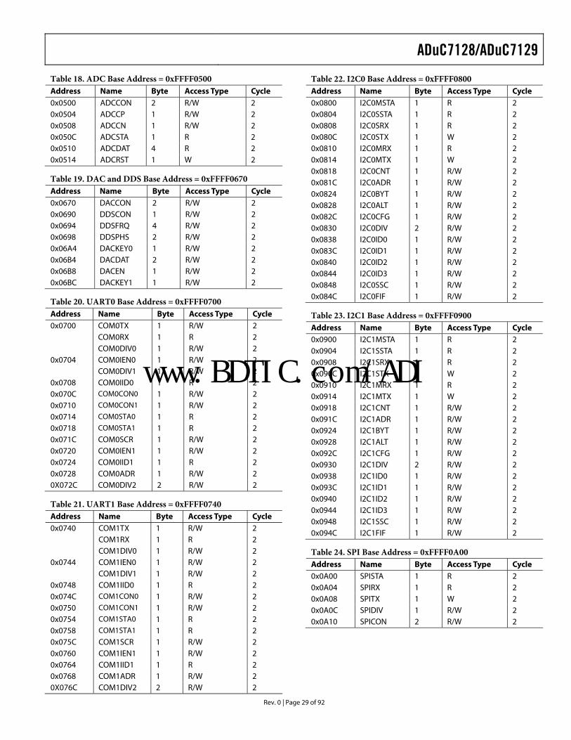
COMPLETE MMR LISTING Note that the Access Type column corresponds to the access time reading or writing an MMR. It depends on the AMBA bus used to access the peripheral. The processor has two AMBA buses: the AHB (advanced high performance bus) used for system modules and the APB (advanced peripheral bus) used for lower performance peripherals.
Table 12. IRQ Base Address = 0xFFFF0000 Address Name Byte Access Type Cycle 0x0000 IRQSTA 4 R 1 0x0004 IRQSIG 4 R 1 0x0008 IRQEN 4 R/W 1 0x000C IRQCLR 4 W 1 0x0010 SWICFG 4 W 1 0x0100 FIQSTA 4 R 1 0x0104 FIQSIG 4 R 1 0x0108 FIQEN 4 R/W 1 0x010C FIQCLR 4 W 1
Table 13. System Control Base Address = 0xFFFF0200 Address Name Byte Access Type Cycle 0x0220 REMAP 1 R/W 1 0x0230 RSTSTA 1 R 1 0x0234 RSTCLR 1 W 1
Table 14. Timer Base Address = 0xFFFF0300 Address Name Byte Access Type Cycle 0x0300 T0LD 2 R/W 2 0x0304 T0VAL0 2 R 2 0x0308 T0VAL1 4 R 2 0x030C T0CON 4 R/W 2 0x0310 T0ICLR 1 W 2 0x0314 T0CAP 2 R 2 0x0320 T1LD 4 R/W 2 0x0324 T1VAL 4 R 2 0x0328 T1CON 4 R/W 2 0x032C T1ICLR 1 W 2 0x0330 T1CAP 4 R 2 0x0340 T2LD 4 R/W 2 0x0344 T2VAL 4 R 2 0x0348 T2CON 4 R/W 2 0x034C T2ICLR 1 W 2 0x0360 T3LD 2 R/W 2 0x0364 T3VAL 2 R 2 0x0368 T3CON 2 R/W 2 0x036C T3ICLR 1 W 2 0x0380 T4LD 4 R/W 2 0x0384 T4VAL 4 R 2 0x0388 T4CON 4 R/W 2 0x038C T4ICLR 1 W 2 0x0390 T4CAP 4 R 2
Table 15. PLL Base Address = 0xFFFF0400 Address Name Byte Access Type Cycle 0x0404 POWKEY1 2 W 2 0x0408 POWCON 2 R/W 2 0x040C POWKEY2 2 W 2 0x0410 PLLKEY1 2 W 2 0x0414 PLLCON 2 R/W 2 0x0418 PLLKEY2 2 W 2
Table 16. PSM Base Address = 0xFFFF0440 Address Name Byte Access Type Cycle 0x0440 PSMCON 2 R/W 2 0x0444 CMPCON 2 R/W 2
Table 17. Reference Base Address = 0xFFFF0480 Address Name Byte Access Type Cycle 0x048C REFCON 1 R/W 2
www.BDTIC.com/ADI
ADuC7128/ADuC7129
Rev. 0 | Page 29 of 92
Table 18. ADC Base Address = 0xFFFF0500 Address Name Byte Access Type Cycle 0x0500 ADCCON 2 R/W 2 0x0504 ADCCP 1 R/W 2 0x0508 ADCCN 1 R/W 2 0x050C ADCSTA 1 R 2 0x0510 ADCDAT 4 R 2 0x0514 ADCRST 1 W 2
Table 19. DAC and DDS Base Address = 0xFFFF0670 Address Name Byte Access Type Cycle 0x0670 DACCON 2 R/W 2 0x0690 DDSCON 1 R/W 2 0x0694 DDSFRQ 4 R/W 2 0x0698 DDSPHS 2 R/W 2 0x06A4 DACKEY0 1 R/W 2 0x06B4 DACDAT 2 R/W 2 0x06B8 DACEN 1 R/W 2 0x06BC DACKEY1 1 R/W 2
Table 20. UART0 Base Address = 0xFFFF0700 Address Name Byte Access Type Cycle 0x0700 COM0TX 1 R/W 2 COM0RX 1 R 2 COM0DIV0 1 R/W 2 0x0704 COM0IEN0 1 R/W 2 COM0DIV1 1 R/W 2 0x0708 COM0IID0 1 R 2 0x070C COM0CON0 1 R/W 2 0x0710 COM0CON1 1 R/W 2 0x0714 COM0STA0 1 R 2 0x0718 COM0STA1 1 R 2 0x071C COM0SCR 1 R/W 2 0x0720 COM0IEN1 1 R/W 2 0x0724 COM0IID1 1 R 2 0x0728 COM0ADR 1 R/W 2 0X072C COM0DIV2 2 R/W 2
Table 21. UART1 Base Address = 0xFFFF0740 Address Name Byte Access Type Cycle 0x0740 COM1TX 1 R/W 2 COM1RX 1 R 2 COM1DIV0 1 R/W 2 0x0744 COM1IEN0 1 R/W 2 COM1DIV1 1 R/W 2 0x0748 COM1IID0 1 R 2 0x074C COM1CON0 1 R/W 2 0x0750 COM1CON1 1 R/W 2 0x0754 COM1STA0 1 R 2 0x0758 COM1STA1 1 R 2 0x075C COM1SCR 1 R/W 2 0x0760 COM1IEN1 1 R/W 2 0x0764 COM1IID1 1 R 2 0x0768 COM1ADR 1 R/W 2 0X076C COM1DIV2 2 R/W 2
Table 22. I2C0 Base Address = 0xFFFF0800 Address Name Byte Access Type Cycle 0x0800 I2C0MSTA 1 R 2 0x0804 I2C0SSTA 1 R 2 0x0808 I2C0SRX 1 R 2 0x080C I2C0STX 1 W 2 0x0810 I2C0MRX 1 R 2 0x0814 I2C0MTX 1 W 2 0x0818 I2C0CNT 1 R/W 2 0x081C I2C0ADR 1 R/W 2 0x0824 I2C0BYT 1 R/W 2 0x0828 I2C0ALT 1 R/W 2 0x082C I2C0CFG 1 R/W 2 0x0830 I2C0DIV 2 R/W 2 0x0838 I2C0ID0 1 R/W 2 0x083C I2C0ID1 1 R/W 2 0x0840 I2C0ID2 1 R/W 2 0x0844 I2C0ID3 1 R/W 2 0x0848 I2C0SSC 1 R/W 2 0x084C I2C0FIF 1 R/W 2
Table 23. I2C1 Base Address = 0xFFFF0900 Address Name Byte Access Type Cycle 0x0900 I2C1MSTA 1 R 2 0x0904 I2C1SSTA 1 R 2 0x0908 I2C1SRX 1 R 2 0x090C I2C1STX 1 W 2 0x0910 I2C1MRX 1 R 2 0x0914 I2C1MTX 1 W 2 0x0918 I2C1CNT 1 R/W 2 0x091C I2C1ADR 1 R/W 2 0x0924 I2C1BYT 1 R/W 2 0x0928 I2C1ALT 1 R/W 2 0x092C I2C1CFG 1 R/W 2 0x0930 I2C1DIV 2 R/W 2 0x0938 I2C1ID0 1 R/W 2 0x093C I2C1ID1 1 R/W 2 0x0940 I2C1ID2 1 R/W 2 0x0944 I2C1ID3 1 R/W 2 0x0948 I2C1SSC 1 R/W 2 0x094C I2C1FIF 1 R/W 2
Table 24. SPI Base Address = 0xFFFF0A00 Address Name Byte Access Type Cycle 0x0A00 SPISTA 1 R 2 0x0A04 SPIRX 1 R 2 0x0A08 SPITX 1 W 2 0x0A0C SPIDIV 1 R/W 2 0x0A10 SPICON 2 R/W 2
www.BDTIC.com/ADI
ADuC7128/ADuC7129
Rev. 0 | Page 30 of 92
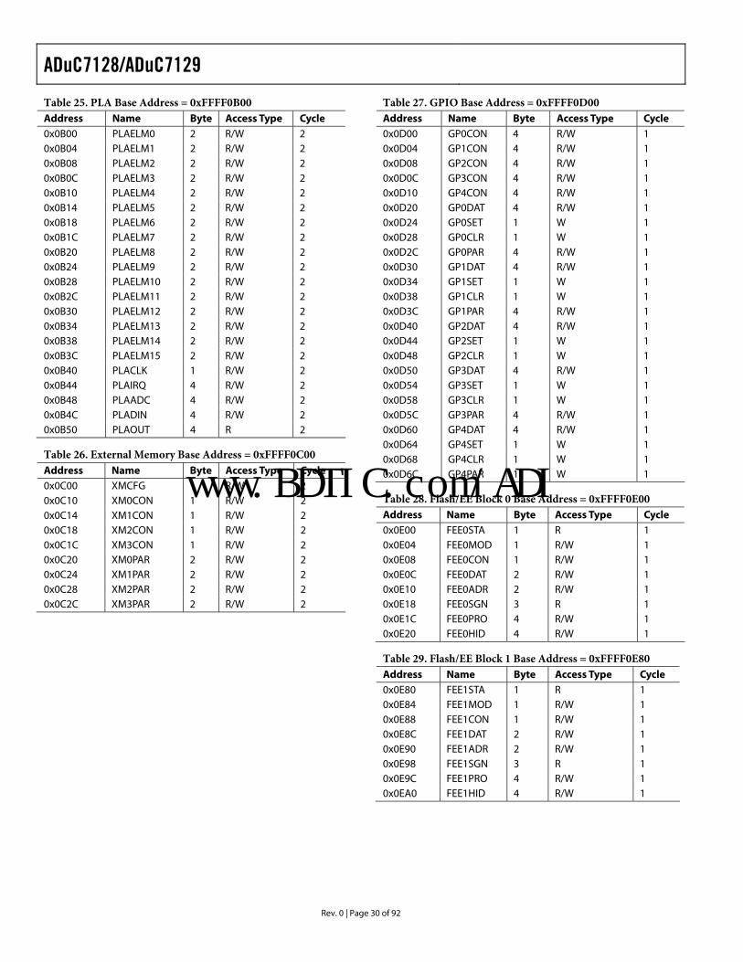
Table 25. PLA Base Address = 0xFFFF0B00 Address Name Byte Access Type Cycle 0x0B00 PLAELM0 2 R/W 2 0x0B04 PLAELM1 2 R/W 2 0x0B08 PLAELM2 2 R/W 2 0x0B0C PLAELM3 2 R/W 2 0x0B10 PLAELM4 2 R/W 2 0x0B14 PLAELM5 2 R/W 2 0x0B18 PLAELM6 2 R/W 2 0x0B1C PLAELM7 2 R/W 2 0x0B20 PLAELM8 2 R/W 2 0x0B24 PLAELM9 2 R/W 2 0x0B28 PLAELM10 2 R/W 2 0x0B2C PLAELM11 2 R/W 2 0x0B30 PLAELM12 2 R/W 2 0x0B34 PLAELM13 2 R/W 2 0x0B38 PLAELM14 2 R/W 2 0x0B3C PLAELM15 2 R/W 2 0x0B40 PLACLK 1 R/W 2 0x0B44 PLAIRQ 4 R/W 2 0x0B48 PLAADC 4 R/W 2 0x0B4C PLADIN 4 R/W 2 0x0B50 PLAOUT 4 R 2
Table 26. External Memory Base Address = 0xFFFF0C00 Address Name Byte Access Type Cycle 0x0C00 XMCFG 1 R/W 2 0x0C10 XM0CON 1 R/W 2 0x0C14 XM1CON 1 R/W 2 0x0C18 XM2CON 1 R/W 2 0x0C1C XM3CON 1 R/W 2 0x0C20 XM0PAR 2 R/W 2 0x0C24 XM1PAR 2 R/W 2 0x0C28 XM2PAR 2 R/W 2 0x0C2C XM3PAR 2 R/W 2
Table 27. GPIO Base Address = 0xFFFF0D00 Address Name Byte Access Type Cycle 0x0D00 GP0CON 4 R/W 1 0x0D04 GP1CON 4 R/W 1 0x0D08 GP2CON 4 R/W 1 0x0D0C GP3CON 4 R/W 1 0x0D10 GP4CON 4 R/W 1 0x0D20 GP0DAT 4 R/W 1 0x0D24 GP0SET 1 W 1 0x0D28 GP0CLR 1 W 1 0x0D2C GP0PAR 4 R/W 1 0x0D30 GP1DAT 4 R/W 1 0x0D34 GP1SET 1 W 1 0x0D38 GP1CLR 1 W 1 0x0D3C GP1PAR 4 R/W 1 0x0D40 GP2DAT 4 R/W 1 0x0D44 GP2SET 1 W 1 0x0D48 GP2CLR 1 W 1 0x0D50 GP3DAT 4 R/W 1 0x0D54 GP3SET 1 W 1 0x0D58 GP3CLR 1 W 1 0x0D5C GP3PAR 4 R/W 1 0x0D60 GP4DAT 4 R/W 1 0x0D64 GP4SET 1 W 1 0x0D68 GP4CLR 1 W 1 0x0D6C GP4PAR 1 W 1
Table 28. Flash/EE Block 0 Base Address = 0xFFFF0E00 Address Name Byte Access Type Cycle 0x0E00 FEE0STA 1 R 1 0x0E04 FEE0MOD 1 R/W 1 0x0E08 FEE0CON 1 R/W 1 0x0E0C FEE0DAT 2 R/W 1 0x0E10 FEE0ADR 2 R/W 1 0x0E18 FEE0SGN 3 R 1 0x0E1C FEE0PRO 4 R/W 1 0x0E20 FEE0HID 4 R/W 1
Table 29. Flash/EE Block 1 Base Address = 0xFFFF0E80 Address Name Byte Access Type Cycle 0x0E80 FEE1STA 1 R 1 0x0E84 FEE1MOD 1 R/W 1 0x0E88 FEE1CON 1 R/W 1 0x0E8C FEE1DAT 2 R/W 1 0x0E90 FEE1ADR 2 R/W 1 0x0E98 FEE1SGN 3 R 1 0x0E9C FEE1PRO 4 R/W 1 0x0EA0 FEE1HID 4 R/W 1
www.BDTIC.com/ADI
ADuC7128/ADuC7129
Rev. 0 | Page 31 of 92
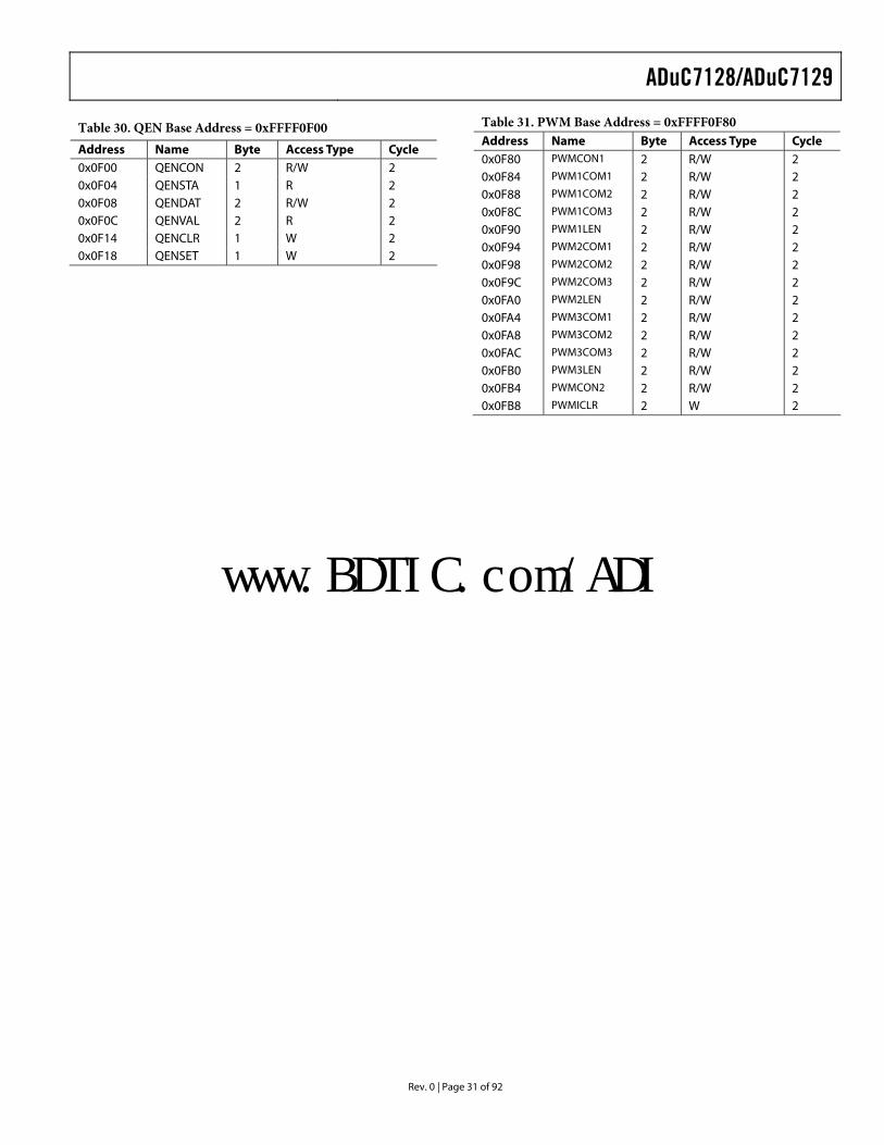
Table 30. QEN Base Address = 0xFFFF0F00
Address Name Byte Access Type Cycle 0x0F00 QENCON 2 R/W 2 0x0F04 QENSTA 1 R 2 0x0F08 QENDAT 2 R/W 2 0x0F0C QENVAL 2 R 2 0x0F14 QENCLR 1 W 2 0x0F18 QENSET 1 W 2
Table 31. PWM Base Address = 0xFFFF0F80 Address Name Byte Access Type Cycle 0x0F80 PWMCON1 2 R/W 2 0x0F84 PWM1COM1 2 R/W 2 0x0F88 PWM1COM2 2 R/W 2 0x0F8C PWM1COM3 2 R/W 2 0x0F90 PWM1LEN 2 R/W 2 0x0F94 PWM2COM1 2 R/W 2 0x0F98 PWM2COM2 2 R/W 2 0x0F9C PWM2COM3 2 R/W 2 0x0FA0 PWM2LEN 2 R/W 2 0x0FA4 PWM3COM1 2 R/W 2 0x0FA8 PWM3COM2 2 R/W 2 0x0FAC PWM3COM3 2 R/W 2 0x0FB0 PWM3LEN 2 R/W 2 0x0FB4 PWMCON2 2 R/W 2 0x0FB8 PWMICLR 2 W 2
www.BDTIC.com/ADI
ADuC7128/ADuC7129
Rev. 0 | Page 32 of 92
ADC CIRCUIT OVERVIEWThe analog-to-digital converter (ADC) incorporates a fast, multichannel, 12-bit ADC. It can operate from 3.0 V to 3.6 V supplies and is capable of providing a throughput of up to 1 MSPS when the clock source is 41.78 MHz. This block provides the user with a multichannel multiplexer, differential track-and-hold, on-chip reference, and ADC.
The ADC consists of a 12-bit successive approximation converter based around two capacitor DACs. Depending on the input signal configuration, the ADC can operate in one of the following three modes:
• Fully differential mode, for small and balanced signals • Single-ended mode, for any single-ended signals • Pseudo differential mode, for any single-ended signals,
taking advantage of the common mode rejection offered by the pseudo differential input
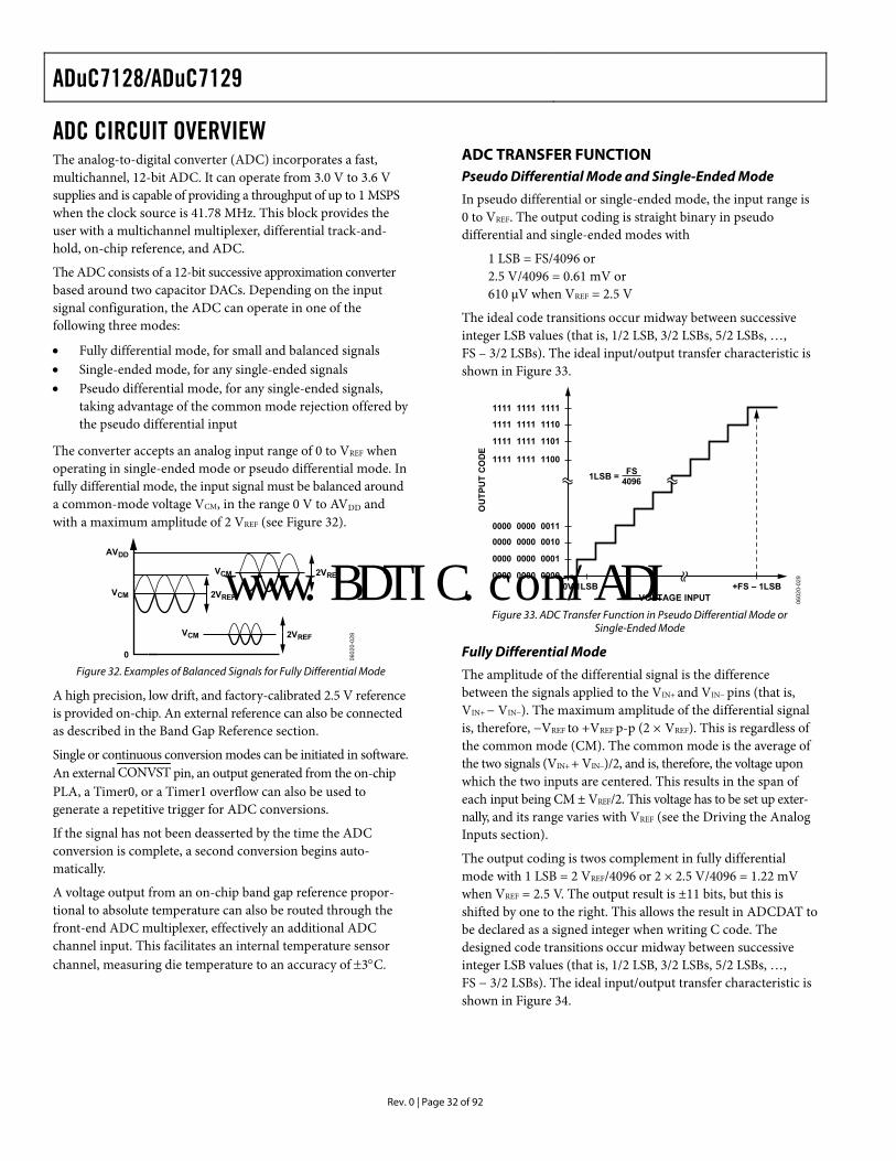
The converter accepts an analog input range of 0 to VREF when operating in single-ended mode or pseudo differential mode. In fully differential mode, the input signal must be balanced around a common-mode voltage VCM, in the range 0 V to AVDD and with a maximum amplitude of 2 VREF (see Figure 32).
AVDD
VCM
VCM
VCM
0
2VREF
2VREF
2VREF
0602
0-02
8
Figure 32. Examples of Balanced Signals for Fully Differential Mode
A high precision, low drift, and factory-calibrated 2.5 V reference is provided on-chip. An external reference can also be connected as described in the Band Gap Reference section.
Single or continuous conversion modes can be initiated in software. An external CONVST pin, an output generated from the on-chip PLA, a Timer0, or a Timer1 overflow can also be used to generate a repetitive trigger for ADC conversions.
If the signal has not been deasserted by the time the ADC conversion is complete, a second conversion begins auto-matically.
A voltage output from an on-chip band gap reference propor-tional to absolute temperature can also be routed through the front-end ADC multiplexer, effectively an additional ADC channel input. This facilitates an internal temperature sensor channel, measuring die temperature to an accuracy of ±3°C.
ADC TRANSFER FUNCTION Pseudo Differential Mode and Single-Ended Mode
In pseudo differential or single-ended mode, the input range is 0 to VREF. The output coding is straight binary in pseudo differential and single-ended modes with
1 LSB = FS/4096 or 2.5 V/4096 = 0.61 mV or 610 μV when VREF = 2.5 V
The ideal code transitions occur midway between successive integer LSB values (that is, 1/2 LSB, 3/2 LSBs, 5/2 LSBs, …, FS – 3/2 LSBs). The ideal input/output transfer characteristic is shown in Figure 33.
OU
TPU
T C
OD
E
VOLTAGE INPUT
1111 1111 1111
1111 1111 1110
1111 1111 1101
1111 1111 1100
0000 0000 0011
1LSB0V +FS – 1LSB
0000 0000 0010
0000 0000 0001
0000 0000 0000
1LSB = FS4096
0602
0-02
9
Figure 33. ADC Transfer Function in Pseudo Differential Mode or
Single-Ended Mode
Fully Differential Mode
The amplitude of the differential signal is the difference between the signals applied to the VIN+ and VIN− pins (that is, VIN+ − VIN−). The maximum amplitude of the differential signal is, therefore, −VREF to +VREF p-p (2 × VREF). This is regardless of the common mode (CM). The common mode is the average of the two signals (VIN+ + VIN−)/2, and is, therefore, the voltage upon which the two inputs are centered. This results in the span of each input being CM ± VREF/2. This voltage has to be set up exter-nally, and its range varies with VREF (see the Driving the Analog Inputs section).
The output coding is twos complement in fully differential mode with 1 LSB = 2 VREF/4096 or 2 × 2.5 V/4096 = 1.22 mV when VREF = 2.5 V. The output result is ±11 bits, but this is shifted by one to the right. This allows the result in ADCDAT to be declared as a signed integer when writing C code. The designed code transitions occur midway between successive integer LSB values (that is, 1/2 LSB, 3/2 LSBs, 5/2 LSBs, …, FS − 3/2 LSBs). The ideal input/output transfer characteristic is shown in Figure 34.
www.BDTIC.com/ADI
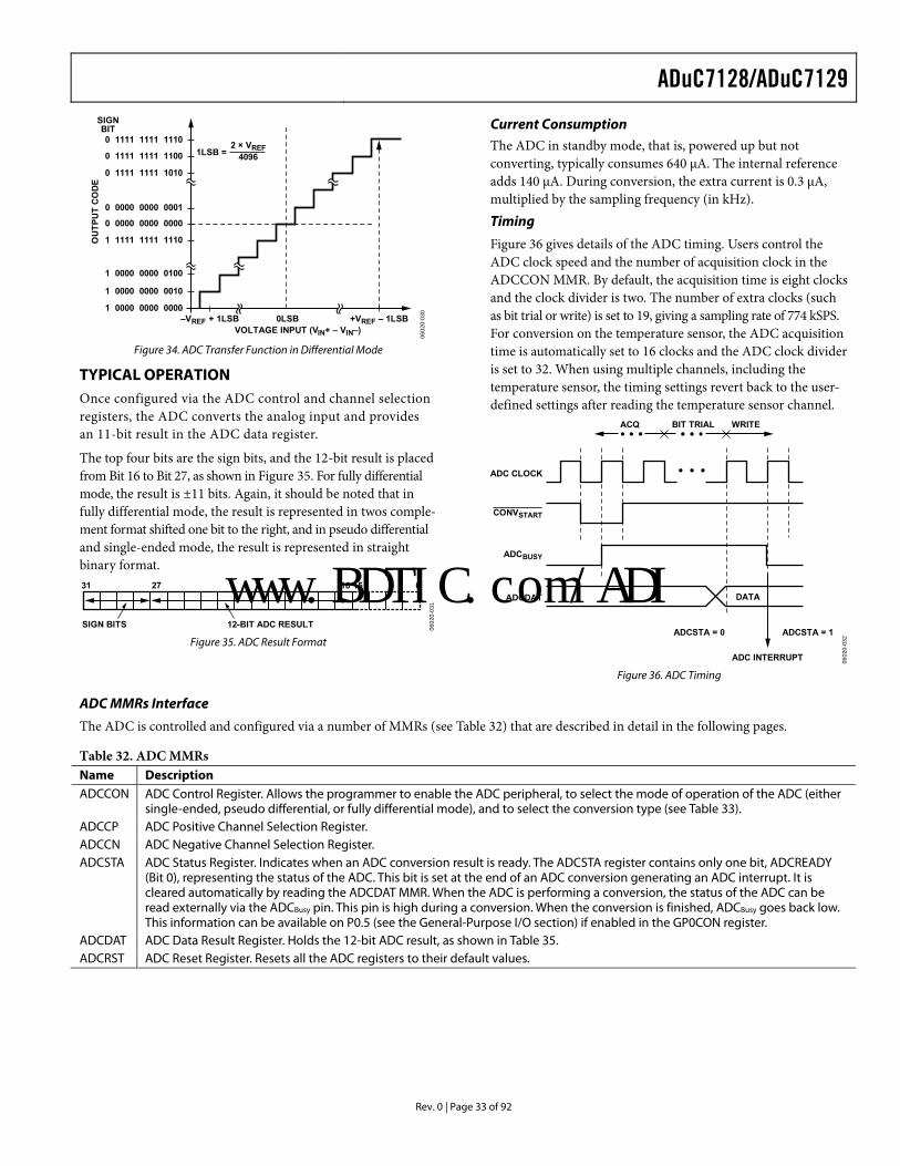
ADuC7128/ADuC7129
Rev. 0 | Page 33 of 92
OU
TPU
T C
OD
E
VOLTAGE INPUT (VIN+ – VIN–)
0 1111 1111 1110
0 1111 1111 1100
0 1111 1111 1010
0 0000 0000 0001
0 0000 0000 0000
1 1111 1111 1110
1 0000 0000 0100
1 0000 0000 0010
1 0000 0000 0000–VREF + 1LSB +VREF – 1LSB0LSB
1LSB =2 × VREF
4096
SIGNBIT
0602
0-03
0
Current Consumption
The ADC in standby mode, that is, powered up but not converting, typically consumes 640 μA. The internal reference adds 140 μA. During conversion, the extra current is 0.3 μA, multiplied by the sampling frequency (in kHz).
Timing
Figure 36 gives details of the ADC timing. Users control the ADC clock speed and the number of acquisition clock in the ADCCON MMR. By default, the acquisition time is eight clocks and the clock divider is two. The number of extra clocks (such as bit trial or write) is set to 19, giving a sampling rate of 774 kSPS. For conversion on the temperature sensor, the ADC acquisition time is automatically set to 16 clocks and the ADC clock divider is set to 32. When using multiple channels, including the temperature sensor, the timing settings revert back to the user-defined settings after reading the temperature sensor channel.
Figure 34. ADC Transfer Function in Differential Mode
TYPICAL OPERATION Once configured via the ADC control and channel selection registers, the ADC converts the analog input and provides an 11-bit result in the ADC data register.
ADC CLOCK
ACQ BIT TRIAL
DATA
ADCSTA = 0 ADCSTA = 1
ADC INTERRUPT
WRITE
CONVSTART
ADCBUSY
ADCDAT
0602
0-03
2
The top four bits are the sign bits, and the 12-bit result is placed from Bit 16 to Bit 27, as shown in Figure 35. For fully differential mode, the result is ±11 bits. Again, it should be noted that in fully differential mode, the result is represented in twos comple-ment format shifted one bit to the right, and in pseudo differential and single-ended mode, the result is represented in straight binary format.
SIGN BITS 12-BIT ADC RESULT
31 27 16 15 0
0602
0-03
1
Figure 35. ADC Result Format
Figure 36. ADC Timing
ADC MMRs Interface
The ADC is controlled and configured via a number of MMRs (see Table 32) that are described in detail in the following pages.
Table 32. ADC MMRs Name Description ADCCON ADC Control Register. Allows the programmer to enable the ADC peripheral, to select the mode of operation of the ADC (either
single-ended, pseudo differential, or fully differential mode), and to select the conversion type (see Table 33). ADCCP ADC Positive Channel Selection Register. ADCCN ADC Negative Channel Selection Register. ADCSTA ADC Status Register. Indicates when an ADC conversion result is ready. The ADCSTA register contains only one bit, ADCREADY
(Bit 0), representing the status of the ADC. This bit is set at the end of an ADC conversion generating an ADC interrupt. It is cleared automatically by reading the ADCDAT MMR. When the ADC is performing a conversion, the status of the ADC can be read externally via the ADCBusy pin. This pin is high during a conversion. When the conversion is finished, ADCBusy goes back low. This information can be available on P0.5 (see the General-Purpose I/O section) if enabled in the GP0CON register.
ADCDAT ADC Data Result Register. Holds the 12-bit ADC result, as shown in Table 35. ADCRST ADC Reset Register. Resets all the ADC registers to their default values.
www.BDTIC.com/ADI
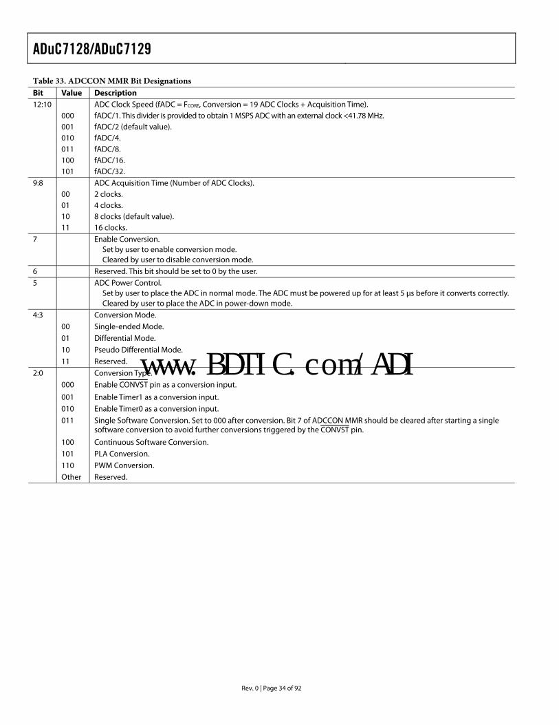
ADuC7128/ADuC7129
Rev. 0 | Page 34 of 92
Table 33. ADCCON MMR Bit Designations Bit Value Description 12:10 ADC Clock Speed (fADC = FCORE, Conversion = 19 ADC Clocks + Acquisition Time). 000 fADC/1. This divider is provided to obtain 1 MSPS ADC with an external clock <41.78 MHz. 001 fADC/2 (default value). 010 fADC/4. 011 fADC/8. 100 fADC/16. 101 fADC/32. 9:8 ADC Acquisition Time (Number of ADC Clocks). 00 2 clocks. 01 4 clocks. 10 8 clocks (default value). 11 16 clocks. 7 Enable Conversion.
Set by user to enable conversion mode. Cleared by user to disable conversion mode.
6 Reserved. This bit should be set to 0 by the user. 5 ADC Power Control.
Set by user to place the ADC in normal mode. The ADC must be powered up for at least 5 μs before it converts correctly. Cleared by user to place the ADC in power-down mode.
Conversion Mode. 00 Single-ended Mode. 01 Differential Mode. 10 Pseudo Differential Mode.
4:3
11 Reserved. Conversion Type. 000 Enable CONVST pin as a conversion input.
001 Enable Timer1 as a conversion input. 010 Enable Timer0 as a conversion input. 011 Single Software Conversion. Set to 000 after conversion. Bit 7 of ADCCON MMR should be cleared after starting a single
software conversion to avoid further conversions triggered by the CONVST pin.
100 Continuous Software Conversion. 101 PLA Conversion. 110 PWM Conversion.
2:0
Other Reserved.
www.BDTIC.com/ADI
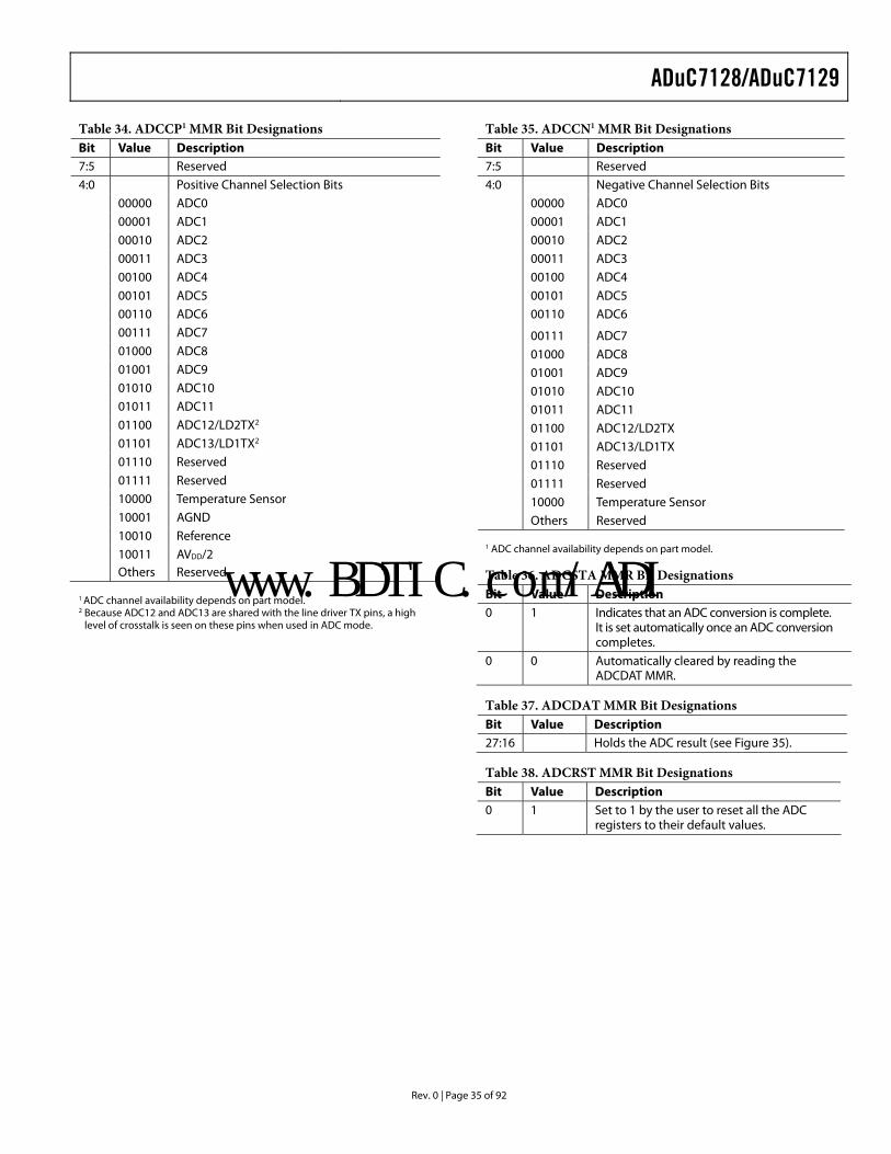
ADuC7128/ADuC7129
Rev. 0 | Page 35 of 92
Table 34. ADCCP1 MMR Bit Designations Bit Value Description 7:5 Reserved
Positive Channel Selection Bits 00000 ADC0 00001 ADC1 00010 ADC2 00011 ADC3 00100 ADC4 00101 ADC5 00110 ADC6 00111 ADC7 01000 ADC8 01001 ADC9 01010 ADC10 01011 ADC11 01100 ADC12/LD2TX2 01101 ADC13/LD1TX2 01110 Reserved 01111 Reserved 10000 Temperature Sensor 10001 AGND 10010 Reference
4:0
10011 AVDD/2 Others Reserved 1 ADC channel availability depends on part model. 2 Because ADC12 and ADC13 are shared with the line driver TX pins, a high
level of crosstalk is seen on these pins when used in ADC mode.
Table 35. ADCCN1 MMR Bit Designations Bit Value Description 7:5 Reserved
Negative Channel Selection Bits 00000 ADC0 00001 ADC1 00010 ADC2 00011 ADC3 00100 ADC4 00101 ADC5 00110 ADC6
00111 ADC7 01000 ADC8 01001 ADC9 01010 ADC10 01011 ADC11 01100 ADC12/LD2TX 01101 ADC13/LD1TX 01110 Reserved 01111 Reserved 10000 Temperature Sensor
4:0
Others Reserved 1 ADC channel availability depends on part model.
Table 36. ADCSTA MMR Bit Designations Bit Value Description 0 1 Indicates that an ADC conversion is complete.
It is set automatically once an ADC conversion completes.
0 0 Automatically cleared by reading the ADCDAT MMR.
Table 37. ADCDAT MMR Bit Designations Bit Value Description 27:16 Holds the ADC result (see Figure 35).
Table 38. ADCRST MMR Bit Designations Bit Value Description 0 1 Set to 1 by the user to reset all the ADC
registers to their default values.
www.BDTIC.com/ADI
ADuC7128/ADuC7129
Rev. 0 | Page 36 of 92
CONVERTER OPERATION The ADC incorporates a successive approximation (SAR) architecture involving a charge-sampled input stage. This architecture is described for the three different modes of operation: differential mode, pseudo differential mode, and single-ended mode.
Differential Mode
The ADuC7128/ADuC7129 contain a successive approximation ADC based on two capacitive DACs. Figure 37 and Figure 38 show simplified schematics of the ADC in acquisition and conversion phase, respectively. The ADC comprises control logic, a SAR, and two capacitive DACs. In Figure 37 (the acquisition phase), SW3 is closed and SW1 and SW2 are in Position A. The comparator is held in a balanced condition, and the sampling capacitor arrays acquire the differential signal on the input.
CAPACITIVEDAC
CAPACITIVEDAC
CONTROLLOGIC
COMPARATOR
SW3SW1
A
A
B
B
SW2
CS
CS
VREF
AIN0
AIN13
MUX
CHANNEL+
CHANNEL–
0602
0-03
3
Figure 37. ADC Acquisition Phase
When the ADC starts a conversion (see Figure 38), SW3 opens and SW1 and SW2 move to Position B, causing the comparator to become unbalanced. Both inputs are disconnected once the conversion begins. The control logic and the charge redistribution DACs are used to add and subtract fixed amounts of charge from the sampling capacitor arrays to bring the comparator back into a balanced condition. When the comparator is rebalanced, the conversion is complete. The control logic generates the ADC output code. The output impedances of the sources driving the VIN+ pin and the VIN− pin must be matched; otherwise, the two inputs have different settling times, resulting in errors.
CAPACITIVEDAC
CAPACITIVEDAC
CONTROLLOGIC
COMPARATOR
SW3SW1
A
A
B
B
SW2
CS
CS
VREF
AIN0
AIN13
MUX
CHANNEL+
CHANNEL–
0602
0-03
4
Figure 38. ADC Conversion Phase
Pseudo Differential Mode
In pseudo differential mode, Channel− is linked to the VIN− pin of the ADuC7128/ADuC7129, and SW2 switches between A (Channel−) and B (VREF). The VIN− pin must be connected to ground or a low voltage. The input signal on VIN+ can then vary from VIN− to VREF + VIN−. Note that VIN− must be chosen so that VREF + VIN− does not exceed AVDD.
CAPACITIVEDAC
CAPACITIVEDAC
CONTROLLOGIC
COMPARATOR
SW3SW1
A
A
B
B
SW2
CS
CS
VREF
AIN0
AIN13
VIN–
MUX
CHANNEL+
CHANNEL–
0602
0-03
5
Figure 39. ADC in Pseudo Differential Mode
Single-Ended Mode
In single-ended mode, SW2 is always connected internally to ground. The VIN− pin can be floating. The input signal range on VIN+ is 0 V to VREF.
CAPACITIVEDAC
CAPACITIVEDAC
CONTROLLOGIC
COMPARATOR
SW3SW1A
B CS
CS
AIN0
AIN13
MUX
CHANNEL+
CHANNEL–
0602
0-03
6
Figure 40. ADC in Single-Ended Mode
Analog Input Structure
Figure 41 shows the equivalent circuit of the analog input structure of the ADC. The four diodes provide ESD protection for the analog inputs. Care must be taken to ensure that the analog input signals never exceed the supply rails by more than 300 mV. Voltage in excess of 300 mV would cause these diodes to become forward biased and start conducting into the substrate. These diodes can conduct up to 10 mA without causing irreversible damage to the part.
The C1 capacitors in Figure 41 are typically 4 pF and can be primarily attributed to pin capacitance. The resistors are lumped components made up of the on resistance of the switches. The value of these resistors is typically about 100 Ω. The C2 capacitors are the ADC sampling capacitors and have a capacitance of 16 pF typical.
www.BDTIC.com/ADI
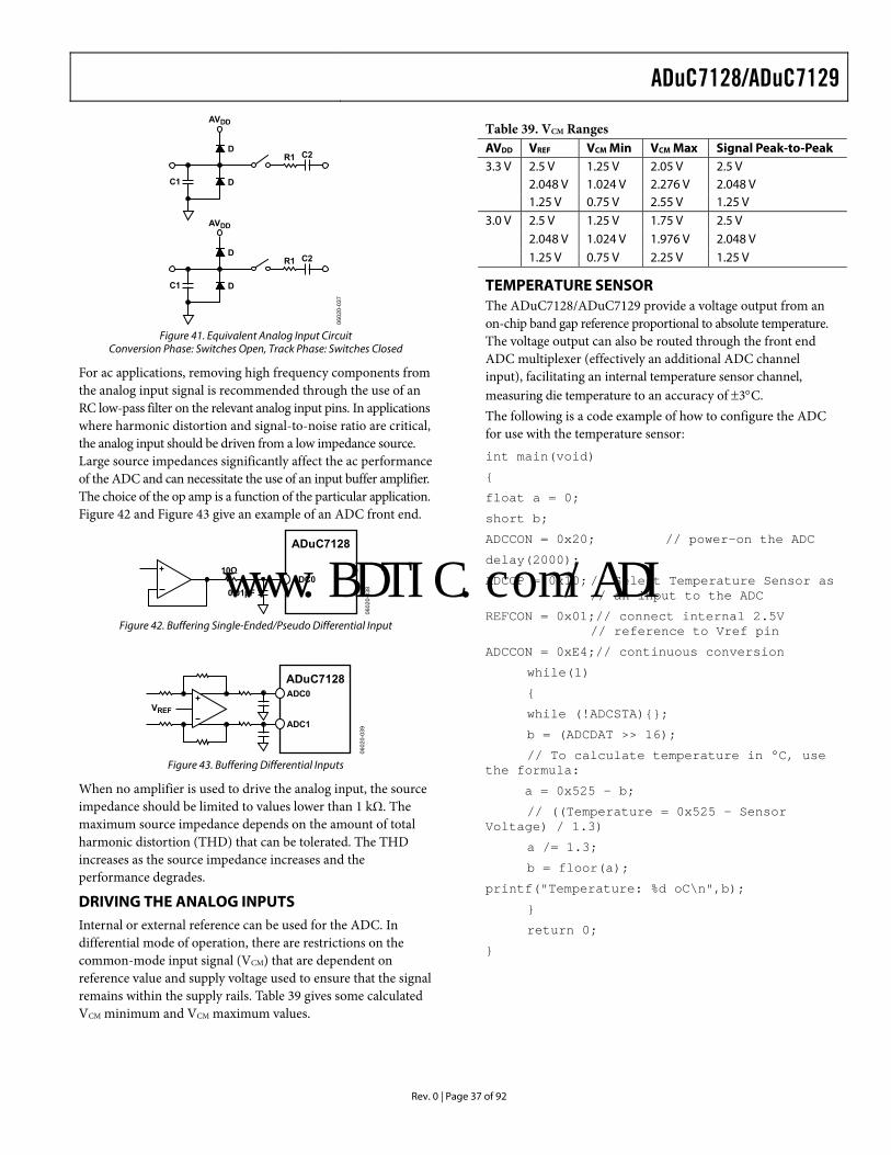
ADuC7128/ADuC7129
Rev. 0 | Page 37 of 92
AVDD
C1
D
D
R1 C2
AVDD
C1
D
D
R1 C2
0602
0-03
7
Figure 41. Equivalent Analog Input Circuit
Conversion Phase: Switches Open, Track Phase: Switches Closed
For ac applications, removing high frequency components from the analog input signal is recommended through the use of an RC low-pass filter on the relevant analog input pins. In applications where harmonic distortion and signal-to-noise ratio are critical, the analog input should be driven from a low impedance source. Large source impedances significantly affect the ac performance of the ADC and can necessitate the use of an input buffer amplifier. The choice of the op amp is a function of the particular application. Figure 42 and Figure 43 give an example of an ADC front end.
ADuC7128
ADC010Ω
0.01µF
0602
0-03
8
Figure 42. Buffering Single-Ended/Pseudo Differential Input
ADuC7128ADC0
VREF
ADC1
0602
0-03
9
Figure 43. Buffering Differential Inputs
When no amplifier is used to drive the analog input, the source impedance should be limited to values lower than 1 kΩ. The maximum source impedance depends on the amount of total harmonic distortion (THD) that can be tolerated. The THD increases as the source impedance increases and the performance degrades.
DRIVING THE ANALOG INPUTS Internal or external reference can be used for the ADC. In differential mode of operation, there are restrictions on the common-mode input signal (VCM) that are dependent on reference value and supply voltage used to ensure that the signal remains within the supply rails. gives some calculated V
Table 39CM minimum and VCM maximum values.
Table 39. VCM Ranges AVDD VREF VCM Min VCM Max Signal Peak-to-Peak
2.5 V 1.25 V 2.05 V 2.5 V 2.048 V 1.024 V 2.276 V 2.048 V
3.3 V
1.25 V 0.75 V 2.55 V 1.25 V 2.5 V 1.25 V 1.75 V 2.5 V 2.048 V 1.024 V 1.976 V 2.048 V
3.0 V
1.25 V 0.75 V 2.25 V 1.25 V
TEMPERATURE SENSOR The ADuC7128/ADuC7129 provide a voltage output from an on-chip band gap reference proportional to absolute temperature. The voltage output can also be routed through the front end ADC multiplexer (effectively an additional ADC channel input), facilitating an internal temperature sensor channel, measuring die temperature to an accuracy of ±3°C. The following is a code example of how to configure the ADC for use with the temperature sensor: int main(void)
float a = 0;
short b;
ADCCON = 0x20; // power-on the ADC
delay(2000);
ADCCP = 0x10; // Select Temperature Sensor as // an input to the ADC
REFCON = 0x01;// connect internal 2.5V // reference to Vref pin
ADCCON = 0xE4;// continuous conversion
while(1)
while (!ADCSTA);
b = (ADCDAT >> 16);
// To calculate temperature in °C, use the formula:
a = 0x525 - b;
// ((Temperature = 0x525 - Sensor Voltage) / 1.3)
a /= 1.3;
b = floor(a);
printf("Temperature: %d oC\n",b);
return 0;
www.BDTIC.com/ADI
ADuC7128/ADuC7129
Rev. 0 | Page 38 of 92
BAND GAP REFERENCE The ADuC7128/ADuC7129 provide an on-chip band gap reference of 2.5 V that can be used for the ADC and for the DAC. This internal reference also appears on the VREF pin. When using the internal reference, a capacitor of 0.47 μF must be connected from the external VREF pin to AGND to ensure stability and fast response during ADC conversions. This reference can also be connected to an external pin (VREF) and used as a reference for other circuits in the system.
An external buffer is required because of the low drive capability of the VREF output. A programmable option also allows an external reference input on the VREF pin. Note that it is not possible to disable the internal reference. Therefore, the external reference source must be capable of overdriving the internal reference source.
The band gap reference interface consists of an 8-bit REFCON MMR, described in Table 40.
Table 40. REFCON MMR Bit Designations Bit Description 7:1 Reserved. 0 Internal Reference Output Enable. Set by user to connect the internal 2.5 V reference to the VREF pin. The reference can be used for external components but needs
to be buffered. Cleared by user to disconnect the reference from the VREF pin. Note: The on-chip DAC is functional only with the internal reference output enable bit set. It does not work with an external
reference.
www.BDTIC.com/ADI
ADuC7128/ADuC7129
Rev. 0 | Page 39 of 92
NONVOLATILE FLASH/EE MEMORYFLASH/EE MEMORY OVERVIEW The ADuC7128/ADuC7129 incorporate Flash/EE memory technology on-chip to provide the user with nonvolatile, in-circuit reprogrammable memory space.
Like EEPROM, Flash memory can be programmed in-system at a byte level, although it must first be erased. The erase is performed in page blocks. As a result, Flash memory is often, and more correctly, referred to as Flash/EE memory.
Overall, Flash/EE memory represents a step closer to the ideal memory device that includes nonvolatility, in-circuit programmability, high density, and low cost. Incorporated in the ADuC7128/ADuC7129, Flash/EE memory technology allows the user to update program code space in-circuit, without the need to replace one-time programmable (OTP) devices at remote operating nodes.
FLASH/EE MEMORY The ADuC7128/ADuC7129 contain two 64 kB arrays of Flash/EE memory. In the first block, the lower 62 kB are available to the user and the upper 2 kB of this Flash/EE program memory array contain permanently embedded firmware, allowing in-circuit serial download. The 2 kB of embedded firmware also contain a power-on configuration routine that downloads factory calibrated coefficients to the various calibrated peripherals, such as band gap references. This 2 kB embedded firmware is hidden from user code. It is not possible for the user to read, write, or erase this page. In the second block, all 64 kB of Flash/EE memory are available to the user.
The 126 kB of Flash/EE memory can be programmed in-circuit, using the serial download mode or the JTAG mode provided.
Flash/EE Memory Reliability
The Flash/EE memory arrays on the parts are fully qualified for two key Flash/EE memory characteristics: Flash/EE memory cycling endurance and Flash/EE memory data retention.
Endurance quantifies the ability of the Flash/EE memory to be cycled through many program, read, and erase cycles. A single endurance cycle is composed of four independent, sequential events, defined as
1. Initial page erase sequence 2. Read/verify, sequence a single Flash/EE location 3. Byte program sequence memory 4. Second read/verify sequence endurance cycle
In reliability qualification, every half word (16-bit wide) location of the three pages (top, middle, and bottom) in the Flash/EE memory is cycled 10,000 times from 0x0000 to 0xFFFF.
As indicated in Table 1 of the Specifications section, the Flash/EE memory endurance qualification is carried out in accordance with JEDEC Retention Lifetime Specification A117 over the industrial temperature range of –40° to +125°C. The results allow the specification of a minimum endurance figure over a supply temperature of 10,000 cycles.
Retention quantifies the ability of the Flash/EE memory to retain its programmed data over time. Again, the parts are qualified in accordance with the formal JEDEC Retention Lifetime Specification (A117) at a specific junction temperature (TJ = 85°C). As part of this qualification procedure, the Flash/EE memory is cycled to its specified endurance limit, described previously, before data retention is characterized. This means that the Flash/EE memory is guaranteed to retain its data for its fully specified retention lifetime every time the Flash/EE memory is reprogrammed. Note, too, that retention lifetime, based on an activation energy of 0.6 eV, derates with TJ, as shown in Figure 44.
150
300
450
600
30 40 55 70 85 100 125 135 150
RET
ENTI
ON
(Yea
rs)
0 0495
5-08
5
JUNCTION TEMPERATURE (°C)
Figure 44. Flash/EE Memory Data Retention
Serial Downloading (In-Circuit Programming)
The ADuC7128/ADuC7129 facilitate code download via the standard UART serial port. The ADuC7128/ADuC7129 enter serial download mode after a reset or power cycle if the BM pin is pulled low through an external 1 kΩ resistor. Once in serial download mode, the user can download code to the full 126 kB of Flash/EE memory while the device is in-circuit in its target appli-cation hardware. A PC serial download executable is provided as part of the development system for serial downloads via the UART.
For additional information, an application note is available at www.analog.com/microconverter describing the protocol for serial downloads via the UART.
JTAG Access
The JTAG protocol uses the on-chip JTAG interface to facilitate code download and debug.
www.BDTIC.com/ADI
ADuC7128/ADuC7129
Rev. 0 | Page 40 of 92
FLASH/EE MEMORY SECURITY The 126 kB of Flash/EE memory available to the user can be read and write protected. Bit 31 of the FEE0PRO/FEE0HID MMR protects the 126 kB from being read through JTAG and also in parallel programming mode. The other 31 bits of this register protect writing to the Flash/EE memory; each bit protects four pages, that is, 2 kB. Write protection is activated for all access types. FEE1PRO and FEE1HID similarly protect the second 64 kB block. All 32 bits of this are used to protect four pages at a time.
Three Levels of Protection
Protection can be set and removed by writing directly into FEExHID MMR. This protection does not remain after reset.
Protection can be set by writing into FEExPRO MMR. It takes effect only after a save protection command (0x0C) and a reset. The FEExPRO MMR is protected by a key to avoid direct access. The key is saved once and must be entered again to modify FEExPRO. A mass erase sets the key back to 0xFFFF but also erases all the user code.
The Flash/EE memory can be permanently protected by using the FEEPRO MMR and a particular value of the 0xDEADDEAD key. Entering the key again to modify the FEExPRO register is not allowed.
Sequence to Write the Key
1. Write the bit in FEExPRO corresponding to the page to be protected.
2. Enable key protection by setting Bit 6 of FEExMOD (Bit 5 must equal 0).
3. Write a 32-bit key in FEExADR, FEExDAT. 4. Run the write key command 0×0C in FEExCON; wait for
the read to be successful by monitoring FEExSTA. 5. Reset the part.
To remove or modify the protection, the same sequence is used with a modified value of FEExPRO. If the key chosen is the value 0xDEAD, then the memory protection cannot be removed. Only a mass erase unprotects the part, but it also erases all user code.
The sequence to write the key is shown in the following example; this protects writing Page 4 to Page 7 of the Flash/EE memory:
FEE0PRO=0xFFFFFFFD; //Protect pages 4 to 7 FEE0MOD=0x48; //Write key enable FEE0ADR=0x1234; //16 bit key value FEE0DAT=0x5678; //16 bit key value FEE0CON= 0x0C; // Write key command
The same sequence should be followed to protect the part permanently with FEExADR = 0xDEAD and FEExDAT = 0xDEAD.
FLASH/EE CONTROL INTERFACE FEE0DAT Register Name Address Default Value Access FEE0DAT 0xFFFF0E0C 0xXXXX R/W
FEE0DAT is a 16-bit data register.
FEE0ADR Register Name Address Default Value Access FEE0ADR 0xFFFF0E10 0x0000 R/W
FEE0ADR is a 16-bit address register.
FEE0SGN Register Name Address Default Value Access FEE0SGN 0xFFFF0E18 0xFFFFFF R
FEE0SGN is a 24-bit code signature.
FEE0PRO Register Name Address Default Value Access FEE0PRO 0xFFFF0E1C 0x00000000 R/W
FEE0PRO provides protection following subsequent reset MMR. It requires a software key (see Table 44).
FEE0HID Register Name Address Default Value Access FEE0HID 0xFFFF0E20 0xFFFFFFFF R/W
FEE0HID provides immediate protection MMR. It does not require any software keys (see Table 44).
Command Sequence for Executing a Mass Erase
FEE0DAT = 0x3CFF; FEE0ADR = 0xFFC3; FEE0MOD = FEE0MOD|0x8; //Erase key enable FEE0CON = 0x06; //Mass erase command
www.BDTIC.com/ADI
ADuC7128/ADuC7129
Rev. 0 | Page 41 of 92
FEE1DAT Register Name Address Default Value Access FEE1DAT 0xFFFF0E8C 0xXXXX R/W
FEE1DAT is a 16-bit data register.
FEE1ADR Register Name Address Default Value Access FEE1ADR 0xFFFF0E90 0x0000 R/W
FEE1ADR is a 16-bit address register.
FEE1SGN Register Name Address Default Value Access FEE1SGN 0xFFFF0E98 0xFFFFFF R
FEE1SGN is a 24-bit code signature.
FEE1PRO Register Name Address Default Value Access FEE1PRO 0xFFFF0E9C 0x00000000 R/W
FEE1PRO provides protection following subsequent reset MMR. It requires a software key (see Table 45).
FEE1HID Register Name Address Default Value Access FEE1HID 0xFFFF0EA0 0xFFFFFFFF R/W
FEE1HID provides immediate protection MMR. It does not require any software keys (see Table 45).
FEE0STA Register Name Address Default Value Access FEE0STA 0xFFFF0E00 0x0000 R/W
FEE1STA Register Name Address Default Value Access FEE1STA 0xFFFF0E80 0x0000 R/W
FEE0MOD Register Name Address Default Value Access FEE0MOD 0xFFFF0E04 0x80 R/W
FEE1MOD Register Name Address Default Value Access FEE1MOD 0xFFFF0E84 0x80 R/W
FEE0CON Register Name Address Default Value Access FEE0CON 0xFFFF0E08 0x0000 R/W
FEE1CON Register Name Address Default Value Access FEE1CON 0xFFFF0E88 0x0000 R/W
www.BDTIC.com/ADI
ADuC7128/ADuC7129
Rev. 0 | Page 42 of 92
Table 41. FEExSTA MMR Bit Designations Bit Description 15:6 Reserved. 5 Reserved. 4 Reserved. 3 Flash/EE Interrupt Status Bit.
Set automatically when an interrupt occurs, that is, when a command is complete and the Flash/EE interrupt enable bit in the FEExMOD register is set. Cleared when reading FEExSTA register.
2 Flash/EE Controller Busy. Set automatically when the controller is busy. Cleared automatically when the controller is not busy.
1 Command Fail. Set automatically when a command completes unsuccessfully. Cleared automatically when reading FEExSTA register.
0 Command Complete. Set by MicroConverter when a command is complete. Cleared automatically when reading FEExSTA register.
Table 42. FEExMOD MMR Bit Designations Bit Description 7:5 Reserved. 4 Flash/EE Interrupt Enable.
Set by user to enable the Flash/EE interrupt. The interrupt occurs when a command is complete. Cleared by user to disable the Flash/EE interrupt
3 Erase/Write Command Protection. Set by user to enable the erase and write commands. Cleared to protect the Flash/EE memory against erase/write command.
2 Reserved. Should always be set to 0 by the user. 1:0 Flash/EE Wait States. Both Flash/EE blocks must have the same wait state value for any change to take effect.
Table 43. Command Codes in FEExCON Code Command Description 0x001 Null Idle State. 0x011 Single read Load FEExDAT with the 16-bit data indexed by FEExADR. 0x021 Single write Write FEExDAT at the address pointed by FEExADR. This operation takes 50 μs. 0x031 Erase/Write Erase the page indexed by FEExADR and write FEExDAT at the location pointed by FEExADR. This operation
takes 20 ms. 0x041 Single verify Compare the contents of the location pointed by FEExADR to the data in FEExDAT. The result of the comparison
is returned in FEExSTA Bit 1. 0x051 Single erase Erase the page indexed by FEExADR. 0x061 Mass erase Erase user space. The 2 kB of kernel are protected in Block 0. This operation takes 2.48 sec. To prevent accidental
execution, a command sequence is required to execute this instruction. 0x07 Reserved Reserved. 0x08 Reserved Reserved. 0x09 Reserved Reserved. 0x0A Reserved Reserved. 0x0B Signature Gives a signature of the 64 kB of Flash/EE in the 24-bit FEExSIGN MMR. This operation takes 32,778 clock cycles. 0x0C Protect This command can be run only once. The value of FEExPRO is saved and can be removed only with a mass erase
(0x06) or with the key. 0x0D Reserved Reserved. 0x0E Reserved Reserved. 0x0F Ping No Operation, Interrupt Generated. 1 The FEExCON register always reads 0x07 immediately after execution of any of these commands.
www.BDTIC.com/ADI
ADuC7128/ADuC7129
Rev. 0 | Page 43 of 92
Table 44. FEE0PRO and FEE0HID MMR Bit Designations Bit Description 31 Read Protection.
Cleared by user to protect Block 0. Set by user to allow reading Block 0.
30:0 Write Protection for Page 123 to Page 120, for Page 119 to Page 116, and for Page 3 to Page 0. Cleared by user to protect the pages in writing. Set by user to allow writing the pages.
Table 45. FEE1PRO and FEE1HID MMR Bit Designations Bit Description 31 Read Protection.
Cleared by user to protect Block 1. Set by user to allow reading Block 1.
30 Write Protection for Page 127 to Page 120. Cleared by user to protect the pages in writing. Set by user to allow writing the pages.
31:0 Write Protection for Page 119 to Page 116 and for Page 3 to Page 0. Cleared by user to protect the pages in writing. Set by user to allow writing the pages.
EXECUTION TIME FROM SRAM AND FLASH/EE This section describes SRAM and Flash/EE access times during execution for applications where execution time is critical.
Execution from SRAM
Fetching instructions from SRAM takes one clock cycle because the access time of the SRAM is 2 ns and a clock cycle is 22 ns minimum. However, if the instruction involves reading or writing data to memory, one extra cycle must be added if the data is in SRAM (or three cycles if the data is in Flash/EE), one cycle to execute the instruction and two cycles to get the 32-bit data from Flash/EE. A control flow instruction, such as a branch instruction, takes one cycle to fetch, but it also takes two cycles to fill the pipeline with the new instructions.
Execution from Flash/EE
Because the Flash/EE width is 16 bits and access time for 16-bit words is 23 ns, execution from Flash/EE cannot be done in one cycle (as can be done from SRAM when the CD bit = 0). In addi-tion, some dead times are needed before accessing data for any value of CD bits.
In ARM mode, where instructions are 32 bits, two cycles are needed to fetch any instruction when CD = 0. In Thumb mode, where instructions are 16 bits, one cycle is needed to fetch any instruction.
Timing is identical in both modes when executing instructions that involve using the Flash/EE for data memory. If the instruction to be executed is a control flow instruction, an extra cycle is needed to decode the new address of the program counter and then four cycles are needed to fill the pipeline. A data processing instruction involving only core registers doesn’t require any extra clock cycles, but if it involves data in Flash/EE, an extra clock cycle is needed to decode the address of the data and two cycles to get the 32-bit data from Flash/EE. An extra cycle must also be added before fetching another instruction. Data transfer instructions are more complex and are summarized in Table 46.
Table 46. Execution Cycles in ARM/Thumb Mode
Instructions Fetch Cycles
Dead Time Data Access
Dead Time
LD 2/1 1 2 1 LDH 2/1 1 1 1 LDM/PUSH 2/1 N 2 × N N STR 2/1 1 2 × 20 μs 1 STRH 2/1 1 20 μs 1 STRM/POP 2/1 N 2 × N × 20 μs N
With 1 < N ≤ 16, N is the number of bytes of data to load or store in the multiple load/store instruction. The SWAP instruction combines an LD and STR instruction with only one fetch, giving a total of eight cycles plus 40 μs.
www.BDTIC.com/ADI
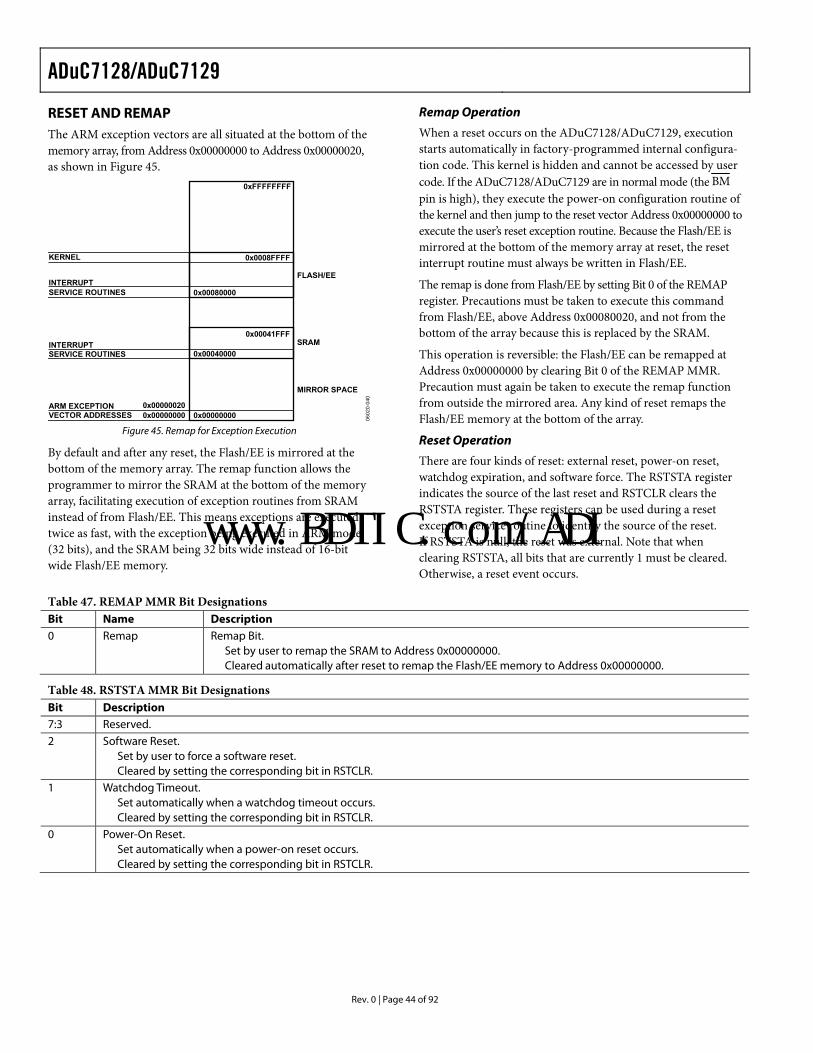
ADuC7128/ADuC7129
Rev. 0 | Page 44 of 92
RESET AND REMAP The ARM exception vectors are all situated at the bottom of the memory array, from Address 0x00000000 to Address 0x00000020, as shown in Figure 45.
KERNEL
INTERRUPTSERVICE ROUTINES
INTERRUPTSERVICE ROUTINES
ARM EXCEPTIONVECTOR ADDRESSES
0x00000020
0x00041FFF
0x0008FFFF
0xFFFFFFFF
FLASH/EE
SRAM
MIRROR SPACE
0x00000000 0x00000000
0x00040000
0x00080000
0602
0-04
0
Figure 45. Remap for Exception Execution
By default and after any reset, the Flash/EE is mirrored at the bottom of the memory array. The remap function allows the programmer to mirror the SRAM at the bottom of the memory array, facilitating execution of exception routines from SRAM instead of from Flash/EE. This means exceptions are executed twice as fast, with the exception being executed in ARM mode (32 bits), and the SRAM being 32 bits wide instead of 16-bit wide Flash/EE memory.
Remap Operation
When a reset occurs on the ADuC7128/ADuC7129, execution starts automatically in factory-programmed internal configura-tion code. This kernel is hidden and cannot be accessed by user code. If the ADuC7128/ADuC7129 are in normal mode (the BM pin is high), they execute the power-on configuration routine of the kernel and then jump to the reset vector Address 0x00000000 to execute the user’s reset exception routine. Because the Flash/EE is mirrored at the bottom of the memory array at reset, the reset interrupt routine must always be written in Flash/EE.
The remap is done from Flash/EE by setting Bit 0 of the REMAP register. Precautions must be taken to execute this command from Flash/EE, above Address 0x00080020, and not from the bottom of the array because this is replaced by the SRAM.
This operation is reversible: the Flash/EE can be remapped at Address 0x00000000 by clearing Bit 0 of the REMAP MMR. Precaution must again be taken to execute the remap function from outside the mirrored area. Any kind of reset remaps the Flash/EE memory at the bottom of the array.
Reset Operation
There are four kinds of reset: external reset, power-on reset, watchdog expiration, and software force. The RSTSTA register indicates the source of the last reset and RSTCLR clears the RSTSTA register. These registers can be used during a reset exception service routine to identify the source of the reset. If RSTSTA is null, the reset was external. Note that when clearing RSTSTA, all bits that are currently 1 must be cleared. Otherwise, a reset event occurs.
Table 47. REMAP MMR Bit Designations Bit Name Description 0 Remap Remap Bit.
Set by user to remap the SRAM to Address 0x00000000. Cleared automatically after reset to remap the Flash/EE memory to Address 0x00000000.
Table 48. RSTSTA MMR Bit Designations Bit Description 7:3 Reserved. 2 Software Reset.
Set by user to force a software reset. Cleared by setting the corresponding bit in RSTCLR.
1 Watchdog Timeout. Set automatically when a watchdog timeout occurs. Cleared by setting the corresponding bit in RSTCLR.
0 Power-On Reset. Set automatically when a power-on reset occurs. Cleared by setting the corresponding bit in RSTCLR.
www.BDTIC.com/ADI
ADuC7128/ADuC7129
Rev. 0 | Page 45 of 92
OTHER ANALOG PERIPHERALSDAC The ADuC7128/ADuC7129 feature a 10-bit current DAC that can be used to generate user-defined waveforms or sine waves generated by the DDS. The DAC consists of a 10-bit IDAC followed by a current-to-voltage conversion.
The current output of the IDAC is passed through a resistor and capacitor network where it is both filtered and converted to a voltage. This voltage is then buffered by an op amp and passed to the line driver.
For the DAC to function, the internal 2.5 V voltage reference must be enabled and driven out onto an external capacitor, REFCON = 0x01.
Once the DAC is enabled, users see a 5 mV drop in the internal reference value. This is due to bias currents drawn from the reference used in the DAC circuitry. It is recommended that if using the DAC, it be left powered on to avoid seeing variations in ADC results.
Table 49. DACCON MMR Bit Designations Bit Value Description
10:9 Reserved. These bits should be written to 0 by the user.
8 Reserved. This bit should be written to 0 by the user.
7 Reserved. This bit should be written to 0 by the user. 6 Reserved. This bit should be written to 0 by the user. 5 Output Enable. This bit operates in all modes. In Line Driver mode, this bit should be set.
Set by user to enable the line driver output. Cleared by user to disable the line driver output. In this mode the line driver output is high impedance.
4 Single-Ended or Differential Output Control. Set by user to operate in differential mode, the output is the differential voltage between LD1TX and LD2TX. The voltage output range is VREF/2 ± VREF/2. Cleared by user to reference the LD1TX output to AGND. The voltage output range is AVDD/2 ± VREF/2.
3 Reserved. This bit should be set to 0 by the user.
Operation Mode Control. This bit selects the mode of operation of the DAC.
00 Power-Down.
01 Reserved.
10 Reserved.
2:1
11 DDS and DAC Mode. Selected by DACEN.
0 DAC Update Rate Control. This bit has no effect when in DDS mode. Set by user to update the DAC on the negative edge of Timer1. This allows the user to use any one of the core CLK, OSC CLK, baud CLK, or user CLK and divide these down by 1, 16, 256, or 32,768. A user can do waveform generation by writing to the DAC data register from RAM and updating the DAC at regular intervals via Timer1. Cleared by user to update the DAC on the negative edge of HCLK.
www.BDTIC.com/ADI
ADuC7128/ADuC7129
Rev. 0 | Page 46 of 92
DACEN Register Name Address Default Value Access DACEN 0xFFFF06B8 0x00 R/W
Table 50. DACEN MMR Bit Designations Bit Description 7:1 Reserved. 0 Set to 1 by the user to enable DAC mode.
Set to 0 by the user to enable DDS mode.
DACDAT Register Name Address Default Value Access DACDAT 0xFFFF06B4 0x0000 R/W
Table 51. DACDAT MMR Bit Designations Bit Description 15:10 Reserved. 9:0 10-bit data for DAC.
The DACDAT MMR controls the output of the DAC. The data written to this register is a ±9-bit signed value. This means that 0x0000 represents midscale, 0x0200 represents zero scale, and 0x01FF represents full scale.
DACEN and DACDAT require key access. To write to these MMRs, use the sequences shown in Table 52.
Table 52. DACEN and DACDAT Write Sequences DACEN DACDAT DACKEY0 = 0x07 DACKEY0 = 0x07 DACEN = user value DACDAT = user value DACKEY1 = 0xB9 DACKEY1 = 0xB9
DDS The DDS is used to generate a digital sine wave signal for the DAC on the ADuC7128/ADuC7129. It can be enabled into a free running mode by the user.
Both the phase and frequency can be controlled.
Table 53. DDSCON MMR Bit Designations Bit Description 7:6 Reserved. 5 DDS Output Enable.
Set by user to enable the DDS output. This has an effect only if the DDS is selected in DACCON. Cleared by user to disable the DDS output.
4 Reserved. Binary Divide Control.
DIV Scale Ratio 0000 0.000 0001 0.125 0010 0.250 0011 0.375 0100 0.500 0101 0.625 0110 0.750 0111 0.875
3:0
1xxx 1.000
www.BDTIC.com/ADI
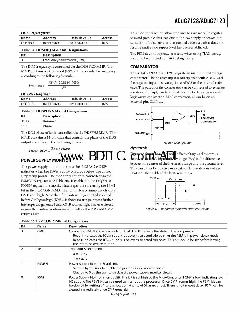
ADuC7128/ADuC7129
Rev. 0 | Page 47 of 92
DDSFRQ Register Name Address Default Value Access DDSFRQ 0xFFFF0694 0x00000000 R/W
Table 54. DDSFRQ MMR Bit Designations Bit Description 31:0 Frequency select word (FSW)
The DDS frequency is controlled via the DDSFRQ MMR. This MMR contains a 32-bit word (FSW) that controls the frequency according to the following formula:
322MHz8896.20×
=FSW
Frequency
DDSPHS Register Name Address Default Value Access DDSPHS 0xFFFF0698 0x00000000 R/W
Table 55. DDSPHS MMR Bit Designations Bit Description 31:12 Reserved 11:0 Phase
The DDS phase offset is controlled via the DDSPHS MMR. This MMR contains a 12-bit value that controls the phase of the DDS output according to the following formula:
1222 PhaseOffsetPhase ×π×
=
POWER SUPPLY MONITOR The power supply monitor on the ADuC7128/ADuC7129 indicates when the IOVDD supply pin drops below one of two supply trip points. The monitor function is controlled via the PSMCON register (see Table 56). If enabled in the IRQEN or FIQEN register, the monitor interrupts the core using the PSMI bit in the PSMCON MMR. This bit is cleared immediately once CMP goes high. Note that if the interrupt generated is exited before CMP goes high (IOVDD is above the trip point), no further interrupts are generated until CMP returns high. The user should ensure that code execution remains within the ISR until CMP returns high.
This monitor function allows the user to save working registers to avoid possible data loss due to the low supply or brown-out conditions. It also ensures that normal code execution does not resume until a safe supply level has been established.
The PSM does not operate correctly when using JTAG debug. It should be disabled in JTAG debug mode.
COMPARATOR The ADuC7128/ADuC7129 integrate an uncommitted voltage comparator. The positive input is multiplexed with ADC2, and the negative input has two options: ADC3 or the internal refer-ence. The output of the comparator can be configured to generate a system interrupt, can be routed directly to the programmable logic array, can start an ADC conversion, or can be on an external pin, CMPOUT.
MUX
CONVERSIONMUX
REF
PLAIRQADC START
ADC2/CMP0
ADC3/CMP1
P0.0/CMPOUT
0602
0-04
2
Figure 46. Comparator
Hysteresis
Figure 47 shows how the input offset voltage and hysteresis terms are defined. Input offset voltage (VOS) is the difference between the center of the hysteresis range and the ground level. This can either be positive or negative. The hysteresis voltage (VH) is ½ the width of the hysteresis range.
COMPOUT
COMP0
VH VH
VOS 0602
0-04
1
Figure 47. Comparator Hysteresis Transfer Function
Table 56. PSMCON MMR Bit Designations Bit Name Description 3 CMP Comparator Bit. This is a read-only bit that directly reflects the state of the comparator.
Read 1 indicates the IOVDD supply is above its selected trip point or the PSM is in power-down mode. Read 0 indicates the IOVDD supply is below its selected trip point. This bit should be set before leaving the interrupt service routine.
Trip Point Selection Bit. 0 = 2.79 V
2 TP
1 = 3.07 V 1 PSMEN Power Supply Monitor Enable Bit.
Set to 1 by the user to enable the power supply monitor circuit. Cleared to 0 by the user to disable the power supply monitor circuit.
0 PSMI Power Supply Monitor Interrupt Bit. This bit is set high by the MicroConverter if CMP is low, indicating low I/O supply. The PSMI bit can be used to interrupt the processor. Once CMP returns high, the PSMI bit can be cleared by writing a 1 to this location. A write of 0 has no effect. There is no timeout delay. PSMI can be cleared immediately once CMP goes high.
www.BDTIC.com/ADI
ADuC7128/ADuC7129
Rev. 0 | Page 48 of 92
Comparator Interface
The comparator interface consists of a 16-bit MMR, CMPCON, described in Table 57.
Table 57. CMPCON MMR Bit Designations Bit Value Name Description 15:11 Reserved. 10 CMPEN Comparator Enable Bit.
Set by user to enable the comparator. Cleared by user to disable the comparator.
Note: A comparator interrupt is generated on the enable of the comparator. This should be cleared in the user software.
Comparator Negative Input Select Bits. 00 AVDD/2. 01 ADC3 input. 10 VREF × 0.6.
9:8
11
CMPIN
Reserved. Comparator Output Configuration Bits. 00 IRQ and PLA connections disabled. 01 IRQ and PLA connections disabled. 10 PLA connections enabled.
7:6
11
CMPOC
IRQ connections enabled. 5 CMPOL Comparator Output Logic State Bit.
When low, the comparator output is high when the positive input (CMP0) is above the negative input (CMP1). When high, the comparator output is high when the positive input is below the negative input.
Response Time. 00 5 μs response time typical for large signals (2.5 V differential).
17 μs response time typical for small signals (0.65 mV differential). 01 Reserved. 10 Reserved.
4:3
11
CMPRES
3 μs response time typical for any signal type. 2 CMPHYST Comparator Hysteresis Bit.
Set by user to have a hysteresis of about 7.5 mV. Cleared by user to have no hysteresis.
1 CMPORI Comparator Output Rising Edge Interrupt. Set automatically when a rising edge occurs on the monitored voltage (CMP0). Cleared by user by writing a 1 to this bit.
0 CMPOFI Comparator Output Falling Edge Interrupt. Set automatically when a falling edge occurs on the monitored voltage (CMP0). Cleared by user.
www.BDTIC.com/ADI
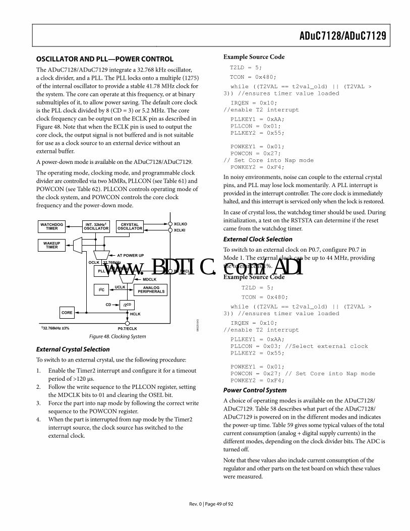
ADuC7128/ADuC7129
Rev. 0 | Page 49 of 92
OSCILLATOR AND PLL—POWER CONTROL The ADuC7128/ADuC7129 integrate a 32.768 kHz oscillator, a clock divider, and a PLL. The PLL locks onto a multiple (1275) of the internal oscillator to provide a stable 41.78 MHz clock for the system. The core can operate at this frequency, or at binary submultiples of it, to allow power saving. The default core clock is the PLL clock divided by 8 (CD = 3) or 5.2 MHz. The core clock frequency can be output on the ECLK pin as described in Figure 48. Note that when the ECLK pin is used to output the core clock, the output signal is not buffered and is not suitable for use as a clock source to an external device without an external buffer.
A power-down mode is available on the ADuC7128/ADuC7129.
The operating mode, clocking mode, and programmable clock divider are controlled via two MMRs, PLLCON (see Table 61) and POWCON (see Table 62). PLLCON controls operating mode of the clock system, and POWCON controls the core clock frequency and the power-down mode.
132.768kHz ±3%
AT POWER UP
40.78MHzOCLK 32.768kHz
WATCHDOGTIMER
INT. 32kHz1OSCILLATOR
CRYSTALOSCILLATOR
WAKEUPTIMER
MDCLK
HCLK
PLL
CORE
I2CUCLK ANALOG
PERIPHERALS
/2CDCD
XCLKOXCLKI
P0.7/XCLK
P0.7/ECLK 0602
0-04
3
Figure 48. Clocking System
External Crystal Selection
To switch to an external crystal, use the following procedure:
1. Enable the Timer2 interrupt and configure it for a timeout period of >120 μs.
2. Follow the write sequence to the PLLCON register, setting the MDCLK bits to 01 and clearing the OSEL bit.
3. Force the part into nap mode by following the correct write sequence to the POWCON register.
4. When the part is interrupted from nap mode by the Timer2 interrupt source, the clock source has switched to the external clock.
Example Source Code T2LD = 5;
TCON = 0x480;
while ((T2VAL == t2val_old) || (T2VAL > 3)) //ensures timer value loaded
IRQEN = 0x10; //enable T2 interrupt
PLLKEY1 = 0xAA; PLLCON = 0x01; PLLKEY2 = 0x55; POWKEY1 = 0x01; POWCON = 0x27; // Set Core into Nap mode POWKEY2 = 0xF4;
In noisy environments, noise can couple to the external crystal pins, and PLL may lose lock momentarily. A PLL interrupt is provided in the interrupt controller. The core clock is immediately halted, and this interrupt is serviced only when the lock is restored.
In case of crystal loss, the watchdog timer should be used. During initialization, a test on the RSTSTA can determine if the reset came from the watchdog timer.
External Clock Selection
To switch to an external clock on P0.7, configure P0.7 in Mode 1. The external clock can be up to 44 MHz, providing the tolerance is 1%.
Example Source Code T2LD = 5;
TCON = 0x480;
while ((T2VAL == t2val_old) || (T2VAL > 3)) //ensures timer value loaded
IRQEN = 0x10; //enable T2 interrupt
PLLKEY1 = 0xAA; PLLCON = 0x03; //Select external clock PLLKEY2 = 0x55; POWKEY1 = 0x01; POWCON = 0x27; // Set Core into Nap mode POWKEY2 = 0xF4;
Power Control System
A choice of operating modes is available on the ADuC7128/ ADuC7129. Table 58 describes what part of the ADuC7128/ ADuC7129 is powered on in the different modes and indicates the power-up time. Table 59 gives some typical values of the total current consumption (analog + digital supply currents) in the different modes, depending on the clock divider bits. The ADC is turned off.
Note that these values also include current consumption of the regulator and other parts on the test board on which these values were measured.
www.BDTIC.com/ADI
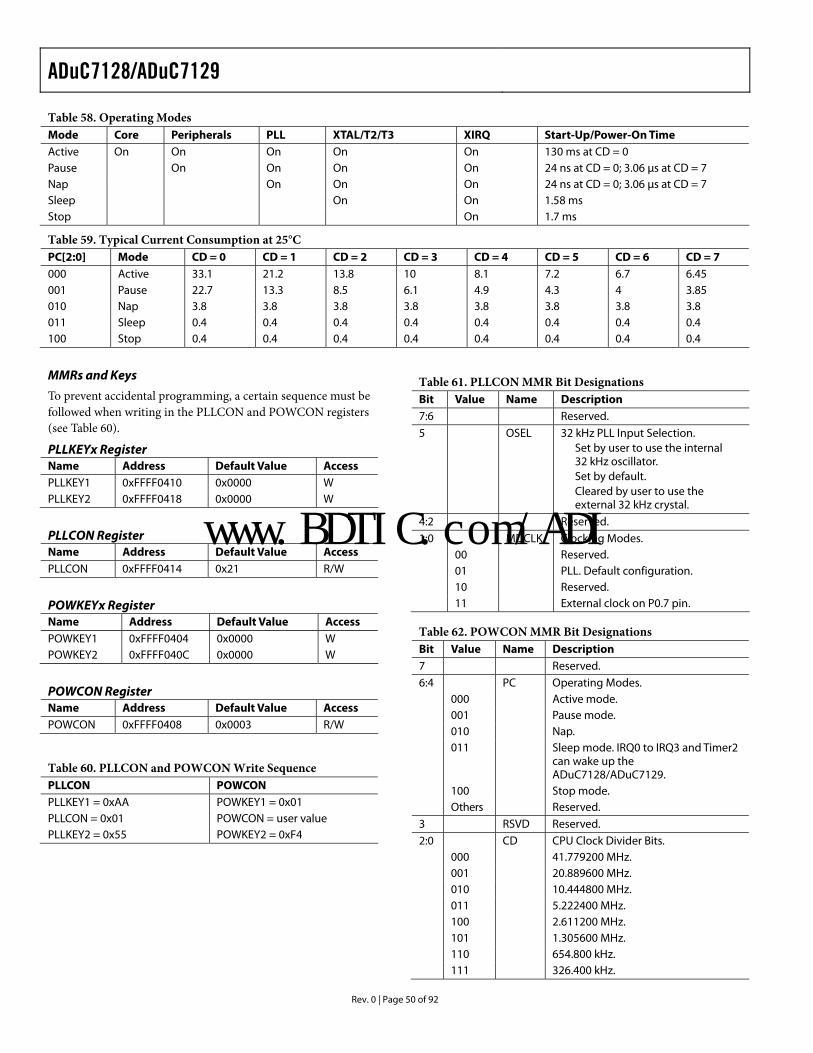
ADuC7128/ADuC7129
Rev. 0 | Page 50 of 92
Table 58. Operating Modes Mode Core Peripherals PLL XTAL/T2/T3 XIRQ Start-Up/Power-On Time Active On On On On On 130 ms at CD = 0 Pause On On On On 24 ns at CD = 0; 3.06 μs at CD = 7 Nap On On On 24 ns at CD = 0; 3.06 μs at CD = 7 Sleep On On 1.58 ms Stop On 1.7 ms
Table 59. Typical Current Consumption at 25°C PC[2:0] Mode CD = 0 CD = 1 CD = 2 CD = 3 CD = 4 CD = 5 CD = 6 CD = 7 000 Active 33.1 21.2 13.8 10 8.1 7.2 6.7 6.45 001 Pause 22.7 13.3 8.5 6.1 4.9 4.3 4 3.85 010 Nap 3.8 3.8 3.8 3.8 3.8 3.8 3.8 3.8 011 Sleep 0.4 0.4 0.4 0.4 0.4 0.4 0.4 0.4 100 Stop 0.4 0.4 0.4 0.4 0.4 0.4 0.4 0.4
MMRs and Keys
To prevent accidental programming, a certain sequence must be followed when writing in the PLLCON and POWCON registers (see Table 60).
PLLKEYx Register Name Address Default Value Access PLLKEY1 0xFFFF0410 0x0000 W PLLKEY2 0xFFFF0418 0x0000 W
PLLCON Register Name Address Default Value Access PLLCON 0xFFFF0414 0x21 R/W
POWKEYx Register Name Address Default Value Access POWKEY1 0xFFFF0404 0x0000 W POWKEY2 0xFFFF040C 0x0000 W
POWCON Register Name Address Default Value Access POWCON 0xFFFF0408 0x0003 R/W
Table 60. PLLCON and POWCON Write Sequence PLLCON POWCON PLLKEY1 = 0xAA POWKEY1 = 0x01 PLLCON = 0x01 POWCON = user value PLLKEY2 = 0x55 POWKEY2 = 0xF4
Table 61. PLLCON MMR Bit Designations Bit Value Name Description 7:6 Reserved. 5 OSEL 32 kHz PLL Input Selection.
Set by user to use the internal 32 kHz oscillator. Set by default. Cleared by user to use the external 32 kHz crystal.
4:2 Reserved. 1:0 MDCLK Clocking Modes. 00 Reserved. 01 PLL. Default configuration. 10 Reserved. 11 External clock on P0.7 pin.
Table 62. POWCON MMR Bit Designations Bit Value Name Description 7 Reserved. 6:4 PC Operating Modes. 000 Active mode. 001 Pause mode. 010 Nap. 011 Sleep mode. IRQ0 to IRQ3 and Timer2
can wake up the ADuC7128/ADuC7129.
100 Stop mode. Others Reserved. 3 RSVD Reserved. 2:0 CD CPU Clock Divider Bits. 000 41.779200 MHz. 001 20.889600 MHz. 010 10.444800 MHz. 011 5.222400 MHz. 100 2.611200 MHz. 101 1.305600 MHz. 110 654.800 kHz. 111 326.400 kHz.
www.BDTIC.com/ADI
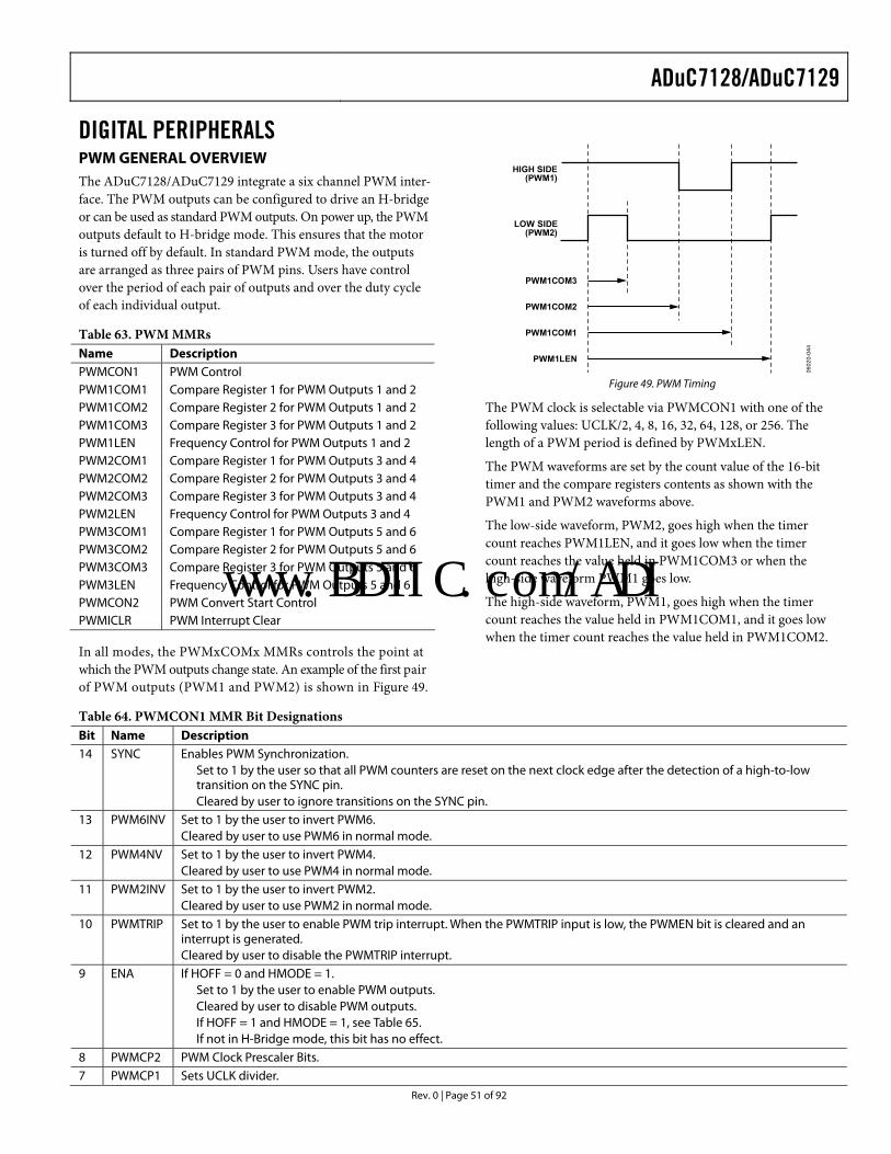
ADuC7128/ADuC7129
Rev. 0 | Page 51 of 92
DIGITAL PERIPHERALSPWM GENERAL OVERVIEW The ADuC7128/ADuC7129 integrate a six channel PWM inter-face. The PWM outputs can be configured to drive an H-bridge or can be used as standard PWM outputs. On power up, the PWM outputs default to H-bridge mode. This ensures that the motor is turned off by default. In standard PWM mode, the outputs are arranged as three pairs of PWM pins. Users have control over the period of each pair of outputs and over the duty cycle of each individual output.
Table 63. PWM MMRs Name Description PWMCON1 PWM Control PWM1COM1 Compare Register 1 for PWM Outputs 1 and 2 PWM1COM2 Compare Register 2 for PWM Outputs 1 and 2 PWM1COM3 Compare Register 3 for PWM Outputs 1 and 2 PWM1LEN Frequency Control for PWM Outputs 1 and 2 PWM2COM1 Compare Register 1 for PWM Outputs 3 and 4 PWM2COM2 Compare Register 2 for PWM Outputs 3 and 4 PWM2COM3 Compare Register 3 for PWM Outputs 3 and 4 PWM2LEN Frequency Control for PWM Outputs 3 and 4 PWM3COM1 Compare Register 1 for PWM Outputs 5 and 6 PWM3COM2 Compare Register 2 for PWM Outputs 5 and 6 PWM3COM3 Compare Register 3 for PWM Outputs 5 and 6 PWM3LEN Frequency Control for PWM Outputs 5 and 6 PWMCON2 PWM Convert Start Control PWMICLR PWM Interrupt Clear
In all modes, the PWMxCOMx MMRs controls the point at which the PWM outputs change state. An example of the first pair of PWM outputs (PWM1 and PWM2) is shown in Figure 49.
HIGH SIDE(PWM1)
LOW SIDE(PWM2)
PWM1COM3
PWM1COM2
PWM1COM1
PWM1LEN
0602
0-04
4
Figure 49. PWM Timing
The PWM clock is selectable via PWMCON1 with one of the following values: UCLK/2, 4, 8, 16, 32, 64, 128, or 256. The length of a PWM period is defined by PWMxLEN.
The PWM waveforms are set by the count value of the 16-bit timer and the compare registers contents as shown with the PWM1 and PWM2 waveforms above.
The low-side waveform, PWM2, goes high when the timer count reaches PWM1LEN, and it goes low when the timer count reaches the value held in PWM1COM3 or when the high-side waveform PWM1 goes low.
The high-side waveform, PWM1, goes high when the timer count reaches the value held in PWM1COM1, and it goes low when the timer count reaches the value held in PWM1COM2.
Table 64. PWMCON1 MMR Bit Designations Bit Name Description 14 SYNC Enables PWM Synchronization.
Set to 1 by the user so that all PWM counters are reset on the next clock edge after the detection of a high-to-low transition on the SYNC pin. Cleared by user to ignore transitions on the SYNC pin.
13 PWM6INV Set to 1 by the user to invert PWM6. Cleared by user to use PWM6 in normal mode.
12 PWM4NV Set to 1 by the user to invert PWM4. Cleared by user to use PWM4 in normal mode.
11 PWM2INV Set to 1 by the user to invert PWM2. Cleared by user to use PWM2 in normal mode.
10 PWMTRIP Set to 1 by the user to enable PWM trip interrupt. When the PWMTRIP input is low, the PWMEN bit is cleared and an interrupt is generated. Cleared by user to disable the PWMTRIP interrupt.
9 ENA If HOFF = 0 and HMODE = 1. Set to 1 by the user to enable PWM outputs. Cleared by user to disable PWM outputs. If HOFF = 1 and HMODE = 1, see Table 65. If not in H-Bridge mode, this bit has no effect.
8 PWMCP2 PWM Clock Prescaler Bits. 7 PWMCP1 Sets UCLK divider.
www.BDTIC.com/ADI
ADuC7128/ADuC7129
Rev. 0 | Page 52 of 92
Bit Name Description
2. 4. 8. 16. 32. 64. 128.
6 PWMCP0
256. 5 POINV Set to 1 by the user to invert all PWM outputs.
Cleared by user to use PWM outputs as normal. 4 HOFF High Side Off.
Set to 1 by the user to force PWM1 and PWM3 outputs high. This also forces PWM2 and PWM4 low. Cleared by user to use the PWM outputs as normal.
3 LCOMP Load Compare Registers. Set to 1 by the user to load the internal compare registers with the values in PWMxCOMx on the next transition of the PWM timer from 0x00 to 0x01. Cleared by user to use the values previously stored in the internal compare registers.
2 DIR Direction Control. Set to 1 by the user to enable PWM1 and PWM2 as the output signals while PWM3 and PWM4 are held low. Cleared by user to enable PWM3 and PWM4 as the output signals while PWM1 and PWM2 are held low.
1 HMODE Enables H-bridge mode. Set to 1 by the user to enable H-Bridge mode and Bit 1 to Bit 5 of PWMCON1. Cleared by user to operate the PWMs in standard mode.
0 PWMEN Set to 1 by the user to enable all PWM outputs. Cleared by user to disable all PWM outputs.
In H-bridge mode, HMODE = 1. See Table 65 to determine the PWM outputs.
Table 65. PWM Output Selection PWMCOM1 MMR PWM Outputs
ENA HOFF POINV DIR PWM1 PWM2 PWMR3 PWM4
0 0 x x 1 1 1 1 x 1 x x 1 0 1 0 1 0 0 0 0 0 HS1 LS1 1 0 0 1 HS1 LS1 0 0 1 0 1 0 HS1 LS1 1 1 1 0 1 1 1 1 HS1 LS1
1 HS = high side, LS = low side.
On power-up, PWMCON1 defaults to 0x12 (HOFF = 1 and HMODE = 1). All GPIO pins associated with the PWM are configured in PWM mode by default (see Table 66).
Table 66. Compare Register Name Address Default Value Access PWM1COM1 0xFFFF0F84 0x00 R/W PWM1COM2 0xFFFF0F88 0x00 R/W PWM1COM3 0xFFFF0F8C 0x00 R/W PWM2COM1 0xFFFF0F94 0x00 R/W PWM2COM2 0xFFFF0F98 0x00 R/W PWM2COM3 0xFFFF0F9C 0x00 R/W PWM3COM1 0xFFFF0FA4 0x00 R/W PWM3COM2 0xFFFF0FA8 0x00 R/W PWM3COM3 0xFFFF0FAC 0x00 R/W
The PWM trip interrupt can be cleared by writing any value to the PWMICLR MMR. Note that when using the PWM trip interrupt, the PWM interrupt should be cleared before exiting the ISR. This prevents generation of multiple interrupts.
PWM CONVERT START CONTROL The PWM can be configured to generate an ADC convert start signal after the active low side signal goes high. There is a program-mable delay between when the low-side signal goes high and the convert start signal is generated.
This is controlled via the PWMCON2 MMR. If the delay selected is higher than the width of the PWM pulse, the interrupt remains low.
www.BDTIC.com/ADI
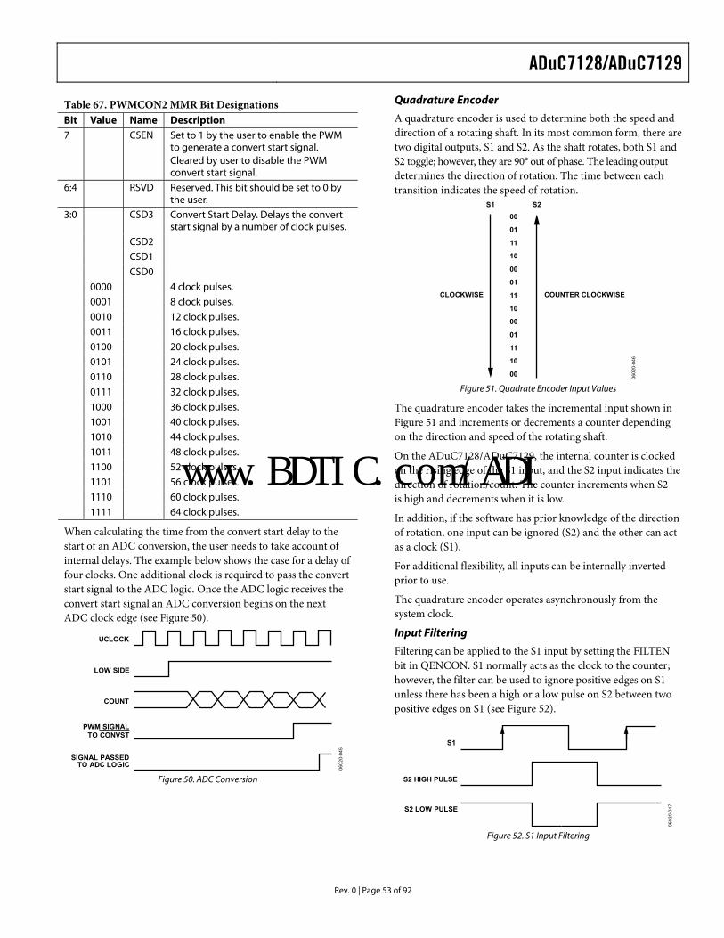
ADuC7128/ADuC7129
Rev. 0 | Page 53 of 92
Table 67. PWMCON2 MMR Bit Designations Bit Value Name Description 7 CSEN Set to 1 by the user to enable the PWM
to generate a convert start signal. Cleared by user to disable the PWM convert start signal.
6:4 RSVD Reserved. This bit should be set to 0 by the user.
CSD3 Convert Start Delay. Delays the convert start signal by a number of clock pulses.
CSD2 CSD1 CSD0 0000 4 clock pulses. 0001 8 clock pulses. 0010 12 clock pulses. 0011 16 clock pulses. 0100 20 clock pulses. 0101 24 clock pulses. 0110 28 clock pulses. 0111 32 clock pulses. 1000 36 clock pulses. 1001 40 clock pulses. 1010 44 clock pulses. 1011 48 clock pulses. 1100 52 clock pulses. 1101 56 clock pulses. 1110 60 clock pulses.
3:0
1111 64 clock pulses.
When calculating the time from the convert start delay to the start of an ADC conversion, the user needs to take account of internal delays. The example below shows the case for a delay of four clocks. One additional clock is required to pass the convert start signal to the ADC logic. Once the ADC logic receives the convert start signal an ADC conversion begins on the next ADC clock edge (see Figure 50).
UCLOCK
LOW SIDE
COUNT
PWM SIGNAL
SIGNAL PASSEDTO ADC LOGIC
0602
0-04
5
TO CONVST
Figure 50. ADC Conversion
Quadrature Encoder
A quadrature encoder is used to determine both the speed and direction of a rotating shaft. In its most common form, there are two digital outputs, S1 and S2. As the shaft rotates, both S1 and S2 toggle; however, they are 90° out of phase. The leading output determines the direction of rotation. The time between each transition indicates the speed of rotation.
CLOCKWISE COUNTER CLOCKWISE
S1 S200
01
11
10
00
01
11
10
00
01
11
10
00 0602
0-04
6
Figure 51. Quadrate Encoder Input Values
The quadrature encoder takes the incremental input shown in Figure 51 and increments or decrements a counter depending on the direction and speed of the rotating shaft.
On the ADuC7128/ADuC7129, the internal counter is clocked on the rising edge of the S1 input, and the S2 input indicates the direction of rotation/count. The counter increments when S2 is high and decrements when it is low.
In addition, if the software has prior knowledge of the direction of rotation, one input can be ignored (S2) and the other can act as a clock (S1).
For additional flexibility, all inputs can be internally inverted prior to use.
The quadrature encoder operates asynchronously from the system clock.
Input Filtering
Filtering can be applied to the S1 input by setting the FILTEN bit in QENCON. S1 normally acts as the clock to the counter; however, the filter can be used to ignore positive edges on S1 unless there has been a high or a low pulse on S2 between two positive edges on S1 (see Figure 52).
S1
S2 HIGH PULSE
S2 LOW PULSE
0602
0-04
7
Figure 52. S1 Input Filtering
www.BDTIC.com/ADI
ADuC7128/ADuC7129
Rev. 0 | Page 54 of 92
Table 68. QENCON MMR Bit Designations Bit Name Description 15:11 RSVD Reserved. 10 FILTEN Set to 1 by the user to enable filtering on the S1 pin.
Cleared by user to disable filtering on the S1 pin. 9 RSVD Reserved. This bit should be set to 0 by the user. 8 S2INV Set to 1 by the user to invert the S2 input.
Cleared by user to use the S2 input as normal. If the DIRCON bit is set, then S2INV controls the direction of the counter.
In this case, set to 1 by the user to operate the counter in increment mode. Cleared by user to operate the counter in decrement mode.
7 S1INV Set to 1 by the user to invert the S1 input. Cleared by user to use the S1 input as normal.
6 DIRCON Direction Control. Set to 1 by the user to enable S1 as the input to the counter clock. The direction of the counter is controlled via the S2INV bit. Cleared by user to operate in normal mode.
5 S1IRQEN Set to 1 by the user to generate an IRQ when a low-to-high transition is detected on S1. Cleared by the user to disable the interrupt.
4 RSVD This bit should be set to 0 by the user. 3 UIRQEN Underflow IRQ Enable.
Set to 1 by the user to generate an interrupt if QENVAL underflows. Cleared by the user to disable the interrupt.
2 OIREQEN Overflow IRQ Enable. Set to 1 by the user to generate an interrupt if QENVAL overflows. Cleared by user to disable the interrupt.
1 RSVD This bit should be set to 0 by the user. 0 ENQEN Quadrature Encoder Enable.
Set to 1 by the user to enable the quadrature encoder. Cleared by user to disable the quadrature encoder.
Table 69. QENSTA MMR Bit Designations Bit Name Description 7:5 RSVD Reserved. 4 S1EDGE S1 Rising Edge.
This bit is set automatically on a rising edge of S1. Cleared by reading QENSTA.
3 RSVD Reserved. 2 UNDER Underflow Flag.
This bit is set automatically if an underflow occurs. Cleared by reading QENSTA.
1 OVER This bit is set automatically if an overflow has occurred. Cleared by reading QENSTA.
0 DIR Direction of the Counter. Set to 1 by hardware to indicate that the counter is incrementing. Set to 0 by hardware to indicate that the counter is decrementing.
QENDAT Register Name Address Default Value Access QENDAT 0xFFFF0F08 0Xffff R/W
The QENDAT register holds the maximum value allowed for the QENVAL register. If the QENVAL register increments past the value in this register, an overflow condition occurs. When an over-flow occurs, the QENVAL register is reset to 0x0000. When the QENVAL register decrements past zero during an underflow, it is loaded with the value in QENDAT.
QENVAL Register Name Address Default Value Access QENVAL 0xFFFF0F0C 0x0000 R/W
The QENVAL register contains the current value of the quadrature encoder counter.
www.BDTIC.com/ADI
ADuC7128/ADuC7129
Rev. 0 | Page 55 of 92
QENCLR Register Name Address Default Value Access QENCLR 0xFFFF0F14 0x00000000 R/W
Writing any value to the QENCLR register clears the QENVAL register to 0x0000. The bits in this register are undefined.
QENSET Register Name Address Default Value Access QENSET 0xFFFF0F18 0x00000000 R/W
Writing any value to the QENSET register loads the QENVAL register with the value in QENDAT. The bits in this register are undefined.
Note that the interrupt conditions are OR’ed together to form one interrupt to the interrupt controller. The interrupt service routine should check the QENSTA register to find out the cause of the interrupt.
• The S1 and S2 inputs appear as the QENS1 and QENS2 inputs in the GPIO list.
• The motor speed can be measured by using the capture facility in Timer0 or Timer1.
• An overflow of either timer can be checked by using an ISR or by checking IRQSIG.
The counter with the quadrature encoder is gray encoded to ensure reliable data transfer across clock boundaries. When an underflow or overflow occur, the count value does not jump to the other end of the scale; instead, the direction of count changes. When this happens, the value in QENDAT is subtracted from the value derived from the gray count.
When the value in QENDAT changes, the value read back from QENVAL changes. However, the gray encoded value does not change. This only occurs after an underflow or overflow. If the value in QENDAT changes, there must be a write to QENSET or QENCLR to ensure a valid number is read back from QENVAL.
GENERAL-PURPOSE I/O The ADuC7128/ADuC7129 provide 40 general-purpose, bidirectional I/O (GPIO) pins. All I/O pins are 5 V tolerant, meaning that the GPIOs support an input voltage of 5 V. In general, many of the GPIO pins have multiple functions (see Table 70). By default, the GPIO pins are configured in GPIO mode.
All GPIO pins have an internal pull-up resistor (of about 100 kΩ) and their drive capability is 1.6 mA. Note that a maximum of 20 GPIO can drive 1.6 mA at the same time. The following GPIOs have programmable pull-up: P0.0, P0.4, P0.5, P0.6, P0.7, and the eight GPIOs of P1.
The 40 GPIOs are grouped in five ports: Port 0 to Port 4. Each port is controlled by four or five MMRs, with x representing the port number.
GPxCON Register Name Address Default Value Access GP0CON 0xFFFF0D00 0x00000000 R/W GP1CON 0xFFFF0D04 0x00000000 R/W GP2CON 0xFFFF0D08 0x00000000 R/W GP3CON 0xFFFF0D0C 0x11111111 R/W GP4CON 0xFFFF0D10 0x00000000 R/W
Note that the kernel changes P0.6 from its default configuration at reset (MRST) to GPIO mode. If MRST is used for external circuitry, an external pull-up resistor should be used to ensure that the level on P0.6 does not drop when the kernel switches mode. Otherwise, P0.6 goes low for the reset period. For example, if MRST is required for power-down, it can be reconfigured in GP0CON MMR.
The input level of any GPIO can be read at any time in the GPxDAT MMR, even when the pin is configured in a mode other than GPIO. The PLA input is always active. When the ADuC7128/ADuC7129 enter a power-saving mode, the GPIO pins retain their state. GPxCON is the Port x control register, and it selects the function of each pin of Port x, as described in Table 70.
www.BDTIC.com/ADI
ADuC7128/ADuC7129
Rev. 0 | Page 56 of 92
Table 70. GPIO Pin Function Designations Configuration Port Pin 00 01 10 11 0 P0.0 GPIO CMP MS0 PLAI[7] P0.11 GPIO BLE - P0.21 GPIO BHE P0.3 GPIO TRST A16 ADC BBUSYB
P0.4 GPIO/IRQ0 CONVST MS1 PLAO[1]
P0.5 GPIO/IRQ1 ADCBUSY PLM_COMP PLAO[2] P0.6 GPIO/T1 MRST AE PLAO[3]
P0.7 GPIO ECLK/XCLK2P SIN0 PLAO[4]
1 P1.0 GPIO/T1 SIN0 SCL0 PLAI[0] P1.1 GPIO SOUT0 SDA0 PLAI[1] P1.2 GPIO RTS0 SCL1 PLAI[2] P1.3 GPIO CTS0 SDA1 PLAI[3] P1.4 GPIO/IRQ2 RI0 CLK PLAI[4] P1.5 GPIO/IRQ3 DCD0 MISO PLAI[5] P1.6 GPIO DSR0 MOSI PLAI[6] P1.7 GPIO DTR0 CSL PLAO[0] 2 P2.0 GPIO SYNC SOUT PLAO[5] P2.11 GPIO WS PLAO[6] P2.21 GPIO RTS1 RS PLAO[7] P2.31 GPIO CTS1 AE P2.41 GPIO RI1 MS0 P2.51 GPIO DCD1 MS1 P2.61 GPIO DSR1 MS2 P2.71 GPIO DTR1 MS3 3 P3.0 GPIO PWM1 AD0 PLAI[8] P3.1 GPIO PWM2 AD1 PLAI[9] P3.2 GPIO PWM3 AD2 PLAI[10] P3.3 GPIO PWM4 AD3 PLAI[11] P3.4 GPIO PWM5 AD4 PLAI[12] P3.5 GPIO PWM6 AD5 PLAI[13] P3.61 GPIO PWM1 AD6 PLAI[14] P3.71 GPIO PWM3 AD7 PLAI[15] 4 P4.0 GPIO QENS1 AD8 PLAO[8] P4.1 GPIO QENS2 AD9 PLAO[9] P4.2 GPIO RSVD AD10 PLAO[10] P4.3 GPIO Trip
(Shutdown) AD11 PLAO[11]
P4.4 GPIO PLMIN AD12 PLAO[12] P4.5 GPIO PLMOUT AD13 PLAO[13] P4.6 GPIO SIN1 AD14 PLAO[14] P4.7 GPIO SOUT1 AD15 PLAO[15] 1 Available only on the 80-lead ADuC7129. 2 When configured in Mode 1, PO.7 is ECLK by default, or core clock output. To
configure it as a clock ouput, the MDCLK bits in PLLCON must be set to 11.
Table 71. GPxCON MMR Bit Designations Bit Description 31:30 Reserved 29:28 Select function of Px.7 pin 27:26 Reserved 25:24 Select function of Px.6 pin 23:22 Reserved 21:20 Select function of Px.5 pin 19:18 Reserved 17:16 Select function of Px.4 pin 15:14 Reserved 13:12 Select function of Px.3 pin 11:10 Reserved 9:8 Select function of Px.2 pin 7:6 Reserved 5:4 Select function of Px.1 pin 3:2 Reserved 1:0 Select function of Px.0 pin
GPxPAR Register Name Address Default Value Access GP0PAR 0xFFFF0D2C 0x20000000 R/W GP1PAR 0xFFFF0D3C 0x00000000 R/W GP3PAR 0xFFFF0D5C 0x00222222 R/W GP4PAR 0xFFFF0D6C 0x00000000 R/W
GPxPAR programs the parameters for Port 0, Port 1, Port 3, and Port 4. Note that the GPxDAT MMR must always be written after changing the GPxPAR MMR.
Table 72. GPxPAR MMR Bit Designations Bit Description 31:29 Reserved 28 Pull-up disable Px.7 pin 27:25 Reserved 24 Pull-up disable Px.6 pin 23:21 Reserved 20 Pull-up disable Px.5 pin 19:17 Reserved 16 Pull-up disable Px.4 pin 15:13 Reserved 12 Pull-up disable Px.3 pin 11:9 Reserved 8 Pull-up disable Px.2 pin 7:5 Reserved 4 Pull-up disable Px.1 pin 3:1 Reserved 0 Pull-up disable Px.0 pin
www.BDTIC.com/ADI
ADuC7128/ADuC7129
Rev. 0 | Page 57 of 92
GPxDAT Register Name Address Default Value Access GP0DAT 0xFFFF0D20 0x000000XX R/W GP1DAT 0xFFFF0D30 0x000000XX R/W GP2DAT 0xFFFF0D40 0x000000XX R/W GP3DAT 0xFFFF0D50 0x000000XX R/W GP4DAT 0xFFFF0D60 0x000000XX R/W
GPxDAT is a Port x configuration and data register. It configures the direction of the GPIO pins of Port x, sets the output value for the pins configured as output, and receives and stores the input value of the pins configured as input.
Table 73. GPxDAT MMR Bit Designations Bit Description 31:24 Direction of the Data.
Set to 1 by user to configure the GPIO pins as outputs. Cleared to 0 by user to configure the GPIO pins as inputs.
23:16 Port x Data Output. 15:8 Reflect the state of Port x pins at reset (read only). 7:0 Port x Data Input (Read Only).
GPxSET Register Name Address Default Value Access GP0SET 0xFFFF0D24 0x000000XX W GP1SET 0xFFFF0D34 0x000000XX W GP2SET 0xFFFF0D44 0x000000XX W GP3SET 0xFFFF0D54 0x000000XX W GP4SET 0xFFFF0D64 0x000000XX W
GPxSET is a data set Port x register.
Table 74. GPxSET MMR Bit Designations Bit Description 31:24 Reserved. 23:16 Data Port x Set Bit.
Set to 1 by user to set bit on Port x; also sets the corresponding bit in the GPxDAT MMR. Cleared to 0 by user; does not affect the data out.
15:0 Reserved.
GPxCLR Register Name Address Default Value Access GP0CLR 0xFFFF0D28 0x000000XX W GP1CLR 0xFFFF0D38 0x000000XX W GP2CLR 0xFFFF0D48 0x000000XX W GP3CLR 0xFFFF0D58 0x000000XX W GP4CLR 0xFFFF0D68 0x000000XX W
GPxCLR is a data clear Port x register.
Table 75. GPxCLR MMR Bit Designations Bit Description 31:24 Reserved. 23:16 Data Port x Clear Bit.
Set to 1 by user to clear bit on Port x; also clears the corresponding bit in the GPxDAT MMR. Cleared to 0 by user; does not affect the data out.
15:0 Reserved.
SERIAL PORT MUX The serial port mux multiplexes the serial port peripherals (two I2Cs, an SPI, and two UARTs) and the programmable logic array (PLA) to a set of 10 GPIO pins. Each pin must be configured to its specific I/O function as described in Table 76.
Table 76. SPM Configuration
Pin GPIO (00)
UART (01)
UART/I2C/SPI (10)
PLA (11)
SPM0 P1.0 SIN0 I2C0SCL PLAI[0]
SPM1 P1.1 SOUT0 I2C0SDA PLAI[1]
SPM2 P1.2 RTS0 I2C1SCL PLAI[2]
SPM3 P1.3 CTS0 I2C1SDA PLAI[3]
SPM4 P1.4 RI0 SPICLK PLAI[4]
SPM5 P1.5 DCD0 SPIMISO PLAI[5]
SPM6 P1.6 DSR0 SPIMOSI PLAI[6]
SPM7 P1.7 DTR0 SPICSL PLAO[0]
SPM8 P0.7 ECLK SIN0 PLAO[4]
SPM9 P2.01 PWMSYNC SOUT0 PLAO[5]
SPM10 P2.21 RTS1 RS PLAO[7]
SPM11 P2.31 CTS1 AE
SPM12 P2.41 RI1 MS0
SPM13 P2.51 DCD1 MS1
SPM14 P2.61 DSR1 MS2
SPM15 P2.71 DTR1 MS3
SPM16 P4.6 SIN1 AD14 PLAO[14]
SPM17 P4.7 SOUT1 AD15 PLAO[15]
1 Available only on the 80-lead ADuC7129.
Table 76 details the mode for each of the SPMUX GPIO pins. This configuration has to be performed via the GP0CON, GP1CON and GP2CON MMRs. By default these pins are configured as GPIOs.
UART SERIAL INTERFACE The ADuC7128/ADuC7129 contain two identical UART blocks. Although only UART0 is described here, UART1 functions in exactly the same way.
The UART peripheral is a full-duplex universal asynchronous receiver/transmitter, fully compatible with the 16450 serial port standard.
The UART performs serial-to-parallel conversion on data characters received from a peripheral device or a modem, and parallel-to-serial conversion on data characters received from the CPU. The UART includes a fractional divider for baud rate generation and has a network-addressable mode. The UART function is made available on 10 pins of the ADuC7128/ ADuC7129 (see Table 77).
www.BDTIC.com/ADI
ADuC7128/ADuC7129
Rev. 0 | Page 58 of 92
Table 77. UART Signal Descriptions Pin Signal Description SPM0 (Mode 1) SIN0 Serial Receive Data. SPM1 (Mode 1) SOUT0 Serial Transmit Data. SPM2 (Mode 1) RTS0 Request to Send. SPM3 (Mode 1) CTS0 Clear to Send. SPM4 (Mode 1) RI0 Ring Indicator. SPM5 (Mode 1) DCD0 Data Carrier Detect. SPM6 (Mode 1) DSR0 Data Set Ready. SPM7 (Mode 1) DTR0 Data Terminal Ready. SPM8 (Mode 2) SIN0 Serial Receive Data. SPM9 (Mode 2) SOUT0 Serial Transmit Data.
The serial communication adopts an asynchronous protocol that supports various word-length, stop-bits, and parity generation options selectable in the configuration register.
Baud Rate Generation
There are two ways of generating the UART baud rate: normal 450 UART baud rate generation and using the fractional divider.
Normal 450 UART Baud Rate Generation
The baud rate is a divided version of the core clock, using the value in COM0DIV0 and COM0DIV1 MMRs (16-bit value, DL).
DLRateBaud CD ×××
=2162
MHz78.41
Table 78 gives some common baud rate values.
Table 78. Baud Rate Using the Normal Baud Rate Generator Baud Rate CD DL Actual Baud Rate % Error 9600 0 0x88 9600 0% 19,200 0 0x44 19,200 0% 115,200 0 0x0B 118,691 3% 9600 3 0x11 9600 0% 19,200 3 0x08 20,400 6.25% 115,200 3 0x01 163,200 41.67%
Using the Fractional Divider
The fractional divider combined with the normal baud rate generator allows the generating of a wider range of more accurate baud rates.
/16DL UART
FBENCORECLOCK /2
/(M + N/2048)
0602
0-04
8
Figure 53. Baud Rate Generation Options
Calculation of the baud rate using fractional divider is as follows:
)2048
(2162
MHz78.41NMDL
RateBaudCD +××××
=
2162MHz78.41
2048 ××××=+
DLRateBaudN
M CD
For example, generation of 19,200 bauds with CD bits = 3. Table 78 gives DL = 0x08.
2816219200MHz78.41
2048 3 ××××=+
NM
06.12048
=+NM
where: M = 1 N = 0.06 × 2048 = 128
( )2048128
28162
MHz78.413 ××××
=RateBaud
where: Baud Rate = 19,200 bps. Error = 0% compared to 6.25% with the normal baud rate generator.
UART Register Definitions
The UART interface consists of 12 registers.
Table 79. UART MMRs Register Description
COMxTX 8-Bit Transmit Register. COMxRX 8-Bit Receive Register. COMxDIV0 Divisor Latch (Low Byte). COMxTX, COMxRX, and COMxDIV0
Share The Same Address Location. COMxTX and COMxRX can be accessed when Bit 7 in COMxCON0 register is cleared. COMxDIV0 can be accessed when Bit 7 of COMxCON0 is set.
COMxDIV1 Divisor Latch (High Byte). COMxCON0 Line Control Register. COMxSTA0 Line Status Register. COMxIEN0 Interrupt Enable Register. COMxIID0 Interrupt Identification Register. COMxCON1 Modem Control Register. COMxSTA1 Modem Status Register. COMxDIV2 16-Bit Fractional Baud Divide Register. COMxSCR 8-Bit Scratch Register Used for
Temporary Storage. Also used in network addressable UART mode.
www.BDTIC.com/ADI
ADuC7128/ADuC7129
Rev. 0 | Page 59 of 92
Table 80. COMxCON0 MMR Bit Designations Bit Value Name Description 7 DLAB Divisor Latch Access.
Set by user to enable access to COMxDIV0 and COMxDIV1 registers. Cleared by user to disable access to COMxDIV0 and COMxDIV1 and enable access to COMxRX and COMxTX.
6 BRK Set Break. Set by user to force SOUT to 0. Cleared to operate in normal mode.
5 SP Stick Parity. Set by user to force parity to defined values.
1 if EPS = 1 and PEN = 1 0 if EPS = 0 and PEN = 1
4 EPS Even Parity Select Bit. Set for even parity. Cleared for odd parity.
3 PEN Parity Enable Bit. Set by user to transmit and check the parity bit. Cleared by user for no parity transmission or checking.
2 STOP Stop Bit. Set by user to transmit 1.5 stop bits if the word length is 5 bits or 2 stop bits if the word length is 6 bits, 7 bits, or 8 bits. The receiver checks the first stop bit only, regardless of the number of stop bits selected. Cleared by user to generate 1 stop bit in the transmitted data.
1:0 WLS Word Length Select. 00 5 bits. 01 6 bits. 10 7 bits. 11 8 bits.
Table 81. COMxSTA0 MMR Bit Designations Bit Name Description 7 RSVD Reserved. 6 TEMT COMxTX Empty Status Bit.
Set automatically if COMxTX is empty. Cleared automatically when writing to COMxTX.
5 THRE COMxTX and COMxRX Empty. Set automatically if COMxTX and COMxRX are empty. Cleared automatically when one of the registers receives data.
4 BI Break Error. Set when SIN is held low for more than the maximum word length. Cleared automatically.
3 FE Framing Error. Set when stop bit invalid. Cleared automatically.
2 PE Parity Error. Set when a parity error occurs. Cleared automatically.
1 OE Overrun Error. Set automatically if data is overwritten before it is read. Cleared automatically.
0 DR Data Ready. Set automatically when COMxRX is full. Cleared by reading COMxRX.
www.BDTIC.com/ADI
ADuC7128/ADuC7129
Rev. 0 | Page 60 of 92
Table 82. COMxIEN0 MMR Bit Designations Bit Name Description 7:4 RSVD Reserved. 3 EDSSI Modem Status Interrupt Enable Bit.
Set by user to enable generation of an interrupt if any of COMxSTA1[3:0] are set. Cleared by user.
2 ELSI RX Status Interrupt Enable Bit. Set by user to enable generation of an interrupt if any of COMxSTA0[3:1] are set. Cleared by user.
1 ETBEI Enable Transmit Buffer Empty Interrupt. Set by user to enable interrupt when buffer is empty during a transmission. Cleared by user.
0 ERBFI Enable Receive Buffer Full Interrupt. Set by user to enable interrupt when buffer is full during a reception. Cleared by user.
Table 83. COMxIID0 MMR Bit Designations Bit 2:1 Status Bits
Bit 0 NINT Priority Definition Clearing Operation
00 1 No Interrupt. 11 0 1 Receive Line Status Interrupt. Read COMxSTA0. 10 0 2 Receive Buffer Full Interrupt. Read COMxRX. 01 0 3 Transmit Buffer Empty Interrupt. Write data to COMxTX or read COMxIID0. 00 0 4 Modem Status Interrupt. Read COMxSTA1.
Table 84. COMxCON1 MMR Bit Designations Bit Name Description 7:5 RSVD Reserved. 4 LOOPBACK Loop Back.
Set by user to enable loop-back mode. In loop-back mode, the SOUT is forced high. In addition, the modem signals are directly connected to the status inputs (RTS to CTS, DTR to DSR, OUT1 to RI, and OUT2 to DCD).
3 Reserved. 2 Reserved. 1 RTS Request to Send.
Set by user to force the RTS output to 0. Cleared by user to force the RTS output to 1.
0 DTR Data Terminal Ready. Set by user to force the DTR output to 0. Cleared by user to force the DTR output to 1.
www.BDTIC.com/ADI
ADuC7128/ADuC7129
Rev. 0 | Page 61 of 92
Table 85. COMxSTA1 MMR Bit Designations Bit Name Description 7 DCD Data Carrier Detect. 6 RI Ring Indicator. 5 DSR Data Set Ready. 4 CTS Clear to Send. 3 DDCD Delta Data Carrier Detect.
Set automatically if DCD changed state since COMxSTA1 last read. Cleared automatically by reading COMxSTA1.
2 TERI Trailing Edge Ring Indicator. Set if NRI changed from 0 to 1 since COMxSTA1 last read. Cleared automatically by reading COMxSTA1.
1 DDSR Delta Data Set Ready. Set automatically if DSR changed state since COMxSTA1 last read. Cleared automatically by reading COMxSTA1.
0 DCTS Delta Clear to Send. Set automatically if CTS changed state since COMxSTA1 last read. Cleared automatically by reading COMxSTA1.
Table 86. COMxDIV2 MMR Bit Designations Bit Name Description 15 FBEN Fractional Baud Rate Generator Enable Bit.
Set by user to enable the fractional baud rate generator. Cleared by user to generate baud rate using the standard 450 UART baud rate generator.
14:13 RSVD Reserved. 12:11 FBM[1 to 0] M, if FBM = 0, M = 4 (see the Using the Fractional Divider section). 10:0 FBN[10 to 0] N (see the Using the Fractional Divider section).
Network Addressable UART Mode
This mode allows connecting the MicroConverter on a 256-node serial network, either as a hardware single master or via software in a multimaster network. Bit 7 of COMxIEN1 (ENAM bit) must be set to enable UART in network-addressable mode.
Note that there is no parity check in this mode. The parity bit is used for address.
Network Addressable UART Register Definitions
Four additional registers, COMxIEN0, COMxIEN1, COMxIID1, and COMxADR are used only in network addressable UART mode.
In network address mode, the least significant bit of the COMxIEN1 register is the transmitted network address control bit. If set to 1, the device is transmitting an address. If cleared to 0, the device is transmitting data. For example, the following master-based code transmits the slave address followed by the data:
COM0IEN1 = 0xE7; //Setting ENAM, E9BT, E9BR, ETD, NABP
COM0TX = 0xA0; // Slave address is 0xA0
while(!(0x020==(COM0STA0 & 0x020))) // wait for adr tx to finish.
COM0IEN1 = 0xE6; // Clear NAB bit to indicate Data is coming
COM0TX = 0x55; // Tx data to slave: 0x55
www.BDTIC.com/ADI
ADuC702x Series Preliminary Technical Data
Rev. 0 | Page 62 of 92
Table 87. COMxIEN1 MMR Bit Designations
Table 88. COMxIID1 MMR Bit Designations Bit 3:1 Status Bits
Bit 0 NINT Priority Definition Clearing Operation
000 1 No Interrupt. 110 0 2 Matching Network Address. Read COMxRX. 101 0 3 Address Transmitted, Buffer Empty. Write data to COMxTX or read COMxIID0. 011 0 1 Receive Line Status Interrupt. Read COMxSTA0. 010 0 2 Receive Buffer Full Interrupt. Read COMxRX. 001 0 3 Transmit Buffer Empty Interrupt. Write data to COMxTX or read COMxIID0. 000 0 4 Modem Status Interrupt. Read COMxSTA1 register.
Note that to receive a network address interrupt, the slave must ensure that Bit 0 of COMxIEN0 (enable receive buffer full interrupt) is set to 1.
COMxADR is an 8-bit, read/write network address register that holds the address checked for by the network addressable UART. Upon receiving this address, the device interrupts the processor and/or sets the appropriate status bit in COMxIID1.
Bit Name Description 7 ENAM Network Address Mode Enable Bit.
Set by user to enable network address mode. Cleared by user to disable network address mode.
6 E9BT 9-Bit Transmit Enable Bit. Set by user to enable 9-bit transmit. ENAM must be set. Cleared by user to disable 9-bit transmit.
5 E9BR 9-Bit Receive Enable Bit. Set by user to enable 9-bit receive. ENAM must be set. Cleared by user to disable 9-bit receive.
4 ENI Network Interrupt Enable Bit. 3 E9BD Word Length.
Set for 9-bit data. E9BT has to be cleared. Cleared for 8-bit data.
2 ETD Transmitter Pin Driver Enable Bit. Set by user to enable SOUT as an output in slave mode or multimaster mode. Cleared by user; SOUT is three-state.
1 NABP Network Address Bit, Interrupt Polarity Bit. 0 NAB Network Address Bit.
Set by user to transmit the slave’s address. Cleared by user to transmit data.
www.BDTIC.com/ADI
ADuC7128/ADuC7129
Rev. 0 | Page 63 of 92
SERIAL PERIPHERAL INTERFACE The ADuC7128/ADuC7129 integrate a complete hardware serial peripheral interface (SPI) on-chip. SPI is an industry-standard synchronous serial interface that allows eight bits of data to be synchronously transmitted and simultaneously received, that is, full duplex up to a maximum bit rate of 3.4 Mbs. The SPI interface is operational only with core clock divider bits POWCON[2:0] = 0, 1, or 2.
The SPI port can be configured for master or slave operation and typically consists of four pins, namely: MISO, MOSI, SCL, and CS.
MISO (Master In, Slave Out) Data I/O Pin
The MISO pin is configured as an input line in master mode and an output line in slave mode. The MISO line on the master (data in) should be connected to the MISO line in the slave device (data out). The data is transferred as byte wide (8-bit) serial data, MSB first.
MOSI (Master Out, Slave In) Pin
The MOSI pin is configured as an output line in master mode and an input line in slave mode. The MOSI line on the master (data out) should be connected to the MOSI line in the slave device (data in). The data is transferred as byte wide (8-bit) serial data, MSB first.
SCL (Serial Clock) I/O Pin
The master serial clock (SCL) is used to synchronize the data being transmitted and received through the MOSI SCL period. Therefore, a byte is transmitted/received after eight SCL periods. The SCL pin is configured as an output in master mode and as an input in slave mode.
In master mode, polarity and phase of the clock are controlled by the SPICON register, and the bit rate is defined in the SPIDIV register as follows:
)1(2 SPIDIVf
f HCLKCLOCKSERIAL +×
=
In slave mode, the SPICON register must be configured with the phase and polarity of the expected input clock. The slave accepts data from an external master up to 3.4 Mbs at CD = 0.
In both master and slave modes, data is transmitted on one edge of the SCL signal and sampled on the other. Therefore, it is important that the polarity and phase be configured the same for the master and slave devices.
The maximum speed of the SPI clock is dependent on the clock divider bits and is summarized in Table 89.
Table 89. SPI Speed vs. Clock Divider Bits in Master Mode CD Bits 0 1 2 3 4 5 SPIDIV in hex 0x05 0x0B 0x17 0x2F 0x5F 0xBF SPI speed
in MHz 3.482 1.741 0.870 0.435 0.218 0.109
In slave mode, the SPICON register must be configured with the phase and polarity of the expected input clock. The slave accepts data from an external master up to 10.4 Mbs at CD = 0. The formula to determine the maximum speed follows:
4HCLK
CLOCKSERIALf
f =
In both master and slave modes, data is transmitted on one edge of the SCL signal and sampled on the other. Therefore, it is important that the polarity and phase be configured the same for the master and slave devices.
Chip Select (CS) Input Pin
In SPI slave mode, a transfer is initiated by the assertion of CS, which is an active low input signal. The SPI port then transmits and receives 8-bit data until the transfer is concluded by desassertion of CS. In slave mode, CS is always an input.
SPI Registers
The following MMR registers are used to control the SPI interface: SPISTA, SPIRX, SPITX, SPIDIV, and SPICON.
SPISTA Register Name Address Default Value Access SPISTA 0xFFFF0A00 0x00 R
SPISTA is an 8-bit read-only status register.
Table 90. SPISTA MMR Bit Designations Bit Description 7:6 Reserved. 5 SPIRX Data Register Overflow Status Bit.
Set if SPIRX is overflowing. Cleared by reading SPIRX register.
4 SPIRX Data Register IRQ. Set automatically if Bit 3 or Bit 5 is set. Cleared by reading SPIRX register.
3 SPIRX Data Register Full Status Bit. Set automatically if valid data is present in the SPIRX register. Cleared by reading SPIRX register.
2 SPITX Data Register Underflow Status Bit. Set automatically if SPITX is underflowing. Cleared by writing in the SPITX register.
1 SPITX Data Register IRQ. Set automatically if Bit 0 is clear or Bit 2 is set. Cleared by writing in the SPITX register or if finished transmission disabling the SPI.
0 SPITX Data Register Empty Status Bit. Set by writing to SPITX to send data. This bit is set during transmission of data. Cleared when SPITX is empty.
www.BDTIC.com/ADI
ADuC7128/ADuC7129
Rev. 0 | Page 64 of 92
SPIRX Register Name Address Default Value Access SPIRX 0xFFFF0A04 0x00 R
SPIRX is an 8-bit read-only receive register.
SPITX Register Name Address Default Value Access SPITX 0xFFFF0A08 0x00 W
SPITX is an 8-bit write-only transmit register.
SPIDIV Register Name Address Default Value Access SPIDIV 0xFFFF0A0C 0x1B R/W
SPIDIV is an 8-bit serial clock divider register.
SPICON Register Name Address Default Value Access SPICON 0xFFFF0A10 0x0000 R/W
SPICON is a 16-bit control register.
Table 91. SPICON MMR Bit Designations Bit Description 15:13 Reserved. 12 Continuous Transfer Enable.
Set by user to enable continuous transfer. In master mode, the transfer continues until no valid data is available in the TX register. CS is asserted and remains asserted for the duration of each 8-bit serial transfer until TX is empty. Cleared by user to disable continuous transfer. Each transfer consists of a single 8-bit serial transfer. If valid data exists in the SPITX register, then a new transfer is initiated after a stall period.
11 Loopback Enable. Set by user to connect MISO to MOSI and test software. Cleared by user to be in normal mode.
10 Slave Output Enable. Set by user to enable the slave output. Cleared by user to disable slave output.
9 Slave Select Input Enable. Set by user in master mode to enable the output.
8 SPIRX Overflow Overwrite Enable. Set by user, the valid data in the RX register is overwritten by the new serial byte received. Cleared by user, the new serial byte received is discarded.
7 SPITX Underflow Mode. Set by user to transmit 0. Cleared by user to transmit the previous data.
6 Transfer and Interrupt Mode (Master Mode). Set by user to initiate transfer with a write to the SPITX register. Interrupt occurs when TX is empty. Cleared by user to initiate transfer with a read of the SPIRX register. Interrupt occurs when RX is full.
5 LSB First Transfer Enable Bit. Set by user, the LSB is transmitted first. Cleared by user, the MSB is transmitted first.
4 Reserved. Should be set to 0. 3 Serial Clock Polarity Mode Bit.
Set by user, the serial clock idles high. Cleared by user, the serial clock idles low.
2 Serial Clock Phase Mode Bit. Set by user, the serial clock pulses at the beginning of each serial bit transfer. Cleared by user, the serial clock pulses at the end of each serial bit transfer.
1 Master Mode Enable Bit. Set by user to enable master mode. Cleared by user to enable slave mode.
0 SPI Enable Bit. Set by user to enable the SPI. Cleared to disable the SPI.
www.BDTIC.com/ADI
ADuC7128/ADuC7129
Rev. 0 | Page 65 of 92
I2C-COMPATIBLE INTERFACES The ADuC7128/ADuC7129 support two fully licensed I2C interfaces. The I2C interfaces are both implemented as full hardware master and slave interfaces. Because the two I2C interfaces are identical, only I2C0 is described in detail. Note that the two masters and slaves have individual interrupts.
Note that when configured as an I2C master device, the ADuC7128/ADuC7129 cannot generate a repeated start condition.
The two pins used for data transfer, SDA and SCL, are configured in a wire-AND’ed format that allows arbitration in a multimaster system. These pins require external pull-up resistors. Typical pull-up values are 10 kΩ.
The I2C bus peripheral addresses in the I2C bus system are programmed by the user. This ID can be modified any time a transfer is not in progress. The user can configure the interface to respond to four slave addresses.
The transfer sequence of an I2C system consists of a master device initiating a transfer by generating a start condition while the bus is idle. The master transmits the address of the slave device and the direction of the data transfer in the initial address transfer. If the master does not lose arbitration and the slave acknowledges, then the data transfer is initiated. This continues until the master issues a stop condition and the bus becomes idle.
The I2C peripheral master and slave functionality are independent and can be simultaneously active. A slave is activated when a transfer has been initiated on the bus.
If it is not addressed, it remains inactive until another transfer is initiated. This also allows a master device, which has lost arbitration, to respond as a slave in the same cycle.
Serial Clock Generation
The I2C master in the system generates the serial clock for a transfer. The master channel can be configured to operate in fast mode (400 kHz) or standard mode (100 kHz).
The bit rate is defined in the I2C0DIV MMR as follows:
) (2 )2( DIVLDIVH +++= UCLK
CLOCKERIALSf
f
where: fUCLK is the clock before the clock divider. DIVH is the high period of the clock. DIVL is the low period of the clock.
Thus, for 100 kHz operation
DIVH = DIVL = 0xCF
and for 400 kHz
DIVH = 0x28 DIVL = 0x3C.
The I2CxDIV register corresponds to DIVH:DIVL.
Slave Addresses
Register I2C0ID0, Register I2C0ID1, Register I2C0ID2, and Register I2C0ID3 contain the device IDs. The device compares the four I2C0IDx registers to the address byte. The seven most significant bits of either ID register must be identical to that of the seven most significant bits of the first address byte received to be correctly addressed. The LSB of the ID registers, transfer direction bit, is ignored in the process of address recognition.
I2C REGISTERS The I2C peripheral interface consists of 18 MMRs that are discussed in this section.
I2CxMSTA Register Name Address Default Value Access I2C0MSTA 0xFFFF0800 0x00 R I2C1MSTA 0xFFFF0900 0x00 R
I2CxMSTA is a status register for the master channel.
Table 92. I2C0MSTA MMR Bit Designations Bit Description 7 Master Transmit FIFO Flush.
Set by user to flush the master Tx FIFO. Cleared automatically once the master Tx FIFO is flushed. This bit also flushes the slave receive FIFO.
6 Master Busy. Set automatically if the master is busy. Cleared automatically.
5 Arbitration Loss. Set in multimaster mode if another master has the bus. Cleared when the bus becomes available.
4 No Acknowledge. Set automatically if there is no acknowledge of the address by the slave device. Cleared automatically by reading the I2C0MSTA register.
3 Master Receive IRQ. Set after receiving data. Cleared automatically by reading the I2C0MRX register.
2 Master Transmit IRQ. Set at the end of a transmission. Cleared automatically by writing to the I2C0MTX register.
1 Master Transmit FIFO Underflow. Set automatically if the master transmit FIFO is underflowing. Cleared automatically by writing to the I2C0MTX register.
0 Master TX FIFO Not Full. Set automatically if the slave transmit FIFO is not full. Cleared automatically by writing twice to the I2C0STX register.
www.BDTIC.com/ADI
ADuC7128/ADuC7129
Rev. 0 | Page 66 of 92
I2CxSSTA Register Name Address Default Value Access I2C0SSTA 0xFFFF0804 0x01 R I2C1SSTA 0xFFFF0904 0x01 R
I2CxSSTA is a status register for the slave channel.
Table 93. I2CxSSTA MMR Bit Designations Bit Value Description 31:15 Reserved. These bits should be written as 0. 14 START Decode Bit.
Set by hardware if the device receives a valid start and matching address. Cleared by an I2C stop condition or an I2C general call reset.
13 Repeated START Decode Bit. Set by hardware if the device receives a valid repeated start and matching address. Cleared by an I2C stop condition, a read of the I2CxSSTA register, or an I2C general call reset.
12:11 ID Decode Bits. 00 Received Address Matched ID Register 0. 01 Received Address Matched ID Register 1. 10 Received Address Matched ID Register 2. 11 Received Address Matched ID Register 3.
10 Stop After Start And Matching Address Interrupt. Set by hardware if the slave device receives an I2C STOP condition after a previous I2C START condition and matching address. Cleared by a read of the I2CxSSTA register.
9:8 General Call ID. 00 No General Call. 01 General Call Reset and Program Address. 10 General Call Program Address. 11 General Call Matching Alternative ID.
7 General Call Interrupt. Set if the slave device receives a general call of any type. Cleared by setting Bit 8 of the I2CxCFG register. If it is a general call reset, all registers are at their default values. If it is a hardware general call, the Rx FIFO holds the second byte of the general call. This is similar to the I2C0ALT register (unless it is a general call to reprogram the device address). For more details, see the I2C Bus Specification, Version 2.1, Jan. 2000.
6 Slave Busy. Set automatically if the slave is busy. Cleared automatically.
5 No Acknowledge. Set if master asks for data and no data is available. Cleared automatically by reading the I2C0SSTA register.
4 Slave Receive FIFO Overflow. Set automatically if the slave receive FIFO is overflowing. Cleared automatically by reading I2C0SRX register.
3 Slave Receive IRQ. Set after receiving data. Cleared automatically by reading the I2C0SRX register or flushing the FIFO.
2 Slave Transmit IRQ. Set at the end of a transmission. Cleared automatically by writing to the I2C0STX register.
1 Slave Transmit FIFO Underflow. Set automatically if the slave transmit FIFO is underflowing. Cleared automatically by writing to the I2C0STX register.
0 Slave Transmit FIFO Empty. Set automatically if the slave transmit FIFO is empty. Cleared automatically by writing twice to the I2C0STX register.
www.BDTIC.com/ADI
Rev. 0 | Page 67 of 92
I2CxSRX Register Name Address Default Value Access I2C0SRX 0xFFFF0808 0x00 R I2C1SRX 0xFFFF0908 0x00 R
I2CxSRX is a receive register for the slave channel.
I2CxSTX Register Name Address Default Value Access I2C0STX 0xFFFF080C 0x00 W I2C1STX 0xFFFF090C 0x00 W
I2CxSTX is a transmit register for the slave channel.
I2CxMRX Register Name Address Default Value Access
I2C0MRX 0xFFFF0810 0x00 R I2C1MRX 0xFFFF0910 0x00 R
I2CxMRX is a receive register for the master channel.
I2CxMTX Register Name Address Default Value Access I2C0MTX 0xFFFF0814 0x00 W I2C1MTX 0xFFFF0914 0x00 W
I2CxMTX is a transmit register for the master channel.
I2CxCNT Register Name Address Default Value Access I2C0CNT 0xFFFF0818 0x00 R/W I2C1CNT 0xFFFF0918 0x00 R/W
I2CxCNT is a master receive data count register. If a master read transfer sequence is initiated, the I2CxCNT register denotes the number of bytes (−1) to be read from the slave device. By default this counter is 0, which corresponds to the expected one byte.
I2CxADR Register Name Address Default Value Access I2C0ADR 0xFFFF081C 0x00 R/W I2C1ADR 0xFFFF091C 0x00 R/W
I2CxADR is a master address byte register. The I2CxADR value is the device address that the master wants to communicate with. It is automatically transmitted at the start of a master transfer sequence if there is no valid data in the I2CxMTX register when the master enable bit is set.
I2CxBYT Register Name Address Default Value Access I2C0BYT 0xFFFF0824 0x00 R/W I2C1BYT 0xFFFF0924 0x00 R/W
I2CxBYT is a broadcast byte register.
I2CxALT Register Name Address Default Value Access I2C0ALT 0xFFFF0828 0x00 R/W I2C1ALT 0xFFFF0928 0x00 R/W
I2CxALT is a hardware general call ID register used in slave mode.
I2CxCFG Register Name Address Default Value Access I2C0CFG 0xFFFF082C 0x00 R/W I2C1CFG 0xFFFF092C 0x00 R/W
I2CxCFG is a configuration register.
Table 94. I2C0CFG MMR Bit Designations Bit Description 31:15 Reserved. These bits should be written by the user as 0. 14 Enable Stop Interrupt.
Set by user to generate an interrupt upon receiving a stop condition and after receiving a valid start condition and matching address. Cleared by user to disable the generation of an interrupt upon receiving a stop condition.
13 Reserved. This bit should be written by the user as 0. 12 Reserved. This bit should be written by the user as 0. 11 Enable Stretch SCL. Holds SCL low.
Set by user to stretch the SCL line. Cleared by user to disable stretching of the SCL line.
10 Reserved. This bit should be written by the user as 0. 9 Slave Tx FIFO Request Interrupt Enable.
Cleared by user to generate an interrupt request just after the negative edge of the clock for the R/W bit. This allows the user to input data into the slave Tx FIFO if it is empty. At 400 kSPS, and with the core clock running at 41.78 MHz, the user has 45 clock cycles to take appropriate action, taking interrupt latency into account. Set by user to disable the slave Tx FIFO request interrupt.
8 General Call Status Bit Clear. Set by user to clear the general call status bits. Cleared automatically by hardware after the general call status bits have been cleared.
www.BDTIC.com/ADI
ADuC7128/ADuC7129
Rev. 0 | Page 68 of 92
Bit Description 7 Master Serial Clock Enable Bit.
Set by user to enable generation of the serial clock in master mode. Cleared by user to disable serial clock in master mode.
6 Loop-Back Enable Bit. Set by user to internally connect the transition to the reception to test user software. Cleared by user to operate in normal mode.
5 Start Back-Off Disable Bit. Set by user in multimaster mode. If losing arbitration, the master immediately tries to retransmit. Cleared by user to enable start back-off. After losing arbitration, the master waits before trying to retransmit.
4 Hardware General Call Enable. When this bit and Bit 3 are set, and have received a general call (Address 0x00) and a data byte, the device checks the contents of the I2C0ALT against the receive register. If the contents match, the device has received a hardware general call. This is used if a device needs urgent attention from a master device without knowing which master it needs to turn to. This is a “to whom it may concern” call. The ADuC7128/ADuC7129 watch for these addresses. The device that requires attention embeds its own address into the message. All masters listen and the one that can handle the device contacts its slave and acts appropriately. The LSB of the I2C0ALT register should always be written to a 1, as per the I2C January 2000 specification.
3 General Call Enable Bit. Set this bit to enable the slave device to acknowledge an I2C general call, Address 0x00 (write). The device then recognizes a data bit. If it receives a 0x06 (reset and write programmable part of slave address by hardware) as the data byte, the I2C interface resets as per the I2C January 2000 specification. This command can be used to reset an entire I2C system. The general call interrupt status bit sets on any general call. The user must take corrective action by setting up the I2C interface after a reset. If it receives a 0x04 (write programmable part of slave address by hardware) as the data byte, the general call interrupt status bit sets on any general call. The user must take corrective action by reprogramming the device address.
2 Reserved. 1 Master Enable Bit.
Set by user to enable the master I2C channel. Cleared by user to disable the master I2C channel.
0 Slave Enable Bit. Set by user to enable the slave I2C channel. A slave transfer sequence is monitored for the device address in I2C0ID0, I2C0ID1, I2C0ID2, and I2C0ID3. If the device address is recognized, the part participates in the slave transfer sequence. Cleared by user to disable the slave I2C channel.
I2CxDIV Register Name Address Default Value Access I2C0DIV 0xFFFF0830 0x1F1F R/W I2C1DIV 0xFFFF0930 0x1F1F R/W
I2CxDIV are the clock divider registers.
I2CxIDx Register Name Address Default Value Access I2C0ID0 0xFFFF0838 0x00 R/W I2C0ID1 0xFFFF083C 0x00 R/W I2C0ID2 0xFFFF0840 0x00 R/W I2C0ID3 0xFFFF0844 0x00 R/W I2C1ID0 0xFFFF0938 0x00 R/W I2C1ID1 0xFFFF093C 0x00 R/W I2C1ID2 0xFFFF0940 0x00 R/W I2C1ID3 0xFFFF0944 0x00 R/W
I2CxID0, I2CxID1, I2CxID2, and I2CxID3 are slave address device ID registers of I2Cx.
I2CxSSC Register Name Address Default Value Access I2C0SSC 0xFFFF0848 0x01 R/W I2C1SSC 0xFFFF0948 0x01 R/W
I2CxSSC is an 8-bit start/stop generation counter. It holds off SDA low for start and stop conditions.
www.BDTIC.com/ADI
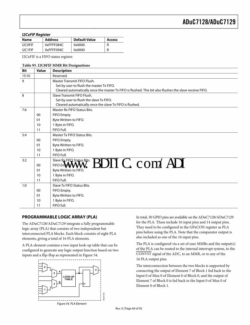
ADuC7128/ADuC7129
Rev. 0 | Page 69 of 92
I2CxFIF Register Name Address Default Value Access I2C0FIF 0xFFFF084C 0x0000 R I2C1FIF 0xFFFF094C 0x0000 R
I2CxFIF is a FIFO status register.
Table 95. I2C0FIF MMR Bit Designations Bit Value Description 15:10 Reserved. 9 Master Transmit FIFO Flush.
Set by user to flush the master Tx FIFO. Cleared automatically once the master Tx FIFO is flushed. This bit also flushes the slave receive FIFO.
8 Slave Transmit FIFO Flush. Set by user to flush the slave Tx FIFO. Cleared automatically once the slave Tx FIFO is flushed.
7:6 Master Rx FIFO Status Bits. 00 FIFO Empty. 01 Byte Written to FIFO. 10 1 Byte in FIFO. 11 FIFO Full. 5:4 Master Tx FIFO Status Bits. 00 FIFO Empty. 01 Byte Written to FIFO. 10 1 Byte in FIFO. 11 FIFO Full. 3:2 Slave Rx FIFO Status Bits. 00 FIFO Empty. 01 Byte Written to FIFO. 10 1 Byte in FIFO. 11 FIFO Full. 1:0 Slave Tx FIFO Status Bits. 00 FIFO Empty. 01 Byte Written to FIFO. 10 1 Byte in FIFO. 11 FIFO full.
PROGRAMMABLE LOGIC ARRAY (PLA) The ADuC7128/ADuC7129 integrate a fully programmable logic array (PLA) that consists of two independent but interconnected PLA blocks. Each block consists of eight PLA elements, giving a total of 16 PLA elements.
A PLA element contains a two input look-up table that can be configured to generate any logic output function based on two inputs and a flip-flop as represented in Figure 54.
42
0
1
3
A
B
LOOK-UPTABLE
0602
0-04
9
Figure 54. PLA Element
In total, 30 GPIO pins are available on the ADuC7128/ADuC7129 for the PLA. These include 16 input pins and 14 output pins. They need to be configured in the GPxCON register as PLA pins before using the PLA. Note that the comparator output is also included as one of the 16 input pins.
The PLA is configured via a set of user MMRs and the output(s) of the PLA can be routed to the internal interrupt system, to the CONVST signal of the ADC, to an MMR, or to any of the 16 PLA output pins.
The interconnection between the two blocks is supported by connecting the output of Element 7 of Block 1 fed back to the Input 0 of Mux 0 of Element 0 of Block 0, and the output of Element 7 of Block 0 is fed back to the Input 0 of Mux 0 of Element 0 of Block 1.
www.BDTIC.com/ADI
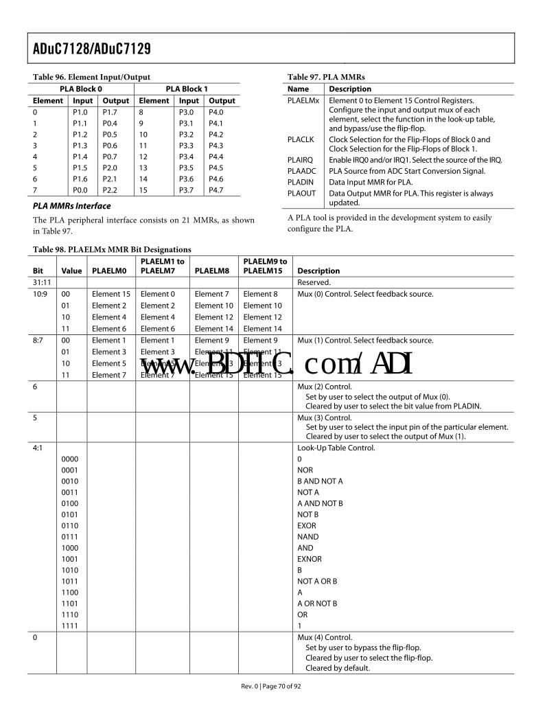
ADuC7128/ADuC7129
Rev. 0 | Page 70 of 92
Table 96. Element Input/Output PLA Block 0 PLA Block 1
Element Input Output Element Input Output 0 P1.0 P1.7 8 P3.0 P4.0 1 P1.1 P0.4 9 P3.1 P4.1 2 P1.2 P0.5 10 P3.2 P4.2 3 P1.3 P0.6 11 P3.3 P4.3 4 P1.4 P0.7 12 P3.4 P4.4 5 P1.5 P2.0 13 P3.5 P4.5 6 P1.6 P2.1 14 P3.6 P4.6 7 P0.0 P2.2 15 P3.7 P4.7
PLA MMRs Interface
The PLA peripheral interface consists on 21 MMRs, as shown in Table 97.
Table 97. PLA MMRs Name Description PLAELMx Element 0 to Element 15 Control Registers.
Configure the input and output mux of each element, select the function in the look-up table, and bypass/use the flip-flop.
PLACLK Clock Selection for the Flip-Flops of Block 0 and Clock Selection for the Flip-Flops of Block 1.
PLAIRQ Enable IRQ0 and/or IRQ1. Select the source of the IRQ. PLAADC PLA Source from ADC Start Conversion Signal. PLADIN Data Input MMR for PLA. PLAOUT Data Output MMR for PLA. This register is always
updated.
A PLA tool is provided in the development system to easily configure the PLA.
Table 98. PLAELMx MMR Bit Designations
Bit Value PLAELM0 PLAELM1 to PLAELM7 PLAELM8
PLAELM9 to PLAELM15 Description
31:11 Reserved. 00 Element 15 Element 0 Element 7 Element 8 Mux (0) Control. Select feedback source. 01 Element 2 Element 2 Element 10 Element 10 10 Element 4 Element 4 Element 12 Element 12
10:9
11 Element 6 Element 6 Element 14 Element 14 00 Element 1 Element 1 Element 9 Element 9 Mux (1) Control. Select feedback source. 01 Element 3 Element 3 Element 11 Element 11 10 Element 5 Element 5 Element 13 Element 13
8:7
11 Element 7 Element 7 Element 15 Element 15 6 Mux (2) Control.
Set by user to select the output of Mux (0). Cleared by user to select the bit value from PLADIN.
5 Mux (3) Control. Set by user to select the input pin of the particular element.Cleared by user to select the output of Mux (1).
4:1 Look-Up Table Control. 0000 0 0001 NOR 0010 B AND NOT A 0011 NOT A 0100 A AND NOT B 0101 NOT B 0110 EXOR 0111 NAND 1000 AND 1001 EXNOR 1010 B 1011 NOT A OR B 1100 A 1101 A OR NOT B 1110 OR 1111 1 0 Mux (4) Control.
Set by user to bypass the flip-flop. Cleared by user to select the flip-flop. Cleared by default.
www.BDTIC.com/ADI
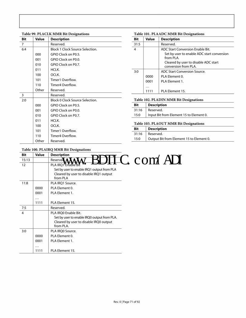
Rev. 0 | Page 71 of 92
Table 99. PLACLK MMR Bit Designations Bit Value Description 7 Reserved.
Block 1 Clock Source Selection. 000 GPIO Clock on P0.5. 001 GPIO Clock on P0.0. 010 GPIO Clock on P0.7. 011 HCLK. 100 OCLK. 101 Timer1 Overflow. 110 Timer4 Overflow.
6:4
Other Reserved. 3 Reserved.
Block 0 Clock Source Selection. 000 GPIO Clock on P0.5. 001 GPIO Clock on P0.0. 010 GPIO Clock on P0.7. 011 HCLK. 100 OCLK. 101 Timer1 Overflow. 110 Timer4 Overflow.
2:0
Other Reserved.
Table 100. PLAIRQ MMR Bit Designations Bit Value Description 15:13 Reserved. 12 PLA IRQ1 Enable Bit
Set by user to enable IRQ1 output from PLA Cleared by user to disable IRQ1 output from PLA
11:8 PLA IRQ1 Source. 0000 PLA Element 0. 0001 PLA Element 1. … 1111 PLA Element 15. 7:5 Reserved. 4 PLA IRQ0 Enable Bit.
Set by user to enable IRQ0 output from PLA. Cleared by user to disable IRQ0 output from PLA.
3:0 PLA IRQ0 Source. 0000 PLA Element 0. 0001 PLA Element 1. … 1111 PLA Element 15.
Table 101. PLAADC MMR Bit Designations Bit Value Description 31:5 Reserved. 4 ADC Start Conversion Enable Bit.
Set by user to enable ADC start conversion from PLA. Cleared by user to disable ADC start conversion from PLA.
3:0 ADC Start Conversion Source. 0000 PLA Element 0. 0001 PLA Element 1. … 1111 PLA Element 15.
Table 102. PLADIN MMR Bit Designations Bit Description 31:16 Reserved. 15:0 Input Bit from Element 15 to Element 0.
Table 103. PLAOUT MMR Bit Designations Bit Description 31:16 Reserved. 15:0 Output Bit from Element 15 to Element 0.
www.BDTIC.com/ADI
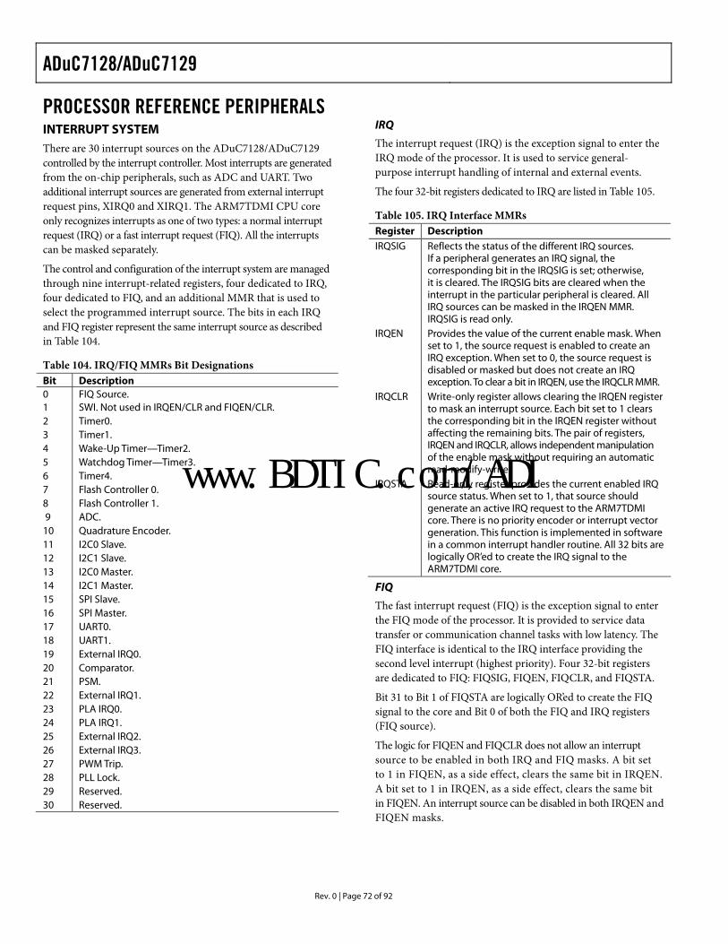
ADuC7128/ADuC7129
Rev. 0 | Page 72 of 92
PROCESSOR REFERENCE PERIPHERALSINTERRUPT SYSTEM There are 30 interrupt sources on the ADuC7128/ADuC7129 controlled by the interrupt controller. Most interrupts are generated from the on-chip peripherals, such as ADC and UART. Two additional interrupt sources are generated from external interrupt request pins, XIRQ0 and XIRQ1. The ARM7TDMI CPU core only recognizes interrupts as one of two types: a normal interrupt request (IRQ) or a fast interrupt request (FIQ). All the interrupts can be masked separately.
The control and configuration of the interrupt system are managed through nine interrupt-related registers, four dedicated to IRQ, four dedicated to FIQ, and an additional MMR that is used to select the programmed interrupt source. The bits in each IRQ and FIQ register represent the same interrupt source as described in Table 104.
Table 104. IRQ/FIQ MMRs Bit Designations Bit Description 0 FIQ Source. 1 SWI. Not used in IRQEN/CLR and FIQEN/CLR. 2 Timer0. 3 Timer1. 4 Wake-Up Timer—Timer2. 5 Watchdog Timer—Timer3. 6 Timer4. 7 Flash Controller 0. 8 Flash Controller 1. 9 ADC. 10 Quadrature Encoder. 11 I2C0 Slave. 12 I2C1 Slave. 13 I2C0 Master. 14 I2C1 Master. 15 SPI Slave. 16 SPI Master. 17 UART0. 18 UART1. 19 External IRQ0. 20 Comparator. 21 PSM. 22 External IRQ1. 23 PLA IRQ0. 24 PLA IRQ1. 25 External IRQ2. 26 External IRQ3. 27 PWM Trip. 28 PLL Lock. 29 Reserved. 30 Reserved.
IRQ
The interrupt request (IRQ) is the exception signal to enter the IRQ mode of the processor. It is used to service general-purpose interrupt handling of internal and external events.
The four 32-bit registers dedicated to IRQ are listed in Table 105.
Table 105. IRQ Interface MMRs Register Description IRQSIG Reflects the status of the different IRQ sources.
If a peripheral generates an IRQ signal, the corresponding bit in the IRQSIG is set; otherwise, it is cleared. The IRQSIG bits are cleared when the interrupt in the particular peripheral is cleared. All IRQ sources can be masked in the IRQEN MMR. IRQSIG is read only.
IRQEN Provides the value of the current enable mask. When set to 1, the source request is enabled to create an IRQ exception. When set to 0, the source request is disabled or masked but does not create an IRQ exception. To clear a bit in IRQEN, use the IRQCLR MMR.
IRQCLR Write-only register allows clearing the IRQEN register to mask an interrupt source. Each bit set to 1 clears the corresponding bit in the IRQEN register without affecting the remaining bits. The pair of registers, IRQEN and IRQCLR, allows independent manipulation of the enable mask without requiring an automatic read-modify-write.
IRQSTA Read-only register provides the current enabled IRQ source status. When set to 1, that source should generate an active IRQ request to the ARM7TDMI core. There is no priority encoder or interrupt vector generation. This function is implemented in software in a common interrupt handler routine. All 32 bits are logically OR’ed to create the IRQ signal to the ARM7TDMI core.
FIQ
The fast interrupt request (FIQ) is the exception signal to enter the FIQ mode of the processor. It is provided to service data transfer or communication channel tasks with low latency. The FIQ interface is identical to the IRQ interface providing the second level interrupt (highest priority). Four 32-bit registers are dedicated to FIQ: FIQSIG, FIQEN, FIQCLR, and FIQSTA.
Bit 31 to Bit 1 of FIQSTA are logically OR’ed to create the FIQ signal to the core and Bit 0 of both the FIQ and IRQ registers (FIQ source).
The logic for FIQEN and FIQCLR does not allow an interrupt source to be enabled in both IRQ and FIQ masks. A bit set to 1 in FIQEN, as a side effect, clears the same bit in IRQEN. A bit set to 1 in IRQEN, as a side effect, clears the same bit in FIQEN. An interrupt source can be disabled in both IRQEN and FIQEN masks.
www.BDTIC.com/ADI
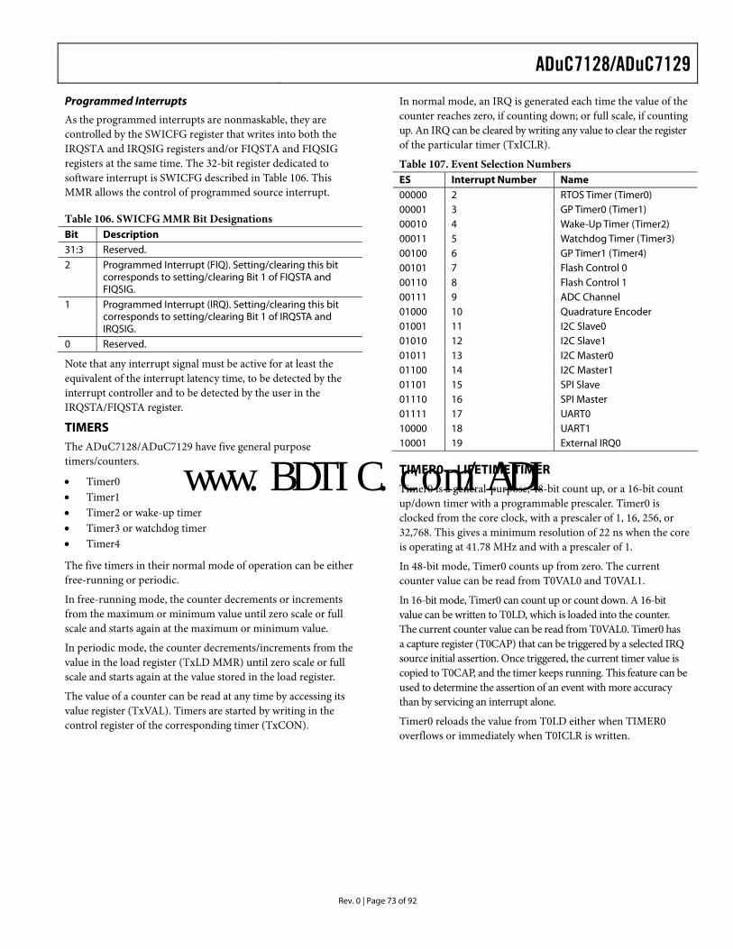
ADuC7128/ADuC7129
Rev. 0 | Page 73 of 92
Programmed Interrupts
As the programmed interrupts are nonmaskable, they are controlled by the SWICFG register that writes into both the IRQSTA and IRQSIG registers and/or FIQSTA and FIQSIG registers at the same time. The 32-bit register dedicated to software interrupt is SWICFG described in Table 106. This MMR allows the control of programmed source interrupt.
Table 106. SWICFG MMR Bit Designations Bit Description 31:3 Reserved. 2 Programmed Interrupt (FIQ). Setting/clearing this bit
corresponds to setting/clearing Bit 1 of FIQSTA and FIQSIG.
1 Programmed Interrupt (IRQ). Setting/clearing this bit corresponds to setting/clearing Bit 1 of IRQSTA and IRQSIG.
0 Reserved.
Note that any interrupt signal must be active for at least the equivalent of the interrupt latency time, to be detected by the interrupt controller and to be detected by the user in the IRQSTA/FIQSTA register.
TIMERS The ADuC7128/ADuC7129 have five general purpose timers/counters.
• Timer0 • Timer1 • Timer2 or wake-up timer • Timer3 or watchdog timer • Timer4
The five timers in their normal mode of operation can be either free-running or periodic.
In free-running mode, the counter decrements or increments from the maximum or minimum value until zero scale or full scale and starts again at the maximum or minimum value.
In periodic mode, the counter decrements/increments from the value in the load register (TxLD MMR) until zero scale or full scale and starts again at the value stored in the load register.
The value of a counter can be read at any time by accessing its value register (TxVAL). Timers are started by writing in the control register of the corresponding timer (TxCON).
In normal mode, an IRQ is generated each time the value of the counter reaches zero, if counting down; or full scale, if counting up. An IRQ can be cleared by writing any value to clear the register of the particular timer (TxICLR).
Table 107. Event Selection Numbers ES Interrupt Number Name 00000 2 RTOS Timer (Timer0) 00001 3 GP Timer0 (Timer1) 00010 4 Wake-Up Timer (Timer2) 00011 5 Watchdog Timer (Timer3) 00100 6 GP Timer1 (Timer4) 00101 7 Flash Control 0 00110 8 Flash Control 1 00111 9 ADC Channel 01000 10 Quadrature Encoder 01001 11 I2C Slave0 01010 12 I2C Slave1 01011 13 I2C Master0 01100 14 I2C Master1 01101 15 SPI Slave 01110 16 SPI Master 01111 17 UART0 10000 18 UART1 10001 19 External IRQ0
TIMER0—LIFETIME TIMER Timer0 is a general-purpose, 48-bit count up, or a 16-bit count up/down timer with a programmable prescaler. Timer0 is clocked from the core clock, with a prescaler of 1, 16, 256, or 32,768. This gives a minimum resolution of 22 ns when the core is operating at 41.78 MHz and with a prescaler of 1.
In 48-bit mode, Timer0 counts up from zero. The current counter value can be read from T0VAL0 and T0VAL1.
In 16-bit mode, Timer0 can count up or count down. A 16-bit value can be written to T0LD, which is loaded into the counter. The current counter value can be read from T0VAL0. Timer0 has a capture register (T0CAP) that can be triggered by a selected IRQ source initial assertion. Once triggered, the current timer value is copied to T0CAP, and the timer keeps running. This feature can be used to determine the assertion of an event with more accuracy than by servicing an interrupt alone.
Timer0 reloads the value from T0LD either when TIMER0 overflows or immediately when T0ICLR is written.
www.BDTIC.com/ADI
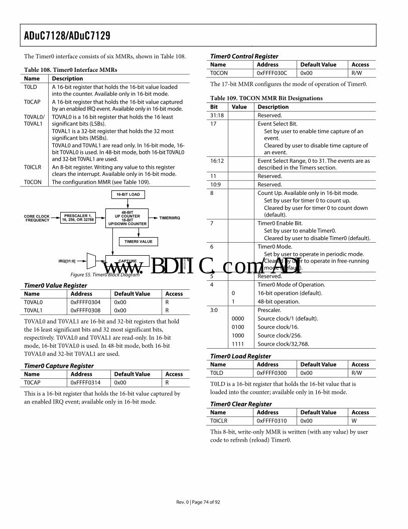
ADuC7128/ADuC7129
Rev. 0 | Page 74 of 92
The Timer0 interface consists of six MMRs, shown in Table 108.
Table 108. Timer0 Interface MMRs Name Description T0LD A 16-bit register that holds the 16-bit value loaded
into the counter. Available only in 16-bit mode. T0CAP A 16-bit register that holds the 16-bit value captured
by an enabled IRQ event. Available only in 16-bit mode. T0VAL0/ T0VAL1
TOVAL0 is a 16 bit register that holds the 16 least significant bits (LSBs). T0VAL1 is a 32-bit register that holds the 32 most significant bits (MSBs). T0VAL0 and T0VAL1 are read only. In 16-bit mode, 16-bit T0VAL0 is used. In 48-bit mode, both 16-bit T0VAL0 and 32-bit T0VAL1 are used.
T0ICLR An 8-bit register. Writing any value to this register clears the interrupt. Available only in 16-bit mode.
T0CON The configuration MMR (see Table 109).
TIMER0IRQCORE CLOCKFREQUENCY
CAPTUREIRQ[31:0]
16-BIT LOAD
48-BITUP COUNTER
16-BITUP/DOWN COUNTER
TIMER0 VALUE
PRESCALER 1,16, 256, OR 32768
0602
0-05
0
Figure 55. Timer0 Block Diagram
Timer0 Value Register Name Address Default Value Access T0VAL0 0xFFFF0304 0x00 R T0VAL1 0xFFFF0308 0x00 R
T0VAL0 and T0VAL1 are 16-bit and 32-bit registers that hold the 16 least significant bits and 32 most significant bits, respectively. T0VAL0 and T0VAL1 are read-only. In 16-bit mode, 16-bit T0VAL0 is used. In 48-bit mode, both 16-bit T0VAL0 and 32-bit T0VAL1 are used.
Timer0 Capture Register Name Address Default Value Access T0CAP 0xFFFF0314 0x00 R
This is a 16-bit register that holds the 16-bit value captured by an enabled IRQ event; available only in 16-bit mode.
Timer0 Control Register Name Address Default Value Access T0CON 0xFFFF030C 0x00 R/W
The 17-bit MMR configures the mode of operation of Timer0.
Table 109. T0CON MMR Bit Designations Bit Value Description 31:18 Reserved. 17 Event Select Bit.
Set by user to enable time capture of an event. Cleared by user to disable time capture of an event.
16:12 Event Select Range, 0 to 31. The events are as described in the Timers section.
11 Reserved. 10:9 Reserved. 8 Count Up. Available only in 16-bit mode.
Set by user for timer 0 to count up. Cleared by user for timer 0 to count down (default).
7 Timer0 Enable Bit. Set by user to enable Timer0. Cleared by user to disable Timer0 (default).
6 Timer0 Mode. Set by user to operate in periodic mode. Cleared by user to operate in free-running mode (default).
5 Reserved. Timer0 Mode of Operation. 0 16-bit operation (default).
4
1 48-bit operation. Prescaler. 0000 Source clock/1 (default). 0100 Source clock/16. 1000 Source clock/256.
3:0
1111 Source clock/32,768.
Timer0 Load Register Name Address Default Value Access T0LD 0xFFFF0300 0x00 R/W
T0LD is a 16-bit register that holds the 16-bit value that is loaded into the counter; available only in 16-bit mode.
Timer0 Clear Register Name Address Default Value Access T0ICLR 0xFFFF0310 0x00 W
This 8-bit, write-only MMR is written (with any value) by user code to refresh (reload) Timer0.
www.BDTIC.com/ADI
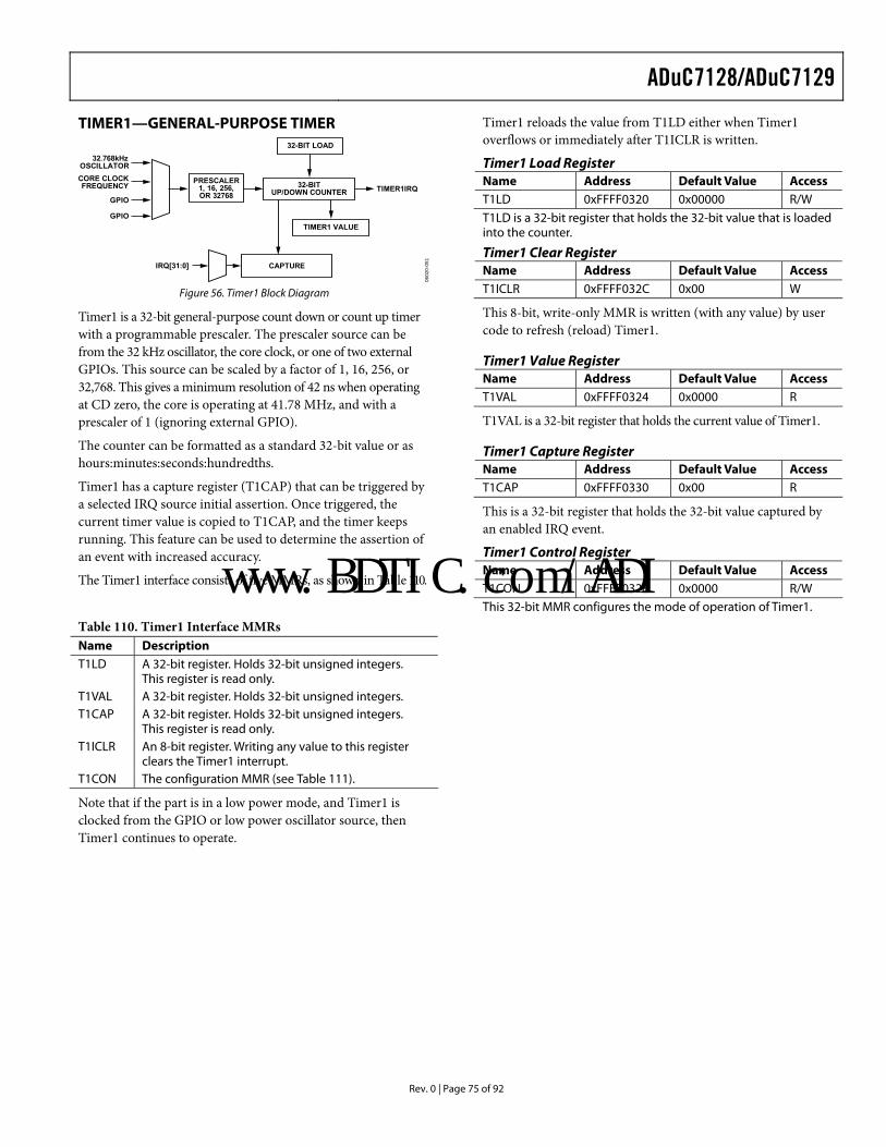
ADuC7128/ADuC7129
Rev. 0 | Page 75 of 92
TIMER1—GENERAL-PURPOSE TIMER
TIMER1IRQ
CAPTUREIRQ[31:0]
32-BIT LOAD
32-BITUP/DOWN COUNTER
TIMER1 VALUE
PRESCALER1, 16, 256,OR 32768
32.768kHzOSCILLATORCORE CLOCKFREQUENCY
GPIO
GPIO
0602
0-05
1
Figure 56. Timer1 Block Diagram
Timer1 is a 32-bit general-purpose count down or count up timer with a programmable prescaler. The prescaler source can be from the 32 kHz oscillator, the core clock, or one of two external GPIOs. This source can be scaled by a factor of 1, 16, 256, or 32,768. This gives a minimum resolution of 42 ns when operating at CD zero, the core is operating at 41.78 MHz, and with a prescaler of 1 (ignoring external GPIO).
The counter can be formatted as a standard 32-bit value or as hours:minutes:seconds:hundredths.
Timer1 has a capture register (T1CAP) that can be triggered by a selected IRQ source initial assertion. Once triggered, the current timer value is copied to T1CAP, and the timer keeps running. This feature can be used to determine the assertion of an event with increased accuracy.
The Timer1 interface consists of five MMRs, as shown in Table 110.
Table 110. Timer1 Interface MMRs Name Description T1LD A 32-bit register. Holds 32-bit unsigned integers.
This register is read only. T1VAL A 32-bit register. Holds 32-bit unsigned integers. T1CAP A 32-bit register. Holds 32-bit unsigned integers.
This register is read only. T1ICLR An 8-bit register. Writing any value to this register
clears the Timer1 interrupt. T1CON The configuration MMR (see Table 111).
Note that if the part is in a low power mode, and Timer1 is clocked from the GPIO or low power oscillator source, then Timer1 continues to operate.
Timer1 reloads the value from T1LD either when Timer1 overflows or immediately after T1ICLR is written.
Timer1 Load Register Name Address Default Value Access T1LD 0xFFFF0320 0x00000 R/W
T1LD is a 32-bit register that holds the 32-bit value that is loaded into the counter.
Timer1 Clear Register Name Address Default Value Access T1ICLR 0xFFFF032C 0x00 W
This 8-bit, write-only MMR is written (with any value) by user code to refresh (reload) Timer1.
Timer1 Value Register Name Address Default Value Access T1VAL 0xFFFF0324 0x0000 R
T1VAL is a 32-bit register that holds the current value of Timer1.
Timer1 Capture Register Name Address Default Value Access T1CAP 0xFFFF0330 0x00 R
This is a 32-bit register that holds the 32-bit value captured by an enabled IRQ event.
Timer1 Control Register Name Address Default Value Access T1CON 0xFFFF0328 0x0000 R/W This 32-bit MMR configures the mode of operation of Timer1.
www.BDTIC.com/ADI
ADuC7128/ADuC7129
Rev. 0 | Page 76 of 92
Table 111. T1CON MMR Bit Designations Bit Value Description 31:18 Reserved. Should be set to 0 by the user. 17 Event Select Bit.
Set by user to enable time capture of an event. Cleared by user to disable time capture of an event.
16:12 Event Select Range, 0 to 31. The events are as described in the introduction to the timers. Clock Select. 000 Core Clock (Default). 001 32.768 kHz Oscillator. 010 P1.0.
11:9
011 P0.6. 8 Count Up.
Set by user for Timer1 to count up. Cleared by user for Timer1 to count down (default).
7 Timer1 Enable Bit. Set by user to enable Timer1. Cleared by user to disable Timer1 (default).
6 Timer1 Mode. Set by user to operate in periodic mode. Cleared by user to operate in free-running mode (default).
Format. 00 Binary (Default). 01 Reserved. 10 Hours:Minutes:Seconds:Hundredths: 23 Hours to 0 Hours.
5:4
11 Hours:Minutes:Seconds:Hundredths: 255 Hours to 0 Hours. Prescaler. 0000 Source Clock/1 (Default). 0100 Source Clock/16. 1000 Source Clock/256.
3:0
1111 Source Clock/32768.
www.BDTIC.com/ADI
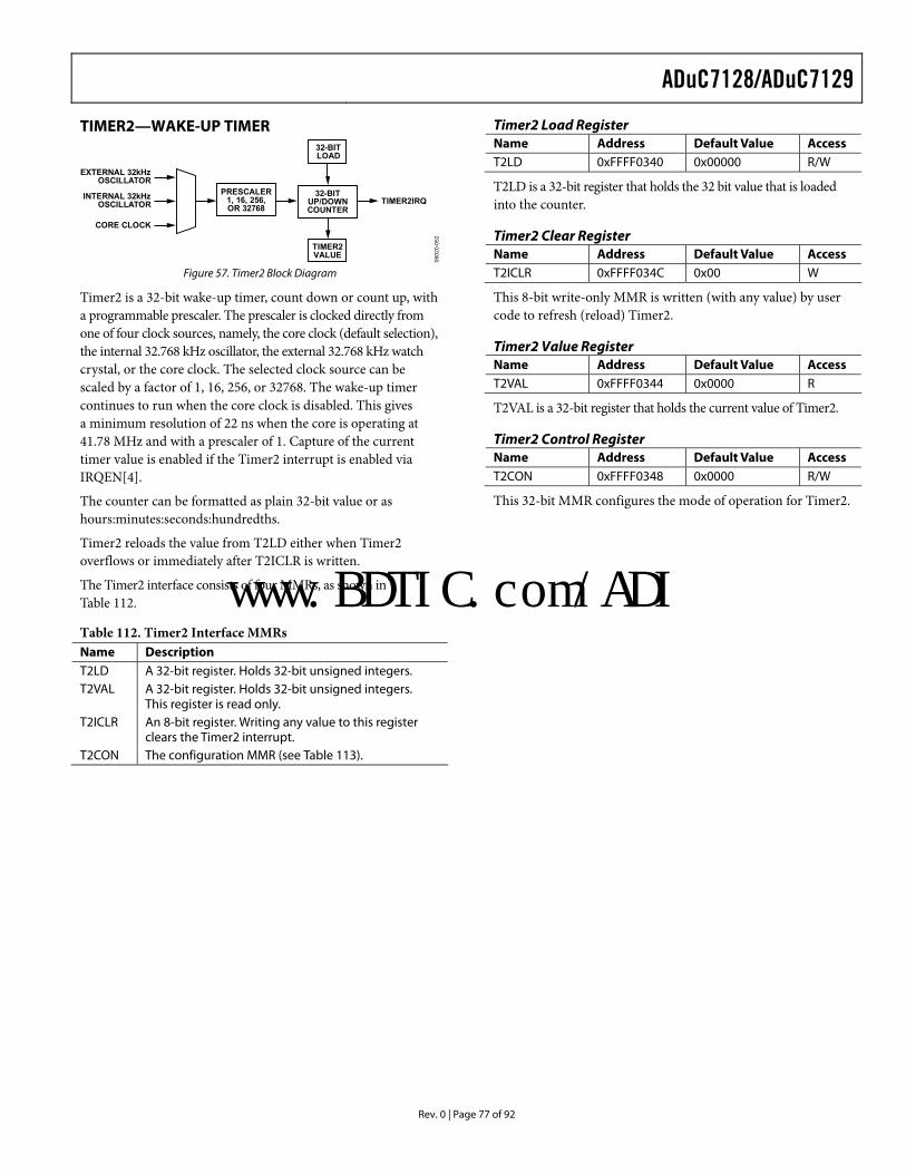
ADuC7128/ADuC7129
Rev. 0 | Page 77 of 92
TIMER2—WAKE-UP TIMER
TIMER2IRQ
32-BITLOAD
32-BITUP/DOWNCOUNTER
TIMER2VALUE
PRESCALER1, 16, 256,OR 32768
EXTERNAL 32kHzOSCILLATOR
INTERNAL 32kHzOSCILLATOR
CORE CLOCK
0602
0-05
2
Figure 57. Timer2 Block Diagram
Timer2 is a 32-bit wake-up timer, count down or count up, with a programmable prescaler. The prescaler is clocked directly from one of four clock sources, namely, the core clock (default selection), the internal 32.768 kHz oscillator, the external 32.768 kHz watch crystal, or the core clock. The selected clock source can be scaled by a factor of 1, 16, 256, or 32768. The wake-up timer continues to run when the core clock is disabled. This gives a minimum resolution of 22 ns when the core is operating at 41.78 MHz and with a prescaler of 1. Capture of the current timer value is enabled if the Timer2 interrupt is enabled via IRQEN[4].
The counter can be formatted as plain 32-bit value or as hours:minutes:seconds:hundredths.
Timer2 reloads the value from T2LD either when Timer2 overflows or immediately after T2ICLR is written.
The Timer2 interface consists of four MMRs, as shown in Table 112.
Table 112. Timer2 Interface MMRs Name Description T2LD A 32-bit register. Holds 32-bit unsigned integers. T2VAL A 32-bit register. Holds 32-bit unsigned integers.
This register is read only. T2ICLR An 8-bit register. Writing any value to this register
clears the Timer2 interrupt. T2CON The configuration MMR (see Table 113).
Timer2 Load Register Name Address Default Value Access T2LD 0xFFFF0340 0x00000 R/W
T2LD is a 32-bit register that holds the 32 bit value that is loaded into the counter.
Timer2 Clear Register Name Address Default Value Access T2ICLR 0xFFFF034C 0x00 W
This 8-bit write-only MMR is written (with any value) by user code to refresh (reload) Timer2.
Timer2 Value Register Name Address Default Value Access T2VAL 0xFFFF0344 0x0000 R
T2VAL is a 32-bit register that holds the current value of Timer2.
Timer2 Control Register Name Address Default Value Access T2CON 0xFFFF0348 0x0000 R/W
This 32-bit MMR configures the mode of operation for Timer2.
www.BDTIC.com/ADI
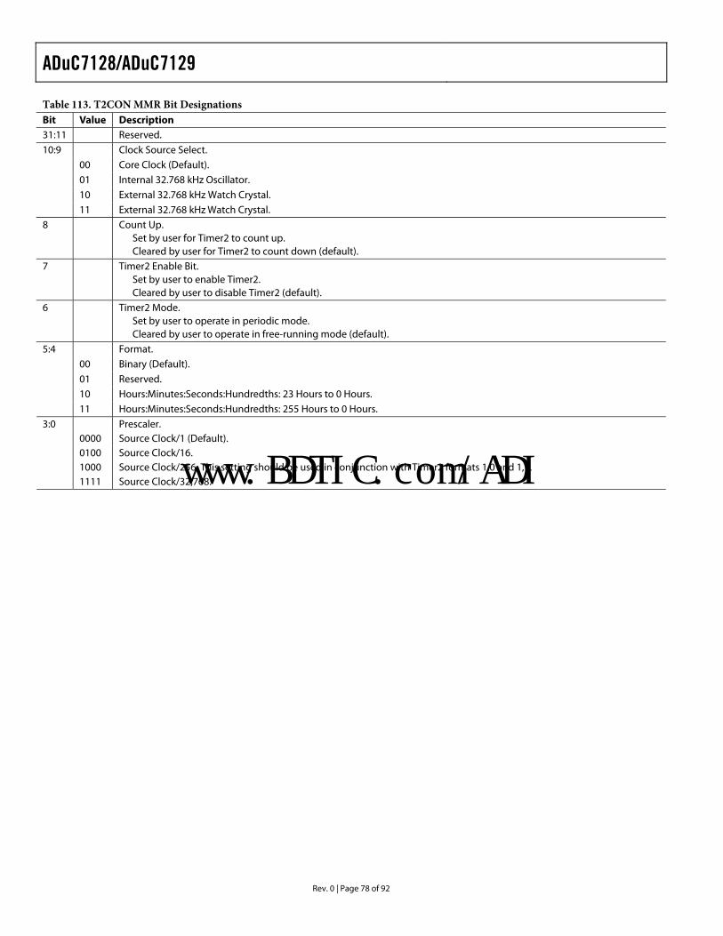
ADuC7128/ADuC7129
Rev. 0 | Page 78 of 92
Table 113. T2CON MMR Bit Designations Bit Value Description 31:11 Reserved.
Clock Source Select. 00 Core Clock (Default). 01 Internal 32.768 kHz Oscillator. 10 External 32.768 kHz Watch Crystal.
10:9
11 External 32.768 kHz Watch Crystal. 8 Count Up.
Set by user for Timer2 to count up. Cleared by user for Timer2 to count down (default).
7 Timer2 Enable Bit. Set by user to enable Timer2. Cleared by user to disable Timer2 (default).
6 Timer2 Mode. Set by user to operate in periodic mode. Cleared by user to operate in free-running mode (default).
Format. 00 Binary (Default). 01 Reserved. 10 Hours:Minutes:Seconds:Hundredths: 23 Hours to 0 Hours.
5:4
11 Hours:Minutes:Seconds:Hundredths: 255 Hours to 0 Hours. Prescaler. 0000 Source Clock/1 (Default). 0100 Source Clock/16. 1000 Source Clock/256. This setting should be used in conjunction with Timer2 formats 1,0 and 1,1.
3:0
1111 Source Clock/32,768.
www.BDTIC.com/ADI
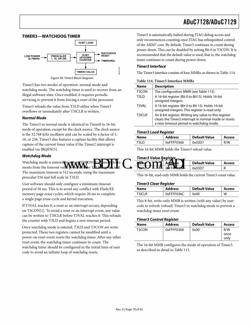
ADuC7128/ADuC7129
Rev. 0 | Page 79 of 92
TIMER3—WATCHDOG TIMER
TIMER3IRQ
16-BIT LOAD
16-BITUP/DOWNCOUNTER
TIMER3 VALUE
PRESCALER1, 16, OR 256
WATCHDOGRESETLOW POWER
32.768kHz
0602
0-05
3
Figure 58. Timer3 Block Diagram
Timer3 has two modes of operation: normal mode and watchdog mode. The watchdog timer is used to recover from an illegal software state. Once enabled, it requires periodic servicing to prevent it from forcing a reset of the processor.
Timer3 reloads the value from T3LD either when Timer3 overflows or immediately after T3ICLR is written.
Normal Mode
The Timer3 in normal mode is identical to Timer0 in 16-bit mode of operation, except for the clock source. The clock source is the 32.768 kHz oscillator and can be scaled by a factor of 1, 16, or 256. Timer3 also features a capture facility that allows capture of the current timer value if the Timer2 interrupt is enabled via IRQEN[5].
Watchdog Mode
Watchdog mode is entered by setting T3CON[5]. Timer3 decre-ments from the timeout value present in the T3LD register to 0. The maximum timeout is 512 seconds, using the maximum prescalar/256 and full scale in T3LD.
User software should only configure a minimum timeout period of 30 ms. This is to avoid any conflict with Flash/EE memory page erase cycles, which require 20 ms to complete a single page erase cycle and kernel execution.
If T3VAL reaches 0, a reset or an interrupt occurs, depending on T3CON[1]. To avoid a reset or an interrupt event, any value can be written to T3ICLR before T3VAL reaches 0. This reloads the counter with T3LD and begins a new timeout period.
Once watchdog mode is entered, T3LD and T3CON are write protected. These two registers cannot be modified until a power-on reset event resets the watchdog timer. After any other reset event, the watchdog timer continues to count. The watchdog timer should be configured in the initial lines of user code to avoid an infinite loop of watchdog resets.
Timer3 is automatically halted during JTAG debug access and only recommences counting once JTAG has relinquished control of the ARM7 core. By default, Timer3 continues to count during power-down. This can be disabled by setting Bit 0 in T3CON. It is recommended that the default value is used, that is, the watchdog timer continues to count during power-down.
Timer3 Interface
The Timer3 interface consists of four MMRs, as shown in Table 114.
Table 114. Timer3 Interface MMRs Name Description T3CON The configuration MMR (see Table 115). T3LD A 16-bit register (Bit 0 to Bit15). Holds 16-bit
unsigned integers. T3VAL A 16-bit register (Bit 0 to Bit 15). Holds 16-bit
unsigned integers. This register is read only. T3ICLR An 8-bit register. Writing any value to this register
clears the Timer3 interrupt in normal mode or resets a new timeout period in watchdog mode.
Timer3 Load Register Name Address Default Value Access T3LD 0xFFFF0360 0x03D7 R/W
This 16-bit MMR holds the Timer3 reload value.
Timer3 Value Register Name Address Default Value Access T3VAL 0xFFFF0364 0x03D7 R
This 16-bit, read-only MMR holds the current Timer3 count value.
Timer3 Clear Register Name Address Default Value Access T3ICLR 0xFFFF036C 0x00 W
This 8-bit, write-only MMR is written (with any value) by user code to refresh (reload) Timer3 in watchdog mode to prevent a watchdog timer reset event.
Timer3 Control Register Name Address Default Value Access T3CON 0xFFFF0368 0x00 R/W
once only
The 16-bit MMR configures the mode of operation of Timer3. as described in detail in Table 115.
www.BDTIC.com/ADI
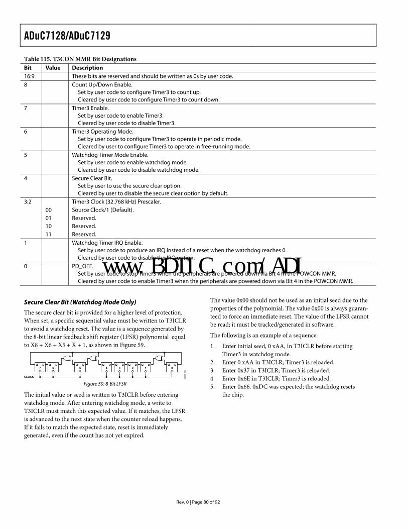
ADuC7128/ADuC7129
Rev. 0 | Page 80 of 92
Table 115. T3CON MMR Bit Designations Bit Value Description 16:9 These bits are reserved and should be written as 0s by user code. 8 Count Up/Down Enable.
Set by user code to configure Timer3 to count up. Cleared by user code to configure Timer3 to count down.
7 Timer3 Enable. Set by user code to enable Timer3. Cleared by user code to disable Timer3.
6 Timer3 Operating Mode. Set by user code to configure Timer3 to operate in periodic mode. Cleared by user to configure Timer3 to operate in free-running mode.
5 Watchdog Timer Mode Enable. Set by user code to enable watchdog mode. Cleared by user code to disable watchdog mode.
4 Secure Clear Bit. Set by user to use the secure clear option. Cleared by user to disable the secure clear option by default.
3:2 Timer3 Clock (32.768 kHz) Prescaler. 00 Source Clock/1 (Default). 01 Reserved. 10 Reserved. 11 Reserved. 1 Watchdog Timer IRQ Enable.
Set by user code to produce an IRQ instead of a reset when the watchdog reaches 0. Cleared by user code to disable the IRQ option.
0 PD_OFF. Set by user code to stop Timer3 when the peripherals are powered down via Bit 4 in the POWCON MMR. Cleared by user code to enable Timer3 when the peripherals are powered down via Bit 4 in the POWCON MMR.
Secure Clear Bit (Watchdog Mode Only)
The secure clear bit is provided for a higher level of protection. When set, a specific sequential value must be written to T3ICLR to avoid a watchdog reset. The value is a sequence generated by the 8-bit linear feedback shift register (LFSR) polynomial equal to X8 + X6 + X5 + X + 1, as shown in Figure 59.
CLOCK
Q D4
Q D5
Q D3
Q D7
Q D6
Q D2
Q D1
Q D0
0602
0-05
4
Figure 59. 8-Bit LFSR
The initial value or seed is written to T3ICLR before entering watchdog mode. After entering watchdog mode, a write to T3ICLR must match this expected value. If it matches, the LFSR is advanced to the next state when the counter reload happens. If it fails to match the expected state, reset is immediately generated, even if the count has not yet expired.
The value 0x00 should not be used as an initial seed due to the properties of the polynomial. The value 0x00 is always guaran-teed to force an immediate reset. The value of the LFSR cannot be read; it must be tracked/generated in software.
The following is an example of a sequence:
1. Enter initial seed, 0 xAA, in T3ICLR before starting Timer3 in watchdog mode.
2. Enter 0 xAA in T3ICLR; Timer3 is reloaded. 3. Enter 0x37 in T3ICLR; Timer3 is reloaded. 4. Enter 0x6E in T3ICLR; Timer3 is reloaded. 5. Enter 0x66. 0xDC was expected; the watchdog resets
the chip.
www.BDTIC.com/ADI
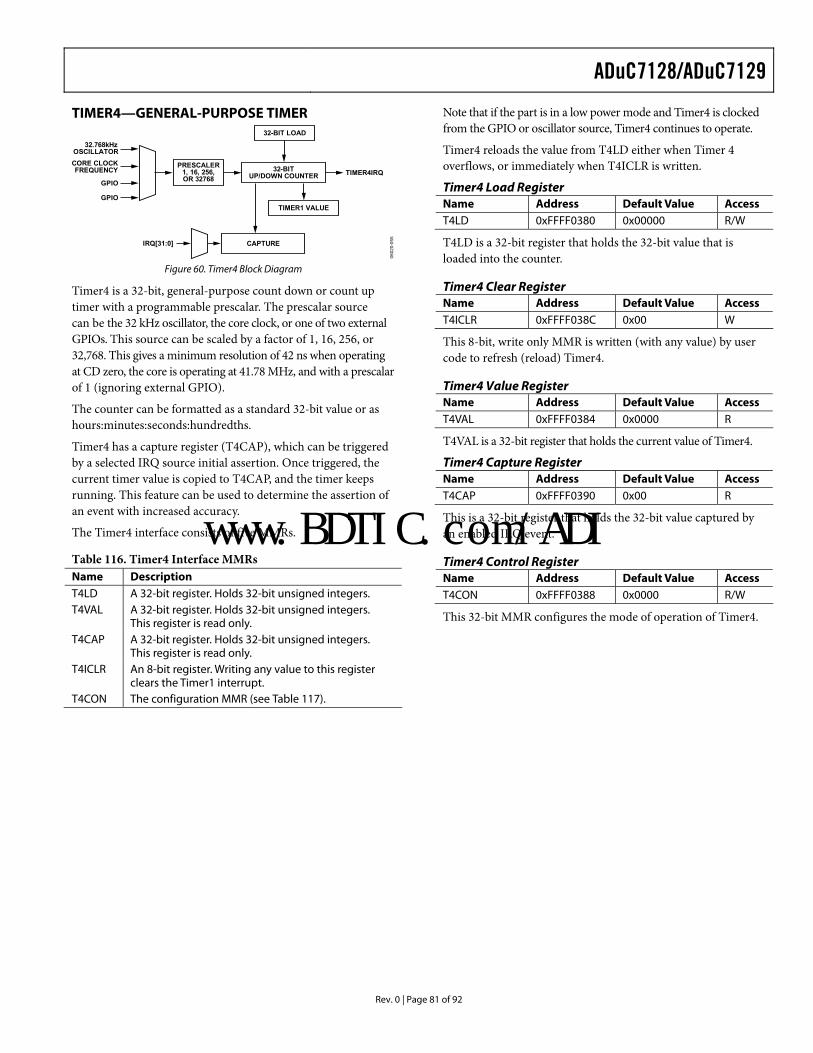
ADuC7128/ADuC7129
Rev. 0 | Page 81 of 92
TIMER4—GENERAL-PURPOSE TIMER
TIMER4IRQ
CAPTUREIRQ[31:0]
32-BIT LOAD
32-BITUP/DOWN COUNTER
TIMER1 VALUE
PRESCALER1, 16, 256,OR 32768
32.768kHzOSCILLATORCORE CLOCKFREQUENCY
GPIO
GPIO
0602
0-05
5
Figure 60. Timer4 Block Diagram
Timer4 is a 32-bit, general-purpose count down or count up timer with a programmable prescalar. The prescalar source can be the 32 kHz oscillator, the core clock, or one of two external GPIOs. This source can be scaled by a factor of 1, 16, 256, or 32,768. This gives a minimum resolution of 42 ns when operating at CD zero, the core is operating at 41.78 MHz, and with a prescalar of 1 (ignoring external GPIO).
The counter can be formatted as a standard 32-bit value or as hours:minutes:seconds:hundredths.
Timer4 has a capture register (T4CAP), which can be triggered by a selected IRQ source initial assertion. Once triggered, the current timer value is copied to T4CAP, and the timer keeps running. This feature can be used to determine the assertion of an event with increased accuracy.
The Timer4 interface consists of five MMRs.
Table 116. Timer4 Interface MMRs Name Description T4LD A 32-bit register. Holds 32-bit unsigned integers. T4VAL A 32-bit register. Holds 32-bit unsigned integers.
This register is read only. T4CAP A 32-bit register. Holds 32-bit unsigned integers.
This register is read only. T4ICLR An 8-bit register. Writing any value to this register
clears the Timer1 interrupt. T4CON The configuration MMR (see Table 117).
Note that if the part is in a low power mode and Timer4 is clocked from the GPIO or oscillator source, Timer4 continues to operate.
Timer4 reloads the value from T4LD either when Timer 4 overflows, or immediately when T4ICLR is written.
Timer4 Load Register Name Address Default Value Access T4LD 0xFFFF0380 0x00000 R/W
T4LD is a 32-bit register that holds the 32-bit value that is loaded into the counter.
Timer4 Clear Register Name Address Default Value Access T4ICLR 0xFFFF038C 0x00 W
This 8-bit, write only MMR is written (with any value) by user code to refresh (reload) Timer4.
Timer4 Value Register Name Address Default Value Access T4VAL 0xFFFF0384 0x0000 R
T4VAL is a 32-bit register that holds the current value of Timer4.
Timer4 Capture Register Name Address Default Value Access T4CAP 0xFFFF0390 0x00 R
This is a 32-bit register that holds the 32-bit value captured by an enabled IRQ event.
Timer4 Control Register Name Address Default Value Access T4CON 0xFFFF0388 0x0000 R/W
This 32-bit MMR configures the mode of operation of Timer4.
www.BDTIC.com/ADI
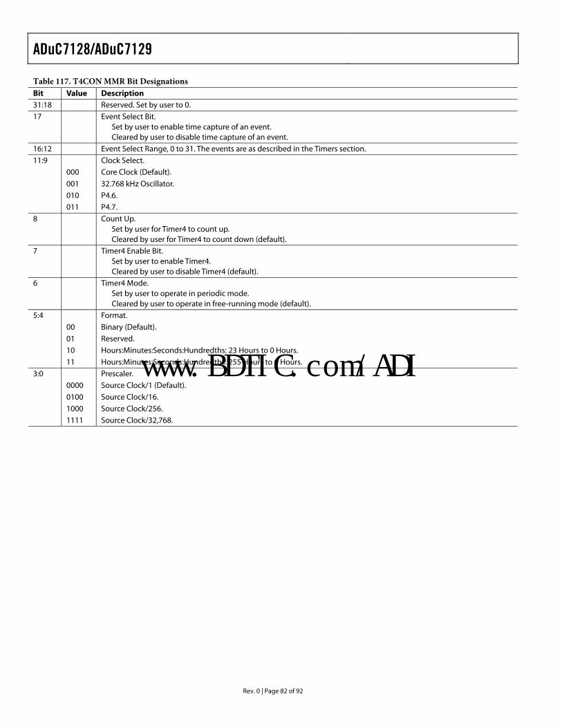
ADuC7128/ADuC7129
Rev. 0 | Page 82 of 92
Table 117. T4CON MMR Bit Designations Bit Value Description 31:18 Reserved. Set by user to 0. 17 Event Select Bit.
Set by user to enable time capture of an event. Cleared by user to disable time capture of an event.
16:12 Event Select Range, 0 to 31. The events are as described in the Timers section. Clock Select. 000 Core Clock (Default). 001 32.768 kHz Oscillator. 010 P4.6.
11:9
011 P4.7. 8 Count Up.
Set by user for Timer4 to count up. Cleared by user for Timer4 to count down (default).
7 Timer4 Enable Bit. Set by user to enable Timer4. Cleared by user to disable Timer4 (default).
6 Timer4 Mode. Set by user to operate in periodic mode. Cleared by user to operate in free-running mode (default).
Format. 00 Binary (Default). 01 Reserved. 10 Hours:Minutes:Seconds:Hundredths: 23 Hours to 0 Hours.
5:4
11 Hours:Minutes:Seconds:Hundredths: 255 Hours to 0 Hours. Prescaler. 0000 Source Clock/1 (Default). 0100 Source Clock/16. 1000 Source Clock/256.
3:0
1111 Source Clock/32,768.
www.BDTIC.com/ADI
ADuC7128/ADuC7129
Rev. 0 | Page 83 of 92
EXTERNAL MEMORY INTERFACING The ADuC7129 is the only model in the series that features an external memory interface. The external memory interface requires a larger number of pins. This is why it is only available on larger pin count packages. The XMCFG MMR must be set to 1 to use the external port.
Although 32-bit addresses are supported internally, only the lower 16 bits of the address are on external pins.
The memory interface can address up to four 128 kB regions of asynchronous memory (SRAM and/or EEPROM).
The pins required for interfacing to an external memory are shown in Table 118.
Table 118. External Memory Interfacing Pins Pin Function AD[15:0] Address/Data Bus. A16 Extended Addressing for 8-Bit Memory Only. MS[3:0] Memory Select. WR (WR) Write Strobe.
RS (RS) Read Strobe.
AE Address Latch Enable. BHE, BLE Byte Write Capability.
There are four external memory regions available, as described in Table 119. Associated with each region are the MS[3:0] pins. These signals allow access to the particular region of external memory. The size of each memory region can be 128 kB maximum, 64 k × 16, or 128 k × 8. To access 128 kB with an 8-bit memory, an extra address line (A16) is provided. (See the example in Figure 61). The four regions are configured inde-pendently.
Table 119. Memory Regions Address Start Address End Contents 0x10000000 0x1000FFFF External Memory 0 0x20000000 0x2000FFFF External Memory 1 0x30000000 0x3000FFFF External Memory 2 0x40000000 0x4000FFFF External Memory 3
Each external memory region can be controlled through three MMRs: XMCFG, XMxCON, and XMxPAR.
0602
0-06
8
LATCH
ADuC7128/ADuC7129
AD15:0A16
EPROM64k × 16-BIT
A0:15
D0 TO D15
CS
RAM128k × 8-BIT
A0:15A16
D0 TO D7
CSWEOE
WEOE
AE
MS0MS1
WSRS
Figure 61. Interfacing to External EPROM/RAM
XMCFG Register Name Address Default Value Access XMCFG 0xFFFFF000 0x00 R/W
XMCFG is set to 1 to enable external memory access. This must be set to 1 before any port pins function as external memory access pins. The port pins must also be individually enabled via the GPxCON MMR.
XMxCON Registers Name Address Default Value Access XM0CON 0xFFFFF010 0x00 R/W XM1CON 0xFFFFF014 0x00 R/W XM2CON 0xFFFFF018 0x00 R/W XM3CON 0xFFFFF01C 0x00 R/W
XMxCON registers are the control registers for each memory region. They allow the enabling/disabling of a memory region and control the data bus width of the memory region.
Table 120. XMxCON MMR Bit Designations Bit Description 1 Data Bus Width Select.
Set by the user to select a 16-bit data bus. Cleared by the user to select an 8-bit data bus.
0 Memory Region Enable. Set by the user to enable memory region. Cleared by the user to disable the memory region.
XMxPAR Registers Name Address Default Value Access XM0PAR 0xFFFFF020 0x70FF R/W XM1PAR 0xFFFFF024 0x70FF R/W XM2PAR 0xFFFFF028 0x70FF R/W XM3PAR 0xFFFFF02C 0x70FF R/W
www.BDTIC.com/ADI
ADuC7128/ADuC7129
Rev. 0 | Page 84 of 92
The XMxPAR are registers that define the protocol used for accessing the external memory for each memory region.
Table 121. XMxPAR MMR Bit Designations Bit Description 15 Enable Byte Write Strobe. This bit is only used for two,
8-bit memory sharing the same memory region. Set by user to gate the AD0 output with the WS output. This allows byte write capability without using BHE and BLE signals. Cleared by user to use BHE and BLE signals.
14:12 Number of Wait States on the Address Latch Enable Strobe. 11 Reserved. 10 Extra Address Hold Time.
Set by the user to disable extra hold time. Cleared by the user to enable one clock cycle of hold on the address in read and write.
9 Extra Bus Transition Time on Read. Set by the user to disable extra bus transition time. Cleared by the user to enable one extra clock before and after the read select (RS).
8 Extra Bus Transition Time on Write. Set by the user to disable extra bus transition time. Cleared by the user to enable one extra clock before and after the write select (WS).
7:4 Number of Write Wait States. Select the number of wait states added to the length of the WS pulse. 0x0 is 1 clock cycle; 0xF is 16 clock cycles (default value).
3:0 Number of Read Wait States. Select the number of wait states added to the length of the RS pulse. 0x0 is 1 clock cycle; 0xF is 16 clock cycles (default value).
TIMING DIAGRAMS Figure 62 through Figure 65 show the timing for a read cycle (see Figure 62), a read cycle with address hold and bus turn cycles (see Figure 63), a write cycle with address hold and write hold cycles (see Figure 64), and a write cycle with wait states (see Figure 65).
0602
0-06
9
HCLK
AD16:0 ADDRESS DATA
MSx
AE
RS
Figure 62. External Memory Read Cycle
www.BDTIC.com/ADI
ADuC7128/ADuC7129
Rev. 0 | Page 85 of 92
0602
0-07
0
DATAADDRESS
EXTRA ADDRESSHOLD TIME
(BIT 10)
BUS TURN OUT CYCLE(BIT 9)
BUS TURN OUT CYCLE(BIT 9)
HCLK
AD16:0
MSx
AE
RS
Figure 63. External Memory Read Cycle with Address Hold and Bus Turn Cycles
0602
0-07
1
DATAADDRESS
EXTRA ADDRESSHOLD TIME
(BIT 10)
WRITE HOLD ADDRESSAND DATA CYCLES
(BIT 8)
WRITE HOLD ADDRESSAND DATA CYCLES
(BIT 8)
HCLK
AD16:0
MSx
AE
WS
Figure 64. External Memory Write Cycle with Address Hold and Write Hold Cycles
www.BDTIC.com/ADI
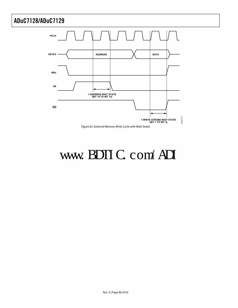
ADuC7128/ADuC7129
Rev. 0 | Page 86 of 92
0602
0-07
2
DATAADDRESS
1 WRITE STROBE WAIT STATE(BIT 7 TO BIT 4)
1 ADDRESS WAIT STATE(BIT 14 TO BIT 12)
HCLK
AD16:0
MSx
AE
WS
Figure 65. External Memory Write Cycle with Wait States
www.BDTIC.com/ADI
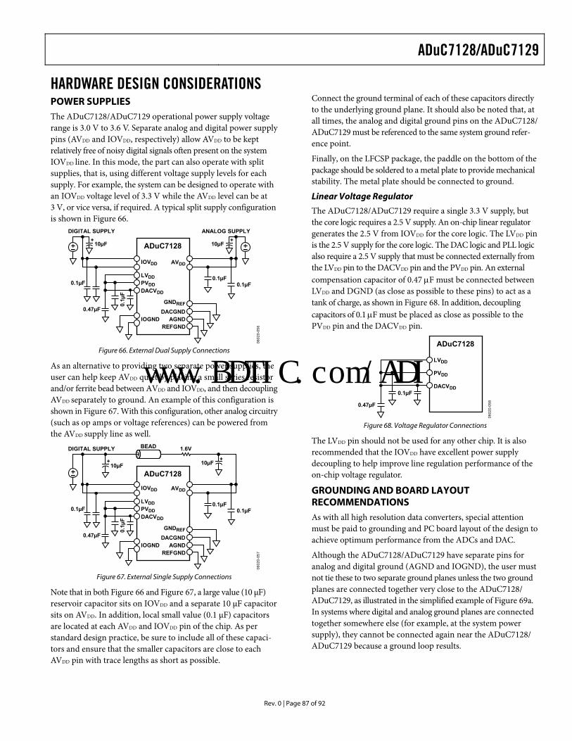
ADuC7128/ADuC7129
Rev. 0 | Page 87 of 92
HARDWARE DESIGN CONSIDERATIONSPOWER SUPPLIES The ADuC7128/ADuC7129 operational power supply voltage range is 3.0 V to 3.6 V. Separate analog and digital power supply pins (AVDD and IOVDD, respectively) allow AVDD to be kept relatively free of noisy digital signals often present on the system IOVDD line. In this mode, the part can also operate with split supplies, that is, using different voltage supply levels for each supply. For example, the system can be designed to operate with an IOVDD voltage level of 3.3 V while the AVDD level can be at 3 V, or vice versa, if required. A typical split supply configuration is shown in Figure 66.
+ANALOG SUPPLY
+DIGITAL SUPPLY
AVDD
GNDREF
DACGNDAGND
REFGND
IOVDD
LVDDPVDDDACVDD
IOGND
ADuC7128 10µF10µF
0.1µ
F
0.1µF
0.47µF
0.1µF0.1µF
0602
0-05
6
Figure 66. External Dual Supply Connections
As an alternative to providing two separate power supplies, the user can help keep AVDD quiet by placing a small series resistor and/or ferrite bead between AVDD and IOVDD, and then decoupling AVDD separately to ground. An example of this configuration is shown in Figure 67. With this configuration, other analog circuitry (such as op amps or voltage references) can be powered from the AVDD supply line as well.
++
DIGITAL SUPPLY
AVDD
GNDREF
DACGNDAGND
REFGND
IOVDD
LVDDPVDDDACVDD
IOGND
ADuC712810µF10µF
0.1µ
F
0.1µF
0.47µF
0.1µF0.1µF
BEAD 1.6V
0602
0-05
7
Figure 67. External Single Supply Connections
Note that in both Figure 66 and Figure 67, a large value (10 μF) reservoir capacitor sits on IOVDD and a separate 10 μF capacitor sits on AVDD. In addition, local small value (0.1 μF) capacitors are located at each AVDD and IOVDD pin of the chip. As per standard design practice, be sure to include all of these capaci-tors and ensure that the smaller capacitors are close to each AVDD pin with trace lengths as short as possible.
Connect the ground terminal of each of these capacitors directly to the underlying ground plane. It should also be noted that, at all times, the analog and digital ground pins on the ADuC7128/ ADuC7129 must be referenced to the same system ground refer-ence point.
Finally, on the LFCSP package, the paddle on the bottom of the package should be soldered to a metal plate to provide mechanical stability. The metal plate should be connected to ground.
Linear Voltage Regulator
The ADuC7128/ADuC7129 require a single 3.3 V supply, but the core logic requires a 2.5 V supply. An on-chip linear regulator generates the 2.5 V from IOVDD for the core logic. The LVDD pin is the 2.5 V supply for the core logic. The DAC logic and PLL logic also require a 2.5 V supply that must be connected externally from the LVDD pin to the DACVDD pin and the PVDD pin. An external compensation capacitor of 0.47 μF must be connected between LVDD and DGND (as close as possible to these pins) to act as a tank of charge, as shown in Figure 68. In addition, decoupling capacitors of 0.1 μF must be placed as close as possible to the PVDD pin and the DACVDD pin.
LVDD
PVDD
DACVDD
ADuC7128
0.1µF
0.47µF
0602
0-05
8
Figure 68. Voltage Regulator Connections
The LVDD pin should not be used for any other chip. It is also recommended that the IOVDD have excellent power supply decoupling to help improve line regulation performance of the on-chip voltage regulator.
GROUNDING AND BOARD LAYOUT RECOMMENDATIONS As with all high resolution data converters, special attention must be paid to grounding and PC board layout of the design to achieve optimum performance from the ADCs and DAC.
Although the ADuC7128/ADuC7129 have separate pins for analog and digital ground (AGND and IOGND), the user must not tie these to two separate ground planes unless the two ground planes are connected together very close to the ADuC7128/ ADuC7129, as illustrated in the simplified example of Figure 69a. In systems where digital and analog ground planes are connected together somewhere else (for example, at the system power supply), they cannot be connected again near the ADuC7128/ ADuC7129 because a ground loop results.
www.BDTIC.com/ADI
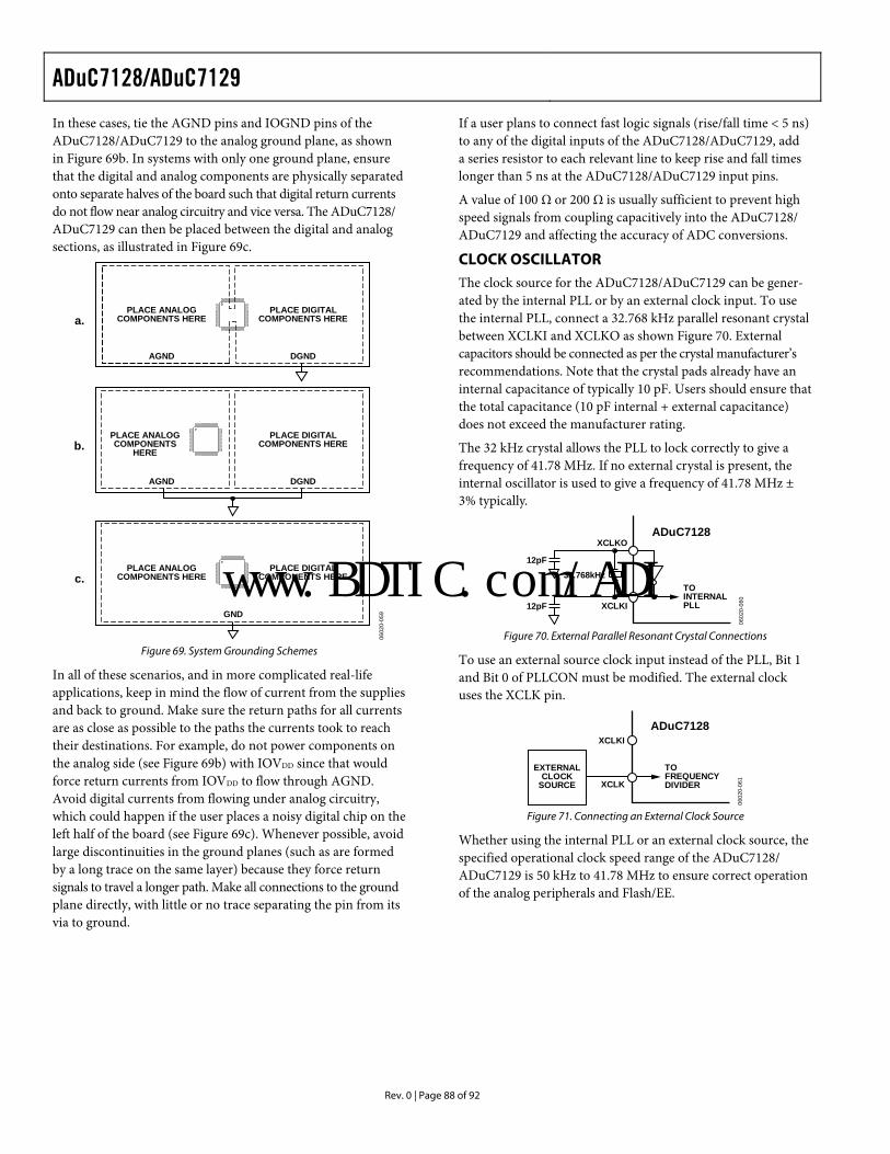
ADuC7128/ADuC7129
Rev. 0 | Page 88 of 92
In these cases, tie the AGND pins and IOGND pins of the ADuC7128/ADuC7129 to the analog ground plane, as shown in Figure 69b. In systems with only one ground plane, ensure that the digital and analog components are physically separated onto separate halves of the board such that digital return currents do not flow near analog circuitry and vice versa. The ADuC7128/ ADuC7129 can then be placed between the digital and analog sections, as illustrated in Figure 69c.
a.PLACE ANALOG
COMPONENTS HEREPLACE DIGITAL
COMPONENTS HERE
AGND DGND
b.PLACE ANALOGCOMPONENTS
HERE
PLACE DIGITALCOMPONENTS HERE
AGND DGND
c.PLACE ANALOG
COMPONENTS HEREPLACE DIGITAL
COMPONENTS HERE
GND
0602
0-05
9
Figure 69. System Grounding Schemes
In all of these scenarios, and in more complicated real-life applications, keep in mind the flow of current from the supplies and back to ground. Make sure the return paths for all currents are as close as possible to the paths the currents took to reach their destinations. For example, do not power components on the analog side (see Figure 69b) with IOVDD since that would force return currents from IOVDD to flow through AGND. Avoid digital currents from flowing under analog circuitry, which could happen if the user places a noisy digital chip on the left half of the board (see Figure 69c). Whenever possible, avoid large discontinuities in the ground planes (such as are formed by a long trace on the same layer) because they force return signals to travel a longer path. Make all connections to the ground plane directly, with little or no trace separating the pin from its via to ground.
If a user plans to connect fast logic signals (rise/fall time < 5 ns) to any of the digital inputs of the ADuC7128/ADuC7129, add a series resistor to each relevant line to keep rise and fall times longer than 5 ns at the ADuC7128/ADuC7129 input pins.
A value of 100 Ω or 200 Ω is usually sufficient to prevent high speed signals from coupling capacitively into the ADuC7128/ ADuC7129 and affecting the accuracy of ADC conversions.
CLOCK OSCILLATOR The clock source for the ADuC7128/ADuC7129 can be gener-ated by the internal PLL or by an external clock input. To use the internal PLL, connect a 32.768 kHz parallel resonant crystal between XCLKI and XCLKO as shown Figure 70. External capacitors should be connected as per the crystal manufacturer’s recommendations. Note that the crystal pads already have an internal capacitance of typically 10 pF. Users should ensure that the total capacitance (10 pF internal + external capacitance) does not exceed the manufacturer rating.
The 32 kHz crystal allows the PLL to lock correctly to give a frequency of 41.78 MHz. If no external crystal is present, the internal oscillator is used to give a frequency of 41.78 MHz ± 3% typically.
ADuC7128
TOINTERNALPLL
12pF
XCLKI
32.768kHz
12pF
XCLKO
0602
0-06
0
Figure 70. External Parallel Resonant Crystal Connections
To use an external source clock input instead of the PLL, Bit 1 and Bit 0 of PLLCON must be modified. The external clock uses the XCLK pin.
ADuC7128
TOFREQUENCYDIVIDER
XCLKI
XCLK
EXTERNALCLOCK
SOURCE
0602
0-06
1
Figure 71. Connecting an External Clock Source
Whether using the internal PLL or an external clock source, the specified operational clock speed range of the ADuC7128/ ADuC7129 is 50 kHz to 41.78 MHz to ensure correct operation of the analog peripherals and Flash/EE.
www.BDTIC.com/ADI
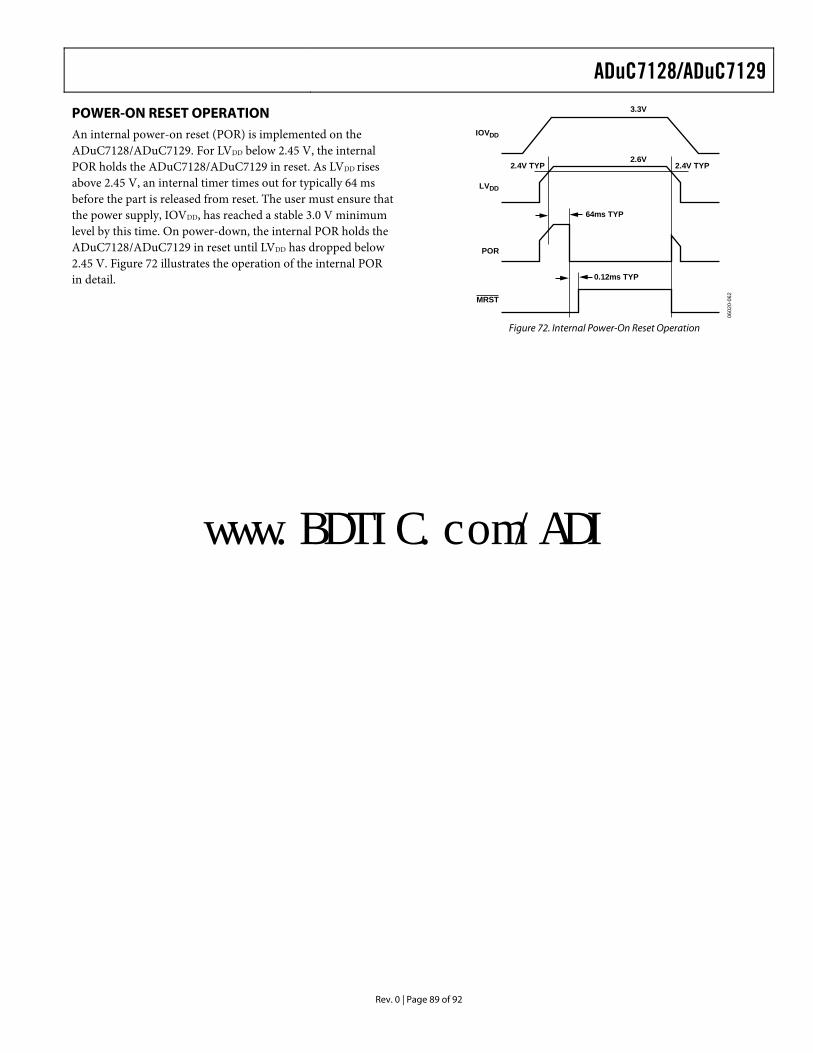
ADuC7128/ADuC7129
Rev. 0 | Page 89 of 92
POWER-ON RESET OPERATION An internal power-on reset (POR) is implemented on the ADuC7128/ADuC7129. For LVDD below 2.45 V, the internal POR holds the ADuC7128/ADuC7129 in reset. As LVDD rises above 2.45 V, an internal timer times out for typically 64 ms before the part is released from reset. The user must ensure that the power supply, IOVDD, has reached a stable 3.0 V minimum level by this time. On power-down, the internal POR holds the ADuC7128/ADuC7129 in reset until LVDD has dropped below 2.45 V. Figure 72 illustrates the operation of the internal POR in detail.
IOVDD
3.3V
2.6V2.4V TYP2.4V TYP
64ms TYP
LVDD
POR
MRST
0.12ms TYP
0602
0-06
2
Figure 72. Internal Power-On Reset Operation
www.BDTIC.com/ADI

ADuC7128/ADuC7129
Rev. 0 | Page 90 of 92
DEVELOPMENT TOOLSAn entry level, low cost development system is available for the ADuC7128/ADuC7129. This system consists of the following PC-based (Windows® compatible) hardware and software development tools.
Hardware
• ADuC7128/ADuC7129 evaluation board • Serial port programming cable • JTAG emulator
Software
• Integrated development environment, incorporating assembler, compiler, and nonintrusive JTAG-based debugger
• Serial downloader software • Example code
Miscellaneous
• CD-ROM documentation
IN-CIRCUIT SERIAL DOWNLOADER The serial downloader is a Windows application that allows the user to serially download an assembled program to the on-chip program Flash/EE memory via the serial port on a standard PC.
www.BDTIC.com/ADI
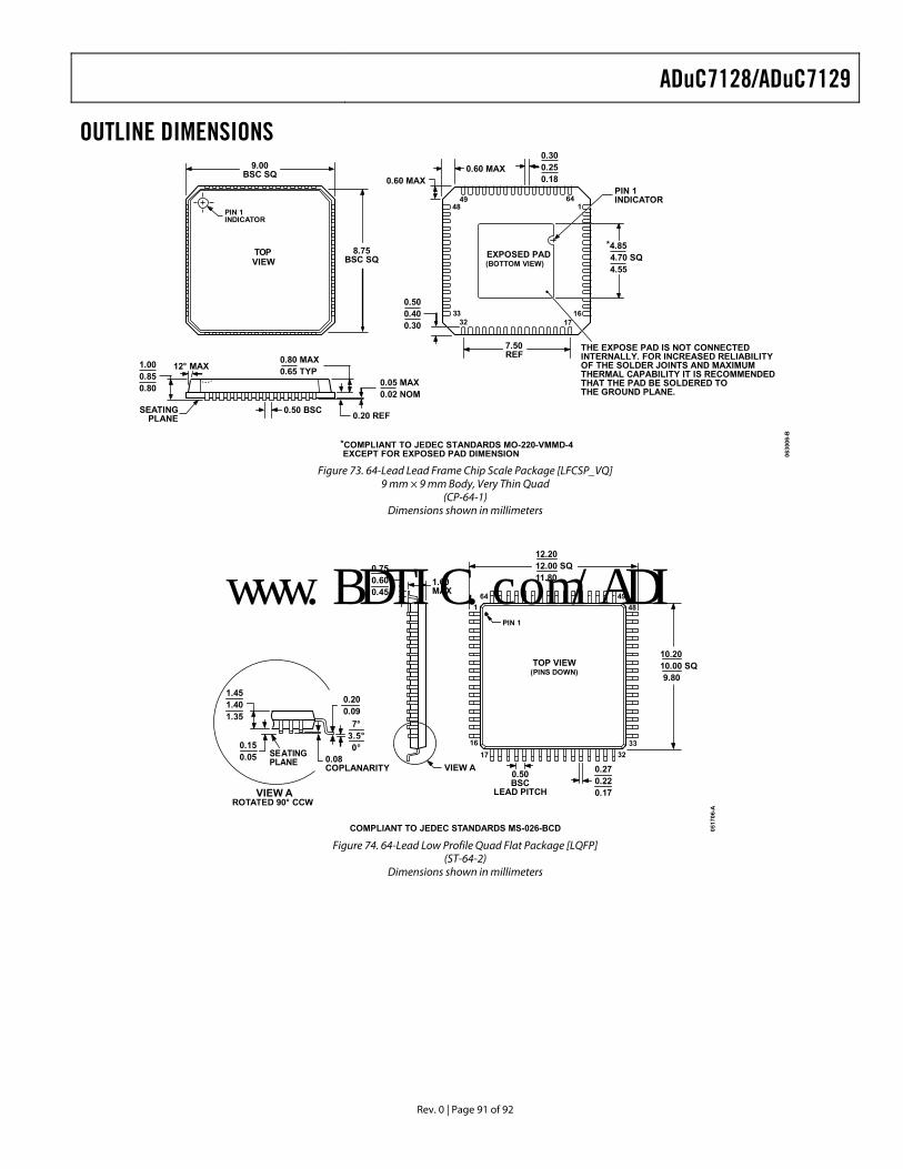
ADuC7128/ADuC7129
Rev. 0 | Page 91 of 92
OUTLINE DIMENSIONS
*COMPLIANT TO JEDEC STANDARDS MO-220-VMMD-4 EXCEPT FOR EXPOSED PAD DIMENSION 06
3006
-B
PIN 1INDICATOR
TOPVIEW
8.75BSC SQ
9.00BSC SQ
164
17
4948
3233
0.500.400.30
0.50 BSC 0.20 REF
12° MAX0.80 MAX0.65 TYP
1.000.850.80
7.50REF
0.05 MAX0.02 NOM
0.60 MAX0.60 MAX
*4.854.70 SQ4.55
EXPOSED PAD(BOTTOM VIEW)
0.300.250.18
SEATINGPLANE
PIN 1INDICATOR
THE EXPOSE PAD IS NOT CONNECTEDINTERNALLY. FOR INCREASED RELIABILITYOF THE SOLDER JOINTS AND MAXIMUMTHERMAL CAPABILITY IT IS RECOMMENDEDTHAT THE PAD BE SOLDERED TOTHE GROUND PLANE.
16
Figure 73. 64-Lead Lead Frame Chip Scale Package [LFCSP_VQ]
9 mm × 9 mm Body, Very Thin Quad (CP-64-1)
Dimensions shown in millimeters
COMPLIANT TO JEDEC STANDARDS MS-026-BCD 0517
06-A
TOP VIEW(PINS DOWN)
1
1617
3332
484964
0.270.220.17
0.50BSC
LEAD PITCH
12.2012.00 SQ11.80
PIN 1
1.60MAX
0.750.600.45
10.2010.00 SQ9.80
VIEW A
0.20 0.09
1.451.401.35
0.08COPLANARITY
VIEW AROTATED 90° CCW
SEATINGPLANE
0.150.05
7°3.5°0°
Figure 74. 64-Lead Low Profile Quad Flat Package [LQFP]
(ST-64-2) Dimensions shown in millimeters
www.BDTIC.com/ADI
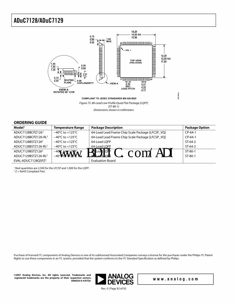
ADuC7128/ADuC7129
Rev. 0 | Page 92 of 92
COMPLIANT TO JEDEC STANDARDS MS-026-BDD 0517
06-A
0.150.05
1.45 1.40 1.35
0.20 0.09
0.08COPLANARITY
VIEW AROTATED 90° CCW
SEATINGPLANE
7°3.5°0°
TOP VIEW(PINS DOWN)
1
2141
40
606180
20
0.50BSC
LEAD PITCH
0.270.220.17
1.60MAX
0.750.600.45
VIEW A
PIN 1
14.2014.00 SQ13.80
12.2012.00 SQ11.80
Figure 75. 80-Lead Low Profile Quad Flat Package [LQFP]
(ST-80-1) Dimensions shown in millimeters
ORDERING GUIDE Model1 Temperature Range Package Description Package Option ADUC7128BCPZ1262 −40°C to +125°C 64-Lead Lead Frame Chip Scale Package [LFCSP_VQ] CP-64-1 ADUC7128BCPZ126-RL2 −40°C to +125°C 64-Lead Lead Frame Chip Scale Package [LFCSP_VQ] CP-64-1 ADUC7128BSTZ1262 −40°C to +125°C 64-Lead LQFP ST-64-2 ADUC7128BSTZ126-RL2 −40°C to +125°C 64-Lead LQFP ST-64-2 ADUC7129BSTZ1262 −40°C to +125°C 80-Lead LQFP ST-80-1 ADUC7129BSTZ126-RL2 −40°C to +125°C 80-Lead LQFP ST-80-1 EVAL-ADUC7128QSPZ2 Evaluation Board 1 Reel quantities are 2,500 for the LFCSP and 1,000 for the LQFP. 2 Z = RoHS Compliant Part.
Purchase of licensed I2C components of Analog Devices or one of its sublicensed Associated Companies conveys a license for the purchaser under the Philips I2C Patent Rights to use these components in an I2C system, provided that the system conforms to the I2C Standard Specification as defined by Philips.
©2007 Analog Devices, Inc. All rights reserved. Trademarks and registered trademarks are the property of their respective owners. D06020-0-4/07(0)
www.BDTIC.com/ADI