ADSP-BF537 EZ-KIT Lite Evaluation System Manual · ADSP-BF537 EZ-KIT Lite Evaluation System Manual...
91
ADSP-BF537 EZ-KIT Lite ® Evaluation System Manual Revision 1.1, August 2005 Part Number 82-000865-01 Analog Devices, Inc. One Technology Way Norwood, Mass. 02062-9106 a
Transcript of ADSP-BF537 EZ-KIT Lite Evaluation System Manual · ADSP-BF537 EZ-KIT Lite Evaluation System Manual...
ADSP-BF537 EZ-KIT Lite®
Evaluation System Manual
Revision 1.1, August 2005
Part Number82-000865-01
Analog Devices, Inc.One Technology WayNorwood, Mass. 02062-9106 a

Copyright Information© 2005 Analog Devices, Inc., ALL RIGHTS RESERVED. This docu-ment may not be reproduced in any form without prior, express written consent from Analog Devices, Inc.
Printed in the USA.
Limited WarrantyThe EZ-KIT Lite evaluation system is warranted against defects in materi-als and workmanship for a period of one year from the date of purchase from Analog Devices or from an authorized dealer.
DisclaimerAnalog Devices, Inc. reserves the right to change this product without prior notice. Information furnished by Analog Devices is believed to be accurate and reliable. However, no responsibility is assumed by Analog Devices for its use; nor for any infringement of patents or other rights of third parties which may result from its use. No license is granted by impli-cation or otherwise under the patent rights of Analog Devices, Inc.
Trademark and Service Mark NoticeThe Analog Devices logo, VisualDSP++, the VisualDSP++ logo, Blackfin, the CROSSCORE logo, and EZ-KIT Lite are registered trademarks of Analog Devices, Inc.
All other brand and product names are trademarks or service marks of their respective owners.

Regulatory Compliance The ADSP-BF537 EZ-KIT Lite evaluation system has been certified to comply with the essential requirements of the European EMC directive 89/336/EEC (inclusive 93/68/EEC) and, therefore, carries the “CE” mark.
The ADSP-BF537 EZ-KIT Lite evaluation system had been appended to Analog Devices Development Tools Technical Construction File refer-enced “DSPTOOLS1” dated December 21, 1997 and was awarded CE Certification by an appointed European Competent Body and is on file.
The EZ-KIT Lite evaluation system contains ESD (electrostatic discharge) sensitive devices. Electro-static charges readily accumulate on the human body and equipment and can discharge without detection. Permanent damage may occur on devices subjected to high-energy discharges. Proper ESD precautions are recommended to avoid performance degradation or loss of functionality. Store unused EZ-KIT Lite boards in the protective shipping package.

CONTENTS
PREFACE
Purpose of This Manual ................................................................ xiii
Intended Audience ......................................................................... xiv
Manual Contents ........................................................................... xiv
What’s New in This Manual ............................................................ xv
Technical or Customer Support ....................................................... xv
Supported Processors ...................................................................... xvi
Product Information ...................................................................... xvi
MyAnalog.com ......................................................................... xvi
Processor Product Information ................................................. xvii
Related Documents ................................................................. xvii
Online Technical Documentation ............................................. xix
Accessing Documentation From VisualDSP++ ...................... xix
Accessing Documentation From Windows ............................. xx
Accessing Documentation From Web .................................... xx
Printed Manuals ........................................................................ xx
VisualDSP++ Documentation Set ......................................... xxi
Hardware Tools Manuals ...................................................... xxi
Processor Manuals ................................................................ xxi
ADSP-BF537 EZ-KIT Lite Evaluation System Manual v

CONTENTS
Data Sheets ......................................................................... xxi
Notation Conventions .................................................................. xxii
USING EZ-KIT LITE
Package Contents ......................................................................... 1-2
Default Configuration .................................................................. 1-3
Installation and Session Startup ..................................................... 1-5
Evaluation License Restrictions ..................................................... 1-6
Memory Map ............................................................................... 1-6
SDRAM Interface ......................................................................... 1-8
Flash Memory .............................................................................. 1-9
CAN Interface ............................................................................ 1-10
Ethernet Interface ....................................................................... 1-11
ELVIS Interface .......................................................................... 1-11
Audio Interface ........................................................................... 1-12
LEDs and Push Buttons .............................................................. 1-13
Example Programs ...................................................................... 1-13
Background Telemetry Channel .................................................. 1-14
EZ-KIT LITE HARDWARE REFERENCE
System Architecture ...................................................................... 2-2
External Bus Interface Unit ..................................................... 2-3
SPORT0 Audio Interface ........................................................ 2-3
SPI Interface ........................................................................... 2-4
Programmable Flags (PFs) ....................................................... 2-4
vi ADSP-BF537 EZ-KIT Lite Evaluation System Manual
CONTENTS
UART Port .............................................................................. 2-7
Expansion Interface ................................................................. 2-7
JTAG Emulation Port .............................................................. 2-8
Jumper and Switch Settings ........................................................... 2-8
CAN Enable Switch (SW2) ...................................................... 2-8
Ethernet Mode Select Switch (SW3) ........................................ 2-9
UART Enable Switch (SW4) .................................................... 2-9
Push Button Enable Switch (SW5) ......................................... 2-10
Flash Enable Switch (SW6) .................................................... 2-10
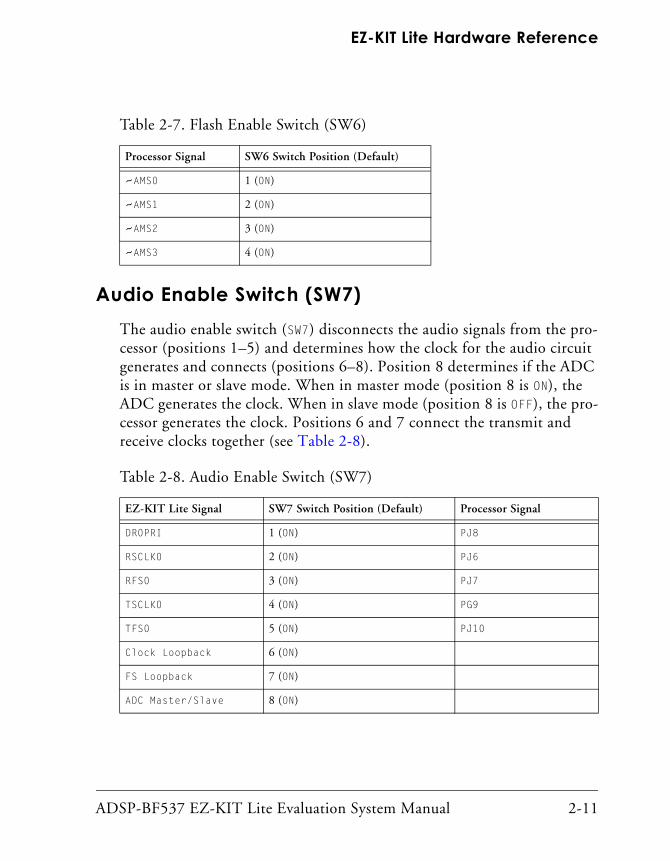
Audio Enable Switch (SW7) .................................................. 2-11
Boot Mode Select Switch (SW16) .......................................... 2-12
3V Power Selection Jumper (JP3) ........................................... 2-12
Expansion Interface Voltage Selection Jumper (JP5) ............... 2-13
UART Loop Jumper (JP9) ..................................................... 2-13
ELVIS Oscilloscope Configuration Switch (SW1) ................... 2-14
ELVIS Function Generator Configuration Switch (SW8) ........ 2-14
ELVIS Voltage Selection Jumper (JP6) ................................... 2-15
ELVIS Select Jumper (JP8) .................................................... 2-16
LEDs and Push Buttons .............................................................. 2-17
Reset Push Button (SW9) ...................................................... 2-17
Programmable Flag Push Buttons (SW10–13) ........................ 2-18
Power LED (LED7) ............................................................... 2-18
Reset LEDs (LED8 and LED9) .............................................. 2-18
User LEDs (LED1–6) ............................................................ 2-19
ADSP-BF537 EZ-KIT Lite Evaluation System Manual vii

CONTENTS
USB Monitor LED (LED10) ................................................. 2-19
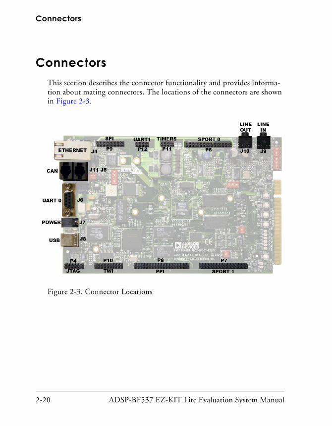
Connectors ................................................................................. 2-20
Audio Connectors (J9 and J10) ............................................. 2-21
CAN Connectors (J5 and J11) .............................................. 2-21
Ethernet Connector (J4) ....................................................... 2-21
RS-232 Connector (J6) ......................................................... 2-22
Power Connector (J7) ........................................................... 2-22
Expansion Interface Connectors (J1–3) .................................. 2-23
JTAG Connector (P4) ........................................................... 2-23
SPORT0 Connector (P6) ...................................................... 2-24
SPORT1 Connector (P7) ...................................................... 2-24
PPI Connector (P8) .............................................................. 2-24
SPI Connector (P9) ............................................................... 2-25
Two-Wire Interface Connector (P10) ..................................... 2-25
TIMERS Connector (P11) .................................................... 2-25
UART1 Connector (P12) ...................................................... 2-26
BILL OF MATERIALS
INDEX
viii ADSP-BF537 EZ-KIT Lite Evaluation System Manual
PREFACE
Thank you for purchasing the ADSP-BF537 EZ-KIT Lite®, Analog
Devices, Inc. evaluation system for Blackfin® processors.The Blackfin processor family embodies a new type of embedded proces-sor designed specifically to meet the computational demands and power constraints of today’s embedded audio, video, and communications appli-cations. They deliver breakthrough signal-processing performance and power efficiency within a reduced instruction set computing (RISC) pro-gramming model.
Blackfin processors support a media instruction set computing (MISC) architecture. This architecture is the natural merging of RISC, media functions, and digital signal processing (DSP) characteristics. Blackfin processors deliver signal-processing performance in a microprocessor-like environment.
Based on the Micro Signal Architecture (MSA), Blackfin processors com-bine a 32-bit RISC instruction set, dual 16-bit multiply accumulate (MAC) DSP functionality, and 8-bit video processing performance that had previously been the exclusive domain of very-long instruction word (VLIW) media processors.
ADSP-BF537 EZ-KIT Lite Evaluation System Manual ix

The evaluation board is designed to be used in conjunction with the Visu-alDSP++® development environment to test the capabilities of the ADSP-BF537 Blackfin processors. The VisualDSP++ development envi-ronment gives you the ability to perform advanced application code development and debug, such as:
• Create, compile, assemble, and link application programs written in C++, C and ADSP-BF537 assembly
• Load, run, step, halt, and set breakpoints in application program
• Read and write data and program memory
• Read and write core and peripheral registers
• Plot memory
Access to the ADSP-BF537 processor from a personal computer (PC) is achieved through a USB port or an optional JTAG emulator. The USB interface gives unrestricted access to the ADSP-BF537 processor and the evaluation board peripherals. Analog Devices JTAG emulators offer faster communication between the host PC and target hardware. Analog Devices carries a wide range of in-circuit emulation products. To learn more about Analog Devices emulators and processor development tools, go to http://www.analog.com/dsp/tools/.
ADSP-BF537 EZ-KIT Lite provides example programs to demonstrate the capabilities of the evaluation board.
x ADSP-BF537 EZ-KIT Lite Evaluation System Manual

Preface
The ADSP-BF537 EZ-KIT Lite installation is part of the Visu-alDSP++ installation. The EZ-KIT Lite is a licensed product that offers an unrestricted evaluation license for the first 90 days. Once the initial unrestricted 90-day evaluation license expires:
• VisualDSP++ allows a connection to the ADSP-BF537 EZ-KIT Lite via the USB debug agent interface only. Connections to simu-lators and emulation products are no longer allowed.
• The linker restricts a users program to 20 KB of internal memory for code space with no restrictions for data space.
The board features:
• Analog Devices ADSP-BF537 processor
Core performance to 600 MHzExternal bus performance to 133 MHz182-pin mini-BGA package25 MHz crystal
• Synchronous dynamic random access memory (SDRAM)
MT48LC32M8 – 64 MB (8M x8-bits x 4 banks) x 2 chips
• Flash memory
4MB (2M x 16-bits)
• Analog audio interface
AD1871 96 kHz analog-to-digital codec (ADC)AD1854 96 kHz digital-to-audio codec (DAC)1 input stereo jack1 output stereo jack
ADSP-BF537 EZ-KIT Lite Evaluation System Manual xi
• Ethernet interface
10-BaseT (10 Mbits/sec) and 100-BaseT (100 Mbits/sec) Ethernet Media Access Controller (MAC)SMSC LAN83C185 device
• Controller Area Network (CAN) interface
Philips TJA1041 high-speed CAN transceiver
• National Instruments Educational Laboratory Virtual Instrumen-tation Suite (ELVIS) interface
LabVIEW™-based virtual instrumentsMultifunction data acquisition deviceBench-top workstation and prototype board
• Universal asynchronous receiver/transmitter (UART)
ADM3202 RS-232 line driver/receiverDB9 female connector
• LEDs
10 LEDs: 1 power (green), 1 board reset (red), 1 USB (red), 6 general purpose (amber), and 1 USB monitor (amber)
• Push buttons
5 push buttons: 1 reset, 4 programmable flags with debounce logic
• Expansion interface
All processor signals
• Other features
JTAG ICE 14-pin header
xii ADSP-BF537 EZ-KIT Lite Evaluation System Manual

Preface
The EZ-KIT Lite board has flash memory with a total of 4 MB. The flash memory can be used to store user-specific boot code, allowing the board to run as a stand-alone unit. For more information, see “Flash Memory” on page 1-9. The board also has 64 MB of SDRAM, which can be used by the user at runtime.
SPORT0 interfaces with the audio circuit, facilitating development of audio signal processing applications. SPORT0 also connects to an off-board con-nector for communication with other serial devices. For information about SPORT0, see “SPORT0 Audio Interface” on page 2-3.
The UART of the processor connects to an RS-232 line driver and a DB9 female connector, providing an interface to a PC or other serial device.
Additionally, the EZ-KIT Lite board provides access to all of the proces-sor’s peripheral ports. Access is provided in the form of a three-connector expansion interface. For information about the expansion interface, see “Expansion Interface” on page 2-7.
Purpose of This Manual The ADSP-BF537 EZ-KIT Lite Evaluation System Manual provides instructions for installing the product hardware (board). The text describes the operation and configuration of the board components and provides guidelines for running your own code on the ADSP-BF537 EZ-KIT Lite. Finally, a schematic and a bill of materials are provided as a reference for future designs.
EZ-KIT Lite users should use this manual in conjunction with the Getting Started with ADSP-BF537 EZ-KIT Lite, which familiarizes users with the hardware capabilities of the evaluation system and demonstrates how to access these capabilities in the VisualDSP++ environment.
The product software installation is detailed in the VisualDSP++ Installa-tion Quick Reference Card.
ADSP-BF537 EZ-KIT Lite Evaluation System Manual xiii
Intended Audience
Intended AudienceThe primary audience for this manual is a programmer who is familiar with Analog Devices processors. This manual assumes that the audience has a working knowledge of the appropriate processor architecture and instruction set. Programmers who are unfamiliar with Analog Devices processors can use this manual but should supplement it with other texts (such as the ADSP-BF537 Blackfin Processor Hardware Reference and Blackfin Processor Instruction Set Reference) that describe your target architecture.
Programmers who are unfamiliar with VisualDSP++ should refer to the VisualDSP++ online Help and user’s or getting started guides. For the locations of these documents, see “Related Documents”.
Manual ContentsThe manual consists of:
• Chapter 1, “Using EZ-KIT Lite” on page 1-1Describes the EZ-KIT Lite functionality from a programmer’s per-spective and provides an easy-to-access memory map.
• Chapter 2, “EZ-KIT Lite Hardware Reference” on page 2-1Provides information on the EZ-KIT Lite hardware components.
• Appendix A, “Bill Of Materials” on page A-1Provides a list of components used to manufacture the EZ-KIT Lite board.
xiv ADSP-BF537 EZ-KIT Lite Evaluation System Manual

Preface
• Appendix B, “Schematics” on page B-1Provides the resources to allow EZ-KIT Lite board-level debugging or to use as a reference design.
This appendix is not part of the online Help. The online Help viewers should go to the PDF version of the ADSP-BF537 EZ-KIT Lite Evaluation System Manual located in the Docs\EZ-KIT Lite Manuals folder on the installation CD to see the schematics. Alter-natively, the schematics can be found on the Analog Devices Web site, www.analog.com/processors.
What’s New in This Manual This is the second edition of the ADSP-BF537 EZ-KIT Lite Evaluation System Manual. The new edition includes the updated board’s schematics and bill of materials.
Technical or Customer SupportYou can reach Analog Devices, Inc. Customer Support in the following ways:
• Visit the Embedded Processing and DSP products Web site athttp://www.analog.com/processors/technicalSupport
• E-mail tools questions [email protected]
• E-mail processor questions [email protected] (World wide support)
[email protected] (Europe support)
[email protected] (China support)
• Phone questions to 1-800-ANALOGD
ADSP-BF537 EZ-KIT Lite Evaluation System Manual xv
Supported Processors
• Contact your Analog Devices, Inc. local sales office or authorized distributor
• Send questions by mail to:Analog Devices, Inc.
One Technology Way
P.O. Box 9106
Norwood, MA 02062-9106
USA
Supported ProcessorsThis evaluation system supports the Analog Devices ADSP-BF537 Black-fin embedded processors.
Product InformationYou can obtain product information from the Analog Devices Web site, from the product CD-ROM, or from the printed publications (manuals).
Analog Devices is online at www.analog.com. Our Web site provides infor-mation about a broad range of products—analog integrated circuits, amplifiers, converters, and digital signal processors.
MyAnalog.comMyAnalog.com is a free feature of the Analog Devices Web site that allows customization of a Web page to display only the latest information on products you are interested in. You can also choose to receive weekly e-mail notifications containing updates to the Web pages that meet your interests. MyAnalog.com provides access to books, application notes, data sheets, code examples, and more.
xvi ADSP-BF537 EZ-KIT Lite Evaluation System Manual

Preface
Registration:
Visit www.myanalog.com to sign up. Click Register to use MyAnalog.com. Registration takes about five minutes and serves as means for you to select the information you want to receive.
If you are already a registered user, just log on. Your user name is your e-mail address.
Processor Product InformationFor information on embedded processors and DSPs, visit our Web site at www.analog.com/processors, which provides access to technical publica-tions, data sheets, application notes, product overviews, and product announcements.
You may also obtain additional information about Analog Devices and its products in any of the following ways.
• E-mail questions or requests for information to [email protected] (World wide support) [email protected] (Europe support) [email protected] (China support)
• Fax questions or requests for information to1-781-461-3010 (North America)+49-89-76903-157 (Europe)
Related DocumentsFor information on product related development software, see the follow-ing publications.
If you plan to use the EZ-KIT Lite board in conjunction with a JTAG emulator, also refer to the documentation that accompanies the emulator.
ADSP-BF537 EZ-KIT Lite Evaluation System Manual xvii

Product Information
All documentation is available online. Most documentation is available in printed form.
Visit the Technical Library Web site to access all processor and tools man-uals and data sheets: http://www.analog.com/processors/resources/technicalLibrary.
Table -1. Related Processor Publications
Title Description
ADSP-BF536/ADSP-BF537 Embedded Processor Data Sheet
General functional description, pinout, and timing.
ADSP-BF537 Blackfin Processor Hardware Refer-ence
Description of internal processor architec-ture and all register functions.
Blackfin Processor Programming Reference Description of all allowed processor assem-bly instructions.
Table -2. Related VisualDSP++ Publications
Title Description
ADSP-BF537 EZ-KIT Lite Evaluation System Manual
Description of the hardware capabilities of the evaluation system; description of how to access these capabilities in the VisualDSP++ environment.
VisualDSP++ User’s Guide Description of VisualDSP++ features and usage.
VisualDSP++ Assembler and Preprocessor Manuals Description of the assembler function and commands.
VisualDSP++ C/C++ Complier and Library Man-ual for Blackfin Processors
Description of the complier function and commands for Blackfin processors.
VisualDSP++ Linker and Utilities Manual Description of the linker function and com-mands.
VisualDSP++ Loader Manual Description of the loader/splitter function and commands.
xviii ADSP-BF537 EZ-KIT Lite Evaluation System Manual

Preface
Online Technical Documentation Online documentation comprises the VisualDSP++ Help system, software tools manuals, hardware tools manuals, processor manuals, the Dinkum Abridged C++ library, and Flexible License Manager (FlexLM) network license manager software documentation. You can easily search across the entire VisualDSP++ documentation set for any topic of interest. For easy printing, supplementary .PDF files of most manuals are provided in the Docs folder on the VisualDSP++ installation CD.
Each documentation file type is described as follows.
If documentation is not installed on your system as part of the software installation, you can add it from the VisualDSP++ CD at any time by run-ning the Tools installation. Access the online documentation from the VisualDSP++ environment, Windows® Explorer, or the Analog Devices Web site.
Accessing Documentation From VisualDSP++
To view VisualDSP++ Help, click on the Help menu item or go to the Windows task bar and navigate to the VisualDSP++ documentation via the Start menu.
File Description
.CHM Help system files and manuals in Help format
.HTM or
.HTMLDinkum Abridged C++ library and FlexLM network license manager software doc-umentation. Viewing and printing the .HTML files requires a browser, such as Internet Explorer 4.0 (or higher).
.PDF VisualDSP++ and processor manuals in Portable Documentation Format (PDF). Viewing and printing the .PDF files requires a PDF reader, such as Adobe Acrobat Reader (4.0 or higher).
ADSP-BF537 EZ-KIT Lite Evaluation System Manual xix

Product Information
To view ADSP-BF537 EZ-KIT Lite Help, which is part of the Visu-alDSP++ Help system, use the Contents or Search tab of the Help window.
Accessing Documentation From Windows
In addition to any shortcuts you may have constructed, there are many ways to open VisualDSP++ online Help or the supplementary documenta-tion from Windows.
Help system files (.CHM) are located in the Help folder, and .PDF files are located in the Docs folder of your VisualDSP++ installation CD-ROM. The Docs folder also contains the Dinkum Abridged C++ library and the FlexLM network license manager software documentation.
Your software installation kit includes online Help as part of the Win-dows® interface. These help files provide information about VisualDSP++ and the ADSP-BF537 EZ-KIT Lite evaluation system.
Accessing Documentation From Web
Download manuals at the following Web site: http://www.analog.com/processors/resources/technicalLibrary/man-
uals.
Select a processor family and book title. Download archive (.ZIP) files, one for each manual. Use any archive management software, such as WinZip, to decompress downloaded files.
Printed ManualsFor general questions regarding literature ordering, call the Literature Center at 1-800-ANALOGD (1-800-262-5643) and follow the prompts.
xx ADSP-BF537 EZ-KIT Lite Evaluation System Manual
Preface
VisualDSP++ Documentation Set
To purchase VisualDSP++ manuals, call 1-603-883-2430. The manuals may be purchased only as a kit.
If you do not have an account with Analog Devices, you are referred to Analog Devices distributors. For information on our distributors, log onto http://www.analog.com/salesdir/continent.asp.
Hardware Tools Manuals
To purchase EZ-KIT Lite and In-Circuit Emulator (ICE) manuals, call 1-603-883-2430. The manuals may be ordered by title or by product number located on the back cover of each manual.
Processor Manuals
Hardware reference and instruction set reference manuals may be ordered through the Literature Center at 1-800-ANALOGD (1-800-262-5643), or downloaded from the Analog Devices Web site. Manuals may be ordered by title or by product number located on the back cover of each manual.
Data Sheets
All data sheets (preliminary and production) may be downloaded from the Analog Devices Web site. Only production (final) data sheets (Rev. 0, A, B, C, and so on) can be obtained from the Literature Center at 1-800-ANALOGD (1-800-262-5643); they also can be downloaded from the Web site.
To have a data sheet faxed to you, call the Analog Devices Faxback System at 1-800-446-6212. Follow the prompts and a list of data sheet code numbers will be faxed to you. If the data sheet you want is not listed, check for it on the Web site.
ADSP-BF537 EZ-KIT Lite Evaluation System Manual xxi

Notation Conventions
Notation ConventionsText conventions used in this manual are identified and described as follows.
Example Description
Close command (File menu)
Titles in reference sections indicate the location of an item within the VisualDSP++ environment’s menu system (for example, the Close com-mand appears on the File menu).
{this | that} Alternative required items in syntax descriptions appear within curly brackets and separated by vertical bars; read the example as this or that. One or the other is required.
[this | that] Optional items in syntax descriptions appear within brackets and sepa-rated by vertical bars; read the example as an optional this or that.
[this,…] Optional item lists in syntax descriptions appear within brackets delim-ited by commas and terminated with an ellipse; read the example as an optional comma-separated list of this.
.SECTION Commands, directives, keywords, and feature names are in text with letter gothic font.
filename Non-keyword placeholders appear in text with italic style format.
Note: For correct operation, ...A Note provides supplementary information on a related topic. In the online version of this book, the word Note appears instead of this symbol.
Caution: Incorrect device operation may result if ...Caution: Device damage may result if ... A Caution identifies conditions or inappropriate usage of the product that could lead to undesirable results or product damage. In the online version of this book, the word Caution appears instead of this symbol.
Warning: Injury to device users may result if ... A Warning identifies conditions or inappropriate usage of the product that could lead to conditions that are potentially hazardous for the devices users. In the online version of this book, the word Warning appears instead of this symbol.
xxii ADSP-BF537 EZ-KIT Lite Evaluation System Manual

Preface
Additional conventions, which apply only to specific chapters, may appear throughout this document.
ADSP-BF537 EZ-KIT Lite Evaluation System Manual xxiii

Notation Conventions
xxiv ADSP-BF537 EZ-KIT Lite Evaluation System Manual
1 USING EZ-KIT LITE
This chapter provides specific information to assist you with development
of programs for the ADSP-BF537 EZ-KIT Lite evaluation system.The information appears in the following sections.
• “Package Contents” on page 1-2Lists the items contained in your ADSP-BF537 EZ-KIT Lite package.
• “Default Configuration” on page 1-3Shows the default configuration of the ADSP-BF537 EZ-KIT Lite.
• “Installation and Session Startup” on page 1-5Instructs how to start a new or open an existing ADSP-BF537 EZ-KIT Lite session using VisualDSP++.
• “Evaluation License Restrictions” on page 1-6Describes the restrictions of the VisualDSP++ demo license shipped with the EZ-KIT Lite.
• “Memory Map” on page 1-6Defines the ADSP-BF537 EZ-KIT Lite board’s memory map.
• “SDRAM Interface” on page 1-8·Defines the register values to configure the on-board SDRAM.
• “Flash Memory” on page 1-9Describes the on-board flash memory.
• “CAN Interface” on page 1-10Describes the on-board Controller Area Network (CAN) interface.
ADSP-BF537 EZ-KIT Lite Evaluation System Manual 1-1
Package Contents
• “Ethernet Interface” on page 1-11Describes the on-board Fast Ethernet Media Access Controller (MAC) interface.
• “ELVIS Interface” on page 1-11Describes the on-board National Instruments Educational Labora-tory Virtual Instrumentation Suite (NI ELVIS) interface.
• “Audio Interface” on page 1-12Describes the on-board audio circuit.
• “LEDs and Push Buttons” on page 1-13Describes the board’s general-purpose IO pins and buttons.
• “Background Telemetry Channel” on page 1-14Highlights the advantages of the background telemetry channel (BTC) feature of VisualDSP++.
For information on the graphical user interface, including the boot load-ing, target options, and other facilities of the EZ-KIT Lite system, refer to the online Help.
For more detailed information about programming the ADSP-BF537 Blackfin processor, see the documents referred to as “Related Documents”.
Package ContentsYour ADSP-BF537 EZ-KIT Lite evaluation system package contains the following items.
• ADSP-BF537 EZ-KIT Lite board
• VisualDSP++ Installation Quick Reference Card
1-2 ADSP-BF537 EZ-KIT Lite Evaluation System Manual
Using EZ-KIT Lite
• CD containing:
VisualDSP++ software
ADSP-BF537 EZ-KIT Lite debug software
USB driver files
Example programs
ADSP-BF537 EZ-KIT Lite Evaluation System Manual (this document)
• Universal 7V DC power supply
• 7-foot Ethernet crossover cable
• 7-foot Ethernet patch cable
• 6-foot 3.5 mm male-to-male audio cable
• 3.5 mm headphones
• 10-foot USB 2.0 cable
• Registration card (please fill out and return)
If any item is missing, contact the vendor where you purchased your EZ-KIT Lite or contact Analog Devices, Inc.
Default ConfigurationThe ADSP-BF537 EZ-KIT Lite board is designed to run outside your per-sonal computer as a stand-alone unit. You do not have to open your computer case.
ADSP-BF537 EZ-KIT Lite Evaluation System Manual 1-3

Default Configuration
When removing the EZ-KIT Lite board from the package, handle the board carefully to avoid the discharge of static electricity, which may dam-age some components. Figure 1-1 shows the default jumper settings, switches, connector locations, and LEDs used in installation. Confirm that your board is set up in the default configuration before using the board.
The EZ-KIT Lite evaluation system contains ESD (electrostatic discharge) sensitive devices. Electrostatic charges readily accumulate on the human body and equipment and can discharge without detection. Per-manent damage may occur on devices subjected to high-energy discharges. Proper ESD precautions are recommended to avoid performance degradation or loss of functionality. Store unused EZ-KIT Lite boards in the protective shipping package.
Figure 1-1. EZ-KIT Lite Hardware Setup
1-4 ADSP-BF537 EZ-KIT Lite Evaluation System Manual
Using EZ-KIT Lite
Installation and Session StartupFor correct operation, install the software and hardware in the order presented in the VisualDSP++ Installation Quick Reference Card.
1. Verify that the yellow USB monitor LED (LED10, located near the USB connector) is lit. This signifies that the board is communicat-ing properly with the host PC and is ready to run VisualDSP++.
2. From the Start menu, navigate to the VisualDSP++ environment via the Programs menu.
If you are running VisualDSP++ for the first time, the New Session dialog box appears on the screen (skip the rest of the procedure and go to step 3).
If you have run VisualDSP++ previously, the last opened session appears on the screen.
To switch to another session, via the Session List dialog box, hold down the Ctrl key while starting VisualDSP++ (go to step 5).
3. In Debug target, select Blackfin Emulators/EZ-KIT Lites.In Platform, select the appropriate EZ-KIT Lite via a debug agent(ADSP-BF537 EZ-KIT Lite via Debug Agent). In Session name, type a new name or accept the default.
4. Click OK to return to the Session List.
5. Highlight the session and click Activate.
ADSP-BF537 EZ-KIT Lite Evaluation System Manual 1-5
Evaluation License Restrictions
Evaluation License RestrictionsThe ADSP-BF537 EZ-KIT Lite installation is part of the VisualDSP++ installation. The EZ-KIT Lite is a licensed product that offers an unre-stricted evaluation license for the first 90 days. Once the initial unrestricted 90-day evaluation license expires:
• VisualDSP++ allows a connection to the ADSP-BF537 EZ-KIT Lite via the USB debug agent interface only. Connections to simu-lators and emulation products are no longer allowed.
• The linker restricts a users program to 20 KB of internal memory for code space with no restrictions for data space.
The EZ-KIT Lite hardware must be connected and powered up to use VisualDSP++ with a valid evaluation or permanent license.
Refer to the VisualDSP++ Installation Quick Reference Card for details.
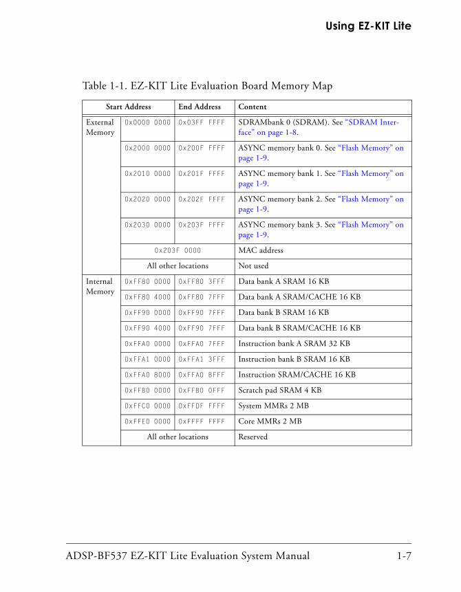
Memory MapThe ADSP-BF537 processor has internal SRAM that can be used for instruction or data storage. The configuration of internal SRAM is detailed in the ADSP-BF537 Blackfin Processor Hardware Reference.
The ADSP-BF537 EZ-KIT Lite board includes two types of external memory, SDRAM and flash.
The size of the SDRAM is 64 Mbytes (32M x 16-bit). The processor’s memory select pin, ~SMS0, is configured for the SDRAM.
The size of the flash memory is 4 Mbytes (2M x 16-bits). The processor’s asynchronous memory select pins ~AMS3–0 are configured for the flash.
1-6 ADSP-BF537 EZ-KIT Lite Evaluation System Manual
Using EZ-KIT Lite
Table 1-1. EZ-KIT Lite Evaluation Board Memory Map
Start Address End Address Content
External Memory
0x0000 0000 0x03FF FFFF SDRAMbank 0 (SDRAM). See “SDRAM Inter-face” on page 1-8.
0x2000 0000 0x200F FFFF ASYNC memory bank 0. See “Flash Memory” on page 1-9.
0x2010 0000 0x201F FFFF ASYNC memory bank 1. See “Flash Memory” on page 1-9.
0x2020 0000 0x202F FFFF ASYNC memory bank 2. See “Flash Memory” on page 1-9.
0x2030 0000 0x203F FFFF ASYNC memory bank 3. See “Flash Memory” on page 1-9.
0x203F 0000 MAC address
All other locations Not used
Internal Memory
0xFF80 0000 0xFF80 3FFF Data bank A SRAM 16 KB
0xFF80 4000 0xFF80 7FFF Data bank A SRAM/CACHE 16 KB
0xFF90 0000 0xFF90 7FFF Data bank B SRAM 16 KB
0xFF90 4000 0xFF90 7FFF Data bank B SRAM/CACHE 16 KB
0xFFA0 0000 0xFFA0 7FFF Instruction bank A SRAM 32 KB
0xFFA1 0000 0xFFA1 3FFF Instruction bank B SRAM 16 KB
0xFFA0 8000 0xFFA0 BFFF Instruction SRAM/CACHE 16 KB
0xFFB0 0000 0xFFB0 0FFF Scratch pad SRAM 4 KB
0xFFC0 0000 0xFFDF FFFF System MMRs 2 MB
0xFFE0 0000 0xFFFF FFFF Core MMRs 2 MB
All other locations Reserved
ADSP-BF537 EZ-KIT Lite Evaluation System Manual 1-7
SDRAM Interface
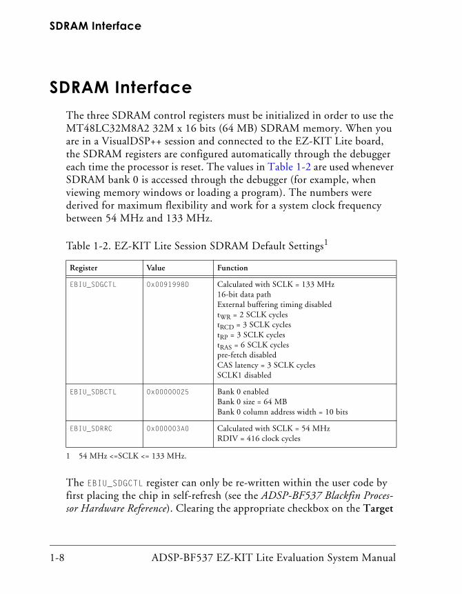
SDRAM InterfaceThe three SDRAM control registers must be initialized in order to use the MT48LC32M8A2 32M x 16 bits (64 MB) SDRAM memory. When you are in a VisualDSP++ session and connected to the EZ-KIT Lite board, the SDRAM registers are configured automatically through the debugger each time the processor is reset. The values in Table 1-2 are used whenever SDRAM bank 0 is accessed through the debugger (for example, when viewing memory windows or loading a program). The numbers were derived for maximum flexibility and work for a system clock frequency between 54 MHz and 133 MHz.
The EBIU_SDGCTL register can only be re-written within the user code by first placing the chip in self-refresh (see the ADSP-BF537 Blackfin Proces-sor Hardware Reference). Clearing the appropriate checkbox on the Target
Table 1-2. EZ-KIT Lite Session SDRAM Default Settings1
1 54 MHz <=SCLK <= 133 MHz.
Register Value Function
EBIU_SDGCTL 0x0091998D Calculated with SCLK = 133 MHz16-bit data pathExternal buffering timing disabledtWR = 2 SCLK cyclestRCD = 3 SCLK cyclestRP = 3 SCLK cyclestRAS = 6 SCLK cyclespre-fetch disabledCAS latency = 3 SCLK cyclesSCLK1 disabled
EBIU_SDBCTL 0x00000025 Bank 0 enabledBank 0 size = 64 MBBank 0 column address width = 10 bits
EBIU_SDRRC 0x000003A0 Calculated with SCLK = 54 MHzRDIV = 416 clock cycles
1-8 ADSP-BF537 EZ-KIT Lite Evaluation System Manual
Using EZ-KIT Lite
Options dialog box, which is accessible through the Settings pull-down menu, disables automatic and allows manual configuration. For more information, see online Help.
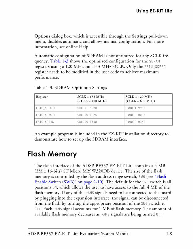
Automatic configuration of SDRAM is not optimized for any SCLK fre-quency. Table 1-3 shows the optimized configuration for the SDRAM registers using a 120 MHz and 133 MHz SCLK. Only the EBIU_SDRRC register needs to be modified in the user code to achieve maximum performance.
An example program is included in the EZ-KIT installation directory to demonstrate how to set up the SDRAM interface.
Flash MemoryThe flash interface of the ADSP-BF537 EZ-KIT Lite contains a 4 MB (2M x 16-bits) ST Micro M29W320DB device. The size of the flash memory is controlled by the flash address range switch, SW6 (see “Flash Enable Switch (SW6)” on page 2-10). The default for the SW6 switch is all positions ON, which allows the user to have access to the full 4 MB of the flash memory. If any of the ~AMS signals need to be connected to the board by plugging into the expansion interface, the signal can be disconnected from the flash by turning the appropriate position of the SW6 switch to OFF. Each ~AMS signal accounts for 1 MB of flash memory. The amount of available flash memory decreases as ~AMS signals are being turned OFF.
Table 1-3. SDRAM Optimum Settings
Register SCLK = 133 MHz(CCLK = 400 MHz)
SCLK = 120 MHz(CCLK = 600 MHz)
EBIU_SDGCTL 0x0091 998D 0x0091 998D
EBIU_SDBCTL 0x0000 0025 0x0000 0025
EBIU_SDRRC 0x0000 0408 0x0000 03A0
ADSP-BF537 EZ-KIT Lite Evaluation System Manual 1-9
CAN Interface
The last sector in the flash memory (0x1F8000–0x1FFFFF) is reserved for the Media Access Control address, which can be found on the back of the board. Each board has a unique MAC address. The sector is protected and is not erased even when the entire flash erase command is issued.
Example code is provided in the EZ-KIT Lite installation directory to demonstrate how to program the flash memory.
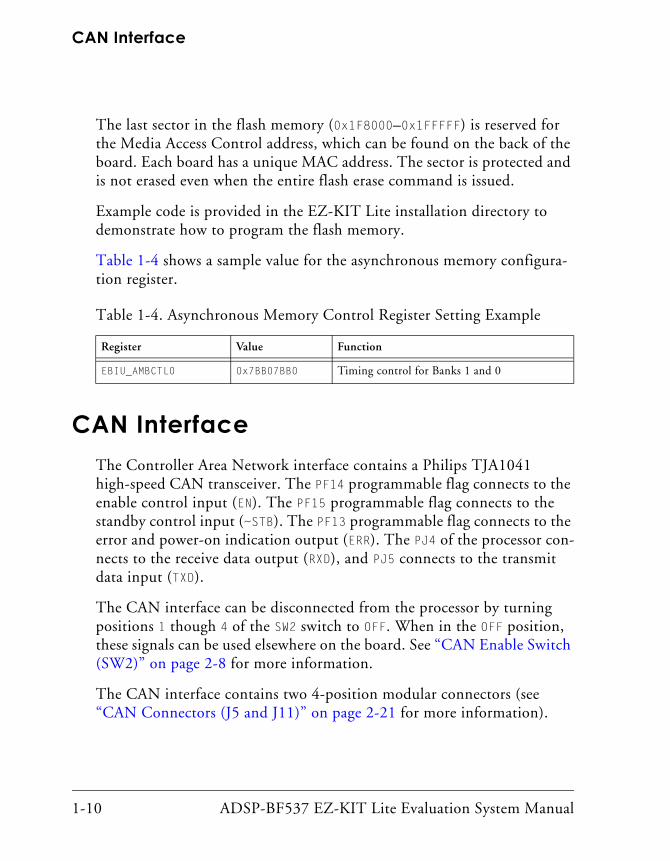
Table 1-4 shows a sample value for the asynchronous memory configura-tion register.
CAN InterfaceThe Controller Area Network interface contains a Philips TJA1041 high-speed CAN transceiver. The PF14 programmable flag connects to the enable control input (EN). The PF15 programmable flag connects to the standby control input (~STB). The PF13 programmable flag connects to the error and power-on indication output (ERR). The PJ4 of the processor con-nects to the receive data output (RXD), and PJ5 connects to the transmit data input (TXD).
The CAN interface can be disconnected from the processor by turning positions 1 though 4 of the SW2 switch to OFF. When in the OFF position, these signals can be used elsewhere on the board. See “CAN Enable Switch (SW2)” on page 2-8 for more information.
The CAN interface contains two 4-position modular connectors (see “CAN Connectors (J5 and J11)” on page 2-21 for more information).
Table 1-4. Asynchronous Memory Control Register Setting Example
Register Value Function
EBIU_AMBCTL0 0x7BB07BB0 Timing control for Banks 1 and 0
1-10 ADSP-BF537 EZ-KIT Lite Evaluation System Manual

Using EZ-KIT Lite
Example programs are included in the EZ-KIT installation directory to demonstrate the CAN circuit operation.
Ethernet InterfaceThe ADSP-BF537 processor is able to directly connect to a network with the help of an embedded Fast Ethernet MAC. The MAC supports both 10-BaseT (10 Mbits/sec) and 100-BaseT (100 Mbits/sec) operations. The 10/100 Ethernet MAC peripheral of the ADSP-BF537 processor is fully compliant with the IEEE 802.3-2002 standard and provides programma-ble features designed to minimize supervision, bus utilization, or message processing by the rest of the processor system.
The Ethernet interface contains a SMSC LAN83C185 device. The LAN83C185 is a low-power highly-integrated analog interface IC for high-performance embedded Ethernet applications.
The Ethernet connector, J4, is a RJ45 type connector with built-in mag-netics and LEDs (see “Ethernet Connector (J4)” on page 2-21).
802.3af Power-over-Ethernet (PoE) is supported when the EZ-KIT Lite connects to a Blackfin USB-LAN EZ-Extender.
Example programs are included in the EZ-KIT installation directory to demonstrate the Ethernet circuit operation.
ELVIS InterfaceThe ADSP-BF537 EZ-KIT Lite board contains the National Instruments ELVIS interface. The interface features the DC voltage and current mea-surement modules, oscilloscope and bode analyzer modules, function generator, arbitrary waveform generator, and digital IO.
ADSP-BF537 EZ-KIT Lite Evaluation System Manual 1-11

Audio Interface
The ELVIS interface is a LabVIEW-based design and prototype environ-ment for university science and engineering laboratories. The ELVIS interface consists of LabVIEW-based virtual instruments, a multifunction data acquisition (DAQ) device, and a custom-designed bench-top work-station and prototype board. This combination provides a ready-to-use suite of instruments found in most educational laboratories. Because the interface is based on LabVIEW and provides complete data acquisition and prototyping capabilities, the system is ideal for academic coursework that range from lower-division classes to advanced project-based curriculums.
For more information on ELVIS and example demonstration programs, visit National Instruments Web site at www.ni.com.
Audio InterfaceThe audio circuit consists of an AD1871 analog-to-digital converter (ADC) and an AD1854 digital-to-analog converter (DAC). The audio cir-cuit provides one channel of stereo input and one channel of stereo output via 3.5 mm stereo jacks. The SPORT0 interface of the processor is linked with the stereo audio data input and output pins of the audio circuit.
The frame sync and bit clocks are generated from the ADC and feed to the processor because the ADC is operating in master mode. The audio inter-face samples data at a 48 kHz sample rate. The serial data interface operates in Two Wire Interface mode and connects to SPORT0 of the processor.
The audio interface can be disconnected from SPORT0 by turning positions 1 and 5 of the SW7 switch OFF. When in the OFF position, the SPORT0 signals can be used on the SPORT0 connector (P6) or the expansion interface (see “SPORT0 Connector (P6)” on page 2-24 and“Audio Enable Switch (SW7)” on page 2-11 for more information).
1-12 ADSP-BF537 EZ-KIT Lite Evaluation System Manual
Using EZ-KIT Lite
Example programs are included in the EZ-KIT installation directory to demonstrate the audio circuit operation.
LEDs and Push ButtonsThe EZ-KIT Lite provides four push buttons and six LEDs for gen-eral-purpose IO.
The six LEDs, labeled LED1 through LED6, are accessed via the PF11–6 pro-cessor pins. For information on how to program the pins, refer to the ADSP-BF537 Blackfin Processor Hardware Reference.
The four general-purpose push button are labeled SW10 through SW13. A status of each individual button can be read through programmable flag (PF) inputs, PF5 through PF2. A PF reads “1” when a corresponding switch is being pressed-on. When the switch is released, the PF reads “0”. A con-nection between the push button and PF input is established through the SW5 DIP switch. See “LEDs and Push Buttons” on page 2-17 for details.
An example program is included in the EZ-KIT installation directory to demonstrate the functionality of the LEDs and push buttons.
Example ProgramsExample programs are provided with the ADSP-BF537 EZ-KIT Lite to demonstrate various capabilities of the evaluation board. These programs are installed with the EZ-KIT Lite software and can be found in the …\Blackfin\EZ-KITs\ADSP-BF537\Examples subdirectory of the Visu-alDSP++ installation directory. Please refer to the readme file provided with each example for more information.
ADSP-BF537 EZ-KIT Lite Evaluation System Manual 1-13
Background Telemetry Channel
Background Telemetry ChannelThe ADSP-BF537 USB debug agent supports the BTC, which facilitates data exchange between VisualDSP++ and the processor without interrupt-ing processor execution.
The BTC allows the user to view a variable as it is updated or changed, all while the processor continues to execute. For increased performance of the BTC, including faster reading and writing, please check out our latest line of processor emulators on the web at http://www.analog.com/proces-sors/resources/crosscore/emulators/index.html. For more information about the background telemetry channel, see the Visu-alDSP++ User’s Guide or online Help.
1-14 ADSP-BF537 EZ-KIT Lite Evaluation System Manual

2 EZ-KIT LITE HARDWARE REFERENCE
This chapter describes the hardware design of the ADSP-BF537 EZ-KIT
Lite board. The following topics are covered.• “System Architecture” on page 2-2Describes the configuration of the ADSP-BF537 EZ-KIT Lite board and explains how the board components interface with the processor.
• “Jumper and Switch Settings” on page 2-8Shows the location and describes the function of the configuration jumpers and switches.
• “LEDs and Push Buttons” on page 2-17Shows the location and describes the function of the LEDs and push buttons.
• “Connectors” on page 2-20Shows the location and gives the part number for all of the connec-tors on the board. Also, the manufacturer and part number information is given for the mating parts.
ADSP-BF537 EZ-KIT Lite Evaluation System Manual 2-1

System Architecture
System ArchitectureThis section describes the processor’s configuration on the EZ-KIT Lite board.
The EZ-KIT Lite is designed to demonstrate the capabilities of the ADSP-BF537 Blackfin processor. The processor has IO voltage of 3.3V. The core voltage of the processor is supplied by the internal voltage regulator.
Figure 2-1. System Architecture
2-2 ADSP-BF537 EZ-KIT Lite Evaluation System Manual
EZ-KIT Lite Hardware Reference
The core voltage and the core clock rate can be set on the fly by the pro-cessor. The input clock is 25 MHz. A 32.768 kHz crystal supplies the Real Time Clock (RTC) inputs of the processor. The default boot mode for the processor is flash boot. See “Boot Mode Select Switch (SW16)” on page 2-12 for information about changing the default boot mode.
External Bus Interface UnitThe external bus interface unit (EBIU) connects external memory to the ADSP-BF537 processor. The unit includes a 16-bit wide data bus, an address bus, and a control bus. On the EZ-KIT Lite, the EBIU connects to the SDRAM, flash, and expansion interfaces.
64 Mbytes (32M x 16 bits) of SDRAM connect to the synchronous mem-ory select 0 pin (~SMS0). Refer to “SDRAM Interface” on page 1-8 for information about configuring the SDRAM. Note that SDRAM clock is the processor’s clock out (CLK OUT), which must not exceed 133 MHz.
The flash memory device connects to the asynchronous memory select sig-nals, ~AMS3 through ~AMS0. The device provides a total of 4 Mbytes of flash memory. The processor can use this memory for both booting and storing information during normal operation. Refer to “Flash Memory” on page 1-9 for details.
All of the address, data, and control signals are available externally via the expansion interface (J1–3). The pinout of these connectors can be found in Appendix B, “Schematics” on page B-1.
SPORT0 Audio InterfaceThe SPORT0 interface connects to the audio circuit, the SPORT0 connector (P6), and the expansion interface. The audio circuit uses the primary data transmit and receive pins to input and output data from the audio input and outputs.
ADSP-BF537 EZ-KIT Lite Evaluation System Manual 2-3
System Architecture
The pinout of the SPORT connector and the expansion interface connectors can be found in Appendix B, “Schematics” on page B-1.
SPI InterfaceThe processor’s serial peripheral interconnect (SPI) interface is connected to the SPI connector (P9) and the expansion interface.
Programmable Flags (PFs)
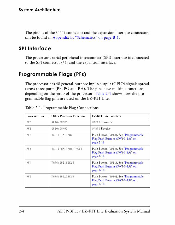
The processor has 48 general-purpose input/output (GPIO) signals spread across three ports (PF, PG and PH). The pins have multiple functions, depending on the setup of the processor. Table 2-1 shows how the pro-grammable flag pins are used on the EZ-KIT Lite.
Table 2-1. Programmable Flag Connections
Processor Pin Other Processor Function EZ-KIT Lite Function
PF0 GPIO/DMAR0 UART0 Transmit
PF1 GPIO/DMAR1 UART0 Receive
PF2 UART1_TX/TMR7 Push button (SW13). See “Programmable Flag Push Buttons (SW10–13)” on page 2-18.
PF3 UART1_RX/TMR6/TACI6 Push button (SW12). See “Programmable Flag Push Buttons (SW10–13)” on page 2-18.
PF4 TMR5/SPI_SSEL6 Push button (SW11). See “Programmable Flag Push Buttons (SW10–13)” on page 2-18.
PF5 TMR4/SPI_SSEL5 Push button (SW10). See “Programmable Flag Push Buttons (SW10–13)” on page 2-18.
2-4 ADSP-BF537 EZ-KIT Lite Evaluation System Manual

EZ-KIT Lite Hardware Reference
PF6 TMR3/SPI_SSEL4 LED (LED1). See “LEDs and Push Buttons” on page 1-13 and “Push Button Enable Switch (SW5)” on page 2-10 for informa-tion on how to disable the push button.
PF7 TMR2/PPI_FS3 LED (LED2). See “LEDs and Push Buttons” on page 1-13 and “Push Button Enable Switch (SW5)” on page 2-10 for informa-tion on how to disable the push button.
PF8 TMR1/PPI_FS2 LED (LED3). See “LEDs and Push Buttons” on page 1-13 and “Push Button Enable Switch (SW5)” on page 2-10 for informa-tion on how to disable the push button.
PF9 TMR0/PPI_FS1 LED (LED4). See “LEDs and Push Buttons” on page 1-13 for information on how to dis-able the push button.
PF10 SPI_SSEL1 LED (LED5). See “LEDs and Push Buttons” on page 1-13 for information on how to dis-able the push button.
PF11 SPI_MOSI LED (LED6). See “LEDs and Push Buttons” on page 1-13 for information on how to dis-able the push button.
PF12 SPI_MISO Audio Reset
PF13 SPI_SCK CAN ERR
PF14 SPI_SS/TACLK0 CAN EN
PF15 PPI4_CLK/TMRCLK CAN STB
PG0 PPI_D0 ELVIS_TRIGGER
PG1 PPI_D1 ELVIS_PF1
PG2 PPI_D2 ELVIS_PF2
PG3 PPI_D3 ELVIS_PF5
PG4 PPI_D4 ELVIS_PF6
Table 2-1. Programmable Flag Connections (Cont’d)
Processor Pin Other Processor Function EZ-KIT Lite Function
ADSP-BF537 EZ-KIT Lite Evaluation System Manual 2-5

System Architecture
PG5 PPI_D5 ELVIS_PF7
PG6 PPI_D6 UART0_CTS
PG7 PPI_D7 UART0_RTS
PG8 PPI_D8/DR1SEC Not used
PG9 PPI_D9/DT1SEC Not used
PG10 PPI_D10/RSCLK1 Not used
PG11 PPI_D11/RFS1 Not used
PG12 PPI_D12/DR1PRI Not used
PG13 PPI_D13/TSCLK1 Not used
PG14 PPI_D14/TFS1 No used
PG15 PPI_D15/DT1PRI USB_IRQ used for USB bus power
PH0 ETXD0 ETXD used for Ethernet interface
PH1 ETXD1 ETXD1 used for Ethernet interface
PH2 ETXD2 ETXD2 used for Ethernet interface
PH3 ETXD3 ETXD3 used for Ethernet interface
PH4 ETXEN ETXEN used for Ethernet interface
PH5 MII_TXCLK/RMII_REF_CLK MII_TXCLK used for Ethernet interface
PH6 MII_PHYINT/RMII_MDINT Not used
PH7 COL COL used for Ethernet interface
PH8 ERXD0 ERXD0 used for Ethernet interface
PH9 ERXD1 ERXD1 used for Ethernet interface
PH10 ERXD2 ERXD2 used for Ethernet interface
PH11 ERXD3 ERXD3 used for Ethernet interface
PH12 ERXDV/TACLK5 ERXDV used for Ethernet interface
Table 2-1. Programmable Flag Connections (Cont’d)
Processor Pin Other Processor Function EZ-KIT Lite Function
2-6 ADSP-BF537 EZ-KIT Lite Evaluation System Manual

EZ-KIT Lite Hardware Reference
UART PortThe processor’s universal asynchronous receiver/transmitter (UART) port connects to the ADM3202 RS-232 line driver as well as to the expansion interface. The RS-232 line driver connects to the DB9 female connector, providing an interface to a PC or other serial device.
Expansion InterfaceThe expansion interface consists of three 90-pin connectors. Table 2-2 shows the interfaces each connector provides. For the exact pinout of these connectors, refer to Appendix B, “Schematics” on page B-1. The mechan-ical dimensions of the connectors can be obtained from Technical or Customer Support.
Analog Devices offers many EZ-Extender products that plug on to the expansion interface. For more information on these products, visit the Analog Devices Web site at www.analog.com.
PH13 ERXCLK/TACLK6 ERXCLK used for Ethernet interface
PH14 ERXER/TACLK7 ERXER used for Ethernet interface
PH15 MII_CRS/RMII_CRS_DV MII_CRS used for Ethernet interface
Table 2-2. Expansion Interface Connectors
Connector Interfaces
J1 5V, G ND, address, data, PPI
J2 3.3V, GND, SPI, NMI, TMR2–0, SPORT0, SPORT1, PF15–0, EBUI control signals
J3 5V, 3.3V, GND, UART, flash IO, reset, video control signals
Table 2-1. Programmable Flag Connections (Cont’d)
Processor Pin Other Processor Function EZ-KIT Lite Function
ADSP-BF537 EZ-KIT Lite Evaluation System Manual 2-7

Jumper and Switch Settings
Limits to the current and to the interface speed must be taken into consid-eration when using the expansion interface. The maximum current limit is dependent on the capabilities of the regulator used. Additional circuitry can also add extra loading to signals, decreasing their maximum effective speed.
Analog Devices does not support and is not responsible for the effects of additional circuitry.
JTAG Emulation PortThe JTAG emulation port allows an emulator to access the processor’s internal and external memory through a 6-pin interface. The JTAG emu-lation port of the processor connects also to the USB debugging interface. When an emulator connects to the board at P4, the USB debugging inter-face is disabled. See “JTAG Connector (P4)” on page 2-23 for more information about the connector.
To learn more about available emulators, contact Analog Devices (see “Processor Product Information”).
Jumper and Switch SettingsThis section describes the operation of the jumpers and switches. The jumpers and switch locations are shown in Figure 1-1 on page 1-4.
CAN Enable Switch (SW2)The Controller Area Network (CAN) enable switch (SW2) disconnects the CAN signals from the GPIO pins of the processor. When the SW2 switch is in the OFF position, the associated GPIO signal (see Table 2-3) can be used on the expansion interface.
2-8 ADSP-BF537 EZ-KIT Lite Evaluation System Manual

EZ-KIT Lite Hardware Reference
Ethernet Mode Select Switch (SW3)The Ethernet mode select switch (SW3) controls the configuration of the 10/100 digital block in the LAN83C185 PHY device (see Table 2-4).
UART Enable Switch (SW4)The UART enable switch (SW4) disconnects UART signals from the GPIO pins of the processor. When the switch is in the OFF position, the associ-ated GPIO signal (see Table 2-5) can be used on the expansion interface.
Table 2-3. CAN Enable Switch (SW2)
CAN Signal SW2 Switch Position (Default) Processor Signal
ENABLE 1 (ON) PF14
STANDBY 2 (ON) PF15
ERROR 3 (ON) PF13
RECEIVE DATA 4 (ON) PJ4
Table 2-4. Ethernet Mode Select Switch (SW3)
SW3 Switch Position Ethernet Mode
3 2 1
ON ON ON 10Base-T half duplex; auto-negotiation disabled
ON ON OFF 10Base-T full duplex; auto-negotiation disabled
ON OFF ON 100Base-T half duplex; auto-negotiation disabled
ON OFF OFF 100Base-T full duplex; auto-negotiation disabled
OFF ON ON 100Base-T half duplex; auto-negotiation enabled
OFF ON OFF Repeater mode; auto-negotiation enabled
OFF OFF ON Power down mode
OFF OFF OFF All capable; auto-negotiation enabled (default)
ADSP-BF537 EZ-KIT Lite Evaluation System Manual 2-9
Jumper and Switch Settings
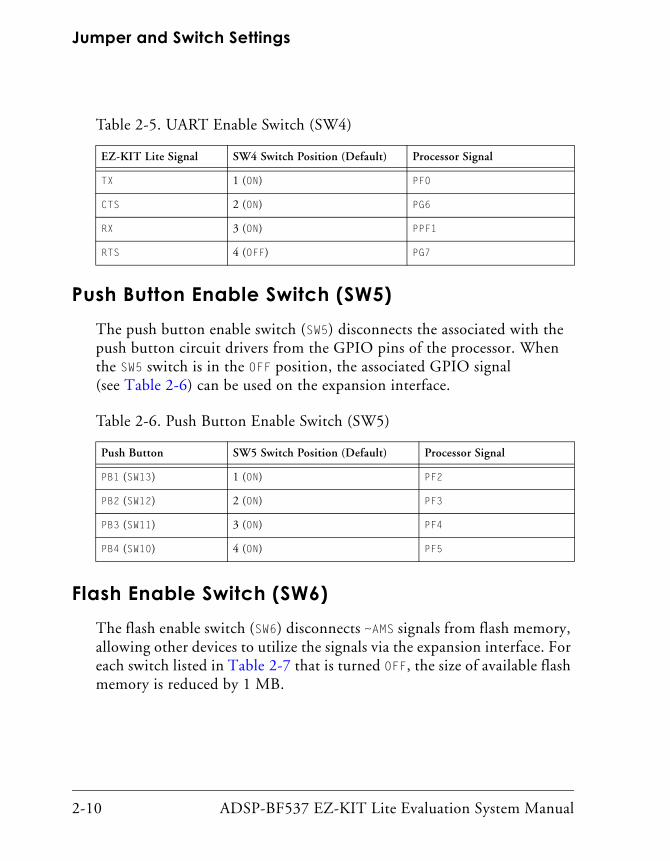
Push Button Enable Switch (SW5)The push button enable switch (SW5) disconnects the associated with the push button circuit drivers from the GPIO pins of the processor. When the SW5 switch is in the OFF position, the associated GPIO signal (see Table 2-6) can be used on the expansion interface.
Flash Enable Switch (SW6)The flash enable switch (SW6) disconnects ~AMS signals from flash memory, allowing other devices to utilize the signals via the expansion interface. For each switch listed in Table 2-7 that is turned OFF, the size of available flash memory is reduced by 1 MB.
Table 2-5. UART Enable Switch (SW4)
EZ-KIT Lite Signal SW4 Switch Position (Default) Processor Signal
TX 1 (ON) PF0
CTS 2 (ON) PG6
RX 3 (ON) PPF1
RTS 4 (OFF) PG7
Table 2-6. Push Button Enable Switch (SW5)
Push Button SW5 Switch Position (Default) Processor Signal
PB1 (SW13) 1 (ON) PF2
PB2 (SW12) 2 (ON) PF3
PB3 (SW11) 3 (ON) PF4
PB4 (SW10) 4 (ON) PF5
2-10 ADSP-BF537 EZ-KIT Lite Evaluation System Manual
EZ-KIT Lite Hardware Reference
Audio Enable Switch (SW7) The audio enable switch (SW7) disconnects the audio signals from the pro-cessor (positions 1–5) and determines how the clock for the audio circuit generates and connects (positions 6–8). Position 8 determines if the ADC is in master or slave mode. When in master mode (position 8 is ON), the ADC generates the clock. When in slave mode (position 8 is OFF), the pro-cessor generates the clock. Positions 6 and 7 connect the transmit and receive clocks together (see Table 2-8).
Table 2-7. Flash Enable Switch (SW6)
Processor Signal SW6 Switch Position (Default)
~AMS0 1 (ON)
~AMS1 2 (ON)
~AMS2 3 (ON)
~AMS3 4 (ON)
Table 2-8. Audio Enable Switch (SW7)
EZ-KIT Lite Signal SW7 Switch Position (Default) Processor Signal
DR0PRI 1 (ON) PJ8
RSCLK0 2 (ON) PJ6
RFS0 3 (ON) PJ7
TSCLK0 4 (ON) PG9
TFS0 5 (ON) PJ10
Clock Loopback 6 (ON)
FS Loopback 7 (ON)
ADC Master/Slave 8 (ON)
ADSP-BF537 EZ-KIT Lite Evaluation System Manual 2-11

Jumper and Switch Settings
Boot Mode Select Switch (SW16)The rotary switch (SW16) determines the boot mode of the processor. Table 2-9 shows the available boot mode settings. By default, the ADSP-BF537 processor boots from the on-board flash memory.
3V Power Selection Jumper (JP3)The 3V power selection jumper (JP3) selects the power source for the 3-volt parts. In a standard mode of operation, the parts are powered by the on-board switching regulator circuit (ADP3025) via an external power sup-ply. When a Blackfin USB-LAN EZ-Extender connects to the EZ-KIT Lite, power can be derived from the USB bus power or Power-over-Ether-net (802.3af). In this case, the board can operate without an external power supply. The jumper settings are shown in Table 2-10.
Table 2-9. Boot Mode Select Switch (SW16)
SW16 Position Processor Boot Mode
0 Execute from 16-bit external memory
1 Boot from 16-bit flash memory (default)
2 Reserved
3 Boot from SPI memory
4 Boot from SPI host
5 Boot from Serial TWI memory
6 Boot from TWI host
7 Boot from UART host
2-12 ADSP-BF537 EZ-KIT Lite Evaluation System Manual
EZ-KIT Lite Hardware Reference
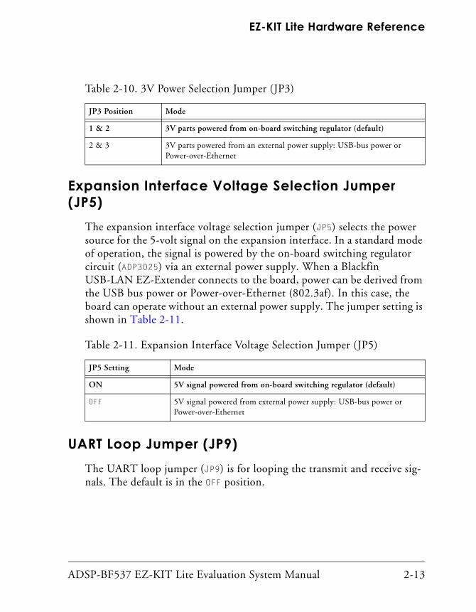
Expansion Interface Voltage Selection Jumper (JP5)
The expansion interface voltage selection jumper (JP5) selects the power source for the 5-volt signal on the expansion interface. In a standard mode of operation, the signal is powered by the on-board switching regulator circuit (ADP3025) via an external power supply. When a Blackfin USB-LAN EZ-Extender connects to the board, power can be derived from the USB bus power or Power-over-Ethernet (802.3af). In this case, the board can operate without an external power supply. The jumper setting is shown in Table 2-11.
UART Loop Jumper (JP9)The UART loop jumper (JP9) is for looping the transmit and receive sig-nals. The default is in the OFF position.
Table 2-10. 3V Power Selection Jumper (JP3)
JP3 Position Mode
1 & 2 3V parts powered from on-board switching regulator (default)
2 & 3 3V parts powered from an external power supply: USB-bus power or Power-over-Ethernet
Table 2-11. Expansion Interface Voltage Selection Jumper (JP5)
JP5 Setting Mode
ON 5V signal powered from on-board switching regulator (default)
OFF 5V signal powered from external power supply: USB-bus power or Power-over-Ethernet
ADSP-BF537 EZ-KIT Lite Evaluation System Manual 2-13
Jumper and Switch Settings
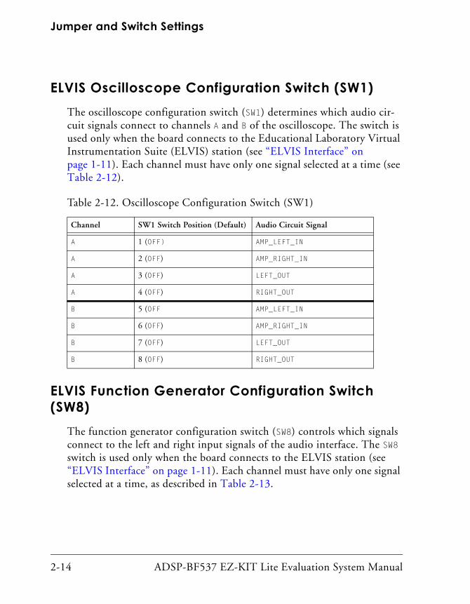
ELVIS Oscilloscope Configuration Switch (SW1)The oscilloscope configuration switch (SW1) determines which audio cir-cuit signals connect to channels A and B of the oscilloscope. The switch is used only when the board connects to the Educational Laboratory Virtual Instrumentation Suite (ELVIS) station (see “ELVIS Interface” on page 1-11). Each channel must have only one signal selected at a time (see Table 2-12).
ELVIS Function Generator Configuration Switch (SW8)
The function generator configuration switch (SW8) controls which signals connect to the left and right input signals of the audio interface. The SW8 switch is used only when the board connects to the ELVIS station (see “ELVIS Interface” on page 1-11). Each channel must have only one signal selected at a time, as described in Table 2-13.
Table 2-12. Oscilloscope Configuration Switch (SW1)
Channel SW1 Switch Position (Default) Audio Circuit Signal
A 1 (OFF) AMP_LEFT_IN
A 2 (OFF) AMP_RIGHT_IN
A 3 (OFF) LEFT_OUT
A 4 (OFF) RIGHT_OUT
B 5 (OFF AMP_LEFT_IN
B 6 (OFF) AMP_RIGHT_IN
B 7 (OFF) LEFT_OUT
B 8 (OFF) RIGHT_OUT
2-14 ADSP-BF537 EZ-KIT Lite Evaluation System Manual

EZ-KIT Lite Hardware Reference
ELVIS Voltage Selection Jumper (JP6)The ELVIS voltage selection jumper (JP6) is used to select the power source for the EZ-KIT Lite. In a standard mode of operation, the board receives its power from an external power supply. When JP6 is installed, the board is powered from an ELVIS station and no external power supply is required. The jumper setting is shown in Table 2-14.
The external power supply must be disconnected from the board when JP6 is installed. In this case, the power supply may cause damage to the EZ-KIT Lite board and ELVIS unit.
Table 2-13. Function Generator Configuration Switch (SW8)
Channel SW8 Switch Position (Default) Audio Signal
AMP_LEFT_IN 1 (ON) LEFT_IN
AMP_RIGHT_IN 2 (ON) RIGHT_IN
AMP_LEFT_IN 3 (OFF) DAC0
AMP_RIGHT_IN 4 (OFF) DAC1
AMP_LEFT_IN 5 (OFF) FUNCT_OUT
AMP_RIGHT_IN 6 (OFF) FUNCT_OUT
Table 2-14. ELVIS Voltage Selection Jumper (JP6)
JP6 Setting Mode
OFF Powered from an external power supply (default)
ON Powered from ELVIS
ADSP-BF537 EZ-KIT Lite Evaluation System Manual 2-15

Jumper and Switch Settings
ELVIS Select Jumper (JP8)The ELVIS select jumper (JP8) configures the EZ-KIT Lite’s connection to an ELVIS station (see “ELVIS Interface” on page 1-11). When JP8 is installed, the connections to the push buttons and LED are re-directed to the ELVIS station, instead of the processor. The jumper setting is shown in Table 2-15.
Table 2-15. ELVIS Select Jumper (JP8)
JP8 Setting Mode
OFF Not connected to ELVIS (default)
ON Connected to ELVIS
2-16 ADSP-BF537 EZ-KIT Lite Evaluation System Manual

EZ-KIT Lite Hardware Reference
LEDs and Push ButtonsThis section describes the functionality of the LEDs and push buttons. Figure 2-2 shows the locations of the LEDs and push buttons.
Reset Push Button (SW9)The RESET push button resets all of the ICs on the board. One exception is the USB interface chip. The chip is not being reset when the push button is pressed after the USB cable has been plugged in and communication has been correctly initialized with the PC. After USB communication has been initialized, the only way to reset the USB is by powering down the board.
Figure 2-2. LED and Push Button Locations
ADSP-BF537 EZ-KIT Lite Evaluation System Manual 2-17
LEDs and Push Buttons
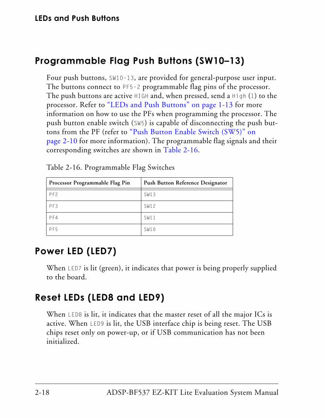
Programmable Flag Push Buttons (SW10–13)Four push buttons, SW10–13, are provided for general-purpose user input. The buttons connect to PF5–2 programmable flag pins of the processor. The push buttons are active HIGH and, when pressed, send a High (1) to the processor. Refer to “LEDs and Push Buttons” on page 1-13 for more information on how to use the PFs when programming the processor. The push button enable switch (SW5) is capable of disconnecting the push but-tons from the PF (refer to “Push Button Enable Switch (SW5)” on page 2-10 for more information). The programmable flag signals and their corresponding switches are shown in Table 2-16.
Power LED (LED7)When LED7 is lit (green), it indicates that power is being properly supplied to the board.
Reset LEDs (LED8 and LED9)When LED8 is lit, it indicates that the master reset of all the major ICs is active. When LED9 is lit, the USB interface chip is being reset. The USB chips reset only on power-up, or if USB communication has not been initialized.
Table 2-16. Programmable Flag Switches
Processor Programmable Flag Pin Push Button Reference Designator
PF2 SW13
PF3 SW12
PF4 SW11
PF5 SW10
2-18 ADSP-BF537 EZ-KIT Lite Evaluation System Manual

EZ-KIT Lite Hardware Reference
User LEDs (LED1–6)Six LEDs connect to six general-purpose IO pins of the processor (see Table 2-17)). The LEDs are active HIGH and are lit by writing a “1” to the correct PF signal. Refer to “LEDs and Push Buttons” on page 1-13 for more information about how to use the flash when programming the LEDs.
USB Monitor LED (LED10)The USB Monitor LED (LED10) indicates that USB communication has been initialized successfully, and you can connect to the processor using a VisualDSP++ EZ-KIT Lite session. This should take approximately 15 seconds. If the LED does not light, try cycling power on the board and/or reinstalling the USB driver (see the VisualDSP++ Installation Quick Refer-ence Card).
When VisualDSP++ is actively communicating with the EZ-KIT Lite target board, the LED can flicker, indicating communications handshake.
Table 2-17. User LEDs
LED Reference Designator Processor Programmable Flag Pin
LED1 PF6
LED2 PF7
LED3 PF8
LED4 PF9
LED5 PF10
LED6 PF11
ADSP-BF537 EZ-KIT Lite Evaluation System Manual 2-19
Connectors
ConnectorsThis section describes the connector functionality and provides informa-tion about mating connectors. The locations of the connectors are shown in Figure 2-3.
Figure 2-3. Connector Locations
2-20 ADSP-BF537 EZ-KIT Lite Evaluation System Manual

EZ-KIT Lite Hardware Reference
Audio Connectors (J9 and J10)
CAN Connectors (J5 and J11)
Ethernet Connector (J4)
Part Description Manufacturer Part Number
3.5 mm stereo jack A/D Electronics ST323-5
Mating Cable (shipped with EZ-KIT Lite)
3.5 mm stereo interconnect cable
Random 0A3-01106
3.5 mm headphones Koss UR5
Part Description Manufacturer Part Number
Modular Jack AMP 558872-1
Mating Cable
4 conductor modular jack cable L-COM TSP3044
Part Description Manufacturer Part Number
Ethernet Jack Pulse JK0-0025
Mating Cable (shipped with EZ-KIT Lite)
Cat 5E patch cable Random PC10/100T-007
Cat 5E crossover cable Random PC10/100TC-007
ADSP-BF537 EZ-KIT Lite Evaluation System Manual 2-21
Connectors
RS-232 Connector (J6)
Power Connector (J7)The power connector provides all of the power necessary to operate the EZ-KIT Lite board.
The power connector supplies DC power to the EZ-KIT Lite board. Table 2-18 shows the power supply specifications.
Part Description Manufacturer Part Number
DB9, Female, Vertical Mount Digi-Key 191-009-213-571-ND
Mating Cable
2m Female to female cable Digi-Key AE1020-ND
Part Description Manufacturer Part Number
2.5 mm Power Jack SWITCHCRAFT RAPC712
Mating Power Supply (shipped with EZ-KIT Lite)
7V Power Supply CUI Inc. DMS070214-P6P-SZ
Table 2-18. Power Supply Specification
Terminal Connection
Center pin +7 [email protected] amps
Outer Ring GND
2-22 ADSP-BF537 EZ-KIT Lite Evaluation System Manual

EZ-KIT Lite Hardware Reference
Expansion Interface Connectors (J1–3)Three board-to-board connector footprints provide signals for most of the processor’s peripheral interfaces. The connectors are located at the bottom of the board. For more information about the expansion interface, see “Expansion Interface” on page 2-7. For the availability and pricing of the J1, J12, and J3 connectors, contact Samtec.
JTAG Connector (P4)The JTAG header is the connecting point for a JTAG in-circuit emulator pod. When an emulator connects to the JTAG header, the USB debug interface is disabled.
Pin 3 is missing to provide keying. Pin 3 in the mating connector should have a plug.
When using an emulator with the EZ-KIT Lite board, follow the connection instructions provided with the emulator.
Part Description Manufacturer Part Number
90 Position 0.05" Spacing, SMT
Samtec SFC-145-T2-F-D-A
Mating Connector
90 Position 0.05” Spacing (Through Hole)
Samtec TFM-145-x1 Series
90 Position 0.05” Spacing (Surface Mount)
Samtec TFM-145-x2 Series
90 Position 0.05” Spacing (Low Cost)
Samtec TFC-145 Series
ADSP-BF537 EZ-KIT Lite Evaluation System Manual 2-23
Connectors
SPORT0 Connector (P6)The pinout for the P6 connector can be found in Appendix B, “Schemat-ics” on page B-1.
SPORT1 Connector (P7)The pinout for the P7 connector can be found in Appendix B, “Schemat-ics” on page B-1.
PPI Connector (P8)The pinout for the P8 connector can be found in Appendix B, “Schemat-ics” on page B-1.
Part Description Manufacturer Part Number
IDC Header Digi-Key S2012-17-ND
Mating Connector
IDC socket Digi-Key S4217-ND
Part Description Manufacturer Part Number
IDC Header Digi-Key S2012-17-ND
Mating Connector
IDC socket Digi-Key S4217-ND
Part Description Manufacturer Part Number
IDC Header Digi-Key S2012-20-ND
Mating Connector
IDC socket Digi-Key S4220-ND
2-24 ADSP-BF537 EZ-KIT Lite Evaluation System Manual

EZ-KIT Lite Hardware Reference
SPI Connector (P9)The pinout for the P9 connector can be found in Appendix B, “Schemat-ics” on page B-1.
Two-Wire Interface Connector (P10)The pinout for the P10 connector can be found in Appendix B, “Schemat-ics” on page B-1.
TIMERS Connector (P11)The pinout for the P11 connector can be found in Appendix B, “Schemat-ics” on page B-1.
Part Description Manufacturer Part Number
IDC Header Digi-Key S2012-10-ND
Mating Connector
IDC socket Digi-Key S4210-ND
Part Description Manufacturer Part Number
IDC Header Digi-Key S2012-10-ND
Mating Connector
IDC socket Digi-Key S4210-ND
Part Description Manufacturer Part Number
IDC Header Digi-Key S2012-05-ND
Mating Connector
IDC socket Digi-Key S4205-ND
ADSP-BF537 EZ-KIT Lite Evaluation System Manual 2-25
Connectors
UART1 Connector (P12)The pinout for the P12 connector can be found in Appendix B, “Schemat-ics” on page B-1.
Part Description Manufacturer Part Number
IDC Header Digi-Key S2012-05-ND
Mating Connector
IDC socket Digi-Key S4205-ND
2-26 ADSP-BF537 EZ-KIT Lite Evaluation System Manual
A BILL OF MATERIALS
The bill of materials corresponds to the board schematics on page B-1.
Please check the latest schematics on the Analog Devices website, http://www.analog.com/Processors/Processors/DevelopmentTools/technicalLibrary/manuals/DevToolsIndex.html#Evalua-
tion%20Kit%20Manuals.
ADSP-BF537 EZ-KIT Lite Evaluation System Manual A-1

Ref
.#
Des
crip
tion
Ref
eren
ce D
esig
nato
r M
anuf
actu
rer
Part
Num
ber
11
SN74
LVT
244D
W S
OIC
20U
46
TI
SN74
LVT
244B
DW
21
10M
HZ
SM
T O
SC00
3U
5 R
ALT
RO
NC
0431
0-10
.00
31
74LV
C14
A S
OIC
14U
37
TI
74L
VC
14A
D
41
IDT
74FC
T32
44A
PY
SSO
P20
U36
ID
TID
T74
FCT
3244
AP
Y
51
CY
7C64
603-
128
PQ
FP12
8U
10
CY
PR
ESS
CY
7C64
603-
128N
C
61
MM
BT
4401
SO
T-2
3Q
1 FA
IRC
HIL
DM
MB
T44
01
71
AD
P33
31A
RT
SO
T23
-6V
R2
AN
ALO
G
DE
VIC
ES
AD
P33
31A
RT
81
25M
HZ
SM
T O
SC00
5Y
1E
PSO
NM
A-5
05 2
5.00
0M-C
0
91
CY
7C10
19B
V33
-15V
C S
OJ3
2U
25
CY
PR
ESS
CY
7C10
19B
V33
-12V
C
101
12.0
MH
Z T
HR
OSC
006
Y4
DIG
I-K
EY
300-
6027
-ND
115
SN74
AH
C1G
00 S
OT
23-5
U39
-43
TI
SN74
AH
C1G
00D
BV
R
121
12.2
88M
HZ
SM
T O
SC00
3U
4 D
IGI-
KE
YSG
-800
2CA
-PC
C-N
D
132
GS7
4116
TSO
P44
U
8-9
GSI
TE
CH
-N
OLO
GY
GS7
4116
AT
P-1
0
141
32.7
68K
HZ
SM
T O
SC00
8Y
2E
PSO
NM
C-1
56 3
2.76
80K
A-A
0
151
XC
2S15
0E F
T25
6U
1 X
ILIN
XX
C2S
150E
-7FT
256C
161
SN74
LVC
1G32
SO
T23
-5
U52
TI
SN74
LVC
1G32
DB
VR
176
SN74
LVC
1G08
SO
T23
-5U
22,U
47-5
0,U
58
TI
SN74
LVC
1G08
DB
VR
182
MT
48LC
32M
8A2
TSO
P54
U15
-16
MIC
RO
NM
T48
LC32
M8A
2TG
-75
A-2 ADSP-BF537 EZ-KIT Lite Evaluation System Manual

Bill Of Materials
191
TJA
1041
SO
IC14
U
21
PHIL
IPS
TJA
1041
T
201
LA
N83
C18
5 T
QFP
64
U14
SM
SCL
AN
83C
185-
JD
214
SI48
20D
Y S
OIC
8U
17-2
0 V
ISH
AY
SI48
20D
Y-T
1
221
BF5
37 2
4LC
32 "
U34
"U
34
Atm
el24
LC
32
231
FDS9
431A
SO
IC8
U28
FAIR
CH
ILD
FDS9
431A
241
BF5
37 D
SM21
50F5
V "
U13
"U
13
ST M
ICR
OD
SM21
50F5
V
251
BF5
37 M
29W
320D
B "
U24
"U
24
ST M
ICR
OM
29W
320D
B70
ZA
6
261
AD
M70
8SA
R S
OIC
8U
27
AN
ALO
G
DE
VIC
ES
AD
M70
8SA
R
271
AD
P33
38A
KC
-33
SOT
-223
VR
1 A
NA
LOG
D
EV
ICE
SA
DP
3338
AK
C-3
.3
283
LM
V72
2M S
OIC
8U
29-3
1 N
AT
ION
AL
SE
MI
LM
V72
2M
291
AD
1854
JRS
SSO
P28
U38
A
NA
LOG
D
EV
ICE
SA
D18
54JR
S
301
AD
1871
YR
S SS
OP
28U
33
AN
AL
OG
D
EV
ICE
SA
D18
71Y
RS
311
AD
M32
02A
RN
SO
IC16
U32
A
NA
LOG
D
EV
ICE
SA
DM
3202
AR
N
322
AD
623
USO
IC8
U2-
3 A
NA
LOG
D
EV
ICE
SA
D62
3AR
M-R
EE
L
Ref
.#
Des
crip
tion
Ref
eren
ce D
esig
nato
r M
anuf
actu
rer
Part
Num
ber
ADSP-BF537 EZ-KIT Lite Evaluation System Manual A-3
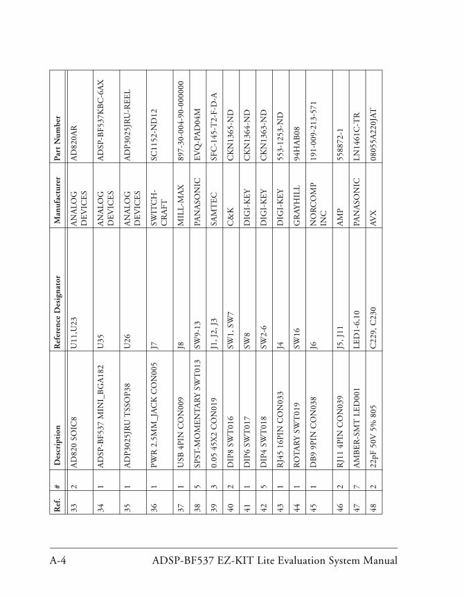
332
AD
820
SOIC
8U
11,U
23
AN
ALO
G
DE
VIC
ES
AD
820A
R
341
AD
SP-B
F537
MIN
I_B
GA
182
U35
A
NA
LOG
D
EV
ICE
SA
DSP
-BF5
37K
BC
-6A
X
351
AD
P30
25JR
U T
SSO
P38
U26
A
NA
LOG
D
EV
ICE
SA
DP
3025
JRU
-RE
EL
361
PW
R 2
.5M
M_J
AC
K C
ON
005
J7
SWIT
CH
-C
RA
FTSC
1152
-ND
12
371
USB
4PI
N C
ON
009
J8
MIL
L-M
AX
897-
30-0
04-9
0-00
0000
385
SPST
-MO
ME
NT
AR
Y S
WT
013
SW9-
13
PAN
ASO
NIC
EV
Q-P
AD
04M
393
0.05
45X
2 C
ON
019
J1, J
2, J
3 SA
MT
EC
SFC
-145
-T2-
F-D
-A
402
DIP
8 SW
T01
6SW
1, S
W7
C&
KC
KN
1365
-ND
411
DIP
6 SW
T01
7SW
8 D
IGI-
KE
YC
KN
1364
-ND
425
DIP
4 SW
T01
8SW
2-6
DIG
I-K
EY
CK
N13
63-N
D
431
RJ4
5 16
PIN
CO
N03
3J4
D
IGI-
KE
Y55
3-12
53-N
D
441
RO
TA
RY
SW
T01
9SW
16
GR
AY
HIL
L94
HA
B08
451
DB
9 9P
IN C
ON
038
J6N
OR
CO
MP
IN
C19
1-00
9-21
3-57
1
462
RJ1
1 4P
IN C
ON
039
J5, J
11A
MP
5588
72-1
477
AM
BE
R-S
MT
LE
D00
1L
ED
1-6,
10
PAN
ASO
NIC
LN
1461
C-T
R
482
22pF
50V
5%
805
C22
9, C
230
AV
X08
055A
220J
AT
Ref
.#
Des
crip
tion
Ref
eren
ce D
esig
nato
r M
anuf
actu
rer
Part
Num
ber
A-4 ADSP-BF537 EZ-KIT Lite Evaluation System Manual

Bill Of Materials
492
10uF
16V
10%
CC
T7
AN
D C
T8
SPR
AG
UE
293D
106X
9016
C2T
503
100
100M
W 5
% 8
05R
100-
101,
R10
3 A
VX
CR
21-1
01J-
T
517
600
100M
HZ
200
MA
603
FER
2-6,
FER
9 M
UR
AT
AB
LM
11A
601S
PT
521
2A S
2A_R
EC
T D
O-2
14A
AD
4 V
ISH
AY
S2A
/52
531
68U
F 6.
3V 2
0% D
CT
5 PA
NA
SON
ICE
CS-
TO
JD68
6R
541
340K
1/8
W 1
% 8
05R
166
DA
LE
CR
CW
0805
-340
3FT
551
698K
1/8
W 1
% 8
05R
167
DA
LE
CR
CW
0805
-698
3FT
562
68U
F 25
V 2
0% C
AP
003
CT
1-2
PAN
ASO
NIC
EE
V-F
C1E
680P
571
332K
1/1
0W 1
% 8
05R
164
PHIL
IPS
9C08
052A
3323
FKR
T/R
581
10U
H 4
7 +
/-20
IN
D00
1L
1 D
IGI-
KE
Y44
5-12
02-2
-ND
592
270
1/10
W 5
% 8
05R
99,R
136
PH
YC
OM
P9C
0805
2A27
00JL
HFT
605
10K
31M
W 5
% R
NE
T8
RN
1-5
CT
S74
6X10
1103
J
611
190
100M
HZ
5A
FE
R00
2FE
R7
MU
RA
TA
DLW
5BSN
191S
Q2
621
1A Z
HC
S100
0 SO
T23
DD
5 Z
ET
EX
ZH
CS1
000
632
0.47
UF
16V
10%
805
C19
9-20
0 A
VX
0805
YC
474K
AT
2A
645
1UF
10V
10%
805
C13
4,C
210,
C22
0-22
2A
VX
0805
ZC
105K
AT
2A
6519
10U
F 6.
3V 1
0% 8
05C
158,
C17
6,C
182-
184,
C20
6-20
9,C
212-
219
AV
X08
0560
106K
AT
2A
6643
0.1U
F 10
V 1
0% 4
02C
55-5
7,C
59-6
0,C
111-
114,
C13
9-14
0,C
146-
149,
C15
2-15
7,C
168-
175
,C18
5-19
8
AV
X04
02Z
D10
4KA
T2A
Ref
.#
Des
crip
tion
Ref
eren
ce D
esig
nato
r M
anuf
actu
rer
Part
Num
ber
ADSP-BF537 EZ-KIT Lite Evaluation System Manual A-5
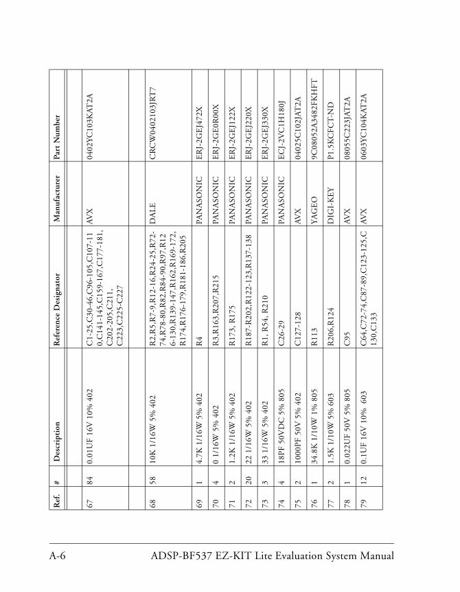
6784
0.01
UF
16V
10%
402
C
1-25
,C30
-46,
C96
-105
,C10
7-11
0,C
141-
145,
C15
9-16
7,C
177-
181,
C20
2-20
5,C
211,
C
223,
C22
5-C
227
AV
X04
02Y
C10
3KA
T2A
6858
10K
1/1
6W 5
% 4
02
R2,
R5,
R7-
9,R
12-1
6,R
24-2
5,R
72-
74,R
78-8
0,R
82,R
84-9
0,R
97,R
126-
130,
R13
9-14
7,R
162,
R16
9-17
2,R
174,
R17
6-17
9,R
181-
186,
R20
5
DA
LE
CR
CW
0402
103J
RT
7
691
4.7K
1/1
6W 5
% 4
02
R4
PAN
ASO
NIC
ER
J-2G
EJ4
72X
704
0 1/
16W
5%
402
R3,
R16
3,R
207,
R21
5PA
NA
SON
ICE
RJ-
2GE
0R00
X
712
1.2K
1/1
6W 5
% 4
02
R17
3, R
175
PAN
ASO
NIC
ER
J-2G
EJ1
22X
7220
22 1
/16W
5%
402
R18
7-R
202,
R12
2-12
3,R
137-
138
PAN
ASO
NIC
ER
J-2G
EJ2
20X
733
33 1
/16W
5%
402
R1,
R54
, R21
0PA
NA
SON
ICE
RJ-
2GE
J330
X
744
18P
F 50
VD
C 5
% 8
05
C26
-29
PAN
ASO
NIC
EC
J-2V
C1H
180J
752
1000
PF
50V
5%
402
C
127-
128
AV
X04
025C
102J
AT
2A
761
34.8
K 1
/10W
1%
805
R
113
YA
GE
O9C
0805
2A34
82FK
HFT
772
1.5K
1/1
0W 5
% 6
03
R20
6,R
124
DIG
I-K
EY
P1.
5KC
FCT
-ND
781
0.02
2UF
50V
5%
805
C
95
AV
X08
055C
223J
AT
2A
7912
0.1U
F 16
V 1
0% 6
03
C64
,C72
-74,
C87
-89,
C12
3-12
5,C
130,
C13
3A
VX
0603
YC
104K
AT
2A
Ref
.#
Des
crip
tion
Ref
eren
ce D
esig
nato
r M
anuf
actu
rer
Part
Num
ber
A-6 ADSP-BF537 EZ-KIT Lite Evaluation System Manual

Bill Of Materials
805
0.01
UF
16V
10%
060
3
C
50-5
1,C
62-6
3,C
93
KE
ME
TC
0603
C10
3K4R
AC
814
10U
F 25
V +
80/-
20%
121
0
C11
5,C
136-
138
PAN
ASO
NIC
EC
J-4Y
F1E
106Z
821
4.7U
F 2
5V 2
05 0
805
C12
2 PA
NA
SON
ICE
CJ-
2FB
1E47
5M
832
68P
F 50
V 5
% 0
603
C
116-
117
PAN
ASO
NIC
EC
J-1V
C1H
680J
844
330P
F 50
V 5
% 0
603
C
79,C
84,C
118,
C12
1 A
VX
0603
5A33
1JA
T2A
851
150P
F 50
V 5
% 0
603
C
120
AV
X06
035A
151J
AT
2A
861
4.7U
F 6.
3V 2
0% 0
603
C13
5 PA
NA
SON
ICE
CJ-
1VB
0J47
5M
871
470P
F 50
V 5
% 0
603
C
119
PAN
ASO
NIC
EC
J-1V
C1H
471J
881
2200
0PF
16V
10%
060
3
C
132
PAN
ASO
NIC
EC
J-1V
B1C
223K
891
6800
0PF
25V
+80
/-20
% 0
603
C13
1 PA
NA
SON
ICE
CJ-
1VF1
E68
3Z
902
3300
0PF
25V
10%
060
3
C
126,
C12
9 A
VX
0603
3C33
3KA
T2A
912
220U
F 6.
3V 2
0% D
2E
CT
3-4
SAN
YO
10T
PE22
0ML
922
1A 1
0BQ
040
SMB
D8-
9 IR
10B
Q04
0
932
10U
H 1
7 20
% I
ND
005
L2-
3 C
OIL
CR
AFT
MSS
1278
-103
MX
B
946
10K
1/1
0W 5
% 0
603
R
37,R
53,R
105,
R15
6-15
8V
ISH
AY
CR
CW
0603
103J
RT
1
952
4.7K
1/1
0W 5
% 0
603
R15
5,R
161
VIS
HA
YC
RC
W06
0347
2JR
T1
962
10M
1/1
0W 5
% 0
603
R
10-1
1 V
ISH
AY
CR
CW
0603
106J
RT
1
972
100K
1/1
0W 5
% 0
603
R20
,R26
V
ISH
AY
CR
CW
0603
104J
RT
1
9810
330
1/10
W 5
% 0
603
R
75-7
6,R
83,R
91-9
6,R
98V
ISH
AY
CR
CW
0603
331J
RT
1
991
1M 1
/10W
5%
060
3
R13
5 V
ISH
AY
CR
CW
0603
105J
RT
1
Ref
.#
Des
crip
tion
Ref
eren
ce D
esig
nato
r M
anuf
actu
rer
Part
Num
ber
ADSP-BF537 EZ-KIT Lite Evaluation System Manual A-7

100
110
1/10
W 5
% 0
603
R
27,R
115,
R11
7-11
8,R
149-
152,
154
,R16
5,R
168
PHY
CO
MP
9C
0603
1A0R
00JL
HFT
101
449
.9 1
/16W
1%
060
3
R
67-6
8,R
70-7
1V
ISH
AY
CR
CW
0603
49R
9FR
T1
102
810
1/1
0W 5
% 0
603
R
6,R
55-5
7,R
59,R
62,R
69,R
111
DA
LE
CR
CW
0603
100J
RT
1
103
113
0K 1
/16W
1%
060
3
R
107
VIS
HA
YC
RC
W06
0313
03FR
T1
104
14.
7 1/
10W
5%
060
3
R11
9 PH
YC
OM
P 9
C06
031A
4R70
JLH
FT
105
410
K 1
/16W
1%
060
3
R64
,R10
2,R
106,
R11
0P
HY
CO
MP
9C
0603
1A10
02FK
HFT
106
175
K 1
/16W
1%
060
3
R10
8 D
AL
EC
RC
W06
0375
02FR
T1
107
16.
2K 1
/10W
1%
060
3
R
109
DIG
I-K
EY
311-
6.20
KH
TR
-ND
108
320
0K 1
/16W
1%
060
3
R
112,
R11
4,R
116
VIS
HA
YC
RC
W06
0320
03FR
T1
109
125
.5K
1/1
6W 1
% 0
603
R10
4 Y
AG
EO
9C06
031A
2552
FKH
FT
110
11K
1/1
0W 5
% 0
603
R
125
YA
GE
O9C
0603
1A10
01JL
HFT
111
26.
8NF
16V
10%
060
3
C
91-9
2 D
IGI-
KE
Y31
1-10
84-2
-ND
112
14.
7NF
16V
10%
060
3
C
90
DIG
I-K
EY
311-
1083
-2-N
D
113
423
7 1/
10W
1%
060
3
R23
,R29
,R31
,R33
DIG
I-K
EY
311-
237H
TR
-ND
114
275
0K 1
/10W
1%
060
3
R
30,R
32
DIG
I-K
EY
311-
750K
HT
R-N
D
115
311
K 1
/10W
1%
060
3
R39
-40,
R60
DIG
I-K
EY
311-
11.0
KH
TR
-ND
116
45.
49K
1/1
0W 1
% 0
603
R42
-43,
R46
-47
DIG
I-K
EY
311-
5.49
KH
TR
-ND
117
33.
32K
1/1
0W 1
% 0
603
R44
,R48
,R13
2D
IGI-
KE
Y31
1-3.
32K
HT
R-N
D
118
21.
65K
1/1
0W 1
% 0
603
R45
,R49
DIG
I-K
EY
311-
1.65
KH
TR
-ND
Ref
.#
Des
crip
tion
Ref
eren
ce D
esig
nato
r M
anuf
actu
rer
Part
Num
ber
A-8 ADSP-BF537 EZ-KIT Lite Evaluation System Manual

Bill Of Materials
119
249
.9K
1/1
0W 1
% 0
603
R38
,R41
DIG
I-K
EY
311-
49.9
KH
TR
-ND
120
260
4 1/
10W
1%
060
3
R50
-51
DIG
I-K
EY
311-
604H
TR
-ND
121
290
.9K
1/1
0W 1
% 0
603
R58
,R63
DIG
I-K
EY
311-
90K
HT
R-N
D
122
20.
1 1/
10W
1%
060
3
R61
,R14
8Y
AG
EO
ER
J-3R
SFR
10V
123
210
K 1
/10W
1%
060
3
R15
9-16
0D
IGI-
KE
Y31
1-10
.0K
HT
R-N
D
124
85.
76K
1/1
0W 1
% 0
603
R17
-19,
R21
-22,
R28
, R34
-35
DIG
I-K
EY
311-
5.76
KH
TR
-ND
125
412
0PF
50V
5%
060
3
C47
-49,
C71
AV
X06
035A
121J
AT
2A
126
1210
0PF
50V
5%
060
3
C52
-54,
C61
,C65
,C68
,C75
,C77
,C
81,C
85,C
94,C
106
PAN
ASO
NIC
EC
J-1V
C1H
101J
127
40.
001U
F 50
V 5
% 0
603
C66
-67,
C69
-70
PAN
ASO
NIC
EC
J-1V
C1H
102J
128
233
PF
50V
5%
060
3
C15
0-15
1PA
NA
SON
ICE
CJ-
1VC
1H30
0J
129
22.
21K
1/1
0W 1
% 0
603
R13
3-13
4D
IGI-
KE
Y31
1-2.
21K
HT
R-N
D
130
112
.4K
1/1
0W 1
% 0
603
R77
D
IGI-
KE
Y31
1-12
.4K
HT
R-N
D
131
262
.0 1
/10W
1%
060
3
R
65-6
6D
IGI-
KE
Y31
1-62
.0H
TR
-ND
132
222
0PF
50V
5%
060
3
C82
,C86
PAN
ASO
NIC
EC
J-1V
C1H
221J
133
268
0pF
50V
5%
060
3
C80
,C83
PAN
ASO
NIC
EC
J-1V
C1H
681J
134
222
00P
F 50
V 5
% 0
603
C76
,C78
PAN
ASO
NIC
EC
J-1V
B1H
222K
135
133
1/1
0W 1
% 0
603
R
153
DIG
I-K
EY
311-
33.0
HT
R-N
D
136
22.
74K
1/1
0W 1
% 0
603
R36
,R52
DIG
I-K
EY
311-
2.74
KH
TR
-ND
137
220
0MA
MM
BD
4148
W S
OT
323
D
1 &
D2
DIO
DE
S IN
CM
MB
D41
48W
Ref
.#
Des
crip
tion
Ref
eren
ce D
esig
nato
r M
anuf
actu
rer
Part
Num
ber
ADSP-BF537 EZ-KIT Lite Evaluation System Manual A-9

138
210
0 1/
16W
5%
402
R
213,
R21
4D
IGI-
KE
Y31
1-10
0JT
R-N
D
139
127
PF
50V
5%
040
2
C22
4A
VX
0402
5A27
0JA
T2A
140
2R
ED
-SM
T L
ED
001
LE
D8-
9PA
NA
SON
ICL
N12
61C
141
1G
RE
EN
-SM
T L
ED
001
L
ED
7 PA
NA
SON
ICL
N13
61C
142
6A
DG
774A
QSO
P16
U44
-45,
U54
-57
AN
ALO
G
DE
VIC
ES
AD
G77
4AB
RQ
143
5ID
C 2
X1
IDC
2X1
JP5,
JP
6 JP
8, J
P9,
JP
12B
ER
G54
101-
T08
-02
144
1ID
C 3
X1
IDC
3X1
JP3
BE
RG
5410
1-T
08-0
3
145
2ID
C 5
X2
IDC
5X2
P11
-12
BE
RG
5410
2-T
08-0
5
146
1ID
C 7
X2
IDC
7X2
P4
BE
RG
5410
2-T
08-0
7
147
2ID
C 1
0X2
IDC
10X
2
P9-
10
BE
RG
5410
2-T
08-1
0
148
2ID
C 1
7X2
IDC
17X
2
P6-
7 B
ER
G54
102-
T08
-17
149
1ID
C 2
0X2
IDC
20X
2
P8
BE
RG
5410
2-T
08-2
0
150
3ID
C 2
PIN
_JU
MPE
R
M
OL
EX
15-3
8-10
24
151
12.
5A R
ESE
TA
BL
E F
US0
01
F1
R
AY
CH
EM
C
OR
P.SM
D25
0-2
152
23.
5MM
ST
ER
EO
_JA
CK
C
ON
001
J9, J
10
AD
EL
EC
-T
RO
NIC
SST
-323
-5
Ref
.#
Des
crip
tion
Ref
eren
ce D
esig
nato
r M
anuf
actu
rer
Part
Num
ber
A-10 ADSP-BF537 EZ-KIT Lite Evaluation System Manual
4
3
2
1
A B C D
20 Cotton Road
Nashua, NH 03063
A B C D
4
3
2
1
PH: 1-800-ANALOGD
C
Title
Size Board No.
Date Sheet of
DEVICESANALOG
Rev
ADSP-BF537 EZ-KIT LITE
A0188-2004 1.3
ADSP-BF537 EZ-KIT LITESCHEMATIC
7-22-2005_17:26 1 11
TITLE
GNDOE OUT
VDD
4
3
2
1
A B C D
20 Cotton Road
Nashua, NH 03063
A B C D
4
3
2
1
PH: 1-800-ANALOGD
C
Title
Size Board No.
Date Sheet of
DEVICESANALOG
Rev
ADSP-BF537 EZ-KIT LITE
A0188-2004 1.3
BMODE0
BMODE1
BMODE2
DR0PRI/TACLK4
DR0SEC/CAN_RX/TACI0
DT0PRI/SPI_SSEL2
DT0SEC/CAN_TX/SPI_SSEL7
GPIO/PPI_CLK/TMRCLK
GPIO/SPI_MISO
GPIO/SPI_MOSI
GPIO/SPI_SCK
GPIO/SPI_SS/TACLK0
GPIO/SPI_SSEL1
GPIO/TMR0/PPI_FS1
GPIO/TMR1/PPI_FS2
GPIO/TMR2/PPI_FS3
GPIO/TMR3/SPI_SSEL4
GPIO/TMR4/SPI_SSEL5
GPIO/TMR5/SPI_SSEL6
GPIO/UART0_RX/DMAR1/TACI1
GPIO/UART0_TX/DMAR0
GPIO/UART1_RX/TMR6/TACI6
GPIO/UART1_TX/TMR7
MDC
MDIO
RFS0/TACLK3
RSCLK0/TACLK2
RTXI
RTXO
SCL
SDA
TFS0/SPI_SSEL3
TSCLK0/TACLK1
EMU
TMS
TCK
TRST
TDI
TDO
GPIO/PPI_D0
GPIO/PPI_D1
GPIO/PPI_D10/RSCLK1
GPIO/PPI_D11/RFS1
GPIO/PPI_D12/DR1PRI
GPIO/PPI_D13/TSCLK1
GPIO/PPI_D14/TFS1
GPIO/PPI_D15/DT1PRI
GPIO/PPI_D2
GPIO/PPI_D3
GPIO/PPI_D4
GPIO/PPI_D5
GPIO/PPI_D6
GPIO/PPI_D7
GPIO/PPI_D8/DR1SEC
GPIO/PPI_D9/DT1SEC
GPIO/ETXD0
GPIO/ETXD1
GPIO/ERXD2
GPIO/ERXD3
GPIO/ERXDV/TACLK5
GPIO/ERXCLK/TACLK6
GPIO/ERXER/TACLK7
GPIO/MII_CRS/RMII_CRS_DV
GPIO/ETXD2
GPIO/ETXD3
GPIO/ETXEN
GPIO/MII_TXCLK/RMII_REF_CLK
GPIO/MII_PHYINT/RMII_MDINT
GPIO/COL
GPIO/ERXD0
GPIO/ERXD1
NC1 NC2
TERM1 TERM2
A1
A10
A11
A12
A13
A14
A15
A16
A17
A18
A19
A2
A3
A4
A5
A6
A7
A8
A9
ARDY
CLKBUF
CLKIN
CLKOUT
D0
D1
D10
D11
D12
D13
D14
D15
D2
D3
D4
D5
D6
D7
D8
D9
SA10
SCKE
XTAL
ABE0~/SDQM0
ABE1~/SDQM1
AMS0
AMS1
AMS2
AMS3
AOE
ARE
AWE
BG
BGH
BR
NMI
RESET
SCAS
SMS
SRAS
SWE
GND1
GND10
GND11
GND12
GND13
GND14
GND15
GND16
GND17
GND18
GND19
GND2
GND20
GND21
GND22
GND23
GND24
GND25
GND3
GND4
GND5
GND6
GND7
GND8
GND9
VDDEXT1
VDDEXT10
VDDEXT11
VDDEXT12
VDDEXT13
VDDEXT14
VDDEXT15
VDDEXT16
VDDEXT2
VDDEXT3
VDDEXT4
VDDEXT5
VDDEXT6
VDDEXT7
VDDEXT8
VDDEXT9
VDDINT2
VDDINT3
VDDINT4
VDDINT5
VDDINT6
VDDINT7
VDDRTC
VROUT0
VROUT1
VDDINT1
http://www.analog.com
Engineer to Engineer Note EE-68 which can be found at
When designing your JTAG interface please refer to the
RTC
LABEL "VDDRTC"
7-22-2005_17:26 2 11
80522PFC230C229
22PF805
A13
P14
M10
M4
L10
L8
L6
K11
K6
J10
J9
J5
J4
H11
F11
F10
F6
F5
E9
E7
D4
K10
K8
K5
G10
E10
A1
J12
K7
K9
L7
L9
L11
P1
C12
E6
E11
F4
F12
H5
H10
J11
E8
A10
A14
G5
E5
G11
G4
B9
B12
U35
MINI_BGA182ADSP-BF537
40210KR176
TP1
J14
M13
M14
N14
N13
N12
M11
N11
P13
P12
P11
K14
L14
J13
K13
L13
K12
L12
M12
G12E13
A12
B14
M9
N9
N6
P6
M5
N5
P5
P4
P9
M8
N8
P8
M7
N7
P7
M6
B10
E12
B13
A11
H13
H12
E14
F14
F13
G13
G14
H14
P10
N10
D14
C10
C14
C13
D13
D12
A7
U35
MINI_BGA182ADSP-BF537
Y1
25MHZOSC005
2
1
3
4
Y2
OSC00832.768KHZ
PJ6_RSCLK0
R214100402
R213100402
PG10
R1010M0603
C20710UF805805
10UFC208
R1751.2K402
R1731.2K402
R133402
RTXO
RTXI
40210KR170
40210KR174
TDO
TDI
TCK
TMS
EMU
C120.01UF402
PF12_AUDIO_RESET
DNPD3
060310MR11
18PF805
C26
XTAL
CLKIN
C110.01UF402
VDDEXT
4020.01UFC13
VDDEXT
PH0_ETXD0
3V_BP
R30402
PH6_PHYINT
R210K402
C27
80518PF
C29
80518PF18PF
805
C28
4.7K402
R4
4020.01UFC25
G1
G2
D1
D2
D3
D5
D6
C1
G3
F1
F2
F3
E1
E2
E3
E4
C2
C3
B6
A2
A3
A4
A5
A6
C4
C5
C6
B1
B2
B3
B4
B5
U35
MINI_BGA182ADSP-BF537
L1
J2
J3
H1
H2
H3
L3
L4
K1
K2
K3
K4
J1
L2
H4
N4
P3
L5
D9
D7
D11
D8
C7
B7
B8
C8
A9
A8
B11
C11
P2
M3
N3
D10
N2
C9
M2
N1
M1
U35
MINI_BGA182ADSP-BF537
PG5_ELVIS_PF7
PG4_ELVIS_PF6
PG3_ELVIS_PF5
PG2_ELVIS_PF2
PG1_ELVIS_PF1
PG0_ELVIS_TRIGGER
PF10_LED5
PF9_LED4
PF13_CAN_ERR
PF14_CAN_EN
PF15_CAN_STB~
PJ8_DR0PRI
PJ4_CAN_RX
PJ5_CAN_TX
NMI
BR
BG
ARDY
AOE
PJ3_SDA
PJ2_SCL
RTXO
4020.01UFC15
CLKBUF
SMS
CLKIN
VROUT
PF6_LED1
C170.01UF402
PF0_UART0_TX
BMODE2
BMODE1
BMODE0
PG14
PG15_USB_IRQ
DSP
PG9
PG8
PG7_UART0_RTS
PG6_UART0_CTS
PG13
PG12
PG11
PG10
PH9_ERXD1
PH8_ERXD0
PH7_COL
PH5_TXCLK
PH4_ETXEN
PH3_ETXD3
PH2_ETXD2
PH15_CRS
PH14_ERXER
PH13_ERXCLK
PH12_ERXDV
PH11_ERXD3
PH10_ERXD2
PH1_ETXD1PF5_PB4
PF1_UART0_RX
PF2_PB1
PF3_PB2
PF4_PB3
PF11_LED6
RTXI
SA10
SCLK
SCKE
SWE
SCAS
SRAS
A19
A18
A1
A2
A3
A4
A5
A6
A7
A11
A12
A13
A14
A15
A16
A17
A8
A9
A10
A[1:19]
ARE
AWE
ABE0
ABE1
BGH
RESET
AMS3
AMS2
AMS1
AMS0
D14
D13
D12
D11
D9
D8
D7
D6
D5
D4
D3
D2
D10
D1
D0
D15
D[0:15]
C70.01UF402
C60.01UF402 402
0.01UFC5
4020.01UFC4 C3
0.01UF402 402
0.01UFC2C1
0.01UF402
C80.01UF402
4020.01UFC16C14
0.01UF402402
0.01UFC10
4020.01UFC9
C240.01UF402
C230.01UF402 402
0.01UFC22
4020.01UFC21 C20
0.01UF402 402
0.01UFC19C18
0.01UF402
PF7_LED2
PF8_LED3
3V_BP
PJ1_MDIO
PJ0_MDC
PJ9_TSCLK0
PJ10_TFS0
PJ11_DT0PRI
PJ6_RSCLK0
PJ7_RFS0
TRST
VDDINT
VDDINT VDDEXT
C20910UF805
80510UFC206
XTAL CLKIN
2
1 3
4U51
DNP
R17110K402 402
10KR172
3V_BP
ARDY
PJ2_SCL
PJ4_CAN_RX
PJ3_SDA
BR
NMI
PJ8_DR0PRI
4
3
2
1
A B C D
20 Cotton Road
Nashua, NH 03063
A B C D
4
3
2
1
PH: 1-800-ANALOGD
C
Title
Size Board No.
Date Sheet of
DEVICESANALOG
Rev
ADSP-BF537 EZ-KIT LITE
A0188-2004 1.3
A0
A1
A10
A11
A12
A2
A3
A4
A5
A6
A7
A8
A9
BA0
BA1
CKE
CLK
DQ0
DQ1
DQ2
DQ3
DQ4
DQ5
DQ6
DQ7
DQM
GN
D1
GN
D2
GN
D3
GN
D4
GN
D5
VD
D1
VD
D2
VD
D3
VD
D4
VD
D5
VD
D6
CAS
CS
RAS
WE
VD
D7
GN
D6
GN
D7
A0
A1
A10
A11
A12
A2
A3
A4
A5
A6
A7
A8
A9
BA0
BA1
CKE
CLK
DQ0
DQ1
DQ2
DQ3
DQ4
DQ5
DQ6
DQ7
DQM
GN
D1
GN
D2
GN
D3
GN
D4
GN
D5
VD
D1
VD
D2
VD
D3
VD
D4
VD
D5
VD
D6
CAS
CS
RAS
WE
VD
D7
GN
D6
GN
D7
ON1
23
4
A0
A1
A10
A11
A12
A13
A14
A15
A16
A17
A18
A19
A2
A20
A3
A4
A5
A6
A7
A8
A9
D0
D1
D10
D11
D12
D13
D14
D15/A-1
D2
D3
D4
D5
D6
D7
D8
D9
GN
D1
GN
D2
RY/BY~
BYTE
CE
OE
RESET
VPP/WP~
WE
VD
D
SDRAM
ASYNC BANK 0
ASYNC BANK 1
ASYNC BANK 2
ASYNC BANK 3
MEMORY
0x2020 0000 - 0x202F FFFF
0x2010 0000 - 0x201F FFFF
0x2000 0000 - 0x200F FFFF
0x2030 0000 - 0x203F FFFF
ADDRESS RANGE
0x0000 0000 - 0x03FF FFFF
(8M x 8 x 4 banks) x 2 chips
FLASH Enable Switch
64 MB SDRAM
4 MB FLASH(2M x 16)
7-22-2005_17:26 3 11
D4
G2
F2
E6
F6
D7
C7
E7
F7
G7
D3
E4
F5
E2
F4
C2
D2
F3
E3
C3
D6
C6
G3
K3
H4
J4
H5
J6
H6
J7
G4
K4
K5
G5
K6
G6
H3
J3
K2
K7
C4
J5
H7
H2
J2
D5
C5
U24
TFBGA63_80M29W320DB
RESET
40222R196
1
2
3
4 5
6
7
8SW6
DIP4SWT018
D9
D11
D13
D15
D8
D10
D12
D14
D3
D5
D7
D1
D6
D4
D2
D0
D0
D1
D2
D3
D4
D5
D6
D7
D8
D9
D10
D11
D12
D13
D14
D15
D[0:15]
R192 22 402
R194 22 402
40222R193
R188 22 402R197 22 402
R199 22 402
40222R198
R200 22 402
40222R201
R202 22 402
40222R195
R190 22 402
40222R191
40222R187
40222R189
42
1
SN74LVC1G08SOT23-5
U48
1
24
U39
SN74AHC1G00SOT23-5
1
24
U22
SOT23-5SN74LVC1G08 1
24
U49
SOT23-5SN74LVC1G08
16
18
19
17
49432714931
52464128126
39
53
50
47
44
11
8
5
2
38
37
21
20
34
33
32
31
30
29
26
25
36
35
22
24
23
54
U16
TSOP54MT48LC32M8A2
23
24
22
35
36
25
26
29
30
31
32
33
34
20
21
37
38
2
5
8
11
44
47
50
53
39
6 12 28 41 46 52
1 3 9 14 27 43 49
17
19
18
16
54
U15
TSOP54MT48LC32M8A2
A1
A2
A3
A4
A5
A6
A7
A8
A9
A10
A11
A12
A13
A14
A15
A16
A17
A19
A18
A10
A12
A13
A18
A9
A8
A7
A6
A5
A4
A3
A2
A1
A[1:19]
A1
A2
A3
A4
A5
A6
A7
A8
A9
A10
A13
A19
A18
A12
4020.01UFC36
ABE1
SA10
3V_BP3V_BP
SWE
3V_BP
C350.01UF402
40210KR12
C320.01UF402
C300.01UF402
SDRAM AND FLASH
R1310K402 402
10KR14 R15
10K402 402
10KR16
4020.01UFC31
4020.01UFC33 C34
0.01UF402
3V_BP
C370.01UF402 402
0.01UFC38 C39
0.01UF402 402
0.01UFC40
SA10
SCLK
SMS
SCKE
SRAS
SWE
SCAS
SRAS
SCAS
3V_BP
SCLK
SMS
SCKE
C460.01UF402402
0.01UFC45C44
0.01UF402
C430.01UF402402
0.01UFC42
4020.01UFC41
A19
3V_BP
ABE0
AMS3
AMS2
AMS1
AMS0
3V_BP
ARE
AWE
AGND
AGND
4
3
2
1
A B C D
20 Cotton Road
Nashua, NH 03063
A B C D
4
3
2
1
PH: 1-800-ANALOGD
C
Title
Size Board No.
Date Sheet of
DEVICESANALOG
Rev
ADSP-BF537 EZ-KIT LITE
A0188-2004 1.3
3.3V 5VA5V 5V
BCLK
CAPLN
CAPLP
CAPRN
CAPRP
CASC
CIN/{DF1}
CLATCH/{M~/S}
COUT/{DF0}
DIN
DOUT
LRCLK
MCLK
VINLN
VINLP
VINRN
VINRP
VREF
XCTRL
RESET
CCLK/{256~/512}
81
24
56
7
ON
3
AGND
A5V
AGND
AGND
AGND
AGND
AGND
AGND
AGND
AGND
AGND
3.3V
3.3V
AD1871LMV722 LMV722 AD1871
ADC LEFT
Audio Selection Switch
AD1871
LABEL "LINE IN"
ADC
ADC RIGHT
1147-22-2005_17:26
R16910K402
1
24
U47
SOT23-5SN74LVC1G08
2
3
1
LMV722M
U29
SOIC8
ADC_M~/S
PJ7_RFS0_S
PJ6_RSCLK0_S
PJ8_DR0PRI_S
8
1
2
7
3
6
5
4
16
15
14
13
12
11
10
9
SW7
SWT016DIP8
ADC_M~/S
PJ9_TSCLK0
PJ6_RSCLK0_S
PJ7_RFS0_SR225.76K0603
R285.76K06030603
5.76KR21
C600.1UF402
19
1
2
3
4
5
811
10
14
12
13
18
17
16
21
25
26
27
28
24
U33
SSOP28AD1871YRS
7
5
6 U29
LMV722MSOIC8
40210KR24
RESET
PF12_AUDIO_RESETAUDIO_RESET
1
4
3
2
5
J9
CON001STEREO_JACK
R232370603
R332370603
237R31
0603
237R29
0603
VREF_AUDIO
VREF_AUDIO
PJ8_DR0PRI_S
C53100PF0603
C510.01UF0603
0.001UFC69
0603
C71120PF0603
0603100KR26
R20100K0603
603600FER4
FER3600603
4020.1UFC59C55
0.1UF402
AMP_RIGHT_IN
100PFC52
0603
LEFT_IN
0603120PFC47
6
5
7
LMV722M
U30
SOIC8
ADC AND AUDIO IN
C54
0603100PF
06030.01UFC50
120PFC49
0603
R195.76K0603
0603
C48120PF
R185.76K0603
R175.76K0603
R355.76K0603
R345.76K0603
C700.001UF0603
C68100PF0603
C670.001UF0603
R32750K0603
750KR30
0603
0.001UFC66
0603
100PFC65
0603
C64
6030.1UF
C630.01UF0603 0603
0.01UFC62
R2700603
100PF0603
C61
MCLK
AUDIO_RESET
LOOPBACK_RIGHT
LOOPBACK_LEFT
RIGHT_IN
FER2
R2510K402
4020.1UFC56 C57
0.1UF402
DT0PRI
TFS0
TCLK0
1
3
2 U30
LMV722MSOIC8
AMP_LEFT_IN
80510UFC215
80510UFC216
80510UFC213C212
10UF805
10UF805
C214
PJ7_RFS0
PJ6_RSCLK0
PJ8_DR0PRI
PJ9_TSCLK0_S
PJ10_TFS0_SPJ10_TFS0
5V A5V
AGND
4
3
2
1
A B C D
20 Cotton Road
Nashua, NH 03063
A B C D
4
3
2
1
PH: 1-800-ANALOGD
C
Title
Size Board No.
Date Sheet of
DEVICESANALOG
Rev
ADSP-BF537 EZ-KIT LITE
A0188-2004 1.3
384/256~
96/48~
BCLK
CCLK
CDATA
CLATCH
DEEMP
FILTB
FILTR
IDPM0
IDPM1
LRCLK
MCLK
MUTE
OUTL+
OUTL-
OUTR+
OUTR-
SDATA
X2MCLK
ZEROL
ZEROR
RESET
3.3V
3.3V
AGND
AGND
AGND
OE OUT
DAC LEFT
AD1854 AD1854 LMV722
DAC RIGHT
DAC
LABEL "LINE OUT"
7-22-2005_17:26 5 11
R3710K0603
33402
R54
1 3
U4
12.288MHZOSC003
PJ11_DT0PRI
PJ10_TFS0_S
PJ9_TSCLK0_S
6
10
26
4
5
3
19
14
25
2
17
16
12
13
27
22
8
9
24
23
21
20
7
U38
SSOP28AD1854JRS
C83680PF0603
06032.74KR36 C86
220PF0603
C762200PF0603
C782200PF0603
C82220PF0603
R522.74K0603
C80680PF0603R42
5.49K0603
1
4
3
2
5
J10
CON001STEREO_JACK
CT268UFCAP003
R506040603
MCLK
R435.49K0603
7
5
6 U31
LMV722MSOIC8
DAC AND AUDIO OUT
C870.1UF603
1
3
2 U31
LMV722MSOIC8
R516040603
R491.65K0603
100PFC85
0603
R483.32K0603
R475.49K0603
C84330PF0603
R465.49K0603
R451.65K0603
100PFC81
0603
R443.32K0603
C79330PF0603
R4149.9K0603
R4011K0603
C77100PF0603
R3911K0603
R3849.9K0603
C75100PF0603
CT168UFCAP003
6030.1UFC74
6030.1UFC73C72
0.1UF603
060310KR53
LOOPBACK_RIGHT
LOOPBACK_LEFT
AUDIO_RESET
LEFT_OUT
RIGHT_OUT
VREF_AUDIO
80510UFC218 C217
10UF805
4
3
2
1
A B C D
20 Cotton Road
Nashua, NH 03063
A B C D
4
3
2
1
PH: 1-800-ANALOGD
C
Title
Size Board No.
Date Sheet of
DEVICESANALOG
Rev
ADSP-BF537 EZ-KIT LITE
A0188-2004 1.3
5V3.3V
ACTIVITY/PHYAD2
AG
ND
1A
GN
D2
AG
ND
3A
GN
D4
AG
ND
5
AV
DD
1A
VD
D2
AV
DD
3A
VD
D4
CLKIN/XTAL1
CLK_FREQ
COL
CRS
EXRES1
FDUPLEX/PHYAD3
GN
D1
GN
D2
GN
D3
GN
D4
GN
D5
GN
D6
GN
D7
GPO0
GPO1/PHYAD4
GPO2
LINKON/PHYAD1
MDC
MDIO
MODE0
MODE1
MODE2
REG_EN
RXD0
RXD1
RXD2
RXD3
RXN
RXP
RX_CLK
RX_DV
RX_ER
SPEED100/PHYAD0
TEST0
TEST1
TXD0
TXD1
TXD2
TXD3
TXN
TXP
TX_CLK
TX_EN
TX_ER
VD
D1
VD
D2
VD
D3
VDD_CORE
VR
EG
XTAL2
INT
RESET
LAN83C185TQFP64
SHGND
5V
3.3V
3.3V
CANH
CANL
EN
ERR
GN
D
INH
RXD SPLIT
STB
TXD
VB
AT
VD
D
VIO
WAKE
ON1
23
4
TX+
TXCT
TX-
RX+
RXCT
RX-
VCC+
VCC-
SHIELD
XMIT1
2
3
6
4
5
7
8
RJ45
RCV
ON1
23
4
GNDOE OUT
VDD
DNP
CAN
CAN Enable Switch
LABEL "CAN"
LABEL "ETHERNET"
Ethernet Mode Select Switch
R20810K402
40233R210
R20933402
R211DNP0402 0402
63.4R212
27PF0402
C228
Y3
25MHZOSC005
2
1 3
4U53
25MHZOSC003
1168-8-2005_17:20
0603DNPR81
060310R62R66
62.00603
06034.7NFC90
C94100PF0603
R551006030603
62.0R65
R79
40210K
R8010K402
8
7
6
54
3
2
1
DIP4SWT018
SW3
0603330R76
R753300603
1413
1615
2
3
9
10
7
8
1
6
5
J4
CON03316PIN
C980.01UF402
1
4
3
2
4PINCON039
J5
1
2
3
4 5
6
7
8SW2
SWT018DIP4
13
12
7
9
11
6
14
8
4
1
5 103
2
U21
SOIC14TJA1041
2
3
4
1
J11
CON0394PIN
C224
040227PF
XTAL2_PHY
XTAL1_PHY
XTAL1_PHY
4020.01UFC100
R6849.906030603
49.9R67
C916.8NF0603
6.8NFC92
0603
59
49 52 60 623628242115
63615753134318
23
11
47
48
2
3
46
27
4
5
6
12
25
32
31
30
29
54
34
33
35
9
10
41
42
44
45
38
39
37
87 40 58
51
50
55
1
20
19
17
16
22
26
14
U14
6031.5KR206
R7210K402
40210KR186
LAN_AVDD 3V_BP
R69100603
C950.022UF805
C930.01UF0603
FER9600603
R7712.4K0603
C106100PF0603
C1040.01UF402
603600FER5
R7410K402
4020.01UFC105
C960.01UF402
R7810K402
40210KR73
060349.9R71
ETHERNET AND CAN
R7049.90603
C1020.01UF402
C1010.01UF402402
0.01UFC99
4020.01UFC97
4020.01UFC103
80510UFC219
40210KR97 R177
10K402 402
10KR178 R185
10K402
PF15_CAN_STB~
PF14_CAN_EN
PF13_CAN_ERR
PJ5_CAN_TX
PJ4_CAN_RX
PH6_PHYINT
ACTIVITY
LINKON
LINKON
ACTIVITY
3V_BP
PH9_ERXD1
PH10_ERXD2
PH11_ERXD3
PJ0_MDC
PJ1_MDIO
LAN_AVDD
3V_BP
3V_BP
RESET
PH8_ERXD0
PH15_CRS
PH7_COL
PH3_ETXD3
PH2_ETXD2
PH1_ETXD1
PH0_ETXD0
PH4_ETXEN
PH5_TXCLK
PH14_ERXER
PH13_ERXCLK
PH12_ERXDV
POE_VCC+
POE_VCC-
3V_BP
CLKBUF
C2230.01UF402
3V_BP
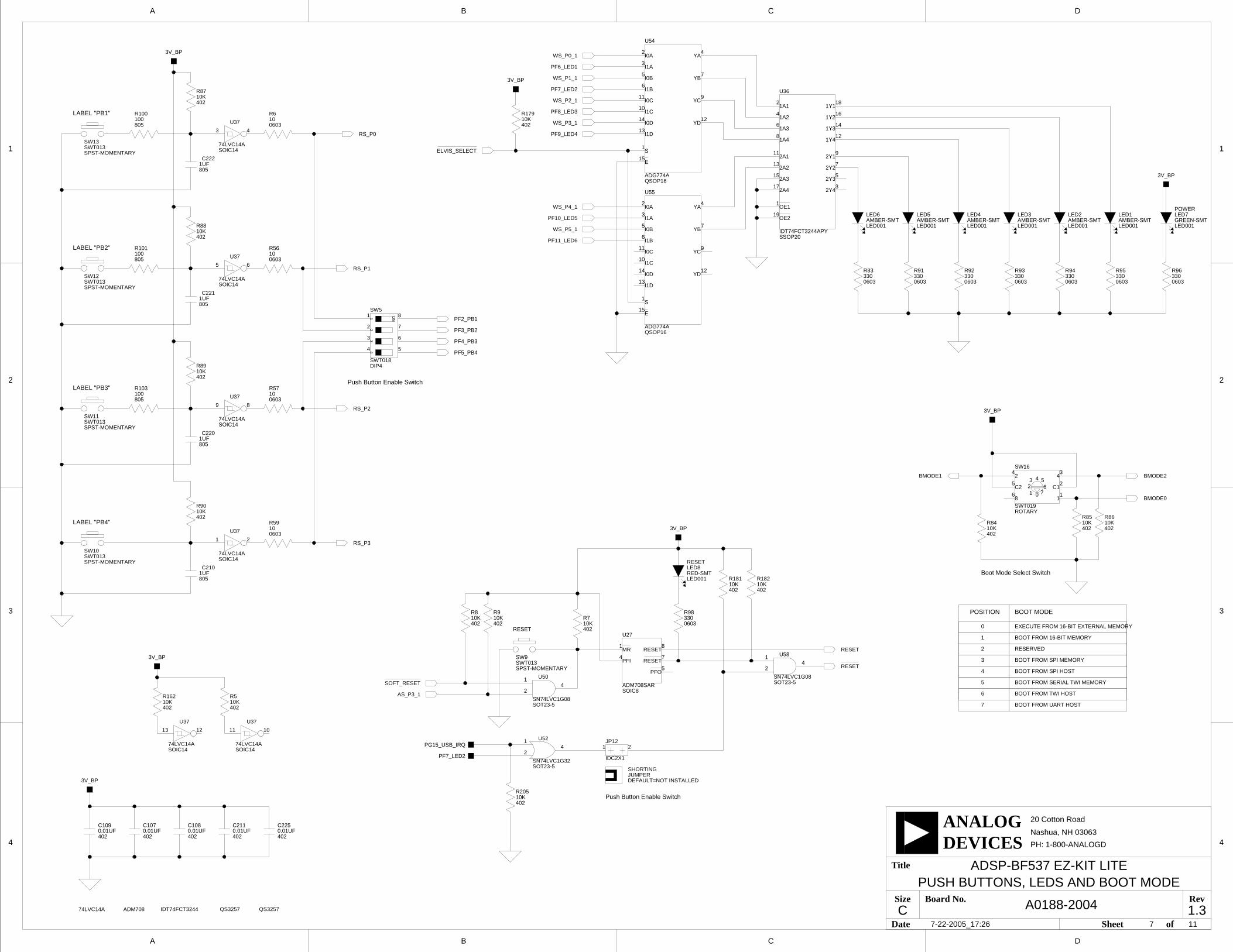
4
3
2
1
A B C D
20 Cotton Road
Nashua, NH 03063
A B C D
4
3
2
1
PH: 1-800-ANALOGD
C
Title
Size Board No.
Date Sheet of
DEVICESANALOG
Rev
ADSP-BF537 EZ-KIT LITE
A0188-2004 1.3
1
C1
4
8
C2
2
0123 4 5
67
1A1
1A2
1A3
1A4
2A2
2A3
2A4
1Y1
1Y2
1Y3
1Y4
2Y1
2Y2
2A1
2Y4
2Y3
OE1
OE2
I0A
I0B
I0C
I0D
I1A
I1B
I1C
I1D
S
YA
YB
YC
YD
E
I0A
I0B
I0C
I0D
I1A
I1B
I1C
I1D
S
YA
YB
YC
YD
E
JUMPERSHORTING
ON1
23
4
PFI
RESETMR
PFO
RESET
QS3257
RESET
POWER
RESET
2
3
4
5
6
7
ADM708
1
EXECUTE FROM 16-BIT EXTERNAL MEMORY
BOOT FROM 16-BIT MEMORY
RESERVED
BOOT FROM SPI MEMORY
BOOT FROM SPI HOST
BOOT FROM SERIAL TWI MEMORY
BOOT FROM TWI HOST
BOOT FROM UART HOST
0
BOOT MODEPOSITION
74LVC14A IDT74FCT3244 QS3257
Boot Mode Select Switch
Push Button Enable Switch
Push Button Enable Switch
LABEL "PB1"
LABEL "PB2"
LABEL "PB3"
LABEL "PB4"
1177-22-2005_17:26
1
24
U58
SOT23-5SN74LVC1G08
4
81
5
7
SOIC8ADM708SAR
U27
21JP12
IDC2X1
R205
40210K
1
24
U52
SOT23-5SN74LVC1G32
8
7
6
54
3
2
1
DIP4SWT018
SW5
DEFAULT=NOT INSTALLED
PF7_LED2
AS_P3_1
10K402
R8
2
5
11
14
3
6
10
13
1
4
7
9
12
15
U55
QSOP16ADG774A
C1080.01UF402
3V_BP
C210
8051UF
1UF805
C220
10K402
R90
3V_BP
1 2
74LVC14ASOIC14
U37 060310R59
5 6
74LVC14ASOIC14
U37
2
5
11
14
3
6
10
13
1
4
7
9
12
15
U54
QSOP16ADG774A
2
4
6
8
13
15
17
18
16
14
12
9
7
11
3
5
1
19
SSOP20IDT74FCT3244APY
U36
R57100603
060310R56
1
2
3
6
5
4SW16
SWT019ROTARY
4020.01UFC109
805100R103
SWT013SPST-MOMENTARY
SW11
89
SOIC1474LVC14A
U37
R6100603
43
74LVC14ASOIC14
U37
R5
40210K10K
402
R162
11 10
SOIC1474LVC14A
U37
R182
40210K
RESET
RESET
R7
40210K
10K402
R179
3V_BP
ELVIS_SELECT
R9
40210K
LED001AMBER-SMTLED6
AMBER-SMTLED001
LED5AMBER-SMTLED001
LED4AMBER-SMTLED001
LED3
LED001AMBER-SMTLED2
AMBER-SMTLED001
LED1GREEN-SMTLED001
LED7
LED001RED-SMTLED8
1213
U37
SOIC1474LVC14A
1
24
SN74LVC1G08SOT23-5
U50
3V_BP
SPST-MOMENTARYSWT013SW10
SWT013SPST-MOMENTARY
SW13
805100R100
SWT013SPST-MOMENTARY
SW9
0603330R98
R9133006030603
330R83
R8610K402402
10KR85
BMODE1
R8410K402
PUSH BUTTONS, LEDS AND BOOT MODE
SPST-MOMENTARYSWT013SW12
100805
R101
BMODE2
BMODE0
4020.01UFC107
10K402
R87
10K402
R88
10K402
R89
0603330R92 R93
3300603 0603
330R94 R95
3300603 0603
330R96
3V_BP
3V_BP
WS_P2_1
WS_P1_1
PF8_LED3
PF7_LED2
WS_P0_1
PF6_LED1
PF9_LED4
WS_P3_1
WS_P5_1
WS_P4_1
PF10_LED5
PF11_LED6
SOFT_RESET
10K402
R181
C221
8051UF
1UF805
C222
4020.01UFC211 C225
0.01UF402
PG15_USB_IRQ
RS_P3
RS_P2
RS_P1
PF4_PB3
PF3_PB2
PF5_PB4
PF2_PB1
RS_P0
3V_BP

4
3
2
1
A B C D
20 Cotton Road
Nashua, NH 03063
A B C D
4
3
2
1
PH: 1-800-ANALOGD
C
Title
Size Board No.
Date Sheet of
DEVICESANALOG
Rev
ADSP-BF537 EZ-KIT LITE
A0188-2004 1.3
A5V
A5V
IN+
IN-
OUT
REF
RG+
RG-
V+
V-
IN+
IN-
OUT
REF
RG+
RG-
V+
V-
JUMPERSHORTING
JUMPERSHORTING
3.3V
AGND
AGND
AGND
A5V
A5V
AGND
AGND
81
24
56
7
ON
3
12
45
6
ON
3
+15_P_1+15_P_2
+5V2
+5V3
+5_P_1+5_P_2+5_P_3
-15_P_1-15_P_2
ACH0ACH1
ACH10ACH11
ACH12ACH13_1ACH14_1ACH15_1
ACH2ACH3
ACH4ACH5_1ACH6_1ACH7_1
ACH8ACH9
AIGND1AIGND2
AIGND3AIGND4
AISENSE_1
AM_1
AS_P[0]_1AS_P[1]_1AS_P[2]_1AS_P[3]_1AS_P[4]_1AS_P[5]_1AS_P[6]_1AS_P[7]_1
DAC0_2 DAC1_2
FG_SIG_1FG_SYNC_1 FM_1
FREQ_OUT
GATE1_1
GND1
ID6ID5ID3ID2
GND10GND11
GND12
GND2
GND13
GND14GND15
GND16GND17
GND3GND4GND5
GND6GND7
GND8GND9
GPCRT1_OUTGPCTR0_GATEGPCTR0_SOURCE
KEY1KEY2KEY3KEY4
KEY5KEY6KEY7KEY8
NC1
NC2
NC3NC4
NC5NC6
NC7NC8
PB_PRES_1
RS_P[0] RS_P[1]RS_P[2] RS_P[3]RS_P[4] RS_P[5]RS_P[6] RS_P[7]
SCANCLKSOURCE1_1
STARTSCAN
TRIG1_2TRIG2
VDCA_1 VDCB_1
VH_1 VL_1
WFTRIG
WS_P[0]_1 WS_P[1]_1WS_P[2]_1 WS_P[3]_1WS_P[4]_1 WS_P[5]_1WS_P[6]_1 WS_P[7]_1
ZH_1ZL_1
ZM_1
CONVERT EXTSRTOBE
GPCTR0_OUT_1
UPDATE
ID0 ID1
ID4ID7
I0A
I0B
I0C
I0D
I1A
I1B
I1C
I1D
S
YA
YB
YC
YD
E
I0A
I0B
I0C
I0D
I1A
I1B
I1C
I1D
S
YA
YB
YC
YD
E
DSP CORE VOLTAGE & CURRENT
ELVIS CONNECTOR
PFI
NI ELVIS ID 30 (0001 1110)
DSP IO CURRENT
Oscilloscope Select Switch
ELVIS Select Jumper
ELVIS Voltage Selection Jumper
Function Generator Switch
1187-22-2005_17:26
2
5
11
14
3
6
10
13
1
4
7
9
12
15
U56
QSOP16ADG774A
15
12
9
7
4
1
13
10
6
3
14
11
5
2
ADG774AQSOP16
U57
A01A02
A22
B28
B55
A03A04A05
B01B02
A48A47
B46B45
B43B42B41B40
A46A45
A43A42A41A40
B48B47
B39A39
B44A44
A49
B54
A28B27A27B26A26B25A25B24
A60 B60
A54A53 B53
B36
A34
B03
B19A19B20A20B21A21B22B23A23
B37
B04
A37
A55B56
B61A61
B05B06A06
B11A11
B18A18
B34B35A35
B12A12B13A13
B50A50B51A51
A24
B49
B52A52
A56B57
B59A59
A29
A10 B10A09 B09A08 B08A07 B07
A32B33
B30
A33B32
A62 B62
A38 B38
B29
B17A16 B16
B15A14 B14
A58A57
B58
A31 B31
A36
A30
A17
A15
P5
PCI32B
0.1R61
0603
R1480.10603
1
2
3
4
5
6 7
8
9
10
11
12SW8
DIP6SWT017
1 2
IDC2X1
JP6
1 2
3 4
P16
IDC2X22X2
21JP8
IDC2X1
8
1
2
7
3
6
5
4
16
15
14
13
12
11
10
9
SW1
SWT016DIP8
4020.01UFC203
VDDINT_SHUNT VDDINT
VDDEXTVDDEXT_SHUNT
DEFAULT=NOT INSTALLED
DEFAULT=NOT INSTALLED
C2260.01UF402
WS_P3_1WS_P5_1
AS_P3_1
PG4_ELVIS_PF6_S
RS_P3
ELVIS_5VELVIS_5V
RS_P2
PG3_ELVIS_PF5
ELVIS_SELECT
PG5_ELVIS_PF7
PG4_ELVIS_PF6
R5890.9K0603
060390.9KR63
25.5KR104
0603
VDDINT_SHUNT
WS_P2_1
3
2
6
U11
SOIC8AD820
R16010K0603
R6011K0603
ELVIS_5V
51
8
4
73
2
6
U2
USOIC8AD623
V_UNREG
R1630402
4020.01UFC202
VDDINT
FUNC_OUT
VDDINT
PG0_ELVIS_TRIGGER_S
ACH0+
FUNC_OUT
R6410K0603
060310KR159
6030.1UFC89
060310KR102
6
2
3
U23
SOIC8AD820
6
2
3 7
4
8
1 5
U3
USOIC8AD623
C880.1UF603
PG3__ELVIS_PF5_S
RS_P1
WS_P1_1
PG5_ELVIS_PF7_S
PG1_ELVIS_PF1_S
DAC1
ACH4+
RS_P0
WS_P0_1
PG3__ELVIS_PF5_SPG2_ELVIS_PF2_S
ACH4+
ACH3+ACH2+ACH1+
DAC0
PG5_ELVIS_PF7_S
PG4_ELVIS_PF6_S
PG2_ELVIS_PF2_S
PG1_ELVIS_PF1_S
PG0_ELVIS_TRIGGER_S
RIGHT_OUT
LEFT_OUT
ELVIS INTERFACE
AMP_LEFT_IN
AMP_RIGHT_IN
ACH3+
PG0_ELVIS_TRIGGER
PG1_ELVIS_PF1
PG2_ELVIS_PF2
AMP_RIGHT_INRIGHT_IN
LEFT_IN
DAC0
DAC1
AMP_LEFT_IN
C2040.01UF402
C2050.01UF402
WS_P4_1
4020.01UFC227
ACH0+
ACH2+
ELVIS_SELECT
ACH1+
4
3
2
1
A B C D
20 Cotton Road
Nashua, NH 03063
A B C D
4
3
2
1
PH: 1-800-ANALOGD
C
Title
Size Board No.
Date Sheet of
DEVICESANALOG
Rev
ADSP-BF537 EZ-KIT LITE
A0188-2004 1.3
3.3V
EXPANSION INTERFACE (TYPE B)
DSP JTAG HEADER
All USB interface circuitry is considered proprietary and has
been omitted from this schematic.
When designing your JTAG interface please refer to the
Engineer to Engineer Note EE-68 which can be found at
http://www.analog.com
7-22-2005_17:26 9 11
10K0603
R105R2150402
1
3
5
7
9
11
13
2
4
6
8
10
12
14
P4
IDC7X27X2
87
85
83
81
77
75
73
69
67
65
63
61
59
57
1
10
1112
1314
1516
1718
19
2
20
2122
2324
2526
2728
29
3
30
3132
3334
3536
3738
39
4
40
4142
4344
4546
4748
5
50
6
78
9
49
55
51
53
52
54
56
58
60
62
66
70
68
72
74
76
78
80
82
84
86
88
90 89
64
71
79
CON01945X2
J3
87
85
83
81
77
75
73
69
67
65
63
61
59
57
1
10
1112
1314
1516
1718
19
2
20
2122
2324
2526
2728
29
3
30
3132
3334
3536
3738
39
4
40
4142
4344
4546
4748
5
50
6
78
9
49
55
51
53
52
54
56
58
60
62
66
70
68
72
74
76
78
80
82
84
86
88
90 89
64
71
79
J2
45X2CON019
87
85
83
81
77
75
73
69
67
65
63
61
59
57
1
10
1112
1314
1516
1718
19
2
20
2122
2324
2526
2728
29
3
30
3132
3334
3536
3738
39
4
40
4142
4344
4546
4748
5
50
6
78
9
49
55
51
53
52
54
56
58
60
62
66
70
68
72
74
76
78
80
82
84
86
88
90 89
64
71
79
J1
45X2CON019
R168
06030
3V_BP
PF3_PB2
PF2_PB1
PF4_PB3
PG3_ELVIS_PF5
PF5_PB4
PF3_PB2 PF2_PB1
PF14_CAN_EN
PF7_LED2
PF11_LED6
PG2_ELVIS_PF2
PG0_ELVIS_TRIGGER
PF4_PB3
PG14PG15_USB_IRQ
PG7_UART0_RTS PG6_UART0_CTS
PG4_ELVIS_PF6
PF9_LED4PF6_LED1
PF8_LED3
PG12
PG10
PG8
PG13
PG11
PG9
PG5_ELVIS_PF7
EMULATOR_SELECT
5V_EI
D14
D[0:15]
D3
D5
D7
D9
D11
D13
D15
D1 D0
D2
D4
D6
D8
D10
D12
3V_BP
PG11
PF13_CAN_ERR
EXPANSION INTERFACE
SCLK
A2
A18
A16
A14
A12
A10
A8
A6
A4
A1
A19
A17
A15
A13
A11
A9
A7
A5
A3
A[1:19]
PJ9_TSCLK0
PG13 PG10
PJ6_RSCLK0
ABE1
SRAS
SWE
PF12_AUDIO_RESET
PG9
PG15_USB_IRQ
PG14
PG12
PG8
ARE
SMS
SCKE
AMS0
AMS1
AMS2
AMS3
ARDY
ABE1
AWE
SA10 SCAS
ABE0
AOE
PJ4_CAN_RX
PJ8_DR0PRI
PJ7_RFS0PJ10_TFS0
PJ11_DT0PRI
PJ5_CAN_TX
PF14_CAN_EN
ABE0
EMULATOR_EMU
EMULATOR_TRST
EMULATOR_TDI
EMULATOR_TDO
EMULATOR_TMS
EMULATOR_TCK
NMI
POE_VCC+
PF0_UART0_TX
POE_VCC-
PG1_ELVIS_PF1
PF15_CAN_STB~
PF7_LED2
PF6_LED1
PF6_LED1
PJ1_MDIO
PH5_TXCLK PH4_ETXEN
PH2_ETXD2
PH1_ETXD1 PH0_ETXD0
PF2_PB1
RESET
RESET
BR
BG
BGH
PF0_UART0_TX PF1_UART0_RX
PF3_PB2
PH13_ERXCLK
PH7_COL
PJ0_MDC
PH14_ERXER
3V_BP5V_EI
PJ2_SCLPJ3_SDA
CLKBUF
PH6_PHYINT
PH8_ERXD0PH9_ERXD1
PH10_ERXD2PH11_ERXD3
PH12_ERXDV
PH3_ETXD3
PH15_CRS
PF10_LED5
3.3V
4
3
2
1
A B C D
20 Cotton Road
Nashua, NH 03063
A B C D
4
3
2
1
PH: 1-800-ANALOGD
C
Title
Size Board No.
Date Sheet of
DEVICESANALOG
Rev
ADSP-BF537 EZ-KIT LITE
A0188-2004 1.3
5V 3.3V
3.3V 5V
3.3V
3.3V5V
5V
5V
JUMPERSHORTING
5V 3.3V 5V 3.3V
ON1
23
4
C1+
C1-
C2+
C2-
R1INR1OUT
R2INR2OUT
T1OUT
T2IN T2OUT
V-
V+
T1IN
(UART 0)SERIAL PORT
UART 0 Loop Jumper
SPORT 1
TIMERS
PPI
TWI
SPI
SPORT 0
UART 1
UART Enable Switch
11107-22-2005_17:26
4020.1UFC114
1
3
4
5
1312
89
14
10 7
6
2
11
U32
ADM3202ARNSOIC16
4020.1UFC112
C1130.1UF402
8
7
6
54
3
2
1
DIP4SWT018
SW43
4
5
1
6
2
7
8
9
J6
9PINCON038
2
1JP9
IDC2X1
402DNPR204
5
2
4
8
10
6
1
3
9
11
13
15
17
19
12
14
16
20
18
7
P9
IDC10X210X2
12
7
31
3
6
4
11
9
8
5
34 33
32
30 29
28 27
26 25
24 23
22 21
20 19
18 17
16 15
14 13
12
10
P7
IDC17X217X2
10
12
1314
1516
1718
1920
2122
2324
2526
2728
2930
32
3334
5
8
9
11
4
6
3
31
7
2 1P6
IDC17X217X2
DEFAULT=NOT INSTALLED
R203DNP402
PJ11_DT0PRI
C1110.1UF402
PF12_AUDIO_RESET
PG4_ELVIS_PF6
PJ5_CAN_TX
PF5_PB4
PF10_LED5PF14_CAN_EN
PF6_LED1
PF4_PB3
PF0_UART0_TX
PF1_UART0_RX
5
9
8 7
6
4 3
2
10
1
5X2IDC5X2
P12
1
10
2
34
6
78
9
5
P11
IDC5X25X2
7
18
20
16
14
12
19
17
15
13
11
9
3
1
6
10
8
4
2
5
P10
IDC10X210X2
1
10
1112
1314
1516
1718
19
2
20
2122
2324
2526
2728
29
3
30
3132
3334
3536
3738
39
4
40
56
78
9
P8
IDC20X220X2
V_UNREG
V_UNREG
V_UNREGV_UNREG
PF9_LED4
PF10_LED5PF14_CAN_EN
PF15_CAN_STB~
3V_BP
PF4_PB3
PF6_LED1
PF2_PB1
PJ2_SCL
PJ3_SDA
PF3_PB2
PG3_ELVIS_PF5
PF11_LED6
PF13_CAN_ERR
PF9_LED4
PJ6_RSCLK0
PJ5_CAN_TX
PJ4_CAN_RX
PJ8_DR0PRI
PJ9_TSCLK0
PJ11_DT0PRI
STAMP CONNECTORS
PF11_LED6
PF12_AUDIO_RESET
PF13_CAN_ERR
PJ3_SDA
PJ2_SCL
PF8_LED3
PF7_LED2
PF13_CAN_ERR
PF11_LED6PF12_AUDIO_RESET
RESET
RESET
PG8
PG2_ELVIS_PF2
PG0_ELVIS_TRIGGER
PF15_CAN_STB~
PG6_UART0_CTS
PG9
PG13
PG11
PG15_USB_IRQ
PG10
PG14
PG12
PG5_ELVIS_PF7
PG7_UART0_RTS
PG1_ELVIS_PF1
PG14
PF9_LED4
PG10
PG11
PG9
PG8
PG12
PG13
PG15_USB_IRQ
PJ3_SDA
PJ2_SCL
PF8_LED3
PF7_LED2
PF11_LED6
PF13_CAN_ERR
PF12_AUDIO_RESET
RESET
PF2_PB1
PF4_PB3PF9_LED4
PF8_LED3
PF7_LED2
PF3_PB2
PG7_UART0_RTS
PG6_UART0_CTS
PJ10_TFS0
PG6_UART0_CTS
PG4_ELVIS_PF6
PG2_ELVIS_PF2
PG0_ELVIS_TRIGGER PG1_ELVIS_PF1
PG3_ELVIS_PF5
PG5_ELVIS_PF7
PG7_UART0_RTS
RESET
PJ3_SDA PJ2_SCL
V_UNREG
PJ10_TFS0
PJ7_RFS0
RESET
PF8_LED3
PF9_LED4
PF7_LED2
PJ10_TFS0
PF6_LED1
PF5_PB4
PF4_PB3
PJ5_CAN_TX
PF14_CAN_EN
PF10_LED5
PJ11_DT0PRIPJ11_DT0PRI
PF10_LED5
PF14_CAN_EN
PJ5_CAN_TX
PF4_PB3
PF5_PB4
PF6_LED1
PJ10_TFS0
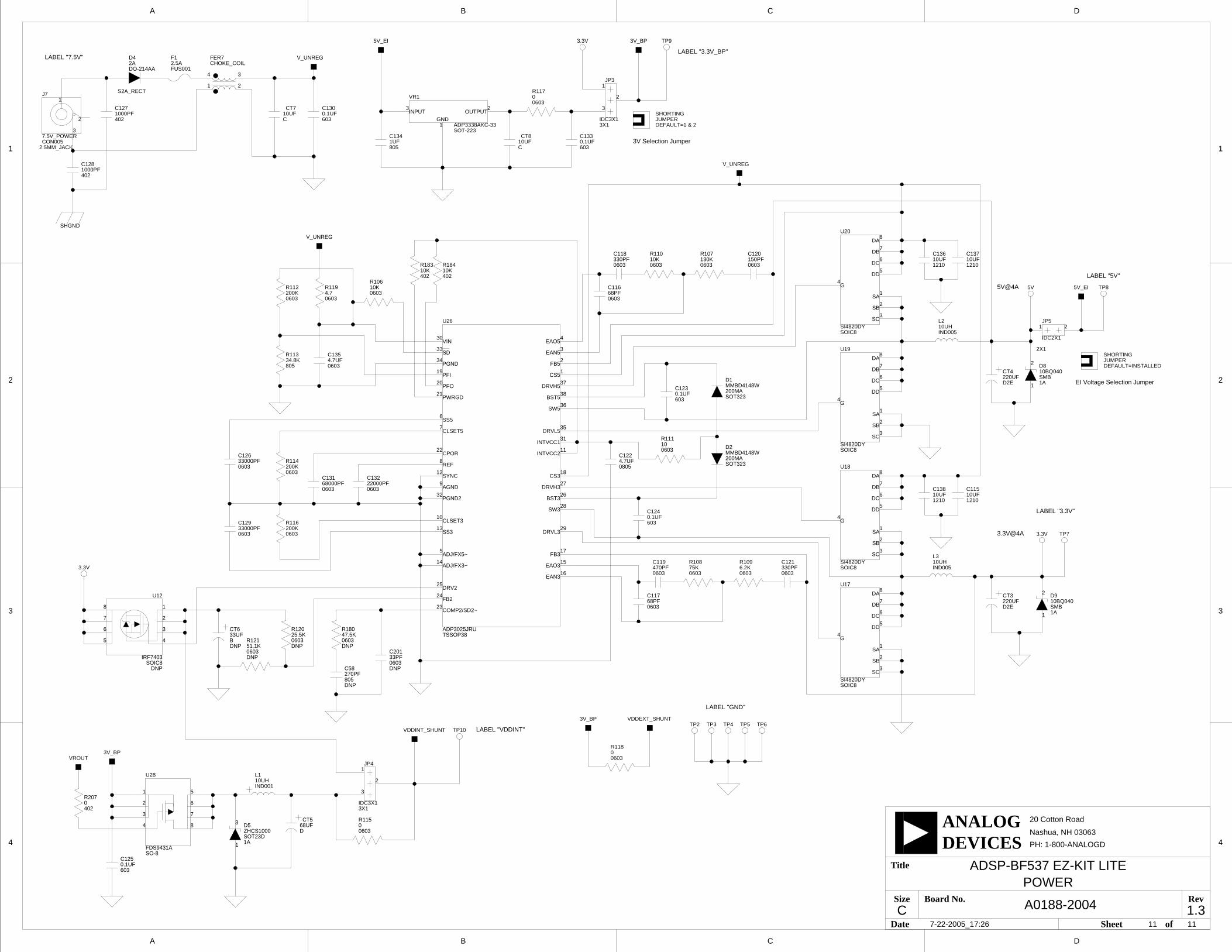
4
3
2
1
A B C D
20 Cotton Road
Nashua, NH 03063
A B C D
4
3
2
1
PH: 1-800-ANALOGD
C
Title
Size Board No.
Date Sheet of
DEVICESANALOG
Rev
ADSP-BF537 EZ-KIT LITE
A0188-2004 1.3
DA
DB
DC
DD
G
SA
SB
SC
DA
DB
DC
DD
G
SA
SB
SC
DA
DB
DC
DD
G
SA
SB
SC
DA
DB
DC
DD
G
SA
SB
SC
JUMPERSHORTING
ADJ/FX3~
ADJ/FX5~
AGND
PGND2 BST3
BST5
CLSET3
CLSET5
COMP2/SD2~
CPOR
CS3
CS5
DRV2
DRVH3
DRVH5
DRVL3
DRVL5
EAN3
EAN5
EAO3
EAO5
FB2
FB3
FB5
INTVCC1
INTVCC2
PFI
PFO
PGND
PWRGD
REF
SS3
SS5
SW3
SW5
SYNC
VIN
SD
TSSOP38
JUMPERSHORTING
SHGND
3.3V
3.3V
5V
3.3V
CHOKE_COIL
GNDINPUT OUTPUT
LABEL "7.5V"
LABEL "GND"
LABEL "VDDINT"
3V Selection Jumper
LABEL "3.3V_BP"
LABEL "5V"
EI Voltage Selection Jumper
3.3V@4A
5V@4A
LABEL "3.3V"
7-22-2005_17:26 11 11
00603
R115
3
1
2
JP4
IDC3X13X1
C201
DNP
33PF0603
C58
DNP
270PF805
R180
DNP
47.5K0603
R120
DNP
25.5K0603R121
51.1K0603DNP
CT6
DNP
33UFB5
6
7
8
4
1
2
3
U12
SOIC8IRF7403
DNP
1
2
3
JP3
IDC3X13X1
6030.1UFC133
00603
R117
CT810UFC
2
1
3
ADP3338AKC-33SOT-223
VR1
8051UFC134
R183
40210K
R118
06030
1
2
SMB10BQ040
1A
D9CT3220UFD2E
TP10
TP9
TP8
TP7
6030.1UFC130CT7
10UFC
4
1
3
2
FER7
FUS0012.5AF1
4021000PFC127
DO-214AA
S2A_RECT
2AD4
4021000PFC128
1
3
2
CON0052.5MM_JACK
7.5V_POWER
J7
4
3
2
1
8
7
6
5
U28
SO-8FDS9431A
0402
R207
D2
SOT323
MMBD4148W200MA
D1
SOT323
MMBD4148W200MA
VROUT
5V_EI
DEFAULT=INSTALLED
VDDINT_SHUNT
3V_BP
16
15
17
29
28
26
27
18
11
31
35
36
38
37
1
2
3
4
23
24
25
14
5
13
10
32
9
12
8
22
7
6
21
20
19
34
30
33
U26
ADP3025JRU
TP5 TP6TP2
DEFAULT=1 & 2
D2E220UFCT4
06036.2KR109 C121
330PF0603
C120150PF0603
R107130K0603
06034.7R119
C1354.7UF0603
3
2
1
4
5
6
7
8U20
SOIC8SI4820DY
8
7
6
5
4
1
2
3
U17
SOIC8SI4820DY
3
2
1
4
5
6
7
8U18
SOIC8SI4820DY
8
7
6
5
4
1
2
3
U19
SOIC8SI4820DY
1
2 D8
1A
10BQ040SMB
IND00510UHL3
3
1 1A
ZHCS1000SOT23D
D5
3V_BP
R10610K0603
0603200KR114
C1230.1UF603
C118330PF0603
R11010K0603
060375KR108
5V_EI
R11334.8K805
R112200K0603
CT5
D68UF
L210UHIND005
6030.1UFC124
C1224.7UF0805
C119470PF0603
060368PFC117
C11668PF0603
C13610UF1210
C12933000PF0603
R116200K0603
C13168000PF0603
C13222000PF0603
POWER
C12633000PF0603
121010UFC137
C11510UF12101210
10UFC138
R111100603
IND00110UHL1
C125
6030.1UF
10K402
R184
TP3 TP4
1 2
2X1
IDC2X1
JP5
V_UNREG
V_UNREG
VDDEXT_SHUNT3V_BP
V_UNREG
I INDEX
A ~AMS3-0 (flash select) pins, 1-9, 2-3, 2-10
AD1854, digital-to-analog converter (DAC), 1-12
AD1871, analog-to-digital converter (CAD), 1-12
ADSP-BF537 processorsaudio interface (SPORT0), 1-12, 2-3boot modes, 2-12clock out (CLK OUT), 2-3core and IO voltage, 2-2Ethernet peripherals, 1-11ETXDx/ERXDx signals, 2-6external bus interface unit (EBIU), 2-3general-purpose IO pins, 2-8, 2-9, 2-10, 2-11,
2-19GPIO (general-purpose input/output) pins,
2-4input clock, 2-3internal memory (SRAM), 1-6memory select pins, See ~AMS3-0; ~SMS0peripheral ports, xiiiPPIx signals, 2-5programmable flag pins (PFs), 1-13, 2-18real time clock (RTC), 2-3SPI signals, 2-5TMRx signals, 2-4UARTx signals, 2-4
analog audio interface, See audio interfacearchitecture, of this EZ-KIT Lite, 2-2ASYNC (asynchronous memory control)
external memory banks 0-3, 1-7register, 1-10
audiocircuit, 1-12, 2-3, 2-14connectors (J9-10), 2-21DAC/CAD, See AD1854; AD1871enable switch (SW7), 2-11input configuration switch (SW8), 2-14interface, xiii, 1-12, 2-3reset pin (PF12), 2-5
Bbackground telemetry channel (BTC), 1-14bill of materials, A-1boot
modes, 2-12mode select switch (SW16), 2-12
Cclock frequency, 1-8COL signals, 2-6configuration, of this EZ-KIT Lite, 1-3
ADSP-BF537 EZ-KIT Lite Evaluation System Manual I-1
INDEX
connectorsmap of locations, 2-20DB9 (UART), 2-7J1-3 (expansion), 2-3, 2-7, 2-23J4 (Ethernet), 2-21J5 and J11 (CAN), 2-21J6 (RS-232), 2-22J7 (power), 2-22J9-10 (audio), 2-21P10 (TWI), 2-25P11 (timers), 2-25P12 (UART1), 2-26P4 (JTAG), 2-8, 2-23P6 (SPORT0), 1-12, 2-3, 2-24P7 (SPORT1), 2-24P8 (PPI), 2-24P9 (SPI), 2-4, 2-25
contents, this EZ-KIT Lite package, 1-2Controller Area Network (CAN), xii
connectors (J5 and J11), 2-21enable switch (SW2), 2-8interface, xii, 1-10signals, 2-5, 2-9transceiver, 1-10
customer support, xv
Ddata acquisition (DAQ) device, 1-12DB9 (UART) connector, xiii, 2-7default configuration, of this EZ-KIT Lite, 1-3,
1-4DIP switch (SW5), 1-4, 1-13
EEBIU_SDBCTL register, 1-8, 1-9EBIU_SDGCTL register, 1-8, 1-9EBIU_SDRRC register, 1-8, 1-9
Educational Laboratory Virtual Instrumentation Suite interface, See ELVIS
ELVIS (Educational Laboratory Virtual Instrumentation Suite)
interface, xii, 1-11, 2-14select jumper (JP8), 2-16signals, 2-5voltage select jumper (JP6), 2-15
enable control input (EN), 1-10error/power indication output (ERR), 1-10ERXD signals, 2-6Ethernet
cables, 1-3connector (J4), 2-21interface, xii, 1-11, 2-6select switch (SW3), 2-9
ETXD signals, 2-6example programs, 1-13expansion interface, 1-9, 1-12, 2-3, 2-4, 2-7,
2-10, 2-23voltage select jumper (JP5), 2-13
external bus interface unit (EBIU), 2-3external memory, 1-7, 2-3, 2-8
Ffeatures, of this EZ-KIT Lite, xiflag pins, See programmable flags (PFs)flash memory, xi, xiii, 1-9, 2-3, 2-12
address range switch, 1-9enable (SW6) switch, 2-10
frame sync signals, 1-12frequency, 1-8
Ggeneral-purpose input/output, 1-13
HHelp, online, xx
I-2 ADSP-BF537 EZ-KIT Lite Evaluation System Manual

INDEX
IIEEE 802.3-2002 standard, 1-11installation, of this EZ-KIT Lite, 1-5interfaces
analog audio, xi, 1-12, 2-3Controller Area Network (CAN), xii, 1-10ELVIS, 1-11Ethernet, -xii, 1-11expansion, 1-12, 2-23SDRAM, 1-8
internal memory, 2-8core MMRs, 1-7data bank A SRAM, 1-7data bank A SRAM/CACHE, 1-7data bank B SRAM, 1-7data bank B SRAM/CACHE, 1-7instruction bank A SRAM, 1-7instruction bank B SRAM, 1-7instruction SRAM/CACHE, 1-7map, 1-7reserved, 1-7scratch pad SRAM, 1-7system MMRs, 1-7
internal regulator, 2-2IO voltage, 2-2
JJTAG
connector (P4), 2-23emulation port, 2-8
jumpersmap of locations, 2-8JP3 (power), 2-12JP5 (expansion voltage), 2-13JP6 (ELVIS voltage), 2-15JP8 (ELVIS select), 2-16JP9 (UART), 2-13
LLabVIEW virtual instruments, xii, 1-12LEDs
map of locations, 2-17LED10 (USB monitor), 1-5, 2-19LED1-6 (PF6-11), 1-13, 2-5, 2-19LED7 (power), 2-18LED8-9 (reset), 2-18
license restrictions, xi, 1-6
MMAC address, xii, 1-7, 1-10, 1-11Media Access Controller, See MACMedia Instruction Set Computing (MISC), ixmemory
default configuration, 1-10map, 1-6select pins, See ~AMS3-0; ~SMS0
Micro Signal Architecture (MSA), ixMISC (Media Instruction Set Computing), ixMSA (Micro Signal Architecture), ix
Nnotation conventions, xxii
Ooscilloscope configuration switch (SW1), 2-14
Ppackage contents, 1-2PG0-15 pins, 2-5PH0-15 signals, 2-6
ADSP-BF537 EZ-KIT Lite Evaluation System Manual I-3

INDEX
powerconnector (J7), 2-22LED (LED7), 2-18regulator circuit, 2-12, 2-13select jumper (JP3), 2-12specifications, 2-22supply, 1-3, 2-22
Power-over-Ethernet (PoE), 1-11, 2-12, 2-13PPI connector (P8), 2-24programmable flags (PFs)
connections, 2-4PF0-1 (UART), 2-4PF12 (audio), 2-5PF13-15 (CAN), 1-10, 2-5PF2-5, 1-13, 2-4, 2-18PF6-11 (IO), 1-13, 2-5, 2-19
push buttonsSee also switches by name (SWx)locations, 2-17
Rreceive data output (RXD), 1-10Reduced Instruction Set Computing (RISC), ixregistration, this product, 1-3regulators, 2-2reset
processor, 2-18push button (SW9), 2-17
restrictions, licence, 1-6RISC (Reduced Instruction Set Computing), ixRJ45 connector, 1-11RS-232 connector (J6), xiii, 2-22
SSCLK, See system clock (SCLK)
SDRAM, xi, xiii, 1-6, 1-7, 2-3bank 0, 1-7, 1-8default settings, 1-8interface, 1-8optimum settings, 1-9
serial clock (SCL), 1-8serial peripheral interconnect (SPI)
connector (P9), 2-25interface, 2-4
setup, of this EZ-KIT Lite hardware, 1-4~SMS0 (SDRAM select) pin, 1-6, 2-3SPORT0
connector (P6), 2-24interface, xiii, 1-12, 2-3
SPORT1connector (P7), 2-24
standby control input (~STB), 1-10startup, of this EZ-KIT Lite, 1-5stereo input/output channels, 1-12SW10-13 (PF2-5), 2-4, 2-18SW16 (boot mode select) switch, 2-12SW1 (audio/oscilloscope) switch, 2-14SW2 (CAN enable) switch, 1-10, 2-8SW3 (Ethernet) switch, 2-9SW4 (UART) switch, 2-9SW5 (push button enable) DIP switch, 1-13,
2-10, 2-18SW6 (flash enable) switch, 1-9, 2-10SW7 (audio enable) switch, 1-12, 2-11SW8 (audio input) switch, 2-14SW9 (reset), 2-17switches
See also switches by name (SWx)map of locations, 2-8
synchronous dynamic random access memory, See SDRAM
systemarchitecture, of this EZ-KIT Lite, 2-2clock frequency, 1-8
I-4 ADSP-BF537 EZ-KIT Lite Evaluation System Manual
INDEX
TTarget Options dialog box, 1-8timers connector (P11), 2-25transmit data input (TXD), 1-10TWI connector (P10), 2-25two-wire interface (TWI), 1-12, 2-25
UUART
enable switch (SW4), 2-9loop jumper (JP9), 2-13port, 2-7
UART0signals, 2-6transmit/receive, 2-4
UART1 connector (P12), 2-26universal asynchronous receiver transmitter, See
UART
USBbus power, 2-6, 2-12, 2-13cable, 1-3connector (P7), 2-22interface, xi, 2-8, 2-23interface chip, 2-17, 2-18monitor LED (LED10), 2-19
USB-LAN EZ-Extender, 1-11, 2-12, 2-13user LEDs (LED1-6), 2-19
Vvery-long instruction word (VLIW), ixVisualDSP++
documentation, xxionline Help, xx
VLIW (very-long instruction word), ixvoltage regulators, 2-2
ADSP-BF537 EZ-KIT Lite Evaluation System Manual I-5
INDEX
I-6 ADSP-BF537 EZ-KIT Lite Evaluation System Manual