ADSP-2106x SHARC Processor User’s Manual...a ADSP-2106x SHARC® Processor User’s Manual Revision...
698
a ADSP-2106x SHARC ® Processor User’s Manual Revision 2.1, March 2004 Part Number 82-000795-03 Analog Devices, Inc. One Technology Way Norwood, Mass. 02062-9106
Transcript of ADSP-2106x SHARC Processor User’s Manual...a ADSP-2106x SHARC® Processor User’s Manual Revision...
a
ADSP-2106x SHARC® ProcessorUser’s Manual
Revision 2.1, March 2004
Part Number82-000795-03
Analog Devices, Inc.One Technology WayNorwood, Mass. 02062-9106
Copyright Information© 2004 Analog Devices, Inc., ALL RIGHTS RESERVED. This document may not be reproduced in any form without prior, express written consent from Analog Devices, Inc.
Printed in the USA.
DisclaimerAnalog Devices, Inc. reserves the right to change this product without prior notice. Information furnished by Analog Devices is believed to be accurate and reliable. However, no responsibility is assumed by Analog Devices for its use; nor for any infringement of patents or other rights of third parties which may result from its use. No license is granted by implication or otherwise under the patent rights of Analog Devices, Inc.
Trademark and Service Mark NoticeThe Analog Devices logo, EZ-ICE, EZ-LAB, SHARC, and the SHARC logo are registered trademarks of Analog Devices, Inc.
All other brand and product names are trademarks or service marks of their respective owners.
Errata Correction NoticeThis revision is published to incorporate corrections to errata in the Second Edition (May 1997). Please refer to Appendix H for more information.
iii
Contents
CHAPTER 1 INTRODUCTION
1.1 OVERVIEW ..........................................................................................................1-11.2 ADSP-21000 FAMILY FEATURES & BENEFITS ................................................1-51.2.1 System-Level Enhancements ..........................................................................1-61.2.2 Why Floating-Point DSP? ................................................................................1-71.3 ADSP-2106X ARCHITECTURE ...........................................................................1-81.3.1 Core Processor ................................................................................................1-81.3.1.1 Computation Units .......................................................................................1-81.3.1.2 Data Register File ........................................................................................1-81.3.1.3 Program Sequencer & Data Address Generators .......................................1-91.3.1.4 Instruction Cache.......................................................................................1-101.3.1.5 Interrupts....................................................................................................1-101.3.1.6 Timer..........................................................................................................1-101.3.1.7 Core Processor Buses ...............................................................................1-101.3.1.8 Internal Data Transfers ..............................................................................1-111.3.1.9 Context Switching ......................................................................................1-111.3.1.10 Instruction Set ............................................................................................1-121.3.2 Dual-Ported Internal Memory .........................................................................1-121.3.3 External Memory & Peripherals Interface ......................................................1-131.3.4 Host Processor Interface ...............................................................................1-131.3.5 Multiprocessing ..............................................................................................1-141.3.6 I/O Processor .................................................................................................1-141.3.6.1 Serial Ports ................................................................................................1-141.3.6.2 Link Ports ...................................................................................................1-151.3.6.3 DMA Controller ..........................................................................................1-151.3.6.4 Booting.......................................................................................................1-161.4 DEVELOPMENT TOOLS ...................................................................................1-161.5 MESH MULTIPROCESSING .............................................................................1-181.6 ADDITIONAL LITERATURE ..............................................................................1-18
CHAPTER 2 COMPUTATION UNITS
2.1 OVERVIEW ..........................................................................................................2-12.2 IEEE FLOATING-POINT OPERATIONS .............................................................2-22.2.1 Extended Floating-Point Precision ...................................................................2-32.2.2 Short Word Floating-Point Format ...................................................................2-32.2.3 Floating-Point Exceptions ................................................................................2-42.3 FIXED-POINT OPERATIONS ..............................................................................2-42.4 ROUNDING ..........................................................................................................2-4
Contents
iv
2.5 ALU ......................................................................................................................2-52.5.1 ALU Operation .................................................................................................2-62.5.2 ALU Operating Modes .....................................................................................2-62.5.2.1 Saturation Mode ..........................................................................................2-72.5.2.2 Floating-Point Rounding Modes ..................................................................2-72.5.2.3 Floating-Point Rounding Boundary ..............................................................2-72.5.3 ALU Status Flags .............................................................................................2-72.5.3.1 ALU Zero Flag (AZ) .....................................................................................2-82.5.3.2 ALU Underflow Flag (AZ, AUS) ...................................................................2-82.5.3.3 ALU Negative Flag (AN) ..............................................................................2-82.5.3.4 ALU Overflow Flag (AV, AOS, AVS) ...........................................................2-82.5.3.5 ALU Fixed-Point Carry Flag (AC) ................................................................2-92.5.3.6 ALU Sign Flag (AS) .....................................................................................2-92.5.3.7 ALU Invalid Flag (AI) ...................................................................................2-92.5.3.8 ALU Floating-Point Flag (AF) ......................................................................2-92.5.3.9 Compare Accumulation ....................................................................................2-92.5.4 ALU Instruction Summary ..............................................................................2-102.6 MULTIPLIER ......................................................................................................2-112.6.1 Multiplier Operation ........................................................................................2-112.6.2 Fixed-Point Results ........................................................................................2-122.6.2.1 MR Registers .............................................................................................2-122.6.3 Fixed-Point Operations ..................................................................................2-132.6.3.1 Clear MR Register .....................................................................................2-132.6.3.2 Round MR Register ...................................................................................2-142.6.3.3 Saturate MR Register On Overflow ...........................................................2-142.6.4 Floating-Point Operating Modes ....................................................................2-152.6.4.1 Floating-Point Rounding Modes ................................................................2-152.6.4.2 Floating-Point Rounding Boundary ............................................................2-152.6.5 Multiplier Status Flags ....................................................................................2-152.6.5.1 Multiplier Underflow Flag (MU) ..................................................................2-162.6.5.2 Multiplier Negative Flag (MN) ....................................................................2-172.6.5.3 Multiplier Overflow Flag (MV) ....................................................................2-172.6.5.4 Multiplier Invalid Flag (MI) .........................................................................2-172.6.6 Multiplier Instruction Summary.......................................................................2-182.7 SHIFTER ............................................................................................................2-192.7.1 Shifter Operation ............................................................................................2-192.7.2 Bit Field Deposit & Extract Instructions ..........................................................2-202.7.3 Shifter Status Flags........................................................................................2-242.7.3.1 Shifter Zero Flag (SZ) ................................................................................2-242.7.3.2 Shifter Overflow Flag (SV) .........................................................................2-242.7.3.3 Shifter Sign Flag (SS) ................................................................................2-242.7.4 Shifter Instruction Summary ...........................................................................2-25

Contents
v
2.8 MULTIFUNCTION COMPUTATIONS ................................................................2-262.9 REGISTER FILE ................................................................................................2-272.9.1 Alternate (Secondary) Registers ....................................................................2-28
CHAPTER 3 PROGRAM SEQUENCING
3.1 OVERVIEW ..........................................................................................................3-13.1.1 Instruction Cycle ..............................................................................................3-23.1.2 Program Sequencer Architecture .....................................................................3-33.1.2.1 Program Sequencer Registers & System Registers ....................................3-53.2 PROGRAM SEQUENCER OPERATIONS ..........................................................3-63.2.1 Sequential Instruction Flow ..............................................................................3-63.2.2 Program Memory Data Accesses ....................................................................3-63.2.3 Branches ..........................................................................................................3-63.2.4 Loops ...............................................................................................................3-63.3 CONDITIONAL INSTRUCTION EXECUTION .....................................................3-73.4 BRANCHES (CALL, JUMP, RTS, RTI) ................................................................3-93.4.1 Delayed & Nondelayed Branches ..................................................................3-103.4.2 PC Stack ........................................................................................................3-123.5 LOOPS (DO UNTIL) ...........................................................................................3-133.5.1 Restrictions & Short Loops ............................................................................3-143.5.1.1 General Restrictions ..................................................................................3-143.5.1.2 Counter-Based Loops ................................................................................3-153.5.1.3 Non-Counter-Based Loops ........................................................................3-163.5.2 Loop Address Stack .......................................................................................3-183.5.3 Loop Counters And Stack ..............................................................................3-193.5.3.1 CURLCNTR ...............................................................................................3-193.5.3.2 LCNTR .......................................................................................................3-203.6 INTERRUPTS ....................................................................................................3-213.6.1 Interrupt Latency ............................................................................................3-223.6.2 Interrupt Vector Table ....................................................................................3-243.6.3 Interrupt Latch Register (IRPTL) ....................................................................3-263.6.4 Interrupt Priority..............................................................................................3-273.6.5 Interrupt Masking & Control ...........................................................................3-273.6.5.1 Interrupt Mask Register (IMASK) ...............................................................3-273.6.5.2 Interrupt Nesting & IMASKP ......................................................................3-283.6.6 Status Stack Save & Restore .........................................................................3-293.6.7 Software Interrupts .........................................................................................3-293.6.8 Clearing The Current Interrupt For Reuse .....................................................3-303.6.9 External Interrupt Timing & Sensitivity ...........................................................3-31
Contents
vi
3.6.9.1 Asynchronous External Interrupts .............................................................3-323.6.10 Multiprocessor Vector Interrupts (VIRPT) ......................................................3-323.7 TIMER ................................................................................................................3-333.7.1 Timer Enable/Disable.....................................................................................3-343.7.2 Timer Interrupts..............................................................................................3-353.7.3 Timer Registers..............................................................................................3-363.8 STACK FLAGS...................................................................................................3-363.9 IDLE & IDLE16 ...................................................................................................3-373.10 INSTRUCTION CACHE .....................................................................................3-383.10.1 Cache Architecture ........................................................................................3-383.10.2 Cache Efficiency ............................................................................................3-393.10.3 Cache Disable & Cache Freeze.....................................................................3-41
CHAPTER 4 DATA ADDRESSING
4.1 OVERVIEW ..........................................................................................................4-14.2 DAG REGISTERS ................................................................................................4-14.2.1 Alternate DAG Registers..................................................................................4-34.3 DAG OPERATION ...............................................................................................4-44.3.1 Address Output & Modification ........................................................................4-44.3.1.1 DAG Modify Instructions ..............................................................................4-54.3.1.2 Immediate Modifiers ....................................................................................4-64.3.2 Circular Buffer Addressing ...............................................................................4-64.3.2.1 Circular Buffer Operation .............................................................................4-74.3.2.2 Circular Buffer Registers .............................................................................4-84.3.2.3 Circular Buffer Overflow Interrupts ..............................................................4-84.3.3 Bit-Reversal ...................................................................................................4-104.3.3.1 Bit-Reverse Mode ......................................................................................4-104.3.3.2 Bit-Reverse Instruction ..............................................................................4-104.4 DAG REGISTER TRANSFERS .........................................................................4-114.4.1 DAG Register Transfer Restrictions...............................................................4-12
CHAPTER 5 MEMORY
5.1 OVERVIEW ..........................................................................................................5-15.1.1 Dual Data Accesses .........................................................................................5-35.1.2 Instruction Cache & PM Bus Data Accesses ...................................................5-45.1.3 On-Chip Memory Buses & Address Generation ..............................................5-55.1.4 Bus Exchange (PX Registers) .........................................................................5-65.1.5 Memory Block Accesses & Conflicts................................................................5-8
Contents
vii
5.2 ADSP-2106X MEMORY MAP ..............................................................................5-95.2.1 ADSP-21060 Internal Memory Space ............................................................5-115.2.2 ADSP-21062 Internal Memory Space ............................................................5-145.2.3 ADSP-21061 Internal Memory Space ............................................................5-165.2.4 Porting Code from ADSP-21060 to ADSP-21062 or ADSP-21061 ................5-185.2.5 Multiprocessor Memory Space ......................................................................5-185.2.6 External Memory Space .................................................................................5-195.2.7 Memory Space Access Restrictions ..............................................................5-195.3 INTERNAL MEMORY ORGANIZATION & WORD SIZE ...................................5-205.3.1 32-Bit Words & 48-Bit Words .........................................................................5-205.3.2 Mixing 32-Bit & 48-Bit Words In One Memory Block .....................................5-235.3.3 Basic Examples Of Mixed 32-Bit & 48-Bit Words ..........................................5-245.3.4 16-Bit Short Words .........................................................................................5-275.3.5 Mixing 32-Bit & 48-Bit Words With Finer Granularity .....................................5-285.3.5.1 Low-Level Physical Mapping Of Memory Blocks .......................................5-295.3.5.2 Placement Restrictions For Mixed 32-Bit & 48-Bit Words .........................5-305.3.5.3 Shadow Write FIFO ...................................................................................5-335.3.6 Configuring Memory For 32-Bit or 40-Bit Data ...............................................5-345.4 EXTERNAL MEMORY INTERFACING ..............................................................5-355.4.1 External Memory Banks .................................................................................5-385.4.2 Unbanked Memory .........................................................................................5-385.4.3 Boot Memory Select (BMS) ...........................................................................5-395.4.4 Wait States & Acknowledge ...........................................................................5-395.4.4.1 WAIT Register ...........................................................................................5-405.4.4.2 Multiprocessor Memory Space Wait States & Acknowledge .....................5-445.4.5 DRAM Page Boundary Detection ..................................................................5-445.4.5.1 Suspend Bus Tristate (SBTS) ...................................................................5-475.4.5.2 Normal SBTS Operation: HBR Not Asserted ............................................5-475.5 EXTERNAL MEMORY ACCESS TIMING ..........................................................5-485.5.1 External Memory ............................................................................................5-485.5.1.1 External Memory Read – Bus Master ........................................................5-485.5.1.2 External Memory Write – Bus Master ........................................................5-495.5.2 Multiprocessor Memory ..................................................................................5-50
CHAPTER 6 DMA
6.1 OVERVIEW ..........................................................................................................6-16.1.1 DMA Controller Features .................................................................................6-56.1.2 Setting Up DMA Transfers ...............................................................................6-66.2 DMA CONTROL REGISTERS .............................................................................6-7

Contents
viii
6.2.1 External Port DMA Control Registers ..............................................................6-96.2.2 Serial Port DMA Control .................................................................................6-146.2.3 Link Port DMA Control ...................................................................................6-156.2.4 Port Selection For Shared DMA Channels ....................................................6-176.2.5 DMA Channel Status Register (DMASTAT) ..................................................6-186.3 DMA CONTROLLER OPERATION....................................................................6-206.3.1 DMA Channel Parameter Registers ...............................................................6-216.3.2 Internal Request & Grant ...............................................................................6-246.3.3 DMA Channel Prioritization ............................................................................6-256.3.3.1 Rotating Priority For Ext. Port Channels....................................................6-266.3.4 DMA Chaining ................................................................................................6-286.3.4.1 Transfer Control Blocks & Chain Loading .................................................6-306.3.4.2 Setting Up & Starting The Chain ...............................................................6-316.3.4.3 Chain Insertion ..........................................................................................6-326.3.5 DMA Interrupts ...............................................................................................6-336.3.6 Starting & Stopping DMA Sequences ............................................................6-356.4 EXTERNAL PORT DMA ....................................................................................6-366.4.1 External Port FIFO Buffers (EPBx) ................................................................6-366.4.1.1 External Port DMA Data Packing ..............................................................6-366.4.1.2 Packing Status...........................................................................................6-386.4.2 Internal & External Address Generation ........................................................6-386.4.3 External Port DMA Modes .............................................................................6-386.4.3.1 Master Mode..............................................................................................6-406.4.3.2 Paced Master Mode ..................................................................................6-406.4.3.3 Slave Mode................................................................................................6-406.4.3.4 Handshake Mode ......................................................................................6-426.4.3.5 External Handshake Mode ........................................................................6-466.4.4 System Configurations For ADSP-2106x Interprocessor DMA......................6-476.4.5 DMA Hardware Interfacing.............................................................................6-476.5 DMA THROUGHPUT .........................................................................................6-486.6 TWO-DIMENSIONAL DMA ................................................................................6-526.6.1 2-D DMA Channel Organization ....................................................................6-526.6.2 2-D DMA Operation .......................................................................................6-53
CHAPTER 7 MULTIPROCESSING
7.1 OVERVIEW ..........................................................................................................7-17.2 MULTIPROCESSING SYSTEM ARCHITECTURES ...........................................7-47.2.1 Data Flow Multiprocessing ...............................................................................7-47.2.2 Cluster Multiprocessing ....................................................................................7-5
Contents
ix
7.2.2.1 Link Port Data Transfers In A Cluster ..........................................................7-77.2.3 SIMD Multiprocessing ......................................................................................7-87.3 MULTIPROCESSOR BUS ARBITRATION ..........................................................7-97.3.1 Bus Arbitration Protocol .................................................................................7-107.3.2 Bus Arbitration Priority (RPBA) ......................................................................7-147.3.3 Bus Mastership Timeout ................................................................................7-157.3.4 Core Priority Access ......................................................................................7-167.3.5 Bus Synchronization After Reset ...................................................................7-197.4 SLAVE DIRECT READS & WRITES ..................................................................7-217.4.1 Direct Writes ..................................................................................................7-227.4.1.1 Direct Write Latency ..................................................................................7-227.4.2 Direct Reads ..................................................................................................7-237.4.3 Broadcast Writes ............................................................................................7-237.4.4 Shadow Write FIFO .......................................................................................7-257.5 DATA TRANSFERS THROUGH THE EPBX BUFFERS ...................................7-267.5.1 Single-Word Transfers ...................................................................................7-267.5.1.1 Interrupts For Single-Word Transfers ........................................................7-277.5.2 DMA Transfers ...............................................................................................7-287.5.2.1 DMA Transfers To Internal Memory ..........................................................7-287.5.2.2 DMA Transfers To External Memory .........................................................7-297.6 BUS LOCK & SEMAPHORES ...........................................................................7-297.6.1 Example: Sharing A DMA Channel With Reflective Semaphores .................7-317.7 INTERPROCESSOR MESSAGES & VECTOR INTERRUPTS .........................7-327.7.1 Message Passing (MSGRx) ..........................................................................7-327.7.2 Vector Interrupts (VIRPT) .............................................................................7-337.8 SYSTAT REGISTER STATUS BITS ..................................................................7-34
CHAPTER 8 HOST INTERFACE
8.1 OVERVIEW ..........................................................................................................8-18.2 HOST PROCESSOR CONTROL OF THE ADSP-2106X ....................................8-58.2.1 Acquiring The Bus ............................................................................................8-68.2.2 Asynchronous Transfers ..................................................................................8-88.2.2.1 Asynchronous Transfer Timing ..................................................................8-108.2.3 Synchronous Transfers ..................................................................................8-128.2.4 Host Interface Deadlock Resolution With SBTS ............................................8-138.3 SLAVE DIRECT READS & WRITES ..................................................................8-138.3.1 Direct Writes ..................................................................................................8-148.3.1.1 Direct Write Latency ..................................................................................8-148.3.2 Direct Reads ..................................................................................................8-158.3.3 Broadcast Writes ............................................................................................8-15

Contents
x
8.3.4 Shadow Write FIFO .......................................................................................8-178.4 DATA TRANSFERS THROUGH THE EPBX BUFFERS ...................................8-188.4.1 Single-Word Transfers ...................................................................................8-188.4.1.1 Interrupts For Single-Word Transfers ........................................................8-198.4.2 DMA Transfers ...............................................................................................8-208.4.2.1 DMA Transfers To Internal Memory ..........................................................8-208.4.2.2 DMA Transfers To External Memory .........................................................8-218.5 DATA PACKING.................................................................................................8-218.5.1 Packing Control Bits In SYSCON ..................................................................8-218.5.2 Data Bus Lines Used For Different Packing Modes.......................................8-258.5.3 32-Bit Data Packing .......................................................................................8-268.5.4 48-Bit Instruction Packing ..............................................................................8-288.6 SYSTAT REGISTER STATUS BITS ..................................................................8-298.7 INTERPROCESSOR MESSAGES & VECTOR INTERRUPTS .........................8-318.7.1 Message Passing (MSGRx)..........................................................................8-328.7.2 Host Vector Interrupts (VIRPT) .....................................................................8-338.8 SYSTEM BUS INTERFACING ...........................................................................8-348.8.1 Access To The ADSP-2106x Bus—Slave ADSP-2106x................................8-348.8.2 Access To The System Bus—Master ADSP-2106x ......................................8-368.8.2.1 Core Processor Access To System Bus....................................................8-368.8.2.2 Deadlock Resolution..................................................................................8-388.8.2.3 ADSP-2106x DMA Access To System Bus ...............................................8-398.8.3 Multiprocessing With Local Memory ..............................................................8-408.8.4 ADSP-2106x To Microprocessor Interface ....................................................8-41
CHAPTER 9 LINK PORTS
9.1 OVERVIEW ..........................................................................................................9-19.1.1 Link Port To Link Buffer Assignment................................................................9-39.1.2 Link Port DMA Channels..................................................................................9-49.1.3 Link Port Interrupts ...........................................................................................9-59.1.4 Link Port Booting..............................................................................................9-59.2 LINK PORT CONTROL REGISTERS ..................................................................9-59.2.1 Link Buffer Control Register (LCTL) .................................................................9-69.2.2 Link Common Control Register (LCOM) ..........................................................9-99.2.3 Link Assignment Register (LAR) ....................................................................9-129.3 HANDSHAKE CONTROL SIGNALS ..................................................................9-139.4 LINK BUFFERS..................................................................................................9-159.4.1 Core Processor Access To Link Buffers ........................................................9-169.4.2 Host Processor Access To Link Buffers .........................................................9-169.5 LINK PORT DMA CHANNELS ...........................................................................9-16
Contents
xi
9.5.1 DMA Chaining For Link Ports ........................................................................9-189.6 LINK PORT INTERRUPTS ................................................................................9-189.6.1 Link Port Interrupts With DMA Disabled ........................................................9-189.6.2 Link Port Interrupts With DMA Enabled .........................................................9-199.6.3 Link Port Service Request Interrupts (LSRQ) ................................................9-199.7 TRANSMISSION ERROR DETECTION ............................................................9-239.8 TOKEN PASSING ..............................................................................................9-239.9 LINK TRANSMISSION LINES............................................................................9-269.10 SYSTEM DESIGN EXAMPLE: LOCAL DRAM INTERFACE .............................9-279.11 PROGRAMMING EXAMPLES ...........................................................................9-289.11.1 Core-Driven Single-Word Transfers ...............................................................9-289.11.2 DMA Transfers ...............................................................................................9-28
CHAPTER 10 SERIAL PORTS
10.1 OVERVIEW ........................................................................................................10-110.1.1 SPORT Interrupts ..........................................................................................10-410.2 SPORT RESET ..................................................................................................10-410.3 SPORT CONTROL REGISTERS & DATA BUFFERS .......................................10-510.3.1 Register Writes & Effect Latency ...................................................................10-610.3.2 Transmit & Receive Data Buffers (TX, RX) ....................................................10-710.3.2.1 Reading & Writing RX, TX .........................................................................10-810.3.3 Transmit & Receive Control Registers (STCTL, SRCTL) ..............................10-810.3.4 Clock & Frame Sync Frequencies (TDIV, RDIV) .........................................10-1310.3.4.1 Maximum Clock Rate Restrictions ...........................................................10-1510.4 DATA WORD FORMATS .................................................................................10-1610.4.1 Word Length ................................................................................................10-1610.4.2 Endian Format .............................................................................................10-1610.4.3 Data Packing & Unpacking ..........................................................................10-1610.4.4 Data Type ....................................................................................................10-1710.4.5 Companding .................................................................................................10-1810.5 CLOCK SIGNAL OPTIONS..............................................................................10-1910.5.1 Internal vs. External Clocks .........................................................................10-1910.6 FRAME SYNC OPTIONS.................................................................................10-2010.6.1 Framed vs. Unframed ..................................................................................10-2010.6.2 Internal vs. External Frame Syncs ...............................................................10-2110.6.3 Active Low vs. Active High Frame Syncs .....................................................10-2210.6.4 Sampling Edge For Data & Frame Syncs ....................................................10-2210.6.5 Early vs. Late Frame Syncs .........................................................................10-2310.6.6 Data-Independent Transmit Frame Sync .....................................................10-2410.7 MULTICHANNEL OPERATION .......................................................................10-25
Contents
xii
10.7.1 Frame Syncs In Multichannel Mode.............................................................10-2610.7.2 Multichannel Control Bits In STCTL, SRCTL ...............................................10-2710.7.2.1 Multichannel Enable ................................................................................10-2710.7.2.2 Number Of Channels ...............................................................................10-2710.7.2.3 Current Channel Indicator .......................................................................10-2710.7.2.4 Multichannel Frame Delay .......................................................................10-2810.7.3 Channel Selection Registers ........................................................................10-2810.7.4 SPORT Receive Comparison Registers ......................................................10-2910.8 TRANSFERRING DATA BETWEEN SPORTS AND MEMORY ......................10-3110.8.1 DMA Block Transfers ...................................................................................10-3210.8.1.1 SPORT DMA Channel Setup ..................................................................10-3310.8.1.2 SPORT DMA Parameter Registers .........................................................10-3310.8.1.3 SPORT DMA Chaining ................................................................................10-3510.8.2 Single-Word Transfers .................................................................................10-3610.9 SPORT LOOPBACK ........................................................................................10-3610.10 SPORT PIN DRIVER CONCERNS ..................................................................10-3710.11 SPORT PROGRAMMING EXAMPLES............................................................10-3710.11.1 Single-Word Transfers Without Interrupts....................................................10-3710.11.2 Single-Word Transfers With Interrupts .........................................................10-3910.11.3 DMA Transfers With Interrupts ....................................................................10-41
CHAPTER 11 SYSTEM DESIGN
11.1 OVERVIEW ........................................................................................................11-111.2 ADSP-2106X PINS.............................................................................................11-111.2.1 Pin Definitions ................................................................................................11-211.2.2 Pin States At Reset ........................................................................................11-911.2.3 RESET & CLKIN ..........................................................................................11-1011.2.3.1 Input Synchronization Delay ........................................................................11-1111.2.4 Interrupt & Timer Pins ..................................................................................11-1111.2.5 Flag Pins ......................................................................................................11-1111.2.5.1 Flag Inputs ...................................................................................................11-1211.2.5.2 Flag Outputs ................................................................................................11-1311.2.6 JTAG Interface Pins .....................................................................................11-1311.3 EZ-ICE EMULATOR.........................................................................................11-1411.3.1 Target Board Connector For EZ-ICE Probe.................................................11-1411.4 INPUT SIGNAL CONDITIONING .....................................................................11-1711.4.1 Glitch Rejection Circuits ...............................................................................11-1711.4.2 Link Port Input Filter Circuits ........................................................................11-1711.4.3 RESET Input Hysteresis ..............................................................................11-1811.5 HIGH FREQUENCY DESIGN CONSIDERATIONS.........................................11-18
Contents
xiii
11.5.1 Clock Specifications & Jitter .........................................................................11-1911.5.2 Clock Distribution .........................................................................................11-1911.5.3 Point-To-Point Connections .........................................................................11-2111.5.4 Signal Integrity .............................................................................................11-2211.5.5 Other Recommendations & Suggestions .....................................................11-2411.5.6 Decoupling Capacitors & Ground Planes ....................................................11-2511.5.7 Oscilloscope Probes ....................................................................................11-2611.5.8 Recommended Reading ..............................................................................11-2611.6 BOOTING .........................................................................................................11-2711.6.1 Selecting The Booting Mode ........................................................................11-2711.6.2 EPROM Booting ...........................................................................................11-2911.6.2.1 Bootstrapping (256 Instructions) ..................................................................11-2911.6.2.2 Loading The Remaining EPROM Data ........................................................11-3111.6.2.3 Writing to BMS Memory Space ....................................................................11-3211.6.3 Host Booting ................................................................................................11-3211.6.4 Link Port Booting..........................................................................................11-3411.6.5 Multiprocessor Booting ................................................................................11-3511.6.5.1 Multiprocessor Host Booting ........................................................................11-3511.6.5.2 Multiprocessor EPROM Booting ..................................................................11-3511.6.5.3 Multiprocessor Link Port Booting .................................................................11-3711.6.5.4 Multiprocessor Booting From External Memory ...........................................11-3711.6.6 “No Boot” Mode ............................................................................................11-3711.6.7 Interrupt Vector Table Location ....................................................................11-3711.7 IMPORTANT PROGRAMMING REMINDERS.................................................11-3811.7.1 Extra Cycle Conditions .................................................................................11-3811.7.1.1 Nondelayed Branches..................................................................................11-3811.7.1.2 Program Memory Data Access With Cache Miss ........................................11-3811.7.1.3 Program Memory Data Access In Loops .....................................................11-3911.7.1.4 One- & Two-Instruction Loops .....................................................................11-4011.7.1.5 DAG Register Writes ....................................................................................11-4011.7.1.6 Wait States ...................................................................................................11-4011.7.2 Delayed Branch Restrictions ........................................................................11-4011.7.3 Circular Buffer Initialization ..........................................................................11-4111.7.4 Disallowed DAG Register Transfers ............................................................11-4111.7.5 Two Writes To Register File .........................................................................11-4211.7.6 Computation Units .......................................................................................11-4211.7.7 Memory Space Access Restrictions ............................................................11-4211.7.8 Mixing 32-Bit & 48-Bit Words In A Memory Block ........................................11-4311.7.9 16-Bit Short Words.......................................................................................11-4311.7.10 Dual Data Accesses .....................................................................................11-4311.8 DATA DELAYS, LATENCIES, & THROUGHPUT ............................................11-4411.9 EXECUTION STALLS ......................................................................................11-44
Contents
xiv
APPENDIX A INSTRUCTION SET REFERENCE
A.1 OVERVIEW..........................................................................................................A-1A.2 INSTRUCTION SET SUMMARY .........................................................................A-2A.3 OPCODE NOTATION .........................................................................................A-8A.4 UNIVERSAL REGISTER CODES .....................................................................A-12
GROUP I. COMPUTE AND MOVE INSTRUCTIONS.......................................A-15Compute / dreg÷DM / dreg÷PM ....................................................................A-16Compute ........................................................................................................A-17Compute / ureg÷DM|PM , register modify .....................................................A-18Compute / dreg÷DM|PM , immediate modify ................................................A-20Compute / ureg÷ureg ....................................................................................A-22Immediate shift / dreg÷DM|PM......................................................................A-24Compute / modify ..........................................................................................A-26
GROUP II. PROGRAM FLOW CONTROL .......................................................A-27Direct jump|call ..............................................................................................A-28Indirect jump|call / compute ...........................................................................A-30Indirect jump or compute / dreg÷DM .............................................................A-32Return from subroutine|interrupt / compute ...................................................A-34Do until counter expired .................................................................................A-36Do until ..........................................................................................................A-38
GROUP III. IMMEDIATE MOVE .......................................................................A-39ureg÷DM|PM (direct addressing) .................................................................A-40ureg÷DM|PM (indirect addressing) ..............................................................A-41Immediate data ’ DM|PM ...............................................................................A-42Immediate data ’ ureg ....................................................................................A-43
GROUP IV. MISCELLANEOUS ........................................................................A-45System register bit manipulation ...................................................................A-46I register modify / bit-reverse .........................................................................A-48Push|Pop stacks /flush cache ........................................................................A-50nop .................................................................................................................A-51idle .................................................................................................................A-52idle16 .............................................................................................................A-53cjump / rframe................................................................................................A-54
Contents
xv
APPENDIX B COMPUTE OPERATION REFERENCE
B.1 OVERVIEW .........................................................................................................B–1B.2 SINGLE-FUNCTION OPERATIONS...................................................................B–1B.2.1 ALU Operations ..............................................................................................B–2
Rn = Rx + Ry ..............................................................................................B–4Rn = Rx – Ry ..............................................................................................B–5Rn = Rx + Ry + CI ......................................................................................B–6Rn = Rx – Ry + CI – 1 ................................................................................B–7Rn = (Rx + Ry)/2 ........................................................................................B–8COMP(Rx, Ry) ...........................................................................................B–9Rn = Rx + CI .............................................................................................B–10Rn = Rx + CI – 1 .......................................................................................B–11Rn = Rx + 1 ..............................................................................................B–12Rn = Rx – 1 ..............................................................................................B–13Rn = –Rx ..................................................................................................B–14Rn = ABS Rx ............................................................................................B–15Rn = PASS Rx ..........................................................................................B–16Rn = Rx AND Ry ......................................................................................B–17Rn = Rx OR Ry........................................................................................B–18Rn = Rx XOR Ry ......................................................................................B–19Rn = NOT Rx ............................................................................................B–20Rn = MIN(Rx, Ry) .....................................................................................B–21Rn = MAX(Rx, Ry) ....................................................................................B–22Rn = CLIP Rx BY Ry ................................................................................B–23Fn = Fx + Fy .............................................................................................B–24Fn = Fx – Fy .............................................................................................B–25Fn = ABS (Fx + Fy) ..................................................................................B–26Fn = ABS (Fx – Fy) ...................................................................................B–27Fn = (Fx + Fy)/2 ........................................................................................B–28COMP(Fx, Fy) ..........................................................................................B–29Fn = –Fx ...................................................................................................B–30Fn = ABS Fx .............................................................................................B–31Fn = PASS Fx...........................................................................................B–32Fn = RND Fx ............................................................................................B–33Fn = SCALB Fx BY Ry .............................................................................B–34Rn = MANT Fx..........................................................................................B–35Rn = LOGB Fx ..........................................................................................B–36Rn = FIX Fx BY Ry / Rn = FIX Fx .............................................................B–37
Contents
xvi
Rn = TRUNC Fx BY Ry / Rn = TRUNC Fx...............................................B–37Fn = FLOAT Rx BY Ry / Fn = FLOAT Rx.................................................B–38Fn = RECIPS Fx .......................................................................................B–39Fn = RSQRTS Fx .....................................................................................B–40Fn = Fx COPYSIGN Fy ............................................................................B–41Fn = MIN(Fx, Fy) ......................................................................................B–42Fn = MAX(Fx, Fy) .....................................................................................B–43Fn = CLIP Fx BY Fy .................................................................................B–44
B.2.2 Multiplier Operations .....................................................................................B–45Rn|MR = Rx
* Ry.......................................................................................B–47
Rn|MR = MR + Rx * Ry .............................................................................B–48
Rn|MR = MR – Rx * Ry .............................................................................B–49
Rn|MR = SAT MR.....................................................................................B–50Rn|MR = RND MR ....................................................................................B–51MR = 0 ......................................................................................................B–52MR=Rn / Rn=MR ......................................................................................B–52Fn = Fx
* Fy ..............................................................................................B–53
B.2.3 Shifter Operations .........................................................................................B–54Rn = LSHIFT Rx BY Ry|<data8> .............................................................B–55Rn = Rn OR LSHIFT Rx BY Ry|<data8>..................................................B–56Rn = ASHIFT Rx BY Ry|<data8> .............................................................B–57Rn = Rn OR ASHIFT Rx BY Ry|<data8> .................................................B–58Rn = ROT Rx BY RY|<data8> ..................................................................B–59Rn = BCLR Rx BY Ry|<data8> ................................................................B–60Rn = BSET Rx BY Ry|<data8>.................................................................B–61Rn = BTGL Rx BY Ry|<data8>.................................................................B–62BTST Rx BY Ry|<data8> .........................................................................B–63Rn = FDEP Rx BY Ry|<bit6>:<len6>........................................................B–64Rn = Rn OR FDEP Rx BY Ry|<bit6>:<len6>............................................B–65Rn = FDEP Rx BY Ry|<bit6>:<len6> (SE) ...............................................B–66Rn = Rn OR FDEP Rx BY Ry|<bit6>:<len6> (SE) ...................................B–67Rn = FEXT Rx BY Ry|<bit6>:<len6> ........................................................B–68Rn = FEXT Rx BY Ry|<bit6>:<len6> (SE) ................................................B–69Rn = EXP Rx ............................................................................................B–70Rn = EXP Rx (EX) ....................................................................................B–71Rn = LEFTZ Rx ........................................................................................B–72Rn = LEFTO Rx ........................................................................................B–73Rn = FPACK Fx ........................................................................................B–74Fn = FUNPACK Rx ..................................................................................B–75
Contents
xvii
B.3 MULTIFUNCTION COMPUTATIONS ...............................................................B–76Dual Add/Subtract (Fixed-Pt.)...................................................................B–77Dual Add/Subtract (Floating-Pt) ...............................................................B–78Parallel Multiplier & ALU (Fixed-Pt.) .........................................................B–79Parallel Multiplier & ALU (Floating-Pt.) .....................................................B–80Parallel Multiplier & Dual Add/Subtract.....................................................B–82
APPENDIX C NUMERIC FORMATS
C.1 OVERVIEW .........................................................................................................C-1C.2 IEEE SINGLE-PRECISION FLOATING-POINT DATA FORMAT .......................C-1C.3 EXTENDED PRECISION FLOATING-POINT FORMAT .....................................C-2C.4 SHORT WORD FLOATING-POINT FORMAT ....................................................C-3C.5 FIXED-POINT FORMATS ...................................................................................C-5
APPENDIX D JTAG TEST ACCESS PORT
D.1 OVERVIEW .........................................................................................................D-1D.2 TEST ACCESS PORT .........................................................................................D-2D.3 INSTRUCTION REGISTER .................................................................................D-3D.4 BOUNDARY REGISTER .....................................................................................D-5D.5 DEVICE IDENTIFICATION REGISTER ............................................................D-13D.6 BUILT-IN SELF-TEST OPERATION (BIST) ......................................................D-13D.7 PRIVATE INSTRUCTIONS ...............................................................................D-13D.8 REFERENCES ..................................................................................................D-13
APPENDIX E CONTROL/STATUS REGISTERS
E.1 OVERVIEW .........................................................................................................E–1E.2 SYSTEM REGISTERS (CORE PROCESSOR) ..................................................E–2E.2.1 Effect Latency & Read Latency ......................................................................E–2E.2.2 System Register Bit Operations......................................................................E–3E.2.2.1 Bit Test Flag ...............................................................................................E–3E.2.3 User-Defined Status Registers .......................................................................E–3E.3 IOP REGISTERS (I/O PROCESSOR) ................................................................E–4E.3.1 IOP Registers Summary .................................................................................E–4E.3.2 IOP Register Access Restrictions ...................................................................E–8E.3.3 IOP Register Group Access Contention .........................................................E–8E.3.4 IOP Register Write Latencies .........................................................................E–9

Contents
xviii
E.4 MODE1 REGISTER ..........................................................................................E–14E.5 MODE2 REGISTER ..........................................................................................E–16E.6 ARITHMETIC STATUS (ASTAT) ......................................................................E–18E.7 STICKY STATUS (STKY) .................................................................................E–20E.8 INTERRUPT LATCH (IRPTL) & INTERRUPT MASK
(IMASK) .............................................................................................................E–22E.9 SYSTEM CONFIGURATION (SYSCON)..........................................................E–24E.10 SYSTEM STATUS (SYSTAT) ...........................................................................E–30E.11 EXTERNAL MEMORY WAIT STATE CONTROL
(WAIT) ...............................................................................................................E–32E.12 EXTERNAL PORT DMA CONTROL
(DMAC6-DMAC9) .............................................................................................E–34E.13 DMA CHANNEL STATUS (DMASTAT) ...........................................................E–38E.14 LINK BUFFER CONTROL (LCTL) ....................................................................E–41E.15 LINK BUFFER COMMON CONTROL (LCOM).................................................E–43E.16 LINK ASSIGNMENT REGISTER (LAR)............................................................E–46E.17 LINK SERVICE REQUEST (LSRQ) ..................................................................E–47E.18 SPORT TRANSMIT CONTROL
(STCTL0, STCTL1) ...........................................................................................E–49E.19 SPORT RECEIVE CONTROL (SRCTL0, SRCTL1) .........................................E–51E.20 SPORT DIVISORS (TDIV, RDIV) .....................................................................E–53E.21 SYMBOL DEFINITIONS FILE (DEF21060.H) ...................................................E–54
APPENDIX F INTERRUPT VECTOR TABLE
APPENDIX G SHARC GLOSSARY
INDEX
FIGURES
Figure 1.1 Super Harvard Architecture .....................................................................1-2Figure 1.2 ADSP-2106x SHARC Block Diagram .....................................................1-3Figure 1.3 ADSP-2106x System ..............................................................................1-4Figure 1.4 System Design and Development Process ...........................................1-17
Figure 2.1 Computation Units ...................................................................................2-2Figure 2.2 Multiplier Fixed-Point Result Placement ...............................................2-12Figure 2.3 MR Transfer Formats ............................................................................2-13
aalperi
APPENDIX H DOCUMENTATION ERRATA
aalperi
Contents
xix
Figure 2.4 Register File Fields For Shifter Instructions ..........................................2-20Figure 2.5 Register File Fields For FDEP, FEXT Instructions ................................2-20Figure 2.6 Bit Field Deposit Instruction ..................................................................2-21Figure 2.7 Bit Field Deposit Example .....................................................................2-22Figure 2.8 Bit Field Extract Example ......................................................................2-23Figure 2.9 Input Registers For Multifunction Computations (ALU & Multiplier) ......2-27
Figure 3.1 Program Flow Variations .........................................................................3-2Figure 3.2 Pipelined Execution Cycles .....................................................................3-3Figure 3.3 Program Sequencer Block Diagram ........................................................3-4Figure 3.4 Nondelayed Branches ...........................................................................3-10Figure 3.5 Delayed Branches .................................................................................3-11Figure 3.6 Loop Operation .....................................................................................3-14Figure 3.7 One-Instruction Counter-Based Loops ..................................................3-16Figure 3.8 Two-Instruction Counter-Based Loops ..................................................3-17Figure 3.9 Pushing The Loop Counter Stack For Nested Loops ............................3-20Figure 3.10 Interrupt Handling ..................................................................................3-23Figure 3.11 Timer Block Diagram .............................................................................3-33Figure 3.12 TIMEXP Signal ......................................................................................3-34Figure 3.13 Timer Enable & Disable ........................................................................3-35Figure 3.14 Timer Interrupt Timing ...........................................................................3-36Figure 3.15 Instruction Cache Architecture ..............................................................3-39Figure 3.16 Cache-Inefficient Code ..........................................................................3-40
Figure 4.1 Data Address Generator Block Diagram .................................................4-2Figure 4.2 Alternate DAG Registers .........................................................................4-3Figure 4.3 Pre-Modify & Post-Modify Operations .....................................................4-5Figure 4.4 Circular Data Buffers ...............................................................................4-7Figure 4.5 DAG Register Transfers ........................................................................4-11
Figure 5.1 ADSP-2106x Block Diagram ...................................................................5-2Figure 5.2 PX Register .............................................................................................5-6Figure 5.3 PX Register Transfers .............................................................................5-7Figure 5.4 Memory Addresses (E = external, M = Multiprocessor, S = Internal) ......5-9Figure 5.5 ADSP-2106x Memory Map ...................................................................5-10Figure 5.6 ADSP-21060 Internal Memory Space ...................................................5-12Figure 5.7a ADSP-21062 Internal Memory Space ...................................................5-15Figure 5.7b ADSP-21061 Internal Memory Space ...................................................5-17Figure 5.8 Memory Organization vs. Address (ADSP-21060) ................................5-22Figure 5.9a Memory Organization vs. Address (ADSP-21062) ................................5-22Figure 5.9b Memory Organization vs. Address (ADSP-21061) ................................5-23Figure 5.10 Basic Examples of Mixed Instructions & Data In A Memory Block .......5-25
Contents
xx
Figure 5.11 Short Word Addresses ..........................................................................5-28Figure 5.12 Preprocessing of 16-Bit Short Word Addresses...................................5-29Figure 5.13 48-Bit Words & 32-Bit Words Mixed In A Memory Block
(ADSP-21060) .......................................................................................5-31Figure 5.14 48-Bit Words & 32-Bit Words Mixed In A Memory Block
(ADSP-21062 or ADSP-21061).............................................................5-32Figure 5.a External Port Data Alignment ................................................................5-35Figure 5.15 WAIT Register .......................................................................................5-42Figure 5.16 Bus Idle Cycle, Hold Time Cycle, Page Idle Cycle...............................5-43Figure 5.17 Example DRAM Interface......................................................................5-46Figure 5.18 External Memory Access Timing...........................................................5-49Figure 5.19 Multiprocessor Memory Access Timing ................................................5-51
Figure 6.1 ADSP-2106x Block Diagram ...................................................................6-2Figure 6.2 DMA Data Paths & Control .....................................................................6-3Figure 6.3 DMACx Registers ....................................................................................6-9Figure 6.4 DMA Address Generation .....................................................................6-24Figure 6.5 Rotating Priority Example (ADSP-21060 & ADSP-21062) ....................6-27Figure 6.6 Chain Pointer Register & PCI Bit ..........................................................6-29Figure 6.7 TCB Setup In Memory (For External Port DMA Channel) .....................6-31Figure 6.8 DMA Handshake Timing With Asynchronous Requests .......................6-45Figure 6.9 DMARx Delay After Enabling Handshake DMA ....................................6-47Figure 6.10 System Configurations For ADSP-2106x-To-ADSP-2106x DMA .........6-49Figure 6.11 Example DMA Hardware Interface........................................................6-50Figure 6.12 DMARx/DMAGx Timing ........................................................................6-51
Figure 7.1 ADSP-2106x Multiprocessor System ......................................................7-2Figure 7.2 Data Flow Multiprocessing ......................................................................7-4Figure 7.3 Cluster Multiprocessing ...........................................................................7-5Figure 7.4 Two-Dimensional SIMD Mesh Multiprocessing .......................................7-8Figure 7.5 Bus Arbitration Timing ...........................................................................7-12Figure 7.6 Bus Request & Read/Write Timing .......................................................7-13Figure 7.7 Core Priority Access Timing ..................................................................7-18Figure 7.8 Broadcast Write Timing Example ..........................................................7-24Figure 7.9 SYSTAT Register ..................................................................................7-35
Figure 8.1 External Port & Host Interface .................................................................8-2Figure 8.2 Example Timing For Bus Acquisition ......................................................8-7Figure 8.3 Example Timing For Host Read & Write Cycles ...................................8-11Figure 8.4 SYSCON Register .................................................................................8-22Figure 8.a External Port Data Alignment ................................................................8-26Figure 8.5 Example Timing For Host Interface Data Packing ................................8-27
Contents
xxi
Figure 8.6 SYSTAT Register ..................................................................................8-30Figure 8.7 Basic System Bus Interface ..................................................................8-35Figure 8.8 Bidirectional System Bus Interface........................................................8-37Figure 8.9 ADSP-2106x Subsystems On A System Bus .......................................8-41
Figure 9.a Link Port Pin Connections .......................................................................9-2Figure 9.b Link Port Communication Examples .......................................................9-3Figure 9.1 Link Ports & Buffers ................................................................................9-4Figure 9.2 LCTL Register .........................................................................................9-8Figure 9.3 LCOM Register .....................................................................................9-11Figure 9.4 LAR Register .........................................................................................9-13Figure 9.5 Link Port Handshake Timing .................................................................9-14Figure 9.5a Logic For Link Port Interrupts ................................................................9-20Figure 9.6 LSRQ Register ......................................................................................9-22Figure 9.7 Token Passing Flow Chart ....................................................................9-24Figure 9.8 Local DRAM With Link Ports .................................................................9-27
Figure 10.1 Serial Port Block Diagram .....................................................................10-3Figure 10.2 STCTL0, STCTL1 Transmit Control Registers ....................................10-10Figure 10.3 SRCTL0, SRCTL1 Receive Control Registers ....................................10-12Figure 10.4 TDIV0, TDIV1 Transmit Divisor Registers ...........................................10-13Figure 10.5 RDIV0, RDIV1 Receive Divisor Registers ...........................................10-14Figure 10.6 Framed vs. Unframed Data .................................................................10-21Figure 10.7 Normal vs. Alternate Framing .............................................................10-24Figure 10.8 Multichannel Operation .......................................................................10-26
Figure 11.1 Basic ADSP-2106x System...................................................................11-1Figure 11.a External Port Data Alignment ................................................................11-9Figure 11.2 Flag Output Timing ..............................................................................11-13Figure 11.3 Target Board Connector For ADSP-2106x EZ-ICE Emulator
(Jumpers In Place) ..............................................................................11-15Figure 11.4 JTAG Scan Path Connections For Multiprocessor
ADSP-2106x Systems.........................................................................11-16Figure 11.5 Not Recommended Clock Distribution Method
(End-Of-Line Termination) ..................................................................11-20Figure 11.6 Recommended Clock Distribution Method
(Source Termination) ..........................................................................11-21Figure 11.7 Source Termination For Long-Distance
Point-To-Point Connections ................................................................11-22Figure 11.8 Star Connection Damping Resistors ...................................................11-23Figure 11.9 Single Damping Resistor Between Processor Groups ........................11-23Figure 11.10 Single Transmission Line Terminated At Both Ends ...........................11-24Figure 11.11 Bypass Capacitor Placement ..............................................................11-25
Contents
xxii
Figure 11.12 Multiple SHARCs Booting From One EPROM,Processors-Take-Turns .......................................................................11-36
Figure 11.13 Multiple SHARCs Booting From One EPROM,One-Boots-Others ...............................................................................11-36
Figure A.1 Map 1 Universal Register Codes ..........................................................A-12Figure A.2 Map 2 Universal Rgister Codes ............................................................A-13
Figure B.1 Allowed Input Registers For Multifunction Computations .....................B-76
Figure C.1 IEEE 32-Bit Single-Precision Floating-Point Format ..............................C-1Figure C.2 40-Bit Extended-Precision Floating-Point Format...................................C-2Figure C.3 16-Bit Floating-Point Format ...................................................................C-3Figure C.4 32-Bit Fixed-Point Formats .....................................................................C-6Figure C.5 64-Bit Unsigned Fixed-Point Product .....................................................C-7Figure C.6 64-Bit Signed Fixed-Point Product .........................................................C-8
Figure D.1 Serial Scan Paths ...................................................................................D-4
TABLES
Table 3.1 Program Sequencer Registers & System Registers ...............................3-5Table 3.2 Condition & Loop Termination Codes .....................................................3-8Table 3.3 Interrupt Vectors & Priority ....................................................................3-25
Table 5.1 ADSP-21060 Internal Memory Addresses ............................................5-13Table 5.2a ADSP-21062 Internal Memory Addresses ............................................5-14Table 5.2b ADSP-21061 Internal Memory Addresses ............................................5-16Table 5.3 Address Ranges For Instructions & Data (ADSP-21060) .....................5-26Table 5.4 Address Ranges For Instructions & Data (ADSP-21062) .....................5-26Table 5.5 Starting Address for Contiguous 32-Bit Data (ADSP-21060) ................5-30Table 5.6 Starting Address for Contiguous 32-Bit Data
(ADSP-21062 or ADSP-21061).............................................................5-33Table 5.7 External Memory Interface Signals .......................................................5-36Table 5.8 WAIT Register Bit Definitions ................................................................5-41
Table 6.1a ADSP-2106x DMA Channels & Data Buffers ..........................................6-4Table 6.1b ADSP-2106x DMA Channels & Data Buffers ..........................................6-4Table 6.2 DMA Control, Buffer, & Parameter Registers ..........................................6-8Table 6.3 External Port DMA Control Registers (DMACx) ....................................6-10Table 6.4 Serial Port DMA Channels ....................................................................6-14
Contents
xxiii
Table 6.5 STCTLx/SRCTLx Control Bits For Serial Port DMA ..............................6-14Table 6.6 SPORT DMA Interrupts .........................................................................6-15Table 6.7 Link Port DMA Channels .......................................................................6-15Table 6.8 LCTL Control Bits For Link Port DMA ...................................................6-16Table 6.9 Link Buffer DMA Interrupts ....................................................................6-17Table 6.10 DMASTAT Register ...............................................................................6-19Table 6.11 DMA Parameter Registers ....................................................................6-23Table 6.12 Parameter Registers For Each DMA Channel ......................................6-23Table 6.13 Internal Memory I/O Bus Access Priority ..............................................6-25Table 6.14 TCB Chain Loading Sequence ..............................................................6-30Table 6.15 DMA Interrupt Vectors & Priority ...........................................................6-33Table 6.16 2-D Register Mapping ...........................................................................6-52
Table 7.1 Pin Connections For Cluster Multiprocessor System ..............................7-1Table 7.2 ADSP-2106x Multiprocessor Signals ......................................................7-9Table 7.3 Rotating Priority Arbitration Example ....................................................7-14Table 7.4 SYSTAT Status Bits ..............................................................................7-34
Table 8.1 Host Interface Signals .............................................................................8-3Table 8.2 Address Bits To Be Driven During Asynchronous Host Accesses ..........8-8Table 8.3 SYSCON Control Bits For Host Interface Packing ................................8-21Table 8.4 Data Bus Lines Used For Different Host Packing Modes .....................8-25Table 8.5 SYSTAT Status Bits ..............................................................................8-29
Table 9.1 Link Port Pins ..........................................................................................9-2Table 9.2 Link Control Register (LCTL)...................................................................9-6Table 9.3 Link Common Control Register (LCOM) .................................................9-9Table 9.4 Link Assignment Register (LAR) ...........................................................9-12Table 9.5 Link Service Request Register (LSRQ) .................................................9-21
Table 10.1 Serial Port Pins .....................................................................................10-2Table 10.2 SPORT Interrupts ..................................................................................10-4Table 10.3 SPORT Register Addresses & Initialization ..........................................10-6Table 10.4 STCTLx Transmit Control Register Bits ................................................10-9Table 10.5 SRCTLx Receive Control Register Bits ...............................................10-11Table 10.6 Transmit Divisor Register Bit Fields ....................................................10-13Table 10.7 Receive Divisor Register Bit Fields .....................................................10-13Table 10.8 Parameter Registers For Each SPORT DMA Channel .......................10-34Table 10.9 SPORT DMA Parameter Registers .....................................................10-35
Table 11.1 ADSP-2106x Pin States At RESET.......................................................11-9Table 11.2 Boot Mode Selection Pins ...................................................................11-28

Contents
xxiv
Table 11.3 DMA Channel 6 Parameter Register InitializationFor EPROM Booting ...........................................................................11-30
Table 11.4 Ext. Port DMA Channel 6 Parameter Register InitializationFor Host Booting .................................................................................11-33
Table 11.5 Data Delays & Throughputs ................................................................11-46Table 11.6 Latencies & Throughputs ....................................................................11-47
Table B.1 Fixed-Point ALU Operations ...................................................................B-2Table B.2 Floating-Point ALU Operations ...............................................................B-3Table B.3 Multiplier Operations .............................................................................B-45Table B.4 Multiplier Mod2 Options ........................................................................B-46Table B.5 Multiplier Mod1 Options ........................................................................B-46Table B.6 Shifter Operations .................................................................................B-54Table B.7 Parallel Multiplier/ALU Computations ...................................................B-81
Table C.1 IEEE Single-Precision Floating-Point Data Types ..................................C-2
Table D.1 Test Instructions .....................................................................................D-3
Table E.1 System Registers (Core Registers) ........................................................E-1Table E.2 IOP Registers (I/.O Processor) ...............................................................E-1Table E.3 IOP Registers (System Control) .............................................................E-5Table E.4 IOP Registers (DMA) ..............................................................................E-6Table E.5 IOP Registers (Link Ports) ......................................................................E-7Table E.6 IOP Registers (Serial Ports) ...................................................................E-7Table E.7 IOP Register Addresses, RESET Initialization, & Grouping .................E-11
LISTINGS
Listing 9.1 Core-Driven Example ............................................................................9-28Listing 9.2 DMA Transfer Example .........................................................................9-39Listing 9.3 Link Token Passing Example ................................................................9-31
Listing 10.1 Non-Interrupt-Driven SPORT Control (Single-Word Transfers) ..........10-38Listing 10.2 Interrupt-Driven SPORT Control (Single-Word Transfers) ..................10-40Listing 10.3 SPORT DMA Example ........................................................................10-42
1
1 – 1
Introduction
1.1 OVERVIEWThe ADSP-2106x SHARC—Super Harvard Architecture Computer—is ahigh-performance 32-bit digital signal processor for speech, sound, graphics,and imaging applications. The SHARC builds on the ADSP-21000 FamilyDSP core to form a complete system-on-a-chip, adding a dual-ported on-chipSRAM and integrated I/O peripherals supported by a dedicated I/O bus.With its on-chip instruction cache, the processor can execute everyinstruction in a single cycle. Four independent buses for dual data,instructions, and I/O, plus crossbar switch memory connections, comprisethe Super Harvard Architecture of the ADSP-2106x.
The ADSP-2106x SHARC represents a new standard of integration for digitalsignal processors, combining a high-performance floating-point DSP corewith integrated, on-chip features including a host processor interface, DMAcontroller, serial ports, and link port and shared bus connectivity for gluelessDSP multiprocessing.
Figure 1.1 illustrates the Super Harvard Architecture of the ADSP-2106x:a crossbar bus switch connecting the core numeric processor to anindependent I/O processor, dual-ported memory, and parallel system busport. Figure 1.2 shows a detailed block diagram of the processor, illustratingthe following architectural features:
• 32-Bit IEEE Floating-Point Computation Units—Multiplier, ALU, and Shifter• Data Register File• Data Address Generators (DAG1, DAG2)• Program Sequencer with Instruction Cache• Interval Timer• Dual-Ported SRAM• External Port for Interfacing to Off-Chip Memory & Peripherals• Host Port & Multiprocessor Interface• DMA Controller• Serial Ports• Link Ports• JTAG Test Access Port
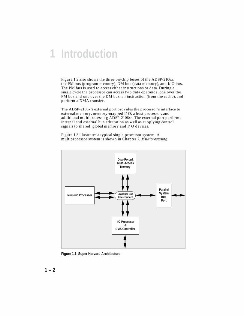
1 Introduction
1 – 2
Figure 1.2 also shows the three on-chip buses of the ADSP-2106x:the PM bus (program memory), DM bus (data memory), and I/O bus.The PM bus is used to access either instructions or data. During asingle cycle the processor can access two data operands, one over thePM bus and one over the DM bus, an instruction (from the cache), andperform a DMA transfer.
The ADSP-2106x’s external port provides the processor’s interface toexternal memory, memory-mapped I/O, a host processor, andadditional multiprocessing ADSP-2106xs. The external port performsinternal and external bus arbitration as well as supplying controlsignals to shared, global memory and I/O devices.
Figure 1.3 illustrates a typical single-processor system. Amultiprocessor system is shown in Chapter 7, Multiprocessing.
Figure 1.1 Super Harvard Architecture
Numeric Processor
I/O Processor&
DMA Controller
Dual-Ported,Multi-Access
Memory
ParallelSystem
BusPort
Crossbar BusInterconnect
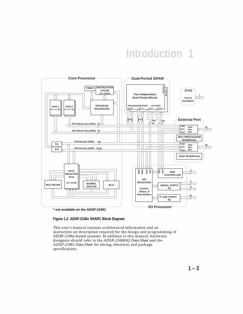
1Introduction
1 – 3
Figure 1.2 ADSP-2106x SHARC Block Diagram
This user’s manual contains architectural information and aninstruction set description required for the design and programming ofADSP-2106x-based systems. In addition to this manual, hardwaredesigners should refer to the ADSP-21060/62 Data Sheet and theADSP-21061 Data Sheet for timing, electrical, and packagespecifications.
AAAAAAAAAAAAAAAAAAAAAAAAAAAA
PM Address Bus (PMA) 24
DM Address Bus (DMA) 32
PM Data Bus (PMD)
DM Data Bus (DMD)
AAAAAA AAAAAA
AAAAAAAAAAAAAAAAAAAAAAAAAAAAAA
PROCESSOR PORT I/O PORT
SERIAL PORTS (2)
LINK PORTS (6)
INSTRUCTIONCACHE
32 x 48-Bit
DAG 28 x 4 x 24
DAG 18 x 4 x 32
TIMER
DMA CONTROLLER
Addr Bus Mux
32
48
AAAAAAAAAAAAAAAAAAAAAAAA
IOPREGISTERS
Control,Status, &
Data Buffers
6
6
36
4AAAAAAAAAAAAAAAAAAAAAAAAAAAAAAA
AAAAAAAAAAAAAAAAAAAAAAA
AA
ADDR DATA ADDR DATA
AA
7
A
A
JTAG
Bus Connect
(PX)
MULTIPLIER BARREL SHIFTER
ALU
AAAAAAAA
AAAAAAA
DATAREGISTER
FILE
16 x 40-Bit
AAAAAACore Processor
AAAAAAAAAADual-Ported SRAM
Two Independent,Dual-Ported Blocks
BL
OC
K 0
BL
OC
K 1
AAAAAAAAAAExternal Port
HOST INTERFACE
Test &Emulation
PROGRAMSEQUENCER
MULTIPROCESSORINTERFACE
48
IOD48
IOA17
AAAAAAAAA
IOD
EP
D
DM
D
PM
D
EP
A
IOA
AAAAAI/O Processor
AAAAAAA32/40
PMA
EPA
DMA
PMD
EPD
DMD
Data Bus Mux
AAAAAAAAAAAAA
*
* not available on the ADSP-21061
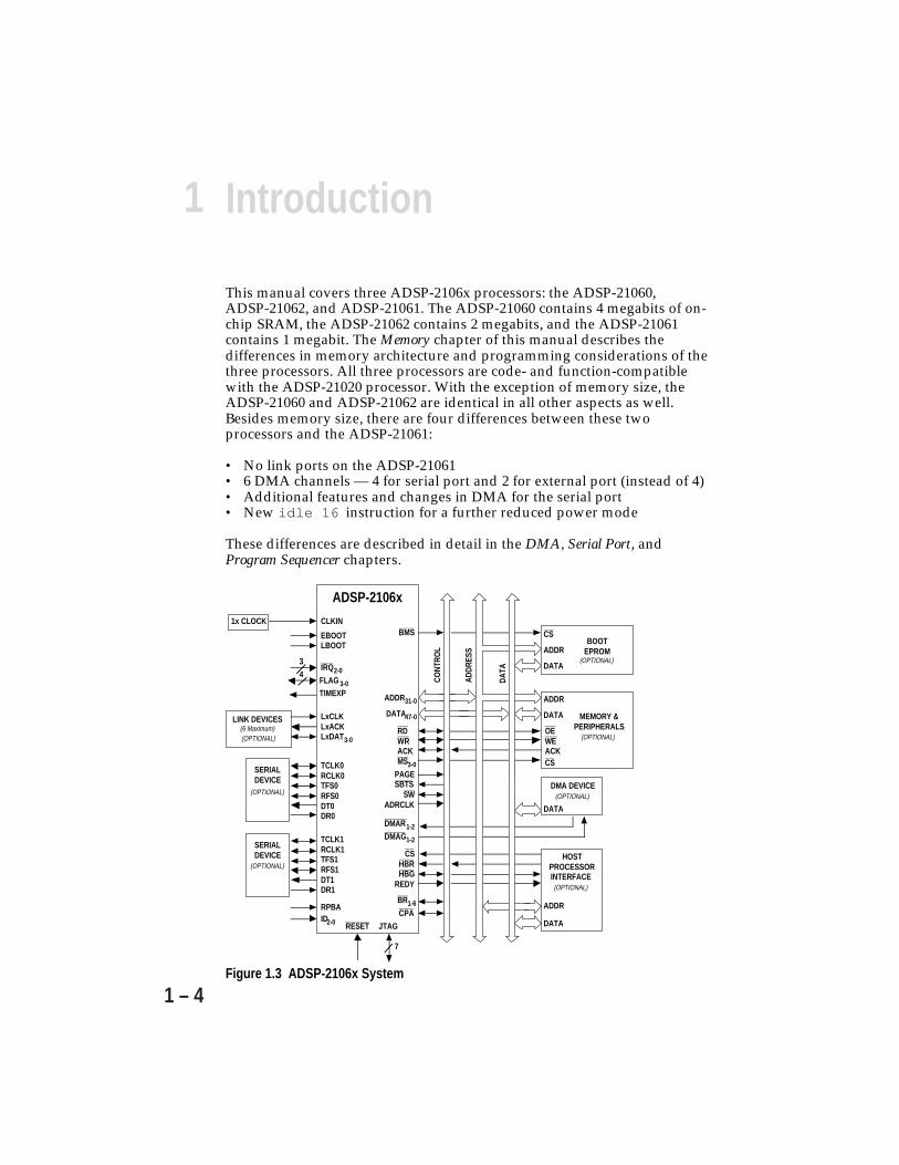
1 Introduction
1 – 4
This manual covers three ADSP-2106x processors: the ADSP-21060, ADSP-21062, and ADSP-21061. The ADSP-21060 contains 4 megabits of on-chip SRAM, the ADSP-21062 contains 2 megabits, and the ADSP-21061contains 1 megabit. The Memory chapter of this manual describes thedifferences in memory architecture and programming considerations of thethree processors. All three processors are code- and function-compatiblewith the ADSP-21020 processor. With the exception of memory size, theADSP-21060 and ADSP-21062 are identical in all other aspects as well.Besides memory size, there are four differences between these twoprocessors and the ADSP-21061:
• No link ports on the ADSP-21061• 6 DMA channels — 4 for serial port and 2 for external port (instead of 4)• Additional features and changes in DMA for the serial port• New idle 16 instruction for a further reduced power mode
These differences are described in detail in the DMA, Serial Port, andProgram Sequencer chapters.
Figure 1.3 ADSP-2106x System
ADDR
DATA
BOOT EPROM
CLKIN
RESET
IRQ2-0
EBOOTLBOOT
FLAG 3-0
DMAR1-2DMAG1-2
LxCLKLxACKLxDAT3-0
TIMEXP
RPBAID2-0
BMS
ADSP-2106x
ADDR
DATA
DATA
ADDR
DATA
ADDR31-0
DATA47-0
CS
MEMORY & PERIPHERALS
DMA DEVICE
(OPTIONAL)
LINK DEVICES(6 Maximum)(OPTIONAL)
(OPTIONAL)
SERIALDEVICE
(OPTIONAL)
(OPTIONAL)
(OPTIONAL)
JTAG
ADDR
ESS
DATA
CONT
ROL
7
4
3
SERIALDEVICE
(OPTIONAL)
HOSTPROCESSORINTERFACE
BR1-6
1x CLOCK
CPA
OEWEACKCS
RDWRACKMS3-0
PAGESBTS
SWADRCLK
CSHBRHBG
REDY
TCLK1RCLK1TFS1RFS1DT1DR1
TCLK0RCLK0TFS0RFS0DT0DR0

1Introduction
1 – 5
1.2 ADSP-21000 FAMILY FEATURES & BENEFITSThe ADSP-2106x SHARC processors belong to the ADSP-21000 Family offloating-point digital signal processors (DSPs). The ADSP-21000Family architecture further addresses the five central requirements forDSPs established in the ADSP-2100 Family of 16-bit fixed-point DSPs:
• Fast, flexible arithmetic computation units• Unconstrained data flow to and from the computation units• Extended precision and dynamic range in the computation units• Dual address generators• Efficient program sequencing
Fast, Flexible Arithmetic. The ADSP-21000 Family processors executeall instructions in a single cycle. They provide both fast cycle times anda complete set of arithmetic operations including Seed 1/X, Seed 1/√X,Min, Max, Clip, Shift, and Rotate, in addition to the traditionalmultiplication, addition, subtraction, and combined multiplication/addition. The processors are IEEE floating-point compatible and alloweither interrupt on arithmetic exception or latched status exceptionhandling.
Unconstrained Data Flow. The ADSP-2106x has an enhanced Harvardarchitecture combined with a 10-port data register file. In every cycle:
• Two operands can be read or written to or from the register file,• Two operands can be supplied to the ALU,• Two operands can be supplied to the multiplier, and• Two results can be received from the ALU and multiplier.
The processor’s 48-bit orthogonal instruction word supports fullyparallel data transfer and arithmetic operations in the same instruction.
40-Bit Extended Precision. The ADSP-21000 Family processors handle32-bit IEEE floating-point format, 32-bit integer and fractional formats(twos-complement and unsigned), and extended-precision 40-bit IEEEfloating-point format. The processors carry extended precisionthroughout their computation units, limiting intermediate datatruncation errors. When working with data on-chip, theextended-precision 32-bit mantissa can be transferred to and from allcomputation units. The 40-bit data bus may be extended off-chip ifdesired. The fixed-point formats have an 80-bit accumulator for true32-bit fixed-point computations.

1 Introduction
1 – 6
Dual Address Generators. The ADSP-21000 Family processors havetwo data address generators (DAGs) that provide immediate orindirect (pre- and post-modify) addressing. Modulus and bit-reverseoperations are supported with no constraints on data buffer placement.
Efficient Program Sequencing. In addition to zero-overhead loops, theADSP-21000 Family processors support single-cycle setup and exit forloops. Loops are both nestable (six levels in hardware) andinterruptable. The processors support both delayed and non-delayedbranches.
1.2.1 System-Level EnhancementsThe ADSP-21000 Family processors include several enhancements thatsimplify system development. The enhancements occur in three keyareas:
• Architectural features supporting high-level languages and operatingsystems
• IEEE 1149.1 JTAG serial scan path and on-chip emulation features• Support of IEEE floating-point formats
High Level Languages. The ADSP-21000 Family architecture hasseveral features that directly support high-level language compilersand operating systems:
• General purpose data and address register files• 32-bit native data types• Large address space• Pre- and post-modify addressing• Unconstrained circular data buffer placement• On-chip program, loop, and interrupt stacks
Additionally, the ADSP-21000 Family architecture is designedspecifically to support ANSI-standard Numerical C extensions—thefirst compiled language to support vector data types and operators fornumeric and signal processing.
Serial Scan and Emulation Features. The ADSP-21000 Familyprocessors support the IEEE standard P1149.1 Joint Test Action Group(JTAG) standard for system test. This standard defines a method forserially scanning the I/O status of each component in a system. TheJTAG serial port is also used by the ADSP-2106x EZ-ICE to gain accessto the processor’s on-chip emulation features.
1Introduction
1 – 7
IEEE Formats. The ADSP-21000 Family processors support IEEEfloating-point data formats. This means that algorithms developed onIEEE-compatible processors and workstations are portable acrossprocessors without concern for possible instability introduced bybiased rounding or inconsistent error handling.
1.2.2 Why Floating-Point DSP?A digital signal processor’s data format determines its ability to handlesignals of differing precision, dynamic range, and signal-to-noiseratios. However, ease-of-use and time-to-market considerations areoften equally important.
Precision. The number of bits of precision of A/D converters hascontinued to increase, and the trend is for both precision and samplingrates to increase.
Dynamic Range. Compression and decompression algorithms havetraditionally operated on signals of known bandwidth. Thesealgorithms were developed to behave regularly, to keep costs downand implementations easy. Increasingly, however, the trend inalgorithm development is not to constrain the regularity and dynamicrange of intermediate results. Adaptive filtering and imaging are twoapplications requiring wide dynamic range.
Signal-to-Noise Ratio. Radar, sonar and even commercial applicationslike speech recognition require wide dynamic range in order to discernselected signals from noisy environments.
Ease-of-Use. In general, 32-bit floating-point DSPs are easier to useand allow a quicker time-to-market than 16-bit fixed-point processors.The extent to which this is true depends on the floating-pointprocessor’s architecture. Consistency with IEEE workstationsimulations and the elimination of scaling are two clear ease-of-useadvantages. High-level language programmability, large addressspaces, and wide dynamic range allow system development time to bespent on algorithms and signal processing concerns rather thanassembly language coding, code paging, and error handling.
1 Introduction
1 – 8
1.3 ADSP-2106X ARCHITECTUREThe following sections summarize the features of the ADSP-2106xSHARC architecture. These features are described in greater detail insucceeding chapters.
1.3.1 Core ProcessorThe core processor of the ADSP-2106x consists of three computationunits, a program sequencer, two data address generators, timer,instruction cache, and data register file.
1.3.1.1 Computation UnitsThe ADSP-2106x core processor contains three independentcomputation units: an ALU, a multiplier with a fixed-pointaccumulator, and a shifter. For meeting a wide variety of processingneeds, the computation units process data in three formats: 32-bitfixed-point, 32-bit floating-point and 40-bit floating-point. The floating-point operations are single-precision IEEE-compatible. The 32-bitfloating-point format is the standard IEEE format, whereas the 40-bitIEEE extended-precision format has eight additional LSBs of mantissafor greater accuracy.
The ALU performs a standard set of arithmetic and logic operations inboth fixed-point and floating-point formats. The multiplier performsfloating-point and fixed-point multiplication as well as fixed-pointmultiply/add and multiply/subtract operations. The shifter performslogical and arithmetic shifts, bit manipulation, field deposit andextraction and exponent derivation operations on 32-bit operands.
The computation units perform single-cycle operations; there is nocomputation pipeline. The units are connected in parallel rather thanserially. The output of any unit may be the input of any unit on thenext cycle. In a multifunction computation, the ALU and multiplierperform independent, simultaneous operations.
1.3.1.2 Data Register FileA general-purpose data register file is used for transferring databetween the computation units and the data buses, and for storingintermediate results. The register file has two sets (primary andalternate) of sixteen registers each, for fast context switching. All of theregisters are 40 bits wide. The register file, combined with the coreprocessor’s Harvard architecture, allows unconstrained data flowbetween computation units and internal memory.

1Introduction
1 – 9
1.3.1.3 Program Sequencer & Data Address GeneratorsTwo dedicated address generators and a program sequencer supplyaddresses for memory accesses. Together the sequencer and dataaddress generators allow computational operations to execute withmaximum efficiency since the computation units can be devotedexclusively to processing data. With its instruction cache, theADSP-2106x can simultaneously fetch an instruction (from the cache)and access two data operands (from memory). The data addressgenerators implement circular data buffers in hardware.
The program sequencer supplies instruction addresses to programmemory. It controls loop iterations and evaluates conditionalinstructions. With an internal loop counter and loop stack, theADSP-2106x executes looped code with zero overhead. No explicitjump instructions are required to loop or to decrement and test thecounter.
The ADSP-2106x achieves its fast execution rate by means of pipelinedfetch, decode and execute cycles. If external memories are used, they areallowed more time to complete an access than if there were no decodecycle.
The data address generators (DAGs) provide memory addresses whendata is transferred between memory and registers. Dual data addressgenerators enable the processor to output simultaneous addresses fortwo operand reads or writes. DAG1 supplies 32-bit addresses to datamemory. DAG2 supplies 24-bit addresses to program memory forprogram memory data accesses.
Each DAG keeps track of up to eight address pointers, eight modifiersand eight length values. A pointer used for indirect addressing can bemodified by a value in a specified register, either before (pre-modify)or after (post-modify) the access. A length value may be associatedwith each pointer to perform automatic modulo addressing for circulardata buffers; the circular buffers can be located at arbitrary boundariesin memory. Each DAG register has an alternate register that can beactivated for fast context switching.
Circular buffers allow efficient implementation of delay lines and otherdata structures required in digital signal processing, and arecommonly used in digital filters and Fourier transforms. The DAGsautomatically handle address pointer wraparound, reducing overhead,increasing performance, and simplifying implementation.
1 Introduction
1 – 10
1.3.1.4 Instruction CacheThe program sequencer includes a 32-word instruction cache thatenables three-bus operation for fetching an instruction and two datavalues. The cache is selective—only instructions whose fetches conflictwith program memory data accesses are cached. This allows full-speedexecution of core, looped operations such as digital filtermultiply-accumulates and FFT butterfly processing.
1.3.1.5 InterruptsThe ADSP-2106x has four external hardware interrupts: threegeneral-purpose interrupts, IRQ2-0, and a special interrupt for reset.The processor also has internally generated interrupts for the timer,DMA controller operations, circular buffer overflow, stack overflows,arithmetic exceptions, multiprocessor vector interrupts, anduser-defined software interrupts.
For the general-purpose external interrupts and the internal timerinterrupt, the ADSP-2106x automatically stacks the arithmetic statusand mode (MODE1) registers in parallel with the interrupt servicing,allowing four nesting levels of very fast service for these interrupts.
1.3.1.6 TimerThe programmable interval timer provides periodic interruptgeneration. When enabled, the timer decrements a 32-bit count registerevery cycle. When this count register reaches zero, the ADSP-2106xgenerates an interrupt and asserts its TIMEXP output. The countregister is automatically reloaded from a 32-bit period register and thecount resumes immediately.
1.3.1.7 Core Processor BusesThe processor core has four buses: Program Memory Address, DataMemory Address, Program Memory Data, and Data Memory Data.On the ADSP-2106x processors, data memory stores data operandswhile program memory is used to store both instructions and data(filter coefficients, for example)—this allows dual data fetches, whenthe instruction is supplied by the cache.
1Introduction
1 – 11
The PM Address bus and DM Address bus are used to transfer theaddresses for instructions and data. The PM Data bus and DM Databus are used to transfer the data or instructions stored in each type ofmemory. The PM Address bus is 24 bits wide allowing access of up to16M words of mixed instructions and data. The PM Data bus is 48 bitswide to accommodate the 48-bit instruction width. Fixed-point andsingle-precision floating-point data is aligned to the upper 32 bits ofthe PM Data bus.
The DM Address bus is 32 bits wide allowing direct access of up to4G words of data. The DM Data bus is 40 bits wide. Fixed-point andsingle-precision floating-point data is aligned to the upper 32 bits ofthe DM Data bus. The DM Data bus provides a path for the contents ofany register in the processor to be transferred to any other register orto any data memory location in a single cycle. The data memoryaddress comes from one of two sources: an absolute value specified inthe instruction code (direct addressing) or the output of a data addressgenerator (indirect addressing).
1.3.1.8 Internal Data TransfersNearly every register in the core processor of the ADSP-2106x isclassified as a universal register. Instructions are provided fortransferring data between any two universal registers or between auniversal register and memory. This includes control registers andstatus registers, as well as the data registers in the register file.
The PX bus connect registers permit data to be passed between the48-bit PM Data bus and the 40-bit DM Data bus or between the 40-bitregister file and the PM Data bus. These registers contain hardware tohandle the 8-bit width difference.
1.3.1.9 Context SwitchingMany of the processor’s registers have alternate registers that can beactivated during interrupt servicing to facilitate a fast context switch.The data registers in the register file, the DAG registers, and themultiplier result register all have alternates. Registers active at resetare called primary registers, while the others are called alternate (orsecondary) registers. Control bits in a mode control register determinewhich set of registers is active at any particular time.
1 Introduction
1 – 12
1.3.1.10 Instruction SetThe ADSP-21000 Family instruction set provides a wide variety ofprogramming capabilities. Multifunction instructions enablecomputations in parallel with data transfers, as well as simultaneousmultiplier and ALU operations. The addressing power of theADSP-2106x gives you flexibility in moving data both internally andexternally. Every instruction can be executed in a single processorcycle. The ADSP-21000 Family assembly language uses an algebraicsyntax for ease of coding and readability. A comprehensive set ofdevelopment tools supports program development.
1.3.2 Dual-Ported Internal MemoryThe ADSP-21060 contains 4 megabits of on-chip SRAM, organized astwo blocks of 2 Mbits each, which can be configured for differentcombinations of code and data storage. The ADSP-21062 includes a2 Mbit SRAM, organized as two 1 Mbit blocks. Each memory block isdual-ported for single-cycle, independent accesses by the coreprocessor and I/O processor or DMA controller. The dual-portedmemory and separate on-chip buses allow two data transfers from thecore and one from I/O, all in a single cycle.
All of the memory can be accessed as 16-bit, 32-bit, or 48-bit words.On the ADSP-21060, the memory can be configured as a maximum of128K words of 32-bit data, 256K words of 16-bit data, 80K words of48-bit instructions (and 40-bit data), or combinations of different wordsizes up to 4 megabits. On the ADSP-21062, the memory can beconfigured as a maximum of 64K words of 32-bit data, 128K words of16-bit data, 40K words of 48-bit instructions (and 40-bit data), orcombinations of different word sizes up to 2 megabits. On the ADSP-21061, the memory can be configured as a maximum of 32K words of32-bit data, 64K words of 16-bit data, 16K words of 48-bit instructions(and 40-bit data), or combinations of different word sizes up to 1megabit.
A 16-bit floating-point storage format is supported which effectivelydoubles the amount of data that may be stored on chip. Conversionbetween the 32-bit floating-point and 16-bit floating-point formats isdone in a single instruction.
1Introduction
1 – 13
While each memory block can store combinations of code and data,accesses are most efficient when one block stores data, using theDM bus for transfers, and the other block stores instructions and data,using the PM bus for transfers. Using the DM bus and PM bus in thisway, with one dedicated to each memory block, assures single-cycleexecution with two data transfers. In this case, the instruction must beavailable in the cache. Single-cycle execution is also maintained whenone of the data operands is transferred to or from off-chip, via theADSP-2106x’s external port.
1.3.3 External Memory & Peripherals InterfaceThe ADSP-2106x’s external port provides the processor’s interface tooff-chip memory and peripherals. The 4-gigaword off-chip addressspace is included in the ADSP-2106x’s unified address space. Theseparate on-chip buses—for PM addresses, PM data, DM addresses,DM data, I/O addresses, and I/O data—are multiplexed at theexternal port to create an external system bus with a single 32-bitaddress bus and a single 48-bit data bus. External SRAM can be either16, 32, or 48 bits wide; the ADSP-2106x’s on-chip DMA controllerautomatically packs external data into the appropriate word width,either 48-bit instructions or 32-bit data.
Addressing of external memory devices is facilitated by on-chipdecoding of high-order address lines to generate memory bank selectsignals. Separate control lines are also generated for simplifiedaddressing of page-mode DRAM. The ADSP-2106x providesprogrammable memory wait states and external memory acknowledgecontrols to allow interfacing to DRAM and peripherals with variableaccess, hold, and disable time requirements.
1.3.4 Host Processor InterfaceThe ADSP-2106x’s host interface allows easy connection to standardmicroprocessor buses, both 16-bit and 32-bit, with little additionalhardware required. Asynchronous transfers at speeds up to the fullclock rate of the ADSP-2106x are supported. The host interface isaccessed through the ADSP-2106x’s external port and is memory-mapped into the unified address space. Four channels of DMA areavailable for the host interface; code and data transfers areaccomplished with low software overhead. The host can directly readand write the internal memory of the ADSP-2106x, and can access theDMA channel setup and mailbox registers. Vector interrupt support isprovided for efficient execution of host commands.
1 Introduction
1 – 14
1.3.5 MultiprocessingThe ADSP-2106x offers powerful features tailored to multiprocessingDSP systems. The unified address space allows direct interprocessoraccesses of each ADSP-2106x’s internal memory. Distributed busarbitration logic is included on-chip for simple, glueless connection ofsystems containing up to six ADSP-2106xs and a host processor.Master processor changeover incurs only one cycle of overhead. Busarbitration is selectable as either fixed or rotating priority. Processorbus lock allows indivisible read-modify-write sequences for semaphores.A vector interrupt capability is provided for interprocessor commands.Maximum throughput for interprocessor data transfer is240 Mbytes/sec over the link ports or external port. Broadcast writesallow simultaneous transmission of data to all ADSP-2106xs and canbe used to implement reflective semaphores.
1.3.6 I/O ProcessorThe ADSP-2106x’s I/O Processor (IOP) includes two serial ports, six4-bit link ports, and a DMA controller.
1.3.6.1 Serial PortsThe ADSP-2106x features two synchronous serial ports that provide aninexpensive interface to a wide variety of digital and mixed-signalperipheral devices. The serial ports can operate at the full clock rate ofthe processor, providing each with a maximum data rate of 40 Mbit/s.Independent transmit and receive functions provide greater flexibilityfor serial communications. Serial port data can be automaticallytransferred to and from on-chip memory via DMA. Each of the serialports offers a TDM multichannel mode.
The serial ports can operate with little-endian or big-endiantransmission formats, with word lengths selectable from 3 to 32 bits.They offer selectable synchronization and transmit modes as well asoptional µ-law or A-law companding. Serial port clocks and framesyncs can be internally or externally generated.

1Introduction
1 – 15
1.3.6.2 Link PortsThe ADSP-21062 and ADSP-21060 feature six 4-bit link ports thatprovide additional I/O capabilities. The link ports can be clocked twiceper cycle, allowing each to transfer 8 bits per cycle. Link port I/O isespecially useful for point-to-point interprocessor communication inmultiprocessing systems.
The link ports can operate independently and simultaneously, with amaximum data throughput of 240 Mbytes/s. Link port data is packedinto 32-bit or 48-bit words, and can be directly read by the coreprocessor or DMA-transferred to on-chip memory. Each link port hasits own double-buffered input and output registers.Clock/acknowledge handshaking controls link port transfers.Transfers are programmable as either transmit or receive.
There are no link ports on the ADSP-21061.
1.3.6.3 DMA ControllerThe ADSP-2106x’s on-chip DMA controller allows zero-overhead datatransfers without processor intervention. The DMA controller operatesindependently and invisibly to the processor core, allowing DMAoperations to occur while the core is simultaneously executing itsprogram. Both code and data can be downloaded to the ADSP-2106xusing DMA transfers.
DMA transfers can occur between the ADSP-2106x’s internal memoryand external memory, external peripherals, or a host processor. DMAtransfers can also occur between the ADSP-2106x’s internal memoryand its serial ports or link ports. DMA transfers between externalmemory and external peripheral devices are another option. Externalbus packing to 16, 32, or 48-bit words is automatically performedduring DMA transfers.
Ten channels of DMA are available on the ADSP-21060 andADSP-21062—two via the link ports, four via the serial ports, and fourvia the processor’s external port (for either host processor, otherADSP-2106xs, memory or I/O transfers). Four additional link portDMA channels are shared with serial port 1 and the external port.There are six channels of DMA available on the ADSP-21061—four viathe serial ports and two via the external port. Asynchronous off-chipperipherals can control two DMA channels using DMA Request/Grantlines (DMAR1-2 , DMAG1-2). Other DMA features include interruptgeneration upon completion of DMA transfers and DMA chaining forautomatic linked DMA transfers.
1 Introduction
1 – 16
The ten DMA channels of the ADSP-21060 and ADSP-21062 arenumbered as shown below:
DMA DataChannel# Buffer DescriptionDMA Channel 0 RX0 Serial Port 0 ReceiveDMA Channel 1 RX1 (or LBUF0) Serial Port 1 Receive (or Link Buffer 0)DMA Channel 2 TX0 Serial Port 0 TransmitDMA Channel 3 TX1 (or LBUF1) Serial Port 1 Transmit (or Link Buffer 1)DMA Channel 4 LBUF2 Link Buffer 2DMA Channel 5 LBUF3 Link Buffer 3DMA Channel 6 EPB0 (or LBUF4) Ext. Port FIFO Buffer 0 (or Link Buffer 4)DMA Channel 7 * EPB1 (or LBUF5) Ext. Port FIFO Buffer 1 (or Link Buffer 5)DMA Channel 8 * EPB2 Ext. Port FIFO Buffer 2DMA Channel 9 EPB3 Ext. Port FIFO Buffer 3
* DMAR1 and DMAG1 are handshake controls for DMA Channel 7.DMAR2 and DMAG2 are handshake controls for DMA Channel 8.
1.3.6.4 BootingThe internal memory of the ADSP-2106x can be booted at systempowerup from an 8-bit EPROM or a host processor. Additionally, theADSP-21060 and the ADSP-21062 can also be booted through one ofthe link ports. Selection of the boot source is controlled by the BMS,EBOOT, and LBOOT pins. Both 32-bit and 16-bit host processors canbe used for booting.
1.4 DEVELOPMENT TOOLSThe ADSP-2106x is supported with a complete set of software andhardware development tools, including an EZ-LAB EvaluationBoard, EZ-ICE In-Circuit Emulator, and development software. Thedevelopment software provides tools for programming and debuggingapplications in both assembly language and C. The EZ-ICE emulatorallows system integration and hardware/software debugging. Figure1.4 shows the process of developing an application using thedevelopment tools.
The development software includes an ANSI C Compiler. Thecompiler includes Numerical C extensions based on the work of theANSI NCEG committee (Numerical C Extensions Group).
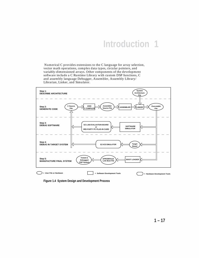
1Introduction
1 – 17
Numerical C provides extensions to the C language for array selection,vector math operations, complex data types, circular pointers, andvariably-dimensioned arrays. Other components of the developmentsoftware include a C Runtime Library with custom DSP functions, Cand assembly language Debugger, Assembler, Assembly Library/Librarian, Linker, and Simulator.
Step 1:DESCRIBE ARCHITECTURE
SystemArchitecture
File
Step 2:GENERATE CODE
LINKER ExecutableFile
AssemblerSource File ASSEMBLER
ANSIC COMPILER
C SourceFile
EZ-ICE EMULATOR
Step 3:DEBUG SOFTWARE
Step 4:DEBUG IN TARGET SYSTEM
EZ-LAB EVALUATION BOARDor
3RD-PARTY PC PLUG-IN CARD
SOFTWARE SIMULATOR
TargetBoard
Step 5:MANUFACTURE FINAL SYSTEM
BOOT LOADERTested &
DebuggedDSP System
= User File or Hardware = Software Development Tools = Hardware Development Tools
EPROM/Host/Link Boot File
Figure 1.4 System Design and Development Process
1 Introduction
1 – 18
The ADSP-2106x EZ-ICE Emulator uses the IEEE 1149.1 JTAG testaccess port of the ADSP-2106x processor to monitor and control thetarget board processor during emulation. The EZ-ICE provides full-speed emulation, allowing inspection and modification of memory,registers, and processor stacks. Non-intrusive in-circuit emulation isassured by the use of the processor’s JTAG interface—the emulatordoes not affect target system loading or timing.
Further details and ordering information are available in theADSP-21000 Family Hardware & Software Development Tools data sheet.This data sheet can be requested from any Analog Devices sales officeor distributor.
1.5 MESH MULTIPROCESSINGMesh multiprocessing is a parallel processing system architecture thatoffers high throughput, system flexibility, and software simplicity. TheADSP-21060 and ADSP-21062 SHARC processors include featureswhich specifically support this system architecture. Meshmultiprocessing systems are suited to a wide variety of applicationsincluding wide-area airborne radar systems, interactive medicalimaging, virtual reality, high-speed engineering simulations, neuralnetworks, and solutions of large systems of linear equations.
1.6 ADDITIONAL LITERATUREThe following publications can be ordered from any Analog Devicessales office.
ADSP-21060/62 SHARC Data SheetADSP-21061 SHARC Data SheetADSP-21000 Family Hardware & Software Development Tools Data SheetADSP-21000 Family Assembler Tools & Simulator ManualADSP-21000 Family C Tools ManualADSP-21000 Family C Runtime Library ManualADSP-21000 Family Applications Handbook, Vol. 1
2Computation Units
2.1 OVERVIEWThe computation units of the ADSP-2106x provide the numeric processingpower for performing DSP algorithms. The ADSP-2106x contains threecomputation units: an arithmetic/logic unit (ALU), a multiplier and ashifter. Both fixed-point and floating-point operations are supported bythe processor. Each computation unit executes instructions in a singlecycle.
The ALU performs a standard set of arithmetic and logic operations inboth fixed-point and floating-point formats. The multiplier performsfloating-point and fixed-point multiplication as well as fixed-pointmultiply/add and multiply/subtract operations. The shifter performslogical and arithmetic shifts, bit manipulation, field deposit and extractionoperations on 32-bit operands and can derive exponents as well.
The computation units are architecturally arranged in parallel, as shownin Figure 2.1 on the next page. The output of any computation unit may bethe input of any computation unit on the next cycle. The computationunits input data from and output data to a 10-port register file thatconsists of sixteen primary registers and sixteen alternate registers. Theregister file is accessible to the ADSP-2106x program and data memorydata buses for transferring data between the computation units andexternal memory or other parts of the processor.
The individual registers of the register file are prefixed with an “F” whenused in floating-point computations (in assembly language source code).The registers are prefixed with an “R” when used in fixed-pointcomputations. The following instructions, for example, use the sameregisters:
F0=F1 * F2; floating-point multiplyR0=R1 * R2; fixed-point multiply
The F and R prefixes do not affect the 32-bit (or 40-bit) data transfer; theyonly determine how the ALU, multiplier, or shifter treat the data. The F orR may be either uppercase or lowercase; the assembler is case-insensitive.
2 – 1
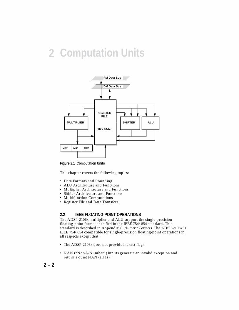
2 Computation Units
2 – 2
This chapter covers the following topics:
• Data Formats and Rounding• ALU Architecture and Functions• Multiplier Architecture and Functions• Shifter Architecture and Functions• Multifunction Computations• Register File and Data Transfers
2.2 IEEE FLOATING-POINT OPERATIONSThe ADSP-2106x multiplier and ALU support the single-precisionfloating-point format specified in the IEEE 754/854 standard. Thisstandard is described in Appendix C, Numeric Formats. The ADSP-2106x isIEEE 754/854 compatible for single-precision floating-point operations inall respects except that:
• The ADSP-2106x does not provide inexact flags.
• NAN (“Not-A-Number”) inputs generate an invalid exception andreturn a quiet NAN (all 1s).
Figure 2.1 Computation Units
REGISTERFILE
MULTIPLIER ALUSHIFTER
16 x 40-bit
PM Data Bus
DM Data Bus
MR0MR1MR2

2Computation Units
2 – 3
• Denormal operands are flushed to zero when input to a computation unitand do not generate an underflow exception. Any denormal orunderflow result from an arithmetic operation is flushed to zero and anunderflow exception is generated.
• Round-to-nearest and round-toward-zero modes are supported.Rounding to +Infinity and rounding to –Infinity are not supported.
In addition, the ADSP-2106x supports a 40-bit extended precision floating-point mode, which has eight additional LSBs of the mantissa and iscompliant with the 754/854 standards; however, results in this format aremore precise than the IEEE single-precision standard specifies.
2.2.1 Extended Floating-Point PrecisionFloating-point data can be either 32 or 40 bits wide on the ADSP-2106x.Extended precision floating-point format (8 bits of exponent and 32 bits ofmantissa) is selected if the RND32 bit in the MODE1 register is cleared (0).If this bit is set (1), then normal IEEE precision is used (8 bits exponent and24 bits of mantissa). In this case, the computation unit sets the eight LSBs offloating-point inputs to zeros before performing the operation. Themantissa of a result is rounded to 23 bits (not including the hidden bit) andthe 8 LSBs of the 40-bit result are set to zeros to form a 32-bit number that isequivalent to the IEEE standard result.
2.2.2 Short Word Floating-Point FormatThe ADSP-2106x supports a 16-bit floating-point data type and providesconversion instructions for it. The short float data format has an 11-bitmantissa with a four-bit exponent plus sign bit. The 16-bit floating-pointnumbers reside in the lower 16 bits of the 32-bit floating-point field.
Two shifter instructions, FPACK and FUNPACK, perform the packingand unpacking conversions between 32-bit floating-point words and 16-bitfloating-point words. The FPACK instruction converts a 32-bit IEEEfloating-point number to a 16-bit floating-point number. FUNPACKconverts the 16-bit floating-point numbers back to 32-bit IEEE floating-point. Each instruction executes in a single cycle.
The short float type supports gradual underflow. This method sacrificesprecision for dynamic range. When packing a number which would haveunderflowed, the exponent is set to zero and the mantissa (including“hidden” 1) is right-shifted the appropriate amount. The packed result is adenormal which can be unpacked into a normal IEEE floating-pointnumber.

2 Computation Units
2 – 4
2.2.3 Floating-Point ExceptionsThe multiplier and ALU each provide exception information whenexecuting floating-point operations. Each unit updates overflow,underflow and invalid operation flags in the arithmetic status (ASTAT)register and in the sticky status (STKY) register. An underflow, overflowor invalid operation from any unit also generates a maskable interrupt.Thus, there are three ways to handle floating-point exceptions:
• Interrupts. The exception condition is handled immediately in aninterrupt service routine. You would use this method if it was importantto correct all exceptions as they happen.
• ASTAT register. The exception flags in the ASTAT register pertainingto a particular arithmetic operation are tested after the operation isperformed. You would use this method to monitor a particular floating-point operation.
• STKY register. Exception flags in the STKY register are examined at theend of a series of operations. If any flags are set, some of the results areincorrect. You would use this method if exception handling was notcritical.
2.3 FIXED-POINT OPERATIONSFixed-point numbers are always represented in 32 bits and are left-justified (occupy the 32 MSBs) in the 40-bit data fields of the ADSP-2106x.They may be treated as fractional or integer numbers and as unsigned ortwos-complement. Each computation unit has its own limitations on howthese formats may be mixed for a given operation. The computation unitsread 32-bit operands from 40-bit registers, ignoring the 8 LSBs, and write32-bit results, zeroing the 8 LSBs.
2.4 ROUNDINGTwo modes of rounding are supported in the ADSP-2106x: round-toward-zero and round-toward-nearest. The rounding modes follow the IEEE 754standard definitions, which are briefly stated as follows:
Round-Toward-Zero. If the result before rounding is not exactlyrepresentable in the destination format, the rounded result is that numberwhich is nearer to zero. This is equivalent to truncation.

2Computation Units
2 – 5
Round-Toward-Nearest. If the result before rounding is not exactlyrepresentable in the destination format, the rounded result is that numberwhich is nearer to the result before rounding. If the result before rounding isexactly halfway between two numbers in the destination format (differing byan LSB), the rounded result is that number which has an LSB equal to zero.Statistically, rounding up occurs as often as rounding down, so there is nolarge sample bias. Because the maximum floating-point value is one LSB lessthan the value that represents Infinity, a result that is halfway between themaximum floating-point value and Infinity rounds to Infinity in this mode.
The rounding mode for all ALU operations and for floating-point multiplieroperations is determined by the TRUNC bit in the MODE1 register. If theTRUNC bit is set, the round-to-zero mode is selected; otherwise, the round-to-nearest mode is used.
For fixed-point multiplier operations on fractional data, the same tworounding modes are supported, but only the round-to-nearest operation isactually performed by the multiplier. Because the multiplier has a local resultregister for fixed-point operations, rounding-to-zero is accomplishedimplicitly by reading only the upper bits of the result and discarding thelower bits.
2.5 ALUThe ALU performs arithmetic operations on fixed-point or floating-point dataand logical operations on fixed-point data. ALU fixed-point instructionsoperate on 32-bit fixed-point operands and output 32-bit fixed-point results.ALU floating-point instructions operate on 32-bit or 40-bit floating-pointoperands and output 32-bit or 40-bit floating-point results.
ALU instructions include:
• Floating-point addition, subtraction, add/subtract, average• Fixed-point addition, subtraction, add/subtract, average• Floating-point manipulation: binary log, scale, mantissa• Fixed-point add with carry, subtract with borrow, increment, decrement• Logical AND, OR, XOR, NOT• Functions: Absolute value, pass, min, max, clip, compare• Format conversion• Reciprocal and reciprocal square root primitives
Dual add/subtract and parallel ALU and multiplier operations are describedunder “Multifunction Computations,” later in this chapter.
2 Computation Units
2 – 6
2.5.1 ALU OperationThe ALU takes one or two input operands, called the X input and the Yinput, which can be any data registers in the register file. It usually returnsone result; in add/subtract operations it returns two results, and incompare operations it returns no result (only flags are updated). ALUresults can be returned to any location in the register file.
Input operands are transferred from the register file during the first half ofthe cycle. Results are transferred to the register file during the second halfof the cycle. Thus the ALU can read and write the same register filelocation in a single cycle.
If the ALU operation is fixed-point, the X input and Y input are eachtreated as a 32-bit fixed-point operand. The upper 32 bits from the sourcelocation in the register file are transferred. For fixed-point operations, theresult(s) are always 32-bit fixed-point values. Some floating-pointoperations (LOGB, MANT and FIX) can also yield fixed-point results.Fixed-point results are transferred to the upper 32 bits of register file. Thelower eight bits of the register file destination are cleared.
The format of fixed-point operands and results depends on the operation.In most arithmetic operations, there is no need to distinguish betweeninteger and fractional formats. Fixed-point inputs to operations such asscaling a floating-point value are treated as integers. For purposes ofdetermining status such as overflow, fixed-point arithmetic operands andresults are treated as twos-complement numbers.
2.5.2 ALU Operating ModesThe ALU is affected by three bits in the MODE1 register; the ALUsaturation bit affects ALU operations that yield fixed-point results, and therounding mode and rounding boundary bits affect floating-pointoperations in both the ALU and multiplier.
MODE1Bit Name Function13 ALUSAT 1=Enable ALU saturation (full scale in fixed-point)
0=Disable ALU saturation15 TRUNC 1=Truncation; 0=Round to nearest16 RND32 1=Round to 32 bits; 0=Round to 40 bits
2Computation Units
2 – 7
2.5.2.1 Saturation ModeIn saturation mode, all positive fixed-point overflows cause the maximumpositive fixed-point number (0x7FFF FFFF) to be returned, and allnegative overflows cause the maximum negative number (0x8000 0000) tobe returned. If the ALUSAT bit is set, fixed-point results that overflow aresaturated. If the ALUSAT bit is cleared, fixed-point results that overfloware not saturated; the upper 32 bits of the result are returned unaltered.The ALU overflow flag reflects the ALU result before saturation.
2.5.2.2 Floating-Point Rounding ModesThe ALU supports two IEEE rounding modes. If the TRUNC bit is set, theALU rounds a result to zero (truncation). If the TRUNC bit is cleared, theALU rounds to nearest.
2.5.2.3 Floating-Point Rounding BoundaryThe results of floating-point ALU operations can be either 32-bit or 40-bitfloating-point data on the ADSP-2106x. If the RND32 bit is set, the eightLSBs of each input operand are flushed to zeros before the ALU operationis performed (except for the RND operation), and ALU floating-pointresults are output in the 32-bit IEEE format. The lower eight bits of theresult are cleared. If the RND32 bit is cleared, the ALU inputs 40-bitoperands unchanged and outputs 40-bit results from floating-pointoperations, and all 40 bits are written to the specified register file location.
In fixed-point to floating-point conversion, the rounding boundary isalways 40 bits even if the RND32 bit is set.
2.5.3 ALU Status FlagsThe ALU updates seven status flags in the ASTAT register, shown below,at the end of each operation. The states of these flags reflect the result ofthe most recent ALU operation. The ALU updates the CompareAccumulation bits in ASTAT at the end of every Compare operation. TheALU also updates four “sticky” status flags in the STKY register. Once set,a sticky flag remains high until explicitly cleared.
ASTATBit Name Definition0 AZ ALU result zero or floating-point underflow1 AV ALU overflow2 AN ALU result negative3 AC ALU fixed-point carry4 AS ALU X input sign (ABS, MANT operations)5 AI ALU floating-point invalid operation10 AF Last ALU operation was a floating-point operation31-24 CACC Compare Accumulation register (results of last 8 compare
operations)

2 Computation Units
2 – 8
STKYBit Name Definition0 AUS ALU floating-point underflow1 AVS ALU floating-point overflow2 AOS ALU fixed-point overflow5 AIS ALU floating-point invalid operation
Flag update occurs at the end of the cycle in which the status is generatedand is available on the next cycle. If a program writes the ASTAT registeror STKY register explicitly in the same cycle that the ALU is performingan operation, the explicit write to ASTAT or STKY supersedes any flagupdate from the ALU operation.
2.5.3.1 ALU Zero Flag (AZ)The zero flag is determined for all fixed-point and floating-point ALUoperations. AZ is set whenever the result of an ALU operation is zero.AZ also signifies floating-point underflow; see the next section. It isotherwise cleared.
2.5.3.2 ALU Underflow Flag (AZ, AUS)Underflow is determined for all ALU operations that return a floating-point result and for floating-point to fixed-point conversion. AUS is setwhenever the result of an ALU operation is smaller than the smallestnumber representable in the output format. AZ is set whenever afloating-point result is smaller than the smallest number representable inthe output format.
2.5.3.3 ALU Negative Flag (AN)The negative flag is determined for all ALU operations. It is set wheneverthe result of an ALU operation is negative. It is otherwise cleared.
2.5.3.4 ALU Overflow Flag (AV, AOS, AVS)Overflow is determined for all fixed-point and floating-point ALUoperations. For fixed-point results, AV and AOS are set whenever theXOR of the two most significant bits is a 1; otherwise AV is cleared. Forfloating-point results AV and AVS are set whenever the post-roundedresult overflows (unbiased exponent > 127); otherwise AV is cleared.
2Computation Units
2 – 9
2.5.3.5 ALU Fixed-Point Carry Flag (AC)The carry flag is determined for all fixed-point ALU operations. Forfixed-point arithmetic operations, AC is set if there is a carry out of mostsignificant bit of the result, and is otherwise cleared. AC is cleared forfixed-point logic, PASS, MIN, MAX, COMP, ABS, and CLIP operations.The ALU reads the AC flag in fixed-point addition with carry andfixed-point subtraction with carry operations.
2.5.3.6 ALU Sign Flag (AS)The sign flag is determined for only the fixed-point and floating-pointABS operations and the MANT operation. AS is set if the input operand isnegative. It is otherwise cleared. The ALU clears AS for all operationsother than ABS and MANT operations; this is different from the operationof ADSP-2100 family processors, which do not update the AS flag onoperations other than ABS.
2.5.3.7 ALU Invalid Flag (AI)The invalid flag is determined for all floating-point ALU operations. AI and AIS are set whenever
• an input operand is a NAN• an addition of opposite-signed Infinities is attempted• a subtraction of like-signed Infinities is attempted• when saturation mode is not set, a floating-point to fixed-point
conversion results in an overflow or operates on an Infinity.
AI is otherwise cleared.
2.5.3.8 ALU Floating-Point Flag (AF)AF is determined for all fixed-point and floating-point ALU operations. Itis set if the last operation was a floating-point operation; it is otherwisecleared.
2.5.3.9 Compare AccumulationBits 31-24 in the ASTAT register store the flag results of up to eight ALUcompare operations. These bits form a right-shift register. When an ALUcompare operation is executed, the eight bits are shifted toward the LSB(bit 24 is lost). The MSB, bit 31, is then written with the result of thecompare operation. If the X operand is greater than the Y operand in thecompare instruction, bit 31 is set; it is cleared otherwise. The accumulatedcompare flags can be used to implement 2- and 3-dimensional clippingoperations for graphics applications.

2 Computation Units
2 – 10
2.5.4 ALU Instruction Summary
Fixed-point: AZ AV AN AC AS AI AF CACC AUS AVS AOS AISc Rn = Rx + Ry * * * * 0 0 0 – – – ** –c Rn = Rx – Ry * * * * 0 0 0 – – – ** –c Rn = Rx + Ry + CI * * * * 0 0 0 – – – ** –c Rn = Rx – Ry + CI – 1 * * * * 0 0 0 – – – ** –
Rn = (Rx + Ry)/2 * 0 * * 0 0 0 – – – – –COMP(Rx, Ry) * 0 * 0 0 0 0 * – – – –Rn = Rx + CI * * * * 0 0 0 – – – ** –Rn = Rx + CI – 1 * * * * 0 0 0 – – – ** –Rn = Rx + 1 * * * * 0 0 0 – – – ** –Rn = Rx – 1 * * * * 0 0 0 – – – ** –
c Rn = –Rx * * * * 0 0 0 – – – ** –c Rn = ABS Rx * * 0 0 * 0 0 – – – ** –
Rn = PASS Rx * 0 * 0 0 0 0 – – – – –c Rn = Rx AND Ry * 0 * 0 0 0 0 – – – – –c Rn = Rx OR Ry * 0 * 0 0 0 0 – – – – –c Rn = Rx XOR Ry * 0 * 0 0 0 0 – – – – –c Rn = NOT Rx * 0 * 0 0 0 0 – – – – –
Rn = MIN(Rx, Ry) * 0 * 0 0 0 0 – – – – –Rn = MAX(Rx, Ry) * 0 * 0 0 0 0 – – – – –Rn = CLIP Rx BY Ry * 0 * 0 0 0 0 – – – – –
Floating–point:Fn = Fx + Fy * * * 0 0 * 1 – ** ** – **Fn = Fx – Fy * * * 0 0 * 1 – ** ** – **Fn = ABS (Fx + Fy) * * 0 0 0 * 1 – ** ** – **Fn = ABS (Fx – Fy) * * 0 0 0 * 1 – ** ** – **Fn = (Fx + Fy)/2 * 0 * 0 0 * 1 – ** – – **COMP(Fx, Fy) * 0 * 0 0 * 1 * – – – **Fn = –Fx * * * 0 0 * 1 – – ** – **Fn = ABS Fx * * 0 0 * * 1 – – ** – **Fn = PASS Fx * 0 * 0 0 * 1 – – – – **Fn = RND Fx * * * 0 0 * 1 – – ** – **Fn = SCALB Fx BY Ry * * * 0 0 * 1 – ** ** – **Rn = MANT Fx * * 0 0 * * 1 – – ** – **Rn = LOGB Fx * * * 0 0 * 1 – – ** – **Rn = FIX Fx BY Ry * * * 0 0 * 1 – ** ** – **Rn = FIX Fx * * * 0 0 * 1 – ** ** – **Fn = FLOAT Rx BY Ry * * * 0 0 0 1 – ** ** – –Fn = FLOAT Rx * 0 * 0 0 0 1 – – – – –Fn = RECIPS Fx * * * 0 0 * 1 – ** ** – **Fn = RSQRTS Fx * * * 0 0 * 1 – – ** – **Fn = Fx COPYSIGN Fy * 0 * 0 0 * 1 – – – – **Fn = MIN(Fx, Fy) * 0 * 0 0 * 1 – – – – **Fn = MAX(Fx, Fy) * 0 * 0 0 * 1 – – – – **Fn = CLIP Fx BY Fy * 0 * 0 0 * 1 – – – – **
Rn, Rx, Ry = Any register file location; treated as fixed-pointFn, Fx, Fy = Any register file location; treated as floating-pointc = ADSP-21xx-compatible instruction
* set or cleared, depending on results of instruction** may be set (but not cleared), depending on results of instruction– no effect
Instruction ASTAT Status Flags STKY Status Flags

2Computation Units
2 – 11
2.6 MULTIPLIERThe multiplier performs fixed-point or floating-point multiplication and fixed-point multiply/accumulate operations. Fixed-point multiply/accumulates maybe performed with either cumulative addition or cumulative subtraction.Floating-point multiply/accumulates can be accomplished through paralleloperation of the ALU and multiplier, using multifunction instructions. See“Multifunction Computations” later in this chapter.
Multiplier floating-point instructions operate on 32-bit or 40-bit floating-pointoperands and output 32-bit or 40-bit floating-point results. Multiplier fixed-pointinstructions operate on 32-bit fixed-point data and produce 80-bit results. Inputsare treated as fractional or integer, unsigned or twos-complement.
Multiplier instructions include:
• Floating-point multiplication• Fixed-point multiplication• Fixed-point multiply/accumulate with addition, rounding optional• Fixed-point multiply/accumulate with subtraction, rounding optional• Rounding result register• Saturating result register• Clearing result register
2.6.1 Multiplier OperationThe multiplier takes two input operands, called the X input and the Y input,which can be any data registers in the register file. Fixed-point operations canaccumulate fixed-point results in either of two local multiplier result registers(MR) or write results back to the register file. Results stored in the MR registerscan also be rounded or saturated in separate operations. Floating-pointoperations yield floating-point results, which are always written directly backto the register file.
Input operands are transferred during the first half of the cycle. Results aretransferred during the second half of the cycle. Thus the multiplier can readand write the same register file location in a single cycle.
If the multiplier operation is fixed-point, inputs taken from the register file areread from the upper 32 bits of the source location. Fixed-point operands may betreated as both in integer format or both in fractional format. The format of theresult is the same as the format of the inputs. Each fixed-point operand may betreated as either an unsigned or a twos-complement number. If both inputs arefractional and signed, the multiplier automatically shifts the result left one bit toremove the redundant sign bit. The input data type is specified within themultiplier instruction.
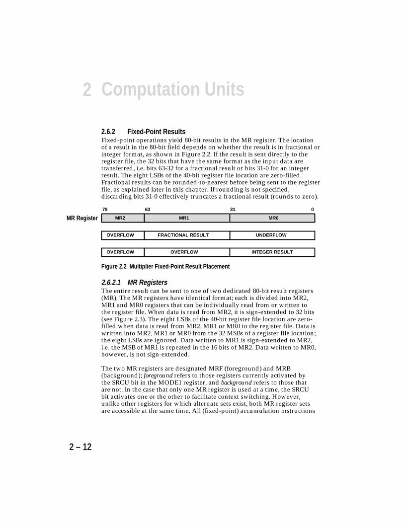
2 Computation Units
2 – 12
2.6.2 Fixed-Point ResultsFixed-point operations yield 80-bit results in the MR register. The locationof a result in the 80-bit field depends on whether the result is in fractional orinteger format, as shown in Figure 2.2. If the result is sent directly to theregister file, the 32 bits that have the same format as the input data aretransferred, i.e. bits 63-32 for a fractional result or bits 31-0 for an integerresult. The eight LSBs of the 40-bit register file location are zero-filled.Fractional results can be rounded-to-nearest before being sent to the registerfile, as explained later in this chapter. If rounding is not specified,discarding bits 31-0 effectively truncates a fractional result (rounds to zero).
0316379
FRACTIONAL RESULT
INTEGER RESULTOVERFLOW
OVERFLOW UNDERFLOW
OVERFLOW
MR2 MR1 MR0
Figure 2.2 Multiplier Fixed-Point Result Placement
2.6.2.1 MR RegistersThe entire result can be sent to one of two dedicated 80-bit result registers(MR). The MR registers have identical format; each is divided into MR2,MR1 and MR0 registers that can be individually read from or written tothe register file. When data is read from MR2, it is sign-extended to 32 bits(see Figure 2.3). The eight LSBs of the 40-bit register file location are zero-filled when data is read from MR2, MR1 or MR0 to the register file. Data iswritten into MR2, MR1 or MR0 from the 32 MSBs of a register file location;the eight LSBs are ignored. Data written to MR1 is sign-extended to MR2,i.e. the MSB of MR1 is repeated in the 16 bits of MR2. Data written to MR0,however, is not sign-extended.
The two MR registers are designated MRF (foreground) and MRB(background); foreground refers to those registers currently activated bythe SRCU bit in the MODE1 register, and background refers to those thatare not. In the case that only one MR register is used at a time, the SRCUbit activates one or the other to facilitate context switching. However,unlike other registers for which alternate sets exist, both MR register setsare accessible at the same time. All (fixed-point) accumulation instructions
MR Register
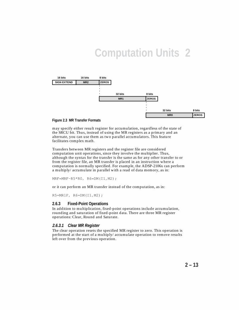
2Computation Units
2 – 13
16 bits
MR2
MR1
MR0
SIGN EXTEND
8 bits
ZEROS
ZEROS
ZEROS
16 bits
8 bits32 bits
8 bits32 bits
Figure 2.3 MR Transfer Formats
may specify either result register for accumulation, regardless of the state ofthe SRCU bit. Thus, instead of using the MR registers as a primary and analternate, you can use them as two parallel accumulators. This featurefacilitates complex math.
Transfers between MR registers and the register file are consideredcomputation unit operations, since they involve the multiplier. Thus,although the syntax for the transfer is the same as for any other transfer to orfrom the register file, an MR transfer is placed in an instruction where acomputation is normally specified. For example, the ADSP-2106x can performa multiply/accumulate in parallel with a read of data memory, as in:
MRF=MRF-R5*R0, R6=DM(I1,M2);
or it can perform an MR transfer instead of the computation, as in:
R5=MR1F, R6=DM(I1,M2);
2.6.3 Fixed-Point OperationsIn addition to multiplication, fixed-point operations include accumulation,rounding and saturation of fixed-point data. There are three MR registeroperations: Clear, Round and Saturate.
2.6.3.1 Clear MR RegisterThe clear operation resets the specified MR register to zero. This operation isperformed at the start of a multiply/accumulate operation to remove resultsleft over from the previous operation.

2 Computation Units
2 – 14
2.6.3.2 Round MR RegisterRounding of a fixed-point result occurs either as part of a multiply ormultiply/accumulate operation or as an explicit operation on the MRregister. The rounding operation applies only to fractional results (integerresults are not affected) and rounds the 80-bit MR value to nearest at bit32, i.e. at the MR1-MR0 boundary. The rounded result in MR1 can be senteither to the register file or back to the same MR register. To round afractional result to zero (truncation) instead of to nearest, you wouldsimply transfer the unrounded result from MR1, discarding the lower 32bits in MR0.
2.6.3.3 Saturate MR Register On OverflowThe saturate operation sets MR to a maximum value if the MR value hasoverflowed. Overflow occurs when the MR value is greater than themaximum value for the data format (unsigned or twos-complement andinteger or fractional) that is specified in the saturate instruction. There aresix possible maximum values (shown in hexadecimal):
MR2 MR1 MR0Maximum twos-complement fractional number0000 7FFF FFFF FFFF FFFF positiveFFFF 8000 0000 0000 0000 negative
Maximum twos-complement integer number0000 0000 0000 7FFF FFFF positiveFFFF FFFF FFFF 8000 0000 negative
Maximum unsigned fractional number0000 FFFF FFFF FFFF FFFF
Maximum unsigned integer number0000 0000 0000 FFFF FFFF
The result from MR saturation can be sent either to the register file or backto the same MR register.
2Computation Units
2 – 15
2.6.4 Floating-Point Operating ModesThe multiplier is affected by two mode status bits in the MODE1 register:the rounding mode and rounding boundary bits, which affect operationsin both the multiplier and the ALU.
MODE1Bit Name Function15 TRUNC 1=Truncation; 0=Round to nearest16 RND32 1=Round to 32 bits; 0=Round to 40 bits
2.6.4.1 Floating-Point Rounding ModesThe multiplier supports two IEEE rounding modes for floating-pointoperations. If the TRUNC bit is set, the multiplier rounds a floating-pointresult to zero (truncation). If the TRUNC bit is cleared, the multiplierrounds to nearest.
2.6.4.2 Floating-Point Rounding BoundaryFloating-point multiplier inputs and results can be either 32-bit or 40-bitfloating-point data on the ADSP-2106x. If the RND32 bit is set, the eightLSBs of each input operand are flushed to zeros before multiplication, andfloating-point results are output in the 32-bit IEEE format, with the lowereight bits of the 40-bit register file location cleared. The mantissa of theresult is rounded to 23 bits (not including the hidden bit). If the RND32 bitis cleared, the multiplier inputs full 40-bit values from the register file andoutputs results in the 40-bit extended IEEE format, with the mantissarounded to 31 bits not including the hidden bit.
2.6.5 Multiplier Status FlagsThe multiplier updates four status flags at the end of each operation. Allof these flags appear in the ASTAT register. The states of these flags reflectthe result of the most recent multiplier operation. The multiplier alsoupdates four “sticky” status flags in the STKY register. Once set, a stickyflag remains high until explicitly cleared.
ASTATBit Name Definition6 MN Multiplier result negative7 MV Multiplier overflow8 MU Multiplier underflow9 MI Multiplier floating-point invalid operation
2 Computation Units
2 – 16
STKYBit Name Definition6 MOS Multiplier fixed-point overflow7 MVS Multiplier floating-point overflow8 MUS Multiplier underflow9 MIS Multiplier floating-point invalid operation
Flag update occurs at the end of the cycle in which the status is generatedand is available on the next cycle. If a program writes the ASTAT registeror STKY register explicitly in the same cycle that the multiplier isperforming an operation, the explicit write to ASTAT or STKY supersedesany flag update from the multiplier operation.
2.6.5.1 Multiplier Underflow Flag (MU)Underflow is determined for all fixed-point and floating-point multiplieroperations. It is set whenever the result of a multiplier operation is smallerthan the smallest number representable in the output format. It isotherwise cleared.
For floating-point results, MU and MUS are set whenever the post-rounded result underflows (unbiased exponent < –126). Denormaloperands are treated as Zeros, therefore they never cause underflows.
For fixed-point results, MU and MUS depend on the data format and areset under the following conditions:
Twos-complement:Fractional: upper 48 bits all zeros or all ones, lower 32 bits not all zerosInteger: not possible
Unsigned:Fractional: upper 48 bits all zeros, lower 32 bits not all zerosInteger: not possible
If the fixed-point result is sent to an MR register, the underflowed portionof the result is available in MR0 (fractional result only).
2Computation Units
2 – 17
2.6.5.2 Multiplier Negative Flag (MN)The negative flag is determined for all multiplier operations. MN is setwhenever the result of a multiplier operation is negative. It is otherwise cleared.
2.6.5.3 Multiplier Overflow Flag (MV)Overflow is determined for all fixed-point and floating-point multiplieroperations.
For floating-point results, MV and MVS are set whenever the post-roundedresult overflows (unbiased exponent > 127).
For fixed-point results, MV and MOS depend on the data format and are setunder the following conditions:
Twos-complement:Fractional: upper 17 bits of MR not all zeros or all onesInteger: upper 49 bits of MR not all zeros or all ones
Unsigned:Fractional: upper 16 bits of MR not all zerosInteger: upper 48 bits of MR not all zeros
If the fixed-point result is sent to an MR register, the overflowed portion ofthe result is available in MR1 and MR2 (integer result) or MR2 only (fractionalresult).
2.6.5.4 Multiplier Invalid Flag (MI)The invalid flag is determined for floating-point multiplication. MI is setwhenever:
• an input operand is a NAN.• the inputs are Infinity and Zero (note: denormal inputs are treated as Zeros.)
MI is otherwise cleared.
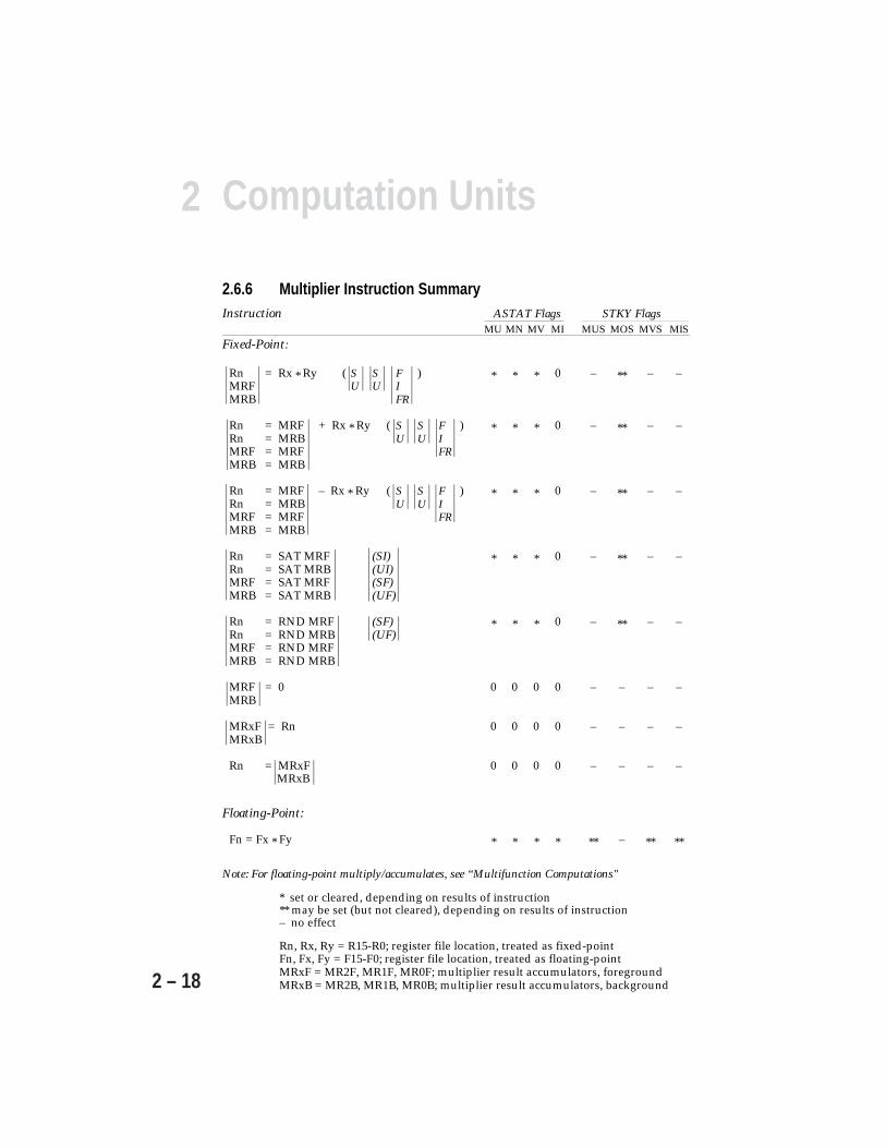
2 Computation Units
2 – 18
2.6.6 Multiplier Instruction SummaryInstruction ASTAT Flags STKY Flags
MU MN MV MI MUS MOS MVS MISFixed-Point:
Rn = Rx * Ry ( S S F ) * * * 0 – ** – –MRF U U IMRB FR
Rn = MRF + Rx * Ry ( S S F ) * * * 0 – ** – –Rn = MRB U U IMRF = MRF FRMRB = MRB
Rn = MRF – Rx * Ry ( S S F ) * * * 0 – ** – –Rn = MRB U U IMRF = MRF FRMRB = MRB
Rn = SAT MRF (SI) * * * 0 – ** – –Rn = SAT MRB (UI)MRF = SAT MRF (SF)MRB = SAT MRB (UF)
Rn = RND MRF (SF) * * * 0 – ** – –Rn = RND MRB (UF)MRF = RND MRFMRB = RND MRB
MRF = 0 0 0 0 0 – – – –MRB
MRxF = Rn 0 0 0 0 – – – –MRxB
Rn = MRxF 0 0 0 0 – – – – MRxB
Floating-Point:
Fn = Fx * Fy * * * * ** – ** **
Note: For floating-point multiply/accumulates, see “Multifunction Computations"
* set or cleared, depending on results of instruction** may be set (but not cleared), depending on results of instruction– no effect
Rn, Rx, Ry = R15-R0; register file location, treated as fixed-pointFn, Fx, Fy = F15-F0; register file location, treated as floating-pointMRxF = MR2F, MR1F, MR0F; multiplier result accumulators, foregroundMRxB = MR2B, MR1B, MR0B; multiplier result accumulators, background
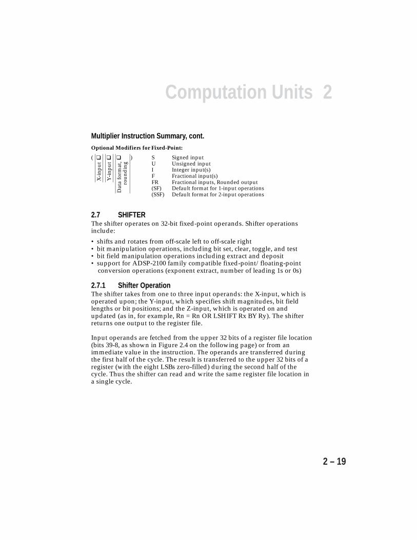
2Computation Units
2 – 19
Multiplier Instruction Summary, cont.Optional Modifiers for Fixed-Point:
( ) S Signed inputU Unsigned inputI Integer input(s)F Fractional input(s)FR Fractional inputs, Rounded output(SF) Default format for 1-input operations(SSF) Default format for 2-input operations
2.7 SHIFTERThe shifter operates on 32-bit fixed-point operands. Shifter operationsinclude:
• shifts and rotates from off-scale left to off-scale right• bit manipulation operations, including bit set, clear, toggle, and test• bit field manipulation operations including extract and deposit• support for ADSP-2100 family compatible fixed-point/floating-point
conversion operations (exponent extract, number of leading 1s or 0s)
2.7.1 Shifter OperationThe shifter takes from one to three input operands: the X-input, which isoperated upon; the Y-input, which specifies shift magnitudes, bit fieldlengths or bit positions; and the Z-input, which is operated on andupdated (as in, for example, Rn = Rn OR LSHIFT Rx BY Ry). The shifterreturns one output to the register file.
Input operands are fetched from the upper 32 bits of a register file location(bits 39-8, as shown in Figure 2.4 on the following page) or from animmediate value in the instruction. The operands are transferred duringthe first half of the cycle. The result is transferred to the upper 32 bits of aregister (with the eight LSBs zero-filled) during the second half of thecycle. Thus the shifter can read and write the same register file location ina single cycle.
X-i
nput
Y-i
nput
Dat
a fo
rmat
,ro
und
ing

2 Computation Units
2 – 20
The X-input and Z-input are always 32-bit fixed-point values. The Y-inputis a 32-bit fixed-point value or an 8-bit field (shf8), positioned in theregister file as shown in Figure 2.4 below.
Some shifter operations produce 8-bit or 6-bit results. These results areplaced in either the shf8 field or the bit6 field (see Figure 2.5) and are sign-extended to 32 bits. Thus the shifter always returns a 32-bit result.
shf8
715 039
039 7
32-Bit Y-Input or Result
8-Bit Y-Input or Result
Figure 2.4 Register File Fields For Shifter Instructions
2.7.2 Bit Field Deposit & Extract InstructionsThe shifter’s bit field deposit and bit field extract instructions allow themanipulation of groups of bits within a 32-bit fixed-point integer word.
The Y-input for these instructions specifies two 6-bit values, bit6 and len6,positioned in the Ry register as shown in Figure 2.5. Bit6 and len6 areinterpreted as positive integers. Bit6 is the starting bit position for thedeposit or extract. Len6 is the bit field length, which specifies how manybits are deposited or extracted.
039
len6
719
bit6
13
12-Bit Y-Input
Figure 2.5 Register File Fields For FDEP, FEXT Instructions
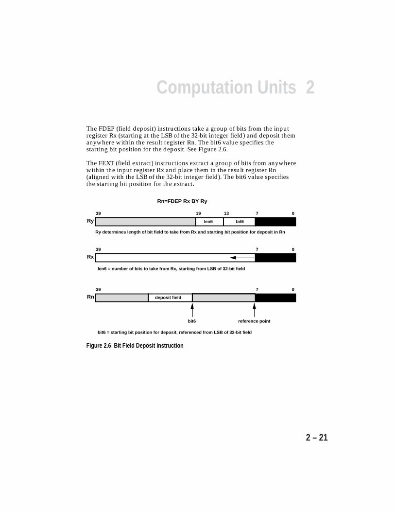
2Computation Units
2 – 21
The FDEP (field deposit) instructions take a group of bits from the inputregister Rx (starting at the LSB of the 32-bit integer field) and deposit themanywhere within the result register Rn. The bit6 value specifies thestarting bit position for the deposit. See Figure 2.6.
The FEXT (field extract) instructions extract a group of bits from anywherewithin the input register Rx and place them in the result register Rn(aligned with the LSB of the 32-bit integer field). The bit6 value specifiesthe starting bit position for the extract.
039
len6
719
bit6
13
Ry determines length of bit field to take from Rx and starting bit position for deposit in Rn
Ry
039 7
Rx
len6 = number of bits to take from Rx, starting from LSB of 32-bit field
039 7
Rn
bit6 = starting bit position for deposit, referenced from LSB of 32-bit field
Rn=FDEP Rx BY Ry
deposit field
bit6 reference point
Figure 2.6 Bit Field Deposit Instruction

2 Computation Units
2 – 22
The following field deposit instruction example is pictured in Figure 2.7:
R0=FDEP R1 BY R2;
R2
R0=FDEP R1 BY R2;
0x0000 0210 0000000000 00000000 00000010 00010000 00000000
bit6len6len6 = 8bit6 = 16
39 08162432
8 bits are taken from R1 and deposited in R0, starting at bit 16.("Bit 16" is relative to reference point, the LSB of 32-bit integer field.)
R0 0x00FF 0000 00
39 08162432
00000000 11111111 00000000 00000000 00000000
reference point
starting bitposition fordeposit
081624
R1=0x000000FF00R2=0x0000021000
R1 0x0000 00FF 0000000000 00000000 00000000 11111111 00000000
39 08162432
Figure 2.7 Bit Field Deposit Example
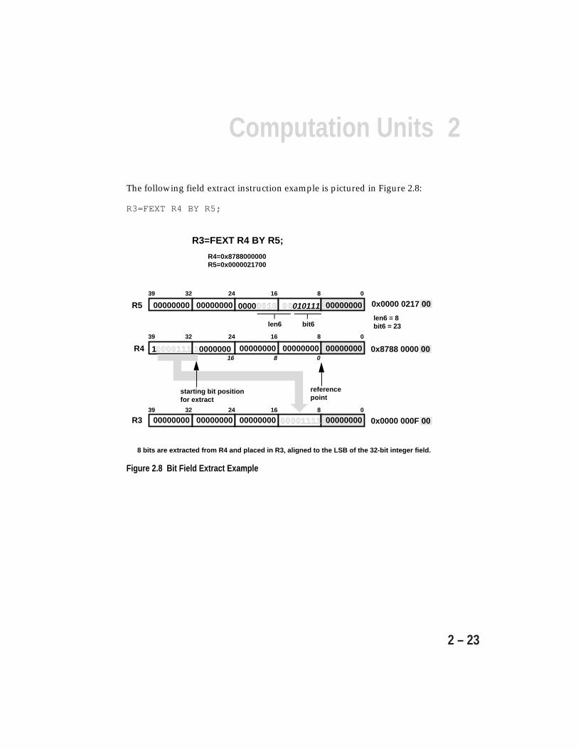
2Computation Units
2 – 23
The following field extract instruction example is pictured in Figure 2.8:
R3=FEXT R4 BY R5;
R5
R4
R3
R3=FEXT R4 BY R5;
0x8788 0000 00
0x0000 000F 00
0x0000 0217 0000000000 00000000 00000010 00010111 00000000
10000111 10000000 00000000 00000000 00000000
39 08162432
00000000 00000000 00000000 00001111 00000000
len6 = 8bit6 = 23
8 bits are extracted from R4 and placed in R3, aligned to the LSB of the 32-bit integer field.
reference point
starting bit positionfor extract
39 08162432
39 08162432
0816
R4=0x8788000000R5=0x0000021700
bit6len6
Figure 2.8 Bit Field Extract Example
2 Computation Units
2 – 24
2.7.3 Shifter Status FlagsThe shifter returns three status flags at the end of the operation. All ofthese flags appear in the ASTAT register. The SZ flag indicates if theoutput is zero, the SV flag indicates an overflow, and the SS flag indicatesthe sign bit in exponent extract operations.
ASTATBit Name Definition11 SV Shifter overflow of bits to left of MSB12 SZ Shifter result zero13 SS Shifter input sign (for exponent extract only)
Flag update occurs at the end of the cycle in which the status is generatedand is available on the next cycle. If a program writes the ASTAT registerexplicitly in the same cycle that the shifter is performing an operation, theexplicit write to ASTAT supersedes any flag update caused by the shiftoperation.
2.7.3.1 Shifter Zero Flag (SZ)SZ is affected by all shifter operations. It is set whenever:
• the result of a shifter operation is zero, or• a bit test instruction specifies a bit outside of the 32-bit fixed-point field.
SZ is otherwise cleared.
2.7.3.2 Shifter Overflow Flag (SV)SV is affected by all shifter operations. It is set whenever:
• significant bits are shifted to the left of the 32-bit fixed-point field,• a bit outside of the 32-bit fixed-point field is tested, set or cleared,• a field that is partially or wholly to the left of the 32-bit fixed-point field
is extracted, or• a LEFTZ or LEFTO operation returns a result of 32.
SV is otherwise cleared.
2.7.3.3 Shifter Sign Flag (SS)SS is affected by all shifter operations. For the two EXP (exponentextract) operations, it is set if the fixed-point input operand is negativeand cleared if it is positive. For all other shifter operations, SS iscleared.
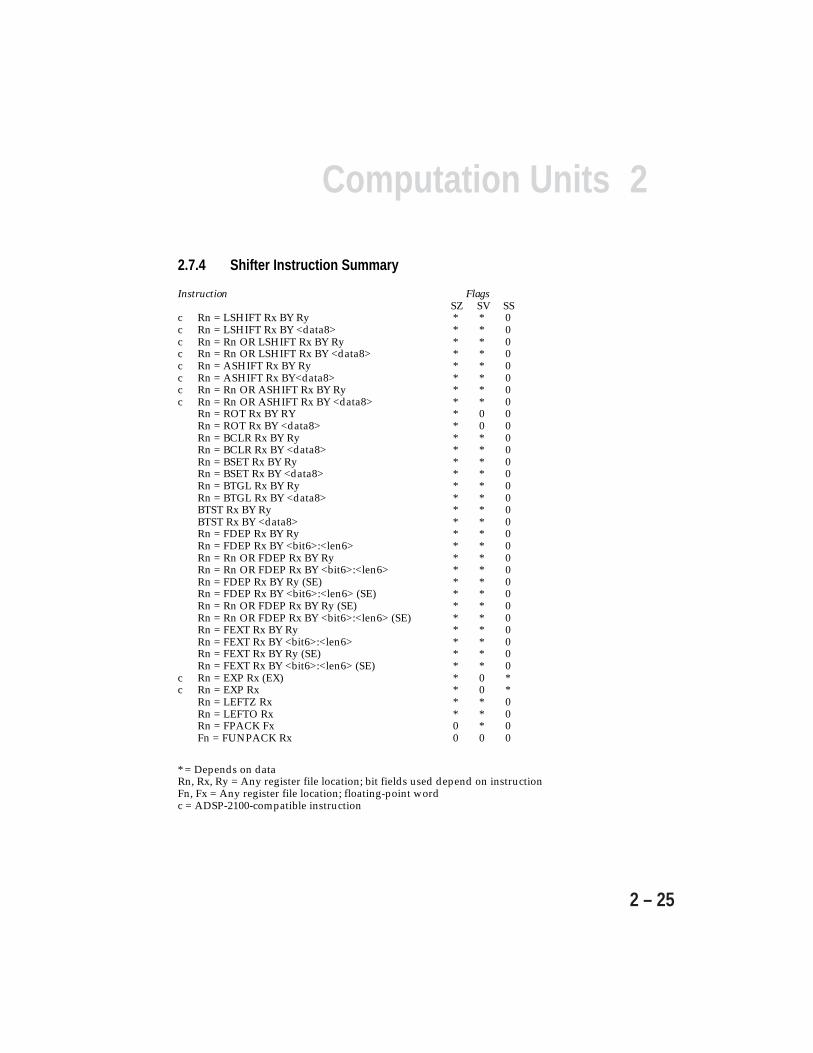
2Computation Units
2 – 25
2.7.4 Shifter Instruction Summary
Instruction FlagsSZ SV SS
c Rn = LSHIFT Rx BY Ry * * 0c Rn = LSHIFT Rx BY <data8> * * 0c Rn = Rn OR LSHIFT Rx BY Ry * * 0c Rn = Rn OR LSHIFT Rx BY <data8> * * 0c Rn = ASHIFT Rx BY Ry * * 0c Rn = ASHIFT Rx BY<data8> * * 0c Rn = Rn OR ASHIFT Rx BY Ry * * 0c Rn = Rn OR ASHIFT Rx BY <data8> * * 0
Rn = ROT Rx BY RY * 0 0Rn = ROT Rx BY <data8> * 0 0Rn = BCLR Rx BY Ry * * 0Rn = BCLR Rx BY <data8> * * 0Rn = BSET Rx BY Ry * * 0Rn = BSET Rx BY <data8> * * 0Rn = BTGL Rx BY Ry * * 0Rn = BTGL Rx BY <data8> * * 0BTST Rx BY Ry * * 0BTST Rx BY <data8> * * 0Rn = FDEP Rx BY Ry * * 0Rn = FDEP Rx BY <bit6>:<len6> * * 0Rn = Rn OR FDEP Rx BY Ry * * 0Rn = Rn OR FDEP Rx BY <bit6>:<len6> * * 0Rn = FDEP Rx BY Ry (SE) * * 0Rn = FDEP Rx BY <bit6>:<len6> (SE) * * 0Rn = Rn OR FDEP Rx BY Ry (SE) * * 0Rn = Rn OR FDEP Rx BY <bit6>:<len6> (SE) * * 0Rn = FEXT Rx BY Ry * * 0Rn = FEXT Rx BY <bit6>:<len6> * * 0Rn = FEXT Rx BY Ry (SE) * * 0Rn = FEXT Rx BY <bit6>:<len6> (SE) * * 0
c Rn = EXP Rx (EX) * 0 *c Rn = EXP Rx * 0 *
Rn = LEFTZ Rx * * 0Rn = LEFTO Rx * * 0Rn = FPACK Fx 0 * 0Fn = FUNPACK Rx 0 0 0
* = Depends on dataRn, Rx, Ry = Any register file location; bit fields used depend on instructionFn, Fx = Any register file location; floating-point wordc = ADSP-2100-compatible instruction
2 Computation Units
2 – 26
2.8 MULTIFUNCTION COMPUTATIONSIn addition to the computations performed by each computation unit, theADSP-2106x also provides multifunction computations that combineparallel operation of the multiplier and the ALU, or dual functions in theALU. The two operations are performed in the same way as they are incorresponding single-function computations. Flags are also determined inthe same way as for the same single-function computations, except that inthe dual add/subtract computation the ALU flags from the twooperations are ORed together.
Each of the four input operands for computations that use both the ALUand multiplier are constrained to a different set of four register filelocations, as summarized below and shown in Figure 2.9. For example, theX-input to the ALU can only be R8, R9, R10 or R11. In all other operations,the input operands may be any register file locations.
Dual Add/Subtract
Ra = Rx + Ry , Rs = Rx – RyFa = Fx + Fy , Fs = Fx – Fy
Fixed-Point Multiply/Accumulate and Add, Subtract or Average
Rm=R3-0 * R7-4 (SSFR) , Ra=R11-8 + R15-12 MRF=MRF + R3-0 * R7-4 (SSF) , Ra=R11-8 – R15-12 Rm=MRF + R3-0 * R7-4 (SSFR) , Ra=(R11-8 + R15-12)/2 MRF=MRF – R3-0 * R7-4 (SSF) , Rm=MRF – R3-0 * R7-4 (SSFR) ,
Floating-Point Multiplication and ALU Operation
Fm=F3-0 * F7-4 , Fa=F11-8 + F15-12Fa=F11-8 – F15-12Fa=FLOAT R11-8 by R15-12Ra=FIX F11-8 by R15-12Fa=(F11-8 + F15-12)/2Fa=ABS F11-8Fa=MAX (F11-8, F15-12)Fa=MIN (F11-8, F15-12)
Multiplication and Dual Add/Subtract
Rm = R3-0 * R7-4 (SSFR) , Ra = R11-8 + R15-12 , Rs = R11-8 – R15-12Fm = F3-0 * F7-4 , Fa = F11-8 + F15-12 , Fs = F11-8 – F15-12
Rm, Ra, Rs, Rx, Ry –Any register file location; fixed-pointFm, Fa, Fs, Fx, Fy –Any register file location; floating-point
R3-0 –R3, R2, R1, R0 F3-0 –F3, F2, F1, F0R7-4 –R7, R6, R5, R4 F7-4 –F7, F6, F5, F4R11-8 –R11, R10, R9, R8 F11-8 –F11, F10, F9, F8R15-12 –R15, R14, R13, R12 F15-12 –F15, F14, F13, F12
SSFR –X-input signed, Y-input signed, Fractional input, Rounded-to-nearest outputSSF –X-input signed, Y-input signed, Fractional input
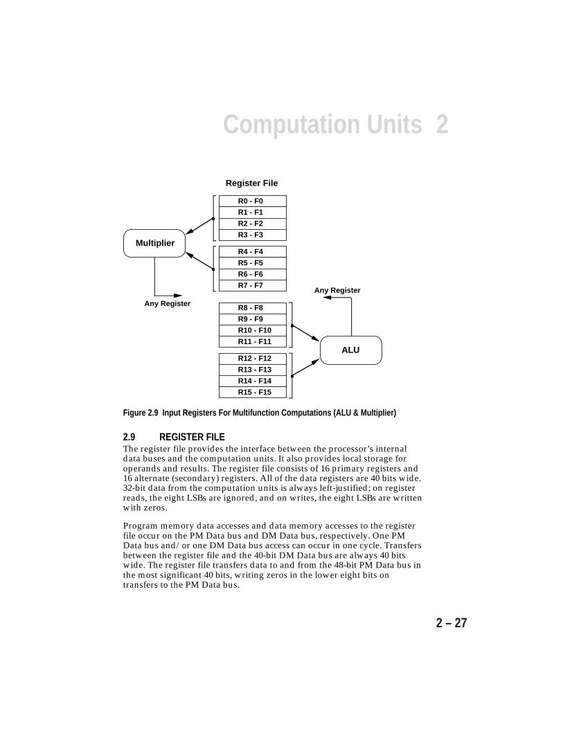
2Computation Units
2 – 27
R0 - F0
R1 - F1
R2 - F2
R3 - F3
R4 - F4
R5 - F5
R6 - F6
R7 - F7
R8 - F8
R9 - F9
R10 - F10
R11 - F11
R12 - F12
R13 - F13
R14 - F14
R15 - F15
Multiplier
ALU
Any Register
Any Register
Register File
Figure 2.9 Input Registers For Multifunction Computations (ALU & Multiplier)
2.9 REGISTER FILEThe register file provides the interface between the processor’s internaldata buses and the computation units. It also provides local storage foroperands and results. The register file consists of 16 primary registers and16 alternate (secondary) registers. All of the data registers are 40 bits wide.32-bit data from the computation units is always left-justified; on registerreads, the eight LSBs are ignored, and on writes, the eight LSBs are writtenwith zeros.
Program memory data accesses and data memory accesses to the registerfile occur on the PM Data bus and DM Data bus, respectively. One PMData bus and/or one DM Data bus access can occur in one cycle. Transfersbetween the register file and the 40-bit DM Data bus are always 40 bitswide. The register file transfers data to and from the 48-bit PM Data bus inthe most significant 40 bits, writing zeros in the lower eight bits ontransfers to the PM Data bus.
2 Computation Units
2 – 28
If the same register file location is specified as both the source of anoperand and the destination of a result or memory fetch, the read occursin the first half of the cycle and the write in the second half. Thus the olddata is used as the operand before the location is updated with the newresult data. If writes to the same location take place in the same cycle, onlythe write with higher precedence actually occurs. Precedence isdetermined by the source of the data being written; from highest tolowest, the precedence is:
• Data memory or universal register• Program memory• ALU• Multiplier• Shifter
The individual registers of the register file are prefixed with an “F” whenused in floating-point computations (in assembly language source code).The registers are prefixed with an “R” when used in fixed-pointcomputations. The following instructions, for example, use the sameregisters:
F0=F1 * F2; floating-point multiplyR0=R1 * R2; fixed-point multiply
The F and R prefixes do not affect the 32-bit (or 40-bit) data transfer; theyonly determine how the ALU, multiplier, or shifter treat the data. The F orR may be either uppercase or lowercase; the assembler is case-insensitive.
2.9.1 Alternate (Secondary) RegistersTo facilitate fast context switching, the register file has an alternate registerset. Each half of the register file—the lower half, R0 through R7, and theupper half, R8 through R15—can independently activate its alternateregister set. Two bits in the MODE1 register select the active sets. Data canbe shared between contexts by placing the data to be shared in one half ofthe register file and activating the alternate register set of the other half.

2Computation Units
2 – 29
MODE1Bit Name Definition7 SRRFH Register file alternate select for R15-R8 (F15-F8)10 SRRFL Register file alternate select for R7-R0 (F7-F0)
Note that there is one cycle of effect latency from the instruction settingthe bit in MODE1 to when the alternate registers may be accessed. Forexample,
BIT SET MODE1 SRRFL; /* activate alternate registers */NOP; /* wait until alternate registers activate */R0=7;

2 Computation Units
2 – 30
3Program Sequencing
3 – 1
3.1 OVERVIEWProgram flow in the ADSP-2106x is most often linear; the processorexecutes program instructions sequentially. Variations in this linear floware provided by the following program structures, illustrated inFigure 3.1 on the following page:
• Loops. One sequence of instructions is executed several times with zerooverhead.
• Subroutines. The processor temporarily interrupts sequential flow toexecute instructions from another part of program memory.
• Jumps. Program flow is permanently transferred to another part ofprogram memory.
• Interrupts. A special case of subroutines in which the execution of theroutine is triggered by an event that happens at run time, not by aprogram instruction.
• Idle. A special instruction that causes the processor to cease operations,holding its current state. When an interrupt occurs, the processorservices the interrupt and continues normal execution.
Managing these program structures is the job of the ADSP-2106x’sprogram sequencer. The program sequencer selects the address of the nextinstruction, generating most of those addresses itself. It also performs awide range of related functions, such as
• incrementing the fetch address,• maintaining stacks,• evaluating conditions,• decrementing the loop counter,• calculating new addresses,• maintaining an instruction cache, and• handling interrupts.
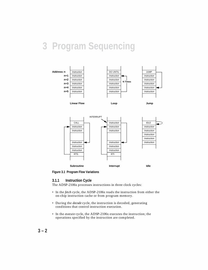
3 Program Sequencing
3 – 2
DO UNTIL
Instruction
Instruction
Instruction
Instruction
Instruction
JUMP
Instruction
Instruction
Instruction
Instruction
Instruction
N Times
nn+1
n+2
n+3
n+4
n+5
Address:
CALL
Instruction
Instruction
Instruction
Instruction
Instruction
RTS
INTERRUPT
Instruction
Instruction
Instruction
Instruction
Instruction
RTI
Instruction IDLE
Instruction
Instruction
Instruction
Instruction
Instruction
Instruction
Instruction
Instruction
Instruction
Instruction
Instruction
Linear Flow Loop Jump
Subroutine Interrupt Idle
Figure 3.1 Program Flow Variations
3.1.1 Instruction CycleThe ADSP-2106x processes instructions in three clock cycles:
• In the fetch cycle, the ADSP-2106x reads the instruction from either theon-chip instruction cache or from program memory.
• During the decode cycle, the instruction is decoded, generatingconditions that control instruction execution.
• In the execute cycle, the ADSP-2106x executes the instruction; theoperations specified by the instruction are completed.

3Program Sequencing
3 – 3
These cycles are overlapping, or pipelined, as shown in Figure 3.2. Insequential program flow, when one instruction is being fetched, theinstruction fetched in the previous cycle is being decoded, and theinstruction fetched two cycles before is being executed. Thus, thethroughput is one instruction per cycle.
Fetch Execute
0x08
0x09
0x080x0A
0x090x0B
0x0A0x0C
Decode
0x08
0x09
0x0A
0x0B
time(cycles)
1
2
3
4
5
Figure 3.2 Pipelined Execution Cycles
Any non-sequential program flow can potentially decrease theADSP-2106x’s instruction throughput. Non-sequential programoperations include:
• Program memory data accesses that conflict with instruction fetches• Jumps• Subroutine Calls and Returns• Interrupts and Returns• Loops
3.1.2 Program Sequencer ArchitectureFigure 3.3, on the next page, shows a block diagram of the programsequencer. The sequencer selects the value of the next fetch address fromseveral possible sources.
The fetch address register, decode address register and program counter(PC) contain, respectively, the addresses of the instructions currentlybeing fetched, decoded and executed. The PC is coupled with the PCstack, which is used to store return addresses and top-of-loop addresses.

3 Program Sequencing
3 – 4
CONDITION LOGIC
LOOP CONTROLLER
LOOP COUNT STACK
FETCH ADDRESS
DECODE ADDRESS
PROGRAM COUNTER
PC STACK
ASTAT MODE1
STATUS STACK
INTERRUPT CONTROLLER
INTERRUPT LATCH
INTERRUPT MASK
INTERRUPT MASK POINTER
INSTRUCTION CACHE
INPUT FLAGS
NEXT ADDRESS MULTIPLEXER
INTERRUPTS
PMA BUS
DAG2
INDIRECTBRANCH
RETURN ADDRESS ORTOP OF LOOP
INTERRUPTVECTOR
+1
INTERNAL PMD BUS
+
DIRECTBRANCH
PC-RELATIVEADDRESS
LOOP ADDRESSSTACK
INTERRUPTLOGIC
LOOP LOGIC
INSTRUCTION LATCH
Figure 3.3 Program Sequencer Block Diagram
The interrupt controller performs all functions related to interruptprocessing, such as determining whether an interrupt is masked andgenerating the appropriate interrupt vector address.
The instruction cache provides the means by which the ADSP-2106x canaccess data in program memory and fetch an instruction (from the cache)in the same cycle. The DAG2 data address generator (described in the nextchapter) outputs program memory data addresses.
The sequencer evaluates conditional instructions and loop terminationconditions using information from the status registers. The loop addressstack and loop counter stack support nested loops. The status stack storesstatus registers for implementing nested interrupt routines.
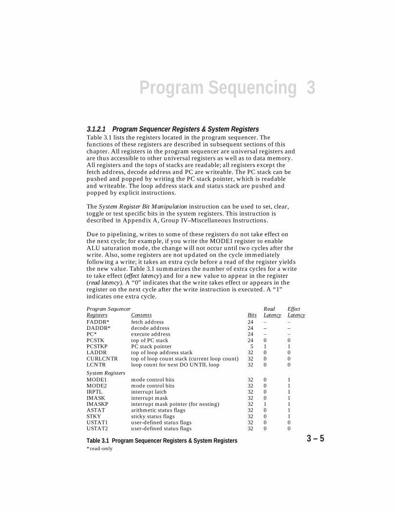
3Program Sequencing
3 – 5
3.1.2.1 Program Sequencer Registers & System RegistersTable 3.1 lists the registers located in the program sequencer. Thefunctions of these registers are described in subsequent sections of thischapter. All registers in the program sequencer are universal registers andare thus accessible to other universal registers as well as to data memory.All registers and the tops of stacks are readable; all registers except thefetch address, decode address and PC are writeable. The PC stack can bepushed and popped by writing the PC stack pointer, which is readableand writeable. The loop address stack and status stack are pushed andpopped by explicit instructions.
The System Register Bit Manipulation instruction can be used to set, clear,toggle or test specific bits in the system registers. This instruction isdescribed in Appendix A, Group IV–Miscellaneous Instructions.
Due to pipelining, writes to some of these registers do not take effect onthe next cycle; for example, if you write the MODE1 register to enableALU saturation mode, the change will not occur until two cycles after thewrite. Also, some registers are not updated on the cycle immediatelyfollowing a write; it takes an extra cycle before a read of the register yieldsthe new value. Table 3.1 summarizes the number of extra cycles for a writeto take effect (effect latency) and for a new value to appear in the register(read latency). A “0” indicates that the write takes effect or appears in theregister on the next cycle after the write instruction is executed. A “1”indicates one extra cycle.
Program Sequencer Read EffectRegisters Contents Bits Latency LatencyFADDR* fetch address 24 – –DADDR* decode address 24 – –PC* execute address 24 – –PCSTK top of PC stack 24 0 0PCSTKP PC stack pointer 5 1 1LADDR top of loop address stack 32 0 0CURLCNTR top of loop count stack (current loop count) 32 0 0LCNTR loop count for next DO UNTIL loop 32 0 0System RegistersMODE1 mode control bits 32 0 1MODE2 mode control bits 32 0 1IRPTL interrupt latch 32 0 1IMASK interrupt mask 32 0 1IMASKP interrupt mask pointer (for nesting) 32 1 1ASTAT arithmetic status flags 32 0 1STKY sticky status flags 32 0 1USTAT1 user-defined status flags 32 0 0USTAT2 user-defined status flags 32 0 0
Table 3.1 Program Sequencer Registers & System Registers* read-only

3 Program Sequencing
3 – 6
3.2 PROGRAM SEQUENCER OPERATIONSThis section gives an overview of the operation of the program sequencer.The various kinds of program flow are defined here and described indetail in subsequent sections.
3.2.1 Sequential Instruction FlowThe program sequencer determines the next instruction address byexamining both the current instruction being executed and the currentstate of the processor. If no conditions require otherwise, the ADSP-2106xexecutes instructions from program memory in sequential order by simplyincrementing the fetch address.
3.2.2 Program Memory Data AccessesUsually, the ADSP-2106x fetches an instruction from memory on eachcycle. When the ADSP-2106x executes an instruction which requires datato be read from or written to the same memory block in which theinstruction is stored, there is a conflict for access to that block. TheADSP-2106x uses its instruction cache to reduce delays caused by this typeof conflict.
The first time the ADSP-2106x encounters an instruction fetch thatconflicts with a program memory data access, it must wait to fetch theinstruction on the following cycle, causing a delay. The ADSP-2106xautomatically writes the fetched instruction to the cache to prevent thesame delay from happening again. The ADSP-2106x checks the instructioncache on every program memory data access. If the instruction needed isin the cache, the instruction fetch from the cache happens in parallel withthe program memory data access, without incurring a delay.
3.2.3 BranchesA branch occurs when the fetch address is not the next sequential addressfollowing the previous fetch address. Jumps, calls and returns are thetypes of branches which the ADSP-2106x supports. In the programsequencer, the only difference between a jump and a call is that uponexecution of a call, a return address is pushed onto the PC stack so that itis available when a return instruction is later executed. Jumps branch to anew location without allowing return.
3.2.4 LoopsThe ADSP-2106x supports program loops with the DO UNTIL instruction.The DO UNTIL instruction causes the ADSP-2106x to repeat a sequence ofinstructions until a specified condition tests true.
3Program Sequencing
3 – 7
3.3 CONDITIONAL INSTRUCTION EXECUTIONThe program sequencer evaluates conditions to determine whether toexecute a conditional instruction and when to terminate a loop. Theconditions are based on information from the arithmetic status (ASTAT)register, mode control 1 (MODE1) register, flag inputs and loop counter.The arithmetic ASTAT bits are described in the previous chapter,Computation Units.
Each condition that the ADSP-2106x evaluates has an assemblermnemonic and a unique code which is used in a conditional instruction’sopcode. For most conditions, the program sequencer can test both trueand false states, e.g., equal to zero and not equal to zero. Table 3.2, on thefollowing page, defines the 32 condition and termination codes.
The bit test flag (BTF) is bit 18 of the ASTAT register. This flag is set (orcleared) by the results of the BIT TST and BIT XOR forms of theSystem Register Bit Manipulation instruction, which can be used to test thecontents of the ADSP-2106x’s system registers. This instruction isdescribed in Appendix A, Group IV–Miscellaneous instructions. After BTFis set by this instruction, it can be used as the condition in a conditionalinstruction (with the mnemonic TF; see Table 3.2).
The two conditions that do not have complements are LCE/NOT LCE(loop counter expired/not expired) and TRUE/FOREVER. Theinterpretation of these condition codes is determined by context; TRUEand NOT LCE are used in conditional instructions, FOREVER and LCE inloop termination. The IF TRUE construct creates an unconditionalinstruction (the same effect as leaving out the condition entirely). A DOFOREVER instruction executes a loop indefinitely, until an interrupt orreset intervenes.
The LCE condition (loop counter expired) is most commonly used in aDO UNTIL instruction. Because the LCE condition checks the value of theloop counter (CURLCNTR), an IF NOT LCE conditional instructionshould not follow a write to CURLCNTR from memory. Otherwise,because the write occurs after the NOT LCE test, the condition is based onthe old CURLCNTR value.
The bus master condition (BM) indicates whether the ADSP-2106x is thecurrent bus master in a multiprocessor system. To enable the use of thiscondition, bits 17 and 18 of the MODE1 register must both be zeros;otherwise the condition is always evaluated as false.
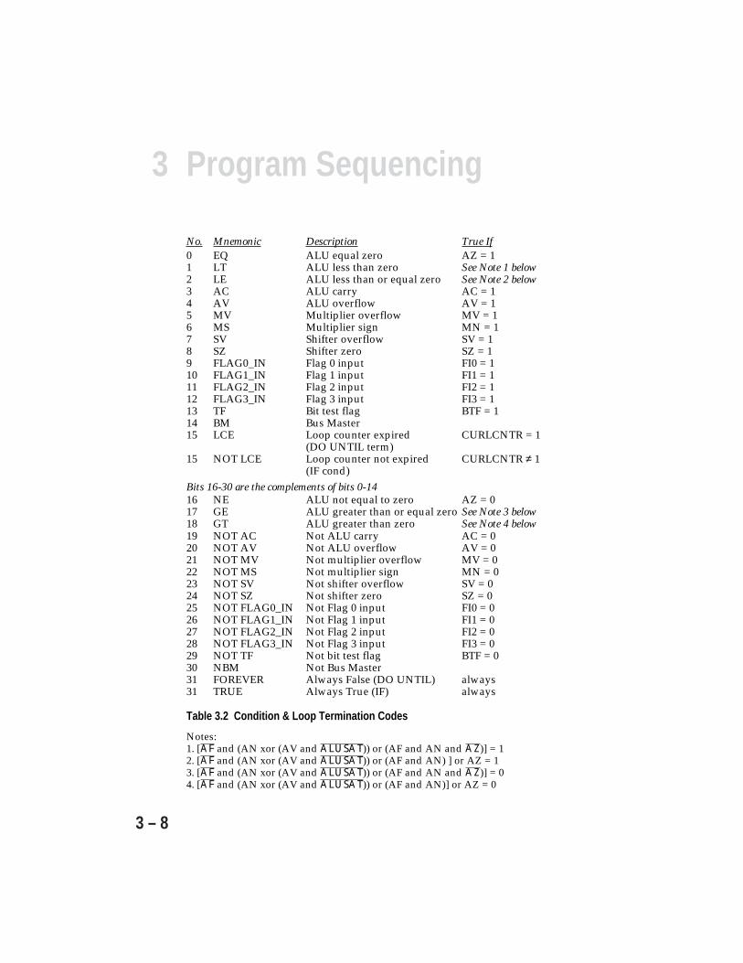
3 Program Sequencing
3 – 8
No. Mnemonic Description True If0 EQ ALU equal zero AZ = 11 LT ALU less than zero See Note 1 below2 LE ALU less than or equal zero See Note 2 below3 AC ALU carry AC = 14 AV ALU overflow AV = 15 MV Multiplier overflow MV = 16 MS Multiplier sign MN = 17 SV Shifter overflow SV = 18 SZ Shifter zero SZ = 19 FLAG0_IN Flag 0 input FI0 = 110 FLAG1_IN Flag 1 input FI1 = 111 FLAG2_IN Flag 2 input FI2 = 112 FLAG3_IN Flag 3 input FI3 = 113 TF Bit test flag BTF = 114 BM Bus Master15 LCE Loop counter expired CURLCNTR = 1
(DO UNTIL term)15 NOT LCE Loop counter not expired CURLCNTR ≠ 1
(IF cond)Bits 16-30 are the complements of bits 0-1416 NE ALU not equal to zero AZ = 017 GE ALU greater than or equal zero See Note 3 below18 GT ALU greater than zero See Note 4 below19 NOT AC Not ALU carry AC = 020 NOT AV Not ALU overflow AV = 021 NOT MV Not multiplier overflow MV = 022 NOT MS Not multiplier sign MN = 023 NOT SV Not shifter overflow SV = 024 NOT SZ Not shifter zero SZ = 025 NOT FLAG0_IN Not Flag 0 input FI0 = 026 NOT FLAG1_IN Not Flag 1 input FI1 = 027 NOT FLAG2_IN Not Flag 2 input FI2 = 028 NOT FLAG3_IN Not Flag 3 input FI3 = 029 NOT TF Not bit test flag BTF = 030 NBM Not Bus Master31 FOREVER Always False (DO UNTIL) always31 TRUE Always True (IF) always
Table 3.2 Condition & Loop Termination Codes
Notes:1. [AF and (AN xor (AV and ALUSAT)) or (AF and AN and AZ)] = 12. [AF and (AN xor (AV and ALUSAT)) or (AF and AN) ] or AZ = 13. [AF and (AN xor (AV and ALUSAT)) or (AF and AN and AZ)] = 04. [AF and (AN xor (AV and ALUSAT)) or (AF and AN)] or AZ = 0
3Program Sequencing
3 – 9
3.4 BRANCHES (CALL, JUMP, RTS, RTI)The CALL instruction initiates a subroutine. Both jumps and calls transferprogram flow to another memory location, but a call also pushes a returnaddress onto the PC stack so that it is available when a return fromsubroutine instruction is later executed. Jumps branch to a new locationwithout allowing return.
A return causes the processor to branch to the address stored at the top ofthe PC stack. There are two types of returns: return from subroutine (RTS)and return from interrupt (RTI). The difference between the two is that theRTI instruction not only pops the return address off the PC stack, but also:1) pops the status stack if the ASTAT and MODE1 status registers havebeen pushed (if the interrupt was IRQ2-0, the timer interrupt, or the VIRPTvector interrupt), and 2) clears the appropriate bit in the interrupt latchregister (IRPTL) and the interrupt mask pointer (IMASKP).
There are a number of parameters you can specify for branches:
• Jumps, calls and returns can be conditional. The program sequencer canevaluate any one of several status conditions to decide whether thebranch should be taken. If no condition is specified, the branch isalways taken.
• Jumps and calls can be indirect, direct, or PC-relative. An indirect branchgoes to an address supplied by one of the data address generators,DAG2. Direct branches jump to the 24-bit address specified in animmediate field in the branch instruction. PC-relative branches also use avalue specified in the instruction, but the sequencer adds this value tothe current PC value to compute the destination address.
• Jumps, calls and returns can be delayed or nondelayed. In a delayedbranch, the two instructions immediately after the branch instructionare executed; in a nondelayed branch, the program sequencer suppressesthe execution of those two instructions (NOPs are performed instead).
• The JUMP (LA) instruction causes an automatic loop abort if it occursinside a loop. When the loop is aborted, the PC and loop address stacksare popped once, so that if the loop was nested, the stacks still containthe correct values for the outer loop. JUMP (LA) is similar to the breakinstruction of the C programming language used to prematurelyterminate execution of a loop. (Note: JUMP (LA) may not be used in thelast three instructions of a loop.)

3 Program Sequencing
3 – 10
3.4.1 Delayed & Nondelayed BranchesAn instruction modifier (DB) indicates that a branch is delayed; otherwise,it is nondelayed. If the branch is nondelayed, the two instructions after thebranch, which are in the fetch and decode stages, are not executed (seeFigure 3.4); for a call, the decode address (the address of the instructionafter the call) is the return address. During the two no-operation cycles,the first instruction at the branch address is fetched and decoded.
Figure 3.4 Nondelayed Branches
n
n+1->nop
n+2
nop
n+2->nop
r
nop
r
r+1
r
r+1
r+2
n
n+1->nop
n+2
j
j+1
j+2FetchInstruction
DecodeInstruction
ExecuteInstruction nop
n+2->nop
j
nop
j
j+1
NON-DELAYED JUMP OR CALL
NON-DELAYED RETURN
n+2 suppressed; r popped from PC stack
n+1 suppressed
n+2 suppressed; for call, n+1 pushed on PC stack
n = Branch instruction
j = Instruction at Jump or Call address
CLOCK CYCLES
n+1 suppressed
CLOCK CYCLES
FetchInstruction
DecodeInstruction
ExecuteInstruction
r = Instruction at Return address

3Program Sequencing
3 – 11
In a delayed branch, the processor continues to execute two moreinstructions while the instruction at the branch address is fetched anddecoded (see Figure 3.5); in the case of a call, the return address is thethird address after the branch instruction. A delayed branch is moreefficient, but it makes the code harder to understand because of theinstructions between the branch instruction and the actual branch.
n
n+1
n+2
j
j+1
j+2
n+2
j
n+2
j
j+1
for call, n+3 pushed on PC stack
n+1
DELAYED JUMP OR CALL
n
n+1
n+2
r
r+1
r+2
n+2
r
n+2
r
r+1
r popped from PC stack
n+1
DELAYED RETURN
FetchInstruction
DecodeInstruction
ExecuteInstruction
CLOCK CYCLES
FetchInstruction
DecodeInstruction
ExecuteInstruction
CLOCK CYCLES
n = Branch instruction
j = Instruction at Jump or Call address
r = Instruction at Return address
Figure 3.5 Delayed Branches

3 Program Sequencing
3 – 12
Because of the instruction pipeline, a delayed branch instruction and thetwo instructions that follow it must be executed sequentially. Instructionsin the two locations immediately following a delayed branch instructionmay not be any of the following:
• Other Jumps, Calls or Returns• Pushes or Pops of the PC stack• Writes to the PC stack or PC stack pointer• DO UNTIL instruction• IDLE or IDLE16 instruction
These exceptions are checked by the ADSP-21000 Family assembler.
The ADSP-2106x does not process an interrupt in between a delayedbranch instruction and either of the two instructions that follow, sincethese three instructions must be executed sequentially. Any interrupt thatoccurs during these instructions is latched but not processed until thebranch is complete.
A read of the PC stack or PC stack pointer immediately after a delayed callor return is permitted, but it will show that the return address on the PCstack has already been pushed or popped, even though the branch has notoccurred yet.
3.4.2 PC StackThe PC stack holds return addresses for subroutines and interrupt serviceroutines and top-of-loop addresses for loops. The PC stack is 30 locationsdeep by 24 bits wide.
The PC stack is popped during returns from interrupts (RTI), returns fromsubroutines (RTS) and terminations of loops. The stack is full when allentries are occupied, empty when no entries are occupied, and overflowedif a call occurs when the stack is already full. The full and empty flags arestored in the sticky status register (STKY). The full flag causes a maskableinterrupt.
A PC stack interrupt occurs when 29 locations of the PC stack are filled(the almost full state). Entering the interrupt service routine thenimmediately causes a push on the PC stack, making it full. Thus theinterrupt is a stack full interrupt, even though the condition that triggers itis the almost full condition. The other stacks in the sequencer, the loopaddress stack, loop counter stack and status stack, are provided withoverflow interrupts that are activated when a push occurs while the stackis in a full state.

3Program Sequencing
3 – 13
The program counter stack pointer (PCSTKP) is a readable and writeableregister that contains the address of the top of the PC stack. The value ofPCSTKP is zero when the PC stack is empty, 1, 2, ..., 30 when the stackcontains data, and 31 when the stack is overflowed. A write to PCSTKPtakes effect after a one-cycle delay. If the PC stack is overflowed, a write toPCSTKP has no effect.
3.5 LOOPS (DO UNTIL)The DO UNTIL instruction provides for efficient software loops, withoutthe overhead of additional instructions to branch, test a condition, ordecrement a counter. Here is a simple example of an ADSP-2106x loop:
LCNTR=30, DO label UNTIL LCE;R0=DM(I0,M0), F2=PM(I8,M8);R1=R0-R15;
label: F4=F2+F3;
When the ADSP-2106x executes a DO UNTIL instruction, the programsequencer pushes the address of the last loop instruction and thetermination condition for exiting the loop (both specified in theinstruction) onto the loop address stack. It also pushes the top-of-loopaddress, which is the address of the instruction following the DO UNTILinstruction, on the PC stack.
Because of the instruction pipeline (fetch, decode and execute cycles), theprocessor tests the termination condition (and, if the loop is counter-based, decrements the counter) before the end of the loop so that the nextfetch either exits the loop or returns to the top based on the test condition.Specifically, the condition is tested when the instruction two locationsbefore the last instruction in the loop (at location e – 2, where e is the end-of-loop address) is executed. If the termination condition is not satisfied,the processor fetches the instruction from the top-of-loop address storedon the top of the PC stack. If the termination condition is true, thesequencer fetches the next instruction after the end of the loop and popsthe loop stack and PC stack. Loop operation is shown in Figure 3.6, on thenext page.
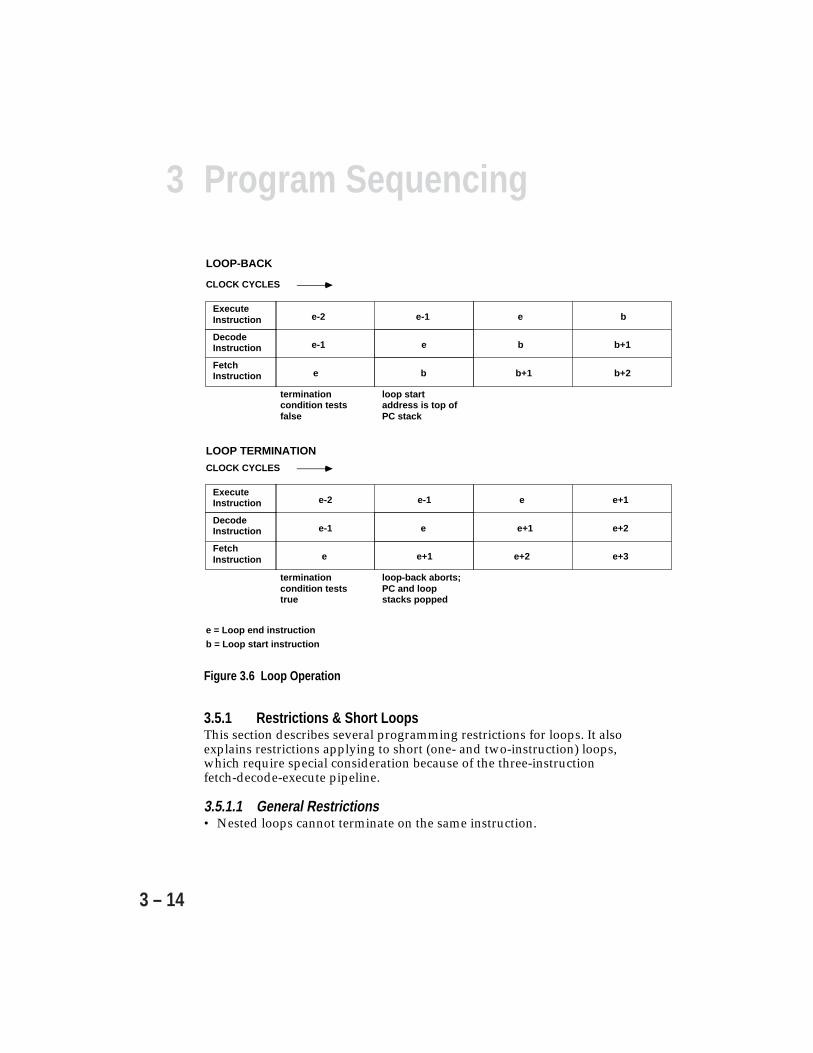
3 Program Sequencing
3 – 14
e-2
e-1
e
e-1
e
b
e
b
b+1
b
b+1
b+2
termination condition tests false
LOOP-BACK
FetchInstruction
DecodeInstruction
ExecuteInstruction
CLOCK CYCLES
e-2
e-1
e
e-1
e
e+1
e
e+1
e+2
e+1
e+2
e+3
loop-back aborts; PC and loop stacks popped
LOOP TERMINATION
termination condition tests true
FetchInstruction
DecodeInstruction
ExecuteInstruction
CLOCK CYCLES
e = Loop end instruction
b = Loop start instruction
loop start address is top of PC stack
Figure 3.6 Loop Operation
3.5.1 Restrictions & Short LoopsThis section describes several programming restrictions for loops. It alsoexplains restrictions applying to short (one- and two-instruction) loops,which require special consideration because of the three-instructionfetch-decode-execute pipeline.
3.5.1.1 General Restrictions• Nested loops cannot terminate on the same instruction.
3Program Sequencing
3 – 15
• The last three instructions of a loop cannot be any branch (jump, call, orreturn); otherwise, the loop may not be executed correctly. This alsoapplies to one-instruction loops and two-instruction loops with onlyone iteration. There is one exception to this rule, a non-delayed CALL(no DB modifier) paired with an RTS (LR), return from subroutine withloop reentry modifier. The non-delayed CALL may be used as one ofthe last three instructions of a loop (but not in a one-instruction loop ora two-instruction, single-iteration loop.)
The RTS (LR) instruction ensures proper reentry into a loop. In counter-based loops, for example, the termination condition is checked bydecrementing the current loop counter (CURLCNTR) during executionof the instruction two locations before the end of the loop. A non-delayed call may then be used in one of the last two locations, providingan RTS (LR) instruction is used to return from the subroutine. The loopreentry (LR) modifier assures proper reentry into the loop, bypreventing the loop counter from being decremented again (i.e. twicefor the same loop iteration).
3.5.1.2 Counter-Based LoopsThe third-to-last instruction of a counter-based loop (at e – 2, where e is theend-of-loop address) cannot be a write to the counter from memory.
Short loops terminate in a special way because of the instruction (fetch-decode-execute) pipeline. Counter-based loops of one or two instructionsare not long enough for the sequencer to check the termination conditiontwo instructions from the end of the loop. In these short loops, thesequencer has already looped back when the termination condition istested. The sequencer provides special handling to avoid overhead (NOP)cycles if the loop is iterated a minimum number of times. The detailedoperation is shown in Figures 3.7 and 3.8 (on the following page). For nooverhead, a loop of length one must be executed at least three times and aloop of length two must be executed at least twice.
Loops of length one that iterate only once or twice and loops of length twothat iterate only once incur two cycles of overhead because there are twoaborted instructions after the last iteration to clear the instruction pipeline.
Processing of an interrupt that occurs during the last iteration of aone-instruction loop that executes once or twice, a two-instruction loopthat executes once, or the cycle following one of these loops (which is aNOP) is delayed by one cycle. Similarly, in a one-instruction loop thatiterates at least three times, processing is delayed by one cycle if theinterrupt occurs during the third-to-last iteration.
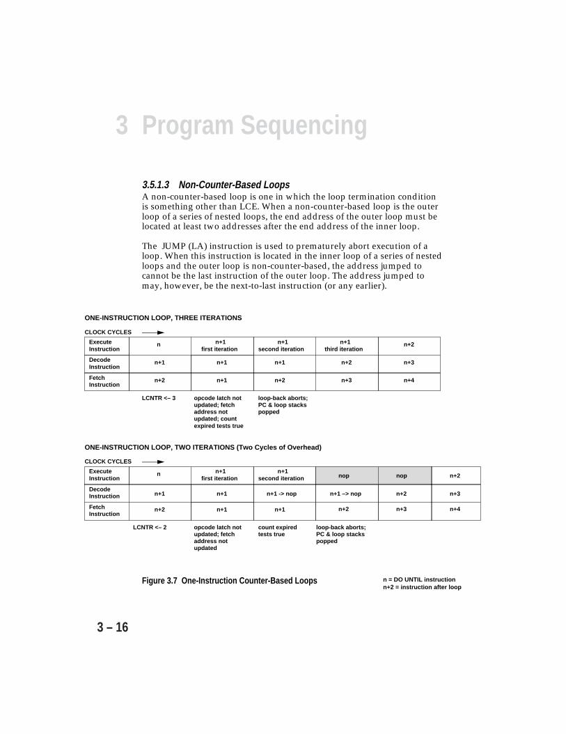
3 Program Sequencing
3 – 16
3.5.1.3 Non-Counter-Based LoopsA non-counter-based loop is one in which the loop termination conditionis something other than LCE. When a non-counter-based loop is the outerloop of a series of nested loops, the end address of the outer loop must belocated at least two addresses after the end address of the inner loop.
The JUMP (LA) instruction is used to prematurely abort execution of aloop. When this instruction is located in the inner loop of a series of nestedloops and the outer loop is non-counter-based, the address jumped tocannot be the last instruction of the outer loop. The address jumped tomay, however, be the next-to-last instruction (or any earlier).
ONE-INSTRUCTION LOOP, THREE ITERATIONS
n
n+1
n+2
opcode latch not updated; fetch address not updated; count expired tests true
LCNTR <– 3
n+1first iteration
n+1
n+1
n+1
n+2
n+2
n+3
n+2
n+3
n+4
loop-back aborts; PC & loop stacks popped
nop
n+2
ONE-INSTRUCTION LOOP, TWO ITERATIONS (Two Cycles of Overhead)
LCNTR <– 2 opcode latch not updated; fetch address not updated
loop-back aborts; PC & loop stacks popped
n+1 –> nop
nop
n+2
n+3
n+2
n+3
n+4
n+1second iteration
n+1third iteration
CLOCK CYCLES
FetchInstruction
DecodeInstruction
ExecuteInstruction
CLOCK CYCLES
FetchInstruction
DecodeInstruction
ExecuteInstruction
n
n+1
n+2
n+1first iteration
n+1
n+1
n+1 -> nop
n+1
n+1second iteration
count expired tests true
Figure 3.7 One-Instruction Counter-Based Loops n = DO UNTIL instructionn+2 = instruction after loop
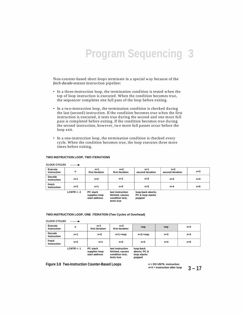
3Program Sequencing
3 – 17
Non-counter-based short loops terminate in a special way because of thefetch-decode-execute instruction pipeline:
• In a three-instruction loop, the termination condition is tested when thetop of loop instruction is executed. When the condition becomes true,the sequencer completes one full pass of the loop before exiting.
• In a two-instruction loop, the termination condition is checked duringthe last (second) instruction. If the condition becomes true when the firstinstruction is executed, it tests true during the second and one more fullpass is completed before exiting. If the condition becomes true duringthe second instruction, however, two more full passes occur before theloop exit.
• In a one-instruction loop, the termination condition is checked everycycle. When the condition becomes true, the loop executes three moretimes before exiting.
TWO-INSTRUCTION LOOP, ONE ITERATION (Two Cycles of Overhead)
n+3
n+4
n+5
n
n+1
n+2
PC stack supplies loop start address
LCNTR <- 1
n+1first iteration
n+2
n+1
n+2first iteration
n+1->nop
n+2
nop
n+2->nop
n+3
nop
n+3
n+4
loop-back aborts; PC & loop stacks popped
last instruction fetched, causes condition test; tests true
TWO-INSTRUCTION LOOP, TWO ITERATIONS
n
n+1
n+2
n+2
n+1
n+1
n+2
n+2
n+3
n+3
n+4
n+3
n+4
n+5
LCNTR <- 2 PC stack supplies loop start address
last instruction fetched, causes condition test; tests true
loop-back aborts; PC & loop stacks popped
CLOCK CYCLES
FetchInstruction
DecodeInstruction
ExecuteInstruction
n+1first iteration
n+2first iteration
n+1second iteration
n+2second iteration
CLOCK CYCLES
FetchInstruction
DecodeInstruction
ExecuteInstruction
n = DO UNTIL instructionn+3 = instruction after loop
Figure 3.8 Two-Instruction Counter-Based Loops

3 Program Sequencing
3 – 18
3.5.2 Loop Address StackThe loop address stack is six levels deep by 32 bits wide. The 32-bit wordof each level consists of a 24-bit loop termination address, a 5-bittermination code, and a 2-bit loop type code:
Bits Value0-23 Loop termination address24-28 Termination code29 reserved (always reads 0)30-31 Loop type code:
00 arithmetic condition-based (not LCE)01 counter-based, length 110 counter-based, length 211 counter-based, length > 2
The loop termination address, termination code and loop type code arestacked when a DO UNTIL or PUSH LOOP instruction is executed. Thestack is popped two instructions before the end of the last loop iteration orwhen a POP LOOP instruction is issued. A stack overflows if a pushoccurs when all entries in the loop stack are occupied. The stack is emptywhen no entries are occupied. The overflow and empty flags are in thesticky status register (STKY). Overflow causes a maskable interrupt.
The LADDR register contains the top of the loop address stack. It isreadable and writeable over the DM Data bus. Reading and writingLADDR does not move the loop address stack pointer; a stack push orpop, performed with explicit instructions, moves the stack pointer.LADDR contains the value 0xFFFF FFFF when the loop address stack isempty.
Because the termination condition is checked two instructions before theend of the loop, the loop stack is popped before the end of the loop on thefinal iteration. If LADDR is read at either of these instructions, the valuewill no longer be the termination address for the loop.
A jump out of a loop pops the loop address stack (and the loop countstack if the loop is counter-based) if the Loop Abort (LA) modifier isspecified for the jump. This allows the loop mechanism to continue tofunction correctly. Only one pop is performed, however, so the loop abortcannot be used to jump more than one level of loop nesting.
3Program Sequencing
3 – 19
3.5.3 Loop Counters And StackThe loop counter stack is six levels deep by 32 bits wide. The loop counterstack works in synchronization with the loop address stack; both stacksalways have the same number of locations occupied. Thus, the sameempty and overflow status flags apply to both stacks.
The ADSP-2106x program sequencer operates two separate loop counters:the current loop counter (CURLCNTR), which tracks iterations for a loopbeing executed, and the loop counter (LCNTR), which holds the countvalue before the loop is executed. Two counters are needed to maintainthe count for an outer loop while setting up the count for an inner loop.
3.5.3.1 CURLCNTRThe top entry in the loop counter stack always contains the loop countcurrently in effect. This entry is the CURLCNTR register, which isreadable and writeable over the DM Data bus. A read of CURLCNTRwhen the loop counter stack is empty gives the value 0xFFFF FFFF.
The program sequencer decrements the value of CURLCNTR for eachloop iteration. Because the termination condition is checked twoinstruction cycles before the end of the loop, the loop counter is alsodecremented before the end of the loop. If CURLCNTR is read at either ofthe last two loop instructions, therefore, the value is already the count forthe next iteration.
The loop counter stack is popped two instructions before the end of thelast loop iteration. When the loop counter stack is popped, the new topentry of the stack becomes the CURLCNTR value, the count in effect forthe executing loop. If there is no executing loop, the value of CURLCNTRis 0xFFFF FFFF after the pop.
Writing CURLCNTR does not cause a stack push. Thus, if you write a newvalue to CURLCNTR, you change the count value of the loop currentlyexecuting. A write to CURLCNTR when no DO UNTIL LCE loop isexecuting has no effect.
Because the processor must use CURLCNTR to perform counter-basedloops, there are some restrictions on when you can write CURLCNTR. Asmentioned under “Loop Restrictions,” the third-to-last instruction of a DOUNTIL LCE loop cannot be a write to CURLCNTR from memory. Theinstruction that follows a write to CURLCNTR from memory cannot be anIF NOT LCE instruction.
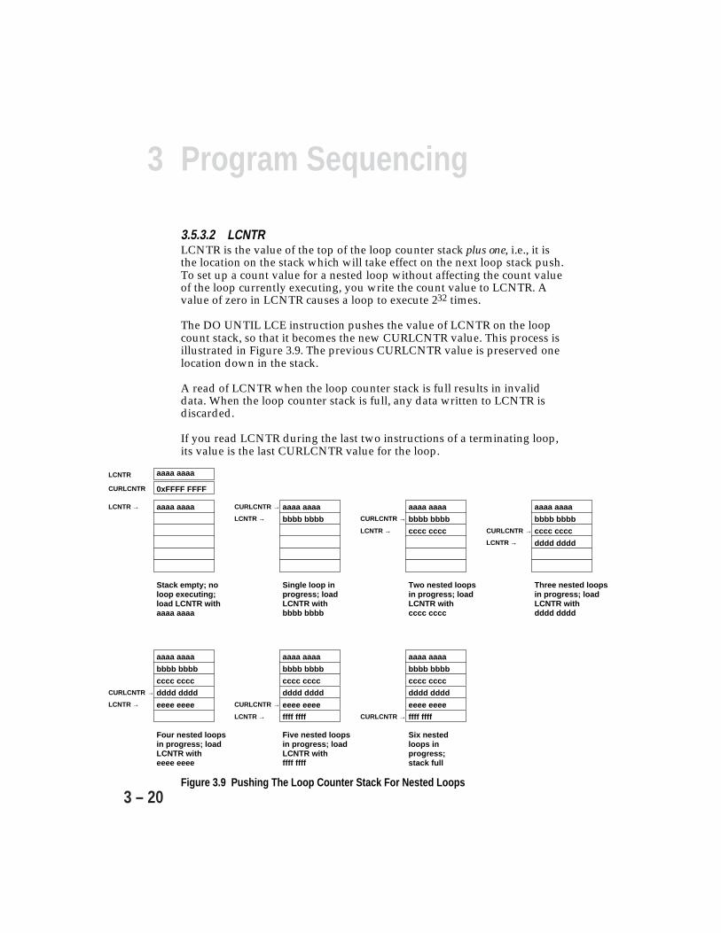
3 Program Sequencing
3 – 20
3.5.3.2 LCNTRLCNTR is the value of the top of the loop counter stack plus one, i.e., it isthe location on the stack which will take effect on the next loop stack push.To set up a count value for a nested loop without affecting the count valueof the loop currently executing, you write the count value to LCNTR. Avalue of zero in LCNTR causes a loop to execute 232 times.
The DO UNTIL LCE instruction pushes the value of LCNTR on the loopcount stack, so that it becomes the new CURLCNTR value. This process isillustrated in Figure 3.9. The previous CURLCNTR value is preserved onelocation down in the stack.
A read of LCNTR when the loop counter stack is full results in invaliddata. When the loop counter stack is full, any data written to LCNTR isdiscarded.
If you read LCNTR during the last two instructions of a terminating loop,its value is the last CURLCNTR value for the loop.
Figure 3.9 Pushing The Loop Counter Stack For Nested Loops
LCNTR →
0xFFFF FFFF
Stack empty; no loop executing; load LCNTR withaaaa aaaa
Six nested loops in progress; stack full
Single loop in progress; load LCNTR withbbbb bbbb
Two nested loops in progress; load LCNTR withcccc cccc
Three nested loops in progress; load LCNTR withdddd dddd
Four nested loops in progress; load LCNTR witheeee eeee
Five nested loops in progress; load LCNTR withffff ffff
aaaa aaaa
CURLCNTR
LCNTR →
CURLCNTR → aaaa aaaa aaaa aaaa
bbbb bbbbLCNTR →
CURLCNTR → bbbb bbbbcccc cccc
aaaa aaaa
LCNTR →
CURLCNTR →
bbbb bbbbcccc cccc
dddd dddd
aaaa aaaa
LCNTR →
CURLCNTR →
bbbb bbbbcccc ccccdddd dddd
eeee eeee
aaaa aaaa
LCNTR →
CURLCNTR →
bbbb bbbbcccc ccccdddd dddd
eeee eeeeffff ffff
aaaa aaaa
CURLCNTR →
bbbb bbbbcccc ccccdddd dddd
eeee eeeeffff ffff
LCNTR aaaa aaaa
3Program Sequencing
3 – 21
3.6 INTERRUPTSInterrupts are caused by a variety of conditions, both internal andexternal to the processor. An interrupt forces a subroutine call to apredefined address, the interrupt vector. The ADSP-2106x assigns aunique vector to each type of interrupt.
Externally, the ADSP-2106x supports three prioritized, individuallymaskable interrupts, each of which can be either level or edge-triggered. These interrupts are caused by an external device assertingone of the ADSP-2106x’s interrupt inputs (IRQ2-0). Among theinternally generated interrupts are arithmetic exceptions, stackoverflows, and circular data buffer overflows.
An interrupt request is deemed valid if it is not masked, if interruptsare globally enabled (if bit 12 in MODE1 is set), and if a higher priorityrequest is not pending. Valid requests invoke an interrupt servicesequence that branches to the address reserved for that interrupt.Interrupt vectors are spaced at 8-instruction intervals; longer serviceroutines can be accommodated by branching to another region ofmemory. Program execution returns to normal sequencing when anRTI (return from interrupt) instruction is executed.
The ADSP-2106x core processor cannot service an interrupt unless it isexecuting instructions or is in the IDLE state. IDLE and IDLE16 are aspecial instructions that halt the processor core until an externalinterrupt or the timer interrupt occurs.
To process an interrupt, the ADSP-2106x’s program sequencerperforms the following actions:
1. Outputs the appropriate interrupt vector address.
2. Pushes the current PC value (the return address) on the PC stack.
3. If the interrupt is either an external interrupt (IRQ2-0), the internal timerinterrupt, or the VIRPT multiprocessor vector interrupt, the programsequencer pushes the current value of the ASTAT and MODE1 registersonto the status stack.
4. Sets the appropriate bit in the interrupt latch register (IRPTL).
5. Alters the interrupt mask pointer (IMASKP) to reflect the currentinterrupt nesting state. The nesting mode (NESTM) bit in the MODE1register determines whether all interrupts or only lower priorityinterrupts are masked during the service routine.
3 Program Sequencing
3 – 22
At the end of the interrupt service routine, the RTI instruction causesthe following actions:
1. Returns to the address stored at the top of the PC stack.
2. Pops this value off of the PC stack.
3. Pops the status stack if the ASTAT and MODE1 status registers werepushed (for the IRQ2-0 external interrupts, timer interrupt, or VIRPTvector interrupt).
4. Clears the appropriate bit in the interrupt latch register (IRPTL) andinterrupt mask pointer (IMASKP).
All interrupt service routines, except for reset, should end with areturn-from-interrupt (RTI) instruction. After reset, the PC stack isempty, so there is no return address—the last instruction of the resetservice routine should be a jump to the start of your program.
3.6.1 Interrupt LatencyThe ADSP-2106x responds to interrupts in three stages:synchronization and latching (1 cycle), recognition (1 cycle), andbranching to the interrupt vector (2 cycles). See Figure 3.10. If aninterrupt is forced in software by a write to a bit in IRPTL, it isrecognized in the following cycle, and the two cycles of branching tothe interrupt vector follow that.
For most interrupts, internal and external, only one instruction isexecuted after the interrupt occurs (and before the two instructionsaborted) while the processor fetches and decodes the first instructionof the service routine. Because of the one-cycle delay between anarithmetic exception and the STKY register update, however, there aretwo cycles after an arithmetic exception occurs before interruptprocessing starts.
The standard latency associated with the IRQ2-0 interrupts and themultiprocessor vector interrupt are:
Interrupt Latency (minimum)IRQ2-0 interrupts 3 cyclesMultiprocessor vector interrupt (VIRPT register) 6 cycles

3Program Sequencing
3 – 23
n-1
n
n+1
n
n+1->nop
n+2
nop
n+2->nop
v
nop
v
v+1
n+1 pushed onto PC stack; interrupt vector output
interrupt recognized
n
n+1->nop
n+2
nop
n+2->nop
nop
n+1->nop
nop
interrupt processed
-
n
n+1
n+2
j->nop
j + 1
nop
n+2
n+1
for a call, n+3 pushed onto PC stack; interrupt processed
n+2 j
INTERRUPT, SINGLE-CYCLE INSTRUCTION
INTERRUPT, PROGRAM MEMORY DATA ACCESS WITH CACHE MISS
INTERRUPT, DELAYED BRANCH
j+1 ->nop
interrupt occurs
v
v+1
v+2
interrupt recognized, but not processed; program memory data access
n+1 pushed onto PC stack; interrupt vector output
v
v+1
v+2
v
v+1v
j pushed onto PC stack; interrupt vector output
nop
v
v+1v
FetchInstruction
DecodeInstruction
ExecuteInstruction
CLOCK CYCLES
n-1
n
n+1
interrupt occurs
FetchInstruction
DecodeInstruction
ExecuteInstruction
CLOCK CYCLES
n-1
n
n+1
interrupt occurs
FetchInstruction
DecodeInstruction
ExecuteInstruction
CLOCK CYCLES
interrupt recognized, but not processed
v
v+1
v+2
n = Single-cycle instruction
n = Instruction coinciding with program memory data access, cache miss
n = Delayed branch instruction
Figure 3.10 Interrupt Handling v = instruction at interrupt vectorj = instruction at branch address
3 Program Sequencing
3 – 24
If nesting is enabled and a higher priority interrupt occurs immediatelyafter a lower priority interrupt, the service routine of the higher priorityinterrupt is delayed by one additional cycle. (See “Interrupt Nesting &IMASKP”.) This allows the first instruction of the lower priority interruptroutine to be executed before it is interrupted.
Certain ADSP-2106x operations that span more than one cycle will holdoff interrupt processing. If an interrupt occurs during one of theseoperations, it is synchronized and latched, but its processing is delayed.The operations that delay interrupt processing in this way are as follows:
• a branch (call, jump, or return) and the following cycle, whether it is aninstruction (in a delayed branch) or a NOP (in a non-delayed branch)
• the first of the two cycles needed to perform a program memory dataaccess and an instruction fetch (when there is an instruction cache miss).
• the third-to-last iteration of a one-instruction loop
• the last iteration of a one-instruction loop executed once or twice or of atwo-instruction loop executed once, and the following cycle (which is aNOP)
• the first of the two cycles needed to fetch and decode the first instructionof an interrupt service routine
• waitstates for external memory accesses
• when an external memory access is required and the ADSP-2106x does nothave control of the external bus (during a host bus grant or when theADSP-2106x is a bus slave in a multiprocessing system)
3.6.2 Interrupt Vector TableTable 3.3 shows all ADSP-2106x interrupts, listed according their bitposition in the IRPTL and IMASK registers (see “Interrupt LatchRegister”). Also shown is the address of the interrupt vector; each vectoris separated by eight memory locations. The addresses in the vector tablerepresent offsets from a base address. For an interrupt vector table ininternal memory, the base address is 0x0002 0000; for an interrupt vectortable in external memory, the base address is 0x0040 0000. The thirdcolumn in Table 3.3 lists a mnemonic name for each interrupt. Thesenames are provided for convenience, and are not required by theassembler.
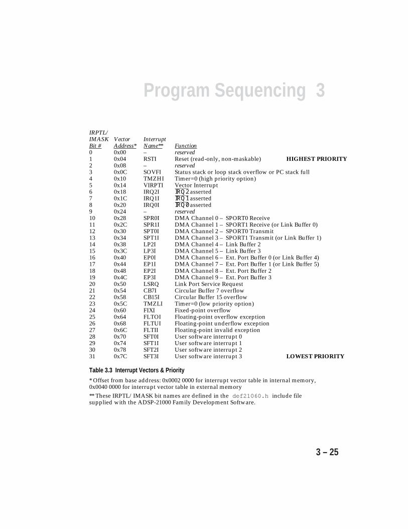
3Program Sequencing
3 – 25
IRPTL/IMASK Vector InterruptBit # Address* Name** Function0 0x00 – reserved1 0x04 RSTI Reset (read-only, non-maskable) HIGHEST PRIORITY2 0x08 – reserved3 0x0C SOVFI Status stack or loop stack overflow or PC stack full4 0x10 TMZHI Timer=0 (high priority option)5 0x14 VIRPTI Vector Interrupt6 0x18 IRQ2I IRQ2 asserted7 0x1C IRQ1I IRQ1 asserted8 0x20 IRQ0I IRQ0 asserted9 0x24 – reserved10 0x28 SPR0I DMA Channel 0 – SPORT0 Receive11 0x2C SPR1I DMA Channel 1 – SPORT1 Receive (or Link Buffer 0)12 0x30 SPT0I DMA Channel 2 – SPORT0 Transmit13 0x34 SPT1I DMA Channel 3 – SPORT1 Transmit (or Link Buffer 1)14 0x38 LP2I DMA Channel 4 – Link Buffer 215 0x3C LP3I DMA Channel 5 – Link Buffer 316 0x40 EP0I DMA Channel 6 – Ext. Port Buffer 0 (or Link Buffer 4)17 0x44 EP1I DMA Channel 7 – Ext. Port Buffer 1 (or Link Buffer 5)18 0x48 EP2I DMA Channel 8 – Ext. Port Buffer 219 0x4C EP3I DMA Channel 9 – Ext. Port Buffer 320 0x50 LSRQ Link Port Service Request21 0x54 CB7I Circular Buffer 7 overflow22 0x58 CB15I Circular Buffer 15 overflow23 0x5C TMZLI Timer=0 (low priority option)24 0x60 FIXI Fixed-point overflow25 0x64 FLTOI Floating-point overflow exception26 0x68 FLTUI Floating-point underflow exception27 0x6C FLTII Floating-point invalid exception28 0x70 SFT0I User software interrupt 029 0x74 SFT1I User software interrupt 130 0x78 SFT2I User software interrupt 231 0x7C SFT3I User software interrupt 3 LOWEST PRIORITY
Table 3.3 Interrupt Vectors & Priority
* Offset from base address: 0x0002 0000 for interrupt vector table in internal memory,0x0040 0000 for interrupt vector table in external memory** These IRPTL/IMASK bit names are defined in the def21060.h include filesupplied with the ADSP-21000 Family Development Software.
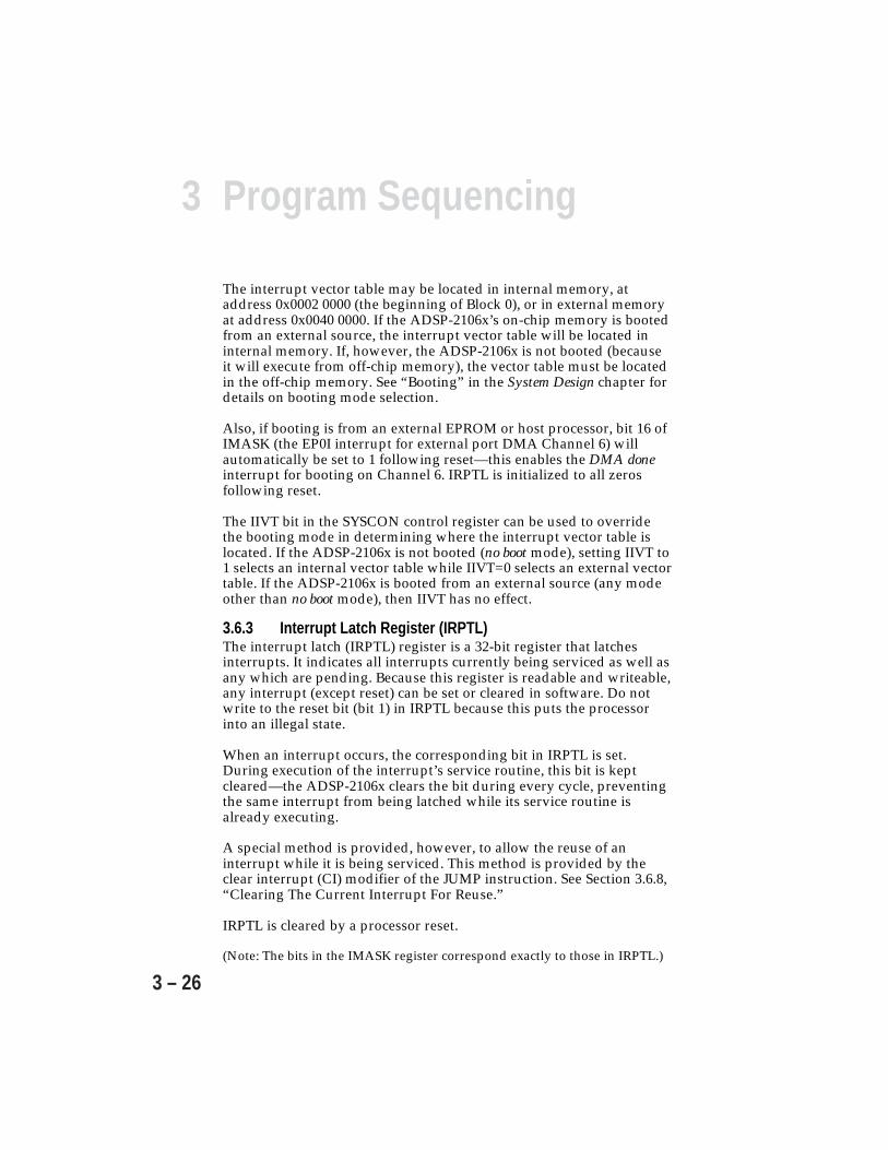
3 Program Sequencing
3 – 26
The interrupt vector table may be located in internal memory, ataddress 0x0002 0000 (the beginning of Block 0), or in external memoryat address 0x0040 0000. If the ADSP-2106x’s on-chip memory is bootedfrom an external source, the interrupt vector table will be located ininternal memory. If, however, the ADSP-2106x is not booted (becauseit will execute from off-chip memory), the vector table must be locatedin the off-chip memory. See “Booting” in the System Design chapter fordetails on booting mode selection.
Also, if booting is from an external EPROM or host processor, bit 16 ofIMASK (the EP0I interrupt for external port DMA Channel 6) willautomatically be set to 1 following reset—this enables the DMA doneinterrupt for booting on Channel 6. IRPTL is initialized to all zerosfollowing reset.
The IIVT bit in the SYSCON control register can be used to overridethe booting mode in determining where the interrupt vector table islocated. If the ADSP-2106x is not booted (no boot mode), setting IIVT to1 selects an internal vector table while IIVT=0 selects an external vectortable. If the ADSP-2106x is booted from an external source (any modeother than no boot mode), then IIVT has no effect.
3.6.3 Interrupt Latch Register (IRPTL)The interrupt latch (IRPTL) register is a 32-bit register that latchesinterrupts. It indicates all interrupts currently being serviced as well asany which are pending. Because this register is readable and writeable,any interrupt (except reset) can be set or cleared in software. Do notwrite to the reset bit (bit 1) in IRPTL because this puts the processorinto an illegal state.
When an interrupt occurs, the corresponding bit in IRPTL is set.During execution of the interrupt’s service routine, this bit is keptcleared—the ADSP-2106x clears the bit during every cycle, preventingthe same interrupt from being latched while its service routine isalready executing.
A special method is provided, however, to allow the reuse of aninterrupt while it is being serviced. This method is provided by theclear interrupt (CI) modifier of the JUMP instruction. See Section 3.6.8,“Clearing The Current Interrupt For Reuse.”
IRPTL is cleared by a processor reset.
(Note: The bits in the IMASK register correspond exactly to those in IRPTL.)
3Program Sequencing
3 – 27
3.6.4 Interrupt PriorityThe interrupt bits in IRPTL are ordered by priority. The interruptpriority is from 0 (highest) to 31 (lowest). Interrupt priority determineswhich interrupt is serviced first when more than one occurs in thesame cycle. It also determines which interrupts are nested whennesting is enabled (see “Interrupt Nesting and IMASKP”).
The arithmetic interrupts—fixed-point overflow and floating-pointoverflow, underflow, and invalid operation—are determined fromflags in the sticky status register (STKY). By reading these flags, theservice routine for one of these interrupts can determine whichcondition caused the interrupt. The routine also has to clear theappropriate STKY bit so that the interrupt is not still active after theservice routine is done.
The timer decrementing to zero causes both interrupt 4 and interrupt14. This feature allows you to choose the priority of the timer interrupt.Unmask the timer interrupt that has the priority you want, and leavethe other one masked. Unmasking both interrupts results in twointerrupts when the timer reaches zero. In this case the processorservices the higher priority interrupt first, then the lower priorityinterrupt.
3.6.5 Interrupt Masking & ControlAll interrupts except for reset can be enabled and disabled by theglobal interrupt enable bit, IRPTEN, bit 12 in the MODE1 register. Thisbit is cleared at reset. You must set this bit for interrupts to be enabled.
3.6.5.1 Interrupt Mask Register (IMASK)All interrupts except for reset can be masked. Masked means theinterrupt is disabled. Interrupts that are masked are still latched (inIRPTL), so that if the interrupt is later unmasked, it is processed.
The IMASK register controls interrupt masking. The bits in IMASKcorrespond exactly to the bits in the IRPTL register. For example, bit 10in IMASK masks or unmasks the same interrupt latched by bit 10 inIRPTL.
– If a bit in IMASK is set to 1, its interrupt is unmasked (enabled).– If the bit is cleared (to 0), the interrupt is masked (disabled).

3 Program Sequencing
3 – 28
After reset, all interrupts except for the reset interrupt and theEP0I interrupt for external port DMA Channel 6 (bit 16 of IMASK) aremasked. The reset interrupt is always non-maskable. The EP0Iinterrupt is automatically unmasked after reset if the ADSP-2106x isbooting from EPROM or from a host.
3.6.5.2 Interrupt Nesting & IMASKPThe ADSP-2106x supports the nesting of one interrupt service routineinside another; that is, a service routine can be interrupted by a higherpriority interrupt. This feature is controlled by the nesting mode bit(NESTM) in the MODE1 register.
When the NESTM bit is a 0, an interrupt service routine cannot beinterrupted; any interrupt that occurs will be processed only after theroutine finishes. When NESTM is a 1, higher priority interrupts caninterrupt if they are not masked; lower or equal priority interruptscannot. The NESTM bit should only be changed outside of an interruptservice routine or during the reset service routine; otherwise, interruptnesting may not work correctly.
If nesting is enabled and a higher priority interrupt occursimmediately after a lower priority interrupt, the service routine of thehigher priority interrupt is delayed by one cycle. This allows the firstinstruction of the lower priority interrupt routine to be executed beforeit is interrupted.
In nesting mode, the ADSP-2106x uses the interrupt mask pointer(IMASKP) to create a temporary interrupt mask for each level ofinterrupt nesting; the IMASK value is not affected. The ADSP-2106xchanges IMASKP each time a higher priority interrupt interrupts alower priority service routine.
The bits in IMASKP correspond to the interrupts in order of priority,the same as in IRPTL and IMASK. When an interrupt occurs, its bit isset in IMASKP. If nesting is enabled, a new temporary interrupt maskis generated by masking all interrupts of equal or lower priority to thehighest priority bit set in IMASKP (and keeping higher priorityinterrupts the same as in IMASK). When a return from an interruptservice routine (RTI) is executed, the highest priority bit set in IMASKPis cleared, and again a new temporary interrupt mask is generated bymasking all interrupts of equal or lower priority to the highest prioritybit set in IMASKP. The bit set in IMASKP that has the highest priorityalways corresponds to the priority of the interrupt being serviced.
3Program Sequencing
3 – 29
If nesting is not enabled, the processor masks out all interrupts andIMASKP is not used, although IMASKP is still updated to create atemporary interrupt mask.
IRPTL is updated, but the ADSP-2106x does not vector to an interruptthat occurs while its service routine is already executing. It waits untilthe RTI completes before vectoring to the service routine again.
3.6.6 Status Stack Save & RestoreFor low-overhead interrupt servicing, the ADSP-2106x automaticallysaves and restores the status and mode contexts of the interruptedprogram. The three external interrupts (IRQ2-0), the timer interrupt,and the VIRPT vector interrupt cause an automatic push of ASTATand MODE1 onto the status stack, which is five levels deep. Theseregisters are automatically popped from the status stack by the returnfrom interrupt instruction, RTI (and by the JUMP (CI) instruction,described below in “Clearing The Current Interrupt For Reuse”).
Only IRQ2-0, timer, and VIRPT interrupts cause a push of thestatus stack. All other interrupts require an explicit save andrestore of the appropriate registers to memory.
Pushing ASTAT and MODE1 preserves the status and control bitsettings so that if the service routine alters these bits, the originalsettings are automatically restored upon the return from interrupt.
Note, however, that the FLAG3-0 bits in ASTAT are not affected bystatus stack pushes and pops; the values of these bits carry over fromthe main program to the service routine and from the service routineback to the main program.
The top of the status stack contains the current values of ASTAT andMODE1. Reading and writing these registers does not move the stackpointer. The stack pointer is moved, however, by explicit PUSH andPOP instructions.
3.6.7 Software InterruptsThe ADSP-2106x provides software interrupts that emulate interruptbehavior but are activated through software instead of hardware.Setting one of bits 28-31 in IRPTL, with either a BIT SET instruction ora write to IRPTL, activates a software interrupt. The ADSP-2106xbranches to the corresponding interrupt routine if that interrupt is notmasked and interrupts are enabled.
3 Program Sequencing
3 – 30
3.6.8 Clearing The Current Interrupt For ReuseNormally the ADSP-2106x ignores and does not latch an interrupt thatreoccurs while its service routine is already executing. When theinterrupt initially occurs, the corresponding bit in IRPTL is set. Duringexecution of the service routine, this bit is kept cleared—theADSP-2106x clears the bit during every cycle, preventing the sameinterrupt from being latched while its service routine is alreadyexecuting.
The clear interrupt (CI) modifier of the JUMP instruction, however,allows the reuse of an interrupt while it is being serviced. This can beuseful in systems that require fast interrupt response and low interruptlatency. The JUMP (CI) instruction should be located within theinterrupt service routine. JUMP (CI) clears the status of the currentinterrupt without leaving the interrupt service routine, reducing theinterrupt routine to a normal subroutine—this allows the interrupt tooccur again, as a result of a different event or task in the ADSP-2106xsystem.
The JUMP (CI) instruction reduces an interrupt service routine to anormal subroutine by clearing the appropriate bit in the interrupt latchregister (IRPTL) and interrupt mask pointer (IMASKP) and poppingthe status stack. The ADSP-2106x then stops automatically clearing theinterrupt’s latch bit (in IRPTL) in every cycle, allowing the interrupt tooccur again.
When returning from a subroutine which has been reduced from aninterrupt service routine with a JUMP (CI) instruction, the (LR)modifier of the RTS instruction must be used (in case the interruptoccurred during the last two instructions of a loop). Refer to “GeneralRestrictions” in Section 3.5, “Loops”, for a description of the RTS (LR)instruction.
The following example shows an interrupt service routine that isreduced to a subroutine with the (CI) modifier:
instr1; interrupt entry from main programJUMP(PC,3) (DB,CI); clear interrupt statusinstr3;instr4;instr5;RTS (LR); use LR modifier with return from subroutine
3Program Sequencing
3 – 31
Note that the JUMP(PC,3)(DB,CI) instruction actually onlycontinues linear execution flow by jumping to the location PC + 3(instr5), with the two intervening instructions (instr3, instr4) beingexecuted because of the delayed branch (DB). This JUMP instruction isonly an example—a JUMP (CI) can be to any location.
3.6.9 External Interrupt Timing & SensitivityEach of the ADSP-2106x’s three external interrupts, IRQ2-0, can beeither level- or edge-triggered.
The ADSP-2106x samples interrupts once every CLKIN cycle. Level-sensitive interrupts are considered valid if sampled active (low). Alevel-sensitive interrupt must go inactive (high) before the processorreturns from the interrupt service routine. If a level-sensitive interruptis still active when the processor samples it, the processor treats it as anew request, repeating the same interrupt routine without returning tothe main program (assuming no higher priority interrupts are active).
Edge-triggered interrupt requests are considered valid if sampled highin one cycle and low in the next. The interrupt can stay activeindefinitely. To request another interrupt, the signal must go high,then low again.
Edge-triggered interrupts require less external hardware compared tolevel-sensitive requests since there is never a need to negate therequest. However, multiple interrupting devices may share a singlelevel-sensitive request line on a wired-OR basis, which allows for easysystem expansion.
A bit for each interrupt in the MODE2 register indicates the sensitivitymode of each interrupt.
MODE2Bit Name Definition0 IRQ0E 1=edge-sensitive; 0=level-sensitive1 IRQ1E 1=edge-sensitive; 0=level-sensitive2 IRQ2E 1=edge-sensitive; 0=level-sensitive
3 Program Sequencing
3 – 32
3.6.9.1 Asynchronous External InterruptsThe processor accepts interrupts that are asynchronous to the ADSP-2106x clock; that is, an interrupt signal may change at any time. Anasynchronous interrupt must be held low at least one CLKIN cycle toguarantee that it is sampled. Synchronous interrupts need only meetthe setup and hold time requirements relative to the rising edge ofCLKIN, as specified in the ADSP-2106x Data Sheet.
3.6.10 Multiprocessor Vector Interrupts (VIRPT)Vector interrupts are used for interprocessor commands in multiple-processor systems. When an external processor writes an address tothe VIRPT register a vector interrupt is caused. The external processormay be either another ADSP-2106x or a host.
When the vector interrupt is serviced, the ADSP-2106x automaticallypushes the status stack and begins executing the service routinelocated at the address specified in VIRPT. The lower 24 bits of VIRPTcontain the address; the upper 8 bits may be optionally used as data tobe read by the interrupt service routine. At reset, VIRPT is initialized toits standard address in the ADSP-2106x’s interrupt vector table.
The minimum latency for vector interrupts is six cycles, five of whichare NOPs. When the RTI (return from interrupt) instruction is reachedin the service routine, the ADSP-2106x automatically pops the statusstack.
The VIPD bit in SYSTAT reflects the status of the VIRPT register. IfVIRPT is written while a previous vector interrupt is pending, the newvector address replaces the pending one. If VIRPT is written while aprevious vector interrupt is being serviced, the new vector address isignored and no new interrupt is triggered. If the ADSP-2106x writes toits own VIRPT register it is ignored.
To use the ADSP-2106x’s vector interrupt feature, external processorscan take the following sequence of actions:
1. Poll the VIRPT register until it reads a certain token value (i.e. zero).2. Write the vector interrupt service routine address to VIRPT.3. When the service routine is finished, it writes the token back into
VIRPT to indicate that it is finished and that another vector interruptcan be initiated.
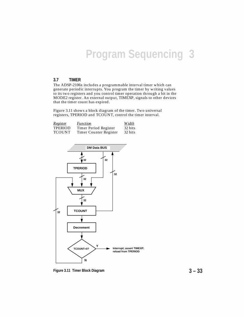
3Program Sequencing
3 – 33
3.7 TIMERThe ADSP-2106x includes a programmable interval timer which cangenerate periodic interrupts. You program the timer by writing valuesto its two registers and you control timer operation through a bit in theMODE2 register. An external output, TIMEXP, signals to other devicesthat the timer count has expired.
Figure 3.11 shows a block diagram of the timer. Two universalregisters, TPERIOD and TCOUNT, control the timer interval.
Register Function WidthTPERIOD Timer Period Register 32 bitsTCOUNT Timer Counter Register 32 bits
TPERIOD
TCOUNT
MUX
Decrement
DM Data BUS
Interrupt; assert TIMEXP;reload from TPERIOD
32
32
32
32
32
32
TCOUNT=0?Y
N
Figure 3.11 Timer Block Diagram
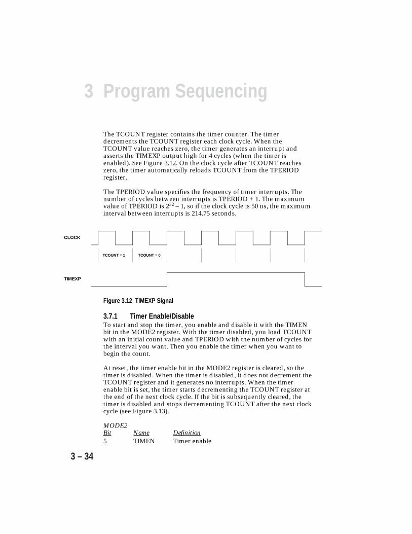
3 Program Sequencing
3 – 34
The TCOUNT register contains the timer counter. The timerdecrements the TCOUNT register each clock cycle. When theTCOUNT value reaches zero, the timer generates an interrupt andasserts the TIMEXP output high for 4 cycles (when the timer isenabled). See Figure 3.12. On the clock cycle after TCOUNT reacheszero, the timer automatically reloads TCOUNT from the TPERIODregister.
The TPERIOD value specifies the frequency of timer interrupts. Thenumber of cycles between interrupts is TPERIOD + 1. The maximumvalue of TPERIOD is 232 – 1, so if the clock cycle is 50 ns, the maximuminterval between interrupts is 214.75 seconds.
CLOCK
TCOUNT = 1 TCOUNT = 0
TIMEXP
Figure 3.12 TIMEXP Signal
3.7.1 Timer Enable/DisableTo start and stop the timer, you enable and disable it with the TIMENbit in the MODE2 register. With the timer disabled, you load TCOUNTwith an initial count value and TPERIOD with the number of cycles forthe interval you want. Then you enable the timer when you want tobegin the count.
At reset, the timer enable bit in the MODE2 register is cleared, so thetimer is disabled. When the timer is disabled, it does not decrement theTCOUNT register and it generates no interrupts. When the timerenable bit is set, the timer starts decrementing the TCOUNT register atthe end of the next clock cycle. If the bit is subsequently cleared, thetimer is disabled and stops decrementing TCOUNT after the next clockcycle (see Figure 3.13).
MODE2Bit Name Definition5 TIMEN Timer enable
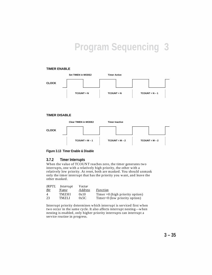
3Program Sequencing
3 – 35
CLOCK
Set TIMEN in MODE2
TCOUNT = N TCOUNT = N TCOUNT = N – 1
CLOCK
Clear TIMEN in MODE2
TCOUNT = M – 1 TCOUNT = M – 2 TCOUNT = M – 2
Timer Active
Timer Inactive
TIMER DISABLE
TIMER ENABLE
Figure 3.13 Timer Enable & Disable
3.7.2 Timer InterruptsWhen the value of TCOUNT reaches zero, the timer generates twointerrupts, one with a relatively high priority, the other with arelatively low priority. At reset, both are masked. You should unmaskonly the timer interrupt that has the priority you want, and leave theother masked.
IRPTL Interrupt VectorBit Name Address Function4 TMZHI 0x10 Timer =0 (high priority option)23 TMZLI 0x5C Timer=0 (low priority option)
Interrupt priority determines which interrupt is serviced first whentwo occur in the same cycle. It also affects interrupt nesting—whennesting is enabled, only higher priority interrupts can interrupt aservice routine in progress.
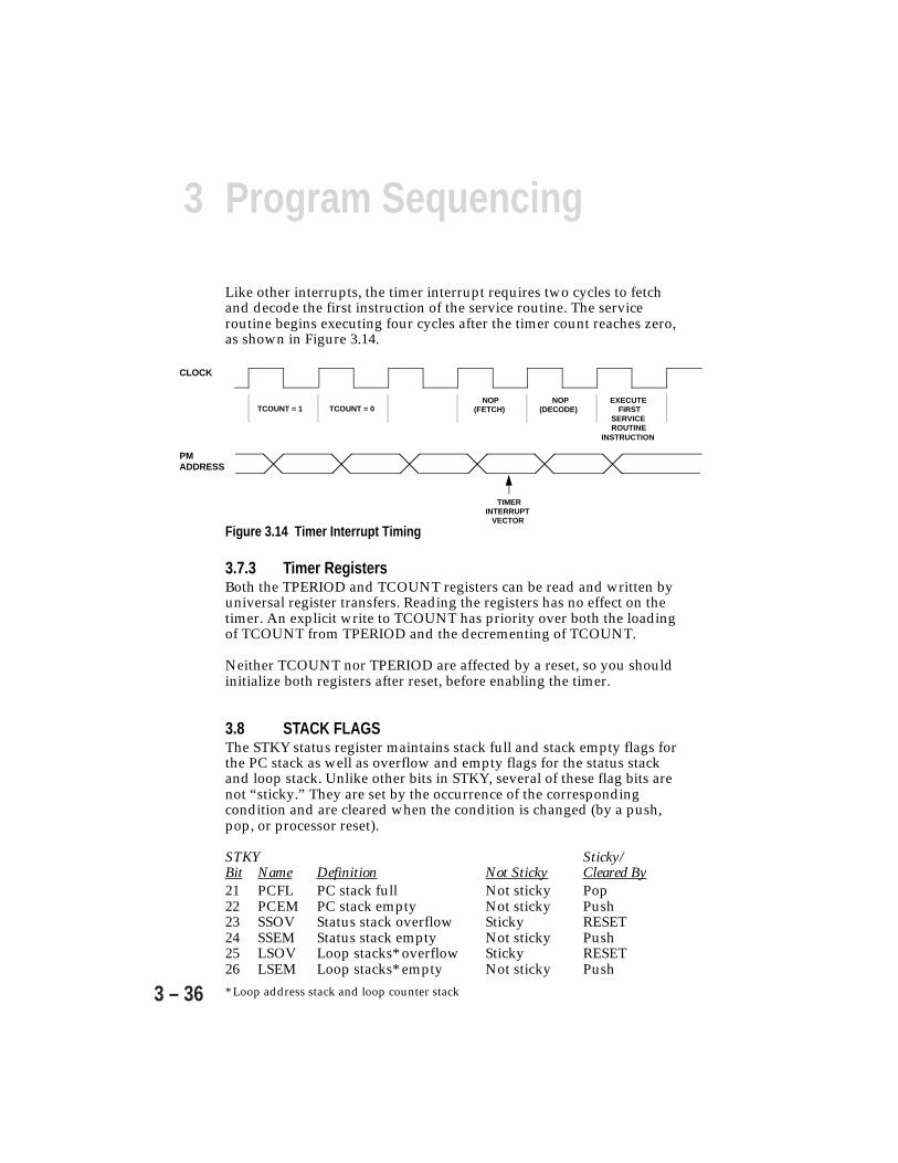
3 Program Sequencing
3 – 36
Like other interrupts, the timer interrupt requires two cycles to fetchand decode the first instruction of the service routine. The serviceroutine begins executing four cycles after the timer count reaches zero,as shown in Figure 3.14.
CLOCK
TCOUNT = 1 TCOUNT = 0
PM ADDRESS
NOP(FETCH)
NOP(DECODE)
EXECUTEFIRST
SERVICEROUTINE
INSTRUCTION
TIMERINTERRUPT
VECTOR
Figure 3.14 Timer Interrupt Timing
3.7.3 Timer RegistersBoth the TPERIOD and TCOUNT registers can be read and written byuniversal register transfers. Reading the registers has no effect on thetimer. An explicit write to TCOUNT has priority over both the loadingof TCOUNT from TPERIOD and the decrementing of TCOUNT.
Neither TCOUNT nor TPERIOD are affected by a reset, so you shouldinitialize both registers after reset, before enabling the timer.
3.8 STACK FLAGSThe STKY status register maintains stack full and stack empty flags forthe PC stack as well as overflow and empty flags for the status stackand loop stack. Unlike other bits in STKY, several of these flag bits arenot “sticky.” They are set by the occurrence of the correspondingcondition and are cleared when the condition is changed (by a push,pop, or processor reset).
STKY Sticky/Bit Name Definition Not Sticky Cleared By21 PCFL PC stack full Not sticky Pop22 PCEM PC stack empty Not sticky Push23 SSOV Status stack overflow Sticky RESET24 SSEM Status stack empty Not sticky Push25 LSOV Loop stacks* overflow Sticky RESET26 LSEM Loop stacks* empty Not sticky Push* Loop address stack and loop counter stack
3Program Sequencing
3 – 37
The status stack flags are read-only. Writes to the STKY register haveno effect on these bits.
The overflow and full flags are provided for diagnostic aid only andare not intended to allow recovery from overflow. Status stack or loopstack overflow or PC stack full causes an interrupt.
The empty flags facilitate stack saves to memory. You monitor theempty flag when saving a stack to memory to know when all valueshave been transferred. The empty flags do not cause interrupts becausean empty stack is an acceptable condition.
3.9 IDLE & IDLE16IDLE and IDLE16 are special instructions that halt the ADSP-2106xcore processor in a low-power state until an external interrupt (IRQ2-0),timer interrupt, DMA interrupt, or VIRPT vector interrupt occurs.When the processor executes an IDLE instruction, it fetches one moreinstruction at the current fetch address and then suspends operation.The ADSP-2106x’s I/O processor is unaffected by the IDLEinstruction—any DMA transfers to or from internal memory willcontinue uninterrupted.
The processor’s internal clock continues to run during IDLE, as well asthe timer (if it is enabled). When an external interrupt (IRQ2-0), timerinterrupt, DMA interrupt, or VIRPT vector interrupt occurs, theprocessor responds normally. After two cycles needed to fetch anddecode the first instruction of the interrupt service routine, theprocessor continues executing instructions normally.
On the ADSP-21061 only, the IDLE16 instruction executes a NOP and putsthe processor in a low power state. IDLE16 is a lower power version of theIDLE instruction. This instruction halts the processor like the IDLEinstruction; in this case, the internal clock runs at 1/16th the rate ofCLKIN. The ADSP-21061's I/O processor continues to function, but alloperations occur at 1/16th the rate. All internal memory transfers requirean extra 15 cycles. The serial clocks and frame syncs (if being sourced bythe ADSP-21061) are divided down by a factor of 16 during IDLE16.Similarly, all Host accesses take 16 times longer to complete. Theprocessor remains in the low power state until an interrupt occurs.
After returning from the interrupt, execution continues at theinstruction following the IDLE or IDLE16 instruction.

3 Program Sequencing
3 – 38
3.10 INSTRUCTION CACHEThe ADSP-2106x’s on-chip instruction cache is a 2-way, set-associativecache with entries for 32 instructions. Operation of the cache istransparent to the programmer. The ADSP-2106x caches onlyinstructions that conflict with program memory data accesses (over thePM Data Bus, with the address generated by DAG2 on thePM Address Bus). This feature makes the cache considerably moreefficient than a cache that loads every instruction, since typically only afew instructions must access data from a block of program memory.
Because of the three-stage instruction pipeline, if the instruction ataddress n requires a program memory data access, there is a conflictwith the instruction fetch at address n+2, assuming sequentialexecution. It is this fetched instruction (n+2) that is stored in theinstruction cache, not the instruction requiring the program memorydata access.
If the instruction needed is in the cache, a “cache hit” occurs—thecache provides the instruction while the program memory data accessis performed. If the instruction needed is not in the cache, a “cachemiss” occurs, and the instruction fetch (from memory) takes place inthe cycle following the program memory data access, incurring onecycle of overhead. This instruction is loaded into the cache, if the cacheis enabled and not frozen, so that it is available the next time the sameinstruction (requiring program memory data) is executed.
3.10.1 Cache ArchitectureFigure 3.15 shows a block diagram of the instruction cache. The cachecontains 32 entries. An entry consists of a register pair containing aninstruction and its address. Each entry has a “valid” bit which is set ifthe entry contains a valid instruction.
The entries are divided into 16 sets (numbered 15-0) of two entrieseach, entry 0 and entry 1. Each set has an LRU (Least Recently Used)bit whose value indicates which of the two entries contains the leastrecently used instruction (1=entry 1, 0=entry 0).
Every possible instruction address is mapped to a set in the cache byits 4 LSBs. When the processor needs to fetch an instruction from thecache, it uses the 4 address LSBs as an index to a particular set. Within
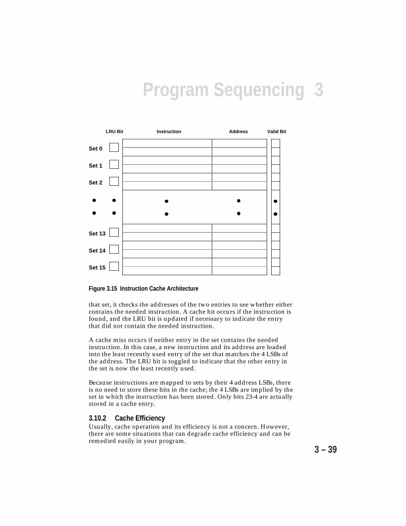
3Program Sequencing
3 – 39
Set 0
Set 1
Set 2
Set 13
Set 14
Set 15
LRU Bit Valid BitInstruction Address
Figure 3.15 Instruction Cache Architecture
that set, it checks the addresses of the two entries to see whether eithercontains the needed instruction. A cache hit occurs if the instruction isfound, and the LRU bit is updated if necessary to indicate the entrythat did not contain the needed instruction.
A cache miss occurs if neither entry in the set contains the neededinstruction. In this case, a new instruction and its address are loadedinto the least recently used entry of the set that matches the 4 LSBs ofthe address. The LRU bit is toggled to indicate that the other entry inthe set is now the least recently used.
Because instructions are mapped to sets by their 4 address LSBs, thereis no need to store these bits in the cache; the 4 LSBs are implied by theset in which the instruction has been stored. Only bits 23-4 are actuallystored in a cache entry.
3.10.2 Cache EfficiencyUsually, cache operation and its efficiency is not a concern. However,there are some situations that can degrade cache efficiency and can beremedied easily in your program.
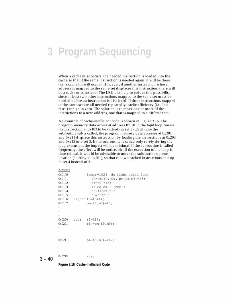
3 Program Sequencing
3 – 40
When a cache miss occurs, the needed instruction is loaded into thecache so that if the same instruction is needed again, it will be there(i.e. a cache hit will occur). However, if another instruction whoseaddress is mapped to the same set displaces this instruction, there willbe a cache miss instead. The LRU bits help to reduce this possibilitysince at least two other instructions mapped to the same set must beneeded before an instruction is displaced. If three instructions mappedto the same set are all needed repeatedly, cache efficiency (i.e. “hitrate”) can go to zero. The solution is to move one or more of theinstructions to a new address, one that is mapped to a different set.
An example of cache-inefficient code is shown in Figure 3.16. Theprogram memory data access at address 0x101 in the tight loop causesthe instruction at 0x103 to be cached (in set 3). Each time thesubroutine sub is called, the program memory data accesses at 0x201and 0x211 displace this instruction by loading the instructions at 0x203and 0x213 into set 3. If the subroutine is called only rarely during theloop execution, the impact will be minimal. If the subroutine is calledfrequently, the effect will be noticeable. If the execution of the loop istime-critical, it would be advisable to move the subroutine up onelocation (starting at 0x201), so that the two cached instructions end upin set 4 instead of 3.
Address0x0100 lcntr=1024, do tight until lce;0x0101 r0=dm(i0,m0), pm(i8,m8)=f3;0x0102 r1=r0-r15;0x0103 if eq call (sub);0x0104 f2=float r1;0x0105 f3=f2*f2;0x0106 tight: f3=f3+f4;0x0107 pm(i8,m8)=f3;•••0x0200 sub: r1=R13;0x0201 r14=pm(i9,m9);•••0x0211 pm(i9,m9)=r12;•••0x021F rts;
Figure 3.16 Cache-Inefficient Code
3Program Sequencing
3 – 41
3.10.3 Cache Disable & Cache FreezeFreezing the cache prevents any changes to its contents—a cache misswill not result in a new instruction being stored in the cache. Disablingthe cache stops its operation completely; all instruction fetchesconflicting with program memory data accesses are delayed by theaccess. These functions are selected by the CADIS (cache enable/disable) and CAFRZ (cache freeze) bits in the MODE2 register:
MODE2Bit Name Function4 CADIS Cache Disable19 CAFRZ Cache Freeze
After reset the cache is cleared, containing no instructions, and isunfrozen and enabled.
An instruction containing a program memory data access must not beplaced directly after a cache enable or cache disable instruction—theADSP-2106x must wait at least one cycle before executing the PM dataaccess. A NOP may be inserted to accomplish this.

3 Program Sequencing
3 – 42
4Data Addressing
4 – 1
4.1 OVERVIEWThe ADSP-2106x’s two data address generators (DAGs) simplify the task oforganizing data by maintaining pointers into memory. The DAGs allow theprocessor to address memory indirectly; that is, an instruction specifies aDAG register containing an address instead of the address value itself.
Data address generator 1 (DAG1) generates 32-bit addresses on theDM Address Bus. Data address generator 2 (DAG2) generates 24-bitaddresses on the PM Address Bus. The basic architecture for both DAGsis shown in Figure 4.1 on the following page.
The DAGs also support in hardware some functions commonly used indigital signal processing algorithms. Both DAGs support circular databuffers, which require advancing a pointer repetitively through a range ofmemory. Both DAGs can also perform a bit-reversing operation, whichoutputs the bits of an address in reversed order.
4.2 DAG REGISTERSEach DAG has four types of registers: Index (I), Modify (M), Base (B), andLength (L) registers.
An I register acts as a pointer to memory, and an M register contains theincrement value for advancing the pointer. By modifying an I register withdifferent M values, you can vary the increment as needed.
B registers and L registers are used only for circular data buffers. AB register holds the base address (i.e. the first address) of a circular buffer.The same-numbered L register contains the number of locations in (i.e. thelength of) the circular buffer.
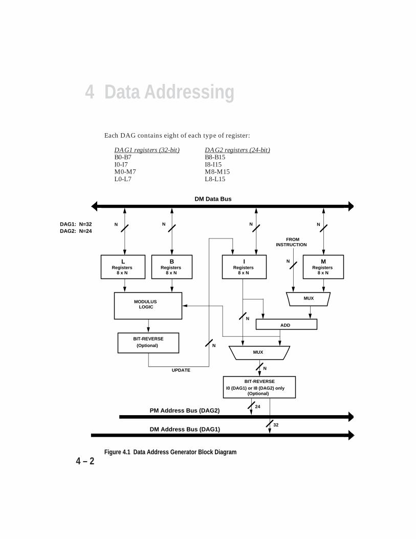
4 Data Addressing
4 – 2
Each DAG contains eight of each type of register:
DAG1 registers (32-bit) DAG2 registers (24-bit)B0-B7 B8-B15I0-I7 I8-I15M0-M7 M8-M15L0-L7 L8-L15
LRegisters
8 x N
DM Data Bus
ADD
IRegisters
8 x N
MRegisters
8 x N
MODULUSLOGIC
N N
N
FROMINSTRUCTION
BRegisters
8 x N
MUX
MUX
N N
BIT-REVERSE
(Optional)
N
UPDATE
N
N
DAG1: N=32DAG2: N=24
BIT-REVERSE
I0 (DAG1) or I8 (DAG2) only (Optional)
24
DM Address Bus (DAG1)
PM Address Bus (DAG2)
32
Figure 4.1 Data Address Generator Block Diagram

4Data Addressing
4 – 3
4.2.1 Alternate DAG RegistersEach DAG register has an alternate (secondary) register for contextswitching. For activating alternate registers, each DAG is organized intohigh and low halves, as shown in Figure 4.2. The high half of DAG1contains the I, M, B and L registers numbered 4-7, and the low half, theregisters numbered 0-3. Likewise, the high half of DAG2 consists ofregisters 12-15, and the low half consists of registers 8-11.
I0
I1
I2I3
I4I5
I6
I7
I8I9
I10
I11
I12
I13
I15
I14
M0
M1
M2M3
M4M5
M6
M7
M8M9
M10
M11
M12
M13
M15
M14
L0
L1
L2L3
L4L5
L6
L7
L8L9
L10
L11
L12
L13
L15
L14
B0
B1
B2B3
B4B5
B6
B7
B8B9
B10
B11
B12
B13
B15
B14
DAG1 Registers (Data Memory)
DAG2 Registers (Program Memory)
SRD1H
SRD1L
SRD2H
SRD2L
MODE1Select Bit
Figure 4.2 Alternate DAG Registers

4 Data Addressing
4 – 4
Several control bits in the MODE1 register determine for each halfwhether primary or alternate registers are active (0=primary registers,1=alternate registers):
MODE1Bit Name Definition3 SRD1H DAG1 alternate register select (4-7)4 SRD1L DAG1 alternate register select (0-3)5 SRD2H DAG2 alternate register select (12-15)6 SRD2L DAG2 alternate register select (8-11)
This grouping of alternate registers lets you pass pointers betweencontexts in each DAG.
4.3 DAG OPERATIONDAG operations include:
• address output with pre-modify or post-modify,• modulo addressing (for circular buffers), and• bit-reversed addressing
Short word addresses (for 16-bit data) are right-shifted by one bit beforebeing output onto the DM Address Bus. This allows internal memory touse the address directly. (See “16-Bit Short Words” in the Memory chapterof this manual for details on short word addresses.)
4.3.1 Address Output & ModificationThe processor can add an offset (modifier), either an M register or animmediate value, to an I register and output the resulting address; this iscalled a pre-modify without update operation. Or it can output the I registervalue as it is, and then add an M register or immediate value to form anew I register value. This is a post-modify operation. These operations arecompared in Figure 4.3. The pre-modify operation does not change thevalue of the I register. The width of an immediate modifier depends onthe instruction; it can be as large as the width of the I register. The Lregister and modulo logic do not affect a pre-modified address—pre-modify addressing is always linear, not circular.
Pre-modify addressing operations must not change the memory space ofthe address; for example, pre-modification of an address in ADSP-2106xInternal Memory Space should not generate an address in ExternalMemory Space. Refer to the Memory chapter for information on theADSP-2106x memory map.
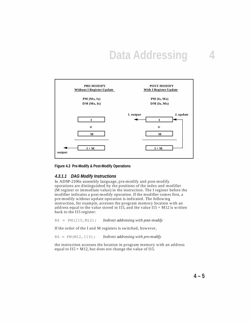
4Data Addressing
4 – 5
I
M
I
M
++
I + MI + M
1. output 2. update
output
PM (Mx, Ix) PM (Ix, Mx)
PRE-MODIFYWithout I Register Update
POST-MODIFY With I Register Update
DM (Ix, Mx)DM (Mx, Ix)
Figure 4.3 Pre-Modify & Post-Modify Operations
4.3.1.1 DAG Modify InstructionsIn ADSP-2106x assembly language, pre-modify and post-modifyoperations are distinguished by the positions of the index and modifier(M register or immediate value) in the instruction. The I register before themodifier indicates a post-modify operation. If the modifier comes first, apre-modify without update operation is indicated. The followinginstruction, for example, accesses the program memory location with anaddress equal to the value stored in I15, and the value I15 + M12 is writtenback to the I15 register:
R6 = PM(I15,M12); Indirect addressing with post-modify
If the order of the I and M registers is switched, however,
R6 = PM(M12,I15); Indirect addressing with pre-modify
the instruction accesses the location in program memory with an addressequal to I15 + M12, but does not change the value of I15.

4 Data Addressing
4 – 6
Any M register can modify any I register within the same DAG (DAG1 orDAG2). Thus,
DM(M0,I2) = TPERIOD;
is a legal instruction that accesses the data memory location M0 + I2;however,
DM(M0,I14) = TPERIOD;
is not a legal instruction because the I and M registers belong to differentDAGs.
4.3.1.2 Immediate ModifiersThe magnitude of an immediate value that can modify an I registerdepends on the instruction type and whether the I register is in DAG1 orDAG2. DAG1 modify values can be up to 32 bits wide; DAG2 modifyvalues can be up to 24 bits wide. Some instructions with paralleloperations only allow modify values up to 6 bits wide. Here are twoexamples:
32-bit modifier:
R1=DM(0x40000000,I1); DM address = I1 + 0x4000 0000
6-bit modifier:F6=F1+F2,PM(I8,0x0B)=ASTAT; PM address = I8, I8 = I8 + 0x0B
4.3.2 Circular Buffer AddressingThe DAGs provide for addressing of locations within a circular databuffer. A circular buffer is a set of memory locations that stores data. Anindex pointer steps through the buffer, being post-modified and updatedby the addition of a specified value (positive or negative) for each step. Ifthe modified address pointer falls outside the buffer, the length of thebuffer is subtracted from or added to the value, as required to wrap theindex pointer back to the start of the buffer (see Figure 4.4). There are norestrictions on the value of the base address for a circular buffer.
Circular buffer addressing must use M registers for post-modify of Iregisters, not pre-modify; for example:
F1=DM(I0,M0); Use post-modify addressing for circular buffers,F1=DM(M0,I0); not pre-modify.
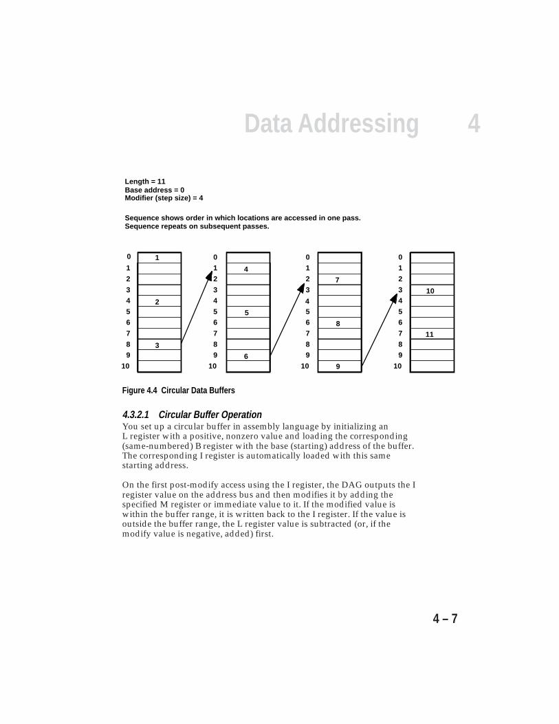
4Data Addressing
4 – 7
0
1
2
34
56
7
89
10
01
2
34
56
7
89
10
01
2
3
456
7
89
10
01
2
34
56
7
89
10
1
2
3
4
5
6
7
8
9
10
11
Length = 11Base address = 0Modifier (step size) = 4
Sequence shows order in which locations are accessed in one pass. Sequence repeats on subsequent passes.
Figure 4.4 Circular Data Buffers
4.3.2.1 Circular Buffer OperationYou set up a circular buffer in assembly language by initializing anL register with a positive, nonzero value and loading the corresponding(same-numbered) B register with the base (starting) address of the buffer.The corresponding I register is automatically loaded with this samestarting address.
On the first post-modify access using the I register, the DAG outputs the Iregister value on the address bus and then modifies it by adding thespecified M register or immediate value to it. If the modified value iswithin the buffer range, it is written back to the I register. If the value isoutside the buffer range, the L register value is subtracted (or, if themodify value is negative, added) first.
4 Data Addressing
4 – 8
If M is positive,
Inew = Iold + M if Iold + M < Buffer base + length (end of buffer)Inew = Iold + M – L if Iold + M ≥ Buffer base + length (end of buffer)
If M is negative,
Inew = Iold + M if Iold + M ≥ Buffer base (start of buffer)Inew = Iold + M + L if Iold + M < Buffer base (start of buffer)
4.3.2.2 Circular Buffer RegistersAll four types of DAG registers are involved in the operation of a circularbuffer:
• The I register contains the value which is output on the address bus.
• The M register contains the post-modify amount (positive or negative)which is added to the I register at the end of each memory access. TheM register can be any M register in the same DAG as the I register anddoes not have to have the same number. The modify value can also be animmediate number instead of an M register. The magnitude of themodify value, whether from an M register or immediate, must be lessthan the length (L register) of the circular buffer.
• The L register sets the size of the circular buffer and thus the addressrange that the I register is allowed to circulate through. L must bepositive and cannot have a value greater than 231 – 1 (for L0-L7) or223 – 1 (for L8-L15). If an L register’s value is zero, its circular bufferoperation is disabled.
• The B register, or the B register plus the L register, is the value that themodified I value is compared to after each access. When the B register isloaded, the corresponding I register is simultaneously loaded with thesame value. When I is loaded, B is not changed. B and I can be readindependently.
4.3.2.3 Circular Buffer Overflow InterruptsThere is one set of registers in each DAG that can generate an interrupt uponcircular buffer overflow (i.e. address wraparound). In DAG1, the registersare B7, I7, L7, and in DAG2 they are B15, I15, L15. Circular buffer overflowinterrupts can be used to implement a ping-pong (i.e. swap I/O bufferpointers) routine, for example.
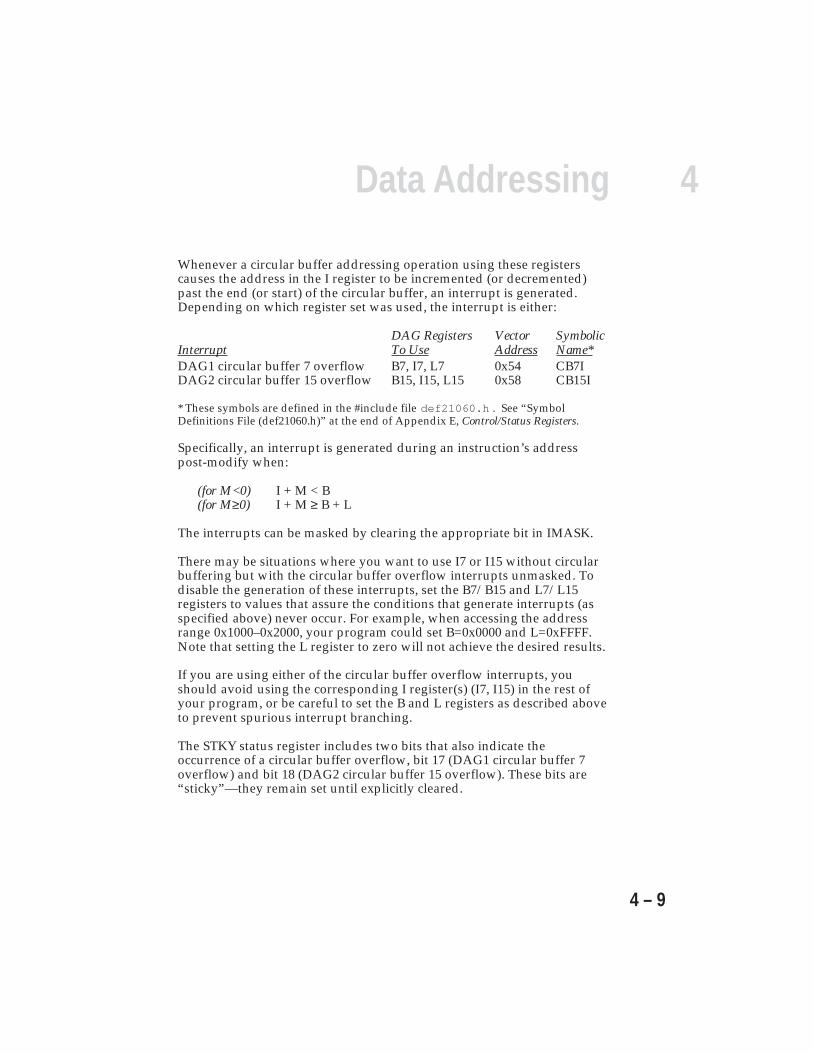
4Data Addressing
4 – 9
Whenever a circular buffer addressing operation using these registerscauses the address in the I register to be incremented (or decremented)past the end (or start) of the circular buffer, an interrupt is generated.Depending on which register set was used, the interrupt is either:
DAG Registers Vector SymbolicInterrupt To Use Address Name*DAG1 circular buffer 7 overflow B7, I7, L7 0x54 CB7IDAG2 circular buffer 15 overflow B15, I15, L15 0x58 CB15I
* These symbols are defined in the #include file def21060.h . See “SymbolDefinitions File (def21060.h)” at the end of Appendix E, Control/Status Registers.
Specifically, an interrupt is generated during an instruction’s addresspost-modify when:
(for M<0) I + M < B(for M≥0) I + M ≥ B + L
The interrupts can be masked by clearing the appropriate bit in IMASK.
There may be situations where you want to use I7 or I15 without circularbuffering but with the circular buffer overflow interrupts unmasked. Todisable the generation of these interrupts, set the B7/B15 and L7/L15registers to values that assure the conditions that generate interrupts (asspecified above) never occur. For example, when accessing the addressrange 0x1000–0x2000, your program could set B=0x0000 and L=0xFFFF.Note that setting the L register to zero will not achieve the desired results.
If you are using either of the circular buffer overflow interrupts, youshould avoid using the corresponding I register(s) (I7, I15) in the rest ofyour program, or be careful to set the B and L registers as described aboveto prevent spurious interrupt branching.
The STKY status register includes two bits that also indicate theoccurrence of a circular buffer overflow, bit 17 (DAG1 circular buffer 7overflow) and bit 18 (DAG2 circular buffer 15 overflow). These bits are“sticky”—they remain set until explicitly cleared.
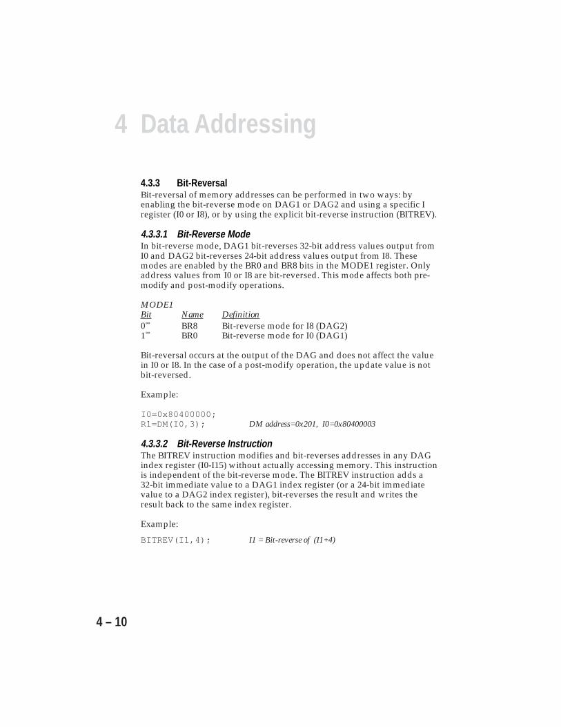
4 Data Addressing
4 – 10
4.3.3 Bit-ReversalBit-reversal of memory addresses can be performed in two ways: byenabling the bit-reverse mode on DAG1 or DAG2 and using a specific Iregister (I0 or I8), or by using the explicit bit-reverse instruction (BITREV).
4.3.3.1 Bit-Reverse ModeIn bit-reverse mode, DAG1 bit-reverses 32-bit address values output fromI0 and DAG2 bit-reverses 24-bit address values output from I8. Thesemodes are enabled by the BR0 and BR8 bits in the MODE1 register. Onlyaddress values from I0 or I8 are bit-reversed. This mode affects both pre-modify and post-modify operations.
MODE1Bit Name Definition0 BR8 Bit-reverse mode for I8 (DAG2)1 BR0 Bit-reverse mode for I0 (DAG1)
Bit-reversal occurs at the output of the DAG and does not affect the valuein I0 or I8. In the case of a post-modify operation, the update value is notbit-reversed.
Example:
I0=0x80400000;R1=DM(I0,3); DM address=0x201, I0=0x80400003
4.3.3.2 Bit-Reverse InstructionThe BITREV instruction modifies and bit-reverses addresses in any DAGindex register (I0-I15) without actually accessing memory. This instructionis independent of the bit-reverse mode. The BITREV instruction adds a32-bit immediate value to a DAG1 index register (or a 24-bit immediatevalue to a DAG2 index register), bit-reverses the result and writes theresult back to the same index register.
Example:
BITREV(I1,4); I1 = Bit-reverse of (I1+4)
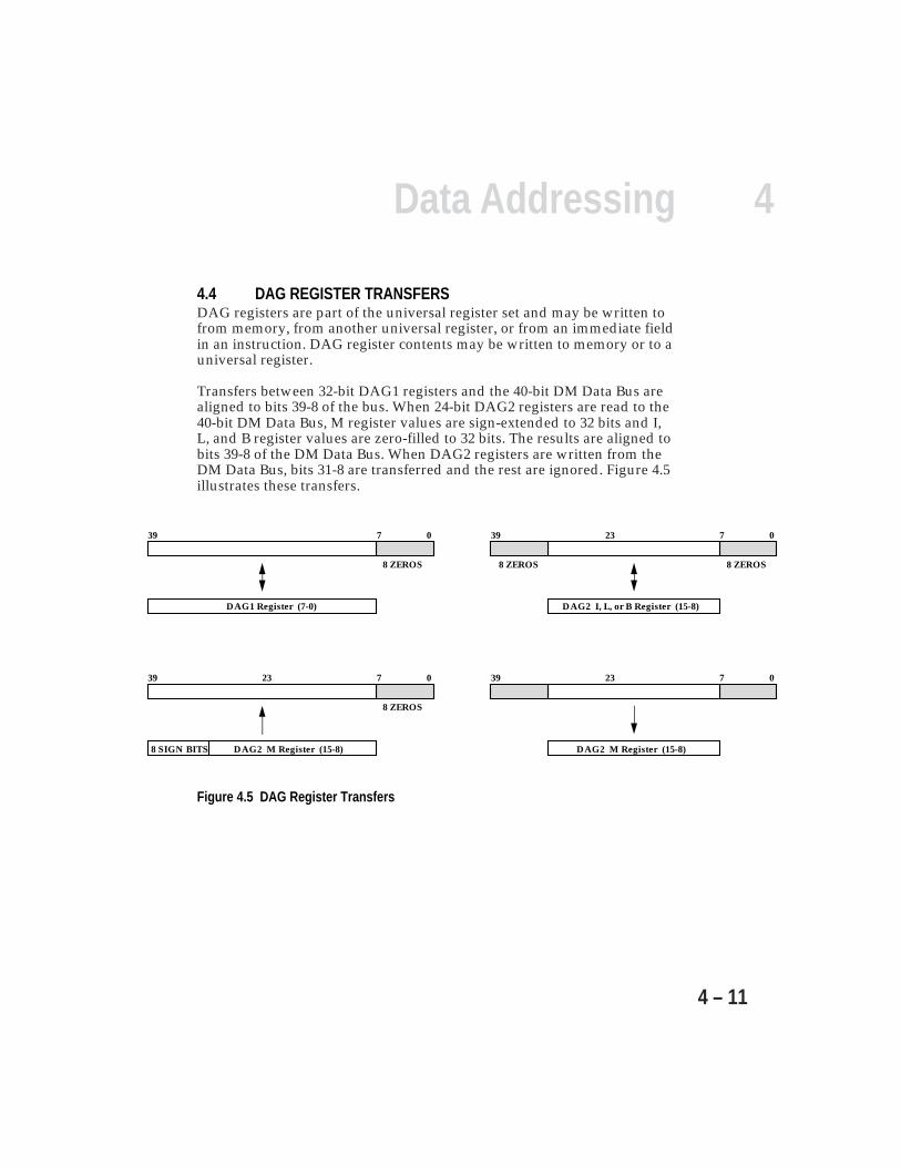
4Data Addressing
4 – 11
4.4 DAG REGISTER TRANSFERSDAG registers are part of the universal register set and may be written tofrom memory, from another universal register, or from an immediate fieldin an instruction. DAG register contents may be written to memory or to auniversal register.
Transfers between 32-bit DAG1 registers and the 40-bit DM Data Bus arealigned to bits 39-8 of the bus. When 24-bit DAG2 registers are read to the40-bit DM Data Bus, M register values are sign-extended to 32 bits and I,L, and B register values are zero-filled to 32 bits. The results are aligned tobits 39-8 of the DM Data Bus. When DAG2 registers are written from theDM Data Bus, bits 31-8 are transferred and the rest are ignored. Figure 4.5illustrates these transfers.
0739
DAG1 Register (7-0)
0739
8 ZEROS
DAG2 I, L, or B Register (15-8)
23
8 ZEROS
0739
8 ZEROS
DAG2 M Register (15-8)
23
8 SIGN BITS
0739
DAG2 M Register (15-8)
23
8 ZEROS
Figure 4.5 DAG Register Transfers
4 Data Addressing
4 – 12
4.4.1 DAG Register Transfer RestrictionsFor certain instruction sequences involving transfers to and from DAGregisters, an extra (NOP) cycle is automatically inserted by the processor (1).Certain other sequences cause incorrect results and are not allowed by theADSP-21000 Family assembler (2).
1.) When an instruction that loads a DAG register is followed by aninstruction that uses any register in the same DAG for data addressing,modify instructions, or indirect jumps, the ADSP-2106x inserts an extra(NOP) cycle between the two instructions. This happens because the samebus is needed by both operations in the same cycle, therefore the secondoperation must be delayed.
Example:
L2=8;DM(I0,M1)=R1;
Because L2 is in the same DAG as I0 (and M1), an extra cycle is inserted afterthe write to L2.
2.) The following types of instructions can execute on the processor, butcause incorrect results; these instructions are disallowed by the ADSP-21000Family assembler:
• An instruction that stores a DAG register in memory using indirectaddressing from the same DAG, with or without update of the indexregister. The instruction writes the wrong data to memory or updates thewrong index register.
Examples:
DM(M2,I1)=I0; or DM(I1,M2)=I0;
• An instruction that loads a DAG register from memory using indirectaddressing from the same DAG, with update of the index register. Theinstruction will either load the DAG register or update the index register,but not both.
Example:
L2=DM(I1,M0);
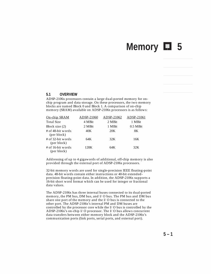
5
5 – 1
Memory
5.1 OVERVIEWADSP-2106x processors contain a large dual-ported memory for on-chip program and data storage. On these processors, the two memoryblocks are named Block 0 and Block 1. A comparison of on-chipmemory (SRAM) available on ADSP-2106x processors is as follows:
On-chip SRAM ADSP-21060 ADSP-21062 ADSP-21061Total Size 4 MBit 2 MBit 1 MBitBlock size (2) 2 MBit 1 MBit 0.5 MBit# of 48-bit words 40K 20K 8K (per block)# of 32-bit words 64K 32K 16K (per block)# of 16-bit words 128K 64K 32K (per block)
Addressing of up to 4 gigawords of additional, off-chip memory is alsoprovided through the external port of ADSP-2106x processors.
32-bit memory words are used for single-precision IEEE floating-pointdata. 48-bit words contain either instructions or 40-bit extended-precision floating-point data. In addition, the ADSP-2106x supports a16-bit short word format which can be used for integer or fractionaldata values.
The ADSP-2106x has three internal buses connected to its dual-portedmemory, the PM bus, DM bus, and I/O bus. The PM bus and DM busshare one port of the memory and the I/O bus is connected to theother port. The ADSP-2106x’s internal PM and DM buses arecontrolled by the processor core while the I/O bus is controlled by theADSP-2106x’s on-chip I/O processor. The I/O bus allows concurrentdata transfers between either memory block and the ADSP-2106x’scommunication ports (link ports, serial ports, and external port).
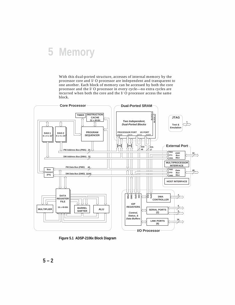
5 Memory
5 – 2
With this dual-ported structure, accesses of internal memory by theprocessor core and I/O processor are independent and transparent toone another. Each block of memory can be accessed by both the coreprocessor and the I/O processor in every cycle—no extra cycles areincurred when both the core and the I/O processor access the sameblock.
AAAAAAAAAAAAAAAAAAAAAAAAAAAAAAAAAAA
PM Address Bus (PMA) 24
DM Address Bus (DMA) 32
PM Data Bus (PMD)
DM Data Bus (DMD)
AAAAAA AAAAAA
AAAAAA
AAAAAAAAAAAAAAAAAAAAAAAAAAAAAAAAAAA
PROCESSOR PORT I/O PORT
SERIAL PORTS (2)
LINK PORTS (6)
INSTRUCTIONCACHE
32 x 48-Bit
DAG 28 x 4 x 24
DAG 18 x 4 x 32
TIMER
DMA CONTROLLER
Addr Bus Mux
32
48
AAAAAAAAAAAAAAAAAAAAAAAA
IOPREGISTERS
Control,Status, &
Data Buffers
6
6
36
4AAAAAAAAAAAAAAAAAAAAAAAAAAAAAAA
AAAAAAAAAAAAAAAAAAAAAAA
AA
ADDR DATA ADDR DATA
AA
7
A
A
JTAG
Bus Connect
(PX)
MULTIPLIER BARREL SHIFTER
ALU
AAAAAAAA
AAAAAAA
DATAREGISTER
FILE
16 x 40-Bit
AAAAAACore Processor AAAAADual-Ported SRAM
Two Independent,Dual-Ported Blocks
BL
OC
K 0
BL
OC
K 1
AAAAAAAAAAExternal Port
HOST INTERFACE
Test &Emulation
PROGRAMSEQUENCER
MULTIPROCESSORINTERFACE
48
IOD48
IOA17
AAAAAAAAA
IOD
EP
D
DM
D
PM
D
EP
A
IOA
AAAAAI/O Processor
AAAAAAA32/40
PMA
EPA
DMA
PMD
EPD
DMD
Data Bus Mux
AAAAAAAAAAAAA
Figure 5.1 ADSP-2106x Block Diagram
5Memory
5 – 3
Both the core processor and I/O processor have access to the external bus(DATA47-0 , ADDR31-0), via the ADSP-2106x’s external port. The externalport provides access to off-chip memory and peripherals; it can also accessthe internal memory of other ADSP-2106xs connected in a multiprocessingsystem. This busing scheme allows the ADSP-2106x to have a singleunified address space in which both code and data is stored.
External memory can be either 16, 32, or 48 bits wide; the ADSP-2106x’sDMA controller automatically packs external data into the appropriateword width, either 48-bit instructions or 32-bit data.
Note that the ADSP-2106x’s internal memory is divided into two blocks,called Block 0 and Block 1, while the external memory space is dividedinto four banks.
5.1.1 Dual Data AccessesThe ADSP-2100 and ADSP-21000 Family DSPs traditionally definememory as either program memory, for instructions, or as data memory,for data storage. The processors’ modified Harvard architecture, however,allows data storage within program memory. The ADSP-2106x retains theADSP-21000 Family’s separate on-chip buses for program memory anddata memory, but does not pre-define the two on-chip memory blocks aseither PM or DM. This allows the memory to be freely configured to storedifferent combinations of code and data.
The independent PM and DM buses allow the ADSP-2106x’s processorcore to simultaneously access instructions and data from both memoryblocks. If the core tries to access two words from the same memory block(over the same bus) for a single instruction, however, an extra cycle isneeded. Instructions are fetched over the PM bus or from the instructioncache. Data can be accessed over both the DM bus (using DAG1) and thePM bus (using DAG2). Figure 5.1 shows the memory bus connections onthe ADSP-2106x.
The ADSP-2106x’s two memory blocks can be configured to store differentcombinations of 48-bit instruction words and 32-bit data words.Maximum efficiency (i.e. single-cycle execution of dual-data-accessinstructions), though, is achieved when one block contains a mix ofinstructions and PM bus data while the other block contains DM bus dataonly.

5 Memory
5 – 4
This means that for an instruction requiring two data accesses, thePM bus (and DAG2) is used to access data from the mixed block, theDM bus (and DAG1) is used to access data from the data-only block,and the instruction to be fetched must be available from the cache. Anotherway to partition the data is to store one operand in external memoryand the other in either block of internal memory.
In typical DSP applications such as digital filters and FFTs, two dataoperands must be accessed for some instructions. In a digital filter, forexample, the filter coefficients can be stored in 32-bit words in thesame memory block that contains the 48-bit instructions, while 32-bitdata samples are stored in the other block. This provides single-cycleexecution of dual-data-access instructions, with the filter coefficientsbeing accessed by DAG2 over the PM bus and the instruction availablefrom the cache.
In summary, to assure single-cycle, parallel accesses of two on-chipmemory locations, the following conditions must be met:
• The two addresses must be located in different memory blocks(i.e. one in Block 0, one in Block 1).
• One address must be generated by DAG1 and the other by DAG2.• The DAG1 address must not point to the same memory block that
instructions are being fetched from.• The instruction should be of the form:
compute, Rx=DM(I0 -I7,M0 -M7), Ry=PM(I8 -I15,M8 -M15);
(Note that reads and writes may be intermixed.)
Remember that a cache miss will occur if the fetched instruction is notvalid during any DAG2 transfer.
5.1.2 Instruction Cache & PM Bus Data AccessesNormally the ADSP-2106x fetches instructions over the 48-bit PM Databus. When, however, the processor executes a dual-data-accessinstruction that requires data to be read or written over the PM bus,there is a conflict for use of the PM Data bus. The ADSP-2106x’son-chip instruction cache can resolve this conflict by providing theinstruction (once it is stored in the cache, the first time it is executed).
5Memory
5 – 5
By providing the instruction, the cache lets the core processor accessdata over the PM bus—the core processor fetches the instruction fromthe cache instead of from memory so that the processor cansimultaneously transfer data over the PM bus. Only the instructionswhose fetches conflict with PM bus data accesses are cached.
The instruction cache allows data to be accessed over the PM bus,without any extra cycles, whenever the instruction to be fetched isalready cached (i.e. within a loop). An extra cycle will always occur inthe event of a cache miss, even if the instruction and data are indifferent memory blocks but use the same bus.
5.1.3 On-Chip Memory Buses & Address GenerationThe ADSP-2106x has three internal buses connected to its dual-portedmemory, the PM bus, DM bus, and I/O bus. The PM bus and DM busshare one port of the memory and the I/O bus is connected to theother port.
The ADSP-2106x’s program sequencer and data address generators(DAGs) supply memory addresses. The program sequencer supplies24-bit PM bus addresses for instruction fetches. The DAGs supplyaddresses for data reads and writes. (See Figure 5.1.)
The two data address generators allow indirect addressing of data.DAG1 supplies 32-bit addresses over the DM bus. DAG2 supplies24-bit addresses for PM bus data accesses. The two DAGs can generatesimultaneous addresses—over the PM bus and DM bus—for dualoperand read/writes, if the instruction to be fetched is available fromthe cache.
The 48-bit PM Data bus is used to transfer instructions (and data), andthe 40-bit DM Data bus is used to transfer data. The PM Data bus is48 bits wide to accommodate the 48-bit instruction width. When thisbus is used to transfer 32-bit floating-point or 32-bit fixed-point data,the data is aligned to the upper 32 bits of the bus.
The 40-bit DM Data bus provides a path for the contents of any registerin the processor to be transferred to any other register or to anyexternal memory location in a single cycle. Data addresses come fromone of two sources: an absolute value specified in the instruction(direct addressing), or the output of a data address generator(indirect addressing). 32-bit fixed-point and 32-bit single-precisionfloating-point data is also aligned to the upper 32 bits of the DM Databus.

5 Memory
5 – 6
The PX bus connect registers permit data to be passed between the48-bit PM Data bus and the 40-bit DM Data bus or between the 40-bitregister file and the PM Data bus. These registers contain hardware tohandle the 8-bit width difference.
The three memory buses—PM, DM, and I/O—are multiplexed at theprocessor’s external port to create a single off-chip data bus (DATA47-0)and address bus (ADDR31-0).
5.1.4 Bus Exchange (PX Registers)The PX register provides an internal bus exchange path for transferringdata between the 48-bit PM Data Bus and the 40-bit DM Data Bus. The48-bit PX register consists of PX1 and PX2. PX1 is 16 bits wide and PX2 is32 bits wide. PX1 and PX2 can be used separately in instructions and canalso be treated as the combined PX register. The alignment of PX1 andPX2 within PX is shown below in Figure 5.2.
Figure 5.2 PX Register
Either PX1, PX2, or the combined PX register can be used in universalregister-to-register transfers or in memory-to-register (and register-to-memory) transfers. These transfers may take place over the PM Data Busor DM Data Bus. The PX register(s) can be read from or written to thePM Data Bus, the DM Data Bus, or the register file.
Data is aligned in PX register transfers as shown in Figure 5.3. Whendata is transferred between PX2 and the PM Data Bus, the upper 32 bitsof the PM Data Bus are used. On transfers from PX2, the 16 LSBs of thePM Data Bus are filled with zeros. When data is transferred betweenPX1 and the PM Data Bus, the middle 16 bits of the PM Data Bus areused. On transfers from PX1, bits 15-0 and bits 47-32 are filled withzeros.
PX2 PX1
PX Register
01547

5Memory
5 – 7
01547
16 ZEROS
0739
8 ZEROS
PX2PX2
01547
16 ZEROS
0739
8 ZEROS
PX1PX1
16 ZEROS
31
16 ZEROS
23
01547
PX2 PX1
PX Register
PM Data Bus Transfers DM Data Bus or Register File Transfers
0
747
PX Register
0
39Register File
0
47
PX Register
39To Internal Memory
07
8 ZEROS
0
47
PX Register
47To External Memory
0
Figure 5.3 PX Register Transfers
5 Memory
5 – 8
When the combined PX register is used for PM Data Bus transfers, theentire 48 bits can be read from or written to program memory.PX2 contains the 32 MSBs of the 48-bit word while PX1 contains the16 LSBs. (PM Bus data is left-justified in the 48-bit word.)
To write a 48-bit word to the memory location named Port1 over thePM Data Bus, for example, the following instructions could be used:
R0=0x9A00; /* load R0 with 16 LSBs */R1=0x12345678; /* load R1 with 32 MSBs */PX1=R0;PX2=R1;PM(Port1)=PX; /* write 16 LSBs on PM bus 15-0 */ /* and 32 MSBs on PM bus 47-16 */
When data is transferred between PX2 and the DM Data Bus or theregister file, the upper 32 bits of the DM Data Bus (and register file) areused. On transfers from PX2, the eight LSBs are filled with zeros. (SeeFigure 5.3.) When data is transferred between PX1 and the DM DataBus or the register file, bits 23-8 of the DM Data Bus (and register file)are used. On transfers from PX1, bits 7-0 and bits 39-24 are filled withzeros.
When the combined PX register is used for DM Data Bus transfers, theupper 40 bits of PX are read or written. For transfers to or from internalmemory, the lower 8 bits are filled with zeroes. For transfers to or fromexternal memory, the entire 48 bits are transferred.
5.1.5 Memory Block Accesses & ConflictsAny of the ADSP-2106x’s three internal buses, PM, DM, and I/O, mayneed to access one of the memory blocks at any given time. Each blockof dual-ported memory can be accessed by both the ADSP-2106x’s coreprocessor (over either the PM or DM bus) and by the I/O processor(over the I/O bus) in every cycle—no extra cycles are incurred whenboth the core and I/O processor access the same block.
A conflict occurs, however, when two core accesses to a single blockare attempted in the same cycle, for example over both the PM bus (bythe program sequencer or DAG2) and DM bus (by DAG1). When thishappens, an extra cycle is incurred—the DM bus access completes firstand the PM bus access completes in the following (extra) cycle.

5Memory
5 – 9
5.2 ADSP-2106x MEMORY MAPThe ADSP-2106x memory map, shown in Figure 5.5, is divided into threesections: internal memory space, multiprocessor memory space, andexternal memory space. Internal memory space consists of theADSP-2106x’s on-chip memory and resources. Multiprocessor memoryspace corresponds to the on-chip memory and resources of otherADSP-2106x’s in a multiprocessor system. External memory spacecorresponds to off-chip memory and memory-mapped I/O devices.
The address boundaries of each memory space are:
Internal memory 0x0000 0000 to 0x0007 FFFFMultiprocessor memory 0x0008 0000 to 0x003F FFFFExternal memory 0x0040 0000 to 0xFFFF FFFF
Addresses generated by the ADSP-2106x for DM bus and PM bus accessesare shown below in Figure 5.4. DM bus addresses are generated by DAG1,and PM bus addresses are generated either by the ADSP-2106x’s programsequencer (for instructions) or by DAG2 (for data).
16 0182131
SME
16 01821
SME
(generated by DAG1)
(generated by Program Sequencer or DAG2)
23
Note: Off-chip PM bus addresses are MSB-extended with zerosto create 32-bit external bus addresses (ADDR31-0).
DM Bus Addresses
PM Bus Addresses
Figure 5.4 Memory Addresses (E = external, M = Multiprocessor, S = Internal)
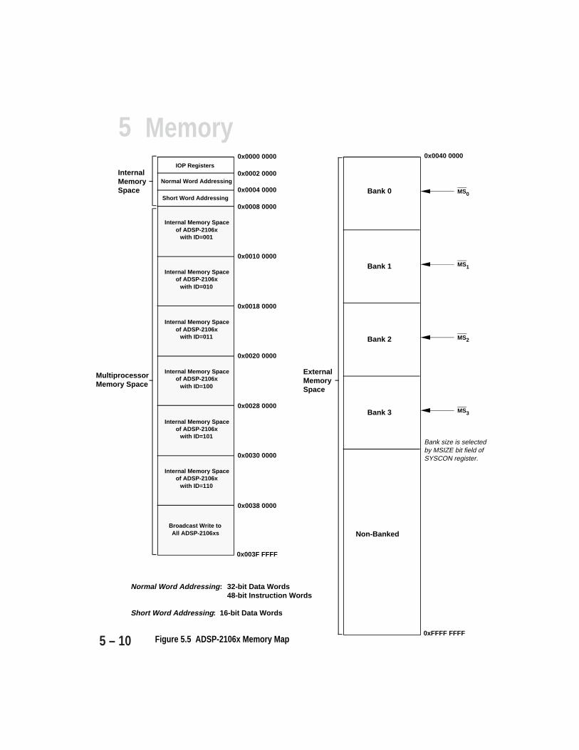
5 Memory
5 – 10 Figure 5.5 ADSP-2106x Memory Map
Normal Word Addressing: 32-bit Data Words 48-bit Instruction Words
Short Word Addressing: 16-bit Data Words
IOP Registers
Normal Word Addressing
Short Word Addressing
0x0000 0000
0x0002 0000
0x0004 0000
0x0008 0000
0x0010 0000
0x0018 0000
0x0020 0000
0x0028 0000
0x0030 0000
0x0038 0000
Broadcast Write toAll ADSP-2106xs
InternalMemorySpace
MultiprocessorMemory Space
MS0Bank 0
0x0040 0000
0xFFFF FFFF
ExternalMemorySpace
0x003F FFFF
Bank 1
Bank 2
Bank 3
Non-Banked
Bank size is selected by MSIZE bit field of SYSCON register.
Internal Memory Spaceof ADSP-2106x
with ID=001
Internal Memory Spaceof ADSP-2106x
with ID=010
Internal Memory Spaceof ADSP-2106x
with ID=011
Internal Memory Spaceof ADSP-2106x
with ID=100
Internal Memory Spaceof ADSP-2106x
with ID=101
Internal Memory Spaceof ADSP-2106x
with ID=110
MS1
MS2
MS3
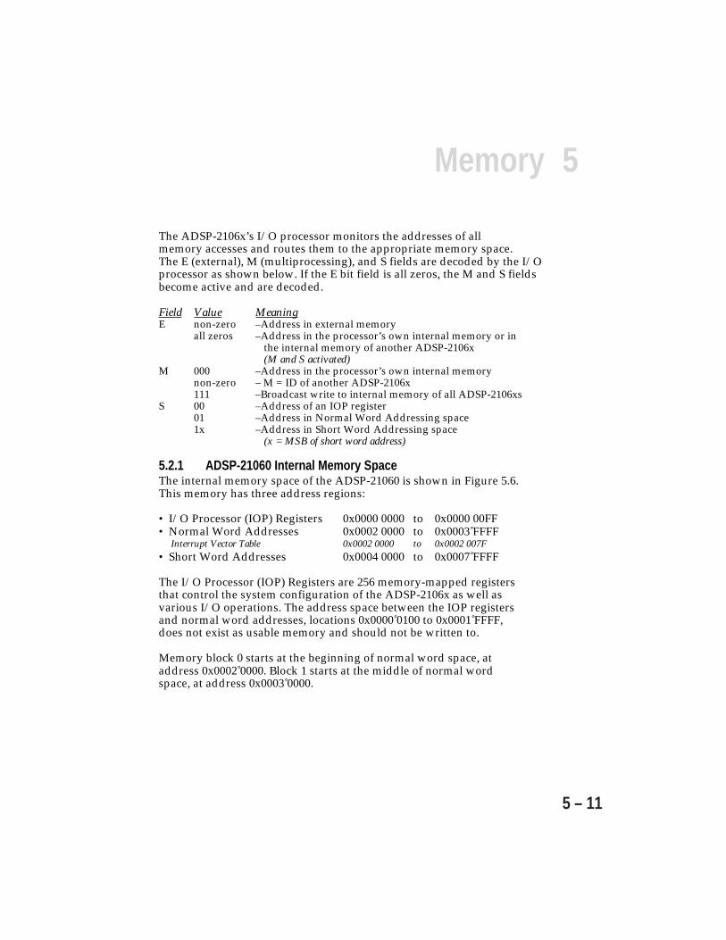
5Memory
5 – 11
The ADSP-2106x’s I/O processor monitors the addresses of allmemory accesses and routes them to the appropriate memory space.The E (external), M (multiprocessing), and S fields are decoded by the I/Oprocessor as shown below. If the E bit field is all zeros, the M and S fieldsbecome active and are decoded.
Field Value MeaningE non-zero –Address in external memory
all zeros –Address in the processor’s own internal memory or inthe internal memory of another ADSP-2106x(M and S activated)
M 000 –Address in the processor’s own internal memorynon-zero – M = ID of another ADSP-2106x111 –Broadcast write to internal memory of all ADSP-2106xs
S 00 –Address of an IOP register01 –Address in Normal Word Addressing space1x –Address in Short Word Addressing space
(x = MSB of short word address)
5.2.1 ADSP-21060 Internal Memory SpaceThe internal memory space of the ADSP-21060 is shown in Figure 5.6.This memory has three address regions:
• I/O Processor (IOP) Registers 0x0000 0000 to 0x0000 00FF• Normal Word Addresses 0x0002 0000 to 0x0003 FFFF Interrupt Vector Table 0x0002 0000 to 0x0002 007F• Short Word Addresses 0x0004 0000 to 0x0007 FFFF
The I/O Processor (IOP) Registers are 256 memory-mapped registersthat control the system configuration of the ADSP-2106x as well asvarious I/O operations. The address space between the IOP registersand normal word addresses, locations 0x0000 0100 to 0x0001 FFFF,does not exist as usable memory and should not be written to.
Memory block 0 starts at the beginning of normal word space, ataddress 0x0002 0000. Block 1 starts at the middle of normal wordspace, at address 0x0003 0000.
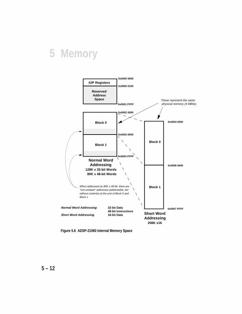
5 Memory
5 – 12
Figure 5.6 ADSP-21060 Internal Memory Space
Normal Word Addressing: 32-bit Data48-bit Instructions
Short Word Addressing: 16-bit Data
0x0006 0000
0x0007 FFFF
Block 1
Block 0
Normal Word Addressing
128K x 32-bit Words 80K x 48-bit Words
0x0002 0000
0x0003 FFFF
Short Word Addressing
256K x16
0x0004 0000
Block 1
Block 0
0x0003 0000
These represent the same physical memory (4 MBits)
When addressed as 80K x 48-bit, there are "non-existant" addresses (addressible, but without contents) at the end of Block 0 and Block 1
0x0000 0000
0x0001 FFFF
IOP Registers0x0000 0100
ReservedAddressSpace
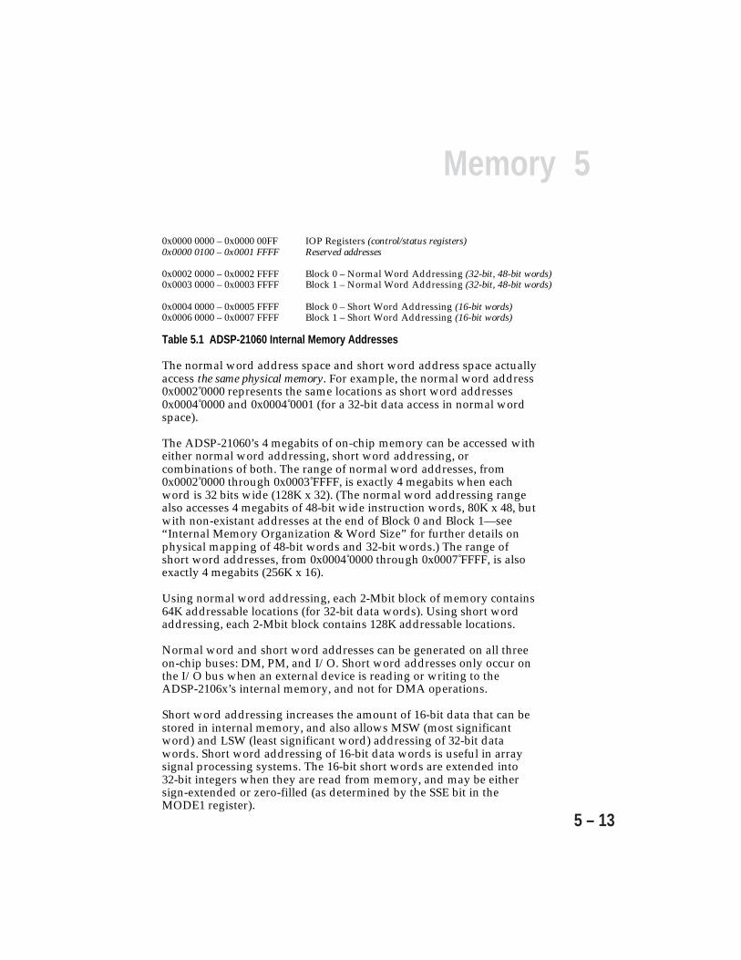
5Memory
5 – 13
0x0000 0000 – 0x0000 00FF IOP Registers (control/status registers)0x0000 0100 – 0x0001 FFFF Reserved addresses
0x0002 0000 – 0x0002 FFFF Block 0 – Normal Word Addressing (32-bit, 48-bit words)0x0003 0000 – 0x0003 FFFF Block 1 – Normal Word Addressing (32-bit, 48-bit words)
0x0004 0000 – 0x0005 FFFF Block 0 – Short Word Addressing (16-bit words)0x0006 0000 – 0x0007 FFFF Block 1 – Short Word Addressing (16-bit words)
Table 5.1 ADSP-21060 Internal Memory Addresses
The normal word address space and short word address space actuallyaccess the same physical memory. For example, the normal word address0x0002 0000 represents the same locations as short word addresses0x0004 0000 and 0x0004 0001 (for a 32-bit data access in normal wordspace).
The ADSP-21060’s 4 megabits of on-chip memory can be accessed witheither normal word addressing, short word addressing, orcombinations of both. The range of normal word addresses, from0x0002 0000 through 0x0003 FFFF, is exactly 4 megabits when eachword is 32 bits wide (128K x 32). (The normal word addressing rangealso accesses 4 megabits of 48-bit wide instruction words, 80K x 48, butwith non-existant addresses at the end of Block 0 and Block 1—see“Internal Memory Organization & Word Size” for further details onphysical mapping of 48-bit words and 32-bit words.) The range ofshort word addresses, from 0x0004 0000 through 0x0007 FFFF, is alsoexactly 4 megabits (256K x 16).
Using normal word addressing, each 2-Mbit block of memory contains64K addressable locations (for 32-bit data words). Using short wordaddressing, each 2-Mbit block contains 128K addressable locations.
Normal word and short word addresses can be generated on all threeon-chip buses: DM, PM, and I/O. Short word addresses only occur onthe I/O bus when an external device is reading or writing to theADSP-2106x’s internal memory, and not for DMA operations.
Short word addressing increases the amount of 16-bit data that can bestored in internal memory, and also allows MSW (most significantword) and LSW (least significant word) addressing of 32-bit datawords. Short word addressing of 16-bit data words is useful in arraysignal processing systems. The 16-bit short words are extended into32-bit integers when they are read from memory, and may be eithersign-extended or zero-filled (as determined by the SSE bit in theMODE1 register).
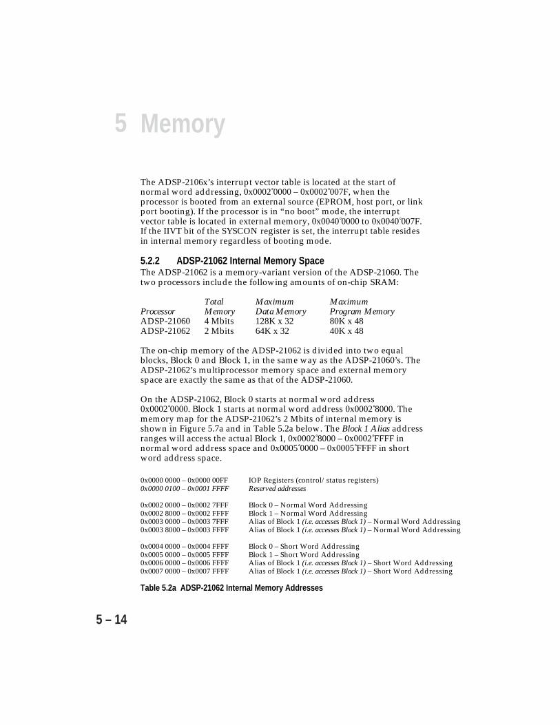
5 Memory
5 – 14
The ADSP-2106x’s interrupt vector table is located at the start ofnormal word addressing, 0x0002 0000 – 0x0002 007F, when theprocessor is booted from an external source (EPROM, host port, or linkport booting). If the processor is in “no boot” mode, the interruptvector table is located in external memory, 0x0040 0000 to 0x0040 007F.If the IIVT bit of the SYSCON register is set, the interrupt table residesin internal memory regardless of booting mode.
5.2.2 ADSP-21062 Internal Memory SpaceThe ADSP-21062 is a memory-variant version of the ADSP-21060. Thetwo processors include the following amounts of on-chip SRAM:
Total Maximum MaximumProcessor Memory Data Memory Program MemoryADSP-21060 4 Mbits 128K x 32 80K x 48ADSP-21062 2 Mbits 64K x 32 40K x 48
The on-chip memory of the ADSP-21062 is divided into two equalblocks, Block 0 and Block 1, in the same way as the ADSP-21060’s. TheADSP-21062’s multiprocessor memory space and external memoryspace are exactly the same as that of the ADSP-21060.
On the ADSP-21062, Block 0 starts at normal word address0x0002 0000. Block 1 starts at normal word address 0x0002 8000. Thememory map for the ADSP-21062’s 2 Mbits of internal memory isshown in Figure 5.7a and in Table 5.2a below. The Block 1 Alias addressranges will access the actual Block 1, 0x0002 8000 – 0x0002 FFFF innormal word address space and 0x0005 0000 – 0x0005 FFFF in shortword address space.
0x0000 0000 – 0x0000 00FF IOP Registers (control/status registers)0x0000 0100 – 0x0001 FFFF Reserved addresses
0x0002 0000 – 0x0002 7FFF Block 0 – Normal Word Addressing0x0002 8000 – 0x0002 FFFF Block 1 – Normal Word Addressing0x0003 0000 – 0x0003 7FFF Alias of Block 1 (i.e. accesses Block 1) – Normal Word Addressing0x0003 8000 – 0x0003 FFFF Alias of Block 1 (i.e. accesses Block 1) – Normal Word Addressing
0x0004 0000 – 0x0004 FFFF Block 0 – Short Word Addressing0x0005 0000 – 0x0005 FFFF Block 1 – Short Word Addressing0x0006 0000 – 0x0006 FFFF Alias of Block 1 (i.e. accesses Block 1) – Short Word Addressing0x0007 0000 – 0x0007 FFFF Alias of Block 1 (i.e. accesses Block 1) – Short Word Addressing
Table 5.2a ADSP-21062 Internal Memory Addresses
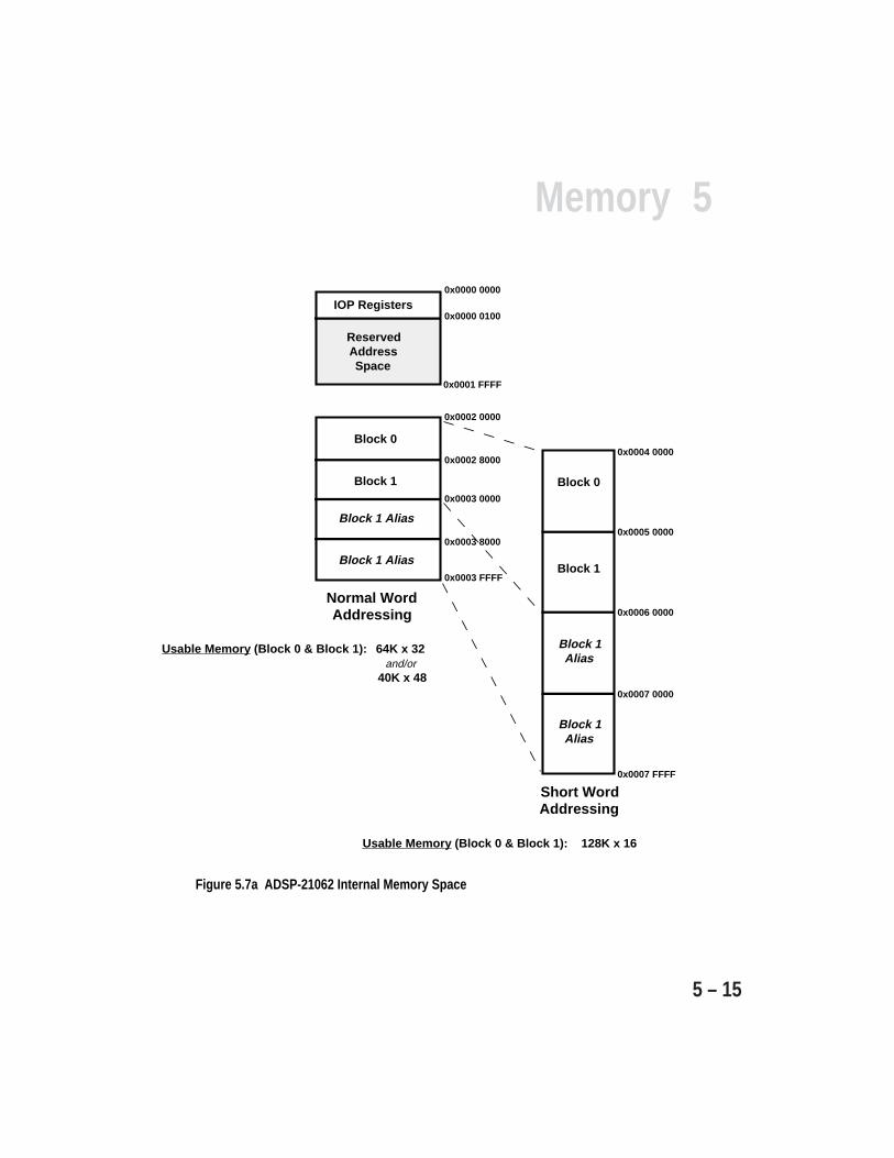
5Memory
5 – 15
Figure 5.7a ADSP-21062 Internal Memory Space
Normal Word Addressing
Usable Memory (Block 0 & Block 1): 64K x 32and/or
40K x 48
Short Word Addressing
128K x 16
0x0006 0000
Block 1
Block 0
0x0002 0000
0x0004 0000
Block 1
Block 00x0003 0000
Block 1 Alias
Block 1 Alias
0x0002 8000
0x0003 8000
Block 1Alias
Block 1Alias
0x0005 0000
0x0007 0000
0x0007 FFFF
0x0003 FFFF
Usable Memory (Block 0 & Block 1):
0x0000 0000
0x0001 FFFF
IOP Registers0x0000 0100
ReservedAddressSpace
5 Memory
5 – 16
5.2.3 ADSP-21061 Internal Memory SpaceThe ADSP-21061 is a memory-variant version of the ADSP-21060. Thetwo processors include the following amounts of on-chip SRAM:
Total Maximum MaximumProcessor Memory Data Memory Program MemoryADSP-21060 4 Mbits 128K x 32 80K x 48ADSP-21062 1 Mbits 32K x 32 16K x 48
The on-chip memory of the ADSP-21061 is divided into two equalblocks, Block 0 and Block 1, in the same way as the ADSP-21060’s. TheADSP-21061’s multiprocessor memory space and external memoryspace are exactly the same as that of the ADSP-21060.
On the ADSP-21061, Block 0 starts at normal word address0x0002 0000. Block 1 starts at normal word address 0x0002 4000. Thememory map for the ADSP-21061’s 1 Mbit of internal memory isshown in Figure 5.7b and in Table 5.2b below. The Block 1 Alias addressranges will access the actual Block 1, 0x0002 4000 – 0x0002 7FFF innormal word address space and 0x0004 8000 – 0x0004 FFFF in shortword address space.
0x0000 0000 – 0x0000 00FF IOP Registers (control/status registers)0x0000 0100 – 0x0001 FFFF Reserved addresses
0x0002 0000 – 0x0002 3FFF Block 0 – Normal Word Addressing0x0002 4000 – 0x0002 7FFF Block 1 – Normal Word Addressing0x0002 8000 – 0x0002 BFFF Alias of Block 1 (i.e. accesses Block 1) – Normal Word Addressing0x0002 C000 – 0x0002 FFFF Alias of Block 1 (i.e. accesses Block 1) – Normal Word Addressing0x0003 0000 – 0x0003 3FFF Alias of Block 1 (i.e. accesses Block 1) – Normal Word Addressing0x0003 4000 – 0x0003 7FFF Alias of Block 1 (i.e. accesses Block 1) – Normal Word Addressing0x0003 8000 – 0x0003 BFFF Alias of Block 1 (i.e. accesses Block 1) – Normal Word Addressing0x0003 C000 – 0x0003 FFFF Alias of Block 1 (i.e. accesses Block 1) – Normal Word Addressing
0x0004 0000 – 0x0004 7FFF Block 0 – Short Word Addressing0x0004 8000 – 0x0004 FFFF Block 1 – Short Word Addressing0x0005 0000 – 0x0005 7FFF Alias of Block 1 (i.e. accesses Block 1) – Short Word Addressing0x0005 8000 – 0x0005 FFFF Alias of Block 1 (i.e. accesses Block 1) – Short Word Addressing0x0006 0000 – 0x0006 7FFF Alias of Block 1 (i.e. accesses Block 1) – Short Word Addressing0x0006 8000 – 0x0006 FFFF Alias of Block 1 (i.e. accesses Block 1) – Short Word Addressing0x0007 0000 – 0x0007 7FFF Alias of Block 1 (i.e. accesses Block 1) – Short Word Addressing0x0007 8000 – 0x0007 FFFF Alias of Block 1 (i.e. accesses Block 1) – Short Word Addressing
Table 5.2b ADSP-21061 Internal Memory Addresses
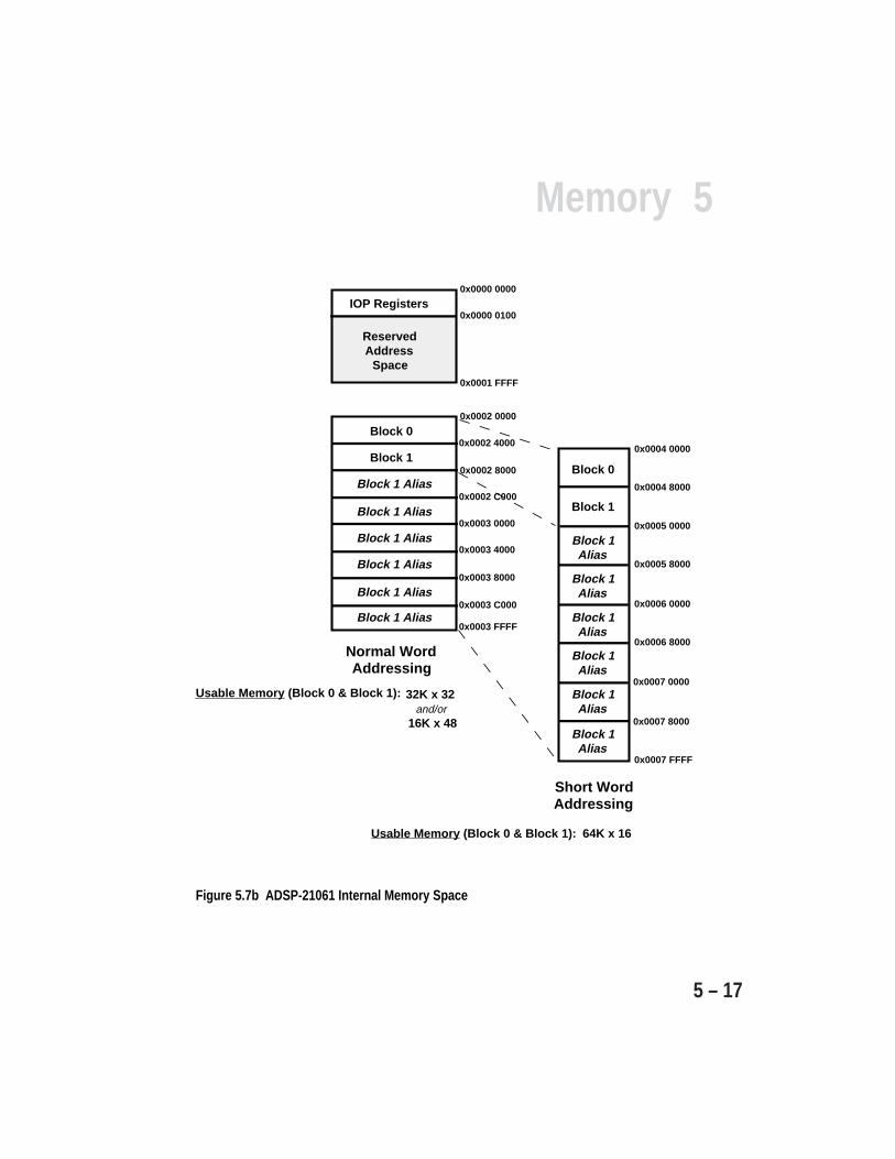
5Memory
5 – 17
Figure 5.7b ADSP-21061 Internal Memory Space
Normal Word Addressing
Usable Memory (Block 0 & Block 1): 32K x 32and/or
16K x 48
Short Word Addressing
64K x 16
0x0006 0000
Block 1
Block 00x0002 0000
0x0004 0000
Block 1
Block 0
0x0002 C000Block 1 Alias
Block 1 Alias
0x0002 8000
0x0003 4000Block 1Alias
Block 1Alias
0x0005 0000
0x0007 0000
0x0007 FFFF
0x0003 8000
Usable Memory (Block 0 & Block 1):
0x0000 0000
0x0001 FFFF
IOP Registers0x0000 0100
ReservedAddress
Space
Block 1 Alias
Block 1 Alias
Block 1 Alias
Block 1 Alias
0x0002 4000
0x0003 0000
0x0003 C000
0x0003 FFFFBlock 1Alias
Block 1Alias
Block 1Alias
Block 1Alias
0x0004 8000
0x0005 8000
0x0006 8000
0x0007 8000
5 Memory
5 – 18
5.2.4 Porting Code from ADSP-21060 to ADSP-21062 or ADSP-21061To ease porting code between ADSP-2106x processor, a system foraliasing memory Block 1 eliminates the need to re-arrange (some) codeplacement. For example, memory Block 0 on the ADSP-21062 starts atthe beginning of internal memory, normal word address 0x0002 0000.Block 1 on the ADSP-21062 starts at the end of Block 0, withcontiguous addresses. The remaining addresses in internal memoryare divided into blocks, which alias into Block 1. This aliasing allowsany code or data stored in Block 1 on the ADSP-21060 to retain thesame addresses on the ADSP-21062—these addresses will alias into theactual Block 1 of each processor.
A similar aliasing structure is built into the ADSP-21061. For moreinformation on aliasing, see the memory maps for the ADSP-21061 andADSP-21062 processors.
5.2.5 Multiprocessor Memory SpaceMultiprocessor memory space maps to the internal memory of otherADSP-2106xs in a multiprocessor system. This allows eachADSP-2106x to access the internal memory and memory-mapped IOPregisters of the other processors.
As shown in Figure 5.5, when the E field of an address is zero and theM field is non-zero, the address falls within multiprocessor memoryspace. The value of M specifies the processor ID2-0 of the externalADSP-2106x being accessed, and only that processor will respond tothe read/write cycle. If M=111, however, a broadcast write is performedto all processors. All of the processors react to this address as if theirindividual ID2-0 was being used, enabling the write to their internalmemory.
Instead of directly accessing its own internal memory, an ADSP-2106xcan also access its memory through the multiprocessor memory spaceby using its own ID. In this case the processor simply reads or writes toits own internal memory and does not attempt an access on theexternal system bus. (Note that these self-accesses throughmultiprocessor memory space may only be accomplished withcore-processor-generated addresses, not DMA-controller-generatedaddresses.)
If both the E and M fields of an address on the external bus are equal tozero, the address will be ignored unless the processor ID is also zero
5Memory
5 – 19
(M=ID2-0 =000). Addresses with M=ID2-0 =000 are only allowed insingle-processor systems.
If the ADSP-2106x attempts to access an invalid address inmultiprocessor memory space, data written will be ignored and readswill return invalid data.
For additional information about multiprocessor memory accesses, see“Direct Reads & Writes” and “Data Transfers Through The EPBxBuffers” in the Multiprocessing chapter of this manual.
5.2.6 External Memory SpaceExternal memory can be accessed over the ADSP-2106x’s DM bus,PM bus, and EP bus, all via the external port. The processor’s DAG1,program sequencer (and DAG2), and IOP control these respectivebuses.
32-bit addresses are generated by DAG1 and the IOP over the DM addressbus and I/O address bus, allowing addressing of the complete 4-gigawordmemory map. The program sequencer and DAG2 generate 24-bitaddresses over the PM address bus, limiting addressing to the low12 megawords (0x0040 0000 to 0x00FF FFFF).
5.2.7 Memory Space Access RestrictionsThe ADSP-2106x’s three internal buses, PM, DM, and I/O, can be usedto access the processor’s memory map according to the following rules:
• The DM bus can access all memory spaces.• The PM bus can access only Internal Memory Space and the lowest
12 megawords of External Memory Space.• The I/O bus can access all memory spaces except for the memory-
mapped IOP registers (in Internal Memory Space).
Note that in silicon revision 1.0 and earlier pre-modify addressingoperations must not change the memory space of the address; forexample, pre-modification of an address in Internal Memory Spaceshould not generate an address in External Memory Space. The oneexception to this rule is: an indirect JUMP or CALL instruction withpre-modify addressing can jump from internal memory to externalmemory. Silicon revisions 2.x and later do not have this pre-modifylimitation.
5 Memory
5 – 20
5.3 INTERNAL MEMORY ORGANIZATION & WORD SIZEThe ADSP-2106x’s internal SRAM memory accommodates thefollowing word types:
• 48-bit instructions• 32-bit floating-point data• 16-bit short word data
40-bit extended-precision floating-point data values are alsoaccommodated, but are accessed in 48-bit words. The 40 bits are left-justified in the 48-bit word (bits 47-8).
When the ADSP-2106x processor core accesses its internal memory, theword width of the access is determined according to the followingrules:
• Instruction fetches always read 48-bit words• Read/writes using normal word addressing are either 32-bit words or
48-bit words, depending on how the block of memory is configured inthe SYSCON register.
• Read/writes using short word addressing are always 16-bit words• PM bus (DAG 2) read/writes of the PX register are always 48-bit words
(unless they use short word addressing)• DM bus (DAG 1) read/writes of the PX register are always 40-bit words
(unless they use short word addressing)
An ADSP-2106x program should not attempt to access the samephysical location in memory as a 32-bit word and as a 48-bit word. Theinternal SRAM employs a write-back scheme that will cause errors ifthis occurs.
5.3.1 32-Bit Words & 48-Bit WordsEach 2-Mbit block of ADSP-21060 memory is physically organized as16 columns, each 16 bits wide, with a height of 8K. (On theADSP-21062, each 1-Mbit block of memory is similarly organized butwith each column having a height of 4K.) 48-bit instruction wordsrequire three columns of contiguous memory and 32-bit data wordsrequire two contiguous columns.

5Memory
5 – 21
When an address is applied to memory for a read or write, theparticular columns selected depends upon the word width of theaccess. For 48-bit words, the 16-bit columns are selected in groups ofthree. In a memory block consisting entirely of 48-bit instructionwords,
16 columns ÷ 3 columns per group = 5 groups
there are 5 groups to select from and the 16th column is unused. Thus,an ADSP-21060 2-Mbit memory block that consists entirely of 48-bitwords provides
8K × 5 groups = 40K words
of instruction storage. For 32-bit data words, the columns are selectedin groups of two. In a memory block consisting entirely of 32-bitwords,
16 columns ÷ 2 columns per group = 8 groups
there are 8 words to select from with no columns unused. Thus, anADSP-21060 2-Mbit memory block that consists entirely of 32-bitwords provides
8K × 8 groups = 64K words
of data storage.
Because the memory on the ADSP-21061 is arranged in eight 16-bitcolumns, a similar set of calculations for this processor yields thefollowing:
4K × 2 groups = 8K words (of instruction storage)
4K × 4 groups = 16K words (of data storage)
Figure 5.8 shows the ordering of 16-bit words within 48-bit wordsand 32-bit words, and also shows initial addresses for each column ofADSP-21060 memory. Figure 5.9a shows the same information for theADSP-21062, and Figure 5.9b shows this information for the ADSP-21061.
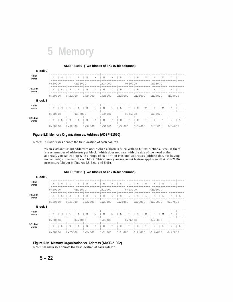
5 Memory
5 – 22
|--------------|--------------|--------------|--------------|--------------|----|| H | M | L | L | H | M | H | M | L | L | H | M | H | M | L | ||--------------|--------------|--------------|--------------|--------------|----|0x20000 0x22000 0x24000 0x26000 0x28000 |---------|---------|---------|---------|---------|---------|---------|---------|| H | L | H | L | H | L | H | L | H | L | H | L | H | L | H | L ||---------|---------|---------|---------|---------|---------|---------|---------|0x20000 0x22000 0x24000 0x26000 0x28000 0x2a000 0x2c000 0x2e000
|--------------|--------------|--------------|--------------|--------------|----|| H | M | L | L | H | M | H | M | L | L | H | M | H | M | L | ||--------------|--------------|--------------|--------------|--------------|----|0x30000 0x32000 0x34000 0x36000 0x38000 |---------|---------|---------|---------|---------|---------|---------|---------|| H | L | H | L | H | L | H | L | H | L | H | L | H | L | H | L ||---------|---------|---------|---------|---------|---------|---------|---------|0x30000 0x32000 0x34000 0x36000 0x38000 0x3a000 0x3c000 0x3e000
ADSP-21060 (Two blocks of 8Kx16-bit columns)
Block 0
48-bitwords
32/16-bitwords
Block 1
48-bitwords
32/16-bitwords
Figure 5.8 Memory Organization vs. Address (ADSP-21060)
Notes: All addresses denote the first location of each column.
“Non-existant” 48-bit addresses occur when a block is filled with 48-bit instructions. Because thereis a set number of addresses per block (which does not vary with the size of the word at theaddress), you can end up with a range of 48-bit “non-existant” addresses (addressable, but havingno contents) at the end of each block. This memory arrangement feature applies to all ADSP-2106xprocessors (shown in Figures 5.8, 5.9a, and 5.9b).
|--------------|--------------|--------------|--------------|--------------|----|| H | M | L | L | H | M | H | M | L | L | H | M | H | M | L | ||--------------|--------------|--------------|--------------|--------------|----|0x20000 0x21000 0x22000 0x23000 0x24000 |---------|---------|---------|---------|---------|---------|---------|---------|| H | L | H | L | H | L | H | L | H | L | H | L | H | L | H | L ||---------|---------|---------|---------|---------|---------|---------|---------|0x20000 0x21000 0x22000 0x23000 0x24000 0x25000 0x26000 0x27000
|--------------|--------------|--------------|--------------|--------------|----|| H | M | L | L | H | M | H | M | L | L | H | M | H | M | L | ||--------------|--------------|--------------|--------------|--------------|----|0x28000 0x29000 0x2a000 0x2b000 0x2c000 |---------|---------|---------|---------|---------|---------|---------|---------|| H | L | H | L | H | L | H | L | H | L | H | L | H | L | H | L ||---------|---------|---------|---------|---------|---------|---------|---------|0x28000 0x29000 0x2a000 0x2b000 0x2c000 0x2d000 0x2e000 0x2f000
Block 0
48-bitwords
32/16-bitwords
ADSP-21062 (Two blocks of 4Kx16-bit columns)
Block 1
48-bitwords
32/16-bitwords
Figure 5.9a Memory Organization vs. Address (ADSP-21062)Note: All addresses denote the first location of each column.
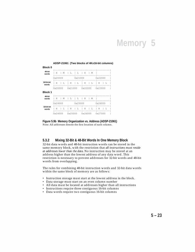
5Memory
5 – 23
Figure 5.9b Memory Organization vs. Address (ADSP-21061)Note: All addresses denote the first location of each column.
|--------------|--------------|---------|| H | M | L | L | H | M | | |--------------|--------------|---------|0x20000 0x21000 0x22000 | |---------|---------|---------|---------|| H | L | H | L | H | L | H | L | |---------|---------|---------|---------|0x20000 0x21000 0x22000 0x23000 |
|--------------|--------------|---------|| H | M | L | L | H | M | | |--------------|--------------|---------|0x24000 0x25000 0x26000 ||---------|---------|---------|---------|| H | L | H | L | H | L | H | L ||---------|---------|---------|---------|0x24000 0x25000 0x26000 0x27000 |
Block 0
48-bitwords
32/16-bitwords
ADSP-21061 (Two blocks of 4Kx16-bit columns)
Block 1
48-bitwords
32/16-bitwords
5.3.2 Mixing 32-Bit & 48-Bit Words In One Memory Block32-bit data words and 48-bit instruction words can be stored in thesame memory block, with the restriction that all instructions must resideat addresses lower than the data. No instruction may be stored at anaddress higher than the lowest address of any data word. Thisrestriction is necessary to prevent addresses for 32-bit words and 48-bitwords from overlapping.
The rules for combining 48-bit instruction words and 32-bit data wordswithin the same block of memory are as follows:
• Instruction storage must start at the lowest address in the block.• Data storage must start on an even column number• All data must be located at addresses higher than all instructions• Instructions require three contiguous 16-bit columns• Data words require two contiguous 16-bit columns
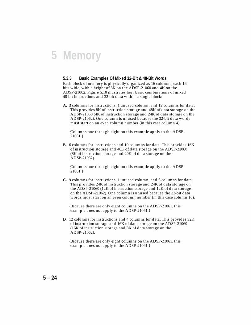
5 Memory
5 – 24
5.3.3 Basic Examples Of Mixed 32-Bit & 48-Bit WordsEach block of memory is physically organized as 16 columns, each 16bits wide, with a height of 8K on the ADSP-21060 and 4K on theADSP-21062. Figure 5.10 illustrates four basic combinations of mixed48-bit instructions and 32-bit data within a single block:
A. 3 columns for instructions, 1 unused column, and 12 columns for data.This provides 8K of instruction storage and 48K of data storage on theADSP-21060 (4K of instruction storage and 24K of data storage on theADSP-21062). One column is unused because the 32-bit data wordsmust start on an even column number (in this case column 4).
Columns one through eight on this example apply to the ADSP-21061.
B. 6 columns for instructions and 10 columns for data. This provides 16Kof instruction storage and 40K of data storage on the ADSP-21060(8K of instruction storage and 20K of data storage on theADSP-21062).
Columns one through eight on this example apply to the ADSP-21061.
C. 9 columns for instructions, 1 unused column, and 6 columns for data.This provides 24K of instruction storage and 24K of data storage onthe ADSP-21060 (12K of instruction storage and 12K of data storageon the ADSP-21062). One column is unused because the 32-bit datawords must start on an even column number (in this case column 10).
Because there are only eight columns on the ADSP-21061, thisexample does not apply to the ADSP-21061.
D. 12 columns for instructions and 4 columns for data. This provides 32Kof instruction storage and 16K of data storage on the ADSP-21060(16K of instruction storage and 8K of data storage on theADSP-21062).
Because there are only eight columns on the ADSP-21061, thisexample does not apply to the ADSP-21061.
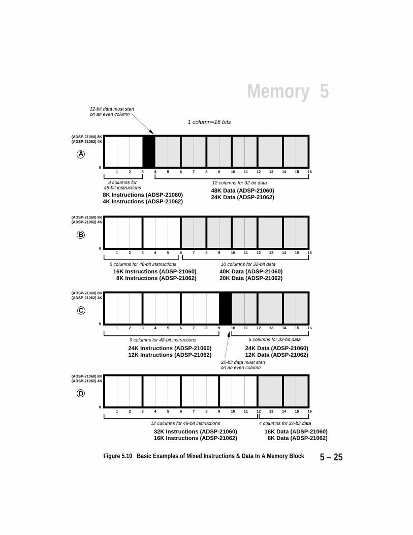
5Memory
5 – 25
0
3 columns for48-bit instructions
1 2 3 4 5 6 7 8 9 10 11 12 13 14 15 16
12 columns for 32-bit data
1 column=16 bits
32-bit data must start on an even column
9 columns for 48-bit instructions
01 2 3 4 5 6 7 8 9 10 11 12 13 14 15 16
6 columns for 32-bit data
12 columns for 48-bit instructions
01 2 3 4 5 6 7 8 9 10 11 12 13 14 15 16
4 columns for 32-bit data
32-bit data must start on an even column
0
6 columns for 48-bit instructions
1 2 3 4 5 6 7 8 9 10 11 12 13 14 15 16
10 columns for 32-bit data
A
B
C
D
8K Instructions (ADSP-21060)4K Instructions (ADSP-21062)
(ADSP-21060) 8K (ADSP-21062) 4K
(ADSP-21060) 8K (ADSP-21062) 4K
(ADSP-21060) 8K (ADSP-21062) 4K
(ADSP-21060) 8K (ADSP-21062) 4K
48K Data (ADSP-21060)24K Data (ADSP-21062)
16K Instructions (ADSP-21060) 8K Instructions (ADSP-21062)
40K Data (ADSP-21060)20K Data (ADSP-21062)
24K Instructions (ADSP-21060)12K Instructions (ADSP-21062)
24K Data (ADSP-21060)12K Data (ADSP-21062)
32K Instructions (ADSP-21060)16K Instructions (ADSP-21062)
16K Data (ADSP-21060) 8K Data (ADSP-21062)
Figure 5.10 Basic Examples of Mixed Instructions & Data In A Memory Block
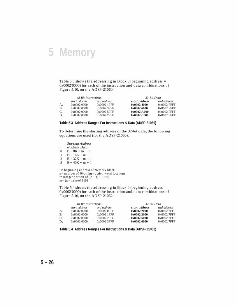
5 Memory
5 – 26
Table 5.3 shows the addressing in Block 0 (beginning address =0x0002 0000) for each of the instruction and data combinations ofFigure 5.10, on the ADSP-21060:
48-Bit Instructions 32-Bit Datastart address end address start address end address
A. 0x0002 0000 0x0002 1FFF 0x0002 4000 0x0002 FFFFB. 0x0002 0000 0x0002 3FFF 0x0002 6000 0x0002 FFFFC. 0x0002 0000 0x0002 5FFF 0x0002 A000 0x0002 FFFFD. 0x0002 0000 0x0002 7FFF 0x0002 C000 0x0002 FFFF
Table 5.3 Address Ranges For Instructions & Data (ADSP-21060)
To determine the starting address of the 32-bit data, the followingequations are used (for the ADSP-21060):
Starting Address i of 32-Bit Data 0 B + 8K + m + 1 1 B + 16K + m + 1 2 B + 32K + m + 1 3 B + 40K + m + 1
B= beginning address of memory blockn= number of 48-bit instruction word locationsi= integer portion of [(n – 1) ÷ 8192]m= (n – 1) mod 8192
Table 5.4 shows the addressing in Block 0 (beginning address =0x0002 0000) for each of the instruction and data combinations ofFigure 5.10, on the ADSP-21062:
48-Bit Instructions 32-Bit Datastart address end address start address end address
A. 0x0002 0000 0x0002 0FFF 0x0002 2000 0x0002 7FFFB. 0x0002 0000 0x0002 1FFF 0x0002 3000 0x0002 7FFFC. 0x0002 0000 0x0002 2FFF 0x0002 5000 0x0002 7FFFD. 0x0002 0000 0x0002 3FFF 0x0002 6000 0x0002 7FFF
Table 5.4 Address Ranges For Instructions & Data (ADSP-21062)

5Memory
5 – 27
To determine the starting address of the 32-bit data, the followingequations are used (for the ADSP-21062 and ADSP-21061):
Starting Address i of 32-Bit Data 0 B + 4K + m + 1 1 B + 8K + m + 1 2 B + 16K + m + 1 3 B + 20K + m + 1
B = beginning address of memory blockn = number of 48-bit instruction word locationsi = integer portion of [(n – 1) ÷ 4096]m = (n – 1) mod 4096
5.3.4 16-Bit Short WordsNormal word addressing is used for accesses of 32-bit or 48-bit words.All instruction fetches and 32-bit data accesses are accomplished withnormal word addresses. Short word addresses can be used, however,to access 16-bit data. Short word addressing increases the amount of16-bit data that can be stored in internal memory, and also allowsMSW (most significant word) and LSW (least significant word)addressing of 32-bit words. Bit 0 of the address selects between theMSW and LSW of the 32-bit word.
A single location in memory (i.e. the lower 16 bits of a 32-bit word) canbe accessed in two ways: with a normal word address or a short wordaddress. The short word address is a left shift of the correspondingnormal word address. This allows easy conversion between shortword address and normal word address for the same physical location.Figure 5.11 shows how the short word addresses are related to normalword addresses for 32-bit words. (Figures 5.9 and 5.10 show how theseaddresses are related to normal word addresses for 48-bit words.) Notethat the 16-bit data words are transferred over lines 31-16 of theinternal PM Data Bus and DM Data Bus as well as the external bus(DATA47-0)
Arithmetically shifting a short word address to the right by one bitproduces the corresponding normal word address. Arithmeticallyshifting a normal word address to the left produces the short wordaddress of the LSW of the 32-bit normal word. To generate the shortword address of the MSW, the left shift is performed and bit 0 is thenset to 1.
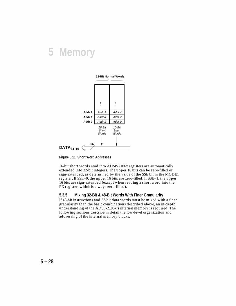
5 Memory
5 – 28
Addr 1
Addr 3
Addr 5
Addr 0
Addr 2
Addr 4
DATA31-16
16
... ...
16-Bit Short
Words
32-Bit Normal Words
16-Bit Short Words
Addr 0
Addr 1
Addr 2
Figure 5.11 Short Word Addresses
16-bit short words read into ADSP-2106x registers are automaticallyextended into 32-bit integers. The upper 16 bits can be zero-filled orsign-extended, as determined by the value of the SSE bit in the MODE1register. If SSE=0, the upper 16 bits are zero-filled. If SSE=1, the upper16 bits are sign-extended (except when reading a short word into thePX register, which is always zero-filled).
5.3.5 Mixing 32-Bit & 48-Bit Words With Finer GranularityIf 48-bit instructions and 32-bit data words must be mixed with a finergranularity than the basic combinations described above, an in-depthunderstanding of the ADSP-2106x’s internal memory is required. Thefollowing sections describe in detail the low-level organization andaddressing of the internal memory blocks.

5Memory
5 – 29
5.3.5.1 Low-Level Physical Mapping Of Memory BlocksEach block of memory is organized as 16 columns. On the ADSP-21060,each column contains 8K 16-bit words; on the ADSP-21062, each columncontains 4K 16-bit words. For reads or writes of 48-bit and 32-bit words,the 13 LSBs of the address select a row from each column. The MSBs ofthe address control which columns are selected. For reads or writes of16-bit short words, the address is right-shifted one place before beingapplied to memory (see Figure 5.12). This allows bit 0 of the address tobe used to select between the MSW and LSW of 32-bit data.
When a block is memory is accessed, how many and which columns areselected depends upon the word width of the access. For 48-bit words,the 16-bit columns are selected in groups of three and address bits 13-15determine which group is selected. For 32-bit words, the columns areselected in groups of two and address bits 13-15 also select the group.
16-bit short word accesses are handled in a slightly different fashion, inorder to provide easy access to the MSW and LSW of 32-bit data. In theADSP-2106x’s data address generators (DAGs), a single arithmetic rightshift of the short word address gives the physical address of the 32-bitword being written to. If the bit shifted out is zero, the access is to theLSW, otherwise it is to the MSW. This is implemented by selectingcolumns in groups of two with address bits 13-15 and then selectingbetween the two columns in the group with the short word address bitshifted out.
Figure 5.12 Preprocessing of 16-Bit Short Word Addresses
Shift Right
017 16 152431
1110 0001
15 0
High/LowWord (16-bit) Select
Short Word Address
Physical Address Appliedto Memory Block
Block Select
13 12
Row AddressColumnAddress
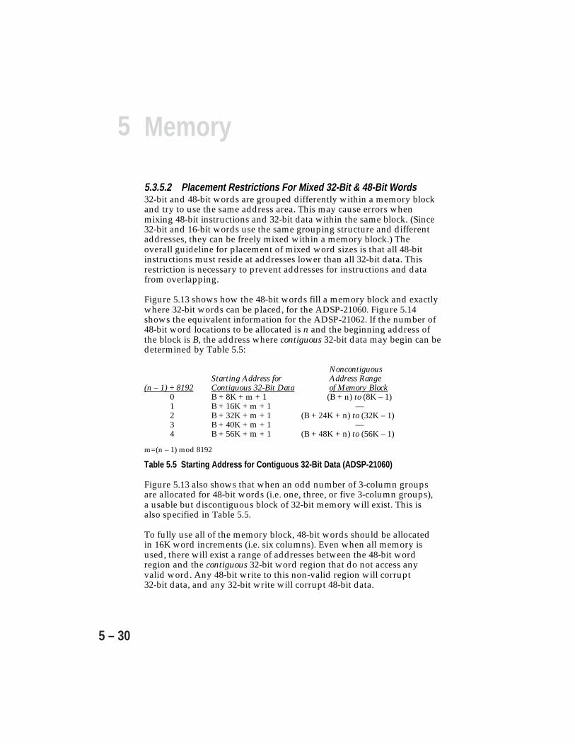
5 Memory
5 – 30
5.3.5.2 Placement Restrictions For Mixed 32-Bit & 48-Bit Words32-bit and 48-bit words are grouped differently within a memory blockand try to use the same address area. This may cause errors whenmixing 48-bit instructions and 32-bit data within the same block. (Since32-bit and 16-bit words use the same grouping structure and differentaddresses, they can be freely mixed within a memory block.) Theoverall guideline for placement of mixed word sizes is that all 48-bitinstructions must reside at addresses lower than all 32-bit data. Thisrestriction is necessary to prevent addresses for instructions and datafrom overlapping.
Figure 5.13 shows how the 48-bit words fill a memory block and exactlywhere 32-bit words can be placed, for the ADSP-21060. Figure 5.14shows the equivalent information for the ADSP-21062. If the number of48-bit word locations to be allocated is n and the beginning address ofthe block is B, the address where contiguous 32-bit data may begin can bedetermined by Table 5.5:
NoncontiguousStarting Address for Address Range
(n – 1) ÷ 8192 Contiguous 32-Bit Data of Memory Block0 B + 8K + m + 1 (B + n) to (8K – 1)1 B + 16K + m + 1 —2 B + 32K + m + 1 (B + 24K + n) to (32K – 1)3 B + 40K + m + 1 —4 B + 56K + m + 1 (B + 48K + n) to (56K – 1)
m=(n – 1) mod 8192
Table 5.5 Starting Address for Contiguous 32-Bit Data (ADSP-21060)
Figure 5.13 also shows that when an odd number of 3-column groupsare allocated for 48-bit words (i.e. one, three, or five 3-column groups),a usable but discontiguous block of 32-bit memory will exist. This isalso specified in Table 5.5.
To fully use all of the memory block, 48-bit words should be allocatedin 16K word increments (i.e. six columns). Even when all memory isused, there will exist a range of addresses between the 48-bit wordregion and the contiguous 32-bit word region that do not access anyvalid word. Any 48-bit write to this non-valid region will corrupt32-bit data, and any 32-bit write will corrupt 48-bit data.
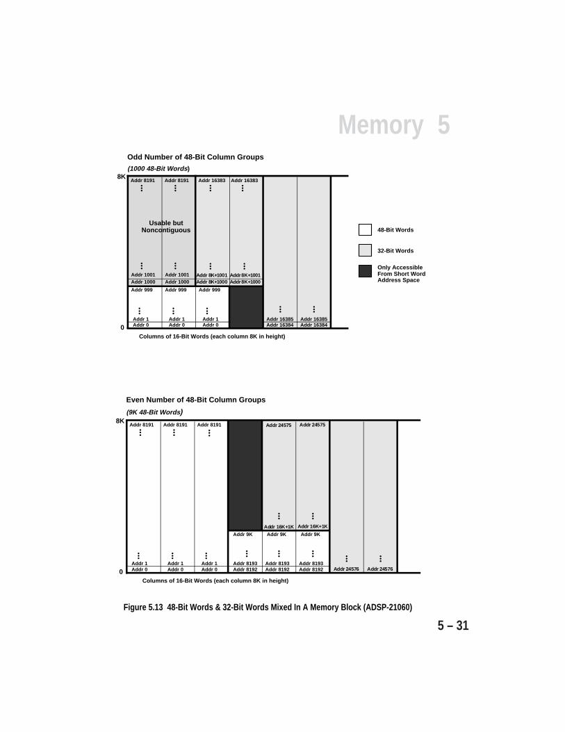
5Memory
5 – 31Figure 5.13 48-Bit Words & 32-Bit Words Mixed In A Memory Block (ADSP-21060)
Only Accessible From Short Word Address Space
48-Bit Words
32-Bit Words
Odd Number of 48-Bit Column Groups
(1000 48-Bit Words)
Addr 0Addr 1
Addr 999
Addr 0Addr 1
Addr 999
Addr 0Addr 1
Addr 999
Addr 8191 Addr 8191 Addr 16383
Columns of 16-Bit Words (each column 8K in height)
8KAddr 16383
Addr 8K+1000
Addr 16384 Addr 16384Addr 16385 Addr 16385
0
...
... ...... ... ...
Addr 1000 Addr 1000Addr 1001 Addr 1001
... ...
... ...
Usable but Noncontiguous
Addr 8K+1000Addr 8K+1001 Addr 8K+1001
... ...
...
Addr 0Addr 1
Addr 0Addr 1
Addr 0Addr 1
Addr 8191 Addr 8191 Addr 8191
Columns of 16-Bit Words (each column 8K in height)
8K
Addr 8192 Addr 8192Addr 8193 Addr 8193
0
Even Number of 48-Bit Column Groups
(9K 48-Bit Words)
... ...... ... ...
... ...
Addr 16K+1K Addr 16K+1K
...
Addr 8192Addr 8193
...
Addr 9K Addr 9K Addr 9K
... ...
Addr 24575 Addr 24575
Addr 24576 Addr 24576
... ...

5 Memory
5 – 32
Only Accessible From Short Word Address Space
48-Bit Words
32-Bit Words
Odd Number of 48-Bit Column Groups
(1000 48-Bit Words)
Addr 0Addr 1
Addr 999
Addr 0Addr 1
Addr 999
Addr 0Addr 1
Addr 999
Addr 4095 Addr 4095 Addr 8191
Columns of 16-Bit Words (each column 4K in height)
4KAddr 8191
Addr 4K+1000
Addr 8192 Addr 8192Addr 8193 Addr 8193
0
...
... ...... ... ...
Addr 1000 Addr 1000Addr 1001 Addr 1001
... ...
... ...
Usable but Noncontiguous
Addr 4K+1000Addr 4K+1001 Addr 4K+1001
... ...
...
Addr 0Addr 1
Addr 0Addr 1
Addr 0Addr 1
Addr 4095 Addr 4095 Addr 4095 4K
Addr 4096 Addr 4096Addr 4097 Addr 4097
0
Even Number of 48-Bit Column Groups
(5K 48-Bit Words)
... ...... ... ...
... ...
Addr 8K+1K Addr 8K+1K
...
Addr 4096Addr 4097
...
Addr 5K Addr 5K Addr 5K
... ...
Addr 12K Addr 12K
Addr 12K Addr 12K
... ...
Columns of 16-Bit Words (each column 4K in height)
Figure 5.14 48-Bit Words & 32-Bit Words Mixed In A Memory Block (ADSP-21062 or ADSP-21061)
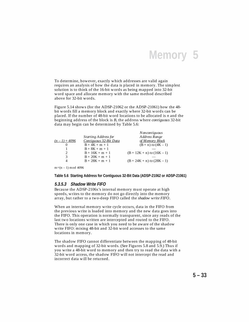
5Memory
5 – 33
To determine, however, exactly which addresses are valid againrequires an analysis of how the data is placed in memory. The simplestsolution is to think of the 16-bit words as being mapped into 32-bitword space and allocate memory with the same method describedabove for 32-bit words.
Figure 5.14 shows (for the ADSP-21062 or the ADSP-21061) how the 48-bit words fill a memory block and exactly where 32-bit words can beplaced. If the number of 48-bit word locations to be allocated is n and thebeginning address of the block is B, the address where contiguous 32-bitdata may begin can be determined by Table 5.6:
NoncontiguousStarting Address for Address Range
(n – 1) ÷ 4096 Contiguous 32-Bit Data of Memory Block0 B + 4K + m + 1 (B + n) to (4K – 1)1 B + 8K + m + 1 —2 B + 16K + m + 1 (B + 12K + n) to (16K – 1)3 B + 20K + m + 1 —4 B + 28K + m + 1 (B + 24K + n) to (28K – 1)
m=(n – 1) mod 4096
Table 5.6 Starting Address for Contiguous 32-Bit Data (ADSP-21062 or ADSP-21061)
5.3.5.3 Shadow Write FIFOBecause the ADSP-2106x’s internal memory must operate at highspeeds, writes to the memory do not go directly into the memoryarray, but rather to a two-deep FIFO called the shadow write FIFO.
When an internal memory write cycle occurs, data in the FIFO fromthe previous write is loaded into memory and the new data goes intothe FIFO. This operation is normally transparent, since any reads of thelast two locations written are intercepted and routed to the FIFO.There is only one case in which you need to be aware of the shadowwrite FIFO: mixing 48-bit and 32-bit word accesses to the samelocations in memory.
The shadow FIFO cannot differentiate between the mapping of 48-bitwords and mapping of 32-bit words. (See Figures 5.8 and 5.9.) Thus ifyou write a 48-bit word to memory and then try to read the data with a32-bit word access, the shadow FIFO will not intercept the read andincorrect data will be returned.

5 Memory
5 – 34
If 48-bit accesses and 32-bit accesses to the same locations absolutelymust be mixed in this way, you must flush out the shadow FIFO withtwo dummy writes before attempting to read the data.
5.3.6 Configuring Memory For 32-Bit or 40-Bit DataEach block of internal memory can be configured to store either single-precision 32-bit data or extended-precision 40-bit data. Thisconfiguration is selected by setting or clearing the IMDW0 and IMDW1bits in the SYSCON register. If the IMDWx bit is equal to zero, 32-bitdata is selected; when a data access occurs, a 32-bit access isperformed. If the IMDWx bit is equal to one, 40-bit data is selected;when a data access occurs, a 48-bit access is performed.
If an ADSP-2106x program attempts to write 40-bit data (in a 48-bitword) to a memory block configured for 32-bit data, the lower 16 bits(of the 48-bit word) are truncated. If a 40-bit data read is attempted, thelower 8 bits will be zeros. The PX register is the only exception to theserules—all read/writes of the PX register are performed as 48-bitaccesses. If any 40-bit data must be stored in a memory blockconfigured for 32-bit words, the PX register should be used to accessthe 40-bit data in 48-bit words. For 48-bit writes of this kind, from thePX register to 32-bit memory, be sure that the physical memory spaceof the 48-bit destination does not corrupt any 32-bit data.
Changing the value of the IMDWx bits during system operation ispossible, but be aware that any kind of memory access will be affected.This includes ADSP-2106x–to–ADSP-2106x direct read/writes, hostprocessor–to–ADSP-2106x direct read/writes, DMA transfers, andinterrupt data areas.
(Note that the word width of data accesses is not related to the value ofthe arithmetic precision mode bit, RND32. This allows the occasionaluse of 32-bit data in extended-precision 40-bit systems, without havingto toggle the value of RND32 in your program.)
Because the ADSP-2106x’s memory blocks must be configured foreither 32-bit or 40-bit data, DMA transfers automatically read or writethe proper word width. This simplifies setting up DMA channels for asystem. DMA transfers between serial ports and memory are limited toa 32-bit word width (maximum).
(Note also that 32-bit words and 16-bit short words can be freely mixedin the same memory block, with no restrictions.)

5Memory
5 – 35
5.4 EXTERNAL MEMORY INTERFACINGIn addition to its on-chip SRAM, the ADSP-2106x provides addressing ofup to 4 gigawords of off-chip memory through its external port. Thisexternal address space includes multiprocessor memory space, the on-chipmemory of all other ADSP-2106xs connected in a multiprocessor system,as well as external memory space, the region for standard addressing ofoff-chip memory.
Table 5.7 defines the ADSP-2106x pins used for interfacing to externalmemory. Memory control signals allow direct connection to fast staticRAM devices. Memory-mapped peripherals and slower memories arealso supported, with a user-defined combination of programmable waitstates and hardware acknowledge signals. The suspend bus tristate pin(SBTS) and page boundary pin (PAGE) can be used with DRAMmemory.
External memory can hold both instructions and data. The externaldata bus (DATA47-0) must be 48 bits wide to transfer instructionsand/or 40-bit extended-precision floating-point data, or 32 bits wide totransfer single-precision floating-point data. If external memorycontains only data or packed instructions that will be transferred byDMA, the external data bus width can be either 16 or 32 bits. In thistype of system, the ADSP-2106x’s on-chip I/O processor handlesunpacking operations on data coming into it and packing operationson data going out. Figure 5.a shows how different data word sizes aretransferred over the external port.
081624324047
DATA47-0
EPROMBoot
16-Bit Packed
32-Bit Float or Fixed,D31 - D0,
32-Bit Packed
40-Bit Extended Float
Instruction Fetch
Figure 5.a External Port Data Alignment

5 Memory
5 – 36
The internal 32-bit DM Address bus and the I/O processor can accessthe entire 4-gigaword external memory space. The 24-bit PM Addressbus, however, can only access 12 megawords of external memorybecause of its smaller width.Pin Type FunctionADDR31-0 I/O/T External Bus Address. The ADSP-2106x outputs addresses for
external memory and peripherals on these pins. In amultiprocessor system the bus master outputs addresses forread/writes of the internal memory or IOP registers of otherADSP-2106xs. The ADSP-2106x inputs addresses when a hostprocessor or multiprocessing bus master is reading or writingits internal memory or IOP registers.
DATA47-0 I/O/T External Bus Data. The ADSP-2106x inputs and outputs dataand instructions on these pins. 32-bit single-precision floating-point data and 32-bit fixed-point data is transferred over bits47-16 of the bus. 40-bit extended-precision floating-point datais transferred over bits 47-8 of the bus. 16-bit short word datais transferred over bits 31-16 of the bus. Pull-up resistors onunused DATA pins are not necessary.
MS3-0 O/T Memory Select Lines. These lines are asserted (low) as chipselects for the corresponding banks of external memory.Memory bank size must be defined in the ADSP-2106x’ssystem control register (SYSCON). The MS3-0 lines aredecoded memory address lines that change at the same time asthe other address lines. When no external memory access isoccurring the MS3-0 lines are inactive; they are active,however, when a conditional memory access instruction isexecuted, whether or not the condition is true. MS0 can beused with the PAGE signal to implement a bank of DRAMmemory (Bank 0). In a multiprocessing system the MS3-0 linesare output by the bus master.
RD I/O/T Memory Read Strobe. This pin is asserted (low) when theADSP-2106x reads from external memory devices or from theinternal memory of other ADSP-2106xs. External devices(including other ADSP-2106xs) must assert RD to read fromthe ADSP-2106x’s internal memory. In a multiprocessingsystem RD is output by the bus master and is input by allother ADSP-2106xs.
Table 5.7 External Memory Interface Signals (cont. on next page)
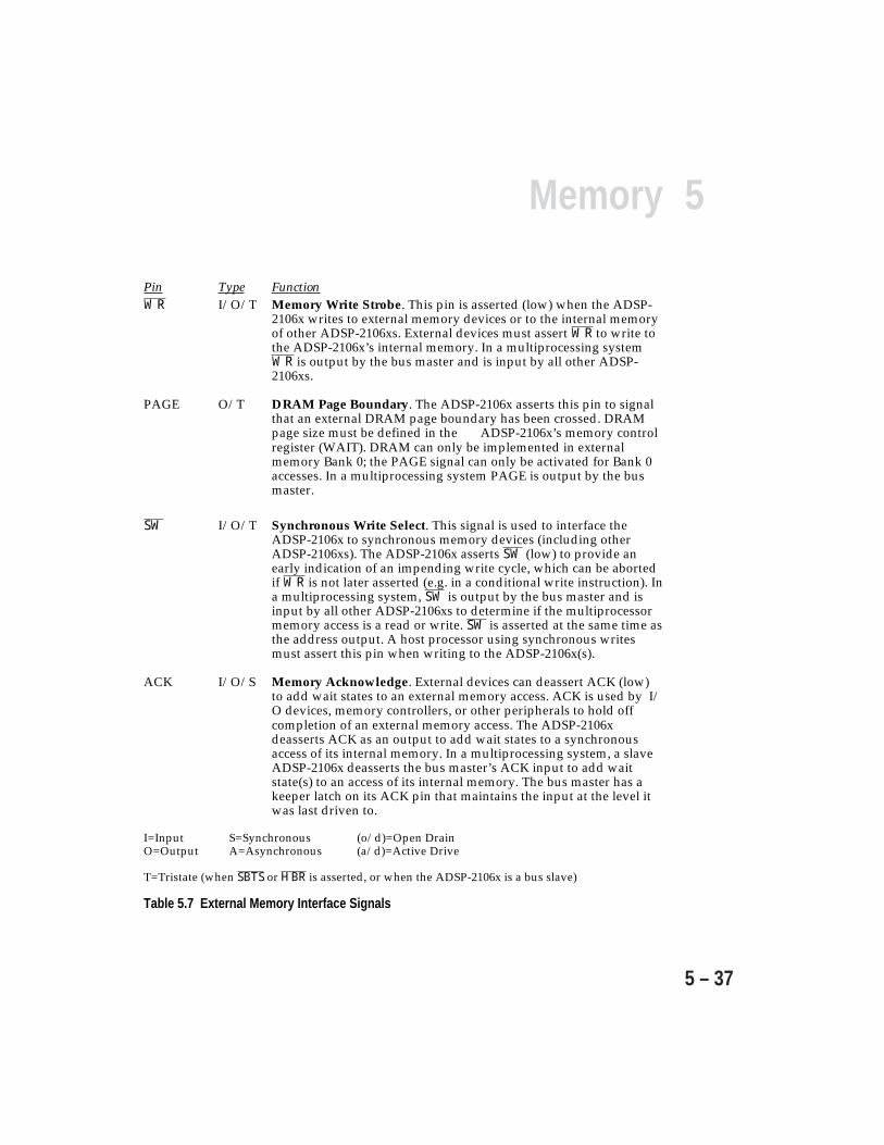
5Memory
5 – 37
Pin Type FunctionWR I/O/T Memory Write Strobe. This pin is asserted (low) when the ADSP-
2106x writes to external memory devices or to the internal memoryof other ADSP-2106xs. External devices must assert WR to write tothe ADSP-2106x’s internal memory. In a multiprocessing systemWR is output by the bus master and is input by all other ADSP-2106xs.
PAGE O/T DRAM Page Boundary. The ADSP-2106x asserts this pin to signalthat an external DRAM page boundary has been crossed. DRAMpage size must be defined in the ADSP-2106x’s memory controlregister (WAIT). DRAM can only be implemented in externalmemory Bank 0; the PAGE signal can only be activated for Bank 0accesses. In a multiprocessing system PAGE is output by the busmaster.
SW I/O/T Synchronous Write Select. This signal is used to interface theADSP-2106x to synchronous memory devices (including otherADSP-2106xs). The ADSP-2106x asserts SW (low) to provide anearly indication of an impending write cycle, which can be abortedif WR is not later asserted (e.g. in a conditional write instruction). Ina multiprocessing system, SW is output by the bus master and isinput by all other ADSP-2106xs to determine if the multiprocessormemory access is a read or write. SW is asserted at the same time asthe address output. A host processor using synchronous writesmust assert this pin when writing to the ADSP-2106x(s).
ACK I/O/S Memory Acknowledge. External devices can deassert ACK (low)to add wait states to an external memory access. ACK is used by I/O devices, memory controllers, or other peripherals to hold offcompletion of an external memory access. The ADSP-2106xdeasserts ACK as an output to add wait states to a synchronousaccess of its internal memory. In a multiprocessing system, a slaveADSP-2106x deasserts the bus master’s ACK input to add waitstate(s) to an access of its internal memory. The bus master has akeeper latch on its ACK pin that maintains the input at the level itwas last driven to.
I=Input S=Synchronous (o/d)=Open DrainO=Output A=Asynchronous (a/d)=Active Drive
T=Tristate (when SBTS or HBR is asserted, or when the ADSP-2106x is a bus slave)
Table 5.7 External Memory Interface Signals
5 Memory
5 – 38
5.4.1 External Memory BanksExternal memory is divided into four banks of equal size, eachassociated with its own wait-state generator. This allows slowerperipheral devices to be memory-mapped into a bank for which aspecific number of wait states are specified. By mapping peripheralsinto different banks, you can accommodate I/O devices with differenttiming requirements.
Bank 0 starts at address 0x0040 0000 in external memory and isfollowed in order by Banks 1, 2, and 3. Whenever the ADSP-2106xgenerates an address located within one of the four banks, thecorresponding memory select line, MS3-0, is asserted.
The MS3-0 outputs can be used as chip selects for memories or otherexternal devices, eliminating the need for external decoding logic. MS0provides a select line for a bank of DRAM memory, when used incombination with the PAGE signal (see “DRAM Page BoundaryDetection”).
The size of the memory banks can range from 8K words to 256megawords, and must be a power of two. Selection of memory banksize is accomplished by setting the MSIZE bit field of the SYSCONregister in the following way:
MSIZE = log2 (desired bank size) – 13
The MS3-0 lines are decoded memory address lines that change at thesame time as the other address lines. When no external memory accessis occurring the MS3-0 lines are inactive; they are active, however,when a conditional memory access instruction is executed, whether ornot the condition is true. Systems using the SW signal that cannot abortsuch accesses should not use conditional memory write instructions, toensure proper operation.
(Note that the ADSP-2106x’s internal memory is divided into twoblocks, called Block 0 and Block 1, while the external memory space isdivided into four banks.)
5.4.2 Unbanked MemoryThe region of memory above Banks 0-3 is called unbanked externalmemory space. No MSx memory select line is asserted for accesses inthis address space. Unbanked memory space accesses can also havewait states specified, in the UBWS and UBWM fields of the WAITregister.

5Memory
5 – 39
5.4.3 Boot Memory Select (BMSBMS)The BMS memory select line is asserted (low) only when the ADSP-2106x is configured for EPROM booting. This allows access of aseparate external memory space for booting. Unbanked memory waitstates and wait state mode are applied to BMS-selected accesses.
The BMS output is only driven by the ADSP-2106x bus master. Fordetails on EPROM booting, see “Booting” in the System Design chapterof this manual.
5.4.4 Wait States & AcknowledgeThe ADSP-2106x’s WAIT register is used to set up external memorywait states and response to the ACK signal. The WAIT register is oneof the ADSP-2106x’s IOP control registers.
To simplify the interface to slow external memories and peripherals,the ADSP-2106x provides a variety of methods for extending off-chipmemory accesses:
• External. The ADSP-2106x samples its acknowledge input (ACK)during each clock cycle. If it latches a low value, it inserts a wait state byholding the address and strobes valid for an additional cycle. If thevalue of ACK is high, the ADSP-2106x completes the cycle.
• Internal. The ADSP-2106x ignores the ACK input. Control bits in theWAIT register specify the number of wait states for the access. You canspecify a different number of wait states for each bank of externalmemory.
• Both. The ADSP-2106x samples its ACK input in each clock cycle. If itlatches a low value, it inserts a wait state. If the value of ACK is high, itcompletes the cycle only if the number of wait states (specified inWAIT) have expired. In this mode, the WAIT-programmed wait statesspecify a minimum number of cycles per access, and an external devicecan use the ACK pin to extend the access as necessary. The ACK signalmay be undefined (transitioning) until the internally programmedwaitstates have completed; i.e. ACK is not sampled until theprogrammed waitstates have completed. No metastability problemswill occur.
5 Memory
5 – 40
• Either. The ADSP-2106x completes the cycle as soon as it samples the ACKinput as high or when the WAIT-programmed number of wait states haveexpired, whichever occurs first. In this mode, a system with two differenttypes of peripherals could shorten the access for the faster peripheral usingACK but use the programmed wait states for the slower peripheral.
The method selected for each bank of memory is independent of the otherbanks. Thus, you can map devices of different speeds into differentmemory banks for the appropriate wait state control.
5.4.4.1 WAIT RegisterThe WAIT register is defined in Table 5.8 and shown in Figure 5.15. Thebit values shown in Figure 5.15 are the default initialization; the WAITregister is initialized to 0x21AD 6B5A after a processor reset.
A bus idle cycle is an inactive bus cycle that is automatically generated toavoid bus driver conflicts. Such a conflict can occur when a device with along output disable time continues to drive after RD is deasserted whileanother device begins driving in the following cycle.
To avoid this conflict, the ADSP-2106x will generate an inactive bus cycleon a transition from a read of a memory bank with bus idle cycle enabledto an access of any other bank or to a write in the same bank or to MMS(multiprocessor memory space). In other words, a bus idle cycle is alwaysgenerated after a read, except in the case of consecutive reads of the samebank. A device with a slow disable time should enable bus idle cyclegeneration by using # of wait states code 001, 010, 011, or 111.
When a bus idle cycle is specified for unbanked memory, an idle cycle isinserted after every read cycle, not just after a bank change. This allowsseveral external devices to be used in this region of memory. The ADSP-2106x cannot distinguish when there is a device change so it inserts an idlecycle after each read.
A hold time cycle is an inactive bus cycle automatically generated at the endof a read or write to allow a longer hold time for address and data. Theaddress and data will remain unchanged and driven for one cycle after theread or write strobes are deasserted.
A single idle cycle on a page boundary crossing can be enabled by settingthe PAGEIS bit of the WAIT register; the address is asserted in the samecycle that the PAGE pin is asserted, but read/write strobe assertion isdelayed for one cycle. See “DRAM Page Boundary Detection” for furtherdetails.
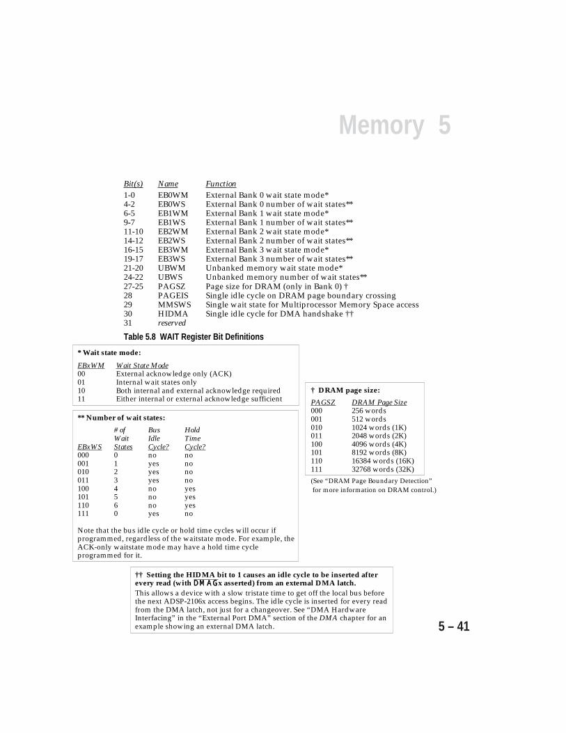
5Memory
5 – 41
Bit(s) Name Function1-0 EB0WM External Bank 0 wait state mode*4-2 EB0WS External Bank 0 number of wait states**6-5 EB1WM External Bank 1 wait state mode*9-7 EB1WS External Bank 1 number of wait states**11-10 EB2WM External Bank 2 wait state mode*14-12 EB2WS External Bank 2 number of wait states**16-15 EB3WM External Bank 3 wait state mode*19-17 EB3WS External Bank 3 number of wait states**21-20 UBWM Unbanked memory wait state mode*24-22 UBWS Unbanked memory number of wait states**27-25 PAGSZ Page size for DRAM (only in Bank 0) †28 PAGEIS Single idle cycle on DRAM page boundary crossing29 MMSWS Single wait state for Multiprocessor Memory Space access30 HIDMA Single idle cycle for DMA handshake ††31 reserved
Table 5.8 WAIT Register Bit Definitions
† DRAM page size:
PAGSZ DRAM Page Size000 256 words001 512 words010 1024 words (1K)011 2048 words (2K)100 4096 words (4K)101 8192 words (8K)110 16384 words (16K)111 32768 words (32K)(See “DRAM Page Boundary Detection” for more information on DRAM control.)
* Wait state mode:
EBxWM Wait State Mode00 External acknowledge only (ACK)01 Internal wait states only10 Both internal and external acknowledge required11 Either internal or external acknowledge sufficient
** Number of wait states:
# of Bus HoldWait Idle Time
EBxWS States Cycle? Cycle?000 0 no no001 1 yes no010 2 yes no011 3 yes no100 4 no yes101 5 no yes110 6 no yes111 0 yes no
Note that the bus idle cycle or hold time cycles will occur ifprogrammed, regardless of the waitstate mode. For example, theACK-only waitstate mode may have a hold time cycleprogrammed for it.
†† Setting the HIDMA bit to 1 causes an idle cycle to be inserted afterevery read (with DMAGDMAGx asserted) from an external DMA latch.This allows a device with a slow tristate time to get off the local bus beforethe next ADSP-2106x access begins. The idle cycle is inserted for every readfrom the DMA latch, not just for a changeover. See “DMA HardwareInterfacing” in the “External Port DMA” section of the DMA chapter for anexample showing an external DMA latch.
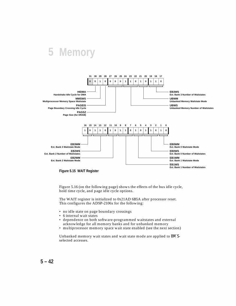
5 Memory
5 – 42
11 10 9 8 7 6 5 4 3 2 1 0
010110101101
15 14 13 12
0110
EB0WMExt. Bank 0 Waitstate Mode
EB0WSExt. Bank 0 Number of Waitstates
EB1WMExt. Bank 1 Waitstate Mode
EB1WSExt. Bank 1 Number of Waitstates
16
EB3WMExt. Bank 3 Waitstate Mode
EB2WSExt. Bank 2 Number of Waitstates
EB2WMExt. Bank 2 Waitstate Mode
26 25 24 23 22 21 20 19 18 17
01101011000
31 30 29 28 27
0100
EB3WSExt. Bank 3 Number of Waitstates
UBWMUnbanked Memory Waitstate Mode
UBWSUnbanked Memory Number of Waitstates
HIDMAHandshake Idle Cycle for DMA
MMSWSMultiprocessor Memory Space Waitstate
PAGEIS Page Boundary Crossing Idle Cycle
PAGSZ Page Size (for DRAM)
1
Figure 5.15 WAIT Register
Figure 5.16 (on the following page) shows the effects of the bus idle cycle,hold time cycle, and page idle cycle options.
The WAIT register is initialized to 0x21AD 6B5A after processor reset.This configures the ADSP-2106x for the following:
• no idle state on page boundary crossings• 6 internal wait states• dependence on both software-programmed waitstates and external
acknowledge for all memory banks and for unbanked memory• multiprocessor memory space wait state enabled (see the next section)
Unbanked memory wait states and wait state mode are applied to BMS-selected accesses.
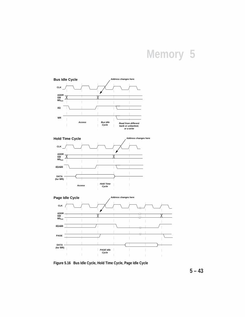
5Memory
5 – 43Figure 5.16 Bus Idle Cycle, Hold Time Cycle, Page Idle Cycle
CLK
RD
ADDRSWMS3-0
WR
Access Bus Idle Cycle
Read from different bank or unbanked,
or a write
Bus Idle Cycle Address changes here
CLK
ADDRSWMS3-0
Access Hold Time
Cycle
Hold Time Cycle
RD/WR
Address changes here
DATA(for WR)
CLK
ADDRSWMS3-0
PAGE Idle Cycle
Page Idle Cycle
RD/WR
PAGE
Address changes here
DATA(for WR)
5 Memory
5 – 44
5.4.4.2 Multiprocessor Memory Space Wait States & AcknowledgeCompletion of reads and writes to multiprocessor memory space dependsonly on the ACK signal. This is facilitated by using the SW signal as anearly indication of whether the access is a write or a read (see Figure 5.19 atthe end of this chapter), as well as the use of the automatic wait state optionfor multiprocessor memory space—the MMSWS bit of the WAIT register.
Setting the MMSWS bit (bit 29) of the WAIT register causes the insertion ofa single wait state into all multiprocessor memory space reads and writes.This option should be used whenever the external system bus is heavilyloaded (i.e. such that the synchronous timing requirements for interprocessorcommunications cannot be met; refer to the ADSP-2106x Data Sheet for thesespecifications.)
The ADSP-2106x bus master inserts the wait state. The slave ADSP-2106x(s)respond with ACK (low) in the first cycle, even if they have MMSWS=1. IfMMSWS=1 on the master ADSP-2106x, it will ignore ACK in the first cycle andrespond to it in the second cycle. This setting allows longer set up times for thefollowing slave SHARC’s signals: ADDR, RD, WR, and DATA (written to theslave). Also, this setting allows a longer set up time for the master SHARC’sACK signal. Other hold and set up times are not influenced by MMSWS=1.This setting does not change hold time requirements for the slave SHARC’sRD, WR, or DATA (written to the slave). Also, this setting does not change themaster SHARC’s set up or hold times for DATA (read from the slave).
All of the ADSP-2106xs in a multiprocessor system must have the samevalue for the MMSWS bit.
5.4.5 DRAM Page Boundary DetectionApplications with large amounts of data may want to use DRAM memoryfor bulk storage. To simplify interfacing to page-mode or static-columnDRAMs, the ADSP-2106x detects page boundary crossings and outputsthe PAGE signal to an external DRAM controller. Page boundaries are user-defined; they must be programmed in the WAIT register.
Automatic page boundary detection is provided by the ADSP-2106x’sPAGE signal. DRAM memory must be implemented in bank 0 of externalmemory—the PAGE signal is only active within bank 0. The page size forpage boundary detection is specified in the PAGSZ field (bits 27-25) of theWAIT register:

5Memory
5 – 45
PAGSZ DRAM Page Size000 256 words001 512 words010 1024 words (1K)011 2048 words (2K)100 4096 words (4K)101 8192 words (8K)110 16384 words (16K)111 32768 words (32K)
The ADSP-2106x asserts its PAGE pin whenever an external accesscrosses a page boundary and the address is within bank 0. Theprocessor detects a boundary crossing by comparing each addressoutput for bank 0 to the address of the last successful external access(which is stored in the IOP register ELAST). If a memory access isaborted, for example due to a conditional write, the PAGE pin is notasserted and the current page is not updated in ELAST. The PAGE pinwill not be asserted nor the current page updated if the access is tomultiprocessor memory space, or to any memory space other thanbank 0 of external memory space.
The PAGE pin remains asserted as long as the access is active. It is notasserted if no access is performed.
The current page is automatically invalidated and the PAGE pinasserted upon the next external access if: 1) the ADSP-2106x losesmastership of the external bus to another ADSP-2106x or to a hostprocessor, or 2) the processor is reset. ELAST should not be read in thecycle immediately after it is written, as it may be in the process ofupdating.
A single idle cycle on a page boundary crossing can be enabled inorder to give the DRAM controller enough time to assert the SBTS bustristate pin (see “Suspend Bus Tristate” below). This option is enabledby setting the PAGEIS bit (bit 28) of the WAIT register. The address isasserted in the same cycle that the PAGE pin is asserted, but read/write strobe assertion is delayed for one cycle. If wait states areenabled for the bank, they will begin after the idle cycle. The pagechange applies only to Bank 0, thus allowing interleaved reads andwrites of other external memory or peripherals without alwaysincurring a page change to the DRAM in Bank 0. This option should bedisabled when the PAGE signal is not being used.

5 Memory
5 – 46
The host bus request pin (HBR) is disabled when the PAGE pin isasserted. This prevents the possibility of the ADSP-2106x becoming abus slave (by means of the deadlock resolution functionality) while theDRAM controller is servicing a page change. (See “Suspend BusTristate” below.)
Figure 5.17 shows an example of an ADSP-2106x system with DRAM.Different interfacing methods may be needed in some applications,however, especially if buffers are needed for the DRAM.
DRAMController
ADDR
ESS
DATA
CSCS RASRAS
TSTS
ADSP-2106x
ADDRADDR31-031-0
DATADATA47-047-0
ADSP-2106x
IDID2-02-0
MSMS00HBRHBR
REDYREDYHBGHBG
RDRDWRWR
ACK
SBTSSBTS
PAGEPAGE
SWSW010
BRBR22
BRBR11
IDID2-02-00013
BRBR2-62-6
BRBR11, BRBR3-63-6
5
HBRHBR
REDYREDYHBGHBG
ADDRADDR21-021-0
CASCAS WRWR
ACKACK
PAGEPAGE
ADDRADDR31-031-0
DATADATA47-047-0
22
4MDRAM
CSCS
RASRASOEOE
ADDRADDR10-010-0
DATADATA31-031-0
CASCAS WRWR
WRWRRDRDWRWR
ACK
SBTSSBTS
PAGEPAGE
SWSW
MSMS00
3
5
6
11
HostHost
RDRD
Figure 5.17 Example DRAM Interface

5Memory
5 – 47
5.4.5.1 Suspend Bus Tristate (SBTSSBTS)External devices can assert the ADSP-2106x’s SBTS input to place theexternal bus address, data, selects, and strobes in a high-impedancestate for the following cycle. If the ADSP-2106x attempts to accessexternal memory while SBTS is asserted, the processor will halt andthe memory access will not be completed until SBTS is deasserted.
SBTS should only be used to recover from DRAM page faults or hostprocessor/ADSP-2106x deadlock. (See “Deadlock Resolution” in the“System Bus Interfacing” section of the Host Interface chapter.) In thecase of DRAM page faults, SBTS allows the external DRAM controllerto take control of the external bus.
SBTS causes the following pins to be tristated:
ADDR31-0 RD PAGEDATA47-0 WR DMAG1MS3-0 SW DMAG2BMS ADRCLK
5.4.5.2 Normal SBTSSBTS Operation: HBRHBR Not AssertedAsserting SBTS places the external bus address, data, selects, andstrobes in a high-impedance state for the following cycle. If an externalaccess is underway when SBTS is asserted, the access will be held off(as if ACK were deasserted). If SBTS is asserted while there is noexternal access occurring, the external bus pins will tristate and theADSP-2106x will continue running until it tries to perform an externalaccess (at which time it will halt). In this case, the memory access willbegin in the cycle after the deassertion of SBTS.
When SBTS is deasserted, the RD, WR, and DMAGx strobes will bereasserted (if they had been asserted prior to SBTS) after the externaladdress has become valid (i.e. at their normal timing within the cycle).The wait state counter will be reset. This applies even if the processoris held in reset (RESET asserted).
SBTS differs from HBR in that it takes effect in the next cycle, even if anexternal access is occurring (but not finished). SBTS should only beused when the external access is to a device such as a DRAM or cachememory, where the access must be held off in order to prepare for it.Use of SBTS at other times—such as during ADSP-2106x-to-ADSP-2106x accesses or when DMAGx is asserted—will result inincorrect operation.
5 Memory
5 – 48
5.5 EXTERNAL MEMORY ACCESS TIMINGMemory access timing for external memory space and multiprocessormemory space is described below. For exact timing specifications, referto the ADSP-2106x Data Sheet.
5.5.1 External MemoryThe ADSP-2106x can interface asynchronously, without reference toCLKIN, to external memories and and memory-mapped peripherals.In a multiprocessing system, the ADSP-2106x must be the bus masterin order to access external memory.
Figure 5.18 shows representative timing for an asynchronous read orwrite of external memory. Note that the clock signal is shown only toindicate that the access occurs within a single cycle.
5.5.1.1 External Memory Read – Bus MasterExternal memory reads occur with the following sequence of events(see Figure 5.18):
1. The ADSP-2106x drives the read address and asserts a memory selectsignal (MS3-0) to indicate the selected bank. The memory select signal isnot deasserted between successive accesses of the same memory bank.
2. The ADSP-2106x asserts the read strobe (unless the access is abortedbecause of a conditional instruction).
3. The ADSP-2106x checks whether wait states are needed. If so, thememory select and read strobe remain active for additional cycle(s).Wait states are determined by the state of the external acknowledgesignal (ACK), the internally programmed wait state count, or acombination of the two.
4. The ADSP-2106x latches in the data.
5. The ADSP-2106x deasserts the read strobe.
6. If initiating another memory access, the ADSP-2106x drives the addressand memory select for the next cycle.

5Memory
5 – 49
CLOCK
ACK
DATA
ADDRESS Read Address / Write Address
MSx , SW
RD or WR
Read Data / Write Data
Figure 5.18 External Memory Access Timing
Note that if a memory read is part of a conditional instruction that is notexecuted because the condition is false, the ADSP-2106x still drives theaddress and memory select for the read, but does not assert the readstrobe or read any data.
5.5.1.2 External Memory Write – Bus MasterExternal memory writes occur with the following sequence of events(refer again to Figure 5.18):
1. The ADSP-2106x drives the write address and asserts a memory selectsignal to indicate the selected bank. A memory select signal is notdeasserted between successive accesses of the same memory bank.
2. The ADSP-2106x asserts the write strobe and drives the data (unlessthe memory access is aborted because of a conditional instruction).
5 Memory
5 – 50
3. The ADSP-2106x checks whether wait states are needed. If so, thememory select and write strobe remain active for additional cycle(s).Wait states are determined by the state of the external acknowledgesignal, the internally programmed wait state count, or a combinationof the two.
4. The ADSP-2106x deasserts the write strobe near the end of the cycle.
5. The ADSP-2106x tristates its data outputs.
6. If initiating another memory access, the ADSP-2106x drives theaddress and memory select for the next cycle.
Note that if a memory write is part of a conditional instruction that is notexecuted because the condition is false, the ADSP-2106x still drives theaddress and memory select for the write, but does not assert the writestrobe or drive any data.
5.5.2 Multiprocessor MemoryTiming for multiprocessor memory accesses is shown in Figure 5.19.For complete information on multiprocessor memory accesses, see“Direct Reads & Writes” and “Data Transfers Through The EPBxBuffers” in the Multiprocessing chapter of this manual.

5Memory
5 – 51
Clock Cycles
MultiprocessorWrite
(no wait states)
MultiprocessorWrite
(1 wait state)
MultiprocessorRead
(2 wait states)
Slave has1 wait state,
deasserts ACK
DATA
ADDRESS Write Address
SW
RD
WR
Write Address Read Address
Write Data Write Data Read Data
ACK
MasterWrite
ADSP-2106x Bus Master
ADSP-2106x Slave
Slaveaccepts
data
MasterWrite
Masterwaits for
ACK
Slave holds ACK low for 1 cycle
MasterRead
Slave has2 wait states,
deasserts ACK
Masterwaits for
ACK
Masteraccepts
data
Slave outputs
data
Slave holds ACK low for 2 cycles
(Output by slave, Input to master)
Slaveaccepts
data
Figure 5.19 Multiprocessor Memory Access TimingNote—Minimum access time is: 1 wait state (2 cycles) for IOP register reads
3 wait states (4 cycles) for memory reads

5 Memory
5 – 52
6
6 – 1
DMA
6.1 OVERVIEWDirect Memory Access (DMA) provides a mechanism for transferringan entire block of data. The ADSP-2106x’s on-chip DMA controllerrelieves the core processor of the burden of moving data betweeninternal memory and an external data source or external memory. Thefully integrated DMA controller allows the ADSP-2106x coreprocessor, or an external device, to specify data transfer operations andreturn to normal processing while the DMA controller carries out thedata transfers independently and invisibly to the core.
Figure 6.1 shows a block diagram of the ADSP-2106x’s DMAcontroller, I/O processor, external port, and internal memory. Figure6.2 shows a more detailed block diagram of the external port, the DMAcontroller, FIFO buffers, and DMA data paths and control.
The DMA controller can perform several types of data transfers:
• internal memory ↔ external memory and memory-mapped peripherals• internal memory ↔ internal memory of other ADSP-2106xs• internal memory ↔ host processor• internal memory ↔ serial port I/O• internal memory ↔ link port I/O*• external memory ↔ external peripherals
* Not applicable to the ADSP-21061.
External bus word packing is used to facilitate compatibility betweenthe ADSP-2106x’s internal 32/48-bit structure and external 16- and32-bit peripheral devices. Control of bus packing is accomplished ineach of the four external port DMA Control Registers (DMAC6,DMAC7, DMAC8, and DMAC9).

6 DMA
6 – 2
AAAAAAAAAAAAAAAAAAAAAAAAAAAAAA
AAAAAAAAAAAAAAAAAAAAAAAA
PROCESSOR PORT I/O PORT
SERIAL PORTS
LINK PORTS
DMA CONTROLLER
Addr Bus Mux
32
48
AAAAAAAAAAAAAAAAAA
IOPREGISTERS
Control,Status, &
Data Buffers
AAAAAAAAAAAAAAAAAAAA
AA
ADDR DATA ADDR DATA
AAAA
AAAAAAAAAAAAInternal Memory
BL
OC
K 0
BL
OC
K 1
AAAAExternal Port
HOST INTERFACE
IOD48
IOA17
IOD
EP
D
DM
D
PM
D
EP
A
IOA
AAAAAAAAI/O Processor
PMA
EPA
DMA
PMD
EPD
DMD
Data Bus Mux
AAAAAAA
AAAAACore Processor
AAAAAAAAAAAAAAAAAAAAAAAAAAAA
PM Address Bus (PMA) 24
DM Address Bus (DMA) 32
PM Data Bus (PMD)
DM Data Bus (DMD)
48
32/40 DATA47-0
ADDR31-0
AAAAAAAAAAAAAAAA
AAAAAAAAAAAAAAAAAAAAAAAAA
* Note that link ports are not available on the ADSP-21061.
Figure 6.1 ADSP-2106x Block Diagram
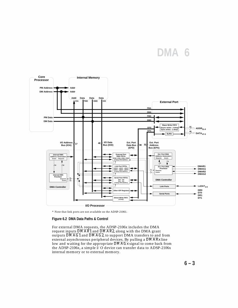
6DMA
6 – 3
For external DMA requests, the ADSP-2106x includes the DMArequest inputs DMAR1 and DMAR2, along with the DMA grantoutputs DMAG1 and DMAG2, to support DMA transfers to and fromexternal asynchronous peripheral devices. By pulling a DMARx linelow and waiting for the appropriate DMAGx signal to come back fromthe ADSP-2106x, a simple I/O device can transfer data to ADSP-2106xinternal memory or to external memory.
Ext. Port Data Bus
(EPD)
Slave Write FIFO(Async writes - 4 deep)(Sync writes - 2 deep)
Buffer
32
48
ADDR31-0
DATA47-0
External Port
Ext. Port Address
Bus (EPA)48 32
Data Data Data
PM Data
DM Data
48
PM Address
DM Address
Addr
Addr
I/O Data Bus (IOD)
Addr
17I/O Address Bus (IOA)
PMD
Core Processor
Internal Memory
IODIOA DMD
PMA
DMA
PMD
DMD
EPD
EPA
External PortDMA FIFOs
EPB0 EPB1 EPB2 EPB3(6-deep FIFO Buffers)
Other IOP Registers
Direct Write FIFO(6 deep)
Ext. Port DMAAddress Generators
Requests Grants
Ext. Port DMAPrioritizer
RequestsGrants
44
DMA Controller
DMAR1DMAG14
4 DMAR2DMAG2
Link Port FIFOsLBUF0 LBUF2 LBUF4LBUF1 LBUF3 LBUF5(2-deep FIFO Buffers)
Serial Port FIFOsRX0 TX0RX1 TX1
(2-deep FIFO Buffers)
LxDAT3-0
DR0DT0DR1DT1
10
10
DMA Controller
Internal DMAAddress Generators
Grants Requests
Internal DMAPrioritizer
RequestsGrants
10 10
Link Ports
Serial Ports
I/O Processor
* Note that link ports are not available on the ADSP-21061.
Figure 6.2 DMA Data Paths & Control

6 DMA
6 – 4
The ten DMA channels of the ADSP-21060 and ADSP-21062 arenumbered as shown in Table 6.1a, which also shows the correspondingdata buffer used with each channel.
DMA DataChannel# Buffer DescriptionDMA Channel 0 RX0 Serial Port 0 ReceiveDMA Channel 1 RX1 (or LBUF0) Serial Port 1 Receive (or Link Buffer 0)DMA Channel 2 TX0 Serial Port 0 TransmitDMA Channel 3 TX1 (or LBUF1) Serial Port 1 Transmit (or Link Buffer 1)DMA Channel 4 LBUF2 Link Buffer 2DMA Channel 5 LBUF3 Link Buffer 3DMA Channel 6 EPB0 (or LBUF4) Ext. Port FIFO Buffer 0 (or Link Buffer 4)DMA Channel 7* EPB1 (or LBUF5) Ext. Port FIFO Buffer 1 (or Link Buffer 5)DMA Channel 8* EPB2 Ext. Port FIFO Buffer 2DMA Channel 9 EPB3 Ext. Port FIFO Buffer 3
Table 6.1a ADSP-2106x DMA Channels & Data Buffers* DMAR1 and DMAG1 are handshake controls for DMA Channel 7.* DMAR2 and DMAG2 are handshake controls for DMA Channel 8.
The six DMA channels of the ADSP-21061 are numbered as shown inTable 6.1b, which also shows the corresponding data buffer used witheach channel.
DMA DataChannel# Buffer DescriptionDMA Channel 0 RX0 Serial Port 0 ReceiveDMA Channel 1 RX1 Serial Port 1 ReceiveDMA Channel 2 TX0 Serial Port 0 TransmitDMA Channel 3 TX1 Serial Port 1 TransmitDMA Channel 6* EPB0 Ext. Port FIFO Buffer 0DMA Channel 7* EPB1 Ext. Port FIFO Buffer 1
Table 6.1b ADSP-2106x DMA Channels & Data Buffers* DMAR2 and DMAG2 are handshake controls for DMA Channel 6.* DMAR1 and DMAG1 are handshake controls for DMA Channel 7.

6DMA
6 – 5
The following terms are used throughout this chapter, and are definedbelow for reference:
external port FIFO buffers EPB0, EPB1, EPB2, and EPB3—the IOPregisters used for external port DMAtransfers and single-word data transfers(from other ADSP-2106xs or from a hostprocessor); these buffers are 6-deep FIFOs
DMACx control registers the DMA control registers for the EPBxexternal port buffers: DMAC6, DMAC7,DMAC8, and DMAC9 (correspondingrespectively to EPB0, EPB1, EPB2, and EPB3)
DMA parameter registers the address (IIx), modifier (IMx), count (Cx),chain pointer (CPx), etc., registers used to setup a DMA transfer
transfer control block (TCB) a set of DMA parameter register valuesstored in memory that are downloaded bythe ADSP-2106x’s DMA controller forchained DMA operations
TCB chain loading the process in which the ADSP-2106x’s DMAcontroller downloads a TCB from memoryand autoinitializes the DMA parameterregisters
6.1.1 DMA Controller FeaturesThe ADSP-2106x’s DMA controller is designed to perform two basictypes of operations: external port block data transfers and I/O portdata transfers. The I/O ports on the ADSP-21060 and ADSP-21062 arethe link ports and serial ports. The I/O ports on the ADSP-21061 arethe serial ports.
External port block data transfers move data between ADSP-2106xinternal memory and external memory. The DMA controller must beprogrammed with the internal memory buffer size and address, theaddress increment, and the direction of transfer. Once setupprogramming is complete, DMA transfers begin automatically andcontinue until the entire buffer is transferred to or from internalmemory.
6 DMA
6 – 6
I/O port DMA transfers handle data transmitted and received throughthe ADSP-2106x’s serial ports and link ports. When performing I/ODMA, the same type of buffer is set up in internal memory, but insteadof accessing the external memory, the DMA controller accesses the I/Oport. The direction of data transfer is determined by the direction ofthe I/O port. When data is received at the port, it is automaticallytransferred to internal memory. Likewise, when the port needs totransmit a word, it is automatically fetched from internal memory.
An additional DMA capability allows the ADSP-2106x to support datatransfers between an external device and external memory. Thistransfer does not interfere with internal ADSP-2106x operations thatdo not use the external port.
External devices can participate in DMA transfers in two ways. Theexternal device can read or write to a DMA buffer on the ADSP-2106x,or it can assert a DMA Request input (DMARx) to request service.
In chained DMA operations, a DMA transfer can be programmed toautoinitialize another DMA operation upon completion.
6.1.2 Setting Up DMA TransfersDMA operations can be programmed by the ADSP-2106x coreprocessor, by an external host processor, or by the (external)ADSP-2106x bus master. The operation is programmed by writing tothe memory-mapped DMA control registers and parameter registers.A DMA channel is set up by writing a set of memory bufferparameters to the DMA parameter registers. The II, IM, and C registersmust be loaded with a starting address for the buffer, an addressmodifier, and a word count, respectively.
The external ports, link ports, and serial ports each have a DMA enablebit (DEN) in their main control register. Once a DMA channel is set upand enabled, data words received are automatically transferred to thebuffer in internal memory. Likewise, when the ADSP-2106x is ready totransmit data, a word is automatically transferred from internalmemory to the DMA buffer register. These transfers continue until theentire data buffer is received or transmitted.
DMA interrupts can be generated when an entire block of data hasbeen transferred. This occurs when the DMA channel’s count register(C) has decremented to zero (or EC register, in master mode only).
6DMA
6 – 7
DMA interrupts are latched and masked in the IRPTL and IMASKregisters, respectively; these registers are located in the ADSP-2106xprocessor core, not in the memory-mapped IOP register space.
TO START A NEW DMA SEQUENCE AFTER THE CURRENT ONE IS FINISHED,YOUR PROGRAM MUST FIRST CLEAR THE DMA ENABLE BIT, WRITE NEWPARAMETERS TO THE II, IM, AND C REGISTERS, AND THEN SET THE DMAENABLE BIT TO RE-ENABLE DMA.
(For chained DMA operations, however, this is not necessary; see“DMA Chaining.”)
For further details, see the “DMA Controller Operation,” “DMAChannel Parameter Registers,” and “DMA Interrupts” sections of thischapter.
6.2 DMA CONTROL REGISTERSThe registers used to control and configure DMA operations are part ofthe memory-mapped IOP register set. These registers are accessed bywriting to or (reading from) the appropriate address in memory.
Succeeding sections of this chapter describe the different operatingmodes of the DMA controller together with the associated controlregisters and bits. For complete information about the IOP registers,see the Control/Status Registers appendix of this manual.
The DMA control registers and data buffer registers are listed inTable 6.2. Note that the serial port and link port DMA control bits arelocated in the SPORT and link port control registers, not listed inTable 6.2—these control bits are described below under “Serial PortDMA Control” and “Link Port DMA Control.”
Two-dimensional DMA mode is enabled by the L2DDMA bit in theLCOM control register and the D2DMA bit in the SRCTL0 and SRCTL1registers. These bits should be cleared (to 0) for standard DMAoperations. Note that references to two-dimensional DMA are notapplicable to the ADSP-21061.

6 DMA
6 – 8
Register Name(s) Width DescriptionEPB0 48 External Port FIFO Buffer 0EPB1 48 External Port FIFO Buffer 1EPB2 48 External Port FIFO Buffer 2EPB3 48 External Port FIFO Buffer 3DMAC6 16 DMA Channel 6 Control Register
(Ext. Port Buffer 0 or Link Buffer 4)1, 2
DMAC7 16 DMA Channel 7 Control Register (Ext. Port Buffer 1 orLink Buffer 5)1, 2
DMAC8 16 DMA Channel 8 Control Register (Ext. Port Buffer 2)3
DMAC9 16 DMA Channel 9 Control Register (Ext. Port Buffer 3)3
DMASTAT 32 DMA Channel Status RegisterII0, IM0, C0, CP0 16-18 DMA Channel 0 Parameter Registers (SPORT0 Receive)4
GP0, DB0, DA0II1, IM1, C1, CP1 16-18 DMA Channel 1 Parameter Registers (SPORT1 Receive orGP1, DB1, DA1 Link Buffer 0)1, 2, 4, 5
II2, IM2, C2, CP2 16-18 DMA Channel 2 Parameter Registers (SPORT0 Transmit)4, 5
GP2, DB2, DA2II3, IM3, C3, CP3 16-18 DMA Channel 3 Parameter Registers (SPORT1 Transmit orGP3, DB3, DA3 Link Buffer 1)1, 2, 4, 5
II4, IM4, C4, CP4 16-18 DMA Channel 4 Parameter Registers (Link Buffer 2)1, 5
GP4, DB4, DA4II5, IM5, C5, CP5 16-18 DMA Channel 5 Parameter Registers (Link Buffer 3)1, 5
GP5, DB5, DA5II6, IM6, C6, CP6 16-32 DMA Channel 6 Parameter Registers (Ext. Port Buffer 0 orGP6, EI6, EM6, EC6 Link Buffer 4)1, 2
II7, IM7, C7, CP7 16-32 DMA Channel 7 Parameter Registers (Ext. Port Buffer 1 orGP7, EI7, EM7, EC7 Link Buffer 5)1, 2
II8, IM8, C8, CP8 16-32 DMA Channel 8 Parameter Registers (Ext. Port Buffer 2)3
GP8, EI8, EM8, EC8II9, IM9, C9, CP9 16-32 DMA Channel 9 Parameter Registers (Ext. Port Buffer 3)3
GP9, EI9, EM9, EC9
Table 6.2 DMA Control, Buffer, & Parameter Registers
1. DMA control, buffer, and parameter registers associated with the link ports are notapplicable to the ADSP-21061.
2. There are no shared DMA channels on the ADPS-21061.3. DMA control, buffer, and parameter registers associated wiht DMA channels 8 and 9 are
not applicalbe to the ADSP-21061.4. The IM0, IM1, IM2, and IM3 registers contain the fixed value of 1 on the ADSP-21061.5. The DBx and DAx registers are not available on the ADSP-21061 because there is no 2-D
DMA on the ADSP-21061.
6DMA
6 – 9
11 10 9 8 7 6 5 4 3 2 1 0
000000000000
15 14 13 12
0000
DENDMA Enable for Ext. Port1=enable, 0=disable
CHENDMA Chaining Enable for Ext. Port1=enable, 0=disable
TRANDMA Channel Direction0=read from ext. memory1=write to ext. memory
PSPacking Status (read-only)00=packing complete01=1st stage of all pack & unpack modes10=2nd stage of 16-to-48 bit pack/unpack,
or 2nd stage of 32-to-48 pack/unpack
FLSHFlush Ext. Port FIFO Buffer
1=flush
EXTERNExt. Devices to Ext. Memory DMA
1=extern mode
FSExt. Port FIFO Buffer Status
00=empty, 10=partially full, 11=full
26 25 24 23 22 21 20 19 18 17
000000000000
31 30 29 28 27
0000
16
DTYPEData Type0=data, 1=instructions
PMODEPacking Mode00=no packing01=16/3210=16/4811=32/48
INTIOSingle-Word Interrupts for
Ext. Port FIFO Buffers1=enable, 0=disable
HSHAKEDMA Handshake
1=enable, 0=disable
MASTERDMA Master Mode
1=enable, 0=disable
MSWFMost Significant Word First
for Packing1=enable, 0=disable
Figure 6.3 DMACx Registers
6.2.1 External Port DMA Control RegistersEach external port DMA channel has its own control register. The registersare named DMAC6, DMAC7, DMAC8, and DMAC9, corresponding tochannels 6-9. Note that for the ADSP-21061 only DMA channels 6 and 7 ofthe external port are applicable. Table 6.3 shows the contents of theDMACx registers. All bits are active high unless stated otherwise.
The control bits in the DMACx registers take effect during the secondcycle after the write to the register is completed. The exception to this ruleis the FLSH bit, which takes effect in the third cycle after the write.
To start a new DMA sequence after the current one is finished, yourprogram must first clear the DEN enable bit, write new parameters to theII, IM, and C registers, and then set the DEN bit to re-enable DMA. (For
6 DMA
6 – 10
chained DMA operations, however, this is not necessary.)
Bit(s) Name Definition0 DEN DMA Enable for External Port1 CHEN DMA Chaining Enable for External Port2 TRAN Transmit/Receive (1=transmit, 0=receive)3-4 PS Pack Status (read-only)5 DTYPE Data Type (0=data, 1=instructions)6-7 PMODE Packing Mode (00=none, 01=16/32, 10=16/48, 11=32/48)8 MSWF Most Significant Word First during packing9 MASTER Master Mode Enable10 HSHAKE Handshake Mode Enable (DMARx, DMAGx)11 INTIO Single-Word Interrupt Enable for external port buffers12 EXTERN External Handshake Mode Enable13 FLSH Flush DMA Buffers & Status14-15 FS External port buffer status (00=empty, 11=full,
10=partially full)16-31 reserved
Table 6.3 External Port DMA Control Registers (DMACx)
The control and status bits in the DMACx registers are furtherdescribed below:
DEN Enables DMA for the external port buffers. (Note that the DMAchannels shared between the external port and link ports,channels 6 and 7, may also become enabled by the link buffers; seethe “Selection Of Shared DMA Channels” section of this chapter.Also note that for the ADSP-21061 there are no shared DMAchannels.)
CHEN Enables chained DMA transfers. When CHEN=1 and DEN=0, theDMA channel is placed in chain insertion mode in which a newDMA chain can be inserted into the current chain withoutaffecting the current DMA transfer. This mode of operation isidentical to CHEN=1 and DEN=1 except that automatic chainingis disabled when the current DMA transfer ends. The complete listof modes selected by the CHEN and DEN bits are as follows:
CHEN DEN Mode of Operation0 0 Chaining disabled, DMA disabled0 1 Chaining disabled, DMA enabled1 0 Chain Insertion mode (chaining enabled, DMA
enabled, auto-chaining disabled)1 1 Chaining enabled, DMA enabled, auto-chaining
enabled

6DMA
6 – 11
TRAN Transmit (1) or Receive (0). (1=read from ADSP-2106x, 0=write toADSP-2106x.) This bit specifies the data transfer direction asinternal-to-external when set to 1. (When EXTERN=1, settingTRAN=1 specifies a read from external memory and TRAN=0specifies a write to external memory.)
PS PS is a two-bit status field that indicates whether the packingbuffer is on its first, second, or last pack:
PS Status00 pack complete01 1st stage of all pack and unpack modes10 2nd stage of 16-to-48 bit pack or unpack modes,
or 2nd stage of 32-to-48 bit pack or unpack modes11 reserved
DTYPE Specifies the type of data being transferred; this information isused by internal memory to determine the word width. DTYPE=1overrides the IMDW bits and forces a 48-bit (3-column) memorytransfer. DTYPE=0 defers to the data word setting of the IMDWbits in the SYSCON register. The data word may be 32-bit or 40-bit, as determined by the setting of the IMDW bits in the SYSCONregister.
PMODE PMODE is a two-bit value specifying the EPBx buffer packingmode. For host processor accesses of the EPBx buffers, the HPMbits of the SYSCON register must be set to correspond to theexternal bus width specified by PMODE.
PMODE Packing Mode00 No packing/unpacking01 16-bit external bus to/from 32-bit internal packing10 16-bit external bus to/from 48-bit internal packing11 32-bit external bus to/from 48-bit internal packing
MSWF Specifies the order in which words are packed, for 16-to-32 bitpacking and 16-to-48 bit packing. MSWF is ignored for 32-to-48 bitpacking. When MSWF=1, packing is done MSW first (mostsignificant 16-bit word first). When MSWF=0, packing is doneLSW first.
INTIO Used when DEN=0, to allow the external port DMA interrupts tooccur for individual words received and transmitted. GeneratingDMA interrupts in this fashion is useful for implementinginterrupt-driven single-word transfers under control of the ADSP-2106x core processor. Setting INTIO=1 causes the interrupts tooccur when an EPBx input buffer is “not empty” (for TRAN=0) orwhen an output buffer is “not full” (for TRAN=1).
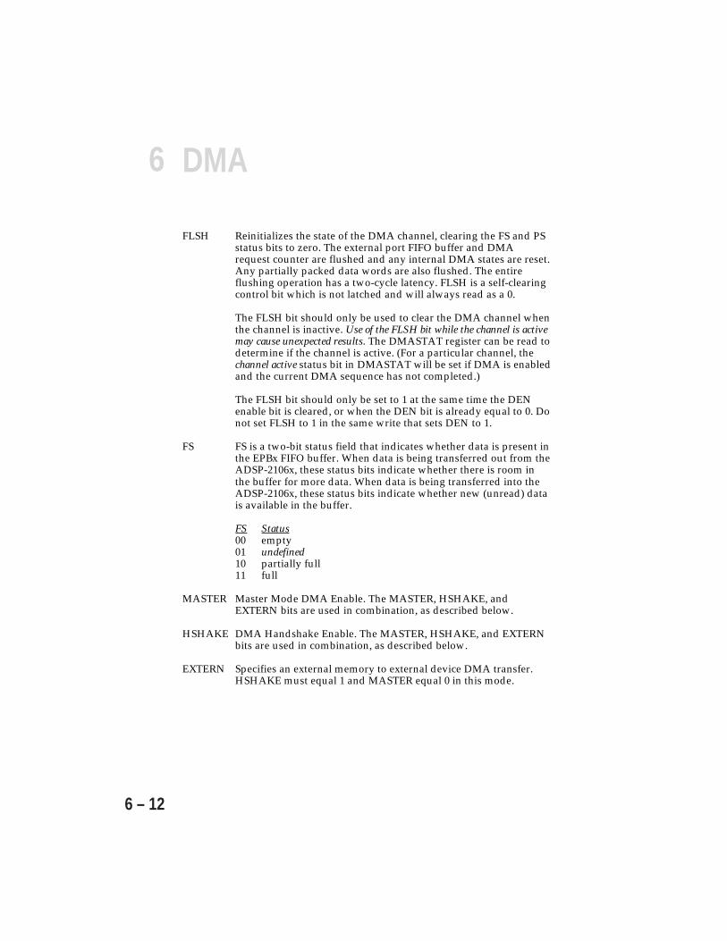
6 DMA
6 – 12
FLSH Reinitializes the state of the DMA channel, clearing the FS and PSstatus bits to zero. The external port FIFO buffer and DMArequest counter are flushed and any internal DMA states are reset.Any partially packed data words are also flushed. The entireflushing operation has a two-cycle latency. FLSH is a self-clearingcontrol bit which is not latched and will always read as a 0.
The FLSH bit should only be used to clear the DMA channel whenthe channel is inactive. Use of the FLSH bit while the channel is activemay cause unexpected results. The DMASTAT register can be read todetermine if the channel is active. (For a particular channel, thechannel active status bit in DMASTAT will be set if DMA is enabledand the current DMA sequence has not completed.)
The FLSH bit should only be set to 1 at the same time the DENenable bit is cleared, or when the DEN bit is already equal to 0. Donot set FLSH to 1 in the same write that sets DEN to 1.
FS FS is a two-bit status field that indicates whether data is present inthe EPBx FIFO buffer. When data is being transferred out from theADSP-2106x, these status bits indicate whether there is room inthe buffer for more data. When data is being transferred into theADSP-2106x, these status bits indicate whether new (unread) datais available in the buffer.
FS Status00 empty01 undefined10 partially full11 full
MASTER Master Mode DMA Enable. The MASTER, HSHAKE, andEXTERN bits are used in combination, as described below.
HSHAKE DMA Handshake Enable. The MASTER, HSHAKE, and EXTERNbits are used in combination, as described below.
EXTERN Specifies an external memory to external device DMA transfer.HSHAKE must equal 1 and MASTER equal 0 in this mode.
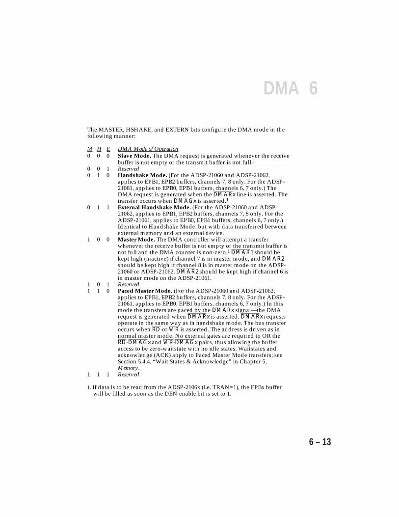
6DMA
6 – 13
The MASTER, HSHAKE, and EXTERN bits configure the DMA mode in thefollowing manner:
M H E DMA Mode of Operation0 0 0 Slave Mode. The DMA request is generated whenever the receive
buffer is not empty or the transmit buffer is not full.10 0 1 Reserved0 1 0 Handshake Mode. (For the ADSP-21060 and ADSP-21062,
applies to EPB1, EPB2 buffers, channels 7, 8 only. For the ADSP-21061, applies to EPB0, EPB1 buffers, channels 6, 7 only.) TheDMA request is generated when the DMARx line is asserted. Thetransfer occurs when DMAGx is asserted.1
0 1 1 External Handshake Mode. (For the ADSP-21060 and ADSP-21062, applies to EPB1, EPB2 buffers, channels 7, 8 only. For theADSP-21061, applies to EPB0, EPB1 buffers, channels 6, 7 only.)Identical to Handshake Mode, but with data transferred betweenexternal memory and an external device.
1 0 0 Master Mode. The DMA controller will attempt a transferwhenever the receive buffer is not empty or the transmit buffer isnot full and the DMA counter is non-zero.1 DMAR1 should bekept high (inactive) if channel 7 is in master mode, and DMAR2should be kept high if channel 8 is in master mode on the ADSP-21060 or ADSP-21062. DMAR2 should be kept high if channel 6 isin master mode on the ADSP-21061.
1 0 1 Reserved1 1 0 Paced Master Mode. (For the ADSP-21060 and ADSP-21062,
applies to EPB1, EPB2 buffers, channels 7, 8 only. For the ADSP-21061, applies to EPB0, EPB1 buffers, channels 6, 7 only.) In thismode the transfers are paced by the DMARx signal—the DMArequest is generated when DMARx is asserted. DMARx requestsoperate in the same way as in handshake mode. The bus transferoccurs when RD or WR is asserted. The address is driven as innormal master mode. No external gates are required to OR theRD-DMAGx and WR-DMAGx pairs, thus allowing the bufferaccess to be zero-waitstate with no idle states. Waitstates andacknowledge (ACK) apply to Paced Master Mode transfers; seeSection 5.4.4, “Wait States & Acknowledge” in Chapter 5,Memory.
1 1 1 Reserved
1. If data is to be read from the ADSP-2106x (i.e. TRAN=1), the EPBx bufferwill be filled as soon as the DEN enable bit is set to 1.
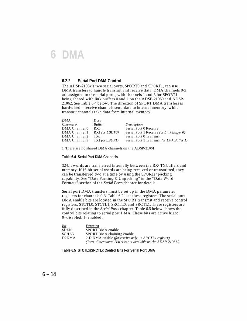
6 DMA
6 – 14
6.2.2 Serial Port DMA ControlThe ADSP-2106x’s two serial ports, SPORT0 and SPORT1, can useDMA transfers to handle transmit and receive data. DMA channels 0-3are assigned to the serial ports, with channels 1 and 3 for SPORT1being shared with link buffers 0 and 1 on the ADSP-21060 and ADSP-21062. See Table 6.4 below. The direction of SPORT DMA transfers ishardwired—receive channels send data to internal memory, whiletransmit channels take data from internal memory.
DMA DataChannel # Buffer DescriptionDMA Channel 0 RX0 Serial Port 0 ReceiveDMA Channel 1 RX1 (or LBUF0) Serial Port 1 Receive (or Link Buffer 0)1
DMA Channel 2 TX0 Serial Port 0 TransmitDMA Channel 3 TX1 (or LBUF1) Serial Port 1 Transmit (or Link Buffer 1)1
1. There are no shared DMA channels on the ADSP-21061.
Table 6.4 Serial Port DMA Channels
32-bit words are transferred internally between the RX/TX buffers andmemory. If 16-bit serial words are being received or transmitted, theycan be transferred two at a time by using the SPORTs’ packingcapability. See “Data Packing & Unpacking” in the “Data WordFormats” section of the Serial Ports chapter for details.
Serial port DMA transfers must be set up in the DMA parameterregisters for channels 0-3. Table 6.2 lists these registers. The serial portDMA enable bits are located in the SPORT transmit and receive controlregisters, STCTL0, STCTL1, SRCTL0, and SRCTL1. These registers arefully described in the Serial Ports chapter. Table 6.5 below shows thecontrol bits relating to serial port DMA. These bits are active high:0=disabled, 1=enabled.
Bit FunctionSDEN SPORT DMA enableSCHEN SPORT DMA chaining enableD2DMA 2-D DMA enable (for receive only, in SRCTLx register)
(Two -dimensional DMA is not available on the ADSP-21061.)
Table 6.5 STCTLx/SRCTLx Control Bits For Serial Port DMA
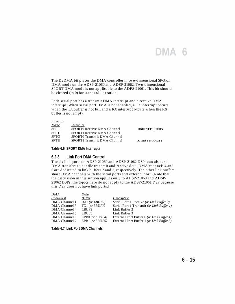
6DMA
6 – 15
The D2DMA bit places the DMA controller in two-dimensional SPORTDMA mode on the ADSP-21060 and ADSP-21062. Two-dimensionalSPORT DMA mode is not applicable to the ADPS-21061. This bit shouldbe cleared (to 0) for standard operation.
Each serial port has a transmit DMA interrupt and a receive DMAinterrupt. When serial port DMA is not enabled, a TX interrupt occurswhen the TX buffer is not full and a RX interrupt occurs when the RXbuffer is not empty.
InterruptName InterruptSPR0I SPORT0 Receive DMA Channel HIGHEST PRIORITYSPR1I SPORT1 Receive DMA ChannelSPT0I SPORT0 Transmit DMA ChannelSPT1I SPORT1 Transmit DMA Channel LOWEST PRIORITY
Table 6.6 SPORT DMA Interrupts
6.2.3 Link Port DMA ControlThe six link ports on ADSP-21060 and ADSP-21062 DSPs can also useDMA transfers to handle transmit and receive data. DMA channels 4 and5 are dedicated to link buffers 2 and 3, respectively. The other link buffersshare DMA channels with the serial ports and external port. [Note thatthe discussion in this section applies only to ADSP-21060 and ADSP-21062 DSPs; the topics here do not apply to the ADSP-21061 DSP becausethis DSP does not have link ports.]
DMA DataChannel # Buffer DescriptionDMA Channel 1 RX1 (or LBUF0) Serial Port 1 Receive (or Link Buffer 0)DMA Channel 3 TX1 (or LBUF1) Serial Port 1 Transmit (or Link Buffer 1)DMA Channel 4 LBUF2 Link Buffer 2DMA Channel 5 LBUF3 Link Buffer 3DMA Channel 6 EPB0 (or LBUF4) External Port Buffer 0 (or Link Buffer 4)DMA Channel 7 EPB1 (or LBUF5) External Port Buffer 1 (or Link Buffer 5)
Table 6.7 Link Port DMA Channels
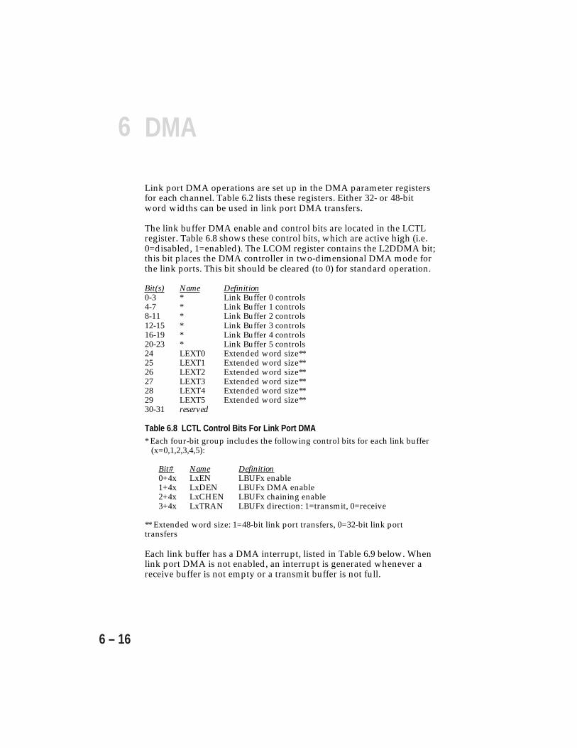
6 DMA
6 – 16
Link port DMA operations are set up in the DMA parameter registersfor each channel. Table 6.2 lists these registers. Either 32- or 48-bitword widths can be used in link port DMA transfers.
The link buffer DMA enable and control bits are located in the LCTLregister. Table 6.8 shows these control bits, which are active high (i.e.0=disabled, 1=enabled). The LCOM register contains the L2DDMA bit;this bit places the DMA controller in two-dimensional DMA mode forthe link ports. This bit should be cleared (to 0) for standard operation.
Bit(s) Name Definition0-3 * Link Buffer 0 controls4-7 * Link Buffer 1 controls8-11 * Link Buffer 2 controls12-15 * Link Buffer 3 controls16-19 * Link Buffer 4 controls20-23 * Link Buffer 5 controls24 LEXT0 Extended word size**25 LEXT1 Extended word size**26 LEXT2 Extended word size**27 LEXT3 Extended word size**28 LEXT4 Extended word size**29 LEXT5 Extended word size**30-31 reserved
Table 6.8 LCTL Control Bits For Link Port DMA* Each four-bit group includes the following control bits for each link buffer (x=0,1,2,3,4,5):
Bit# Name Definition0+4x LxEN LBUFx enable1+4x LxDEN LBUFx DMA enable2+4x LxCHEN LBUFx chaining enable3+4x LxTRAN LBUFx direction: 1=transmit, 0=receive
** Extended word size: 1=48-bit link port transfers, 0=32-bit link porttransfers
Each link buffer has a DMA interrupt, listed in Table 6.9 below. Whenlink port DMA is not enabled, an interrupt is generated whenever areceive buffer is not empty or a transmit buffer is not full.
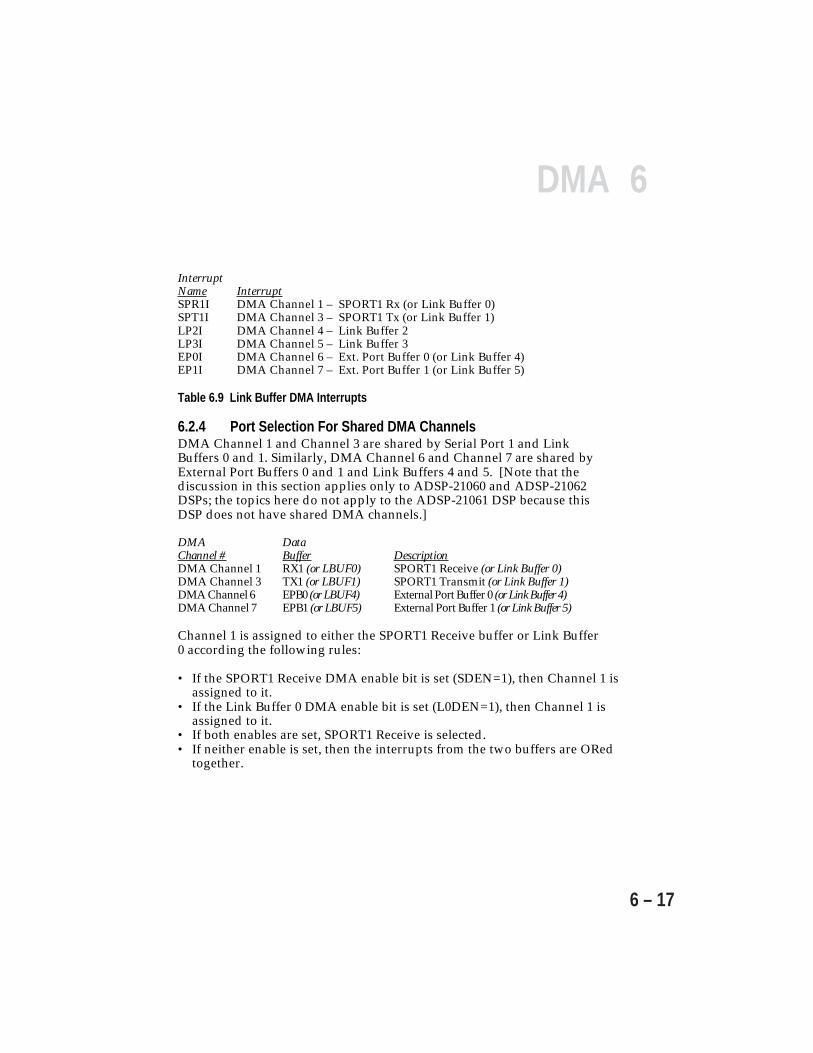
6DMA
6 – 17
InterruptName InterruptSPR1I DMA Channel 1 – SPORT1 Rx (or Link Buffer 0)SPT1I DMA Channel 3 – SPORT1 Tx (or Link Buffer 1)LP2I DMA Channel 4 – Link Buffer 2LP3I DMA Channel 5 – Link Buffer 3EP0I DMA Channel 6 – Ext. Port Buffer 0 (or Link Buffer 4)EP1I DMA Channel 7 – Ext. Port Buffer 1 (or Link Buffer 5)
Table 6.9 Link Buffer DMA Interrupts
6.2.4 Port Selection For Shared DMA ChannelsDMA Channel 1 and Channel 3 are shared by Serial Port 1 and LinkBuffers 0 and 1. Similarly, DMA Channel 6 and Channel 7 are shared byExternal Port Buffers 0 and 1 and Link Buffers 4 and 5. [Note that thediscussion in this section applies only to ADSP-21060 and ADSP-21062DSPs; the topics here do not apply to the ADSP-21061 DSP because thisDSP does not have shared DMA channels.]
DMA DataChannel # Buffer DescriptionDMA Channel 1 RX1 (or LBUF0) SPORT1 Receive (or Link Buffer 0)DMA Channel 3 TX1 (or LBUF1) SPORT1 Transmit (or Link Buffer 1)DMA Channel 6 EPB0 (or LBUF4) External Port Buffer 0 (or Link Buffer 4)DMA Channel 7 EPB1 (or LBUF5) External Port Buffer 1 (or Link Buffer 5)
Channel 1 is assigned to either the SPORT1 Receive buffer or Link Buffer0 according the following rules:
• If the SPORT1 Receive DMA enable bit is set (SDEN=1), then Channel 1 isassigned to it.
• If the Link Buffer 0 DMA enable bit is set (L0DEN=1), then Channel 1 isassigned to it.
• If both enables are set, SPORT1 Receive is selected.• If neither enable is set, then the interrupts from the two buffers are ORed
together.
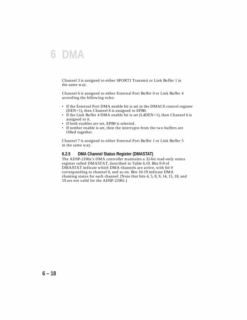
6 DMA
6 – 18
Channel 3 is assigned to either SPORT1 Transmit or Link Buffer 1 inthe same way.
Channel 6 is assigned to either External Port Buffer 0 or Link Buffer 4according the following rules:
• If the External Port DMA enable bit is set in the DMAC6 control register(DEN=1), then Channel 6 is assigned to EPB0.
• If the Link Buffer 4 DMA enable bit is set (L4DEN=1), then Channel 6 isassigned to it.
• If both enables are set, EPB0 is selected.• If neither enable is set, then the interrupts from the two buffers are
ORed together.
Channel 7 is assigned to either External Port Buffer 1 or Link Buffer 5in the same way.
6.2.5 DMA Channel Status Register (DMASTAT)The ADSP-2106x’s DMA controller maintains a 32-bit read-only statusregister called DMASTAT, described in Table 6.10. Bits 0-9 ofDMASTAT indicate which DMA channels are active, with bit 0corresponding to channel 0, and so on. Bits 10-19 indicate DMAchaining status for each channel. [Note that bits 4, 5, 8, 9, 14, 15, 18, and19 are not valid for the ADSP-21061.]
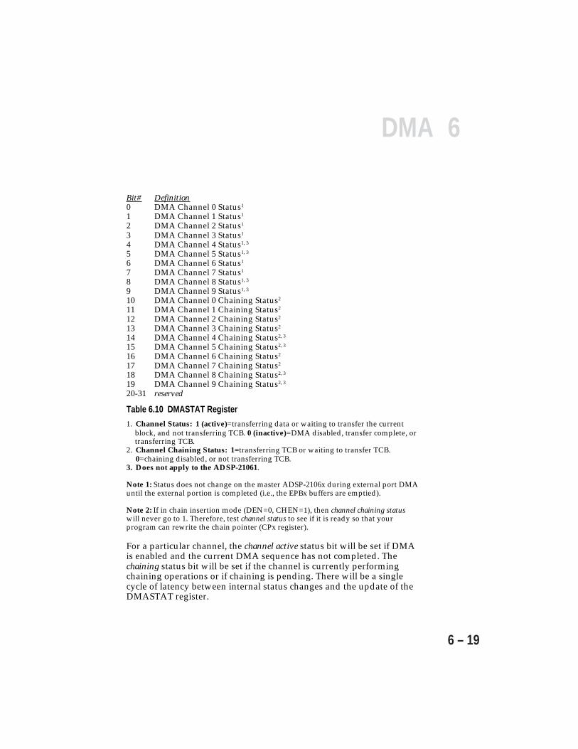
6DMA
6 – 19
Bit# Definition0 DMA Channel 0 Status1
1 DMA Channel 1 Status1
2 DMA Channel 2 Status1
3 DMA Channel 3 Status1
4 DMA Channel 4 Status1, 3
5 DMA Channel 5 Status1, 3
6 DMA Channel 6 Status1
7 DMA Channel 7 Status1
8 DMA Channel 8 Status1, 3
9 DMA Channel 9 Status1, 3
10 DMA Channel 0 Chaining Status2
11 DMA Channel 1 Chaining Status2
12 DMA Channel 2 Chaining Status2
13 DMA Channel 3 Chaining Status2
14 DMA Channel 4 Chaining Status2, 3
15 DMA Channel 5 Chaining Status2, 3
16 DMA Channel 6 Chaining Status2
17 DMA Channel 7 Chaining Status2
18 DMA Channel 8 Chaining Status2, 3
19 DMA Channel 9 Chaining Status2, 3
20-31 reserved
Table 6.10 DMASTAT Register
1. Channel Status: 1 (active)=transferring data or waiting to transfer the currentblock, and not transferring TCB. 0 (inactive)=DMA disabled, transfer complete, ortransferring TCB.
2. Channel Chaining Status: 1=transferring TCB or waiting to transfer TCB.0=chaining disabled, or not transferring TCB.
3. Does not apply to the ADSP-21061.
Note 1: Status does not change on the master ADSP-2106x during external port DMAuntil the external portion is completed (i.e., the EPBx buffers are emptied).
Note 2: If in chain insertion mode (DEN=0, CHEN=1), then channel chaining statuswill never go to 1. Therefore, test channel status to see if it is ready so that yourprogram can rewrite the chain pointer (CPx register).
For a particular channel, the channel active status bit will be set if DMAis enabled and the current DMA sequence has not completed. Thechaining status bit will be set if the channel is currently performingchaining operations or if chaining is pending. There will be a singlecycle of latency between internal status changes and the update of theDMASTAT register.

6 DMA
6 – 20
As an alternative to interrupt-driven DMA, polling DMASTAT can beused to determine when a single DMA sequence has completed:
1. Read DMASTAT.2. If both status bits for the channel are inactive, the DMA sequence
has completed.
If chaining is enabled, however, polling should not be used since thenext DMA sequence may be under way by the time the polled status isreturned.
6.3 DMA CONTROLLER OPERATIONThe following sections discuss the operation of the ADSP-2106x’sDMA controller and describe how DMA transfers occur.
In the ADSP-2106x, the DMA controller operations are centered on theinternal I/O bus. The serial ports, link ports, and external port areconnected to the internal memory via the I/O Data bus (IOD), and theDMA controller generates internal memory addresses on the I/OAddress bus (IOA).
The DMA controller maintains 10 DMA channels that are used by theexternal port, the link ports, and the serial ports. A DMA channelconsists of a set of parameter registers which specify a data buffer ininternal memory, plus the hardware required by an I/O port torequest DMA service.
To transfer data, the DMA controller accepts internal requests fromI/O ports and sends back an internal grant when they are serviced.The DMA controller contains priority logic to determine whichchannel can drive the bus in any given cycle. The DMA transfer neverconflicts with the core for internal memory accesses because theinternal memory has separate ports for core and I/O accesses.
Each external port DMA channel has a control/status register which isused to set the operating mode of the channel and to return statusinformation. All of the DMA control and parameter registers areaccessible to external devices. This allows a host, or another ADSP-2106x, to set up a DMA channel and initiate transfers without localADSP-2106x involvement. The local ADSP-2106x can set up a DMA
6DMA
6 – 21
channel on itself by writing to its DMA control and parameterregisters.
The external port and link port DMA channels can be configured totransmit or receive data from internal memory. The serial port DMAchannels, however, are unidirectional, either transmit or receive only.
6.3.1 DMA Channel Parameter RegistersThe DMA channels operate in a similar fashion as the ADSP-2106x’sData Address Generators (DAGs). Each channel has of a set ofparameter registers including an index register (IIx) and modifyregister (IMx) which are used to set up a data buffer in internalmemory. The index register must be initialized with a starting addressfor the data buffer. The address in the index register is output onto theADSP-2106x’s IOA (I/O Address) bus and applied to internal memoryduring each DMA cycle. (A DMA cycle is defined as a clock cycle inwhich a DMA transfer is taking place.)
All addresses in the 17-bit index registers are offset by 0x0002 0000, thefirst internal RAM location, before they are used by the DMAcontroller. Since the index registers are only 17 bits wide, DMAtransfers cannot be made to short word address space. (16-bit shortword data can be transferred within 32-bit words, however, using thepacking capability of the external port and serial port DMA channels.)
After each data word is transferred to or from internal memory, theDMA controller adds the modify value to the index register to generatethe address for the next DMA transfer; the modify value is added tothe index value and written back into the index register. The modifyvalue in the IM register is a signed integer, to allow both incrementingand decrementing. Note that if the index register is modified past itsmaximum 17-bit value (i.e. out of the address range of internalmemory), it will wraparound to zero (offset by 0x0002 0000). Themodify value for DMA channels 0-3 is fixed to 1 on the ADSP-21061;this DSP does not have the IM0-3 registers.
Each DMA channel has a count register (Cx) which must be initializedwith a word count to be transferred. The count register is decrementedafter each DMA transfer on that channel; when the count reaches zero,the interrupt for that channel can be generated.
Caution: If the count register is initialized with zero, DMA transfers on

6 DMA
6 – 22
that channel are not disabled. Rather, 216 transfers will be performed.This occurs because the first transfer is started before the count value istested. The correct way to disable a DMA channel is to clear its DMAenable bit in the corresponding control register.
To start a new DMA sequence after the current one is finished, your programmust first clear the DEN enable bit, write new parameters to the II, IM, and Cregisters, and then set the DEN bit to re-enable DMA.
(For chained DMA operations, however, this is not necessary.)
Each DMA channel also has a chain pointer register (CPx) and ageneral-purpose register (GPx). The CP register is used in chainedDMA operations (as described below in “DMA Chaining”), and theGP register can be used for any purpose.
The external port DMA channels each contain three additionalparameter registers, the external index register (EIx), external modifyregister (EMx), and external count register (ECx). (These registers arenot included in the serial port and link port DMA channels.) The EI,EM, and EC registers are used to generate 32-bit addresses driven outof the external port, for master mode DMA transfers between internalmemory and external memory or devices. Master mode is configuredby the MASTER bit of each DMACx control register. The EC registermust be loaded with the number of external bus transfers to occur (inmaster mode only). (Note: This differs from the number of wordstransferred by the DMA controller if word packing is used.) EIX maynot index internal memory. If DMA data is broadcast, write space datais not written to the internal memory of the broadcaster.
Instead of the EI, EM, and EC registers, the serial port and link portDMA channels have the DA and DB registers. These registers are usedfor two-dimensional array addressing in mesh multiprocessingapplications, but may also be used as general-purpose registers instandard, one-dimensional DMA operations.
Figure 6.4 shows a block diagram of the DMA controller’s addressgenerator. Table 6.11 defines the DMA parameter registers, andTable 6.12 lists the parameter registers for each DMA channel. Theparameter registers are uninitialized following a processor reset.
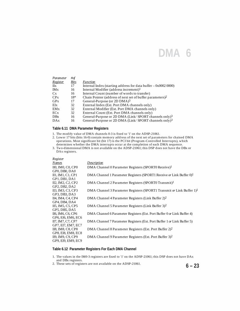
6DMA
6 – 23
Parameter #ofRegister Bits FunctionIIx 17 Internal Index (starting address for data buffer – 0x0002 0000)IMx 16 Internal Modifier (address increment)1Cx 16 Internal Count (number of words to transfer)CPx 18* Chain Pointer (address of next set of buffer parameters)2GPx 17 General-Purpose (or 2D DMA)3EIx 32 External Index (Ext. Port DMA channels only)EMx 32 External Modifier (Ext. Port DMA channels only)ECx 32 External Count (Ext. Port DMA channels only)DBx 16 General-Purpose or 2D DMA (Link/SPORT channels only)3
DAx 16 General-Purpose or 2D DMA (Link/SPORT channels only)3
Table 6.11 DMA Parameter Registers1. The modify value of DMA channels 0-3 is fixed to '1' on the ADSP-21061.2. Lower 17 bits (bits 16-0) contain memory address of the next set of parameters for chained DMA
operations. Most significant bit (bit 17) is the PCI bit (Program-Controlled Interrupts), whichdetermines whether the DMA interrupts occur at the completion of each DMA sequence.
3. Two-dimensional DMA is not available on the ADSP-21061; this DSP does not have the DBx orDAx registers.
RegisterNames DescriptionII0, IM0, C0, CP0 DMA Channel 0 Parameter Registers (SPORT0 Receive)1GP0, DB0, DA0II1, IM1, C1, CP1 DMA Channel 1 Parameter Registers (SPORT1 Receive or Link Buffer 0)1GP1, DB1, DA1II2, IM2, C2, CP2 DMA Channel 2 Parameter Registers (SPORT0 Transmit)1GP2, DB2, DA2II3, IM3, C3, CP3 DMA Channel 3 Parameter Registers (SPORT1 Transmit or Link Buffer 1)1GP3, DB3, DA3II4, IM4, C4, CP4 DMA Channel 4 Parameter Registers (Link Buffer 2)2GP4, DB4, DA4II5, IM5, C5, CP5 DMA Channel 5 Parameter Registers (Link Buffer 3)2GP5, DB5, DA5II6, IM6, C6, CP6 DMA Channel 6 Parameter Registers (Ext. Port Buffer 0 or Link Buffer 4)GP6, EI6, EM6, EC6II7, IM7, C7, CP7 DMA Channel 7 Parameter Registers (Ext. Port Buffer 1 or Link Buffer 5)GP7, EI7, EM7, EC7II8, IM8, C8, CP8 DMA Channel 8 Parameter Registers (Ext. Port Buffer 2)2GP8, EI8, EM8, EC8II9, IM9, C9, CP9 DMA Channel 9 Parameter Registers (Ext. Port Buffer 3)2GP9, EI9, EM9, EC9
Table 6.12 Parameter Registers For Each DMA Channel
1. The values in the IM0-3 registers are fixed to '1' on the ADSP-21061; this DSP does not have DAxand DBx registers.
2. These sets of registers are not available on the ADSP-21061.
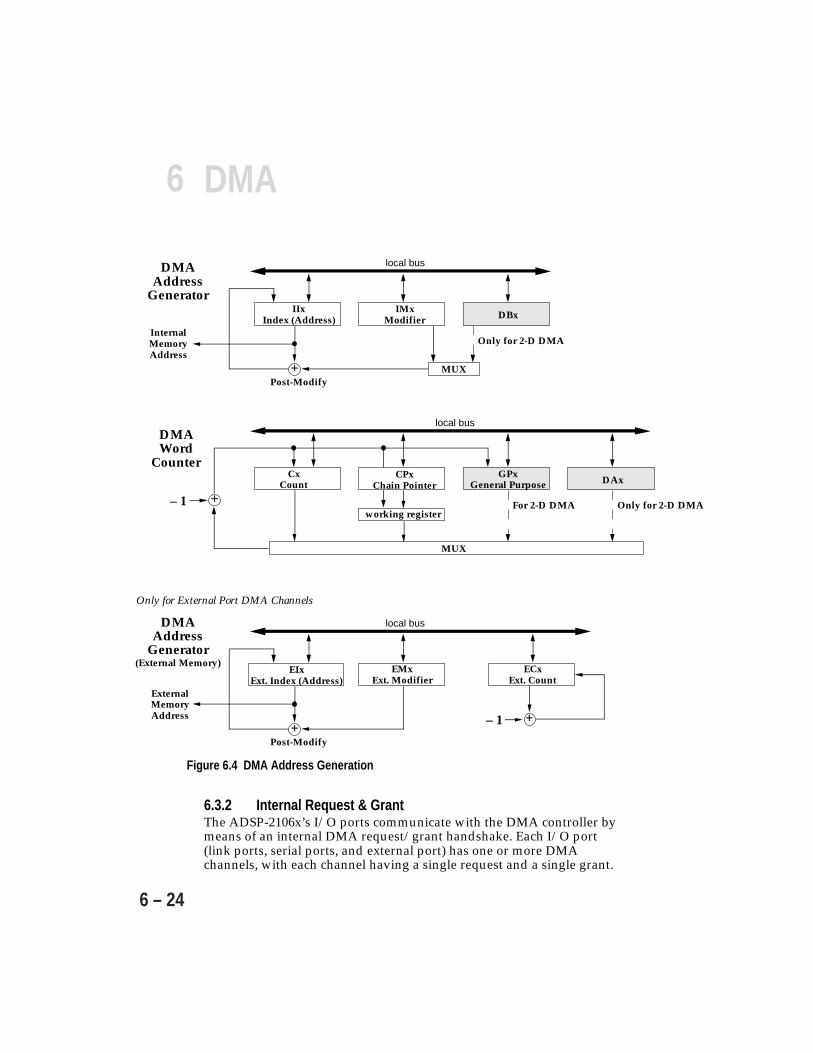
6 DMA
6 – 24
local bus
IMxModifier DBx
MUX
InternalMemoryAddress
DMA Address
Generator
Only for 2-D DMA
local bus
CxCount
CPxChain Pointer
GPxGeneral Purpose
MUX
DMA Word
Counter
– 1
DAx
For 2-D DMA Only for 2-D DMAworking register
local bus
EMxExt. Modifier
DMA Address
Generator(External Memory)
ECxExt. Count
+
+
Only for External Port DMA Channels
– 1
IIxIndex (Address)
+Post-Modify
ExternalMemoryAddress
+Post-Modify
EIxExt. Index (Address)
Figure 6.4 DMA Address Generation
6.3.2 Internal Request & GrantThe ADSP-2106x’s I/O ports communicate with the DMA controller bymeans of an internal DMA request/grant handshake. Each I/O port(link ports, serial ports, and external port) has one or more DMAchannels, with each channel having a single request and a single grant.
6DMA
6 – 25
When a particular I/O port needs to write data to internal memory, itasserts its request. This request is prioritized with all other valid DMArequests. See Figure 6.2.
When a channel becomes the highest priority requester, its internalgrant is asserted by the DMA controller. In the next clock cycle, theDMA transfer is started. When an I/O port wishes to read data frominternal memory, the sequence is the same.
If a DMA channel is disabled, no grants will be given for that channel,regardless of whether it has data to transfer.
6.3.3 DMA Channel PrioritizationSince more than one DMA channel may have a request active in aparticular cycle, a prioritization scheme is used to select the channel toservice. Prioritization is needed to determine which channel can usethe IOD (I/O Data) bus to access memory. The ADSP-2106x alwaysuses a fixed prioritization (except for the external port DMA channels,as described below). Table 6.13 lists in descending order of priority thepossible I/O bus accesses including DMA channels .
– Core Accesses to DA Group Registers HIGHEST PRIORITYChannel 0 – Serial Port 0 ReceiveChannel 1 – Serial Port 1 Receive (or Link Buffer 0)Channel 2 – Serial Port 0 TransmitChannel 3 – Serial Port 1 Transmit (or Link Buffer 1)
– TCB Chain Loading Requests1
– External Accesses of Internal Memory (Direct Reads, Direct Writes)2Channel 4 – Link Buffer 23
Channel 5 – Link Buffer 33
Channel 6 – Ext. Port Buffer 0 (or Link Buffer 4)4Channel 7 – Ext. Port Buffer 1 (or Link Buffer 5)4Channel 8 – Ext. Port Buffer 23, 4
Channel 9 – Ext. Port Buffer 33, 4 LOWEST PRIORITY
Table 6.13 Internal Memory I/O Bus Access Priority
1. TCB chain loading uses the I/O bus and therefore requires prioritization. (See“DMA Chaining” below.)
2. Direct reads and writes use the I/O bus and therefore require prioritization.(See “Direct Writes” and “Direct Reads” in the Host Interface chapter.)
3. These DMA channels are not available on the ADSP-210614. Rotating priority can be selected for External Port Buffers.
6 DMA
6 – 26
The DMA controller determines the highest priority requestingchannel during every cycle, between each individual data transfer.Master/slave bus request prioritization, however, occurs only whenthe ADSP-2106x master gives up control of the external bus—thisoccurs only after an entire DMA block transfer has completed.
Note that external direct accesses of internal memory and TCB chainloading are prioritized along with the DMA channels. This is necessaryto prevent I/O bus contention, because these accesses are alsoperformed over the internal I/O bus. TCB chain loading is given ahigher priority than external port accesses to allow serial port DMAtransfers (which cannot be held off) to be chained, even when theexternal port is attempting an access in every cycle. (TCB chain loadingis explained in the section “DMA Chaining” below.)
6.3.3.1 Rotating Priority For Ext. Port ChannelsThe DMA controller can be programmed to use a rotating priorityscheme for the four external port channels by setting the DCPR bit inthe SYSCON register:
Bit FunctionDCPR Enables rotating priority for external port DMA channels 6-9
on the ADSP-21060 and ADSP-21062. Enables rotatingpriority for external port DMA channels 6-7 on the ADSP-21061. (0=disabled, 1=enabled)
When rotating priority is enabled, high priority shifts to a new channelafter each single-word transfer. The order of channel priority thenrotates. Thus, a single-word transfer is serviced, then priority rotates tothe next higher-numbered channel, and so on until all four areserviced. Figure 6.5 illustrates this process, according to the followingexample (applies to the ADSP-21060 and ADSP-21062):
1) After reset, the default priority ordering from high to low is 6, 7, 8, 9.2) A single transfer is performed on channel 7.3) Assuming that rotating priority is enabled (DCPR=1), the priority
ordering then changes to 8, 9, 6, 7.
For the ADSP-21061, rotating priority works in the same mannerdescribed above, except there are only two DMA channels (6-7).
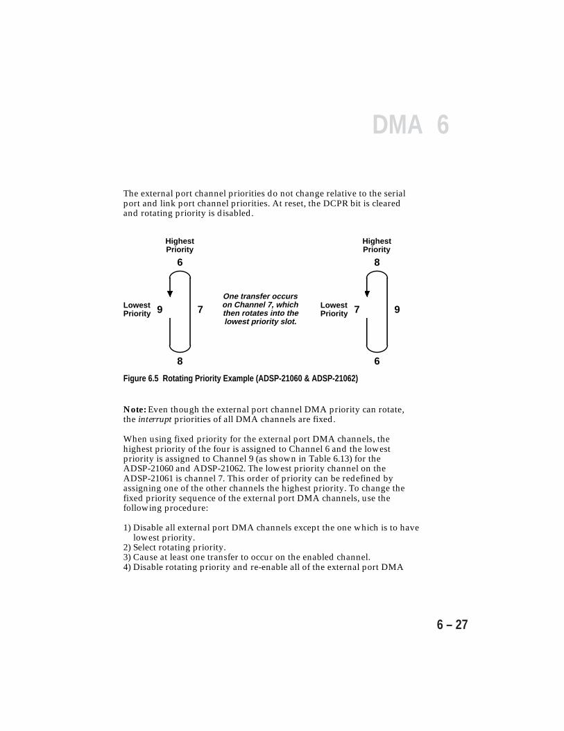
6DMA
6 – 27
The external port channel priorities do not change relative to the serialport and link port channel priorities. At reset, the DCPR bit is clearedand rotating priority is disabled.
Note: Even though the external port channel DMA priority can rotate,the interrupt priorities of all DMA channels are fixed.
When using fixed priority for the external port DMA channels, thehighest priority of the four is assigned to Channel 6 and the lowestpriority is assigned to Channel 9 (as shown in Table 6.13) for theADSP-21060 and ADSP-21062. The lowest priority channel on theADSP-21061 is channel 7. This order of priority can be redefined byassigning one of the other channels the highest priority. To change thefixed priority sequence of the external port DMA channels, use thefollowing procedure:
1) Disable all external port DMA channels except the one which is to havelowest priority.
2) Select rotating priority.3) Cause at least one transfer to occur on the enabled channel.4) Disable rotating priority and re-enable all of the external port DMA
Figure 6.5 Rotating Priority Example (ADSP-21060 & ADSP-21062)
6
8
79
HighestPriority
LowestPriority
8
6
97
HighestPriority
LowestPriority
One transfer occurs on Channel 7, which then rotates into the lowest priority slot.
6 DMA
6 – 28
channels.
The channel immediately after the selected channel will now have thehighest fixed priority, for example (ADSP-21060 & ADSP-21062):
HIGHEST LOWEST
Priority at Reset: DMA6 DMA7 DMA8 DMA9
Follow steps 1-4 above to make DMA7 the lowest priority.
New Priority Ordering: DMA8 DMA9 DMA6 DMA7
6.3.4 DMA ChainingDMA chaining allows the ADSP-2106x’s DMA controller toautoinitialize itself between multiple DMA transfers. Using chaining,you can set up multiple DMA operations in which each operation canhave different attributes.
In chained DMA operations, the ADSP-2106x automatically sets upanother DMA transfer when the entire contents of the current bufferhave been transmitted or received. The chain pointer register (CP) isused to point to the next set of DMA parameters stored in internalmemory. This new set of parameters is called a transfer control block(TCB). The ADSP-2106x’s DMA controller automatically reads the TCBfrom internal memory and loads the values into the channel parameterregisters to set up the next DMA sequence; this process is called TCBchain loading.
A DMA sequence is defined as the sum of the DMA transfers for asingle channel, from the parameter registers initialization to when thecount register decrements to zero.
Each DMA channel has a chaining enable bit (CHEN) in thecorresponding control register. This bit must be set to 1 to enablechaining. Writing all zeros to the address field of the chain pointerregister (CP) also disables chaining.
When chaining is enabled, DMA transfers are initiated by writing amemory address to the CP register. This is also an easy way to start asingle DMA sequence, with no subsequent chained DMAs. The CPregister can be loaded at any time during the DMA sequence—thisallows a DMA channel to have chaining disabled (CP register addressfield = 0x0000) until some event occurs that loads the CP register witha non-zero value. DMA chaining operations may only occur within thesame channel; cross-channel chaining is not supported.

6DMA
6 – 29
The CP register is 18 bits wide, of which the lower 17 bits are thememory address field. The memory address field is offset by0x0002 0000 before it is used by the DMA controller. The mostsignificant bit (bit 17) of the CP register is a control bit called PCI(Program-Controlled Interrupts). The PCI bit selects whether or not aninterrupt occurs at the completion of the current DMA sequence (inaddition to the interrupt’s mask bit in IMASK). When PCI=1, thecorresponding DMA channel interrupt is enabled and will occur whenthe count register reaches zero. When PCI=0, the channel’s interrupt isdisabled. Note that the PCI bit only affects DMA channels for whichchaining is enabled (i.e. CHEN bit set to 1). For non-chained DMAoperations, the IMASK register must be used to disable the interrupt.Interrupt requests enabled by the PCI bit can still be masked out (i.e.disabled) in the IMASK register. Figure 6.6 illustrates the PCI bitwithin the CPx register.
Caution: Because the PCI bit is not part of the memory address in theCP register, care should be taken when writing and reading addressesto and from the register. To prevent errors, it is a good practice tomask out the PCI bit (bit 17) when copying the address in CP toanother address register.
11 10 9 8 7 6 5 4 3 2 1 015 14 13 12
PCI bit
17 16
Memory Address Field (address of next TCB)
CPx
Figure 6.6 Chain Pointer Register & PCI Bit
The general-purpose register (GP) can be useful during chained DMAsequences. It is loaded from memory with the other parameterregisters, and can be used to point to the last DMA sequence that wascompleted. This allows a program to determine where the last full (orempty) data buffer is located. Since it is a general-purpose registerwith no dedicated functionality, it can be used for any purpose.

6 DMA
6 – 30
6.3.4.1 Transfer Control Blocks & Chain LoadingDuring TCB chain loading, the DMA channel parameter registers areloaded with values retrieved from internal memory. The CP registercontains the chain pointer—the highest address of the TCB. The TCB isstored in consecutive locations.
Table 6.14 below shows the TCB-to-register loading sequence for theexternal port, link port, and serial port DMA channels (i.e. the order inwhich the DMA controller reads each word of the TCB and loads itinto the corresponding register.) Figure 6.7 shows how you must setup the TCB in memory (for an external port DMA chain), referenced tothe address pointer contained in the CP register of the previous DMAoperation of the chain.
External Port & Serial Ports &Address_____________ Link Buffers 4,5 Link Buffers 0,1,2,3CPx + 0x0002 0000 IIx IIxCPx – 1 + 0x0002 0000 IMx IMxCPx – 2 + 0x0002 0000 Cx Cx (and DAx for 2D DMA)CPx – 3 + 0x0002 0000 CPx CPxCPx – 4 + 0x0002 0000 GPx GPxCPx – 5 + 0x0002 0000 EIx DBx (loaded during 2D DMA only)CPx – 6 + 0x0002 0000 EMx LPATH1 (mesh multiproc. links only)CPx – 7 + 0x0002 0000 ECx LPATH2 (mesh multiproc. links only)CPx – 8 + 0x0002 0000 – LPATH3 (mesh multiproc. links only)
Table 6.14 TCB Chain Loading Sequence
Notes:
1. An “x” denotes the DMA channel number.2. The DAx and DBx registers are not loaded during chaining in normal, one-
dimensional DMA. In 2D DMA operations, only DBx is loaded. The DAx registeris automatically loaded with the same value as the Cx register. (2D DMAoperations are not applicable to the ADSP-21061.)
3. The link transmit chain also downloads the LPATH1, LPATH2, and LPATH3registers when the LMSP bit in the LCOM control register is set, enabling meshmultiprocessing. (These registers are not available of the ADSP-21061.)
4. Link Buffers 4 and 5 use the same chaining registers as the external port. All 8registers are always loaded when chaining on DMA channels 6-9, but EIx, EMx,and ECx are not used when Link Buffers 4 and 5 are enabled. (Link buffers 4-5are not available on the ADSP-21061.)
A working register is loaded from the CP register before the chainloading sequence begins, and is decremented after each register isloaded. The working register allows the CP register to be updated withthe new CP value without interfering with the current register loading.

6DMA
6 – 31
When the chain loading is complete, the working register is loadedwith the new CP value. This allows chained DMA sequences to be setup in a continuous loop. (Note: The contents of the working registerare not accessible.)
TCB chain loading is requested like all other DMA operations. A TCBloading request is latched and held in the DMA controller until itbecomes the highest priority request. The IOP individually prioritizesand transfers the TCB register like normal DMA. If multiple chainingrequests are present, the TCB registers for the highest priority DMAchannel are transferred first. A channel which is in the process of chainloading cannot be interrupted by a higher priority channel. Refer toTable 6.13 for the DMA channel request priorities.
ECx
EMx
EIx
Address
CPx
Cx
IIx
GPx
IMx
Address pointer to next TCB
Lowest addressCPx – 7
CPx – 6
CPx – 5
CPx – 4
CPx – 3
CPx – 2
CPx – 1
CPx Highest address
Figure 6.7 TCB Setup In Memory (For External Port DMA Channel)
6.3.4.2 Setting Up & Starting The ChainTo setup and initiate a chain of DMA operations, your program shouldfollow this sequence:
1. Set up all TCBs in internal memory.
2. Write to the appropriate DMA control register, setting the DENenable bit to 1 and the CHEN chaining enable bit to 1.
3. Write the last address (i.e. the address of the IIx register value) ofthe first TCB to the CPx register—this will start the chain.
6 DMA
6 – 32
The DMA controller will autoinitialize itself with the first TCB andthen start the first transfer. When this transfer is completed, the nextone will begin if the current chain pointer address is non-zero. Thisaddress will be used as the pointer to the next TCB.
Remember that the address field of the CPx registers is only 17 bitswide. If a symbolic address is written directly to CPx, bit 17 mayconflict with the PCI bit. Be sure to clear the upper bits of the address,then AND in the PCI bit separately if needed.
6.3.4.3 Chain InsertionA high priority DMA operation or chain can be inserted into an activeDMA chain. When CHEN=1 and DEN=0, the DMA channel is placedin chain insertion mode in which a new DMA chain can be inserted intothe current chain without affecting the current DMA transfer. The newchain is inserted by the ADSP-2106x core writing a TCB into thechannel parameter registers. This mode of operation is identical to thatselected by CHEN=1 and DEN=1; except that when the current DMAtransfer ends, automatic chaining is disabled and an interrupt requestoccurs. This interrupt request is independent of the PCI bit state.
The following sequence should be used to insert a DMA subchainwhile another chain is active:
1. Enter chain insertion mode by setting CHEN=1 and DEN=0 in theappropriate DMA control register.
2. The DMA interrupt will indicate when the current DMA sequence hascompleted.
3. Write the CPx register value into the CP position of the last TCB in thenew chain.
4. Set DEN=1 and CHEN=1.
5. Write the start address of the first TCB of the new chain into the CPregister.
Chain insertion should not be set up as an initial mode of operation; itis intended for use only while another DMA operation is in progress.
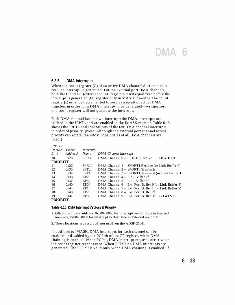
6DMA
6 – 33
6.3.5 DMA InterruptsWhen the count register (C) of an active DMA channel decrements tozero, an interrupt is generated. For the external port DMA channels,both the C and EC (external count) registers must equal zero before theinterrupt is generated (EC register only in MASTER mode). The countregister(s) must be decremented to zero as a result of actual DMAtransfers in order for a DMA interrupt to be generated—writing zeroto a count register will not generate the interrupt.
Each DMA channel has its own interrupt; the DMA interrupts arelatched in the IRPTL and are enabled in the IMASK register. Table 6.15shows the IRPTL and IMASK bits of the ten DMA channel interrupts,in order of priority. (Note: Although the external port channel accesspriority can rotate, the interrupt priorities of all DMA channels arefixed.)
IRPTL/IMASK Vector InterruptBit # Address1 Name DMA Channel Interrupt10 0x28 SPR0I DMA Channel 0 – SPORT0 Receive HIGHESTPRIORITY11 0x2C SPR1I DMA Channel 1 – SPORT1 Receive (or Link Buffer 0)12 0x30 SPT0I DMA Channel 2 – SPORT0 Transmit13 0x34 SPT1I DMA Channel 3 – SPORT1 Transmit (or Link Buffer 1)14 0x38 LP2I DMA Channel 4 – Link Buffer 22
15 0x3C LP3I DMA Channel 5 – Link Buffer 32
16 0x40 EP0I DMA Channel 6 – Ext. Port Buffer 0 (or Link Buffer 4)17 0x44 EP1I DMA Channel 7 – Ext. Port Buffer 1 (or Link Buffer 5)18 0x48 EP2I DMA Channel 8 – Ext. Port Buffer 22
19 0x4C EP3I DMA Channel 9 – Ext. Port Buffer 32 LOWESTPRIORITY
Table 6.15 DMA Interrupt Vectors & Priority
1. Offset from base address: 0x0002 0000 for interrupt vector table in internalmemory, 0x0040 0000 for interrupt vector table in external memory
2. These locations are reserved, not used, on the ADSP-21061.
In addition to IMASK, DMA interrupts for each channel can beenabled or disabled by the PCI bit of the CP register, when DMAchaining is enabled. When PCI=1, DMA interrupt requests occur whenthe count register reaches zero. When PCI=0, no DMA interrupts aregenerated. The PCI bit is valid only when DMA chaining is enabled. If
6 DMA
6 – 34
chaining is disabled, the IMASK register must be used to disableinterrupts. Interrupt requests enabled by PCI can still be masked outby the IMASK register.
DMA interrupts can also be generated by ADSP-2106x’s I/O portswithout using DMA. In this case, a DMA interrupt is generatedwhenever data becomes available at the receive buffer, or wheneverthe transmit buffer does not have new data to transmit. GeneratingDMA interrupts in this fashion is useful for implementing interrupt-driven I/O under control of the ADSP-2106x core processor. Multipleinterrupts can occur if several I/O ports transmit or receive data in thesame cycle. To perform single-word, non-DMA, interrupt-driventransfers on the external port, the INTIO bit must be set in a DMACxcontrol register.
The following list describes the various conditions for which aninterrupt will be generated by a DMA channel or its correspondingI/O port:
InterruptCondition MaskChaining disabled, current DMA sequence completes IMASKChaining enabled, current DMA sequence completes IMASK & PCIChain insertion mode, current DMA sequence completes IMASKDMA disabled and a buffer is accessed by the I/O port* IMASK* INTIO bit must be set in DMACx control register for external port.
If the interrupt mask is a 1 (i.e. unmasked), the interrupt is enabled andwill be acknowledged.
The IMASK register is not directly accessible to external devices, viathe external port, because it is one of the universal registers in theADSP-2106x processor core (and is not memory-mapped like the IOPregisters). IMASK may be read or written via the external port,however, by using an interrupt vector to a routine set up to handle thistask. The VIRPT vector interrupt register may be used for this purpose.
As an alternative to interrupts, polling DMASTAT can be used todetermine when a single DMA sequence has completed:
1. Read DMASTAT.2. If both status bits for the channel are inactive, the DMA sequence has
completed.
6DMA
6 – 35
If chaining is enabled, however, polling DMASTAT should not be usedsince the next DMA sequence may be under way by the time thepolled status is returned.
6.3.6 Starting & Stopping DMA SequencesDMA sequences are started in different ways depending on whetherDMA chaining is enabled. When chaining is not enabled, only theDMA enable bit (DEN) allows DMA transfers to occur.
A DMA sequence starts when one of the following occurs:
• Chaining is disabled and the DMA enable bit (DEN) transitions fromlow to high.
• Chaining is enabled, DMA is enabled (DEN=1), and the CP registeraddress field is written with a non-zero value. (In this case, TCBchain loading of the channel parameter registers occurs first.)
• Chaining is enabled, the CP register address field is non-zero, andthe current DMA sequence finishes. (Again, TCB chain loadingoccurs.)
A DMA sequence ends when one of the following occurs:
• The count register decrements to zero (both C and EC for externalport channels).
• Chaining is disabled and the channel’s DEN bit transitions fromhigh to low. If the DEN bit goes low and chaining is enabled, thechannel enters chain insertion mode and the DMA sequencecontinues. (See “Chain Insertion” for details.)
Note that whenever the DEN bit goes high again, the DMA sequencecontinues from where it left off (for non-chained operations only).
To start a new DMA sequence after the current one is finished, yourprogram must first clear the DEN enable bit, write new parameters tothe II, IM, and C registers, and then set the DEN bit to re-enable DMA.(For chained DMA operations, however, this is not necessary; see“DMA Chaining.”)
Warning: If a DMA operation completes and the count register isrewritten before the DMA enable bit is cleared, the DMA transfer will
6 DMA
6 – 36
restart at the new count.
6.4 EXTERNAL PORT DMAChannels 6, 7, 8, and 9 are the external port DMA channels, which areavailable on the ADSP-21060 and ADSP-21062. On the ADSP-21061,only channels 6-7 are available. These DMA channels allow efficientdata transfers between the ADSP-2106x’s internal memory and externalmemory or devices.
6.4.1 External Port FIFO Buffers (EPBx)DMA Channels 6, 7, 8, and 9 are associated with the external port FIFOdata buffers, EPB0, EPB1, EPB2, and EPB3. Each buffer acts as a six-location FIFO. It has two ports, a read port and a write port. Each portcan be connected to either the EPD (External Port Data) bus or to a localbus which in turn can connect to the IOD (I/O Data) bus, PM Databus, or DM Data bus. (See Figure 6.2.) This structure allows data to bewritten to the FIFO on one port while it is being read from the otherport—allowing DMA transfers at the full processor clock frequency.
The external port FIFO buffers can also be used for non-DMA, single-word data transfers, as described in the Host Interface chapter of thismanual.
Caution: The ADSP-2106x core should not attempt to read or write anEPBx buffer when a DMA operation using that buffer is in progress;this will corrupt the DMA data.
Each external port buffer can be flushed (i.e. cleared) by writing a 1 to theFLSH bit in the corresponding DMACx control register. This should only bedone when DMA is disabled for the channel. The FLSH bit is not latchedinternally and will always be read as a 0. Status can change in the followingcycle. An external port buffer should not be enabled and flushed in thesame cycle.
6.4.1.1 External Port DMA Data PackingEach external port buffer contains data packing logic to allow 16-bit or32-bit external bus words to be packed into 32-bit or 48-bit internalwords. The packing logic is also fully reversible, depending on thesetting of the TRAN bit in the DMACx control register, so that 32-bit or48-bit internal data can be unpacked into 16-bit or 32-bit external word
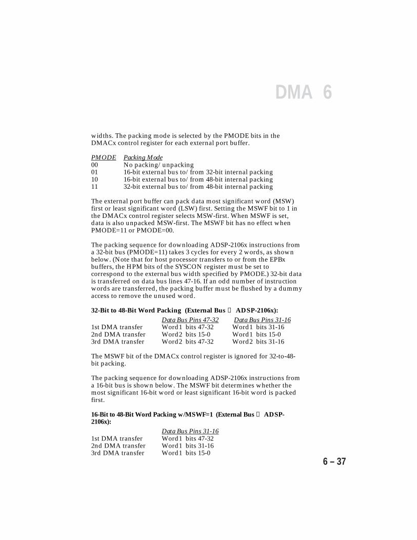
6DMA
6 – 37
widths. The packing mode is selected by the PMODE bits in theDMACx control register for each external port buffer.
PMODE Packing Mode00 No packing/unpacking01 16-bit external bus to/from 32-bit internal packing10 16-bit external bus to/from 48-bit internal packing11 32-bit external bus to/from 48-bit internal packing
The external port buffer can pack data most significant word (MSW)first or least significant word (LSW) first. Setting the MSWF bit to 1 inthe DMACx control register selects MSW-first. When MSWF is set,data is also unpacked MSW-first. The MSWF bit has no effect whenPMODE=11 or PMODE=00.
The packing sequence for downloading ADSP-2106x instructions froma 32-bit bus (PMODE=11) takes 3 cycles for every 2 words, as shownbelow. (Note that for host processor transfers to or from the EPBxbuffers, the HPM bits of the SYSCON register must be set tocorrespond to the external bus width specified by PMODE.) 32-bit datais transferred on data bus lines 47-16. If an odd number of instructionwords are transferred, the packing buffer must be flushed by a dummyaccess to remove the unused word.
32-Bit to 48-Bit Word Packing (External Bus ↔ ADSP-2106x):Data Bus Pins 47-32 Data Bus Pins 31-16
1st DMA transfer Word1 bits 47-32 Word1 bits 31-162nd DMA transfer Word2 bits 15-0 Word1 bits 15-03rd DMA transfer Word2 bits 47-32 Word2 bits 31-16
The MSWF bit of the DMACx control register is ignored for 32-to-48-bit packing.
The packing sequence for downloading ADSP-2106x instructions froma 16-bit bus is shown below. The MSWF bit determines whether themost significant 16-bit word or least significant 16-bit word is packedfirst.
16-Bit to 48-Bit Word Packing w/MSWF=1 (External Bus ↔ ADSP-2106x):
Data Bus Pins 31-161st DMA transfer Word1 bits 47-322nd DMA transfer Word1 bits 31-163rd DMA transfer Word1 bits 15-0
6 DMA
6 – 38
40-bit extended precision data may be transferred using the 48-bitpacking mode. Refer to the Memory chapter of this manual for adescription of memory allocation for different word widths.
6.4.1.2 Packing StatusEach external port DMA control register also contains a two-bit PSfield which contains the number of short words currently packed inthe EPBx buffer. During unpacking, the PS status behaves the same asfor packing. All of the packing functions are available for any type ofDMA transfer.
6.4.2 Internal & External Address GenerationDMA transfers between ADSP-2106x internal memory and externalmemory require the DMA controller to generate addresses for both.The external port DMA channels contain EI (External Index) and EM(External Modifier) registers to perform external address generation.The EI register provides the external port address for the current DMAcycle, and is updated with the modifier value in EM for the nextexternal memory access.
In order to support the wide range of data packing operationsprovided for external DMA transfers, the EI and EM registers are ableto generate addresses at a different rate than the internal addressregisters (II and IM). For this reason the internal and external addressgenerators are decoupled from each other, and the EC (External Count)register is used as the external DMA word counter.
If, for example, a 16-bit DMA device is reading data from ADSP-2106xinternal memory, then two external 16-bit transfers will occur for each32-bit internal memory word and the EC (external) word count shouldbe twice the value of the C (internal) word count.
6.4.3 External Port DMA ModesThe MASTER, HSHAKE, and EXTERN bits of each DMACx controlregister are used to select the DMA mode of operation. Each externalport DMA channel can be set up to operate in one of five DMA modes.The master mode initiates transfers while the other modes act as“slaves” where an external device must initiate each transfer.
The MASTER, HSHAKE, and EXTERN bits configure the DMA mode
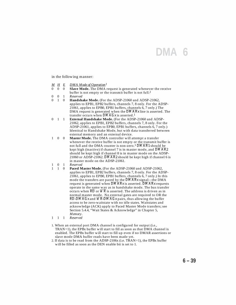
6DMA
6 – 39
in the following manner:
M H E DMA Mode of Operation1
0 0 0 Slave Mode. The DMA request is generated whenever the receivebuffer is not empty or the transmit buffer is not full.2
0 0 1 Reserved0 1 0 Handshake Mode. (For the ADSP-21060 and ADSP-21062,
applies to EPB1, EPB2 buffers, channels 7, 8 only. For the ADSP-21061, applies to EPB0, EPB1 buffers, channels 6, 7 only.) TheDMA request is generated when the DMARx line is asserted. Thetransfer occurs when DMAGx is asserted.1
0 1 1 External Handshake Mode. (For the ADSP-21060 and ADSP-21062, applies to EPB1, EPB2 buffers, channels 7, 8 only. For theADSP-21061, applies to EPB0, EPB1 buffers, channels 6, 7 only.)Identical to Handshake Mode, but with data transferred betweenexternal memory and an external device.
1 0 0 Master Mode. The DMA controller will attempt a transferwhenever the receive buffer is not empty or the transmit buffer isnot full and the DMA counter is non-zero.1 DMAR1 should bekept high (inactive) if channel 7 is in master mode, and DMAR2should be kept high if channel 8 is in master mode on the ADSP-21060 or ADSP-21062. DMAR2 should be kept high if channel 6 isin master mode on the ADSP-21061.
1 0 1 Reserved1 1 0 Paced Master Mode. (For the ADSP-21060 and ADSP-21062,
applies to EPB1, EPB2 buffers, channels 7, 8 only. For the ADSP-21061, applies to EPB0, EPB1 buffers, channels 6, 7 only.) In thismode the transfers are paced by the DMARx signal—the DMArequest is generated when DMARx is asserted. DMARx requestsoperate in the same way as in handshake mode. The bus transferoccurs when RD or WR is asserted. The address is driven as innormal master mode. No external gates are required to OR theRD-DMAGx and WR-DMAGx pairs, thus allowing the bufferaccess to be zero-waitstate with no idle states. Waitstates andacknowledge (ACK) apply to Paced Master Mode transfers; seeSection 5.4.4, “Wait States & Acknowledge” in Chapter 5,Memory.
1 1 1 Reserved
1. When an external port DMA channel is configured for output (i.e.,TRAN=1), the EPBx buffer will start to fill as soon as that DMA channel isenabled. The EPBx buffer will start to fill up even if no DMAR assertions orslave mode DMA buffer reads have been made yet.
2. If data is to be read from the ADSP-2106x (i.e. TRAN=1), the EPBx bufferwill be filled as soon as the DEN enable bit is set to 1.
6 DMA
6 – 40
6.4.3.1 Master ModeWhen the DMACx bits are set such that MASTER=1,HANDSHAKE=0, and EXTERN=0, then the corresponding DMAchannel operates in master mode. This means that the ADSP-2106x’sDMA controller will generate internal DMA requests for that channeluntil the DMA sequence is completed. Master mode can be specifiedindependently for each external port DMA channel.
Examples of DMA master mode operations include transfers betweeninternal memory and external memory and transfers from internalmemory to external devices. In both cases, the data is set up in memoryso that the ADSP-2106x can run the complete sequence withoutinteraction with other devices.
Note: The serial port and link port DMA channels do not have theMASTER control bit and do not operate in master mode.
6.4.3.2 Paced Master ModeIn paced master mode, the DMARx requests operate in the same wayas in handshake mode but DMAGx is not active. The ADSP-2106xresponds to the requests only with the RD or WR strobe; this methodallows the same buffer to be shared for both DMA and core processorI/O without external gating. Paced Master Mode accesses can beextended by the ACK pin, by waitstates programmed in the WAITregister, and by holding the DMARx pin low.
6.4.3.3 Slave ModeWhen the DMACx bits MASTER, HANDSHAKE, and EXTERN arecleared, then the corresponding DMA channel is configured as a slave.This means that the particular DMA channel cannot independentlyinitiate external memory transfers no matter what the programmeddirection of data transfer. To initiate a DMA transfer to or from anADSP-2106x configured in slave mode, an external device must read orwrite to the appropriate EPBx buffer.
If the DMA channel is in slave mode and the direction of data transferis internal to external, the channel will automatically perform enoughtransfers from internal memory to keep the EPBx buffer full.(Remember that each EPBx buffer is a six-location FIFO.) On the otherhand, if the direction of data transfer is external to internal, then theDMA channel will not initiate any internal DMA transfers until the
6DMA
6 – 41
EPBx buffer has valid data.
The EI, EM, and EC registers are not used in slave mode DMA.
External to InternalTo explore the operation of slave mode DMA, consider the case wherean external device wishes to transfer a block of data into the ADSP-2106x’s internal memory. First the external device would write to theDMA channel parameter registers, II, IM, and C, and to the DMACxcontrol register to initialize the channel. Then the device would beginwriting data to the EPBx buffer.
When the EPBx buffer contains a valid data word (requiring one ormore external memory cycles, depending on the packing modeselected), it signals the ADSP-2106x’s DMA controller to request aninternal DMA cycle. When granted, the internal DMA transfer occursand the EPBx buffer FIFO is emptied. If the internal DMA transfer washeld off for some reason, the external device could still write to theEPBx buffer again because of its six-deep FIFO. When the EPBx FIFOeventually becomes full, the external device will be held off with theACK signal (for synchronous accesses) or with the REDY signal (forasynchronous, host-driven accesses).
This state continues until the internal DMA transfer is completed andspace freed up in the EPBx buffer. For the buffer to operate in thisfashion, the BHD (Buffer Hang Disable) bit must be cleared (to 0) in theSYSCON register.
Internal to ExternalNow consider the case where the transfer direction is from internalmemory to the external port. Immediately after the DMA channel isenabled, it will request internal DMA transfers to fill up the EPBx FIFObuffer. Once the buffer is filled, the request will be deasserted. Whenthe external device reads the buffer (one or more times depending onthe packing mode), it becomes “partially empty” and the internalDMA request is asserted again. If the internal DMA transfers cannotfill the EPBx FIFO buffer at the same rate as the external deviceempties it (e.g. due to internal bus conflicts), the external device will beheld off with the ACK signal (for synchronous accesses) or with theREDY signal (for asynchronous, host-driven accesses) until valid datacan be transferred to the EPBx buffer. Again, for the buffer to operatein this fashion, the BHD (Buffer Hang Disable) bit must be cleared (to
6 DMA
6 – 42
0) in the SYSCON register.
Note that ACK (or REDY) is only deasserted during a write when theEPBx FIFO buffer is full. ACK (or REDY) remains asserted at the end ofa completed block transfer if the EPBx buffer is not full. When reading,the buffer will be empty at the end of the block transfer and ACK (orREDY) will be deasserted if an additional read is attempted.
System-Level ConsiderationsSlave mode DMA is useful in systems with a host processor because itallows the host to access any ADSP-2106x internal memory locationwhile limiting the address space the host must recognize—only theaddress space of the ADSP-2106x’s IOP registers. Slave mode DMA isalso useful for ADSP-2106x to ADSP-2106x DMA transfers.
Slave mode DMA has one drawback when interfacing to a slow host—the fact that the external bus is held up during the transfer (whetherinitiated by the ADSP-2106x or the host) and no other transactions canproceed. To overcome this, the handshake DMA mode may be used. Inhandshake mode, the host does not have to master the bus in order tomake a DMA request, nor does the ADSP-2106x (in master mode) haveto wait on the bus for the transfer to complete. Instead, the host assertsthe DMARx pin. When the ADSP-2106x is ready to make the transfer,it can complete it in one bus cycle. The following section providesfurther details.
6.4.3.4 Handshake ModeOn the ADSP-21060 or ADSP-21062, DMA channels 7 and 8, forexternal port buffers EPB1 and EPB2, each have a set of externalhandshake controls. DMAR1 and DMAG1 are the request and grantsignals for EPB1 and channel 7, and DMAR2 and DMAG2 are therequest and grant signals for EPB2 and channel 8.
On the ADSP-21061, DMA channels 7 and 6, for external port buffersEPB1 and EPB0, each have a set of external handshake controls.DMAR1 and DMAG1 are the request and grant signals for EPB1 andchannel 7, and DMAR2 and DMAG2 are the request and grant signalsfor EPB0 and channel 6.
These signals serve as a hardware handshake to facilitate DMAtransfers between the ADSP-2106x and an external peripheral devicethat does not have bus mastership capability.
If external port DMA channel is enabled but the handshakesignals will not be used, the corresponding DMARx signalshould be kept high.
6DMA
6 – 43
Handshake mode DMA is enabled when the HSHAKE bit is set to 1 inthe corresponding DMACx control register (DMAC7 or DMAC8 on anADSP-21060 or ADSP-21062; DMAC7 or DMAC6 on an ADSP-21061).If the MASTER bit is 0, the ADSP-2106x handshakes by returningDMAGx. If the MASTER mode bit is 1, the DMA operates in pacedmaster mode.
DMA handshaking operates asynchronously at up to the full clockspeed of the ADSP-2106x. The data source/destination can be selectedto be either ADSP-2106x internal memory or external memory. It isimportant to load the EC external count register whenever externalDMA transfers are being made.
The MS3-0 memory select lines are deasserted during DMA transfersbetween an external device and an ADSP-2106x because there is noexternal memory space being accessed. The MS3-0 lines are, however,asserted by the ADSP-2106x in external handshake mode because it isproviding the address and strobes for transfers between an externalDMA device and external memory.
Refer to Figure 6.8, DMA Handshake Timing with Asynchronous Requests.The DMA handshake uses the rising and falling edges of DMARx. TheADSP-2106x interprets a falling edge to mean “begin a DMA access”and interprets the rising edge to mean “complete the DMA access.”
To request an access of the EPBx buffer, the external device pullsDMARx low. The falling edge is detected by the ADSP-2106x andsynchronized to the processor’s system clock. To be recognized in aparticular cycle, the DMARx low transition must meet the setup timespecified in the data sheet; otherwise it may take effect in the followingcycle. When the ADSP-2106x recognizes the request, it begins toarbitrate for the external bus, if it is not already the bus master or if thebuffer is not blocked (see discussion of blocked condition below). Whenthe ADSP-2106x becomes the bus master, it drives DMAGx low. TheADSP-2106x will keep DMAGx asserted until it sees DMARxdeasserted. This allows the external device to hold the ADSP-2106xuntil it is ready to proceed. Provided there are no pipelined requests,DMAGx will deassert in the cycle after DMARx is deasserted. If theexternal device does not wish to extend the grant cycle, it can deassertDMARx immediately after asserting it, provided it meets the minimumpulse width timing requirements specified in the data sheet. In thiscase, DMAGx will be a short pulse and the external bus will only beused for one cycle.
6 DMA
6 – 44
The DMA controller has a three-cycle pipeline, similar to thefetch–decode–execute pipeline of the core processor’s programsequencer. The DMA request and arbitration occur in the fetch cycle.The DMA address generation and bus arbitration occur in the decodecycle and the data transfer occurs in the execute cycle. Use of the risingand falling edges of DMARx allows better utilization of the pipelineand, if desired, allows data transfers at up to the full clock rate of theADSP-2106x.
The external device does not have to wait for the DMAGx grant signalbefore making another request. The requests are stored in a workingcounter maintained internally by the ADSP-2106x. The counter holds amaximum of seven requests, so the external device can make up toseven requests before the first one has been serviced. Note that morethan seven requests without a grant will cause unpredictable results.DMAGx will be asserted in response to DMARx only for the numberof transfers specified in the counter. If more requests than this aremade, DMAGx will remain deasserted. The flush bit (FLSH) in theDMACx control register should be used to clear any extra requests.
The external device must make sure that when the DMAGx grantsignal arrives, the data for each write request is immediately available(or that it can accept each word for a read). This can be accomplishedby placing the data in an external FIFO. When DMAing data at the fullclock speed of the ADSP-2106x, a two- or three-deep data pipeline maybe needed to handle the latency between request and grant. Thus, theexternal device might issue three requests rapidly and condition thefourth request on whether a grant has been given in the meantime.Given this caveat, handshake DMA can occur at up to the full clockrate of the ADSP-2106x for both reads and writes. The stored requestsare cleared when a 1 is written to the flush bit (FLSH) in the DMACxcontrol register.
Since the external device can control the completion of a request, itdoes not need to have data available before making a request. If,however, the data is not available within two cycles and DMARx iskept low for this time, the ADSP-2106x and the external bus may beheld inactive. The external bus is occupied for only one cycle for eachDMA transfer if the request is deasserted before the grant has beenasserted. Otherwise the external bus is held as long as DMARx isasserted.
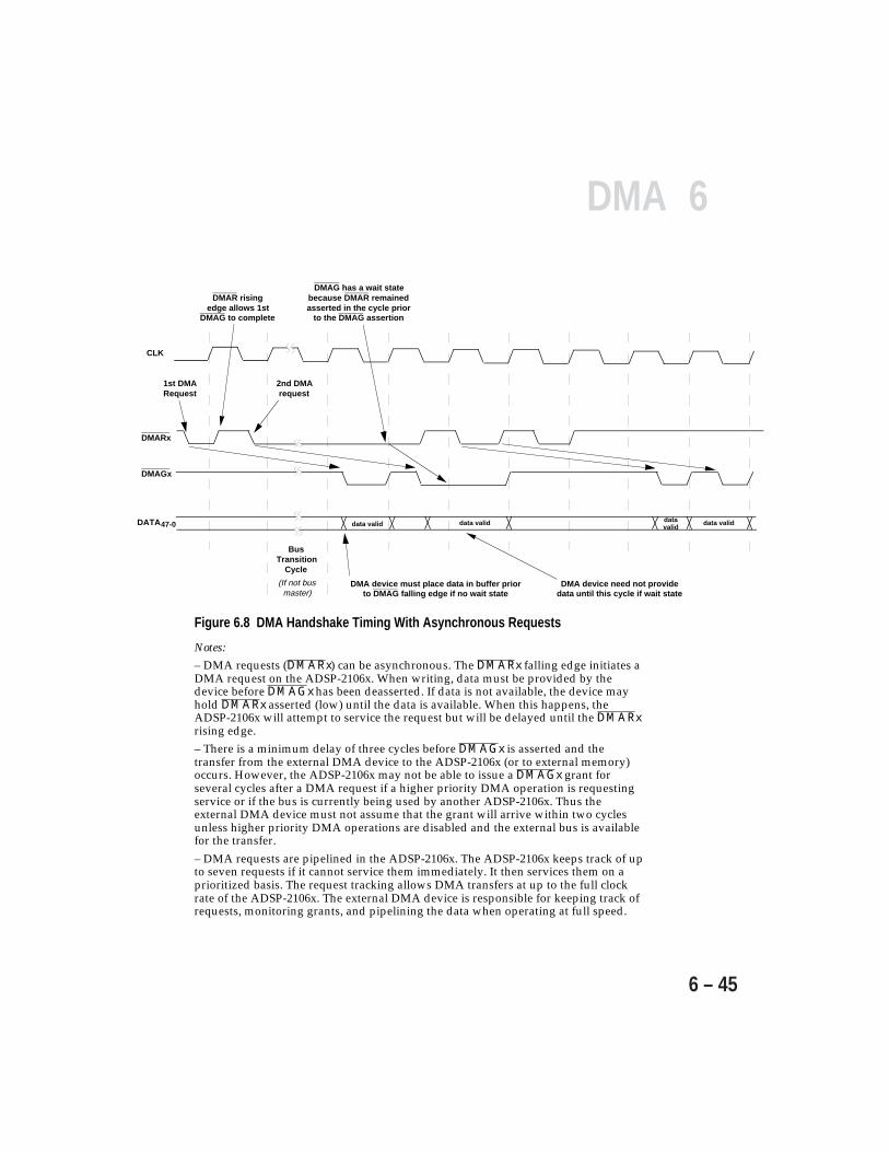
6DMA
6 – 45
CLK
1st DMARequest
DMAR risingedge allows 1st
DMAG to complete
2nd DMArequest
DMAG has a wait state because DMAR remained asserted in the cycle prior
to the DMAG assertion
DMA device must place data in buffer prior to DMAG falling edge if no wait state
DMA device need not provide data until this cycle if wait state
DATA47-0
DMARx
DMAGx
data valid data valid data valid
data valid
Bus Transition
Cycle
(If not bus master)
Figure 6.8 DMA Handshake Timing With Asynchronous Requests
Notes:
– DMA requests (DMARx) can be asynchronous. The DMARx falling edge initiates aDMA request on the ADSP-2106x. When writing, data must be provided by thedevice before DMAGx has been deasserted. If data is not available, the device mayhold DMARx asserted (low) until the data is available. When this happens, theADSP-2106x will attempt to service the request but will be delayed until the DMARxrising edge.– There is a minimum delay of three cycles before DMAGx is asserted and thetransfer from the external DMA device to the ADSP-2106x (or to external memory)occurs. However, the ADSP-2106x may not be able to issue a DMAGx grant forseveral cycles after a DMA request if a higher priority DMA operation is requestingservice or if the bus is currently being used by another ADSP-2106x. Thus theexternal DMA device must not assume that the grant will arrive within two cyclesunless higher priority DMA operations are disabled and the external bus is availablefor the transfer.
– DMA requests are pipelined in the ADSP-2106x. The ADSP-2106x keeps track of upto seven requests if it cannot service them immediately. It then services them on aprioritized basis. The request tracking allows DMA transfers at up to the full clockrate of the ADSP-2106x. The external DMA device is responsible for keeping track ofrequests, monitoring grants, and pipelining the data when operating at full speed.
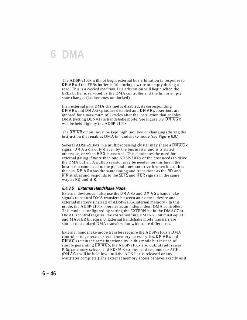
6 DMA
6 – 46
The ADSP-2106x will not begin external bus arbitration in response toDMARx if the EPBx buffer is full during a write or empty during aread. This is a blocked condition. Bus arbitration will begin when theEPBx buffer is serviced by the DMA controller and the full or emptystate changes (i.e. becomes unblocked).
If an external port DMA channel is disabled, its correspondingDMARx and DMAGx pins are disabled and DMARx assertions areignored for a maximum of 2 cycles after the instruction that enablesDMA (setting DEN=1) in handshake mode. See Figure 6.9. DMAGxwill be held high by the ADSP-2106x.
The DMARx input must be kept high (not low or changing) during theinstruction that enables DMA in handshake mode (see Figure 6.9.)
Several ADSP-2106xs in a multiprocessing cluster may share a DMAGxsignal. DMAGx is only driven by the bus master and is tristatedotherwise, or when HBG is asserted. This eliminates the need forexternal gating if more than one ADSP-2106x or the host needs to drivethe DMA buffer. A pullup resistor may be needed on this line if thehost is not connected to the pin and does not drive it when it acquiresthe bus. DMAGx has the same timing and transitions as the RD andWR strobes and responds to the SBTS and HBR signals in the sameway as RD and WR.
6.4.3.5 External Handshake ModeExternal devices can also use the DMARx and DMAGx handshakesignals to control DMA transfers between an external device andexternal memory (instead of ADSP-2106x internal memory). In thismode, the ADSP-2106x operates as an independent DMA controller.This mode is configured by setting the EXTERN bit in the DMAC7 orDMAC8 control register; the corresponding HSHAKE bit must equal 1and MASTER bit equal 0. External handshake mode transfers aresimilar to standard DMA transfers, but with some differences.
External handshake mode transfers require the ADSP-2106x’s DMAcontroller to generate external memory access cycles. DMARx andDMAGx retain the same functionality in this mode but instead ofsimply generating DMAGx, the ADSP-2106x also outputs addresses,MS3-0 memory selects, and RD/WR strobes, and responds to ACK.(DMAGx will be held low until the ACK line is released or anywaitstates complete.) The external memory access behaves exactly as if
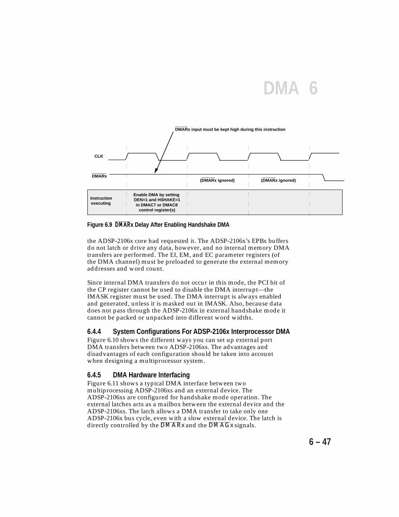
6DMA
6 – 47
CLK
DMARx
Instruction executing
Enable DMA by setting DEN=1 and HSHAKE=1 in DMAC7 or DMAC8
control register(s)
(DMARx ignored) (DMARx ignored)
DMARx input must be kept high during this instruction
Figure 6.9 DMARDMARx Delay After Enabling Handshake DMA
the ADSP-2106x core had requested it. The ADSP-2106x’s EPBx buffersdo not latch or drive any data, however, and no internal memory DMAtransfers are performed. The EI, EM, and EC parameter registers (ofthe DMA channel) must be preloaded to generate the external memoryaddresses and word count.
Since internal DMA transfers do not occur in this mode, the PCI bit ofthe CP register cannot be used to disable the DMA interrupt—theIMASK register must be used. The DMA interrupt is always enabledand generated, unless it is masked out in IMASK. Also, because datadoes not pass through the ADSP-2106x in external handshake mode itcannot be packed or unpacked into different word widths.
6.4.4 System Configurations For ADSP-2106x Interprocessor DMAFigure 6.10 shows the different ways you can set up external portDMA transfers between two ADSP-2106xs. The advantages anddisadvantages of each configuration should be taken into accountwhen designing a multiprocessor system.
6.4.5 DMA Hardware InterfacingFigure 6.11 shows a typical DMA interface between twomultiprocessing ADSP-2106xs and an external device. TheADSP-2106xs are configured for handshake mode operation. Theexternal latches acts as a mailbox between the external device and theADSP-2106xs. The latch allows a DMA transfer to take only oneADSP-2106x bus cycle, even with a slow external device. The latch isdirectly controlled by the DMARx and the DMAGx signals.

6 DMA
6 – 48
If the external device is writing data to the latch, the DMAGx signal isused as the output enable signal for the latch. If the external device isreading from the latch, DMAGx is used to clock the data on its risingedge. Figure 6.12 shows the timing relationships between DMARx,DMAGx, and the data transfer. Refer to the ADSP-2106x Data Sheet forexact specifications.
6.5 DMA THROUGHPUTThis section discusses overall DMA throughput when several DMAchannels are trying to access internal or external memory at the sametime.
Internal Memory DMAThe DMA channels arbitrate for access to the ADSP-2106x’s internalmemory. The DMA controller determines, on a cycle-by-cycle basis,which channel is allowed access to the internal I/O bus andconsequently which channel will read or write to internal memory.(The priority of the DMA channels is shown in Table 6.13 in the “DMAChannel Prioritization” section of this chapter.)
Each DMA transfer takes one clock cycle even when different DMAchannels are being allowed access on sequential cycles; i.e. there is nooverall throughput loss in switching between channels. Thus, four linkport DMA channels, each transferring one byte per cycle, would havethe same I/O transfer rate as one external port DMA channeltransferring data to internal memory on every cycle. Any combinationof link ports, serial ports, and external port transfers has the samemaximum transfer rate.
External Memory DMAWhen the DMA transfer is between ADSP-2106x internal memory andexternal memory, the external memory may have one or more waitstates. External memory wait states, however, do not reduce theoverall internal DMA transfer rate if other channels have dataavailable to transfer. In other words, the ADSP-2106x’s internal I/Odata bus will not be held up by an incomplete external transfer.
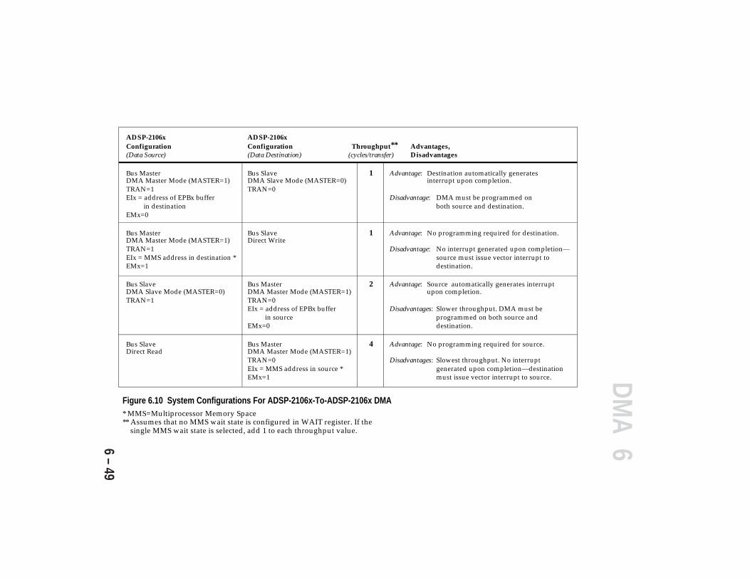
6DM
A
6 – 49
ADSP-2106x ADSP-2106xConfiguration Configuration Throughput Advantages,(Data Source) (Data Destination) (cycles/transfer) Disadvantages
Bus Master Bus Slave 1 Advantage: Destination automatically generatesDMA Master Mode (MASTER=1) DMA Slave Mode (MASTER=0) interrupt upon completion.TRAN=1 TRAN=0EIx = address of EPBx buffer Disadvantage: DMA must be programmed on in destination both source and destination.EMx=0
Bus Master Bus Slave 1 Advantage: No programming required for destination.DMA Master Mode (MASTER=1) Direct WriteTRAN=1 Disadvantage: No interrupt generated upon completion—EIx = MMS address in destination * source must issue vector interrupt toEMx=1 destination.
Bus Slave Bus Master 2 Advantage: Source automatically generates interruptDMA Slave Mode (MASTER=0) DMA Master Mode (MASTER=1) upon completion.TRAN=1 TRAN=0
EIx = address of EPBx buffer Disadvantages: Slower throughput. DMA must be in source programmed on both source andEMx=0 destination.
Bus Slave Bus Master 4 Advantage: No programming required for source.Direct Read DMA Master Mode (MASTER=1)
TRAN=0 Disadvantages: Slowest throughput. No interruptEIx = MMS address in source * generated upon completion—destinationEMx=1 must issue vector interrupt to source.
**
Figure 6.10 System Configurations For ADSP-2106x-To-ADSP-2106x DMA* MMS=Multiprocessor Memory Space** Assumes that no MMS wait state is configured in WAIT register. If the single MMS wait state is selected, add 1 to each throughput value.
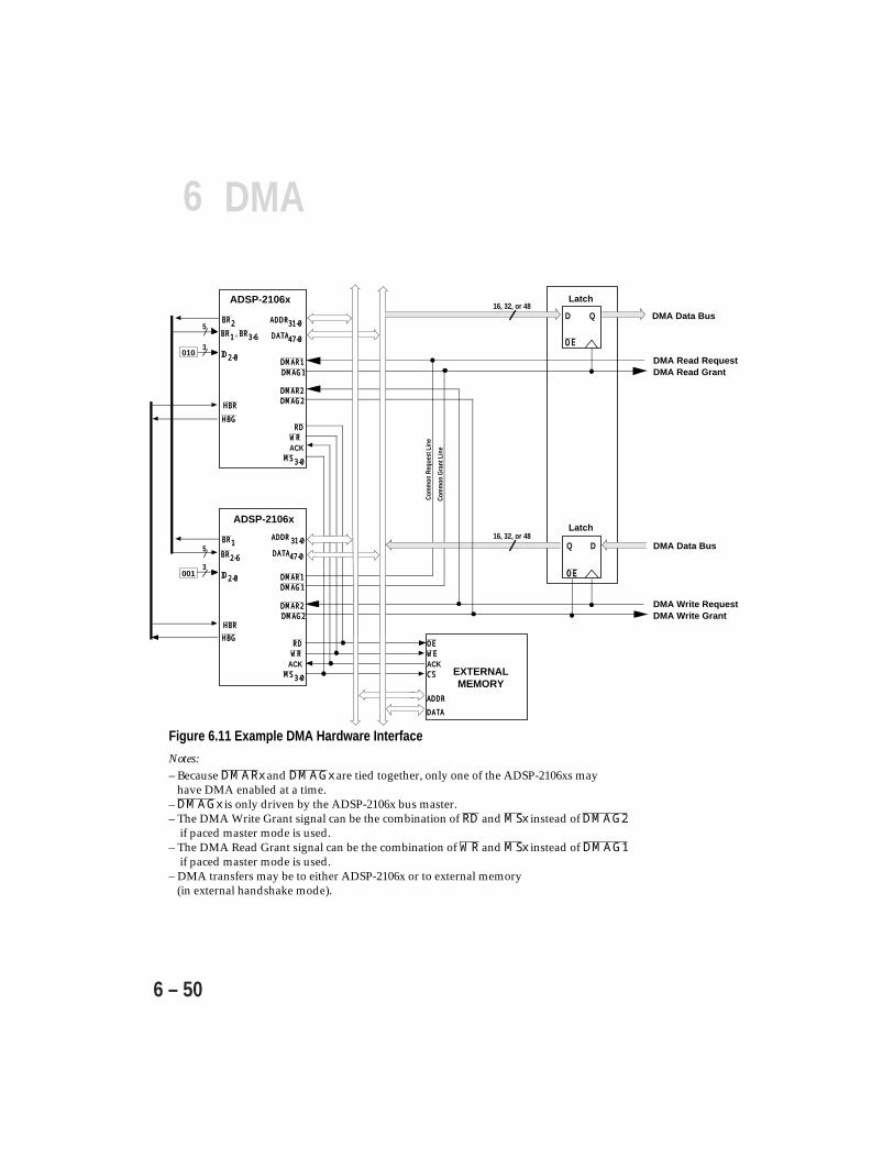
6 DMA
6 – 50
Figure 6.11 Example DMA Hardware Interface
Notes:– Because DMARx and DMAGx are tied together, only one of the ADSP-2106xs may have DMA enabled at a time.– DMAGx is only driven by the ADSP-2106x bus master.– The DMA Write Grant signal can be the combination of RD and MSx instead of DMAG2 if paced master mode is used.– The DMA Read Grant signal can be the combination of WR and MSx instead of DMAG1 if paced master mode is used.– DMA transfers may be to either ADSP-2106x or to external memory (in external handshake mode).
ADDRADDR
DATADATA
EXTERNALMEMORY
CSCSACKWEWEOEOE
ADSP-2106x
ADDADDRR31-031-0DATADATA47-047-0
IDID2-02-0
ADSP-2106x
ADDRADDR31-031-0DATADATA47-047-0
IDID2-02-0
RDRDWRWR
ACKMSMS3-03-0
HBRHBRHBGHBG
BRBR2-62-6
BRBR11
001
010
, BRBR3-63-6BRBR11
5
3
3
BRBR225
DMAG1DMAG1DMAR1DMAR1
DMAG2DMAG2DMAR2DMAR2
HBRHBR
HBGHBGRDRD
WRWRACK
MSMS3-03-0
DMAG1DMAG1DMAR1DMAR1
DMAG2DMAG2DMAR2DMAR2
Q
OEOE
D
DMA Write RequestDMA Write Grant
Com
mon
Req
uest
Lin
e
Com
mon
Gra
nt L
ine
D
OEOE
Q
DMA Read RequestDMA Read Grant
16, 32, or 48
16, 32, or 48DMA Data Bus
DMA Data Bus
Latch
Latch
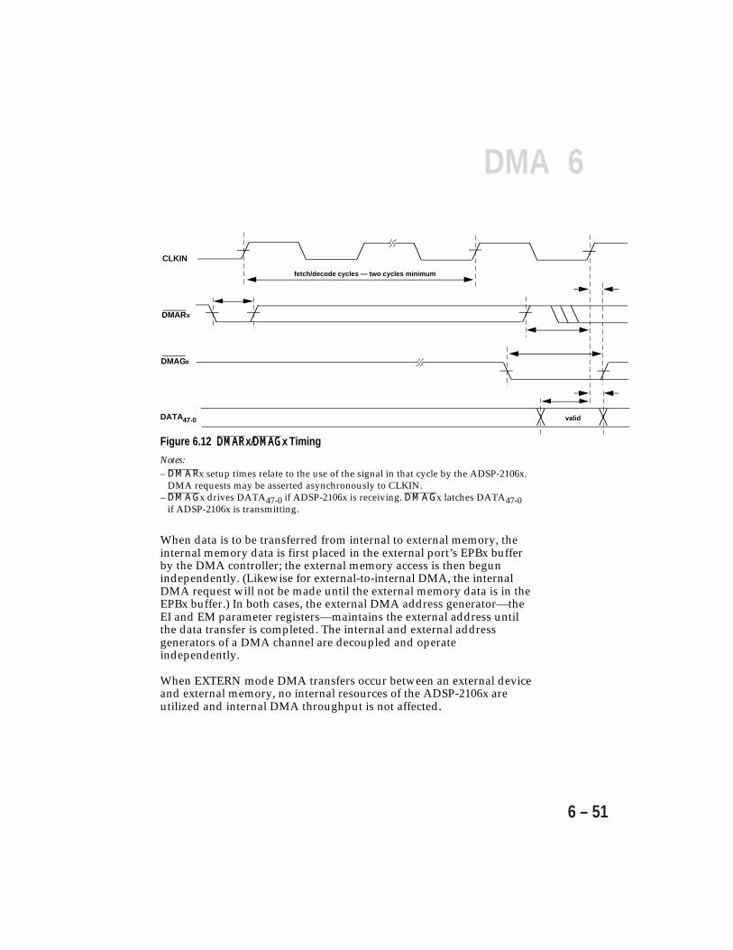
6DMA
6 – 51
fetch/decode cycles — two cycles minimum
CLKIN
DMARx
DMAGx
DATA47-0 valid
Figure 6.12 DMARDMARx/x/DMAGDMAGxx Timing
Notes:– DMARx setup times relate to the use of the signal in that cycle by the ADSP-2106x. DMA requests may be asserted asynchronously to CLKIN.– DMAGx drives DATA47-0 if ADSP-2106x is receiving. DMAGx latches DATA47-0 if ADSP-2106x is transmitting.
When data is to be transferred from internal to external memory, theinternal memory data is first placed in the external port’s EPBx bufferby the DMA controller; the external memory access is then begunindependently. (Likewise for external-to-internal DMA, the internalDMA request will not be made until the external memory data is in theEPBx buffer.) In both cases, the external DMA address generator—theEI and EM parameter registers—maintains the external address untilthe data transfer is completed. The internal and external addressgenerators of a DMA channel are decoupled and operateindependently.
When EXTERN mode DMA transfers occur between an external deviceand external memory, no internal resources of the ADSP-2106x areutilized and internal DMA throughput is not affected.
6 DMA
6 – 52
6.6 TWO-DIMENSIONAL DMAThis section describes the changes in functionality that occur when theADSP-21060 or ADSP-21062 is placed in two-dimensional DMA mode.(Note that two-dimensional DMA mode does not apply to the ADSP-21061.) 2-D DMA mode is enabled by the L2DDMA bit in the LCOMcontrol register and the D2DMA bit in the SRCTL0 and SRCTL1registers. If a particular mode of operation is not explicitly mentionedbelow, then it is unchanged in 2-D mode.
6.6.1 2-D DMA Channel OrganizationIn 2-D mode, two-dimensional DMA array addressing can beperformed for the link buffers and serial ports. DMA channels 0-5support 2-D DMA. Link buffers 4 and 5 (DMA channels 6 and 7) donot support 2-D DMA. Table 6.16 shows the 2-D registers and theirmapping into the DMA channel registers. For the purpose ofdiscussion here, the 2-D array is addressed in row-major order.
DMA2-D ChannelFunction RegisterIndex (address) IIxX Increment IMxX Count CxNext Pointer CPxY Increment DBxY Count GPxX Initial Count DAx (not part of chain; loaded by Cx)
Table 6.16 2-D Register Mapping
In Table 6.16 the DMA channel number, x, is distinguished from thestandard numbering of serial ports and link ports as follows:
Transmit Link Buffer – Uses DMA Channel 5Receive Link Buffer – Uses DMA Channel 4Transmit SPORT – Uses DMA Channel 3 or 1Receive SPORT – Uses DMA Channel 2 or 0
The Index register (II) is loaded with the first address in the data array andmaintains the current address by subtracting the X increment after eachtransfer. The X Increment register (IM) contains the offset added to thecurrent address to point to the next element in the X dimension (nextcolumn). The X Initial Count register (DA) contains the number of data
6DMA
6 – 53
elements in the X dimension. This is used to reload the X count registerwhen it decrements to zero. The X Count register (C) contains the numberof data elements left in the current row. This initially has the same valueas X initial count. It is decremented after each transfer.
The Y Increment register (DB) contains the offset added to the currentaddress to point to the next element in the Y dimension (first locationin next row). When the X count register reaches zero, this register isadded to the current address on the following cycle and the Y countregister is decremented. The value of DB should be the row distanceminus the column distance since both the X and Y increments are doneon a row change. Note that two DMA cycles are required for a rowchange.
The Y Count register (GP) initially contains the number of dataelements in the Y dimension (number of rows). It is decremented eachtime the X count register reaches zero. When Y Count reaches zero, theDMA block transfer is done. The Next Pointer register (CP) points tothe start of a buffer in internal memory containing the next set of DMAparameters.
The DMA controller and the link ports communicate via the sameinternal DMA request/grant handshake as is used by the other I/Oports. The receive link buffer uses channel 4 while the transmit linkbuffer uses channel 5. For more information, refer to the Link Portschapter of this manual. The DMA controller and the serial port alsocommunicate via the same internal DMA request/grant handshake asis used by the other I/O ports. For more information, refer to the SerialPorts chapter.
6.6.2 2-D DMA OperationA two-dimensional DMA transfer occurs in the following manner:
First cycle:• The current address stored in the II register is output and a DMA
memory cycle is started.• In the same cycle, the X Increment value stored in the IM register is
added to the current address in the II register.• The X Count in the C register is decremented.• If the decremented X Count is zero, do the second cycle.

6 DMA
6 – 54
Second cycle:• The X Count is restored into the C register from the DA register.• The Y Increment value in the DB register is added to the current
address in II.• The Y Count in GP is decremented.• If the Y Count is zero, the DMA sequence is ended and the channel
becomes inactive until the Next Pointer is written again.
A key point about the 2-D DMA sequence (or any DMA sequence) isthat the first DMA transfer begins before the address is modified. Thismeans that DMA cannot be disabled by setting either the X Count orthe Y Count to zero. To do one-dimensional DMA transfers in 2-Dmode, the Y Count must be initialized to one.
When the X Count becomes zero but the Y Count is non-zero, theX Count must be reloaded with the original value. The C registerfunctions as the working count register. The DA register holds theoriginal count value. C is loaded from DA to restore the count. The DAregister is written automatically whenever the C register is written.
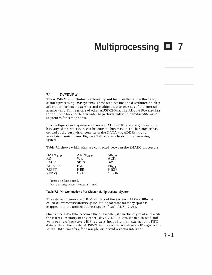
7
7 – 1
Multiprocessing
7.1 OVERVIEWThe ADSP-2106x includes functionality and features that allow the designof multiprocessing DSP systems. These features include distributed on-chiparbitration for bus mastership and multiprocessor accesses of the internalmemory and IOP registers of other ADSP-2106xs. The ADSP-2106x also hasthe ability to lock the bus in order to perform indivisible read-modify-writesequences for semaphores.
In a multiprocessor system with several ADSP-2106xs sharing the externalbus, any of the processors can become the bus master. The bus master hascontrol of the bus, which consists of the DATA47-0, ADDR31-0, andassociated control lines. Figure 7.1 illustrates a basic multiprocessingsystem.
Table 7.1 shows which pins are connected between the SHARC processors.
DATA47-0 ADDR31-0 MS3-0RD WR ACKPAGE SBTS SWADRCLK BMS BR6-1RESET HBR† HBG†REDY† CPA‡ CLKIN
† If Host Interface is used.‡ If Core Priority Access function is used.
Table 7.1 Pin Connections For Cluster Multiprocessor System
The internal memory and IOP registers of the system’s ADSP-2106xs iscalled multiprocessor memory space. Multiprocessor memory space ismapped into the unified address space of each ADSP-2106x.
Once an ADSP-2106x becomes the bus master, it can directly read and writethe internal memory of any other (slave) ADSP-2106x. It can also read andwrite to any of the slave’s IOP registers, including their external port FIFOdata buffers. The master ADSP-2106x may write to a slave’s IOP registers toset up DMA transfers, for example, or to send a vector interrupt.

7 Multiprocessing
7 – 2Figure 7.1 ADSP-2106x Multiprocessor System
ADSP-2106x #6
ADSP-2106x #5
ADSP-2106x #4
ADSP-2106x #3
1x CLOCK1x CLOCK
RESETRESET
CSCS
BOOT BOOT EPROMEPROM
(OPTIONAL)
ADDRADDRDATADATA GLOBALGLOBAL
MEMORY &MEMORY &PERIPHERALSPERIPHERALS
(OPTIONAL)
CSCSACKWEWEOEOE
ADDR
ESS
ADDR
ESS
DATA
DATA
MEM
ORY
CONT
ROL
MEM
ORY
CONT
ROL
ADDRADDR
DATADATA
ADDRADDRDATADATA
(OPTIONAL)
HOSTHOSTINTERFACEINTERFACE
HOST
INTE
RFAC
EHO
ST IN
TERF
ACE
CSCSHBRHBR
REDYREDYHBGHBG
BMSBMS
ADSP-2106x #1
ADDADDRR31-031-0DATADATA47-047-0
RDRDWRWR
ACKMSMS3-03-0
SBTSSBTSPAGEPAGE
SWSWADRCLKADRCLK
CLKINCLKIN
RESETRESET
0 / 1 RPBARPBA
IDID2-02-0
BRBR2-62-6BRBR11
5CPACPA
0013
HOSTINTERFACE
MEMORYCONTROL
BUS
ARBI
TRAT
ION
BUS
ARBI
TRAT
ION
ADSP-2106x #2
ADDADDRR31-031-0DATADATA47-047-0
CLKINCLKIN
RESETRESET
HOSTINTERFACE
MEMORYCONTROL
IDID2-02-0010
3
, BRBR3-63-6BRBR11BRBR22
5CPACPA
RPBARPBA
ADDR
ESS
ADDR
ESS
DATA
DATA
MEM
ORY
CONT
ROL
MEM
ORY
CONT
ROL
HOST
INTE
RFAC
EHO
ST IN
TERF
ACE
BUS
ARBI
TRAT
ION
BUS
ARBI
TRAT
ION

7Multiprocessing
7 – 3
The following terms are used throughout this chapter, and are definedbelow for reference:
external bus DATA47-0 , ADDR31-0 , RD, WR, MS3-0, BMS,ADRCLK, PAGE, SW, ACK, and SBTS signals
multiprocessor system a system with multiple ADSP-2106xs, with orwithout a host processor; the ADSP-2106xs areconnected by the external bus and/or link ports
multiprocessor memory space portion of the ADSP-2106x’s memory map thatincludes the internal memory and IOP registersof each ADSP-2106x in a multiprocessing system;this address space is mapped into the unifiedaddress space of the ADSP-2106x
IOP register one of the control, status, or data buffer registersof the ADSP-2106x’s on-chip I/O processor
bus slave or slave mode an ADSP-2106x can be a bus slave to anotherADSP-2106x or to a host processor
direct reads & writes a direct access of the ADSP-2106x’s internalmemory or IOP registers by another ADSP-2106xor by a host processor
single-word data transfers reads and writes to the EPBx external portbuffers, performed externally by the ADSP-2106xbus master or internally by the ADSP-2106xslave’s core; these occur when DMA is disabledin the DMACx control register
bus transition cycle (BTC) a cycle in which control of the external bus ispassed from one ADSP-2106x to another
external port FIFO buffers EPB0, EPB1, EPB2, and EPB3, the IOP registersused for external port DMA transfers andsingle-word data transfers (from otherADSP-2106xs or from a host processor); the EPBxbuffers are 6-deep FIFOs
DMACx control registers the DMA control registers for the EPBx externalport buffers: DMAC6, DMAC7, DMAC8, andDMAC9, corresponding respectively to EPB0,EPB1, EPB2, and EPB3 (see the DMA chapter orControl/Status Registers appendix of this manualfor a complete description of the DMACx controlregisters)

7 Multiprocessing
7 – 4
7.2 MULTIPROCESSING SYSTEM ARCHITECTURESMultiprocessor systems typically use one of two schemes tocommunicate between processor nodes. One scheme uses dedicatedpoint-to-point communication channels. In the other, nodescommunicate through a single shared global memory via a parallelbus.
The ADSP-2106x SHARC supports the implementation of point-to-point communication through its six link ports. It also supports anenhanced version of shared parallel bus communication called clustermultiprocessing. Cluster multiprocessing features of the ADSP-2106xare described in this chapter, while point-to-point connections aredescribed in the Link Ports chapter of this manual.
Multiprocessing systems must overcome two problems: interprocessorcommunication overhead and data bandwidth bottlenecks. The ADSP-2106x SHARC architecture addresses these concerns in several ways,as illustrated in the following discussion of three basic multiprocessingtopologies.
7.2.1 Data Flow MultiprocessingData flow multiprocessing is best suited for applications requiringhigh computational bandwidth but only limited flexibility.Programmers partition their algorithm sequentially across multipleprocessors and pass data linearly down an “assembly line” ofprocessors, as shown in Figure 7.2.
ADSP-2106x
LinkPort
LinkPort
Data
ADSP-2106x
LinkPort
LinkPort
ADSP-2106x
LinkPort
LinkPort
Figure 7.2 Data Flow Multiprocessing

7Multiprocessing
7 – 5
The ADSP-2106x SHARC is ideally suited for data flowmultiprocessing applications because it eliminates the need forinterprocessor data FIFOs and external memory. The internal memoryof the SHARC is usually large enough to contain both code and datafor most applications using this topology. All a data flow systemrequires are a number of SHARC processors and point-to-point signalsconnecting them. This yields a substantial savings in complexity, boardspace, and system cost.
7.2.2 Cluster MultiprocessingCluster multiprocessing is best suited for applications where a fairamount of flexibility is required. This is especially true when a systemmust be able to support a variety of different tasks, some of which maybe running concurrently. The cluster multiprocessing configuration isshown in Figure 7.3. SHARC processors also have an on-chip hostinterface that allows a cluster to be easily interfaced to a host processoror even to another cluster.
ADSP-2106x
LinkPort
ADSP-2106x
LinkPort
LinkPort
ADSP-2106x
LinkPort
External Port External Port External Port
Bulk Memory
Figure 7.3 Cluster Multiprocessing
7 Multiprocessing
7 – 6
Cluster multiprocessing systems include multiple SHARC processorsconnected by a parallel bus that allows interprocessor access of on-chipmemory as well as access to shared global memory. In a typical clusterof SHARCs, up to six processors and a host can arbitrate for the bus.The on-chip bus arbitration logic allows these processors to share thecommon bus. The SHARC’s other on-chip features help eliminate theneed for any extra hardware in the cluster multiprocessorconfiguration. External memory, both local and global, can frequentlybe eliminated in this type of system.
Both fixed and rotating priority schemes are supported as well as buslocking, timed release, and core processor access preemption ofbackground DMA transfers. The on-chip arbitration logic allowstransitions in bus mastership to take up to only one cycle of overhead.Bus requests are generated implicitly whenever a processor accesses anexternal address. Because each processor monitors all bus requests andapplies the same priority logic to the requests, each can independentlydetermine who will be the next bus master. With complete bus sharingfeatures built into the processor, designers are spared the time and riskof developing their own shared-bus logic and timing.
Once a SHARC gains mastership of the bus, it can access not onlyexternal memory but also the internal memory and IOP registers of allother processors. A processor can directly transfer data to anotherprocessor or set up a DMA channel to transfer the data. Each of theprocessors are mapped into a common memory map—to identify theaddress space of each processor within the unified memory map of thesystem cluster, each processor has a unique ID. The SHARC’s IOPregisters, internal memory, and external memory are all part of theunified address space. This shared on-chip memory eliminates theneed to use external memory for message passing between processorsand simplifies software communications. Processors can write directlyinto each other’s memory, saving an extra transfer step. Local memorymay also no longer be needed due to the SHARC’s large amount of on-chip SRAM. For larger applications, however, blocks of data and codecan be stored in shared bulk memory and transparently swapped inand out of a processor’s internal memory.
7Multiprocessing
7 – 7
Communication between processors is also facilitated by the ability ofa processor to broadcast a write to all processors simultaneously. Thiscan be used to implement reflective semaphores, where a processorpolls its own internal copy of the semaphore and only uses the externalbus for a broadcast write to all other processors when it wants tochange it. This reduces communications traffic on the external bus.
The cluster configuration allows the SHARCs to have a very fast node-to-node data transfer rate. It also allows for a simple, efficient, softwarecommunication model. For example, all of the required setupoperations for a DMA transfer can be accomplished by a singleSHARC on one side of the transfer. The other processor is notinterrupted until the DMA transfer is complete.
The SHARC’s internal memory is designed to facilitate the I/O needsof multiprocessor systems. The on-chip dual-ported RAM allows full-speed interprocessor transfers concurrent with dual accesses by theprocessor’s computational core. No cycles are stolen from the core, andthe processor’s full 40 MIPS, 120 MFLOPS performance is maintained.
7.2.2.1 Link Port Data Transfers In A ClusterA bottleneck exists within the cluster because only two processors cancommunicate over the shared bus during each cycle—other processorsare held off until the bus is released. Since the SHARC can alsoperform point-to-point link port transfers within a cluster, thisbottleneck is easily eliminated. Data links between processors can bedynamically set up and initiated over the common bus. All six linkports can operate simultaneously on each processor.
A disadvantage of the link ports is that individual transfers occur atonly 40 Mbyte/sec (for a 40 MHz system clock), a lower rate than thatof the shared parallel bus. Since the link ports’ 4-bit data path issmaller than the processor’s native word size, the transfer of each wordrequires multiple clock cycles. Link ports may also require moresoftware overhead and complexity because they must be set up onboth sides of the transfers before they can occur.
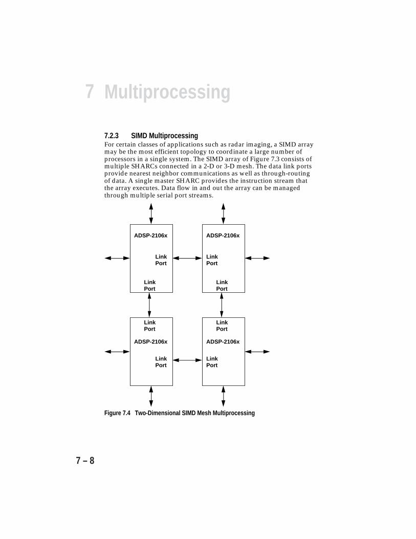
7 Multiprocessing
7 – 8
7.2.3 SIMD MultiprocessingFor certain classes of applications such as radar imaging, a SIMD arraymay be the most efficient topology to coordinate a large number ofprocessors in a single system. The SIMD array of Figure 7.3 consists ofmultiple SHARCs connected in a 2-D or 3-D mesh. The data link portsprovide nearest neighbor communications as well as through-routingof data. A single master SHARC provides the instruction stream thatthe array executes. Data flow in and out the array can be managedthrough multiple serial port streams.
ADSP-2106x
LinkPort
ADSP-2106x
LinkPort
ADSP-2106x
LinkPort
ADSP-2106x
LinkPort
LinkPort
LinkPort
LinkPort
LinkPort
Figure 7.4 Two-Dimensional SIMD Mesh Multiprocessing
7Multiprocessing
7 – 9
7.3 MULTIPROCESSOR BUS ARBITRATIONMultiple ADSP-2106xs can share the external bus with no additionalarbitration circuitry. Arbitration logic is included on-chip to allow theconnection of up to six ADSP-2106xs and a host processor.
Bus arbitration is accomplished with the use of the BR1–BR6, HBR, andHBG signals. BR1–BR6 arbitrate between multiple ADSP-2106xs, andHBR–HBG pass control of the bus from the ADSP-2106x bus master tothe host (and back). The priority scheme for bus arbitration isdetermined by the setting of the RPBA pin. Table 7.2 defines theADSP-2106x pins used in multiprocessing systems.
Signal Type Definition
BR6-1 I/O/S Multiprocessing Bus Requests. Used bymultiprocessing ADSP-2106xs to arbitrate for busmastership. An ADSP-2106x only drives its own BRxline (corresponding to the value of its ID2-0 inputs) andmonitors all others. In a multiprocessor system with lessthan six ADSP-2106xs, the unused BRx pins should betied high; the processor’s own BRx line must not be tiedhigh or low because it is an output.
ID2-0 I Multiprocessing ID. Determines which multiprocessingbus request (BR1 – BR6) is used by ADSP-2106x. ID=001corresponds to BR1, ID=010 corresponds to BR2, etc.ID=000 in single-processor systems. These lines are asystem configuration selection which should behardwired or only changed at reset.
RPBA I/S Rotating Priority Bus Arbitration Select. When RPBAis high, rotating priority for multiprocessor busarbitration is selected. When RPBA is low, fixed priorityis selected. This signal is a system configurationselection which must be set to the same value on everyADSP-2106x. If the value of RPBA is changed duringsystem operation, it must be changed in the sameCLKIN cycle on every ADSP-2106x.
CPA (o/d) I/O Core Priority Access. Asserting its CPA pin allows thecore processor of an ADSP-2106x bus slave to interruptbackground DMA transfers and gain access to theexternal bus. CPA is an open drain output that isconnected to all ADSP-2106xs in the system. The CPApin has an internal 5 Kohm pullup resistor. If coreaccess priority is not required in a system, the CPA pinshould be left unconnected.
Table 7.2 ADSP-2106x Multiprocessor SignalsI=Input S=Synchronous (o/d)=Open DrainO=Output A=Asynchronous (a/d)=Active Drive

7 Multiprocessing
7 – 10
The ID2-0 pins provide a unique identity for each ADSP-2106x in amultiprocessing system. The first ADSP-2106x should be assignedID=001, the second should be assigned ID=010, and so on. One of theADSP-2106xs must be assigned ID=001 in order for the bussynchronization scheme to function properly. This processor also holdsthe external bus control lines stable during reset.
When the ID2-0 inputs of an ADSP-2106x are equal to 001, 010, 011, 100,101, or 110, it configures itself for a multiprocessor system and maps itsinternal memory and IOP registers into the multiprocessor memoryspace. ID=000 configures the ADSP-2106x for a single-processorsystem. ID=111 is reserved and should not be used.
An ADSP-2106x in a multiprocessor system can determine whichprocessor is the current bus master, by reading the CRBM(2:0) bits ofthe SYSTAT register. These bits give the value of the ID2-0 inputs of thecurrent bus master.
Conditional instructions can be written that depend upon whether theADSP-2106x is the current bus master in a multiprocessor system. Theassembly language mnemonic for this condition code is BM, and itscomplement is NBM (not bus master). The BM condition indicateswhether the ADSP-2106x is the current bus master. For a complete listof condition codes, see “Conditional Instruction Execution” in theProgram Sequencer chapter of this manual. To enable the use of the busmaster condition, bits 17 and 18 of the MODE1 register must both bezeros; otherwise the condition is always evaluated as false.
7.3.1 Bus Arbitration ProtocolThe BR1–BR6 pins are connected between each ADSP-2106x in amultiprocessing system, with the number of BRx lines used equal tothe number of ADSP-2106xs in the system. Each processor drives theBRx pin corresponding to its ID2-0 inputs and monitors all others. Ifless than six ADSP-2106xs are used in the system, the unused BRx pinsshould be tied high.
When one of the slave ADSP-2106xs needs to become bus master, itautomatically initiates the bus arbitration process by asserting its BRxline at the beginning of the cycle. Later in the same cycle it samples thevalue of the other BRx lines.
7Multiprocessing
7 – 11
The cycle in which mastership of the bus is passed from oneADSP-2106x to another is called a bus transition cycle. A bus transitioncycle occurs when the current bus master’s BRx pin is deasserted andone of the slave’s BRx pins is asserted. The bus master can thereforeretain bus mastership by keeping its BRx pin asserted. Also, the busmaster does not always lose bus mastership when it deasserts its BRxline—another BRx line must be asserted by one of the slaves at thesame time. In this case, when no other BRx is asserted, the master willnot lose any bus cycles.
By observing all of the BRx lines, each ADSP-2106x can detect when abus transition cycle occurs and which processor has become the newbus master. A bus transition cycle is the only time that bus mastershipis transferred.
Once it is determined that a bus transition cycle will occur, the priorityof each BRx line asserted within that cycle is evaluated (on everyADSP-2106x). (Refer to the following section for a description of busarbitration priority.) The ADSP-2106x with the highest priority requestbecomes the bus master on the following cycle, and all of theADSP-2106xs update their internal record of who the current busmaster is. This information can be read from the current bus masterfield, CRBM, of the SYSTAT register.
Figure 7.5 shows typical timing for bus arbitration.
The actual transfer of bus mastership is accomplished by the currentbus master tristating the external bus—DATA47-0, ADDR31-0,ADRCLK, RD, WR, MS3-0, PAGE, HBG, DMAG1, and DMAG2—at theend of the bus transition cycle and the new bus master driving thesesignals at the beginning of the next cycle. MS3-0 is driven high(inactive) before tristating occurs. See Figure 7.6.
Execution of external accesses will be delayed during transfers of busmastership. When one of the slave ADSP-2106xs needs to perform anexternal read or write, for example, it automatically initiates the busarbitration process by asserting its BRx line; the read or write isdelayed until the processor receives bus mastership. If the read orwrite was generated by the ADSP-2106x’s processor core (not the DMAcontroller), program execution stops until the instruction is completed.

7 Multiprocessing
7 – 12
The following steps summarize the actions a slave takes to acquire busmastership and perform an external read or write over the bus (seeFigure 7.6):
1. The slave determines that it is executing an instruction whichrequires an off-chip access. It asserts its BRx line at the beginning ofthe cycle. Extra cycles are generated by the core processor (or DMAcontroller) until the slave acquires bus mastership.
2. To acquire bus mastership, the slave waits for a bus transition cyclein which the current bus master deasserts its BRx line. If the slavehas the highest priority request in the bus transition cycle, itbecomes the bus master in the next cycle. If not, it continueswaiting.
Figure 7.5 Bus Arbitration Timing
SYSTEM CLOCK
ADSP-2106x #1is the Bus Master
BRx sampled at this point
Bus Requests:
BR1
BR2
Bus TransitionCycle
Bus TransitionCycle
ADSP-2106x #1is the Bus Master
ADSP-2106x w/ ID=1:
InternalOperation
InternalOperation
InternalOperation
InternalOperation
InternalOperation External AccessEXECUTION FLOW
BUS ACTIVITY Hold control signals stable UndrivenPerformAccess
ADSP-2106x w/ ID=2:
InternalOperation
InternalOperation
ExtermalAccess
InternalOperation
InternalOperationExternal AccessEXECUTION FLOW
BUS ACTIVITYHold signalsstableUndriven
PerformAccess
ExtermalAccess
PerformAccess
PerformAccess
Hold signalsstable Undriven
ADSP-2106x #2is the Bus Master

7Multiprocessing
7 – 13
3. At the end of the bus transition cycle the current bus master releasesthe bus and the new bus master starts driving.
Whenever the bus master stops using the bus its BRx line is deasserted,allowing other ADSP-2106xs to arbitrate for mastership if they need it.If no other ADSP-2106xs are asserting their BRx line when the masterdeasserts his, the master retains control of the bus and continues todrive the memory control signals until: 1) it needs to use the bus again,or 2) another ADSP-2106x asserts its BRx line.
Note: An ADSP-2106x will try to become bus master whenever itexecutes a conditional external access, even if the access is aborted.
Figure 7.6 Bus Request & Read/Write Timing
CLK
BRx
No other requests
Address sampled in slave
Highest priority requester becomes bus masterOptional (no access
in this cycle)No BTC if
current master
validADDR valid
Slave will always deassertACK during read cycle
BusTransition
Cycle(BTC)
ACK
WR
RD
DATA valid valid
Write data latched inslave on WR rising
Read data latched in master; slave stops driving
Previous master drives(prior to BTC)
BTC does notoccur if no otherBRs asserted inthis cycle
WRITE CYCLE READ CYCLE
RD/WR strobes sampled in slave
SW
valid validMSx
MSx is driven high (inactive) before tristating

7 Multiprocessing
7 – 14
While a slave waits to be a master for a DMA transfer, it asserts BRx. Ifthat slave’s core accesses the DA group regsiters, the BRx will bedeasserted during that access..
7.3.2 Bus Arbitration Priority (RPBA)Two different priority schemes are available to resolve competing busrequests, fixed and rotating. The RPBA pin selects which scheme isused: when RPBA is high, rotating priority bus arbitration is selectedand when RPBA is low, fixed priority is selected.
The RPBA pin must be set to the same value on each ADSP-2106x in amultiprocessing system. If the value of RPBA is changed duringsystem operation, it must be changed synchronously to CLKIN andmust meet a setup time (specified in the data sheet) to allow allADSP-2106xs to recognize the change in the same cycle. The priorityscheme will change in that (same) cycle.
In the fixed priority scheme, the ADSP-2106x with the lowest IDnumber among the competing bus requests becomes the bus master. If,for example, the processor with ID=010 and the processor with ID=100request the bus simultaneously, the processor with ID=010 becomesbus master in the following cycle. Each ADSP-2106x knows the ID ofthe other processor(s) requesting the bus because their ID correspondsto the BRx line being used.
The rotating priority scheme gives roughly equal priority to eachADSP-2106x. When rotating priority is selected, the priority of eachprocessor is reassigned after every transfer of bus mastership. Highestpriority is rotated from processor to processor as if they were arrangedin a circle—the ADSP-2106x located next to (one place down from) thecurrent bus master is the one that receives highest priority. Table 7.3shows an example of how rotating priority changes on a cycle-by-cyclebasis.
Hardwired Processor IDs:Cycle# ID1 ID2 ID3 ID4 ID5 ID61 M 1 2BR 3 4 5 Initial priority assignments2 4 5BR M-BR 1 2 33 4 5BR M 1 2 34 5BR M 1 2 3 4BR5 1BR 2 3 4 5 M Final priority assignments
1-5 = assigned priorityM = bus mastership (in that cycle)BR = requesting bus mastership with BRx
Table 7.3 Rotating Priority Arbitration Example

7Multiprocessing
7 – 15
7.3.3 Bus Mastership TimeoutIn either bus arbitration priority scheme, it may be desirable to limithow long a bus master can own the bus. This is accomplished byforcing the bus master to deassert its BRx line after a specified numberof cycles, giving the other processors a chance to acquire busmastership.
To setup a bus master timeout, your program must load the BMAXregister with the maximum number of cycles (minus 2) for which theADSP-2106x can retain bus mastership:
BMAX = (maximum # of bus mastership cycles) – 2
The minumum value that BMAX can be set to is 2, which lets theprocessor retain bus mastership for 4 cycles. Setting BMAX=1 is notallowed. To disable the bus master timeout function, set BMAX=0.
Each time an ADSP-2106x acquires bus mastership, its BCNT registeris loaded with the value in BMAX. BCNT is then decremented in everycycle that the master performs a read or write over the bus and anyother (slave) ADSP-2106xs are requesting the bus. Any time the busmaster deasserts its BRx line, BCNT is reloaded from BMAX.
When BCNT decrements to zero, the bus master first completes itsoff-chip read/write and then deasserts its own BRx (any new off-chipaccesses are delayed)—this allows transfer of bus mastership. If noneof the slave processors has its BRx request asserted when the master’sBCNT reaches zero, the master’s BRx is not deasserted and BCNT isreloaded from BMAX. If the ACK signal is holding off an access whenBCNT reaches zero, bus mastership will not be relinquished until theaccess can complete.
If BCNT reaches zero while bus lock is active, the bus master will notdeasserts its BRx line until bus lock is removed. (Bus lock is enabled bythe BUSLK bit in the MODE2 register; see “Bus Lock & Semaphores”later in this chapter.)
If HBR is being serviced, BCNT stops decrementing and continuesonly after HBR is deasserted.
7 Multiprocessing
7 – 16
7.3.4 Core Priority AccessThe Core Priority Access signal, CPA, allows external bus accesses bythe core processor of a slave ADSP-2106x to take priority over ongoingDMA transfers. Normally when external port DMA transfers are inprogress, the core processors of the slave ADSP-2106xs cannot use theexternal bus until the DMA transfer is finished. By asserting its CPApin, the core processor of a slave ADSP-2106x can acquire the buswithout waiting for the DMA operation to complete.
If the CPA signal is not used in a multiprocessor system, theADSP-2106x bus master will not give up the bus to anotherADSP-2106x until either: 1) a cycle in which it does not perform anexternal bus access, or 2) a bus timeout. If a slave ADSP-2106x needs tosend a high priority message or perform an important data transfer, itnormally must wait until any DMA operation completes. Using theCPA signal allows the slave to perform its higher priority bus accesswith less delay.
A slave ADSP-2106x core with a pending access to the bus will assertthe CPA pin at the same time as its bus request pin (BRx). CPA is anopen-drain output which is connected to all ADSP-2106xs in thesystem. Each ADSP-2106x has a 5 Kohm pull-up resistor on this pin,allowing it to be shared among all ADSP-2106xs in the system. AnyADSP-2106x may assert CPA low, and the internal resistors (or anadditional external resistor for faster pull-up) will pull it high when itis released. Multiple ADSP-2106xs can be asserting this line at the sametime.
When CPA is asserted, the current ADSP-2106x bus master willdeassert its BRx and give up the bus, provided its core does not havean external access pending. In addition, any ADSP-2106x cores that donot have an external access pending will remove their BRx pins in thenext cycle. Note that the current bus master never asserts CPA becauseit already has control of the bus.
7Multiprocessing
7 – 17
In the cycle after CPA has been asserted, only the ADSP-2106x coreswith a pending external access have their bus requests asserted. Busarbitration now proceeds as usual, with the highest priority devicebecoming the master (when the previous bus master releases its BRxline). The ADSP-2106x that becomes bus master releases CPAimmediately on becoming master. If there are no other ADSP-2106xcores that need to perform an external access, the CPA signal will bepulled high by the pull-up resistors and arbitration will proceednormally. ADSP-2106xs that have deasserted their BRx in response toCPA will reassert it in the cycle after CPA is sampled as high.
If there are lower priority ADSP-2106xs that still require access to thebus, they will continue to assert their CPA. In this case, when the busmaster core has completed its bus access (or accesses), it will release itsBRx even if it has DMA accesses pending. When this happens, the busis acquired by the ADSP-2106x with the highest priority BRx.
The overall sequence of events that takes place when an ADSP-2106xuses its CPA signal is as follows (Figure 7.7 shows timing for thissequence):
1. The core processor of an ADSP-2106x bus slave asserts its CPA pin(with the same timing as BRx) when it has a pending external busaccess.
2. When the common CPA line is asserted, the ADSP-2106x cores withno pending external accesses will deassert their BRx in the nextcycle. If the current ADSP-2106x bus master core does not have apending access, it will proceed to give up the bus (i.e. deassert itsBRx) after completing its current access.
3. In the cycle after CPA is asserted, arbitration occurs normally amongthe ADSP-2106xs that have their BRx asserted. The highest prioritydevice becomes bus master when the previous bus master releasesits BRx.
4. The new bus master releases CPA after acquiring the bus.
All ADSP-2106xs arbitrate as usual while CPA is asserted, but onlyassert their BRx if their core processor needs to make an access overthe external bus.
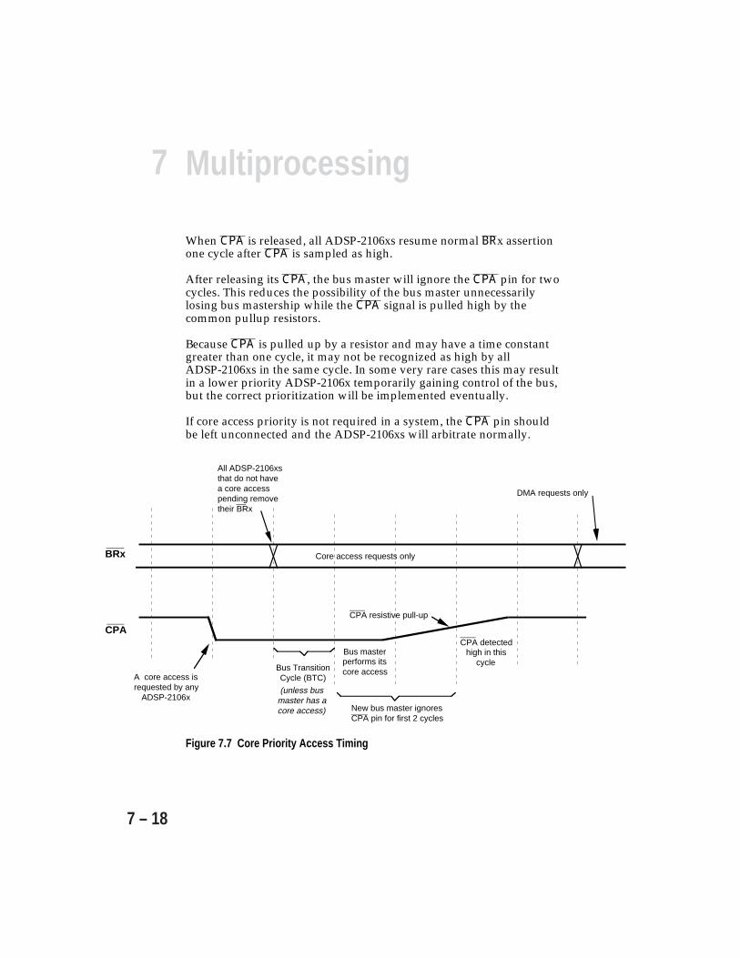
7 Multiprocessing
7 – 18
When CPA is released, all ADSP-2106xs resume normal BRx assertionone cycle after CPA is sampled as high.
After releasing its CPA, the bus master will ignore the CPA pin for twocycles. This reduces the possibility of the bus master unnecessarilylosing bus mastership while the CPA signal is pulled high by thecommon pullup resistors.
Because CPA is pulled up by a resistor and may have a time constantgreater than one cycle, it may not be recognized as high by allADSP-2106xs in the same cycle. In some very rare cases this may resultin a lower priority ADSP-2106x temporarily gaining control of the bus,but the correct prioritization will be implemented eventually.
If core access priority is not required in a system, the CPA pin shouldbe left unconnected and the ADSP-2106xs will arbitrate normally.
Figure 7.7 Core Priority Access Timing
Bus Transition Cycle (BTC)
CPA
BRx Core access requests only
A core access is requested by any
ADSP-2106x
DMA requests only
Bus master performs its core access
All ADSP-2106xs that do not have a core access pending remove their BRx
CPA resistive pull-up
CPA detected high in this
cycle
New bus master ignores CPA pin for first 2 cycles
(unless bus master has a core access)
7Multiprocessing
7 – 19
7.3.5 Bus Synchronization After ResetWhen a multiprocessing system is reset by the RESET pin, the busarbitration logic on each processor must synchronize to insure that onlyone ADSP-2106x will drive the external bus. One ADSP-2106x mustbecome the bus master, and all other processors must recognize which oneit is before actively arbitrating for the bus. The bus synchronizationscheme also allows the system to safely bring individual ADSP-2106xsinto and out of reset.
A soft reset (SRST) does not resynchronize ADSP-21062 silicon revision 1.xparts or ADSP-21060/62 silicon revision 2.x (or later) parts.
Note that a soft reset (SRST) does resynchronize ADSP-21062 siliconrevision 0.x parts and ADSP-21060 silicon revision 1.x parts.
One of the ADSP-2106xs in the system must be assigned ID=001 in orderfor the bus synchronization scheme to function properly. This processoralso holds the external bus control lines stable during reset. Bus arbitrationsynchronization is disabled if the ADSP-2106x is in a single-processorsystem (ID=000).
To synchronize their bus arbitration logic and define the bus master after asystem reset, the multiple ADSP-2106xs obey the following rules:
• All ADSP-2106xs except the one with ID=001 will deassert their BRx lineduring reset. They will keep their BRx deasserted for at least two cyclesafter reset and until their bus arbitration logic is synchronized.
• After reset, an ADSP-2106x will consider itself synchronized when it sees acycle in which only one BRx line is asserted. The ADSP-2106x will identifythe bus master by recognizing which BRx is asserted, and will update itsinternal record of who the current master is (in the current bus master field,CRBM, of the SYSTAT register).
• The ADSP-2106x with ID=001 will assert its BRx (BR1) during reset and forat least two cycles after reset. If no other BRx lines are asserted during thesecycles, the ADSP-2106x with ID=001 will drive the memory control signalsto prevent them from glitching. (Although it is asserting its BRx anddriving the memory control signals during these cycles, this processor doesnot perform reads or writes over the bus.)
If the ADSP-2106x with ID=001 is synchronized by the end of the twocycles following reset, it becomes the bus master. If it is not synchronized atthis time, it will deassert its BRx (BR1) and wait until it is.
7 Multiprocessing
7 – 20
When an ADSP-2106x has synchronized itself, it sets the BSYN bit inthe SYSTAT register.
If one ADSP-2106x comes out of reset after the others havesynchronized and started program execution, that processor may notbe able to synchronize immediately (e.g. if it sees more than one BRxline asserted). If the unsynchronized processor tries to execute aninstruction with an off-chip read or write, it cannot assert its BRx lineto request the bus and execution is delayed until it can synchronizeand correctly arbitrate for the bus.
Synchronization cannot occur while HBG is asserted, because busarbitration is suspended while the bus is controlled by a host. If HBR isasserted immediately after reset and no bus arbitration has taken place,the ADSP-2106x with ID=001 is considered to be the last bus master.
As mentioned above, the ADSP-2106x with ID=001 maintains correctlogic levels on the RD, WR, MS3-0, PAGE, and HBG signals duringreset.
Because the “001” processor can be accidently reset by an erroneouswrite to the soft reset bit (SRST) of the SYSCON register, it behaves inthe following manner during reset:
• While it is in reset, the ADSP-2106x with ID=001 attempts to gaincontrol of the bus by asserting BR1.
• While it is in reset, the ADSP-2106x with ID=001 will drive the RD,WR, MS3-0, DMAG1, DMAG2, PAGE, and HBG signals only if itdetermines that it has control of the bus. For the processor to decideit has control of the bus, two conditions must be true: 1) BR1 wasasserted and no other BRx lines were asserted in the previous cycle,and 2) HBG was deasserted in the previous cycle.
The ADSP-2106x with ID=001 will continue to drive the RD, WR,MS3-0, DMAG1, DMAG2, PAGE, and HBG signals for two cycles afterreset, as long as neither HBG nor any other BRx lines are asserted. Atthe end of the second cycle it assumes bus mastership (if it issynchronized), and normal bus arbitration begins in the followingcycle. If it is not synchronized, it deasserts BR1, stops driving thememory control signals, and does not arbitrate for the bus until itbecomes synchronized.

7Multiprocessing
7 – 21
Although the bus synchronization scheme allows individualprocessors to be reset, the ADSP-2106x with ID=001 may fail to drivethe memory control signals if it is in reset while any other processorsare asserting their BRx line.
If the ADSP-2106x with ID=001 has asserted HBG while it is in reset, itwill be synchronized when RESET is deasserted. This allows the hostto start using the bus while the ADSP-2106xs are still in reset.
If a host processor attempts to reset the ADSP-2106x bus master (whichis driving the HBG output), the host will immediately lose control ofthe bus.
During reset, the ACK line is pulled high internally by the ADSP-2106xbus master (with a 2 kΩ equivalent resistor).
7.4 SLAVE DIRECT READS & WRITESThe ADSP-2106x bus master can directly access the internal memoryand IOP registers of a slave ADSP-2106x by simply reading or writingto the appropriate address in multiprocessor memory space—this iscalled a direct read or direct write. Each ADSP-2106x bus slave monitorsaddresses driven on the external bus and responds to any that fallwithin its region of multiprocessor memory space.
These accesses are invisible to the slave ADSP-2106x’s core processorbecause they are performed through the external port and via theon-chip I/O bus—not the DM bus or PM bus. (See Figure 8.1 in theHost Interface chapter.)
This is an important distinction, because it allows the slave’s coreprocessor to continue program execution uninterrupted.
The ADSP-2106x bus master can directly read and write the slave’sIOP registers to send a vector interrupt, for example, or to set up aDMA transfer.
To read or write 48-bit instruction words, the IWT (Instruction WordTransfer) bit of the SYSCON register must be set to 1. To read or write32-bit data words, the IWT bit must be cleared to 0. When this bit is set,it overrides the IMDWx (Internal Memory Data Width) bit of eachmemory block.

7 Multiprocessing
7 – 22
For heavily loaded buses, or when external data buffers are used, asingle wait state can be added to all multiprocessor memory accesses.This option is selected by the MMSWS bit of the WAIT register.
7.4.1 Direct WritesWhen a direct write to a slave ADSP-2106x occurs, the address anddata are latched on-chip by the I/O processor. The I/O processorbuffers the address and data in a special set of FIFO buffers. Ifadditional direct writes are attempted when the FIFO buffer is full, theslave ADSP-2106x deasserts its ACK line until the buffer is no longerfull. Up to six direct writes can be performed before another is delayed.(The direct write buffer itself may be held off for up to four cycles if allof the serial port DMA channels are active or for up to nine cycles perchain if DMA chaining is occurring.)
7.4.1.1 Direct Write LatencyWhen data is written to an ADSP-2106x bus slave, the data andaddress are latched at the I/O pins in a four-level FIFO buffer; thisbuffer is called the slave write FIFO (see again Figure 8.1 in theHost Interface chapter). In the following cycle, the slave write FIFOattempts to complete the write internally. This allows the masterADSP-2106x to perform writes at the full clock rate. The slave writeFIFO cannot be explicitly read by the slave ADSP-2106x’s coreprocessor, nor can its status be determined.
Writes to the IOP registers will usually occur in the following one ortwo cycles, or when any current DMA transfer is completed. The writewill take more than two cycles only if a direct write in the previouscycle was held off by a full buffer.
If the buffer is full when a write is attempted, the slave ADSP-2106xwill deassert its ACK line until the buffer is not full. The buffer willusually flush out within one cycle, thus creating a write latency, unlesshigher priority on-chip DMA transfers are occurring.
Slave reads will be held off when there is data in the write FIFO—thisprevents false data reads and out-of-sequence operations.
7Multiprocessing
7 – 23
The DWPD (Direct Write Pending) bit of the SYSTAT register indicateswhen a direct write to internal memory is pending in the I/Oprocessor’s direct write FIFO or data is pending in the slave write FIFO(at the external port I/O pins). Direct writes and IOP register accessesmay be completed in different sequences. If, for example, theADSP-2106x master performs a direct memory write and then writes toan IOP register on a slave, the IOP register write may complete beforethe direct write.
7.4.2 Direct ReadsWhen a direct read of a slave ADSP-2106x occurs, the address islatched on-chip by the I/O processor and ACK is deasserted. When thecorresponding location in memory is read internally, the ADSP-2106xdrives the data off-chip and asserts its ACK line. Direct reads cannot bepipelined like direct writes—they only occur one at a time.
Note that while direct writes have a maximum pipelined throughputof one per cycle, direct reads have a maximum throughput of one perevery two cycles (for synchronous IOP register reads) or one per everyfour cycles (for synchronous internal memory reads). See Table 11.5,“Data Delays & Throughputs”, in Chapter 11. Because of this lowbandwidth, direct reads are not the most efficient method oftransferring data out of a slave ADSP-2106x—setting up a mastermode DMA channel on the slave to perform writes is more efficient,although it requires additional programming. The advantage of directreads is that no programming of the DMA controller is required.
7.4.3 Broadcast WritesBroadcast writes allow simultaneous transmission of data to all of theADSP-2106xs in a multiprocessing system. The master ADSP-2106xcan perform broadcast writes to the same memory location or IOPregister on all of the slaves. During broadcast writes, the master alsowrites to itself unless the broadcast is a DMA write. Broadcast writescan be used to implement reflective semaphores in a multiprocessingsystem (see “Bus Lock & Semaphores” later in this chapter). Broadcastwrites can also be used to simultaneously download code or data tomultiple processors.
The highest region of multiprocessor memory space, addresses0x0038 0000 to 0x003F FFFF, is used for broadcast writes. When a writeaddress falls within this region, each ADSP-2106x slave responds byaccepting the access; the master ADSP-2106x also accepts its ownbroadcast write. A read cycle generated in the broadcast write regionreads the corresponding location in that processor’s internal memoryand does not assert the processor’s BRx.
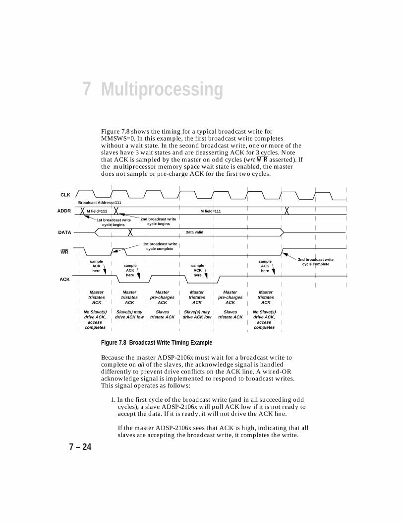
7 Multiprocessing
7 – 24
Figure 7.8 shows the timing for a typical broadcast write forMMSWS=0. In this example, the first broadcast write completeswithout a wait state. In the second broadcast write, one or more of theslaves have 3 wait states and are deasserting ACK for 3 cycles. Notethat ACK is sampled by the master on odd cycles (wrt WR asserted). Ifthe multiprocessor memory space wait state is enabled, the masterdoes not sample or pre-charge ACK for the first two cycles.
CLK
ADDR
WR
Broadcast Address=111
M field=111
Data validDATA
2nd broadcast writecycle begins
1st broadcast writecycle complete
2nd broadcast writecycle complete
ACK
sample ACKhere
Mastertristates
ACK
Masterpre-charges
ACK
Mastertristates
ACK
Slave(s) maydrive ACK low
Slavestristate ACK
No Slave(s)drive ACK,
access completes
1st broadcast writecycle begins
sample ACKhere
sample ACKhere
sample ACKhere
M field=111
Mastertristates
ACK
Slave(s) maydrive ACK low
Masterpre-charges
ACK
Slavestristate ACK
Mastertristates
ACK
No Slave(s)drive ACK,
access completes
Figure 7.8 Broadcast Write Timing Example
Because the master ADSP-2106x must wait for a broadcast write tocomplete on all of the slaves, the acknowledge signal is handleddifferently to prevent drive conflicts on the ACK line. A wired-ORacknowledge signal is implemented to respond to broadcast writes.This signal operates as follows:
1. In the first cycle of the broadcast write (and in all succeeding oddcycles), a slave ADSP-2106x will pull ACK low if it is not ready toaccept the data. If it is ready, it will not drive the ACK line.
If the master ADSP-2106x sees that ACK is high, indicating that allslaves are accepting the broadcast write, it completes the write.
7Multiprocessing
7 – 25
2. During all succeeding even cycles in which the broadcast write is notfinished, the slave ADSP-2106xs will not drive ACK. Instead, themaster ADSP-2106x drives (i.e. pre-charges) ACK high and mustcontinue the write. (Go to Step 1.)
In most cases the ACK signal will be high and the ADSP-2106x slaveswill be ready to accept data at the start of the broadcast write—thewrite completes in one cycle. If the ACK signal is low, however, or oneof the slaves is not ready to accept the data, the broadcast write willtake a minimum of three cycles.
When the wait state for multiprocessor memory space is enabled (withthe MMSWS bit of the WAIT register), none of the ADSP-2106xs willdrive ACK in the first cycle, the master pre-charges ACK in the secondcycle, and the slaves may drive ACK in the third cycle. In this case thebroadcast write will again take a minimum of three cycles to complete.
(Note: The ADSP-2106x bus master enables a keeper latch on the ACKline to prevent the signal from drifting. This eliminates any powerconsumption caused by the signal drifting to the switching point andimproves the robustness of broadcast writes. Multiprocessor systemsthat use broadcast writes should keep the ACK signal line as free ofnoise as possible.)
7.4.4 Shadow Write FIFOBecause the ADSP-2106x’s internal memory must operate at highspeeds, writes to the memory do not go directly into the memoryarray, but rather to a two-deep FIFO called the shadow write FIFO.
When an internal memory write cycle occurs, data in the FIFO fromthe previous write is loaded into memory and the new data goes intothe FIFO. This operation is normally transparent, since any reads of thelast two locations written are intercepted and routed to the FIFO.There is only one case in which you need to be aware of the shadowwrite FIFO: mixing 48-bit and 32-bit word accesses to the samelocations in memory.
The shadow FIFO cannot differentiate between the mapping of 48-bitwords and mapping of 32-bit words. (See Figures 5.8 and 5.9 in theMemory chapter.) Thus if you write a 48-bit word to memory and thentry to read the data with a 32-bit word access, the shadow FIFO willnot intercept the read and incorrect data will be returned.
7 Multiprocessing
7 – 26
If 48-bit accesses and 32-bit accesses to the same locations absolutelymust be mixed in this way, you must flush out the shadow FIFO withtwo dummy writes before attempting to read the data.
7.5 DATA TRANSFERS THROUGH THE EPBx BUFFERSIn addition to direct reads and writes, the ADSP-2106x bus master cantransfer data to and from the slave ADSP-2106xs through the externalport FIFO buffers, EPB0, EPB1, EPB2, and EPB3. Each of these buffers,which are part of the IOP register set, is a six-location FIFO. Bothsingle-word transfers and DMA transfers can be performed throughthe EPBx buffers. DMA transfers are handled internally by theADSP-2106x’s DMA controller, but single-word transfers must behandled by the ADSP-2106x core.
Each EPBx buffer has a read port and a write port, both of which canconnect internally to either the EPD (External Port Data) bus or to alocal bus which in turn can connect to the IOD (I/O Data) bus, PMData bus, or DM Data bus. This is shown in Figure 8.1 in theHost Interface chapter. Note that direct reads and writes bypass theEPBx buffers and go directly to internal memory.
7.5.1 Single-Word TransfersWhen the ADSP-2106x master writes a single data word to a slave’sEPBx buffers, the slave core’s program must read the data. Conversely,when the slave’s core writes a single piece of data to one of its EPBxbuffers, the master must perform an external bus read cycle to obtainit. Because the EPBx buffers are six-deep FIFOs (in both directions), themaster and the slave’s core are allowed extra time to read the data—efficient, continuous, single-word transfers can thus be performed inreal-time, with low latency and without using DMA.
If the ADSP-2106x master attempts a read from an empty EPBx bufferon a slave, the access will be held off with the ACK signal until thebuffer receives data from the slave’s core. If the slave’s core attempts towrite to a full EPBx buffer, the access is also delayed and the core willhang until the buffer is externally read by the master. To prevent thisfrom happening, the BHD (Buffer Hang Disable) bit should be set to 1in the SYSCON register. The full or empty status of a particular EPBxbuffer can be determined by reading the appropriate DMACx control/status register.

7Multiprocessing
7 – 27
Similarly, if the ADSP-2106x master attempts a write to a full EPBxbuffer on a slave, the access will be held off with ACK until the bufferis read by the slave’s core. If the slave’s core attempts to read from anempty buffer, the access is also held off and the core will hang until thebuffer is externally written from the bus master. The BHD bit can alsobe used to prevent a hang condition in this case.
Each EPBx buffer can be flushed (i.e. cleared) by writing a 1 to theFLSH bit in the corresponding DMACx control register. This bit is notlatched internally and will always be read as a 0. Status can change inthe following cycle. An EPBx buffer should not be enabled and flushedin the same cycle.
Note: To perform single-word, non-DMA transfers through the EPBxbuffers, the DMA enable bit (DEN) must be cleared in the appropriateDMACx control register.
7.5.1.1 Interrupts For Single-Word TransfersThe interrupts for the four external port DMA channels can be used tocontrol single-word data transfers between the ADSP-2106x bus masterand a slave. To do this, the DMACx control register must have thefollowing bit settings: DEN=0 and INTIO=1. This disables DMA(DEN=0) and enables interrupt-driven I/O (INTIO=1). See the DMAchapter or Control/Status Registers appendix of this manual for acomplete description of the DMACx control registers.
In this case the interrupt is generated whenever data becomes availablein the read port of the EPBx buffer, or whenever the write port doesnot have new data to transmit. The EPBx buffer can then be read orwritten, either internally by the ADSP-2106x slave’s core or externallyby the master. Generating interrupts in this fashion is useful forimplementing interrupt-driven I/O controlled by the ADSP-2106x coreprocessor.
This interrupt may be masked out (i.e. disabled) in the IMASK register.If the interrupt is later enabled in IMASK, the corresponding IRPTLlatch bit must be cleared to clear any interrupt request that may haveoccurred.
7 Multiprocessing
7 – 28
7.5.2 DMA TransfersThe ADSP-2106x bus master can also set up DMA transfers to andfrom a slave ADSP-2106x. The master can write to the slave’s DMAcontrol and parameter registers to set up an external port DMAoperation. This is the most efficient way to transfer blocks of databetween two ADSP-2106xs.
• DMA Transfers to Internal Memory. The ADSP-2106x master can setup external port DMA channels to transfer data to and from a slave’sinternal memory.
• DMA Transfers to External Memory. The ADSP-2106x master can setup an external port DMA channel to transfer data directly to externalmemory using the DMA request and grant lines (DMARx, DMAGx).
Refer to the DMA chapter of this manual for details on setting up DMAoperations. Figure 6.9 in the “System Configurations For ADSP-2106xInterprocessor DMA” section of the DMA chapter shows the differentways you can set up external port DMA transfers between twoADSP-2106xs, as well as the advantages and disadvantages of each.
7.5.2.1 DMA Transfers To Internal MemoryThe ADSP-2106x master can set up external port DMA channels totransfer blocks of data to and from a slave’s internal memory. To setup the DMA transfer, the master must initialize the slave’s control andparameter registers for that channel. Once the DMA channel is set up,the master may simply read from (or write to) the corresponding EPBxbuffer on the slave, or it may set up its own DMA controller to performthe transfers. If the slave’s buffer is empty (or full), the access isextended until data is available (or stored). This method allows fastand efficient data transfers.
Packing and unpacking of DMA data words is selected by the PMODEbits in the external port DMA control registers (DMAC6, DMAC7,DMAC8, and DMAC9). Either 16-to-32, 16-to-48, or 32-to-48 bitpacking/unpacking can be selected.
The ADSP-2106x master may also use the DMARx/DMAGxhandshake signals to control a DMA transfer, but not when a hostprocessor has gained control of the bus.
7Multiprocessing
7 – 29
7.5.2.2 DMA Transfers To External MemoryThe ADSP-2106x’s DMA controller can also be used to transfer datadirectly to external memory. The external handshake mode for externalport DMA channel 7 or 8 will provide the DMARx/DMAGxhandshaking for this type of transfer. Again, this is not possible whena host processor has gained control of the bus.
7.6 BUS LOCK & SEMAPHORESSemaphores can be used in multiprocessor systems to allow theprocessors to share resources such as memory or I/O. A semaphore isa flag that can be read and written by any of the processors sharing theresource. The value of the semaphore tells the processor when it canaccess the resource. Semaphores are also useful for synchronizing thetasks being performed by different processors in a multiprocessingsystem.
With the use of its bus lock feature, the ADSP-2106x has the ability toread and modify a semaphore in a single indivisible operation—a keyrequirement of multiprocessing systems.
Because both external memory and each ADSP-2106x’s internalmemory (and IOP registers) are accessible by every other ADSP-2106x,semaphores can be located almost anywhere. Read-modify-writeoperations on semaphores can be performed if all of the ADSP-2106xsobey two simple rules:
1. An ADSP-2106x must not write to a semaphore unless it is the busmaster. This is especially important if the semaphore is located inthe ADSP-2106x’s own internal memory or IOP registers.
2. When attempting a read-modify-write operation on a semaphore,the ADSP-2106x must have bus mastership for the duration of theoperation.
Both of these rules are adhered to when an ADSP-2106x uses its buslock feature, which “locks in” its mastership of the bus and preventsthe other processors from simultaneously accessing the semaphore.
7 Multiprocessing
7 – 30
Bus lock is requested by setting the BUSLK bit in the MODE2 register.When this happens, the ADSP-2106x initiates the bus arbitrationprocess in the usual fashion, by asserting its BRx line. When it becomesbus master, it locks the bus (i.e. retains bus mastership) by keeping itsBRx line asserted even when it is not performing an external read orwrite. Host bus request (HBR) is also ignored during a bus lock. Whenthe BUSLK bit is cleared, the ADSP-2106x gives up the bus bydeasserting its BRx line.
While the BUSLK bit is set, the ADSP-2106x can determine if it hasacquired bus mastership by executing a conditional instruction withthe BM or NOT BM condition codes, for example:
IF NOT BM JUMP(PC,0); /* wait for bus mastership */
If it has become the bus master, the ADSP-2106x can proceed with theexternal read or write. If not, it can clear its BUSLK bit and try againlater.
A read-modify-write operation is accomplished with the following steps:
1. Request bus lock by setting the BUSLK bit in MODE2.2. Wait for bus mastership to be acquired.3. Wait until Direct Write Pending (DWPD) is zero.4. Read the semaphore, test it, and then write to it.
Locking the bus prevents other processors from writing to thesemaphore while the read-modify-write is occurring. (Note: If thesemaphore is reflective, located in the ADSP-2106x’s internal memoryor an IOP register, the processor must write to it only when it has buslock.) After bus mastership is aquired, the Direct Write Pending statusin SYSTAT must be checked to ensure that a semaphore write byanother processor is not pending.
Bus lock can be used in combination with broadcast writes toimplement reflective semaphores in a multiprocessing system. Thereflective semaphore should be located at the same address in internalmemory (or IOP register) of each ADSP-2106x. To check thesemaphore, each ADSP-2106x simply reads from its own internalmemory. To modify the semaphore, an ADSP-2106x requests bus lockand then performs a broadcast write to the semaphore address onevery ADSP-2106x, including itself. Before modifying the semaphore,though, the ADSP-2106x must re-check it to verify that anotherprocessor has not changed it. With reflective semaphores, the externalbus is used only for updating the semaphore, not for reading it. Thisgreatly reduces bus traffic.
7Multiprocessing
7 – 31
7.6.1 Example: Sharing A DMA Channel With Reflective SemaphoresA single DMA channel can be shared by more than one ADSP-2106xby using the channel’s control register as a reflective semaphore. TheDMA channel control register is a memory-mapped IOP register oneach ADSP-2106x. If the control register is equal to zero, the channel isdisabled and is not being used by any processor. If the control registeris non-zero, the DMA channel is in use.
Before an ADSP-2106x can use the DMA channel, it must read thesemaphore to determine if the channel is in use. If not, the ADSP-2106xcan request bus lock and then execute a read-modify-write operationto set the semaphore on each of the processors sharing the DMAchannel. Before performing the read-modify-write, though, theADSP-2106x should recheck the semaphore to assure that the DMAchannel is still free. Once this is done, the ADSP-2106x should clear theBUSLK bit to unlock the bus and can proceed with the DMAtransfer(s). When the transfer(s) are completed, this ADSP-2106x mustclear the semaphore to tell the other processors that the channel isavailable for use.
The following code performs the read-modify-write operationdescribed above:
#define semaphore 0x0038001C /* Broadcast write to *//* DMAC6 control register *//* on all ADSP-2106xs. */
...
BIT SET MODE2 BUSLK; /* Request bus lock */IF NOT BM JUMP(PC,0); /* Wait for bus mastership */USTAT1=DM(SYSTAT); /* Check Direct Write Pending */BIT TST USTAT1 0X1000; /* Status to ensure no
writes happen */IF NE JUMP (PC,-2); /* After bus lock */R0=DM(semaphore); /* Read semaphore */R0=PASS RO /* Set condition codes */
IF NE JUMP(PC,3); /* Test semaphore - don’t write if resource is unavailable.*/
R0=R0+1; /* Modify semaphore */DM(semaphore)=R0; /* Write semaphore */BIT CLR MODE2 BUSLK; /* Release bus lock */
Notes:1.) The IF NOT BM JUMP(PC,0) instruction through the IF NE JUMP (PC, -2)
instruction is only necessary for internal semaphores.2.) The R0=DM(semaphore) instruction will not be executed until bus mastership is
acquired and locked.3.) The DM(semaphore)=R0 instruction is a broadcast write.
7 Multiprocessing
7 – 32
7.7 INTERPROCESSOR MESSAGES & VECTOR INTERRUPTSThe ADSP-2106x bus master can communicate with slaveADSP-2106xs by writing messages to their IOP registers. TheMSGR0-MSGR7 registers are general-purpose registers which can beused for convenient message passing between ADSP-2106xs. They arealso useful for semaphores and resource sharing between multipleADSP-2106xs. The MSGRx and VIRPT registers can be used formessage passing in the following ways:
• Message Passing. The master ADSP-2106x can communicate with aslave ADSP-2106x by writing and/or reading any of the 8 messageregisters, MSGR0–MSGR7, on the slave.
• Vector Interrupts. The master ADSP-2106x can issue a vector interruptto a slave by writing the address of an interrupt service routine to theslave’s VIRPT register. This causes an immediate high-priority interrupton the slave which, when serviced, will cause it to branch to thespecified service routine.
The MSGRx and VIRPT registers also support the host processorinterface. Since these registers may be shared resources within a singleADSP-2106x, conflicts may occur—your system software must preventthis. For further discussion of IOP register access conflicts, refer to theControl/Status Registers appendix of this manual.
7.7.1 Message Passing (MSGRx)There are three methods by which the ADSP-2106x bus master cancommunicate with a slave through the MSGRx message registers:1) vector-interrupt-driven, 2) register handshake, and 3) register write-back.
For the vector-interrupt-driven method, the master fills predeterminedMSGRx registers on the slave with data and triggers a vector interruptby writing the address of the service routine to the slave’s VIRPTregister. The slave’s service routine should read the data from theMSGRx registers and then write “0” into VIRPT to tell the master it isdone. The service routine could also use one of the slave’s FLAG3-0pins to tell the master it has finished.
For the register handshake method, four of the MSGRx registers shouldbe designated as follows: a receive register (R), a receive handshakeregister (RH), a transmit register (T), and a transmit handshake register(TH). To pass data to the slave ADSP-2106x, the master would writedata into T and then write a “1” into TH. When the slave sees a “1” inTH, it reads the data from T and then writes back a “0” into TH. When
7Multiprocessing
7 – 33
the master sees a “0” in TH, it knows that the transfer is complete. Asimilar sequence of events occurs when the slave passes data to themaster through R and RH.
The register write-back method is similar to register handshaking, butuses only the T and R data registers. The master writes data to T. Whenthe slave sees a non-zero value in T, it retrieves it and writes back a “0”to T. A similar sequence occurs when the master is receiving data. Thissimpler method works well as long as the data to be passed does notinclude “0.”
7.7.2 Vector Interrupts (VIRPT)Vector interrupts are used for interprocessor commands between twoADSP-2106xs or between a host and the ADSP-2106x. When theexternal processor writes an address to the ADSP-2106x’s VIRPTregister, a vector interrupt is caused.
When the vector interrupt is serviced, the ADSP-2106x automaticallypushes the status stack and begins executing the service routinelocated at the address specified in VIRPT. The lower 24 bits of VIRPTcontain the address; the upper 8 bits may be optionally used as data tobe read by the interrupt service routine. At reset, VIRPT is initialized toits standard address in the ADSP-2106x’s interrupt vector table.
The minimum latency for vector interrupts is six cycles, five of whichare NOPs. When the RTI (return from interrupt) instruction is reachedin the service routine, the ADSP-2106x automatically pops the statusstack.
The VIPD bit in the SYSTAT register reflects the status of the VIRPTregister. If VIRPT is written while a previous vector interrupt ispending, the new vector address replaces the pending one. If VIRPT iswritten while a previous vector interrupt is being serviced, the newvector address is ignored and no new interrupt is triggered. If theADSP-2106x writes to its own VIRPT register it is ignored.
To use the slave ADSP-2106x’s vector interrupt feature, the masterADSP-2106x should perform the following sequence of actions:
1. Poll the slave’s VIRPT register until it reads a certain token value(i.e. zero).
2. Write the vector interrupt service routine address to VIRPT.3. When the service routine is finished, the slave ADSP-2106x should
write the token back into VIRPT to indicate that it is finished andthat another vector interrupt can be initiated.
7 Multiprocessing
7 – 34
The DWPD (Direct Write Pending) bit of the SYSTAT register indicateswhen a direct write to internal memory is pending. Pending directwrites may occur in different sequences. If, for example, the masterADSP-2106x performs a direct write to a slave and then writes to anIOP register on the slave, the IOP register write may complete beforethe direct write. Because of this, direct writes performed just beforevector interrupt writes (to VIRPT) may be delayed until after thebranch to the interrupt vector:
1. The master ADSP-2106x performs a direct write to the internalmemory of a slave.
2. The master ADSP-2106x writes to the VIRPT register of the slave toinitiate a vector interrupt. This causes the direct write to be delayed.
3. The slave ADSP-2106x jumps to the vector interrupt service routine.4. The direct write is completed after the interrupt service routine is
underway.
To prevent this from happening, the master ADSP-2106x should checkthat all direct writes have completed before writing to the slave’sVIRPT register. This can be done by polling the slave’s DWPD bit (inSYSTAT) after performing a direct write, waiting for it to becomecleared, and then proceeding with the write to VIRPT.
7.8 SYSTAT REGISTER STATUS BITSThe SYSTAT register provides status information, primarily formultiprocessor systems. Table 7.4 shows the status bits in this register.
Bit(s)Name DefinitionHSTM Host MastershipBSYN Bus SynchronizationCRBM Current Bus Master (ID2-0 of ADSP-2106x bus master)IDC ID Code (ID2-0 of this ADSP-2106x)DWPD Direct Write PendingVIPD Vector Interrupt PendingHPS Host Packing Status
Table 7.4 SYSTAT Status Bits

7Multiprocessing
7 – 35
11 10 9 8 7 6 5 4 3 2 1 0
00000000
15 14 13 12
0000
26 25 24 23 22 21 20 19 18 17
000000000000
31 30 29 28 27
0000
16
HSTMHost Mastership
CRBMCurrent Bus Master
DWPDDirect Write Pending
HPSHost Packing Status00 = packing complete01 = first stage of all packing and unpacking modes10 = second stage of 16-to-48 bit packing/unpacking or 32-to-48 bit packing/unpacking
BSYNBus Synchronization
IDCID Code
VIPDVector Interrupt Pending
Figure 7.9 SYSTAT Register

7 Multiprocessing
7 – 36
HSTM Host Mastership. Indicates whether the host processor is has been grantedcontrol of the bus.
1=Host is bus master0=Host is not bus master
BSYN Bus Synchronization. Indicates when the ADSP-2106x’s bus arbitrationlogic is synchronized after reset. (See “Bus Synchronization After Reset.”)
1=Bus arbitration logic is synchronized0=Bus arbitration logic is not synchronized
CRBM Current Bus Master. Indicates the ID code of the ADSP-2106x that is thecurrent bus master. If CRBM is equal to the ID of this ADSP-2106x then it isthe current bus master. CRBM is only valid for ID2-0 > 0 (greater than zero).When ID2-0=000, CRBM is always 1.
IDC ID Code. Indicates the ID2-0 inputs of this ADSP-2106x.
DWPD Direct Write Pending. Indicates when a direct write to the ADSP-2106x’sinternal memory is pending. The DWPD bit is cleared when the direct writehas been completed. (Direct writes may be delayed for several cycles isDMA chaining is underway or if higher priority DMA requests occur.Maximum delay is 12 cycles.)
1=Direct write pending0=No direct write pending
VIPD Vector Interrupt Pending. Indicates that a pending vector interrupt has notyet been serviced. The VIPD bit is set when the VIRPT register is written toand is cleared upon return from the interrupt service routine. The masterADSP-2106x (or host processor) that issued the vector interrupt shouldmonitor this bit to determine when the service routine has been completed,and when a new vector interrupt may be issued.
1=Vector interrupt pending0=No vector interrupt pending
HPS Host Packing Status. Indicates when host word packing is completed or,if not, what stage of the process is taking place.
00=Packing complete01=1st stage of all packing and unpacking modes.10=2nd stage of 16-to-48 bit packing/unpacking or 32-to-48 bit packing/unpacking
8
8 – 1
Host Interface
8.1 OVERVIEWThe ADSP-2106x’s host interface allows easy connection to standardmicroprocessor buses, both 16-bit and 32-bit, with little additionalhardware required. The ADSP-2106x accommodates eithersynchronous or asynchronous data transfers, allowing the host to use adifferent clock frequency. Asynchronous transfers at speeds up to thefull clock rate of the processor are supported. The host accesses theADSP-2106x through its external port, via the external bus (DATA47-0and ADDR31-0). The host interface is memory-mapped into the unifiedaddress space of the ADSP-2106x. Figure 8.1 shows a block diagram ofthe external port, I/O processor, and FIFO data buffers, illustrating theon-chip data paths for host-driven transfers. The four external portDMA channels are available for use by the host—DMA transfers ofcode and data can be performed with low software overhead.
The host processor requests and controls the ADSP-2106x’s externalbus with the host bus request (HBR), host bus grant (HBG), and ready(REDY) signals. Once it has gained control of the bus, the host can candirectly read and write the internal memory of the ADSP-2106x. It canalso read and write to any of the ADSP-2106x’s IOP registers,including the EPBx FIFO buffers. The host uses certain IOP registers tocontrol and configure the ADSP-2106x, SYSCON and SYSTAT forexample, and to set up DMA transfers. DMA transfers are controlledby the ADSP-2106x’s on-chip DMA controller once they have been setup by the host (or by the ADSP-2106x core). In a multiprocessorsystem, the host can access the internal memory and IOP registers ofevery ADSP-2106x. Vector interrupts provide efficient execution ofhost commands.
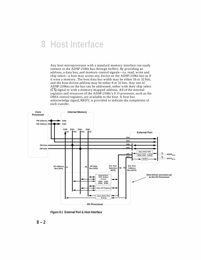
8 Host Interface
8 – 2
Any host microprocessor with a standard memory interface can easilyconnect to the ADSP-2106x bus through buffers. By providing anaddress, a data bus, and memory control signals—i.e. read, write andchip select—a host may access any device on the ADSP-2106x bus as ifit were a memory. The host data bus width may be either 16 or 32 bits,and the host-driven address may be either 8 or 32 bits. Any one ofADSP-2106xs on the bus can be addressed, either with their chip select(CS) signal or with a memory-mapped address. All of the internalregisters and resources of the ADSP-2106x’s I/O processor, such as theDMA control registers, are available to the host. A host busacknowledge signal, REDY, is provided to indicate the completion ofeach transfer.
External Port FIFO Buffers
Other IOP Registers
Direct Write FIFO
Ext. Port Data Bus
(EPD)
Slave Write FIFO(Async writes - 4 deep)(Sync writes - 2 deep)
Buffer
32
48
ADDR31-0
DATA47-0
External Port
Ext. Port Address
Bus (EPA)48 32
I/O Processor
Data Data Data
PM Data
DM Data
48
PM Address
DM Address
Addr
Addr
I/O Data Bus (IOD)
Addr
17I/O Address Bus (IOA)
PMD
Core Processor
Internal Memory
IODIOA DMD
PMA
DMA
PMD
DMD
EPD
EPA
Host-driven accesses go to the I/O Processor
(6-deep)
EPB0 EPB2EPB1 EPB3
(6-deep)
Figure 8.1 External Port & Host Interface

8Host Interface
8 – 3
Table 8.1 defines the ADSP-2106x pins used in host processorinterfacing.
Signal Type DefinitionHBR I/A Host Bus Request. Must be asserted by a host
processor to request control of the ADSP-2106x’sexternal bus. When HBR is asserted in amultiprocessing system, the ADSP-2106x that is busmaster will relinquish the bus and assert HBG. Torelinquish the bus, the ADSP-2106x places the address,data, select, and strobe lines in a high-impedance state.HBR has priority over all ADSP-2106x bus requests(BR1-6) in a multiprocessing system.
HBG I/O Host Bus Grant. Acknowledges an HBR bus request,indicating that the host processor may take control ofthe external bus. HBG is asserted (held low) by theADSP-2106x until HBR is released. In amultiprocessing system, HBG is output by theADSP-2106x bus master and is monitored by all others.
CS I/A Chip Select. Asserted by host processor to select theADSP 2106x.
REDY (o/d) O Host Bus Acknowledge. The ADSP-2106x deasserts REDY(low) to add wait states to an asynchronous access of itsinternal memory or IOP registers by a host. Open-drainoutput (o/d) by default; can be programmed in ADREDYbit of SYSCON register to be active drive (a/d). REDY willonly be output if the CS and HBR inputs are asserted.
SBTS I/S Suspend Bus Tristate. External devices can assertSBTS (low) to place the external bus address, data,selects, and strobes in a high-impedance state for thefollowing cycle. If the ADSP-2106x attempts to accessexternal memory while SBTS is asserted, the processorwill halt and the memory access will not be completeduntil SBTS is deasserted. SBTS should only be used torecover from PAGE faults or host processor/ADSP-2106x deadlock.
I=Input S=Synchronous (o/d)=Open DrainO=Output A=Asynchronous (a/d)=Active Drive
Table 8.1 Host Interface Signals

8 Host Interface
8 – 4
The following terms are used throughout this chapter, and are definedbelow for reference:
external bus DATA47-0, ADDR31-0, RD, WR, MS3-0, BMS,ADRCLK, PAGE, SW, ACK, and SBTS signals
multiprocessor system a system with multiple ADSP-2106xs, with orwithout a host processor; the ADSP-2106xs areconnected by the external bus and/or link ports
multiprocessor memory space portion of the ADSP-2106x’s memory map thatincludes the internal memory and IOP registersof each ADSP-2106x in a multiprocessingsystem; this address space is mapped into theunified address space of the ADSP-2106x
IOP register one of the control, status, or data buffer registersof the ADSP-2106x’s on-chip I/O processor
bus slave or slave mode an ADSP-2106x can be a bus slave to anotherADSP-2106x or to a host processor; theADSP-2106x becomes a “host bus slave” whenthe HBG signal is returned
bus transition cycle (BTC) a cycle in which control of the external bus ispassed from one ADSP-2106x to another (in amultiprocessor system)
host transition cycle (HTC) a cycle in which control of the external bus ispassed from the ADSP-2106x to the hostprocessor—during this cycle the ADSP-2106xstops driving the RD, WR, ADDR31-0, MS3-0,ADRCLK, PAGE, SW, and DMAGx signals,which must then be driven by the host
asynchronous transfers asynchronous host accesses of the ADSP-2106x;after acquiring control of the ADSP-2106x’sexternal bus, the host must assert the CS pin ofthe ADSP-2106x it wants to access
synchronous transfers synchronous host accesses of the ADSP-2106x;CS is not asserted and the host must act likeanother ADSP-2106x in a multiprocessor system,by generating an address in multiprocessormemory space, asserting SW and WR or RD,and driving out or latching in the data
8Host Interface
8 – 5
direct reads & writes a direct access of the ADSP-2106x’s internalmemory or IOP registers by anotherADSP-2106x or by a host processor
external port FIFO buffers EPB0, EPB1, EPB2, and EPB3—the IOP registersused for external port DMA transfers andsingle-word data transfers (from otherADSP-2106xs or from a host processor); thesebuffers are 6-deep FIFOs
single-word data transfers reads and writes to the EPBx external portbuffers, performed externally by the host orinternally by the ADSP-2106x core; these occurwhen DMA is disabled in the DMACx controlregister
DMACx control registers the DMA control registers for the EPBx externalport buffers: DMAC6, DMAC7, DMAC8, andDMAC9, corresponding respectively to EPB0,EPB1, EPB2, and EPB3 (see the DMA chapter orControl/Status Registers appendix of this manualfor a complete description of the DMACxcontrol registers)
8.2 HOST PROCESSOR CONTROL OF THE ADSP-2106XThe HBR and HBG signals allow a host processor to gain control of theADSP-2106x and its external bus. Once the host is granted control ofthe ADSP-2106x bus, it may transfer data either synchronously orasynchronously. Asynchronous transfers are most commonly used.The host bus may be 16, 32, or 48 bits wide for synchronous transfers,but only 16 or 32 bits wide for asynchronous transfers.
Data written to and read from the ADSP-2106x can be packed orunpacked into different word widths. When the width of the host busis 16 bits, data can be packed into 32-bit words or 48-bit words. Whenthe host bus is 32 bits wide, data can be packed into 48-bit words. Thehost packing mode control bits (HPM) in the SYSCON register areused to configure data packing and unpacking.
8 Host Interface
8 – 6
8.2.1 Acquiring The BusFor a host processor to gain access to the ADSP-2106x, it must firstassert HBR, the host bus request signal. HBR has priority over all BRxmultiprocessor bus requests, and when asserted will cause the currentADSP-2106x master to give up the bus to the host as soon as it hasfinished the current bus cycle.
The current ADSP-2106x bus master signals that it is transferringownership of the bus by asserting HBG (low) as soon as the currentbus operation has completed. The cycle in which control of the bus istransferred is called a host transition cycle (HTC).
Figure 8.2 shows the timing for bus acquisition by the host. HBG isasserted during the ADSP-2106x’s bus transition cycle (BTC) andremains asserted until HBR is deasserted by the host. (The bustransition cycle (BTC) shown in Figure 8.2 is the same as that of aSHARC-to-SHARC multiprocessor BTC, as described in Chapter 7,Multiprocessing. HBG freezes ADSP-2106x multiprocessor busarbitration during the time that the host owns the bus. (HBG shouldalso be used to enable the host’s signal buffers, as shown in Figure 8.8at the end of this chapter.) While HBG is asserted, the ADSP-2106xswill continue to assert and deassert their BRx lines as in normaloperation, but no BTCs will occur. The current ADSP-2106x bus masterwill keep its BRx asserted throughout the entire time the host controlsthe bus.
Once the host has gained control of the bus, it can choose to performeither synchronous or asynchronous transfers with the ADSP-2106x(s).To initiate asynchronous transfers, the host asserts (low) the CS pin ofthe ADSP-2106x that it intends to access and performs the read orwrite. (CS is ignored when HBG is not asserted.) To initiatesynchronous transfers, the host keeps all ADSP-2106x CS pinsdeasserted (high) and reads or writes to the ADSP-2106xs’multiprocessor memory space (just as one ADSP-2106x reads or writes toanother ADSP-2106x).
The host is responsible for driving the following signals during theHTC in which it gains control of the bus: ADDR31-0, RD, WR, SW, andPAGE. See Figure 8.3. These signals must also continue to be driven forthe entire time the host has the bus. In addition, the MS3-0, ADRCLK,DMAG1, and DMAG2 lines must be driven or weakly pulled up ordown—the ADSP-2106x bus master tristates these lines to allow thehost the possibility of using them.
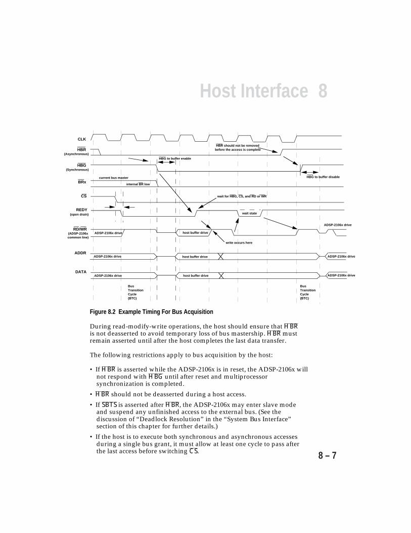
8Host Interface
8 – 7
current bus master
(ADSP-2106xcommon line)
CLK
HBR(Asynchronous)
HBR should not be removedbefore the access is complete
HBG(Synchronous)
BRx
CS
REDY
HBG to buffer disable
HBG to buffer enable
internal BR low
wait for HBG, CS, and RD or WR
wait state
ADSP-2106x driveRD/WR
ADSP-2106x drive host buffer drive
write occurs here
ADSP-2106x driveADDR
ADSP-2106x drive host buffer drive
DATAADSP-2106x drive host buffer drive ADSP-2106x drive
BusTransitionCycle(BTC)
BusTransitionCycle(BTC)
(open drain)
Figure 8.2 Example Timing For Bus Acquisition
During read-modify-write operations, the host should ensure that HBRis not deasserted to avoid temporary loss of bus mastership. HBR mustremain asserted until after the host completes the last data transfer.
The following restrictions apply to bus acquisition by the host:
• If HBR is asserted while the ADSP-2106x is in reset, the ADSP-2106x willnot respond with HBG until after reset and multiprocessorsynchronization is completed.
• HBR should not be deasserted during a host access.
• If SBTS is asserted after HBR, the ADSP-2106x may enter slave modeand suspend any unfinished access to the external bus. (See thediscussion of “Deadlock Resolution” in the “System Bus Interface”section of this chapter for further details.)
• If the host is to execute both synchronous and asynchronous accessesduring a single bus grant, it must allow at least one cycle to pass afterthe last access before switching CS.

8 Host Interface
8 – 8
• Synchronous accesses may not be used in systems with only oneADSP-2106x (with ID2-0=000).
Once the host has finished its task, it can relinquish control of the busby deasserting HBR. The ADSP-2106x bus master responds bydeasserting HBG. In the next cycle, the ADSP-2106x bus master againassumes control of the bus and normal multiprocessor arbitrationresumes. The host should not deassert HBR until after it has completedits last data transfer with the ADSP-2106x.
8.2.2 Asynchronous TransfersTo initiate asynchronous transfers after acquiring control of theADSP-2106x’s external bus, the host must assert the CS pin of theADSP-2106x it wants to access. This informs the ADSP-2106x that itwill be transferring data asynchronously with the host. The host mustthen drive the address of the memory location or IOP register that itwants to access. To simplify the hardware requirements for externalinterface logic, only the address bits shown in Table 8.2 need to bedriven.
AddressBits * CommentsADDR7-0 Must be driven in all cases.ADDR16-8 Must be driven only if the S field indicates an internal memory access.ADDR18-17 S field**—Must be driven “00” for IOP register accesses, “01” for
internal memory accesses, or “1m” for short word accesses. and eitherADDR21-19 M field**—Must be driven “000” to prevent other non-selected
ADSP-2106xs on the bus from thinking that a synchronousmultiprocessor memory space access is occurring.
orADDR31-22 E field**—one of the lines 31-22 driven as “1”.
Table 8.2 Address Bits To Be Driven During Asynchronous Host Accesses
* Setup and hold times for these address lines are specified in the ADSP-2106x Data Sheet.** For a complete description of these address fields, see “ADSP-2106x Memory Map” in the Memory chapter of this manual.
Table 8.2 covers all cases, including multiprocessor systems, but feweraddress bits may need to be driven depending on the system. In asingle-ADSP-2106x system, the host need not drive the M addressfield.
8Host Interface
8 – 9
Host direct reads and writes can be performed with normal words(32-bit or 48-bit) or short words (16-bit). Short words are accessed if theS field of the address is “1m”, where “m” is the most significant bit ofthe short word address. Normal words are accessed if the S field is“01”. 48-bit words are accessed if the IWT bit in the SYSCON register isset to 1, selecting instruction word transfers.
When using asynchronous transfers and direct access to internalmemory is not required, the address supplied to the ADSP-2106x neednot be the full 32 bits. Only the lower 8 bits, ADDR7-0, need besupplied. The ADDR21-17 bits must be zeros and the ADDR31-22 bitsare ignored, or ADDR21-19 need not be driven if one of the ADDR31-22bits is a 1. See Table 8.2.
Asynchronous Write Clock RatesTo allow full speed asynchronous writes, data is latched at the I/Opins in a four-level FIFO buffer; this buffer is called the slave write FIFO(see Figure 8.1). This buffering allows previously written words to beresynchronized while a new word is being written, and allowsasynchronous writes to occur at up to the full clock rate of theADSP-2106x.
Broadcast WritesA host may broadcast write to several ADSP-2106xs by asserting eachof their CS pins. Each ADSP-2106x will accept the write as if it were theonly device being addressed. Because the REDY line is wire-ORed (ifconfigured as an open-drain output), it will only appear asserted whenall selected ADSP-2106xs are ready. (This is true only if REDY is notactively pulled up.) ACK is not active when CS is asserted.
Uniprocessor Host InterfaceTo eliminate the need for a host to drive the M field address lines(ADDR21-19) in systems with only one ADSP-2106x (ID2-0=000), thisADSP-2106x will not recognize synchronous accesses. The host mustdrive these address lines however, if the ADSP-2106x’s ID2-0 isanything other than 000. (Note that this removes the requirement thatCS be asserted before RD.) To account for buffer delays when samplingthe REDY signal, be careful to ensure that it is properly resynchronizedby the host.

8 Host Interface
8 – 10
8.2.2.1 Asynchronous Transfer TimingWhen a ADSP-2106x’s CS chip select is asserted (low), the selectedADSP-2106x immediately deasserts the REDY signal, with a delay ofapproximately 10 ns. Refer to the ADSP-2106x Data Sheet for timingexact specifications. (The REDY deassertion is activated from CS andnot from RD or WR because the host interface buffers for RD and WRmay not yet be enabled if HBG has not been asserted. CS can beasserted before or after HBR is asserted, but REDY will not bereasserted until after HBG has been asserted and a RD or WR strobehas been applied. This is true only if a RD or WR strobe is active whenHBG is asserted, otherwise it is determined by the tTRDYHG switchingcharacteristic specified in the “Multiprocessor Bus Request & Host BusRequest” timing section of the ADSP-2106x Data Sheet.)
REDY is asserted prior to the RD or WR being asserted and becomesdeasserted only if the ADSP-2106x is not ready for the read or write tocomplete—the only exception is when CS is first asserted. The REDYpin is an open-drain output to facilitate interfacing to common buses.It can be changed to an active-drive output by setting the ADREDY bitin the SYSCON register.
Figure 8.3 shows the timing of a host write cycle, discussed below,including details of data packing and unpacking. This timing assumesthe use of the example host interface hardware shown in Figure 8.8 atthe end of this chapter.
1. The host asserts the address. HBR and CS are decoded from the hostbus interface address comparator and need not be supplied directlyby the host. The selected ADSP-2106x deasserts REDY immediately.
2. The host asserts WR and drives data (according to the timingrequirements specified in the data sheet).
3. The selected ADSP-2106x asserts REDY when it is ready to acceptthe data. This occurs after the current bus master has completed itscurrent transfer and has asserted HBG. HBG enables the hostinterface buffers to drive onto the ADSP-2106x bus.
4. The host deasserts WR when REDY is high and stops driving data.5. The selected ADSP-2106x latches data on the rising edge of WR.

8Host Interface
8 – 11
HBR
HostAddress
CS
Host buffersturn on
valid address valid
HBG
Driven by Host
Driven by ADSP-2106x Bus Master
DATA
BRx
ACK
REDYdata setup
valid
BusTransition
Cycle(BTC)
HostTransition
Cycle(HTC)
REDY deasserted for a min of 1 cycle
valid data fromADSP-2106x
Data from hostis latched into ADSP-2106x
on WR rising edge
Host tristates beforeasserting RD
Driven by each ADSP-2106x
Data is latched in hoston RD rising edge
HostWrite
HostRead
RDWRMSx
Driven inactivebefore trisate
Figure 8.3 Example Timing For Host Read & Write Cycles
Note: In this example host interface, HBR and CS are derived from anaddress comparator circuit (see Figure 8.8).
After the first word, the write sequence is:
6. The host asserts WR and drives data (according to the timingrequirements specified in the data sheet).
7. The ADSP-2106x deasserts REDY if it is not ready to accept data.8. The host deasserts WR when REDY is high and stops driving data.9. The selected ADSP-2106x latches data on the rising edge of WR.
More than one ADSP-2106x may have its CS pin asserted at any onetime during a write, but not during a read because of bus conflicts.

8 Host Interface
8 – 12
Figure 8.3 also shows the timing of a host read cycle, again assuming theuse of the bus interface hardware of Figure 8.8, with the followingsequence:
1. The host asserts the address. HBR and the appropriate CS line areagain decoded by the host bus interface address comparator. Theselected ADSP-2106x deasserts REDY immediately and asserts HBG.
2. The host asserts RD.3. The selected ADSP-2106x drives data onto the bus and asserts REDY
when the data is available.4. The host latches the data and deasserts RD.
After the first word, the read sequence is:
5. The host asserts RD.6. The selected ADSP-2106x deasserts REDY then asserts REDY,
driving data when it becomes available.7. The host deasserts RD when REDY is high and latches the data.
8.2.3 Synchronous TransfersTo perform synchronous data transfers, the CS input is not assertedand the host must act like another ADSP-2106x in a multiprocessorsystem. To do this, it must generate an address in the multiprocessormemory space of an ADSP-2106x, assert SW and WR or RD, and driveout or latch in the data.
Synchronous accesses may not be used in uniprocessor systems(ID2-0=000). To perform synchronous accesses in a multiprocessorsystem, the host must drive the M address field (ADDR21-19) with avalue of 0-7 to select one of the ADSP-2106xs (by its ID2-0) or one of theE field address lines must be driven high to select an address inexternal memory. (Address fields are described in the “ADSP-2106xMemory Map” section of the Memory chapter.)
For synchronous host transfers, the ADSP-2106x uses its ACK signalinstead of REDY to add waitstates to an access—the host must wait forthe ADSP-2106x to assert ACK. Synchronous accesses will not berecognized during the Host Transition Cycle (see Figure 8.3). Thisprevents any spurious access from occurring while the external hostbuffers are starting to drive the address, data, and strobes. Note thatACK may glitch during the HTC and should not be relied on until thefollowing cycle.
8Host Interface
8 – 13
When performing synchronous transfers, the host should use the samenumber of wait states as are configured for multiprocessor memory spacewait states; otherwise the system may hang. This is configured by theMMSWS bit of the WAIT register.
When an ADSP-2106x is responding to a synchronous read access, itwill only drive valid data for one cycle, even if the access is prolongedby the host. Specifically, after the host synchronously asserts RD, theADSP-2106x will drive valid data only in the first cycle it asserts ACKand will tristate the data bus during the following cycles, even if thehost continues to assert RD.
8.2.4 Host Interface Deadlock Resolution With SBTSSBTSIf SBTS and HBR are both asserted, the ADSP-2106x will enter slavemode. ACK, HBG, REDY, and the data bus may all be active in slavemode. If the ADSP-2106x was performing an external access (whichdid not complete) in the same cycle that SBTS and HBR were asserted,the access will be suspended until SBTS and HBR are both deassertedagain.
This functionality, i.e. using SBTS and HBR together, can be used forhost /ADSP-2106x deadlock resolution. If SBTS and HBR are assertedwhile an external DMA access is occurring, HBG will not be asserteduntil the access is completed. If SBTS and HBR are asserted while buslock is set, the ADSP-2106x will tristate its bus signals but will not gointo slave mode.
See “Deadlock Resolution” in the “System Bus Interfacing” section ofthis chapter for further details.
8.3 SLAVE DIRECT READS & WRITESThe host can directly access the internal memory and IOP registers ofan ADSP-2106x by simply reading or writing to the appropriateaddress in multiprocessor memory space—this is called a direct read ordirect write. Each ADSP-2106x bus slave monitors addresses driven onthe external bus and responds to any that fall within its region ofmultiprocessor memory space.
These accesses are invisible to the slave ADSP-2106x’s core processorbecause they are performed through the external port and via theon-chip I/O bus—not the DM bus or PM bus. (See Figure 8.1.)
This is an important distinction, because it allows the core processor tocontinue program execution uninterrupted.
8 Host Interface
8 – 14
The host can directly read and write the IOP registers to control andconfigure the ADSP-2106x, for example in SYSCON and SYSTAT, andto set up DMA transfers.
The IWT (Instruction Word Transfer) bit controls internal memorywidth for instruction transfers. IWT=1 overrides the IMDW bits andforces a 48-bit (3-column) memory transfer. IWT=0 defers to the dataword setting of the IMDW bits in the SYSCON register.
Synchronous and asynchronous direct read/writes are performed inthe same way by the host, and the following sections apply to bothsynchronous and asynchronous direct accesses. The only difference iswhich signal, REDY or ACK, the ADSP-2106x uses to add wait states tothese accesses. For asynchronous direct reads and writes, the REDYsignal is used. For synchronous direct reads and writes, ACK is used.
Synchronous and asynchronous broadcast writes, however, areslightly different, as described below.
8.3.1 Direct WritesWhen a direct write to a slave ADSP-2106x occurs, the address anddata are latched on-chip by the I/O processor. The I/O processorbuffers the address and data in a special set of FIFO buffers. Ifadditional direct writes are attempted when the FIFO buffer is full, theADSP-2106x deasserts ACK (or REDY) until the buffer is no longerfull. Up to six direct writes can be performed before another is delayed.(The direct write buffer itself may be held off for up to four cycles if allof the serial port DMA channels are active or for up to nine cycles perchain if DMA chaining is occurring.)
8.3.1.1 Direct Write LatencyWhen data is written to an ADSP-2106x bus slave, the data andaddress are latched at the I/O pins in a four-level FIFO buffer; thisbuffer is called the slave write FIFO (see Figure 8.1). In the followingcycle, the slave write FIFO attempts to complete the write internally.This allows the host (or ADSP-2106x bus master) to perform writes atthe full clock rate. The slave write FIFO cannot be explicitly read by theslave ADSP-2106x’s core processor, nor can its status be determined.
Writes to the IOP registers will usually occur in the following one ortwo cycles, or when any current DMA transfer is completed. The writewill take more than two cycles only if a direct write in the previouscycle was held off by a full buffer.

8Host Interface
8 – 15
If the buffer is full when a write is attempted, the ADSP-2106x willdeassert ACK (or REDY) until the buffer is not full. The buffer willusually empty out within one cycle, thus creating a write latency,unless higher priority on-chip DMA transfers are occurring.
Slave reads will be held off when there is data in the write FIFO—thisprevents false data reads and out-of-sequence operations.
The DWPD (Direct Write Pending) bit of the SYSTAT register indicateswhen a direct write to internal memory is pending in the I/Oprocessor’s direct write FIFO or data is pending in the slave write FIFO(at the external port I/O pins). Direct writes and IOP register accessesmay be completed in different sequences. If, for example, the hostperforms a direct memory write and then writes to an IOP register onthe ADSP-2106x, the IOP register write may complete before the directwrite.
8.3.2 Direct ReadsWhen a direct read of an ADSP-2106x occurs, the address is latchedon-chip by the I/O processor and ACK (or REDY) is deasserted. Whenthe corresponding location in memory is read internally, theADSP-2106x drives the data off-chip and asserts ACK (or REDY).Direct reads cannot be pipelined like direct writes—they only occurone at a time.
Note that while direct writes have a maximum pipelined throughputof one per cycle, direct reads have a maximum throughput of one perevery two cycles (for synchronous IOP register reads) or one per everyfour cycles (for synchronous internal memory reads). See Table 11.5,“Data Delays & Throughputs”, in Chapter 11. Because of this lowbandwidth, direct reads are not the most efficient method oftransferring data out of a slave ADSP-2106x—setting up a mastermode DMA channel on the slave to perform writes is more efficient,although it requires additional programming. The advantage of directreads is that no programming of the DMA controller is required.
8.3.3 Broadcast WritesBroadcast writes allow simultaneous transmission of data to all of theADSP-2106xs in a multiprocessing system. The host processor (ormaster ADSP-2106x) can perform broadcast writes to the samememory location or IOP register on all of the slaves. Broadcast writescan be used to implement reflective semaphores in a multiprocessing
8 Host Interface
8 – 16
system; see “Bus Lock & Semaphores” in the Multiprocessing chapter ofthis manual. Broadcast writes can also be used to simultaneouslydownload code or data to multiple processors.
Asynchronous broadcast writes and synchronous broadcast writes areperformed differently by the host. For asynchronous broadcast writes,the host must assert CS on each ADSP-2106x that it wants to write to.The host must also drive the M address field as zero: ADDR21-19=000.The ADSP-2106xs use REDY to add wait states to the asynchronousbroadcast write, if necessary, and the host should wire-OR the REDYlines together. REDY must be configured in SYSCON as an open-drainoutput, not active drive.
To perform synchronous broadcast writes, the host must generate anaddress in the highest region of multiprocessor memory space,addresses 0x0038 0000 to 0x003F FFFF. When a write address fallswithin this region, each ADSP-2106x responds by accepting the access.The ADSP-2106xs use ACK to add wait states to the synchronousbroadcast write, if necessary, and the host should wire-OR the ACKlines together. Timing for synchronous broadcast writes is shown inthe Multiprocessing chapter.
Because the host must wait for a synchronous broadcast write tocomplete on all of the ADSP-2106xs, the acknowledge signal is handleddifferently to prevent drive conflicts on the ACK line. A wired-ORacknowledge signal is used to respond to these accesses. This signaloperates as follows:
1. In the first cycle of the synchronous broadcast write (and in allsucceeding odd cycles), a slave ADSP-2106x will pull ACK low if itis not ready to accept the data. If it is ready, it will not drive theACK line.
If the host sees that ACK is high, indicating that all ADSP-2106xs areaccepting the broadcast write, it completes the write.
2. During all succeeding even cycles in which the broadcast write is notfinished, the slave ADSP-2106xs will not drive ACK. Instead, themaster ADSP-2106x drives (i.e. pre-charges) ACK high and the hostmust continue the write. (Go to Step 1.)

8Host Interface
8 – 17
In most cases the ACK signal will be high and the ADSP-2106x slaveswill be ready to accept data at the start of the synchronous broadcastwrite—the write completes in one cycle. If the ACK signal is low,however, or one of the slaves is not ready to accept the data, the writewill take a minimum of three cycles.
When the wait state for multiprocessor memory space is enabled (withthe MMSWS bit of the WAIT register), the master ADSP-2106x will notsample or drive ACK during the first two cycles of a synchronousbroadcast write. In this case the write will again take a minimum ofthree cycles to complete.
(Note: The ADSP-2106x bus master enables a keeper latch on the ACKline to prevent the signal from drifting. This eliminates any powerconsumption caused by the signal drifting to the switching point andimproves the robustness of synchronous broadcast writes.Multiprocessor systems that use synchronous broadcast writes shouldkeep the ACK line as free of noise as possible.)
8.3.4 Shadow Write FIFOBecause the ADSP-2106x’s internal memory must operate at highspeeds, writes to the memory do not go directly into the memoryarray, but rather to a two-deep FIFO called the shadow write FIFO.
When an internal memory write cycle occurs, data in the FIFO fromthe previous write is loaded into memory and the new data goes intothe FIFO. This operation is normally transparent, since any reads of thelast two locations written are intercepted and routed to the FIFO.There is only one case in which you need to be aware of the shadowwrite FIFO: mixing 48-bit and 32-bit word accesses to the samelocations in memory.
The shadow FIFO cannot differentiate between the mapping of 48-bitwords and mapping of 32-bit words. (See Figures 5.8 and 5.9 in theMemory chapter.) Thus if you write a 48-bit word to memory and thentry to read the data with a 32-bit word access, the shadow FIFO willnot intercept the read and incorrect data will be returned.
If 48-bit accesses and 32-bit accesses to the same locations absolutelymust be mixed in this way, you must flush out the shadow FIFO withtwo dummy writes before attempting to read the data.
8 Host Interface
8 – 18
8.4 DATA TRANSFERS THROUGH THE EPBx BUFFERSIn addition to direct reads and writes, the host processor can transferdata to and from the ADSP-2106x through the external port FIFObuffers, EPB0, EPB1, EPB2, and EPB3. Each of these buffers, which arepart of the IOP register set, is a six-location FIFO. Both single-wordtransfers and DMA transfers can be performed through the EPBxbuffers. DMA transfers are handled internally by the ADSP-2106x’sDMA controller, but single-word transfers must be handled by theADSP-2106x core.
Each EPBx buffer has a read port and a write port, both of which canconnect internally to either the EPD (External Port Data) bus or to alocal bus which in turn can connect to the IOD (I/O Data) bus,PM Data bus, or DM Data bus. This is shown in Figure 8.1. Note thatdirect reads and writes bypass the EPBx buffers and go directly tointernal memory.
8.4.1 Single-Word TransfersWhen the host writes a single data word to the EPBx buffers, theADSP-2106x core’s program must read the data. Conversely, when theADSP-2106x core writes a single piece of data to one of the EPBxbuffers, the host must perform an external read cycle to obtain it.Because the EPBx buffers are six-deep FIFOs (in both directions), thehost and ADSP-2106x core are allowed extra time to read the data—efficient, continuous, single-word transfers can thus be performed inreal-time, with low latency and without using DMA.
If the host attempts a read from an empty EPBx buffer, the access willbe held off with the ACK signal (for synchronous accesses) or with theREDY signal (for asynchronous accesses) until the buffer receives datafrom the ADSP-2106x core. If the ADSP-2106x core attempts to write toa full EPBx buffer, the access is also delayed and the core will hanguntil the buffer is read by the host. To prevent this from happening,the BHD (Buffer Hang Disable) bit should be set to 1 in the SYSCONregister. The full or empty status of a particular EPBx buffer can bedetermined by reading the appropriate DMACx control/statusregister.
Similarly, if the host attempts a write to a full EPBx buffer, the accesswill be held off with ACK (or REDY) until the buffer is read by theADSP-2106x core. If the core attempts to read from an empty buffer,the access is also held off and the core will hang until the buffer iswritten from the external host. The BHD bit can also be used toprevent a hang condition in this case.
8Host Interface
8 – 19
Each EPBx buffer can be flushed (i.e. cleared) by writing a 1 to theFLSH bit in the corresponding DMACx control register. This bit is notlatched internally and will always be read as a 0. Status can change inthe following cycle. An EPBx buffer should not be enabled and flushedin the same cycle.
If packing and unpacking of individual data words is desired, thepacking mode must be selected in the PMODE bits of the EPBx buffercontrol registers (DMAC6, DMAC7, DMAC8, and DMAC9). Either16-to-32, 16-to-48, or 32-to-48 bit packing/unpacking can be selected.The external host bus width indicated by the host packing mode bits(HPM) in SYSCON must correspond to the external word widthselected by the PMODE bits.
If any of the three packing modes are used for single-word transfers,the TRAN bit must also be appropriately set in the DMACx controlregister. Set TRAN=1 for host reads from the EPBx buffer, or setTRAN=0 for host writes to the EPBx buffer.
Note: To perform single-word, non-DMA transfers through the EPBxbuffers, the DMA enable bit (DEN) must be cleared in the appropriateDMACx control register.
8.4.1.1 Interrupts For Single-Word TransfersThe interrupts for the four external port DMA channels can be used tocontrol single-word data transfers between the host and theADSP-2106x core. To do this, the DMACx control register must havethe following bit settings: DEN=0 and INTIO=1. This disables DMA(DEN=0) and enables interrupt-driven I/O (INTIO=1). See theDMA chapter or Control/Status Registers appendix of this manual for acomplete description of the DMACx control registers.
In this case the interrupt is generated whenever data becomes availablein the read port of the EPBx buffer, or whenever the write port doesnot have new data to transmit. The EPBx buffer can then be read orwritten by either the ADSP-2106x core or by an external device such asthe host. Generating interrupts in this fashion is useful forimplementing interrupt-driven I/O controlled by the ADSP-2106x coreprocessor.
This interrupt may be masked out (i.e. disabled) in the IMASK register.If the interrupt is later enabled in IMASK, the corresponding IRPTLlatch bit must be cleared to clear any interrupt request that may haveoccurred.
8 Host Interface
8 – 20
8.4.2 DMA TransfersThe host processor can also set up DMA transfers to and from theADSP-2106x. Once the host has gained control of the ADSP-2106x, itcan access the on-chip DMA control and parameter registers to set upan external port DMA operation. This is the most efficient way totransfer blocks of data.
• DMA Transfers to Internal Memory. The host can set up external portDMA channels to transfer data to and from ADSP-2106x internalmemory.
• DMA Transfers to External Memory. The host can set up an externalport DMA channel to transfer data directly to external memory usingthe DMA request and grant lines (DMARx, DMAGx).
Refer to the DMA chapter of this manual for details on setting up DMAoperations.
8.4.2.1 DMA Transfers To Internal MemoryThe host can set up external port DMA channels to transfer blocks ofdata to and from ADSP-2106x internal memory. To set up the DMAtransfer, the host must initialize the ADSP-2106x’s control andparameter registers for that channel. Once the DMA channel is set up,the host may simply read from (or write to) the corresponding EPBxbuffer. If the buffer is empty (or full), the access is extended until datais available (or stored). This method allows fast and efficient datatransfers.
If packing and unpacking of DMA data is desired, the packing modemust be selected in the PMODE bits of the external port DMA controlregisters (DMAC6, DMAC7, DMAC8, and DMAC9). Either 16-to-32,16-to-48, or 32-to-48 bit packing/unpacking can be selected. Theexternal host bus width indicated by the host packing mode bits(HPM) in SYSCON must correspond to the external word widthselected by the PMODE bits.
The host may also use the DMARx/DMAGx handshake signals for aDMA transfer, but not when HBR has been used to gain control of thebus.
8Host Interface
8 – 21
8.4.2.2 DMA Transfers To External MemoryThe ADSP-2106x’s DMA controller can also be used to transfer datadirectly from the host to external memory. The external handshake modefor external port DMA channel 7 or 8 will provide the DMARx/DMAGx handshaking for this type of transfer. Again, HBR should notbe used to gain control of the bus. This type of transfer cannot be usedif data packing is required, since the data does not pass through theADSP-2106x.
8.5 DATA PACKINGThe host interface has data packing logic to allow 16-bit or 32-bitexternal host bus words to be packed into 32-bit or 48-bit internalwords. The packing logic is also fully reversible, so that 32-bit and48-bit internal data can be unpacked into 16-bit and 32-bit externalword widths. The SYSCON register is used to select the packing modefor synchronous and asynchronous transfers performed by the host.
8.5.1 Packing Control Bits In SYSCONThe SYSCON register bits for host packing control and memory widthare shown in Table 8.3. After reset the SYSCON register is initialized to0x0000 0010, causing the ADSP-2106x to assume a 16-bit bus for thehost processor. Two 16-bit words must be written to SYSCON tochange this selection (in the HPM bits), even if the host bus is 32 bitswide.
Bit(s)Name DefinitionIWT Instruction Word Transfer (1=48-bit instruction, 0=32-bit data)HPM* Host Packing Mode (00=none, 01=16-to-32, 10=16-to-48, 11=32-to-48)HMSWF Host Packing Order – MSW First (1=MSW first, 0=LSW first)HPFLSH Host Packing Status FlushIMDW0 Internal Memory Block 0 Data Width (0=32-bit data, 1=40-bit data)IMDW1 Internal Memory Block 1 Data Width (0=32-bit data, 1=40-bit data)
Table 8.3 SYSCON Control Bits For Host Interface Packing
* If the host access is a read or write of the external port data buffers(EPB0, EPB1, EPB2, or EPB3), the external host bus width selected byHPM must correspond to the external word width selected in thePMODE bits of the DMACx control register (DMAC6, DMAC7,DMAC8, and DMAC9).
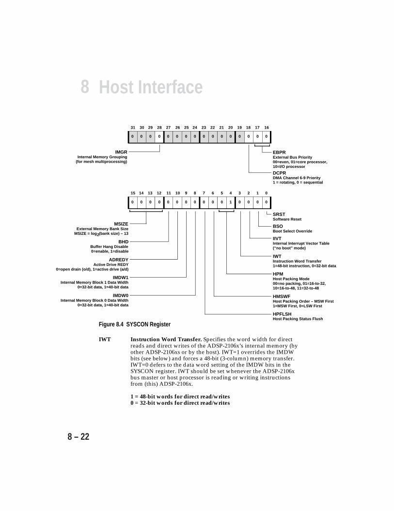
8 Host Interface
8 – 22
11 10 9 8 7 6 5 4 3 2 1 0
000010000000
15 14 13 12
0000
26 25 24 23 22 21 20 19 18 17
000000000000
31 30 29 28 27
0000
16
SRSTSoftware Reset
BSOBoot Select Override
IIVTInternal Interrupt Vector Table(“no boot” mode)
IWTInstruction Word Transfer1=48-bit instruction, 0=32-bit data
HPMHost Packing Mode00=no packing, 01=16-to-32,10=16-to-48, 11=32-to-48
HMSWFHost Packing Order – MSW First1=MSW First, 0=LSW First
MSIZEExternal Memory Bank Size
MSIZE = log2(bank size) – 13
HPFLSHHost Packing Status Flush
IMDW1Internal Memory Block 1 Data Width
0=32-bit data, 1=40-bit data
IMDW0Internal Memory Block 0 Data Width
0=32-bit data, 1=40-bit data
EBPRExternal Bus Priority00=even, 01=core processor,10=I/O processor
DCPRDMA Channel 6-9 Priority1 = rotating, 0 = sequential
IMGRInternal Memory Grouping
(for mesh multiprocessing)
BHDBuffer Hang Disable0=enable, 1=disable
ADREDYActive Drive REDY
0=open drain (o/d), 1=active drive (a/d)
Figure 8.4 SYSCON Register
IWT Instruction Word Transfer. Specifies the word width for directreads and direct writes of the ADSP-2106x’s internal memory (byother ADSP-2106xs or by the host). IWT=1 overrides the IMDWbits (see below) and forces a 48-bit (3-column) memory transfer.IWT=0 defers to the data word setting of the IMDW bits in theSYSCON register. IWT should be set whenever the ADSP-2106xbus master or host processor is reading or writing instructionsfrom (this) ADSP-2106x.
1 = 48-bit words for direct read/writes0 = 32-bit words for direct read/writes

8Host Interface
8 – 23
HPM Host Packing Mode. Specifies the internal word width andexternal host bus width for host processor accesses of theADSP-2106x’s internal memory or IOP registers. If the hostaccess is a read or write of any IOP register other than theexternal port FIFO buffers (EPB0-EPB3) or link port buffers(LBUF0-LBUF5), the word width will always be 32 bits no matterwhat the host bus width is. If the host access is a read or write ofthe link port buffers, the word width is determined only by HPM,and not by the LEXT bit in LCTL.
00 = No packing. Maximum bus width is 32 bits forasynchronous transfers. The lower 16 bits of the 48-bit data buswill be written and read as zeros, even when reading 48-bitwords. For synchronous transfers, the host bus should be 32 bitswide for data transfers or 48 bits wide for instruction wordtransfers. (Note: To read and write 48-bit words from internalmemory, the IWT bit must be set to 1 or the IMDW bit for theblock of memory being accessed must be set to 1.)
01 = 16-bit host bus, 32-bit words. The host bus will be 16 bitswide; any memory access will be 32-bit words. (Note: If thememory access is to a block of ADSP-2106x internal memory forwhich the IMDW bit is set to 1, the access will read or write theupper 32 bits of the 48-bit word.)
10 = 16-bit host bus, 48-bit words. The host bus will be 16 bitswide; any memory access will be 48-bit words.
11 = 32-bit host bus, 48-bit words. The host bus will be 32 bitswide; any memory access will be 48-bit words.
HMSWF Host Packing Order. Specifies the order in which host-accessedwords are packed, for 16-to-32 bit packing and 16-to-48 bitpacking. HMSWF is ignored for 32-to-48 bit packing. WhenHMSWF=1, packing is done MSW first (most significant 16-bitword first). When HMSWF=0, packing is is done LSW first.
1=MSW first0=LSW first
HPFLSH Host Packing Status Flush. Resets the host packing status. Hostaccesses must not occur while the HPFLSH bit is being writtenby the ADSP-2106x processor core. There is a two cycle latencybefore the reset takes effect, after which the host may resumenormal operations. (Note: HPFLSH is always read as a zero.)
1=Flush packing status
Default →at Reset
8 Host Interface
8 – 24
IMDWx Internal Memory Block Data Width. Selects the data wordwidth for each block of internal memory. For 32-bit data words,set IMDWx to 0. For 40-bit data (transferred within 48-bitwords), set IMDWx to 1. IMDW0 (bit 8 of SYSCON) selects thedata word width for memory block 0 and IMDW1 (bit 9) selectsthe data word width for memory block 1. (Note: 48-bitinstructions can be stored in a memory block regardless of thesetting of the IMDW bit. See “Configuring Memory For 32-Bit or40-Bit Data” in the Memory chapter of this manual for moreinformation.)
0=32-bit data1=40-bit data
In addition to the HPM bits, the packing mode is also affected by thesetting of the PMODE bits in the DMACx control register of eachexternal port buffer (DMAC6, DMAC7, DMAC8, and DMAC9, whichcorrespond to the EPB0, EPB1, EPB2, and EPB3 buffers):
PMODE Packing Mode00 No packing/unpacking01 16-bit external bus to/from 32-bit internal packing10 16-bit external bus to/from 48-bit internal packing11 32-bit external bus to/from 48-bit internal packing
HPM and PMODE must select the same external bus width for host datatransfers to and from the ADSP-2106x!!
For example, if HPM=11 for a 32-bit host bus, then PMODE must alsobe set to 11. If HPM equals 01 or 10 for a 16-bit bus, then PMODE canbe either 01 or 10.
If any of the three packing modes are used for non-DMA, single-wordtransfers to or from an EPBx buffer, the TRAN bit must also beappropriately set in the DMACx control register. Set TRAN=1 for hostreads from the EPBx buffer, or set TRAN=0 for host writes to the EPBxbuffer.
To change the host packing mode, the following sequence must occur:
1. Write to the SYSCON register, changing the value of HPM.2. Read SYSCON to ensure that the write was completed.3. Repeat the write to SYSCON (to flush the read, since it may have
occurred in the old packing mode).4. Wait 4 cycles.
8Host Interface
8 – 25
During packed transfers with a slow host, the host may relinquish thebus before the current word has been fully packed—the bus may bereleased after the first part of the word is written and then, some timelater, HBR reasserted and the second part of the word written. Thiscould allow, for example, another ADSP-2106x to write to this onewithout affecting the host packing operation.
8.5.2 Data Bus Lines Used For Different Packing ModesTable 8.4 shows which data bus lines are used for different host buswidths and packing modes. If the host bus width is 32 bits and nopacking is selected for an asynchronous access, the ADSP-2106x willignore the lower 16 bits of the 48-bit external data bus when inputtingdata—note that this only true for asynchronous accesses, not for synchronousaccesses. When outputting data onto a 32-bit host bus with 48-to-32 bitunpacking, the ADSP-2106x drives the lower 16 bits as zeroes; this istrue for both asynchronous and synchronous accesses. Whenoutputting data with no packing, the ADSP-2106x drives the lower16 bits with whatever data is in the corresponding memory bits; thisapplies for both asynchronous and synchronous accesses.
If the host bus width is 16 bits and 16-to-32 or 16-to-48 bit packing isselected, the ADSP-2106x will ignore the upper and lower 16 bits of the48-bit external data bus when inputting data (for both asynchronousand synchronous accesses). When outputting data, these bits will bedriven as zeroes.
Host HPMPacking Bits InMode* SYSCON EffectNo packing 00 Data In: ADSP-2106x ignores lower 16 bits of external bus (DATA15-0)
for a 32-bit host (asynchronous accesses only).Data Out: ADSP-2106x outputs whatever is in memory onto theexternal bus (DATA47-0).
16-to-32 01 Data In: ADSP-2106x ignores upper and lower 16 bits of external bus.Data Out: ADSP-2106x outputs zeroes on upper and lower 16 bits ofexternal bus.
16-to-48 10 Same as 16-to-32 packing.
32-to-48 11 Data In: ADSP-2106x ignores lower 16 bits of external bus (DATA15-0).Data Out: ADSP-2106x outputs zeroes on lower 16 bits of external bus.
Table 8.4 Data Bus Lines Used For Different Host Packing Modes
* 16-to-32 packing: 16-bit host bus, 32-bit memory words on ADSP-2106x.16-to-48 packing: 16-bit host bus, 48-bit memory words on ADSP-2106x.32-to-48 packing: 32-bit host bus, 48-bit memory words on ADSP-2106x.
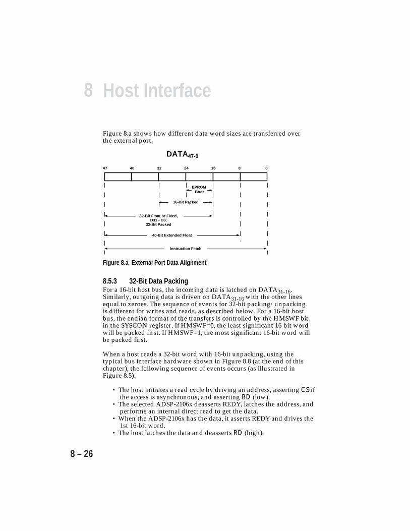
8 Host Interface
8 – 26
Figure 8.a shows how different data word sizes are transferred overthe external port.
081624324047
DATA47-0
EPROMBoot
16-Bit Packed
32-Bit Float or Fixed,D31 - D0,
32-Bit Packed
40-Bit Extended Float
Instruction Fetch
Figure 8.a External Port Data Alignment
8.5.3 32-Bit Data PackingFor a 16-bit host bus, the incoming data is latched on DATA31-16.Similarly, outgoing data is driven on DATA31-16 with the other linesequal to zeroes. The sequence of events for 32-bit packing/unpackingis different for writes and reads, as described below. For a 16-bit hostbus, the endian format of the transfers is controlled by the HMSWF bitin the SYSCON register. If HMSWF=0, the least significant 16-bit wordwill be packed first. If HMSWF=1, the most significant 16-bit word willbe packed first.
When a host reads a 32-bit word with 16-bit unpacking, using thetypical bus interface hardware shown in Figure 8.8 (at the end of thischapter), the following sequence of events occurs (as illustrated inFigure 8.5):
• The host initiates a read cycle by driving an address, asserting CS ifthe access is asynchronous, and asserting RD (low).
• The selected ADSP-2106x deasserts REDY, latches the address, andperforms an internal direct read to get the data.
• When the ADSP-2106x has the data, it asserts REDY and drives the1st 16-bit word.
• The host latches the data and deasserts RD (high).
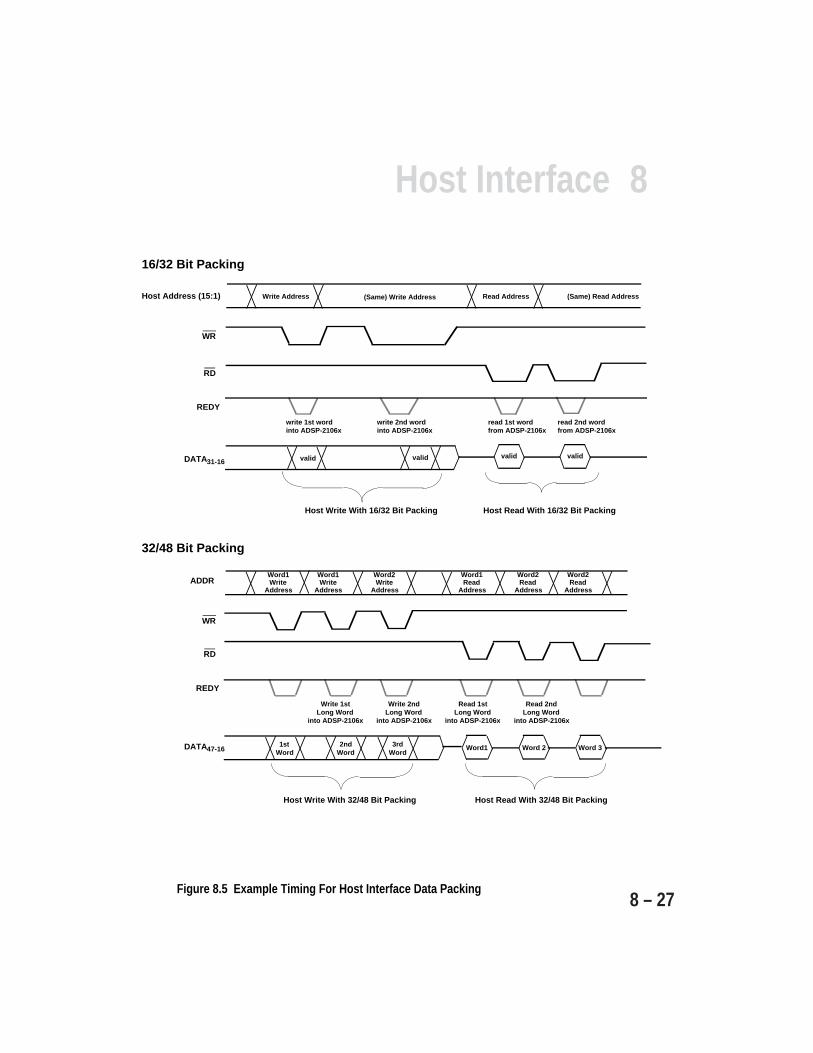
8Host Interface
8 – 27Figure 8.5 Example Timing For Host Interface Data Packing
Write Address (Same) Write Address Read Address (Same) Read Address
REDY
write 1st wordinto ADSP-2106x
write 2nd wordinto ADSP-2106x
read 1st wordfrom ADSP-2106x
read 2nd wordfrom ADSP-2106x
valid valid valid valid
16/32 Bit Packing
Host Address (15:1)
DATA31-16
Host Write With 16/32 Bit Packing Host Read With 16/32 Bit Packing
Word1Write
Address
1st Word
Word1
REDY
32/48 Bit Packing
ADDR
DATA47-16
Word1Write
Address
Word2Write
Address
Word1Read
Address
Word2Read
Address
Word2Read
Address
Write 1st Long Word
into ADSP-2106x
Write 2nd Long Word
into ADSP-2106x
Read 1st Long Word
into ADSP-2106x
Read 2nd Long Word
into ADSP-2106x
2nd Word
3rd Word
Word 2 Word 3
Host Write With 32/48 Bit Packing Host Read With 32/48 Bit Packing
WR
RD
WR
RD

8 Host Interface
8 – 28
• The host initiates another read access, driving the address of the datato be accessed and then asserting RD.
• The ADSP-2106x transmits the 2nd 16-bit word.
When a host writes a 32-bit word with 16-bit packing, again using thetypical bus interface hardware shown in Figure 8.8, the followingsequence of events occurs (also illustrated in Figure 8.5):
• The host initiates a write cycle by driving the write address, assertingCS if the access is asynchronous, and asserting WR (low).
• The ADSP-2106x asserts REDY when it is ready to accept data.• The host drives the address and the 1st 16-bit word, and deassertsWR (high).
• The ADSP-2106x latches the 1st 16-bit word.• The host again drives the address and initiates another write cycle
for the 2nd 16-bit word, by asserting WR.• When the ADSP-2106x has accepted the 2nd word it performs an
internal direct write to its memory (or memory-mapped IOPregister). If the ADSP-2106x’s internal write has not completed bythe time another host access occurs, that access will be held off withREDY.
If the ADSP-2106x is waiting for another 16-bit word from the host tocomplete the packed word, the HPS bits in the SYSTAT register will benon-zero. (See “SYSTAT Register Status Bits.”) Because there is onlyone packing buffer for the host interface, the host must fully completeeach packed read or write before another is begun.
8.5.4 48-Bit Instruction PackingThe host can also download and upload 48-bit instructions over its16- or 32-bit bus. The packing sequence for downloading ADSP-2106xinstructions from a 32-bit host bus (HPM=11) takes 3 cycles for every2 words, as illustrated below. 32-bit data is transferred on data buslines 47-16 (DATA47-16). If an odd number of instruction words aretransferred, the packing buffer must be flushed by a dummy access toremove the unused word.

8Host Interface
8 – 29
32-Bit to 48-Bit Word Packing (Host Bus ↔ ADSP-2106x):Data Bus Lines 47-32 Data Bus Lines 31-16
1st transfer Word1, bits 47-32 Word1, bits 31-162nd transfer Word2, bits 15-0 Word1, bits 15-03rd transfer Word2, bits 47-32 Word2, bits 31-16
The HMSWF bit of SYSCON is ignored for 32-to-48-bit packing.
The packing sequence for downloading or uploading ADSP-2106xinstructions over a 16-bit host bus takes 3 cycles for every word, asshown below. The HMSWF bit in SYSCON determines whether the mostsignificant 16-bit word or least significant 16-bit word is packed first.
16-Bit to 48-Bit Word Packing w/HMSWF=1 (Host Bus ↔ ADSP-2106x):Data Bus Pins 31-16
1st transfer Word1 bits 47-322nd transfer Word1 bits 31-163rd transfer Word1 bits 15-0
40-bit extended precision data may be transferred using the 48-bitpacking mode. Refer to the Memory chapter of this manual for adiscussion of memory allocation for the different word widths.
8.6 SYSTAT REGISTER STATUS BITSThe SYSTAT register provides status information, primarily formultiprocessor systems. Table 8.5 shows the status bits in this register.
Bit(s)Name DefinitionHSTM Host MastershipBSYN Bus SynchronizationCRBM Current Bus Master (ID2-0 of ADSP-2106x bus master)IDC ID Code (ID2-0 of this ADSP-2106x)DWPD Direct Write PendingVIPD Vector Interrupt PendingHPS Host Packing Status
Table 8.5 SYSTAT Status Bits
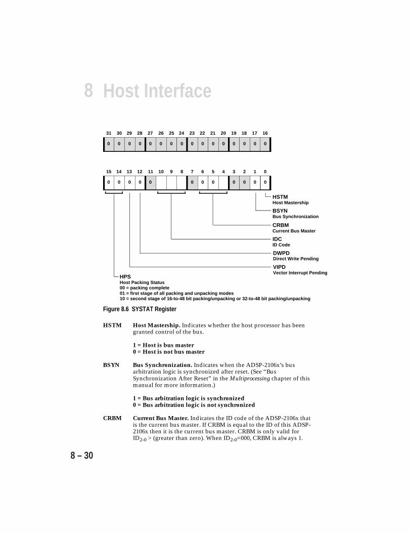
8 Host Interface
8 – 30
11 10 9 8 7 6 5 4 3 2 1 0
00000000
15 14 13 12
0000
26 25 24 23 22 21 20 19 18 17
000000000000
31 30 29 28 27
0000
16
HSTMHost Mastership
CRBMCurrent Bus Master
DWPDDirect Write Pending
HPSHost Packing Status00 = packing complete01 = first stage of all packing and unpacking modes10 = second stage of 16-to-48 bit packing/unpacking or 32-to-48 bit packing/unpacking
BSYNBus Synchronization
IDCID Code
VIPDVector Interrupt Pending
Figure 8.6 SYSTAT Register
HSTM Host Mastership. Indicates whether the host processor has beengranted control of the bus.
1 = Host is bus master0 = Host is not bus master
BSYN Bus Synchronization. Indicates when the ADSP-2106x’s busarbitration logic is synchronized after reset. (See “BusSynchronization After Reset” in the Multiprocessing chapter of thismanual for more information.)
1 = Bus arbitration logic is synchronized0 = Bus arbitration logic is not synchronized
CRBM Current Bus Master. Indicates the ID code of the ADSP-2106x thatis the current bus master. If CRBM is equal to the ID of this ADSP-2106x then it is the current bus master. CRBM is only valid forID2-0 > (greater than zero). When ID2-0=000, CRBM is always 1.

8Host Interface
8 – 31
IDC ID Code. Indicates the ID2-0 inputs of this ADSP-2106x.
DWPD Direct Write Pending. Indicates when a direct write to theADSP-2106x’s internal memory is pending. The DWPD bit is clearedwhen the direct write has been completed. (Direct writes may bedelayed for several cycles if DMA chaining is underway or if higherpriority DMA requests occur. Maximum delay is 12 cycles.)
1 = Direct write pending0 = No direct write pending
VIPD Vector Interrupt Pending. Indicates that a pending vector interrupthas not yet been serviced. The VIPD bit is set when the VIRPTregister is written to and is cleared upon return from the interruptservice routine. The host processor (or other ADSP-2106x) that issuedthe vector interrupt should monitor this bit to determine when theservice routine has been completed (and when a new vectorinterrupt may be issued).
1 = Vector interrupt pending0 = No vector interrupt pending
HPS Host Packing Status. Indicates when host word packing iscompleted or, if not, what stage of the process is taking place.(See “Host Packing” for more information.)
00 = Packing complete01 = 1st stage of all packing and unpacking modes.10 = 2nd stage of 16-to-48 bit packing/unpacking or 32-to-48 bit
packing/unpacking
8.7 INTERPROCESSOR MESSAGES & VECTOR INTERRUPTSOnce it has requested and been granted control of the ADSP-2106x, thehost processor communicates with the ADSP-2106x by writing messagesto the memory-mapped IOP registers. Asynchronous writes are theeasiest way for the host to do this. In a multiprocessor system, the hostcan access the internal memory and IOP registers of every ADSP-2106x.
The MSGR0-MSGR7 registers are general-purpose registers that can beused for convenient message passing between the host and ADSP-2106x.They are also useful for semaphores and resource sharing betweenmultiple ADSP-2106xs. The MSGRx and VIRPT registers can be used formessage passing in the following ways:
• Message Passing. The host can use any of the 8 message registers,MSGR0–MSGR7, to communicate with the ADSP-2106x.
8 Host Interface
8 – 32
• Vector Interrupts. The host can issue a vector interrupt to theADSP-2106x by writing the address of an interrupt service routine tothe VIRPT register. This causes an immediate high-priority interrupt onthe ADSP-2106x which, when serviced, will cause the ADSP-2106x tobranch to the specified service routine.
The MSGRx and VIRPT registers also support shared-busmultiprocessing via the external port. Since these registers may beshared resources within a single ADSP-2106x, conflicts may occur—your system software must prevent this. For further discussion of IOPregister access conflicts, refer to the Control/Status Registers appendix ofthis manual.
8.7.1 Message Passing (MSGRx)Three possible software protocols by which a host can communicatewith the ADSP-2106x through the MSGRx message registers are:1) vector-interrupt-driven, 2) register handshake, and 3) register write-back.
For the vector-interrupt-driven method, the host fills predeterminedMSGRx registers with data and triggers a vector interrupt by writingthe address of the service routine to VIRPT. The service routine shouldread the data from the MSGRx registers and then write “0” into VIRPTto tell the host it is done. The service routine could also use one of theADSP-2106x’s FLAG3-0 pins to tell the host it has finished.
For the register handshake method, four of the MSGRx registers shouldbe designated as follows: a receive register (R), a receive handshakeregister (RH), a transmit register (T), and a transmit handshake register(TH). To pass data to the ADSP-2106x, the host would write data into Tand then write a “1” into TH. When the ADSP-2106x sees a “1” in TH,it reads the data from T and then writes back a “0” into TH. When thehost sees a “0” in TH, it knows that the transfer is complete. A similarsequence of events occurs when the ADSP-2106x passes data to thehost through R and RH.
The register write-back method is similar to register handshaking, butuses only the T and R data registers. The host writes data to T. Whenthe ADSP-2106x sees a non-zero value in T, it retrieves it and writesback a “0” to T. A similar sequence occurs when the host is receivingdata. This simpler method works well as long as the data to be passeddoes not include “0.”
8Host Interface
8 – 33
8.7.2 Host Vector Interrupts (VIRPT)Vector interrupts are used for interprocessor commands between thehost and an ADSP-2106x or between two ADSP-2106xs. When theexternal processor writes an address to the ADSP-2106x’s VIRPTregister a vector interrupt is caused.
When the vector interrupt is serviced, the ADSP-2106x automaticallypushes the status stack and begins executing the service routinelocated at the address specified in VIRPT. The lower 24 bits of VIRPTcontain the address; the upper 8 bits may be optionally used as data tobe read by the interrupt service routine. At reset, VIRPT is initialized toits standard address in the ADSP-2106x’s interrupt vector table.
The minimum latency for vector interrupts is six cycles, five of whichare NOPs. When the RTI (return from interrupt) instruction is reachedin the service routine, the ADSP-2106x automatically pops the statusstack.
The VIPD bit in the SYSTAT register reflects the status of the VIRPTregister. If VIRPT is written while a previous vector interrupt ispending, the new vector address replaces the pending one. If VIRPT iswritten while a previous vector interrupt is being serviced, the newvector address is ignored and no new interrupt is generated. If theADSP-2106x writes to its own VIRPT register, no interrupt isgenerated.
To use the ADSP-2106x’s vector interrupt feature, the host couldperform the following sequence of actions:
1. Poll the VIRPT register until it reads a certain token value (i.e. zero).2. Write the vector interrupt service routine address to VIRPT.3. When the service routine is finished, the ADSP-2106x should write
the token back into VIRPT to indicate that it is finished and thatanother vector interrupt can be initiated.
The DWPD (Direct Write Pending) bit of the SYSTAT register indicateswhen a direct write to internal memory is pending. Direct writes andIOP register accesses may be completed in different sequences. If, forexample, the host performs a direct memory write to an ADSP-2106xand then writes to an IOP register on the ADSP-2106x, the IOP register
8 Host Interface
8 – 34
write may complete before the direct write. Because of this, directwrites performed just before vector interrupt writes (to VIRPT) may bedelayed until after the branch to the interrupt vector:
1. The host processor performs a direct write to the internal memory ofan ADSP-2106x.
2. The host processor writes to the VIRPT register of the ADSP-2106xto initiate a vector interrupt. This causes the direct write to bedelayed.
4. The ADSP-2106x jumps to the vector interrupt service routine.5. The direct write is completed after the interrupt service routine is
underway.
To prevent this from happening, the host should check that all directwrites have completed before writing to the ADSP-2106x’s VIRPTregister. This can be done by polling the ADSP-2106x’s DWPD bit (inSYSTAT) after performing a direct write, waiting for it to becomecleared, and then proceeding with the write to VIRPT.
8.8 SYSTEM BUS INTERFACINGAn ADSP-2106x subsystem, consisting of several ADSP-2106xs withlocal memory, may be viewed as one of several processing elementsconnected together by a system bus. Examples of such systems are theEISA bus, PCI bus, or even several ADSP-2106x subarrays. Theprocessing elements in such a system arbitrate for the system bus viaan arbitration unit. Each device on the bus that wishes to become a busmaster must be able to drive a bus request signal and respond to a busgrant signal. The arbitration unit determines which request it willgrant in any given cycle.
8.8.1 Access To The ADSP-2106x Bus—Slave ADSP-2106xFigure 8.7 shows an example of a basic interface to a system bus whichisolates the local ADSP-2106x bus from the system bus. When thesystem is not accessing the ADSP-2106xs, the local bus supportstransfers between other local ADSP-2106xs and/or local externalmemory or devices.
When the system wishes to access an ADSP-2106x, it executes a read orwrite to the address range of the ADSP-2106x subsystem. The externaladdress comparator detects a local access and asserts HBR and one ofthe appropriate CS lines. The system bus is held off by REDY until theADSP-2106x is ready to accept the data. The HBG signal enables thesystem bus buffers. The buffers’ direction for data is controlled by the
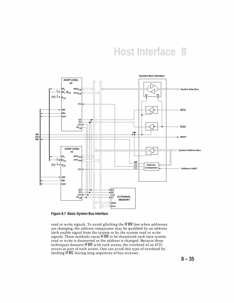
8Host Interface
8 – 35
ADSP-2106x#1
ADDADDRR31-031-0DATADATA47-047-0
IDID2-02-0
ADSP-2106x#2
ADDRADDR31-031-0
DATADATA47-047-0
IDID2-02-0
WRWRRDRD
ACKMSMS3-03-0
HBRHBR
HBGHBG
BRBR2-62-6
BRBR11
001
010
, BRBR3-63-6BRBR11
5
3
3
BRBR225
HBRHBR
HBGHBG
WRWRRDRD
ACKMSMS3-03-0
ADDRADDR
DATADATA
EXTERNALMEMORY
CSCSACKOEOEWEWE
System Data Bus
REDYREDY
REDYREDY
Write
Read
System Address Bus
AddressComparator "Address Valid"CS1CS1
HBGHBG
HBRHBR
CS2CS2
CS2CS2CS1CS1
REDYHBGHBGREDYREDYHBRHBR
System Bus Interface
OEOE T/T/RR
Figure 8.7 Basic System Bus Interface
read or write signals. To avoid glitching the HBR line when addressesare changing, the address comparator may be qualified by an addresslatch enable signal from the system or by the system read or writesignals. These methods cause HBR to be deasserted each time systemread or write is deasserted or the address is changed. Because thesetechniques deassert HBR with each access, the overhead of an HTCoccurs as part of each access. One can avoid this type of overhead bylatching HBG during long sequences of bus accesses.
8 Host Interface
8 – 36
8.8.2 Access To The System Bus—Master ADSP-2106xFigure 8.8 shows a more complex, bidirectional system interface inwhich the ADSP-2106x subsystem can access the system bus bybecoming a bus master. Before it begins the access, the ADSP-2106xmust first request permission to become the bus master by generatingthe System Bus Request signal (SBR). The system bus arbitration unitdetermines when to respond with the System Bus Grant signal (SBG).In this system, each system bus master generates and responds to itsown unique pair of signals.
The method an ADSP-2106x uses to arbitrate for the system busdepends on whether the access is from the ADSP-2106x processor coreor from its DMA controller. These two methods, which are quitedifferent, are described below under “Core Processor Access ToSystem Bus” and “ADSP-2106x DMA Access To System Bus.”
8.8.2.1 Core Processor Access To System BusThe ADSP-2106x core may arbitrate for the system bus by setting a flagand waiting for SBG via another flag. This has the benefit of not tyingup the local bus while waiting. If SBG is tied to an interrupt pin, thenuseful work can continue while waiting.
Another method is to attempt the access assuming that the system busis available, and then either wait or abort the access if it is notavailable. The ADSP-2106x begins the access to the system bus byasserting one of the memory select lines, MS3. This also asserts SBR. Ifthe system bus is not available, i.e. SBG is deasserted, the ADSP-2106xshould be held off with ACK. This approach is simple but ties up theADSP-2106x and the local bus whenever the system bus is accessedwhile it is busy. To overcome this, the Type 10 instruction
IF condition JUMP(addr), ELSE compute, DM(addr)=dreg;
can be used. This instruction aborts the bus access if the condition(SBG) is not true, and causes a branch to a “try again later” routine.This method works well if SBG is asserted most of the time. If theType 10 instruction is not used, a deadlock condition can result if anaccess is attempted before the bus is granted, as described in the nextsection.

8Host Interface
8 – 37
Figure 8.8 Bidirectional System Bus Interface
Note: The memory controller for shared external memory must generate wait statesand REDY for host accesses to the memory.
ADSP-2106x#1
ADDADDRR31-031-0DATADATA47-047-0
IDID2-02-0
ADSP-2106x#2
ADDRADDR31-031-0
DATADATA47-047-0
IDID2-02-0
WRWRRDRD
ACKMSMS3-03-0
HBRHBR
HBGHBG
BRBR2-62-6
BRBR11
001
010
, BRBR3-63-6BRBR11
5
3
3
BRBR225
HBRHBRHBGHBG
WRWRRDRD
ACKMSMS3-03-0
ADDRADDR
DATADATA
EXTERNALMEMORY
CSCSACKOEOEWEWE
System Data Bus
REDYREDY
REDYREDY
Host Write
Host Read
System Address Bus
FLAG0FLAG0
FLAG0FLAG0
System Bus Grant
AddressComparator "Address Valid"CS1CS1
SBTSSBTS
HBGHBG
HBRHBR
CS2CS2
SBTSSBTS
CS2CS2CS1CS1
REDYHBGHBGREDYREDYHBRHBR
ACKMSMS3-03-0
System Bus Request
System Bus Interface
WRWRRDRD
HBGHBG
8 Host Interface
8 – 38
8.8.2.2 Deadlock ResolutionIn the rare case where both the ADSP-2106x subsystem and the systemare trying to access each other’s bus in the same cycle, a deadlock mayoccur in which neither access can complete; ACK stays deasserted.
Normally the master ADSP-2106x will respond to an HBR request byasserting HBG after the completion of the current access. If theADSP-2106x is accessing the system bus at the same time, however,HBG will not be asserted because this current access cannotcomplete—this results in a deadlock in which neither access cancomplete. The deadlock may be broken by asserting the SBTS input forone or more cycles once the deadlock is detected (i.e. when the systembus to local bus buffer is enabled from both sides). SBTS is the SuspendBus Tristate pin of the ADSP-2106x.
The combination of SBTS and HBR puts the master ADSP-2106x intoslave mode, just like a normal HBR assertion, and suspends theADSP-2106x core’s external access. This allows the system access to thelocal bus to proceed, once the ADSP-2106x asserts HBG. Thecombination of HBR and SBTS should only be applied when there is adeadlock caused by an ADSP-2106x access to the system bus. It shouldnot be used when there is a local bus transfer because the WR signalwill be asserted twice, once before the SBTS is asserted and once afterthe access resumes. For SHARC-to-SHARC transfers on the local bus,this will violate the slave timing requirements.
The following sequence of actions allows the host processor to suspendan ongoing ADSP-2106x access and gain access to its internalresources, provided that: 1) the access originates from theADSP-2106x’s core, not the DMA controller, 2) a DRAM PAGE miss isnot detected for that memory access, and 3) bus lock is not enabled.
1. After HBR is asserted, the host asserts SBTS for one or more cycles.If SBTS is asserted one or more cycles after HBR is recognized, HBGis guaranteed to be asserted in the next cycle. SBTS should bedeasserted before HBR is deasserted.
2. The host drives both RD and WR strobes to their correct value(within the setup time specified in the data sheet) after HBG isasserted. The host may then perform as many accesses as desired.
3. The host has full control of the bus and may access any of theADSP-2106xs or peripherals on the bus.

8Host Interface
8 – 39
4. The host deasserts HBR. HBG will be deasserted when the internalread buffer is empty.
5. One cycle after the ADSP-2106x deasserts HBG, the ADSP-2106xrestarts its suspended access.
8.8.2.3 ADSP-2106x DMA Access To System BusThe use of the SBTS and HBR inputs to resolve a system bus deadlock,as described above, cannot be used for DMA transfers because once aDMA word transfer has begun in the ADSP-2106x, it must becompleted (i.e. it must receive the ACK signal). If SBTS and HBR areasserted during a DMA access, the HBG pin will not be asserted untilthe access cycle has completed. If the single DMA access is not allowedto complete, a deadlock condition may result.
To prevent system bus deadlock when using DMA, you must ensurethat SBG has been asserted before the DMA sequence begins. If ahigher priority access is needed, the DMA sequence may be held off(by asserting HBR) at any time after a word has been transferred. Youmust make sure that SBG is asserted before HBR is deasserted toprevent the possibility of another deadlock occurring. When the DMAsequence is complete, the DMA interrupt service routine should clearthe external SBR flag.
Because the system bus is likely to be considerably slower than theADSP-2106x local bus, performance on the local bus may beconsiderably improved by using handshake mode DMA. In this case,the SBG signal is tied to the DMA request line, DMARx. Thus the localbus and system bus access will only be initiated when the system busis available.
The use of a FIFO in the system interface unit, to allow DMA data fromthe local bus to be posted, may also increase performance on the localbus when using a slow system bus.
8 Host Interface
8 – 40
8.8.3 Multiprocessing With Local MemoryFigure 8.9 shows how several ADSP-2106x subsystems may beconnected together on a system bus for high throughput. The gatearray implements bus arbitration when the system bus is accessed. Thebuffers isolate the ADSP-2106x local buses from the system bus.
This example system works in the following way:
• An ADSP-2106x requests the system bus with SBR when it assertsthe MS3 line (for example). The gate array arbitrates between theSBR lines and then enables the highest priority group by assertingSBG, which is tied to ACK.
• The master ADSP-2106x may connect to system memory or to otherADSP-2106x groups. When the bus buffer is enabled, the read orwrite strobe enables should be asserted with a delay to allow theaddress to stabilize.
• To access an ADSP-2106x slave in another group, the masterADSP-2106x addresses that group’s multiprocessor memory space.The gate array detects group multiprocessor memory space fromthree high-order address bits and asserts the HBR line for theselected group. When HBG is asserted, the gate array enables theslave’s bus buffer. The high-order group address bits are cleared bythe buffer to allow the group to decode the E, M, and S addressfields as local multiprocessor memory space. The access will besynchronous because the CS line is not asserted. The single waitstate option for the bus should be enabled.
• If two groups access each other in the same cycle, a deadlock mayoccur. The SBTS pin may be used to clear the deadlock.
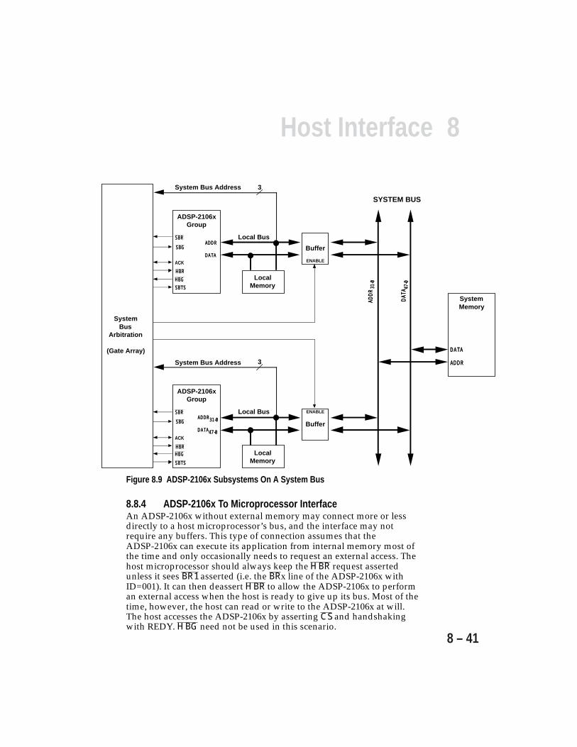
8Host Interface
8 – 41
ADSP-2106xGroup
ACK
HBRHBRHBGHBG
ADDRADDR31-031-0
DATADATA47-047-0
LocalMemorySBTSSBTS
Buffer
ENABLELocal Bus
System Bus Address 3
SBGSBG
SBRSBR
ADSP-2106xGroup
ACK
HBRHBRHBGHBG
ADDRADDR
DATADATA
LocalMemorySBTSSBTS
Local Bus
System Bus Address 3
SBGSBG
SBRSBR
Buffer
ENABLE
SystemBus
Arbitration
(Gate Array)
SYSTEM BUS
ADDR
ADDR
31-0
31-0
DATA
DATA
47-0
47-0
SystemMemory
ADDRADDR
DATADATA
Figure 8.9 ADSP-2106x Subsystems On A System Bus
8.8.4 ADSP-2106x To Microprocessor InterfaceAn ADSP-2106x without external memory may connect more or lessdirectly to a host microprocessor’s bus, and the interface may notrequire any buffers. This type of connection assumes that theADSP-2106x can execute its application from internal memory most ofthe time and only occasionally needs to request an external access. Thehost microprocessor should always keep the HBR request assertedunless it sees BR1 asserted (i.e. the BRx line of the ADSP-2106x withID=001). It can then deassert HBR to allow the ADSP-2106x to performan external access when the host is ready to give up its bus. Most of thetime, however, the host can read or write to the ADSP-2106x at will.The host accesses the ADSP-2106x by asserting CS and handshakingwith REDY. HBG need not be used in this scenario.

8 Host Interface
8 – 42
9
9 – 1
Link Ports
9.1 OVERVIEWThe ADSP-2106x SHARC provides additional I/O capability throughsix dedicated 4-bit link ports. Each link port consists of fourbidirectional data lines, a bidirectional clock line, and a bidirectionalacknowledge line. The link ports can be clocked twice per processorclock cycle, allowing each port to transfer up to 8 bits of data per cycle.Link port I/O allows a variety of interconnection schemes to I/Operipheral devices as well as coprocessing and multiprocessingschemes. Using link port I/O, it is also possible to configuremultidimensional, multiprocessor arrays.
Note that the ADSP-21061 processor does not have link ports; thediscussion in this chapter does not apply to the ADSP-21061.
Link port features and functions include:
• Link ports can operate independently and simultaneously.• Link port data is packed into 32-bit or 48-bit words, and can be directly
read by the ADSP-2106x core processor or DMA-transferred to on-chipmemory.
• Link port data can also be accessed by the external host processor, usingdirect reads and writes.
• Double-buffered transmit and receive data registers.• Clock/acknowledge handshaking controls link port transfers which are
programmable as either transmit or receive with each link portsupported by a separate DMA channel.
• Link ports provide high-speed, point-to-point data transfers to otherADSP-2106x processors. This allows a variety of interconnectionschemes between multiple ADSP-2106x processors and externaldevices, including 1-, 2- and 3-dimensional arrays.
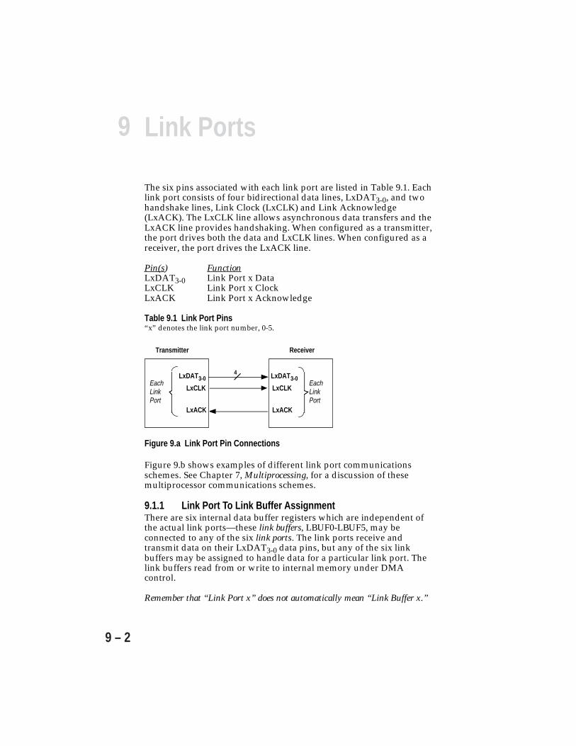
9 Link Ports
9 – 2
The six pins associated with each link port are listed in Table 9.1. Eachlink port consists of four bidirectional data lines, LxDAT3-0, and twohandshake lines, Link Clock (LxCLK) and Link Acknowledge(LxACK). The LxCLK line allows asynchronous data transfers and theLxACK line provides handshaking. When configured as a transmitter,the port drives both the data and LxCLK lines. When configured as areceiver, the port drives the LxACK line.
Pin(s) FunctionLxDAT3-0 Link Port x DataLxCLK Link Port x ClockLxACK Link Port x Acknowledge
Table 9.1 Link Port Pins“x” denotes the link port number, 0-5.
Figure 9.a Link Port Pin Connections
Figure 9.b shows examples of different link port communicationsschemes. See Chapter 7, Multiprocessing, for a discussion of thesemultiprocessor communications schemes.
9.1.1 Link Port To Link Buffer AssignmentThere are six internal data buffer registers which are independent ofthe actual link ports—these link buffers, LBUF0-LBUF5, may beconnected to any of the six link ports. The link ports receive andtransmit data on their LxDAT3-0 data pins, but any of the six linkbuffers may be assigned to handle data for a particular link port. Thelink buffers read from or write to internal memory under DMAcontrol.
Remember that “Link Port x” does not automatically mean “Link Buffer x.”
Transmitter
EachLinkPort
LxCLK
LxACK
LxDAT3-0
Receiver
EachLinkPort
LxCLK
LxACK
LxDAT3-04
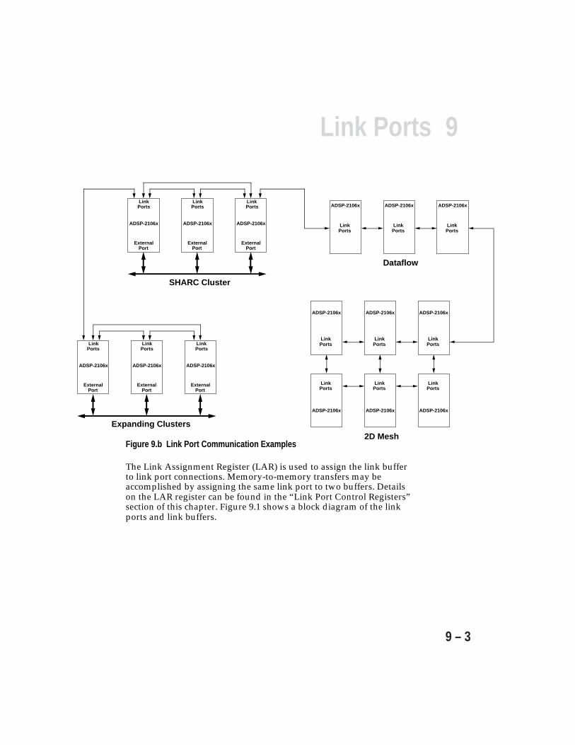
9Link Ports
9 – 3
ADSP-2106x ADSP-2106x ADSP-2106x
ADSP-2106x
LinkPorts
ADSP-2106x
LinkPorts
ADSP-2106x
LinkPorts
External Port
External Port
External Port
SHARC Cluster
ADSP-2106x
LinkPorts
ADSP-2106x
LinkPorts
ADSP-2106x
LinkPorts
External Port
External Port
External Port
Expanding Clusters
LinkPorts
LinkPorts
LinkPorts
Dataflow
ADSP-2106x ADSP-2106x ADSP-2106x
LinkPorts
LinkPorts
LinkPorts
ADSP-2106x ADSP-2106x ADSP-2106x
LinkPorts
LinkPorts
LinkPorts
2D MeshFigure 9.b Link Port Communication Examples
The Link Assignment Register (LAR) is used to assign the link bufferto link port connections. Memory-to-memory transfers may beaccomplished by assigning the same link port to two buffers. Detailson the LAR register can be found in the “Link Port Control Registers”section of this chapter. Figure 9.1 shows a block diagram of the linkports and link buffers.
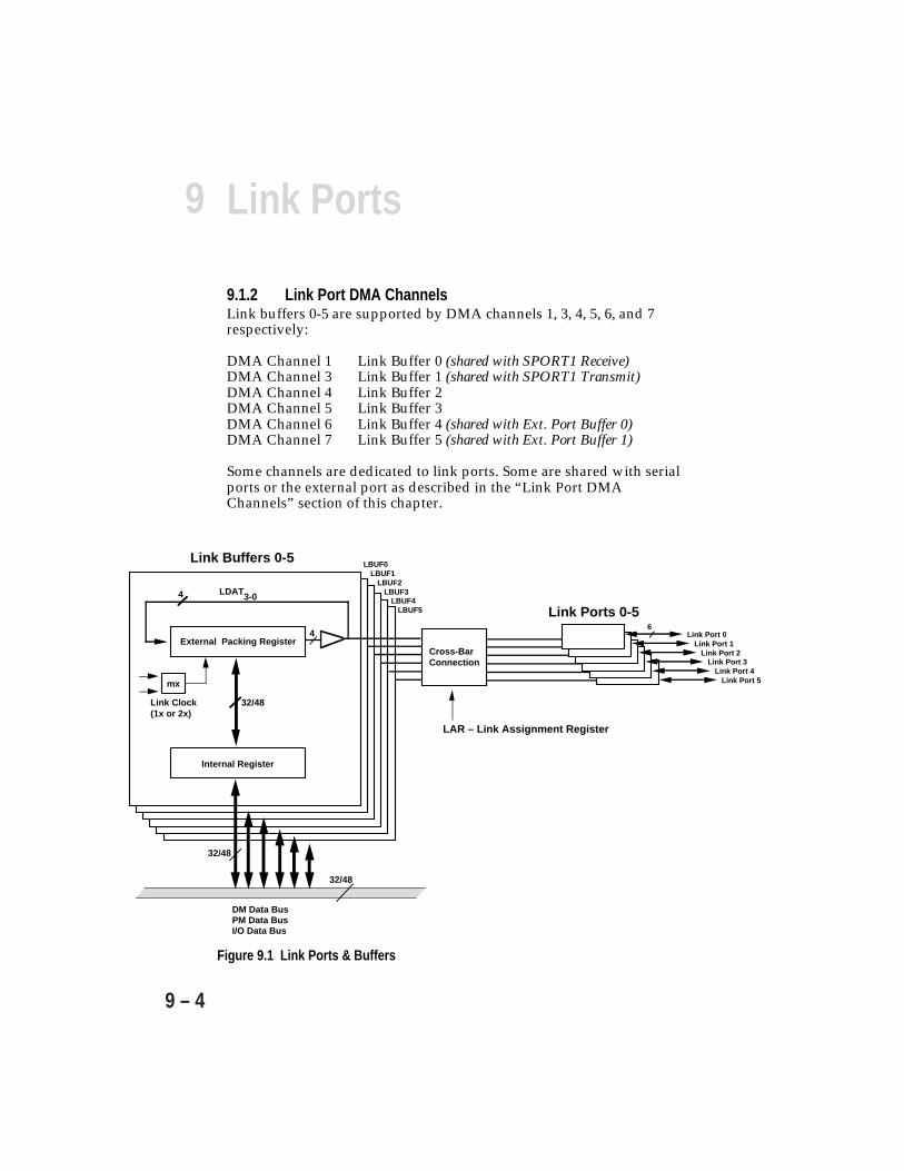
9 Link Ports
9 – 4
9.1.2 Link Port DMA ChannelsLink buffers 0-5 are supported by DMA channels 1, 3, 4, 5, 6, and 7respectively:
DMA Channel 1 Link Buffer 0 (shared with SPORT1 Receive)DMA Channel 3 Link Buffer 1 (shared with SPORT1 Transmit)DMA Channel 4 Link Buffer 2DMA Channel 5 Link Buffer 3DMA Channel 6 Link Buffer 4 (shared with Ext. Port Buffer 0)DMA Channel 7 Link Buffer 5 (shared with Ext. Port Buffer 1)
Some channels are dedicated to link ports. Some are shared with serialports or the external port as described in the “Link Port DMAChannels” section of this chapter.
External Packing Register
4
4
Link Clock(1x or 2x)
mx
Cross-BarConnection
Link Buffers 0-5
LAR – Link Assignment Register
LDAT3-0
Internal Register
DM Data BusPM Data BusI/O Data Bus
32/48
32/48
6
LBUF0LBUF1
LBUF2LBUF3
LBUF4LBUF5
Link Port 0Link Port 1
Link Port 2Link Port 3
Link Port 4Link Port 5
32/48
Link Ports 0-5
Figure 9.1 Link Ports & Buffers
9Link Ports
9 – 5
9.1.3 Link Port InterruptsThree types of interrupts are dedicated to the link ports:
• If DMA is enabled, a maskable interrupt is generated when the DMAblock transfer has completed.
• If DMA is disabled, then the link buffer may be read or written by thecore processor as a memory-mapped location (part of the IOP registerspace). A maskable interrupt is generated while DMA is disabled andthe receive buffer is not empty, or if the transmit buffer is not full.
• When an external source accesses an unassigned link port (or accessesan assigned link port that has its link buffer disabled), this access causesa maskable LSRQ interrupt.
9.1.4 Link Port BootingThe link ports may be used to load internal memory at reset. Refer tothe section “Booting” in the System Design chapter of this manual fordetails of this operation.
9.2 LINK PORT CONTROL REGISTERSThere are three link port control registers: the Link Buffer ControlRegister (LCTL), the Link Common Control Register (LCOM), and theLink Assignment Register (LAR). To configure link port operations,these registers should be set up in the following order: LAR, LCOM,then LCTL. Before reassigning a link port with the LAR register,disable the link port’s assigned buffer with the LCTL register.
The link port control registers and the serial port control registersshare a common internal bus when being written or read. There is aone-cycle latency whenever one of these registers is read after one hasbeen written.
The LCTL and LCOM control registers are initialized to 0x0000 0000after reset. LAR is initialized to 0x0002 C688, assigning Link Port 0 toLink Buffer 0, Link Port 1 to Link Buffer 1, Link Port 2 to Link Buffer 2,Link Port 3 to Link Buffer 3, Link Port 4 to Link Buffer 4, and Link Port5 to Link Buffer 5. For complete information about registerinitialization after reset, see the Control/Status Registers appendix of thismanual.

9 Link Ports
9 – 6
9.2.1 Link Buffer Control Register (LCTL)The LCTL register contains control bits unique to each link buffer.Table 9.2 describes the control bits in LCTL.
Bit(s) Name Definition0-3 * Link buffer 0 controls4-7 * Link buffer 1 controls8-11 * Link buffer 2 controls12-15 * Link buffer 3 controls16-19 * Link buffer 4 controls20-23 * Link buffer 5 controls24 LEXT0 Extended word size: 1=48-bit transfers, 0=32-bit transfers25 LEXT1 Extended word size: 1=48-bit transfers, 0=32-bit transfers26 LEXT2 Extended word size: 1=48-bit transfers, 0=32-bit transfers27 LEXT3 Extended word size: 1=48-bit transfers, 0=32-bit transfers28 LEXT4 Extended word size: 1=48-bit transfers, 0=32-bit transfers29 LEXT5 Extended word size: 1=48-bit transfers, 0=32-bit transfers30-31 reserved
Table 9.2 Link Control Register (LCTL)
* Each four-bit group includes the following control bits for each link buffer (x=0,1,2,3,4,5):
Bit# Name Definition0+4x LxEN LBUFx enable1+4x LxDEN LBUFx DMA enable2+4x LxCHEN LBUFx chaining enable3+4x LxTRAN LBUFx direction: 1=transmit, 0=receive
LCTL Control Bits:
LxEN Enables a link buffer. As a buffer is disabled (LxEN transitions fromhigh to low), the LxSTAT and LRERR bits are cleared. When its bufferis disabled, an assigned link port stops receiving (driving LxACK) ortransmitting (driving LxCLK). To pull the LxACK and LXCLK signalslow, enable the pull down resistors with the LCOM register.
LxDEN Enables the associated DMA channel.
LxCHEN Enables DMA chaining for that channel.
LxTRAN Selects the direction of the link buffer, link port and DMAchannel: 0 to receive link data, 1 to transmit link data.

9Link Ports
9 – 7
LEXTx Specifies word size for each link buffer:
LEXTx=1 specifies 48-bit transfers in link buffer x LEXTx=0 specifies 32-bit transfers in link buffer x
Link buffer data is transmitted and received MSB-first. LEXTxmust not be changed while that link buffer is enabled, as this willcause the nibble packing to initialize to an incorrect value.
The LEXTx bits override the setting of the IMDW memory wordwidth bits in SYSCON. If LEXTx=1, data to be transmitted willbe read from 48-bit word space in memory, regardless of thesetting of IMDW.
Note that when link buffers are enabled or disabled, it is possible togenerate unwanted interrupt service requests. This can occur if LinkService Requests (LSRQ) are in use. To avoid this potential problem, theLSRQ register should be masked out while the link buffers are beingenabled or disabled. See the “Link Port Interrupts” section of this chapterfor more information.
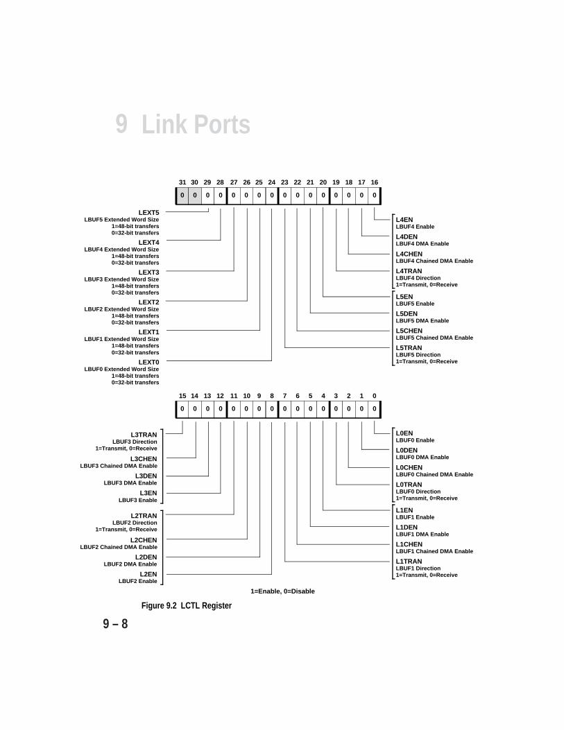
9 Link Ports
9 – 8
11 10 9 8 7 6 5 4 3 2 1 0
000000000000
15 14 13 12
0000
L0ENLBUF0 Enable
1=Enable, 0=Disable
L0DENLBUF0 DMA Enable
L0CHENLBUF0 Chained DMA Enable
L0TRANLBUF0 Direction1=Transmit, 0=Receive
L1ENLBUF1 Enable
L1DENLBUF1 DMA Enable
L1CHENLBUF1 Chained DMA Enable
L1TRANLBUF1 Direction1=Transmit, 0=Receive
L3ENLBUF3 Enable
L3DENLBUF3 DMA Enable
L3CHENLBUF3 Chained DMA Enable
L3TRANLBUF3 Direction
1=Transmit, 0=Receive
L2ENLBUF2 Enable
L2DENLBUF2 DMA Enable
L2CHENLBUF2 Chained DMA Enable
L2TRANLBUF2 Direction
1=Transmit, 0=Receive
27 26 25 24 23 22 21 20 19 18 17 16
000000000000
31 30 29 28
0000
L4ENLBUF4 Enable
L4DENLBUF4 DMA Enable
L4CHENLBUF4 Chained DMA Enable
L4TRANLBUF4 Direction1=Transmit, 0=Receive
L5ENLBUF5 Enable
L5DENLBUF5 DMA Enable
L5CHENLBUF5 Chained DMA Enable
L5TRANLBUF5 Direction1=Transmit, 0=ReceiveLEXT0
LBUF0 Extended Word Size1=48-bit transfers0=32-bit transfers
LEXT1LBUF1 Extended Word Size
1=48-bit transfers0=32-bit transfers
LEXT2LBUF2 Extended Word Size
1=48-bit transfers0=32-bit transfers
LEXT3LBUF3 Extended Word Size
1=48-bit transfers0=32-bit transfers
LEXT4LBUF4 Extended Word Size
1=48-bit transfers0=32-bit transfers
LEXT5LBUF5 Extended Word Size
1=48-bit transfers0=32-bit transfers
Figure 9.2 LCTL Register

9Link Ports
9 – 9
9.2.2 Link Common Control Register (LCOM)The LCOM register contains status bits, packing status bits, and 2X clockrate bits for each buffer. These bits are listed in Table 9.3.
Bit(s) Name Definition0-1 L0STAT(0:1) Link buffer 0 status: 11=full, 00=empty,10=one word *2-3 L1STAT(0:1) Link buffer 1 status: 11=full, 00=empty,10=one word *4-5 L2STAT(0:1) Link buffer 2 status: 11=full, 00=empty,10=one word *6-7 L3STAT(0:1) Link buffer 3 status: 11=full, 00=empty,10=one word *8-9 L4STAT(0:1) Link buffer 4 status: 11=full, 00=empty,10=one word *10-11 L5STAT(0:1) Link buffer 5 status: 11=full, 00=empty,10=one word *12 LCLKX20 Transfer data at 2X the clock rate on Link Buffer 013 LCLKX21 Transfer data at 2X the clock rate on Link Buffer 114 LCLKX22 Transfer data at 2X the clock rate on Link Buffer 215 LCLKX23 Transfer data at 2X the clock rate on Link Buffer 316 LCLKX24 Transfer data at 2X the clock rate on Link Buffer 417 LCLKX25 Transfer data at 2X the clock rate on Link Buffer 518 L2DDMA** Enable 2-dimensional DMA19 LPDRD** Disable internal pulldown resistor for LxCLK and LxACK20 LMSP** Mesh multiprocessing enable (set to 0 for normal operation)21-22 LPATHD** Mesh multiprocessing LPATH changeover delay:
00=no additional delay, 01=1 additional delay,10=2 additional delays, 11=3 additional delays
23-25 reserved26 LRERR0 Receive pack error status for Link Buffer 0:
1=incomplete, 0=complete27 LRERR1 Receive pack error status for Link Buffer 1:
1=incomplete, 0=complete28 LRERR2 Receive pack error status for Link Buffer 2:
1=incomplete, 0=complete29 LRERR3 Receive pack error status for Link Buffer 3:
1=incomplete, 0=complete30 LRERR4 Receive pack error status for Link Buffer 4:
1=incomplete, 0=complete31 LRERR5 Receive pack error status for Link Buffer 5:
1=incomplete, 0=complete
Table 9.3 Link Common Control Register (LCOM)Status bits are read-only.* The code 01 does not appear as a valid status.** Common to all link ports.

9 Link Ports
9 – 10
LCOM Control Bits:
LxSTAT(0:1) When transmitting, these status bits indicate whether there is roomin the buffer for more data. When receiving, these status bits indicatewhether new (unread) data is available in the receive buffer.LxSTAT(1)=1 if there is data in the buffer. LxSTAT(0)=0 if there isroom in the buffer. These bits are read-only. They are cleared whenLxEN changes from 1 to 0. They may subsequently change statewhen the data buffer is read or written.
LCLKX2x This specifies link buffers to transfer at twice the ADSP-2106x clockrate. If LCLKX2x=0, transmit transfers occur at the ADSP-2106xclock frequency, and receive transfers occur at (up to) the ADSP-2106x clock frequency. Set LCLKX2x=1 for receive transfersoccurring at greater than the ADSP-2106x clock frequency.
L2DDMA This directs the DMA controller to address memory as a two-dimensional array as specified in the DMA address registers. OnlyDMA channels 0-5 support 2D DMA. Link buffers 4 and 5 on DMAchannels 6 and 7 do not support 2D DMA.
LPDRD Disables pulldown resistors on signals for unassigned link ports (or onassigned link ports that have their link buffers disabled). These pulldownresistors are 50 kΩ and apply to the LxACK, LxCLK, and LxDAT3-0 signals.Enabling these pulldown resistors keeps the unassigned link port in aninactive state when accessed by another link port. In an applicationwhere several ADSP-2106xs share a link port, only one ADSP-2106xshould have this bit cleared during operation to prevent too manypulldowns on these lines. External resistors may be used in place ofthese if needed. LxACK, LxCLK, and LxDAT3-0 should never be leftunconnected unless the internal pulldowns are enabled.
LMSP Enables mesh multiprocessing mode. Set LMSP=0 for normaloperation.
LPATHD In a mesh multiprocessing application, these bits allow 1, 2 or 3additional clock delays to be inserted before changing to the nextLPATH register. This allows the current receive operation tocomplete on the current link port before a new link port is selected.In some mesh multiprocessing applications, this completion delay issignificant.
LRERRx These bits reflects the status of the receive nibble packer for each linkbuffer. LRERRx will equal 0 when the nibble packer is set to startreceiving a new word. Otherwise it will be 1. If this bit is equal to 1after a word is received, then an error has occurred (e.g. clock glitch).The LRERRx bits are cleared when LxEN changes from 1 to 0. Theymay subsequently change state when the link buffer is read orwritten or while a word is being received.
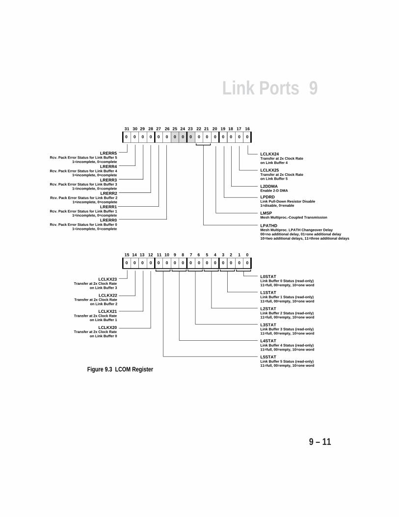
9Link Ports
9 – 11
11 10 9 8 7 6 5 4 3 2 1 0
000000000000
15 14 13 12
0000
26 25 24 23 22 21 20 19 18 17
000000000000
31 30 29 28 27
0000
16
L0STATLink Buffer 0 Status (read-only)11=full, 00=empty, 10=one word
L1STATLink Buffer 1 Status (read-only)11=full, 00=empty, 10=one word
L2STATLink Buffer 2 Status (read-only)11=full, 00=empty, 10=one word
L3STATLink Buffer 3 Status (read-only)11=full, 00=empty, 10=one word
L4STATLink Buffer 4 Status (read-only)11=full, 00=empty, 10=one word
L5STATLink Buffer 5 Status (read-only)11=full, 00=empty, 10=one word
LCLKX23Transfer at 2x Clock Rate
on Link Buffer 3
LCLKX22Transfer at 2x Clock Rate
on Link Buffer 2
LCLKX21Transfer at 2x Clock Rate
on Link Buffer 1
LCLKX20Transfer at 2x Clock Rate
on Link Buffer 0
LPATHDMesh Multiproc. LPATH Changeover Delay00=no additional delay, 01=one additional delay10=two additional delays, 11=three additional delays
LCLKX24Transfer at 2x Clock Rate on Link Buffer 4
LCLKX25Transfer at 2x Clock Rate on Link Buffer 5
L2DDMAEnable 2-D DMA
LPDRDLink Pull-Down Resistor Disable1=disable, 0=enable
LMSPMesh Multiproc.-Coupled Transmission
LRERR5Rcv. Pack Error Status for Link Buffer 5
1=incomplete, 0=completeLRERR4
Rcv. Pack Error Status for Link Buffer 41=incomplete, 0=complete
LRERR3Rcv. Pack Error Status for Link Buffer 3
1=incomplete, 0=completeLRERR2
Rcv. Pack Error Status for Link Buffer 21=incomplete, 0=complete
LRERR1Rcv. Pack Error Status for Link Buffer 1
1=incomplete, 0=completeLRERR0
Rcv. Pack Error Status for Link Buffer 01=incomplete, 0=complete
Figure 9.3 LCOM Register

9 Link Ports
9 – 12
9.2.3 Link Assignment Register (LAR)Each link port is assigned to a link buffer by a 3-bit group in theLink Assignment Register (LAR). There are 6 such groups, one for eachbuffer, as shown in Table 9.4. The LAR can be thought of asperforming a logical (i.e. the link buffer) to physical (i.e. the link port)mapping.
Bits Name Description0-2 A0LB* Link port assignment for LBUF03-5 A1LB* Link port assignment for LBUF16-8 A2LB* Link port assignment for LBUF29-11 A3LB* Link port assignment for LBUF312-14 A4LB* Link port assignment for LBUF415-17 A5LB* Link port assignment for LBUF518-31 reserved (must be set to 0)
Table 9.4 Link Assignment Register (LAR)
* AxLB Link Port #000 Link Port 0001 Link Port 1010 Link Port 2011 Link Port 3100 Link Port 4101 Link Port 5110 reserved111 inactive buffer
The AxLB bits assign a link port to the link buffer x. A link port isDISABLED if it has no buffers assigned or if the link port’s assignedbuffers are disabled. When a link port is disabled, its LxDAT3-0,LxCLK, and LxACK pins are three-stated. If a buffer is intended to beinactive, the corresponding link port assignment field should be set to7.
Memory-to-memory transfers may be accomplished by assigning thesame link port to two buffers, disabling the port partially. One buffertransmits while the other receives. Up to three memory-to memorytransfers may occur simultaneously, by using all six link buffers. Thispartially disabled mode is known as loopback mode. Using thisconfiguration, LxDAT3-0 and LxACK will not be driven or sensed andLxCLK will not be driven. However, LxCLK should not be drivenexternally in this mode, due to the fact that an LxCLK transition maybe sensed and result in a nibble shift in the received data buffer.
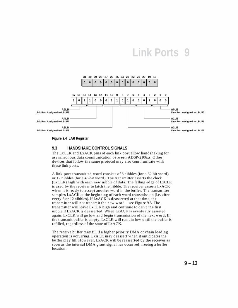
9Link Ports
9 – 13
11 10 9 8 7 6 5 4 3 2 1 0
000100010110
15 14 13 12
0011
26 25 24 23 22 21 20 19 18
0000000000
31 30 29 28 27
0000
A0LBLink Port Assigned to LBUF0
17 16
01
A1LBLink Port Assigned to LBUF1
A2LBLink Port Assigned to LBUF2
A5LBLink Port Assigned to LBUF5
A4LBLink Port Assigned to LBUF4
A3LBLink Port Assigned to LBUF3
Figure 9.4 LAR Register
9.3 HANDSHAKE CONTROL SIGNALSThe LxCLK and LxACK pins of each link port allow handshaking forasynchronous data communication between ADSP-2106xs. Otherdevices that follow the same protocol may also communicate withthese link ports.
A link-port-transmitted word consists of 8 nibbles (for a 32-bit word)or 12 nibbles (for a 48-bit word). The transmitter asserts the clock(LxCLK) high with each new nibble of data. The falling edge of LxCLKis used by the receiver to latch the nibble. The receiver asserts LxACKwhen it is ready to accept another word in the buffer. The transmittersamples LxACK at the beginning of each word transmission (i.e. afterevery 8 or 12 nibbles). If LxACK is deasserted at that time, thetransmitter will not transmit the new word—see Figure 9.5. Thetransmitter will leave LxCLK high and continue to drive the firstnibble if LxACK is deasserted. When LxACK is eventually assertedagain, LxCLK will go low and begin transmission of the next word. Ifthe transmit buffer is empty, LxCLK will remain low until the buffer isrefilled, regardless of the state of LxACK.
The receive buffer may fill if a higher priority DMA or chain loadingoperation is occurring. LxACK may deassert when it anticipates thebuffer may fill. However, LxACK will be reasserted by the receiver assoon as the internal DMA grant signal has occurred, freeing a bufferlocation.
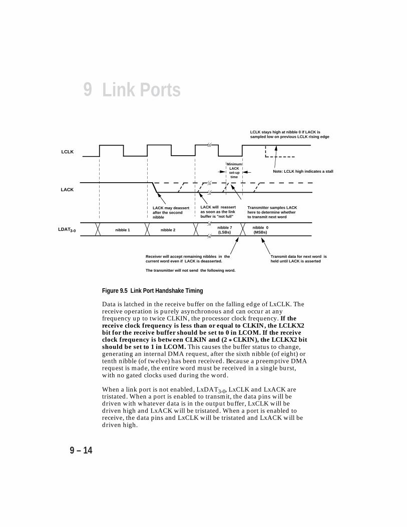
9 Link Ports
9 – 14
Figure 9.5 Link Port Handshake Timing
Data is latched in the receive buffer on the falling edge of LxCLK. Thereceive operation is purely asynchronous and can occur at anyfrequency up to twice CLKIN, the processor clock frequency. If thereceive clock frequency is less than or equal to CLKIN, the LCLKX2bit for the receive buffer should be set to 0 in LCOM. If the receiveclock frequency is between CLKIN and (2 * CLKIN), the LCLKX2 bitshould be set to 1 in LCOM. This causes the buffer status to change,generating an internal DMA request, after the sixth nibble (of eight) ortenth nibble (of twelve) has been received. Because a preemptive DMArequest is made, the entire word must be received in a single burst,with no gated clocks used during the word.
When a link port is not enabled, LxDAT3-0, LxCLK and LxACK aretristated. When a port is enabled to transmit, the data pins will bedriven with whatever data is in the output buffer, LxCLK will bedriven high and LxACK will be tristated. When a port is enabled toreceive, the data pins and LxCLK will be tristated and LxACK will bedriven high.
LCLK
nibble 1 nibble 2nibble 0 (MSBs)
LACK
Transmitter samples LACK here to determine whether to transmit next word
nibble 7(LSBs)
Receiver will accept remaining nibbles in the current word even if LACK is deasserted.
The transmitter will not send the following word.
Transmit data for next word is held until LACK is asserted
Note: LCLK high indicates a stall
LDAT3-0
MinimumLACK set-up time
LACK may deassert after the second nibble
LCLK stays high at nibble 0 if LACK is sampled low on previous LCLK rising edge
LACK will reassert as soon as the link buffer is "not full"
9Link Ports
9 – 15
To allow a transmitter and a receiver to be enabled (assigned and linkbuffer enabled) at different times, LxACK, LxCLK, and LxDAT3-0 maybe held low with the 50 kΩ internal pulldown resistors if LPDRD iscleared when the link port is disabled. Thus, if the transmitter isenabled before the receiver, LxACK will be low and the transmission isheld off. Similarly, if the receiver is enabled before the transmitter,LxCLK will be held low and the receiver will be held off. If many linkports are bused together, one external resistor should be used to pulldown each bused line instead of the internal pulldowns. This willguarantee that the bused lines are not pulled down too strongly.
LxACK, LxCLK, and LxDAT3-0 should not be left unconnected unlessexternal pulldown resistors or the internal pulldowns are used.
9.4 LINK BUFFERSEach link buffer consists of an external and an internal register (seeFigure 9.1). When transmitting, the internal register is used to acceptthe DMA data from internal memory. The external register performsthe unpacking for the link port, most significant nibble first. These tworegisters form a two-stage FIFO, the LBUFx buffer. Two words can bewritten into the register (by DMA or from the core) before it signals afull condition. As each word is unpacked and transmitted, the nextlocation in the FIFO becomes available and a new DMA request ismade. If the register becomes empty, the LxCLK signal will bedeasserted.
Full/empty status for the link buffer FIFOs is given by the LxSTAT bitsof the LCOM register. This status is cleared for a link buffer when itsLxEN enable bit is cleared in the LCTL register.
During receiving, the external buffer is used to pack the receive portdata (most significant nibble first) and pass it to the internal registerbefore DMA-transferring it to internal memory. This buffer is a two-deep FIFO. If the ADSP-2106x’s DMA controller does not service itbefore both locations are filled, then the LxACK signal will bedeasserted.
The link buffer width may be selected to be either 32 or 48 bits. Thisselection is made individually for each buffer with the LEXT bits in theLCTL register. For 40-bit extended precision data or 48-bit instructiontransfers, the width must be set to 48 bits.
9 Link Ports
9 – 16
9.4.1 Core Processor Access To Link BuffersIn applications where the latency of link port DMA transfers to andfrom internal memory is too long, or where a process is continuousand has no block boundaries, the ADSP-2106x processor core may reador write link buffers directly using the full/empty status bit of the linkbuffer to automatically pace the operation. The full or empty status of aparticular LBUFx buffer can be determined by reading the LCOMcontrol/status register. DMA should be disabled (i.e. the LxDEN bitshould be cleared) when using this capability. A programmingexample of core-driven transfers is shown at the end of this chapter.
If a read is attempted from an empty receive buffer, the core will hanguntil the link port completes transmission of a word. Similarly, if awrite is attempted to a full transmit buffer, the core will hang until theexternal device accepts the complete word. Up to four words (2 in thereceiver and 2 in the transmitter) may be sent without a hang beforethe receiver core must read a link buffer register. To prevent this typeof hang condition from occurring, the BHD (Buffer Hang Disable) bitcan be set in the SYSCON register.
9.4.2 Host Processor Access To Link BuffersThe link buffers can also be accessed by the external host processor,using direct reads and writes. When the host reads or writes to thesebuffers, the word width is determined only by the host packing mode,as selected by the HPM bits in the SYSCON register, and not by theLEXT bit in LCTL.
9.5 LINK PORT DMA CHANNELSLink buffers 0-5 are supported by DMA channels 1, 3, 4, 5, 6, and 7respectively. Some DMA channels are dedicated and others are shared:
• DMA channel 1 is shared by SPORT1 receive and link buffer 0 (LBUF0).• DMA channel 3 is shared by SPORT1 transmit and link buffer 1 (LBUF1).• DMA channel 4 is dedicated to link buffer 2 (LBUF2).• DMA channel 5 is dedicated to link buffer 3 (LBUF3).• DMA channel 6 is shared by ext. port buffer 0 (EPB0) and link buffer 4.• DMA channel 7 is shared by ext. port buffer 1 (EPB1) and link buffer 5.

9Link Ports
9 – 17
DMA Channels 1 and 3 are shared by link buffers 0 and 1, respectively,and by SPORT1. This has several functional implications:
• If the SPORT1 receive DMA enable bit or chaining enable bit is set, thenSPORT1 receive is assigned DMA channel 1.
• If the LBUF0 DMA enable bit is set, then link buffer 0 is assigned thisDMA channel.
• If both enables are set, the SPORT is selected.
• If neither the SPORT DMA enable or LBUF0 DMA enable is set, theninterrupts from both buffers are ORed.
SPORT1 transmit and LBUF1 are shared and selected in the same way.
DMA Channel 6 is shared by the external port buffer EPB0 and linkbuffer 4 (LBUF4). Functional implications include:
• If the EPB0 DMA enable bit or chaining enable bit is set, then EPB0 isassigned DMA channel 6.
• If the LBUF4 DMA enable bit is set, then link buffer 4 is assigned thisDMA channel.
• If both enables are set, EPB0 is selected.
• If neither the external port DMA enable or LBUF4 DMA enable is set,then interrupts from both buffers are ORed.
EPB1 and LBUF5 share DMA channel 7 and are selected in the sameway.
A maskable interrupt is generated when the DMA block transfer hascompleted. A more complete discussion on interrupts can be found inthe “Link Port Interrupts” section of this chapter.
If DMA is disabled for a buffer, then the buffer may be read or writtenby the core processor as a memory-mapped location. A maskableinterrupt is generated while DMA is disabled and the receive buffer isnot empty or if the transmit buffer is not full.
9 Link Ports
9 – 18
9.5.1 DMA Chaining For Link PortsIn chained DMA operations, the ADSP-2106x automatically sets upanother DMA transfer when the contents of the current buffer havebeen transmitted (or received). The chain pointer register (CPx) is usedto point to the next set of buffer parameters stored in memory. TheADSP-2106x’s DMA controller automatically downloads these bufferparameters to set up the next DMA sequence. Refer to the DMAchapter of this manual for details on how to set up chainingparameters in memory.
DMA chaining is enabled on each link port by setting the LxCHEN bitin LCTL. When chaining is enabled, DMA transfers are initiated bywriting a memory address to the CP register.
Six DMA parameter registers are initialized for the chained operation,in the following order:
IIx Index (start address of memory buffer)IMx Modify (increment)Cx CountCPx Chain Pointer
9.6 LINK PORT INTERRUPTSLink ports have 3 different types of interrupts:
1. nterrupts caused by the received or transmitted data when the ADSP-2106x core is accessing the buffers directly and DMA is not enabled.
2. Interrupts generated by the completion of a DMA cycle.3. Interrupts caused by an attempted external access of a link port that is
unassigned or assigned to a link buffer that is not enabled.
Types 1 and 2 are mutually exclusive and use the same interrupt.Type 3 is independent of 1 and 2 and uses a different interrupt vector.Details of each kind of interrupt follow below.
9.6.1 Link Port Interrupts With DMA DisabledIf DMA is disabled for a link port buffer, then the buffer may bewritten or read by the ADSP-2106x core as a memory-mapped IOPregister.
9Link Ports
9 – 19
If the DMA is disabled but the associated link buffer is enabled, then amaskable interrupt is generated whenever a receive buffer is notempty or when a transmit buffer is not full.
The interrupt latch bit in IRPTL may be masked in the correspondingIMASK register bit. When initially enabling the IMASK bit, thecorresponding bit in IRPTL should be cleared first to clear out anyrequest that may have been inadvertently latched.
The interrupt service routine should test the buffer status after eachread or write to check when the buffer is empty or full, in order todetermine when it should return from interrupt. This will reduce thenumber of interrupts it must service.
9.6.2 Link Port Interrupts With DMA EnabledA link port interrupt is generated when the DMA operation is done—i.e. when the block transfer has completed and the DMA count registeris zero.
There is an option for implementing a protocol to send additionalcontrol information at the end of a block transfer. Because the receiveDMA buffer is empty when the DMA block has completed, theexternal bus master can send up to two additional words to the slaveADSP-2106x’s buffer which has space for the two words. The slave’sDMA done interrupt service routine could then read the buffer and usethese control words to determine the next course of action.
9.6.3 Link Port Service Request Interrupts (LSRQ)Link port service requests allow a disabled (unassigned or assignedand buffer disabled) link port to cause an interrupt when an externalaccess is attempted. The transmit and receive request status bits of theLSRQ register (bits 20-31) allow an ADSP-2106x to determine ifanother ADSP-2106x is attempting to send or receive data through aparticular link port. This lets two processors comunicate without priorknowledge of the transfer direction, link port number, or exactly whenthe transfer is to occur.
When LxACK or LxCLK is asserted externally, a link service request(LSR) is generated in a disabled (unassigned or assigned and bufferdisabled) link port. LSRs will not be generated for a link port that isdisabled by loopback mode. Each LSR is gated by mask bits before
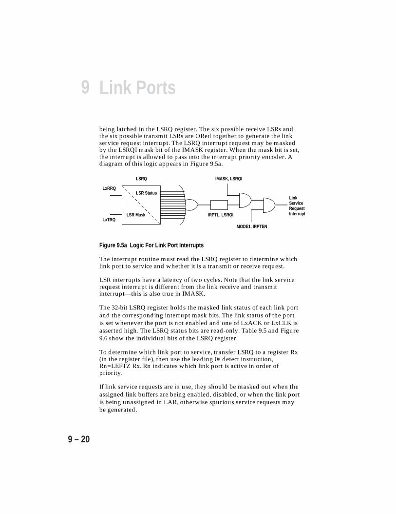
9 Link Ports
9 – 20
being latched in the LSRQ register. The six possible receive LSRs andthe six possible transmit LSRs are ORed together to generate the linkservice request interrupt. The LSRQ interrupt request may be maskedby the LSRQI mask bit of the IMASK register. When the mask bit is set,the interrupt is allowed to pass into the interrupt priority encoder. Adiagram of this logic appears in Figure 9.5a.
LxRRQ
LxTRQLSR Mask
LSR Status
LSRQ
IRPTL, LSRQI
MODE1, IRPTEN
IMASK, LSRQI
Link Service Request Interrupt
Figure 9.5a Logic For Link Port Interrupts
The interrupt routine must read the LSRQ register to determine whichlink port to service and whether it is a transmit or receive request.
LSR interrupts have a latency of two cycles. Note that the link servicerequest interrupt is different from the link receive and transmitinterrupt—this is also true in IMASK.
The 32-bit LSRQ register holds the masked link status of each link portand the corresponding interrupt mask bits. The link status of the portis set whenever the port is not enabled and one of LxACK or LxCLK isasserted high. The LSRQ status bits are read-only. Table 9.5 and Figure9.6 show the individual bits of the LSRQ register.
To determine which link port to service, transfer LSRQ to a register Rx(in the register file), then use the leading 0s detect instruction,Rn=LEFTZ Rx. Rn indicates which link port is active in order ofpriority.
If link service requests are in use, they should be masked out when theassigned link buffers are being enabled, disabled, or when the link portis being unassigned in LAR, otherwise spurious service requests maybe generated.

9Link Ports
9 – 21
This need for masking is due to a delay before LxCLK or LxACK (ifalready asserted) signals are pulled (if pulldowns enabled) or drivenexternally (if pulldowns disabled) below logic threshold. During thisdelay, these signals are sampled asserted and generate an LSRQ.
To avoid the possiblity of spurious interrupts, mask the LSRQinterrupt or the appropriate request bit in the LSRQ register and allowan appropriate delay before unmasking. Alternatively, mask the LSRQinterrupt and poll the appropriate request status bit until it is clearedand then unmask the interrupt.
Bit Name Description0-3 reserved4 L0TM Link Port 0 transmit mask5 L0RM Link Port 0 receive mask6 L1TM Link Port 1 transmit mask7 L1RM Link Port 1 receive mask8 L2TM Link Port 2 transmit mask9 L2RM Link Port 2 receive mask10 L3TM Link Port 3 transmit mask11 L3RM Link Port 3 receive mask12 L4TM Link Port 4 transmit mask13 L4RM Link Port 4 receive mask14 L5TM Link Port 5 transmit mask15 L5RM Link Port 5 receive mask16-19 reserved20 L0TRQ Link Port 0 transmit request status (read-only)21 L0RRQ Link Port 0 receive request status (read-only)22 L1TRQ Link Port 1 transmit request status (read-only)23 L1RRQ Link Port 1 receive request status (read-only)24 L2TRQ Link Port 2 transmit request status (read-only)25 L2RRQ Link Port 2 receive request status (read-only)26 L3TRQ Link Port 3 transmit request status (read-only)27 L3RRQ Link Port 3 receive request status (read-only)28 L4TRQ Link Port 4 transmit request status (read-only)29 L4RRQ Link Port 4 receive request status (read-only)30 L5TRQ Link Port 5 transmit request status (read-only)31 L5RRQ Link Port 5 receive request status (read-only)
Table 9.5 Link Service Request Register (LSRQ)
For transmit request status bits, LxTRQ=1 means LxACK=1, LxTM=1, and LxEN=0.For receive request status bits, LxRRQ=1 means LxCLK=1, LxRM=1, and LxEN=0.

9 Link Ports
9 – 22
27 26 25 24 23 22 21 20 19 18 17 1631 30 29 28
11 10 9 8 7 6 5 4 3 2 1 0
000000000000
15 14 13 12
0000
L0TMLink Port 0 Transmit Mask
L0RMLink Port 0 Receive Mask
L1TMLink Port 1 Transmit Mask
L1RMLink Port 1 Receive Mask
L2TMLink Port 2 Transmit Mask
L2RMLink Port 2 Receive Mask
L3RMLink Port 3 Receive Mask
L3TMLink Port 3 Transmit Mask
L4RMLink Port 4 Receive Mask
L4TMLink Port 4 Transmit Mask
L5RMLink Port 5 Receive Mask
L5TMLink Port 5 Transmit Mask
0000000000000000
L0TRQLink Port 0 Transmit Request
L0RRQLink Port 0 Receive Request
L1TRQLink Port 1 Transmit Request
L1RRQLink Port 1 Receive Request
L2TRQLink Port 2 Transmit Request
L2RRQLink Port 2 Receive Request
L3RRQLink Port 3 Receive Request
L3TRQLink Port 3 Transmit Request
L4RRQLink Port 4 Receive Request
L4TRQLink Port 4 Transmit Request
L5RRQLink Port 5 Receive Request
L5TRQLink Port 5 Transmit Request
Request Bits are Read-Only Status
Figure 9.6 LSRQ Register
For transmit request status bits, LxTRQ=1 means LxACK=1, LxTM=1, and LxEN=0.For receive request status bits, LxRRQ=1 means LxCLK=1, LxRM=1, and LxEN=0.
9Link Ports
9 – 23
9.7 TRANSMISSION ERROR DETECTIONTransmission errors on the link ports may be detected by reading theLRERRx bits in the LCOM register. These bits reflects the status of eachnibble counter. The LRERRx bit will be zero if the pack counter of thecorresponding link buffer is zero (i.e. a multiple of 8 or 12 nibbles havebeen received). If LRERR is high when a transmission has completed,then an error occurred during transmission. (Note that the DMA wordcount provides an exact count of the number of words to betransferred.)
To allow checking of this status, the transmitter and receiver shouldfollow a protocol such as the one described below:
Transmitter Protocol—To make use of the LRERRx status, oneadditional dummy word should always be transmitted at the end of ablock transmission. The transmitter must then deselect the link port toallow the receiver to send an appropriate message back to thetransmitter.
Receiver Protocol—When the receiver has received the data block,indicated by a DMA done interrupt, it checks that it has received anadditional word in the link buffer and then reads the LRERR bit. Thereceiver may then clear the link buffer (LxEN=0) and transmit theappropriate message back to the transmitter on the same, or adifferent, link port.
9.8 TOKEN PASSINGTwo processors wishing to communicate on a link port need to knowwhich of them is currently the transmitter and which is the receiver,otherwise they might both try to transmit at the same time. Tokenpassing is a way of accomplishing this. Figure 9.7 shows a flow chart ofthe token passing process.
Token passing is a way of establishing which of two ADSP-2106xs isthe current transmitter. The token is a software flag, similar to asemaphore, that is passed between the processors. At reset, byconvention, the token (flag) is set to reside in the link port of onedevice, making him the master and the transmitter. When a receiverlink port (slave) wants to become the master, he may assert his LxACKline (request data) to get the master’s attention. The master will know,through software protocol, whether he is supposed to respond withactual data or whether he is being asked for the token.
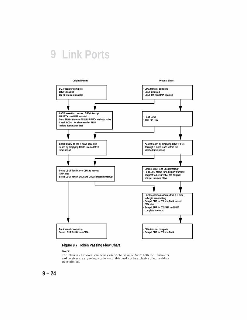
9 Link Ports
9 – 24
Figure 9.7 Token Passing Flow ChartNotes:The token release word can be any user-defined value. Since both the transmitterand receiver are expecting a code word, this need not be exclusive of normal datatransmission.
Original Master Original Slave
• DMA transfer complete• LBUF disabled• LSRQ interrupt enabled
• DMA transfer complete• LBUF disabled• LBUF RX non-DMA enabled
• LACK assertion causes LSRQ interrupt• LBUF TX non-DMA enabled• Send TRW 4 times to fill LBUF FIFOs on both sides• Check LCOM for slave read of TRW before acceptance test
• Read LBUF• Test for TRW
• Check LCOM to see if slave accepted token by emptying FIFOs in an allotted time period
• Accept token by emptying LBUF FIFOs through 3 more reads within the allotted time period
• Setup LBUF for RX non-DMA to accept DMA size• Setup LBUF for RX DMA and DMA complete interrupt
• Disable LBUF and LSRQ interrupt• Poll LSRQ status for Link port transmit request to be sure that the original master is now a slave
• DMA transfer complete• Setup LBUF for RX non-DMA
• LACK assertion assures that it is safe to begin transmitting• Setup LBUF for TX non-DMA to send DMA size• Setup LBUF for TX DMA and DMA complete interrupt
• DMA transfer complete• Setup LBUF for TX non-DMA
9Link Ports
9 – 25
If the master wishes to give up the token, he may send back a user-defined token release word and thereafter clear his token flag.Simultaneously, the slave examines the data sent back and if it is thetoken release word, the slave will set his token, and can thereaftertransmit. If the received data is not the token release word, then theslave must assume the master was beginning a new transmission.
Through software protocol, the master can also ask to receive data bysending the token release word without the LxACK (data request)going low first.
An example of software protocol for token passing through the linkports is included at the end of this chapter. Figure 9.7 shows a flowchart of the example code and the following is a description of theprocess:
The example code is to be loaded on both the original master and theoriginal slave. The code is ID intelligent for multiprocessor systems:ID1 is the original master (transmitter) and ID2 is original slave(receiver). The master transmits a buffer via DMA through LPORT0using LBUF3 and the slave receives through LPORT0 using LBUF2.The slave then requests the token by generating an LSRQ interrupt inthe disabled link port of the master (LPORT0). The master responds bysending the token release word and waiting to see if it is accepted. Theslave checks to see that it is the token release word and will accept thetoken by emptying the master’s link buffer FIFO within apredetermined amount of time. If the token is accepted the slave willbecome the master and transmit a buffer of data to the new slave. If thetoken is rejected, the master will transmit a second buffer. Whencomplete, the original master will finish by setting up LBUF2 to receivewithout DMA, and the original slave will set up LBUF3 to transmitwithout DMA.
The following is a list of the major areas of concern whenimplementing a software protocol scheme for token passing:
• Ensure that both link buffers are not enabled to transmit at the sametime. In the event that this is allowed, data may be transmitted and lostdue to the fact that neither link port will be driving LxACK. In theexample provided at the end of the chapter, the LSRQ register statusbits are polled to ensure that the master becomes the slave before theslave becomes the master, thus avoiding the two transmitter conflict.
9 Link Ports
9 – 26
• Ensure that the link interrupt selection matches the application. If astatus detection scheme using the status bits of the LSRQ register is tobe used, it is important to note the following: If a link port that isconfigured to receive is disabled while LxACK is asserted, there will bean RC delay before the 50k ohm pulldown resistor on LxACK (ifenabled) can pull the value below logic threshold. Likewise, if a linkport that is configured to transmit is disabled while LxCLK is asserted,there will be an RC delay before the 50k ohm pulldown resistor onLxCLK (if enabled) can pull the value below logic threshold. If theappropriate request status bit is unmasked in the LSRQ register (in thisinstance), then an LSR will be latched and the LSRQ interrupt may beserviced, even though unintended, if enabled.
• Ensure that synchronization is not disrupted by unrelated influences atcritical sections where timing control loops are used to synchronizeparallel code execution. Disabling of nested interrupts is one of thetechniques used in the example to control this.
9.9 LINK TRANSMISSION LINESThe link ports are designed to allow long distance connections to bemade between the driver and the receiver. This is possible because thelinks are self-synchronizing, i.e. the clock and data are transmittedtogether. Only relative delay, not absolute delay between clock anddata is of importance.
In addition, the LACK signal inhibits transmission of the next word,not of the current nibble (i.e. the current word is always allowed tocomplete transmission). This allows delays of 2 to 3 cycles for theLxACK signal to reach the transmitter.
The links are designed to drive transmission lines with characteristicimpedances of 50Ω or greater. A higher transmission line impedancereduces the on-chip effect of driver impedance variations, for distanceslonger than about 6 inches. It is recommended that an external seriestermination resistor be used at each link port pin to absorb reflectionsfrom the open circuit at the destination. The external resistor should beselected such that its value (plus the internal resistance of the driver)be equal to the characteristic impedance of the transmission line.
Thus, if the typical internal drive resistance is 10Ω and thecharacteristic impedance is 50Ω, then the link port pin resistor shouldbe 40Ω.
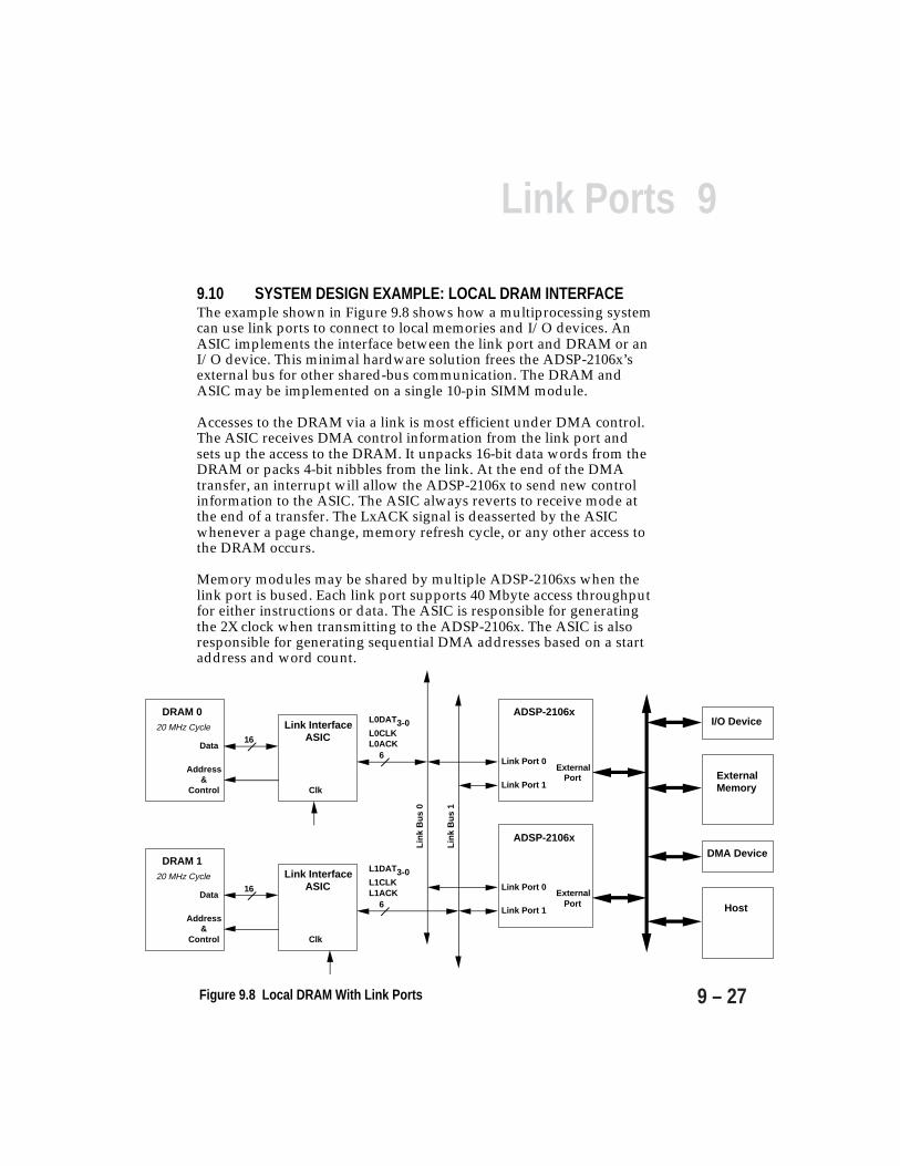
9Link Ports
9 – 27
9.10 SYSTEM DESIGN EXAMPLE: LOCAL DRAM INTERFACEThe example shown in Figure 9.8 shows how a multiprocessing systemcan use link ports to connect to local memories and I/O devices. AnASIC implements the interface between the link port and DRAM or anI/O device. This minimal hardware solution frees the ADSP-2106x’sexternal bus for other shared-bus communication. The DRAM andASIC may be implemented on a single 10-pin SIMM module.
Accesses to the DRAM via a link is most efficient under DMA control.The ASIC receives DMA control information from the link port andsets up the access to the DRAM. It unpacks 16-bit data words from theDRAM or packs 4-bit nibbles from the link. At the end of the DMAtransfer, an interrupt will allow the ADSP-2106x to send new controlinformation to the ASIC. The ASIC always reverts to receive mode atthe end of a transfer. The LxACK signal is deasserted by the ASICwhenever a page change, memory refresh cycle, or any other access tothe DRAM occurs.
Memory modules may be shared by multiple ADSP-2106xs when thelink port is bused. Each link port supports 40 Mbyte access throughputfor either instructions or data. The ASIC is responsible for generatingthe 2X clock when transmitting to the ADSP-2106x. The ASIC is alsoresponsible for generating sequential DMA addresses based on a startaddress and word count.
Figure 9.8 Local DRAM With Link Ports
ADSP-2106x
Link Port 0
Link Port 1
ExternalPort
I/O Device
External Memory
DMA Device
Host
ADSP-2106x
Link Port 0
Link Port 1
ExternalPort
Lin
k B
us
1
Lin
k B
us
0
DRAM 0
Data
Link InterfaceASIC
20 MHz Cycle
Clk
Address&
Control
16
L0DAT3-0L0CLKL0ACK
6
DRAM 1
Data
Link InterfaceASIC
20 MHz Cycle
Clk
Address&
Control
16
L1DAT3-0L1CLKL1ACK
6
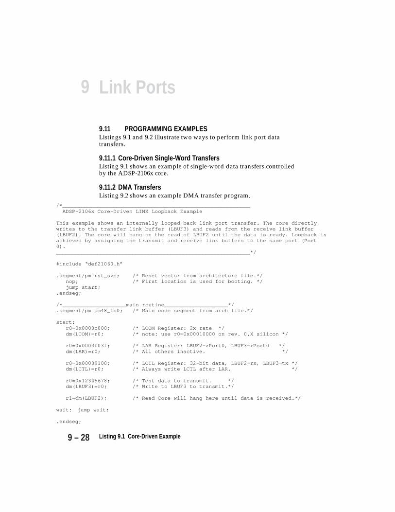
9 Link Ports
9 – 28 Listing 9.1 Core-Driven Example
9.11 PROGRAMMING EXAMPLESListings 9.1 and 9.2 illustrate two ways to perform link port datatransfers.
9.11.1 Core-Driven Single-Word TransfersListing 9.1 shows an example of single-word data transfers controlledby the ADSP-2106x core.
9.11.2 DMA TransfersListing 9.2 shows an example DMA transfer program.
/*___________________________________________________________ ADSP-2106x Core-Driven LINK Loopback Example
This example shows an internally looped-back link port transfer. The core directlywrites to the transfer link buffer (LBUF3) and reads from the receive link buffer(LBUF2). The core will hang on the read of LBUF2 until the data is ready. Loopback isachieved by assigning the transmit and receive link buffers to the same port (Port0)._____________________________________________________________*/
#include “def21060.h”
.segment/pm rst_svc; /* Reset vector from architecture file.*/nop; /* First location is used for booting. */jump start;
.endseg;
/*____________________main routine____________________*/.segment/pm pm48_1b0; /* Main code segment from arch file.*/
start:r0=0x0000c000; /* LCOM Register: 2x rate */dm(LCOM)=r0; /* note: use r0=0x00010000 on rev. 0.X silicon */
r0=0x0003f03f; /* LAR Register: LBUF2->Port0, LBUF3->Port0 */dm(LAR)=r0; /* All others inactive. */
r0=0x00009100; /* LCTL Register: 32-bit data, LBUF2=rx, LBUF3=tx */dm(LCTL)=r0; /* Always write LCTL after LAR. */
r0=0x12345678; /* Test data to transmit. */dm(LBUF3)=r0; /* Write to LBUF3 to transmit.*/
r1=dm(LBUF2); /* Read—Core will hang here until data is received.*/
wait: jump wait;
.endseg;

9Link Ports
9 – 29
/*_______________________________________________________________ ADSP-2106x DMA-Driven LINK Loopback Example
This example shows an internally looped-back link port transfer.Two DMA channels are used. Link buffer 3 (LBUF3) and correspondingDMA channel 5 is used for transmit. Link buffer 2 (LBUF2) andcorresponding DMA channel 5 is used for receive. The LBUF2 interruptwill occur when the DMA transfer is complete. Loopback is achievedby assigning the transmit and receive link buffers to thesame port (Port 0)._______________________________________________________________*/
#define N 8#include “def21060.h”
.segment/dm dm32_b1; /* Data segment name described in arch. file.*/
.var source[N] = 0x11111111, 0x22222222, 0x33333333, 0x44444444, 0x55555555, 0x66666666, 0x77777777, 0x88888888;.var destination[N];.endseg;
.segment/pm rst_svc; /* Reset vector from arch. file. */nop; /* First location is used for booting.*/jump start;
.endseg;
.segment/pm lp2_svc; /* Link buffer 2 interrupt vector.*/jump lp2rx;
.endseg;
/*____________________main routine____________________*/
.segment/pm pm48_1b0; /* Main code segment from arch. file.*/
start:r0=source;dm(II5)=r0; /* Set DMA tx index to start of source buffer.*/r0=destination;dm(II4)=r0; /* Set DMA rx index to start of destination buffer.*/r0=1;dm(IM5)=r0; /* Set DMA modify (stride) to 1.*/dm(IM4)=r0;r0=@source;dm(C5)=r0; /* Set DMA count to length of data buffer.*/dm(C4)=r0;
r0=0x0000c000; /* LCOM Register: 2x rate */dm(LCOM)=r0; /* note: use r0=0x00010000 on rev. 0.X silicon */
(listing continues on next page)
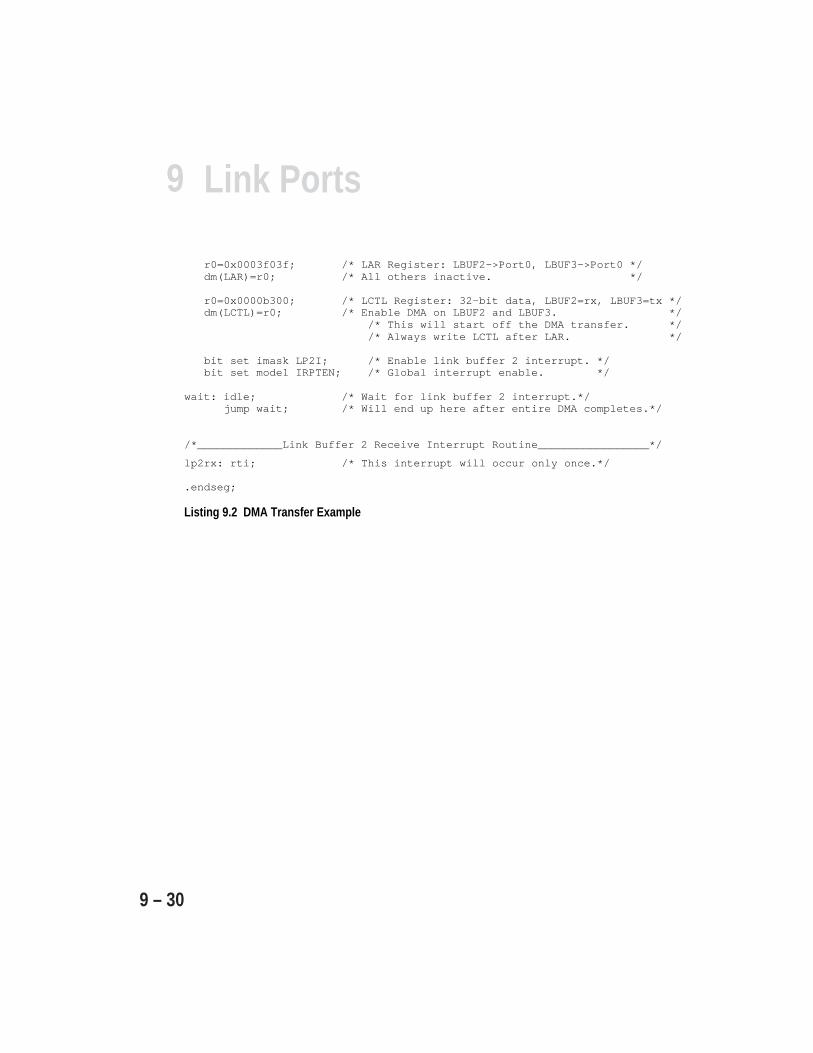
9 Link Ports
9 – 30
r0=0x0003f03f; /* LAR Register: LBUF2->Port0, LBUF3->Port0 */dm(LAR)=r0; /* All others inactive. */
r0=0x0000b300; /* LCTL Register: 32-bit data, LBUF2=rx, LBUF3=tx */dm(LCTL)=r0; /* Enable DMA on LBUF2 and LBUF3. */
/* This will start off the DMA transfer. */ /* Always write LCTL after LAR. */
bit set imask LP2I; /* Enable link buffer 2 interrupt. */bit set mode1 IRPTEN; /* Global interrupt enable. */
wait: idle; /* Wait for link buffer 2 interrupt.*/ jump wait; /* Will end up here after entire DMA completes.*/
/*_____________Link Buffer 2 Receive Interrupt Routine_________________*/
lp2rx: rti; /* This interrupt will occur only once.*/
.endseg;
Listing 9.2 DMA Transfer Example

9Link Ports
9 – 31
/*_____________________________________________________________________________ADSP-2106x LINK Token Pass Example
This is an example of software protocol for token ring passing through the linkports using LSRQ. This code is to be loaded on both the original master and theoriginal slave. The code is ID intelligent for multiprocessor systems: ID1 isthe original master (transmitter) and ID2 is original slave (receiver). Themaster transmits a buffer via dma through LPORT0 using LBUF3 and the slavereceives through LPORT0 using LBUF2. The slave then requests the token bygenerating an LSRQ interrupt in the disabled link port of the master (LPORT0).The master responds by sending the token release word and waiting to see if itis accepted. The slave checks to see that it is the token release word and willaccept the token by emptying the master’s link buffer FIFO within apredetermined amount of time. If the token is accepted the slave will becomethe master and transmit a buffer of data to the new slave. If the token isrejected, the master will transmit a second buffer. When complete the originalmaster will finish by setting up LBUF2 to receive without DMA and the originalslave will set up LBUF3 to transmit without DMA. FLAG0 is used as a softwareflac to indicate the original master.________________________________________________________________________________*/
#include “def21060.h”
#define N 8 /* Size of buffer */
#define trw 0x0 /* Token release word */
#define orig_master_id 1 /* ID of SHARC to be original master */#define orig_slave_id 2 /* ID of SHARC to be original slave */
.SEGMENT/DM dm_data;
.var source_1[N]= 0x11111111, 0x22222222, 0x33333333, 0x44444444, 0x11111111, 0x22222222, 0x33333333, 0x44444444;
.var source_2[N]= 0x55555555, 0x66666666, 0x77777777, 0x88888888, 0x55555555, 0x66666666, 0x77777777, 0x88888888;
Listing 9.3 Link Token Passing Example (continues)
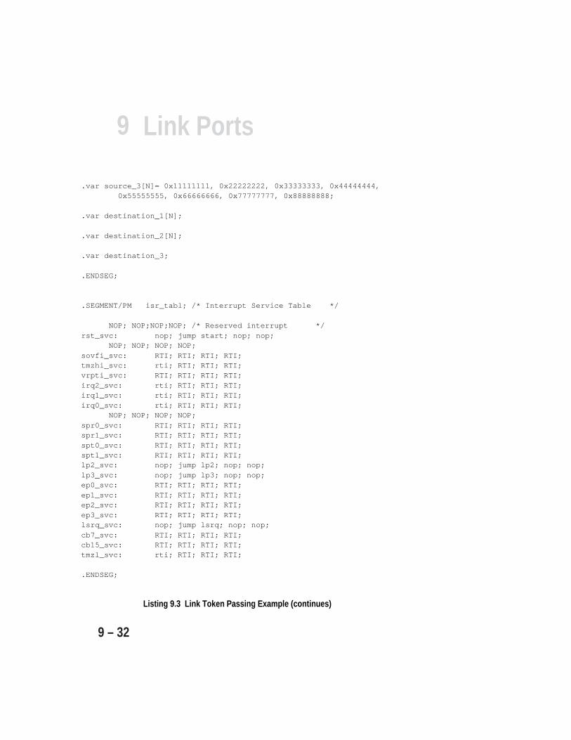
9 Link Ports
9 – 32
.var source_3[N]= 0x11111111, 0x22222222, 0x33333333, 0x44444444, 0x55555555, 0x66666666, 0x77777777, 0x88888888;
.var destination_1[N];
.var destination_2[N];
.var destination_3;
.ENDSEG;
.SEGMENT/PM isr_tabl; /* Interrupt Service Table */
NOP; NOP;NOP;NOP; /* Reserved interrupt */rst_svc: nop; jump start; nop; nop;
NOP; NOP; NOP; NOP;sovfi_svc: RTI; RTI; RTI; RTI;tmzhi_svc: rti; RTI; RTI; RTI;vrpti_svc: RTI; RTI; RTI; RTI;irq2_svc: rti; RTI; RTI; RTI;irq1_svc: rti; RTI; RTI; RTI;irq0_svc: rti; RTI; RTI; RTI;
NOP; NOP; NOP; NOP;spr0_svc: RTI; RTI; RTI; RTI;spr1_svc: RTI; RTI; RTI; RTI;spt0_svc: RTI; RTI; RTI; RTI;spt1_svc: RTI; RTI; RTI; RTI;lp2_svc: nop; jump lp2; nop; nop;lp3_svc: nop; jump lp3; nop; nop;ep0_svc: RTI; RTI; RTI; RTI;ep1_svc: RTI; RTI; RTI; RTI;ep2_svc: RTI; RTI; RTI; RTI;ep3_svc: RTI; RTI; RTI; RTI;lsrq_svc: nop; jump lsrq; nop; nop;cb7_svc: RTI; RTI; RTI; RTI;cb15_svc: RTI; RTI; RTI; RTI;tmzl_svc: rti; RTI; RTI; RTI;
.ENDSEG;
Listing 9.3 Link Token Passing Example (continues)
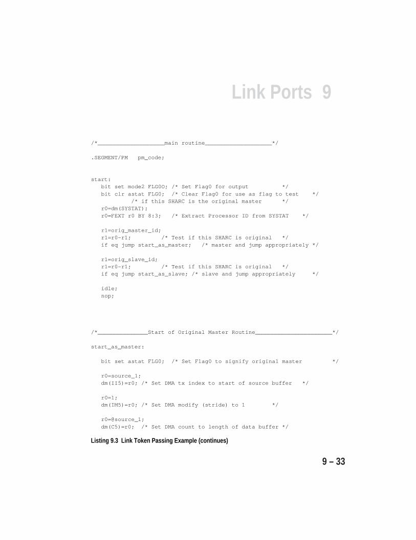
9Link Ports
9 – 33
Listing 9.3 Link Token Passing Example (continues)
/*____________________main routine____________________*/
.SEGMENT/PM pm_code;
start:bit set mode2 FLG0O; /* Set Flag0 for output */bit clr astat FLG0; /* Clear Flag0 for use as flag to test */
/* if this SHARC is the original master */r0=dm(SYSTAT);r0=FEXT r0 BY 8:3; /* Extract Processor ID from SYSTAT */
r1=orig_master_id;r1=r0-r1; /* Test if this SHARC is original */if eq jump start_as_master; /* master and jump appropriately */
r1=orig_slave_id;r1=r0-r1; /* Test if this SHARC is original */if eq jump start_as_slave; /* slave and jump appropriately */
idle;nop;
/*_______________Start of Original Master Routine_______________________*/
start_as_master:
bit set astat FLG0; /* Set Flag0 to signify original master */
r0=source_1;dm(II5)=r0; /* Set DMA tx index to start of source buffer */
r0=1;dm(IM5)=r0; /* Set DMA modify (stride) to 1 */
r0=@source_1;dm(C5)=r0; /* Set DMA count to length of data buffer */

9 Link Ports
9 – 34
r0=0xc000; /* LCOM Register: 2x rate on LBUF3, */dm(LCOM)=r0; /* note:use r0=0x00010000 on rev. 0.X silicon */
r0=0x3f1ff; /* LAR Register: LBUF3->port 0 */dm(LAR)=r0; /* All others inactive */
bit set imask LP3I; /* Enable Link buffer 3 interrupt */bit set mode1 IRPTEN; /* Global interrupt enable */
r0=0x0000b000; /* LCTL Register: 32-bit data, LBUF3=tx */dm(LCTL)=r0; /* enable DMA on LBUF3 */
/* This will start off the DMA transfer *//* Always write LCTL after LAR */
wait_1: idle; /* Wait for Link buffer 3 interrupt */ jump wait_1; /* Will end up here after entire DMA complete*/
nop; /* All master interrupts will come back to here */ nop;
/*__________________Link buffer 3 Interrupt Routine_____________________*/
lp3:if NOT FLAG0_IN jump lp3_orig_slave; /* Test for original master */nop; /* and jump appropriately */nop;
/*_______________Link buffer 3 Tx finish Interrupt Routine______________*/
lp3_orig_master:
Listing 9.3 Link Token Passing Example (continues)
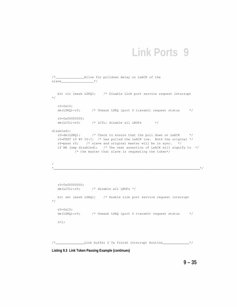
9Link Ports
9 – 35
/*_______________Allow for pulldown delay on LxACK of theslave_________________*/
bit clr imask LSRQI; /* Disable Link port service request interrupt*/
r0=0x10;dm(LSRQ)=r0; /* Unmask LSRQ lport 0 transmit request status */
r0=0x00000000;dm(LCTL)=r0; /* LCTL: disable all LBUFs */
disabled1:r0=dm(LSRQ); /* Check to ensure that the pull down on LxACK */r0=FEXT r0 BY 20:1; /* has pulled the LxACK low. Both the original */r0=pass r0; /* slave and original master will be in sync. */if NE jump disabled1; /* The next assertion of LxACK will signify to */
/* the master that slave is requesting the token*/
/*______________________________________________________________________________*/
r0=0x00000000;dm(LCTL)=r0; /* disable all LBUFs */
bit set imask LSRQI; /* Enable Link port service request interrupt*/
r0=0x10;dm(LSRQ)=r0; /* Unmask LSRQ lport 0 transmit request status */
rti;
/*_______________Link buffer 2 Tx finish Interrupt Routine______________*/
Listing 9.3 Link Token Passing Example (continues)
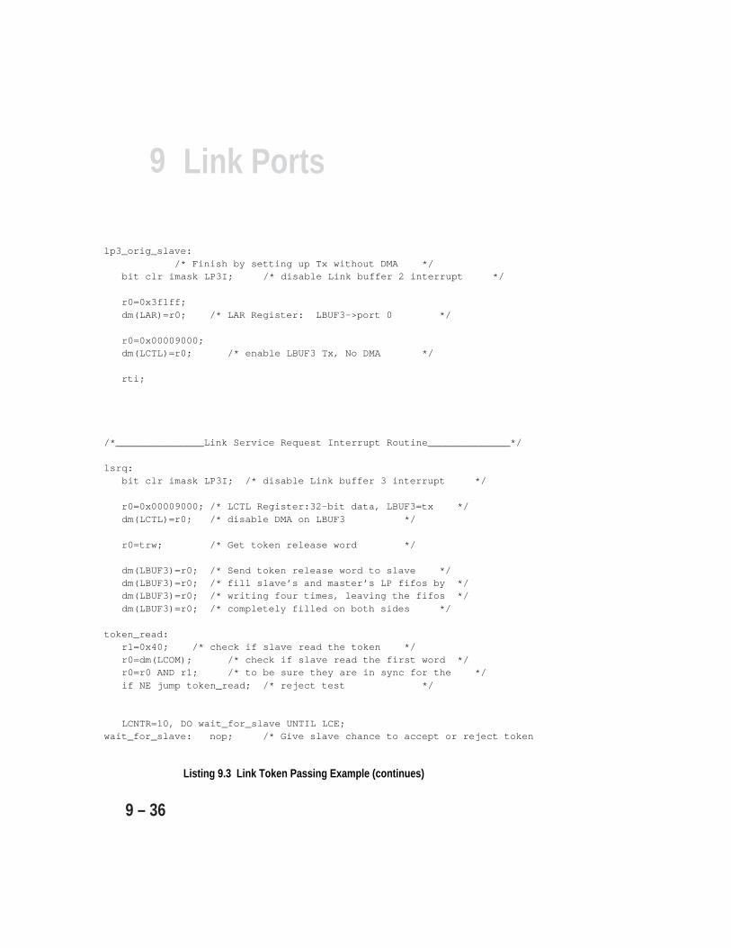
9 Link Ports
9 – 36
lp3_orig_slave:/* Finish by setting up Tx without DMA */
bit clr imask LP3I; /* disable Link buffer 2 interrupt */
r0=0x3f1ff;dm(LAR)=r0; /* LAR Register: LBUF3->port 0 */
r0=0x00009000;dm(LCTL)=r0; /* enable LBUF3 Tx, No DMA */
rti;
/*_______________Link Service Request Interrupt Routine______________*/
lsrq:bit clr imask LP3I; /* disable Link buffer 3 interrupt */
r0=0x00009000; /* LCTL Register:32-bit data, LBUF3=tx */dm(LCTL)=r0; /* disable DMA on LBUF3 */
r0=trw; /* Get token release word */
dm(LBUF3)=r0; /* Send token release word to slave */dm(LBUF3)=r0; /* fill slave’s and master’s LP fifos by */dm(LBUF3)=r0; /* writing four times, leaving the fifos */dm(LBUF3)=r0; /* completely filled on both sides */
token_read:r1=0x40; /* check if slave read the token */r0=dm(LCOM); /* check if slave read the first word */r0=r0 AND r1; /* to be sure they are in sync for the */if NE jump token_read; /* reject test */
LCNTR=10, DO wait_for_slave UNTIL LCE;wait_for_slave: nop; /* Give slave chance to accept or reject token
Listing 9.3 Link Token Passing Example (continues)
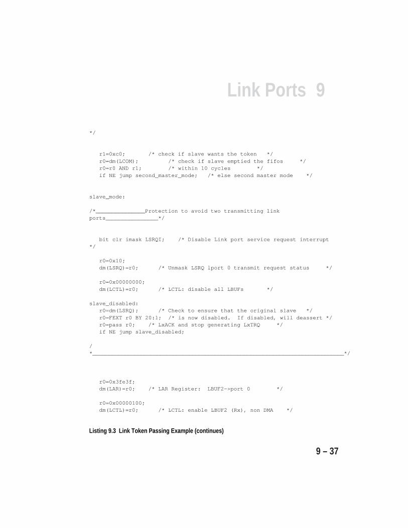
9Link Ports
9 – 37
*/
r1=0xc0; /* check if slave wants the token */r0=dm(LCOM); /* check if slave emptied the fifos */r0=r0 AND r1; /* within 10 cycles */if NE jump second_master_mode; /* else second master mode */
slave_mode:
/*_______________Protection to avoid two transmitting linkports________________*/
bit clr imask LSRQI; /* Disable Link port service request interrupt*/
r0=0x10;dm(LSRQ)=r0; /* Unmask LSRQ lport 0 transmit request status */
r0=0x00000000;dm(LCTL)=r0; /* LCTL: disable all LBUFs */
slave_disabled:r0=dm(LSRQ); /* Check to ensure that the original slave */r0=FEXT r0 BY 20:1; /* is now disabled. If disabled, will deassert */r0=pass r0; /* LxACK and stop generating LxTRQ */if NE jump slave_disabled;
/*______________________________________________________________________________*/
r0=0x3fe3f;dm(LAR)=r0; /* LAR Register: LBUF2->port 0 */
r0=0x00000100;dm(LCTL)=r0; /* LCTL: enable LBUF2 (Rx), non DMA */
Listing 9.3 Link Token Passing Example (continues)
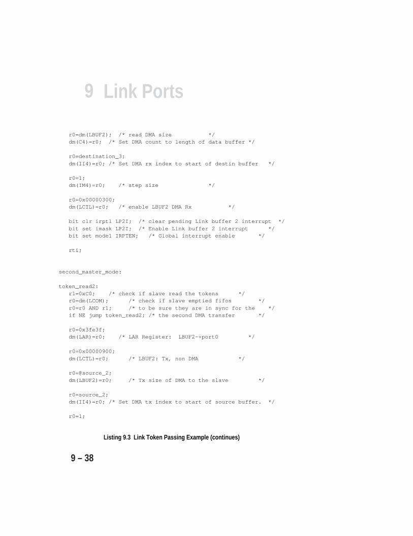
9 Link Ports
9 – 38
r0=dm(LBUF2); /* read DMA size */dm(C4)=r0; /* Set DMA count to length of data buffer */
r0=destination_3;dm(II4)=r0; /* Set DMA rx index to start of destin buffer */
r0=1;dm(IM4)=r0; /* step size */
r0=0x00000300;dm(LCTL)=r0; /* enable LBUF2 DMA Rx */
bit clr irptl LP2I; /* clear pending Link buffer 2 interrupt */bit set imask LP2I; /* Enable Link buffer 2 interrupt */bit set mode1 IRPTEN; /* Global interrupt enable */
rti;
second_master_mode:
token_read2:r1=0xC0; /* check if slave read the tokens */r0=dm(LCOM); /* check if slave emptied fifos */r0=r0 AND r1; /* to be sure they are in sync for the */if NE jump token_read2; /* the second DMA transfer */
r0=0x3fe3f;dm(LAR)=r0; /* LAR Register: LBUF2->port0 */
r0=0x00000900;dm(LCTL)=r0; /* LBUF2: Tx, non DMA */
r0=@source_2;dm(LBUF2)=r0; /* Tx size of DMA to the slave */
r0=source_2;dm(II4)=r0; /* Set DMA tx index to start of source buffer. */
r0=1;
Listing 9.3 Link Token Passing Example (continues)
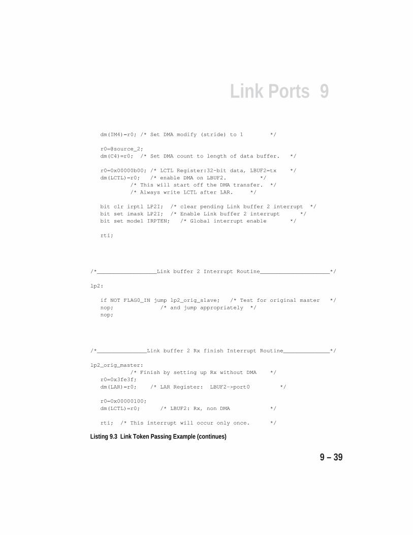
9Link Ports
9 – 39
dm(IM4)=r0; /* Set DMA modify (stride) to 1 */
r0=@source_2;dm(C4)=r0; /* Set DMA count to length of data buffer. */
r0=0x00000b00; /* LCTL Register:32-bit data, LBUF2=tx */dm(LCTL)=r0; /* enable DMA on LBUF2. */
/* This will start off the DMA transfer. *//* Always write LCTL after LAR. */
bit clr irptl LP2I; /* clear pending Link buffer 2 interrupt */bit set imask LP2I; /* Enable Link buffer 2 interrupt */bit set mode1 IRPTEN; /* Global interrupt enable */
rti;
/*__________________Link buffer 2 Interrupt Routine_____________________*/
lp2:
if NOT FLAG0_IN jump lp2_orig_slave; /* Test for original master */nop; /* and jump appropriately */nop;
/*_______________Link buffer 2 Rx finish Interrupt Routine______________*/
lp2_orig_master:/* Finish by setting up Rx without DMA */
r0=0x3fe3f;dm(LAR)=r0; /* LAR Register: LBUF2->port0 */
r0=0x00000100;dm(LCTL)=r0; /* LBUF2: Rx, non DMA */
rti; /* This interrupt will occur only once. */
Listing 9.3 Link Token Passing Example (continues)
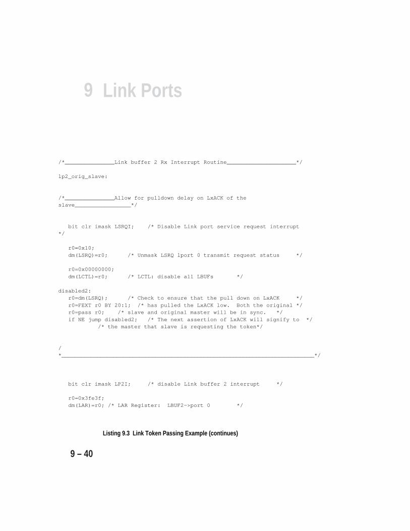
9 Link Ports
9 – 40
/*_______________Link buffer 2 Rx Interrupt Routine_____________________*/
lp2_orig_slave:
/*_______________Allow for pulldown delay on LxACK of theslave_________________*/
bit clr imask LSRQI; /* Disable Link port service request interrupt*/
r0=0x10;dm(LSRQ)=r0; /* Unmask LSRQ lport 0 transmit request status */
r0=0x00000000;dm(LCTL)=r0; /* LCTL: disable all LBUFs */
disabled2:r0=dm(LSRQ); /* Check to ensure that the pull down on LxACK */r0=FEXT r0 BY 20:1; /* has pulled the LxACK low. Both the original */r0=pass r0; /* slave and original master will be in sync. */if NE jump disabled2; /* The next assertion of LxACK will signify to */
/* the master that slave is requesting the token*/
/*______________________________________________________________________________*/
bit clr imask LP2I; /* disable Link buffer 2 interrupt */
r0=0x3fe3f;dm(LAR)=r0; /* LAR Register: LBUF2->port 0 */
Listing 9.3 Link Token Passing Example (continues)

9Link Ports
9 – 41
r0=0x00000100;dm(LCTL)=r0; /* LBUF2=rx (slave), No DMA */
bit clr mode1 NESTM; /* disable interrupt nesting *//* to avoid breaking sync */
r0=dm(LBUF2); /* read token permission from master */
/* The following check if the first word after DMA is token *//* permission. If it is not, the slave read other dummy words *//* and continue to be slave. If it is token permission, *//* continue the original flow and the slave will decide if *//* if will accept the permissiom. */
r1=trw; /* token release word */
r0 = r0 - r1; /* test received word and set ALU flag */if NE jump second_slave_mode; /* not token permission */nop;nop;
/* The following 3 lines shows how to reject token *//* If commented-out, this slave will change to master *//* if uncommented, this slave will continue to be slave */
/* LCNTR=20, DO reject_token UNTIL LCE;reject_token: nop;jump second_slave_mode;nop; /* delay read of incoming message */nop;
master_mode:
r0=dm(LBUF2); /* Read 3 times to clean the */r0=dm(LBUF2); /* ex-master’s LBUF. So, ex-master */r0=dm(LBUF2); /* will release the token */
Listing 9.3 Link Token Passing Example (continues)
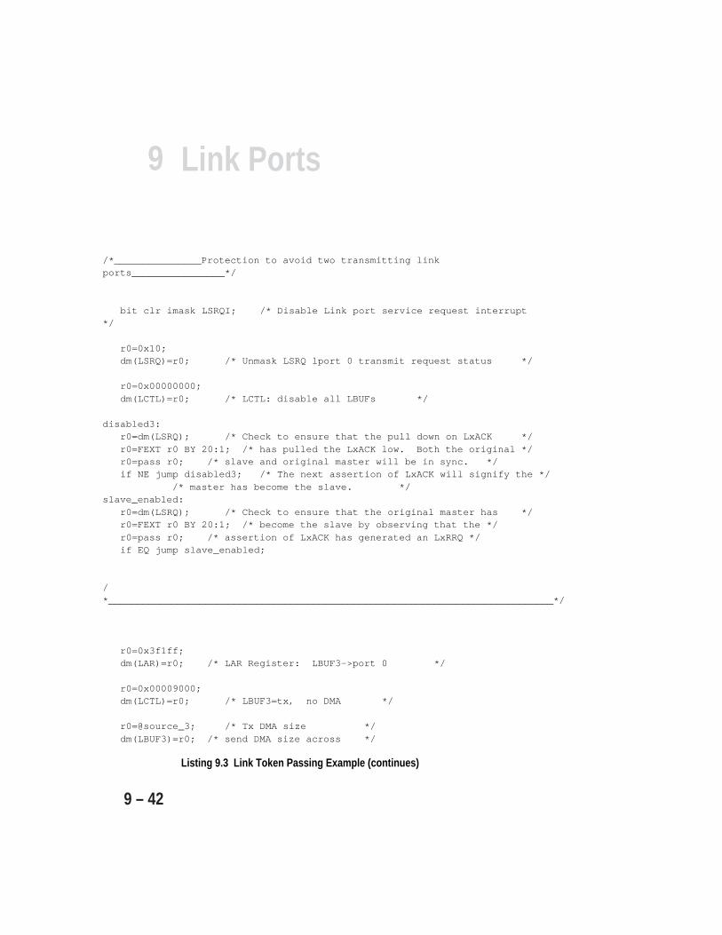
9 Link Ports
9 – 42
/*_______________Protection to avoid two transmitting linkports________________*/
bit clr imask LSRQI; /* Disable Link port service request interrupt*/
r0=0x10;dm(LSRQ)=r0; /* Unmask LSRQ lport 0 transmit request status */
r0=0x00000000;dm(LCTL)=r0; /* LCTL: disable all LBUFs */
disabled3:r0=dm(LSRQ); /* Check to ensure that the pull down on LxACK */r0=FEXT r0 BY 20:1; /* has pulled the LxACK low. Both the original */r0=pass r0; /* slave and original master will be in sync. */if NE jump disabled3; /* The next assertion of LxACK will signify the */
/* master has become the slave. */slave_enabled:
r0=dm(LSRQ); /* Check to ensure that the original master has */r0=FEXT r0 BY 20:1; /* become the slave by observing that the */r0=pass r0; /* assertion of LxACK has generated an LxRRQ */if EQ jump slave_enabled;
/*______________________________________________________________________________*/
r0=0x3f1ff;dm(LAR)=r0; /* LAR Register: LBUF3->port 0 */
r0=0x00009000;dm(LCTL)=r0; /* LBUF3=tx, no DMA */
r0=@source_3; /* Tx DMA size */dm(LBUF3)=r0; /* send DMA size across */
Listing 9.3 Link Token Passing Example (continues)
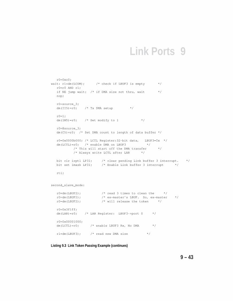
9Link Ports
9 – 43
r0=0xc0;wait: r1=dm(LCOM); /* check if LBUF3 is empty */
r0=r0 AND r1;if NE jump wait; /* if DMA size not thru, wait */nop;
r0=source_3;dm(II5)=r0; /* Tx DMA setup */
r0=1;dm(IM5)=r0; /* Set modify to 1 */
r0=@source_3;dm(C5)=r0; /* Set DMA count to length of data buffer */
r0=0x0000b000; /* LCTL Register:32-bit data, LBUF3=Tx */dm(LCTL)=r0; /* enable DMA on LBUF3 */
/* This will start off the DMA transfer *//* Always write LCTL after LAR */
bit clr irptl LP3I; /* clear pending Link buffer 3 interrupt. */bit set imask LP3I; /* Enable Link buffer 3 interrupt */
rti;
second_slave_mode:
r0=dm(LBUF2); /* read 3 times to clean the */r0=dm(LBUF2); /* ex-master’s LBUF. So, ex-master */r0=dm(LBUF2); /* will release the token */
r0=0x3f1ff;dm(LAR)=r0; /* LAR Register: LBUF3->port 0 */
r0=0x00001000;dm(LCTL)=r0; /* enable LBUF3 Rx, No DMA */
r1=dm(LBUF3); /* read new DMA size */
Listing 9.3 Link Token Passing Example (continues)
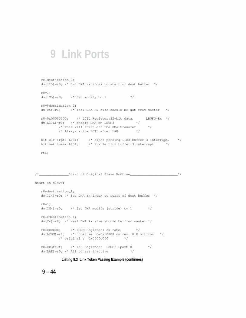
9 Link Ports
9 – 44
r0=destination_2;dm(II5)=r0; /* Set DMA rx index to start of dest buffer */
r0=1;dm(IM5)=r0; /* Set modify to 1 */
r0=@destination_2;dm(C5)=r1; /* real DMA Rx size should be got from master */
r0=0x00003000; /* LCTL Register:32-bit data, LBUF3=Rx */dm(LCTL)=r0; /* enable DMA on LBUF3 */
/* This will start off the DMA transfer *//* Always write LCTL after LAR */
bit clr irptl LP3I; /* clear pending Link buffer 3 interrupt. */bit set imask LP3I; /* Enable Link buffer 3 interrupt */
rti;
/*_______________Start of Original Slave Routine________________________*/
start_as_slave:
r0=destination_1;dm(II4)=r0; /* Set DMA rx index to start of dest buffer */
r0=1;dm(IM4)=r0; /* Set DMA modify (stride) to 1 */
r0=@destination_1;dm(C4)=r0; /* real DMA Rx size should be from master */
r0=0xc000; /* LCOM Register: 2x rate, */dm(LCOM)=r0; /* note:use r0=0x10000 on rev. 0.X silicon */
/* original : 0x0000c000 */
r0=0x3fe3f; /* LAR Register: LBUF2->port 0 */dm(LAR)=r0; /* All others inactive */
Listing 9.3 Link Token Passing Example (continues)
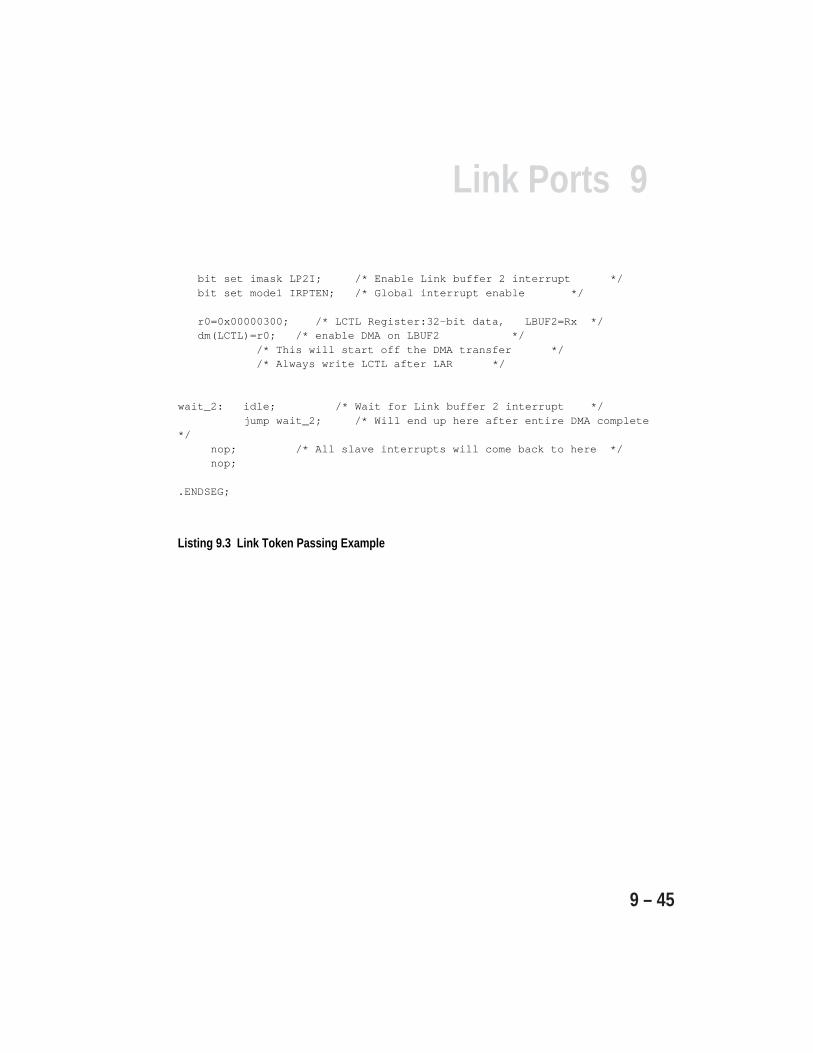
9Link Ports
9 – 45
bit set imask LP2I; /* Enable Link buffer 2 interrupt */bit set mode1 IRPTEN; /* Global interrupt enable */
r0=0x00000300; /* LCTL Register:32-bit data, LBUF2=Rx */dm(LCTL)=r0; /* enable DMA on LBUF2 */
/* This will start off the DMA transfer *//* Always write LCTL after LAR */
wait_2: idle; /* Wait for Link buffer 2 interrupt */ jump wait_2; /* Will end up here after entire DMA complete*/
nop; /* All slave interrupts will come back to here */ nop;
.ENDSEG;
Listing 9.3 Link Token Passing Example

9 Link Ports
9 – 46
10
10– 1
Serial Ports
10.1 OVERVIEWThe ADSP-2106x has two independent, synchronous serial ports,SPORT0 and SPORT1, that provide an I/O interface to a wide varietyof peripheral devices. Each serial port has its own set of controlregisters and data buffers. With a range of clock and framesynchronization options, the SPORTs allow a variety of serialcommunication protocols and provide a glueless hardware interface tomany industry-standard data converters and CODECs.
The serial ports can operate at the full clock rate of the processor,providing each with a maximum data rate of n Mbit/s, where n equalsthe processor clock frequency. Independent transmit and receivefunctions provide greater flexibility for serial communications. Serialport data can be automatically transferred to and from on-chipmemory using DMA block transfers. Each of the serial ports offers aTDM (time division multiplexed) multichannel mode.
Serial port clocks and frame syncs can be internally generated by theADSP-2106x or received from an external source. The serial ports canoperate with little-endian or big-endian transmission formats, withword lengths selectable from 3 to 32 bits. They offer selectablesynchronization and transmit modes as well as optional µ-law orA-law companding in hardware.
The serial ports offer the following features and capabilities:
• Independent transmit and receive functions.• Can transfer data words up to 32 bits in length, either MSB-first or LSB-first.• Double-buffering of data—both receive and transmit functions have a
data buffer register as well as a shift register; the double-bufferingprovides additional time to service the SPORT.
• A-law and µ-law hardware companding on transmitted and receivedwords.
• Serial clock and frame sync signals can be generated internally, in awide range of frequencies, or input from an external source.
• Interrupt-driven, single-word transfers to and from on-chip memorycontrolled by the ADSP-2106x core.
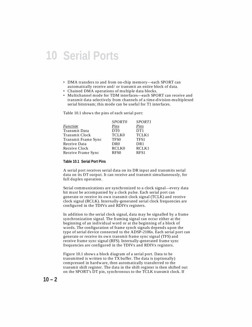
10 Serial Ports
10 – 2
• DMA transfers to and from on-chip memory—each SPORT canautomatically receive and/or transmit an entire block of data.
• Chained DMA operations of multiple data blocks.• Multichannel mode for TDM interfaces—each SPORT can receive and
transmit data selectively from channels of a time-division-multiplexedserial bitstream; this mode can be useful for T1 interfaces.
Table 10.1 shows the pins of each serial port:
SPORT0 SPORT1Function Pins PinsTransmit Data DT0 DT1Transmit Clock TCLK0 TCLK1Transmit Frame Sync TFS0 TFS1Receive Data DR0 DR1Receive Clock RCLK0 RCLK1Receive Frame Sync RFS0 RFS1
Table 10.1 Serial Port Pins
A serial port receives serial data on its DR input and transmits serialdata on its DT output. It can receive and transmit simultaneously, forfull duplex operation.
Serial communications are synchronized to a clock signal—every databit must be accompanied by a clock pulse. Each serial port cangenerate or receive its own transmit clock signal (TCLK) and receiveclock signal (RCLK). Internally-generated serial clock frequencies areconfigured in the TDIVx and RDIVx registers.
In addition to the serial clock signal, data may be signalled by a framesynchronization signal. The framing signal can occur either at thebeginning of an individual word or at the beginning of a block ofwords. The configuration of frame synch signals depends upon thetype of serial device connected to the ADSP-2106x. Each serial port cangenerate or receive its own transmit frame sync signal (TFS) andreceive frame sync signal (RFS). Internally-generated frame syncfrequencies are configured in the TDIVx and RDIVx registers.
Figure 10.1 shows a block diagram of a serial port. Data to betransmitted is written to the TX buffer. The data is (optionally)compressed in hardware, then automatically transferred to thetransmit shift register. The data in the shift register is then shifted outon the SPORT’s DT pin, synchronous to the TCLK transmit clock. If
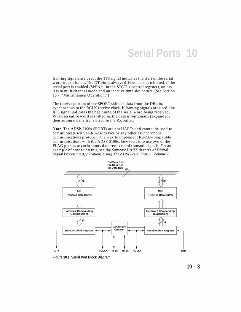
10Serial Ports
10 – 3
framing signals are used, the TFS signal indicates the start of the serialword transmission. The DT pin is always driven, i.e. not tristated, if theserial port is enabled (SPEN=1 in the STCTLx control register), unlessit is in multichannel mode and an inactive time slot occurs. (See Section10.7, “Multichannel Operation.”)
The receive portion of the SPORT shifts in data from the DR pin,synchronous to the RCLK receive clock. If framing signals are used, theRFS signal indicates the beginning of the serial word being received.When an entire word is shifted in, the data is (optionally) expanded,then automatically transferred to the RX buffer.
Note: The ADSP-2106x SPORTs are not UARTs and cannot be used tocommunicate with an RS-232 device or any other asynchronouscommunications protocol. One way to implement RS-232-compatiblecommunications with the ADSP-2106x, however, is to use two of theFLAG pins as asynchronous data receive and transmit signals. For anexample of how to do this, see the Software UART chapter of DigitalSignal Processing Applications Using The ADSP-2100 Family, Volume 2.
32
DM Data BusPM Data BusI/O Data Bus
32
TXn
Transmit Data Buffer
Hardware Companding(Compression)
Transmit Shift Register
32
32
RXn
Receive Data Buffer
Hardware Companding(Expansion)
Receive Shift Register
32
Serial PortControl
DRnRCLKnRFSnTCLKn TFSnDTn
Figure 10.1 Serial Port Block Diagram
10 Serial Ports
10 – 4
10.1.1 SPORT InterruptsEach serial port has a transmit DMA interrupt and a receive DMAinterrupt. When serial port DMA is not enabled, the interrupts occurfor each data word transmitted and received. The priority of the serialport interrupts is shown in Table 10.2.
InterruptName* InterruptSPR0I SPORT0 Receive DMA Channel Highest PrioritySPR1I SPORT1 Receive DMA ChannelSPT0I SPORT0 Transmit DMA ChannelSPT1I SPORT1 Transmit DMA Channel Lowest Priority
Table 10.2 SPORT Interrupts* These names are defined in the def21060.h include file supplied with theADSP-21000 Family Development Software.
SPORT Interrupts occur on the second system clock (CLKIN) after thelast bit of the serial word is latched in or driven out.
10.2 SPORT RESETRESETThere are two ways to reset the serial ports: a hardware reset using theRESET pin of the processor, and a software reset accomplished byclearing the serial port’s enable bit (SPEN) in the STCTLx and SRCTLxcontrol registers. Each method has a different effect on the serial port.
A hardware reset disables the serial ports by clearing the STCTLx andSRCTLx control registers (including the SPEN enable bits) and theTDIVx and RDIVx frame sync divisor registers. Any ongoingoperations are aborted.
A software reset of the SPEN enable bit(s) disables the serial port(s)and aborts any ongoing operations. Status bits are also cleared.
The serial ports will be ready to start transmitting or receiving datatwo CLKIN cycles after they are enabled (in the STCTLx or SRCTLxcontrol register). No serial clocks will be lost from this point on.

10Serial Ports
10 – 5
10.3 SPORT CONTROL REGISTERS & DATA BUFFERSThe registers used to control and configure the serial ports are part of theIOP register set. Each SPORT has its own set of the following controlregisters and data buffers:
RegisterName* FunctionSTCTLx SPORT Transmit Control RegisterTXx Transmit Data BufferTDIVx Transmit Clock & Frame Sync DivisorsMTCSx Multichannel Transmit SelectMTCCSx Multichannel Transmit Compand Select
SRCTLx SPORT Receive Control RegisterRXx Receive Data BufferRDIVx Receive Clock & Frame Sync DivisorsMRCSx Multichannel Receive SelectMRCCSx Multichannel Receive Compand Select
SPATHx SPORT Path Length (for mesh multiprocessing)
KEYWDx SPORT Receive Comparison**KEYMASKx SPORT Receive Comparison Mask** * x = 0, 1** ADSP-21061 only
Table 10.3 (on the next page) shows the memory-mapped address andreset initialization value of each SPORT register. All of the registers are 32bits wide, except for the 16-bit SPATHx register and location 0x00FF.(Note that for standard, non-mesh-multiprocessing operation of the serialports, the SPATHx register and location 0x00FF must remain equal to thereset initialization value, 0x0001.)
The SPORT control registers are programmed by writing to theappropriate address in memory. The symbolic names of the registers andindividual control bits can be used in ADSP-2106x programs—the#define definitions for these symbols are contained in the filedef21060.h which is provided in the INCLUDE directory of the ADSP-21000 Family Development Software. The def21060.h file is shown inthe Control/Status Registers appendix of this manual. All control and statusbits in the SPORT registers are active high unless otherwise noted.
Because the SPORT registers are memory-mapped they cannot be writtenwith data coming directly from memory. They must instead be written

10 Serial Ports
10 – 6
Memory Register InitializationAddress Name After RESET Description
0x00E0 STCTL0 0x0000 0000 SPORT0 Transmit Control Register0x00E1 SRCTL0 0x0000 0000 SPORT0 Receive Control Register0x00E2 TX0 ni SPORT0 Transmit Data Buffer0x00E3 RX0 ni SPORT0 Receive Data Buffer0x00E4 TDIV0 ni SPORT0 Transmit Divisor0x00E5 reserved0x00E6 RDIV0 ni SPORT0 Receive Divisor0x00E7 reserved0x00E8 MTCS0 ni SPORT0 Multichannel Transmit Select0x00E9 MRCS0 ni SPORT0 Multichannel Receive Select0x00EA MTCCS0 ni SPORT0 Multichannel Transmit Compand Select0x00EB MRCCS0 ni SPORT0 Multichannel Receive Compand Select0x00EC KEYWD ni SPORT0 Receive Comparison (ADSP-21061)0x00ED KEYMASK ni SPORT0 Receive Comparison Mask (ADSP-21061)0x00EE SPATH0 0x0001 SPORT0 Path Length (Mesh Multiprocessing)0x00EF 0x0001 reserved
0x00F0 STCTL1 0x0000 0000 SPORT1 Transmit Control Register0x00F1 SRCTL1 0x0000 0000 SPORT1 Receive Control Register0x00F2 TX1 ni SPORT1 Transmit Data Buffer0x00F3 RX1 ni SPORT1 Receive Data Buffer0x00F4 TDIV1 ni SPORT1 Transmit Divisor0x00F5 reserved0x00F6 RDIV1 ni SPORT1 Receive Divisor0x00F7 reserved0x00F8 MTCS1 ni SPORT1 Multichannel Transmit Select0x00F9 MRCS1 ni SPORT1 Multichannel Receive Select0x00FA MTCCS1 ni SPORT1 Multichannel Transmit Compand Select0x00FB MRCCS1 ni SPORT1 Multichannel Receive Compand Select0x00FC KEYWD ni SPORT1 Receive Comparison (ADSP-21061)0x00FD KEYMASK ni SPORT1 Receive Comparison Mask (ADSP-21061)0x00FE SPATH1 0x0001 SPORT1 Path Length (Mesh Multiprocessing)0x00FF 0x0001 reserved
ni= not initialized
Table 10.3 SPORT Register Addresses & Initialization
from (or read into) ADSP-2106x core registers, usually one of the general-purpose universal registers of the register file (R15–R0). The SPORTcontrol registers can also be written or read by external devices, i.e.another ADSP-2106x or a host processor, to set up a serial port DMAoperation, for example.
10.3.1 Register Writes & Effect LatencySPORT register writes are internally completed at the end of the sameCLKIN cycle in which they occur. The register will therefore read backthe newly written value on the very next cycle. When a read of one of theSTCTLx or SRCTLx control registers is immediately followed by a writeto that register, however, the write may take two cycles to complete.

10Serial Ports
10 – 7
After a write to a SPORT register, control and mode bit changesgenerally take effect in the second CLKIN cycle after the write iscompleted. The serial ports will be ready to start transmitting orreceiving two CLKIN cycles after they are enabled (in the STCTLx orSRCTLx control register). No serial clocks will be lost from this pointon.
10.3.2 Transmit & Receive Data Buffers (TX, RX)TX0 and TX1 are the transmit data buffers for SPORT0 and SPORT1.They are 32-bit buffers which must be loaded with the data to betransmitted; the data is loaded either by the DMA controller or by theprogram running on the ADSP-2106x core. RX0 and RX1 are thereceive data buffers for SPORT0 and SPORT1. They are 32-bit bufferswhich are automatically loaded from the receive shifter when acomplete word has been received. Word lengths of less than 32 bits areright-justified in the receive and transmit buffers.
The TX buffers act like a two-location FIFO because they have a dataregister plus an output shift register (see Figure 10.1); two 32-bit wordsmay be stored in TX at any one time. When the TX buffer is loaded andany previous word has been transmitted, the buffer contents areautomatically loaded into the output shifter. An interrupt is generatedwhen the output shifter has been loaded, signifying that the TX bufferis ready to accept the next word (i.e. the TX buffer is “not full”). Thisinterrupt will not occur if serial port DMA is enabled or if thecorresponding mask bit in the IMASK register is set.
The transmit underflow status bit (TUVF) will be set in the transmitcontrol register when a transmit frame synch occurs and no new datahas been loaded into TX. The TUVF status bit is “sticky” and is onlycleared by disabling the serial port.
The RX buffers act like a three-location FIFO because they have twodata registers plus an input shift register. Two complete 32-bit wordscan be stored in RX while a third word is being shifted in. The thirdword will overwrite the second if the first word has not been read out(by the ADSP-2106x core or the DMA controller). When this happens,the receive overflow status bit (ROVF) will be set in the receive controlregister. Almost three complete words can be received without the RXbuffer being read before overflow occurs. The overflow status isgenerated on the last bit of third word. The ROVF status bit is “sticky”and is only cleared by disabling the serial port.

10 Serial Ports
10 – 8
An interrupt is generated when the RX buffer has been loaded with areceived word (i.e. the RX buffer is “not empty”). This interrupt will bemasked out if serial port DMA is enabled or if the corresponding bit inthe IMASK register is set.
10.3.2.1 Reading & Writing RX, TXIf your ADSP-2106x program causes the core processor to attempt aread from an empty RX buffer or a write to a full TX buffer, the accessis delayed until the buffer is accessed by the external I/O device. (Thisdelay is called a core processor hang.) If it is not known whether thecore processor can access the RX or TX buffer without a hang, thebuffer’s full or empty status should be read first (in STCTLx or SRCTLx)to determine if the access can be made. To prevent this type of hangcondition from occurring, the BHD (Buffer Hang Disable) bit can be setin the SYSCON register.
The status bits in STCTLx and SRCTLx are updated during reads andwrites from the core processor even when the serial port is disabled.
The serial port should be disabled when writing to the RX buffer orreading from the TX buffer.
10.3.3 Transmit & Receive Control Registers (STCTL, SRCTL)The main control registers for each serial port are the transmit controlregister, STCTLx, and the receive control register, SRCTLx. Theseregisters are defined in Tables 10.4 and 10.5, and are pictured inFigures 10.2 and 10.3. When changing operating modes, a serial portcontrol register should be cleared (i.e. written with all zeros) before thenew mode is written to the register.
The Transmit Underflow Status bit (TUVF) is set whenever the TFSsignal occurs (from either external or internal source) while the TXbuffer is empty. The internally generated TFS may be suppressedwhenever TX is empty by clearing the DITFS control bit (DITFS=0).
When DITFS=0, the default, the transmit frame sync signal (TFS) isdependent upon new data being present in the TX buffer—the TFSsignal will only be generated for new data. Setting DITFS to 1 selectsdata-independent frame syncs. This causes the TFS signal to begenerated whether or not new data is present, transmitting thecontents of the TX buffer regardless. Serial port DMA will typicallykeep the TX buffer full, and when the DMA operation is complete thelast word in TX will be continuously transmitted.
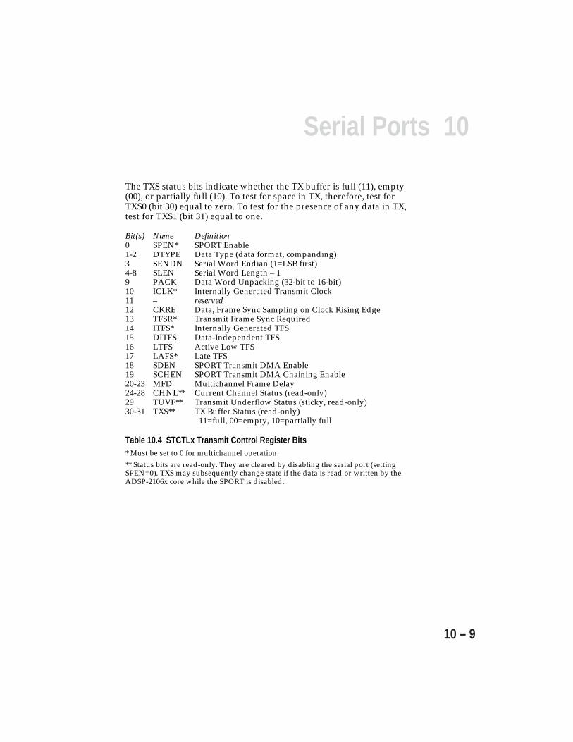
10Serial Ports
10 – 9
The TXS status bits indicate whether the TX buffer is full (11), empty(00), or partially full (10). To test for space in TX, therefore, test forTXS0 (bit 30) equal to zero. To test for the presence of any data in TX,test for TXS1 (bit 31) equal to one.
Bit(s) Name Definition0 SPEN* SPORT Enable1-2 DTYPE Data Type (data format, companding)3 SENDN Serial Word Endian (1=LSB first)4-8 SLEN Serial Word Length – 19 PACK Data Word Unpacking (32-bit to 16-bit)10 ICLK* Internally Generated Transmit Clock11 – reserved12 CKRE Data, Frame Sync Sampling on Clock Rising Edge13 TFSR* Transmit Frame Sync Required14 ITFS* Internally Generated TFS15 DITFS Data-Independent TFS16 LTFS Active Low TFS17 LAFS* Late TFS18 SDEN SPORT Transmit DMA Enable19 SCHEN SPORT Transmit DMA Chaining Enable20-23 MFD Multichannel Frame Delay24-28 CHNL** Current Channel Status (read-only)29 TUVF** Transmit Underflow Status (sticky, read-only)30-31 TXS** TX Buffer Status (read-only)
11=full, 00=empty, 10=partially full
Table 10.4 STCTLx Transmit Control Register Bits* Must be set to 0 for multichannel operation.
** Status bits are read-only. They are cleared by disabling the serial port (settingSPEN=0). TXS may subsequently change state if the data is read or written by theADSP-2106x core while the SPORT is disabled.
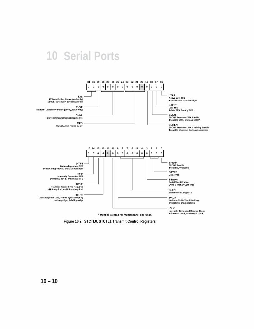
10 Serial Ports
10 – 10
MFDMultichannel Frame Delay
CHNLCurrent Channel Select (read-only)
26 25 24 23 22 21 20 19 18 17
000000000000
31 30 29 28 27
0000
16
LTFSActive Low TFS1=active low, 0=active high
LAFS*Late TFS1=late TFS, 0=early TFS
TUVFTransmit Underflow Status (sticky, read-only)
SDENSPORT Transmit DMA Enable1=enable DMA, 0=disable DMA
SCHENSPORT Transmit DMA Chaining Enable1=enable chaining, 0=disable chaining
TXSTX Data Buffer Status (read-only)
11=full, 00=empty, 10=partially full
11 10 9 8 7 6 5 4 3 2 1 0
00000000000
15 14 13 12
000
SPEN*SPORT Enable1=enable, 0=disable
DTYPEData Type
SENDNSerial Word Endian0=MSB-first, 1=LSB-first
SLENSerial Word Length – 1
PACK16-bit to 32-bit Word Packing1=packing, 0=no packing
DITFSData-Independent TFS
1=data-independent, 0=data-dependent
TFSR*Tranmsit Frame Sync Required
1=TFS required, 0=TFS not required
CKREClock Edge for Data, Frame Sync Sampling
1=rising edge, 0=falling edge
ICLKInternally Generated Receive Clock1=internal clock, 0=external clock
* Must be cleared for multichannel operation.
0 0
ITFS*Internally Generated TFS
1=internal TDFS, 0=external TFS
Figure 10.2 STCTL0, STCTL1 Transmit Control Registers
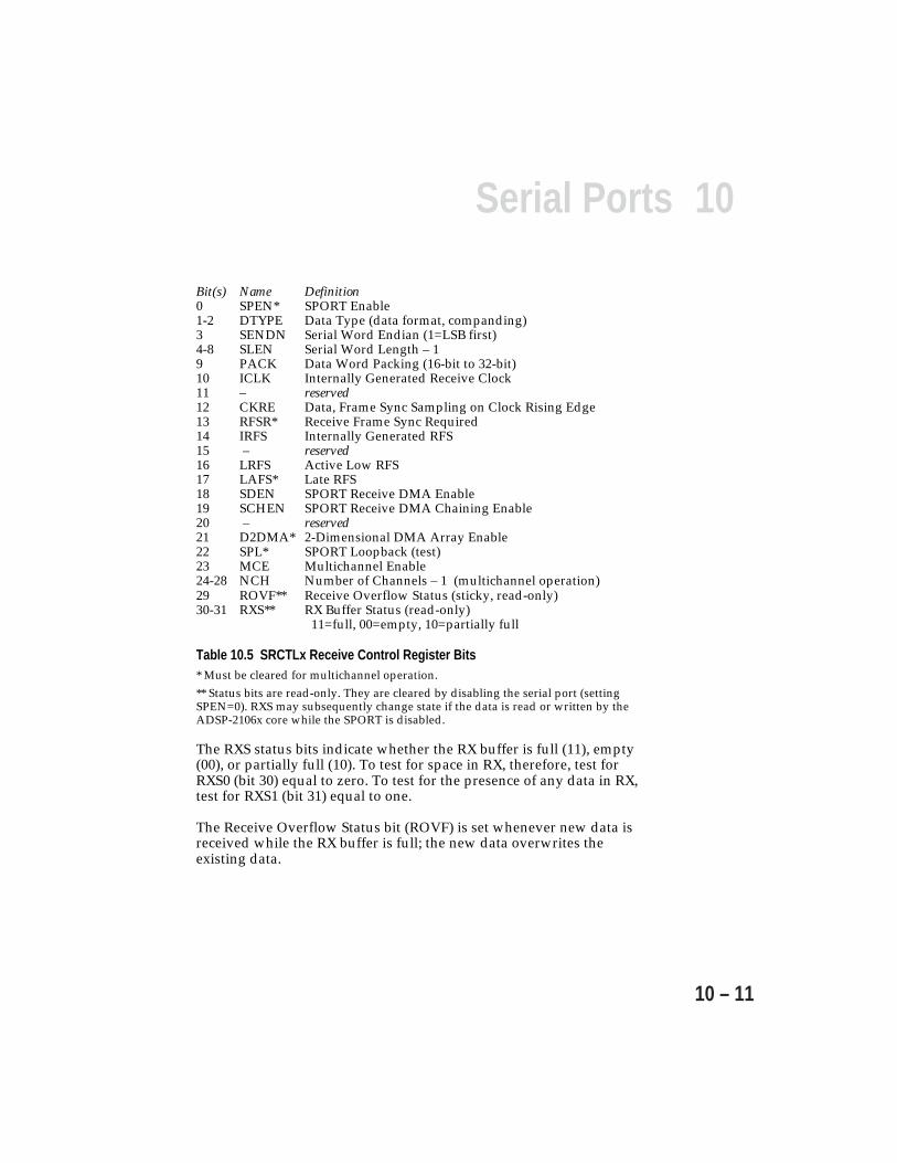
10Serial Ports
10 – 11
Bit(s) Name Definition0 SPEN* SPORT Enable1-2 DTYPE Data Type (data format, companding)3 SENDN Serial Word Endian (1=LSB first)4-8 SLEN Serial Word Length – 19 PACK Data Word Packing (16-bit to 32-bit)10 ICLK Internally Generated Receive Clock11 – reserved12 CKRE Data, Frame Sync Sampling on Clock Rising Edge13 RFSR* Receive Frame Sync Required14 IRFS Internally Generated RFS15 – reserved16 LRFS Active Low RFS17 LAFS* Late RFS18 SDEN SPORT Receive DMA Enable19 SCHEN SPORT Receive DMA Chaining Enable20 – reserved21 D2DMA* 2-Dimensional DMA Array Enable22 SPL* SPORT Loopback (test)23 MCE Multichannel Enable24-28 NCH Number of Channels – 1 (multichannel operation)29 ROVF** Receive Overflow Status (sticky, read-only)30-31 RXS** RX Buffer Status (read-only)
11=full, 00=empty, 10=partially full
Table 10.5 SRCTLx Receive Control Register Bits* Must be cleared for multichannel operation.** Status bits are read-only. They are cleared by disabling the serial port (settingSPEN=0). RXS may subsequently change state if the data is read or written by theADSP-2106x core while the SPORT is disabled.
The RXS status bits indicate whether the RX buffer is full (11), empty(00), or partially full (10). To test for space in RX, therefore, test forRXS0 (bit 30) equal to zero. To test for the presence of any data in RX,test for RXS1 (bit 31) equal to one.
The Receive Overflow Status bit (ROVF) is set whenever new data isreceived while the RX buffer is full; the new data overwrites theexisting data.
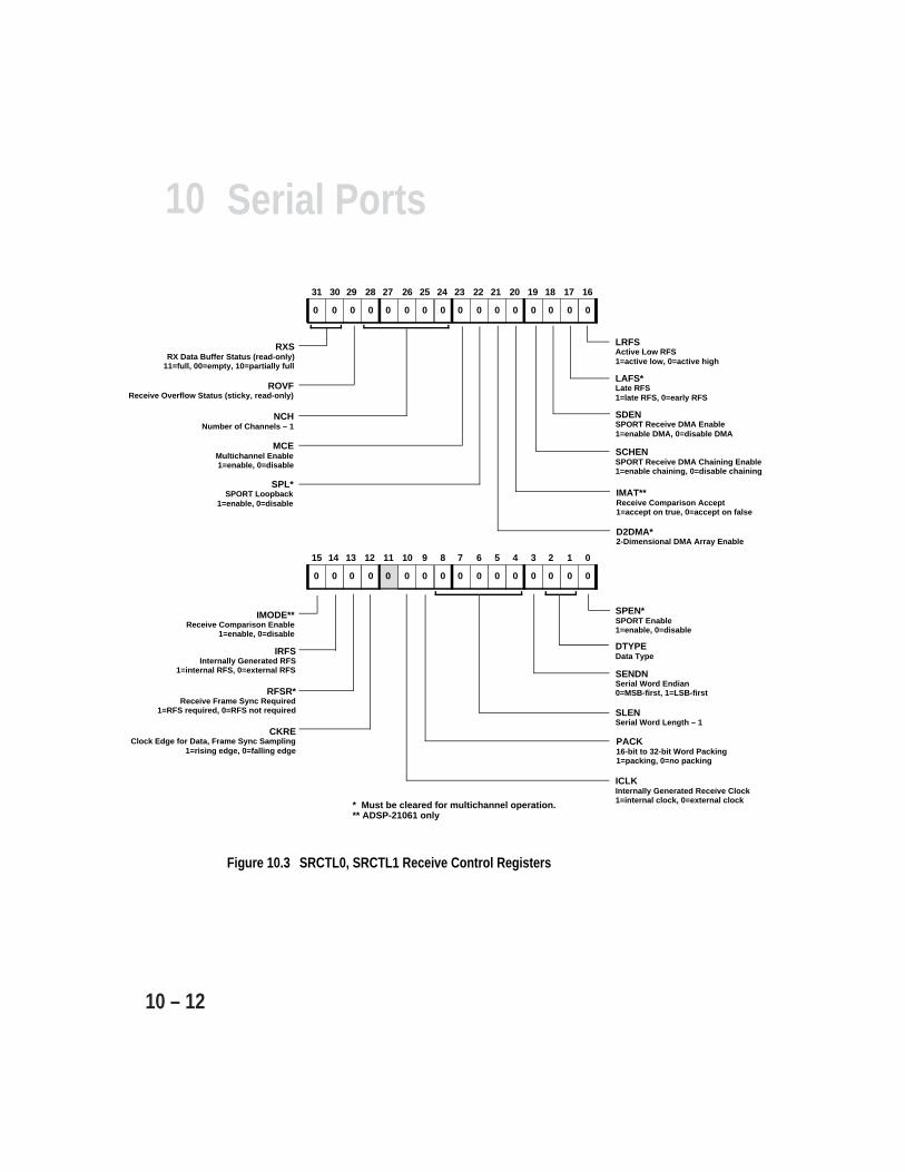
10 Serial Ports
10 – 12
MCEMultichannel Enable1=enable, 0=disable
NCHNumber of Channels – 1
SPL*SPORT Loopback
1=enable, 0=disableIMAT**Receive Comparison Accept1=accept on true, 0=accept on false
26 25 24 23 22 21 20 19 18 17
000000000000
31 30 29 28 27
0000
16
LRFSActive Low RFS1=active low, 0=active high
LAFS*Late RFS1=late RFS, 0=early RFS
ROVFReceive Overflow Status (sticky, read-only)
SDENSPORT Receive DMA Enable1=enable DMA, 0=disable DMA
SCHENSPORT Receive DMA Chaining Enable1=enable chaining, 0=disable chaining
RXSRX Data Buffer Status (read-only)
11=full, 00=empty, 10=partially full
11 10 9 8 7 6 5 4 3 2 1 0
00000000000
15 14 13 12
000
SPEN*SPORT Enable1=enable, 0=disable
DTYPEData Type
SENDNSerial Word Endian0=MSB-first, 1=LSB-first
SLENSerial Word Length – 1
PACK16-bit to 32-bit Word Packing1=packing, 0=no packing
IRFSInternally Generated RFS
1=internal RFS, 0=external RFS
RFSR*Receive Frame Sync Required
1=RFS required, 0=RFS not required
CKREClock Edge for Data, Frame Sync Sampling
1=rising edge, 0=falling edge
ICLKInternally Generated Receive Clock1=internal clock, 0=external clock* Must be cleared for multichannel operation.
** ADSP-21061 only
0 0
D2DMA*2-Dimensional DMA Array Enable
IMODE**Receive Comparison Enable
1=enable, 0=disable
Figure 10.3 SRCTL0, SRCTL1 Receive Control Registers

10Serial Ports
10 – 13
10.3.4 Clock & Frame Sync Frequencies (TDIV, RDIV)The TDIVx and RDIVx registers contain divisor values whichdetermine the frequencies for internally generated clocks and framesyncs. These registers are defined in Tables 10.6 and 10.7, and arepictured in Figures 10.4 and 10.5.
Bits Name Definition15-0 TCLKDIV Transmit Clock Divisor31-16 TFSDIV Transmit Frame Sync Divisor
Table 10.6 Transmit Divisor Register Bit Fields
Bits Name Definition15-0 RCLKDIV Receive Clock Divisor31-16 RFSDIV Receive Frame Sync Divisor
Table 10.7 Receive Divisor Register Bit Fields
Figure 10.4 TDIV0, TDIV1 Transmit Divisor Registers
11 10 9 8 7 6 5 4 3 2 1 015 14 13 12
26 25 24 23 22 21 20 19 18 1731 30 29 28 27 16
TCLKDIVTransmit Clock Divisor
TFSDIVTransmit Frame Sync Divisor

10 Serial Ports
10 – 14
11 10 9 8 7 6 5 4 3 2 1 015 14 13 12
26 25 24 23 22 21 20 19 18 1731 30 29 28 27 16
RCLKDIVReceive Clock Divisor
RFSDIVReceive Frame Sync Divisor
Figure 10.5 RDIV0, RDIV1 Receive Divisor Registers
TCLKDIV and RCLKDIV specify how many times the ADSP-2106xsystem clock (CLKIN) is divided to generate the transmit and receiveclocks. The divisor is a 16-bit value, allowing a wide range of serialclock rates. The following equation is used to calculate the serial clockfrequency:
fCLKINserial clock frequency = ———————
(xCLKDIV + 1)
The maximum serial clock frequency is equal to the ADSP-2106xsystem clock frequency, which occurs when xCLKDIV is set to zero.
Use the following equation to determine the value of xCLKDIV to use,given the CLKIN frequency and desired serial clock frequency:
fCLKINxCLKDIV = —————————— – 1
serial clock frequency
TFSDIV and RFSDIV specify how many transmit or receive clockcycles are counted before generating a TFS or RFS pulse (when theframe synch is internally generated). In this way a frame sync can beused to initiate periodic transfers. The counting of serial clock cyclesapplies to either internally or externally generated serial clocks.

10Serial Ports
10 – 15
The formula for the number of cycles between frame synch pulses is:
# of serial clock cycles between frame sync assertions = xFSDIV + 1
Use the following equation to determine the value of xFSDIV to use,given the serial clock frequency and desired frame sync frequency:
serial clock frequencyxFSDIV = —————————— – 1
frame sync frequency
The frame sync would thus be continuously active if xFSDIV=0.However, the value of xFSDIV should not be less than the serial wordlength minus one (the value of the SLEN field in the transmit orreceive control register), as this may cause an external device to abortthe current operation or cause other unpredictable results. If the serialport is not being used, the xFSDIV divisor can be used as a counter fordividing an external clock or for generating a periodic pulse orperiodic interrupt. The serial port must be enabled for this mode ofoperation to work.
10.3.4.1 Maximum Clock Rate RestrictionsCaution should be exercised when operating with externally generatedtransmit clocks near the frequency of the ADSP-2106x system clock.There is a delay between when the clock arrives at the TCLKx pin andwhen data is output—this delay may limit the receiver’s speed ofoperation. Refer to the data sheet for exact timing specifications. Forreliable operation, it is recommended that full-speed serial clocks onlybe used when receiving with an externally generated clock and externallygenerated frame sync (ICLK=0, IRFS=0).
Externally-generated late transmit frame syncs also experience a delayfrom when they arrive to when data is output—this can also limit themaximum serial clock speed. Refer to the data sheet for exact timingspecifications.
The serial ports handle word lengths of 3 to 32 bits, but transmitting orreceiving words smaller than 7 bits at the full clock rate of theADSP-2106x may cause incorrect operation when DMA chaining isenabled. Chaining disables the ADSP-2106x’s internal I/O bus forseveral cycles while the new TCB parameters are being loaded. Receivedata may be lost (i.e. overwritten) during this period.
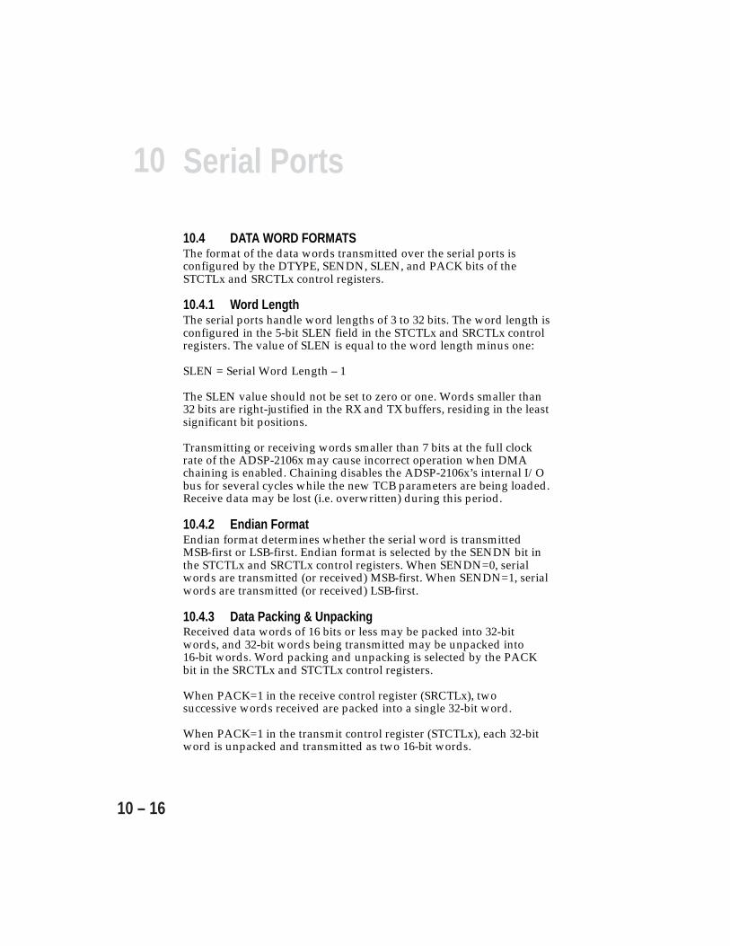
10 Serial Ports
10 – 16
10.4 DATA WORD FORMATSThe format of the data words transmitted over the serial ports isconfigured by the DTYPE, SENDN, SLEN, and PACK bits of theSTCTLx and SRCTLx control registers.
10.4.1 Word LengthThe serial ports handle word lengths of 3 to 32 bits. The word length isconfigured in the 5-bit SLEN field in the STCTLx and SRCTLx controlregisters. The value of SLEN is equal to the word length minus one:
SLEN = Serial Word Length – 1
The SLEN value should not be set to zero or one. Words smaller than32 bits are right-justified in the RX and TX buffers, residing in the leastsignificant bit positions.
Transmitting or receiving words smaller than 7 bits at the full clockrate of the ADSP-2106x may cause incorrect operation when DMAchaining is enabled. Chaining disables the ADSP-2106x’s internal I/Obus for several cycles while the new TCB parameters are being loaded.Receive data may be lost (i.e. overwritten) during this period.
10.4.2 Endian FormatEndian format determines whether the serial word is transmittedMSB-first or LSB-first. Endian format is selected by the SENDN bit inthe STCTLx and SRCTLx control registers. When SENDN=0, serialwords are transmitted (or received) MSB-first. When SENDN=1, serialwords are transmitted (or received) LSB-first.
10.4.3 Data Packing & UnpackingReceived data words of 16 bits or less may be packed into 32-bitwords, and 32-bit words being transmitted may be unpacked into16-bit words. Word packing and unpacking is selected by the PACKbit in the SRCTLx and STCTLx control registers.
When PACK=1 in the receive control register (SRCTLx), twosuccessive words received are packed into a single 32-bit word.
When PACK=1 in the transmit control register (STCTLx), each 32-bitword is unpacked and transmitted as two 16-bit words.
10Serial Ports
10 – 17
The first 16-bit (or smaller) word is right-justified in bits 15-0 of thepacked word, and the second 16-bit (or smaller) word is right-justifiedin bits 31-16. This applies for both receive (packing) and transmit(unpacking) operations. Companding may be used when wordpacking or unpacking is being used.
When serial port data packing is enabled, the transmit and receiveinterrupts are generated for the 32-bit packed words, not for each16-bit word.
Hint: When 16-bit received data is packed into 32-bit words and storedin normal word space in ADSP-2106x internal memory, the 16-bitwords can be read or written with short word space addresses.
10.4.4 Data TypeThe DTYPE field of the STCTLx and SRCTLx control registers specifiesone of four data formats (for non-multichannel operation):
DTYPE Data Formatting 00 Right-justify, zero-fill unused MSBs 01 Right-justify, sign-extend into unused MSBs 10 Compand using µ-law 11 Compand using A-law
These formats are applied to serial data words loaded into the RX andTX buffers. (TX data words are not actually zero-filled or sign-extended, since only the significant bits are transmitted.)
For multichannel operation, the companding selection and MSB-fillselection is independent:
DTYPE Data Formatting x0 Right-justify, zero-fill unused MSBs x1 Right-justify, sign-extend into unused MSBs 0x Compand using µ-law 1x Compand using A-law
Linear transfers will occur if the channel is active but companding isnot selected for that channel. Companded transfers will occur if thechannel is active and companding is selected for that channel. Themultichannel compand select registers, MTCCSx and MRCCSx, areused to specify which transmit and receive channels are companded.See “Channel Selection Registers” in the “Multichannel Operation”section of this chapter.
10 Serial Ports
10 – 18
Transmit sign extension is selected by bit 0 of DTYPE in the STCTLxregister and is common to all transmit channels. Receive sign extensionis selected by bit 0 of DTYPE in the SRCTLx register and is common toall receive channels. If bit 0 of DTYPE is set, sign extension will occuron selected channels that do not have companding selected. If this bitis not set, the word will contain 0s in the MSBs.
10.4.5 CompandingCompanding (compressing/expanding) is the process of logarithmicallyencoding and decoding data to minimize the number of bits that mustbe sent. The ADSP-2106x serial ports support the two most widelyused companding algorithms, A-law and µ-law, performed accordingto the CCITT G.711 specification. The type of companding can beselected independently for each SPORT. Companding is selected bythe DTYPE field of the STCTLx and SRCTLx control registers.
When companding is enabled, the data in the RX0 or RX1 buffer is theright-justified, sign-extended expanded value of the eight LSBsreceived. Likewise, a write to TX0 or TX1 causes the 32-bit value to becompressed to eight LSBs (sign-extended to the width of the transmitword) before it is transmitted. If the 32-bit value is greater than the13-bit A-law or 14-bit µ-law maximum, it is automatically compressedto the maximum value.
Because the values in the TX and RX buffers are actually compandedin-place, the companding hardware can be used without transmitting(or receiving) any data, for example during testing or debugging. Thisoperation requires a single cycle of overhead, as described below. Tocompand data in-place, without transmitting, the following sequenceof operations should be used:
1. Enable companding in the DTYPE field of the STCTLx transmitcontrol register.
2. Write a 32-bit data word to TX. (The companding is calculated in this cycle.)
3. Wait one cycle. A NOP instruction can be used to do this; if a NOP isnot inserted, the ADSP-2106x core will be held off for one cycleanyway. (This allows the serial port companding hardware to reload TXwith the companded value.)
4. Read the 8-bit companded value from TX.
10Serial Ports
10 – 19
To expand data in-place, the same sequence of operations is used butwith RX rather than TX. When expanding data in this way, be sure thatthe serial word length (SLEN) is set appropriately in the SRCTLxcontrol register.
With companding enabled, interfacing the ADSP-2106x serial port to acodec requires little additional programming effort. If companding isnot selected, there are two formats available for received data words offewer than 32 bits: one that fills unused MSBs with zeros, and anotherthat sign-extends the MSB into the unused bits (see the previoussection, “Data Type”).
10.5 CLOCK SIGNAL OPTIONSEach serial port has a transmit clock signal (TCLKx) and a receive clocksignal (RCLKx). The clock signals are configured by the ICLK andCKRE bits of the STCTLx and SRCTLx control registers. Serial clockfrequency is configured in the TDIVx and RDIVx registers.
The receive clock pin may be tied to the transmit clock if a single clockis desired for both input and output.
10.5.1 Internal vs. External ClocksBoth transmit and receive clocks can be independently generatedinternally or input from an external source. The ICLK bit of theSTCTLx and SRCTLx control registers determines the clock source.
When ICLK=1, the clock signal is generated internally by theADSP-2106x and the TCLKx or RCLKx pins will be an output. Theclock frequency is determined by the value of the serial clock divisor(TCLKDIV or RCLKDIV) in the TDIVx or RDIVx registers.
When ICLK=0, the clock signal is accepted as an input on the TCLKxor RCLKx pins, and the serial clock divisors in the TDIVx/RDIVxregisters are ignored. The externally generated serial clock need not besynchronous with the ADSP-2106x system clock.

10 Serial Ports
10 – 20
10.6 FRAME SYNC OPTIONSFraming signals indicate the beginning of each serial word transfer.The framing signals for each serial port are TFS (transmit framesynchronization) and RFS (receive frame synchronization). A variety offraming options are available; these options are configured in the serialport control registers. The TFS and RFS signals of a serial port areindependent and are separately configured in the control registers.
10.6.1 Framed vs. UnframedThe use of frame sync signals is optional in serial portcommunications. The TFSR (transmit frame sync required) and RFSR(receive frame sync required) control bits determine whether framesync signals are required. These bits are located in the the STCTLx andSRCTLx control registers.
When TFSR=1 or RFSR=1, a frame sync signal is required for everydata word. To allow continuous transmitting from the ADSP-2106x,each new data word must be loaded into the TX buffer before theprevious word is shifted out and transmitted. (See “Data-IndependentFrame Syncs” in this chapter.)
When TFSR=0 or RFSR=0, the corresponding frame sync signal is notrequired. A single frame sync is needed to initiate communications butis ignored after the first bit is transferred. Data words are thentransferred continuously, unframed. (Caution: When DMA is enabledin this mode, with frame syncs not required, DMA requests may beheld off by chaining or may not be serviced frequently enough toguarantee continuous unframed data flow.)
Figure 10.6 illustrates framed serial transfers, which have the followingcharacteristics:
• TFSR and RFSR bits in STCTLx, SRCTLx control registersdetermine framed or unframed mode.
• Framed mode requires a framing signal for every word. Unframedmode ignores framing signal after first word.
• Unframed mode is appropriate for continuous reception.• Active-low or active-high frame syncs selected with LTFS and LRFS
bits of STCTLx, SRCTLx control registers.
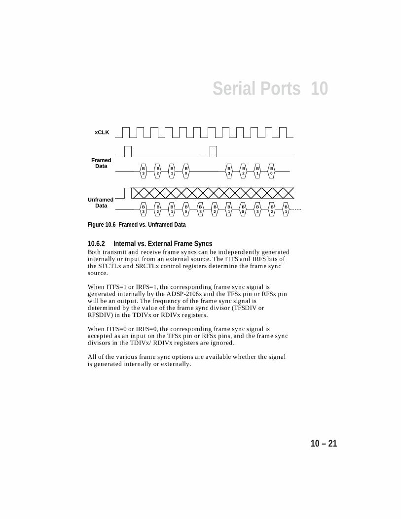
10Serial Ports
10 – 21
B3
B2
B1
B0
B3
B2
B1
B0
B3
B2
B1
B0
B3
B2
B1
B0
B3
B2
B1
xCLK
FramedData
UnframedData
Figure 10.6 Framed vs. Unframed Data
10.6.2 Internal vs. External Frame SyncsBoth transmit and receive frame syncs can be independently generatedinternally or input from an external source. The ITFS and IRFS bits ofthe STCTLx and SRCTLx control registers determine the frame syncsource.
When ITFS=1 or IRFS=1, the corresponding frame sync signal isgenerated internally by the ADSP-2106x and the TFSx pin or RFSx pinwill be an output. The frequency of the frame sync signal isdetermined by the value of the frame sync divisor (TFSDIV orRFSDIV) in the TDIVx or RDIVx registers.
When ITFS=0 or IRFS=0, the corresponding frame sync signal isaccepted as an input on the TFSx pin or RFSx pins, and the frame syncdivisors in the TDIVx/RDIVx registers are ignored.
All of the various frame sync options are available whether the signalis generated internally or externally.
10 Serial Ports
10 – 22
10.6.3 Active Low vs. Active High Frame SyncsFrame sync signals may be either active high or active low (i.e.inverted). The LTFS and LRFS bits of the STCTLx and SRCTLx controlregisters determine the frame syncs’ logic level.
When LTFS=0 or LRFS=0, the corresponding frame sync signal will beactive high.
When LTFS=1 or LRFS=1, the corresponding frame sync signal will beactive low.
Active high frame syncs are the default; the LTFS and LRFS bits areinitialized to 0 after a processor reset.
10.6.4 Sampling Edge For Data & Frame SyncsData and frame syncs can be sampled on either the rising or fallingedges of the serial port clock signals. The CKRE bit of the STCTLx andSRCTLx control registers selects the sampling edge.
For transmit data and frame syncs, setting CKRE=1 in STCTLx selectsthe rising edge of TCLKx. CKRE=0 selects the falling edge. Note thatdata and frame sync signals will change state on the clock edge that isnot selected.
For receive data and frame syncs, setting CKRE=1 in SRCTLx selectsthe rising edge of RCLKx. CKRE=0 selects the falling edge.
The transmit and receive functions of two serial ports connectedtogether, for example, should always select the same value for CKREso that any internally generated signals are driven on one edge andany received signals are sampled on the opposite edge.
10Serial Ports
10 – 23
10.6.5 Early vs. Late Frame SyncsFrame sync signals can occur during the first bit of each data word(“late”) or during the serial clock cycle immediately preceding the firstbit (“early”). The LAFS bit of the STCTLx and SRCTLx control registersconfigures this option.
When LAFS=0, early frame syncs are configured; this is the normalmode of operation. In this mode, the first bit of the transmit data wordis available (and the first bit of the receive data word is latched) in theserial clock cycle after the frame sync is asserted, and the frame sync isnot checked again until the entire word has been transmitted (orreceived). (In multichannel operation, this is the case when framedelay is 1.)
If data transmission is continuous in early framing mode (i.e. the lastbit of each word is immediately followed by the first bit of the nextword), then the frame sync signal occurs during the last bit of eachword. Internally generated frame syncs are asserted for one clock cyclein early framing mode.
When LAFS=1, late frame syncs are configured; this is the alternatemode of operation. In this mode, the first bit of the transmit data wordis available (and the first bit of the receive data word is latched) in thesame serial clock cycle that the frame sync is asserted. (In multichanneloperation, this is the case when frame delay is zero.) Receive data bitsare latched by serial clock edges, but the frame sync signal is onlychecked during the first bit of each word. Internally generated framesyncs remain asserted for the entire length of the data word in lateframing mode. Externally generated frame syncs are only checkedduring the first bit.

10 Serial Ports
10 – 24
B3 B2 B1 B0 ...
xCLK
LateFrameSync
Data
EarlyFrameSync
Figure 10.7 Normal vs. Alternate Framing
Figure 10.7 illustrates the two modes of frame signal timing:
• LAFS bits of STCTLx, SRCTLx control registers. LAFS=0 for earlyframe syncs, LAFS=1 for late frame syncs.
• Early framing: frame sync precedes data by one cycle. Late framing:frame sync checked on first bit only.
• Data transmitted MSB-first (SENDN=0) or LSB-first (SENDN=1).• Frame sync and clock generated internally or externally.
10.6.6 Data-Independent Transmit Frame SyncNormally the internally generated transmit frame sync signal (TFS) isoutput only when the TX buffer has data ready to transmit. The DITFSmode (data-independent transmit frame sync) allows the continuousgeneration of the TFS signal, with or without new data. The DITFS bitof the STCTLx control register configures this option.
When DITFS=0, the internally generated TFS is only output when anew data word has been loaded into the TX buffer. Once data is loadedinto TX, it is not transmitted until the next TFS is generated. This modeof operation allows data to be transmitted only at specific times.
10Serial Ports
10 – 25
When DITFS=1, the internally generated TFS is output at itsprogrammed interval regardless of whether new data is available inthe TX buffer. Whatever data is present in TX will be retransmittedwith each assertion of TFS. The TUVF transmit underflow status bit(in the STCTLx control register) will be set when this occurs (i.e. whenold data is retransmitted). The TUVF status bit is also set if the TXbuffer does not have new data when an externally generated TFSoccurs. Note that in this mode of operation, the first internallygenerated TFS will be delayed until data has been loaded into the TXbuffer.
If the internally generated TFS is used, a single write to the TX dataregister is required to start the transfer.
10.7 MULTICHANNEL OPERATIONThe ADSP-2106x serial ports offer a multichannel mode of operationwhich allows the SPORT to communicate in a time-division-multiplexed (TDM) serial system. In multichannel communications,each data word of the serial bit stream occupies a separate channel—each word belongs to the next consecutive channel so that, forexample, a 24-word block of data contains one word for each of 24channels.
The serial port can automatically select words for particular channelswhile ignoring the others. Up to 32 channels are available fortransmitting or receiving—each SPORT can receive and transmit dataselectively from any of the 32 channels. In other words, the SPORT cando any of the following on each channel:
1. transmit data,2. receive data,3. transmit and receive data, or4. do nothing
Data companding and DMA transfers can also be used in multichannelmode.
The DT pin is always driven, i.e. not tristated, if the serial port isenabled (SPEN=1 in the STCTLx control register), unless it is inmultichannel mode and an inactive time slot occurs.
Note that (in multichannel mode) the TCLKx pin is always an inputand must be connected to its corresponding RCLKx pin.
10 Serial Ports
10 – 26
Figure 10.8 shows example timing for a multichannel transfer, whichhave the following characteristics:
• Uses TDM method where serial data is sent or received on differentchannels sharing the same serial bus.
• The number of channels is selected with the NCH bits of SRCTLx:NCH=(# of channels) – 1.
• Can independently select transmit and receive channels.• RFS signal start of frame.• TFS is used as “Transmit Data Valid” for external logic; active only
during transmit channels.• Example: Receive on channels 0 and 2.
Transmit on channels 1 and 2.
SCLK
B3 B2 B1 B2DR
RFS
B0 IGNORED B3
DT B2B3 B0 B3 B2B1
WORD 0 WORD 1 WORD 2
TFS
Figure 10.8 Multichannel Operation
10.7.1 Frame Syncs In Multichannel ModeAll receiving and transmitting devices in a multichannel system musthave the same timing reference. The RFS signal is used for thisreference, indicating the start of a block (or frame) of multichanneldata words.
When multichannel mode is enabled on a SPORT, both the transmitterand receiver use RFS as a frame sync. This is true whether RFS isgenerated internally or externally. The RFS signal is used tosynchronize the channels and restart each multichannel sequence. RFSassertion occurs the beginning of the channel 0 data word.
TFS is used as a transmit data valid signal which is active duringtransmission of an enabled word. Since the serial port’s DTx pin istristated when the time slot is not active, the TFS signal specifies
10Serial Ports
10 – 27
whether or not DTx is being driven by the ADSP-2106x. The ADSP-2106x drives TFS in multichannel mode whether or not ITFS is cleared.After the TX transmit buffer is loaded, transmission begins and the TFSsignal is generated. When serial port DMA is being used, this mayhappen several cycles after the multichannel transmission is enabled. Ifa deterministic start time is required, the TX buffer should bepreloaded.
Note: TFS is normally left unconnected in multichannel mode, and theRFS pins of the serial port(s) are usually connected together.
10.7.2 Multichannel Control Bits In STCTL, SRCTLThe STCTLx and SRCTLx control registers contain several bits used toenable and configure multichannel operations.
10.7.2.1 Multichannel EnableMultichannel mode is enabled by setting the MCE bit in the SRCTLxcontrol register.
When MCE=1, multichannel operation is enabled.
When MCE=0, all multichannel operations are disabled.
Multichannel operation is activated three cycles after MCE is set.Internally generated frame sync signals activate four cycles after MCEis set.
Setting the MCE bit enables multichannel operation for both receiveand transmit sides of the SPORT. A transmitting SPORT must thereforebe in multichannel mode if the receiving SPORT is in multichannelmode.
10.7.2.2 Number Of ChannelsThe number of channels used in multichannel operation is selected bythe 5-bit NCH field in the SRCTLx control register. NCH should be setto the actual number of channels minus one:
NCH = Number of Channels – 1
10.7.2.3 Current Channel IndicatorThe 5-bit CHNL field in the STCTLx control register indicates whichchannel is currently selected during multichannel operation. This fieldis a read-only status indicator. CHNL(4:0) increments moduloNCH(4:0) as each channel is serviced.
10 Serial Ports
10 – 28
10.7.2.4 Multichannel Frame DelayThe 4-bit MFD field in the STCTLx control register specifies a delay betweenthe frame sync pulse and the first data bit in multichannel mode. The valueof MFD is the number of serial clock cycles of the delay. Multichannel framedelay allows the processor to work with different types of T1 interfacedevices.
A value of zero for MFD causes the frame sync to be concurrent with thefirst data bit. The maximum value allowed for MFD is 15. A new frame syncmay occur before data from the last frame has been received, because blocksof data occur back to back.
A multichannel frame delay of at least one should be used when theADSP-2106x is generating frame syncs for the multichannel system and theserial clock of the system is equal to CLKIN (the processor clock). If MFD isnot set to at least one, the master ADSP-2106x in a multiprocessing systemwill not recognize the first frame sync after multichannel operation isenabled. All succeeding frame syncs will be recognized normally, however.
10.7.3 Channel Selection RegistersSpecific channels can be individually enabled or disabled to select whichwords are received and transmitted during multichannel communications.Data words from the enabled channels are received or transmitted, whiledisabled channel words are ignored. Up to 32 channels are available fortransmitting and up to 32 channels for receiving.
The multichannel selection registers are used to enable and disableindividual channels. The registers for each serial port are as follows:
RegisterName FunctionMTCSx Multichannel Transmit Select—specifies the active transmit channelsMRCSx Multichannel Receive Select—specifies the active receive channelsMTCCSx Multichannel Transmit Compand Select—specifies which active
transmit channels are compandedMRCCSx Multichannel Receive Compand Select—specifies which active receive
channels are companded
Each register has 32 bits, corresponding the 32 channels. Setting a bitenables that channel so that the serial port will select its word from themultiple-word block of data (for either receive or transmit). For example,setting bit 0 selects word 0, setting bit 12 selects word 12, and so on.

10Serial Ports
10 – 29
Setting a particular bit to 1 in the MTCSx register causes the serial port totransmit the word in that channel’s position of the data stream. Clearingthe bit to 0 in the MTCSx register causes the serial port’s DT (datatransmit) pin to tristate during the time slot of that channel.
Setting a particular bit to 1 in the MRCSx register causes the serial port toreceive the word in that channel’s position of the data stream; the receivedword is loaded into the RX buffer. Clearing the bit to 0 in the MRCSxregister causes the serial port to ignore the data.
Companding may be selected on a per-channel basis. The MTCCSx andMRCCSx registers are used to specify companding for any activechannels. Setting a bit to 1 in these registers causes the data to becompanded. A-law or µ-law companding is selected with the DTYPE bit 1in the STCTLx and SRCTLx control registers.
10.7.4 SPORT Receive Comparison RegistersOn the ADSP-21061, two sets of registers aid multiprocessorcommunications when using multichannel mode (MCE=1) through theserial ports. These 32-bit registers are the Receive Comparison (KEYWDx)registers and the Receive Comparison Mask (KEYMASKx) registers.
The KEYWD0 or KEYWD1 register stores the pattern to be matched withthe incoming data. The corresponding KEYMASK0 or KEYMASK1register specifies which of the bits in the received data should becompared. Setting a KEYMASKx bit (=1) masks the corresponding bit inthe KEYWDx register, disabling its comparison.
The processor receiving the data compares it with the data in theKEYWDx register. Depending on the comparison results, the receiveddata is accepted or ignored. If accepted, the receiver requests—based onthe setting to the SRCTL register—a DMA transfer to internal memory orgenerates an interrupt.
In addition to the MCE setting, the following bits in the SRCTL registercontrol the operation of Receive Comparison:
IMODE IMAT(Bit 15) (Bit 20) Operation
0 x Receive comparison disabled1 0 Accept receive data if the KEYWD comparison is false1 1 Accept receive data if the KEYWD comparison is true
10 Serial Ports
10 – 30
When receive comparison is enabled, companding is disabled on thetransmitter and receiver. The MTCCSx register, which selectsmultichannel companding when receive comparison is disabled,determines whether the DSP performs a KEYWD comparison for theenabled received channels. If the MTCCSx bit for a particlular channelis '0,' the processor does not perform a comparison and always acceptsthe receive data on that channel. If the MTCCSx bit for a particularchannel is '1,' the processor performs the comparison and accepts (orrejects) the receive data, depending on the result of the comparisonand IMAT setting in the SRCTLx register.
The receive comparison feature lets the ADSP-21061's SPORTSgenerate a DMA request or an interrupt when the received datamatches a specified condition on a specified channel in multichannelmode. Without this feature, the SPORT would interrupt the processorevery time data was received and the processor would be required tocheck if the data was meant for it or not. It is possible that most of thetime the data being sent is not meant for the processor. With thereceive comparison feature, the SPORT on a particular processor canbe programmed to interrupt only on messages meant for thatprocessor.
As a receive comparison example, consider four ADSP-21061s (A, B, C,and D) which use SPORT0 (in multichannel mode) for interprocessorcommunication. Channels 0, 1, 2, and 3 are used respectively by A, B,C, and D to transmit control information between the processors.Channels 4 through 10, 11 through 17, 18 through 24, and 25 through31 are used respectively by A, B, C, and D to transmit data.
Because channels 0 through 3 are used to send control informationbetween the processors, the comparisons for incoming data is enabledonly for these channels. Initially, channels 4 through 31 may havereceive disabled. For this example, consider communication betweenprocessors A and B only. The key word for comparison isprogrammable; in this example, processor B can check for the keyword "START TRANSMIT TO B",
10Serial Ports
10 – 31
Processor B can check for this key word as follows:
1. Set the KEYWD register to "START TRANSMIT TO B"
2. Clear bits 31:16 of the KEYMASK register to 0 and set the otherbits to 1This step enables comparison only for bits 31:16. So, assume thatthe code for "START TRANSMIT TO B" only uses bits 31:16 andbits 15:0 indicate the source of the transmission and the datachannels.
3. Set bits 15 and 20 of the SRCTL register to 1This step enables the SPORT to generate an interrupt or DMArequest only if the incoming data matches the KEYWD.
4. Set bits 0 through 3 of the Transmit Compand Channel Selectorregister to 1 and clear the remaining bits to 0This step enables comparison only on channels 0 through 3.
Until it receives the "START TRANSMIT TO B" keyword, processor Bignores all transmissions that it receives. When processor A wants tosend data to B, it sends the "START TRANSMIT TO B" keyword onchannel 0. When receive comparison on processor B recognizes the"START TRANSMIT TO B" keyword, the SPORT interrupts processorB. Then, processor B analyzes the remaining 16-bits, determining thatthe source is processor A and the data is on channels 4 through 10.Because processor A is using channels 4 through 10 to transmit data,processor B enables receive channels 4 through 10 and sends a"READY TO RECEIVE DATA" message to processor A, using channel1. After processor A receives this message, it sends the data onchannels 4 through 10. If the transfer protocol uses a fixed number ofbytes in each message, processor B could send back a checksummessage to processor A after receiving A's message, confirming thatthe data transferred accurately.
10.8 TRANSFERRING DATA BETWEEN SPORTS AND MEMORYTransmit and receive data can be transferred between the ADSP-2106xserial ports and on-chip memory in one of two ways, with single-wordtransfers or with DMA block transfers. Both methods are interrupt-driven, using the same internally generated interrupts.

10 Serial Ports
10 – 32
When serial port DMA is not enabled in the STCTLx or SRCTLx controlregisters, the SPORT generates an interrupt every time it has received adata word or has started to transmit a data word. SPORT DMAprovides a mechanism for receiving or transmitting an entire block ofserial data before the interrupt is generated. The ADSP-2106x’s on-chipDMA controller handles the DMA transfer, allowing the processor coreto continue running until the entire block of data is transmitted orreceived. Service routines can then operate on the block of data ratherthan on single words, significantly reducing overhead.
10.8.1 DMA Block TransfersThe ADSP-2106x’s on-chip DMA controller allows automatic DMAtransfers between internal memory and the two serial ports. There arefour DMA channels for serial port operations—each SPORT has onechannel for receiving data and one for transmitting data. The serialport DMA channels are numbered as follows:
DMA Channel 0 – SPORT0 ReceiveDMA Channel 1 – SPORT1 Receive (or Link Buffer 0)DMA Channel 2 – SPORT0 TransmitDMA Channel 3 – SPORT1 Transmit (or Link Buffer 1)
Note that channels 1 and 3 are shared between SPORT1 and linkbuffers 0 and 1. The SPORT DMA channels are assigned higherpriority than all other DMA channels (i.e. for link ports and theexternal port) because of their relatively low service rate and theirinability to hold off incoming data. Having higher priority causes theSPORT DMA transfers to be performed first when multiple DMArequests occur in the same cycle.
Although the DMA transfers are always performed with 32-bit words,the serial ports can handle word sizes from 3 to 32 bits. If the serialwords are 16 bits or smaller, they can be packed into 32-bit words foreach DMA transfer; this is configured by the PACK bit of the theSTCTLx and SRCTLx control registers. When serial port data packingis enabled (PACK=1), the transmit and receive interrupts are generatedfor the 32-bit packed words, not for each 16-bit word.
The following sections present an overview of serial port DMAoperations; some additional details are covered in the DMA chapter ofthis manual.

10Serial Ports
10 – 33
10.8.1.1 SPORT DMA Channel SetupEach SPORT DMA channel has an enable bit (SDEN) in the STCTLxand SRCTLx control registers of the two serial ports. When DMA is notenabled for a particular channel, the SPORT generates an interruptevery time it has received a data word or has started to transmit a dataword (see “Single-Word Transfers” later in this chapter). Each channelalso has a DMA chaining enable bit (SCHEN) in the control registers(see “SPORT DMA Chaining” later in this chapter).
A serial port DMA channel is set up by writing a set of memory bufferparameters to the SPORT DMA parameter registers. The II, IM, and Cregisters must be loaded with a starting address for the buffer, anaddress modifier, and a word count, respectively. The programming ofthese registers can be done from the ADSP-2106x core processor orfrom an external processor.
Once serial port DMA is set up and enabled, data words received inthe RX buffer are automatically transferred to the buffer in internalmemory. Likewise, when the serial port is ready to transmit data, aword is automatically transferred from memory to the TX buffer.These transfers continue until the entire data buffer is received ortransmitted (i.e. when the count register reaches zero).
When the count register of an active DMA channel reaches zero, thecorresponding interrupt is generated.
10.8.1.2 SPORT DMA Parameter RegistersA DMA channel consists of a set of parameter registers that implementa data buffer in internal memory, plus hardware used by the serialport to request DMA service. The parameter registers for each SPORTDMA channel are shown in Tables 10.8 and 10.9. These registers arepart of the memory-mapped IOP register set of the ADSP-2106x.
The DMA channels operate in a similar fashion as the ADSP-2106x’sData Address Generators (DAGs). Each channel has an index register(II) and a modify register (IM) which are used to set up a data buffer ininternal memory. The index register must be initialized with a startingaddress for the data buffer. After each serial I/O word is transferred toor from the SPORT, the DMA controller adds the modify value to theindex register to generate the address for the next DMA transfer. Themodify value in the IM register is a signed integer, which allows bothincrementing and decrementing.
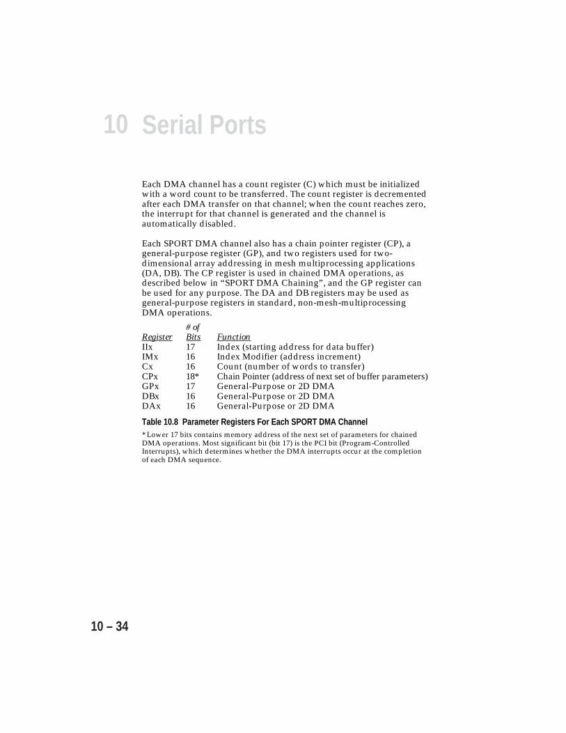
10 Serial Ports
10 – 34
Each DMA channel has a count register (C) which must be initializedwith a word count to be transferred. The count register is decrementedafter each DMA transfer on that channel; when the count reaches zero,the interrupt for that channel is generated and the channel isautomatically disabled.
Each SPORT DMA channel also has a chain pointer register (CP), ageneral-purpose register (GP), and two registers used for two-dimensional array addressing in mesh multiprocessing applications(DA, DB). The CP register is used in chained DMA operations, asdescribed below in “SPORT DMA Chaining”, and the GP register canbe used for any purpose. The DA and DB registers may be used asgeneral-purpose registers in standard, non-mesh-multiprocessingDMA operations.
# ofRegister Bits FunctionIIx 17 Index (starting address for data buffer)IMx 16 Index Modifier (address increment)Cx 16 Count (number of words to transfer)CPx 18* Chain Pointer (address of next set of buffer parameters)GPx 17 General-Purpose or 2D DMADBx 16 General-Purpose or 2D DMADAx 16 General-Purpose or 2D DMA
Table 10.8 Parameter Registers For Each SPORT DMA Channel* Lower 17 bits contains memory address of the next set of parameters for chainedDMA operations. Most significant bit (bit 17) is the PCI bit (Program-ControlledInterrupts), which determines whether the DMA interrupts occur at the completionof each DMA sequence.
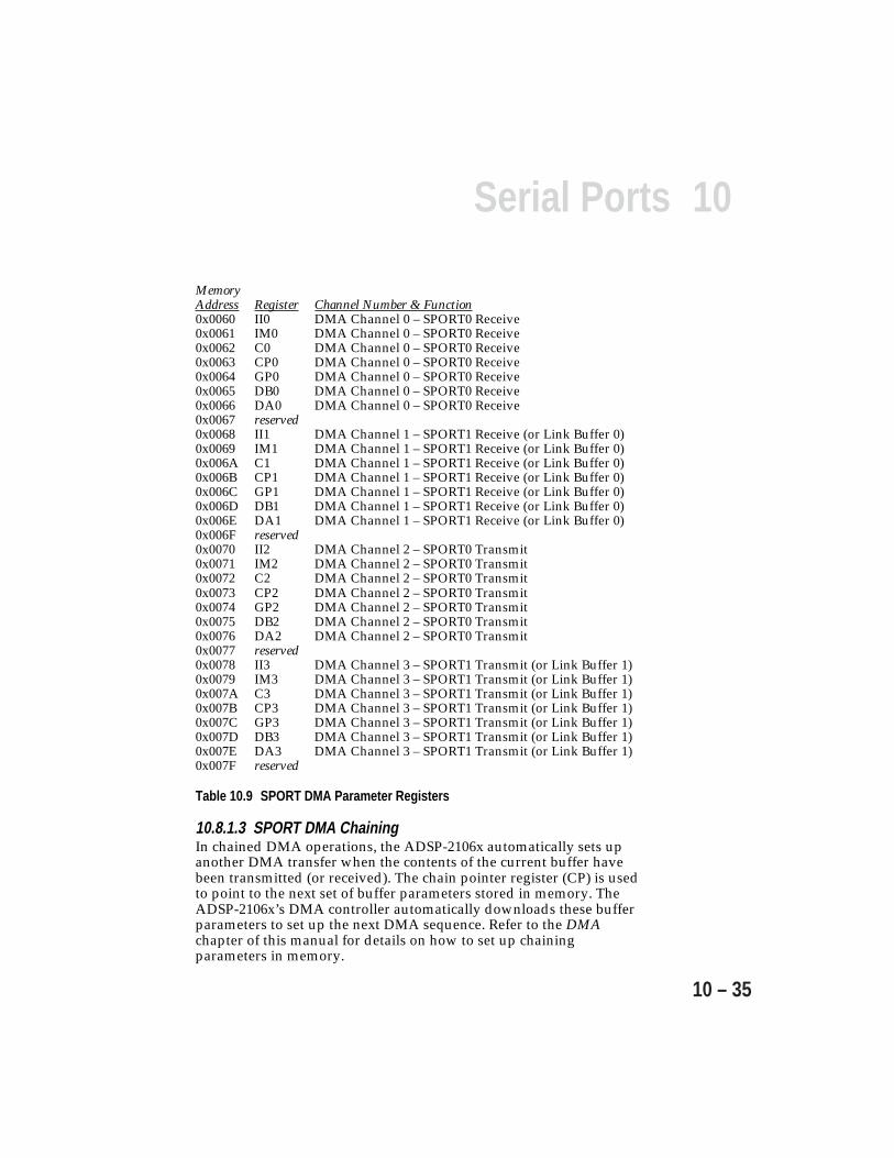
10Serial Ports
10 – 35
MemoryAddress Register Channel Number & Function0x0060 II0 DMA Channel 0 – SPORT0 Receive0x0061 IM0 DMA Channel 0 – SPORT0 Receive0x0062 C0 DMA Channel 0 – SPORT0 Receive0x0063 CP0 DMA Channel 0 – SPORT0 Receive0x0064 GP0 DMA Channel 0 – SPORT0 Receive0x0065 DB0 DMA Channel 0 – SPORT0 Receive0x0066 DA0 DMA Channel 0 – SPORT0 Receive0x0067 reserved0x0068 II1 DMA Channel 1 – SPORT1 Receive (or Link Buffer 0)0x0069 IM1 DMA Channel 1 – SPORT1 Receive (or Link Buffer 0)0x006A C1 DMA Channel 1 – SPORT1 Receive (or Link Buffer 0)0x006B CP1 DMA Channel 1 – SPORT1 Receive (or Link Buffer 0)0x006C GP1 DMA Channel 1 – SPORT1 Receive (or Link Buffer 0)0x006D DB1 DMA Channel 1 – SPORT1 Receive (or Link Buffer 0)0x006E DA1 DMA Channel 1 – SPORT1 Receive (or Link Buffer 0)0x006F reserved0x0070 II2 DMA Channel 2 – SPORT0 Transmit0x0071 IM2 DMA Channel 2 – SPORT0 Transmit0x0072 C2 DMA Channel 2 – SPORT0 Transmit0x0073 CP2 DMA Channel 2 – SPORT0 Transmit0x0074 GP2 DMA Channel 2 – SPORT0 Transmit0x0075 DB2 DMA Channel 2 – SPORT0 Transmit0x0076 DA2 DMA Channel 2 – SPORT0 Transmit0x0077 reserved0x0078 II3 DMA Channel 3 – SPORT1 Transmit (or Link Buffer 1)0x0079 IM3 DMA Channel 3 – SPORT1 Transmit (or Link Buffer 1)0x007A C3 DMA Channel 3 – SPORT1 Transmit (or Link Buffer 1)0x007B CP3 DMA Channel 3 – SPORT1 Transmit (or Link Buffer 1)0x007C GP3 DMA Channel 3 – SPORT1 Transmit (or Link Buffer 1)0x007D DB3 DMA Channel 3 – SPORT1 Transmit (or Link Buffer 1)0x007E DA3 DMA Channel 3 – SPORT1 Transmit (or Link Buffer 1)0x007F reserved
Table 10.9 SPORT DMA Parameter Registers
10.8.1.3 SPORT DMA ChainingIn chained DMA operations, the ADSP-2106x automatically sets upanother DMA transfer when the contents of the current buffer havebeen transmitted (or received). The chain pointer register (CP) is usedto point to the next set of buffer parameters stored in memory. TheADSP-2106x’s DMA controller automatically downloads these bufferparameters to set up the next DMA sequence. Refer to the DMAchapter of this manual for details on how to set up chainingparameters in memory.
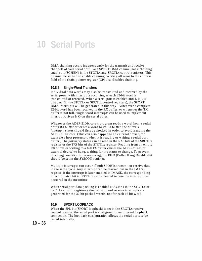
10 Serial Ports
10 – 36
DMA chaining occurs independently for the transmit and receivechannels of each serial port. Each SPORT DMA channel has a chainingenable bit (SCHEN) in the STCTLx and SRCTLx control registers. Thisbit must be set to 1 to enable chaining. Writing all zeros to the addressfield of the chain pointer register (CP) also disables chaining.
10.8.2 Single-Word TransfersIndividual data words may also be transmitted and received by theserial ports, with interrupts occurring as each 32-bit word istransmitted or received. When a serial port is enabled and DMA isdisabled (in the STCTLx or SRCTLx control registers), the SPORTDMA interrupts will be generated in this way—whenever a complete32-bit word has been received in the RX buffer, or whenever the TXbuffer is not full. Single-word interrupts can be used to implementinterrupt-driven I/O on the serial ports.
Whenever the ADSP-2106x core’s program reads a word from a serialport’s RX buffer or writes a word to its TX buffer, the buffer’sfull/empty status should first be checked in order to avoid hanging theADSP-2106x core. (This can also happen to an external device, forexample a host processor, when it is reading or writing a serial portbuffer.) The full/empty status can be read in the RXS bits of the SRCTLxregister or the TXS bits of the STCTLx register. Reading from an emptyRX buffer or writing to a full TX buffer causes the ADSP-2106x (orexternal device) to hang, waiting for the status to change. To preventthis hang condition from occurring, the BHD (Buffer Hang Disable) bitshould be set in the SYSCON register.
Multiple interrupts can occur if both SPORTs transmit or receive datain the same cycle. Any interrupt can be masked out in the IMASKregister; if the interrupt is later enabled in IMASK, the correspondinginterrupt latch bit in IRPTL must be cleared in case the interrupt hasoccurred in the meantime.
When serial port data packing is enabled (PACK=1 in the STCTLx orSRCTLx control registers), the transmit and receive interrupts aregenerated for the 32-bit packed words, not for each 16-bit word.
10.9 SPORT LOOPBACKWhen the SPL bit (SPORT loopback) is set in the SRCTLx receivecontrol register, the serial port is configured in an internal loopbackconnection. The loopback configuration allows the serial ports to betested internally.
10Serial Ports
10 – 37
When loopback is configured, the DRx, RCLKx, and RFSx signals ofthe receive section of the SPORT are internally connected to the DTx,TCLKx, and TFSx signals of the transmit section. The DTx, TCLKx, andTFSx signals are active and are available at their respective pins, whilethe DRx, RCLKx, and RFSx pins are ignored by the ADSP-2106x.
Only transmit clock and transmit frame sync options may be used inloopback mode—you must ensure that the serial port is set upcorrectly in the STCTLx and SRCTLx control registers. Multichannelmode is not allowed.
10.10 SPORT PIN DRIVER CONCERNSThe ADSP-2106x has very fast drivers on all output pins including theserial ports. If connections on the data, clock, or frame sync lines arelonger than six inches, you should consider using a series terminationfor strip lines on point-to-point connections. This may be necessaryeven when using low-speed serial clocks, because of the edge rates.
10.11 SPORT PROGRAMMING EXAMPLESThere are three ways to control serial port communications andmemory-to-SPORT data transfers: single-word transfers under coreprocessor control with no interrupts, single-word transfers under coreprocessor control with interrupts, and DMA transfers with interrupts.The three examples presented below illustrate each of these methods.In each example, the SPORT0 is used to transmit eight 32-bit wordsfrom a data buffer in internal memory.
Any of the three control schemes may be used in multichannel modeand with any of the serial clock and frame sync options.
10.11.1 Single-Word Transfers Without InterruptsThe ADSP-2106x processor core will stall (i.e. hang) when it attemptsto write data to a full TX buffer or read data from an empty RX buffer.This provides a very simple method of controlling the SPORT—placing the instruction that writes data to TX or reads data from RX ina loop. Program execution will stall at this instruction, until the SPORTis ready to transmit new data or has received new data.
Listing 10.1 shows the code for this example, which sets up a loop totransmit data out of SPORT0. Although this technique provides a verysimple programming solution, it prevents the ADSP-2106x processorcore from handling any other tasks while waiting for the serial port.The interrupt-driven technique described in the following sectionalleviates this.
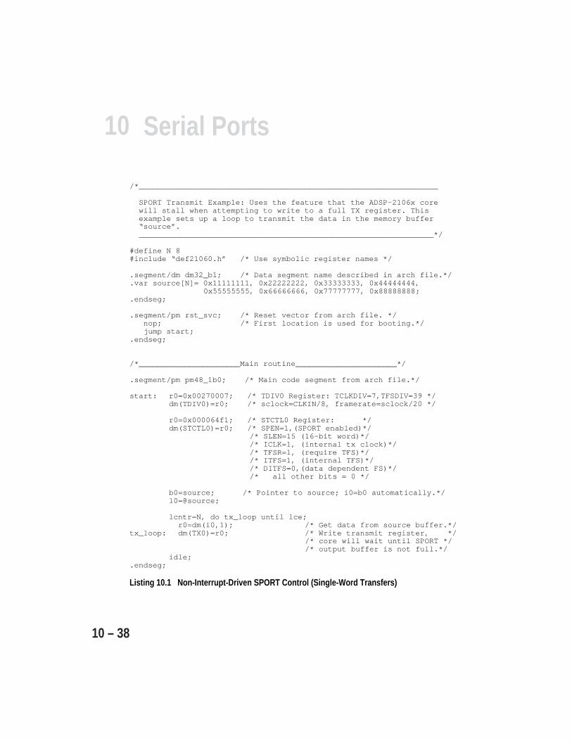
10 Serial Ports
10 – 38
/*_________________________________________________________________
SPORT Transmit Example: Uses the feature that the ADSP-2106x core will stall when attempting to write to a full TX register. This example sets up a loop to transmit the data in the memory buffer “source”. ________________________________________________________________*/
#define N 8#include “def21060.h” /* Use symbolic register names */
.segment/dm dm32_b1; /* Data segment name described in arch file.*/
.var source[N]= 0x11111111, 0x22222222, 0x33333333, 0x44444444,0x55555555, 0x66666666, 0x77777777, 0x88888888;
.endseg;
.segment/pm rst_svc; /* Reset vector from arch file. */ nop; /* First location is used for booting.*/ jump start;.endseg;
/*______________________Main routine______________________*/
.segment/pm pm48_1b0; /* Main code segment from arch file.*/
start: r0=0x00270007; /* TDIV0 Register: TCLKDIV=7,TFSDIV=39 */dm(TDIV0)=r0; /* sclock=CLKIN/8, framerate=sclock/20 */
r0=0x000064f1; /* STCTL0 Register: */dm(STCTL0)=r0; /* SPEN=1,(SPORT enabled)*/
/* SLEN=15 (16-bit word)*/ /* ICLK=1, (internal tx clock)*/ /* TFSR=1, (require TFS)*/ /* ITFS=1, (internal TFS)*/ /* DITFS=0,(data dependent FS)*/ /* all other bits = 0 */
b0=source; /* Pointer to source; i0=b0 automatically.*/l0=@source;
lcntr=N, do tx_loop until lce; r0=dm(i0,1); /* Get data from source buffer.*/
tx_loop: dm(TX0)=r0; /* Write transmit register, */ /* core will wait until SPORT */ /* output buffer is not full.*/
idle;.endseg;
Listing 10.1 Non-Interrupt-Driven SPORT Control (Single-Word Transfers)
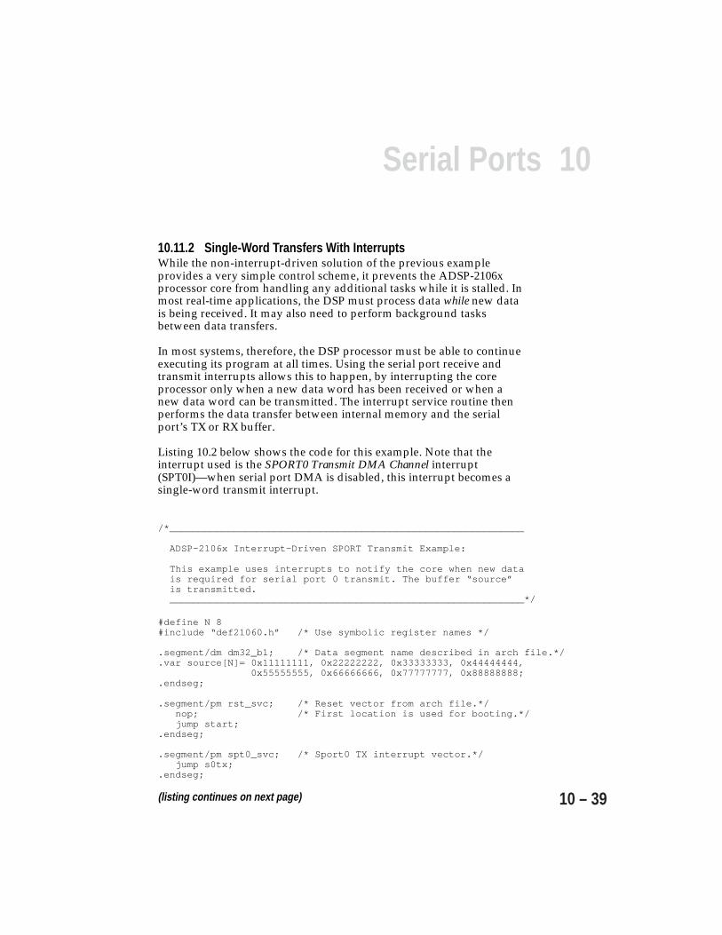
10Serial Ports
10 – 39
/*_____________________________________________________________
ADSP-2106x Interrupt-Driven SPORT Transmit Example:
This example uses interrupts to notify the core when new data is required for serial port 0 transmit. The buffer “source” is transmitted. _____________________________________________________________*/
#define N 8#include “def21060.h” /* Use symbolic register names */
.segment/dm dm32_b1; /* Data segment name described in arch file.*/
.var source[N]= 0x11111111, 0x22222222, 0x33333333, 0x44444444,0x55555555, 0x66666666, 0x77777777, 0x88888888;
.endseg;
.segment/pm rst_svc; /* Reset vector from arch file.*/ nop; /* First location is used for booting.*/ jump start;.endseg;
.segment/pm spt0_svc; /* Sport0 TX interrupt vector.*/ jump s0tx;.endseg;
(listing continues on next page)
10.11.2 Single-Word Transfers With InterruptsWhile the non-interrupt-driven solution of the previous exampleprovides a very simple control scheme, it prevents the ADSP-2106xprocessor core from handling any additional tasks while it is stalled. Inmost real-time applications, the DSP must process data while new datais being received. It may also need to perform background tasksbetween data transfers.
In most systems, therefore, the DSP processor must be able to continueexecuting its program at all times. Using the serial port receive andtransmit interrupts allows this to happen, by interrupting the coreprocessor only when a new data word has been received or when anew data word can be transmitted. The interrupt service routine thenperforms the data transfer between internal memory and the serialport’s TX or RX buffer.
Listing 10.2 below shows the code for this example. Note that theinterrupt used is the SPORT0 Transmit DMA Channel interrupt(SPT0I)—when serial port DMA is disabled, this interrupt becomes asingle-word transmit interrupt.

10 Serial Ports
10 – 40
/*_________________________Main routine_________________________*/
.segment/pm pm48_1b0; /* Main code segment from arch file.*/
start: r0=0x00270007; /* TDIV0 Register: TCLKDIV=7,TFSDIV=39 */dm(TDIV0)=r0; /* sclock=CLKIN/8, framerate=sclock/20 */
r0=0x000064f1; /* STCTL0 Register: */dm(STCTL0)=r0; /* SPEN=1,(SPORT enabled)*/
/* SLEN=15 (16-bit word)*/ /* ICLK=1, (internal tx clock)*/ /* TFSR=1, (require TFS)*/ /* ITFS=1, (internal TFS)*/ /* DITFS=0,(data dependent FS)*/ /* all other bits = 0 */
b0=source; /* Pointer to source; i0=b0 automatically.*/l0=@source;
bit set imask SPT0I; /* Enable Sport0 TX interrupt.*/bit set mode1 IRPTEN; /* Global interrupt enable.*/
r0=dm(i0,1); /* Write first value into TX0 to kick off sport.*/dm(TX0)=r0;
wait: idle; /* Wait for SPORT0 TX interrupts.*/jump wait;
/*_____________SPORT0 Transmit Interrupt Routine_______________*/
s0tx: rti (db);r0=dm(i0,1); /* Get data from source buffer */dm(TX0)=r0; /* Write transmit register */
.endseg;
Listing 10.2 Interrupt-Driven SPORT Control (Single-Word Transfers)
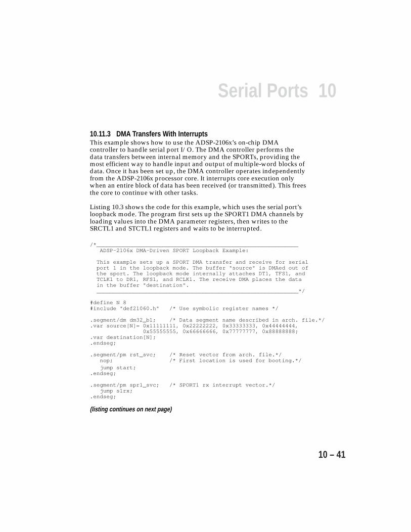
10Serial Ports
10 – 41
/*_____________________________________________________________ ADSP-2106x DMA-Driven SPORT Loopback Example:
This example sets up a SPORT DMA transfer and receive for serialport 1 in the loopback mode. The buffer "source" is DMAed out ofthe sport. The loopback mode internally attaches DT1, TFS1, andTCLK1 to DR1, RFS1, and RCLK1. The receive DMA places the datain the buffer "destination".
_____________________________________________________________*/
#define N 8#include "def21060.h" /* Use symbolic register names */
.segment/dm dm32_b1; /* Data segment name described in arch. file.*/
.var source[N]= 0x11111111, 0x22222222, 0x33333333, 0x44444444, 0x55555555, 0x66666666, 0x77777777, 0x88888888;.var destination[N];.endseg;
.segment/pm rst_svc; /* Reset vector from arch. file.*/ nop; /* First location is used for booting.*/ jump start;.endseg;
.segment/pm spr1_svc; /* SPORT1 rx interrupt vector.*/ jump s1rx;.endseg;
(listing continues on next page)
10.11.3 DMA Transfers With InterruptsThis example shows how to use the ADSP-2106x’s on-chip DMAcontroller to handle serial port I/O. The DMA controller performs thedata transfers between internal memory and the SPORTs, providing themost efficient way to handle input and output of multiple-word blocks ofdata. Once it has been set up, the DMA controller operates independentlyfrom the ADSP-2106x processor core. It interrupts core execution onlywhen an entire block of data has been received (or transmitted). This freesthe core to continue with other tasks.
Listing 10.3 shows the code for this example, which uses the serial port’sloopback mode. The program first sets up the SPORT1 DMA channels byloading values into the DMA parameter registers, then writes to theSRCTL1 and STCTL1 registers and waits to be interrupted.
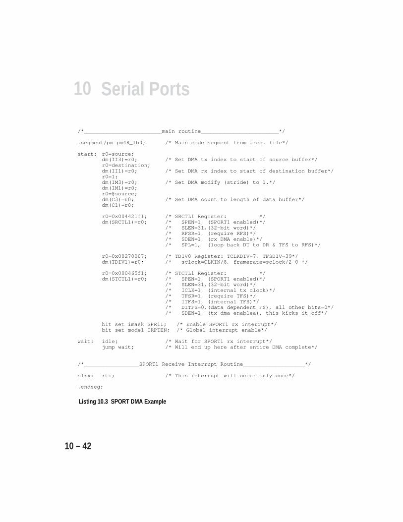
10 Serial Ports
10 – 42
/*________________________main routine________________________*/
.segment/pm pm48_1b0; /* Main code segment from arch. file*/
start: r0=source;dm(II3)=r0; /* Set DMA tx index to start of source buffer*/r0=destination;dm(II1)=r0; /* Set DMA rx index to start of destination buffer*/r0=1;dm(IM3)=r0; /* Set DMA modify (stride) to 1.*/dm(IM1)=r0;r0=@source;dm(C3)=r0; /* Set DMA count to length of data buffer*/dm(C1)=r0;
r0=0x004421f1; /* SRCTL1 Register: */dm(SRCTL1)=r0; /* SPEN=1, (SPORT1 enabled)*/
/* SLEN=31,(32-bit word)*//* RFSR=1, (require RFS)*//* SDEN=1, (rx DMA enable)*//* SPL=1, (loop back DT to DR & TFS to RFS)*/
r0=0x00270007; /* TDIV0 Register: TCLKDIV=7, TFSDIV=39*/dm(TDIV1)=r0; /* sclock=CLKIN/8, framerate=sclock/2 0 */
r0=0x000465f1; /* STCTL1 Register: */dm(STCTL1)=r0; /* SPEN=1, (SPORT1 enabled)*/
/* SLEN=31,(32-bit word)*//* ICLK=1, (internal tx clock)*//* TFSR=1, (require TFS)*//* ITFS=1, (internal TFS)*//* DITFS=0,(data dependent FS), all other bits=0*//* SDEN=1, (tx dma enablea), this kicks it off*/
bit set imask SPR1I; /* Enable SPORT1 rx interrupt*/bit set mode1 IRPTEN; /* Global interrupt enable*/
wait: idle; /* Wait for SPORT1 rx interrupt*/jump wait; /* Will end up here after entire DMA complete*/
/*_________________SPORT1 Receive Interrupt Routine___________________*/
s1rx: rti; /* This interrupt will occur only once*/
.endseg;
Listing 10.3 SPORT DMA Example

11
11 – 1
System Design
11.1 OVERVIEWThis chapter provides hardware, software, and system designinformation.
11.2 ADSP-2106X PINSThis section describes the pins of the ADSP-2106x and shows howthese signals can be used in your system. Figure 11.1 illustrates howthe pins are used in a single-processor system. Figure 7.1 in theMultiprocessing chapter shows a system diagram illustrating pinconnections in an ADSP-2106x multiprocessor cluster.
Figure 11.1 Basic ADSP-2106x System
ADDR
DATA
BOOT EPROM
CLKIN
RESET
IRQ2-0
EBOOTLBOOT
FLAG 3-0
DMAR1-2DMAG1-2
LxCLKLxACKLxDAT3-0
TIMEXP
RPBAID2-0
BMS
ADSP-2106x
ADDR
DATA
DATA
ADDR
DATA
ADDR31-0
DATA47-0
CS
MEMORY & PERIPHERALS
DMA DEVICE
(OPTIONAL)
LINK DEVICES(6 Maximum)(OPTIONAL)
(OPTIONAL)
SERIALDEVICE
(OPTIONAL)
(OPTIONAL)
(OPTIONAL)
JTAG
ADDR
ESS
DATA
CONT
ROL
7
4
3
SERIALDEVICE
(OPTIONAL)
HOSTPROCESSORINTERFACE
BR1-6
1x CLOCK
CPA
OEWEACKCS
RDWRACKMS3-0
PAGESBTS
SWADRCLK
CSHBRHBG
REDY
TCLK1RCLK1TFS1RFS1DT1DR1
TCLK0RCLK0TFS0RFS0DT0DR0
11 System Design
11 – 2
11.2.1 Pin DefinitionsADSP-2106x pin definitions are listed below. All pins are identical onthe ADSP-21060 and ADSP-21062. Inputs identified as synchronous (S)must meet timing requirements with respect to CLKIN (or with respectto TCK for TMS, TDI). Inputs identified as asynchronous (A) can beasserted asynchronously to CLKIN (or to TCK for TRST).
Unused inputs should be tied or pulled to VDD or GND, except forADDR31-0, DATA47-0, FLAG3-0, SW, and inputs that have internalpullup or pulldown resistors (CPA, ACK, DTx, DRx, TCLKx, RCLKx,LxDAT3-0, LxCLK, LxACK, TMS, and TDI)—these pins should be leftfloating. These pins have a logic-level hold circuit that prevents theinput from floating internally.
I=Input S=Synchronous P=Power Supply (o/d)=Open DrainO=Output A=Asynchronous G=Ground (a/d)=Active Drive
T=Three-State (when SBTS is asserted, or when the ADSP-2106x is a bus slave)
Pin Type FunctionADDR31-0 I/O/T External Bus Address. The ADSP-2106x outputs addresses for
external memory and peripherals on these pins. In amultiprocessor system, the bus master outputs addresses forread/writes of the internal memory or IOP registers of otherADSP-2106xs. The ADSP-2106x inputs addresses when a hostprocessor or multiprocessing bus master is reading or writingits internal memory or IOP registers.
DATA47-0 I/O/T External Bus Data. The ADSP-2106x inputs and outputs dataand instructions on these pins. 32-bit single-precision floating-point data and 32-bit fixed-point data is transferred over bits47-16 of the bus. 40-bit extended-precision floating-point data istransferred over bits 47-8 of the bus. 16-bit short word data istransferred over bits 31-16 of the bus. In PROM boot mode,8-bit data is transferred over bits 23-16. Pull-up resistors onunused DATA pins are not necessary.
MS3-0 O/T Memory Select Lines. These lines are asserted (low) as chipselects for the corresponding banks of external memory.Memory bank size must be defined in the ADSP-2106x’s systemcontrol register (SYSCON). The MS3-0 lines are decodedmemory address lines that change at the same time as the otheraddress lines. When no external memory access is occurring theMS3-0 lines are inactive; they are active, however, when aconditional memory access instruction is executed, whether ornot the condition is true. MS0 can be used with the PAGE signalto implement a bank of DRAM memory (Bank 0). In amultiprocessing system, the MS3-0 lines are output by the busmaster.
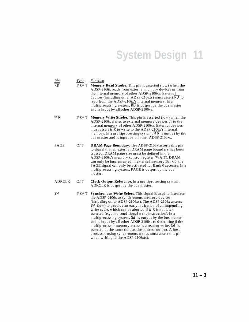
11System Design
11 – 3
Pin Type FunctionRD I/O/T Memory Read Strobe. This pin is asserted (low) when the
ADSP-2106x reads from external memory devices or fromthe internal memory of other ADSP-2106xs. Externaldevices (including other ADSP-2106xs) must assert RD toread from the ADSP-2106x’s internal memory. In amultiprocessing system, RD is output by the bus masterand is input by all other ADSP-2106xs.
WR I/O/T Memory Write Strobe. This pin is asserted (low) when theADSP-2106x writes to external memory devices or to theinternal memory of other ADSP-2106xs. External devicesmust assert WR to write to the ADSP-2106x’s internalmemory. In a multiprocessing system, WR is output by thebus master and is input by all other ADSP-2106xs.
PAGE O/T DRAM Page Boundary. The ADSP-2106x asserts this pinto signal that an external DRAM page boundary has beencrossed. DRAM page size must be defined in theADSP-2106x’s memory control register (WAIT). DRAMcan only be implemented in external memory Bank 0; thePAGE signal can only be activated for Bank 0 accesses. In amultiprocessing system, PAGE is output by the busmaster.
ADRCLK O/T Clock Output Reference. In a multiprocessing system,ADRCLK is output by the bus master.
SW I/O/T Synchronous Write Select. This signal is used to interfacethe ADSP-2106x to synchronous memory devices(including other ADSP-2106xs). The ADSP-2106x assertsSW (low) to provide an early indication of an impendingwrite cycle, which can be aborted if WR is not laterasserted (e.g. in a conditional write instruction). In amultiprocessing system, SW is output by the bus masterand is input by all other ADSP-2106xs to determine if themultiprocessor memory access is a read or write. SW isasserted at the same time as the address output. A hostprocessor using synchronous writes must assert this pinwhen writing to the ADSP-2106x(s).
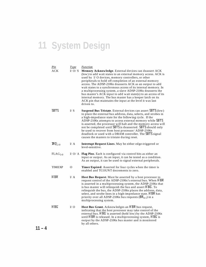
11 System Design
11 – 4
Pin Type FunctionACK I/O/S Memory Acknowledge. External devices can deassert ACK
(low) to add wait states to an external memory access. ACK isused by I/O devices, memory controllers, or otherperipherals to hold off completion of an external memoryaccess. The ADSP-2106x deasserts ACK as an output to addwait states to a synchronous access of its internal memory. Ina multiprocessing system, a slave ADSP-2106x deasserts thebus master’s ACK input to add wait state(s) to an access of itsinternal memory. The bus master has a keeper latch on itsACK pin that maintains the input at the level it was lastdriven to.
SBTS I/S Suspend Bus Tristate. External devices can assert SBTS (low)to place the external bus address, data, selects, and strobes ina high-impedance state for the following cycle. If theADSP-2106x attempts to access external memory while SBTSis asserted, the processor will halt and the memory access willnot be completed until SBTS is deasserted. SBTS should onlybe used to recover from host processor/ADSP-2106xdeadlock or used with a DRAM controller. The SBTS signalcauses the masters to tristate during reset.
IRQ2-0 I/A Interrupt Request Lines. May be either edge-triggered orlevel-sensitive.
FLAG3-0 I/O/A Flag Pins. Each is configured via control bits as either aninput or output. As an input, it can be tested as a condition.As an output, it can be used to signal external peripherals.
TIMEXP O Timer Expired. Asserted for four cycles when the timer isenabled and TCOUNT decrements to zero.
HBR I/A Host Bus Request. Must be asserted by a host processor torequest control of the ADSP-2106x’s external bus. When HBRis asserted in a multiprocessing system, the ADSP-2106x thatis bus master will relinquish the bus and assert HBG. Torelinquish the bus, the ADSP-2106x places the address, data,select, and strobe lines in a high-impedance state. HBR haspriority over all ADSP-2106x bus requests (BR6-1) in amultiprocessing system.
HBG I/O Host Bus Grant. Acknowledges an HBR bus request,indicating that the host processor may take control of theexternal bus. HBG is asserted (held low) by the ADSP-2106xuntil HBR is released. In a multiprocessing system, HBG isoutput by the ADSP-2106x bus master and is monitoredby all others.
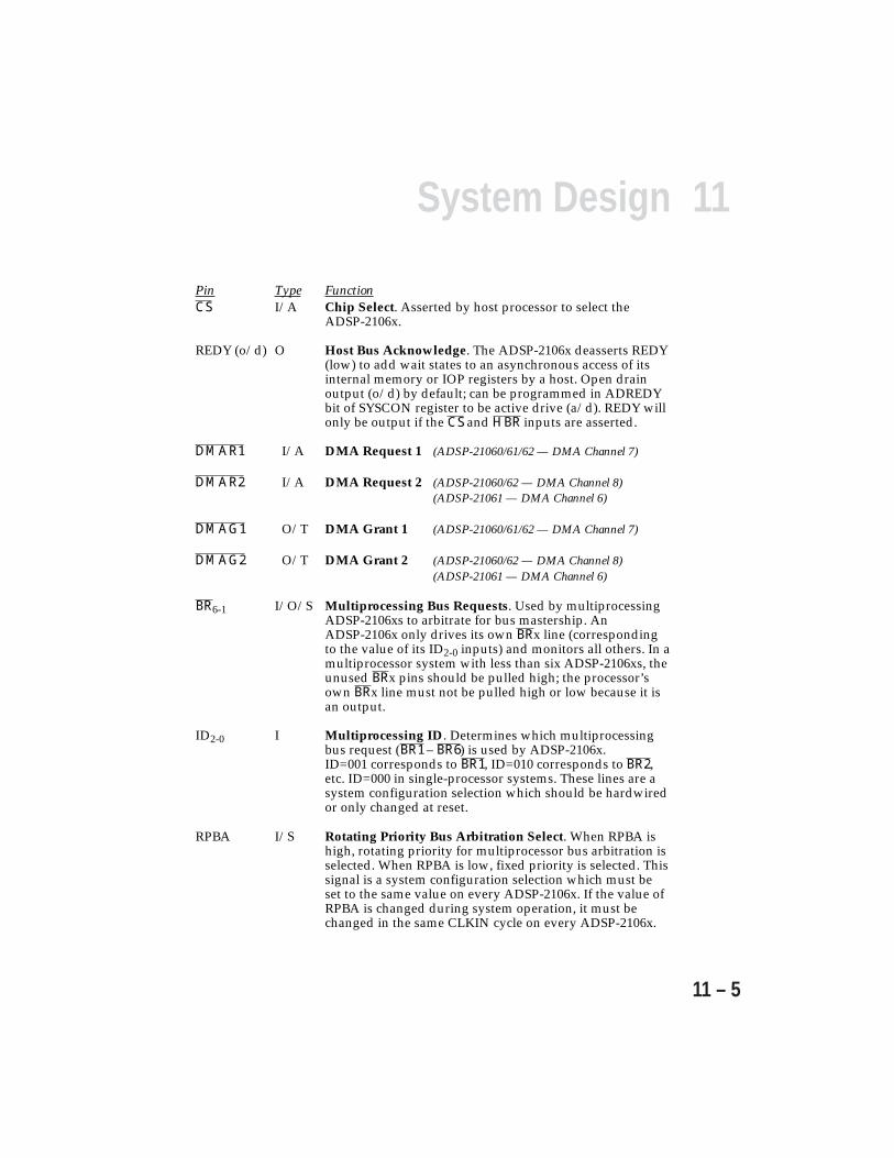
11System Design
11 – 5
Pin Type FunctionCS I/A Chip Select. Asserted by host processor to select the
ADSP-2106x.
REDY (o/d) O Host Bus Acknowledge. The ADSP-2106x deasserts REDY(low) to add wait states to an asynchronous access of itsinternal memory or IOP registers by a host. Open drainoutput (o/d) by default; can be programmed in ADREDYbit of SYSCON register to be active drive (a/d). REDY willonly be output if the CS and HBR inputs are asserted.
DMAR1 I/A DMA Request 1 (ADSP-21060/61/62 — DMA Channel 7)
DMAR2 I/A DMA Request 2 (ADSP-21060/62 — DMA Channel 8)(ADSP-21061 — DMA Channel 6)
DMAG1 O/T DMA Grant 1 (ADSP-21060/61/62 — DMA Channel 7)
DMAG2 O/T DMA Grant 2 (ADSP-21060/62 — DMA Channel 8)(ADSP-21061 — DMA Channel 6)
BR6-1 I/O/S Multiprocessing Bus Requests. Used by multiprocessingADSP-2106xs to arbitrate for bus mastership. AnADSP-2106x only drives its own BRx line (correspondingto the value of its ID2-0 inputs) and monitors all others. In amultiprocessor system with less than six ADSP-2106xs, theunused BRx pins should be pulled high; the processor’sown BRx line must not be pulled high or low because it isan output.
ID2-0 I Multiprocessing ID. Determines which multiprocessingbus request (BR1 – BR6) is used by ADSP-2106x.ID=001 corresponds to BR1, ID=010 corresponds to BR2,etc. ID=000 in single-processor systems. These lines are asystem configuration selection which should be hardwiredor only changed at reset.
RPBA I/S Rotating Priority Bus Arbitration Select. When RPBA ishigh, rotating priority for multiprocessor bus arbitration isselected. When RPBA is low, fixed priority is selected. Thissignal is a system configuration selection which must beset to the same value on every ADSP-2106x. If the value ofRPBA is changed during system operation, it must bechanged in the same CLKIN cycle on every ADSP-2106x.
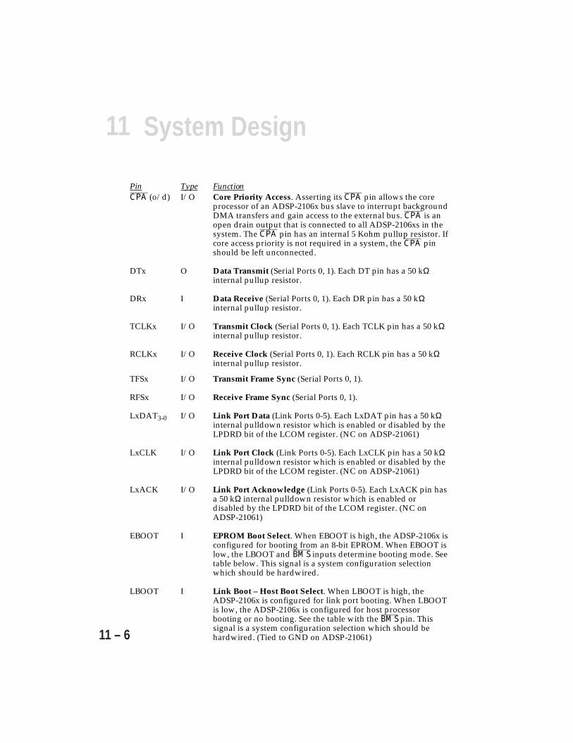
11 System Design
11 – 6
Pin Type FunctionCPA (o/d) I/O Core Priority Access. Asserting its CPA pin allows the core
processor of an ADSP-2106x bus slave to interrupt backgroundDMA transfers and gain access to the external bus. CPA is anopen drain output that is connected to all ADSP-2106xs in thesystem. The CPA pin has an internal 5 Kohm pullup resistor. Ifcore access priority is not required in a system, the CPA pinshould be left unconnected.
DTx O Data Transmit (Serial Ports 0, 1). Each DT pin has a 50 kΩinternal pullup resistor.
DRx I Data Receive (Serial Ports 0, 1). Each DR pin has a 50 kΩinternal pullup resistor.
TCLKx I/O Transmit Clock (Serial Ports 0, 1). Each TCLK pin has a 50 kΩinternal pullup resistor.
RCLKx I/O Receive Clock (Serial Ports 0, 1). Each RCLK pin has a 50 kΩinternal pullup resistor.
TFSx I/O Transmit Frame Sync (Serial Ports 0, 1).
RFSx I/O Receive Frame Sync (Serial Ports 0, 1).
LxDAT3-0 I/O Link Port Data (Link Ports 0-5). Each LxDAT pin has a 50 kΩinternal pulldown resistor which is enabled or disabled by theLPDRD bit of the LCOM register. (NC on ADSP-21061)
LxCLK I/O Link Port Clock (Link Ports 0-5). Each LxCLK pin has a 50 kΩinternal pulldown resistor which is enabled or disabled by theLPDRD bit of the LCOM register. (NC on ADSP-21061)
LxACK I/O Link Port Acknowledge (Link Ports 0-5). Each LxACK pin hasa 50 kΩ internal pulldown resistor which is enabled ordisabled by the LPDRD bit of the LCOM register. (NC onADSP-21061)
EBOOT I EPROM Boot Select. When EBOOT is high, the ADSP-2106x isconfigured for booting from an 8-bit EPROM. When EBOOT islow, the LBOOT and BMS inputs determine booting mode. Seetable below. This signal is a system configuration selectionwhich should be hardwired.
LBOOT I Link Boot – Host Boot Select. When LBOOT is high, theADSP-2106x is configured for link port booting. When LBOOTis low, the ADSP-2106x is configured for host processorbooting or no booting. See the table with the BMS pin. Thissignal is a system configuration selection which should behardwired. (Tied to GND on ADSP-21061)
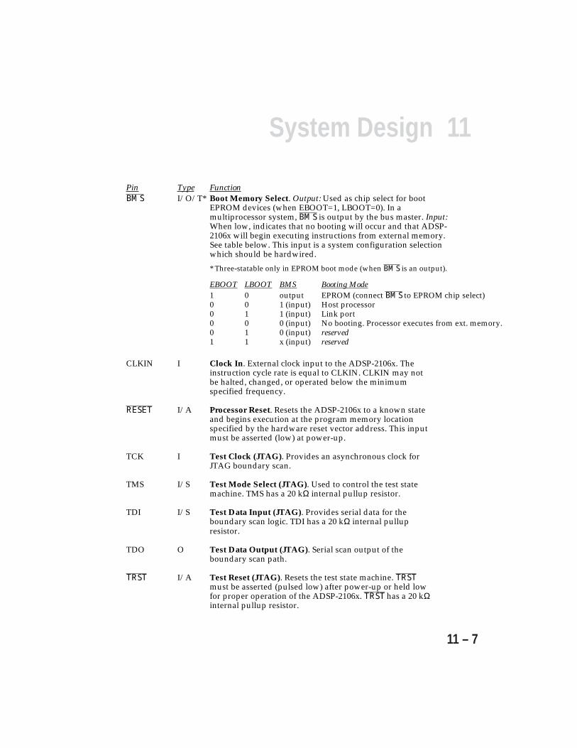
11System Design
11 – 7
Pin Type FunctionBMS I/O/T* Boot Memory Select. Output: Used as chip select for boot
EPROM devices (when EBOOT=1, LBOOT=0). In amultiprocessor system, BMS is output by the bus master. Input:When low, indicates that no booting will occur and that ADSP-2106x will begin executing instructions from external memory.See table below. This input is a system configuration selectionwhich should be hardwired.
* Three-statable only in EPROM boot mode (when BMS is an output).
EBOOT LBOOT BMS Booting Mode1 0 output EPROM (connect BMS to EPROM chip select)0 0 1 (input) Host processor0 1 1 (input) Link port0 0 0 (input) No booting. Processor executes from ext. memory.0 1 0 (input) reserved1 1 x (input) reserved
CLKIN I Clock In. External clock input to the ADSP-2106x. Theinstruction cycle rate is equal to CLKIN. CLKIN may notbe halted, changed, or operated below the minimumspecified frequency.
RESET I/A Processor Reset. Resets the ADSP-2106x to a known stateand begins execution at the program memory locationspecified by the hardware reset vector address. This inputmust be asserted (low) at power-up.
TCK I Test Clock (JTAG). Provides an asynchronous clock forJTAG boundary scan.
TMS I/S Test Mode Select (JTAG). Used to control the test statemachine. TMS has a 20 kΩ internal pullup resistor.
TDI I/S Test Data Input (JTAG). Provides serial data for theboundary scan logic. TDI has a 20 kΩ internal pullupresistor.
TDO O Test Data Output (JTAG). Serial scan output of theboundary scan path.
TRST I/A Test Reset (JTAG). Resets the test state machine. TRSTmust be asserted (pulsed low) after power-up or held lowfor proper operation of the ADSP-2106x. TRST has a 20 kΩinternal pullup resistor.

11 System Design
11 – 8
Pin Type FunctionEMU O Emulation Status. Must be connected to the ADSP-2106x EZ-ICE
target board connector only.
ICSA O Reserved, leave unconnected.
VDD P Power Supply; nominally +5.0V dc for 5V devices or +3.3V dc for3.3V devcies. (30 pins)
GND G Power Supply Return. (30 pins)
NC Do Not Connect. Reserved pins which must be left open andunconnected. Note that the LxDAT, LxCLK, and LxACK pins onthe ADSP-21060 and ADSP-21062 are NC on the ADSP-21061.
THE TRST INPUT OF THE JTAG INTERFACE MUST BE ASSERTED(I.E. PULSED LOW) OR HELD LOW AFTER POWER-UP FOR PROPEROPERATION OF THE ADSP-2106X. DO NOT LEAVE THIS PIN UNCONNECTED!!
Additional Notes:
• In single-processor systems, the ADSP-2106x owns the external bus duringreset and does not perform bus arbitration to gain control of the bus.
• Operation of the RD and WR signals changes when CS is asserted by a hostprocessor. See “Asynchronous Transfers” and “Synchronous Transfers” inthe Host Interface chapter for details.
• Except during a Host Transition Cycle (HTC), the RD and WR strobesshould not be deasserted (low-to-high transition) while ACK or REDY aredeasserted (low )—the ADSP-2106x will hang if this happens.
• In multiprocessor systems, the ACK signal is an input to the ADSP-2106xbus master and will not float when it is not being driven (because the busmaster maintains a weak keeper latch on the pin). During reset, the ACK pinis pulled high internally with a 2 kΩ equivalent resistor by the ADSP-2106xbus master and is held high with the internal keeper latch. It is not necessaryto use an external pullup resistor on the ACK line during booting or at anyother time.
• For multiprocessor systems, PAGE is guaranteed to be asserted for the firsttrue access after acquiring bus mastership. PAGE will not be updated orasserted for multiprocessor memory space accesses or external memory spaceaccesses to any bank other than Bank 0.
• The HBR input is disabled during any access in which the PAGE signal isasserted. This prevents the possibility of the ADSP-2106x becoming a busslave while a DRAM controller is servicing a page change.
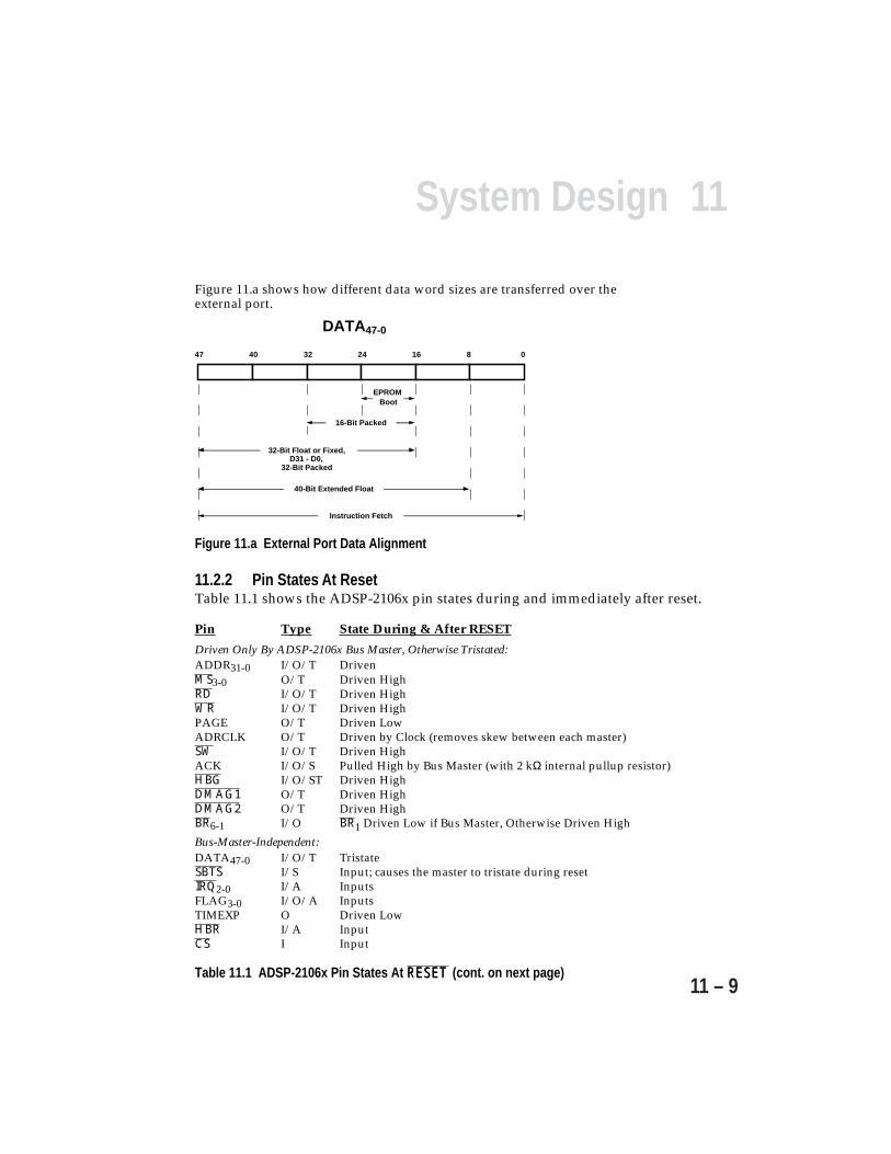
11System Design
11 – 9
Figure 11.a shows how different data word sizes are transferred over theexternal port.
081624324047
DATA47-0
EPROMBoot
16-Bit Packed
32-Bit Float or Fixed,D31 - D0,
32-Bit Packed
40-Bit Extended Float
Instruction Fetch
Figure 11.a External Port Data Alignment
11.2.2 Pin States At ResetTable 11.1 shows the ADSP-2106x pin states during and immediately after reset.
Pin Type State During & After RESET
Driven Only By ADSP-2106x Bus Master, Otherwise Tristated:ADDR31-0 I/O/T DrivenMS3-0 O/T Driven HighRD I/O/T Driven HighWR I/O/T Driven HighPAGE O/T Driven LowADRCLK O/T Driven by Clock (removes skew between each master)SW I/O/T Driven HighACK I/O/S Pulled High by Bus Master (with 2 kΩ internal pullup resistor)HBG I/O/ST Driven HighDMAG1 O/T Driven HighDMAG2 O/T Driven HighBR6-1 I/O BR1 Driven Low if Bus Master, Otherwise Driven High
Bus-Master-Independent:DATA47-0 I/O/T TristateSBTS I/S Input; causes the master to tristate during resetIRQ2-0 I/A InputsFLAG3-0 I/O/A InputsTIMEXP O Driven LowHBR I/A InputCS I Input
Table 11.1 ADSP-2106x Pin States At RESET RESET (cont. on next page)
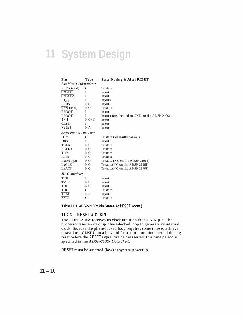
11 System Design
11 – 10
Pin Type State During & After RESETBus-Master-Independent:REDY (o/d) O TristateDMAR1 I InputDMAR2 I InputID2-0 I InputsRPBA I/S InputCPA (o/d) I/O TristateEBOOT I InputLBOOT I Input (must be tied to GND on the ADSP-21061)BMS I/O/T InputCLKIN I InputRESET I/A Input
Serial Ports & Link Ports:DTx O Tristate (for multichannel)DRx I InputTCLKx I/O TristateRCLKx I/O TristateTFSx I/O TristateRFSx I/O TristateLxDAT3-0 I/O Tristate (NC on the ADSP-21061)LxCLK I/O Tristate(NC on the ADSP-21061)LxACK I/O Tristate(NC on the ADSP-21061)
JTAG Interface:TCK I InputTMS I/S InputTDI I/S InputTDO O TristateTRST I/A InputEMU O Tristate
Table 11.1 ADSP-2106x Pin States At RESETRESET (cont.)
11.2.3 RESETRESET & CLKINThe ADSP-2106x receives its clock input on the CLKIN pin. Theprocessor uses an on-chip phase-locked loop to generate its internalclock. Because the phase-locked loop requires some time to achievephase lock, CLKIN must be valid for a minimum time period duringreset before the RESET signal can be deasserted; this time period isspecified in the ADSP-2106x Data Sheet.
RESET must be asserted (low) at system powerup.

11System Design
11 – 11
11.2.3.1 Input Synchronization DelayThe ADSP-2106x has several asynchronous inputs: RESET, TRST, HBR,CS, DMAR1, DMAR2, IRQ2-0, and FLAG3-0 (when configured asinputs). These inputs can be asserted in arbitrary phase to theprocessor clock, CLKIN. The ADSP-2106x synchronizes the inputsprior to recognizing them. The delay associated with recognition iscalled the synchronization delay.
Any asynchronous input must be valid prior to the recognition pointto be recognized in a particular cycle. If an input does not meet thesetup time on a given cycle, it may be recognized in the current cycleor during the next cycle.
Therefore, to ensure recognition of an asynchronous input, it must beasserted for at least one full processor cycle plus setup and hold time(except for RESET, which must be asserted for at least four processorcycles). The minimum time prior to recognition (i.e. the setup and holdtime) is specified in the ADSP-2106x Data Sheet.
11.2.4 Interrupt & Timer PinsThe ADSP-2106x’s external interrupt pins, flag pins, and timer pin canbe used to send and receive control signals to and from other devicesin the system.
Hardware interrupt signals are received on the IRQ2-0 pins. Interruptscan come from devices that require the ADSP-2106x to perform sometask on demand. A memory-mapped peripheral, for example, can usean interrupt to alert the processor that it has data available. Interruptsare described in detail in the Program Sequencing chapter.
The TIMEXP output is generated by the on-chip timer. It indicates toother devices that the programmed time period has expired. The timeris also described in detail in the Program Sequencing chapter.
11.2.5 Flag PinsThe FLAG3-0 pins allow single-bit signalling between the ADSP-2106xand other devices. For example, the ADSP-2106x can raise an outputflag to interrupt a host processor. Each flag pin can be programmed tobe either an input or output. In addition, many ADSP-2106xinstructions can be conditioned on a flag’s input value, enablingefficient communication and synchronization between multipleprocessors or other interfaces.
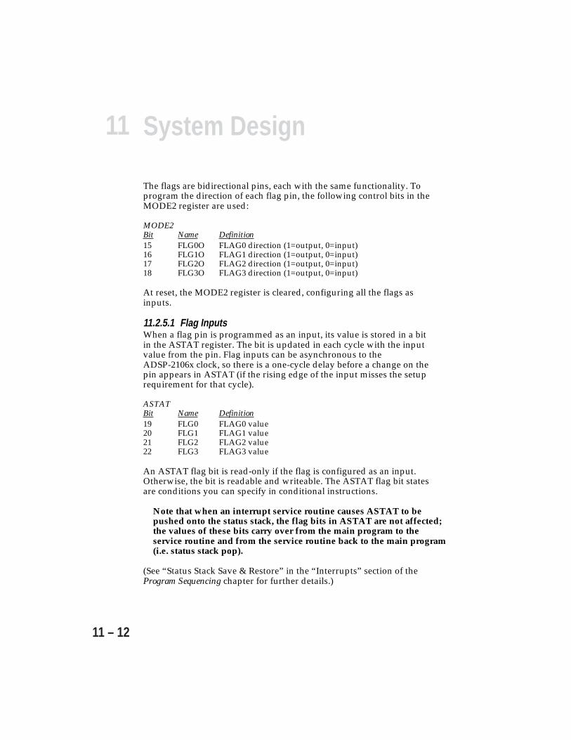
11 System Design
11 – 12
The flags are bidirectional pins, each with the same functionality. Toprogram the direction of each flag pin, the following control bits in theMODE2 register are used:
MODE2Bit Name Definition15 FLG0O FLAG0 direction (1=output, 0=input)16 FLG1O FLAG1 direction (1=output, 0=input)17 FLG2O FLAG2 direction (1=output, 0=input)18 FLG3O FLAG3 direction (1=output, 0=input)
At reset, the MODE2 register is cleared, configuring all the flags asinputs.
11.2.5.1 Flag InputsWhen a flag pin is programmed as an input, its value is stored in a bitin the ASTAT register. The bit is updated in each cycle with the inputvalue from the pin. Flag inputs can be asynchronous to theADSP-2106x clock, so there is a one-cycle delay before a change on thepin appears in ASTAT (if the rising edge of the input misses the setuprequirement for that cycle).
ASTATBit Name Definition19 FLG0 FLAG0 value20 FLG1 FLAG1 value21 FLG2 FLAG2 value22 FLG3 FLAG3 value
An ASTAT flag bit is read-only if the flag is configured as an input.Otherwise, the bit is readable and writeable. The ASTAT flag bit statesare conditions you can specify in conditional instructions.
Note that when an interrupt service routine causes ASTAT to bepushed onto the status stack, the flag bits in ASTAT are not affected;the values of these bits carry over from the main program to theservice routine and from the service routine back to the main program(i.e. status stack pop).
(See “Status Stack Save & Restore” in the “Interrupts” section of theProgram Sequencing chapter for further details.)
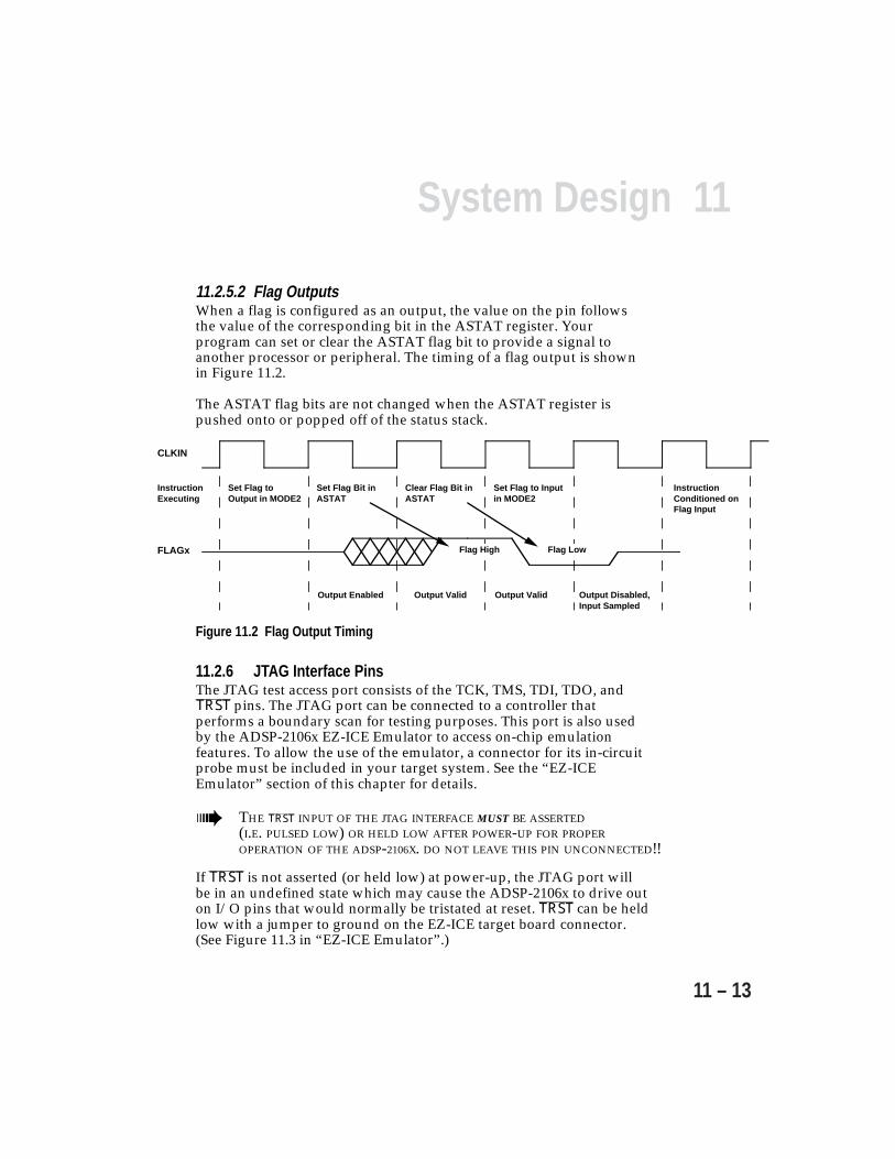
11System Design
11 – 13
11.2.5.2 Flag OutputsWhen a flag is configured as an output, the value on the pin followsthe value of the corresponding bit in the ASTAT register. Yourprogram can set or clear the ASTAT flag bit to provide a signal toanother processor or peripheral. The timing of a flag output is shownin Figure 11.2.
The ASTAT flag bits are not changed when the ASTAT register ispushed onto or popped off of the status stack.
Set Flag to Output in MODE2
Set Flag to Input in MODE2
Output Enabled Output Valid Output Valid Output Disabled, Input Sampled
Set Flag Bit in ASTAT
Clear Flag Bit in ASTAT
CLKIN
FLAGx Flag High Flag Low
Instruction Conditioned on Flag Input
InstructionExecuting
Figure 11.2 Flag Output Timing
11.2.6 JTAG Interface PinsThe JTAG test access port consists of the TCK, TMS, TDI, TDO, andTRST pins. The JTAG port can be connected to a controller thatperforms a boundary scan for testing purposes. This port is also usedby the ADSP-2106x EZ-ICE Emulator to access on-chip emulationfeatures. To allow the use of the emulator, a connector for its in-circuitprobe must be included in your target system. See the “EZ-ICEEmulator” section of this chapter for details.
If TRST is not asserted (or held low) at power-up, the JTAG port willbe in an undefined state which may cause the ADSP-2106x to drive outon I/O pins that would normally be tristated at reset. TRST can be heldlow with a jumper to ground on the EZ-ICE target board connector.(See Figure 11.3 in “EZ-ICE Emulator”.)
THE TRST INPUT OF THE JTAG INTERFACE MUST BE ASSERTED(I.E. PULSED LOW) OR HELD LOW AFTER POWER-UP FOR PROPEROPERATION OF THE ADSP-2106X. DO NOT LEAVE THIS PIN UNCONNECTED!!

11 System Design
11 – 14
11.3 EZ-ICE EMULATORThe ADSP-2106x EZ-ICE Emulator is a development tool fordebugging programs running in real time on your ADSP-2106x targetsystem hardware. The EZ-ICE provides a controlled environment forobserving, debugging, and testing activities in a target system byconnecting directly to the target processor through its JTAG interface.The emulator can monitor system behavior while running at fullspeed. It lets you examine and alter memory locations as well asprocessor registers and stacks.
Because the EZ-ICE controls the target system’s ADSP-2106x throughthe processor’s IEEE 1149.1 JTAG Test Access Port, non-intrusivein-circuit emulation is assured. The emulator does not impact targetloading or timing. The emulator’s in-circuit probe connects to an IBMPC host computer with an ISA bus plug-in board.
Target systems must have a 14-pin connector to accept theEZ-ICE’s in-circuit probe, a 14-pin plug.
11.3.1 Target Board Connector For EZ-ICE ProbeThe ADSP-2106x EZ-ICE Emulator uses the IEEE 1149.1 JTAG testaccess port of the ADSP-2106x to monitor and control the target boardprocessor during emulation. The EZ-ICE probe requires theADSP-2106x’s CLKIN, TMS, TCK, TRST, TDI, TDO, EMU, and GNDsignals be made accessible on the target system via a 14-pin connector(a pin strip header) such as that shown in Figure 11.3. The EZ-ICEprobe plugs directly onto this connector for chip-on-board emulation.You must add this connector to your target board design if you intendto use the ADSP-2106x EZ-ICE. Be sure to allow enough room in yoursystem to fit the EZ-ICE probe onto the 14-pin connector. The length ofthe traces between the connector and the ADSP-2106x’s JTAG pinsshould be as short as possible.
The 14-pin, 2-row pin strip header is keyed at the pin 3 location—youmust remove pin 3 from the header. The pins must be 0.025 inchsquare and at least 0.20 inch in length. Pin spacing should be 0.1 x 0.1inches. The tip of the pins must be at least 0.10 inch higher than thetallest component under the emulator’s probe to allow clearance forthe bottom of the probe. Pin strip headers are available from vendorssuch as 3M, McKenzie, and Samtec.
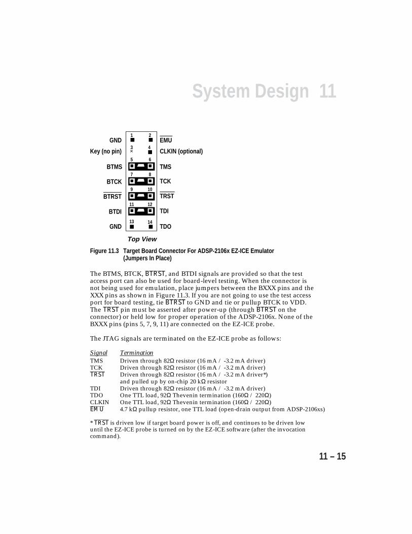
11System Design
11 – 15
CLKIN (optional)
TCK
TDI
TDO
TMS
TRST
BTCK
BTDI
GND
BTMS
BTRST
Key (no pin)
Top View
×
GND EMU1 2
13 14
11 12
9 10
7 8
5 6
3 4
Figure 11.3 Target Board Connector For ADSP-2106x EZ-ICE Emulator(Jumpers In Place)
The BTMS, BTCK, BTRST, and BTDI signals are provided so that the testaccess port can also be used for board-level testing. When the connector isnot being used for emulation, place jumpers between the BXXX pins and theXXX pins as shown in Figure 11.3. If you are not going to use the test accessport for board testing, tie BTRST to GND and tie or pullup BTCK to VDD.The TRST pin must be asserted after power-up (through BTRST on theconnector) or held low for proper operation of the ADSP-2106x. None of theBXXX pins (pins 5, 7, 9, 11) are connected on the EZ-ICE probe.
The JTAG signals are terminated on the EZ-ICE probe as follows:
Signal TerminationTMS Driven through 82Ω resistor (16 mA / -3.2 mA driver)TCK Driven through 82Ω resistor (16 mA / -3.2 mA driver)TRST Driven through 82Ω resistor (16 mA / -3.2 mA driver*)
and pulled up by on-chip 20 kΩ resistorTDI Driven through 82Ω resistor (16 mA / -3.2 mA driver)TDO One TTL load, 92Ω Thevenin termination (160Ω / 220Ω)CLKIN One TTL load, 92Ω Thevenin termination (160Ω / 220Ω)EMU 4.7 kΩ pullup resistor, one TTL load (open-drain output from ADSP-2106xs)
* TRST is driven low if target board power is off, and continues to be driven lowuntil the EZ-ICE probe is turned on by the EZ-ICE software (after the invocationcommand).

11 System Design
11 – 16
Figure 11.4 shows JTAG scan path connections for systems that containmultiple ADSP-2106x processors.
Connecting CLKIN to pin 4 of the EZ-ICE header is optional. The emulatoronly uses CLKIN when performing synchronous multiprocessor operationssuch as starting, stopping, and single-stepping multiple ADSP-2106xs. If youdo not need these operations to occur synchronously on the multipleprocessors, simply tie pin 4 of the EZ-ICE header to ground.
If synchronous multiprocessor operations are needed and CLKIN isconnected, however, clock skew between the multiple ADSP-2106x processorsand the CLKIN pin on the EZ-ICE header must be minimal. If the skew is toolarge, synchronous operations may be off by one cycle between processors.
TCK, TMS, CLKIN (optional), and EMU should be treated as critical signalsin terms of skew, and should be laid out as short as possible on your board. IfTCK, TMS, and CLKIN are driving a large number of ADSP-2106xs (morethan eight) in your system, then treat them as a “clock tree” using multipledrivers. (See “Clock Distribution” in the “High Frequency DesignConsiderations” section of this chapter.) If synchronous multiprocessoroperations are not needed and CLKIN is not connected, just use appropriateparallel termination on TCK and TMS. TDI, TDO, and TRST are not criticalsignals in terms of skew.
ADSP-2106x
#1 JTAGDevice(optional)
ADSP-2106x
#n
EZ-ICE JTAG
Connector
OtherJTAG
Controller
TDI
TCK
TMS
EMU
TRST
TDO
CLKIN
TC
K
TM
S
EM
U
TR
ST
TDI TDO TDI TDO TDI TDO
TC
K
TM
S
EM
U
TR
STTC
K
TM
S
TR
ST
optional
Figure 11.4 JTAG Scan Path Connections For Multiprocessor ADSP-2106x Systems
11System Design
11 – 17
11.4 INPUT SIGNAL CONDITIONINGThe ADSP-2106x SHARC processor is a CMOS device. It has inputconditioning circuits which simplify system design by filtering orlatching input signals to reduce susceptibility to glitches or reflections.The following sections describe why these circuits are needed and theireffect on input signals.
A typical CMOS input consists of an inverter with specific N and Pdevice sizes that cause a switching point of approximately 1.4V. Thislevel is selected to be the midpoint of the standard TTL interfacespecification of VIL=0.8V and VIH=2.0V. This input inverter,unfortunately, has a fast response to input signals and external glitcheswider than about 1 ns. Glitch rejection circuits, filter circuits, andhysteresis are therefore added after the input inverter on someADSP-2106x inputs, as described below.
11.4.1 Glitch Rejection CircuitsThe SHARC processors have on-chip glitch rejection circuits that latchcertain input signals for a fixed time period after a transition has beendetected. The purpose of these circuits is to make the input lesssensitive to reflections and ringing once the first edge has beenreceived. Thus, the circuits will not provide any reduced immunity toglitches that are randomly placed. The glitch rejection circuits are onlyused on some signals that are used as strobes. These signals are:
read and write strobes RD, WRDMA request inputs DMAR1, DMAR2serial port clock inputs RCLK0, RCLK1, TCLK0, RCLK1
The glitch rejection circuit will cause the input signal to be latched forapproximately 4 to 5 ns after a transition has been detected. Glitchrejection circuits are not implemented on the SHARC’s data, address,or control lines that settle out normally before they are used. A glitchrejection circuit is used on the processor’s clock input (CLKIN).
11.4.2 Link Port Input Filter CircuitsThe SHARC’s link port input signals have on-chip filter circuits ratherthan glitch rejection circuits. Filtering is not used on most signals sinceit delays the incoming signal and therefore the timing specifications.Filtering is implemented only on the link port data and clock inputs.This is possible because the link ports are self-synchronized, i.e. theclock and data are sent together. It is not the absolute delay but ratherthe relative delay between clock and data that determines performancemargin.

11 System Design
11 – 18
By filtering both LxCLK and LxDAT3-0 with identical circuits, responseto LxCLK glitches and reflections are reduced but relative delay isunaffected. The filter has the effect of ignoring a full strength pulse (aglitch) narrower than approximately 2 ns. Glitches that are not fullstrength can be somewhat wider. The link ports do not use glitchrejection circuits because they can be used with longer, series-terminated transmission lines where the reflections do not occur nearthe signal transitions.
11.4.3 RESETRESET Input HysteresisHysteresis is used only on the RESET input signal. Hysteresis causesthe switching point of the input inverter to be slightly above 1.4V for arising edge and slightly below 1.4V for a falling edge. The value of thehysteresis is approximately ± 0.1V. The hysteresis is intended toprevent multiple triggering of signals which are allowed to rise slowly,as might be expected on a reset line with a delay implemented by anRC input circuit. Hysteresis is not used to reduce the effect of ringingon SHARC input signals with fast edges, because the amount ofhysteresis that can be used on a CMOS chip is too small to make muchdifference. The small amount of hysteresis allowable is due to therestrictions on the tolerance of the VIL and VIH TTL input levels underworst case conditions. Refer to the ADSP-2106x SHARC Data Sheet forexact specifications.
11.5 HIGH FREQUENCY DESIGN CONSIDERATIONSBecause the ADSP-2106x processor can operate at very fast clockfrequencies, signal integrity and noise problems must be consideredfor circuit board design and layout. The following sections discussthese topics and suggest various techniques to use when designing anddebugging ADSP-2106x systems.
Initial versions of the ADSP-2106x are specified for operation at40 MHz and 33 MHz clocks; the following information is based onthese CLKIN frequencies. Refer to the most up-to-dateADSP-2106x Data Sheet for current clock speed specifications.
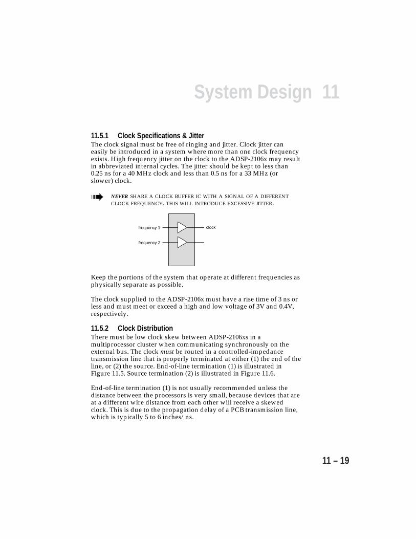
11System Design
11 – 19
11.5.1 Clock Specifications & JitterThe clock signal must be free of ringing and jitter. Clock jitter caneasily be introduced in a system where more than one clock frequencyexists. High frequency jitter on the clock to the ADSP-2106x may resultin abbreviated internal cycles. The jitter should be kept to less than0.25 ns for a 40 MHz clock and less than 0.5 ns for a 33 MHz (orslower) clock.
NEVER SHARE A CLOCK BUFFER IC WITH A SIGNAL OF A DIFFERENTCLOCK FREQUENCY. THIS WILL INTRODUCE EXCESSIVE JITTER.
frequency 1
frequency 2
clock
Keep the portions of the system that operate at different frequencies asphysically separate as possible.
The clock supplied to the ADSP-2106x must have a rise time of 3 ns orless and must meet or exceed a high and low voltage of 3V and 0.4V,respectively.
11.5.2 Clock DistributionThere must be low clock skew between ADSP-2106xs in amultiprocessor cluster when communicating synchronously on theexternal bus. The clock must be routed in a controlled-impedancetransmission line that is properly terminated at either (1) the end of theline, or (2) the source. End-of-line termination (1) is illustrated inFigure 11.5. Source termination (2) is illustrated in Figure 11.6.
End-of-line termination (1) is not usually recommended unless thedistance between the processors is very small, because devices that areat a different wire distance from each other will receive a skewedclock. This is due to the propagation delay of a PCB transmission line,which is typically 5 to 6 inches/ns.
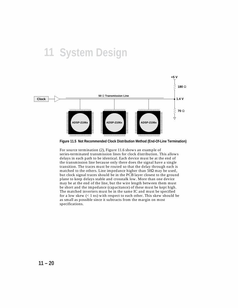
11 System Design
11 – 20
Clock
ADSP-2106x ADSP-2106x ADSP-2106x
1.4 V
70 Ω
180 Ω
+5 V
50 Ω Transmission Line
Figure 11.5 Not Recommended Clock Distribution Method (End-Of-Line Termination)
For source termination (2), Figure 11.6 shows an example ofseries-terminated transmission lines for clock distribution. This allowsdelays in each path to be identical. Each device must be at the end ofthe transmission line because only there does the signal have a singletransition. The traces must be routed so that the delay through each ismatched to the others. Line impedance higher than 50Ω may be used,but clock signal traces should be in the PCB layer closest to the groundplane to keep delays stable and crosstalk low. More than one devicemay be at the end of the line, but the wire length between them mustbe short and the impedance (capacitance) of these must be kept high.The matched inverters must be in the same IC and must be specifiedfor a low skew (< 1 ns) with respect to each other. This skew should beas small as possible since it subtracts from the margin on mostspecifications.

11System Design
11 – 21
Clock
ADSP-2106x
ADSP-2106x
ADSP-2106x
ACTQ240 Octal Inverter(National Semiconductor)
orIDT49FCT805/A
orCY7C992
Buffer Drive Impedance = 10 Ω
A separate buffer and transmission line is needed for each group of processors that are further than 4 inches from each other.
50 Ω Transmission Line40 Ω
50 Ω Transmission Line40 Ω
50 Ω Transmission Line40 Ω
Figure 11.6 Recommended Clock Distribution Method (Source Termination)
11.5.3 Point-To-Point ConnectionsA series termination resistor may be added near the pin for point-to-point connections. This is typically used for link port applicationswhen distances are greater than 6 inches. See Figure 11.7. For morespecific guidence on related issues, see the reference source in theRecommended Reading section for suggestions on transmission linetermination and see the ADSP-2106x Data Sheet for output drivers' riseand fall time data .
For link port operation at a 2X clock rate it is important to maintainlow skew between the data (LxDAT3-0) and clock (LxCLK). For 2Xoperation at CLKIN=40 MHz, a skew of less than 1.25 ns is required.
Although the ADSP-2106x’s serial ports may be operated at a slowrate, the output drivers still have fast edge rates and may requiresource termination for longer distances.
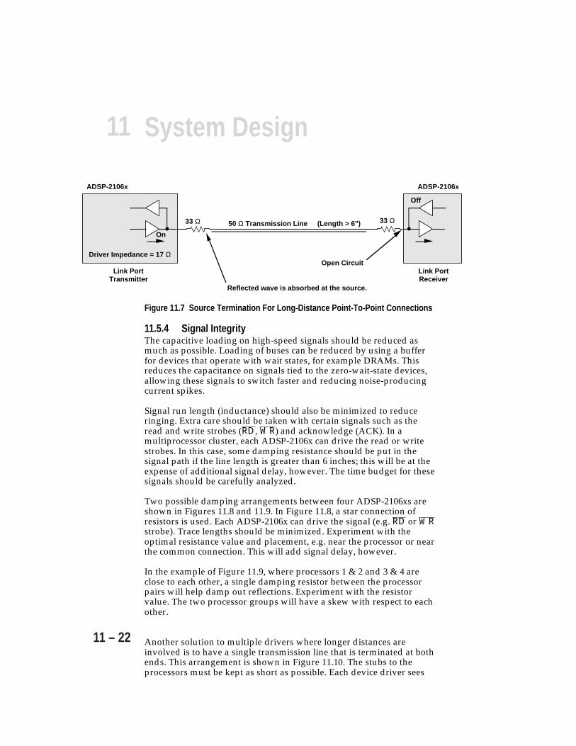
11 System Design
11 – 22
50 Ω Transmission Line (Length > 6")33 Ω
Link PortTransmitter
On
Driver Impedance = 17 Ω
Reflected wave is absorbed at the source.
Link Port Receiver
Off
Open Circuit
33 Ω
ADSP-2106x ADSP-2106x
Figure 11.7 Source Termination For Long-Distance Point-To-Point Connections
11.5.4 Signal IntegrityThe capacitive loading on high-speed signals should be reduced asmuch as possible. Loading of buses can be reduced by using a bufferfor devices that operate with wait states, for example DRAMs. Thisreduces the capacitance on signals tied to the zero-wait-state devices,allowing these signals to switch faster and reducing noise-producingcurrent spikes.
Signal run length (inductance) should also be minimized to reduceringing. Extra care should be taken with certain signals such as theread and write strobes (RD, WR) and acknowledge (ACK). In amultiprocessor cluster, each ADSP-2106x can drive the read or writestrobes. In this case, some damping resistance should be put in thesignal path if the line length is greater than 6 inches; this will be at theexpense of additional signal delay, however. The time budget for thesesignals should be carefully analyzed.
Two possible damping arrangements between four ADSP-2106xs areshown in Figures 11.8 and 11.9. In Figure 11.8, a star connection ofresistors is used. Each ADSP-2106x can drive the signal (e.g. RD or WRstrobe). Trace lengths should be minimized. Experiment with theoptimal resistance value and placement, e.g. near the processor or nearthe common connection. This will add signal delay, however.
In the example of Figure 11.9, where processors 1 & 2 and 3 & 4 areclose to each other, a single damping resistor between the processorpairs will help damp out reflections. Experiment with the resistorvalue. The two processor groups will have a skew with respect to eachother.
Another solution to multiple drivers where longer distances areinvolved is to have a single transmission line that is terminated at bothends. This arrangement is shown in Figure 11.10. The stubs to theprocessors must be kept as short as possible. Each device driver sees
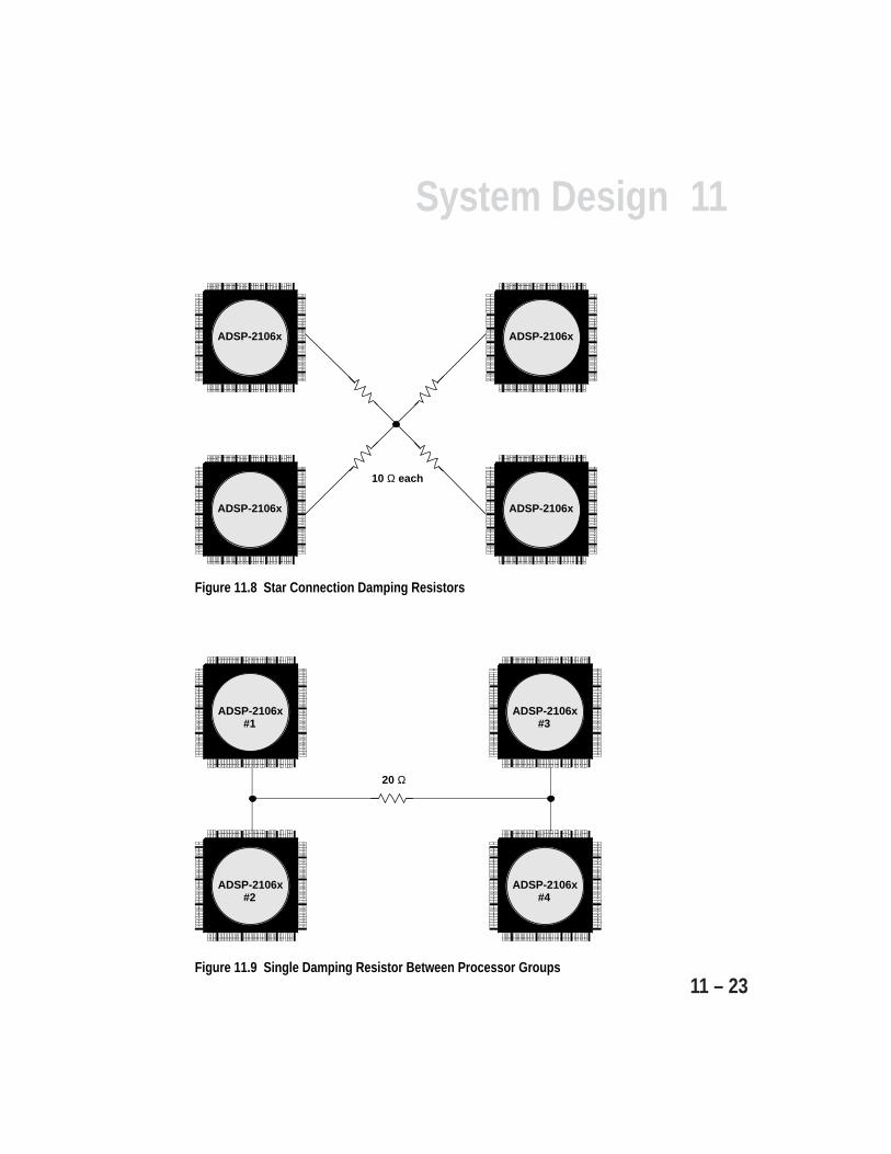
11System Design
11 – 23
ADSP-2106x
ADSP-2106x
ADSP-2106x
ADSP-2106x
10 Ω each
Figure 11.8 Star Connection Damping Resistors
ADSP-2106x#3
ADSP-2106x#4
ADSP-2106x#1
ADSP-2106x#2
20 Ω
Figure 11.9 Single Damping Resistor Between Processor Groups
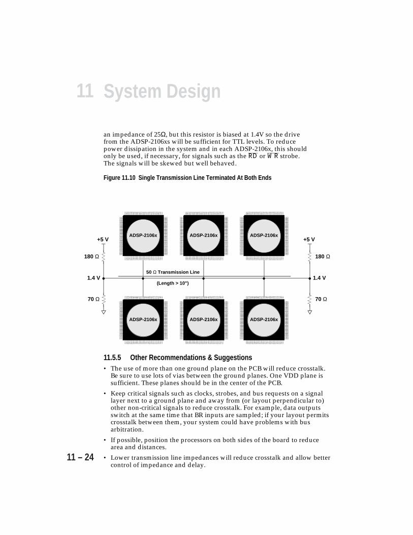
11 System Design
11 – 24
an impedance of 25Ω, but this resistor is biased at 1.4V so the drivefrom the ADSP-2106xs will be sufficient for TTL levels. To reducepower dissipation in the system and in each ADSP-2106x, this shouldonly be used, if necessary, for signals such as the RD or WR strobe.The signals will be skewed but well behaved.
Figure 11.10 Single Transmission Line Terminated At Both Ends
11.5.5 Other Recommendations & Suggestions• The use of more than one ground plane on the PCB will reduce crosstalk.
Be sure to use lots of vias between the ground planes. One VDD plane issufficient. These planes should be in the center of the PCB.
• Keep critical signals such as clocks, strobes, and bus requests on a signallayer next to a ground plane and away from (or layout perpendicular to)other non-critical signals to reduce crosstalk. For example, data outputsswitch at the same time that BR inputs are sampled; if your layout permitscrosstalk between them, your system could have problems with busarbitration.
• If possible, position the processors on both sides of the board to reducearea and distances.
• Lower transmission line impedances will reduce crosstalk and allow bettercontrol of impedance and delay.
ADSP-2106x ADSP-2106x ADSP-2106x
1.4 V
70 Ω
180 Ω
+5 V
50 Ω Transmission Line
(Length > 10")1.4 V
70 Ω
180 Ω
+5 VADSP-2106x ADSP-2106x ADSP-2106x
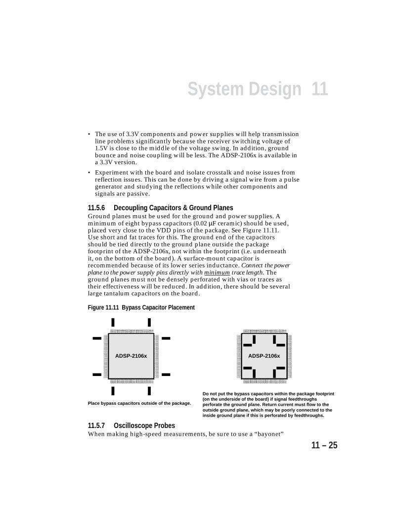
11System Design
11 – 25
• The use of 3.3V components and power supplies will help transmissionline problems significantly because the receiver switching voltage of1.5V is close to the middle of the voltage swing. In addition, groundbounce and noise coupling will be less. The ADSP-2106x is available ina 3.3V version.
• Experiment with the board and isolate crosstalk and noise issues fromreflection issues. This can be done by driving a signal wire from a pulsegenerator and studying the reflections while other components andsignals are passive.
11.5.6 Decoupling Capacitors & Ground PlanesGround planes must be used for the ground and power supplies. Aminimum of eight bypass capacitors (0.02 µF ceramic) should be used,placed very close to the VDD pins of the package. See Figure 11.11.Use short and fat traces for this. The ground end of the capacitorsshould be tied directly to the ground plane outside the packagefootprint of the ADSP-2106x, not within the footprint (i.e. underneathit, on the bottom of the board). A surface-mount capacitor isrecommended because of its lower series inductance. Connect the powerplane to the power supply pins directly with minimum trace length. Theground planes must not be densely perforated with vias or traces astheir effectiveness will be reduced. In addition, there should be severallarge tantalum capacitors on the board.
Figure 11.11 Bypass Capacitor Placement
ADSP-2106x ADSP-2106x
Do not put the bypass capacitors within the package footprint (on the underside of the board) if signal feedthroughs perforate the ground plane. Return current must flow to the outside ground plane, which may be poorly connected to the inside ground plane if this is perforated by feedthroughs.
Place bypass capacitors outside of the package.
11.5.7 Oscilloscope ProbesWhen making high-speed measurements, be sure to use a “bayonet”

11 System Design
11 – 26
type or similarly short (< 0.5 inch) ground clip, attached to the tip ofthe oscilloscope probe. The probe should be a low-capacitance activeprobe with 3 pF or less of loading. The use of a standard ground clipwith 4 inches of ground lead will cause ringing to be seen on thedisplayed trace and will make the signal appear to have excessiveovershoot and undershoot. A 1 GHz or better sampling oscilloscope isneeded to see the signals accurately.
11.5.8 Recommended ReadingHigh-Speed Digital Design: A Handbook of Black Magic is recommendedfor further reading. This book is a technical reference that covers theproblems encountered in state-of-the-art, high-frequency digital circuitdesign, and is an excellent source of information and practical ideas.Topics covered in the book include:
• High-Speed Properties of Logic Gates• Measurement Techniques• Transmission Lines• Ground Planes & Layer Stacking• Terminations• Vias• Power Systems• Connectors• Ribbon Cables• Clock Distribution• Clock Oscillators
High-Speed Digital Design: A Handbook of Black MagicJohnson & GrahamPrentice Hall, Inc.ISBN 0-13-395724-1
11.6 BOOTINGPrograms can be automatically downloaded to the internal memory ofan ADSP-2106x after power-up or after a software reset. This process is
11System Design
11 – 27
called booting.
The ADSP-2106x supports three booting modes: EPROM, host, andlink port. “No boot” mode may also be configured. Each booting modepacks boot data into 48-bit instructions and uses Channel 6 of theADSP-2106x’s on-chip DMA controller to transfer the instructions tointernal memory. For EPROM booting via the external port, theADSP-2106x reads data from an 8-bit external EPROM. For host portbooting, the ADSP-2106x accepts data from a 16-bit hostmicroprocessor (or other external device). For link port booting, theADSP-2106x receives 4-bit wide data in link buffer 4. If no boot mode isselected, the ADSP-2106x starts executing instructions from address0x0040 0004 in external memory.
The primary configuration of DMA Channel 6, used with external portbuffer EPB0, is used for EPROM and host booting. The alternateconfiguration of DMA Channel 6, for link buffer 4, is used for link portbooting. The DMAC6 control register is specially initialized for bootingin each case.
After the boot process loads 256 words into memory locations 0x20000through 0x200FF (using any boot method), the processor beginsexecuting instructions. Because most applications require more than256 words of instructions and initialization data, the 256 wordstypically serve as a loading routine for the application. Analog Devicessupplies a loading routine (Loader Kernel) that can load an entireprogram. This routine comes with the development tools. For moreinformation on the Loader Kernel, see the development toolsdocumentation.
The following sections discuss the different booting modes in detailand describe additional functionality related to booting.
11.6.1 Selecting The Booting ModeThe booting mode is selected using the LBOOT, EBOOT, and BMSpins, as shown in Table 11.2.
EPROM booting is selected when the EBOOT input is high. This causesBMS to become an output, to be used as the boot EPROM chip select.When EBOOT is low, BMS becomes an input used to select between

11 System Design
11 – 28
Pin Type DescriptionEBOOT I EPROM Boot Select. When EBOOT is high, the ADSP-2106x
is configured for booting from an 8-bit EPROM. WhenEBOOT is low, the LBOOT and BMS inputs determinebooting mode. See table below. This signal is a systemconfiguration selection which should be hardwired.
LBOOT I Link Boot – Host Boot Select. When LBOOT is high, theADSP-2106x is configured for link port booting. WhenLBOOT is low, the ADSP-2106x is configured for hostprocessor booting or no booting. See table below. Thissignal is a system configuration selection which should behardwired.
BMS I/O/T* Boot Memory Select. Output: Used as chip select for bootEPROM devices (when EBOOT=1, LBOOT=0). In amultiprocessor system, BMS is output by the bus master.Input: When low, indicates that no booting will occur andthat ADSP-2106x will begin executing instructions fromexternal memory. See table below. This input is a systemconfiguration selection which should be hardwired.
* Tristatable only in EPROM boot mode (when BMS is an output).
Table 11.2 Boot Mode Selection Pins
EBOOT LBOOT BMS Booting Mode1 0 output EPROM (connect BMS to EPROM chip select)0 0 1 (input) Host processor0 1 1 (input) Link port0 0 0 (input) No booting. Processor executes from external memory.0 1 0 (input) reserved1 1 x (input) reserved
11System Design
11 – 29
host boot mode or no boot mode. In EPROM boot mode, BMS isdeasserted when the ADSP-2106x is not the bus master.
Note that when using any of the power-up booting modes, address0x0002 0004 should not contain a valid instruction since it is notexecuted during the booting sequence. A NOP or IDLE instructionshould be placed at this location.
11.6.2 EPROM BootingEPROM booting through the external port is selected when the EBOOTinput is high. The byte-wide boot EPROM must be connected to databus pins 23-16 (DATA23-16). The lowest address pins of theADSP-2106x should be connected to the EPROM’s address lines. TheEPROM’s chip select should be connected to BMS and its outputenable should be connected to RD.
In a multiprocessor system, the BMS output is only driven by theADSP-2106x bus master. This allows wire-ORing of multiple BMSsignals for a single common boot EPROM.
You can boot any number of ADSP-2106x's from a single EPROM,using the same code for each processor or differing code for each.
During reset, the ADSP-2106x’s ACK line is internally pulled high witha 2 kΩ equivalent resistor and is held high with an internal keeperlatch. It is not necessary to use an external pullup resistor on the ACKline during booting or at any other time.
11.6.2.1 Bootstrapping (256 Instructions)When EPROM boot mode is configured, the External Port DMAChannel 6 (DMAC6) becomes active following reset; it is initialized to0x02A1, which allows external port DMA enable and selects DTYPEfor instruction words. The packing mode bits (PMODE) are ignored,and 8-to-48 bit packing is forced with least-significant-word first.
The UBWS and UBWM fields of the WAIT register are initialized togenerate six wait states (seven cycles total) for the EPROM access inunbanked external memory space. (Note that wait states defined forunbanked memory are applied to BMS-asserted accesses.)
The UBWM field's initial value selects internal wait and externalacknowledge. Initially, the SHARC asserts acknowledge (high), but (ifanother device drives acknowledge low during EPROM boot) the
11 System Design
11 – 30
SHARC could latch acknoledge low. The SHARC responds to thedeasserted (low) acknowledge as a hold off from the EPROM, insertingwait states continually and preventing completion of the EPROM boot.To avoid this type of boot holdoff, change the value in the WAITregister, setting the UBWM value to internal wait mode (01) early in the256 word boot process.
Table 11.3 shows how the DMA Channel 6 parameter registers areinitialized at reset for EPROM booting. The count register (C6) isinitialized to 0x0100 for transferring 256 words to internal memory. Theexternal count register (EC6), which is used when external addresses aregenerated by the DMA controller, is initialized to 0x0600 (i.e. 0x0100words with six bytes per word).
Parameter InitializationRegister ValueII6 0x0002 0000IM6 uninitialized (increment by 1 is automatic)C6 0x0100 (256 instruction words)CP6 uninitializedGP6 uninitializedEI6 0x0040 0000EM6 uninitialized (increment by 1 is automatic)EC6 0x0600 (256 words × 6 bytes/word)
Table 11.3 DMA Channel 6 Parameter Register Initialization For EPROM Booting
At system start-up, when the ADSP-2106x’s RESET input goes inactive,the following sequence occurs:
1. The ADSP-2106x goes into an idle state, identical to that caused by theIDLE instruction. The program counter (PC) is set to address0x0002 0004.
2. The DMA parameter registers for channel 6 are initialized (as shownin Table 11.3 above).
3. BMS becomes the boot EPROM chip select.4. 8-bit Master Mode DMA transfers from EPROM to internal memory
begin, on the external port data bus lines 23-16.5. The external address lines (ADDR31-0) start at 0x0040 0000 and
increment after each access.6. The RD strobe asserts as in a normal memory access, with six wait
states (seven cycles).
The ADSP-2106x’s DMA controller reads the 8-bit EPROM words, packsthem into 48-bit instruction words, and transfers them to internalmemory until 256 words have been loaded. The EPROM is automatically
11System Design
11 – 31
selected by the BMS pin; other memory select pins are disabled. The DMAexternal count register (EC6) decrements after each EPROM transfer.When EC6 reaches zero, the following wake-up sequence occurs:
1. The DMA transfers stop.2. The External Port DMA Channel 6 interrupt (EP0I) is activated.3. BMS is deactivated and normal external memory selects are activated.4. The ADSP-2106x vectors to the EP0I interrupt vector at 0x0002 0040.
At this point the ADSP-2106x has completed its booting mode and isexecuting instructions normally. The first instruction at the EP0I interruptvector location, address 0x0002 0040, should be an RTI (Return FromInterrupt). This will return execution to the reset routine at location0x0002 0005 where normal program execution can resume. After this hasoccurred, your program can write a different service routine at the EP0Ivector location 0x0002 0040.
Remember that when using any of the power-up booting modes, location0x0002 0004 should not contain a valid instruction since it is not executedduring the booting sequence. A NOP or IDLE instruction should be placedat this location.
11.6.2.2 Loading The Remaining EPROM DataThe EPROM boot mode only loads 256 instructions during bootstrapping.If your entire application must be loaded into internal memory from theEPROM, the ADSP-2106x must gain access to the boot EPROM afterbootstrapping has completed. The BSO bit in the SYSCON registerprovides this capability.
The BSO bit, when set, overrides the external memory selects and causesthe BMS pin to assert (low) for an external port DMA transfer. Yourbootstrap program should first set the BSO bit in SYSCON and then set upan external port DMA channel to read the rest of the EPROM’s contents.Any of the four external port DMA channels may be used:
Control DataChannel# Register BufferDMA Channel 6 DMAC6 EPB0 (Ext. Port DMA Buffer 0)DMA Channel 7 DMAC7 EPB1 (Ext. Port DMA Buffer 1)DMA Channel 8 DMAC8 EPB2 (Ext. Port DMA Buffer 2)DMA Channel 9 DMAC9 EPB3 (Ext. Port DMA Buffer 3)
When BSO=1, the PMODE packing mode bits in the DMAC6 controlregister are ignored and 8-to-48 bit packing is forced for reads. (Note that8-bit packing is only available during EPROM booting or on DMA reads

11 System Design
11 – 32
when BSO is set.) While one of the external port DMA channels is beingused in conjunction with the BSO bit, none of the other three channels maybe used.
When BSO=1, BMS is not asserted by a core processor access, only by aDMA transfer. This allows your bootstrap program (running on the ADSP-2106x core) to perform other external accesses to non-boot memory.
11.6.2.3 Writing to BMS Memory SpaceYou can also write to ADSP-2106x (SHARC) BMS space using the boot selectoverride (BSO mode). The BSO (Boot Select Override) mode bit in theSYSCON register allows the BMS pin to be asserted under software control.In many systems, the boot data may need to be updated or modified. Inthese cases, the PROM may be substituted by a write-able EEPROM orFLASH memory.
To write to memory with the BMS asserted, use DMA channels 7, 8 or 9, butnot DMA channel 6. With BSO set, DMA channel 6 should only be used forreads. This limitation of accesses appears because DMA channel 6 ishardwired for a special 8-bit boot read mode. When BSO is set, a write withDMA channel 6 with BSO set results in illegal chip operation.
When BSO is set, DMA channels 7-9 can be used with any of the modesavailable in the DMACx register (for read or write), any packing mode, andany data or instruction.
On DMA writes with BSO=1, 16- to 48-bit packing is forced and the PMODEbits are ignored. Because BMS space is 8-bits wide and no 8-bit packingmode is available for these writes, one must use the shifter to place data inthe correct location for each write.
11.6.3 Host BootingBooting the ADSP-2106x from a 16-bit host processor is performed via thedata and address buses of the external port. The ADSP-2106x’s LBOOT pinselects between link port booting and host port booting: LBOOT must below for host booting, with EBOOT low and BMS high. When host booting isconfigured, the ADSP-2106x will enter slave mode after reset and wait forthe host to download the boot program.
After reset the ADSP-2106x goes into an idle state, identical to that causedby the IDLE instruction, with the program counter (PC) set to address0x0002 0004. The parameter registers for External Port DMA Channel 6 areinitialized as shown below in Table 11.4, but no DMA transfers are started.
The DMA Channel 6 Control Register (DMAC6) is initialized to 0x00A1,which allows external port DMA enable and selects DTYPE for instruction
11System Design
11 – 33
words, PMODE for 16-to-48 bit word packing, and least-significant-word first. Because the host processor is accessing the EPB0 externalport buffer, the HPM host packing mode bits of the SYSCON registermust be set to correspond to the external bus width specified by thePMODE bits of the DMAC6 control register. If a different packingmode is desired, the host must write to DMAC6 and SYSCON tochange the PMODE and HPM settings.
Parameter InitializationRegister ValueII6 0x0002 0000IM6 uninitialized (increment by 1 is automatic)C6 0x0100 (256 instruction words)CP6 uninitializedGP6 uninitializedEI6 uninitializedEM6 uninitializedEC6 uninitialized
Table 11.4 Ext. Port DMA Channel 6 Parameter Register Initialization For HostBooting
The host initiates the booting operation by asserting the ADSP-2106x’sHost Bus Request input, HBR. This tells the ADSP-2106x that thedefault 16-bit bus width will be used. The host may also optionallyassert the CS chip select input to allow asynchronous transfers (asdescribed in the Host Interface chapter).
After the host receives the HBG (Host Bus Grant) signal back from theADSP-2106x, it can start downloading instructions by writing directlyto EPB0, the external port DMA buffer 0 (which corresponds to DMAchannel 6), or it can change the reset initialization conditions of theADSP-2106x by writing to any of the IOP control registers. The hostmust use data bus pins 31-16 (DATA31-16).
When 256 instructions have been downloaded, the following wake-upsequence occurs:
1. The DMA transfers stop.2. The External Port DMA Channel 6 interrupt (EP0I) is activated.3. The ADSP-2106x vectors to the EP0I interrupt vector at 0x0002 0040.
The first instruction at the EP0I interrupt vector location, address0x0002 0040, should be an RTI (Return From Interrupt). This RTI will
11 System Design
11 – 34
return execution to the reset routine at location 0x0002 0005 wherenormal program execution can resume. After this 256 word load andRTI have occurred, your program can write a different service routineat the EP0I vector location 0x0002 0040. These 256 instructions mustserve as a loader that loads the rest of your program.
Note that External Port DMA Channel 6 must be used for the initialinstruction download because only this channel has its IMASK bit setto enable a DMA done interrupt. VIRPT vector interrupts are disabledat reset, and must be enabled by your ADSP-2106x program (in theIMASK register).
Note that a master ADSP-2106x may boot a slave ADSP-2106x bywriting to its DMAC6 control register and setting the packing mode(PMODE) to 00. This allows instructions to be downloaded directlywithout packing. The wait state setting of 6 on the slave ADSP-2106xdoes not affect the speed of the download since wait states only affectbus master operation.
11.6.4 Link Port BootingThe ADSP-2106x can also be booted through Link Buffer 4 using DMAChannel 6. A four-bit-wide external device must be used to downloadinstructions after system powerup. The output of an eight-bit-wideEPROM can be converted to nibble data by using a 2-to-1 multiplexeron the output, with the address LSB selecting the high- or low-ordernibble.
The external device must provide a clock signal to the link portassigned to link buffer 4. The clock can be any frequency, up to amaximum of the ADSP-2106x clock frequency. The clock’s fallingedges strobe the data into the link port. The most significant 4-bitnibble of the 48-bit instruction must be downloaded first.
The link port booting operation is similar to the host bootingoperation; the II6 and C6 parameter registers for DMA Channel 6 areinitialized to the same values. The DMA Channel 6 Control Register(DMAC6) is initialized to 0x00A0, which disables external port DMAand selects DTYPE for instruction words. The LCTL and LCOM linkport control registers are overridden during link port booting to allowlink buffer 4 to receive 48-bit data. Form more information on thebooting process, see the Host Booting section.
11System Design
11 – 35
11.6.5 Multiprocessor BootingMultiprocessor systems can be booted from a host processor, fromexternal EPROM, through a link port, or from external memory.
11.6.5.1 Multiprocessor Host BootingTo boot multiple ADSP-2106x processors from a host, eachADSP-2106x must have its EBOOT, LBOOT, and BMS pins configuredfor host booting: EBOOT=0, LBOOT=0, and BMS=1. After systempowerup, each ADSP-2106x will be in the idle state and the BRx busrequest lines will be deasserted. The host must assert the HBR inputand boot each ADSP-2106x by asserting its CS pin and downloadinginstructions as described in “Host Booting” above.
11.6.5.2 Multiprocessor EPROM BootingThere are two methods of booting a multiprocessor system from anEPROM. Processors perform the following steps in these methods:
• Arbitrate for the bus• DMA the 256 word boot stream, after becoming bus master• Release the bus• Execute the loaded instructions
All ADSP-2106xs boot in turn from a single EPROM.The BMS signals from each ADSP-2106x may be wire-ORed together todrive the chip select pin of the EPROM. Each ADSP-2106x can boot inturn, according to its priority. When the last one has finished booting,it must inform the others (which may be in the idle state) that programexecution can begin (if all SHARCs are to begin executing instructionssimultaneously). An example system that uses this processors-take-turns technique appears in Figure 11.12. When multiple SHARCs bootfrom one EPROM, the SHARCs can boot either identical code ordifferent code from the EPROM. If the processors load differing code, ajump table (based on processor ID) can be used to select the code foreach processor.

11 System Design
11 – 36
Figure 11.12 Multiple SHARCs Booting From One EPROM, Processors-Take-Turns
Figure 11.13 Multiple SHARCs Booting From One EPROM, One-Boots-Others
EBOOTLBOOT
ADDR31-0
DATA47-0
RD
ACKBMS
EBOOTLBOOT
ADDR31-0
DATA47-0
RD
ACK
EBOOTLBOOT
ADDR31-0
DATA47-0
RD
ACK
ADDR
DATA
ADDR
ESS
DATA
CONT
ROL
RD
CS
DATA23-16
BMS
BMS
ADSP-2106x(S1, Master)
ADSP-2106x(S2, Slave)
ADSP-2106x(S6, Slave)
EPROM
EBOOTLBOOT
ADDR31-0
DATA47-0
RD
BMS
EBOOT
LBOOT
ADDR31-0
DATA47-0
RD
BMS
EBOOT
LBOOT
ADDR31-0
DATA47-0
RD
BMS
ADDR
DATA
ADDR
ESS
DATA
CONT
ROL
RD
CS
DATA23-16
ADSP-2106x(S1)
ADSP-2106x(S2)
ADSP-2106x(S6)
EPROM
Here, multiple SHARCs boot from the same EPROM. For this configuration, the loader routine uses a jump table to indicate the address of the image that loads into each processor. The processors can load the same image or individual images.
11System Design
11 – 37
One ADSP-2106x is booted, which then boots the others.The EBOOT pin of the ADSP-2106x with ID=1 must be set high forEPROM booting. All other ADSP-2106xs should be configured for hostbooting (EBOOT=0, LBOOT=0, and BMS=1), which leaves them in theidle state at startup and allows the ADSP-2106x with ID=1 to becomebus master and boot itself. Only the BMS pin of ADSP-2106x #1 isconnected to the chip select of the EPROM. When ADSP-2106x #1 hasfinished booting, it can boot the remaining ADSP-2106xs by writing totheir external port DMA buffer 0 (EPB0) via multiprocessor memoryspace. An example system that uses this one-boots-others techniqueappears in Figure 11.13.
11.6.5.3 Multiprocessor Link Port BootingIn systems where multiple ADSP-2106xs are not connected by theparallel external bus, booting can be accomplished from a single sourcethrough the link ports. To simultaneously boot all of the ADSP-2106xs,a parallel common connection should be made to Link Buffer 4 on eachof the processors. If only a daisy chain connection exists between theprocessors’ link ports, then each ADSP-2106x can boot the next one inturn. Link Buffer 4 must always be used for booting.
11.6.5.4 Multiprocessor Booting From External MemoryIf external memory contains a program after reset, then theADSP-2106x with ID=1 should be set up for no boot mode; it will beginexecuting from address 0x0040 0004 in external memory. Whenbooting has completed, the other ADSP-2106xs may be booted byADSP-2106x #1 if they are set up for host booting, or they can beginexecuting out of external memory if they are set up for no boot mode.Multiprocessor bus arbitration will allow this booting to occur in anorderly manner. The bus arbitration sequence after reset is described inthe Multiprocessing chapter of this manual.
11.6.6 “No Boot” ModeThe no boot mode of the ADSP-2106x causes the processor to startfetching and executing instructions at address 0x0040 0004 in externalmemory space. In this mode, all DMA control and parameter registersare set equal to their default initialization values.
11.6.7 Interrupt Vector Table LocationIf the ADSP-2106x is booted from an external source (i.e. EPROM, host,or link port booting), the interrupt vector table will be located ininternal memory. If, however, the ADSP-2106x is not booted, and willexecute from external memory, the vector table must be located in theexternal memory.
11 System Design
11 – 38
The IIVT bit in the SYSCON control register can be used to overridethe booting mode in determining where the interrupt vector table islocated. If the ADSP-2106x is not booted (no boot mode), setting IIVT to1 selects an internal vector table while IIVT=0 selects an external vectortable. If the ADSP-2106x is booted from an external source (any modeother than no boot mode), then IIVT has no effect. The defaultinitialization value of IIVT is zero.
11.7 IMPORTANT PROGRAMMING REMINDERSThis section summarizes information that you should keep in mindwhen writing programs.
11.7.1 Extra Cycle ConditionsAll instructions can execute in a single cycle but may take longer insome cases as described below.
11.7.1.1 Nondelayed BranchesA nondelayed branch instruction (JUMP, CALL, RTS or RTI) fetchesbut does not execute the two instructions that follow it. Instead, theseoperations are aborted and the processor executes two NOPs.
This two-cycle delay can be avoided by using delayed branches, whichexecute the two instructions following the branch instruction. Thetradeoff is that the actual program flow does not match the apparentorder of operations in the program; you must remember that the twoextra instructions are executed before the branch is taken.
11.7.1.2 Program Memory Data Access With Cache MissThe ADSP-2106x checks the instruction cache on every programmemory data access. If the instruction needed is in the cache, theinstruction fetch from the cache happens in parallel with the PM busdata access and the instruction executes in a single cycle. However, ifthe instruction is not in the cache, the ADSP-2106x must wait for thePM bus data access to complete before it can fetch the next instruction.This results in a minimum one-cycle delay, more if the PM bus dataaccess uses external memory with wait states.
This delay will occur even if the PM bus data access is conditional andthe condition is false.
See “Dual Data Accesses” later in this section for additionalinformation.
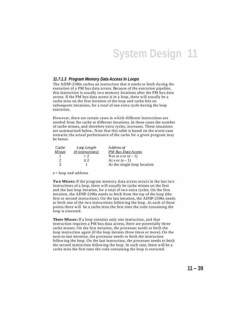
11System Design
11 – 39
11.7.1.3 Program Memory Data Access In LoopsThe ADSP-2106x caches an instruction that it needs to fetch during theexecution of a PM bus data access. Because of the execution pipeline,this instruction is usually two memory locations after the PM bus dataaccess. If the PM bus data access is in a loop, there will usually be acache miss on the first iteration of the loop and cache hits onsubsequent iterations, for a total of one extra cycle during the loopexecution.
However, there are certain cases in which different instructions areneeded from the cache at different iterations. In these cases the numberof cache misses, and therefore extra cycles, increases. These situationsare summarized below. Note that this table is based on the worst-casescenario; the actual performance of the cache for a given program maybe better.
Cache Loop Length Address ofMisses (# instructions) PM Bus Data Access
1 > 2 Not at e or (e – 1)2 ≥ 2 At e or (e – 1)3 1 At the single loop location
e = loop end address
Two Misses: If the program memory data access occurs in the last twoinstructions of a loop, there will usually be cache misses on the firstand the last loop iteration, for a total of two extra cycles. On the firstiteration, the ADSP-2106x needs to fetch from the top of the loop (thefirst or second instruction). On the last iteration, the ADSP-2106x needsto fetch one of the two instructions following the loop. At each of thesepoints there will be a cache miss the first time the code containing theloop is executed.
Three Misses: If a loop contains only one instruction, and thatinstruction requires a PM bus data access, there are potentially threecache misses. On the first iteration, the processor needs to fetch theloop instruction again (if the loop iterates three times or more). On thenext-to-last iteration, the processor needs to fetch the instructionfollowing the loop. On the last instruction, the processor needs to fetchthe second instruction following the loop. In each case, there will be acache miss the first time the code containing the loop is executed.
11 System Design
11 – 40
11.7.1.4 One- & Two-Instruction LoopsCounter-based loops that have only one or two instructions can causedelays if not executed a minimum number of times. The ADSP-2106xchecks the termination condition two cycles before it exits the loop. Inthese short loops, the ADSP-2106x has already looped back when thetermination condition is tested. Thus, if the termination condition teststrue, the two instructions in the pipeline must be aborted and NOPsexecuted instead.
Specifically, a loop of length one executed one or two times or a loop oflength two executed only once incurs two cycles of overhead becausethere are two aborted instructions after the last iteration. Note thatthese overhead cycles are in addition to any extra cycles caused by aPM bus data access inside the loop (see previous section). To avoidoverhead, use straight-line code instead of loops in these cases.
11.7.1.5 DAG Register WritesWhen an instruction that writes to a DAG register is followed by aninstruction that uses any register in the same DAG for data addressing,modify instructions, or indirect jumps, the ADSP-2106x inserts an extra(NOP) cycle between the two instructions. This happens because thesame bus is needed by both operations in the same cycle, therefore thesecond operation must be delayed. An example is:
L2=8;DM(I0,M1)=R1;
Because L2 is in the same DAG as I0 (and M1), an extra cycle isinserted after the write to L2.
11.7.1.6 Wait StatesAn external memory access can be programmed to include a specificnumber of wait states and bus idle cycles, and (or) to wait for anexternal acknowledge signal (ACK) before completing. If onlyinternally programmed wait states and bus idle cycles are used, thedelay is exactly the number of wait states and bus idle cycles(1 waitstate = 1 cycle). If the external acknowledge signal is used,either alone or in combination with programmed wait states, the delaydepends on the external system and can vary.
11.7.2 Delayed Branch RestrictionsA delayed branch instruction and the two instructions that follow itmust be executed sequentially. Any interrupt that occurs between a
11System Design
11 – 41
delayed branch instruction and either of the two instructions thatfollow is not processed until the branch is complete.
Delayed branching can be used with the JUMP, CALL, RTS, and RTIinstructions. For delayed JUMPs, the following instructions may not beused in the two locations immediately after the jump:
• Other JUMP, CALL, RTS, or RTI instructions• DO UNTIL instruction
For a delayed CALL, RTS, or RTI, the following instructions may notbe used in the next two locations:
• Other JUMP, CALL, RTS, or RTI instructions• DO UNTIL instruction• Pushes or Pops of the PC stack• Writes to the PC stack or PC stack pointer
11.7.3 Circular Buffer InitializationYou set up a circular buffer by initializing an L register with a positive,nonzero value and loading the corresponding (same-numbered)B register with the base address of the buffer. (The base address, orstarting address, is the lowest address of the buffer.) Thecorresponding I register is automatically loaded with this samestarting address.
11.7.4 Disallowed DAG Register TransfersThe following instructions execute on the ADSP-2106x, but causeincorrect results. These instructions are disallowed by the assembler:
• An instruction that stores a DAG register in memory using indirectaddressing from the same DAG, with or without update of the indexregister (I). The instruction writes the wrong data to memory orupdates the wrong index register.
DM(M2,I1)=I0; or DM(I1,M2)=I0;
• An instruction that loads a DAG register from memory using indirectaddressing from the same DAG, with update of the index register.The instruction will either load the DAG register or update the indexregister, but not both.
L2=DM(I1,M0);
11 System Design
11 – 42
11.7.5 Two Writes To Register FileIf two writes to the same register file location take place in the samecycle, only the write with higher precedence actually occurs.Precedence is determined by the source of the data being written;from highest to lowest, the precedence is:
• Data memory (DM bus) or universal register• Program memory (PM bus)• ALU• Multiplier• Shifter
11.7.6 Computation UnitsIn fixed-point to floating-point conversion, the rounding boundary isalways 40 bits even if the RND32 bit is set.
The ALU Zero flag (AZ) signifies floating-point underflow as well as azero result.
Transfers between MR registers and the register file are consideredmultiplier operations, and are listed with the multiplier operations inAppendix B, Compute Operation Reference.
11.7.7 Memory Space Access RestrictionsThe ADSP-2106x’s three internal buses, PM, DM, and I/O, can be usedto access the processor’s memory map according to the following rules:
• The DM bus can access all memory spaces.• The PM bus can access only Internal Memory Space and the lowest
12 megawords of External Memory Space.• The I/O bus can access all memory spaces except for the
memory-mapped IOP registers (in Internal Memory Space).
Note that in silicon revision 1.0 and earlier, pre-modify addressingoperations must not change the memory space of the address; forexample, pre-modification of an address in Internal Memory Space shouldnot generate an address in External Memory Space. The one exception tothis rule is: an indirect JUMP or CALL instruction with pre-modifyaddressing can jump from internal memory to external memory. Siliconrevisions 2.x and later do not have this pre-modify limitation.
11System Design
11 – 43
11.7.8 Mixing 32-Bit & 48-Bit Words In A Memory Block32-bit data words and 48-bit instruction words can be stored in thesame memory block, with the restriction that all instructions must resideat addresses lower than the data. No instruction may be stored at anaddress higher than the lowest address of any data word. Thisrestriction is necessary to prevent addresses for 32-bit words and 48-bitwords from overlapping. Instruction storage must start at the lowestaddress in the block.
11.7.9 16-Bit Short Words16-bit short words read into ADSP-2106x registers are automaticallyextended into 32-bit integers. The upper 16 bits can be zero-filled orsign-extended, as determined by the value of the SSE bit in the MODE1register. If SSE=0, the upper 16 bits are zero-filled. If SSE=1, the upper16 bits are sign-extended (except when reading a short word into thePX register, which is always zero-filled).
11.7.10 Dual Data AccessesThe ADSP-2106x’s PM and DM buses allow the processor core tosimultaneously access instructions and data from both memory blocks.Instructions are fetched over the PM bus or from the instruction cache.Data can be accessed over both the DM bus (using DAG1) and thePM bus (using DAG2).
The ADSP-2106x’s two memory blocks can be configured to storedifferent combinations of 48-bit instruction words and 32-bit datawords. Maximum efficiency (i.e. single-cycle execution of dual-data-access instructions), though, is achieved when one block contains a mixof instructions and PM bus data while the other block contains DM busdata only. This means that for an instruction requiring two dataaccesses, the PM bus (and DAG2) is used to access data from the mixedblock, the DM bus (and DAG1) is used to access data from thedata-only block, and the instruction must be available from the cache.Another way to partition the data is to store one operand in externalmemory and the other in either block of internal memory.
In typical DSP applications such as digital filters and FFTs, two dataoperands must be accessed for some instructions. In a digital filter, forexample, the filter coefficients can be stored in 32-bit words in thesame memory block that contains the 48-bit instructions, while 32-bitdata samples are stored in the other block. This provides single-cycleexecution of dual-data-access instructions, with the filter coefficientsbeing accessed by DAG2 over the PM bus and the instruction availablefrom the cache.

11 System Design
11 – 44
To assure single-cycle, parallel accesses of two on-chip memorylocations, the following conditions must be met:
• The two addresses must be located in different memory blocks(i.e. one in Block 0, one in Block 1).
• One address must be generated by DAG1 and the other by DAG2.• The DAG1 address must not point to the same memory block that
instructions are being fetched from.• The instruction should be of the form:compute, Rx=DM(I0-I7,M0-M7), Ry=PM(I8-I15,M8-M15);
(Note that reads and writes may be intermixed.)
11.8 DATA DELAYS, LATENCIES, & THROUGHPUTTables 11.5 and 11.6 specify data delays, latencies, and throughput forthe ADSP-2106x. Data delay and latency are defined as the number ofcycles (after the first cycle) required to complete the operation. Thus azero-wait-state memory has a data delay of zero, and a single-wait-state memory has a data delay of one. Throughput is the maximum rateat which the operation is performed.
Data delay and throughput are the same whether the access is from ahost processor or from another ADSP-2106x.
11.9 EXECUTION STALLSThe following events can cause execution stalls in the ADSP-2106xcore.
Program Sequencer Stalls• 1 cycle on a program memory data access with instruction cache miss• 2 cycles on non-delayed branches• 2 cycles on normal interrupts• 5 cycles on vector interrupt (VIRPT)• 1-2 cycles on short loops w/small iterations• n cycles on IDLE instruction
DAG Stalls• 1 cycle hold on register conflict
11System Design
11 – 45
Memory Stalls• 1 cycle on PM and DM bus accesses to the same block of internal
memory• n cycles if conflicting accesses to external memory (PM and DM bus
accesses must complete)• n cycles if access to external memory (until I/O buffers are cleared out)• n cycles if external access and ADSP-2106x does not own external bus• n cycles until external access is complete (i.e. waitstates, idle cycles, etc.)
IOP Register Stalls• n cycles if PM and DM bus access to IOP registers (both must complete)• n cycles if conflict with slave access
DMA Stalls• 1 cycle if an access to a DMA parameter register conflicts with the DMA
address generation (i.e. writing to the register while a register update istaking place or reading while a DMA register read is taking place)
• 1 cycle if an access to a DMA parameter register conflicts with DMAchaining
• n cycles if writing (reading) to a DMA buffer and the buffer is full(empty)
Link Port & Serial Port Stalls• 1 cycle if two link buffer reads back-to-back• n cycles if write to a full buffer or read from an empty buffer
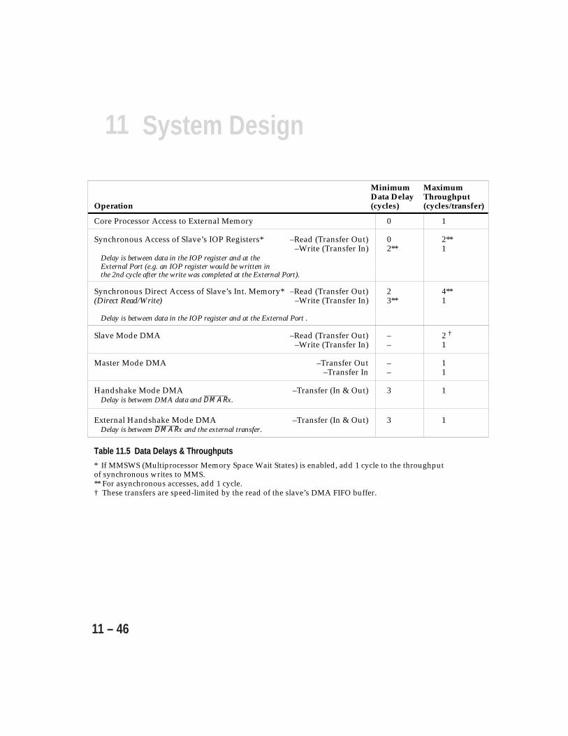
11 System Design
11 – 46
Minimum MaximumData Delay Throughput
Operation (cycles) (cycles/transfer)
Core Processor Access to External Memory 0 1
Synchronous Access of Slave’s IOP Registers* –Read (Transfer Out) 0 2**–Write (Transfer In) 2** 1
Delay is between data in the IOP register and at theExternal Port (e.g. an IOP register would be written inthe 2nd cycle after the write was completed at the External Port).
Synchronous Direct Access of Slave’s Int. Memory* –Read (Transfer Out) 2 4**(Direct Read/Write) –Write (Transfer In) 3** 1
Delay is between data in the IOP register and at the External Port .
Slave Mode DMA –Read (Transfer Out) – 2 †–Write (Transfer In) – 1
Master Mode DMA –Transfer Out – 1–Transfer In – 1
Handshake Mode DMA –Transfer (In & Out) 3 1Delay is between DMA data and DMARx.
External Handshake Mode DMA –Transfer (In & Out) 3 1Delay is between DMARx and the external transfer.
Table 11.5 Data Delays & Throughputs
* If MMSWS (Multiprocessor Memory Space Wait States) is enabled, add 1 cycle to the throughputof synchronous writes to MMS.** For asynchronous accesses, add 1 cycle.† These transfers are speed-limited by the read of the slave’s DMA FIFO buffer.
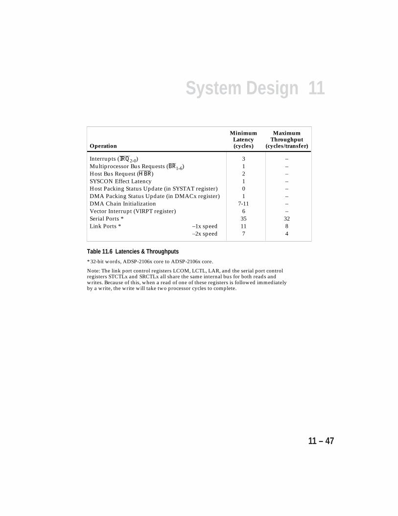
11System Design
11 – 47
Minimum MaximumLatency Throughput
Operation (cycles) (cycles/transfer)
Interrupts (IRQ2-0) 3 –Multiprocessor Bus Requests (BR1-6) 1 –Host Bus Request (HBR) 2 –SYSCON Effect Latency 1 –Host Packing Status Update (in SYSTAT register) 0 –DMA Packing Status Update (in DMACx register) 1 –DMA Chain Initialization 7-11 –Vector Interrupt (VIRPT register) 6 –Serial Ports * 35 32Link Ports * –1x speed 11 8
–2x speed 7 4
Table 11.6 Latencies & Throughputs
* 32-bit words, ADSP-2106x core to ADSP-2106x core.
Note: The link port control registers LCOM, LCTL, LAR, and the serial port controlregisters STCTLx and SRCTLx all share the same internal bus for both reads andwrites. Because of this, when a read of one of these registers is followed immediatelyby a write, the write will take two processor cycles to complete.

11 System Design
11 – 48
AInstruction Set Reference
A – 1
A.1 OVERVIEWThis appendix and the next one describe the ADSP-2106x instruction set indetail. This appendix explains each instruction type, including theassembly language syntax and the opcode that the instruction assemblesto. Many instruction types contain a field for specifying a computeoperation (an operation that uses the ALU, multiplier or shifter). Becausethere are a large number of options available for this field, they aredescribed separately in Appendix B. (Note that data moves between theMR registers and the register file are considered multiplier operations.)
Each instruction is specified in this section. The specification shows thesyntax of the instruction, describes its function, gives one or twoassembly-language examples, and specifies and describes the variousfields of its opcode. The instructions are grouped into four categories:
I. Compute and Move or Modify instructions, which specify a computeoperation in parallel with one or two data moves or an index registermodify.
II. Program Flow Control instructions, which specify various types ofbranches, calls, returns and loops. Some of these instructions may alsospecify a compute operation and/or a data move.
III. Immediate Data Move instructions, which use immediate instructionfields as operands, or use immediate instruction fields for addressing.
IV. Miscellaneous instructions, such as bit modify and test, no operationand idle.
The instructions are numbered from 1 to 23. Some instructions have morethan one syntactical form; for example, Instruction Type 4 has four distinctforms. The instruction number has no bearing on programming, butcorresponds to the opcode recognized by the ADSP-2106x device.
Many instructions can be conditional. These instructions are prefaced byan “IF” plus a condition mnemonic. In a conditional instruction, theexecution of the entire instruction is based on the specified condition.

Instruction Set ReferenceA
A – 2
A.2 INSTRUCTION SET SUMMARYThe next few pages summarize the ADSP-2106x instruction set. Thecompute operations used within each instruction are specified inAppendix B.
(pg. A-16)
(pg. A-17)
(pg. A-18)
(pg. A-20)
(pg. A-22)
(pg. A-24)
(pg. A-26)
Compute & Move or Modify Instructions1. compute, DM(Ia,Mb) = dreg1 , PM(Ic,Md) = dreg2 ;
dreg1 = DM(Ia,Mb) dreg2 = PM(Ic,Md)
2. IF condition compute;
3a. IF condition compute, DM(Ia,Mb) = ureg ;PM(Ic,Md)
3b. IF condition compute, DM(Mb,Ia) = ureg ;PM(Md,Ic)
3c. IF condition compute, ureg = DM(Ia,Mb) ;PM(Ic,Md)
3d. IF condition compute, ureg = DM(Mb,Ia) ;PM(Md,Ic)
4a. IF condition compute, DM(Ia,<data6>) = dreg ;PM(Ic,<data6>)
4b. IF condition compute, DM(<data6>,Ia) = dreg ;PM(<data6>,Ic)
4c. IF condition compute, dreg = DM(Ia,<data6>) ;PM(Ic,<data6>)
4d. IF condition compute, dreg = DM(<data6>,Ia) ;PM(<data6>,Ic)
5. IF condition compute, ureg1 = ureg2 ;
6a. IF condition shiftimm, DM(Ia,Mb) = dreg ;PM(Ic,Md)
6b. IF condition shiftimm, dreg = DM(Ia,Mb) ;PM(Ic,Md)
7. IF condition compute, MODIFY (Ia,Mb) ;(Ic,Md)
Items in italics are an optional part of the instruction.

AInstruction Set Reference
A – 3
Program Flow Control Instructions8. IF condition JUMP <addr24> (DB) ;
(PC, <reladdr24>) (LA)(CI)(DB,LA)(DB,CI)
IF condition CALL <addr24> (DB) ;(PC, <reladdr24>)
9. IF condition JUMP (Md,Ic) (DB) , compute ;(PC, <reladdr6>) (LA) ELSE compute
(CI)(DB,LA)(DB,CI)
IF condition CALL (Md,Ic) (DB) , compute ;(PC, <reladdr6>) ELSE compute
10. IF condition JUMP (Md,Ic) , ELSE compute , DM(Ia,Mb) = dreg ;(PC, <reladdr6>) compute , dreg = DM(Ia,Mb)
11. IF condition RTS (DB) , compute ;(LR) ELSE compute(DB,LR)
IF condition RTI (DB) , compute ;ELSE compute
12. LCNTR = <data16> , DO <addr24> UNTIL LCE ; ureg (PC, <reladdr24>)
13. DO <addr24> UNTIL termination ;(PC, <reladdr24>)
(pg. A-28)
(pg. A-30)
(pg. A-32)
(pg. A-34)
(pg. A-36)
(pg. A-38)
Items in italics are an optional part of the instruction.
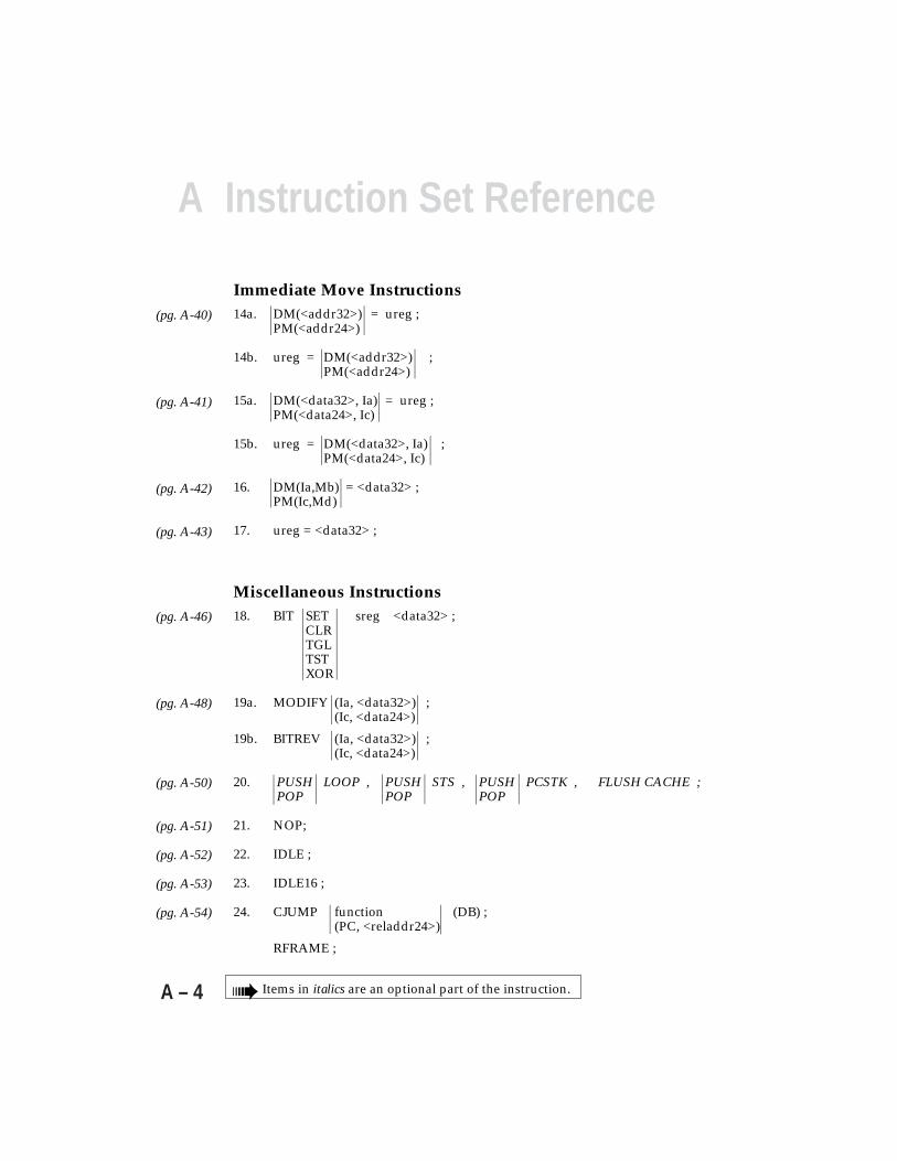
Instruction Set ReferenceA
A – 4
(pg. A-46)
(pg. A-48)
(pg. A-50)
(pg. A-51)
(pg. A-52)
(pg. A-53)
(pg. A-54)
Immediate Move Instructions14a. DM(<addr32>) = ureg ;
PM(<addr24>)
14b. ureg = DM(<addr32>) ;PM(<addr24>)
15a. DM(<data32>, Ia) = ureg ;PM(<data24>, Ic)
15b. ureg = DM(<data32>, Ia) ;PM(<data24>, Ic)
16. DM(Ia,Mb) = <data32> ;PM(Ic,Md)
17. ureg = <data32> ;
(pg. A-40)
(pg. A-41)
(pg. A-42)
(pg. A-43)
Miscellaneous Instructions18. BIT SET sreg <data32> ;
CLRTGLTSTXOR
19a. MODIFY (Ia, <data32>) ;(Ic, <data24>)
19b. BITREV (Ia, <data32>) ;(Ic, <data24>)
20. PUSH LOOP , PUSH STS , PUSH PCSTK , FLUSH CACHE ;POP POP POP
21. NOP;
22. IDLE ;
23. IDLE16 ;
24. CJUMP function (DB) ;(PC, <reladdr24>)
RFRAME ;
Items in italics are an optional part of the instruction.
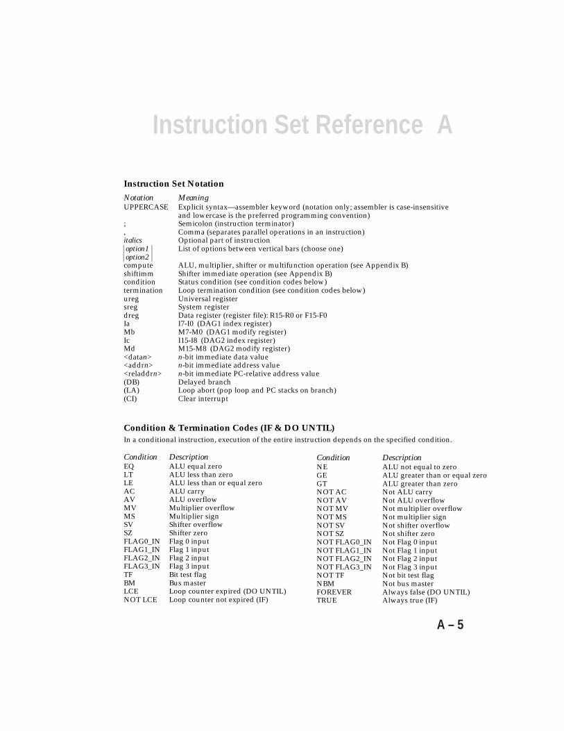
AInstruction Set Reference
A – 5
Instruction Set Notation
Notation MeaningUPPERCASE Explicit syntax—assembler keyword (notation only; assembler is case-insensitive
and lowercase is the preferred programming convention); Semicolon (instruction terminator), Comma (separates parallel operations in an instruction)italics Optional part of instruction option1 List of options between vertical bars (choose one) option2compute ALU, multiplier, shifter or multifunction operation (see Appendix B)shiftimm Shifter immediate operation (see Appendix B)condition Status condition (see condition codes below)termination Loop termination condition (see condition codes below)ureg Universal registersreg System registerdreg Data register (register file): R15-R0 or F15-F0Ia I7-I0 (DAG1 index register)Mb M7-M0 (DAG1 modify register)Ic I15-I8 (DAG2 index register)Md M15-M8 (DAG2 modify register)<datan> n-bit immediate data value<addrn> n-bit immediate address value<reladdrn> n-bit immediate PC-relative address value(DB) Delayed branch(LA) Loop abort (pop loop and PC stacks on branch)(CI) Clear interrupt
Condition & Termination Codes (IF & DO UNTIL)In a conditional instruction, execution of the entire instruction depends on the specified condition.
Condition DescriptionEQ ALU equal zeroLT ALU less than zeroLE ALU less than or equal zeroAC ALU carryAV ALU overflowMV Multiplier overflowMS Multiplier signSV Shifter overflowSZ Shifter zeroFLAG0_IN Flag 0 inputFLAG1_IN Flag 1 inputFLAG2_IN Flag 2 inputFLAG3_IN Flag 3 inputTF Bit test flagBM Bus masterLCE Loop counter expired (DO UNTIL)NOT LCE Loop counter not expired (IF)
Condition DescriptionNE ALU not equal to zeroGE ALU greater than or equal zeroGT ALU greater than zeroNOT AC Not ALU carryNOT AV Not ALU overflowNOT MV Not multiplier overflowNOT MS Not multiplier signNOT SV Not shifter overflowNOT SZ Not shifter zeroNOT FLAG0_IN Not Flag 0 inputNOT FLAG1_IN Not Flag 1 inputNOT FLAG2_IN Not Flag 2 inputNOT FLAG3_IN Not Flag 3 inputNOT TF Not bit test flagNBM Not bus masterFOREVER Always false (DO UNTIL)TRUE Always true (IF)

Instruction Set ReferenceA
A – 6
Universal RegistersRegister FunctionData Register FileR15 - R0 Register file locations, fixed-pointF15 - F0 Register file locations, floating-point
Program SequencerPC Program counter (read-only)PCSTK Top of PC stackPCSTKP PC stack pointerFADDR Fetch address (read-only)DADDR Decode address (read-only)LADDR Loop termination address, code; top of loop address stackCURLCNTR Current loop counter; top of loop count stackLCNTR Loop count for next nested counter-controlled loop
Data Address GeneratorsI7 - I0 DAG1 index registersM7 - M0 DAG1 modify registersL7 - L0 DAG1 length registersB7 - B0 DAG1 base registersI15 - I8 DAG2 index registersM15 - M8 DAG2 modify registersL15 - L8 DAG2 length registersB15 - B8 DAG2 base registers
Bus ExchangePX1 PMD-DMD bus exchange 1 (16 bits)PX2 PMD-DMD bus exchange 2 (32 bits)PX 48-bit combination of PX1 and PX2
TimerTPERIOD Timer periodTCOUNT Timer counter
System RegistersMODE1 Mode control & statusMODE2 Mode control & statusIRPTL Interrupt latchIMASK Interrupt maskIMASKP Interrupt mask pointer (for nesting)ASTAT Arithmetic status flags, bit test flag, etc.STKY Sticky arithmetic status flags, stack status flags, etc.USTAT1 User status register 1USTAT2 User status register 2

AInstruction Set Reference
A – 7
Memory Addressing in Instructions
Direct:
AbsoluteInstruction Types 8, 12, 13, 14Examples: dm(0x000015F0) = astat;
if ne jump label2; 'label2' is an address label
PC-relativeInstruction Types 8, 9, 10, 12, 13Examples: call(pc,10), r0=r6+r3;
do(pc,length) until sz; 'length' is a variable
Register Indirect (using DAG registers):
Post-modify with M register, update I registerInstruction Types 1, 3, 6, 16Examples: f5=pm(i9,m12);
dm(i0,m3)=r3, r1=pm(i15,m10);
Pre-modify with M register, no updateInstruction Types 3, 9, 10Examples: r1=pm(m10,i15);
jump(m13,i11);
Post-modify with immediate value, update I registerInstruction Type 4Examples: f15=dm(i0,6);
if av r1=pm(i15,0x11);
Pre-modify with immediate value, no updateInstruction Types 4, 15Examples: if av r1=pm(0x11,i15);
dm(127,i5)=laddr;
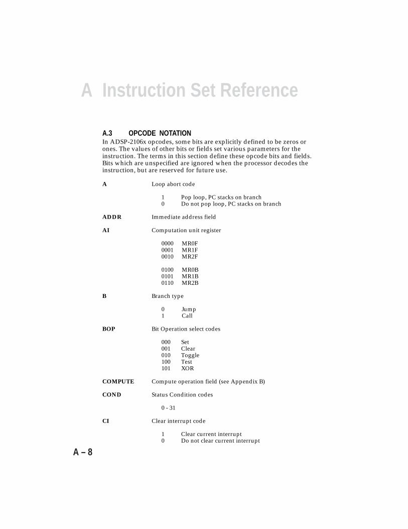
Instruction Set ReferenceA
A – 8
A.3 OPCODE NOTATIONIn ADSP-2106x opcodes, some bits are explicitly defined to be zeros orones. The values of other bits or fields set various parameters for theinstruction. The terms in this section define these opcode bits and fields.Bits which are unspecified are ignored when the processor decodes theinstruction, but are reserved for future use.
A Loop abort code
1 Pop loop, PC stacks on branch0 Do not pop loop, PC stacks on branch
ADDR Immediate address field
AI Computation unit register
0000 MR0F0001 MR1F0010 MR2F
0100 MR0B0101 MR1B0110 MR2B
B Branch type
0 Jump1 Call
BOP Bit Operation select codes
000 Set001 Clear010 Toggle100 Test101 XOR
COMPUTE Compute operation field (see Appendix B)
COND Status Condition codes
0 - 31
CI Clear interrupt code
1 Clear current interrupt0 Do not clear current interrupt

AInstruction Set Reference
A – 9
CU Computation unit select codes
00 ALU01 Multiplier10 Shifter
DATA Immediate data field
DEC Counter decrement code
0 No counter decrement1 Counter decrement
DMD Memory access direction
0 Read1 Write
DMI Index (I) register numbers, DAG1
0 - 7
DMM Modify (M) register numbers, DAG1
0 - 7
DREG Register file locations
0 - 15
E ELSE clause code
0 No ELSE clause1 ELSE clause
FC Flush cache code
0 No cache flush1 Cache flush
G DAG/Memory select
0 DAG1 or Data Memory1 DAG2 or Program Memory
INC Counter increment code
0 No counter increment1 Counter increment
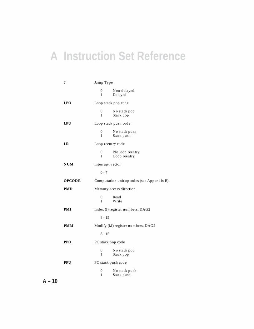
Instruction Set ReferenceA
A – 10
J Jump Type
0 Non-delayed1 Delayed
LPO Loop stack pop code
0 No stack pop1 Stack pop
LPU Loop stack push code
0 No stack push1 Stack push
LR Loop reentry code
0 No loop reentry1 Loop reentry
NUM Interrupt vector
0 - 7
OPCODE Computation unit opcodes (see Appendix B)
PMD Memory access direction
0 Read1 Write
PMI Index (I) register numbers, DAG2
8 - 15
PMM Modify (M) register numbers, DAG2
8 - 15
PPO PC stack pop code
0 No stack pop1 Stack pop
PPU PC stack push code
0 No stack push1 Stack push

AInstruction Set Reference
A – 11
RELADDR PC-relative address field
SPO Status stack pop code
0 No stack pop1 Stack pop
SPU Status stack push code
0 No stack push1 Stack push
SREG System Register code
0 - 15 (see “Universal Register Codes” on the next page)
TERM Termination Condition codes
0 - 31
U Update, index (I) register
0 Pre-modify, no update1 Post-modify with update
UREG Universal Register code
0 - 256 (see “Universal Register Codes” on the next page)
RA, RM, RN, Register file locations for compute operands and resultsRS, RX, RY
0 - 15
RXA ALU x-operand register file location for multifunction operations
8 - 11
RXM Multiplier x-operand register file location for multifunction operations
0 - 3
RYA ALU y-operand register file location for multifunction operations
12 - 15
RYM Multiplier y-operand register file location for multifunction operations
4 - 7

Instruction Set ReferenceA
A – 12
A.4 UNIVERSAL REGISTER CODES
Map 1 Registers:PC program counterPCSTK top of PC stackPCSTKP PC stack pointerFADDR fetch addressDADDR decode addressLADDR loop termination addressCURLCNTR current loop counterLCNTR loop counterR15 - R0 register file locationsI15 - I0 DAG1 and DAG2 index registersM15 - M0 DAG1 and DAG2 modify registersL15 - L0 DAG1 and DAG2 length registersB15 - B0 DAG1 and DAG2 base registers
System Registers:MODE1 mode control 1MODE2 mode control 2IRPTL interrupt latchIMASK interrupt maskIMASKP interrupt mask pointerASTAT arithmetic statusSTKY sticky statusUSTAT1 user status reg 1USTAT2 user status reg 2
Figure A.1 Map 1 Universal Register Codes
0 0 0 0
0 0 0 1
0 0 1 0
0 0 1 1
0 1 0 0
0 1 0 1
0 1 1 0
0 1 1 1
1 0 0 0
1 0 0 1
1 0 1 0
1 0 1 1
1 1 0 0
1 1 0 1
1 1 1 0
1 1 1 1
0 0 0 0 0 0 0 1 0 0 1 0 0 0 1 1
R0
R1
R2
R3
R4
R5
R6
R7
R8
R9
R10
R11
R12
R13
R14
R15
I0
I1
I2
I3
I4
I5
I6
I7
0 1 0 0
L0
L1
L2
L3
L4
L5
L6
L7
0 1 0 1
ASTAT
MODE2
b3 b2 b1 b0
b7 b6 b5 b4
0 1 1 0
STKY
0 1 1 1
CURLCNTR
MODE1
IRPTL
IMASK
PCSTK
PC
(b7=0)
I8
I9
I10
I11
I12
I13
I14
I15
M0
M1
M2
M3
M4
M5
M6
M8
M9
M10
M11
M12
M13
M14
L8
L9
L10
B5
B6
B7
B8
B9
B10
B11L11
L12
L13
L14
B12
B13
B14
B15
B0
B1
B2
B3
B4
LADDR
L15
PCSTKP
M7
M15
SystemRegisters
USTAT1
USTAT2
LCNTR
IMASKP
FADDR
DADDR
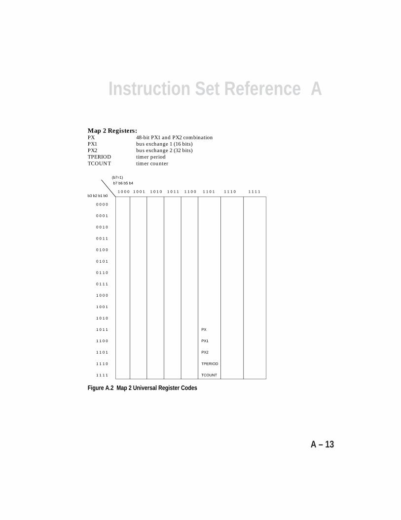
AInstruction Set Reference
A – 13
Map 2 Registers:PX 48-bit PX1 and PX2 combinationPX1 bus exchange 1 (16 bits)PX2 bus exchange 2 (32 bits)TPERIOD timer periodTCOUNT timer counter
Figure A.2 Map 2 Universal Register Codes
0 0 0 0
0 0 0 1
0 0 1 0
0 0 1 1
0 1 0 0
0 1 0 1
0 1 1 0
0 1 1 1
1 0 0 0
1 0 0 1
1 0 1 0
1 0 1 1
1 1 0 0
1 1 0 1
1 1 1 0
1 1 1 1
1 0 0 0 1 0 0 1 1 0 1 0 1 0 1 1 1 1 0 0 1 1 0 1b3 b2 b1 b0
b7 b6 b5 b4
1 1 1 0 1 1 1 1
(b7=1)
TCOUNT
TPERIOD
PX
PX1
PX2

Instruction Set ReferenceA
A – 14
AInstruction Set Reference
A – 15
Group I.Compute and Move Instructions1. Parallel data memory and program memory transfers with register file, optional
compute operation ....................................................................................................A-16
2. Compute operation, optional condition .....................................................................A-17
3. Transfer between data or program memory and universal register, optionalcondition, optional compute operation ......................................................................A-18
4. PC-relative transfer between data or program memory and register file,optional condition, optional compute operation ........................................................A-20
5. Transfer between two universal registers, optional condition, optional computeoperation...................................................................................................................A-22
6. Immediate shift operation, optional condition, optional transfer between data orprogram memory and register file .............................................................................A-24
7. Index register modify, optional condition, optional compute operation .....................A-26
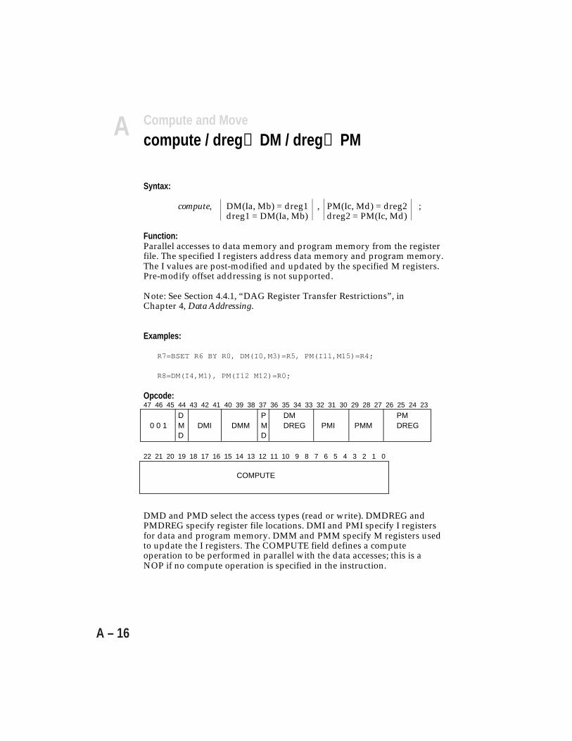
Instruction Set ReferenceA
A – 16
Compute and Move
compute / dreg↔DM / dreg↔PM
Syntax:
compute, DM(Ia, Mb) = dreg1 , PM(Ic, Md) = dreg2 ;dreg1 = DM(Ia, Mb) dreg2 = PM(Ic, Md)
Function:Parallel accesses to data memory and program memory from the registerfile. The specified I registers address data memory and program memory.The I values are post-modified and updated by the specified M registers.Pre-modify offset addressing is not supported.
Note: See Section 4.4.1, “DAG Register Transfer Restrictions”, inChapter 4, Data Addressing.
Examples:
R7=BSET R6 BY R0, DM(I0,M3)=R5, PM(I11,M15)=R4;
R8=DM(I4,M1), PM(I12 M12)=R0;
Opcode:47 46 45 44 43 42 41 40 39 38 37 36 35 34 33 32 31 30 29 28 27 26 25 24 23
D P DM PM 0 0 1 M DMI DMM M DREG PMI PMM DREG
D D
22 21 20 19 18 17 16 15 14 13 12 11 10 9 8 7 6 5 4 3 2 1 0
COMPUTE
DMD and PMD select the access types (read or write). DMDREG andPMDREG specify register file locations. DMI and PMI specify I registersfor data and program memory. DMM and PMM specify M registers usedto update the I registers. The COMPUTE field defines a computeoperation to be performed in parallel with the data accesses; this is aNOP if no compute operation is specified in the instruction.
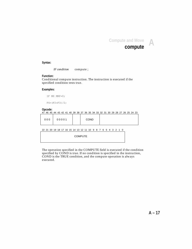
AInstruction Set Reference
A – 17
Syntax:
IF condition compute ;
Function:Conditional compute instruction. The instruction is executed if thespecified condition tests true.
Examples:
IF MS MRF=0;
F6=(F2+F3)/2;
Opcode:47 46 45 44 43 42 41 40 39 38 37 36 35 34 33 32 31 30 29 28 27 26 25 24 23
0 0 0 0 0 0 0 1 COND
22 21 20 19 18 17 16 15 14 13 12 11 10 9 8 7 6 5 4 3 2 1 0
COMPUTE
The operation specified in the COMPUTE field is executed if the conditionspecified by COND is true. If no condition is specified in the instruction,COND is the TRUE condition, and the compute operation is alwaysexecuted.
Compute and Movecompute
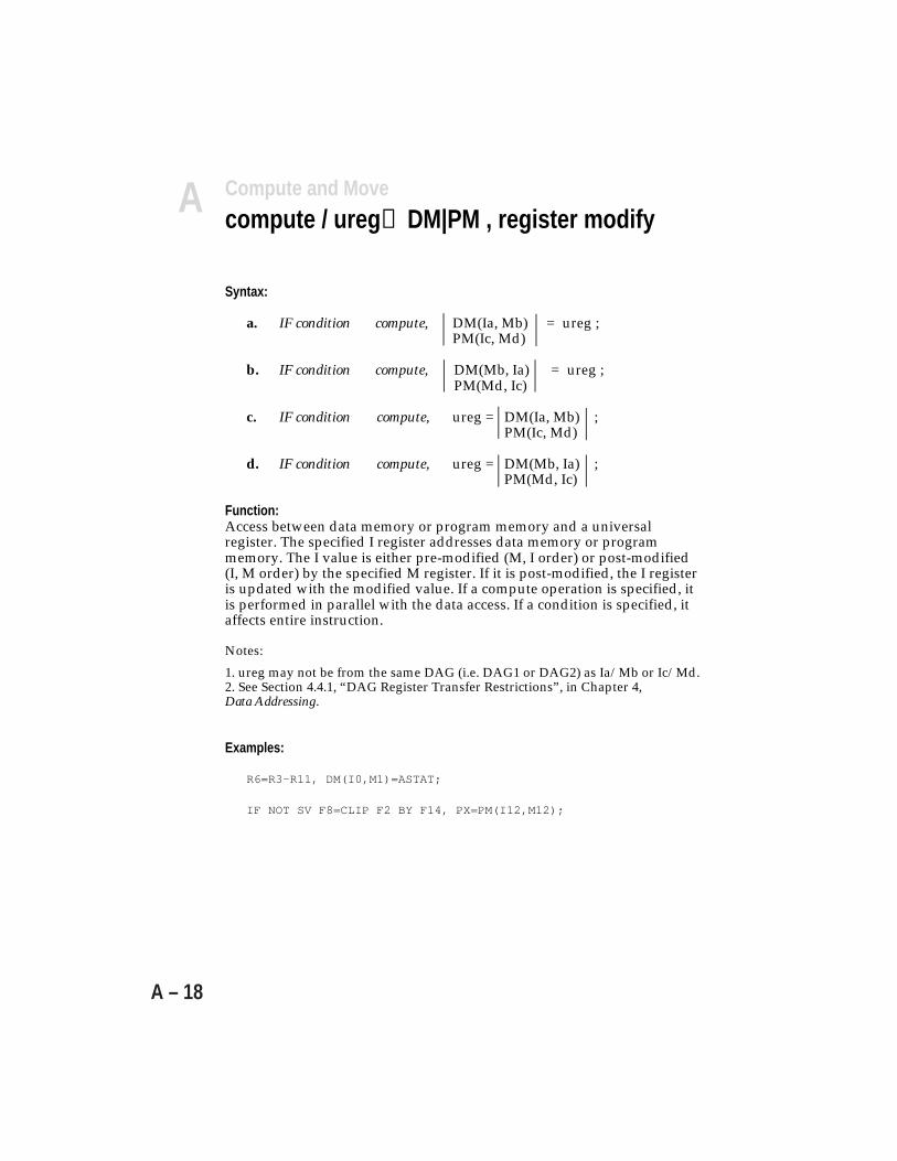
Instruction Set ReferenceA
A – 18
Syntax:
a. IF condition compute, DM(Ia, Mb) = ureg ;PM(Ic, Md)
b. IF condition compute, DM(Mb, Ia) = ureg ;PM(Md, Ic)
c. IF condition compute, ureg = DM(Ia, Mb) ;PM(Ic, Md)
d. IF condition compute, ureg = DM(Mb, Ia) ;PM(Md, Ic)
Function:Access between data memory or program memory and a universalregister. The specified I register addresses data memory or programmemory. The I value is either pre-modified (M, I order) or post-modified(I, M order) by the specified M register. If it is post-modified, the I registeris updated with the modified value. If a compute operation is specified, itis performed in parallel with the data access. If a condition is specified, itaffects entire instruction.
Notes:
1. ureg may not be from the same DAG (i.e. DAG1 or DAG2) as Ia/Mb or Ic/Md.2. See Section 4.4.1, “DAG Register Transfer Restrictions”, in Chapter 4,Data Addressing.
Examples:
R6=R3-R11, DM(I0,M1)=ASTAT;
IF NOT SV F8=CLIP F2 BY F14, PX=PM(I12,M12);
Compute and Move
compute / ureg↔DM|PM , register modify
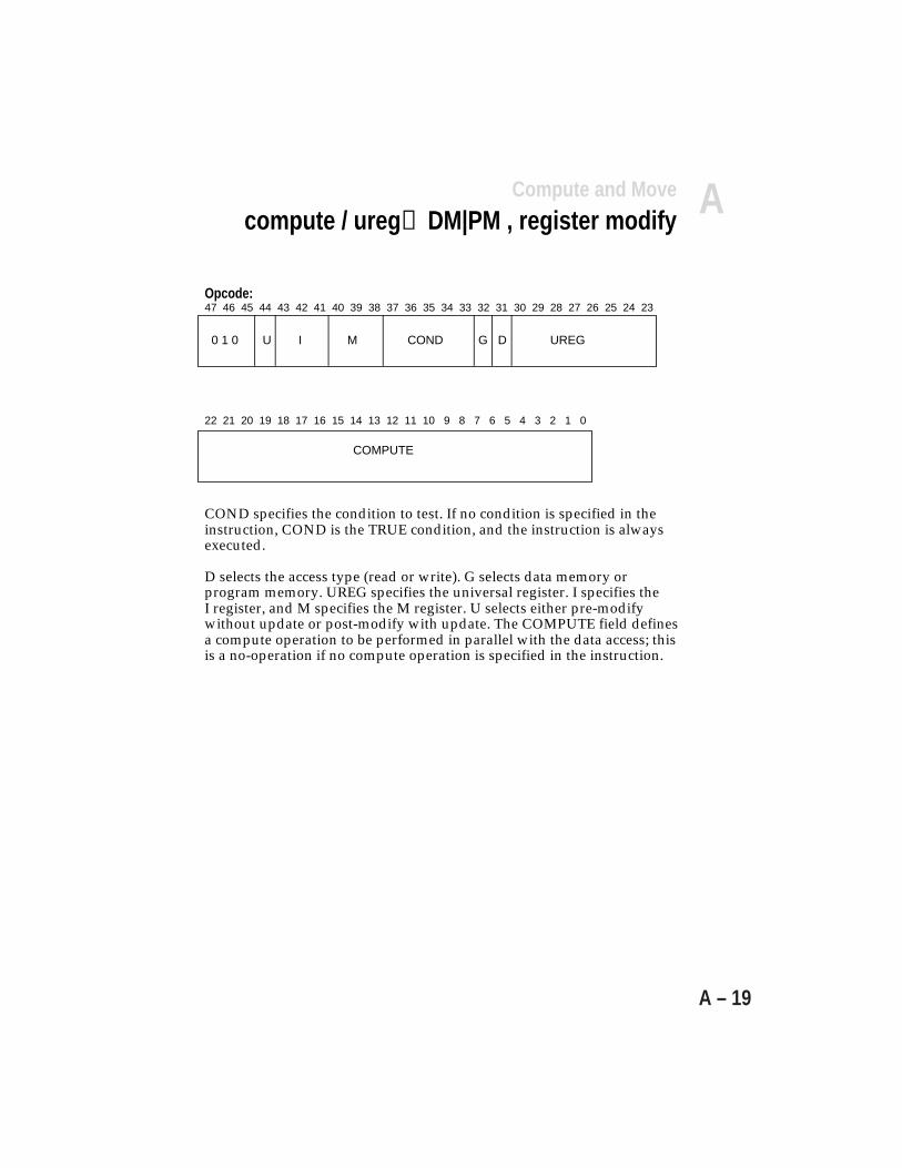
AInstruction Set Reference
A – 19
Compute and Move
compute / ureg↔DM|PM , register modify
Opcode:47 46 45 44 43 42 41 40 39 38 37 36 35 34 33 32 31 30 29 28 27 26 25 24 23
0 1 0 U I M COND G D UREG
22 21 20 19 18 17 16 15 14 13 12 11 10 9 8 7 6 5 4 3 2 1 0
COMPUTE
COND specifies the condition to test. If no condition is specified in theinstruction, COND is the TRUE condition, and the instruction is alwaysexecuted.
D selects the access type (read or write). G selects data memory orprogram memory. UREG specifies the universal register. I specifies theI register, and M specifies the M register. U selects either pre-modifywithout update or post-modify with update. The COMPUTE field definesa compute operation to be performed in parallel with the data access; thisis a no-operation if no compute operation is specified in the instruction.

Instruction Set ReferenceA
A – 20
Compute and Move
compute / dreg↔DM|PM , immediate modify
Syntax:
a. IF condition compute, DM(Ia, <data6>) = dreg ;PM(Ic, <data6>)
b. IF condition compute, DM(<data6>, Ia) = dreg ;PM(<data6>, Ic)
c. IF condition compute, dreg = DM(Ia, <data6>) ;PM(Ic, <data6>)
d. IF condition compute, dreg = DM(<data6>, Ia) ;PM(<data6>, Ic)
Function:Access between data memory or program memory and the register file.The specified I register addresses data memory or program memory. The Ivalue is either pre-modified (data order, I) or post-modified (I, data order)by the specified immediate data. If it is post-modified, the I register isupdated with the modified value. If a compute operation is specified, it isperformed in parallel with the data access. If a condition is specified, itaffects entire instruction.
Note: See Section 4.4.1, “DAG Register Transfer Restrictions”, inChapter 4, Data Addressing.
Examples:
IF FLAG0_IN F1=F5*F12, F11=PM(I10,40);
R12=R3 AND R1, DM(6,I1)=R6;
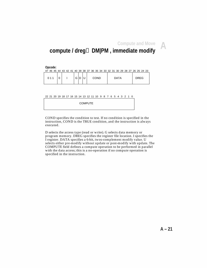
AInstruction Set Reference
A – 21
Compute and Move
compute / dreg↔DM|PM , immediate modify
Opcode:47 46 45 44 43 42 41 40 39 38 37 36 35 34 33 32 31 30 29 28 27 26 25 24 23
0 1 1 0 I G D U COND DATA DREG
22 21 20 19 18 17 16 15 14 13 12 11 10 9 8 7 6 5 4 3 2 1 0
COMPUTE
COND specifies the condition to test. If no condition is specified in theinstruction, COND is the TRUE condition, and the instruction is alwaysexecuted.
D selects the access type (read or write). G selects data memory orprogram memory. DREG specifies the register file location. I specifies theI register. DATA specifies a 6-bit, twos-complement modify value. Uselects either pre-modify without update or post-modify with update. TheCOMPUTE field defines a compute operation to be performed in parallelwith the data access; this is a no-operation if no compute operation isspecified in the instruction.

Instruction Set ReferenceA
A – 22
Compute and Move
compute / ureg↔ureg
Syntax:
IF condition compute, ureg1 = ureg2 ;
Function:Transfer from one universal register to another. If a compute operation isspecified, it is performed in parallel with the data access. If a condition isspecified, it affects entire instruction.
Examples:
IF TF MRF=R2*R6(SSFR), M4=R0;
LCNTR=L7;
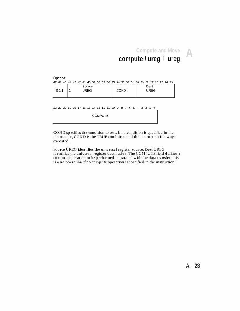
AInstruction Set Reference
A – 23
Opcode:47 46 45 44 43 42 41 40 39 38 37 36 35 34 33 32 31 30 29 28 27 26 25 24 23
Source Dest 0 1 1 1 UREG COND UREG
22 21 20 19 18 17 16 15 14 13 12 11 10 9 8 7 6 5 4 3 2 1 0
COMPUTE
COND specifies the condition to test. If no condition is specified in theinstruction, COND is the TRUE condition, and the instruction is alwaysexecuted.
Source UREG identifies the universal register source. Dest UREGidentifies the universal register destination. The COMPUTE field defines acompute operation to be performed in parallel with the data transfer; thisis a no-operation if no compute operation is specified in the instruction.
Compute and Move
compute / ureg↔ureg
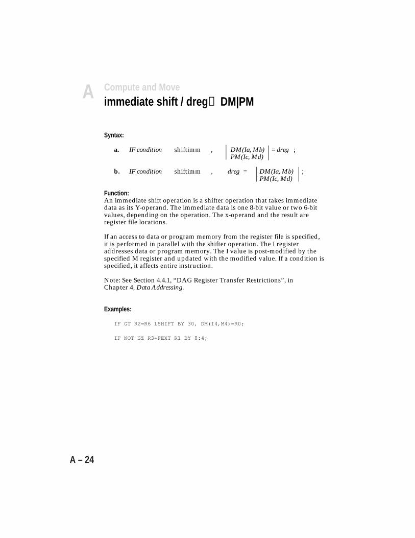
Instruction Set ReferenceA
A – 24
Compute and Move
immediate shift / dreg↔DM|PM
Syntax:
a. IF condition shiftimm , DM(Ia, Mb) = dreg ;PM(Ic, Md)
b. IF condition shiftimm , dreg = DM(Ia, Mb) ;PM(Ic, Md)
Function:An immediate shift operation is a shifter operation that takes immediatedata as its Y-operand. The immediate data is one 8-bit value or two 6-bitvalues, depending on the operation. The x-operand and the result areregister file locations.
If an access to data or program memory from the register file is specified,it is performed in parallel with the shifter operation. The I registeraddresses data or program memory. The I value is post-modified by thespecified M register and updated with the modified value. If a condition isspecified, it affects entire instruction.
Note: See Section 4.4.1, “DAG Register Transfer Restrictions”, inChapter 4, Data Addressing.
Examples:
IF GT R2=R6 LSHIFT BY 30, DM(I4,M4)=R0;
IF NOT SZ R3=FEXT R1 BY 8:4;
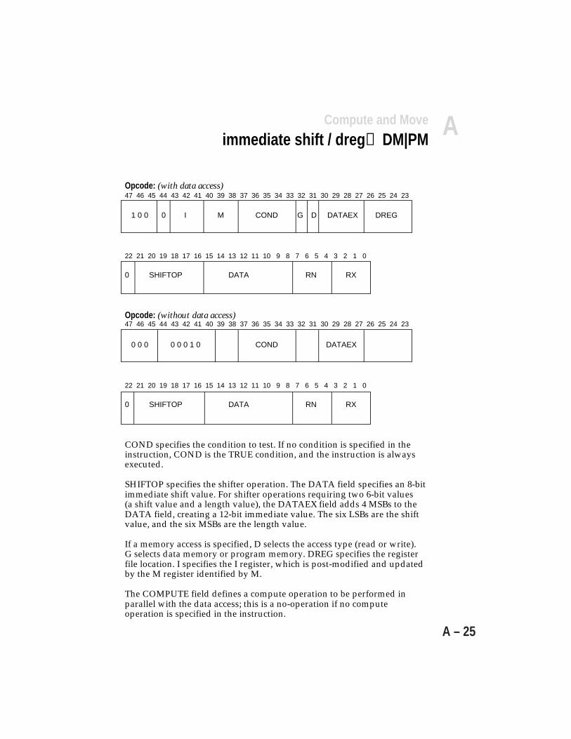
AInstruction Set Reference
A – 25
Opcode: (with data access)47 46 45 44 43 42 41 40 39 38 37 36 35 34 33 32 31 30 29 28 27 26 25 24 23
1 0 0 0 I M COND G D DATAEX DREG
22 21 20 19 18 17 16 15 14 13 12 11 10 9 8 7 6 5 4 3 2 1 0
0 SHIFTOP DATA RN RX
Opcode: (without data access)47 46 45 44 43 42 41 40 39 38 37 36 35 34 33 32 31 30 29 28 27 26 25 24 23
0 0 0 0 0 0 1 0 COND DATAEX
22 21 20 19 18 17 16 15 14 13 12 11 10 9 8 7 6 5 4 3 2 1 0
0 SHIFTOP DATA RN RX
COND specifies the condition to test. If no condition is specified in theinstruction, COND is the TRUE condition, and the instruction is alwaysexecuted.
SHIFTOP specifies the shifter operation. The DATA field specifies an 8-bitimmediate shift value. For shifter operations requiring two 6-bit values(a shift value and a length value), the DATAEX field adds 4 MSBs to theDATA field, creating a 12-bit immediate value. The six LSBs are the shiftvalue, and the six MSBs are the length value.
If a memory access is specified, D selects the access type (read or write).G selects data memory or program memory. DREG specifies the registerfile location. I specifies the I register, which is post-modified and updatedby the M register identified by M.
The COMPUTE field defines a compute operation to be performed inparallel with the data access; this is a no-operation if no computeoperation is specified in the instruction.
Compute and Move
immediate shift / dreg↔DM|PM

Instruction Set ReferenceA
A – 26
Syntax:
IF condition compute, MODIFY (Ia, Mb) ;(Ic, Md)
Function:Update of the specified I register by the specified M register. If a computeoperation is specified, it is performed in parallel with the data access. If acondition is specified, it affects entire instruction.
Note: See Section 4.4.1, “DAG Register Transfer Restrictions”, inChapter 4, Data Addressing.
Examples:
IF NOT FLAG2_IN R4=R6*R12(SUF), MODIFY(I10,M8);
IF NOT LCE MODIFY(I3,M1);
Opcode:47 46 45 44 43 42 41 40 39 38 37 36 35 34 33 32 31 30 29 28 27 26 25 24 23
0 0 0 0 0 1 0 0 G COND I M
22 21 20 19 18 17 16 15 14 13 12 11 10 9 8 7 6 5 4 3 2 1 0
COMPUTE
COND specifies the condition to test. If no condition is specified in theinstruction, COND is the TRUE condition, and the instruction is alwaysexecuted.
G selects DAG1 or DAG2. I specifies the I register, and M specifies theM register. The COMPUTE field defines a compute operation to beperformed in parallel with the data access; this is a no-operation if nocompute operation is specified in the instruction.
Compute and Movecompute / modify
AInstruction Set Reference
A – 27
Group II.Program Flow Control8. Direct (or PC-relative) jump/call, optional condition ........................................................A-28
9. Indirect (or PC-relative) jump/call, optional condition, optional compute operation ........A-30
10. Indirect (or PC-relative) jump or optional compute operation with transfer betweendata memory and register file..........................................................................................A-32
11. Return from subroutine or interrupt, optional condition, optional compute operation .....A-34
12. Load loop counter, do loop until loop counter expired ....................................................A-36
13. Do until termination .........................................................................................................A-38
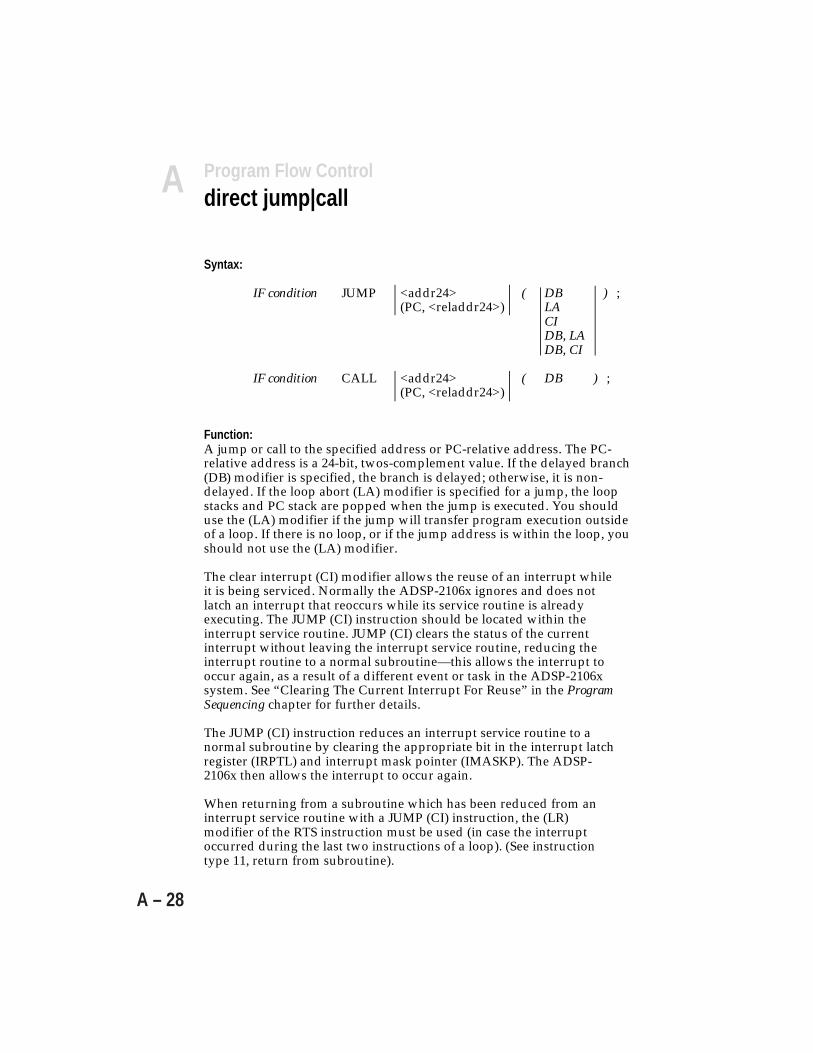
Instruction Set ReferenceA
A – 28
Program Flow Controldirect jump|call
Syntax:
IF condition JUMP <addr24> ( DB ) ;(PC, <reladdr24>) LA
CIDB, LADB, CI
IF condition CALL <addr24> ( DB ) ;(PC, <reladdr24>)
Function:A jump or call to the specified address or PC-relative address. The PC-relative address is a 24-bit, twos-complement value. If the delayed branch(DB) modifier is specified, the branch is delayed; otherwise, it is non-delayed. If the loop abort (LA) modifier is specified for a jump, the loopstacks and PC stack are popped when the jump is executed. You shoulduse the (LA) modifier if the jump will transfer program execution outsideof a loop. If there is no loop, or if the jump address is within the loop, youshould not use the (LA) modifier.
The clear interrupt (CI) modifier allows the reuse of an interrupt whileit is being serviced. Normally the ADSP-2106x ignores and does notlatch an interrupt that reoccurs while its service routine is alreadyexecuting. The JUMP (CI) instruction should be located within theinterrupt service routine. JUMP (CI) clears the status of the currentinterrupt without leaving the interrupt service routine, reducing theinterrupt routine to a normal subroutine—this allows the interrupt tooccur again, as a result of a different event or task in the ADSP-2106xsystem. See “Clearing The Current Interrupt For Reuse” in the ProgramSequencing chapter for further details.
The JUMP (CI) instruction reduces an interrupt service routine to anormal subroutine by clearing the appropriate bit in the interrupt latchregister (IRPTL) and interrupt mask pointer (IMASKP). The ADSP-2106x then allows the interrupt to occur again.
When returning from a subroutine which has been reduced from aninterrupt service routine with a JUMP (CI) instruction, the (LR)modifier of the RTS instruction must be used (in case the interruptoccurred during the last two instructions of a loop). (See instructiontype 11, return from subroutine).
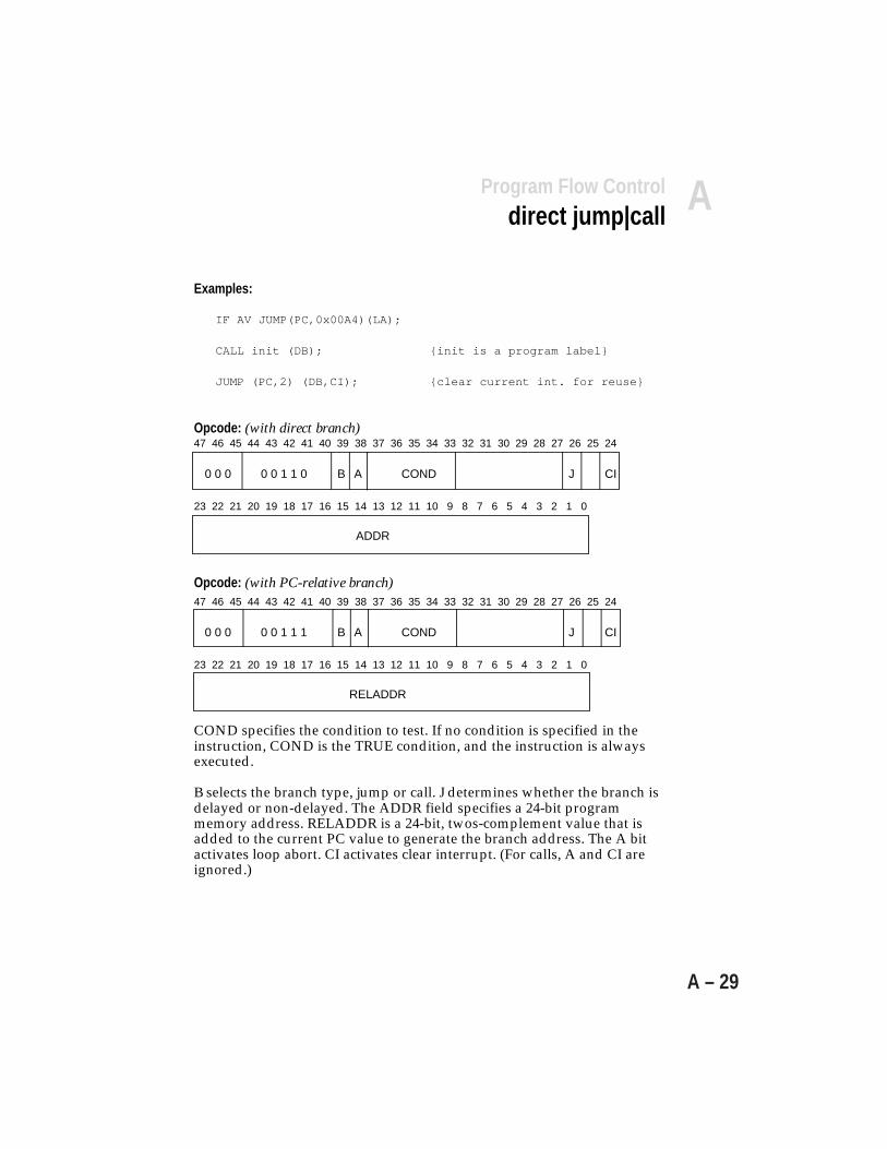
AInstruction Set Reference
A – 29
Examples:
IF AV JUMP(PC,0x00A4)(LA);
CALL init (DB); init is a program label
JUMP (PC,2) (DB,CI); clear current int. for reuse
Opcode: (with direct branch)47 46 45 44 43 42 41 40 39 38 37 36 35 34 33 32 31 30 29 28 27 26 25 24
0 0 0 0 0 1 1 0 B A COND J CI
23 22 21 20 19 18 17 16 15 14 13 12 11 10 9 8 7 6 5 4 3 2 1 0
ADDR
Opcode: (with PC-relative branch)47 46 45 44 43 42 41 40 39 38 37 36 35 34 33 32 31 30 29 28 27 26 25 24
0 0 0 0 0 1 1 1 B A COND J CI
23 22 21 20 19 18 17 16 15 14 13 12 11 10 9 8 7 6 5 4 3 2 1 0
RELADDR
COND specifies the condition to test. If no condition is specified in theinstruction, COND is the TRUE condition, and the instruction is alwaysexecuted.
B selects the branch type, jump or call. J determines whether the branch isdelayed or non-delayed. The ADDR field specifies a 24-bit programmemory address. RELADDR is a 24-bit, twos-complement value that isadded to the current PC value to generate the branch address. The A bitactivates loop abort. CI activates clear interrupt. (For calls, A and CI areignored.)
Program Flow Controldirect jump|call
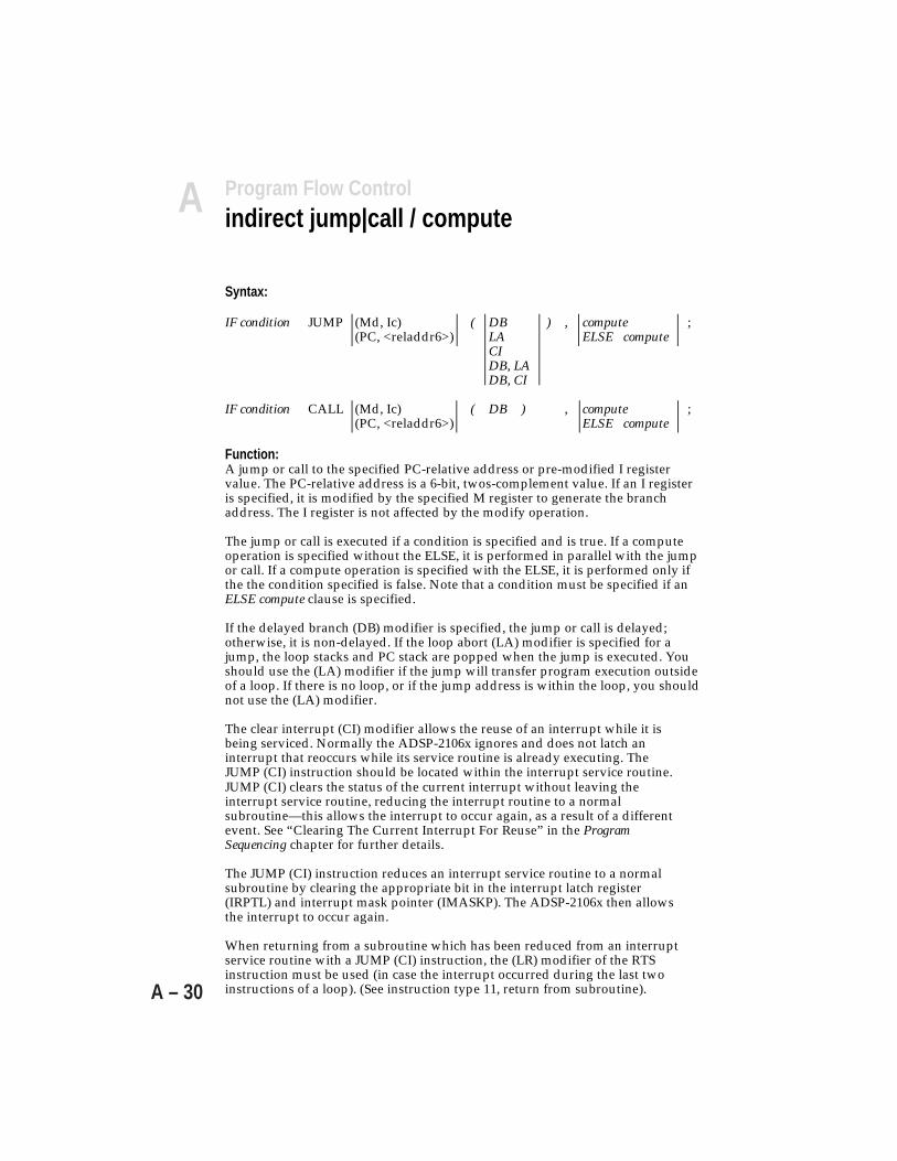
Instruction Set ReferenceA
A – 30
Program Flow Controlindirect jump|call / compute
Syntax:
IF condition JUMP (Md, Ic) ( DB ) , compute ;(PC, <reladdr6>) LA ELSE compute
CIDB, LADB, CI
IF condition CALL (Md, Ic) ( DB ) , compute ;(PC, <reladdr6>) ELSE compute
Function:A jump or call to the specified PC-relative address or pre-modified I registervalue. The PC-relative address is a 6-bit, twos-complement value. If an I registeris specified, it is modified by the specified M register to generate the branchaddress. The I register is not affected by the modify operation.
The jump or call is executed if a condition is specified and is true. If a computeoperation is specified without the ELSE, it is performed in parallel with the jumpor call. If a compute operation is specified with the ELSE, it is performed only ifthe the condition specified is false. Note that a condition must be specified if anELSE compute clause is specified.
If the delayed branch (DB) modifier is specified, the jump or call is delayed;otherwise, it is non-delayed. If the loop abort (LA) modifier is specified for ajump, the loop stacks and PC stack are popped when the jump is executed. Youshould use the (LA) modifier if the jump will transfer program execution outsideof a loop. If there is no loop, or if the jump address is within the loop, you shouldnot use the (LA) modifier.
The clear interrupt (CI) modifier allows the reuse of an interrupt while it isbeing serviced. Normally the ADSP-2106x ignores and does not latch aninterrupt that reoccurs while its service routine is already executing. TheJUMP (CI) instruction should be located within the interrupt service routine.JUMP (CI) clears the status of the current interrupt without leaving theinterrupt service routine, reducing the interrupt routine to a normalsubroutine—this allows the interrupt to occur again, as a result of a differentevent. See “Clearing The Current Interrupt For Reuse” in the ProgramSequencing chapter for further details.
The JUMP (CI) instruction reduces an interrupt service routine to a normalsubroutine by clearing the appropriate bit in the interrupt latch register(IRPTL) and interrupt mask pointer (IMASKP). The ADSP-2106x then allowsthe interrupt to occur again.
When returning from a subroutine which has been reduced from an interruptservice routine with a JUMP (CI) instruction, the (LR) modifier of the RTSinstruction must be used (in case the interrupt occurred during the last twoinstructions of a loop). (See instruction type 11, return from subroutine).

AInstruction Set Reference
A – 31
Note: For indirect branches, see Section 4.4.1, “DAG Register TransferRestrictions”, in Chapter 4, Data Addressing.
Examples:JUMP(M8,I12), R6=R6-1;
IF EQ CALL(PC,17)(DB) , ELSE R6=R6-1;
Opcode: (with indirect branch)47 46 45 44 43 42 41 40 39 38 37 36 35 34 33 32 31 30 29 28 27 26 25 24 23
0 0 0 0 1 0 0 0 B A COND PMI PMM J E CI
22 21 20 19 18 17 16 15 14 13 12 11 10 9 8 7 6 5 4 3 2 1 0
COMPUTE
Opcode: (with PC-relative branch)47 46 45 44 43 42 41 40 39 38 37 36 35 34 33 32 31 30 29 28 27 26 25 24 23
0 0 0 0 1 0 0 1 B A COND RELADDR J E CI
22 21 20 19 18 17 16 15 14 13 12 11 10 9 8 7 6 5 4 3 2 1 0
COMPUTE
COND specifies the condition to test. If no condition is specified in theinstruction, COND is the true condition, and the instruction is always executed.E specifies whether or not an ELSE clause is used.
B selects the branch type, jump or call. J determines whether the branch isdelayed or non-delayed. The A bit activates loop abort. CI activates clearinterrupt. (For calls, A and CI are ignored.)
RELADDR is a 6-bit, twos-complement value that is added to the current PCvalue to generate the branch address. PMI specifies the I register for indirectbranches. The I register is pre-modified but not updated by the M registerspecified by PMM.
The COMPUTE field defines a compute operation to be performed in parallelwith the data access; this is a NOP if no compute operation is specified in theinstruction.
Program Flow Controlindirect jump|call / compute
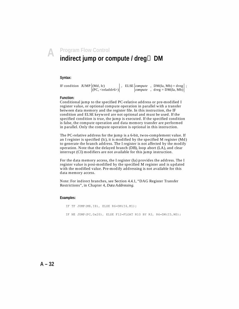
Instruction Set ReferenceA
A – 32
Program Flow Control
indirect jump or compute / dreg↔DM
Syntax:
IF condition JUMP (Md, Ic) , ELSE compute , DM(Ia, Mb) = dreg ;(PC, <reladdr6>) compute , dreg = DM(Ia, Mb)
Function:Conditional jump to the specified PC-relative address or pre-modified Iregister value, or optional compute operation in parallel with a transferbetween data memory and the register file. In this instruction, the IFcondition and ELSE keyword are not optional and must be used. If thespecified condition is true, the jump is executed. If the specified conditionis false, the compute operation and data memory transfer are performedin parallel. Only the compute operation is optional in this instruction.
The PC-relative address for the jump is a 6-bit, twos-complement value. Ifan I register is specified (Ic), it is modified by the specified M register (Md)to generate the branch address. The I register is not affected by the modifyoperation. Note that the delayed branch (DB), loop abort (LA), and clearinterrupt (CI) modifiers are not available for this jump instruction.
For the data memory access, the I register (Ia) provides the address. The Iregister value is post-modified by the specified M register and is updatedwith the modified value. Pre-modify addressing is not available for thisdata memory access.
Note: For indirect branches, see Section 4.4.1, “DAG Register TransferRestrictions”, in Chapter 4, Data Addressing.
Examples:
IF TF JUMP(M8,I8), ELSE R6=DM(I6,M1);
IF NE JUMP(PC,0x20), ELSE F12=FLOAT R10 BY R3, R6=DM(I5,M0);

AInstruction Set Reference
A – 33
Opcode: (with indirect jump)47 46 45 44 43 42 41 40 39 38 37 36 35 34 33 32 31 30 29 28 27 26 25 24 23
1 1 0 D DMI DMM COND PMI PMM DREG
22 21 20 19 18 17 16 15 14 13 12 11 10 9 8 7 6 5 4 3 2 1 0
COMPUTE
Opcode:(with PC-relative jump)47 46 45 44 43 42 41 40 39 38 37 36 35 34 33 32 31 30 29 28 27 26 25 24 23
1 1 1 D DMI DMM COND RELADDR DREG
22 21 20 19 18 17 16 15 14 13 12 11 10 9 8 7 6 5 4 3 2 1 0
COMPUTE
COND specifies the condition to test.
PMI specifies the I register for indirect branches. The I register is pre-modified but not updated by the M register specified by PMM. RELADDRis a 6-bit, twos-complement value that is added to the current PC value togenerate the branch address.
D selects the data memory access type (read or write). DREG specifies theregister file location. DMI specifies the I register, which is post-modifiedand updated by the M register identified by DMM.
The COMPUTE field defines a compute operation to be performed inparallel with the data access; this is a NOP if no compute operation isspecified in the instruction.
Program Flow Control
indirect jump / compute / dreg↔DM
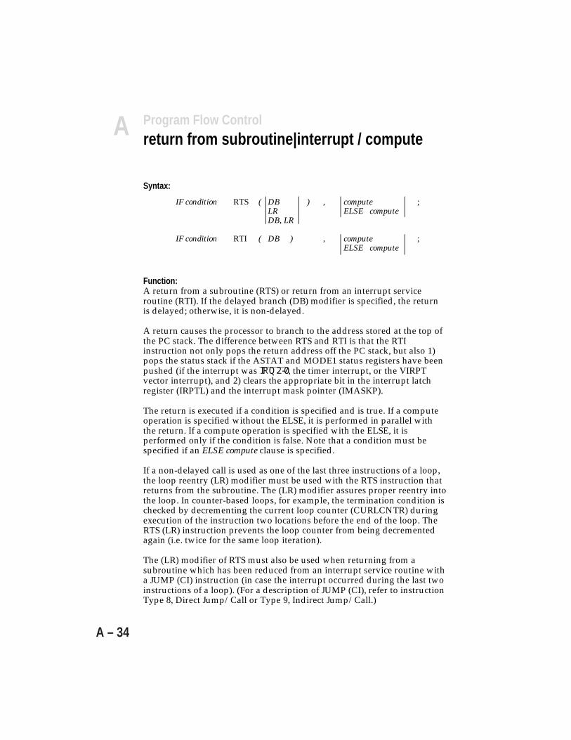
Instruction Set ReferenceA
A – 34
Program Flow Controlreturn from subroutine|interrupt / compute
Syntax:
IF condition RTS ( DB ) , compute ;LR ELSE computeDB, LR
IF condition RTI ( DB ) , compute ;ELSE compute
Function:A return from a subroutine (RTS) or return from an interrupt serviceroutine (RTI). If the delayed branch (DB) modifier is specified, the returnis delayed; otherwise, it is non-delayed.
A return causes the processor to branch to the address stored at the top ofthe PC stack. The difference between RTS and RTI is that the RTIinstruction not only pops the return address off the PC stack, but also 1)pops the status stack if the ASTAT and MODE1 status registers have beenpushed (if the interrupt was IRQ2-0, the timer interrupt, or the VIRPTvector interrupt), and 2) clears the appropriate bit in the interrupt latchregister (IRPTL) and the interrupt mask pointer (IMASKP).
The return is executed if a condition is specified and is true. If a computeoperation is specified without the ELSE, it is performed in parallel withthe return. If a compute operation is specified with the ELSE, it isperformed only if the condition is false. Note that a condition must bespecified if an ELSE compute clause is specified.
If a non-delayed call is used as one of the last three instructions of a loop,the loop reentry (LR) modifier must be used with the RTS instruction thatreturns from the subroutine. The (LR) modifier assures proper reentry intothe loop. In counter-based loops, for example, the termination condition ischecked by decrementing the current loop counter (CURLCNTR) duringexecution of the instruction two locations before the end of the loop. TheRTS (LR) instruction prevents the loop counter from being decrementedagain (i.e. twice for the same loop iteration).
The (LR) modifier of RTS must also be used when returning from asubroutine which has been reduced from an interrupt service routine witha JUMP (CI) instruction (in case the interrupt occurred during the last twoinstructions of a loop). (For a description of JUMP (CI), refer to instructionType 8, Direct Jump/Call or Type 9, Indirect Jump/Call.)
IF condition RTS ( DB ) , compute ;LR ELSE computeDB, LR
IF condition RTI ( DB ) , compute ;ELSE compute
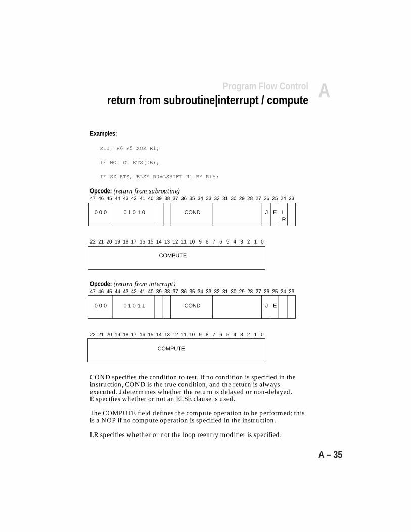
AInstruction Set Reference
A – 35
Examples:
RTI, R6=R5 XOR R1;
IF NOT GT RTS(DB);
IF SZ RTS, ELSE R0=LSHIFT R1 BY R15;
Opcode: (return from subroutine)47 46 45 44 43 42 41 40 39 38 37 36 35 34 33 32 31 30 29 28 27 26 25 24 23
0 0 0 0 1 0 1 0 COND J E LR
22 21 20 19 18 17 16 15 14 13 12 11 10 9 8 7 6 5 4 3 2 1 0
COMPUTE
Opcode: (return from interrupt)47 46 45 44 43 42 41 40 39 38 37 36 35 34 33 32 31 30 29 28 27 26 25 24 23
0 0 0 0 1 0 1 1 COND J E
22 21 20 19 18 17 16 15 14 13 12 11 10 9 8 7 6 5 4 3 2 1 0
COMPUTE
COND specifies the condition to test. If no condition is specified in theinstruction, COND is the true condition, and the return is alwaysexecuted. J determines whether the return is delayed or non-delayed.E specifies whether or not an ELSE clause is used.
The COMPUTE field defines the compute operation to be performed; thisis a NOP if no compute operation is specified in the instruction.
LR specifies whether or not the loop reentry modifier is specified.
Program Flow Controlreturn from subroutine|interrupt / compute
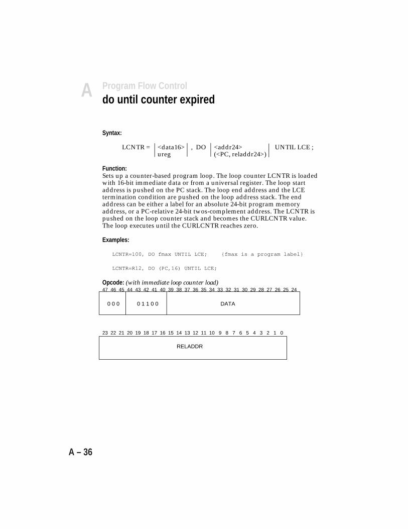
Instruction Set ReferenceA
A – 36
Program Flow Controldo until counter expired
Syntax:
LCNTR = <data16> , DO <addr24> UNTIL LCE ;ureg (<PC, reladdr24>)
Function:Sets up a counter-based program loop. The loop counter LCNTR is loadedwith 16-bit immediate data or from a universal register. The loop startaddress is pushed on the PC stack. The loop end address and the LCEtermination condition are pushed on the loop address stack. The endaddress can be either a label for an absolute 24-bit program memoryaddress, or a PC-relative 24-bit twos-complement address. The LCNTR ispushed on the loop counter stack and becomes the CURLCNTR value.The loop executes until the CURLCNTR reaches zero.
Examples:
LCNTR=100, DO fmax UNTIL LCE; fmax is a program label
LCNTR=R12, DO (PC,16) UNTIL LCE;
Opcode: (with immediate loop counter load)47 46 45 44 43 42 41 40 39 38 37 36 35 34 33 32 31 30 29 28 27 26 25 24
0 0 0 0 1 1 0 0 DATA
23 22 21 20 19 18 17 16 15 14 13 12 11 10 9 8 7 6 5 4 3 2 1 0
RELADDR
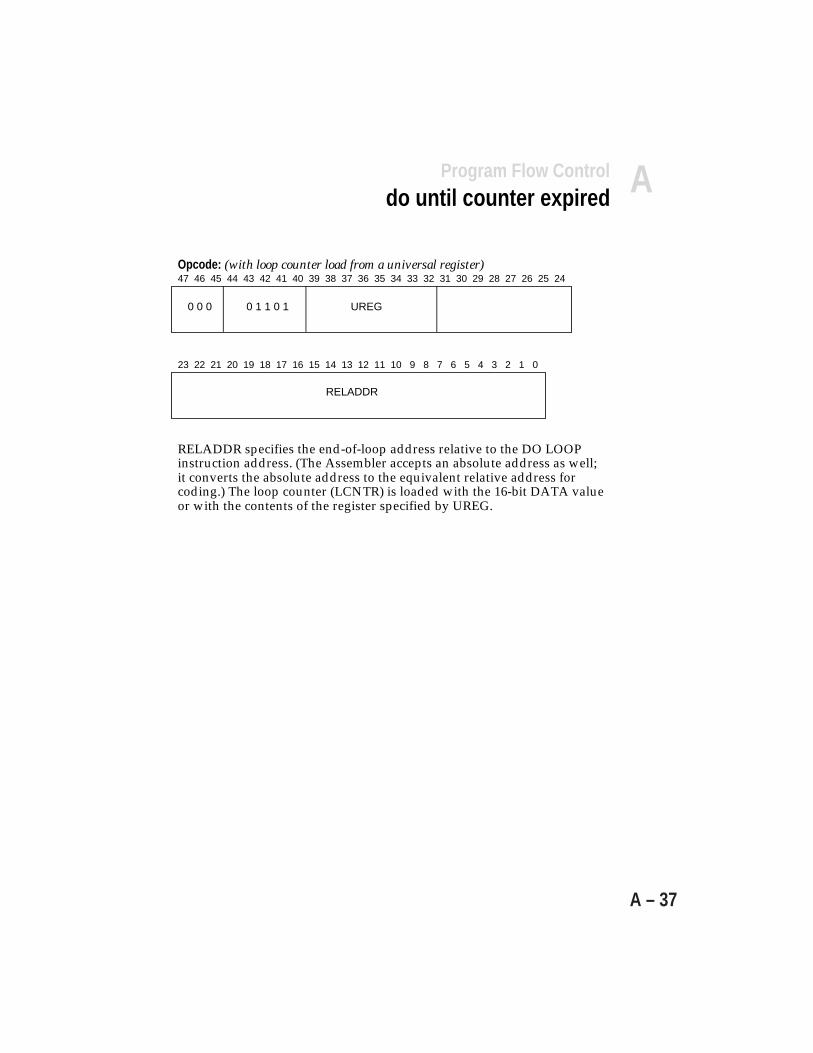
AInstruction Set Reference
A – 37
Opcode: (with loop counter load from a universal register)47 46 45 44 43 42 41 40 39 38 37 36 35 34 33 32 31 30 29 28 27 26 25 24
0 0 0 0 1 1 0 1 UREG
23 22 21 20 19 18 17 16 15 14 13 12 11 10 9 8 7 6 5 4 3 2 1 0
RELADDR
RELADDR specifies the end-of-loop address relative to the DO LOOPinstruction address. (The Assembler accepts an absolute address as well;it converts the absolute address to the equivalent relative address forcoding.) The loop counter (LCNTR) is loaded with the 16-bit DATA valueor with the contents of the register specified by UREG.
Program Flow Controldo until counter expired
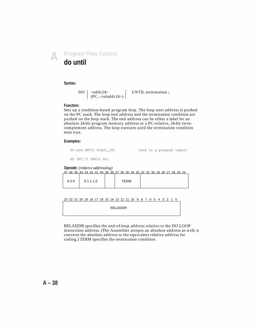
Instruction Set ReferenceA
A – 38
Program Flow Controldo until
Syntax:
DO <addr24> UNTIL termination ;(PC, <reladdr24>)
Function:Sets up a condition-based program loop. The loop start address is pushedon the PC stack. The loop end address and the termination condition arepushed on the loop stack. The end address can be either a label for anabsolute 24-bit program memory address or a PC-relative, 24-bit twos-complement address. The loop executes until the termination conditiontests true.
Examples:
DO end UNTIL FLAG1_IN; end is a program label
DO (PC,7) UNTIL AC;
Opcode: (relative addressing)47 46 45 44 43 42 41 40 39 38 37 36 35 34 33 32 31 30 29 28 27 26 25 24
0 0 0 0 1 1 1 0 TERM
23 22 21 20 19 18 17 16 15 14 13 12 11 10 9 8 7 6 5 4 3 2 1 0
RELADDR
RELADDR specifies the end-of-loop address relative to the DO LOOPinstruction address. (The Assembler accepts an absolute address as well; itconverts the absolute address to the equivalent relative address forcoding.) TERM specifies the termination condition.
AInstruction Set Reference
A – 39
Group III.Immediate Move14. Transfer between data or program memory and universal register, direct
addressing, immediate address................................................................................A-40
15. Transfer between data or program memory and universal register, indirectaddressing, immediate modifier ................................................................................A-41
16. Immediate data write to data or program memory ....................................................A-42
17. Immediate data write to universal register ................................................................A-43
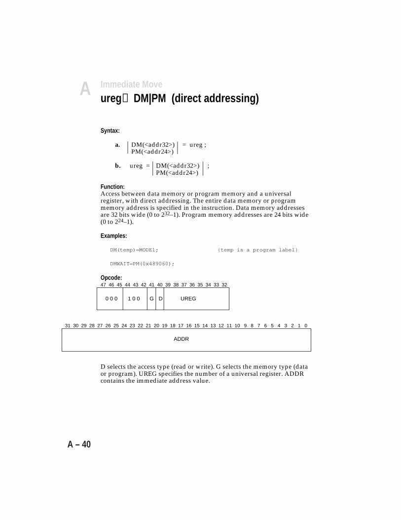
Instruction Set ReferenceA
A – 40
Immediate Move
ureg↔DM|PM (direct addressing)
Syntax:
a. DM(<addr32>) = ureg ;PM(<addr24>)
b. ureg = DM(<addr32>) ;PM(<addr24>)
Function:Access between data memory or program memory and a universalregister, with direct addressing. The entire data memory or programmemory address is specified in the instruction. Data memory addressesare 32 bits wide (0 to 232–1). Program memory addresses are 24 bits wide(0 to 224–1).
Examples:
DM(temp)=MODE1; temp is a program label
DMWAIT=PM(0x489060);
Opcode:47 46 45 44 43 42 41 40 39 38 37 36 35 34 33 32
0 0 0 1 0 0 G D UREG
31 30 29 28 27 26 25 24 23 22 21 20 19 18 17 16 15 14 13 12 11 10 9 8 7 6 5 4 3 2 1 0
ADDR
D selects the access type (read or write). G selects the memory type (dataor program). UREG specifies the number of a universal register. ADDRcontains the immediate address value.
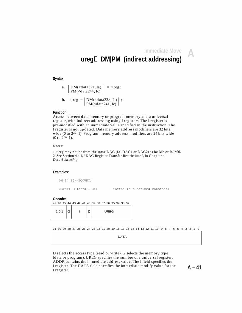
AInstruction Set Reference
A – 41
Syntax:
a. DM(<data32>, Ia) = ureg ;PM(<data24>, Ic)
b. ureg = DM(<data32>, Ia) ;PM(<data24>, Ic)
Function:Access between data memory or program memory and a universalregister, with indirect addressing using I registers. The I register ispre-modified with an immediate value specified in the instruction. TheI register is not updated. Data memory address modifiers are 32 bitswide (0 to 232–1). Program memory address modifiers are 24 bits wide(0 to 224–1).
Notes:
1. ureg may not be from the same DAG (i.e. DAG1 or DAG2) as Ia/Mb or Ic/Md.2. See Section 4.4.1, “DAG Register Transfer Restrictions”, in Chapter 4,Data Addressing.
Examples:
DM(24,I5)=TCOUNT;
USTAT1=PM(offs,I13); "offs" is a defined constant
Opcode:47 46 45 44 43 42 41 40 39 38 37 36 35 34 33 32
1 0 1 G I D UREG
31 30 29 28 27 26 25 24 23 22 21 20 19 18 17 16 15 14 13 12 11 10 9 8 7 6 5 4 3 2 1 0
DATA
Immediate Move
ureg↔DM|PM (indirect addressing)
D selects the access type (read or write). G selects the memory type(data or program). UREG specifies the number of a universal register.ADDR contains the immediate address value. The I field specifies theI register. The DATA field specifies the immediate modify value for theI register.
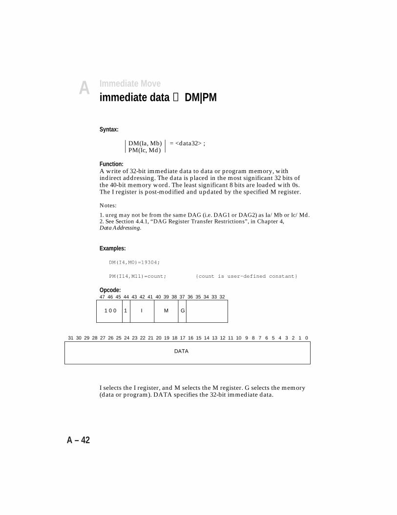
Instruction Set ReferenceA
A – 42
Immediate Move
immediate data → DM|PM
Syntax:
DM(Ia, Mb) = <data32> ;PM(Ic, Md)
Function:A write of 32-bit immediate data to data or program memory, withindirect addressing. The data is placed in the most significant 32 bits ofthe 40-bit memory word. The least significant 8 bits are loaded with 0s.The I register is post-modified and updated by the specified M register.
Notes:
1. ureg may not be from the same DAG (i.e. DAG1 or DAG2) as Ia/Mb or Ic/Md.2. See Section 4.4.1, “DAG Register Transfer Restrictions”, in Chapter 4,Data Addressing.
Examples:
DM(I4,M0)=19304;
PM(I14,M11)=count; count is user-defined constant
Opcode:47 46 45 44 43 42 41 40 39 38 37 36 35 34 33 32
1 0 0 1 I M G
31 30 29 28 27 26 25 24 23 22 21 20 19 18 17 16 15 14 13 12 11 10 9 8 7 6 5 4 3 2 1 0
DATA
I selects the I register, and M selects the M register. G selects the memory(data or program). DATA specifies the 32-bit immediate data.
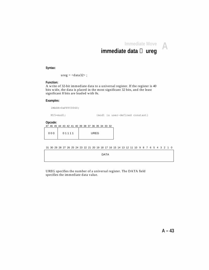
AInstruction Set Reference
A – 43
Syntax:
ureg = <data32> ;
Function:A write of 32-bit immediate data to a universal register. If the register is 40bits wide, the data is placed in the most significant 32 bits, and the leastsignificant 8 bits are loaded with 0s.
Examples:
IMASK=0xFFFC0060;
M15=mod1; mod1 is user-defined constant
Opcode:47 46 45 44 43 42 41 40 39 38 37 36 35 34 33 32
0 0 0 0 1 1 1 1 UREG
31 30 29 28 27 26 25 24 23 22 21 20 19 18 17 16 15 14 13 12 11 10 9 8 7 6 5 4 3 2 1 0
DATA
UREG specifies the number of a universal register. The DATA fieldspecifies the immediate data value.
Immediate Move
immediate data → ureg

Instruction Set ReferenceA
A – 44

AInstruction Set Reference
A – 45
Group IV.Miscellaneous18. System register bit manipulation ..............................................................................A-46
19. Immediate I register modify, with or without bit-reverse ...........................................A-48
20. Push or Pop of loop and/or status stacks .................................................................A-50
21. No Operation (NOP) .................................................................................................A-51
22. Idle ............................................................................................................................A-52
23. Idle16 ........................................................................................................................A-53
24. CJUMP/RFRAME (Compiler-generated instruction) ................................................A-54
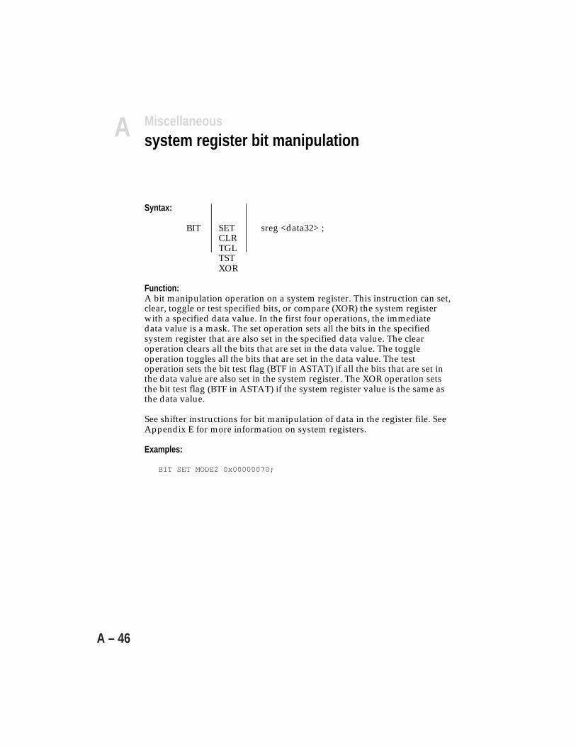
Instruction Set ReferenceA
A – 46
Miscellaneoussystem register bit manipulation
Syntax:
BIT SET sreg <data32> ;CLRTGLTSTXOR
Function:A bit manipulation operation on a system register. This instruction can set,clear, toggle or test specified bits, or compare (XOR) the system registerwith a specified data value. In the first four operations, the immediatedata value is a mask. The set operation sets all the bits in the specifiedsystem register that are also set in the specified data value. The clearoperation clears all the bits that are set in the data value. The toggleoperation toggles all the bits that are set in the data value. The testoperation sets the bit test flag (BTF in ASTAT) if all the bits that are set inthe data value are also set in the system register. The XOR operation setsthe bit test flag (BTF in ASTAT) if the system register value is the same asthe data value.
See shifter instructions for bit manipulation of data in the register file. SeeAppendix E for more information on system registers.
Examples:
BIT SET MODE2 0x00000070;
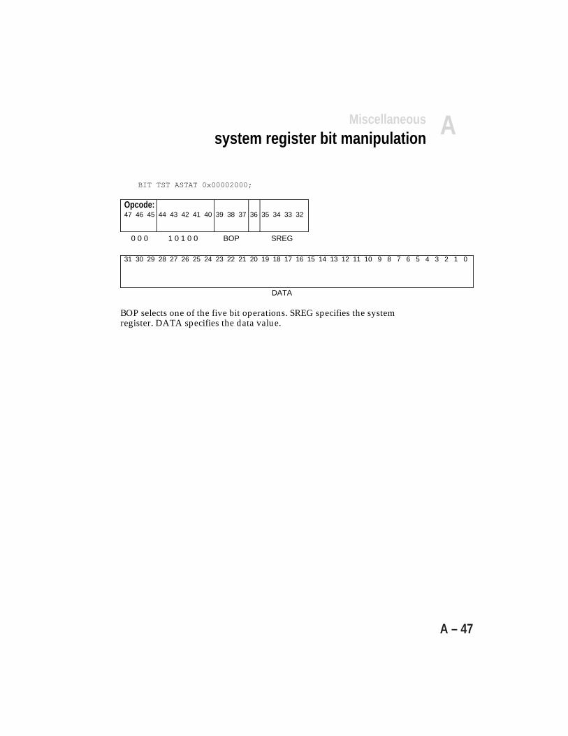
AInstruction Set Reference
A – 47
0 0 0 1 0 1 0 0 BOP SREG
31 30 29 28 27 26 25 24 23 22 21 20 19 18 17 16 15 14 13 12 11 10 9 8 7 6 5 4 3 2 1 0
BIT TST ASTAT 0x00002000;
Opcode:47 46 45 44 43 42 41 40 39 38 37 36 35 34 33 32
DATA
BOP selects one of the five bit operations. SREG specifies the systemregister. DATA specifies the data value.
Miscellaneoussystem register bit manipulation
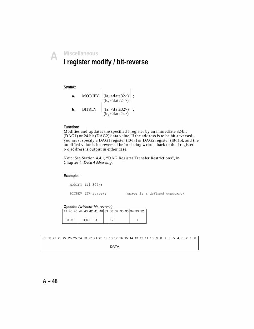
Instruction Set ReferenceA
A – 48
MiscellaneousI register modify / bit-reverse
Syntax:
a. MODIFY (Ia, <data32>) ;(Ic, <data24>)
b. BITREV (Ia, <data32>) ;(Ic, <data24>)
Function:Modifies and updates the specified I register by an immediate 32-bit(DAG1) or 24-bit (DAG2) data value. If the address is to be bit-reversed,you must specify a DAG1 register (I0-I7) or DAG2 register (I8-I15), and themodified value is bit-reversed before being written back to the I register.No address is output in either case.
Note: See Section 4.4.1, “DAG Register Transfer Restrictions”, inChapter 4, Data Addressing.
Examples:
MODIFY (I4,304);
BITREV (I7,space); space is a defined constant
Opcode: (without bit-reverse)47 46 45 44 43 42 41 40 39 38 37 36 35 34 33 32
0 0 0 1 0 1 1 0 G I
31 30 29 28 27 26 25 24 23 22 21 20 19 18 17 16 15 14 13 12 11 10 9 8 7 6 5 4 3 2 1 0
DATA

AInstruction Set Reference
A – 49
Opcode: (with bit-reverse)47 46 45 44 43 42 41 40 39 38 37 36 35 34 33 32
0 0 0 1 0 1 1 0 1 G I
31 30 29 28 27 26 25 24 23 22 21 20 19 18 17 16 15 14 13 12 11 10 9 8 7 6 5 4 3 2 1 0
DATA
MiscellaneousI register modify / bit-reverse
G selects the data address generator:
G=0 for DAG1G=1 for DAG2
I selects the I register:
I=0-7 for I0-I7 (for DAG1)I=0-7 for I8-I15 (for DAG2)
DATA specifies the immediate modifier.

Instruction Set ReferenceA
A – 50
Miscellaneouspush|pop stacks / flush cache
Syntax:
PUSH LOOP , PUSH STS , PUSH PCSTK , FLUSH CACHE ;POP POP POP
Function:Pushes or pops the loop address and loop counter stacks, the status stack,and/or the PC stack, and/or clear the instruction cache. Any of theseoptions may be combined in a single instruction.
Flushing the instruction cache invalidates all entries in the cache, with nolatency—the cache is cleared at the end of the cycle.
Examples:
PUSH LOOP, PUSH STS;
POP PCSTK, FLUSH CACHE;
Opcode:
47 46 45 44 43 42 41 40 39 38 37 36 35 34 33 32
L L S S P P F 0 0 0 1 0 1 1 1 P P P P P P C
U O U O U O
31 30 29 28 27 26 25 24 23 22 21 20 19 18 17 16 15 14 13 12 11 10 9 8 7 6 5 4 3 2 1 0
LPU pushes the loop stacks. LPO pops the loop stacks. SPU pushes thestatus stack. SPO pops the status stack. PPU pushes the PC stack. PPOpops the PC stack. FC causes a cache flush.
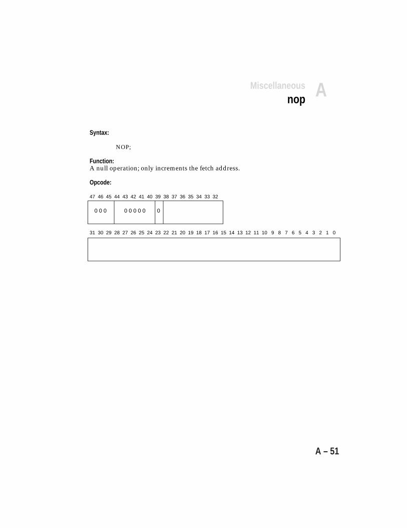
AInstruction Set Reference
A – 51
Syntax:
NOP;
Function:A null operation; only increments the fetch address.
Opcode:
47 46 45 44 43 42 41 40 39 38 37 36 35 34 33 32
0 0 0 0 0 0 0 0 0
31 30 29 28 27 26 25 24 23 22 21 20 19 18 17 16 15 14 13 12 11 10 9 8 7 6 5 4 3 2 1 0
Miscellaneousnop
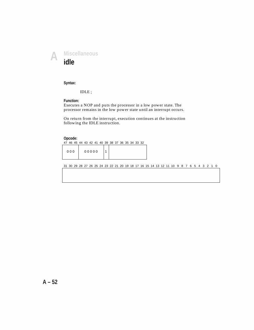
Instruction Set ReferenceA
A – 52
Miscellaneousidle
Opcode:47 46 45 44 43 42 41 40 39 38 37 36 35 34 33 32
0 0 0 0 0 0 0 0 1
Syntax:
IDLE ;
Function:Executes a NOP and puts the processor in a low power state. Theprocessor remains in the low power state until an interrupt occurs.
On return from the interrupt, execution continues at the instructionfollowing the IDLE instruction.
31 30 29 28 27 26 25 24 23 22 21 20 19 18 17 16 15 14 13 12 11 10 9 8 7 6 5 4 3 2 1 0
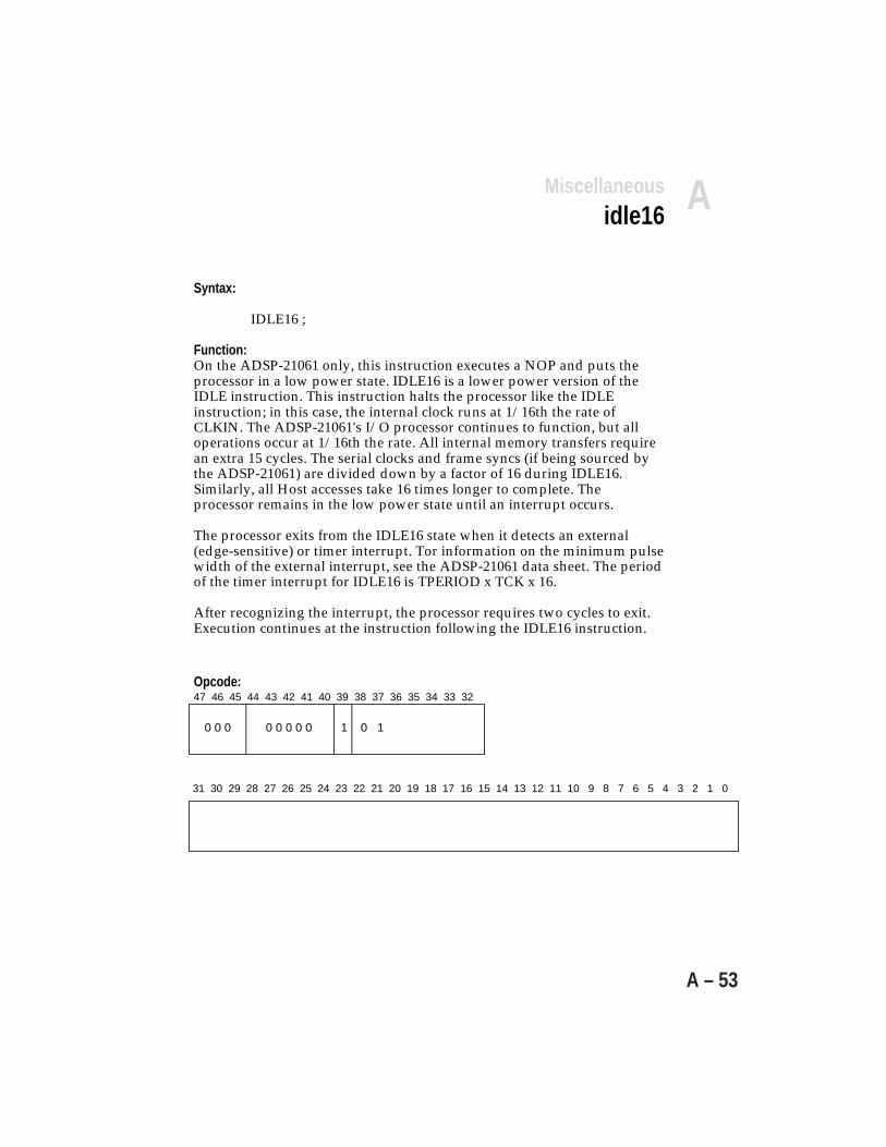
AInstruction Set Reference
A – 53
Miscellaneousidle16
Syntax:
IDLE16 ;
Function:On the ADSP-21061 only, this instruction executes a NOP and puts theprocessor in a low power state. IDLE16 is a lower power version of theIDLE instruction. This instruction halts the processor like the IDLEinstruction; in this case, the internal clock runs at 1/16th the rate ofCLKIN. The ADSP-21061's I/O processor continues to function, but alloperations occur at 1/16th the rate. All internal memory transfers requirean extra 15 cycles. The serial clocks and frame syncs (if being sourced bythe ADSP-21061) are divided down by a factor of 16 during IDLE16.Similarly, all Host accesses take 16 times longer to complete. Theprocessor remains in the low power state until an interrupt occurs.
The processor exits from the IDLE16 state when it detects an external(edge-sensitive) or timer interrupt. Tor information on the minimum pulsewidth of the external interrupt, see the ADSP-21061 data sheet. The periodof the timer interrupt for IDLE16 is TPERIOD x TCK x 16.
After recognizing the interrupt, the processor requires two cycles to exit.Execution continues at the instruction following the IDLE16 instruction.
Opcode:47 46 45 44 43 42 41 40 39 38 37 36 35 34 33 32
0 0 0 0 0 0 0 0 1 0 1
31 30 29 28 27 26 25 24 23 22 21 20 19 18 17 16 15 14 13 12 11 10 9 8 7 6 5 4 3 2 1 0
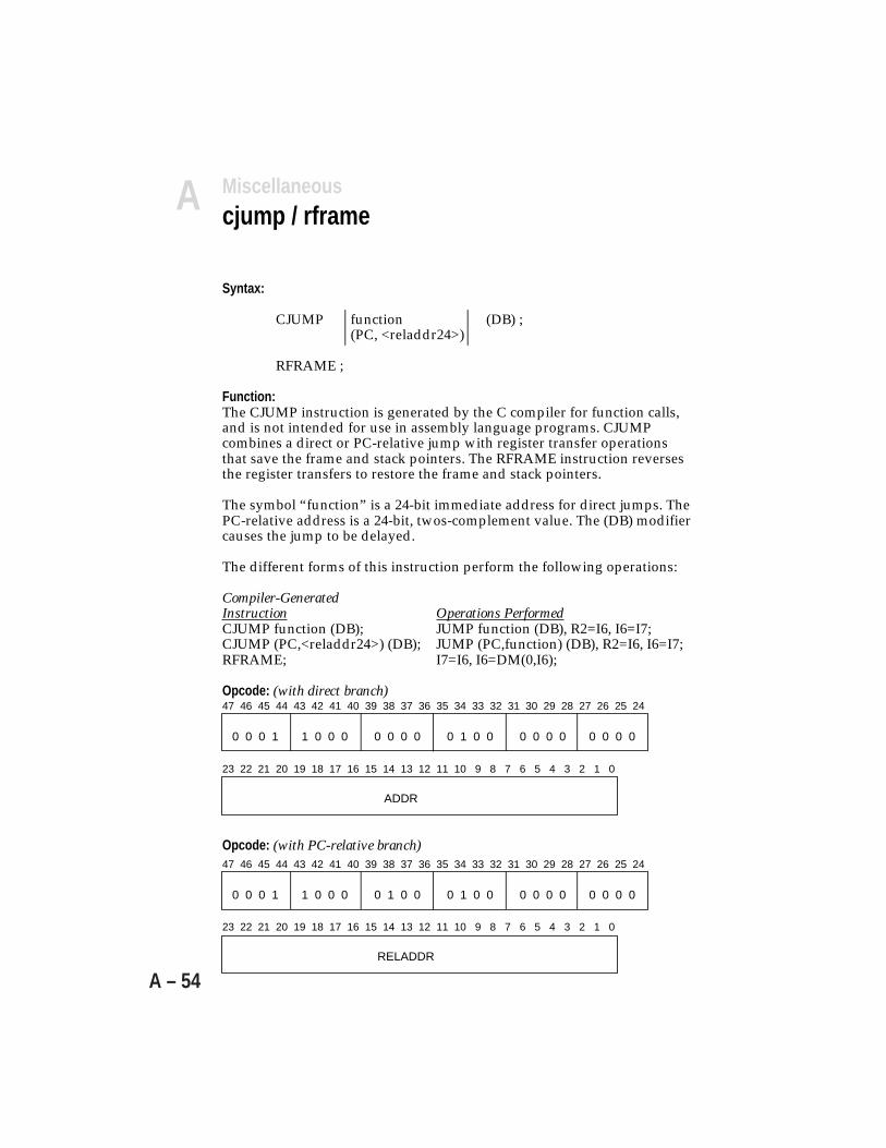
Instruction Set ReferenceA
A – 54
Syntax:
CJUMP function (DB) ;(PC, <reladdr24>)
RFRAME ;
Function:The CJUMP instruction is generated by the C compiler for function calls,and is not intended for use in assembly language programs. CJUMPcombines a direct or PC-relative jump with register transfer operationsthat save the frame and stack pointers. The RFRAME instruction reversesthe register transfers to restore the frame and stack pointers.
The symbol “function” is a 24-bit immediate address for direct jumps. ThePC-relative address is a 24-bit, twos-complement value. The (DB) modifiercauses the jump to be delayed.
The different forms of this instruction perform the following operations:
Compiler-GeneratedInstruction Operations PerformedCJUMP function (DB); JUMP function (DB), R2=I6, I6=I7;CJUMP (PC,<reladdr24>) (DB); JUMP (PC,function) (DB), R2=I6, I6=I7;RFRAME; I7=I6, I6=DM(0,I6);
Opcode: (with direct branch)47 46 45 44 43 42 41 40 39 38 37 36 35 34 33 32 31 30 29 28 27 26 25 24
0 0 0 1 1 0 0 0 0 0 0 0 0 1 0 0 0 0 0 0 0 0 0 0
23 22 21 20 19 18 17 16 15 14 13 12 11 10 9 8 7 6 5 4 3 2 1 0
ADDR
Opcode: (with PC-relative branch)47 46 45 44 43 42 41 40 39 38 37 36 35 34 33 32 31 30 29 28 27 26 25 24
0 0 0 1 1 0 0 0 0 1 0 0 0 1 0 0 0 0 0 0 0 0 0 0
23 22 21 20 19 18 17 16 15 14 13 12 11 10 9 8 7 6 5 4 3 2 1 0
RELADDR
Miscellaneouscjump / rframe

AInstruction Set Reference
A – 55
The ADDR field specifies a 24-bit program memory address for“function.” RELADDR is a 24-bit, twos-complement value that is added tothe current PC value to generate the branch address.
Opcode: (RFRAME)47 46 45 44 43 42 41 40 39 38 37 36 35 34 33 32 31 30 29 28 27 26 25 24
0 0 0 1 1 0 0 1 0 0 0 0 0 0 0 0 0 0 0 0 0 0 0 0
23 22 21 20 19 18 17 16 15 14 13 12 11 10 9 8 7 6 5 4 3 2 1 0
0 0 0 0 0 0 0 0 0 0 0 0 0 0 0 0 0 0 0 0 0 0 0 0
Miscellaneouscjump / rframe

Instruction Set ReferenceA
A – 56

BCompute OperationReference
B.1 OVERVIEWCompute operations execute in the multiplier, the ALU and the shifter.The 23-bit compute field is like a mini-instruction within the ADSP-21000instruction and can be specified for a variety of compute operations. Thisappendix describes each compute operation in detail, including itsassembly language syntax and opcode field.
A compute operation is one of the following:
• Single-function operations involve a single computation unit.
• Multifunction operations specify parallel operation of the multiplier andthe ALU or two operations in the ALU.
• The MR register transfer is a special type of compute operation used toaccess the fixed-point accumulator in the multiplier. (See p. B-52).
The operations in each category are described in the following sections.For each operation, the assembly language syntax, the function, and theopcode format and contents are specified. Refer to the beginning ofAppendix A for an explanation of the notation and abbreviations used.
B.2 SINGLE-FUNCTION OPERATIONSThe compute field of a single-function operation looks like:
22 21 20 19 18 17 16 15 14 13 12 11 10 9 8 7 6 5 4 3 2 1 0
0 CU OPCODE RN RX RY
An operation determined by OPCODE is executed in the computation unitspecified by CU. The x- and the y-operands are received from dataregisters RX and RY. The result operand is returned to data register RN.
B – 1
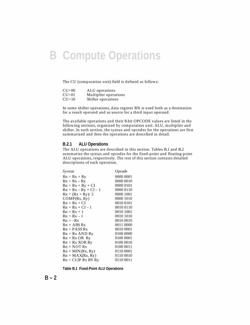
B Compute Operations
B – 2
The CU (computation unit) field is defined as follows:
CU=00 ALU operationsCU=01 Multiplier operationsCU=10 Shifter operations
In some shifter operations, data register RN is used both as a destinationfor a result operand and as source for a third input operand.
The available operations and their 8-bit OPCODE values are listed in thefollowing sections, organized by computation unit: ALU, multiplier andshifter. In each section, the syntax and opcodes for the operations are firstsummarized and then the operations are described in detail.
B.2.1 ALU OperationsThe ALU operations are described in this section. Tables B.1 and B.2summarize the syntax and opcodes for the fixed-point and floating-pointALU operations, respectively. The rest of this section contains detaileddescriptions of each operation.
Syntax OpcodeRn = Rx + Ry 0000 0001Rn = Rx – Ry 0000 0010Rn = Rx + Ry + CI 0000 0101Rn = Rx – Ry + CI – 1 0000 0110Rn = (Rx + Ry)/2 0000 1001COMP(Rx, Ry) 0000 1010Rn = Rx + CI 0010 0101Rn = Rx + CI – 1 0010 0110Rn = Rx + 1 0010 1001Rn = Rx – 1 0010 1010Rn = –Rx 0010 0010Rn = ABS Rx 0011 0000Rn = PASS Rx 0010 0001Rn = Rx AND Ry 0100 0000Rn = Rx OR Ry 0100 0001Rn = Rx XOR Ry 0100 0010Rn = NOT Rx 0100 0011Rn = MIN(Rx, Ry) 0110 0001Rn = MAX(Rx, Ry) 0110 0010Rn = CLIP Rx BY Ry 0110 0011
Table B.1 Fixed-Point ALU Operations

BCompute Operations
B – 3
Syntax OpcodeFn = Fx + Fy 1000 0001Fn = Fx – Fy 1000 0010Fn = ABS (Fx + Fy) 1001 0001Fn = ABS (Fx – Fy) 1001 0010Fn = (Fx + Fy)/2 1000 1001COMP(Fx, Fy) 1000 1010Fn = –Fx 1010 0010Fn = ABS Fx 1011 0000Fn = PASS Fx 1010 0001Fn = RND Fx 1010 0101Fn = SCALB Fx BY Ry 1011 1101Rn = MANT Fx 1010 1101Rn = LOGB Fx 1100 0001Rn = FIX Fx BY Ry 1101 1001Rn = FIX Fx 1100 1001Rn = TRUNC Fx BY Ry 1101 1101Rn = TRUNC Fx 1100 1101Fn = FLOAT Rx BY Ry 1101 1010Fn = FLOAT Rx 1100 1010Fn = RECIPS Fx 1100 0100Fn = RSQRTS Fx 1100 0101Fn = Fx COPYSIGN Fy 1110 0000Fn = MIN(Fx, Fy) 1110 0001Fn = MAX(Fx, Fy) 1110 0010Fn = CLIP Fx BY Fy 1110 0011
Table B.2 Floating-Point ALU Operations
The individual registers of the register file are prefixed with an “F”when used in floating-point computations. The registers are prefixedwith an “R” when used in fixed-point computations. The followinginstructions, for example, use the same registers:
F0=F1 * F2; floating-point multiplyR0=R1 * R2; fixed-point multiply
The F and R prefixes do not affect the 32-bit (or 40-bit) data transfer;they only determine how the ALU, multiplier, or shifter treat the data.The F and R may be either uppercase or lowercase; the assembler iscase-insensitive.
B Compute Operations
B – 4
Syntax:
Rn = Rx + Ry
Function:Adds the fixed-point fields in registers Rx and Ry. The result is placed inthe fixed-point field in register Rn. The floating-point extension field in Rnis set to all 0s. In saturation mode (the ALU saturation mode bit inMODE1 set) positive overflows return the maximum positive number(0x7FFF FFFF), and negative overflows return the minimum negativenumber (0x8000 0000).
Status flags:AZ Is set if the fixed-point output is all 0s, otherwise clearedAU Is clearedAN Is set if the most significant output bit is 1, otherwise clearedAV Is set if the XOR of the carries of the two most significant adder
stages is 1, otherwise clearedAC Is set if the carry from the most significant adder stage is 1,
otherwise clearedAS Is clearedAI Is cleared
ALU Fixed-PointRn = Rx + Ry

BCompute Operations
B – 5
Syntax:
Rn = Rx – Ry
Function:Subtracts the fixed-point field in register Ry from the fixed-point field inregister Rx. The result is placed in the fixed-point field in register Rn. Thefloating-point extension field in Rn is set to all 0s. In saturation mode (theALU saturation mode bit in MODE1 set) positive overflows return themaximum positive number (0x7FFF FFFF), and negative overflows returnthe minimum negative number (0x8000 0000).
Status flags:AZ Is set if the fixed-point output is all 0s, otherwise clearedAU Is clearedAN Is set if the most significant output bit is 1, otherwise clearedAV Is set if the XOR of the carries of the two most significant adder
stages is 1, otherwise clearedAC Is set if the carry from the most significant adder stage is 1,
otherwise clearedAS Is clearedAI Is cleared
ALU Fixed-PointRn = Rx – Ry

B Compute Operations
B – 6
ALU Fixed-PointRn = Rx + Ry + CI
Syntax:
Rn = Rx + Ry + CI
Function:Adds with carry (AC from ASTAT) the fixed-point fields in registers Rxand Ry. The result is placed in the fixed-point field in register Rn. Thefloating-point extension field in Rn is set to all 0s. In saturation mode (theALU saturation mode bit in MODE1 set) positive overflows return themaximum positive number (0x7FFF FFFF), and negative overflows returnthe minimum negative number (0x8000 0000).
Status flags:AZ Is set if the fixed-point output is all 0s, otherwise clearedAU Is clearedAN Is set if the most significant output bit is 1, otherwise clearedAV Is set if the XOR of the carries of the two most significant adder
stages is 1, otherwise clearedAC Is set if the carry from the most significant adder stage is 1,
otherwise clearedAS Is clearedAI Is cleared
BCompute Operations
B – 7
Syntax:
Rn = Rx – Ry + CI – 1
Function:Subtracts with borrow (AC – 1 from ASTAT) the fixed-point field inregister Ry from the fixed-point field in register Rx. The result is placed inthe fixed-point field in register Rn. The floating-point extension field in Rnis set to all 0s. In saturation mode (the ALU saturation mode bit inMODE1 set) positive overflows return the maximum positive number(0x7FFF FFFF), and negative overflows return the minimum negativenumber (0x8000 0000).
Status flags:AZ Is set if the fixed-point output is all 0s, otherwise clearedAU Is clearedAN Is set if the most significant output bit is 1, otherwise clearedAV Is set if the XOR of the carries of the two most significant adder
stages is 1, otherwise clearedAC Is set if the carry from the most significant adder stage is 1,
otherwise clearedAS Is clearedAI Is cleared
ALU Fixed-PointRn = Rx – Ry + CI – 1
B Compute Operations
B – 8
Syntax:
Rn = (Rx + Ry)/2
Function:Adds the fixed-point fields in registers Rx and Ry and divides the resultby 2. The result is placed in the fixed-point field in register Rn. Thefloating-point extension field in Rn is set to all 0s. Rounding is to nearest(IEEE) or by truncation, as defined by the rounding mode bit in theMODE1 register.
Status flags:AZ Is set if the fixed-point output is all 0s, otherwise clearedAU Is clearedAN Is set if the most significant output bit is 1, otherwise clearedAV Is clearedAC Is set if the carry from the most significant adder stage is 1,
otherwise clearedAS Is clearedAI Is cleared
ALU Fixed-PointRn = (Rx + Ry)/2
BCompute Operations
B – 9
Syntax:
COMP(Rx, Ry)
Function:Compares the fixed-point field in register Rx with the fixed-point field inregister Ry. Sets the AZ flag if the two operands are equal, and the ANflag if the operand in register Rx is smaller than the operand in registerRy.
The ASTAT register stores the results of the previous eight ALU compareoperations in bits 24-31. These bits are shifted right (bit 24 is overwritten)whenever a fixed-point or floating-point compare instruction is executed.The MSB of ASTAT is set if the X operand is greater than the Y operand(its value is the AND of ~AZ and ~AN); it is otherwise cleared.
Status flags:AZ Is set if the operands in registers Rx and Ry are equal, otherwise
clearedAU Is clearedAN Is set if the operand in the Rx register is smaller than the operand in
the Ry register, otherwise clearedAV Is clearedAC Is clearedAS Is clearedAI Is cleared
ALU Fixed-PointCOMP(Rx, Ry)
B Compute Operations
B – 10
Syntax:
Rn = Rx + CI
Function:Adds the fixed-point field in register Rx with the carry flag from theASTAT register (AC). The result is placed in the fixed-point field inregister Rn. The floating-point extension field in Rn is set to all 0s. Insaturation mode (the ALU saturation mode bit in MODE1 set) positiveoverflows return the maximum positive number (0x7FFF FFFF).
Status flags:AZ Is set if the fixed-point output is all 0s, otherwise clearedAU Is clearedAN Is set if the most significant output bit is 1, otherwise clearedAV Is set if the XOR of the carries of the two most significant adder
stages is 1, otherwise clearedAC Is set if the carry from the most significant adder stage is 1,
otherwise clearedAS Is clearedAI Is cleared
ALU Fixed-PointRn = Rx + CI
BCompute Operations
B – 11
Syntax:
Rn = Rx + CI – 1
Function:Adds the fixed-point field in register Rx with the borrow from the ASTATregister (AC – 1). The result is placed in the fixed-point field in register Rn.The floating-point extension field in Rn is set to all 0s. In saturation mode(the ALU saturation mode bit in MODE1 set) positive overflows return themaximum positive number (0x7FFF FFFF).
Status flags:AZ Is set if the fixed-point output is all 0s, otherwise clearedAU Is clearedAN Is set if the most significant output bit is 1, otherwise clearedAV Is set if the XOR of the carries of the two most significant adder
stages is 1, otherwise clearedAC Is set if the carry from the most significant adder stage is 1,
otherwise clearedAS Is clearedAI Is cleared
ALU Fixed-PointRn = Rx + CI – 1
B Compute Operations
B – 12
Syntax:
Rn = Rx + 1
Function:Increments the fixed-point operand in register Rx. The result is placed inthe fixed-point field in register Rn. The floating-point extension field in Rnis set to all 0s. In saturation mode (the ALU saturation mode bit inMODE1 set), overflow causes the maximum positive number(0x7FFF FFFF) to be returned.
Status flags:AZ Is set if the fixed-point output is all 0s, otherwise clearedAU Is clearedAN Is set if the most significant output bit is 1, otherwise clearedAV Is set if the XOR of the carries of the two most significant adder,
stages is 1, otherwise clearedAC Is set if the carry from the most significant adder stage is 1,
otherwise clearedAS Is clearedAI Is cleared
ALU Fixed-PointRn = Rx + 1
BCompute Operations
B – 13
Syntax:
Rn = Rx – 1
Function:Decrements the fixed-point operand in register Rx. The result is placed inthe fixed-point field in register Rn. The floating-point extension field in Rnis set to all 0s. In saturation mode (the ALU saturation mode bit inMODE1 set), underflow causes the minimum negative number(0x8000 0000) to be returned.
Status flags:AZ Is set if the fixed-point output is all 0s, otherwise clearedAU Is clearedAN Is set if the most significant output bit is 1, otherwise clearedAV Is set if the XOR of the carries of the two most significant adder
stages is 1, otherwise clearedAC Is set if the carry from the most significant adder stage is 1,
otherwise clearedAS Is clearedAI Is cleared
ALU Fixed-PointRn = Rx – 1
B Compute Operations
B – 14
ALU Fixed-PointRn = –Rx
Syntax:
Rn = –Rx
Function:Negates the fixed-point operand in Rx by twos complement. The result isplaced in the fixed-point field in register Rn. The floating-point extensionfield in Rn is set to all 0s. Negation of the minimum negative number(0x8000 0000) causes an overflow. In saturation mode (the ALU saturationmode bit in MODE1 set), overflow causes the maximum positive number(0x7FFF FFFF) to be returned.
Status flags:AZ Is set if the fixed-point output is all 0sAU Is clearedAN Is set if the most significant output bit is 1AV Is set if the XOR of the carries of the two most significant adder
stages is 1AC Is set if the carry from the most significant adder stage is 1,
otherwise clearedAS Is clearedAI Is cleared
BCompute Operations
B – 15
Syntax:
Rn = ABS Rx
Function:Determines the absolute value of the fixed-point operand in Rx. The resultis placed in the fixed-point field in register Rn. The floating-pointextension field in Rn is set to all 0s. ABS of the minimum negative number(0x8000 0000) causes an overflow. In saturation mode (the ALU saturationmode bit in MODE1 set), overflow causes the maximum positive number(0x7FFF FFFF) to be returned.
Status flags:AZ Is set if the fixed-point output is all 0s, otherwise clearedAU Is clearedAN Is set if the most significant output bit is 1, otherwise clearedAV Is set if the XOR of the carries of the two most significant adder
stages is 1, otherwise clearedAC Is set if the carry from the most significant adder stage is 1,
otherwise clearedAS Is set if the fixed-point operand in Rx is negative, otherwise clearedAI Is cleared
ALU Fixed-PointRn = ABS Rx
B Compute Operations
B – 16
Syntax:
Rn = PASS Rx
Function:Passes the fixed-point operand in Rx through the ALU to the fixed-pointfield in register Rn. The floating-point extension field in Rn is set to all 0s.
Status flags:AZ Is set if the fixed-point output is all 0s, otherwise clearedAU Is clearedAN Is set if the most significant output bit is 1, otherwise clearedAV Is clearedAC Is clearedAS Is clearedAI Is cleared
ALU Fixed-PointRn = PASS Rx
BCompute Operations
B – 17
Syntax:
Rn = Rx AND Ry
Function:Logically ANDs the fixed-point operands in Rx and Ry. The result isplaced in the fixed-point field in Rn. The floating-point extension field inRn is set to all 0s.
Status flags:AZ Is set if the fixed-point output is all 0s, otherwise clearedAU Is clearedAN Is set if the most significant output bit is 1, otherwise clearedAV Is clearedAC Is clearedAS Is clearedAI Is cleared
ALU Fixed-PointRn = Rx AND Ry
B Compute Operations
B – 18
Syntax:
Rn = Rx OR Ry
Function:Logically ORs the fixed-point operands in Rx and Ry. The result is placedin the fixed-point field in Rn. The floating-point extension field in Rn is setto all 0s.
Status flags:AZ Is set if the fixed-point output is all 0s, otherwise clearedAU Is clearedAN Is set if the most significant output bit is 1, otherwise clearedAV Is clearedAC Is clearedAS Is clearedAI Is cleared
ALU Fixed-PointRn = Rx OR Ry

BCompute Operations
B – 19
Syntax:
Rn = Rx XOR Ry
Function:Logically XORs the fixed-point operands in Rx and Ry. The result isplaced in the fixed-point field in Rn. The floating-point extension field inRn is set to all 0s.
Status flags:AZ Is set if the fixed-point output is all 0s, otherwise clearedAU Is clearedAN Is set if the most significant output bit is 1, otherwise clearedAV Is clearedAC Is clearedAS Is clearedAI Is cleared
ALU Fixed-PointRn = Rx XOR Ry
B Compute Operations
B – 20
Syntax:
Rn = NOT Rx
Function:Logically complements the fixed-point operand in Rx. The result is placedin the fixed-point field in Rn. The floating-point extension field in Rn is setto all 0s.
Status flags:AZ Is set if the fixed-point output is all 0s, otherwise clearedAU Is clearedAN Is set if the most significant output bit is 1, otherwise clearedAV Is clearedAC Is clearedAS Is clearedAI Is cleared
ALU Fixed-PointRn = NOT Rx

BCompute Operations
B – 21
Syntax:
Rn = MIN(Rx, Ry)
Function:Returns the smaller of the two fixed-point operands in Rx and Ry. Theresult is placed in the fixed-point field in register Rn. The floating-pointextension field in Rn is set to all 0s.
Status flags:AZ Is set if the fixed-point output is all 0s, otherwise clearedAU Is clearedAN Is set if the most significant output bit is 1, otherwise clearedAV Is clearedAC Is clearedAS Is clearedAI Is cleared
ALU Fixed-PointRn = MIN(Rx, Ry)
B Compute Operations
B – 22
Syntax:
Rn = MAX(Rx, Ry)
Function:Returns the larger of the two fixed-point operands in Rx and Ry. Theresult is placed in the fixed-point field in register Rn. The floating-pointextension field in Rn is set to all 0s.
Status flags:AZ Is set if the fixed-point output is all 0s, otherwise clearedAU Is clearedAN Is set if the most significant output bit is 1, otherwise clearedAV Is clearedAC Is clearedAS Is clearedAI Is cleared
ALU Fixed-PointRn = MAX(Rx, Ry)
BCompute Operations
B – 23
Syntax:
Rn = CLIP Rx BY Ry
Function:Returns the fixed-point operand in Rx if the absolute value of the operandin Rx is less than the absolute value of the fixed-point operand in Ry.Otherwise, returns |Ry| if Rx is positive, and –|Ry| if Rx is negative. Theresult is placed in the fixed-point field in register Rn. The floating-pointextension field in Rn is set to all 0s.
Status flags:AZ Is set if the fixed-point output is all 0s, otherwise clearedAU Is clearedAN Is set if the most significant output bit is 1, otherwise clearedAV Is clearedAC Is clearedAS Is clearedAI Is cleared
ALU Fixed-PointRn = CLIP Rx BY Ry

B Compute Operations
B – 24
Syntax:
Fn = Fx + Fy
Function:Adds the floating-point operands in registers Fx and Fy. The normalizedresult is placed in register Fn. Rounding is to nearest (IEEE) or bytruncation, to a 32-bit or to a 40-bit boundary, as defined by the roundingmode and rounding boundary bits in MODE1. Post-rounded overflowreturns ±Infinity (round-to-nearest) or ±NORM.MAX (round-to-zero).Post-rounded denormal returns ±Zero. Denormal inputs are flushed to±Zero. A NAN input returns an all 1s result.
Status flags:AZ Is set if the post-rounded result is a denormal
(unbiased exponent < –126) or zero, otherwise clearedAU Is set if the post-rounded result is a denormal, otherwise clearedAN Is set if the floating-point result is negative, otherwise clearedAV Is set if the post-rounded result overflows
(unbiased exponent > +127), otherwise clearedAC Is clearedAS Is clearedAI Is set if either of the input operands is a NAN, or if they are
opposite-signed Infinities, otherwise cleared
ALU Floating-PointFn = Fx + Fy

BCompute Operations
B – 25
Syntax:
Fn = Fx – Fy
Function:Subtracts the floating-point operand in register Fy from the floating-pointoperand in register Fx. The normalized result is placed in register Fn.Rounding is to nearest (IEEE) or by truncation, to a 32-bit or to a 40-bitboundary, as defined by the rounding mode and rounding boundary bitsin MODE1. Post-rounded overflow returns ±Infinity (round-to-nearest) or±NORM.MAX (round-to-zero). Post-rounded denormal returns ±Zero.Denormal inputs are flushed to ±Zero. A NAN input returns an all 1sresult.
Status flags:AZ Is set if the post-rounded result is a denormal
(unbiased exponent < –126) or zero, otherwise clearedAU Is set if the post-rounded result is a denormal, otherwise clearedAN Is set if the floating-point result is negative, otherwise clearedAV Is set if the post-rounded result overflows
(unbiased exponent > +127), otherwise clearedAC Is clearedAS Is clearedAI Is set if either of the input operands is a NAN, or if they are like-
signed Infinities, otherwise cleared
ALU Floating-PointFn = Fx – Fy
B Compute Operations
B – 26
Syntax:
Fn = ABS (Fx + Fy)
Function:Adds the floating-point operands in registers Fx and Fy, and places theabsolute value of the normalized result in register Fn. Rounding is tonearest (IEEE) or by truncation, to a 32-bit or to a 40-bit boundary, asdefined by the rounding mode and rounding boundary bits in MODE1.Post-rounded overflow returns +Infinity (round-to-nearest) or+NORM.MAX (round-to-zero). Post-rounded denormal returns +Zero.Denormal inputs are flushed to ±Zero. A NAN input returns an all 1sresult.
Status flags:AZ Is set if the post-rounded result is a denormal
(unbiased exponent < –126) or zero, otherwise clearedAU Is set if the post-rounded result is a denormal, otherwise clearedAN Is clearedAV Is set if the post-rounded result overflows
(unbiased exponent > +127), otherwise clearedAC Is clearedAS Is clearedAI Is set if either of the input operands is a NAN, or if they are
opposite-signed Infinities, otherwise cleared
ALU Floating-PointFn = ABS (Fx + Fy)
BCompute Operations
B – 27
Syntax:
Fn = ABS (Fx – Fy)
Function:Subtracts the floating-point operand in Fy from the floating-point operandin Fx and places the absolute value of the normalized result in register Fn.Rounding is to nearest (IEEE) or by truncation, to a 32-bit or to a 40-bitboundary, as defined by the rounding mode and rounding boundary bitsin MODE1. Post-rounded overflow returns +Infinity (round-to-nearest) or+NORM.MAX (round-to-zero). Post-rounded denormal returns +Zero.Denormal inputs are flushed to ±Zero. A NAN input returns an all 1sresult.
Status flags:AZ Is set if the post-rounded result is a denormal
(unbiased exponent < –126) or zero, otherwise clearedAU Is set if the post-rounded result is a denormal, otherwise clearedAN Is clearedAV Is set if the post-rounded result overflows
(unbiased exponent > +127), otherwise clearedAC Is clearedAS Is clearedAI Is set if either of the input operands is a NAN, or if they are like-
signed Infinities, otherwise cleared
ALU Floating-PointFn = ABS (Fx – Fy)
B Compute Operations
B – 28
Syntax:
Fn = (Fx + Fy)/2
Function:Adds the floating-point operands in registers Fx and Fy and divides theresult by 2, by decrementing the exponent of the sum before rounding.The normalized result is placed in register Fn. Rounding is to nearest(IEEE) or by truncation, to a 32-bit or to a 40-bit boundary, as defined bythe rounding mode and rounding boundary bits in MODE1. Post-roundedoverflow returns ±Infinity (round-to-nearest) or ±NORM.MAX (round-to-zero). Post-rounded denormal results return ±Zero. A denormal input isflushed to ±Zero. A NAN input returns an all 1s result.
Status flags:AZ Is set if the post-rounded result is a denormal
(unbiased exponent < –126) or zero, otherwise clearedAU Is set if the post-rounded result is a denormal, otherwise clearedAN Is set if the floating-point result is negative, otherwise clearedAV Is set if the post-rounded result overflows
(unbiased exponent > +127), otherwise clearedAC Is clearedAS Is clearedAI Is set if either of the input operands is a NAN, or if they are
opposite-signed Infinities, otherwise cleared
ALU Floating-PointFn = (Fx + Fy)/2

BCompute Operations
B – 29
Syntax:
COMP(Fx, Fy)
Function:Compares the floating-point operand in register Fx with the floating-pointoperand in register Fy. Sets the AZ flag if the two operands are equal, andthe AN flag if the operand in register Fx is smaller than the operand inregister Fy.
The ASTAT register stores the results of the previous eight ALU compareoperations in bits 24-31. These bits are shifted right (bit 24 is overwritten)whenever a fixed-point or floating-point compare instruction is executed.The MSB of ASTAT is set if the X operand is greater than the Y operand(its value is the AND of ~AZ and ~AN); it is otherwise cleared.
Status flags:AZ Is set if the operands in registers Fx and Fy are equal, otherwise
clearedAU Is clearedAN Is set if the operand in the Fx register is smaller than the operand in
the Fy register, otherwise clearedAV Is clearedAC Is clearedAS Is clearedAI Is set if either of the input operands is a NAN, otherwise cleared
ALU Floating-PointCOMP(Fx, Fy)
B Compute Operations
B – 30
Syntax:
Fn = –Fx
Function:Complements the sign bit of the floating-point operand in Fx. Thecomplemented result is placed in register Fn. A denormal input is flushedto ±Zero. A NAN input returns an all 1s result.
Status flags:AZ Is set if the result operand is a ±Zero, otherwise clearedAU Is clearedAN Is set if the floating-point result is negative, otherwise clearedAV Is clearedAC Is clearedAS Is clearedAI Is set if the input operand is a NAN, otherwise cleared
ALU Floating-PointFn = –Fx
BCompute Operations
B – 31
Syntax:
Fn = ABS Fx
Function:Returns the absolute value of the floating-point operand in register Fx bysetting the sign bit of the operand to 0. Denormal inputs are flushed to+Zero. A NAN input returns an all 1s result.
Status flags:AZ Is set if the result operand is +Zero, otherwise cleared.AU Is clearedAN Is clearedAV Is clearedAC Is clearedAS Is set if the input operand is negative, otherwise clearedAI Is set if the input operand is a NAN, otherwise cleared
ALU Floating-PointFn = ABS Fx
B Compute Operations
B – 32
Syntax:
Fn = PASS Fx
Function:Passes the floating-point operand in Fx through the ALU to the floating-point field in register Fn. Denormal inputs are flushed to ±Zero. A NANinput returns an all 1s result.
Status flags:AZ Is set if the result operand is a ±Zero, otherwise clearedAU Is clearedAN Is set if the floating-point result is negative, otherwise clearedAV Is clearedAC Is clearedAS Is clearedAI Is set if the input operand is a NAN, otherwise cleared
ALU Floating-PointFn = PASS Fx
BCompute Operations
B – 33
Syntax:
Fn = RND Fx
Function:Rounds the floating-point operand in register Fx to a 32 bit boundary.Rounding is to nearest (IEEE) or by truncation, as defined by the roundingmode bit in MODE1. Post-rounded overflow returns ±Infinity (round-to-nearest) or ±NORM.MAX (round-to-zero). A denormal input is flushed to±Zero. A NAN input returns an all 1s result.
Status flags:AZ Is set if the result operand is a ±Zero, otherwise clearedAU Is clearedAN Is set if the floating-point result is negative, otherwise clearedAV Is set if the post-rounded result overflows
(unbiased exponent > +127), otherwise clearedAC Is clearedAS Is clearedAI Is set if the input operand is a NAN, otherwise cleared
ALU Floating-PointFn = RND Fx
B Compute Operations
B – 34
Syntax:
Fn = SCALB Fx BY Ry
Function:Scales the exponent of the floating-point operand in Fx by adding to it thefixed-point twos-complement integer in Ry. The scaled floating-pointresult is placed in register Fn. Overflow returns ±Infinity (round-to-nearest) or ±NORM.MAX (round-to-zero). Denormal returns ±Zero.Denormal inputs are flushed to ±Zero. A NAN input returns an all 1sresult.
Status flags:AZ Is set if the result is a denormal (unbiased exponent < –126) or zero,
otherwise clearedAU Is set if the post-rounded result is a denormal, otherwise clearedAN Is set if the floating-point result is negative, otherwise clearedAV Is set if the result overflows (unbiased exponent > +127), otherwise
clearedAC Is clearedAS Is clearedAI Is set if the input is a NAN, an otherwise cleared
ALU Floating-PointFn = SCALB Fx BY Ry
BCompute Operations
B – 35
Syntax:
Rn = MANT Fx
Function:Extracts the mantissa (fraction bits with explicit hidden bit, excluding thesign bit) from the floating-point operand in Fx. The unsigned-magnituderesult is left-justified (1.31 format) in the fixed-point field in Rn. Roundingmodes are ignored and no rounding is performed because all results areinherently exact. Denormal inputs are flushed to ±Zero. A NAN or anInfinity input returns an all 1s result (–1 in signed fixed-point format).
Status flags:AZ Is set if the result is zero, otherwise clearedAU Is clearedAN Is clearedAV Is clearedAC Is clearedAS Is set if the input is negative, otherwise clearedAI Is set if the input operands is a NAN or an Infinity, otherwise
cleared
ALU Floating-PointRn = MANT Fx
B Compute Operations
B – 36
Syntax:
Rn = LOGB Fx
Function:Converts the exponent of the floating-point operand in register Fx to anunbiased twos-complement fixed-point integer. The result is placed in thefixed-point field in register Rn. Unbiasing is done by subtracting 127 fromthe floating-point exponent in Fx. If saturation mode is not set, a ±Infinityinput returns a floating-point +Infinity and a ±Zero input returns afloating-point –Infinity. If saturation mode is set, a ±Infinity input returnsthe maximum positive value (0x7FFF FFFF) and a ±Zero input returns themaximum negative value (0x8000 0000). Denormal inputs are flushed to±Zero. A NAN input returns an all 1s result.
Status flags:AZ Is set if the fixed-point result is zero, otherwise clearedAU Is clearedAN Is set if the result is negative, otherwise clearedAV Is set if the input operand is an Infinity or a Zero, otherwise clearedAC Is clearedAS Is clearedAI Is set if the input is a NAN, otherwise cleared
ALU Floating-PointRn = LOGB Fx
BCompute Operations
B – 37
Syntax:
Rn = FIX Fx Rn = TRUNC FxRn = FIX Fx BY Ry Rn = TRUNC Fx BY Ry
Function:Converts the floating-point operand in Fx to a twos-complement 32-bitfixed-point integer result. If the MODE1 register TRUNC bit=1, the FIXoperation truncates the mantissa towards –Infinity. If the TRUNC bit=0,the FIX operation rounds the mantissa towards the nearest integer. TheTRUNC operation always truncates toward 0. Note that the TRUNC bitdoes not influence operation of the TRUNC instruction.
If a scaling factor (Ry) is specified, the fixed-point twos-complementinteger in Ry is added to the exponent of the floating-point operand in Fxbefore the conversion. The result of the conversion is right-justified (32.0format) in the fixed-point field in register Rn. The floating-point extensionfield in Rn is set to all 0s. In saturation mode (the ALU saturation mode bitin MODE1 set) positive overflows and +Infinity return the maximumpositive number (0x7FFF FFFF), and negative overflows and –Infinityreturn the minimum negative number (0x8000 0000).
For the FIX operation, rounding is to nearest (IEEE) or by truncation, asdefined by the rounding mode bit in MODE1. A NAN input returns afloating-point all 1s result. If saturation mode is not set, an Infinity inputor a result that overflows returns a floating-point all 1s result. All positiveunderflows return zero. Negative underflows that are rounded-to-nearestreturn zero, and negative underflows that are rounded by truncationreturn –1 (0xFF FFFF FF00).
Status flags:AZ Is set if the fixed-point result is Zero, otherwise clearedAU Is set if the pre-rounded result is a denormal, otherwise clearedAN Is set if the fixed-point result is negative, otherwise clearedAV Is set if the conversion causes the floating-point mantissa to be
shifted left, i.e. if the floating-point exponent + scale bias is> 157 (127 + 31 – 1) or if the input is ±Infinity, otherwise cleared
AC Is clearedAS Is clearedAI Is set if the input operand is a NAN or, when saturation mode is not
set, either input is an Infinity or the result overflows, otherwisecleared
ALU Floating-PointRn = FIX Fx
Rn = TRUNC Fx
B Compute Operations
B – 38
Syntax:
Fn = FLOAT Rx BY RyFn = FLOAT Rx
Function:Converts the fixed-point operand in Rx to a floating-point result. If ascaling factor (Ry) is specified, the fixed-point twos-complement integer inRy is added to the exponent of the floating-point result. The final result isplaced in register Fn.
Rounding is to nearest (IEEE) or by truncation, as defined by the roundingmode, to a 40-bit boundary, regardless of the values of the roundingboundary bits in MODE1. The exponent scale bias may cause a floating-point overflow or a floating-point underflow. Overflow causes a ±Infinity(round-to-nearest) or ±NORM.MAX (round-to-zero) to be returned;underflow causes a ±Zero to be returned.
Status flags:AZ Is set if the result is a denormal (unbiased exponent < –126) or zero,
otherwise clearedAU Is set if the post-rounded result is a denormal, otherwise clearedAN Is set if the floating-point result is negative, otherwise clearedAV Is set if the result overflows (unbiased exponent >127)AC Is clearedAS Is clearedAI Is cleared
ALU Floating-PointFn = FLOAT Rx BY Ry / Fn = FLOAT Rx

BCompute Operations
B – 39
Syntax:
Fn = RECIPS Fx
Function:Creates an 8-bit accurate seed for 1/Fx, the reciprocal of Fx. The mantissaof the seed is determined from a ROM table using the 7 MSBs (excludingthe hidden bit) of the Fx mantissa as an index. The unbiased exponent ofthe seed is calculated as the twos complement of the unbiased Fxexponent, decremented by one; i.e., if e is the unbiased exponent of Fx,then the unbiased exponent of Fn = –e – 1. The sign of the seed is the signof the input. ±Zero returns ±Infinity and sets the overflow flag. If theunbiased exponent of Fx is greater than +125, the result is ±Zero. A NANinput returns an all 1s result.
The following code performs floating-point division using an iterativeconvergence algorithm.* The result is accurate to one LSB in whicheverformat mode, 32-bit or 40-bit, is set (32-bit only for ADSP-21010). Thefollowing inputs are required: F0=numerator, F12=denominator, F11=2.0.The quotient is returned in F0. (The two highlighted instructions can beremoved if only a ±1 LSB accurate single-precision result is necessary.)
F0=RECIPS F12, F7=F0; Get 8 bit seed R0=1/DF12=F0*F12; D' = D*R0F7=F0*F7, F0=F11-F12; F0=R1=2-D', F7=N*R0F12=F0*F12; F12=D'-D'*R1F7=F0*F7, F0=F11-F12; F7=N*R0*R1, F0=R2=2-D'
F12=F0*F12; F12=D'=D'*R2 F7=F0*F7, F0=F11-F12; F7=N*R0*R1*R2, F0=R3=2-D'
F0=F0*F7; F7=N*R0*R1*R2*R3
Note that this code segment can be made into a subroutine by adding anRTS(DB) clause to the third-to-last instruction.
Status flags:AZ Is set if the floating-point result is ±Zero (unbiased exponent of Fx is
greater than +125), otherwise clearedAU Is clearedAN Is set if the input operand is negative, otherwise clearedAV Is set if the input operand is ±Zero, otherwise clearedAC Is clearedAS Is clearedAI Is set if the input operand is a NAN, otherwise cleared
* Cavanagh, J. 1984. Digital Computer Arithmetic. McGraw-Hill. Page 284.
ALU Floating-PointFn = RECIPS Fx
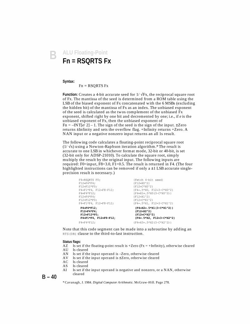
B Compute Operations
B – 40
Syntax:Fn = RSQRTS Fx
Function: Creates a 4-bit accurate seed for 1/√Fx, the reciprocal square rootof Fx. The mantissa of the seed is determined from a ROM table using theLSB of the biased exponent of Fx concatenated with the 6 MSBs (excludingthe hidden bit) of the mantissa of Fx as an index. The unbiased exponentof the seed is calculated as the twos complement of the unbiased Fxexponent, shifted right by one bit and decremented by one; i.e., if e is theunbiased exponent of Fx, then the unbiased exponent ofFn = –INT[e/2] – 1. The sign of the seed is the sign of the input. ±Zeroreturns ±Infinity and sets the overflow flag. +Infinity returns +Zero. ANAN input or a negative nonzero input returns an all 1s result.
The following code calculates a floating-point reciprocal square root(1/√x) using a Newton-Raphson iteration algorithm.* The result isaccurate to one LSB in whichever format mode, 32-bit or 40-bit, is set(32-bit only for ADSP-21010). To calculate the square root, simplymultiply the result by the original input. The following inputs arerequired: F0=input, F8=3.0, F1=0.5. The result is returned in F4. (The fourhighlighted instructions can be removed if only a ±1 LSB accurate single-precision result is necessary.)
F4=RSQRTS F0; Fetch 4-bit seedF12=F4*F4; F12=X0^2F12=F12*F0; F12=C*X0^2F4=F1*F4, F12=F8-F12; F4=.5*X0, F12=3-C*X0^2F4=F4*F12; F4=X1=.5*X0(3-C*X0^2)F12=F4*F4; F12=X1^2F12=F12*F0; F12=C*X1^2F4=F1*F4, F12=F8-F12; F4=.5*X1, F12=3-C*X1^2
F4=F4*F12; F4=X2=.5*X1(3-C*X1^2) F12=F4*F4; F12=X2^2 F12=F12*F0; F12=C*X2^2 F4=F1*F4, F12=F8-F12; F4=.5*X2, F12=3-C*X2^2
F4=F4*F12; F4=X3=.5*X2(3-C*X2^2)
Note that this code segment can be made into a subroutine by adding anRTS(DB) clause to the third-to-last instruction.
Status flags:AZ Is set if the floating-point result is +Zero (Fx = +Infinity), otherwise clearedAU Is clearedAN Is set if the input operand is –Zero, otherwise clearedAV Is set if the input operand is ±Zero, otherwise clearedAC Is clearedAS Is clearedAI Is set if the input operand is negative and nonzero, or a NAN, otherwise
cleared
* Cavanagh, J. 1984. Digital Computer Arithmetic. McGraw-Hill. Page 278.
ALU Floating-PointFn = RSQRTS Fx

BCompute Operations
B – 41
Syntax:
Fn = Fx COPYSIGN Fy
Function:Copies the sign of the floating-point operand in register Fy to the floating-point operand from register Fx without changing the exponent or themantissa. The result is placed in register Fn. A denormal input is flushedto ±Zero. A NAN input returns an all 1s result.
Status flags:AZ Is set if the floating-point result is ±Zero, otherwise clearedAU Is clearedAN Is set if the floating-point result is negative, otherwise clearedAV Is clearedAC Is clearedAS Is clearedAI Is set if either of the input operands is a NAN, otherwise cleared
ALU Floating-PointFn = Fx COPYSIGN Fy

B Compute Operations
B – 42
Syntax:
Fn = MIN(Fx, Fy)
Function:Returns the smaller of the floating-point operands in register Fx and Fy. ANAN input returns an all 1s result. MIN of +Zero and –Zero returns–Zero. Denormal inputs are flushed to ±Zero.
Status flags:AZ Is set if the floating-point result is ±Zero, otherwise cleared.AU Is clearedAN Is set if the floating-point result is negative, otherwise clearedAV Is clearedAC Is clearedAS Is clearedAI Is set if either of the input operands is a NAN, otherwise cleared
ALU Floating-PointFn = MIN(Fx, Fy)
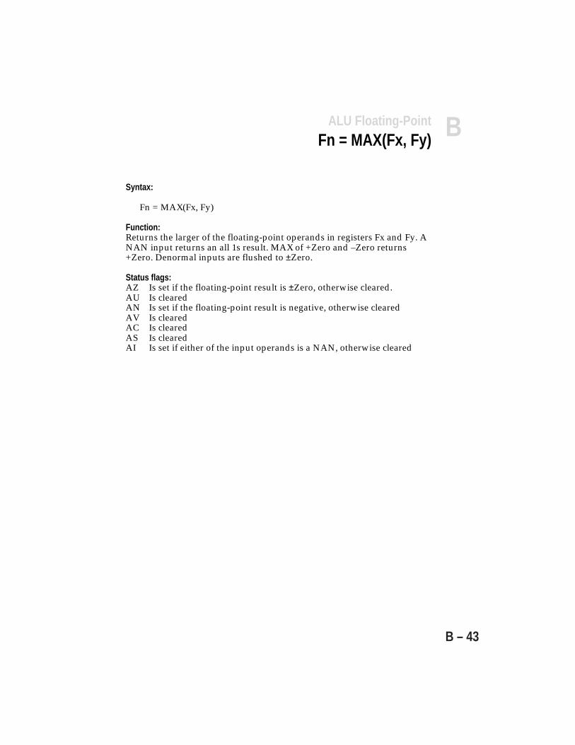
BCompute Operations
B – 43
Syntax:
Fn = MAX(Fx, Fy)
Function:Returns the larger of the floating-point operands in registers Fx and Fy. ANAN input returns an all 1s result. MAX of +Zero and –Zero returns+Zero. Denormal inputs are flushed to ±Zero.
Status flags:AZ Is set if the floating-point result is ±Zero, otherwise cleared.AU Is clearedAN Is set if the floating-point result is negative, otherwise clearedAV Is clearedAC Is clearedAS Is clearedAI Is set if either of the input operands is a NAN, otherwise cleared
ALU Floating-PointFn = MAX(Fx, Fy)
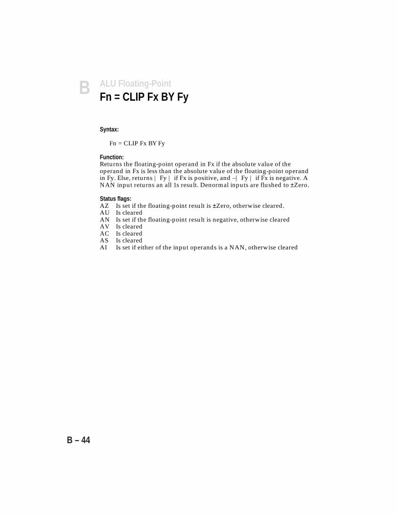
B Compute Operations
B – 44
Syntax:
Fn = CLIP Fx BY Fy
Function:Returns the floating-point operand in Fx if the absolute value of theoperand in Fx is less than the absolute value of the floating-point operandin Fy. Else, returns | Fy | if Fx is positive, and –| Fy | if Fx is negative. ANAN input returns an all 1s result. Denormal inputs are flushed to ±Zero.
Status flags:AZ Is set if the floating-point result is ±Zero, otherwise cleared.AU Is clearedAN Is set if the floating-point result is negative, otherwise clearedAV Is clearedAC Is clearedAS Is clearedAI Is set if either of the input operands is a NAN, otherwise cleared
ALU Floating-PointFn = CLIP Fx BY Fy
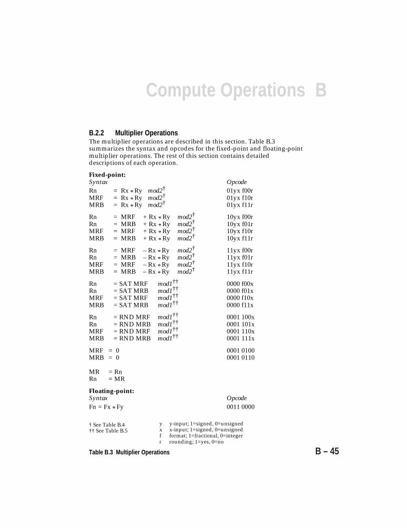
BCompute Operations
B – 45
B.2.2 Multiplier OperationsThe multiplier operations are described in this section. Table B.3summarizes the syntax and opcodes for the fixed-point and floating-pointmultiplier operations. The rest of this section contains detaileddescriptions of each operation.
Fixed-point:Syntax OpcodeRn = Rx * Ry mod2† 01yx f00rMRF = Rx * Ry mod2† 01yx f10rMRB = Rx * Ry mod2† 01yx f11r
Rn = MRF + Rx * Ry mod2† 10yx f00rRn = MRB + Rx * Ry mod2† 10yx f01rMRF = MRF + Rx * Ry mod2† 10yx f10rMRB = MRB + Rx * Ry mod2† 10yx f11r
Rn = MRF – Rx * Ry mod2† 11yx f00rRn = MRB – Rx * Ry mod2† 11yx f01rMRF = MRF – Rx * Ry mod2† 11yx f10rMRB = MRB – Rx * Ry mod2† 11yx f11r
Rn = SAT MRF mod1†† 0000 f00xRn = SAT MRB mod1†† 0000 f01xMRF = SAT MRF mod1†† 0000 f10xMRB = SAT MRB mod1†† 0000 f11x
Rn = RND MRF mod1†† 0001 100xRn = RND MRB mod1†† 0001 101xMRF = RND MRF mod1†† 0001 110xMRB = RND MRB mod1†† 0001 111x
MRF = 0 0001 0100MRB = 0 0001 0110
MR = RnRn = MR
Floating-point:Syntax OpcodeFn = Fx * Fy 0011 0000
† See Table B.4†† See Table B.5
y y-input; 1=signed, 0=unsignedx x-input; 1=signed, 0=unsignedf format; 1=fractional, 0=integerr rounding; 1=yes, 0=no
Table B.3 Multiplier Operations

B Compute Operations
B – 46
Mod2 in Table B.3 is an optional modifier, enclosed in parentheses,consisting of three or four letters that indicate whether the x-input issigned (S) or unsigned (U), whether the y-input is signed or unsigned,whether the inputs are in integer (I) or fractional (F) format and whetherthe result when written to the register file is to be rounded-to-nearest (R).The options for mod2 and the corresponding opcode values are listed inTable B.4.
Mod2 Opcode(SSI) --11 0--0(SUI) --01 0--0(USI) --10 0--0(UUI) --00 0--0(SSF) --11 1--0(SUF) --01 1--0(USF) --10 1--0(UUF) --00 1--0(SSFR) --11 1--1(SUFR) --01 1--1(USFR) --10 1--1(UUFR) --00 1--1
Table B.4 Multiplier Mod2 Options
Similarly, mod1 in Table B.3 is an optional modifier, enclosed inparentheses, consisting of two letters that indicate whether the input issigned (S) or unsigned (U) and whether the input is in integer (I) orfractional (F) format. The options for mod1 and the corresponding opcodevalues are listed in Table B.5.
Mod1 Opcode(SI) (for SAT only) ---- 0--1(UI) (for SAT only) ---- 0--0(SF) ---- 1--1(UF) ---- 1--0
Table B.5 Multiplier Mod1 Options
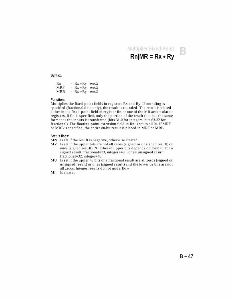
BCompute Operations
B – 47
Syntax:
Rn = Rx * Ry mod2MRF = Rx * Ry mod2MRB = Rx * Ry mod2
Function:Multiplies the fixed-point fields in registers Rx and Ry. If rounding isspecified (fractional data only), the result is rounded. The result is placedeither in the fixed-point field in register Rn or one of the MR accumulationregisters. If Rn is specified, only the portion of the result that has the sameformat as the inputs is transferred (bits 31-0 for integers, bits 63-32 forfractional). The floating-point extension field in Rn is set to all 0s. If MRFor MRB is specified, the entire 80-bit result is placed in MRF or MRB.
Status flags:MN Is set if the result is negative, otherwise clearedMV Is set if the upper bits are not all zeros (signed or unsigned result) or
ones (signed result). Number of upper bits depends on format. For asigned result, fractional=33, integer=49. For an unsigned result,fractional=32, integer=48.
MU Is set if the upper 48 bits of a fractional result are all zeros (signed orunsigned result) or ones (signed result) and the lower 32 bits are notall zeros. Integer results do not underflow.
MI Is cleared
Multiplier Fixed-PointRn|MR = Rx * Ry

B Compute Operations
B – 48
Syntax:
Rn = MRF + Rx * Ry mod2Rn = MRB + Rx * Ry mod2MRF = MRF + Rx * Ry mod2MRB = MRB + Rx * Ry mod2
Function:Multiplies the fixed-point fields in registers Rx and Ry, and adds theproduct to the specified MR register value. If rounding is specified(fractional data only), the result is rounded. The result is placed either inthe fixed-point field in register Rn or one of the MR accumulationregisters, which must be the same MR register that provided the input. IfRn is specified, only the portion of the result that has the same format asthe inputs is transferred (bits 31-0 for integers, bits 63-32 for fractional).The floating-point extension field in Rn is set to all 0s. If MRF or MRB isspecified, the entire 80-bit result is placed in MRF or MRB.
Status flags:MN Is set if the result is negative, otherwise clearedMV Is set if the upper bits are not all zeros (signed or unsigned result) or
ones (signed result). Number of upper bits depends on format. For asigned result, fractional=33, integer=49. For an unsigned result,fractional=32, integer=48.
MU Is set if the upper 48 bits of a fractional result are all zeros (signed orunsigned result) or ones (signed result) and the lower 32 bits are notall zeros. Integer results do not underflow.
MI Is cleared
Multiplier Fixed-PointRn|MR = MR + Rx * Ry

BCompute Operations
B – 49
Syntax:
Rn = MRF – Rx * Ry mod2Rn = MRB – Rx * Ry mod2MRF = MRF – Rx * Ry mod2MRB = MRB – Rx * Ry mod2
Function:Multiplies the fixed-point fields in registers Rx and Ry, and subtracts theproduct from the specified MR register value. If rounding is specified(fractional data only), the result is rounded. The result is placed either inthe fixed-point field in register Rn or one of the MR accumulationregisters, which must be the same MR register that provided the input. IfRn is specified, only the portion of the result that has the same format asthe inputs is transferred (bits 31-0 for integers, bits 63-32 for fractional).The floating-point extension field in Rn is set to all 0s. If MRF or MRB isspecified, the entire 80-bit result is placed in MRF or MRB.
Status flags:MN Is set if the result is negative, otherwise clearedMV Is set if the upper bits are not all zeros (signed or unsigned result) or
ones (signed result). Number of upper bits depends on format. For asigned result, fractional=33, integer=49. For an unsigned result,fractional=32, integer=48.
MU Is set if the upper 48 bits of a fractional result are all zeros (signed orunsigned result) or ones (signed result) and the lower 32 bits are notall zeros. Integer results do not underflow.
MI Is cleared
Multiplier Fixed-PointRn|MR = MR – Rx * Ry
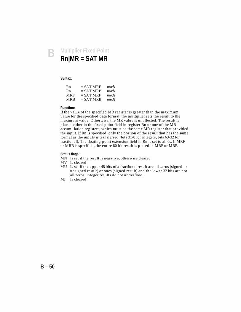
B Compute Operations
B – 50
Syntax:
Rn = SAT MRF mod1Rn = SAT MRB mod1MRF = SAT MRF mod1MRB = SAT MRB mod1
Function:If the value of the specified MR register is greater than the maximumvalue for the specified data format, the multiplier sets the result to themaximum value. Otherwise, the MR value is unaffected. The result isplaced either in the fixed-point field in register Rn or one of the MRaccumulation registers, which must be the same MR register that providedthe input. If Rn is specified, only the portion of the result that has the sameformat as the inputs is transferred (bits 31-0 for integers, bits 63-32 forfractional). The floating-point extension field in Rn is set to all 0s. If MRFor MRB is specified, the entire 80-bit result is placed in MRF or MRB.
Status flags:MN Is set if the result is negative, otherwise clearedMV Is clearedMU Is set if the upper 48 bits of a fractional result are all zeros (signed or
unsigned result) or ones (signed result) and the lower 32 bits are notall zeros. Integer results do not underflow.
MI Is cleared
Multiplier Fixed-PointRn|MR = SAT MR
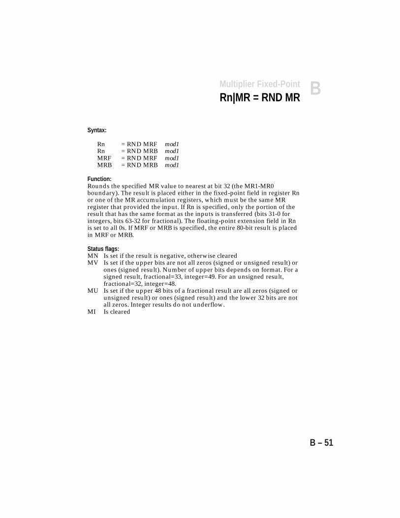
BCompute Operations
B – 51
Syntax:
Rn = RND MRF mod1Rn = RND MRB mod1MRF = RND MRF mod1MRB = RND MRB mod1
Function:Rounds the specified MR value to nearest at bit 32 (the MR1-MR0boundary). The result is placed either in the fixed-point field in register Rnor one of the MR accumulation registers, which must be the same MRregister that provided the input. If Rn is specified, only the portion of theresult that has the same format as the inputs is transferred (bits 31-0 forintegers, bits 63-32 for fractional). The floating-point extension field in Rnis set to all 0s. If MRF or MRB is specified, the entire 80-bit result is placedin MRF or MRB.
Status flags:MN Is set if the result is negative, otherwise clearedMV Is set if the upper bits are not all zeros (signed or unsigned result) or
ones (signed result). Number of upper bits depends on format. For asigned result, fractional=33, integer=49. For an unsigned result,fractional=32, integer=48.
MU Is set if the upper 48 bits of a fractional result are all zeros (signed orunsigned result) or ones (signed result) and the lower 32 bits are notall zeros. Integer results do not underflow.
MI Is cleared
Multiplier Fixed-PointRn|MR = RND MR

B Compute Operations
B – 52
Multiplier Fixed-PointMultiplier Fixed-PointMR=0 MR=Rn / Rn=MR
MR=Rn / Rn=MR
Syntax: MRF = 0MRB = 0
Function: Sets the value of the specified MR register to zero. All 80 bits (MR2,MR1, MR0) are cleared.
Status flags:MN Is clearedMV Is clearedMU Is clearedMI Is cleared
Function: A transfer to an MR register places the fixed-point field of register Rn inthe specified MR register. The floating-point extension field in Rn is ignored. Atransfer from an MR register places the specified MR register in the fixed-pointfield in register Rn. The floating-point extension field in Rn is set to all 0s.
Syntax: MR0F = Rn Rn = MR0FMR1F = Rn Rn = MR1FMR2F = Rn Rn = MR2FMR0B = Rn Rn = MR0BMR1B = Rn Rn = MR1BMR2B = Rn Rn = MR2B
Compute Field:
22 21 20 19 18 17 16 15 14 13 12 11 10 9 8 7 6 5 4 3 2 1 0
1 0 0 0 0 0 T AI RK
The MR register is specified by Ai and the data register by Rk. The direction ofthe transfer is determined by T (0=to register file, 1=to MR register).
Ai MR Register Status flags:0000 MR0F MN Is cleared0001 MR1F MV Is cleared0010 MR2F MU Is cleared0100 MR0B MI Is cleared0101 MR1B0110 MR2B
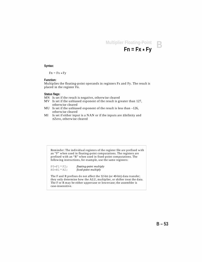
BCompute Operations
B – 53
Syntax:
Fn = Fx * Fy
Function:Multiplies the floating-point operands in registers Fx and Fy. The result isplaced in the register Fn.
Status flags:MN Is set if the result is negative, otherwise clearedMV Is set if the unbiased exponent of the result is greater than 127,
otherwise clearedMU Is set if the unbiased exponent of the result is less than –126,
otherwise clearedMI Is set if either input is a NAN or if the inputs are ±Infinity and
±Zero, otherwise cleared
Multiplier Floating-PointFn = Fx * Fy
Reminder: The individual registers of the register file are prefixed withan “F” when used in floating-point computations. The registers areprefixed with an “R” when used in fixed-point computations. Thefollowing instructions, for example, use the same registers:
F0=F1 * F2; floating-point multiplyR0=R1 * R2; fixed-point multiply
The F and R prefixes do not affect the 32-bit (or 40-bit) data transfer;they only determine how the ALU, multiplier, or shifter treat the data.The F or R may be either uppercase or lowercase; the assembler iscase-insensitive.
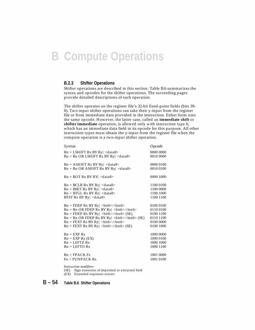
B Compute Operations
B – 54
B.2.3 Shifter OperationsShifter operations are described in this section. Table B.6 summarizes thesyntax and opcodes for the shifter operations. The succeeding pagesprovide detailed descriptions of each operation.
The shifter operates on the register file’s 32-bit fixed-point fields (bits 39-8). Two-input shifter operations can take their y-input from the registerfile or from immediate data provided in the instruction. Either form usesthe same opcode. However, the latter case, called an immediate shift orshifter immediate operation, is allowed only with instruction type 6,which has an immediate data field in its opcode for this purpose. All otherinstruction types must obtain the y-input from the register file when thecompute operation is a two-input shifter operation.
Syntax OpcodeRn = LSHIFT Rx BY Ry|<data8> 0000 0000Rn = Rn OR LSHIFT Rx BY Ry|<data8> 0010 0000
Rn = ASHIFT Rx BY Ry|<data8> 0000 0100Rn = Rn OR ASHIFT Rx BY Ry|<data8> 0010 0100
Rn = ROT Rx BY RY|<data8> 0000 1000
Rn = BCLR Rx BY Ry|<data8> 1100 0100Rn = BSET Rx BY Ry|<data8> 1100 0000Rn = BTGL Rx BY Ry|<data8> 1100 1000BTST Rx BY Ry|<data8> 1100 1100
Rn = FDEP Rx BY Ry|<bit6>:<len6> 0100 0100Rn = Rn OR FDEP Rx BY Ry|<bit6>:<len6> 0110 0100Rn = FDEP Rx BY Ry|<bit6>:<len6> (SE) 0100 1100Rn = Rn OR FDEP Rx BY Ry|<bit6>:<len6> (SE) 0110 1100Rn = FEXT Rx BY Ry|<bit6>:<len6> 0100 0000Rn = FEXT Rx BY Ry|<bit6>:<len6> (SE) 0100 1000
Rn = EXP Rx 1000 0000Rn = EXP Rx (EX) 1000 0100Rn = LEFTZ Rx 1000 1000Rn = LEFTO Rx 1000 1100
Rn = FPACK Fx 1001 0000Fn = FUNPACK Rx 1001 0100
Instruction modifiers:(SE) Sign extension of deposited or extracted field(EX) Extended exponent extract
Table B.6 Shifter Operations
BCompute Operations
B – 55
Syntax:
Rn = LSHIFT Rx BY RyRn = LSHIFT Rx BY <data8>
Function:Logically shifts the fixed-point operand in register Rx by the 32-bit valuein register Ry or by the 8-bit immediate value in the instruction. Theshifted result is placed in the fixed-point field of register Rn. The floating-point extension field of Rn is set to all 0s. The shift values are twos-complement numbers. Positive values select a left shift, negative valuesselect a right shift. The 8-bit immediate data can take values between –128and 127 inclusive, allowing for a shift of a 32-bit field from off-scale rightto off-scale left.
Status flags:SZ Is set if the shifted result is zero, otherwise clearedSV Is set if the input is shifted to the left by more than 0, otherwise
clearedSS Is cleared
ShifterRn = LSHIFT Rx BY Ry|<data8>

B Compute Operations
B – 56
Syntax:
Rn = Rn OR LSHIFT Rx BY RyRn = Rn OR LSHIFT Rx BY <data8>
Function:Logically shifts the fixed-point operand in register Rx by the 32-bit valuein register Ry or by the 8-bit immediate value in the instruction. Theshifted result is logically ORed with the fixed-point field of register Rnand then written back to register Rn. The floating-point extension field ofRn is set to all 0s. The shift values are twos-complement numbers. Positivevalues select a left shift, negative values select a right shift. The 8-bitimmediate data can take values between –128 and 127 inclusive, allowingfor a shift of a 32-bit field from off-scale right to off-scale left.
Status flags:SZ Is set if the shifted result is zero, otherwise clearedSV Is set if the input is shifted left by more than 0, otherwise clearedSS Is cleared
ShifterRn = Rn OR LSHIFT Rx BY Ry|<data8>
BCompute Operations
B – 57
Syntax:
Rn = ASHIFT Rx BY RyRn = ASHIFT Rx BY <data8>
Function:Arithmetically shifts the fixed-point operand in register Rx by the 32-bitvalue in register Ry or by the 8-bit immediate value in the instruction. Theshifted result is placed in the fixed-point field of register Rn. The floating-point extension field of Rn is set to all 0s. The shift values are twos-complement numbers. Positive values select a left shift, negative valuesselect a right shift. The 8-bit immediate data can take values between –128and 127 inclusive, allowing for a shift of a 32-bit field from off-scale rightto off-scale left.
Status flags:SZ Is set if the shifted result is zero , otherwise clearedSV Is set if the input is shifted left by more than 0, otherwise clearedSS Is cleared
ShifterRn = ASHIFT Rx BY Ry|<data8>
B Compute Operations
B – 58
Syntax:
Rn = Rn OR ASHIFT Rx BY RyRn = Rn OR ASHIFT Rx BY <data8>
Function:Arithmetically shifts the fixed-point operand in register Rx by the 32-bitvalue in register Ry or by the 8-bit immediate value in the instruction. Theshifted result is logically ORed with the fixed-point field of register Rnand then written back to register Rn. The floating-point extension field ofRn is set to all 0s. The shift values are twos-complement numbers. Positivevalues select a left shift, negative values select a right shift. The 8-bitimmediate data can take values between –128 and 127 inclusive, allowingfor a shift of a 32-bit field from off-scale right to off-scale left.
Status flags:SZ Is set if the shifted result is zero, otherwise clearedSV Is set if the input is shifted left by more than 0, otherwise clearedSS Is cleared
ShifterRn = Rn OR ASHIFT Rx BY Ry|<data8>

BCompute Operations
B – 59
Syntax:
Rn = ROT Rx BY RyRn = ROT Rx BY <data8>
Function:Rotates the fixed-point operand in register Rx by the 32-bit value inregister Ry or by the 8-bit immediate value in the instruction. The rotatedresult is placed in the fixed-point field of register Rn. The floating-pointextension field of Rn is set to all 0s. The shift values are twos-complementnumbers. Positive values select a rotate left; negative values select a rotateright. The 8-bit immediate data can take values between –128 and 127inclusive, allowing for a rotate of a 32-bit field from full right wrap aroundto full left wrap around.
Status flags:SZ Is set if the rotated result is zero, otherwise clearedSV Is clearedSS Is cleared
ShifterRn = ROT Rx BY Ry|<data8>

B Compute Operations
B – 60
Syntax:
Rn = BCLR Rx BY RyRn = BCLR Rx BY <data8>
Function:Clears a bit in the fixed-point operand in register Rx. The result is placedin the fixed-point field of register Rn. The floating-point extension field ofRn is set to all 0s. The position of the bit is the 32-bit value in register Ry orthe 8-bit immediate value in the instruction. The 8-bit immediate data cantake values between 31 and 0 inclusive, allowing for any bit within a 32-bitfield to be cleared. If the bit position value is greater than 31 or less than 0,no bits are cleared.
Status flags:SZ Is set if the output operand is 0, otherwise clearedSV Is set if the bit position is greater than 31, otherwise clearedSS Is cleared
Note: This compute operation affects a bit in a register file location. Thereis also a bit manipulation instruction that affects one or more bits in asystem register. This BIT CLR instruction should not be confused with theBCLR shifter operation. See Appendix E for more information on BITCLR.
ShifterRn = BCLR Rx BY Ry|<data8>

BCompute Operations
B – 61
Syntax:
Rn = BSET Rx BY RyRn = BSET Rx BY <data8>
Function:Sets a bit in the fixed-point operand in register Rx. The result is placed inthe fixed-point field of register Rn. The floating-point extension field of Rnis set to all 0s. The position of the bit is the 32-bit value in register Ry orthe 8-bit immediate value in the instruction. The 8-bit immediate data cantake values between 31 and 0 inclusive, allowing for any bit within a 32-bitfield to be set. If the bit position value is greater than 31 or less than 0, nobits are set.
Status flags:SZ Is set if the output operand is 0, otherwise clearedSV Is set if the bit position is greater than 31, otherwise clearedSS Is cleared
Note: This compute operation affects a bit in a register file location. Thereis also a bit manipulation instruction that affects one or more bits in asystem register. This BIT SET instruction should not be confused with theBSET shifter operation. See Appendix E for more information on BIT SET.
ShifterRn = BSET Rx BY Ry|<data8>
B Compute Operations
B – 62
Syntax:
Rn = BTGL Rx BY RyRn = BTGL Rx BY <data8>
Function:Toggles a bit in the fixed-point operand in register Rx. The result is placedin the fixed-point field of register Rn. The floating-point extension field ofRn is set to all 0s. The position of the bit is the 32-bit value in register Ry orthe 8-bit immediate value in the instruction. The 8-bit immediate data cantake values between 31 and 0 inclusive, allowing for any bit within a 32-bitfield to be toggled. If the bit position value is greater than 31 or less than 0,no bits are toggled.
Status flags:SZ Is set if the output operand is 0, otherwise clearedSV Is set if the bit position is greater than 31, otherwise clearedSS Is cleared
Note: This compute operation affects a bit in a register file location. Thereis also a bit manipulation instruction that affects one or more bits in asystem register. This BIT TGL instruction should not be confused with theBTGL shifter operation. See Appendix E for more information on BITTGL.
ShifterRn = BTGL Rx BY Ry|<data8>

BCompute Operations
B – 63
Syntax:
BTST Rx BY RyBTST Rx BY <data8>
Function:Tests a bit in the fixed-point operand in register Rx. The SZ flag is set if thebit is a 0 and cleared if the bit is a 1. The position of the bit is the 32-bitvalue in register Ry or the 8-bit immediate value in the instruction. The8-bit immediate data can take values between 31 and 0 inclusive, allowingfor any bit within a 32-bit field to be tested. If the bit position value isgreater than 31 or less than 0, no bits are tested.
Status flags:SZ Is cleared if the tested bit is a 1, is set if the tested bit is a 0 or if the
bit position is greater than 31SV Is set if the bit position is greater than 31, otherwise clearedSS Is cleared
Note: This compute operation tests a bit in a register file location. There isalso a bit manipulation instruction that tests one or more bits in a systemregister. This BIT TST instruction should not be confused with the BTSTshifter operation. See Appendix E for more information on BIT TST.
ShifterBTST Rx BY Ry|<data8>

B Compute Operations
B – 64
ShifterRn = FDEP Rx BY Ry|<bit6>:<len6>
Syntax:Rn = FDEP Rx BY RyRn = FDEP Rx BY <bit6>:<len6>
Function:Deposits a field from register Rx to register Rn. The input field is right-alignedwithin the fixed-point field of Rx. Its length is determined by the len6 field inregister Ry or by the immediate len6 field in the instruction. The field isdeposited in the fixed-point field of Rn, starting from a bit position determinedby the bit6 field in register Ry or by the immediate bit6 field in the instruction.Bits to the left and to the right of the deposited field are set to 0. The floating-pt.extension field of Rn (bits 7-0 of the 40-bit word) is set to all 0s. Bit6 and len6 cantake values between 0 and 63 inclusive, allowing for deposit of fields ranging inlength from 0 to 32 bits, and to bit positions ranging from 0 to off-scale left.
Example: If len6=14 and bit6=13, then the 14 bits of Rx are deposited in Rn bits34-21 (of the 40-bit word).
39 31 23 15 7 0|--------|--------|--abcdef|ghijklmn|--------| Rx \-------------/
14 bits
39 31 23 15 7 0|00000abc|defghijk|lmn00000|00000000|00000000| Rn \--------------/ |
bit position 13 (from reference point)Status flags:SZ Is set if the output operand is 0, otherwise clearedSV Is set if any bits are deposited to the left of the 32-bit fixed-point output
field (i.e., if len6 + bit6 > 32), otherwise clearedSS Is cleared
039
len6
719
bit6
13
Ry
039 7
Rx
len6 = number of bits to take from Rx, starting from LSB of 32-bit field
039 7
Rn
bit6 = starting bit position for deposit, referenced from LSB of 32-bit field
deposit field
bit6 reference point
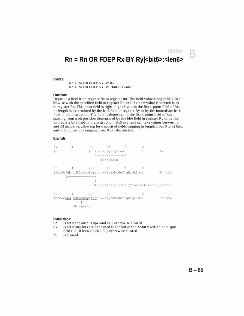
BCompute Operations
B – 65
ShifterRn = Rn OR FDEP Rx BY Ry|<bit6>:<len6>
Syntax:Rn = Rn OR FDEP Rx BY RyRn = Rn OR FDEP Rx BY <bit6>:<len6>
Function:Deposits a field from register Rx to register Rn. The field value is logically ORedbitwise with the specified field of register Rn and the new value is written backto register Rn. The input field is right-aligned within the fixed-point field of Rx.Its length is determined by the len6 field in register Ry or by the immediate len6field in the instruction. The field is deposited in the fixed-point field of Rn,starting from a bit position determined by the bit6 field in register Ry or by theimmediate bit6 field in the instruction. Bit6 and len6 can take values between 0and 63 inclusive, allowing for deposit of fields ranging in length from 0 to 32 bits,and to bit positions ranging from 0 to off-scale left.
Example:
39 31 23 15 7 0|--------|--------|--abcdef|ghijklmn|--------| Rx \--------------/
len6 bits
39 31 23 15 7 0|abcdefgh|ijklmnop|qrstuvwx|yzabcdef|ghijklmn| Rn old \--------------/ |
bit position bit6 (from reference point)
39 31 23 15 7 0|abcdeopq|rstuvwxy|zabtuvwx|yzabcdef|ghijklmn| Rn new
|OR result
Status flags:SZ Is set if the output operand is 0, otherwise clearedSV Is set if any bits are deposited to the left of the 32-bit fixed-point output
field (i.e., if len6 + bit6 > 32), otherwise clearedSS Is cleared

B Compute Operations
B – 66
Syntax:Rn = FDEP Rx BY Ry (SE)Rn = FDEP Rx BY <bit6>:<len6> (SE)
Function:Deposits and sign-extends a field from register Rx to register Rn. The input fieldis right-aligned within the fixed-point field of Rx. Its length is determined by thelen6 field in register Ry or by the immediate len6 field in the instruction. Thefield is deposited in the fixed-point field of Rn, starting from a bit positiondetermined by the bit6 field in register Ry or by the immediate bit6 field in theinstruction. The MSBs of Rn are sign-extended by the MSB of the deposited field,unless the MSB of the deposited field is off-scale left. Bits to the right of thedeposited field are set to 0. The floating-point extension field of Rn (bits 7-0 of the40-bit word) is set to all 0s. Bit6 and len6 can take values between 0 and 63inclusive, allowing for deposit of fields ranging in length from 0 to 32 bits into bitpositions ranging from 0 to off-scale left.
Example:39 31 23 15 7 0|--------|--------|--abcdef|ghijklmn|--------| Rx \---------------/
len6 bits
39 31 23 15 7 0|aaaaaabc|defghijk|lmn00000|00000000|00000000| Rn\----/\--------------/sign |extension bit position bit6 (from reference point)
Status flags:SZ Is set if the output operand is 0, otherwise clearedSV Is set if any bits are deposited to the left of the 32-bit fixed-point output
field (i.e., if len6 + bit6 > 32), otherwise clearedSS Is cleared
039
len6
719
bit6
13
Ry
039 7
Rx
len6 = number of bits to take from Rx, starting from LSB of 32-bit field
039 7
Rn
bit6 = starting bit position for deposit, referenced from LSB of 32-bit field
deposit field
bit6 reference point
sign bit extension
ShifterRn = FDEP Rx BY Ry|<bit6>:<len6> (SE)
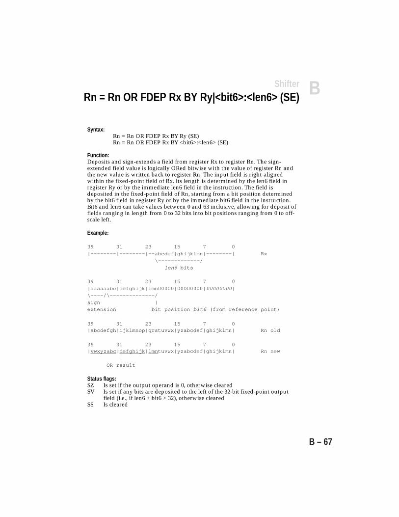
BCompute Operations
B – 67
Syntax:Rn = Rn OR FDEP Rx BY Ry (SE)Rn = Rn OR FDEP Rx BY <bit6>:<len6> (SE)
Function:Deposits and sign-extends a field from register Rx to register Rn. The sign-extended field value is logically ORed bitwise with the value of register Rn andthe new value is written back to register Rn. The input field is right-alignedwithin the fixed-point field of Rx. Its length is determined by the len6 field inregister Ry or by the immediate len6 field in the instruction. The field isdeposited in the fixed-point field of Rn, starting from a bit position determinedby the bit6 field in register Ry or by the immediate bit6 field in the instruction.Bit6 and len6 can take values between 0 and 63 inclusive, allowing for deposit offields ranging in length from 0 to 32 bits into bit positions ranging from 0 to off-scale left.
Example:
39 31 23 15 7 0|--------|--------|--abcdef|ghijklmn|--------| Rx \-------------/
len6 bits
39 31 23 15 7 0|aaaaaabc|defghijk|lmn00000|00000000|00000000|\----/\--------------/sign |extension bit position bit6 (from reference point)
39 31 23 15 7 0|abcdefgh|ijklmnop|qrstuvwx|yzabcdef|ghijklmn| Rn old
39 31 23 15 7 0|vwxyzabc|defghijk|lmntuvwx|yzabcdef|ghijklmn| Rn new | OR result
Status flags:SZ Is set if the output operand is 0, otherwise clearedSV Is set if any bits are deposited to the left of the 32-bit fixed-point output
field (i.e., if len6 + bit6 > 32), otherwise clearedSS Is cleared
ShifterRn = Rn OR FDEP Rx BY Ry|<bit6>:<len6> (SE)
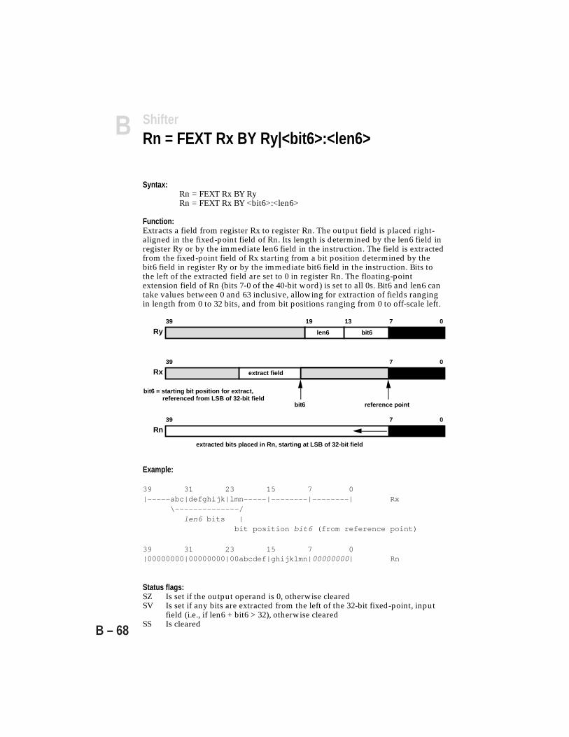
B Compute Operations
B – 68
ShifterRn = FEXT Rx BY Ry|<bit6>:<len6>
039
len6
719
bit6
13
Ry
039 7
Rn
extracted bits placed in Rn, starting at LSB of 32-bit field
039 7
Rx
bit6 = starting bit position for extract, referenced from LSB of 32-bit field
extract field
bit6 reference point
Syntax:Rn = FEXT Rx BY RyRn = FEXT Rx BY <bit6>:<len6>
Function:Extracts a field from register Rx to register Rn. The output field is placed right-aligned in the fixed-point field of Rn. Its length is determined by the len6 field inregister Ry or by the immediate len6 field in the instruction. The field is extractedfrom the fixed-point field of Rx starting from a bit position determined by thebit6 field in register Ry or by the immediate bit6 field in the instruction. Bits tothe left of the extracted field are set to 0 in register Rn. The floating-pointextension field of Rn (bits 7-0 of the 40-bit word) is set to all 0s. Bit6 and len6 cantake values between 0 and 63 inclusive, allowing for extraction of fields rangingin length from 0 to 32 bits, and from bit positions ranging from 0 to off-scale left.
Example:
39 31 23 15 7 0|-----abc|defghijk|lmn-----|--------|--------| Rx \--------------/
len6 bits | bit position bit6 (from reference point)
39 31 23 15 7 0|00000000|00000000|00abcdef|ghijklmn|00000000| Rn
Status flags:SZ Is set if the output operand is 0, otherwise clearedSV Is set if any bits are extracted from the left of the 32-bit fixed-point, input
field (i.e., if len6 + bit6 > 32), otherwise clearedSS Is cleared
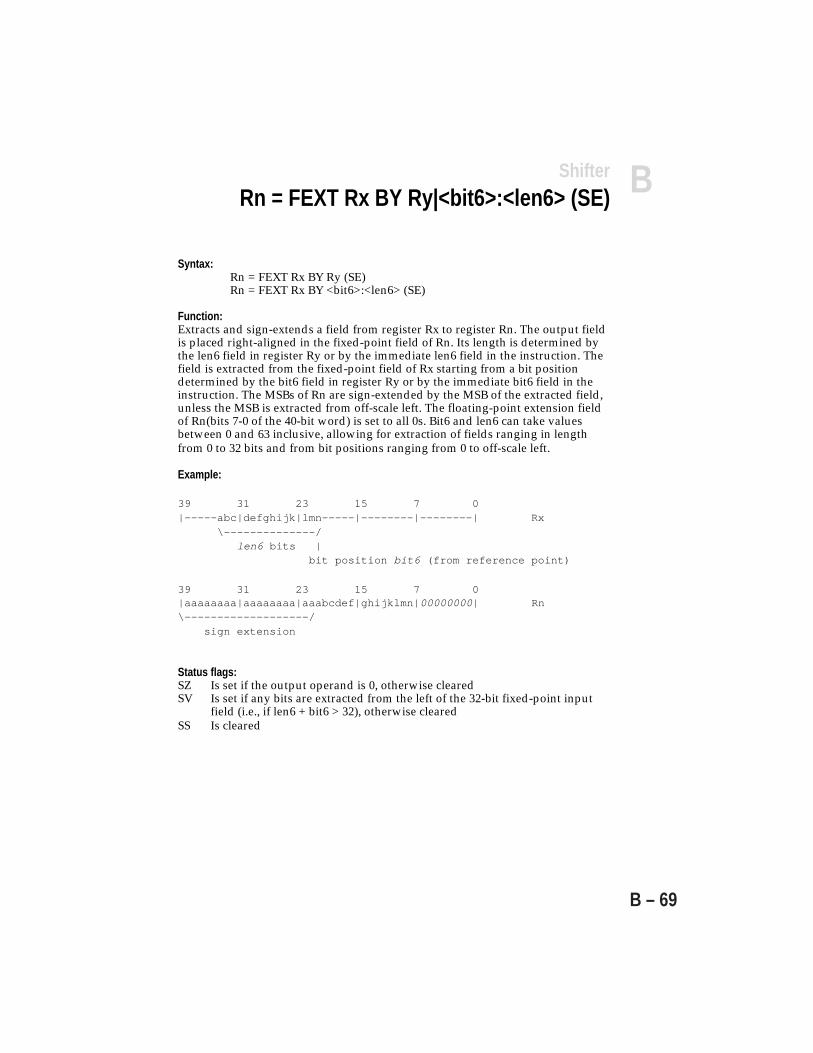
BCompute Operations
B – 69
ShifterRn = FEXT Rx BY Ry|<bit6>:<len6> (SE)
Syntax:Rn = FEXT Rx BY Ry (SE)Rn = FEXT Rx BY <bit6>:<len6> (SE)
Function:Extracts and sign-extends a field from register Rx to register Rn. The output fieldis placed right-aligned in the fixed-point field of Rn. Its length is determined bythe len6 field in register Ry or by the immediate len6 field in the instruction. Thefield is extracted from the fixed-point field of Rx starting from a bit positiondetermined by the bit6 field in register Ry or by the immediate bit6 field in theinstruction. The MSBs of Rn are sign-extended by the MSB of the extracted field,unless the MSB is extracted from off-scale left. The floating-point extension fieldof Rn(bits 7-0 of the 40-bit word) is set to all 0s. Bit6 and len6 can take valuesbetween 0 and 63 inclusive, allowing for extraction of fields ranging in lengthfrom 0 to 32 bits and from bit positions ranging from 0 to off-scale left.
Example:
39 31 23 15 7 0|-----abc|defghijk|lmn-----|--------|--------| Rx \--------------/
len6 bits | bit position bit6 (from reference point)
39 31 23 15 7 0|aaaaaaaa|aaaaaaaa|aaabcdef|ghijklmn|00000000| Rn\-------------------/ sign extension
Status flags:SZ Is set if the output operand is 0, otherwise clearedSV Is set if any bits are extracted from the left of the 32-bit fixed-point input
field (i.e., if len6 + bit6 > 32), otherwise clearedSS Is cleared

B Compute Operations
B – 70
Syntax:
Rn = EXP Rx
Function:Extracts the exponent of the fixed-point operand in Rx. The exponent isplaced in the shf8 field in register Rn. The exponent is calculated as thetwos complement of:
# leading sign bits in Rx – 1
Status flags:SZ Is set if the extracted exponent is 0, otherwise clearedSV Is clearedSS Is set if the fixed-point operand in Rx is negative (bit 31 is a 1),
otherwise cleared
ShifterRn = EXP Rx
BCompute Operations
B – 71
Syntax:
Rn = EXP Rx (EX)
Function:Extracts the exponent of the fixed-point operand in Rx, assuming that theoperand is the result of an ALU operation. The exponent is placed in theshf8 field in register Rn. If the AV status bit is set, a value of +1 is placedin the shf8 field to indicate an extra bit (the ALU overflow bit). If the AVstatus bit is not set, the exponent is calculated as the twos complement of:
# leading sign bits in Rx – 1
Status flags:SZ Is set if the extracted exponent is 0, otherwise clearedSV Is clearedSS Is set if the exclusive OR of the AV status bit and the sign bit (bit 31)
of the fixed-point operand in Rx is equal to 1, otherwise cleared
ShifterRn = EXP Rx (EX)
B Compute Operations
B – 72
ShifterRn = LEFTZ Rx
Syntax:
Rn = LEFTZ Rx
Function:Extracts the number of leading 0s from the fixed-point operand in Rx. Theextracted number is placed in the bit6 field in Rn.
Status flags:SZ Is set if the MSB of Rx is 1, otherwise clearedSV Is set if the result is 32, otherwise clearedSS Is cleared

BCompute Operations
B – 73
Syntax:
Rn = LEFTO Rx
Function:Extracts the number of leading 1s from the fixed-point operand in Rx. Theextracted number is placed in the bit6 field in Rn.
Status flags:SZ Is set if the MSB of Rx is 0, otherwise clearedSV Is set if the result is 32, otherwise clearedSS Is cleared
ShifterRn = LEFTO Rx
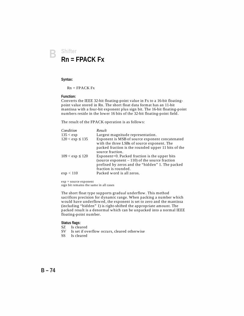
B Compute Operations
B – 74
ShifterRn = FPACK Fx
Syntax:
Rn = FPACK Fx
Function:Converts the IEEE 32-bit floating-point value in Fx to a 16-bit floating-point value stored in Rn. The short float data format has an 11-bitmantissa with a four-bit exponent plus sign bit. The 16-bit floating-pointnumbers reside in the lower 16 bits of the 32-bit floating-point field.
The result of the FPACK operation is as follows:
Condition Result135 < exp Largest magnitude representation.120 < exp ≤ 135 Exponent is MSB of source exponent concatenated
with the three LSBs of source exponent. Thepacked fraction is the rounded upper 11 bits of thesource fraction.
109 < exp ≤ 120 Exponent=0. Packed fraction is the upper bits(source exponent – 110) of the source fractionprefixed by zeros and the “hidden” 1. The packedfraction is rounded.
exp < 110 Packed word is all zeros.
exp = source exponentsign bit remains the same in all cases
The short float type supports gradual underflow. This methodsacrifices precision for dynamic range. When packing a number whichwould have underflowed, the exponent is set to zero and the mantissa(including “hidden” 1) is right-shifted the appropriate amount. Thepacked result is a denormal which can be unpacked into a normal IEEEfloating-point number.
Status flags:SZ Is clearedSV Is set if overflow occurs, cleared otherwiseSS Is cleared

BCompute Operations
B – 75
Syntax:
Fn = FUNPACK Rx
Function:Converts the 16-bit floating-point value in Rx to an IEEE 32-bit floating-point value stored in Fx.
The result of the FUNPACK operation is as follows:
Condition Result0 < exp ≤ 15 Exponent is the 3 LSBs of the source exponent
prefixed by the MSB of the source exponent andfour copies of the complement of the MSB. Theunpacked fraction is the source fraction with 12zeros appended.
exp = 0 Exponent is (120 – N) where N is the number ofleading zeros in the source fraction. The unpackedfraction is the remainder of the source fractionwith zeros appended to pad it and the “hidden” 1stripped away.
exp = source exponentsign bit remains the same in all cases
The short float type supports gradual underflow. This methodsacrifices precision for dynamic range. When packing a number whichwould have underflowed, the exponent is set to zero and the mantissa(including “hidden” 1) is right-shifted the appropriate amount. Thepacked result is a denormal which can be unpacked into a normal IEEEfloating-point number.
Status flags:SZ Is clearedSV Is clearedSS Is cleared
ShifterFx = FUNPACK Rn

B Compute Operations
B – 76
B.3 MULTIFUNCTION COMPUTATIONSMultifunction computations are of three types, each of which has adifferent format for the 23-bit compute field:
• Dual add/subtract• Parallel multiplier/ALU• Parallel multiplier and add/subtract
See “Multifunction Computations” in the Computation Units chapter for asummary of the multifunction operations.
Each of the four input operands for multifunction computations areconstrained to a different set of four register file locations, as shown belowin Figure B.1. For example, the X-input to the ALU can only be R8, R9, R10or R11. In all other compute operations, the input operands may be anyregister file locations.
R0 - F0R1 - F1R2 - F2
R3 - F3
R4 - F4R5 - F5
R6 - F6R7 - F7
R8 - F8R9 - F9
R10 - F10R11 - F11
R12 - F12R13 - F13
R14 - F14R15 - F15
Multiplier
ALU
Any Register
Any Register
Register File
Figure B.1 Allowed Input Registers For Multifunction Computations
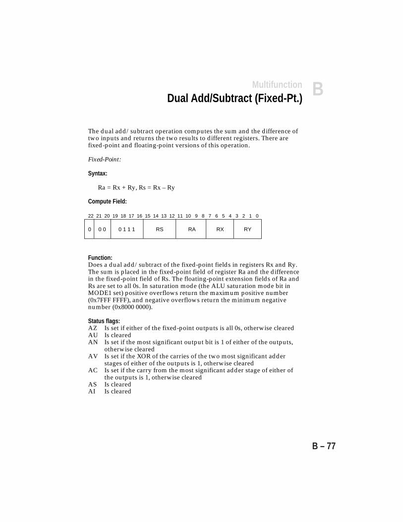
BCompute Operations
B – 77
MultifunctionDual Add/Subtract (Fixed-Pt.)
The dual add/subtract operation computes the sum and the difference oftwo inputs and returns the two results to different registers. There arefixed-point and floating-point versions of this operation.
Fixed-Point:
Syntax:
Ra = Rx + Ry, Rs = Rx – Ry
Compute Field:
22 21 20 19 18 17 16 15 14 13 12 11 10 9 8 7 6 5 4 3 2 1 0
0 0 0 0 1 1 1 RS RA RX RY
Function:Does a dual add/subtract of the fixed-point fields in registers Rx and Ry.The sum is placed in the fixed-point field of register Ra and the differencein the fixed-point field of Rs. The floating-point extension fields of Ra andRs are set to all 0s. In saturation mode (the ALU saturation mode bit inMODE1 set) positive overflows return the maximum positive number(0x7FFF FFFF), and negative overflows return the minimum negativenumber (0x8000 0000).
Status flags:AZ Is set if either of the fixed-point outputs is all 0s, otherwise clearedAU Is clearedAN Is set if the most significant output bit is 1 of either of the outputs,
otherwise clearedAV Is set if the XOR of the carries of the two most significant adder
stages of either of the outputs is 1, otherwise clearedAC Is set if the carry from the most significant adder stage of either of
the outputs is 1, otherwise clearedAS Is clearedAI Is cleared
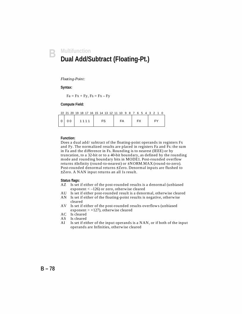
B Compute Operations
B – 78
Floating-Point:
Syntax:
Fa = Fx + Fy, Fs = Fx – Fy
Compute Field:
22 21 20 19 18 17 16 15 14 13 12 11 10 9 8 7 6 5 4 3 2 1 0
0 0 0 1 1 1 1 FS FA FX FY
Function:Does a dual add/subtract of the floating-point operands in registers Fxand Fy. The normalized results are placed in registers Fa and Fs: the sumin Fa and the difference in Fs. Rounding is to nearest (IEEE) or bytruncation, to a 32-bit or to a 40-bit boundary, as defined by the roundingmode and rounding boundary bits in MODE1. Post-rounded overflowreturns ±Infinity (round-to-nearest) or ±NORM.MAX (round-to-zero).Post-rounded denormal returns ±Zero. Denormal inputs are flushed to±Zero. A NAN input returns an all 1s result.
Status flags:AZ Is set if either of the post-rounded results is a denormal (unbiased
exponent < –126) or zero, otherwise clearedAU Is set if either post-rounded result is a denormal, otherwise clearedAN Is set if either of the floating-point results is negative, otherwise
clearedAV Is set if either of the post-rounded results overflows (unbiased
exponent > +127), otherwise clearedAC Is clearedAS Is clearedAI Is set if either of the input operands is a NAN, or if both of the input
operands are Infinities, otherwise cleared
MultifunctionDual Add/Subtract (Floating-Pt.)
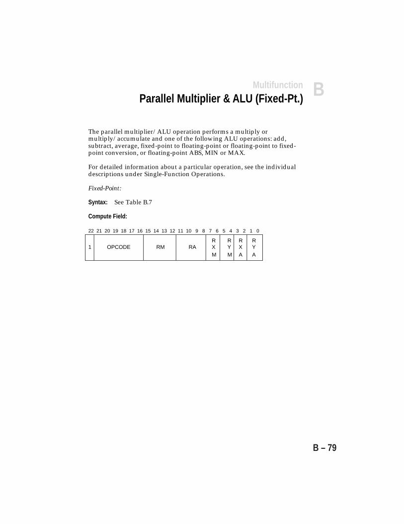
BCompute Operations
B – 79
The parallel multiplier/ALU operation performs a multiply ormultiply/accumulate and one of the following ALU operations: add,subtract, average, fixed-point to floating-point or floating-point to fixed-point conversion, or floating-point ABS, MIN or MAX.
For detailed information about a particular operation, see the individualdescriptions under Single-Function Operations.
Fixed-Point:
Syntax: See Table B.7
Compute Field:
22 21 20 19 18 17 16 15 14 13 12 11 10 9 8 7 6 5 4 3 2 1 0
R R R R1 OPCODE RM RA X Y X Y
M M A A
MultifunctionParallel Multiplier & ALU (Fixed-Pt.)
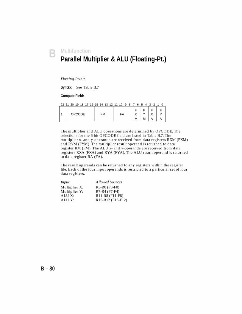
B Compute Operations
B – 80
Floating-Point:
Syntax: See Table B.7
Compute Field:
22 21 20 19 18 17 16 15 14 13 12 11 10 9 8 7 6 5 4 3 2 1 0
F F F F1 OPCODE FM FA X Y X Y
M M A A
The multiplier and ALU operations are determined by OPCODE. Theselections for the 6-bit OPCODE field are listed in Table B.7. Themultiplier x- and y-operands are received from data registers RXM (FXM)and RYM (FYM). The multiplier result operand is returned to dataregister RM (FM). The ALU x- and y-operands are received from dataregisters RXA (FXA) and RYA (FYA). The ALU result operand is returnedto data register RA (FA).
The result operands can be returned to any registers within the registerfile. Each of the four input operands is restricted to a particular set of fourdata registers.
Input Allowed SourcesMultiplier X: R3-R0 (F3-F0)Multiplier Y: R7-R4 (F7-F4)ALU X: R11-R8 (F11-F8)ALU Y: R15-R12 (F15-F12)
MultifunctionParallel Multiplier & ALU (Floating-Pt.)

BCompute Operations
B – 81
Syntax OpcodeRm=R3-0 * R7-4 (SSFR), Ra=R11-8 + R15-12 000100Rm=R3-0 * R7-4 (SSFR), Ra=R11-8 – R15-12 000101Rm=R3-0 * R7-4 (SSFR), Ra=(R11-8 + R15-12)/2 000110
MRF=MRF + R3-0 * R7-4 (SSF), Ra=R11-8 + R15-12 001000MRF=MRF + R3-0 * R7-4 (SSF), Ra=R11-8 – R15-12 001001MRF=MRF + R3-0 * R7-4 (SSF), Ra=(R11-8 + R15-12)/2 001010
Rm=MRF + R3-0 * R7-4 (SSFR), Ra=R11-8 + R15-12 001100Rm=MRF + R3-0 * R7-4 (SSFR), Ra=R11-8 – R15-12 001101Rm=MRF + R3-0 * R7-4 (SSFR), Ra=(R11-8 + R15-12)/2 001110
MRF=MRF – R3-0 * R7-4 (SSF), Ra=R11-8 + R15-12 010000MRF=MRF – R3-0 * R7-4 (SSF), Ra=R11-8 – R15-12 010001MRF=MRF – R3-0 * R7-4 (SSF), Ra=(R11-8 + R15-12)/2 010010
Rm=MRF – R3-0 * R7-4 (SSFR), Ra=R11-8 + R15-12 010100Rm=MRF – R3-0 * R7-4 (SSFR), Ra=R11-8 – R15-12 010101Rm=MRF – R3-0 * R7-4 (SSFR), Ra=(R11-8 + R15-12)/2 010110
Fm=F3-0 * F7-4, Fa=F11-8 + F15-12 011000Fm=F3-0 * F7-4, Fa=F11-8 – F15-12 011001Fm=F3-0 * F7-4, Fa=FLOAT R11-8 by R15-12 011010Fm=F3-0 * F7-4, Fa=FIX F11-8 by R15-12 011011Fm=F3-0 * F7-4, Fa=(F11-8 + F15-12)/2 011100Fm=F3-0 * F7-4, Fa=ABS F11-8 011101Fm=F3-0 * F7-4, Fa=MAX (F11-8, F15-12) 011110Fm=F3-0 * F7-4, Fa=MIN (F11-8, F15-12) 011111
Table B.7 Parallel Multiplier/ALU Computations

B Compute Operations
B – 82
The parallel multiplier and dual add/subtract operation performs amultiply or multiply/accumulate and computes the sum and thedifference of the ALU inputs. For detailed information on the multiplieroperations, see the individual descriptions under Single-FunctionOperations. For information on the dual add/subtract operation, see theDual Add/Subtract section.
Fixed-Point:
Syntax:
Rm=R3-0 * R7-4 (SSFR), Ra=R11-8 + R15-12, Rs=R11-8 – R15-12
Compute Field:
22 21 20 19 18 17 16 15 14 13 12 11 10 9 8 7 6 5 4 3 2 1 0
R R R R1 1 0 RS RM RA X Y X Y
M M A A
Floating-Point:
Syntax:
Fm=F3-0 * F7-4, Fa=F11-8 + F15-12, Fs=F11-8 – F15-12
Compute Field:
22 21 20 19 18 17 16 15 14 13 12 11 10 9 8 7 6 5 4 3 2 1 0
F F F F1 1 1 FS FM FA X Y X Y
M M A A
The multiplier x- and y-operands are received from data registers RXM(FXM) and RYM (FYM). The multiplier result operand is returned to dataregister RM (FM). The ALU x- and y-operands are received from dataregisters RXA (FXA) and RYA (FYA). The ALU result operands arereturned to data register RA (FA) and RS (FS).
MultifunctionParallel Multiplier & Dual Add/Subtract
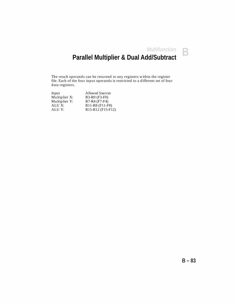
BCompute Operations
B – 83
The result operands can be returned to any registers within the registerfile. Each of the four input operands is restricted to a different set of fourdata registers.
Input Allowed SourcesMultiplier X: R3-R0 (F3-F0)Multiplier Y: R7-R4 (F7-F4)ALU X: R11-R8 (F11-F8)ALU Y: R15-R12 (F15-F12)
MultifunctionParallel Multiplier & Dual Add/Subtract

B Compute Operations
B – 84
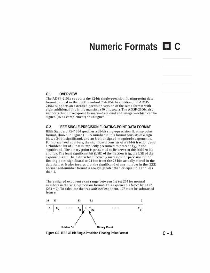
CNumeric Formats
C.1 OVERVIEWThe ADSP-2106x supports the 32-bit single-precision floating-point dataformat defined in the IEEE Standard 754/854. In addition, the ADSP-2106x supports an extended-precision version of the same format witheight additional bits in the mantissa (40 bits total). The ADSP-2106x alsosupports 32-bit fixed-point formats—fractional and integer—which can besigned (twos-complement) or unsigned.
C.2 IEEE SINGLE-PRECISION FLOATING-POINT DATA FORMATIEEE Standard 754/854 specifies a 32-bit single-precision floating-pointformat, shown in Figure C.1. A number in this format consists of a signbit s, a 24-bit significand, and an 8-bit unsigned-magnitude exponent e.For normalized numbers, the significand consists of a 23-bit fraction f anda “hidden” bit of 1 that is implicitly presumed to precede f22 in thesignificand. The binary point is presumed to lie between this hidden bitand f22. The least significant bit (LSB) of the fraction is f0; the LSB of theexponent is e0. The hidden bit effectively increases the precision of thefloating-point significand to 24 bits from the 23 bits actually stored in thedata format. It also insures that the significand of any number in the IEEEnormalized-number format is always greater than or equal to 1 and lessthan 2.
The unsigned exponent e can range between 1 ≤ e ≤ 254 for normalnumbers in the single-precision format. This exponent is biased by +127(254 ÷ 2). To calculate the true unbiased exponent, 127 must be subtractedfrom e.
Figure C.1 IEEE 32-Bit Single-Precision Floating-Point Format
s e e 1 . f f
31 30 23 22 0
22 07 0• • • • • •
Hidden Bit Binary Point
C – 1
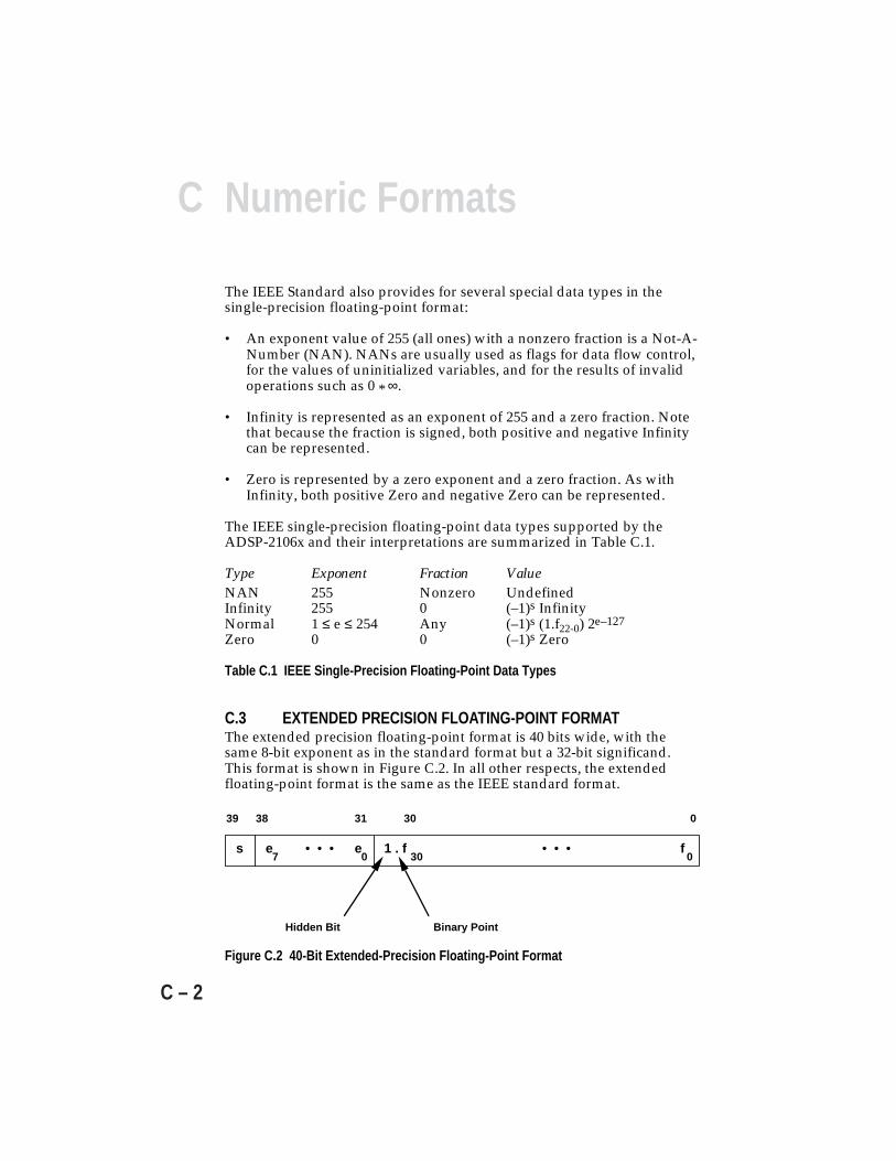
C Numeric Formats
C – 2
The IEEE Standard also provides for several special data types in thesingle-precision floating-point format:
• An exponent value of 255 (all ones) with a nonzero fraction is a Not-A-Number (NAN). NANs are usually used as flags for data flow control,for the values of uninitialized variables, and for the results of invalidoperations such as 0 * ∞.
• Infinity is represented as an exponent of 255 and a zero fraction. Notethat because the fraction is signed, both positive and negative Infinitycan be represented.
• Zero is represented by a zero exponent and a zero fraction. As withInfinity, both positive Zero and negative Zero can be represented.
The IEEE single-precision floating-point data types supported by theADSP-2106x and their interpretations are summarized in Table C.1.
Type Exponent Fraction ValueNAN 255 Nonzero UndefinedInfinity 255 0 (–1)s InfinityNormal 1 ≤ e ≤ 254 Any (–1)s (1.f22-0) 2e–127
Zero 0 0 (–1)s Zero
Table C.1 IEEE Single-Precision Floating-Point Data Types
C.3 EXTENDED PRECISION FLOATING-POINT FORMATThe extended precision floating-point format is 40 bits wide, with thesame 8-bit exponent as in the standard format but a 32-bit significand.This format is shown in Figure C.2. In all other respects, the extendedfloating-point format is the same as the IEEE standard format.
s e e 1 . f f
39 38 31 30 0
30 07 0• • • • • •
Hidden Bit Binary Point
Figure C.2 40-Bit Extended-Precision Floating-Point Format
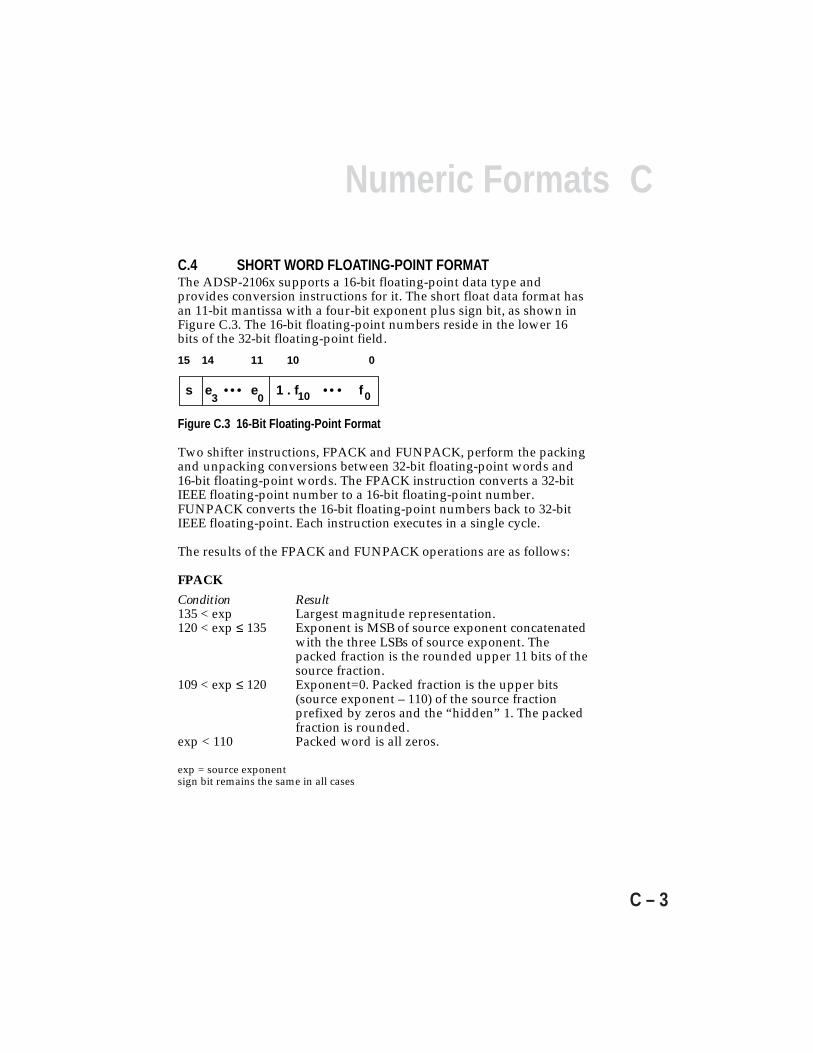
CNumeric Formats
C – 3
C.4 SHORT WORD FLOATING-POINT FORMATThe ADSP-2106x supports a 16-bit floating-point data type andprovides conversion instructions for it. The short float data format hasan 11-bit mantissa with a four-bit exponent plus sign bit, as shown inFigure C.3. The 16-bit floating-point numbers reside in the lower 16bits of the 32-bit floating-point field.
Figure C.3 16-Bit Floating-Point Format
Two shifter instructions, FPACK and FUNPACK, perform the packingand unpacking conversions between 32-bit floating-point words and16-bit floating-point words. The FPACK instruction converts a 32-bitIEEE floating-point number to a 16-bit floating-point number.FUNPACK converts the 16-bit floating-point numbers back to 32-bitIEEE floating-point. Each instruction executes in a single cycle.
The results of the FPACK and FUNPACK operations are as follows:
FPACK
Condition Result135 < exp Largest magnitude representation.120 < exp ≤ 135 Exponent is MSB of source exponent concatenated
with the three LSBs of source exponent. Thepacked fraction is the rounded upper 11 bits of thesource fraction.
109 < exp ≤ 120 Exponent=0. Packed fraction is the upper bits(source exponent – 110) of the source fractionprefixed by zeros and the “hidden” 1. The packedfraction is rounded.
exp < 110 Packed word is all zeros.
exp = source exponentsign bit remains the same in all cases
s e e 1 . f f
15 14 11 10 0
10 03 0• • • • • •

C Numeric Formats
C – 4
FUNPACK
Condition Result0 < exp ≤ 15 Exponent is the 3 LSBs of the source exponent
prefixed by the MSB of the source exponent andfour copies of the complement of the MSB. Theunpacked fraction is the source fraction with 12zeros appended.
exp = 0 Exponent is (120 – N) where N is the number ofleading zeros in the source fraction. The unpackedfraction is the remainder of the source fractionwith zeros appended to pad it and the “hidden” 1stripped away.
exp = source exponentsign bit remains the same in all cases
The short float type supports gradual underflow. This methodsacrifices precision for dynamic range. When packing a number whichwould have underflowed, the exponent is set to zero and the mantissa(including “hidden” 1) is right-shifted the appropriate amount. Thepacked result is a denormal which can be unpacked into a normal IEEEfloating-point number.
During the FPACK operation, an overflow will set the SV conditionand non-overflow will clear it. During the FUNPACK operation, theSV condition will be cleared. The SZ and SS conditions are cleared byboth instructions.
CNumeric Formats
C – 5
C.5 FIXED-POINT FORMATSThe ADSP-2106x supports two 32-bit fixed-point formats: fractional andinteger. In both formats, numbers can be signed (twos-complement) orunsigned. The four possible combinations are shown in Figure C.4. In thefractional format, there is an implied binary point to the left of the mostsignificant magnitude bit. In integer format, the binary point isunderstood to be to the right of the LSB. Note that the sign bit isnegatively weighted in a twos-complement format.
ALU outputs always have the same width and data format as the inputs.The multiplier, however, produces a 64-bit product from two 32-bitinputs. If both operands are unsigned integers, the result is a 64-bitunsigned integer. If both operands are unsigned fractions, the result is a64-bit unsigned fraction. These formats are shown in Figure C.5.
If one operand is signed and the other unsigned, the result is signed. Ifboth inputs are signed, the result is signed and automatically shifted leftone bit. The LSB becomes zero and bit 62 moves into the sign bit position.Normally bit 63 and bit 62 are identical when both operands are signed.(The only exception is full-scale negative multiplied by itself.) Thus, theleft shift normally removes a redundant sign bit, increasing the precisionof the most significant product. Also, if the data format is fractional, asingle-bit left shift renormalizes the MSP to a fractional format. The signedformats with and without left shifting are shown in Figure C.6.
The multiplier has an 80-bit accumulator to allow the accumulation of 64-bit products. The multiplier and accumulator are described in detail in theComputation Units chapter.

C Numeric Formats
C – 6
31 30 29
• • •
2 1 0
–2 2 2 2 2 231 30 29 2 1 0
SignBit
Weight
Bit
31 30 29
• • •
2 1 0
–2 2 2 2 2 20 –1 –2 –29 –30 –31
SignBit
Weight
BitSigned Fractional
Signed Integer
31 30 29
• • •
2 1 0
2 2 2 2 2 231 30 29 2 1 0
Weight
Bit
31 30 29
• • •
2 1 0
2 2 2 2 2 2–1 –2 –3 –30 –31 –32
Weight
Bit
Unsigned Integer
Unsigned Fractional
•
•
•
•
Binary point
Binary point
Binary point
Binary point
Figure C.4 32-Bit Fixed-Point Formats

CNumeric Formats
C – 7
63 62 61
• • •
2 1 0
2 2 2 2 2 263 62 61 2 1 0
Weight
Bit
63 62 61
• • •
2 1 0
2 2 2 2 2 2–1 –2 –3 –62 –63 –64
Weight
Bit
Unsigned Integer
Unsigned Fractional
Figure C.5 64-Bit Unsigned Fixed-Point Product
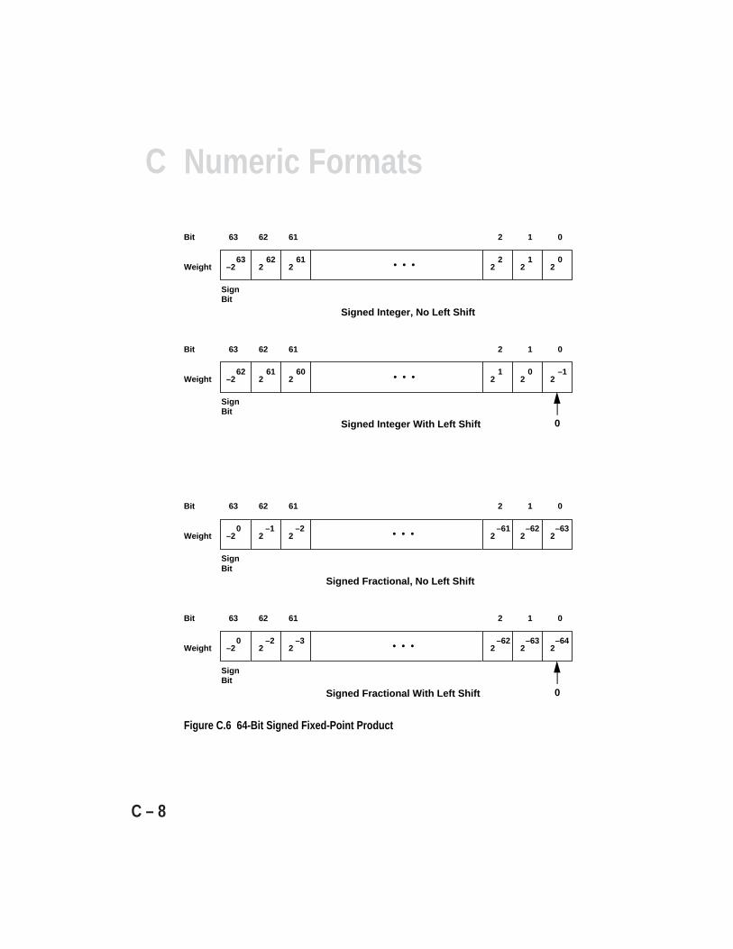
C Numeric Formats
C – 8
63 62 61
• • •
2 1 0
–2 2 2 2 2 263 62 61 2 1 0
SignBit
Weight
Bit
63 62 61
• • •
2 1 0
–2 2 2 2 2 20 –1 –2 –61 –62 –63
SignBit
Weight
Bit
Signed Integer, No Left Shift
Signed Fractional, No Left Shift
63 62 61
• • •
2 1 0
–2 2 2 2 2 262 61 60 1 0 –1
SignBit
Weight
Bit
Signed Integer With Left Shift
63 62 61
• • •
2 1 0
–2 2 2 2 2 20 –2 –3 –62 –63 –64
SignBit
Weight
Bit
Signed Fractional With Left Shift
0
0
Figure C.6 64-Bit Signed Fixed-Point Product
D
D – 1
JTAG Test Access Port
D.1 OVERVIEWA boundary scan allows a system designer to test interconnections on aprinted circuit board with minimal test-specific hardware. The scan ismade possible by the ability to control and monitor each input and outputpin on each chip through a set of serially scannable latches. Each inputand output is connected to a latch, and the latches are connected as a longshift register so that data can be read from or written to them through aserial test access port (TAP). The ADSP-2106x contains a test access portcompatible with the industry-standard IEEE 1149.1 (JTAG) specification.
Only the IEEE 1149.1 features specific to the ADSP-2106x are describedhere. For more information, see the IEEE 1149.1 specification and thereferences listed at the end of this appendix.
The boundary scan allows a variety of functions to be performed on eachinput and output signal of the ADSP-2106x. Each input has a latch thatmonitors the value of the incoming signal and can also drive data into thechip in place of the incoming value. Similarly, each output has a latch thatmonitors the outgoing signal and can also drive the output in place of theoutgoing value. For bidirectional pins, the combination of input andoutput functions is available.
Every latch associated with a pin is part of a single serial shift registerpath. Each latch is a master/slave type latch with the controlling clockprovided externally. This clock (TCK) is asynchronous to the ADSP-2106xsystem clock (CLKIN).
D JTAG Test Access Port
D – 2
D.2 TEST ACCESS PORTThe test access port (TAP) of the ADSP-2106x controls the operation ofthe boundary scan. The TAP consists of five pins that control a statemachine, including the boundary scan. The state machine and pinsconform to the IEEE 1149.1 specification.
TCK (input) Test Clock. Used to clock serial data into scan latches andcontrol sequencing of the test state machine. TCK can beasynchronous with CLKIN.
TMS (input) Test Mode Select. Primary control signal for the statemachine. Synchronous with TCK. A sequence of values onTMS adjusts the current state of the TAP.
TDI (input) Test Data Input. Serial input data to the scan latches.Synchronous with TCK.
TDO (output) Test Data Output. Serial output data from the scan latches.Synchronous with TCK.
TRST (input) Test Reset. Resets the test state machine. Can beasynchronous with TCK.
A BSDL file for the ADSP-2106x is available on Analog Devices’ BBSand Internet ftp site. The BBS can be reached at:
(617) 461-4258 8 data bits, no parity, 1 stop bit,300/1200/2400/9600/14400 baud
To connect to the ftp site, login as anonymous using your emailaddress for your password and type (from the Unix prompt):
ftp ftp.analog.com (or ftp 137.71.23.11)
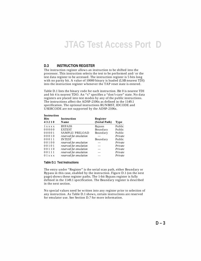
DJTAG Test Access Port
D – 3
D.3 INSTRUCTION REGISTERThe instruction register allows an instruction to be shifted into theprocessor. This instruction selects the test to be performed and/or thetest data register to be accessed. The instruction register is 5 bits longwith no parity bit. A value of 10000 binary is loaded (LSB nearest TDI)into the instruction register whenever the TAP reset state is entered.
Table D.1 lists the binary code for each instruction. Bit 0 is nearest TDIand bit 4 is nearest TDO. An “x” specifies a “don’t-care” state. No dataregisters are placed into test modes by any of the public instructions.The instructions affect the ADSP-2106x as defined in the 1149.1specification. The optional instructions RUNBIST, IDCODE andUSERCODE are not supported by the ADSP-2106x.
InstructionBits Instruction Register4 3 2 1 0 Name (Serial Path) Type1 x x x x BYPASS Bypass Public0 0 0 0 0 EXTEST Boundary Public0 0 0 0 1 SAMPLE/PRELOAD Boundary Public0 0 0 1 0 reserved for emulation — Private0 0 0 1 1 INTEST Boundary Public0 0 1 0 0 reserved for emulation — Private0 0 1 0 1 reserved for emulation — Private0 0 1 1 0 reserved for emulation — Private0 0 1 1 1 reserved for emulation — Private0 1 x x x reserved for emulation — Private
Table D.1 Test Instructions
The entry under “Register” is the serial scan path, either Boundary orBypass in this case, enabled by the instruction. Figure D.1 (on the nextpage) shows these register paths. The 1-bit Bypass register is fullydefined in the 1149.1 specification. The Boundary register is describedin the next section.
No special values need be written into any register prior to selection ofany instruction. As Table D.1 shows, certain instructions are reservedfor emulator use. See Section D.7 for more information.
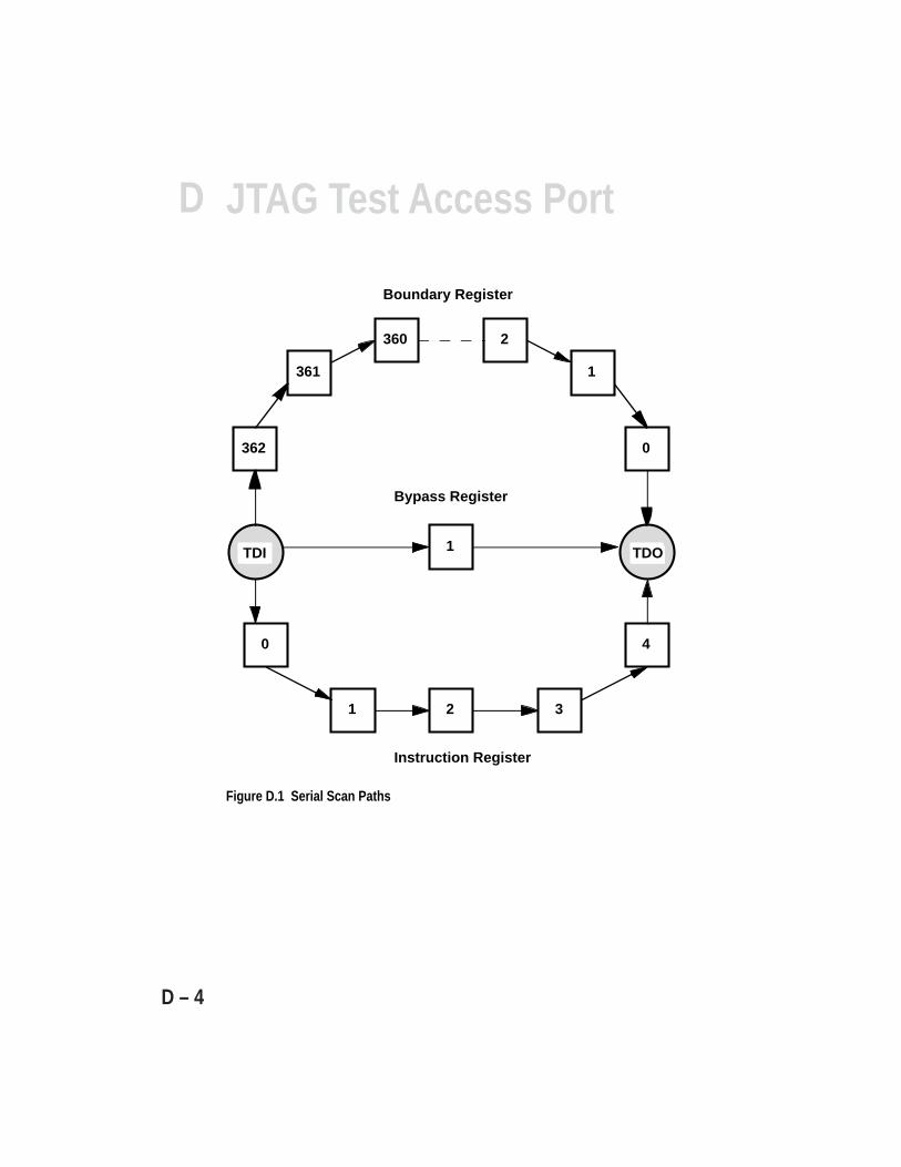
D JTAG Test Access Port
D – 4
TDI
0
1
2
362
361
360
Boundary Register
1
Bypass Register
31
0 4
Instruction Register
2
TDO
Figure D.1 Serial Scan Paths
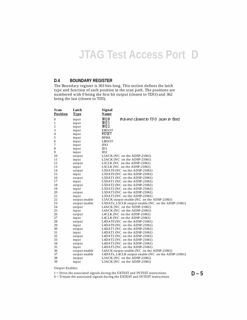
DJTAG Test Access Port
D – 5
D.4 BOUNDARY REGISTERThe Boundary register is 363 bits long. This section defines the latchtype and function of each position in the scan path. The positions arenumbered with 0 being the first bit output (closest to TDO) and 362being the last (closest to TDI).
Scan Latch SignalPosition Type Name0 input IRQ0 this end closest to TDO (scan in first)1 input IRQ12 input IRQ23 input EBOOT4 input RESET5 input RPBA6 input LBOOT7 input IDO8 input ID19 input ID210 output L5ACK (NC on the ADSP-21061)11 input L5ACK (NC on the ADSP-21061)12 output L5CLK (NC on the ADSP-21061)13 input L5CLK (NC on the ADSP-21061)14 output L5DAT0 (NC on the ADSP-21061)15 input L5DAT0 (NC on the ADSP-21061)16 output L5DAT1 (NC on the ADSP-21061)17 input L5DAT1 (NC on the ADSP-21061)18 output L5DAT2 (NC on the ADSP-21061)19 input L5DAT2 (NC on the ADSP-21061)20 output L5DAT3 (NC on the ADSP-21061)21 input L5DAT3 (NC on the ADSP-21061)22 output enable L5ACK output enable (NC on the ADSP-21061)23 output enable L5DATx, L5CLK output enable (NC on the ADSP-21061)24 output L4ACK (NC on the ADSP-21061)25 input L4ACK (NC on the ADSP-21061)26 output L4CLK (NC on the ADSP-21061)27 input L4CLK (NC on the ADSP-21061)28 output L4DAT0 (NC on the ADSP-21061)29 input L4DAT0 (NC on the ADSP-21061)30 output L4DAT1 (NC on the ADSP-21061)31 input L4DAT1 (NC on the ADSP-21061)32 output L4DAT2 (NC on the ADSP-21061)33 input L4DAT2 (NC on the ADSP-21061)34 output L4DAT3 (NC on the ADSP-21061)35 input L4DAT3 (NC on the ADSP-21061)36 output enable L4ACK output enable (NC on the ADSP-21061)37 output enable L4DATx, L4CLK output enable (NC on the ADSP-21061)38 output L3ACK (NC on the ADSP-21061)39 input L3ACK (NC on the ADSP-21061)
Output Enables:1 = Drive the associated signals during the EXTEST and INTEST instructions0 = Tristate the associated signals during the EXTEST and INTEST instructions
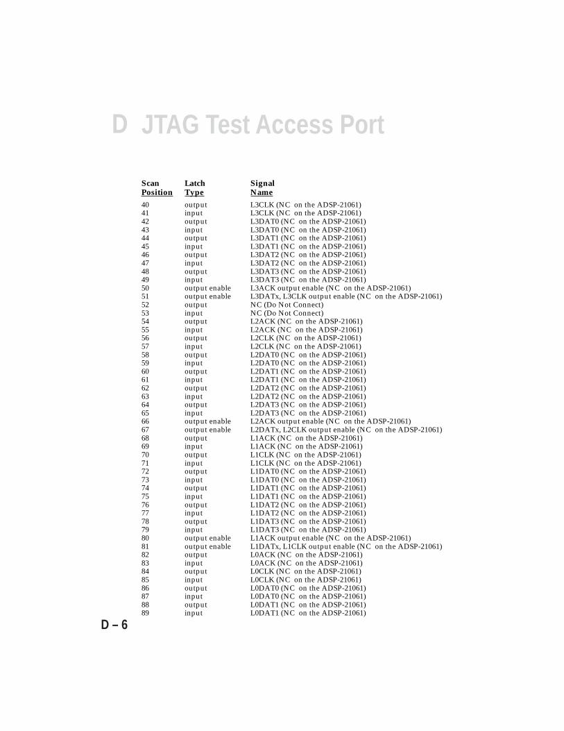
D JTAG Test Access Port
D – 6
Scan Latch SignalPosition Type Name40 output L3CLK (NC on the ADSP-21061)41 input L3CLK (NC on the ADSP-21061)42 output L3DAT0 (NC on the ADSP-21061)43 input L3DAT0 (NC on the ADSP-21061)44 output L3DAT1 (NC on the ADSP-21061)45 input L3DAT1 (NC on the ADSP-21061)46 output L3DAT2 (NC on the ADSP-21061)47 input L3DAT2 (NC on the ADSP-21061)48 output L3DAT3 (NC on the ADSP-21061)49 input L3DAT3 (NC on the ADSP-21061)50 output enable L3ACK output enable (NC on the ADSP-21061)51 output enable L3DATx, L3CLK output enable (NC on the ADSP-21061)52 output NC (Do Not Connect)53 input NC (Do Not Connect)54 output L2ACK (NC on the ADSP-21061)55 input L2ACK (NC on the ADSP-21061)56 output L2CLK (NC on the ADSP-21061)57 input L2CLK (NC on the ADSP-21061)58 output L2DAT0 (NC on the ADSP-21061)59 input L2DAT0 (NC on the ADSP-21061)60 output L2DAT1 (NC on the ADSP-21061)61 input L2DAT1 (NC on the ADSP-21061)62 output L2DAT2 (NC on the ADSP-21061)63 input L2DAT2 (NC on the ADSP-21061)64 output L2DAT3 (NC on the ADSP-21061)65 input L2DAT3 (NC on the ADSP-21061)66 output enable L2ACK output enable (NC on the ADSP-21061)67 output enable L2DATx, L2CLK output enable (NC on the ADSP-21061)68 output L1ACK (NC on the ADSP-21061)69 input L1ACK (NC on the ADSP-21061)70 output L1CLK (NC on the ADSP-21061)71 input L1CLK (NC on the ADSP-21061)72 output L1DAT0 (NC on the ADSP-21061)73 input L1DAT0 (NC on the ADSP-21061)74 output L1DAT1 (NC on the ADSP-21061)75 input L1DAT1 (NC on the ADSP-21061)76 output L1DAT2 (NC on the ADSP-21061)77 input L1DAT2 (NC on the ADSP-21061)78 output L1DAT3 (NC on the ADSP-21061)79 input L1DAT3 (NC on the ADSP-21061)80 output enable L1ACK output enable (NC on the ADSP-21061)81 output enable L1DATx, L1CLK output enable (NC on the ADSP-21061)82 output L0ACK (NC on the ADSP-21061)83 input L0ACK (NC on the ADSP-21061)84 output L0CLK (NC on the ADSP-21061)85 input L0CLK (NC on the ADSP-21061)86 output L0DAT0 (NC on the ADSP-21061)87 input L0DAT0 (NC on the ADSP-21061)88 output L0DAT1 (NC on the ADSP-21061)89 input L0DAT1 (NC on the ADSP-21061)
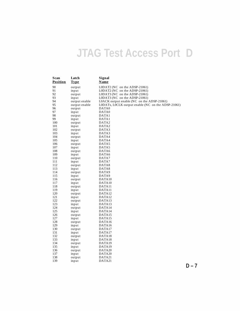
DJTAG Test Access Port
D – 7
Scan Latch SignalPosition Type Name90 output L0DAT2 (NC on the ADSP-21061)91 input L0DAT2 (NC on the ADSP-21061)92 output L0DAT3 (NC on the ADSP-21061)93 input L0DAT3 (NC on the ADSP-21061)94 output enable L0ACK output enable (NC on the ADSP-21061)95 output enable L0DATx, L0CLK output enable (NC on the ADSP-21061)96 output DATA097 input DATA098 output DATA199 input DATA1100 output DATA2101 input DATA2102 output DATA3103 input DATA3104 output DATA4105 input DATA4106 output DATA5107 input DATA5108 output DATA6109 input DATA6110 output DATA7111 input DATA7112 output DATA8113 input DATA8114 output DATA9115 input DATA9116 output DATA10117 input DATA10118 output DATA11119 input DATA11120 output DATA12121 input DATA12122 output DATA13123 input DATA13124 output DATA14125 input DATA14126 output DATA15127 input DATA15128 output DATA16129 input DATA16130 output DATA17131 input DATA17132 output DATA18133 input DATA18134 output DATA19135 input DATA19136 output DATA20137 input DATA20138 output DATA21139 input DATA21
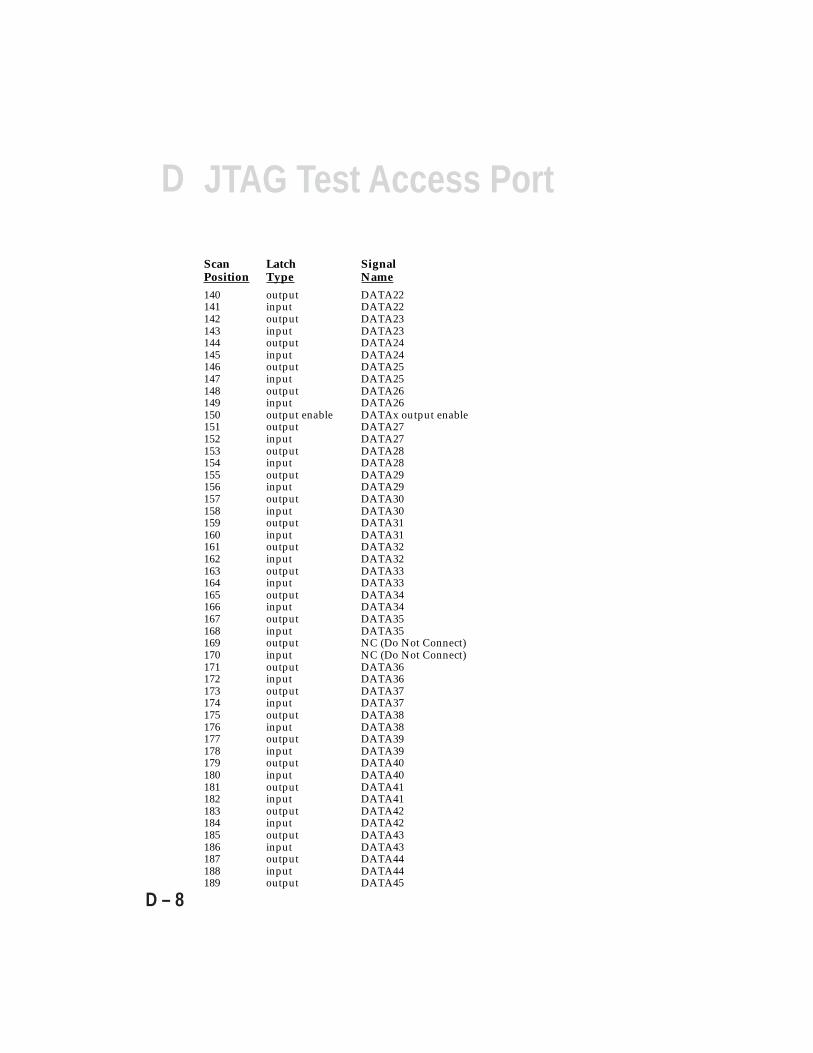
D JTAG Test Access Port
D – 8
Scan Latch SignalPosition Type Name140 output DATA22141 input DATA22142 output DATA23143 input DATA23144 output DATA24145 input DATA24146 output DATA25147 input DATA25148 output DATA26149 input DATA26150 output enable DATAx output enable151 output DATA27152 input DATA27153 output DATA28154 input DATA28155 output DATA29156 input DATA29157 output DATA30158 input DATA30159 output DATA31160 input DATA31161 output DATA32162 input DATA32163 output DATA33164 input DATA33165 output DATA34166 input DATA34167 output DATA35168 input DATA35169 output NC (Do Not Connect)170 input NC (Do Not Connect)171 output DATA36172 input DATA36173 output DATA37174 input DATA37175 output DATA38176 input DATA38177 output DATA39178 input DATA39179 output DATA40180 input DATA40181 output DATA41182 input DATA41183 output DATA42184 input DATA42185 output DATA43186 input DATA43187 output DATA44188 input DATA44189 output DATA45
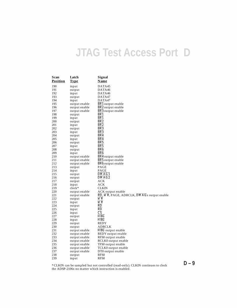
DJTAG Test Access Port
D – 9
Scan Latch SignalPosition Type Name190 input DATA45191 output DATA46192 input DATA46193 output DATA47194 input DATA47195 output enable BR1 output enable196 output enable BR2 output enable197 output enable BR3 output enable198 output BR1199 input BR1200 output BR2201 input BR2202 output BR3203 input BR3204 output BR4205 input BR4206 output BR5207 input BR5208 output BR6209 input BR6210 output enable BR4 output enable211 output enable BR5 output enable212 output enable BR6 output enable213 output PAGE214 input PAGE215 output DMAG1216 output DMAG2217 output ACK218 input ACK219 clock* CLKIN220 output enable ACK output enable221 output enable RD, WR, PAGE, ADRCLK, DMAGx output enable222 output WR223 input WR224 output RD225 input RD226 input CS227 output HBG228 input HBG229 output REDY230 output ADRCLK231 output enable HBG output enable232 output enable REDY output enable233 output enable RFS0 output enable234 output enable RCLK0 output enable235 output enable TFS0 output enable236 output enable TCLK0 output enable237 output enable DT0 output enable238 output RFS0239 input RFS0
* CLKIN can be sampled but not controlled (read-only). CLKIN continues to clockthe ADSP-2106x no matter which instruction is enabled.
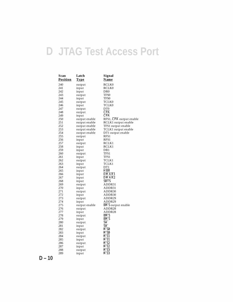
D JTAG Test Access Port
D – 10
Scan Latch SignalPosition Type Name240 output RCLK0241 input RCLK0242 input DR0243 output TFS0244 input TFS0245 output TCLK0246 input TCLK0247 output DT0248 output CPA249 input CPA250 output enable RFS1, CPA output enable251 output enable RCLK1 output enable252 output enable TFS1 output enable253 output enable TCLK1 output enable254 output enable DT1 output enable255 output RFS1256 input RFS1257 output RCLK1258 input RCLK1259 input DR1260 output TFS1261 input TFS1262 output TCLK1263 input TCLK1264 output DT1265 input HBR266 input DMAR1267 input DMAR2268 input SBTS269 output ADDR31270 input ADDR31271 output ADDR30272 input ADDR30273 output ADDR29274 input ADDR29275 output enable BMS output enable276 output ADDR28277 input ADDR28278 output BMS279 input BMS280 output SW281 input SW282 output MS0283 input MS0284 output MS1285 input MS1286 output MS2287 input MS2288 output MS3289 input MS3
DJTAG Test Access Port
D – 11
Scan Latch SignalPosition Type Name290 output ADDR27291 input ADDR27292 output ADDR26293 input ADDR26294 output ADDR25295 input ADDR25296 output ADDR24297 input ADDR24298 output ADDR23299 input ADDR23300 output ADDR22301 input ADDR22302 output ADDR21303 input ADDR21304 output ADDR20305 input ADDR20306 output ADDR19307 input ADDR19308 output enable ADDRx, MSx, SW output enable309 output ADDR18310 input ADDR18311 output ADDR17312 input ADDR17313 output ADDR16314 input ADDR16315 output ADDR15316 input ADDR15317 output ADDR14318 input ADDR14319 output ADDR13320 input ADDR13321 output ADDR12322 input ADDR12323 output ADDR11324 input ADDR11325 output ADDR10326 input ADDR10327 output ADDR9328 input ADDR9329 output ADDR8330 input ADDR8331 output ADDR7332 input ADDR7333 output ADDR6334 input ADDR6335 output ADDR5336 input ADDR5337 output ADDR4338 input ADDR4339 output ADDR3
D JTAG Test Access Port
D – 12
Scan Latch SignalPosition Type Name340 input ADDR3341 output ADDR2342 input ADDR2343 output ADDR1344 input ADDR1345 output ADDR0346 input ADDR0347 output enable FLAG0 output enable348 output enable FLAG1 output enable349 output enable FLAG2 output enable350 output enable FLAG3 output enable351 output FLAG0352 input FLAG0353 output FLAG1354 input FLAG1355 output FLAG2356 input FLAG2357 output FLAG3358 input FLAG3359 output ICSA360 output EMU361 output TIMEXP362 output enable EMU output enable this end closest to TDI
(scan in last)
Output Enables:1 = Drive the associated signals during the EXTEST and INTEST instructions0 = Tristate the associated signals during the EXTEST and INTEST instructions
DJTAG Test Access Port
D – 13
D.5 DEVICE IDENTIFICATION REGISTERNo device identification register is included in the ADSP-2106x.
D.6 BUILT-IN SELF-TEST OPERATION (BIST)No self-test functions are supported by the ADSP-2106x.
D.7 PRIVATE INSTRUCTIONSLoading a value of 001xx into the instruction register enables theprivate instructions reserved for emulation. The ADSP-2106x EZ-ICEemulator uses the TAP and boundary scan as a way to access theprocessor in the target system. The EZ-ICE emulator requires a targetboard connector for access to the TAP. See “EZ-ICE Emulator” inChapter 11, System Design, for information on this connector.
D.8 REFERENCESIEEE Standard 1149.1-1990. Standard Test Access Port and Boundary-Scan Architecture.To order a copy, contact IEEE at 1-800-678-IEEE.
Maunder, C.M. & R. Tulloss. Test Access Ports and Boundary Scan Architectures.IEEE Computer Society Press, 1991.
Parker, Kenneth. The Boundary Scan Handbook.Kluwer Academic Press, 1992.
Bleeker, Harry, P. van den Eijnden, & F. de Jong. Boundary-Scan Test—A Practical Approach.Kluwer Academic Press, 1993.
Hewlett-Packard Co. HP Boundary-Scan Tutorial and BSDL Reference Guide.(HP part# E1017-90001.) 1992.

D JTAG Test Access Port
D – 14
EControl/Status Registers
E – 1
E.1 OVERVIEWThis appendix provides bit definitions for the ADSP-2106x’s control andstatus registers. Some of the registers are located in the processor core;these are called system registers, a subset of the processor’s universalregister set. The core processor system registers are MODE1, MODE2,ASTAT, STKY, IRPTL, IMASK, IMASKP, USTAT1, and USTAT2.
The remaining control registers are located in the ADSP-2106x’s I/OProcessor (IOP). These include the SYSCON and SYSTAT registers. Theseregisters are memory-mapped in ADSP-2106x internal memory.
Register Function Initialization After ResetMODE1 Mode Control 1 0x0000 (cleared)MODE2 Mode Control 2 0xn000 0000 *ASTAT Arithmetic Status 0x00nn 0000 **STKY Sticky Status 0x0540 0000IRPTL Interrupt Latch 0x0000 (cleared)IMASK Interrupt Mask 0x0003IMASKP Interrupt Mask Pointer 0x0000 (cleared)USTAT1 User Status 1 0x0000 (cleared)USTAT2 User Status 2 0x0000 (cleared)
Table E.1 System Registers (Core Processor)* MODE2 bits 28-31 are the processor ID and silicon revision #.** ASTAT bits 19-22 are equal to the values of the FLAG0-3 input pins after reset;the flag pins are configured as inputs after reset
Register Function Initialization After ResetSYSCON System Configuration 0x0000 0010SYSTAT System Status 0x0000 0nn0 *
Table E.2 IOP Registers (I/O Processor)* SYSTAT bits 4-11 depend on the value of the ID2-0 inputs.

E Control/Status Registers
E – 2
All control and status bits are active high unless otherwise noted. Defaultbit values after reset are shown; if no value is shown, the bit is undefinedat reset or depends upon processor inputs. Reserved bits are shown with agray background. Reserved bits must always be written with zeros.
E.2 SYSTEM REGISTERS (CORE PROCESSOR)The system registers of the ADSP-2106x core processor are listed in TableE.1. The system registers are a subset of the universal register set. Theycan be written from an immediate field in an instruction or they can beloaded from or stored to data memory. They can also be transferred to orfrom any other universal register in one cycle.
E.2.1 Effect Latency & Read LatencyA write to any system register other than USTAT1 or USTAT2 has onecycle of latency before any changes are effective. This delay is called effectlatency. Also, if a write to a system register is immediately followed by aread, the value read is always the new one, except for IMASKP whichrequires an extra cycle before the value is updated. This delay is calledread latency.
Effect latency and read latency for the ADSP-2106x system registers arelisted below. A “0” indicates that the write takes effect on the cycleimmediately after the write instruction is executed, and a “1” indicatesone cycle of latency.
Read EffectRegister Contents Latency LatencyMODE1 mode control bits 0 1MODE2 mode control bits 0 1IRPTL interrupt latch 0 1IMASK interrupt mask 0 1IMASKP interrupt mask pointer (for nesting) 1 1ASTAT arithmetic status flags 0 1STKY sticky status flags 0 1USTAT1 user-defined status flags 0 0USTAT2 user-defined status flags 0 0
EControl/Status Registers
E – 3
E.2.2 System Register Bit OperationsThe system register bit manipulation instruction can be used to set, clear,toggle, or test specific bits in the system registers. An immediate field inthe bit manipulation instruction specifies the affected bits. This instructionis described in Appendix A, Instruction Set Reference, Group IV–Miscellaneous.
Examples: BIT SET MODE2 0x00000070;BIT TST ASTAT 0x00002000; result in BTF flag
Although the shifter and ALU have bit manipulation capabilities, thesecomputations operate on register file locations only. System register bitmanipulation instructions eliminate the overhead of transferring systemregisters to and from the register file:
Bit Instruction Shifter Operation(System Registers) (Data Register File)BIT SET register data Rn = BSET Rx BY Ry|dataBIT CLR register data Rn = BCLR Rx BY Ry|dataBIT TGL register data Rn = BTGL Rx BY Ry|dataBIT TST register data BTST Rx BY Ry|data(result in BTF flag) (result in SZ status flag)
E.2.2.1 Bit Test FlagThe test and XOR operations of the system register bit manipulationinstruction store the result in the bit test flag (BTF, bit 18 in the ASTATregister). The state of BTF is a condition that you can use in conditionalinstructions. The test operation sets BTF if all specified bits in the systemregister are set. The XOR operation sets BTF if all bits in the systemregister match the specified bit pattern.
E.2.3 User-Defined Status RegistersTwo undefined 32-bit status registers, USTAT1 and USTAT2, can be user-defined. Bits in these registers can be set and tested using system registerinstructions. You can use these registers for low-overhead, general-purpose software flags or for temporary storage of data.
E Control/Status Registers
E – 4
E.3 IOP REGISTERS (I/O PROCESSOR)The ADSP-2106x’s I/O Processor (IOP) registers are a separate set ofmemory-mapped control and data registers. The IOP registers are usedto configure system-level functions including serial port I/O, link portI/O, and DMA transfers. I/O operations are handled by theADSP-2106x’s on-chip I/O processor, independently from andtransparent to the processor core.
The IOP registers are programmed by writing to the appropriateaddress in memory. They can be programmed by the code executingon the ADSP-2106x core or by an external device such as a hostprocessor or another ADSP-2106x. The symbolic names of the registersand individual bits can be used in ADSP-2106x programs—the#define definitions for these symbols are contained in the filedef21060.h which is provided in the INCLUDE directory of theADSP-21000 Family Development Software. The def21060.h file isshown at the end of this appendix.
E.3.1 IOP Registers SummaryTables E.3, E.4, E.5, and E.6 list the IOP registers used for processorand system control, DMA operations, link port operations, and serialport operations. Table E.7 (on pages 10-13) shows the memory-mappedaddress, functional group, and reset initialization value of each IOPregister.
The memory-mapped IOP registers can be accessed by any externaldevice that is the bus master, either another ADSP-2106x or a hostprocessor. This allows, for example, an external device to set up aDMA transfer to the ADSP-2106x’s internal memory without theADSP-2106x’s intervention. A conflict occurs if both the ADSP-2106xcore processor and the external bus master try to access the same IOPregister group at the same time. In this case, the following rule applies:
When both the ADSP-2106x core processor and the external bus mastersimultaneously attempt to access the same group of IOP registers, the externaldevice always has priority. The ADSP-2106x core will be forced to wait untilthe external device is finished.
Table E.7 shows the different IOP register groups.
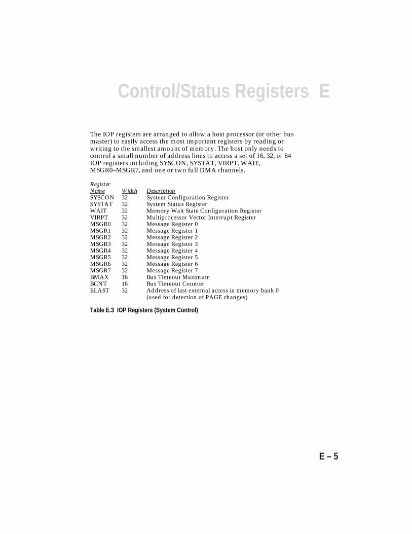
EControl/Status Registers
E – 5
The IOP registers are arranged to allow a host processor (or other busmaster) to easily access the most important registers by reading orwriting to the smallest amount of memory. The host only needs tocontrol a small number of address lines to access a set of 16, 32, or 64IOP registers including SYSCON, SYSTAT, VIRPT, WAIT,MSGR0–MSGR7, and one or two full DMA channels.
RegisterName Width DescriptionSYSCON 32 System Configuration RegisterSYSTAT 32 System Status RegisterWAIT 32 Memory Wait State Configuration RegisterVIRPT 32 Multiprocessor Vector Interrupt RegisterMSGR0 32 Message Register 0MSGR1 32 Message Register 1MSGR2 32 Message Register 2MSGR3 32 Message Register 3MSGR4 32 Message Register 4MSGR5 32 Message Register 5MSGR6 32 Message Register 6MSGR7 32 Message Register 7BMAX 16 Bus Timeout MaximumBCNT 16 Bus Timeout CounterELAST 32 Address of last external access in memory bank 0
(used for detection of PAGE changes)
Table E.3 IOP Registers (System Control)
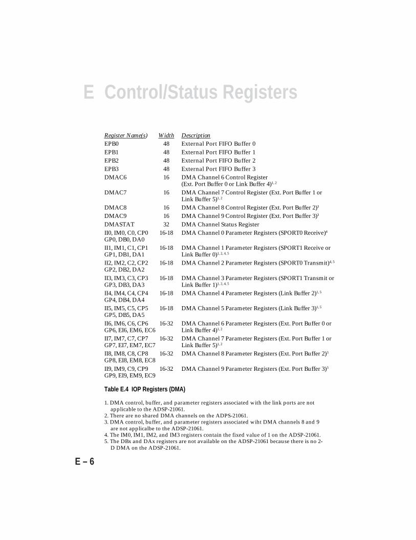
E Control/Status Registers
E – 6
Register Name(s) Width DescriptionEPB0 48 External Port FIFO Buffer 0EPB1 48 External Port FIFO Buffer 1EPB2 48 External Port FIFO Buffer 2EPB3 48 External Port FIFO Buffer 3DMAC6 16 DMA Channel 6 Control Register
(Ext. Port Buffer 0 or Link Buffer 4)1, 2
DMAC7 16 DMA Channel 7 Control Register (Ext. Port Buffer 1 orLink Buffer 5)1, 2
DMAC8 16 DMA Channel 8 Control Register (Ext. Port Buffer 2)3
DMAC9 16 DMA Channel 9 Control Register (Ext. Port Buffer 3)3
DMASTAT 32 DMA Channel Status RegisterII0, IM0, C0, CP0 16-18 DMA Channel 0 Parameter Registers (SPORT0 Receive)4
GP0, DB0, DA0II1, IM1, C1, CP1 16-18 DMA Channel 1 Parameter Registers (SPORT1 Receive orGP1, DB1, DA1 Link Buffer 0)1, 2, 4, 5
II2, IM2, C2, CP2 16-18 DMA Channel 2 Parameter Registers (SPORT0 Transmit)4, 5
GP2, DB2, DA2II3, IM3, C3, CP3 16-18 DMA Channel 3 Parameter Registers (SPORT1 Transmit orGP3, DB3, DA3 Link Buffer 1)1, 2, 4, 5
II4, IM4, C4, CP4 16-18 DMA Channel 4 Parameter Registers (Link Buffer 2)1, 5
GP4, DB4, DA4II5, IM5, C5, CP5 16-18 DMA Channel 5 Parameter Registers (Link Buffer 3)1, 5
GP5, DB5, DA5II6, IM6, C6, CP6 16-32 DMA Channel 6 Parameter Registers (Ext. Port Buffer 0 orGP6, EI6, EM6, EC6 Link Buffer 4)1, 2
II7, IM7, C7, CP7 16-32 DMA Channel 7 Parameter Registers (Ext. Port Buffer 1 orGP7, EI7, EM7, EC7 Link Buffer 5)1, 2
II8, IM8, C8, CP8 16-32 DMA Channel 8 Parameter Registers (Ext. Port Buffer 2)3
GP8, EI8, EM8, EC8II9, IM9, C9, CP9 16-32 DMA Channel 9 Parameter Registers (Ext. Port Buffer 3)3
GP9, EI9, EM9, EC9
Table E.4 IOP Registers (DMA)
1. DMA control, buffer, and parameter registers associated with the link ports are notapplicable to the ADSP-21061.
2. There are no shared DMA channels on the ADPS-21061.3. DMA control, buffer, and parameter registers associated wiht DMA channels 8 and 9
are not applicalbe to the ADSP-21061.4. The IM0, IM1, IM2, and IM3 registers contain the fixed value of 1 on the ADSP-21061.5. The DBx and DAx registers are not available on the ADSP-21061 because there is no 2-
D DMA on the ADSP-21061.

EControl/Status Registers
E – 7
RegisterName Width DescriptionLBUF0 48/32 Link Data Buffer 0LBUF1 48/32 Link Data Buffer 1LBUF2 48/32 Link Data Buffer 2LBUF3 48/32 Link Data Buffer 3LBUF4 48/32 Link Data Buffer 4LBUF5 48/32 Link Data Buffer 5LCTL 32 Link Buffer Control RegisterLCOM 32 Link Common Control RegisterLAR 18 Link Assignment RegisterLSRQ 32 Link Service Request & Mask RegisterLPATH1 32 Link Path 1 Register (Mesh Multiprocessing)LPATH2 32 Link Path 2 Register (Mesh Multiprocessing)LPATH3 32 Link Path 3 Register (Mesh Multiprocessing)LPCNT 32 Link Path Counter (Mesh Multiprocessing)CNST1 40/32 Link Port Constant 1 (Mesh Multiprocessing)CNST2 40/32 Link Port Constant 2 (Mesh Multiprocessing)
Table E.5 IOP Registers (Link Ports)Note: The IOP registers that support the link ports are not available on the ADSP-21061.
RegisterName Width DescriptionSTCTL0 32 SPORT0 Transmit Control RegisterSRCTL0 32 SPORT0 Receive Control RegisterTX0 32 SPORT0 Transmit Data BufferRX0 32 SPORT0 Receive Data BufferTDIV0 32 SPORT0 Transmit DivisorsRDIV0 32 SPORT0 Receive DivisorsMTCS0 32 SPORT0 Multichannel Transmit SelectorMRCS0 32 SPORT0 Multichannel Receive SelectorMTCCS0 32 SPORT0 Multichannel Transmit Compand SelectorMRCCS0 32 SPORT0 Multichannel Receive Compand SelectorSPATH0 16 SPORT0 Path Length (Mesh Multiprocessing)1
KEYWD0 32 SPORT0 Receive Comparison2
KEYMASK0 32 SPORT0 Receive Comparison Mask2
STCTL1 32 SPORT1 Transmit Control RegisterSRCTL1 32 SPORT1 Receive Control RegisterTX1 32 SPORT1 Transmit Data BufferRX1 32 SPORT1 Receive Data BufferTDIV1 32 SPORT1 Transmit DivisorsRDIV1 32 SPORT1 Receive DivisorsMTCS1 32 SPORT1 Multichannel Transmit SelectorMRCS1 32 SPORT1 Multichannel Receive SelectorMTCCS1 32 SPORT1 Multichannel Transmit Compand SelectorMRCCS1 32 SPORT1 Multichannel Receive Compand SelectorSPATH1 16 SPORT1 Path Length (Mesh Multiprocessing)1
KEYWD1 32 SPORT1 Receive Comparison2
KEYMASK1 32 SPORT1 Receive Comparison Mask2
Table E.6 IOP Registers (Serial Ports)1. Not available on the ADSP-21061.2. Only available on the ADSP-21061.
E Control/Status Registers
E – 8
E.3.2 IOP Register Access RestrictionsBecause the IOP registers are memory-mapped they cannot be writtenwith data coming directly from memory. They must instead be writtenfrom (or read into) ADSP-2106x core registers, usually one of thegeneral-purpose registers of the register file (R15–R0). The IOPregisters can also be written or read by external devices, usually otherADSP-2106xs and/or a host processor.
IOP registers other than the DMA buffers cannot be the target of DMAtransfers. During DMA transfers the DMA buffer registers are writtenand read to internal memory over the I/O data bus—these transfersare directly controlled by the ADSP-2106x’s DMA controller, however,not with addresses generated over the I/O address bus. The DMAbuffer registers on the ADSP-21060 and ADSP-21062 include EPB0–EPB3 (external port data buffers), LBUF0–LBUF5 (link port databuffers), and TX0, RX0, TX1, and RX1 (serial port data buffers). On theADSP-21061, the DMA buffer registers include EBP0, EBP1, TX0, RX0,TX1, and RX1.
E.3.3 IOP Register Group Access ContentionThe ADSP-2106x has four separate on-chip buses that canindependently access the memory-mapped IOP registers: the PM bus,DM bus, I/O bus, and external port bus. The external port busconnects the off-chip DATA47-0 bus to all on-chip buses. The I/O busconnects the external port’s data buffers to memory and to the on-chipI/O processor. The I/O bus carries data being transferred to and fromthe DMA buffer IOP registers.
Any of these buses can attempt to read or write an IOP register at anytime. Access contention occurs when more than one of the busesattempts to access the same group of IOP registers (see Table E.7). Oneexception to this access contention rule exists: the I/O bus and externalport bus can simultaneously access the DB (DMA buffer) group ofregisters, allowing DMA transfers to internal memory at full speed.
IOP register group access conflicts are resolved on a fixed prioritybasis. External port to IOP register accesses occur first, thenPM and/or DM bus, then I/O bus:
External port ↔ IOP register accesses 1st priorityPM-DM bus ↔ IOP register accesses 2nd priority
EControl/Status Registers
E – 9
I/O bus ↔ IOP register accesses 3rd priority
The bus with the highest priority will gain access to the IOP registersfirst and any lower priority accesses are held off (by extra cyclesgenerated by the core processor and/or I/O processor). If a DMAgrant has been given for an I/O access, that access will be completedbefore an access from any another bus is allowed.
The external port DMA data buffers (EPB0–EPB3) are 6-word deepFIFOs. An input to the buffers can occur in the same cycle as anoutput. The external port bus has its own independent access to thesebuffers. Contention occurs when the PM bus, DM bus, and/or I/O bustry to access the data buffers at the same time. In this case the I/O busaccess proceeds first, but subsequent I/O bus accesses are held offuntil after the PM and/or DM bus accesses.
E.3.4 IOP Register Write LatenciesIOP register writes are internally completed at the end of the cycle inwhich they occur. The IOP register will therefore read back the newlywritten value on the very next cycle.
Not all writes take effect in the next cycle, however. Control and modebits generally take effect in the second cycle after completion of thewrite, with the exception of the external port packing control bits andbuffer flush bits which take effect in the third cycle after completion ofthe write.
The external port and core processor may conflict if they attempt toaccess the same IOP register group. In this case the core processoraccess is delayed until all external port accesses have completed.
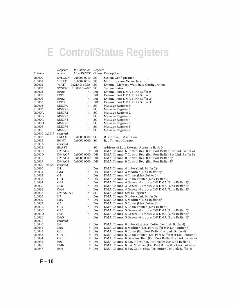
E Control/Status Registers
E – 10
Register Initialization RegisterAddress Name After RESET Group Description0x0000 SYSCON 0x0000 0010 SC System Configuration0x0001 VIRPT 0x0002 0014 SC Multiprocessor Vector Interrupt0x0002 WAIT 0x21AD 6B5A SC External Memory Wait State Configuration0x0003 SYSTAT 0x0000 0nn0 * SC System Status0x0004 EPB0 ni DB External Port DMA FIFO Buffer 00x0005 EPB1 ni DB External Port DMA FIFO Buffer 10x0006 EPB2 ni DB External Port DMA FIFO Buffer 21
0x0007 EPB3 ni DB External Port DMA FIFO Buffer 31
0x0008 MSGR0 ni SC Message Register 00x0009 MSGR1 ni SC Message Register 10x000A MSGR2 ni SC Message Register 20x000B MSGR3 ni SC Message Register 30x000C MSGR4 ni SC Message Register 40x000D MSGR5 ni SC Message Register 50x000E MSGR6 ni SC Message Register 60x000F MSGR7 ni SC Message Register 70x0010–0x0017 reserved0x0018 BMAX 0x0000 0000 SC Bus Timeout Maximum0x0019 BCNT 0x0000 0000 SC Bus Timeout Counter0x001A reserved0x001B ELAST ni SC Address of Last External Access in Bank 00x001C DMAC6 † DB DMA Channel 6 Control Reg. (Ext. Port Buffer 0 or Link Buffer 4)0x001D DMAC7 0x0000 0000 DB DMA Channel 7 Control Reg. (Ext. Port Buffer 1 or Link Buffer 5)0x001E DMAC8 0x0000 0000 DB DMA Channel 8 Control Reg. (Ext. Port Buffer 2)1
0x001F DMAC9 0x0000 0000 DB DMA Channel 9 Control Reg. (Ext. Port Buffer 3)1
0x0020–0x002F reserved0x0030 II4 ni DA DMA Channel 4 Index (Link Buffer 2)1
0x0031 IM4 ni DA DMA Channel 4 Modifier (Link Buffer 2)1
0x0032 C4 ni DA DMA Channel 4 Count (Link Buffer 2)1
0x0033 CP4 ni DA DMA Channel 4 Chain Pointer (Link Buffer 2)1
0x0034 GP4 ni DA DMA Channel 4 General-Purpose/2-D DMA (Link Buffer 2)1
0x0035 DB4 ni DA DMA Channel 4 General-Purpose/2-D DMA (Link Buffer 2)1
0x0036 DA4 ni DA DMA Channel 4 General-Purpose/2-D DMA (Link Buffer 2)1
0x0037 DMASTAT ni SC DMA Channel Status Register0x0038 II5 ni DA DMA Channel 5 Index (Link Buffer 3)1
0x0039 IM5 ni DA DMA Channel 5 Modifier (Link Buffer 3)1
0x003A C5 ni DA DMA Channel 5 Count (Link Buffer 3)1
0x003B CP5 ni DA DMA Channel 5 Chain Pointer (Link Buffer 3)1
0x003C GP5 ni DA DMA Channel 5 General-Purpose/2-D DMA (Link Buffer 3)1
0x003D DB5 ni DA DMA Channel 5 General-Purpose/2-D DMA (Link Buffer 3)1
0x003E DA5 ni DA DMA Channel 5 General-Purpose/2-D DMA (Link Buffer 3)1
0x003F reserved0x0040 II6 † DA DMA Channel 6 Index (Ext. Port Buffer 0 or Link Buffer 4)0x0041 IM6 † DA DMA Channel 6 Modifier (Ext. Port Buffer 0 or Link Buffer 4)0x0042 C6 † DA DMA Channel 6 Count (Ext. Port Buffer 0 or Link Buffer 4)0x0043 CP6 † DA DMA Channel 6 Chain Pointer (Ext. Port Buffer 0 or Link Buffer 4)0x0044 GP6 † DA DMA Channel 6 Gen-Pur. Reg. (Ext. Port Buffer 0 or Link Buffer 4)0x0045 EI6 † DA DMA Channel 6 Ext. Index (Ext. Port Buffer 0 or Link Buffer 4)0x0046 EM6 † DA DMA Channel 6 Ext. Modifier (Ext. Port Buffer 0 or Link Buffer 4)0x0047 EC6 † DA DMA Channel 6 Ext. Count (Ext. Port Buffer 0 or Link Buffer 4)
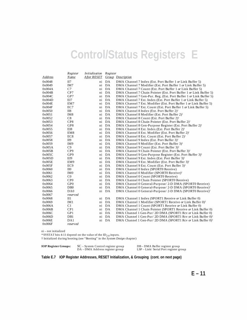
EControl/Status Registers
E – 11
Register Initialization RegisterAddress Name After RESET Group Description0x0048 II7 ni DA DMA Channel 7 Index (Ext. Port Buffer 1 or Link Buffer 5)0x0049 IM7 ni DA DMA Channel 7 Modifier (Ext. Port Buffer 1 or Link Buffer 5)0x004A C7 ni DA DMA Channel 7 Count (Ext. Port Buffer 1 or Link Buffer 5)0x004B CP7 ni DA DMA Channel 7 Chain Pointer (Ext. Port Buffer 1 or Link Buffer 5)0x004C GP7 ni DA DMA Channel 7 Gen-Pur. Reg. (Ext. Port Buffer 1 or Link Buffer 5)0x004D EI7 ni DA DMA Channel 7 Ext. Index (Ext. Port Buffer 1 or Link Buffer 5)0x004E EM7 ni DA DMA Channel 7 Ext. Modifier (Ext. Port Buffer 1 or Link Buffer 5)0x004F EC7 ni DA DMA Channel 7 Ext. Count (Ext. Port Buffer 1 or Link Buffer 5)0x0050 II8 ni DA DMA Channel 8 Index (Ext. Port Buffer 2)1
0x0051 IM8 ni DA DMA Channel 8 Modifier (Ext. Port Buffer 2)1
0x0052 C8 ni DA DMA Channel 8 Count (Ext. Port Buffer 2)1
0x0053 CP8 ni DA DMA Channel 8 Chain Pointer (Ext. Port Buffer 2)1
0x0054 GP8 ni DA DMA Channel 8 Gen-Purpose Register (Ext. Port Buffer 2)1
0x0055 EI8 ni DA DMA Channel 8 Ext. Index (Ext. Port Buffer 2)1
0x0056 EM8 ni DA DMA Channel 8 Ext. Modifier (Ext. Port Buffer 2)1
0x0057 EC8 ni DA DMA Channel 8 Ext. Count (Ext. Port Buffer 2)1
0x0058 II9 ni DA DMA Channel 9 Index (Ext. Port Buffer 3)1
0x0059 IM9 ni DA DMA Channel 9 Modifier (Ext. Port Buffer 3)1
0x005A C9 ni DA DMA Channel 9 Count (Ext. Port Buffer 3)1
0x005B CP9 ni DA DMA Channel 9 Chain Pointer (Ext. Port Buffer 3)1
0x005C GP9 ni DA DMA Channel 9 Gen-Purpose Register (Ext. Port Buffer 3)1
0x005D EI9 ni DA DMA Channel 9 Ext. Index (Ext. Port Buffer 3)1
0x005E EM9 ni DA DMA Channel 9 Ext. Modifier (Ext. Port Buffer 3)1
0x005F EC9 ni DA DMA Channel 9 Ext. Count (Ext. Port Buffer 3)1
0x0060 II0 ni DA DMA Channel 0 Index (SPORT0 Receive)0x0061 IM0 ni DA DMA Channel 0 Modifier (SPORT0 Receive)2
0x0062 C0 ni DA DMA Channel 0 Count (SPORT0 Receive)0x0063 CP0 ni DA DMA Channel 0 Chain Pointer (SPORT0 Receive)0x0064 GP0 ni DA DMA Channel 0 General-Purpose/2-D DMA (SPORT0 Receive)0x0065 DB0 ni DA DMA Channel 0 General-Purpose/2-D DMA (SPORT0 Receive)1
0x0066 DA0 ni DA DMA Channel 0 General-Purpose/2-D DMA (SPORT0 Receive)1
0x0067 reserved0x0068 II1 ni DA DMA Channel 1 Index (SPORT1 Receive or Link Buffer 0)0x0069 IM1 ni DA DMA Channel 1 Modifier (SPORT1 Receive or Link Buffer 0)2
0x006A C1 ni DA DMA Channel 1 Count (SPORT1 Receive or Link Buffer 0)0x006B CP1 ni DA DMA Channel 1 Chain Pointer (SPORT1 Receive or Link Buffer 0)0x006C GP1 ni DA DMA Channel 1 Gen-Pur/2D DMA (SPORT1 Rcv or Link Buffer 0)0x006D DB1 ni DA DMA Channel 1 Gen-Pur/2D DMA (SPORT1 Rcv or Link Buffer 0)1
0x006E DA1 ni DA DMA Channel 1 Gen-Pur/2D DMA (SPORT1 Rcv or Link Buffer 0)1
0x006F reserved
ni – not initialized* SYSTAT bits 4-11 depend on the value of the ID2-0 inputs.† Initialized during booting (see “Booting” in the System Design chapter)
IOP Register Groups: SC – System Control register group DB – DMA Buffer register groupDA – DMA Address register group LSP – Link/Serial Port register group
Table E.7 IOP Register Addresses, RESET Initialization, & Grouping (cont. on next page)

E Control/Status Registers
E – 12
Register Initialization RegisterAddress Name After RESET Group Description0x0070 II2 ni DA DMA Channel 2 Index (SPORT0 Transmit)0x0071 IM2 ni DA DMA Channel 2 Modifier (SPORT0 Transmit)2
0x0072 C2 ni DA DMA Channel 2 Count (SPORT0 Transmit)0x0073 CP2 ni DA DMA Channel 2 Chain Pointer (SPORT0 Transmit)0x0074 GP2 ni DA DMA Channel 2 Gen-Pur/2D DMA (SPORT0 Transmit)0x0075 DB2 ni DA DMA Channel 2 Gen-Pur/2D DMA (SPORT0 Transmit)1
0x0076 DA2 ni DA DMA Channel 2 Gen-Pur/2D DMA (SPORT0 Transmit)1
0x0077 reserved0x0078 II3 ni DA DMA Channel 3 Index (SPORT1 Transmit or Link Buffer 1)0x0079 IM3 ni DA DMA Channel 3 Modifier (SPORT1 Transmit or Link Buffer 1)2
0x007A C3 ni DA DMA Channel 3 Count (SPORT1 Transmit or Link Buffer 1)0x007B CP3 ni DA DMA Channel 3 Chain Pointer (SPORT1 Transmit or Link Buffer 1)0x007C GP3 ni DA DMA Channel 3 Gen-Pur/2D DMA (SPORT1 Transmit or Link Buffer 1)0x007D DB3 ni DA DMA Channel 3 Gen-Pur/2D DMA (SPORT1 Transmit or Link Buffer 1)1
0x007E DA3 ni DA DMA Channel 3 Gen-Pur/2D DMA (SPORT1 Transmit or Link Buffer 1)1
0x007F reserved0x00A0–0x00BF reserved0x00C0 LBUF0 ni LSP Link Buffer 01
0x00C1 LBUF1 ni LSP Link Buffer 11
0x00C2 LBUF2 ni LSP Link Buffer 21
0x00C3 LBUF3 ni LSP Link Buffer 31
0x00C4 LBUF4 ni LSP Link Buffer 41
0x00C5 LBUF5 ni LSP Link Buffer 51
0x00C6 LCTL 0x0000 0000 LSP Link Buffer Control Register1
0x00C7 LCOM 0x0000 0000 LSP Link Common Control Register1
0x00C8 LAR 0x2C688 LSP Link Buffer Assignment Register1
0x00C9 LSRQ 0x0000 0000 LSP Link Port Service Request & Mask Register1
0x00CA LPATH1 ni LSP Link Path 1 Register (Mesh Multiprocessing)1
0x00CB LPATH2 ni LSP Link Path 2 Register (Mesh Multiprocessing)1
0x00CC LPATH3 ni LSP Link Path 3 Register (Mesh Multiprocessing)1
0x00CD LPCNT ni LSP Link Path Counter (Mesh Multiprocessing)1
0x00CE CNST1 ni LSP Link Port Constant 1 (Mesh Multiprocessing)1
0x00CF CNST2 ni LSP Link Port Constant 2 (Mesh Multiprocessing)1
0x00D0–0x00DF reserved0x00E0 STCTL0 0x0000 0000 LSP SPORT0 Transmit Control Register0x00E1 SRCTL0 0x0000 0000 LSP SPORT0 Receive Control Register0x00E2 TX0 ni LSP SPORT0 Transmit Data Buffer0x00E3 RX0 ni LSP SPORT0 Receive Data Buffer0x00E4 TDIV0 ni LSP SPORT0 Transmit Divisors0x00E5 reserved0x00E6 RDIV0 ni LSP SPORT0 Receive Divisors0x00E7 reserved0x00E8 MTCS0 ni LSP SPORT0 Multichannel Transmit Selector0x00E9 MRCS0 ni LSP SPORT0 Multichannel Receive Selector0x00EA MTCCS0 ni LSP SPORT0 Multichannel Transmit Compand Selector0x00EB MRCCS0 ni LSP SPORT0 Multichannel Receive Compand Selector0x00EC KEYWD0 ni LSP SPORT0 Receive Comparison3
0x00ED KEYMASK0 ni LSP SPORT0 Receive Comparison Mask3
0x00EE SPATH0 0x0001 LSP SPORT0 Path Length (Mesh Multiprocessing)0x00EF reserved 0x0001

EControl/Status Registers
E – 13
Register Initialization RegisterAddress Name After RESET Group Description0x00F0 STCTL1 0x0000 0000 LSP SPORT1 Transmit Control Register0x00F1 SRCTL1 0x0000 0000 LSP SPORT1 Receive Control Register0x00F2 TX1 ni LSP SPORT1 Transmit Data Buffer0x00F3 RX1 ni LSP SPORT1 Receive Data Buffer0x00F4 TDIV1 ni LSP SPORT1 Transmit Divisors0x00F5 reserved0x00F6 RDIV1 ni LSP SPORT1 Receive Divisors0x00F7 reserved0x00F8 MTCS1 ni LSP SPORT1 Multichannel Transmit Selector0x00F9 MRCS1 ni LSP SPORT1 Multichannel Receive Selector0x00FA MTCCS1 ni LSP SPORT1 Multichannel Transmit Compand Selector0x00FB MRCCS1 ni LSP SPORT1 Multichannel Receive Compand Selector0x00FC KEYWD1 ni LSP SPORT1 Receive Comparison3
0x00FD KEYMASK1 ni LSP SPORT1 Receive Comparison Mask3
0x00FE SPATH1 0x0001 LSP SPORT1 Path Length (Mesh Multiprocessing)0x00FF reserved 0x0001
ni – not initialized
IOP Register Groups: SC – System Control register group DB – DMA Buffer register groupDA – DMA Address register group LSP – Link/Serial Port register group
Table E.7 IOP Register Addresses, RESET Initialization, & Grouping (cont.)
1. Not available on the ADSP-21061.2. The contents of the IM0-3 registers are fixed to ‘1’ on the ADSP-21061; on this DSP,
these registers may be written, but the writes are ignored and reads of theseregisters return the value ‘1.’
3. Only available on the ADSP-21061. This register location is reserved on the ADSP-21060 and ADSP-21062.
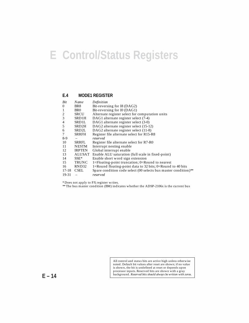
E Control/Status Registers
E – 14
E.4 MODE1 REGISTERBit Name Definition0 BR8 Bit-reversing for I8 (DAG2)1 BR0 Bit-reversing for I0 (DAG1)2 SRCU Alternate register select for computation units3 SRD1H DAG1 alternate register select (7-4)4 SRD1L DAG1 alternate register select (3-0)5 SRD2H DAG2 alternate register select (15-12)6 SRD2L DAG2 alternate register select (11-8)7 SRRFH Register file alternate select for R15-R88-9 – reserved10 SRRFL Register file alternate select for R7-R011 NESTM Interrupt nesting enable12 IRPTEN Global interrupt enable13 ALUSAT Enable ALU saturation (full scale in fixed-point)14 SSE* Enable short word sign extension15 TRUNC 1=Floating-point truncation; 0=Round to nearest16 RND32 1=Round floating-point data to 32 bits; 0=Round to 40 bits17-18 CSEL Spare condition code select (00 selects bus master condition)**19-31 – reserved
* Does not apply to PX register writes.** The bus master condition (BM) indicates whether the ADSP-2106x is the current bus
All control and status bits are active high unless otherwisenoted. Default bit values after reset are shown; if no valueis shown, the bit is undefined at reset or depends uponprocessor inputs. Reserved bits are shown with a graybackground. Reserved bits should always be written with zeros.
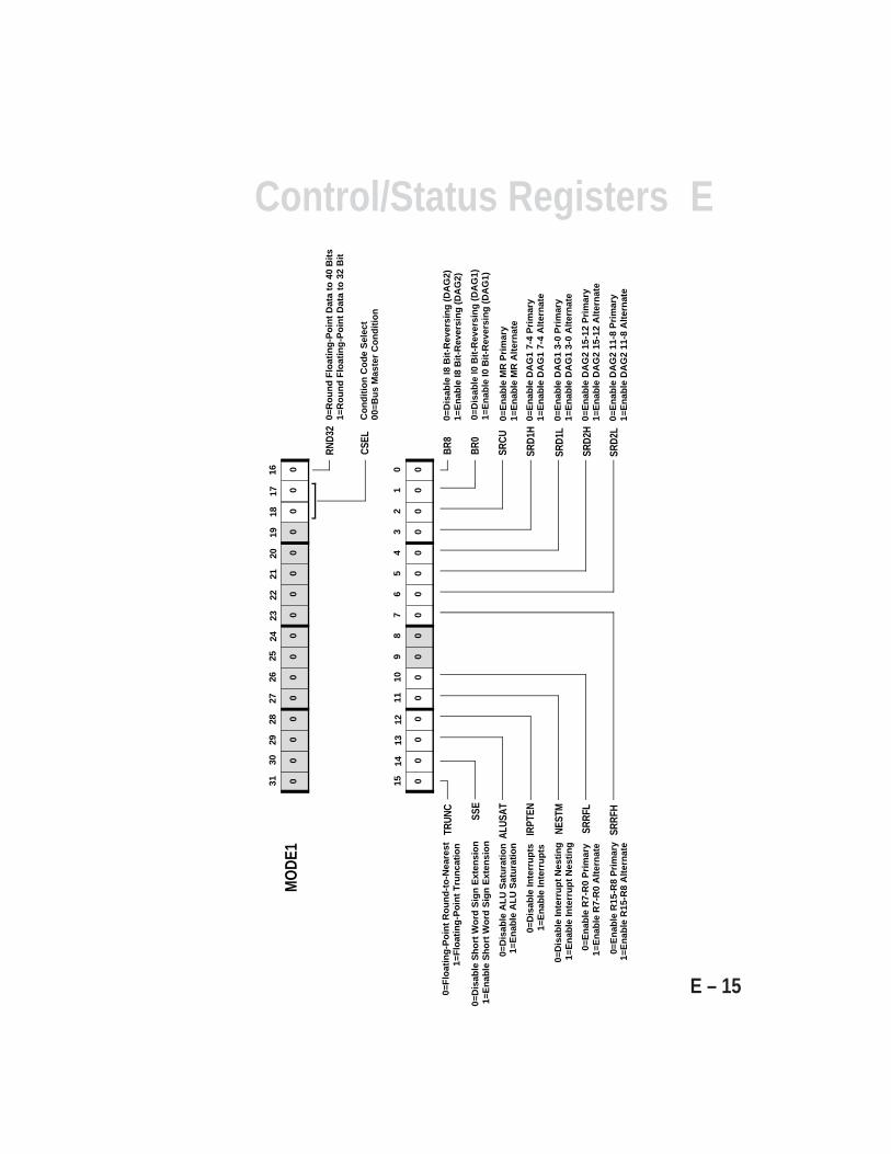
EControl/Status Registers
E – 15
1110
98
76
54
32
10
0=D
isab
le A
LU
Sat
ura
tio
n1=
En
able
AL
U S
atu
rati
on
0=F
loat
ing
-Po
int
Ro
un
d-t
o-N
eare
st1=
Flo
atin
g-P
oin
t T
run
cati
on
0=R
ou
nd
Flo
atin
g-P
oin
t D
ata
to 4
0 B
its
1=R
ou
nd
Flo
atin
g-P
oin
t D
ata
to 3
2 B
it
00
00
00
00
00
00
1514
1312 0
00
0
0=D
isab
le In
terr
up
ts1=
En
able
Inte
rru
pts
0=D
isab
le In
terr
up
t N
esti
ng
1=E
nab
le In
terr
up
t N
esti
ng
0=E
nab
le R
7-R
0 P
rim
ary
1=E
nab
le R
7-R
0 A
lter
nat
e
0=E
nab
le R
15-R
8 P
rim
ary
1=E
nab
le R
15-R
8 A
lter
nat
e0=
En
able
DA
G2
11-8
Pri
mar
y1=
En
able
DA
G2
11-8
Alt
ern
ate
0=E
nab
le D
AG
2 15
-12
Pri
mar
y1=
En
able
DA
G2
15-1
2 A
lter
nat
e
0=E
nab
le D
AG
1 3-
0 P
rim
ary
1=E
nab
le D
AG
1 3-
0 A
lter
nat
e
0=E
nab
le D
AG
1 7-
4 P
rim
ary
1=E
nab
le D
AG
1 7-
4 A
lter
nat
e
0=E
nab
le M
R P
rim
ary
1=E
nab
le M
R A
lter
nat
e
0=D
isab
le I0
Bit
-Rev
ersi
ng
(D
AG
1)1=
En
able
I0 B
it-R
ever
sin
g (
DA
G1)
2625
2423
2221
2019
1817
00
00
00
00
00
00
3130
2928
27
00
00
16
BR
0
SRC
U
SRD1
H
SRD1
L
SRD2
H
SRD2
LSR
RFH
SRRF
L
NEST
M
IRPT
EN
ALUS
AT
TRUN
C
RND3
2
0=D
isab
le I8
Bit
-Rev
ersi
ng
(D
AG
2)1=
En
able
I8 B
it-R
ever
sin
g (
DA
G2)
BR
8
0=D
isab
le S
ho
rt W
ord
Sig
n E
xten
sio
n1=
En
able
Sh
ort
Wo
rd S
ign
Ext
ensi
on
SSE
Co
nd
itio
n C
od
e S
elec
t00
=Bu
s M
aste
r C
on
dit
ion
CSEL
MO
DE1
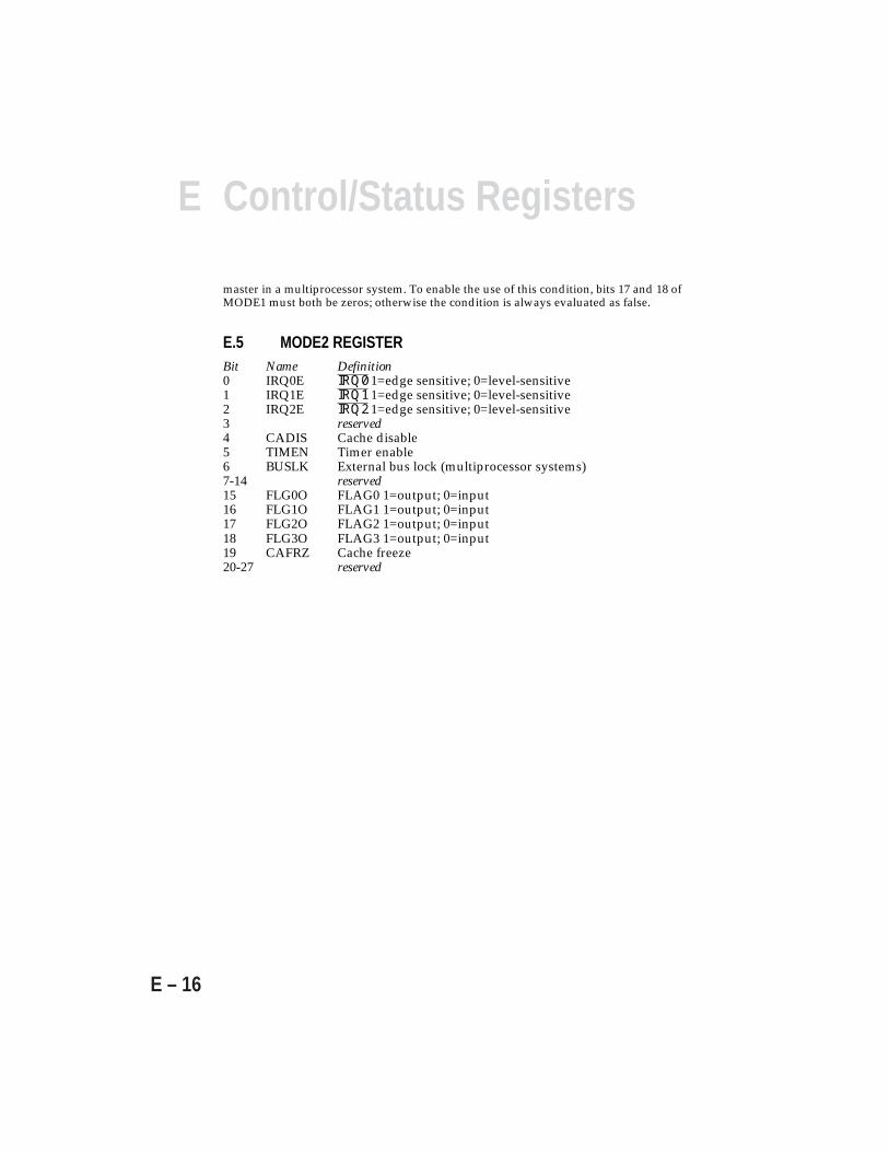
E Control/Status Registers
E – 16
master in a multiprocessor system. To enable the use of this condition, bits 17 and 18 ofMODE1 must both be zeros; otherwise the condition is always evaluated as false.
E.5 MODE2 REGISTERBit Name Definition0 IRQ0E IRQ0 1=edge sensitive; 0=level-sensitive1 IRQ1E IRQ1 1=edge sensitive; 0=level-sensitive2 IRQ2E IRQ2 1=edge sensitive; 0=level-sensitive3 reserved4 CADIS Cache disable5 TIMEN Timer enable6 BUSLK External bus lock (multiprocessor systems)7-14 reserved15 FLG0O FLAG0 1=output; 0=input16 FLG1O FLAG1 1=output; 0=input17 FLG2O FLAG2 1=output; 0=input18 FLG3O FLAG3 1=output; 0=input19 CAFRZ Cache freeze20-27 reserved
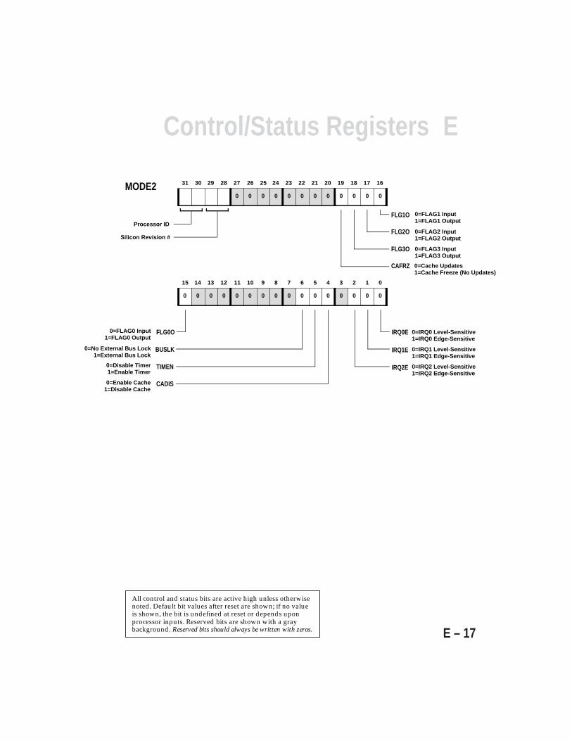
EControl/Status Registers
E – 17
11 10 9 8 7 6 5 4 3 2 1 0
000000000000
15 14 13 12
0000
0=Disable Timer1=Enable Timer
0=Enable Cache1=Disable Cache
26 25 24 23 22 21 20 19 18 17
000000000000
31 30 29 28 27 16
0=IRQ0 Level-Sensitive1=IRQ0 Edge-Sensitive
0=IRQ1 Level-Sensitive1=IRQ1 Edge-Sensitive
0=IRQ2 Level-Sensitive1=IRQ2 Edge-Sensitive
0=No External Bus Lock1=External Bus Lock
0=Cache Updates1=Cache Freeze (No Updates)
0=FLAG1 Input1=FLAG1 Output
0=FLAG2 Input1=FLAG2 Output
IRQ0E
IRQ1E
IRQ2E
BUSLK
TIMEN
CADIS
FLG1O
FLG2O
CAFRZ
Silicon Revision #
0=FLAG0 Input1=FLAG0 Output
FLG0O
0=FLAG3 Input1=FLAG3 Output
FLG3O
Processor ID
All control and status bits are active high unless otherwisenoted. Default bit values after reset are shown; if no valueis shown, the bit is undefined at reset or depends uponprocessor inputs. Reserved bits are shown with a graybackground. Reserved bits should always be written with zeros.
MODE2
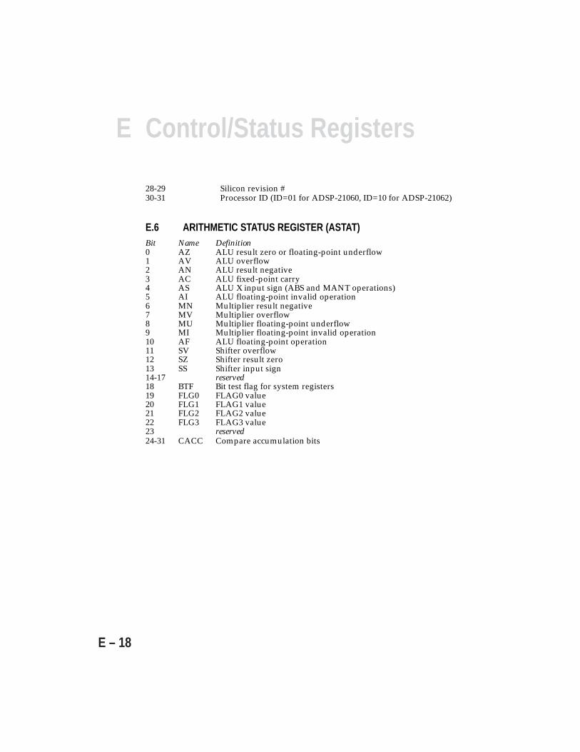
E Control/Status Registers
E – 18
28-29 Silicon revision #30-31 Processor ID (ID=01 for ADSP-21060, ID=10 for ADSP-21062)
E.6 ARITHMETIC STATUS REGISTER (ASTAT)Bit Name Definition0 AZ ALU result zero or floating-point underflow1 AV ALU overflow2 AN ALU result negative3 AC ALU fixed-point carry4 AS ALU X input sign (ABS and MANT operations)5 AI ALU floating-point invalid operation6 MN Multiplier result negative7 MV Multiplier overflow8 MU Multiplier floating-point underflow9 MI Multiplier floating-point invalid operation10 AF ALU floating-point operation11 SV Shifter overflow12 SZ Shifter result zero13 SS Shifter input sign14-17 reserved18 BTF Bit test flag for system registers19 FLG0 FLAG0 value20 FLG1 FLAG1 value21 FLG2 FLAG2 value22 FLG3 FLAG3 value23 reserved24-31 CACC Compare accumulation bits

EControl/Status Registers
E – 19
11 10 9 8 7 6 5 4 3 2 1 0
Bit Test Flag for System Registers
000000000000
15 14 13 12
0000
ALU Floating-Point Invalid Operation
ALU X-Input Sign (for ABS and MANT)
ALU Fixed-Point Carry
ALU Negative
ALU Overflow
26 25 24 23 22 21 20 19 18 17
00000000
31 30 29 28 27
0000
16
ALU Zero/Floating-Point Underflow
Multiplier Floating-Point Invalid Operation
Multiplier NegativeMultiplier Overflow
Multiplier Floating-Point Underflow
ALU Floating-Point Operation
Shifter Input Sign
Shifter Overflow
Shifter Zero
FLAG0 Value
FLAG1 Value
FLAG3 Value
FLAG2 Value
Compare Accumulation Shift RegisterCACC
AZ
AV
AN
AC
AS
AI
MN
SS
SZ
SV
AF
MI
MU
MV
BTF
FLG0
FLG1
FLG3
FLG2
All control and status bits are active high unless otherwisenoted. Default bit values after reset are shown; if no valueis shown, the bit is undefined at reset or depends uponprocessor inputs. Reserved bits are shown with a graybackground. Reserved bits should always be written with zeros.
ASTAT
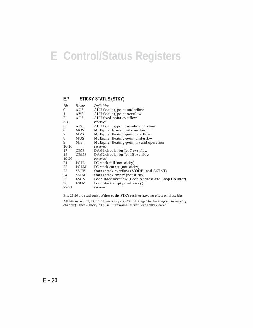
E Control/Status Registers
E – 20
E.7 STICKY STATUS (STKY)Bit Name Definition0 AUS ALU floating-point underflow1 AVS ALU floating-point overflow2 AOS ALU fixed-point overflow3-4 reserved5 AIS ALU floating-point invalid operation6 MOS Multiplier fixed-point overflow7 MVS Multiplier floating-point overflow8 MUS Multiplier floating-point underflow9 MIS Multiplier floating-point invalid operation10-16 reserved17 CB7S DAG1 circular buffer 7 overflow18 CB15S DAG2 circular buffer 15 overflow19-20 reserved21 PCFL PC stack full (not sticky)22 PCEM PC stack empty (not sticky)23 SSOV Status stack overflow (MODE1 and ASTAT)24 SSEM Status stack empty (not sticky)25 LSOV Loop stack overflow (Loop Address and Loop Counter)26 LSEM Loop stack empty (not sticky)27-31 reserved
Bits 21-26 are read-only. Writes to the STKY register have no effect on these bits.
All bits except 21, 22, 24, 26 are sticky (see “Stack Flags” in the Program Sequencingchapter). Once a sticky bit is set, it remains set until explicitly cleared.
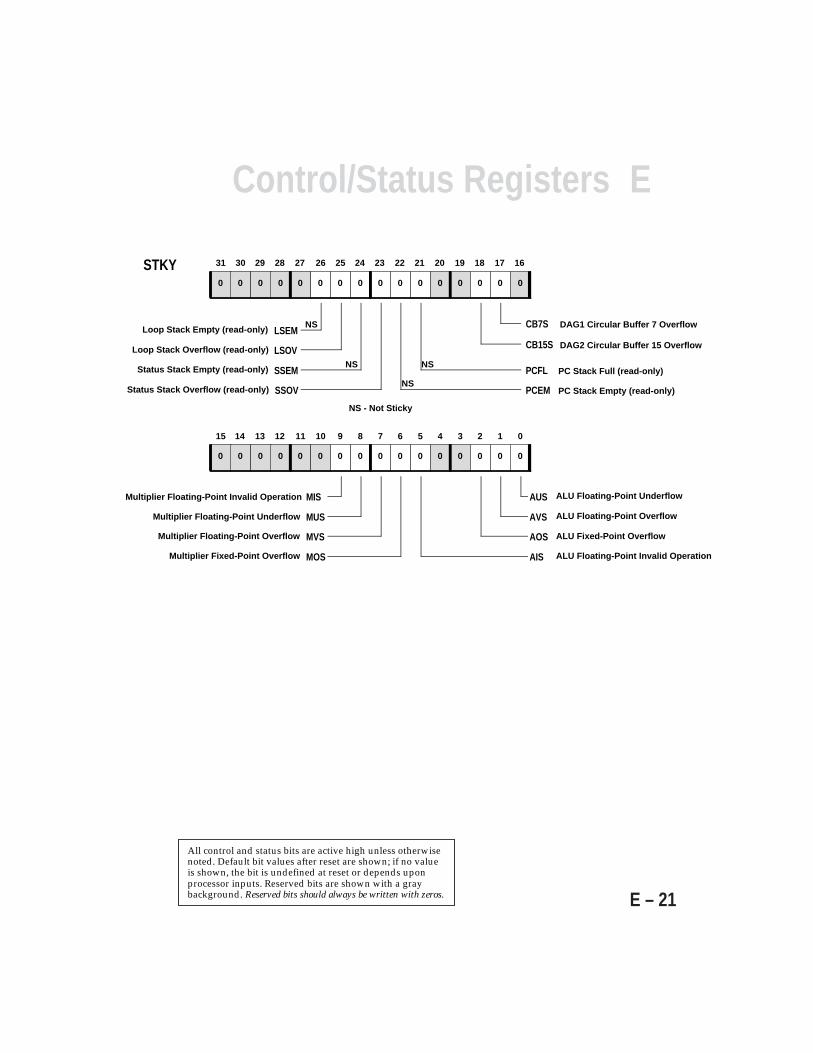
EControl/Status Registers
E – 21
AUS
AVS
AOS
AIS
11 10 9 8 7 6 5 4 3 2 1 0
DAG1 Circular Buffer 7 Overflow
000000000000
15 14 13 12
0000
ALU Floating-Point Invalid Operation
ALU Fixed-Point Overflow
ALU Floating-Point Overflow
26 25 24 23 22 21 20 19 18 17
000000000000
31 30 29 28 27
0000
16
ALU Floating-Point UnderflowMultiplier Floating-Point Invalid Operation
Multiplier Floating-Point Overflow
Multiplier Floating-Point Underflow
Status Stack Empty (read-only)
Status Stack Overflow (read-only)
Multiplier Fixed-Point Overflow
DAG2 Circular Buffer 15 Overflow
PC Stack Empty (read-only)
PC Stack Full (read-only)
Loop Stack Empty (read-only)
Loop Stack Overflow (read-only)
MIS
MUS
MVS
MOS
CB7S
CB15S
PCFL
PCEM
LSEM
LSOV
SSEM
SSOV
NS - Not Sticky
NS
NS
NS
NS
All control and status bits are active high unless otherwisenoted. Default bit values after reset are shown; if no valueis shown, the bit is undefined at reset or depends uponprocessor inputs. Reserved bits are shown with a graybackground. Reserved bits should always be written with zeros.
STKY
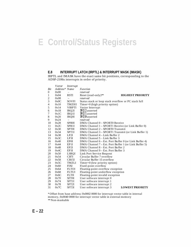
E Control/Status Registers
E – 22
E.8 INTERRUPT LATCH (IRPTL) & INTERRUPT MASK (IMASK)IRPTL and IMASK have the exact same bit positions, corresponding to theADSP-2106x interrupts in order of priority.
Vector InterruptBit Address* Name Function0 0x00 – reserved1 0x04 RSTI Reset (read-only)** HIGHEST PRIORITY2 0x08 – reserved3 0x0C SOVFI Status stack or loop stack overflow or PC stack full4 0x10 TMZHI Timer=0 (high priority option)5 0x14 VIRPTI Vector Interrupt6 0x18 IRQ2I IRQ2 asserted7 0x1C IRQ1I IRQ1 asserted8 0x20 IRQ0I IRQ0 asserted9 0x24 – reserved10 0x28 SPR0I DMA Channel 0 – SPORT0 Receive11 0x2C SPR1I DMA Channel 1 – SPORT1 Receive (or Link Buffer 0)12 0x30 SPT0I DMA Channel 2 – SPORT0 Transmit13 0x34 SPT1I DMA Channel 3 – SPORT1 Transmit (or Link Buffer 1)14 0x38 LP2I DMA Channel 4 – Link Buffer 215 0x3C LP3I DMA Channel 5 – Link Buffer 316 0x40 EP0I DMA Channel 6 – Ext. Port Buffer 0 (or Link Buffer 4)17 0x44 EP1I DMA Channel 7 – Ext. Port Buffer 1 (or Link Buffer 5)18 0x48 EP2I DMA Channel 8 – Ext. Port Buffer 219 0x4C EP3I DMA Channel 9 – Ext. Port Buffer 320 0x50 LSRQI Link Port Service Request21 0x54 CB7I Circular Buffer 7 overflow22 0x58 CB15I Circular Buffer 15 overflow23 0x5C TMZLI Timer=0 (low priority option)24 0x60 FIXI Fixed-point overflow25 0x64 FLTOI Floating-point overflow exception26 0x68 FLTUI Floating-point underflow exception27 0x6C FLTII Floating-point invalid exception28 0x70 SFT0I User software interrupt 029 0x74 SFT1I User software interrupt 130 0x78 SFT2I User software interrupt 231 0x7C SFT3I User software interrupt 3 LOWEST PRIORITY
* Offset from base address: 0x0002 0000 for interrupt vector table in internalmemory, 0x0040 0000 for interrupt vector table in external memory** Non-maskable
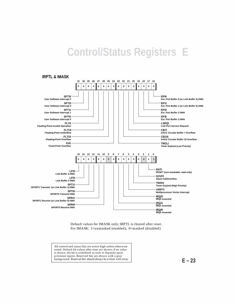
EControl/Status Registers
E – 23
All control and status bits are active high unless otherwisenoted. Default bit values after reset are shown; if no valueis shown, the bit is undefined at reset or depends uponprocessor inputs. Reserved bits are shown with a graybackground. Reserved bits should always be written with zeros.
11 10 9 8 7 6 5 4 3 2 1 015 14 13 12
0 0 0 0 0 0 0 0 0 0 0 0 0 0 1 1
SPR0ISPORT0 Receive DMA
RSTIRESET (non-maskable, read-only)
SOVFIStack Full/Overflow
TMZHITimer Expired (High Priority)
VIRPTIMultiprocessor Vector Interrupt
IRQ2IIRQ2 Asserted
IRQ1IIRQ1 Asserted
IRQ0IIRQ0 Asserted
SPR1ISPORT1 Receive (or Link Buffer 0) DMA
SPT0ISPORT0 Transmit DMA
SPT1ISPORT1 Transmit (or Link Buffer 1) DMA
LP2ILink Buffer 2 DMA
LP3ILink Buffer 3 DMA
26 25 24 23 22 21 20 19 18 1731 30 29 28 27 16
0 0 0 0 0 0 0 0 0 0 0 0 0 0 0 0
EP0IExt. Port Buffer 0 (or Link Buffer 4) DMA
LSRQILink Port Service Request
CB7IDAG1 Circular Buffer 7 Overflow
CB15IDAG2 Circular Buffer 15 Overflow
TMZLITimer Expired (Low Priority)
EP1IExt. Port Buffer 1 (or Link Buffer 5) DMA
EP2IExt. Port Buffer 2 DMA
EP3IExt. Port Buffer 3 DMA
FLTUIFloating-Point Underflow
FLTIIFloating-Point Invalid Operation
FLTOIFloating-Point Overflow
FIXIFixed-Point Overflow
SFT0IUser Software Interrupt 0
SFT1IUser Software Interrupt 1
SFT2IUser Software Interrupt 2
SFT3IUser Software Interrupt 3
Default values for IMASK only; IRPTL is cleared after reset.For IMASK: 1=unmasked (enabled), 0=masked (disabled)
IRPTL & IMASK

E Control/Status Registers
E – 24
E.9 SYSTEM CONFIGURATION (SYSCON)The SYSCON register is used to set up system configuration selections.SYSCON is memory-mapped in internal memory at address 0x0000.After reset the SYSCON register is initialized to 0x0000 0010. Thiscauses the ADSP-2106x to assume a 16-bit bus for any host processor;two 16-bit words must be written to SYSCON to change the setting ofHPM, even if the host bus is 32 bits wide.
Bit Name Definition0 SRST Software Reset1 BSO Boot Select Override2 IIVT Internal Interrupt Vector Table (for “no booting” mode)3 IWT Instruction Word Transfer (1=48-bit instruction, 0=32-bit data)4-5 HPM Host Packing Mode (00=none, 01=16-to-32, 10=16-to-48, 11=32-to-48)6 HMSWF Host Packing Order – MSW First (1=MSW first, 0=LSW first)7 HPFLSH Host Packing Status Flush8 IMDW0 Internal Memory Block 0 Data Width (0=32-bit data, 1=40-bit data)9 IMDW1 Internal Memory Block 1 Data Width (0=32-bit data, 1=40-bit data)10 ADREDY Active Drive REDY (1=active drive, 0=open drain)11 BHD Buffer Hang Disable (1=prevent hangs, 0=allow hangs)12-15 MSIZE External Memory Bank Size (MSIZE = log2(bank size) – 13)16-17 EBPR External Bus Priority (01=core processor, 10=I/O processor, 00=even)18 DCPR DMA Channel 6-9 Priority (1=rotating priority, 0=sequential priority)19-27 reserved28 IMGR Internal Memory Grouping (Mesh Multiprocessing)29-31 reserved
SRST Software Reset—Causes a software reset. This has the same effect asthe RESET pin.
BSO Boot Select Override—Deactivates the MS3-0 memory select linesand activates the BMS boot memory select output. This allows theADSP-2106x to read from its boot EPROM when it is no longer inboot mode. Since only 256 instructions can be loaded during EPROMbooting, setting the BSO bit lets the ADSP-2106x read additional codeor data from its boot EPROM after booting is completed. (See“Booting” in Chapter 11, System Design.)
1=Activate BMSBMS to read from boot EPROM
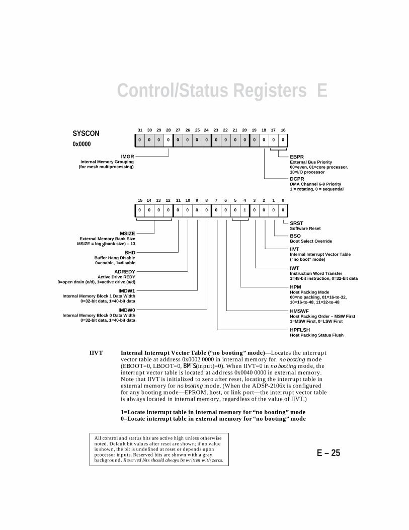
EControl/Status Registers
E – 25
11 10 9 8 7 6 5 4 3 2 1 0
000010000000
15 14 13 12
0000
26 25 24 23 22 21 20 19 18 17
000000000000
31 30 29 28 27
0000
16
SRSTSoftware Reset
BSOBoot Select Override
IIVTInternal Interrupt Vector Table(“no boot” mode)
IWTInstruction Word Transfer1=48-bit instruction, 0=32-bit data
HPMHost Packing Mode00=no packing, 01=16-to-32,10=16-to-48, 11=32-to-48
HMSWFHost Packing Order – MSW First1=MSW First, 0=LSW First
MSIZEExternal Memory Bank Size
MSIZE = log2(bank size) – 13
HPFLSHHost Packing Status Flush
IMDW1Internal Memory Block 1 Data Width
0=32-bit data, 1=40-bit data
IMDW0Internal Memory Block 0 Data Width
0=32-bit data, 1=40-bit data
EBPRExternal Bus Priority00=even, 01=core processor,10=I/O processor
DCPRDMA Channel 6-9 Priority1 = rotating, 0 = sequential
IMGRInternal Memory Grouping
(for mesh multiprocessing)
BHDBuffer Hang Disable0=enable, 1=disable
ADREDYActive Drive REDY
0=open drain (o/d), 1=active drive (a/d)
SYSCON0x0000
IIVT Internal Interrupt Vector Table (“no booting” mode)—Locates the interruptvector table at address 0x0002 0000 in internal memory for no booting mode(EBOOT=0, LBOOT=0, BMS(input)=0). When IIVT=0 in no booting mode, theinterrupt vector table is located at address 0x0040 0000 in external memory.Note that IIVT is initialized to zero after reset, locating the interrupt table inexternal memory for no booting mode. (When the ADSP-2106x is configuredfor any booting mode—EPROM, host, or link port—the interrupt vector tableis always located in internal memory, regardless of the value of IIVT.)
1=Locate interrupt table in internal memory for “no booting” mode0=Locate interrupt table in external memory for “no booting” mode
All control and status bits are active high unless otherwisenoted. Default bit values after reset are shown; if no valueis shown, the bit is undefined at reset or depends uponprocessor inputs. Reserved bits are shown with a graybackground. Reserved bits should always be written with zeros.
E Control/Status Registers
E – 26
IWT Instruction Word Transfer—Specifies the word width for direct readsand direct writes of the ADSP-2106x’s internal memory (by otherADSP-2106xs or by the host). IWT=1 overrides the IMDW bits (seebelow) and forces a 48-bit (3-column) memory transfer. IWT=0 defersto the data word setting of the IMDW bits in the SYSCON register.IWT should be set whenever the ADSP-2106x bus master or hostprocessor is reading or writing instructions from (this) ADSP-2106x.
1=48-bit words for direct read/writes0=32-bit words for direct read/writes
HPM(1:0) Host Packing Mode—Specifies the internal word width and externalhost bus width for host processor accesses of the ADSP-2106x’sinternal memory or IOP registers. If the host access is a read or writeto the external port data buffers (EPB0, EPB1, EPB2, or EPB3), theexternal host bus width selected by HPM must correspond to theexternal word width selected in the PMODE bits of the DMACxcontrol register (DMAC6, DMAC7, DMAC8, and DMAC9):
HPM and PMODE must select the same external bus widthfor host data transfers to and from the ADSP-2106x!!
If the host access is a read or write of any IOP register other than theexternal port buffers or link port buffers (LBUF0-LBUF5), the wordwidth will always be 32 bits no matter what the host bus width is. Ifthe host access is a read or write of the link port buffers, the wordwidth is determined only by HPM, and not by the LEXT bit in LCTL.
00=No packing. Maximum bus width is 32 bits for asynchronoustransfers. The lower 16 bits of the 48-bit data bus will be written andread as zeros, even when reading 48-bit words. For synchronoustransfers, the host bus should be 32 bits wide for data transfers or48 bits wide for instruction word transfers. (Note: To read and write48-bit words from internal memory, the IWT bit must be set to 1 or theIMDW bit for the block of memory being accessed must be set to 1.)
Default → 01=16-bit host bus, 32-bit words. The host bus will be 16 bits wide;at Reset any memory access will be 32-bit words.
(Note: If the memory access is made to a block of ADSP-2106x internalmemory for which the IMDW bit is set, the access will read or write theupper 32 bits of the 48-bit word.)
10=16-bit host bus, 48-bit words. The host bus will be 16 bits wide;any memory access will be 48-bit words.
11=32-bit host bus, 48-bit words. The host bus will be 32 bits wide;any memory access will be 48-bit words.
EControl/Status Registers
E – 27
To change the host packing mode, the following sequence must occur:
1. Write to the SYSCON register, changing the setting of HPM.2. Read SYSCON (and ignore data) to ensure that the write was
completed.3. Repeat the write to SYSCON (to flush the read, since it may have
occurred in the old packing mode).4. Wait 4 cycles.
HMSWF Host Packing Order – Most Significant Word First—Specifies theorder in which host-accessed words are packed, for 16-to-32 bit and16-to-48 bit packing. HMSWF is ignored for 32-to-48 bit packing.When HMSWF=1, packing is done MSW first (most significant 16-bitword first). When HMSWF=0, packing is is done LSW first.
1=MSW first0=LSW first
HPFLSH Host Packing Status Flush—Resets the host packing status. Hostaccesses must not occur while the HPFLSH bit is being written by theADSP-2106x processor core. There is a two cycle latency before thereset takes effect, after which the host may resume normal operations.(Note: HPFLSH is always read as a zero.)
1=Flush packing status
IMDWx Internal Memory Block Data Width—Selects the data word width foreach block of internal memory. For 32-bit data words, set IMDWx to 0.For 40-bit data (transferred within 48-bit words), set IMDWx to 1.IMDW0 (bit 8 of SYSCON) selects the data word width for memoryblock 0 and IMDW1 (bit 9) selects the data word width for memoryblock 1. (Note: 48-bit instructions can be stored in a memory blockregardless of the setting of the IMDWx bit. See “Configuring MemoryFor 32-Bit or 40-Bit Data” in the Memory chapter for more information.)
0=32-bit data1=40-bit data
E Control/Status Registers
E – 28
BHD Buffer Hang Disable—Disables the hang condition that occurswhen the ADSP-2106x core tries to read from an empty (or writeto a full) SPORT buffer (RX/TX), link port buffer (LBUFx), orexternal port buffer (EPBx). The hang condition also occurs whenan external device—either another ADSP-2106x or a hostprocessor—tries to read from an empty buffer or write to a fullbuffer.
After reset, BHD=0 so that buffer hang is enabled; this is thenormal mode of operation for the buffers. Setting BHD=1 todisable buffer hang is useful for debugging purposes.
(Note: The full or empty status of a particular buffer can bedetermined by reading the appropriate control/status register—DMACx for the external port buffers, LCOM for the link portbuffers, and SRCTLx/STCTLx for the SPORT buffers.)
1=prevent hangs0=allow hangs
ADREDY Active Drive REDY—Changes REDY signal to an active driveoutput.
1=active drive (a/d)0=open drain (o/d)
MSIZE(3:0) External Memory Bank Size—Selects the size of the externalmemory banks (each memory bank is the same size). The value ofMSIZE is calculated with the following equation:
MSIZE=log2(bank size) – 13
(See “External Memory Banks” in the Memory chapter for moreinformation.)
EBPR(1:0) External Bus Priority—Determines priority for use of external bus(DATA47-0 , ADDR31-0) for conflicts between the ADSP-2106x’sprocessor core and on-chip I/O processor. This type of contentionoccurs when the processor core attempts an off-chip read or writeat the same time that a DMA transfer is in progress(independently controlled by the I/O processor).
00=Even priority—both accesses alternate with each other01=Core processor has priority10=I/O processor has priority (for DMA transfer)
EControl/Status Registers
E – 29
Note: The setting of EPBR is not related to the CPA pin function(core priority access).
(Additional Details: The ADSP-2106x has three on-chip buses thatare multiplexed at the external port: the PM bus (instructions ordata), DM bus (data), and I/O bus (DMA data). The PM bus andDM bus are controlled by the ADSP-2106x processor core. TheI/O bus is controlled by the on-chip I/O processor. The I/O busconnects the external port’s DMA buffers to the ADSP-2106x’sinternal memory and IOP registers.
Contention for use of the external bus occurs when both theprocessor core and I/O processor attempt an off-chip read orwrite during the same cycle. The contention occurs at theADSP-2106x’s external port, where the three internal buses aremultiplexed together.
PM vs. DM bus conflicts are resolved with a fixed priority if theaccesses are both reads or both writes—the DM bus access occursfirst. An extra cycle is generated in the following cycle to allowthe PM bus access to occur.
For core processor priority, the I/O processor access will bedelayed until neither the PM bus nor DM bus is carrying anaccess. For I/O bus priority, the PM and/or DM bus accesseswill be delayed until all pending I/O bus accesses are completed.)
Note: For even priority, if both the core and I/O processor try touse the external bus continuously, they will each get a bus slotevery other cycle.
DCPR DMA Channel 6-9 Priority—Selects rotating or sequential priorityfor DMA channels 6-9. When DCPR is set to 1, a rotating priorityscheme is implemented in which priority moves to the nexthighest numbered channel (modulo 4). When DCPR is 0, highestpriority is assigned to channel 6 and lowest priority to channel 9.
1=Rotating priority0=Sequential priority (ch6 high – ch9 low)
E.10 SYSTEM STATUS (SYSTAT)The SYSTAT register provides status information, primarily formultiprocessor systems. SYSTAT is memory-mapped in internal
E Control/Status Registers
E – 30
memory at address 0x0003. After reset, all bits in SYSTAT are initializedto zero except for IDC(2:0) and CRBM(2:0). IDC(2:0) will be equal to thevalue of the ADSP-2106x’s ID2-0 inputs. CRBM(2:0) is equal to the ID ofthe current bus master, for ID>0. For ID=0, CRBM=1.
Bit Name Definition0 HSTM Host Mastership1 BSYN Bus Synchronization2-3 reserved4-6 CRBM Current Bus Master (ID2-0 of ADSP-2106x bus master)7 reserved8-10 IDC ID Code (ID2-0 of this ADSP-2106x)11 reserved12 DWPD Direct Write Pending13 VIPD Vector Interrupt Pending14-15 HPS Host Packing Status16-31 reserved
HSTM Host Mastership—Indicates whether the host processor has beengranted control of the bus.
1=Host is bus master0=Host is not bus master
BSYN Bus Synchronization—Indicates when the ADSP-2106x’s busarbitration logic is synchronized after reset. (See “BusSynchronization After Reset” in the Multiprocessing chapter of thismanual for details.)
1=Bus arbitration logic is synchronized0=Bus arbitration logic is not synchronized
CRBM(2:0) Current Bus Master—Indicates the ID of the ADSP-2106x that is thecurrent bus master. If CRBM is equal to the ID of this ADSP-2106xthen it is the current bus master. CRBM is only valid for ID2-0 > 0(greater than zero). When ID2-0=000, CRBM is always 1.
IDC(2:0) ID Code—Indicates the ID2-0 inputs of this ADSP-2106x.
DWPD Direct Write Pending—Indicates when a direct write to theADSP-2106x’s internal memory is pending. The DWPD bit is clearedwhen the direct write has been completed. (Direct writes may bedelayed for several cycles if DMA chaining is underway or if higher

EControl/Status Registers
E – 31
SYSTAT0x0003
11 10 9 8 7 6 5 4 3 2 1 0
00000000
15 14 13 12
0000
26 25 24 23 22 21 20 19 18 17
000000000000
31 30 29 28 27
0000
16
HSTMHost Mastership
CRBMCurrent Bus Master
DWPDDirect Write Pending
HPSHost Packing Status00 = packing complete01 = first stage of all packing and unpacking modes10 = second stage of 16-to-48 bit packing/unpacking or 32-to-48 bit packing/unpacking
BSYNBus Synchronization
IDCID Code
VIPDVector Interrupt Pending
All control and status bits are active high unless otherwisenoted. Default bit values after reset are shown; if no valueis shown, the bit is undefined at reset or depends uponprocessor inputs. Reserved bits are shown with a graybackground. Reserved bits should always be written with zeros.
priority DMA requests occur. Maximum delay is 12 cycles.)
1=Direct write pending0=No direct write pending
VIPD Vector Interrupt Pending—Indicates that a pending vector interrupt hasnot yet been serviced. The VIPD bit is set when the VIRPT register iswritten to and is cleared upon return from the interrupt service routine.The host processor (or other ADSP-2106x) that issued the vector interruptshould monitor this bit to determine when the service routine has beencompleted (and when a new vector interrupt may be issued).
1=Vector interrupt pending0=No vector interrupt pending
HPS(1:0) Host Packing Status—Indicates when host word packing is completedor, if not, what stage of the process is taking place.
00=Packing complete
E Control/Status Registers
E – 32
01=First stage of all packing and unpacking modes.10=Second stage of 16-to-48 bit packing/unpacking or 32-to-48 bitpacking/unpacking
E.11 EXTERNAL MEMORY WAIT STATE CONTROL (WAIT)The WAIT register is used to set up external memory wait states andresponse to the ACK signal. WAIT is memory-mapped in internalmemory at address 0x0002. The WAIT register is initialized to0x21AD 6B5A after a processor reset; this configures the ADSP-2106xfor 1) no idle state on PAGE boundary crossings, 2) six internal waitstates, 3) dependence on ACK for all memory banks and for unbankedmemory, and 4) multiprocessor memory space wait state enabled.
Bit Name Definition0-1 EB0WM External Bank 0 wait state mode2-4 EB0WS External Bank 0 number of wait states5-6 EB1WM External Bank 1 wait state mode7-9 EB1WS External Bank 1 number of wait states10-11 EB2WM External Bank 2 wait state mode12-14 EB2WS External Bank 2 number of wait states15-16 EB3WM External Bank 3 wait state mode17-19 EB3WS External Bank 3 number of wait states20-21 UBWM Unbanked memory wait state mode*22-24 UBWS Unbanked memory number of wait states*25-27 PAGSZ Page size for DRAM (only in Bank 0)28 PAGEIS Single idle cycle on DRAM page boundary crossing29 MMSWS Single wait state for Multiprocessor Memory Space access30 HIDMA Single idle cycle for DMA handshake31 reserved* Unbanked memory wait states and wait state mode are applied to BMS-asserted
accesses.
Wait State Mode
EBxWM Wait State Mode00 External acknowledge only (ACK)01 Internal wait states only10 Both internal and external acknowledge required11 Either internal or external acknowledge sufficient
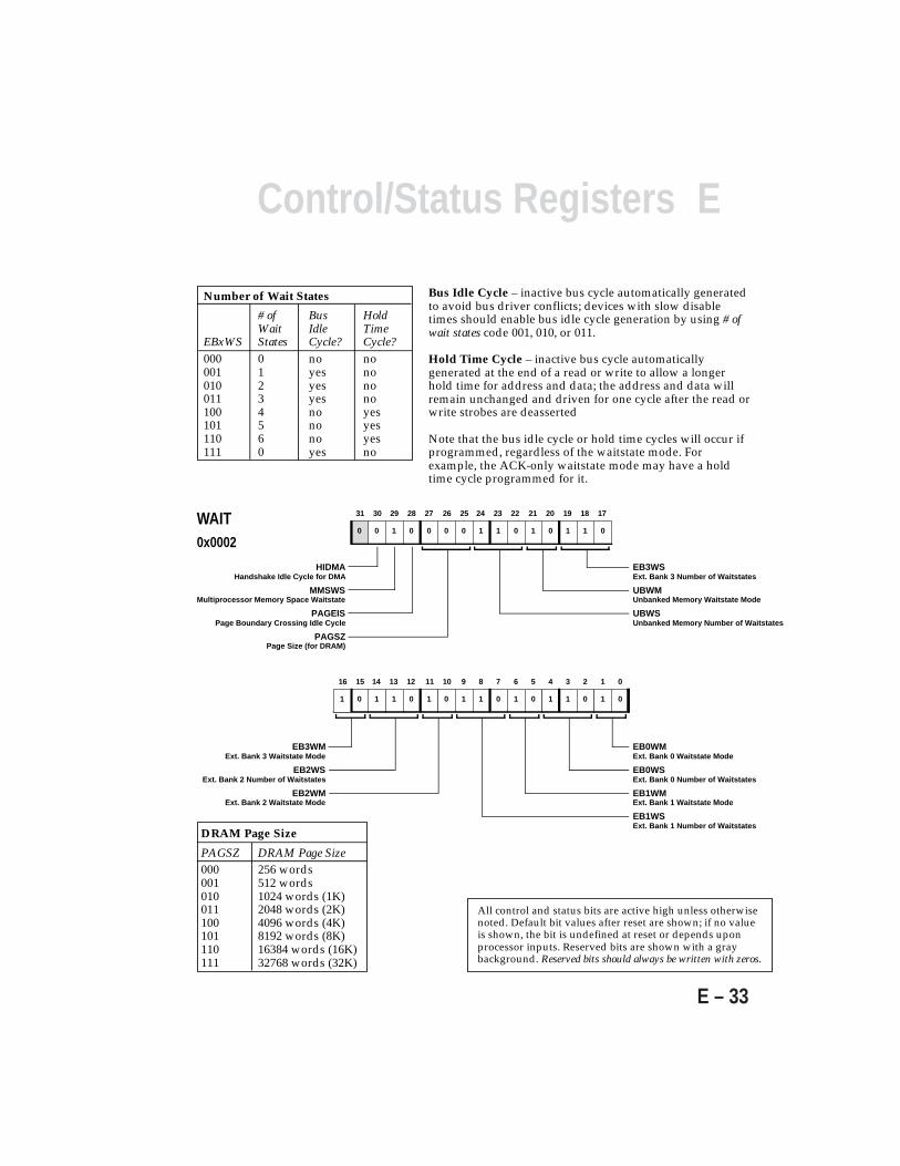
EControl/Status Registers
E – 33
All control and status bits are active high unless otherwisenoted. Default bit values after reset are shown; if no valueis shown, the bit is undefined at reset or depends uponprocessor inputs. Reserved bits are shown with a graybackground. Reserved bits should always be written with zeros.
DRAM Page Size
PAGSZ DRAM Page Size000 256 words001 512 words010 1024 words (1K)011 2048 words (2K)100 4096 words (4K)101 8192 words (8K)110 16384 words (16K)111 32768 words (32K)
Number of Wait States
# of Bus HoldWait Idle Time
EBxWS States Cycle? Cycle?000 0 no no001 1 yes no010 2 yes no011 3 yes no100 4 no yes101 5 no yes110 6 no yes111 0 yes no
Bus Idle Cycle – inactive bus cycle automatically generatedto avoid bus driver conflicts; devices with slow disabletimes should enable bus idle cycle generation by using # ofwait states code 001, 010, or 011.
Hold Time Cycle – inactive bus cycle automaticallygenerated at the end of a read or write to allow a longerhold time for address and data; the address and data willremain unchanged and driven for one cycle after the read orwrite strobes are deasserted
Note that the bus idle cycle or hold time cycles will occur ifprogrammed, regardless of the waitstate mode. Forexample, the ACK-only waitstate mode may have a holdtime cycle programmed for it.
11 10 9 8 7 6 5 4 3 2 1 0
010110101101
15 14 13 12
0110
EB0WMExt. Bank 0 Waitstate Mode
EB0WSExt. Bank 0 Number of Waitstates
EB1WMExt. Bank 1 Waitstate Mode
EB1WSExt. Bank 1 Number of Waitstates
16
EB3WMExt. Bank 3 Waitstate Mode
EB2WSExt. Bank 2 Number of Waitstates
EB2WMExt. Bank 2 Waitstate Mode
26 25 24 23 22 21 20 19 18 17
01101011000
31 30 29 28 27
0100
EB3WSExt. Bank 3 Number of Waitstates
UBWMUnbanked Memory Waitstate Mode
UBWSUnbanked Memory Number of Waitstates
HIDMAHandshake Idle Cycle for DMA
MMSWSMultiprocessor Memory Space Waitstate
PAGEIS Page Boundary Crossing Idle Cycle
PAGSZ Page Size (for DRAM)
1
WAIT0x0002
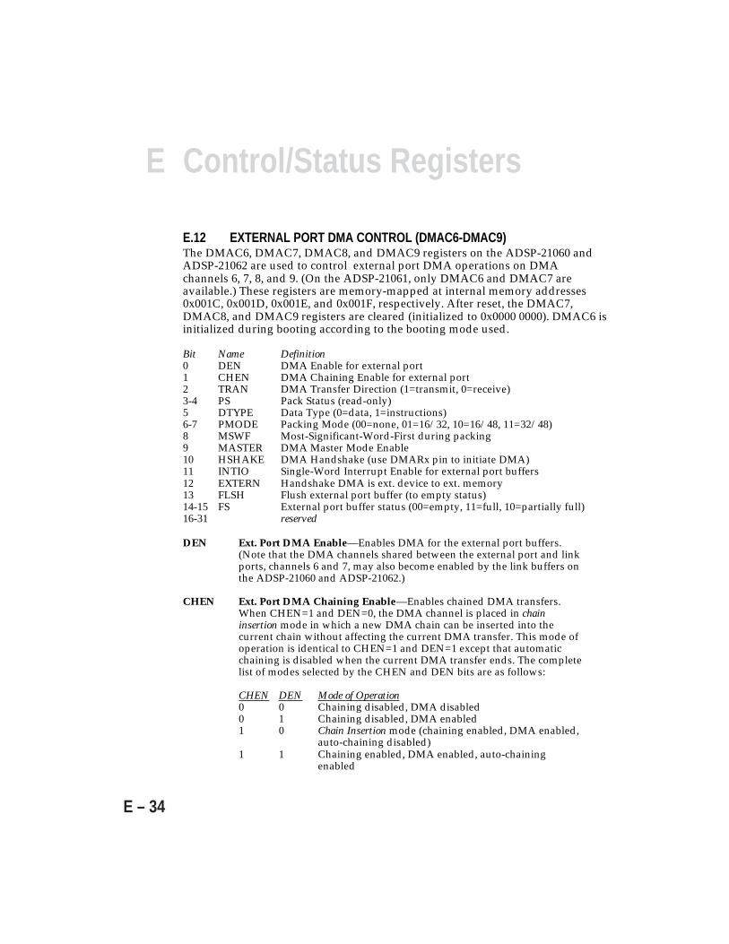
E Control/Status Registers
E – 34
E.12 EXTERNAL PORT DMA CONTROL (DMAC6-DMAC9)The DMAC6, DMAC7, DMAC8, and DMAC9 registers on the ADSP-21060 andADSP-21062 are used to control external port DMA operations on DMAchannels 6, 7, 8, and 9. (On the ADSP-21061, only DMAC6 and DMAC7 areavailable.) These registers are memory-mapped at internal memory addresses0x001C, 0x001D, 0x001E, and 0x001F, respectively. After reset, the DMAC7,DMAC8, and DMAC9 registers are cleared (initialized to 0x0000 0000). DMAC6 isinitialized during booting according to the booting mode used.
Bit Name Definition0 DEN DMA Enable for external port1 CHEN DMA Chaining Enable for external port2 TRAN DMA Transfer Direction (1=transmit, 0=receive)3-4 PS Pack Status (read-only)5 DTYPE Data Type (0=data, 1=instructions)6-7 PMODE Packing Mode (00=none, 01=16/32, 10=16/48, 11=32/48)8 MSWF Most-Significant-Word-First during packing9 MASTER DMA Master Mode Enable10 HSHAKE DMA Handshake (use DMARx pin to initiate DMA)11 INTIO Single-Word Interrupt Enable for external port buffers12 EXTERN Handshake DMA is ext. device to ext. memory13 FLSH Flush external port buffer (to empty status)14-15 FS External port buffer status (00=empty, 11=full, 10=partially full)16-31 reserved
DEN Ext. Port DMA Enable—Enables DMA for the external port buffers.(Note that the DMA channels shared between the external port and linkports, channels 6 and 7, may also become enabled by the link buffers onthe ADSP-21060 and ADSP-21062.)
CHEN Ext. Port DMA Chaining Enable—Enables chained DMA transfers.When CHEN=1 and DEN=0, the DMA channel is placed in chaininsertion mode in which a new DMA chain can be inserted into thecurrent chain without affecting the current DMA transfer. This mode ofoperation is identical to CHEN=1 and DEN=1 except that automaticchaining is disabled when the current DMA transfer ends. The completelist of modes selected by the CHEN and DEN bits are as follows:
CHEN DEN Mode of Operation0 0 Chaining disabled, DMA disabled0 1 Chaining disabled, DMA enabled1 0 Chain Insertion mode (chaining enabled, DMA enabled,
auto-chaining disabled)1 1 Chaining enabled, DMA enabled, auto-chaining
enabled
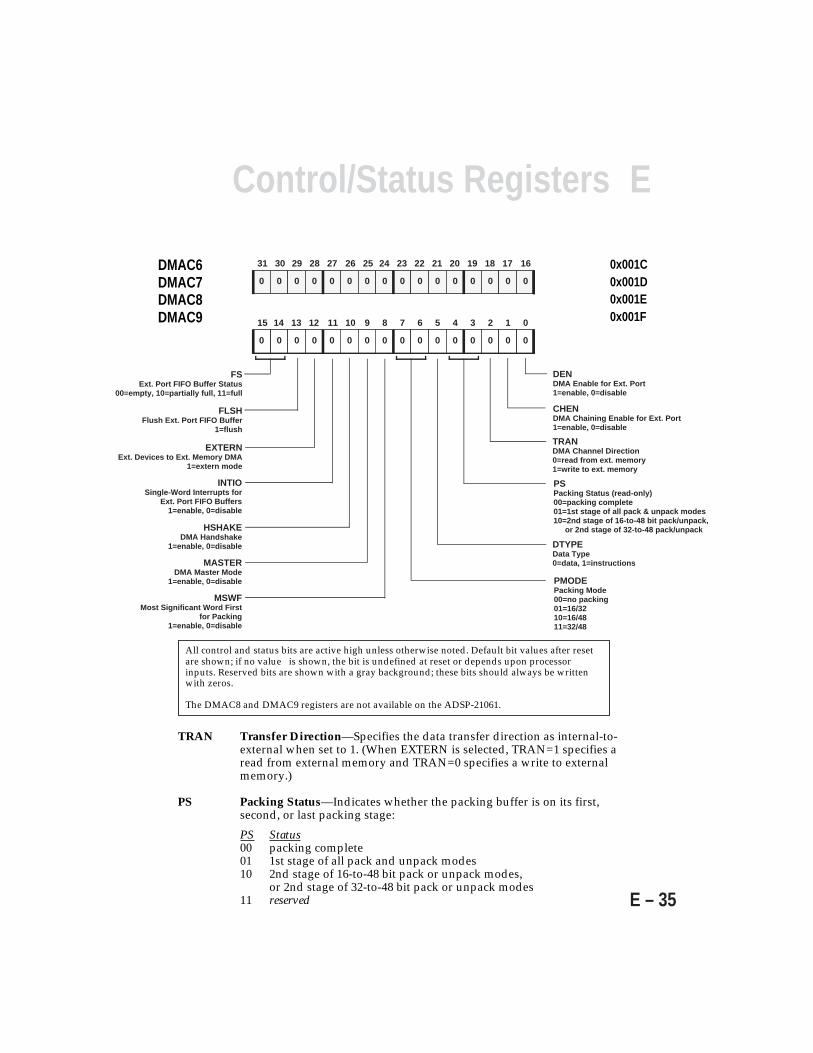
EControl/Status Registers
E – 35
0x001C0x001D0x001E0x001F11 10 9 8 7 6 5 4 3 2 1 0
000000000000
15 14 13 12
0000
DENDMA Enable for Ext. Port1=enable, 0=disable
CHENDMA Chaining Enable for Ext. Port1=enable, 0=disable
TRANDMA Channel Direction0=read from ext. memory1=write to ext. memory
PSPacking Status (read-only)00=packing complete01=1st stage of all pack & unpack modes10=2nd stage of 16-to-48 bit pack/unpack,
or 2nd stage of 32-to-48 pack/unpack
FLSHFlush Ext. Port FIFO Buffer
1=flush
EXTERNExt. Devices to Ext. Memory DMA
1=extern mode
FSExt. Port FIFO Buffer Status
00=empty, 10=partially full, 11=full
AA26AA25AA24AA23AA22 A21 A20AA19AA18AA17
000000000000AA31AA30AA29AA28 A27
0000AA16
DTYPEData Type0=data, 1=instructions
PMODEPacking Mode00=no packing01=16/3210=16/4811=32/48
INTIOSingle-Word Interrupts for
Ext. Port FIFO Buffers1=enable, 0=disable
HSHAKEDMA Handshake
1=enable, 0=disable
MASTERDMA Master Mode
1=enable, 0=disable
MSWFMost Significant Word First
for Packing1=enable, 0=disable
DMAC6DMAC7DMAC8DMAC9
All control and status bits are active high unless otherwise noted. Default bit values after resetare shown; if no value is shown, the bit is undefined at reset or depends upon processorinputs. Reserved bits are shown with a gray background; these bits should always be writtenwith zeros.
The DMAC8 and DMAC9 registers are not available on the ADSP-21061.
TRAN Transfer Direction—Specifies the data transfer direction as internal-to-external when set to 1. (When EXTERN is selected, TRAN=1 specifies aread from external memory and TRAN=0 specifies a write to externalmemory.)
PS Packing Status—Indicates whether the packing buffer is on its first,second, or last packing stage:
PS Status00 packing complete01 1st stage of all pack and unpack modes10 2nd stage of 16-to-48 bit pack or unpack modes,
or 2nd stage of 32-to-48 bit pack or unpack modes11 reserved

E Control/Status Registers
E – 36
DTYPE Data Type—Specifies the type of data being transferred; thisinformation is used by internal memory to determine the wordwidth. DTYPE=1 overrides the IMDW bits and forces a 48-bit (3-column) memory transfer. DTYPE=0 defers to the data word settingof the IMDW bits in the SYSCON register. The data word may be 32-bit or 40-bit, as determined by the setting of the IMDW bits in theSYSCON register.
PMODE Packing Mode—Specifies the EPBx buffer packing mode. For hostprocessor accesses of the EPBx buffers, the HPM bits of the SYSCONregister must be set to correspond to the external bus width specifiedby PMODE.
PMODE Packing Mode00 No packing/unpacking01 16-bit external bus to/from 32-bit internal packing10 16-bit external bus to/from 48-bit internal packing11 32-bit external bus to/from 48-bit internal packing
MSWF Most Significant Word First—Specifies the order in which words arepacked, for 16-to-32 bit packing and 16-to-48 bit packing. MSWF isignored for 32-to-48 bit packing. When MSWF=1, packing is doneMSW first (most significant 16-bit word first). When MSWF=0,packing is is done LSW first.
1=MSW first0=LSW first
INTIO Single-Word I/O Interrupts—Used when DEN=0, to allow theexternal port DMA interrupts to occur for individual words receivedand transmitted. Generating DMA interrupts in this fashion is usefulfor implementing interrupt-driven single-word transfers undercontrol of the ADSP-2106x core processor. Setting INTIO=1 causesthe interrupts to occur when an EPBx input buffer is “not empty” (forTRAN=0) or when an output buffer is “not full” (for TRAN=1).
FLSH Flush DMA Channel—Reinitializes the state of the DMA channel,clearing the FS and PS status bits to zero. The EPBx buffer is flushed,and any internal DMA states are reset. This operation has a two-cyclelatency. FLSH is a self-clearing control bit which is not latched andwill always read as a 0.
The FLSH bit should only be used to clear the DMA channel whenthe channel is not active. Use of the FLSH bit while the channel is activemay cause unexpected results. The DMASTAT register can be read todetermine if the channel is active. (For a particular channel, thechannel active status bit in DMASTAT will be set if DMA is enabledand the current DMA sequence has not completed.) Also, due to the
EControl/Status Registers
E – 37
added latency of the FLSH bit, it should not be set in the sameDMACx write in which the DEN bit is set. As a general rule, setFLSH at least one cycle before setting any other DMACx control bits.
FS EPBx Buffer Status—FS is a two-bit status field that indicateswhether data is present in the EPBx buffer. When data is beingtransferred out from the ADSP-2106x, these status bits indicatewhether there is room in the buffer for more data.When data is being transferred into the ADSP-2106x, these status bitsindicate whether new (unread) data is available in the buffer.
FS Status00 empty01 undefined10 partially full11 full
MASTER Master Mode DMA Enable—The MASTER, HSHAKE, and EXTERNbits are used in combination, as described below.
HSHAKE Handshake DMA Enable—The MASTER, HSHAKE, and EXTERNbits are used in combination, as described below.
EXTERN External Handshake Mode Enable—Specifies an external memory toexternal device DMA transfer. HSHAKE must equal 1 and MASTERequal 0 in this mode.
E Control/Status Registers
E – 38
The MASTER, HSHAKE, and EXTERN bits are used in combination toprovide the following DMA transfer modes:
M H E DMA Mode of Operation1
0 0 0 Slave Mode. The DMA request is generated whenever the receivebuffer is not empty or the transmit buffer is not full.2
0 0 1 Reserved0 1 0 Handshake Mode. (For the ADSP-21060 and ADSP-21062,
applies to EPB1, EPB2 buffers, channels 7, 8 only. For the ADSP-21061, applies to EPB0, EPB1 buffers, channels 6, 7 only.) TheDMA request is generated when the DMARx line is asserted. Thetransfer occurs when DMAGx is asserted.1
0 1 1 External Handshake Mode. (For the ADSP-21060 and ADSP-21062, applies to EPB1, EPB2 buffers, channels 7, 8 only. For theADSP-21061, applies to EPB0, EPB1 buffers, channels 6, 7 only.)Identical to Handshake Mode, but with data transferred betweenexternal memory and an external device.
1 0 0 Master Mode. The DMA controller will attempt a transferwhenever the receive buffer is not empty or the transmit buffer isnot full and the DMA counter is non-zero.1 DMAR1 should bekept high (inactive) if channel 7 is in master mode, and DMAR2should be kept high if channel 8 is in master mode on the ADSP-21060 or ADSP-21062. DMAR2 should be kept high if channel 6 isin master mode on the ADSP-21061.
1 0 1 Reserved1 1 0 Paced Master Mode. (For the ADSP-21060 and ADSP-21062,
applies to EPB1, EPB2 buffers, channels 7, 8 only. For the ADSP-21061, applies to EPB0, EPB1 buffers, channels 6, 7 only.) In thismode the transfers are paced by the DMARx signal—the DMArequest is generated when DMARx is asserted. DMARx requestsoperate in the same way as in handshake mode. The bus transferoccurs when RD or WR is asserted. The address is driven as innormal master mode. No external gates are required to OR theRD-DMAGx and WR-DMAGx pairs, thus allowing the bufferaccess to be zero-waitstate with no idle states. Waitstates andacknowledge (ACK) apply to Paced Master Mode transfers; seeSection 5.4.4, “Wait States & Acknowledge” in Chapter 5,Memory.
1 1 1 Reserved
1. When an external port DMA channel is configured for output (i.e.,TRAN=1), the EPBx buffer will start to fill as soon as that DMA channel isenabled. The EPBx buffer will start to fill up even if no DMAR assertions orslave mode DMA buffer reads have been made yet.
2. If data is to be read from the ADSP-2106x (i.e. TRAN=1), the EPBx bufferwill be filled as soon as the DEN enable bit is set to 1.

EControl/Status Registers
E – 39
E.13 DMA CHANNEL STATUS (DMASTAT)The DMASTAT register maintains status bits for each DMA channel. Thisregister is memory-mapped at internal memory addresses 0x0037. For aparticular channel, the channel active status bit will be set if DMA isenabled and the current DMA sequence has not completed. The chainingstatus bit will be set if the channel is currently performing chainingoperations or if chaining is pending. There is a single cycle of latencybetween internal status changes and the update of the DMASTAT register.
Bit Definition0 DMA Channel 0 Status1
1 DMA Channel 1 Status1
2 DMA Channel 2 Status1
3 DMA Channel 3 Status1
4 DMA Channel 4 Status1, 2
5 DMA Channel 5 Status1, 2
6 DMA Channel 6 Status1
7 DMA Channel 7 Status1
8 DMA Channel 8 Status1
9 DMA Channel 9 Status1
10 DMA Channel 0 Chaining Status3
11 DMA Channel 1 Chaining Status3
12 DMA Channel 2 Chaining Status3
13 DMA Channel 3 Chaining Status3
14 DMA Channel 4 Chaining Status2, 3
15 DMA Channel 5 Chaining Status2, 3
16 DMA Channel 6 Chaining Status3
17 DMA Channel 7 Chaining Status3
18 DMA Channel 8 Chaining Status3
19 DMA Channel 9 Chaining Status3
20-31 undefined/reserved
1. Channel Status: 1 (active)=transferring data or waiting to transfer the currentblock, and not transferring TCB. 0 (inactive)=DMA disabled, transfer complete, orchaining.
2. Not valid for the ADSP-21061.3. Channel Chaining Status: 1=transferring TCB or waiting to transfer TCB.
0=chaining disabled.
Note 1: Status does not change on the master ADSP-2106x during external port DMAuntil the external portion is completed (i.e., the EPBx buffers are emptied).
Note 2: If in chain insertion mode (DEN=0, CHEN=1), then channel chaining statuswill never go to 1. Therefore, test channel status to see if it is ready so thatyour program can rewrite the chain pointer (CPx register).
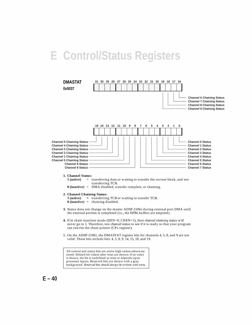
E Control/Status Registers
E – 40
27 26 25 24 23 22 21 20 19 18 17 1631 30 29 28
AAAAAAAAAAAAAAAA
11 10 9 8 7 6 5 4 3 2 1 015 14 13 12
Channel 0 Status
AAAAAAAAAAAAAAAA
Channel 1 StatusChannel 2 StatusChannel 3 StatusChannel 4 StatusChannel 5 StatusChannel 6 StatusChannel 7 Status
Channel 4 Chaining Status
Channel 9 StatusChannel 8 Status
Channel 3 Chaining StatusChannel 2 Chaining StatusChannel 1 Chaining StatusChannel 0 Chaining Status
Channel 5 Chaining Status
Channel 6 Chaining StatusChannel 7 Chaining StatusChannel 8 Chaining StatusChannel 9 Chaining Status
DMASTAT0x0037
1. Channel Status:1 (active) = transferring data or waiting to transfer the current block, and not
transferring TCB.0 (inactive) = DMA disabled, transfer complete, or chaining.
2. Channel Chaining Status:1 (active) = transferring TCB or waiting to transfer TCB.0 (inactive) = chaining disabled.
3. Status does not change on the master ADSP-2106x during external port DMA untilthe external portion is completed (i.e., the EPBx buffers are emptied).
4. If in chain insertion mode (DEN=0, CHEN=1), then channel chaining status willnever go to 1. Therefore, test channel status to see if it is ready so that your programcan rewrite the chain pointer (CPx register).
5. On the ADSP-21061, the DMASTAT register bits for channels 4, 5, 8, and 9 are notvalid. These bits include bits: 4, 5, 8, 9, 14, 15, 18, and 19.
All control and status bits are active high unless otherwisenoted. Default bit values after reset are shown; if no valueis shown, the bit is undefined at reset or depends uponprocessor inputs. Reserved bits are shown with a graybackground. Reserved bits should always be written with zeros.
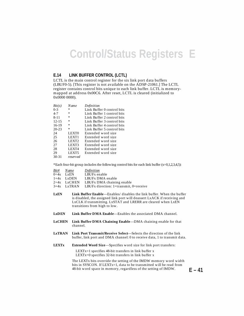
EControl/Status Registers
E – 41
E.14 LINK BUFFER CONTROL (LCTL)LCTL is the main control register for the six link port data buffers(LBUF0-5). [This register is not available on the ADSP-21061.] The LCTLregister contains control bits unique to each link buffer. LCTL is memory-mapped at address 0x00C6. After reset, LCTL is cleared (initialized to0x0000 0000).
Bit(s) Name Definition0-3 * Link Buffer 0 control bits4-7 * Link Buffer 1 control bits8-11 * Link Buffer 2 control bits12-15 * Link Buffer 3 control bits16-19 * Link Buffer 4 control bits20-23 * Link Buffer 5 control bits24 LEXT0 Extended word size25 LEXT1 Extended word size26 LEXT2 Extended word size27 LEXT3 Extended word size28 LEXT4 Extended word size29 LEXT5 Extended word size30-31 reserved
* Each four-bit group includes the following control bits for each link buffer (x=0,1,2,3,4,5):
Bit# Name Definition0+4x LxEN LBUFx enable1+4x LxDEN LBUFx DMA enable2+4x LxCHEN LBUFx DMA chaining enable3+4x LxTRAN LBUFx direction: 1=transmit, 0=receive
LxEN Link Buffer Enable—Enables/disables the link buffer. When the bufferis disabled, the assigned link port will deassert LxACK if receiving andLxCLK if transmitting. LxSTAT and LRERR are cleared when LxENtransitions from high to low.
LxDEN Link Buffer DMA Enable—Enables the associated DMA channel.
LxCHEN Link Buffer DMA Chaining Enable—DMA chaining enable for thatchannel.
LxTRAN Link Port Transmit/Receive Select—Selects the direction of the linkbuffer, link port and DMA channel: 0 to receive data, 1 to transmit data.
LEXTx Extended Word Size—Specifies word size for link port transfers:
LEXTx=1 specifies 48-bit transfers in link buffer x LEXTx=0 specifies 32-bit transfers in link buffer x
The LEXTx bits override the setting of the IMDW memory word widthbits in SYSCON. If LEXTx=1, data to be transmitted will be read from48-bit word space in memory, regardless of the setting of IMDW.
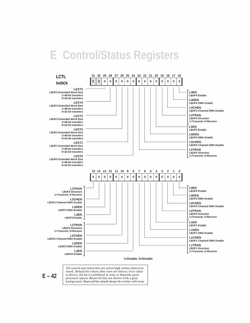
E Control/Status Registers
E – 42
11 10 9 8 7 6 5 4 3 2 1 0
000000000000
15 14 13 12
0000
L0ENLBUF0 Enable
1=Enable, 0=Disable
L0DENLBUF0 DMA Enable
L0CHENLBUF0 Chained DMA Enable
L0TRANLBUF0 Direction1=Transmit, 0=Receive
L1ENLBUF1 Enable
L1DENLBUF1 DMA Enable
L1CHENLBUF1 Chained DMA Enable
L1TRANLBUF1 Direction1=Transmit, 0=Receive
L3ENLBUF3 Enable
L3DENLBUF3 DMA Enable
L3CHENLBUF3 Chained DMA Enable
L3TRANLBUF3 Direction
1=Transmit, 0=Receive
L2ENLBUF2 Enable
L2DENLBUF2 DMA Enable
L2CHENLBUF2 Chained DMA Enable
L2TRANLBUF2 Direction
1=Transmit, 0=Receive
27 26 25 24 23 22 21 20 19 18 17 16
000000000000
31 30 29 28
0000
L4ENLBUF4 Enable
L4DENLBUF4 DMA Enable
L4CHENLBUF4 Chained DMA Enable
L4TRANLBUF4 Direction1=Transmit, 0=Receive
L5ENLBUF5 Enable
L5DENLBUF5 DMA Enable
L5CHENLBUF5 Chained DMA Enable
L5TRANLBUF5 Direction1=Transmit, 0=ReceiveLEXT0
LBUF0 Extended Word Size1=48-bit transfers0=32-bit transfers
LEXT1LBUF1 Extended Word Size
1=48-bit transfers0=32-bit transfers
LEXT2LBUF2 Extended Word Size
1=48-bit transfers0=32-bit transfers
LEXT3LBUF3 Extended Word Size
1=48-bit transfers0=32-bit transfers
LEXT4LBUF4 Extended Word Size
1=48-bit transfers0=32-bit transfers
LEXT5LBUF5 Extended Word Size
1=48-bit transfers0=32-bit transfers
All control and status bits are active high unless otherwisenoted. Default bit values after reset are shown; if no valueis shown, the bit is undefined at reset or depends uponprocessor inputs. Reserved bits are shown with a graybackground. Reserved bits should always be written with zeros.
LCTL0x00C6
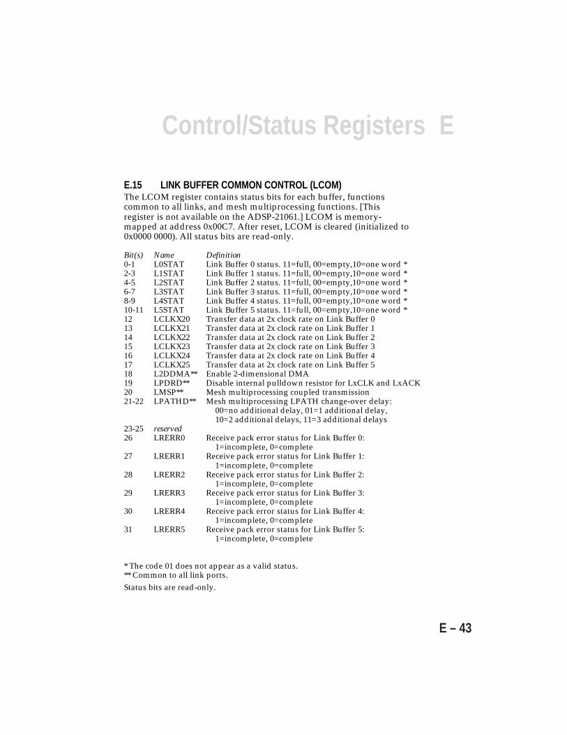
EControl/Status Registers
E – 43
E.15 LINK BUFFER COMMON CONTROL (LCOM)The LCOM register contains status bits for each buffer, functionscommon to all links, and mesh multiprocessing functions. [Thisregister is not available on the ADSP-21061.] LCOM is memory-mapped at address 0x00C7. After reset, LCOM is cleared (initialized to0x0000 0000). All status bits are read-only.
Bit(s) Name Definition0-1 L0STAT Link Buffer 0 status. 11=full, 00=empty,10=one word *2-3 L1STAT Link Buffer 1 status. 11=full, 00=empty,10=one word *4-5 L2STAT Link Buffer 2 status. 11=full, 00=empty,10=one word *6-7 L3STAT Link Buffer 3 status. 11=full, 00=empty,10=one word *8-9 L4STAT Link Buffer 4 status. 11=full, 00=empty,10=one word *10-11 L5STAT Link Buffer 5 status. 11=full, 00=empty,10=one word *12 LCLKX20 Transfer data at 2x clock rate on Link Buffer 013 LCLKX21 Transfer data at 2x clock rate on Link Buffer 114 LCLKX22 Transfer data at 2x clock rate on Link Buffer 215 LCLKX23 Transfer data at 2x clock rate on Link Buffer 316 LCLKX24 Transfer data at 2x clock rate on Link Buffer 417 LCLKX25 Transfer data at 2x clock rate on Link Buffer 518 L2DDMA** Enable 2-dimensional DMA19 LPDRD** Disable internal pulldown resistor for LxCLK and LxACK20 LMSP** Mesh multiprocessing coupled transmission21-22 LPATHD** Mesh multiprocessing LPATH change-over delay:
00=no additional delay, 01=1 additional delay,10=2 additional delays, 11=3 additional delays
23-25 reserved26 LRERR0 Receive pack error status for Link Buffer 0:
1=incomplete, 0=complete27 LRERR1 Receive pack error status for Link Buffer 1:
1=incomplete, 0=complete28 LRERR2 Receive pack error status for Link Buffer 2:
1=incomplete, 0=complete29 LRERR3 Receive pack error status for Link Buffer 3:
1=incomplete, 0=complete30 LRERR4 Receive pack error status for Link Buffer 4:
1=incomplete, 0=complete31 LRERR5 Receive pack error status for Link Buffer 5:
1=incomplete, 0=complete
* The code 01 does not appear as a valid status.** Common to all link ports.Status bits are read-only.
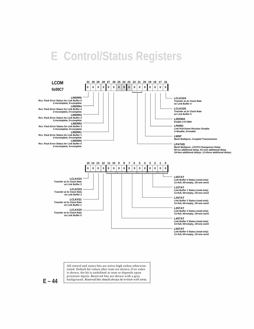
E Control/Status Registers
E – 44
All control and status bits are active high unless otherwisenoted. Default bit values after reset are shown; if no valueis shown, the bit is undefined at reset or depends uponprocessor inputs. Reserved bits are shown with a graybackground. Reserved bits should always be written with zeros.
11 10 9 8 7 6 5 4 3 2 1 0
000000000000
15 14 13 12
0000
26 25 24 23 22 21 20 19 18 17
000000000000
31 30 29 28 27
0000
16
L0STATLink Buffer 0 Status (read-only)11=full, 00=empty, 10=one word
L1STATLink Buffer 1 Status (read-only)11=full, 00=empty, 10=one word
L2STATLink Buffer 2 Status (read-only)11=full, 00=empty, 10=one word
L3STATLink Buffer 3 Status (read-only)11=full, 00=empty, 10=one word
L4STATLink Buffer 4 Status (read-only)11=full, 00=empty, 10=one word
L5STATLink Buffer 5 Status (read-only)11=full, 00=empty, 10=one word
LCLKX23Transfer at 2x Clock Rate
on Link Buffer 3
LCLKX22Transfer at 2x Clock Rate
on Link Buffer 2
LCLKX21Transfer at 2x Clock Rate
on Link Buffer 1
LCLKX20Transfer at 2x Clock Rate
on Link Buffer 0
LPATHDMesh Multiproc. LPATH Changeover Delay00=no additional delay, 01=one additional delay10=two additional delays, 11=three additional delays
LCLKX24Transfer at 2x Clock Rate on Link Buffer 4
LCLKX25Transfer at 2x Clock Rate on Link Buffer 5
L2DDMAEnable 2-D DMA
LPDRDLink Pull-Down Resistor Disable1=disable, 0=enable
LMSPMesh Multiproc.-Coupled Transmission
LRERR5Rcv. Pack Error Status for Link Buffer 5
1=incomplete, 0=completeLRERR4
Rcv. Pack Error Status for Link Buffer 41=incomplete, 0=complete
LRERR3Rcv. Pack Error Status for Link Buffer 3
1=incomplete, 0=completeLRERR2
Rcv. Pack Error Status for Link Buffer 21=incomplete, 0=complete
LRERR1Rcv. Pack Error Status for Link Buffer 1
1=incomplete, 0=completeLRERR0
Rcv. Pack Error Status for Link Buffer 01=incomplete, 0=complete
LCOM0x00C7

EControl/Status Registers
E – 45
LxSTAT(0:1) Link Buffer Status—When transmitting, these status bitsindicate whether there is room in the buffer for more data. Whenreceiving, these status bits indicate whether new (unread) data isavailable in the receive buffer. LxSTAT(1)=1 if there is data inthe buffer. LxSTAT(0)=0 if there is room in the buffer. These bitsare cleared when LxEN changes from 1 to 0. They maysubsequently change state when the data buffer is read orwritten.
LCLKX2x 2x Clock Rate—This specifies link transfers to operate at twicethe ADSP-2106x clock rate. If LCLKX2x=0, transmit transfersoccur at the ADSP-2106x clock frequency, and receive transfersoccur at (up to) the ADSP-2106x clock frequency. Set LCLKX2x=1for receive transfers occurring at greater than the ADSP-2106xclock frequency.
L2DDMA 2-D DMA Enable—This directs the DMA controller to addressmemory as a two-dimensional array as specified in the DMAaddress registers. Only DMA channels 0-5 support 2D DMA.Link ports 4 and 5 on DMA channels 6 and 7 do not have 2DDMA support.
LPDRD Disable Pulldown Resistors—This disables the internal 50 kΩpulldown resistors on the LxACK, LxCLK, and LxDAT3-0 pinsfor disabled link ports. When this bit is clear, the pulldownresistors are enabled.
LMSP Mesh Multiprocessing Enable—Enables link port meshmultiprocessing. In non-mesh-multiprocessing operation(LMSP=0), all six link buffers operate independently and theLPATH registers are not part of the chaining.
LPATHD Mesh Multiprocessing LPATH Changeover Delay—In a meshmultiprocessing application, this selection allows 1, 2 or 3additional clock delays to be inserted before changing to the nextLPATH register.
LRERRx Receive Pack Error Status—These bits reflects the status of thereceive nibble packer for each link buffer. LRERRx will equal 0when the nibble packer is set to start receiving a new word.Otherwise it will be 1. If this bit is equal to 1 after a word isreceived, then an error has occurred (e.g. clock glitch). TheLRERRx bits are cleared when LxEN changes from 1 to 0. Theymay subsequently change state when the link buffer is read orwritten or while a word is being received.
eover Delayadditional delayree additional delays
e
mission

E Control/Status Registers
E – 46
E.16 LINK ASSIGNMENT REGISTER (LAR)The LAR register is used to select link port to link buffer connections.LAR is memory-mapped at address 0x00C8. [This register is not availableon the ADSP-21061.] After reset LAR is initialized to 0x0002 C688,assigning Link Port 0 to Link Buffer 0, Link Port 1 to Link Buffer 1, LinkPort 2 to Link Buffer 2, Link Port 3 to Link Buffer 3, Link Port 4 to LinkBuffer 4, and Link Port 5 to Link Buffer 5.
Bits Name Description0-2 A0LB* Link port assignment for LBUF03-5 A1LB* Link port assignment for LBUF16-8 A2LB* Link port assignment for LBUF29-11 A3LB* Link port assignment for LBUF312-14 A4LB* Link port assignment for LBUF415-17 A5LB* Link port assignment for LBUF518-31 reserved
* AxLB Link Port #000 Link Port 0001 Link Port 1010 Link Port 2011 Link Port 3100 Link Port 4101 Link Port 5110 reserved111 inactive buffer
All control and status bits are active high unless otherwisenoted. Default bit values after reset are shown; if no valueis shown, the bit is undefined at reset or depends uponprocessor inputs. Reserved bits are shown with a graybackground. Reserved bits should always be written with zeros.
11 10 9 8 7 6 5 4 3 2 1 0
000100010110
15 14 13 12
0011
26 25 24 23 22 21 20 19 18
0000000000
31 30 29 28 27
0000
A0LBLink Port Assigned to LBUF0
17 16
01
A1LBLink Port Assigned to LBUF1
A2LBLink Port Assigned to LBUF2
A5LBLink Port Assigned to LBUF5
A4LBLink Port Assigned to LBUF4
A3LBLink Port Assigned to LBUF3
LAR0x00C8
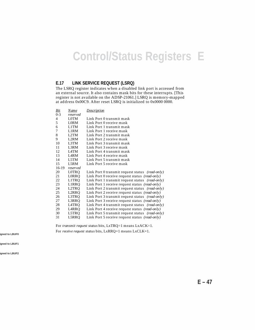
EControl/Status Registers
E – 47
E.17 LINK SERVICE REQUEST (LSRQ)The LSRQ register indicates when a disabled link port is accessed froman external source. It also contains mask bits for these interrupts. [Thisregister is not available on the ADSP-21061.] LSRQ is memory-mappedat address 0x00C9. After reset LSRQ is initialized to 0x0000 0000.
Bit Name Description0-3 reserved4 L0TM Link Port 0 transmit mask5 L0RM Link Port 0 receive mask6 L1TM Link Port 1 transmit mask7 L1RM Link Port 1 receive mask8 L2TM Link Port 2 transmit mask9 L2RM Link Port 2 receive mask10 L3TM Link Port 3 transmit mask11 L3RM Link Port 3 receive mask12 L4TM Link Port 4 transmit mask13 L4RM Link Port 4 receive mask14 L5TM Link Port 5 transmit mask15 L5RM Link Port 5 receive mask16-19 reserved20 L0TRQ Link Port 0 transmit request status (read-only)21 L0RRQ Link Port 0 receive request status (read-only)22 L1TRQ Link Port 1 transmit request status (read-only)23 L1RRQ Link Port 1 receive request status (read-only)24 L2TRQ Link Port 2 transmit request status (read-only)25 L2RRQ Link Port 2 receive request status (read-only)26 L3TRQ Link Port 3 transmit request status (read-only)27 L3RRQ Link Port 3 receive request status (read-only)28 L4TRQ Link Port 4 transmit request status (read-only)29 L4RRQ Link Port 4 receive request status (read-only)30 L5TRQ Link Port 5 transmit request status (read-only)31 L5RRQ Link Port 5 receive request status (read-only)
For transmit request status bits, LxTRQ=1 means LxACK=1.For receive request status bits, LxRRQ=1 means LxCLK=1.
igned to LBUF0
igned to LBUF1
igned to LBUF2
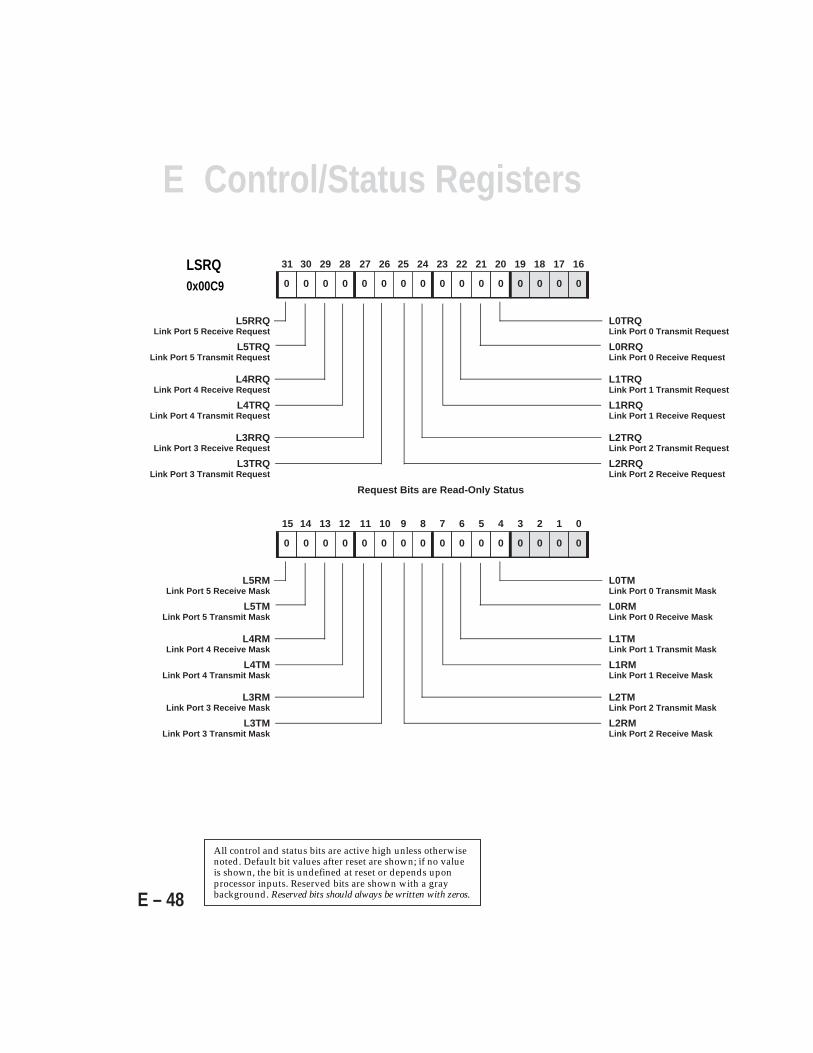
E Control/Status Registers
E – 48
All control and status bits are active high unless otherwisenoted. Default bit values after reset are shown; if no valueis shown, the bit is undefined at reset or depends uponprocessor inputs. Reserved bits are shown with a graybackground. Reserved bits should always be written with zeros.
27 26 25 24 23 22 21 20 19 18 17 1631 30 29 28
11 10 9 8 7 6 5 4 3 2 1 0
000000000000
15 14 13 12
0000
L0TMLink Port 0 Transmit Mask
L0RMLink Port 0 Receive Mask
L1TMLink Port 1 Transmit Mask
L1RMLink Port 1 Receive Mask
L2TMLink Port 2 Transmit Mask
L2RMLink Port 2 Receive Mask
L3RMLink Port 3 Receive Mask
L3TMLink Port 3 Transmit Mask
L4RMLink Port 4 Receive Mask
L4TMLink Port 4 Transmit Mask
L5RMLink Port 5 Receive Mask
L5TMLink Port 5 Transmit Mask
0000000000000000
L0TRQLink Port 0 Transmit Request
L0RRQLink Port 0 Receive Request
L1TRQLink Port 1 Transmit Request
L1RRQLink Port 1 Receive Request
L2TRQLink Port 2 Transmit Request
L2RRQLink Port 2 Receive Request
L3RRQLink Port 3 Receive Request
L3TRQLink Port 3 Transmit Request
L4RRQLink Port 4 Receive Request
L4TRQLink Port 4 Transmit Request
L5RRQLink Port 5 Receive Request
L5TRQLink Port 5 Transmit Request
Request Bits are Read-Only Status
LSRQ0x00C9
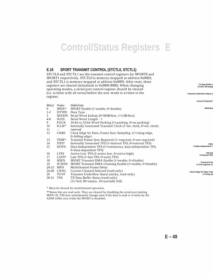
EControl/Status Registers
E – 49
E.18 SPORT TRANSMIT CONTROL (STCTL0, STCTL1)STCTL0 and STCTL1 are the transmit control registers for SPORT0 andSPORT1 respectively. STCTL0 is memory-mapped at address 0x00E0,and STCTL1 is memory-mapped at address 0x00F0. After reset, theseregisters are cleared (initialized to 0x0000 0000). When changingoperating modes, a serial port control register should be cleared(i.e. written with all zeros) before the new mode is written to theregister.
Bit(s) Name Definition0 SPEN* SPORT Enable (1=enable, 0=disable)1-2 DTYPE Data Type3 SENDN Serial Word Endian (0=MSB-first, 1=LSB-first)4-8 SLEN Serial Word Length – 19 PACK 16-bit to 32-bit Word Packing (1=packing, 0=no packing)10 ICLK* Internally Generated Transmit Clock (1=int. clock, 0=ext. clock)11 – reserved12 CKRE Clock Edge for Data, Frame Sync Sampling (1=rising edge,
0=falling edge)13 TFSR* Transmit Frame Sync Required (1=required, 0=not required)14 ITFS* Internally Generated TFS (1=internal TFS, 0=external TFS)15 DITFS Data-Independent TFS (1=continuous, data-independent TFS,
0=data-dependent TFS)16 LTFS Active Low TFS (1=active low, 0=active high)17 LAFS* Late TFS (1=late TFS, 0=early TFS)18 SDEN SPORT Transmit DMA Enable (1=enable, 0=disable)19 SCHEN SPORT Transmit DMA Chaining Enable (1=enable, 0=disable)20-23 MFD Multichannel Frame Delay24-28 CHNL Current Channel Selected (read-only)29 TUVF Transmit Underflow Status (sticky, read-only)30-31 TXS TX Data Buffer Status (read-only)
(11=full, 00=empty, 10=partially full)
* Must be cleared for multichannel operation.** Status bits are read-only. They are cleared by disabling the serial port (settingSPEN=0). TXS may subsequently change state if the data is read or written by theADSP-2106x core while the SPORT is disabled.
Multichan
Current Channel S
Transmit Underflow Status (s
TX Data Buffer S11=full, 00=empty
Data-1=data-independent, 0
Tranmsit Fram1=TFS required, 0=
Clock Edge for Data, Fram1=rising edg
Internal1=internal TDFS

E Control/Status Registers
E – 50
All control and status bits are active high unless otherwisenoted. Default bit values after reset are shown; if no valueis shown, the bit is undefined at reset or depends uponprocessor inputs. Reserved bits are shown with a graybackground. Reserved bits should always be written with zeros.
STCTL0STCTL1
0x00E00x00F0
DTYPE: Normal Operation (Non-Multichannel) DTYPE: Multichannel Operation
DTYPE Data Formatting DTYPE Data Formatting00 Right-justify, zero-fill unused MSBs x0 Right-justify, zero-fill unused MSBs01 Right-justify, sign-extend into unused MSBs x1 Right-justify, sign-extend into unused MSBs10 Compand using µ-law 0x Compand using µ-law11 Compand using A-law 1x Compand using A-law
MCEMultichannel Enable1=enable, 0=disable
NCHNumber of Channels – 1
SPL*SPORT Loopback
1=enable, 0=disableD2DMA*2-Dimensional DMA Array Enable
26 25 24 23 22 21 20 19 18 17
000000000000
31 30 29 28 27
0000
16
LRFSActive Low RFS1=active low, 0=active high
LAFS*Late RFS1=late RFS, 0=early RFS
ROVFReceive Overflow Status (sticky, read-only)
SDENSPORT Receive DMA Enable1=enable DMA, 0=disable DMA
SCHENSPORT Receive DMA Chaining Enable1=enable chaining, 0=disable chaining
RXSRX Data Buffer Status (read-only)
11=full, 00=empty, 10=partially full
11 10 9 8 7 6 5 4 3 2 1 0
00000000000
15 14 13 12
000
SPEN*SPORT Enable1=enable, 0=disable
DTYPEData Type
SENDNSerial Word Endian0=MSB-first, 1=LSB-first
SLENSerial Word Length – 1
PACK16-bit to 32-bit Word Packing1=packing, 0=no packing
IRFSInternally Generated RFS
1=internal RFS, 0=external RFS
RFSR*Receive Frame Sync Required
1=RFS required, 0=RFS not required
CKREClock Edge for Data, Frame Sync Sampling
1=rising edge, 0=falling edge
ICLKInternally Generated Receive Clock1=internal clock, 0=external clock* Must be cleared for multichannel operation.
0 0
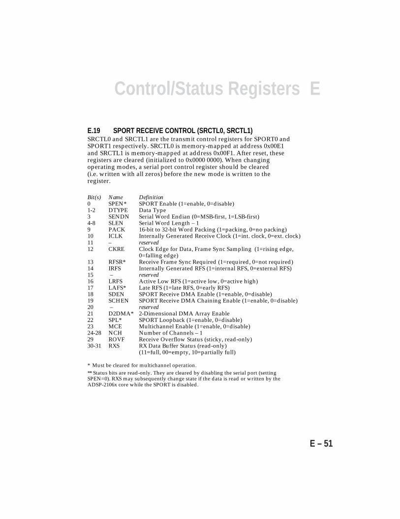
EControl/Status Registers
E – 51
E.19 SPORT RECEIVE CONTROL (SRCTL0, SRCTL1)SRCTL0 and SRCTL1 are the transmit control registers for SPORT0 andSPORT1 respectively. SRCTL0 is memory-mapped at address 0x00E1and SRCTL1 is memory-mapped at address 0x00F1. After reset, theseregisters are cleared (initialized to 0x0000 0000). When changingoperating modes, a serial port control register should be cleared(i.e. written with all zeros) before the new mode is written to theregister.
Bit(s) Name Definition0 SPEN* SPORT Enable (1=enable, 0=disable)1-2 DTYPE Data Type3 SENDN Serial Word Endian (0=MSB-first, 1=LSB-first)4-8 SLEN Serial Word Length – 19 PACK 16-bit to 32-bit Word Packing (1=packing, 0=no packing)10 ICLK Internally Generated Receive Clock (1=int. clock, 0=ext. clock)11 – reserved12 CKRE Clock Edge for Data, Frame Sync Sampling (1=rising edge,
0=falling edge)13 RFSR* Receive Frame Sync Required (1=required, 0=not required)14 IRFS Internally Generated RFS (1=internal RFS, 0=external RFS)15 – reserved16 LRFS Active Low RFS (1=active low, 0=active high)17 LAFS* Late RFS (1=late RFS, 0=early RFS)18 SDEN SPORT Receive DMA Enable (1=enable, 0=disable)19 SCHEN SPORT Receive DMA Chaining Enable (1=enable, 0=disable)20 – reserved21 D2DMA* 2-Dimensional DMA Array Enable22 SPL* SPORT Loopback (1=enable, 0=disable)23 MCE Multichannel Enable (1=enable, 0=disable)24-28 NCH Number of Channels – 129 ROVF Receive Overflow Status (sticky, read-only)30-31 RXS RX Data Buffer Status (read-only)
(11=full, 00=empty, 10=partially full)
* Must be cleared for multichannel operation.** Status bits are read-only. They are cleared by disabling the serial port (settingSPEN=0). RXS may subsequently change state if the data is read or written by theADSP-2106x core while the SPORT is disabled.
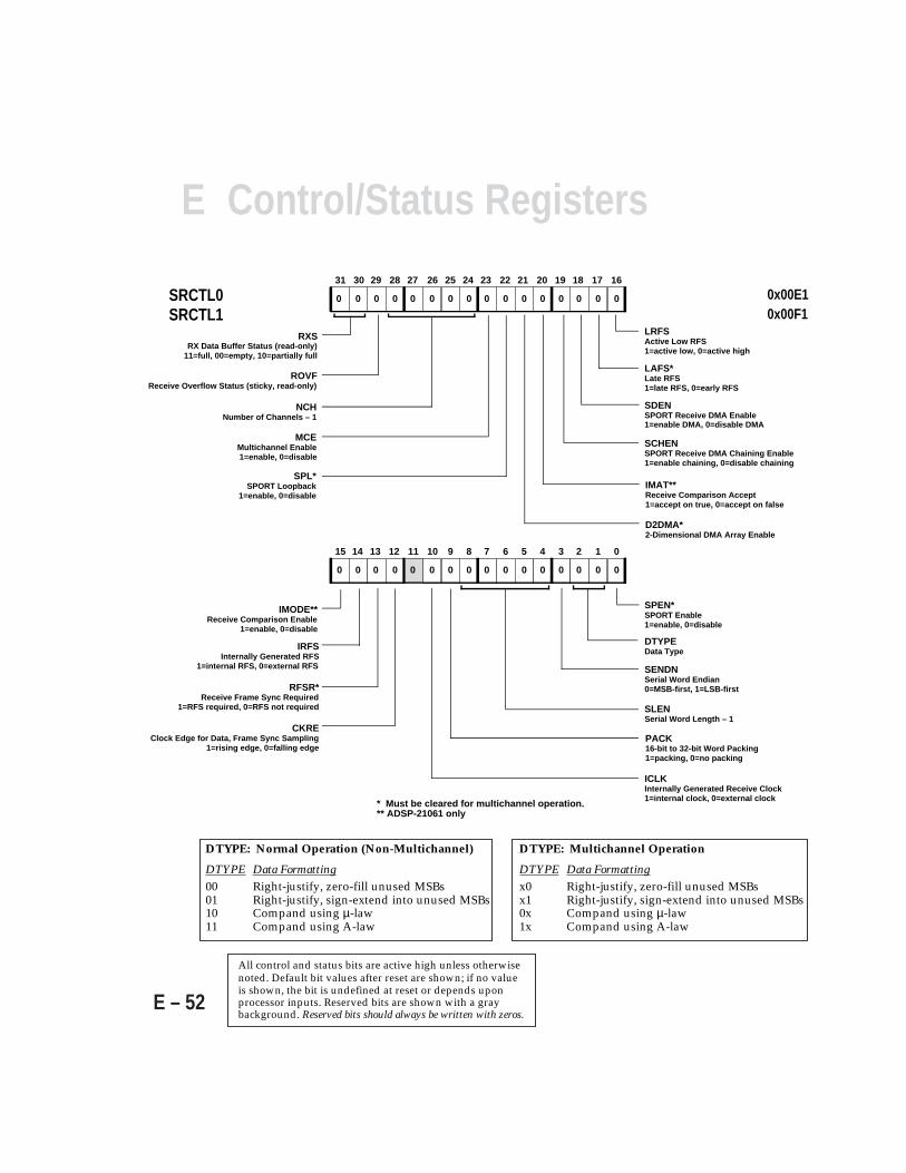
E Control/Status Registers
E – 52
SRCTL0SRCTL1
0x00E10x00F1
All control and status bits are active high unless otherwisenoted. Default bit values after reset are shown; if no valueis shown, the bit is undefined at reset or depends uponprocessor inputs. Reserved bits are shown with a graybackground. Reserved bits should always be written with zeros.
DTYPE: Normal Operation (Non-Multichannel) DTYPE: Multichannel Operation
DTYPE Data Formatting DTYPE Data Formatting00 Right-justify, zero-fill unused MSBs x0 Right-justify, zero-fill unused MSBs01 Right-justify, sign-extend into unused MSBs x1 Right-justify, sign-extend into unused MSBs10 Compand using µ-law 0x Compand using µ-law11 Compand using A-law 1x Compand using A-law
MCEMultichannel Enable1=enable, 0=disable
NCHNumber of Channels – 1
SPL*SPORT Loopback
1=enable, 0=disableIMAT**Receive Comparison Accept1=accept on true, 0=accept on false
26 25 24 23 22 21 20 19 18 17
000000000000
31 30 29 28 27
0000
16
LRFSActive Low RFS1=active low, 0=active high
LAFS*Late RFS1=late RFS, 0=early RFS
ROVFReceive Overflow Status (sticky, read-only)
SDENSPORT Receive DMA Enable1=enable DMA, 0=disable DMA
SCHENSPORT Receive DMA Chaining Enable1=enable chaining, 0=disable chaining
RXSRX Data Buffer Status (read-only)
11=full, 00=empty, 10=partially full
11 10 9 8 7 6 5 4 3 2 1 0
00000000000
15 14 13 12
000
SPEN*SPORT Enable1=enable, 0=disable
DTYPEData Type
SENDNSerial Word Endian0=MSB-first, 1=LSB-first
SLENSerial Word Length – 1
PACK16-bit to 32-bit Word Packing1=packing, 0=no packing
IRFSInternally Generated RFS
1=internal RFS, 0=external RFS
RFSR*Receive Frame Sync Required
1=RFS required, 0=RFS not required
CKREClock Edge for Data, Frame Sync Sampling
1=rising edge, 0=falling edge
ICLKInternally Generated Receive Clock1=internal clock, 0=external clock
* Must be cleared for multichannel operation.** ADSP-21061 only
0 0
D2DMA*2-Dimensional DMA Array Enable
IMODE**Receive Comparison Enable
1=enable, 0=disable
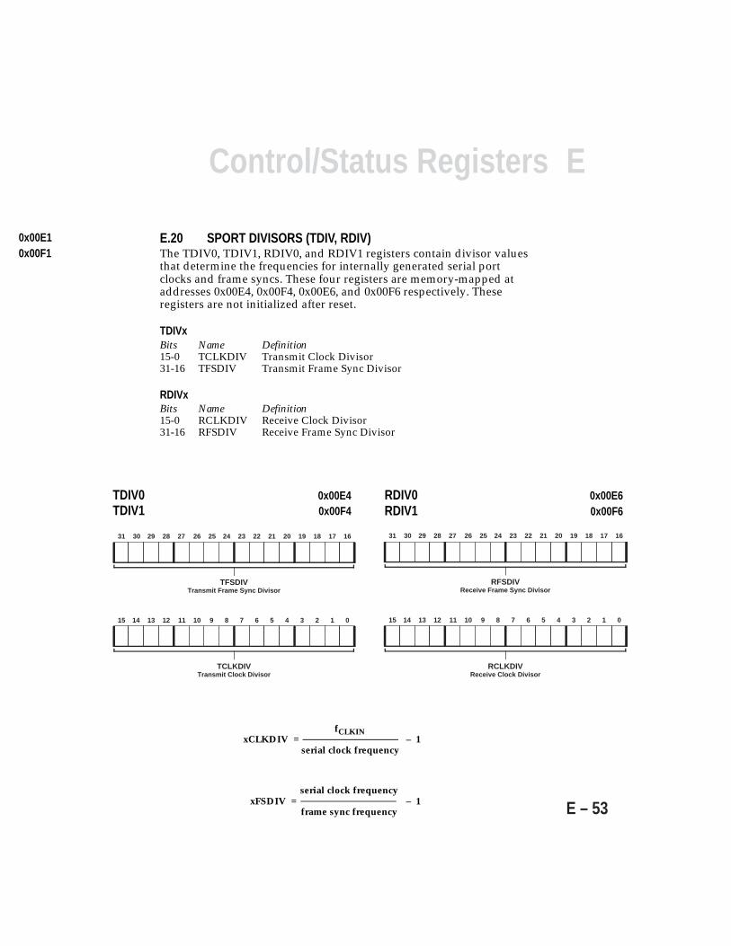
EControl/Status Registers
E – 53
E.20 SPORT DIVISORS (TDIV, RDIV)The TDIV0, TDIV1, RDIV0, and RDIV1 registers contain divisor valuesthat determine the frequencies for internally generated serial portclocks and frame syncs. These four registers are memory-mapped ataddresses 0x00E4, 0x00F4, 0x00E6, and 0x00F6 respectively. Theseregisters are not initialized after reset.
TDIVxBits Name Definition15-0 TCLKDIV Transmit Clock Divisor31-16 TFSDIV Transmit Frame Sync Divisor
RDIVxBits Name Definition15-0 RCLKDIV Receive Clock Divisor31-16 RFSDIV Receive Frame Sync Divisor
serial clock frequencyxFSDIV = – 1
frame sync frequency
fCLKINxCLKDIV = – 1
serial clock frequency
0x00E10x00F1
RDIV0 0x00E6RDIV1 0x00F6
11 10 9 8 7 6 5 4 3 2 1 015 14 13 12
26 25 24 23 22 21 20 19 18 1731 30 29 28 27 16
TCLKDIVTransmit Clock Divisor
TFSDIVTransmit Frame Sync Divisor
TDIV0 0x00E4TDIV1 0x00F4
11 10 9 8 7 6 5 4 3 2 1 015 14 13 12
26 25 24 23 22 21 20 19 18 1731 30 29 28 27 16
RCLKDIVReceive Clock Divisor
RFSDIVReceive Frame Sync Divisor
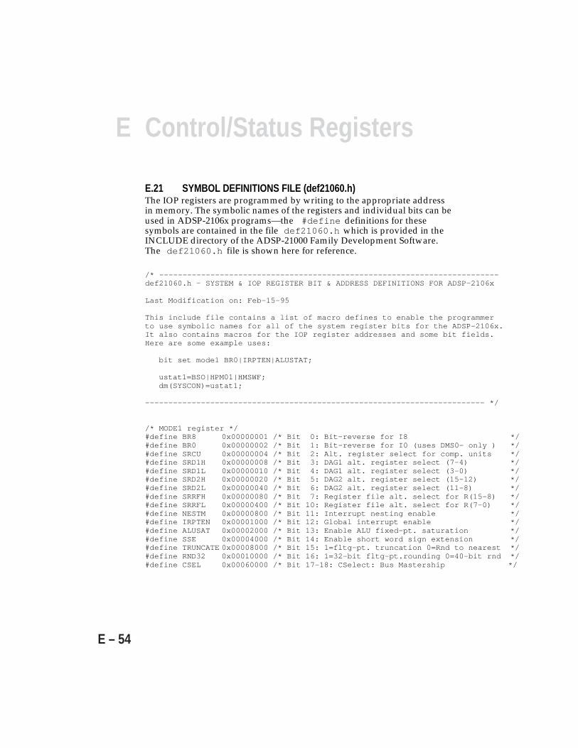
E Control/Status Registers
E – 54
E.21 SYMBOL DEFINITIONS FILE (def21060.h)The IOP registers are programmed by writing to the appropriate addressin memory. The symbolic names of the registers and individual bits can beused in ADSP-2106x programs—the #define definitions for thesesymbols are contained in the file def21060.h which is provided in theINCLUDE directory of the ADSP-21000 Family Development Software.The def21060.h file is shown here for reference.
/* —————————————————————————————————————————————————————————————————————————def21060.h - SYSTEM & IOP REGISTER BIT & ADDRESS DEFINITIONS FOR ADSP-2106x
Last Modification on: Feb-15-95
This include file contains a list of macro defines to enable the programmerto use symbolic names for all of the system register bits for the ADSP-2106x.It also contains macros for the IOP register addresses and some bit fields.Here are some example uses:
bit set mode1 BR0|IRPTEN|ALUSTAT;
ustat1=BSO|HPM01|HMSWF;dm(SYSCON)=ustat1;
————————————————————————————————————————————————————————————————————————— */
/* MODE1 register */#define BR8 0x00000001 /* Bit 0: Bit-reverse for I8 */#define BR0 0x00000002 /* Bit 1: Bit-reverse for I0 (uses DMS0- only ) */#define SRCU 0x00000004 /* Bit 2: Alt. register select for comp. units */#define SRD1H 0x00000008 /* Bit 3: DAG1 alt. register select (7-4) */#define SRD1L 0x00000010 /* Bit 4: DAG1 alt. register select (3-0) */#define SRD2H 0x00000020 /* Bit 5: DAG2 alt. register select (15-12) */#define SRD2L 0x00000040 /* Bit 6: DAG2 alt. register select (11-8) */#define SRRFH 0x00000080 /* Bit 7: Register file alt. select for R(15-8) */#define SRRFL 0x00000400 /* Bit 10: Register file alt. select for R(7-0) */#define NESTM 0x00000800 /* Bit 11: Interrupt nesting enable */#define IRPTEN 0x00001000 /* Bit 12: Global interrupt enable */#define ALUSAT 0x00002000 /* Bit 13: Enable ALU fixed-pt. saturation */#define SSE 0x00004000 /* Bit 14: Enable short word sign extension */#define TRUNCATE 0x00008000 /* Bit 15: 1=fltg-pt. truncation 0=Rnd to nearest */#define RND32 0x00010000 /* Bit 16: 1=32-bit fltg-pt.rounding 0=40-bit rnd */#define CSEL 0x00060000 /* Bit 17-18: CSelect: Bus Mastership */
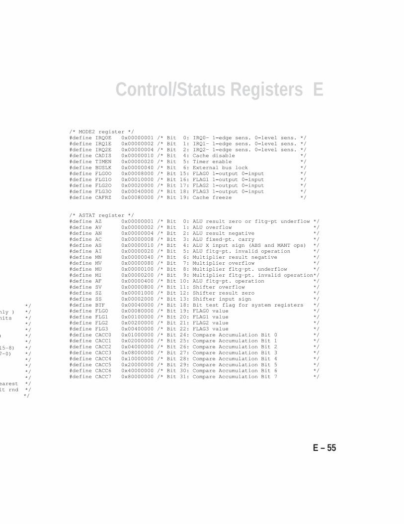
EControl/Status Registers
E – 55
/* MODE2 register */#define IRQ0E 0x00000001 /* Bit 0: IRQ0- 1=edge sens. 0=level sens. */#define IRQ1E 0x00000002 /* Bit 1: IRQ1- 1=edge sens. 0=level sens. */#define IRQ2E 0x00000004 /* Bit 2: IRQ2- 1=edge sens. 0=level sens. */#define CADIS 0x00000010 /* Bit 4: Cache disable */#define TIMEN 0x00000020 /* Bit 5: Timer enable */#define BUSLK 0x00000040 /* Bit 6: External bus lock */#define FLG0O 0x00008000 /* Bit 15: FLAG0 1=output 0=input */#define FLG1O 0x00010000 /* Bit 16: FLAG1 1=output 0=input */#define FLG2O 0x00020000 /* Bit 17: FLAG2 1=output 0=input */#define FLG3O 0x00040000 /* Bit 18: FLAG3 1=output 0=input */#define CAFRZ 0x00080000 /* Bit 19: Cache freeze */
/* ASTAT register */#define AZ 0x00000001 /* Bit 0: ALU result zero or fltg-pt underflow */#define AV 0x00000002 /* Bit 1: ALU overflow */#define AN 0x00000004 /* Bit 2: ALU result negative */#define AC 0x00000008 /* Bit 3: ALU fixed-pt. carry */#define AS 0x00000010 /* Bit 4: ALU X input sign (ABS and MANT ops) */#define AI 0x00000020 /* Bit 5: ALU fltg-pt. invalid operation */#define MN 0x00000040 /* Bit 6: Multiplier result negative */#define MV 0x00000080 /* Bit 7: Multiplier overflow */#define MU 0x00000100 /* Bit 8: Multiplier fltg-pt. underflow */#define MI 0x00000200 /* Bit 9: Multiplier fltg-pt. invalid operation*/#define AF 0x00000400 /* Bit 10: ALU fltg-pt. operation */#define SV 0x00000800 /* Bit 11: Shifter overflow */#define SZ 0x00001000 /* Bit 12: Shifter result zero */#define SS 0x00002000 /* Bit 13: Shifter input sign */#define BTF 0x00040000 /* Bit 18: Bit test flag for system registers */#define FLG0 0x00080000 /* Bit 19: FLAG0 value */#define FLG1 0x00100000 /* Bit 20: FLAG1 value */#define FLG2 0x00200000 /* Bit 21: FLAG2 value */#define FLG3 0x00400000 /* Bit 22: FLAG3 value */#define CACC0 0x01000000 /* Bit 24: Compare Accumulation Bit 0 */#define CACC1 0x02000000 /* Bit 25: Compare Accumulation Bit 1 */#define CACC2 0x04000000 /* Bit 26: Compare Accumulation Bit 2 */#define CACC3 0x08000000 /* Bit 27: Compare Accumulation Bit 3 */#define CACC4 0x10000000 /* Bit 28: Compare Accumulation Bit 4 */#define CACC5 0x20000000 /* Bit 29: Compare Accumulation Bit 5 */#define CACC6 0x40000000 /* Bit 30: Compare Accumulation Bit 6 */#define CACC7 0x80000000 /* Bit 31: Compare Accumulation Bit 7 */
*/nly ) */nits */ */ */
) */ */15-8) */7-0) */ */ */ */ */earest */it rnd */ */
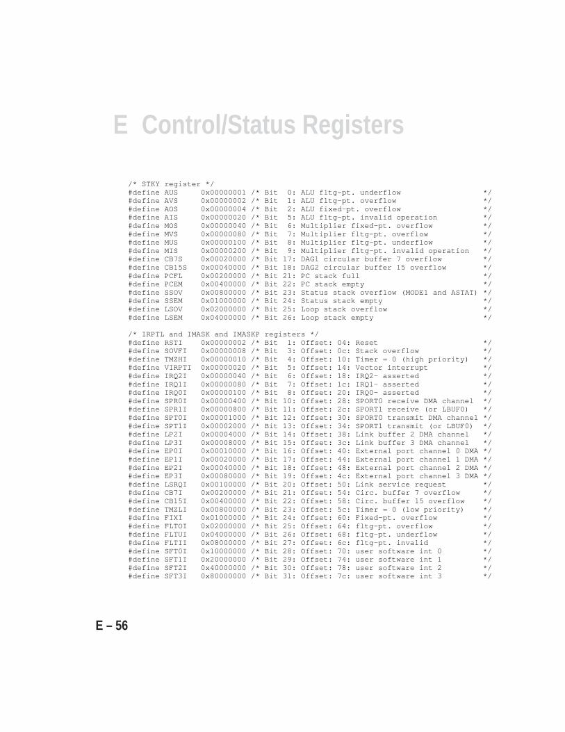
E Control/Status Registers
E – 56
/* STKY register */#define AUS 0x00000001 /* Bit 0: ALU fltg-pt. underflow */#define AVS 0x00000002 /* Bit 1: ALU fltg-pt. overflow */#define AOS 0x00000004 /* Bit 2: ALU fixed-pt. overflow */#define AIS 0x00000020 /* Bit 5: ALU fltg-pt. invalid operation */#define MOS 0x00000040 /* Bit 6: Multiplier fixed-pt. overflow */#define MVS 0x00000080 /* Bit 7: Multiplier fltg-pt. overflow */#define MUS 0x00000100 /* Bit 8: Multiplier fltg-pt. underflow */#define MIS 0x00000200 /* Bit 9: Multiplier fltg-pt. invalid operation */#define CB7S 0x00020000 /* Bit 17: DAG1 circular buffer 7 overflow */#define CB15S 0x00040000 /* Bit 18: DAG2 circular buffer 15 overflow */#define PCFL 0x00200000 /* Bit 21: PC stack full */#define PCEM 0x00400000 /* Bit 22: PC stack empty */#define SSOV 0x00800000 /* Bit 23: Status stack overflow (MODE1 and ASTAT) */#define SSEM 0x01000000 /* Bit 24: Status stack empty */#define LSOV 0x02000000 /* Bit 25: Loop stack overflow */#define LSEM 0x04000000 /* Bit 26: Loop stack empty */
/* IRPTL and IMASK and IMASKP registers */#define RSTI 0x00000002 /* Bit 1: Offset: 04: Reset */#define SOVFI 0x00000008 /* Bit 3: Offset: 0c: Stack overflow */#define TMZHI 0x00000010 /* Bit 4: Offset: 10: Timer = 0 (high priority) */#define VIRPTI 0x00000020 /* Bit 5: Offset: 14: Vector interrupt */#define IRQ2I 0x00000040 /* Bit 6: Offset: 18: IRQ2- asserted */#define IRQ1I 0x00000080 /* Bit 7: Offset: 1c: IRQ1- asserted */#define IRQ0I 0x00000100 /* Bit 8: Offset: 20: IRQ0- asserted */#define SPR0I 0x00000400 /* Bit 10: Offset: 28: SPORT0 receive DMA channel */#define SPR1I 0x00000800 /* Bit 11: Offset: 2c: SPORT1 receive (or LBUF0) */#define SPT0I 0x00001000 /* Bit 12: Offset: 30: SPORT0 transmit DMA channel */#define SPT1I 0x00002000 /* Bit 13: Offset: 34: SPORT1 transmit (or LBUF0) */#define LP2I 0x00004000 /* Bit 14: Offset: 38: Link buffer 2 DMA channel */#define LP3I 0x00008000 /* Bit 15: Offset: 3c: Link buffer 3 DMA channel */#define EP0I 0x00010000 /* Bit 16: Offset: 40: External port channel 0 DMA */#define EP1I 0x00020000 /* Bit 17: Offset: 44: External port channel 1 DMA */#define EP2I 0x00040000 /* Bit 18: Offset: 48: External port channel 2 DMA */#define EP3I 0x00080000 /* Bit 19: Offset: 4c: External port channel 3 DMA */#define LSRQI 0x00100000 /* Bit 20: Offset: 50: Link service request */#define CB7I 0x00200000 /* Bit 21: Offset: 54: Circ. buffer 7 overflow */#define CB15I 0x00400000 /* Bit 22: Offset: 58: Circ. buffer 15 overflow */#define TMZLI 0x00800000 /* Bit 23: Offset: 5c: Timer = 0 (low priority) */#define FIXI 0x01000000 /* Bit 24: Offset: 60: Fixed-pt. overflow */#define FLTOI 0x02000000 /* Bit 25: Offset: 64: fltg-pt. overflow */#define FLTUI 0x04000000 /* Bit 26: Offset: 68: fltg-pt. underflow */#define FLTII 0x08000000 /* Bit 27: Offset: 6c: fltg-pt. invalid */#define SFT0I 0x10000000 /* Bit 28: Offset: 70: user software int 0 */#define SFT1I 0x20000000 /* Bit 29: Offset: 74: user software int 1 */#define SFT2I 0x40000000 /* Bit 30: Offset: 78: user software int 2 */#define SFT3I 0x80000000 /* Bit 31: Offset: 7c: user software int 3 */
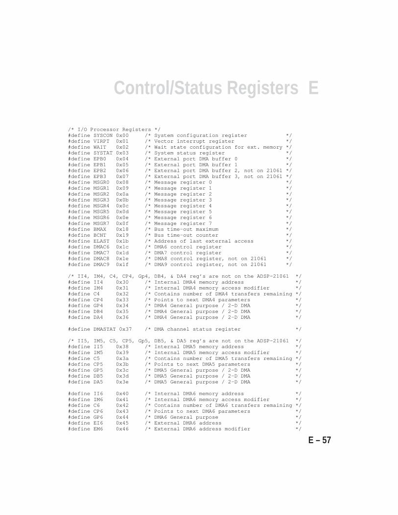
EControl/Status Registers
E – 57
/* I/O Processor Registers */#define SYSCON 0x00 /* System configuration register */#define VIRPT 0x01 /* Vector interrupt register */#define WAIT 0x02 /* Wait state configuration for ext. memory */#define SYSTAT 0x03 /* System status register */#define EPB0 0x04 /* External port DMA buffer 0 */#define EPB1 0x05 /* External port DMA buffer 1 */#define EPB2 0x06 /* External port DMA buffer 2, not on 21061 */#define EPB3 0x07 /* External port DMA buffer 3, not on 21061 */#define MSGR0 0x08 /* Message register 0 */#define MSGR1 0x09 /* Message register 1 */#define MSGR2 0x0a /* Message register 2 */#define MSGR3 0x0b /* Message register 3 */#define MSGR4 0x0c /* Message register 4 */#define MSGR5 0x0d /* Message register 5 */#define MSGR6 0x0e /* Message register 6 */#define MSGR7 0x0f /* Message register 7 */#define BMAX 0x18 /* Bus time-out maximum */#define BCNT 0x19 /* Bus time-out counter */#define ELAST 0x1b /* Address of last external access */#define DMAC6 0x1c /* DMA6 control register */#define DMAC7 0x1d /* DMA7 control register */#define DMAC8 0x1e /* DMA8 control register, not on 21061 */#define DMAC9 0x1f /* DMA9 control register, not on 21061 */
/* II4, IM4, C4, CP4, Gp4, DB4, & DA4 reg’s are not on the ADSP-21061 */#define II4 0x30 /* Internal DMA4 memory address */#define IM4 0x31 /* Internal DMA4 memory access modifier */#define C4 0x32 /* Contains number of DMA4 transfers remaining */#define CP4 0x33 /* Points to next DMA4 parameters */#define GP4 0x34 /* DMA4 General purpose / 2-D DMA */#define DB4 0x35 /* DMA4 General purpose / 2-D DMA */#define DA4 0x36 /* DMA4 General purpose / 2-D DMA */
#define DMASTAT 0x37 /* DMA channel status register */
/* II5, IM5, C5, CP5, Gp5, DB5, & DA5 reg’s are not on the ADSP-21061 */#define II5 0x38 /* Internal DMA5 memory address */#define IM5 0x39 /* Internal DMA5 memory access modifier */#define C5 0x3a /* Contains number of DMA5 transfers remaining */#define CP5 0x3b /* Points to next DMA5 parameters */#define GP5 0x3c /* DMA5 General purpose / 2-D DMA */#define DB5 0x3d /* DMA5 General purpose / 2-D DMA */#define DA5 0x3e /* DMA5 General purpose / 2-D DMA */
#define II6 0x40 /* Internal DMA6 memory address */#define IM6 0x41 /* Internal DMA6 memory access modifier */#define C6 0x42 /* Contains number of DMA6 transfers remaining */#define CP6 0x43 /* Points to next DMA6 parameters */#define GP6 0x44 /* DMA6 General purpose */#define EI6 0x45 /* External DMA6 address */#define EM6 0x46 /* External DMA6 address modifier */

E Control/Status Registers
E – 58
#define EC6 0x47 /* External DMA6 counter */
#define II7 0x48 /* Internal DMA7 memory address */#define IM7 0x49 /* Internal DMA7 memory access modifier */#define C7 0x4a /* Contains number of DMA7 transfers remaining */#define CP7 0x4b /* Points to next DMA7 parameters */#define GP7 0x4c /* DMA7 General purpose */#define EI7 0x4d /* External DMA7 address */#define EM7 0x4e /* External DMA7 address modifier */#define EC7 0x4f /* External DMA7 counter */
/* II8, IM8, C8, CP8, Gp8, EI8, EM8, & EC8 reg’s are not on the 21061 */#define II8 0x50 /* Internal DMA8 memory address */#define IM8 0x51 /* Internal DMA8 memory access modifier */#define C8 0x52 /* Contains number of DMA8 transfers remaining */#define CP8 0x53 /* Points to next DMA8 parameters */#define GP8 0x54 /* DMA8 General purpose */#define EI8 0x55 /* External DMA8 address */#define EM8 0x56 /* External DMA8 address modifier */#define EC8 0x57 /* External DMA8 counter */
/* II9, IM9, C9, CP9, Gp9, EI9, EM9, & EC9 reg’s are not on the 21061 */#define II9 0x58 /* Internal DMA9 memory address */#define IM9 0x59 /* Internal DMA9 memory access modifier */#define C9 0x5a /* Contains number of DMA9 transfers remaining */#define CP9 0x5b /* Points to next DMA9 parameters */#define GP9 0x5c /* DMA9 General purpose */#define EI9 0x5d /* External DMA9 address */#define EM9 0x5e /* External DMA9 address modifier */#define EC9 0x5f /* External DMA9 counter */
#define II0 0x60 /* Internal DMA0 memory address */#define IM0 0x61 /* Internal DMA0 memory access modifier */#define C0 0x62 /* Contains number of DMA0 transfers remaining */#define CP0 0x63 /* Points to next DMA0 parameters */#define GP0 0x64 /* DMA0 General purpose / 2-D DMA */#define DB0 0x65 /* DMA0 General purpose / 2-D DMA, not on 21061 */#define DA0 0x66 /* DMA0 General purpose / 2-D DMA, not on 21061 */
#define II2 0x70 /* Internal DMA2 memory address */#define IM2 0x71 /* Internal DMA2 memory access modifier */#define C2 0x72 /* Contains number of DMA2 transfers remaining */#define CP2 0x73 /* Points to next DMA2 parameters */#define GP2 0x74 /* DMA2 General purpose / 2-D DMA */#define DB2 0x75 /* DMA2 General purpose / 2-D DMA, not on 21061 */#define DA2 0x76 /* DMA2 General purpose / 2-D DMA, not on 21061 */
#define II1 0x68 /* Internal DMA1 memory address */#define IM1 0x69 /* Internal DMA1 memory access modifier */#define C1 0x6a /* Contains number of DMA1 transfers remaining */#define CP1 0x6b /* Points to next DMA1 parameters */
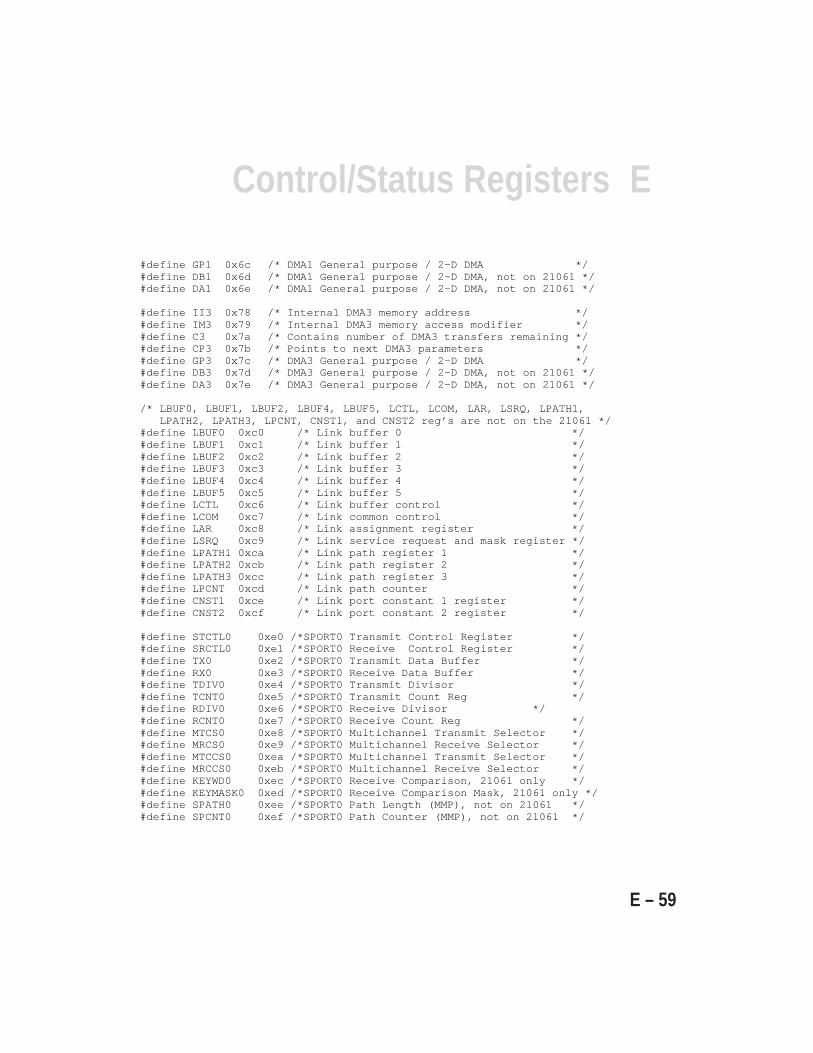
EControl/Status Registers
E – 59
#define GP1 0x6c /* DMA1 General purpose / 2-D DMA */#define DB1 0x6d /* DMA1 General purpose / 2-D DMA, not on 21061 */#define DA1 0x6e /* DMA1 General purpose / 2-D DMA, not on 21061 */
#define II3 0x78 /* Internal DMA3 memory address */#define IM3 0x79 /* Internal DMA3 memory access modifier */#define C3 0x7a /* Contains number of DMA3 transfers remaining */#define CP3 0x7b /* Points to next DMA3 parameters */#define GP3 0x7c /* DMA3 General purpose / 2-D DMA */#define DB3 0x7d /* DMA3 General purpose / 2-D DMA, not on 21061 */#define DA3 0x7e /* DMA3 General purpose / 2-D DMA, not on 21061 */
/* LBUF0, LBUF1, LBUF2, LBUF4, LBUF5, LCTL, LCOM, LAR, LSRQ, LPATH1, LPATH2, LPATH3, LPCNT, CNST1, and CNST2 reg’s are not on the 21061 */#define LBUF0 0xc0 /* Link buffer 0 */#define LBUF1 0xc1 /* Link buffer 1 */#define LBUF2 0xc2 /* Link buffer 2 */#define LBUF3 0xc3 /* Link buffer 3 */#define LBUF4 0xc4 /* Link buffer 4 */#define LBUF5 0xc5 /* Link buffer 5 */#define LCTL 0xc6 /* Link buffer control */#define LCOM 0xc7 /* Link common control */#define LAR 0xc8 /* Link assignment register */#define LSRQ 0xc9 /* Link service request and mask register */#define LPATH1 0xca /* Link path register 1 */#define LPATH2 0xcb /* Link path register 2 */#define LPATH3 0xcc /* Link path register 3 */#define LPCNT 0xcd /* Link path counter */#define CNST1 0xce /* Link port constant 1 register */#define CNST2 0xcf /* Link port constant 2 register */
#define STCTL0 0xe0 /*SPORT0 Transmit Control Register */#define SRCTL0 0xe1 /*SPORT0 Receive Control Register */#define TX0 0xe2 /*SPORT0 Transmit Data Buffer */#define RX0 0xe3 /*SPORT0 Receive Data Buffer */#define TDIV0 0xe4 /*SPORT0 Transmit Divisor */#define TCNT0 0xe5 /*SPORT0 Transmit Count Reg */#define RDIV0 0xe6 /*SPORT0 Receive Divisor */#define RCNT0 0xe7 /*SPORT0 Receive Count Reg */#define MTCS0 0xe8 /*SPORT0 Multichannel Transmit Selector */#define MRCS0 0xe9 /*SPORT0 Multichannel Receive Selector */#define MTCCS0 0xea /*SPORT0 Multichannel Transmit Selector */#define MRCCS0 0xeb /*SPORT0 Multichannel Receive Selector */#define KEYWD0 0xec /*SPORT0 Receive Comparison, 21061 only */#define KEYMASK0 0xed /*SPORT0 Receive Comparison Mask, 21061 only */#define SPATH0 0xee /*SPORT0 Path Length (MMP), not on 21061 */#define SPCNT0 0xef /*SPORT0 Path Counter (MMP), not on 21061 */

E Control/Status Registers
E – 60
#define STCTL1 0xf0 /*SPORT1 Transmit Control Register */#define SRCTL1 0xf1 /*SPORT1 Receive Control Register */#define TX1 0xf2 /*SPORT1 Transmit Data Buffer */#define RX1 0xf3 /*SPORT1 Receive Data Buffer */#define TDIV1 0xf4 /*SPORT1 Transmit Divisor */#define TCNT1 0xf5 /*SPORT1 Transmit Count Reg */#define RDIV1 0xf6 /*SPORT1 Receive Divisor */#define RCNT1 0xf7 /*SPORT1 Receive Count Reg */#define MTCS1 0xf8 /*SPORT1 Multichannel Transmit Selector */#define MRCS1 0xf9 /*SPORT1 Multichannel Receive Selector */#define MTCCS1 0xfa /*SPORT1 Multichannel Transmit Selector */#define MRCCS1 0xfb /*SPORT1 Multichannel Receive Selector*/#define KEYWD1 0xfc /*SPORT1 Receive Comparison, 21061 only */#define KEYMASK1 0xfd /*SPORT1 Receive Comparison Mask, 21061 only */#define SPATH1 0xfe /*SPORT1 Path Length (MMP), not on 21061 */#define SPCNT1 0xff /*SPORT1 Path Counter (MMP), not on 21061 */
/* SYSCON Register */#define SYSCON 0x00 /* System Configuration Register */#define SRST 0x00000001 /* Soft Reset */#define BSO 0x00000002 /* Boot Select Override */#define IIVT 0x00000004 /* Internal Interrupt Vector Table */#define IWT 0x00000008 /* Instruction word transfer (0=data,1=instr) */#define HPM00 0x00000000 /* Host packing mode: None */#define HPM01 0x00000010 /* Host packing mode: 16/32 */#define HPM10 0x00000020 /* Host packing mode: 16/48 */#define HPM11 0x00000030 /* Host packing mode: 32/48 */#define HMSWF 0x00000040 /* Host packing order (0=LSW-first, 1=MSW-first) */#define HPFLSH 0x00000080 /* Host pack flush */#define IMDW0X 0x00000100 /* Internal memory block 0, extended data (40-bit) */#define IMDW1X 0x00000200 /* Internal memory block 1, extended data (40-bit) */#define EBPR00 0x00000000 /* External bus priority: Even */#define EBPR01 0x00010000 /* External bus priority: Core has priority */#define EBPR10 0x00020000 /* External bus priority: IO has priority */#define DCPR 0x00040000 /* Select rotating access priority on DMA6 - DMA9 */#define IMGR 0x10000000 /* Internal memory block grouping (mesh multiproc) */
/* SYSTAT Register */#define SYSTAT 0x03 /* System Status Register */#define HSTM 0x00000001 /* Host is the Bus Master */#define BSYN 0x00000002 /* Bus arbitration logic is synchronized */#define CRBM 0x00000070 /* Current ADSP2106x Bus Master */#define IDC 0x00000700 /* ADSP2106x ID Code */#define DWPD 0x00001000 /* Direct write pending (0=none, 1=pending) */#define VIPD 0x00002000 /* Vector interrupt pending (1=pending) */#define HPS 0x0000c000 /* Host packing status */
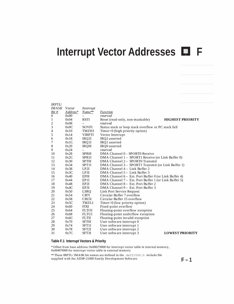
F
F – 1
Interrupt Vector Addresses
IRPTL/IMASK Vector InterruptBit # Address* Name** Function0 0x00 – reserved1 0x04 RSTI Reset (read-only, non-maskable) HIGHEST PRIORITY2 0x08 – reserved3 0x0C SOVFI Status stack or loop stack overflow or PC stack full4 0x10 TMZHI Timer=0 (high priority option)5 0x14 VIRPTI Vector Interrupt6 0x18 IRQ2I IRQ2 asserted7 0x1C IRQ1I IRQ1 asserted8 0x20 IRQ0I IRQ0 asserted9 0x24 – reserved10 0x28 SPR0I DMA Channel 0 – SPORT0 Receive11 0x2C SPR1I DMA Channel 1 – SPORT1 Receive (or Link Buffer 0)12 0x30 SPT0I DMA Channel 2 – SPORT0 Transmit13 0x34 SPT1I DMA Channel 3 – SPORT1 Transmit (or Link Buffer 1)14 0x38 LP2I DMA Channel 4 – Link Buffer 215 0x3C LP3I DMA Channel 5 – Link Buffer 316 0x40 EP0I DMA Channel 6 – Ext. Port Buffer 0 (or Link Buffer 4)17 0x44 EP1I DMA Channel 7 – Ext. Port Buffer 1 (or Link Buffer 5)18 0x48 EP2I DMA Channel 8 – Ext. Port Buffer 219 0x4C EP3I DMA Channel 9 – Ext. Port Buffer 320 0x50 LSRQ Link Port Service Request21 0x54 CB7I Circular Buffer 7 overflow22 0x58 CB15I Circular Buffer 15 overflow23 0x5C TMZLI Timer=0 (low priority option)24 0x60 FIXI Fixed-point overflow25 0x64 FLTOI Floating-point overflow exception26 0x68 FLTUI Floating-point underflow exception27 0x6C FLTII Floating-point invalid exception28 0x70 SFT0I User software interrupt 029 0x74 SFT1I User software interrupt 130 0x78 SFT2I User software interrupt 231 0x7C SFT3I User software interrupt 3 LOWEST PRIORITY
Table F.1 Interrupt Vectors & Priority
* Offset from base address: 0x0002 0000 for interrupt vector table in internal memory,0x0040 0000 for interrupt vector table in external memory** These IRPTL/IMASK bit names are defined in the def21060.h include filesupplied with the ADSP-21000 Family Development Software.
F Interrupt Vector Addresses
F – 2
Table F.1 shows all ADSP-2106x interrupts, listed according their bitposition in the IRPTL and IMASK registers. Also shown is the addressof the interrupt vector; each vector is separated by eight memorylocations. The addresses in the vector table represent offsets from abase address. For an interrupt vector table in internal memory, thebase address is 0x0002 0000; for an interrupt vector table in externalmemory, the base address is 0x0040 0000. The third column in TableF.1 lists a mnemonic name for each interrupt. These names areprovided for convenience, and are not required by the assembler.
The interrupt vector table may be located in internal memory, ataddress 0x0002 0000 (the beginning of Block 0), or in external memoryat address 0x0040 0000. If the ADSP-2106x’s on-chip memory is bootedfrom an external source, the interrupt vector table will be located ininternal memory. If, however, the ADSP-2106x is not booted (becauseit will execute from off-chip memory), the vector table must be locatedin the off-chip memory. See “Booting” in the System Design chapter fordetails on booting mode selection. Also, if booting is from an externalEPROM or host processor, bit 16 of IMASK (the EP0I interrupt forDMA Channel 6) will automatically be set to 1 following reset—thisenables the DMA done interrupt for Channel 6. IRPTL is initialized toall zeros following reset.
The IIVT bit in the SYSCON control register can be used to overridethe booting mode in determining where the interrupt vector table islocated. If the ADSP-2106x is not booted (no boot mode), setting IIVT to1 selects an internal vector table while IIVT=0 selects an external vectortable. If the ADSP-2106x is booted from an external source (any modeother than no boot mode), then IIVT has no effect.
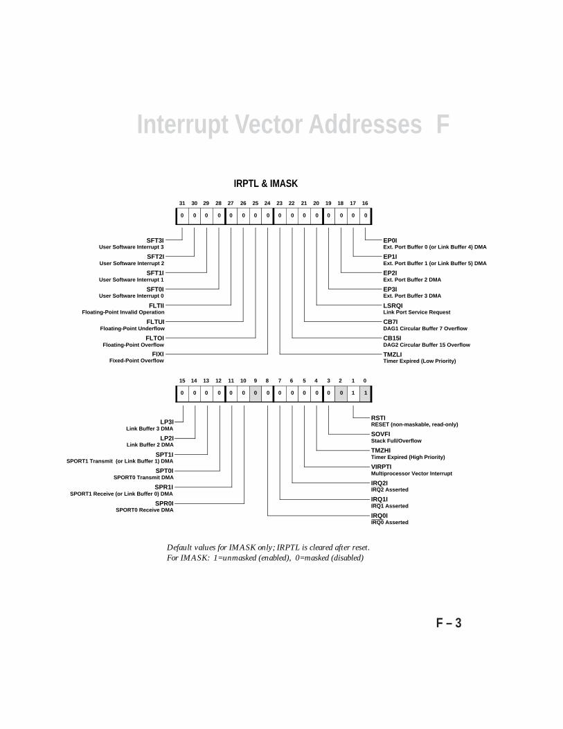
FInterrupt Vector Addresses
F – 3
Default values for IMASK only; IRPTL is cleared after reset.For IMASK: 1=unmasked (enabled), 0=masked (disabled)
IRPTL & IMASK
11 10 9 8 7 6 5 4 3 2 1 015 14 13 12
0 0 0 0 0 0 0 0 0 0 0 0 0 0 1 1
SPR0ISPORT0 Receive DMA
RSTIRESET (non-maskable, read-only)
SOVFIStack Full/Overflow
TMZHITimer Expired (High Priority)
VIRPTIMultiprocessor Vector Interrupt
IRQ2IIRQ2 Asserted
IRQ1IIRQ1 Asserted
IRQ0IIRQ0 Asserted
SPR1ISPORT1 Receive (or Link Buffer 0) DMA
SPT0ISPORT0 Transmit DMA
SPT1ISPORT1 Transmit (or Link Buffer 1) DMA
LP2ILink Buffer 2 DMA
LP3ILink Buffer 3 DMA
26 25 24 23 22 21 20 19 18 1731 30 29 28 27 16
0 0 0 0 0 0 0 0 0 0 0 0 0 0 0 0
EP0IExt. Port Buffer 0 (or Link Buffer 4) DMA
LSRQILink Port Service Request
CB7IDAG1 Circular Buffer 7 Overflow
CB15IDAG2 Circular Buffer 15 Overflow
TMZLITimer Expired (Low Priority)
EP1IExt. Port Buffer 1 (or Link Buffer 5) DMA
EP2IExt. Port Buffer 2 DMA
EP3IExt. Port Buffer 3 DMA
FLTUIFloating-Point Underflow
FLTIIFloating-Point Invalid Operation
FLTOIFloating-Point Overflow
FIXIFixed-Point Overflow
SFT0IUser Software Interrupt 0
SFT1IUser Software Interrupt 1
SFT2IUser Software Interrupt 2
SFT3IUser Software Interrupt 3

F Interrupt Vector Addresses
F – 4
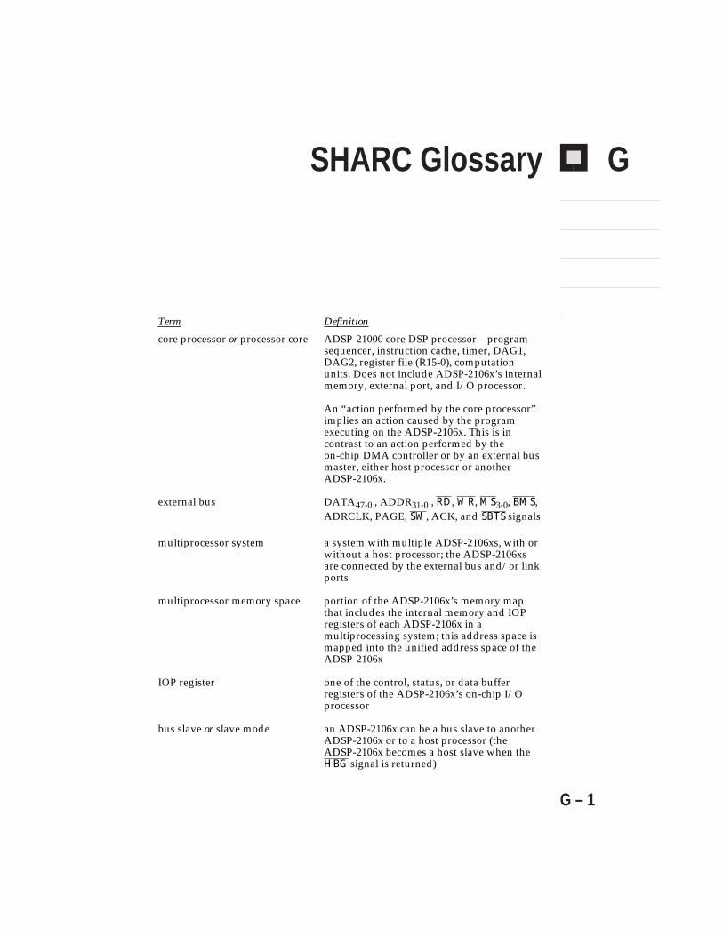
G
G – 1
SHARC Glossary
Term Definition
core processor or processor core ADSP-21000 core DSP processor—programsequencer, instruction cache, timer, DAG1,DAG2, register file (R15-0), computationunits. Does not include ADSP-2106x’s internalmemory, external port, and I/O processor.
An “action performed by the core processor”implies an action caused by the programexecuting on the ADSP-2106x. This is incontrast to an action performed by theon-chip DMA controller or by an external busmaster, either host processor or anotherADSP-2106x.
external bus DATA47-0 , ADDR31-0 , RD, WR, MS3-0, BMS,ADRCLK, PAGE, SW, ACK, and SBTS signals
multiprocessor system a system with multiple ADSP-2106xs, with orwithout a host processor; the ADSP-2106xsare connected by the external bus and/or linkports
multiprocessor memory space portion of the ADSP-2106x’s memory mapthat includes the internal memory and IOPregisters of each ADSP-2106x in amultiprocessing system; this address space ismapped into the unified address space of theADSP-2106x
IOP register one of the control, status, or data bufferregisters of the ADSP-2106x’s on-chip I/Oprocessor
bus slave or slave mode an ADSP-2106x can be a bus slave to anotherADSP-2106x or to a host processor (theADSP-2106x becomes a host slave when theHBG signal is returned)

G SHARC Glossary
G – 2
bus transition cycle (BTC) a cycle in which control of the external bus ispassed from one ADSP-2106x to another (in amultiprocessor system)
host transition cycle (HTC) a cycle in which control of the external bus ispassed from the ADSP-2106x to the hostprocessor—during this cycle the ADSP-2106xstops driving the RD, WR, ADDR31-0, MS3-0,ADRCLK, PAGE, SW, and DMAGx signals,which must then be driven by the host
asynchronous transfers asynchronous host accesses of the ADSP-2106x;after acquiring control of the ADSP-2106x’sexternal bus, the host must assert the CS pin ofthe ADSP-2106x it wants to access; theADSP-2106x uses the REDY output to add waitstates to an asynchronous access
synchronous transfers synchronous host accesses of the ADSP-2106x;CS is not asserted and the host must act likeanother ADSP-2106x in a multiprocessorsystem, by generating an address inmultiprocessor memory space, asserting WR orRD, and driving out or latching in the data; theADSP-2106x uses ACK to add wait states to asynchronous access
direct reads & writes a direct access of the ADSP-2106x’s internalmemory or IOP registers by anotherADSP-2106x or by a host processor
external port FIFO buffers EPB0, EPB1, EPB2, and EPB3—the IOPregisters used for external port DMA transfersand single-word data transfers (from otherADSP-2106xs or from a host processor); thesebuffers are 6-deep FIFOs
single-word data transfers reads and writes to the EPBx external portbuffers, performed externally by theADSP-2106x bus master or internally by theADSP-2106x slave’s core; these occur whenDMA is disabled in the DMACx controlregister
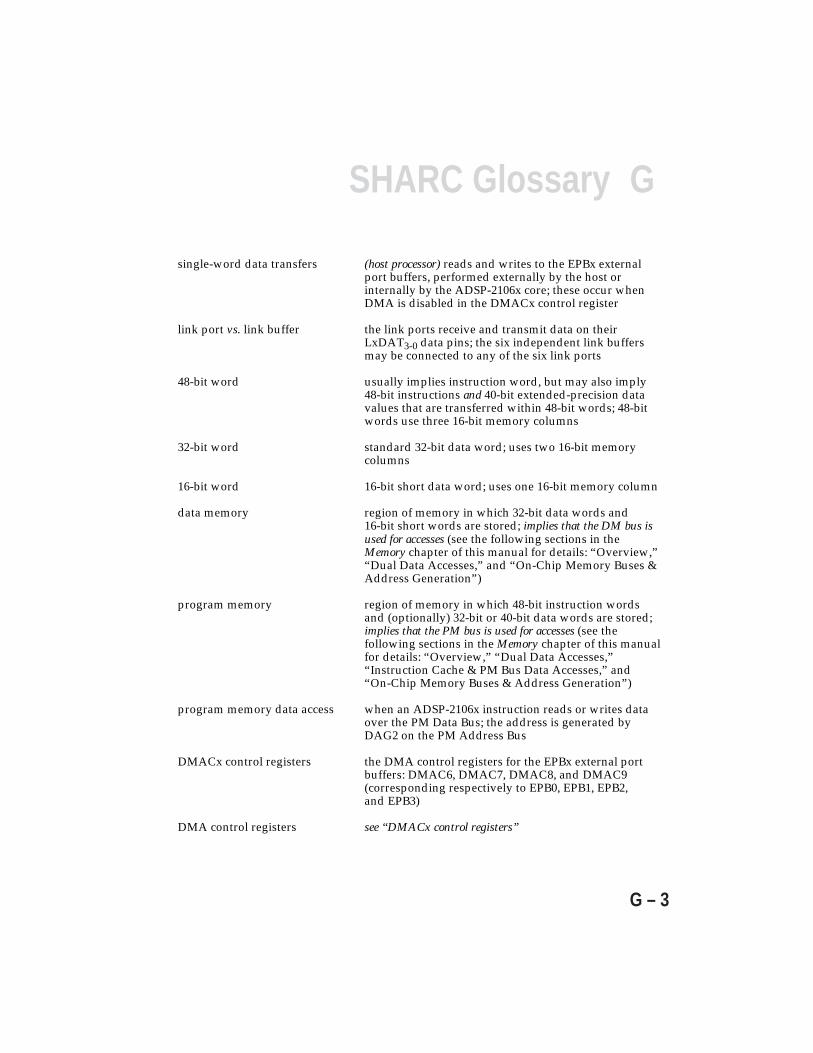
GSHARC Glossary
G – 3
single-word data transfers (host processor) reads and writes to the EPBx externalport buffers, performed externally by the host orinternally by the ADSP-2106x core; these occur whenDMA is disabled in the DMACx control register
link port vs. link buffer the link ports receive and transmit data on theirLxDAT3-0 data pins; the six independent link buffersmay be connected to any of the six link ports
48-bit word usually implies instruction word, but may also imply48-bit instructions and 40-bit extended-precision datavalues that are transferred within 48-bit words; 48-bitwords use three 16-bit memory columns
32-bit word standard 32-bit data word; uses two 16-bit memorycolumns
16-bit word 16-bit short data word; uses one 16-bit memory column
data memory region of memory in which 32-bit data words and16-bit short words are stored; implies that the DM bus isused for accesses (see the following sections in theMemory chapter of this manual for details: “Overview,”“Dual Data Accesses,” and “On-Chip Memory Buses &Address Generation”)
program memory region of memory in which 48-bit instruction wordsand (optionally) 32-bit or 40-bit data words are stored;implies that the PM bus is used for accesses (see thefollowing sections in the Memory chapter of this manualfor details: “Overview,” “Dual Data Accesses,”“Instruction Cache & PM Bus Data Accesses,” and“On-Chip Memory Buses & Address Generation”)
program memory data access when an ADSP-2106x instruction reads or writes dataover the PM Data Bus; the address is generated byDAG2 on the PM Address Bus
DMACx control registers the DMA control registers for the EPBx external portbuffers: DMAC6, DMAC7, DMAC8, and DMAC9(corresponding respectively to EPB0, EPB1, EPB2,and EPB3)
DMA control registers see “DMACx control registers”
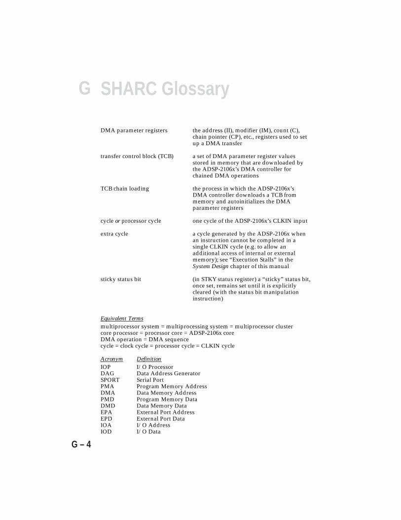
G SHARC Glossary
G – 4
DMA parameter registers the address (II), modifier (IM), count (C),chain pointer (CP), etc., registers used to setup a DMA transfer
transfer control block (TCB) a set of DMA parameter register valuesstored in memory that are downloaded bythe ADSP-2106x’s DMA controller forchained DMA operations
TCB chain loading the process in which the ADSP-2106x’sDMA controller downloads a TCB frommemory and autoinitializes the DMAparameter registers
cycle or processor cycle one cycle of the ADSP-2106x’s CLKIN input
extra cycle a cycle generated by the ADSP-2106x whenan instruction cannot be completed in asingle CLKIN cycle (e.g. to allow anadditional access of internal or externalmemory); see “Execution Stalls” in theSystem Design chapter of this manual
sticky status bit (in STKY status register) a “sticky” status bit,once set, remains set until it is explicitlycleared (with the status bit manipulationinstruction)
Equivalent Termsmultiprocessor system = multiprocessing system = multiprocessor clustercore processor = processor core = ADSP-2106x coreDMA operation = DMA sequencecycle = clock cycle = processor cycle = CLKIN cycle
Acronym DefinitionIOP I/O ProcessorDAG Data Address GeneratorSPORT Serial PortPMA Program Memory AddressDMA Data Memory AddressPMD Program Memory DataDMD Data Memory DataEPA External Port AddressEPD External Port DataIOA I/O AddressIOD I/O Data
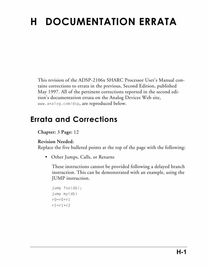
H DOCUMENTATION ERRATA
This revision of the ADSP-2106x SHARC Processor User’s Manual con-tains corrections to errata in the previous, Second Edition, published May 1997. All of the pertinent corrections reported in the second edi-tion’s documentation errata on the Analog Devices Web site, www.analog.com/dsp, are reproduced below.
Errata and CorrectionsChapter: 3 Page: 12
Revision Needed:Replace the five bulleted points at the top of the page with the following:
• Other Jumps, Calls, or Returns
These instructions cannot be provided following a delayed branch instruction. This can be demonstrated with an example, using the JUMP instruction.
jump foo(db);
jump my(db)
r0=r0+r1
r1=r1+r2
H-1

Errata and Corrections
In this case, the delayed branch instruction R0=R0+R1; is executed but the instruction R1=R1+R2 is not executed. Also, the control jumps to my instead of foo, with the delayed branch instruction being the execution of foo.
The exception is for JUMP, which can be done for mutually-exclu-sive conditions for both (EQ, NE). If the first EQ condition works, then the NE conditional jump has no meaning; it is as good as a NOP. Code for these exceptions is shown below:
if eq jump label1 (db);
if ne jump label2 (db);
nop;
nop;
• Pushes or Pops of the PC stack
Push of the PC stack in the delayed branch is followed by a pop. If a value is pushed in the delayed branch of call, it is popped first in the called subroutine, which is followed by return to subroutine RTS.
For example:
20119 call foo (db);
2011A push PCSTK;
2011B nop;
2011C foo;
PCSTK 2011B: second push due to PCSTK2011C: first push due to call
This demonstrates that when the user pushes the PCSTK during a delayed slot, the PC stack pointer is pushed onto the PCSTK.
H-2
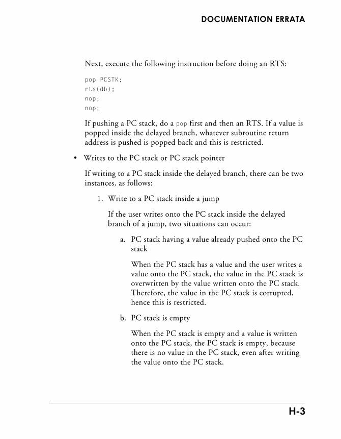
DOCUMENTATION ERRATA
Next, execute the following instruction before doing an RTS:
pop PCSTK;
rts(db);
nop;
nop;
If pushing a PC stack, do a pop first and then an RTS. If a value is popped inside the delayed branch, whatever subroutine return address is pushed is popped back and this is restricted.
• Writes to the PC stack or PC stack pointer
If writing to a PC stack inside the delayed branch, there can be two instances, as follows:
1. Write to a PC stack inside a jump
If the user writes onto the PC stack inside the delayed branch of a jump, two situations can occur:
a. PC stack having a value already pushed onto the PC stack
When the PC stack has a value and the user writes a value onto the PC stack, the value in the PC stack is overwritten by the value written onto the PC stack. Therefore, the value in the PC stack is corrupted, hence this is restricted.
b. PC stack is empty
When the PC stack is empty and a value is written onto the PC stack, the PC stack is empty, because there is no value in the PC stack, even after writing the value onto the PC stack.
H-3

Errata and Corrections
2. Write to a PC stack inside a call
If the user writes to the PC stack inside a call, the value pushed onto the PC stack due to a call is overwritten by the value written onto the PC stack. Hence, when the user does an RTS, the user returns to the address pushed onto the PC stack and not to the address pushed while branching to the subroutine.
For example:
[20111] call foo3(db);
[20112] PCSTK=0x2011C;
[20113] nop;
[20114]
The value 20114 is pushed onto the PC stack, while the value 2011C is written to the PC stack. Accordingly, the value 20114 is overwritten by 2011C in the PC stack. Thus, when the user comes back by doing an RTS, the return is to the address 2011C and not to 20114. Consequently, this is restricted.
• DO UNTIL instruction
If a loop is present inside the delayed branch, it performs a sequen-tial operation after executing the loop and does not jump to the label. This happens because the address of the destination of the jump is flushed out of the pipeline. Instead, in the pipeline (Fetch, Decode, and Execute) are the instructions of the loop, which causes sequential operation.
H-4

DOCUMENTATION ERRATA
For example:
20118 LCNTR=10;
20119 jump my(db); 2012C my:
2011A do my until LCE;
2011B my: r0=r0+r1;
2011C r2=r2+r3;
2011D r1=r1+r2;
In the example, there is a loop inside a delayed branch. Because the loop executes the instructions inside the loop ten times, the address of the destination of the jump (2012C) is flushed. After that, instead of going to label my (2012C), the processor executes the next sequential instruction at address 2011C and then continues the sequential execution. This is the reason why loop is restricted inside the delayed branch.
• IDLE instruction
To come out of the idle instruction, an interrupt is needed. If the user puts an IDLE instruction inside the delayed branch, the pro-cessor is always in the idle state, unless there is an interrupt, hence this instruction is restricted.
Chapter: 3 Page: 21
Revision Needed:In the third paragraph, third sentence, the segment “8-instructionintervals” should be replaced with “4-instruction intervals.”
H-5
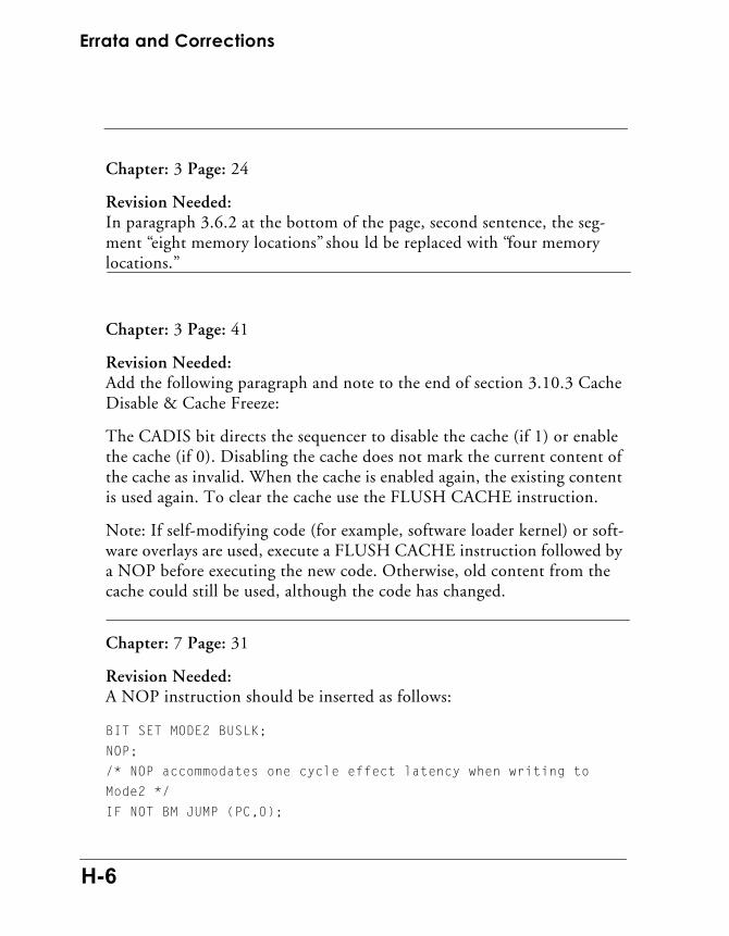
Errata and Corrections
Chapter: 3 Page: 24
Revision Needed:In paragraph 3.6.2 at the bottom of the page, second sentence, the seg-ment “eight memory locations” shou ld be replaced with “four memory locations.”
Chapter: 3 Page: 41
Revision Needed:Add the following paragraph and note to the end of section 3.10.3 Cache Disable & Cache Freeze:
The CADIS bit directs the sequencer to disable the cache (if 1) or enable the cache (if 0). Disabling the cache does not mark the current content of the cache as invalid. When the cache is enabled again, the existing content is used again. To clear the cache use the FLUSH CACHE instruction.
Note: If self-modifying code (for example, software loader kernel) or soft-ware overlays are used, execute a FLUSH CACHE instruction followed by a NOP before executing the new code. Otherwise, old content from the cache could still be used, although the code has changed.
Chapter: 7 Page: 31
Revision Needed:A NOP instruction should be inserted as follows:
BIT SET MODE2 BUSLK;
NOP;
/* NOP accommodates one cycle effect latency when writing to
Mode2 */
IF NOT BM JUMP (PC,0);
H-6

DOCUMENTATION ERRATA
Chapter: 7 Page: 31
Revision Needed:The instruction IF NE JUMP (PC,-2); should be replaced with IF TF JUMP (PC,-2);
Chapter: 8 Page: 8
Revision Needed: The last paragraph on this page is confusing. It should be changed to:
Table 8.2 covers all cases including various multiprocessing systems. There is a special case for a single ADSP-2106x system where id=0. In this scenario, the host needs to drive only the ADDR18–0 pins.
Chapter: 10 Page: 18
Revision Needed:Add the following statement to the third paragraph of the Companding section:
Program the SPORT registers prior to loading data values into the SPORT buffers for companding to execute properly.
Chapter: A Page: 5
Revision Needed:The condition labeled NBM is incorrect syntax. The correct syntax for the condition is NOT BM.
H-7
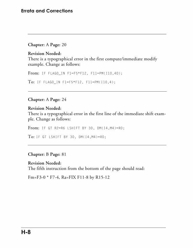
Errata and Corrections
Chapter: A Page: 20
Revision Needed:There is a typographical error in the first compute/immediate modify example. Change as follows:
From: IF FLAG0_IN F1=F5*F12, F11=PM(I10,40);
To: IF FLAG0_IN F1=F5*F12, F11=PM(I10,4);
Chapter: A Page: 24
Revision Needed:There is a typographical error in the first line of the immediate shift exam-ple. Change as follows:
From: IF GT R2=R6 LSHIFT BY 30, DM(I4,M4)=R0;
To: IF GT LSHIFT BY 30, DM(I4,M4)=R0;
Chapter: B Page: 81
Revision Needed:The fifth instruction from the bottom of the page should read:
Fm=F3-0 * F7-4, Ra=FIX F11-8 by R15-12
H-8

DOCUMENTATION ERRATA
Chapter: E Page: 50
Revision Needed: The bit fields shown are for the SPORT Receive Control register, not the Transmit Control register. See Figure 10.2 on page 10-10 for the correct bit fields of the Transmit Control register.
Chapter: E Page: 51
Revision Needed:Bit 20 of the SRCTLx register is incorrectly marked as being reserved. See page E-52 for the correct bit description.
Chapter: F Page: 2
Revision Needed:In the first paragraph, second sentence, the segment “eight memory loca-tions” should be replaced with “four memory locations.”
H-9

Errata and Corrections
H-10
Index
X – 1X – 1
Index
Symbolsµ-law companding ................................. 10-1816-bit data .......................................... 4-4, 5-1316-bit floating-point data
2-3, B-74, B-75, C-316-bit short words .................. 4-4, 6-14, 6-212-dimensional DMA ........................ 9-9, E-433.3V components .................................... 11-2532-bit words ............................................. 11-4340-bit data ...................... 1-5, 2-3, 5-34, 6-38,
........................................... 8-29, 9-15, C-248-bit words ............................................. 11-43
AA-law companding ................................ 10-18A/D converters ........................................... 1-7ABS ............................................................... 2-7AC flag ................................................. 2-9, 3-8ACK ....... 5-39, 6-41, 6-46, 7-21, 7-22, 7-23,
........... 7-24, 7-25, 7-26, 8-9, 8-12, 8-14,................ 8-15, 8-16, 11-8, 11-22, 11-29,......................................... 11-40, E-32, G-2
Active drive output .................................. 8-10Adaptive filtering ....................................... 1-7Address modifiers ...................................... 4-6Address pointer wraparound ................... 1-9Address pointers ........................................ 1-9ADSP-21000 Family Development
Software ......................... 3-25, E-4, E-54ADSP-21060 ............................ 1-4, 1-12, E-18ADSP-21062 ....... 1-4, 1-12, 5-14, 5-16, E-18AF flag .......................................................... 2-9AI flag ........................................................... 2-9AIS flag ................................................ 2-8, 2-9Alternate (secondary) registers
................................. 1-11, 2-27, 2-28, 4-3Alternate register select ............................. 4-4ALU carry .................................................... 3-8ALU fixed-point carry ............................... 2-7ALU fixed-point overflow ...................... E-20ALU flags ................................................... 2-26ALU floating-point overflow ................. E-20ALU input operands .................................. 2-6ALU operations .......................................... B-2ALU overflow .......................... 2-7, 3-8, E-18ALU overflow flag ..................................... 2-7ALU results ................................................. 2-6
ALU saturation ....... 2-6, B-4, B-5, B-6, B-7,............................. B-10, B-11, B-12, B-13,......................................... B-14, B-15, B-37
ALU status flags ......................................... 2-7ALUSAT bit (MODE1 register) ........ 2-6, 2-7AN flag ..................................... 2-8, B-9, B-29AOS flag ....................................................... 2-8Arithmetic exceptions ........... 1-5, 3-21, 3-22Arithmetic interrupts ............................... 3-27Arithmetic precision (RND32 bit) .......... 5-34Arithmetic status ................................ 2-4, 3-7Arithmetic status flags ............................... 3-5AS flag .......................................................... 2-9Assembler .......... 2-1, 3-12, 4-12, 11-41, F-2Assembly language .................................... 2-1ASTAT register ..... 2-7, 2-8, 2-9, 2-15, 2-16,
........................... 2-24, 3-5, 3-7, 3-9, 3-21,..................... 3-22, 3-29, 11-12, E-3, E-55
Asynchronous accesses .................. 8-3, 8-25,................................................... 11-5, 11-46
Asynchronous host accesses ................... 6-41Asynchronous inputs ............................. 11-11Asynchronous interrupts ........................ 3-32Asynchronous transfers ....... 8-1, 8-6, 11-33,
..................................................... E-26, G-2Asynchronous writes ............................... 8-31AUS flag ....................................................... 2-8AV flag ................................................. 2-8, 3-8AVS flag ....................................................... 2-8AZ flag ......................... 2-8, 11-42, B-9, B-29
BB registers ........................................ 4-1, 11-41Background MR register (MRB) ............. 2-12Base address ................................................ 4-1BCNT register ........................................... 7-15BHD bit (SYSCON register) ......... 6-42, 8-18,
........................................ 9-16, 10-8, 10-36BIT CLR instruction ................................... E-3BIT SET instruction ............... 3-29, E-3, E-54Bit test flag (BTF) . 3-7, 3-8, A-46, E-3, E-18BIT TGL instruction ................................... E-3BIT TST instruction ........................... 3-7, E-3BIT XOR instruction ................................... 3-7Bit-reversed addressing .......... 4-1, 4-4, 4-10Bit6 field ..................................................... 2-20BITREV instruction ....................... 4-10, A-48Blocked condition .......................... 6-43, 6-46BMAX register .......................................... 7-15
Index
X – 2
BMS ............... 5-39, 5-42, 11-31, 11-35, E-24Board-level testing ................................. 11-15Boot EPROM ............................................. E-24Booting ..................... 3-26, 3-28, 11-27, E-34Booting mode .............................................. F-2Bootstrapping ............................. 11-29, 11-31Boundary scan ............................... 11-13, D-1BR0 bit ........................................................ 4-10BR8 bit ........................................................ 4-10Branch ........................................ 3-6, 3-9, 3-24Broadcast write ............ 5-18, 7-7, 7-30, 7-31Broadcast write timing ............................ 7-24BRx ............................................... 7-9, 8-3, 8-6BSDL file ..................................................... D-2BSO bit (SYSCON register) ................... 11-31BSYN bit (SYSTAT register) .................... 7-20Buffer base address .................................... 4-1Buffer hang disable (BHD) .......... 6-42, 8-18,
................... 9-16, 10-8, 10-36, E-24, E-28Buffer status .............. 7-27, 9-14, 9-16, 9-19,
....... 10-7, 10-36, E-28, E-37, E-45, E-49Bus arbitration timing .............................. 7-12Bus exchange .............................................. A-6Bus idle cycle ....................... 5-40, 5-41, 5-43,
.................................................. 11-40, E-33Bus lock ........................................... 8-38, E-16Bus master ............................. 7-16, 7-18, 7-19Bus master condition (BM) .... 3-7, 3-8, E-14Bus mastership .......................................... 7-11Bus request prioritization ............. 6-26, 7-11Bus slave .................................................... 3-24Bus synchronization ................................ E-30Bus timeout ............................................... 7-16Bus transition cycle ...... 7-11, 7-18, 8-6, 8-7,
..................................................... 8-11, G-2BUSLK bit (MODE2 register) .................. 7-30Bypass capacitors ................................... 11-25
CC Compiler ............................................... A-54CACC ........................................................... 2-9Cache disable .................................. 3-41, E-16Cache flush ............................................... A-50Cache freeze .................................... 3-41, E-16Cache miss ................. 3-38, 3-39, 3-40, 3-41,
................................................. 11-39, 11-44Cache-inefficient code .............................. 3-40CADIS (cache enable/disable) ............... 3-41CAFRZ (cache freeze) .............................. 3-41
CALL instruction ..................... 3-6, 3-9, 3-15Capacitive loading ................................. 11-22Carry flag ..................................................... 2-9CB15I interrupt ......................................... 3-25CB7I interrupt ........................................... 3-25CCITT G.711 specification ..................... 10-18Chain insertion mode ................... 6-10, 6-32,
..................................................... 6-34, 6-35Chain pointer .................................. 6-23, 6-30Chain pointer register (CP) 6-22, 6-24, 6-28,
.......................................... 6-29, 6-32, 6-35Chained DMA ..................... 6-10, 6-22, 6-28,
.................................................... 6-29, E-39Chained DMA sequences ........................ 6-31Circuit board layout ............................... 11-18Circular buffer addressing ........................ 4-6Circular buffer base address ............. 4-1, 4-6Circular buffer interrupts ............... 3-25, 4-8Circular buffer overflow ...... 3-21, 3-25, 4-8,
...................................................... 4-9, E-22Circular buffer placement ......................... 1-6Circular buffers ... 1-9, 4-1, 4-6, 11-41, E-20Clear interrupt (CI) ............... 3-26, 3-30, A-5Clipping ....................................................... 2-9CLKIN ............................. 11-10, 11-17, 11-18Clock distribution ...................... 11-16, 11-26Clock frequencies ................................... 11-18Clock jitter ............................................... 11-19Clock oscillators ...................................... 11-26Clock skew .................................. 11-16, 11-19Clock tree ................................................. 11-16Cluster multiprocessing ............................ 7-4CMOS input ............................................ 11-17Coefficients .................................................. 5-4Companding ................... 10-17, 10-25, 10-29Compare accumulation (CACC) ...... 2-7, 2-9Compare flags ............................................. 2-9Compare operations .......................... 2-7, 2-9Complex data ............................................ 1-17Complex math .......................................... 2-13Compute field ............................................. B-1Compute operations .................................. B-1Condition codes ................................ 3-8, A-5Condition complements ............................ 3-7Conditional instructions ................ 3-7, 7-10,
....................................................... A-1, E-3Conditional memory read instruction .. 5-49Conditional memory write
instruction .................... 5-37, 5-38, 5-50
Index
X – 3
Context switching1-8, 1-9, 1-11, 2-12, 2-28, 4-3
Core priority access (CPA) ........................ 7-9Core processor ............ 1-8, 1-11, 7-16, 7-17,
........................ 7-21, 8-13, E-2, E-36, G-1Core processor access ................ 11-32, 11-46Core processor buses ............................... 1-10Core processor priority ........................... E-29Count register (C) ............... 6-21, 6-24, 6-33,
.................................................. 6-35, 11-30Counter-based loops .......... 3-15, 3-16, 3-17,
........................................ 3-19, 3-20, 11-40CRBM bits (SYSTAT register) ...... 7-11, 7-19Crossbar bus switch ................................... 1-1Crosstalk ...................................... 11-24, 11-25CS ... 8-8, 8-9, 8-16, 8-34, 11-33, 11-35, G-2Current bus master .................................. E-30Current loop count ..................................... 3-5Current loop counter (CURLCNTR) ...... 3-5,
...................... 3-7, 3-15, 3-19, 3-20, A-36
DDADDR ........................................................ 3-5DAG register transfers ............................ 4-11DAG register transfer restrictions .......... 4-12DAG registers .................... 11-40, 11-41, A-7DAG1 ... 5-3, 5-4, 5-5, 5-8, 5-9, 11-43, E-20DAG1 bit-reversing .................................. 4-10DAG1 registers ... 4-2, 4-3, 4-11, 4-12, A-48DAG2 ....... 1-9, 3-4, 3-9, 3-38, 5-3, 5-4, 5-5,
........................ 5-8, 5-9, 11-43, E-20, G-3DAG2 bit-reversing .................................. 4-10DAG2 registers ... 4-2, 4-3, 4-11, 4-12, A-48Damping resistance ................................ 11-22Data address generators .................. 3-9, A-6Data buffer ...................................... 6-23, 6-29Data memory .......... 11-42, A-40, A-41, G-3Data packing ............. 1-13, 1-15, 5-35, 6-14,
............ 6-22, 6-36, 8-5, 8-10, 8-19, 8-26,............................... 9-9, 10-16, E-43, E-49
Data register file ......................................... 1-8Data registers .................................... 2-6, 2-27Data structures ............................................ 1-9Data word width ...................................... E-27DCPR bit (SYSCON register) .................. 6-26Deadlock resolution ......................... 8-7, 8-13Decode address ........................................... 3-5def21060.h file ................................ 3-25, E-54Delay ........................................................ 11-22
Delay lines ................................................... 1-9Delayed branch (DB) ............ 3-9, 3-10, 3-11,
........................... 3-12, 3-24, 11-38, 11-40,............................. A-5, A-28, A-30, A-34
Denormal operands ......................... 2-3, 2-16Development tools ................................... 1-18Digital filters ................. 1-9, 1-10, 5-4, 11-43Direct addressing ................. 1-11, A-7, A-40Direct branch ............................................... 3-9Direct reads ............... 6-25, 11-46, E-26, G-2Direct reads and writes ........................... 7-26Direct write buffer .................................... 7-22Direct write pending ............................... E-31Direct writes ............ 6-25, 7-34, 8-33, 11-46,
..................................................... E-26, G-2DM Address bus .............. 4-1, 4-2, 4-4, 5-36DM bus .... 5-5, 5-8, 5-19, 7-21, 8-13, 11-42,
........... 11-43, 11-45, E-8, E-9, E-29, G-3DM bus addresses ...................................... 5-9DM Data bus ...... 2-27, 4-11, 5-6, 6-36, 8-18DMA ................................................ 9-13, 9-16DMA (two-dimensional) ........................... 6-7DMA address generation . 6-22, 6-24, 11-45DMA buffer ............................................. 11-45DMA buffer registers ................................. E-8DMA chaining .......... 6-10, 6-22, 6-25, 6-33,
................. 8-14, 10-15, 10-16, E-31, E-39DMA chaining enable bit
(CHEN) .................................. 6-28, E-34DMA channel 1 ......................................... 6-17DMA channel 3 ......................................... 6-17DMA channel 6 ..... 3-26, 6-17, 11-27, 11-30,
................................................. 11-32, 11-34DMA channel 6 interrupt (EP0I) 11-31, 11-33DMA channel 6-9 priority ....................... E-24DMA channel 7 ......................................... 6-17DMA channel parameter registers ......... 6-30DMA channel prioritization ................... 6-48DMA channels ........... 6-20, 6-21, 6-22, E-36DMA controller ..... 1-12, 1-13, 11-27, 11-30,
.................................................... 11-31, G-1DMA count register ............. 6-28, 6-33, 6-35DMA cycle ................................................. 6-21DMA enable ................................................ 9-7DMA enable bit (DEN) .......... 6-6, 6-9, 6-35,
.................... 7-27, 8-19, E-34, E-41, E-49DMA handshake ....... 5-41, 6-12, 6-43, 6-45,
.......................................... 6-48, 8-39, E-32DMA interrupt priority ........................... 6-26DMA interrupt vectors ............................ 6-33
Index
X – 4
DMA interrupts .......... 3-37, 6-6, 6-22, 6-23,............ 6-28, 6-47, 7-27, 8-19, 9-5, 9-17,...... 9-19, 9-23, 10-4, 10-7, 10-36, 10-39,................................................. 10-41, 11-31
DMA master mode ................................... 6-38DMA mode of operation .... 6-13, 6-39, E-38DMA parameter registers ............ 6-20, 6-22,
........ 6-23, 6-24, 11-30, 11-45, E-57, G-4DMA parameters ...................................... 6-28DMA programming, .....................7-23, 10-33,
................................................. 10-37, 10-41DMA request counter .............................. 6-43DMA request latency ............................... 6-44DMA sequence ..................... 6-20, 6-22, 6-28DMA slave mode ...................................... 6-38DMA status ............................................... 6-19DMA subchain .......................................... 6-32DMA throughput, ....................................11-46DMA transfers ....................... 3-37, E-8, E-28DMA word counter ............ 6-13, 6-22, 6-24,
.......................................... 6-34, 6-39, E-38DMAC6 register ......................... 11-27, 11-34DMACx control registers ..... 6-9, 6-37, 7-27DMAGx ........... 6-40, 6-43, 6-44, 6-45, 6-46,
.......................................... 6-47, 6-50, 6-51DMARx ............ 6-13, 6-39, 6-40, 6-42, 6-43,
6-44, 6-45, 6-46, 6-47, 6-50, 6-51, E-38DMASTAT register ....................... E-36, E-39DO FOREVER ............................................. 3-7DO UNTIL instruction ....... 3-13, 3-18, 3-19,
..................................................... 3-20, A-5DO UNTIL loop .......................................... 3-5DRAM ................................... 5-45, 5-46, 5-47DRAM controller ...................................... 11-8DRAM page faults .................................... 5-47DRAM page size ....................................... 5-44Dual add/subtract .................................... 2-26Dual-data-access instructions .......... 5-3, 5-4,
................................................. 11-38, 11-43Dual-ported memory ................................. 5-1DWPD (direct write pending) bit 7-23, 7-34Dynamic range .......................... 1-7, 2-3, C-4
EE field ....................................... 5-11, 8-8, 8-12Early frame syncs ................................... 10-23EC (external count) register 6-22, 6-24, 6-38,
..................................................... 6-41, 6-47Edge-sensitive interrupts ........................ 3-31
Effect latency ...................................... 3-5, E-2EI (external index) register ..................... 6-22,
..................... 6-24, 6-38, 6-41, 6-47, 6-51ELAST ........................................................ 5-45EM (external modify) register ............... 6-22,
..................... 6-24, 6-38, 6-41, 6-47, 6-51EM register ................................................ 6-47EP0I interrupt ....................... 3-25, 3-26, 3-28EP1I interrupt ........................................... 3-25EP2I interrupt ........................................... 3-25EP3I interrupt ........................................... 3-25EPA bus (external port address) ...... 6-3, 8-2EPBx buffer status .................................... E-37EPBx buffers .... 6-11, 6-12, 6-13, 6-36, 6-37,
..................... 6-39, 6-40, 6-41, 6-46, 6-51,
.......................................... 7-26, 8-18, E-38EPD bus (external port data) ................... 6-3,
.................................. 6-36, 7-26, 8-2, 8-18EPROM booting ........................................ 5-39Error handling ............................................ 1-7Exception conditions .................................. 2-4Exception handling ............................ 1-5, 2-4Execute address .......................................... 3-5Exponent extract operations (EXP) 2-19, 2-24Extended-precision data ......................... 5-34,
................................. 6-38, 8-29, 9-15, G-3EXTERN ...................... 6-12, 6-38, 6-46, 6-51External acknowledge ................. 11-40, E-32External bus ............... 3-24, 5-36, 7-11, 8-25,
................................................. 11-19, 11-45External bus priority ..................... E-24, E-28External bus width ........... 11-33, E-26, E-36External interrupt sensitivity .................. 3-31External interrupts ................................... 3-21External memory ....................... 11-37, 11-38,
................................................. 11-43, 11-45External memory access ........................ 11-40External memory bank size ......... E-24, E-28External memory space ............... 5-35, 11-42External memory wait states ........ 6-48, E-32External port .................................. 11-46, G-1External port buffers .......... 6-17, E-28, E-34External port DMA .................................. E-34External port DMA channel 6 ................. 3-28External port DMA channels ................. 6-22,
..................... 6-24, 6-26, 6-27, 6-33, 6-36,..................... 6-38, 7-28, 8-1, 8-19, 11-31
External port DMA interrupts ............... E-36External port DMA transfers .................. 7-16External RAM ........................................... 1-13
Index
X – 5
Extra cycles ........... 3-15, 4-12, 5-2, 5-3, 5-5,........................... 5-8, 11-38, 11-39, 11-40,............................................ E-9, E-29, G-4
EZ-ICE emulator ..................................... 11-13EZ-ICE software ..................................... 11-15
FFADDR ........................................................ 3-5Fetch address ...................................... 3-3, 3-5Fetch-decode-execute pipeline ................. 1-9FFTs .......................................................... 11-43FIFO data buffers ...................................... 6-36Filter coefficients .......................... 1-10, 11-43FIX ................................................................ 2-6Fixed-point numbers ................................. 2-4Fixed-point operands ................................. 2-6Fixed-point overflow ..................... 3-25, 3-27Fixed-point to floating-point
conversion ....................................... 11-42FIXI interrupt ............................................ 3-25FLAG0_IN condition ................................. 3-8FLAG1_IN condition ................................. 3-8FLAG2_IN condition ................................. 3-8FLAG3-0 pins .................................. 3-29, 10-3FLAG3_IN condition ................................. 3-8Floating-point exceptions .......................... 2-4Floating-point invalid exception ............ 3-25Floating-point overflow ................ 3-25, 3-27Floating-point rounding .......................... 2-15Floating-point to fixed-point
conversion .......................................... 2-9Floating-point underflow . 3-25, 3-27, 11-42FLSH bit ...................... 6-12, 6-36, 6-43, 6-44FLTII interrupt .......................................... 3-25FLTOI interrupt ........................................ 3-25FLTUI interrupt ........................................ 3-25FOREVER .................................................... 3-7Format conversion ..................................... 2-5Fourier transforms ..................................... 1-9FPACK instruction ............................ 2-3, C-3Fractional data .................................... 2-5, 2-6Fractional inputs ....................................... 2-19Fractional results ............................ 2-12, 2-14Frame sync ................................................ E-49Frame sync divisor ................................... E-53Frame sync frequency ................. 10-15, E-53Function calls ........................................... A-54FUNPACK instruction ..................... 2-3, C-3
GGeneral-purpose register (GP) ..... 6-22, 6-29Glitch rejection ........................................ 11-17Global memory ........................................... 7-4Graphics applications ................................ 2-9Ground planes ........................................ 11-24
HHandshake mode DMA ............... 6-13, 6-39,
............................. 6-42, 8-39, 11-46, E-38Handshake timing .................................... 9-14Hang condition .......... 7-27, 8-18, 10-8, E-28Hardware interrupts .................... 1-10, 11-11HBG .................................................. 6-46, 7-20HBR ............................. 6-43, 7-20, 7-30, 8-20HMSWF bit (SYSCON register) ... 8-26, 8-29Hold circuit ................................................ 11-2Hold time cycle ......... 5-40, 5-41, 5-43, E-33Host bus grant ........................................... 3-24Host bus width ............................... 8-25, E-26Host mastership ............................. 7-36, E-30Host packing mode ............ 6-37, 8-20, 8-21,
......... 8-23, 8-24, 8-25, 9-16, 11-33, E-24Host packing status .......... 11-47, E-27, E-32Host processor .......... 6-42, 7-20, 7-21, 9-16,
........................................... 11-44, E-8, G-1Host processor interface .......................... 7-32Host read cycle .......................................... 8-12Host transition cycle (HTC) ..................... 8-6,
........................................... 8-11, 8-12, G-2Host write cycle ........................................ 8-10HPM bits (SYSCON register) ................. 6-11,
................................ 6-37, 8-20, 9-16, E-36HSHAKE ............................... 6-12, 6-38, 6-46Hysteresis .................................... 11-17, 11-18
II (index) registers ........................... 4-1, 11-41I register update .......................................... 4-5I/O bus .......... 5-19, 6-48, 7-21, 8-13, 10-15,
.................... 10-16, 11-42, E-8, E-9, E-29I/O bus contention ................................... 6-26I/O bus priority ....................................... E-29I/O Data bus ............................................. 6-25I/O processor ........................ 1-12, 3-37, 8-2,
........................................... 8-15, E-28, G-1I/O processor registers ........................... E-57
Index
X – 6
I0 register ................................................... 4-10I15 register ................................................... 4-9I7 register ..................................................... 4-9I8 register ................................................... 4-10ID Code ..................................................... E-30ID2-0 ...................................... 7-10, 7-36, E-30IDLE instruction .......... 3-1, 3-12, 3-21, 3-37IEEE 1149.1 JTAG specification ............... D-1IEEE 754/854 standard ............ 2-2, 2-4, C-1IIVT bit (SYSCON register) ............ 3-26, F-2IIx register (internal index) ..................... 6-21IMASK register ........... 3-5, 3-24, 3-26, 6-29,
..................... 6-33, 6-34, 6-47, 7-27, 8-19,..................... 9-19, 10-8, 11-34, E-56, F-2
IMASKP register ............................. 3-5, A-34IMDWx bits (SYSCON register) ....................
.............................................5-34, 7-21, 9-7Immediate shift ........................................ B-54IMx register (internal modifier) ............. 6-24Indirect addressing ........ 1-9, 1-11, 4-1, 4-5,
................................ 5-5, 11-41, A-7, A-42Indirect branch ............................................ 3-9Indirect JUMP or CALL instruction .... 11-42Inexact flags ................................................. 2-2Input operands (ALU) ............................... 2-6Input operands (multiplier) .................... 2-11Input operands (shifter) .......................... 2-19Instruction cache .... 1-9, 3-4, 3-6, 3-38, 5-4,
..................................... 11-38, 11-43, A-50Instruction cache miss ............................. 3-24Instruction fetch ........................................ 3-38Instruction pipeline ........ 1-9, 3-3, 3-5, 3-12,
...................... 3-13, 3-14, 3-15, 3-17, 3-38Instruction set notation ............................. A-5Instruction throughput .............................. 3-3Integer results ........................................... 2-12Internal interrupt vector table ................ 3-26Interprocessor commands ....................... 3-32Interrupt enable bit (IRPTEN) ................ 3-27Interrupt enable/disable ......................... 3-27Interrupt inputs (IRQ2-0) ........................ 3-21Interrupt latch register (IRPTL) ............... 3-5,
........................ 3-9, 3-21, 3-22, 3-24, 3-26Interrupt latency ............................. 3-22, 3-30Interrupt mask pointer register
(IMASKP) ............. 3-5, 3-9, 3-21, 3-22,..................................................... 3-28, 3-30
Interrupt mask register (IMASK) .. 3-5, 3-27Interrupt nesting .................. 3-21, 3-28, 3-35
Interrupt priority ...... 3-21, 3-24, 3-25, 3-27,................................. 3-28, 3-35, E-22, F-1
Interrupt sensitivity ................................. 3-31Interrupt service routine .... 3-12, 3-24, 3-26,
......... 3-28, 3-30, 7-34, 8-32, 11-12, E-31Interrupt vector table ......... 5-11, E-22, E-24Interrupt vectors ....................................... 3-21Interrupt-driven DMA ............................. 6-20Interrupt-driven I/O .......... 6-34, 7-27, 8-19,
................................................. 10-36, 10-39Interrupts ............................ 3-37, 11-44, E-47INTIO bit ............................... 6-34, 7-27, 8-19Invalid flag ........................................ 2-9, 2-17IOA bus (I/O address) ... 6-3, 6-20, 8-2, E-8IOD bus (I/O data) ............... 6-3, 6-20, 6-36,
......................... 6-48, 7-26, 8-2, 8-18, E-8IOP register access restrictions ................ E-8IOP register accesses ......................... 8-8, E-8IOP register addresses ............................. E-54IOP register group access conflicts .......... E-8IOP register groups ................................... E-4IOP register write latencies ...................... E-9IOP registers ....... 6-42, 7-1, 7-6, 7-23, 7-29,
........ 7-30, 7-32, 7-34, 8-14, 8-31, 11-42,
.................... 11-45, 11-46, E-1, E-4, E-54IRPTL register ............. 3-5, 3-24, 3-26, 3-27,
..................... 3-29, 3-30, 6-33, 7-28, 8-19,........................................... 9-19, E-56, F-2
IRQ0I interrupt ......................................... 3-25IRQ1I interrupt ......................................... 3-25IRQ2-0 ................. 3-9, 3-22, 3-29, 3-31, 3-37IRQ2I interrupt ......................................... 3-25IWT bit (SYSCON register) ............. 7-21, 8-9
JJitter .......................................................... 11-19JTAG interface .................. 11-8, 11-10, 11-14JUMP (CI) .............................. 3-26, 3-29, 3-30JUMP (LA) .............................. 3-9, 3-16, 3-18JUMP instruction ............................. 3-6, 3-15
KKeeper latch ........................ 11-4, 11-8, 11-29
LL registers ........................................ 4-1, 11-41LADDR .............................................. 3-5, 3-18Late frame syncs ......................... 10-15, 10-23
Index
X – 7
Latency .................... 3-22, 11-44, 11-47, E-2,......................................... E-27, E-36, E-39
LBOOT pin .............................................. 11-32LCE condition ...... 3-7, 3-8, 3-13, 3-19, 3-20LCNTR ... 3-5, 3-13, 3-19, 3-20, A-36, A-37LCOM register ................... 6-52, 11-35, E-28LCTL register ...................... 6-16, 6-17, 11-35LEFTO ........................................................ 2-24LEFTZ ........................................................ 2-24Len6 field ................................................... 2-20Level-sensitive interrupts ........................ 3-31LEXT bit (LCTL register) ........................ E-26Link Assignment Register (LAR) 9-12, E-46Link buffer ...... 6-17, 9-2, 9-12, 9-16, 11-45,
..................... E-28, E-41, E-43, E-46, G-3Link buffer 4 (LBUF4) ................ 11-34, 11-37Link buffer DMA interrupts ................... 6-17Link buffer status ........................... 9-16, E-45Link port acknowledge .......................... 11-34Link port control registers ..................... 11-47Link port, disabling .................................. 9-12Link port DMA channels ......................... 6-15Link port, loopback .................................. 9-12Link ports ....... 7-4, 7-7, 11-17, 11-21, 11-47Link service request register
(LSRQ) ............................ 3-25, 9-7, 9-19LOGB ............................................................ 2-6Logical operations ...................................... 2-5Loop abort (LA) ........... 3-9, 3-16, 3-18, A-5,
.................................................. A-28, A-30Loop address stack ........ 3-5, 3-9, 3-13, 3-18Loop count .................................................. 3-5Loop counter ........................... 3-7, 3-15, A-6Loop counter stack ............... 3-5, 3-18, 3-19,
................................................... 3-20, A-36Loop nesting .............................................. 3-19Loop reentry (LR) ............... 3-15, 3-30, A-34Loop restrictions ............................. 3-14, 3-19Loop stack ..... 3-18, 3-25, 3-36, A-28, A-38,
........................................ A-50, E-20, E-22Loop stack push ........................................ 3-20Loop termination ................... 3-7, 3-12, 3-14Loop termination address ....................... 3-18Loop termination condition ..................... 3-8,
........... 3-13, 3-15, 3-16, 3-17, 3-18, 3-19Loopback ..................................... 10-37, 10-41Loops .......................................................... 3-13LP2I interrupt ............................................ 3-25LP3I interrupt ............................................ 3-25LRERRx bits (LCOM register) ................ 9-23
LSRQ interrupt ................................. 3-25, 9-5LSRQ register ............................................ 9-20
MM field ................. 5-11, 5-18, 8-9, 8-12, 8-16M registers ........................................... 4-1, 4-5MANT .................................................. 2-6, 2-7Mantissa ............................................ 2-3, B-35MASTER ..................... 6-12, 6-38, 6-40, 6-43Master mode DMA . 6-12, 6-22, 6-33, 11-46Memory access timing ............................. 5-48Memory acknowledge (ACK) ...... 5-37, 5-39Memory bank size .................................... 5-38Memory banks ..................... 5-10, 5-38, E-32Memory blocks ............ 3-6, 3-38, 5-3, 11-43Memory buffer ............................................ 6-5Memory columns ...................................... G-3Memory select lines (MS3-0) .................. 5-36,
................................ 5-38, 5-39, 6-43, E-24Memory spaces ....................................... 11-42Memory-mapped peripheral ................ 11-11Mesh multiprocessing ............................. 1-18,
.................................. 9-9, 9-10, 10-5, 10-6MI flag .............................................. 2-15, 2-17MIS flag ...................................................... 2-16MMSWS bit (WAIT register) ................. 5-44,
.............................. 7-22, 7-25, 8-13, 11-46MN flag ............................................ 2-15, 2-17MODE1 register .................... 2-6, 2-15, 2-28,
................ 3-5, 3-7, 3-9, 3-21, 3-22, 3-29,
................................. 4-4, 7-10, E-14, E-54MODE2 register .......... 3-5, 3-31, 3-33, 3-41,
....................................... 11-12, E-16, E-55Modified Harvard architecture ................ 5-3Modify register (IMx) .............................. 6-21Modulo addressing ................... 1-9, 4-4, 4-6MOS flag .......................................... 2-16, 2-17MR register (background) ....................... 2-12MR register sets ........................................ 2-12MR register transfers ....................... 2-13, B-1MR registers ................................... 11-42, A-1MR saturation ........................................... 2-14MR0 register ......................... 2-12, 2-14, 2-16MR1 register ......................... 2-12, 2-14, 2-17MR2 register .................................... 2-12, 2-17MR2B, MR1B, MR0B ................................ 2-18MR2F, MR1F, MR0F ................................. 2-18MS flag ......................................................... 3-8MSGR0-MSGR7 registers .............. 7-32, 8-31

Index
X – 8
MSIZE ........................................................ E-28MSWF bit ................................................... 6-37MU flag ............................................ 2-15, 2-16Multichannel mode .................... 10-17, 10-37Multifunction instructions ............. 1-8, 1-12,
........................................... 2-26, B-1, B-76Multiplier fixed-point overflow ............. 2-16Multiplier floating-point overflow 2-16, E-20Multiplier input operands ....................... 2-11Multiplier operations .............................. B-45Multiplier overflow ......................... 3-8, E-18Multiplier result registers (MR) ............ 2-11Multiplier saturation ................................ 2-14Multiplier status flags .............................. 2-15Multiplier underflow ............................... 2-16Multiply-accumulate .......... 2-11, 2-13, 2-14,
.................... 2-26, B-76, B-79, B-80, B-82Multiprocessor bus requests ..................... 8-6Multiprocessor cluster ............... 11-19, 11-22Multiprocessor memory access timing . 5-51Multiprocessor memory space .............. 5-44,
...... 7-1, 7-23, 8-6, 8-12, 8-13, 8-16, G-1Multiprocessor memory space
wait state ........... 7-22, 7-24, 8-13, E-32Multiprocessor system 3-7, 8-12, 11-29, E-30MUS flag .................................................... 2-16MV flag .................................... 2-15, 2-17, 3-8MVS flag .......................................... 2-16, 2-17
NNested interrupts ........................... 3-27, 3-28Nested loops ...... 3-9, 3-14, 3-18, 3-19, 3-20Nesting mode bit (NESTM) .......... 3-21, 3-28Nibble data .............................................. 11-34No boot mode ............................................. F-2Noise ................................ 11-18, 11-22, 11-25Nondelayed branch ........... 3-9, 11-38, 11-44NOP ..................................... 3-37, A-52, A-53NOT LCE condition ................................... 3-7Not-a-number (NAN) .... 2-2, 2-9, 2-17, C-2Numerical C ........................... 1-6, 1-16, 1-17
OOpen-drain output .................................. 7-16,
......................... 8-3, 8-9, 8-10, 8-16, E-28Output drivers ........................................ 11-21Overflow .......................................... 2-17, 3-37Overhead cycles ........................... 3-15, 11-40
PPacking ................................. 1-13, 1-15, E-49Packing error status ...................... E-43, E-45Packing mode ...................... 6-11, 6-37, 8-19,
......................... 11-29, 11-32, 11-34, E-36Packing status .................................. 9-9, E-35PAGE ............................................... 5-44, 5-45Page idle cycle ................................ 5-42, 5-43Parameter registers ............. 6-20, 6-21, 6-22,
..................... 6-23, 6-24, 6-28, 6-29, 7-28,
...................................... 10-34, 10-41, E-57PC stack ......... 3-3, 3-5, 3-6, 3-9, 3-12, 3-13,
................... 3-21, 3-22, 3-25, 3-36, A-28,
................. A-36, A-38, A-50, E-20, E-22PC stack interrupt .................................... 3-12PC stack pointer (PCSTKP) .. 3-5, 3-12, 3-13PC-relative branch ...................................... 3-9PCB ............................................... 11-19, 11-24PCI bit ............... 6-23, 6-29, 6-32, 6-33, 6-47PCSTK register ............................................ 3-5Periodic interrupts ................................... 3-33Pipeline ........................................ 11-39, 11-40Pipelined execution ........ 1-9, 3-3, 3-5, 3-12,
..................... 3-13, 3-14, 3-15, 3-17, 3-38PM address bus .... 3-38, 4-1, 4-2, 5-36, G-3PM bus ..... 5-5, 5-8, 5-19, 7-21, 8-13, 11-42,
........... 11-43, 11-45, E-8, E-9, E-29, G-3PM bus addresses ....................................... 5-9PM bus data ............................................. 11-43PM bus data access .................................... 5-4,
............................ 5-5, 11-38, 11-39, 11-40PM data bus ................. 2-27, 3-38, 5-6, 6-36,
..................................................... 8-18, G-3PMODE ........... 6-11, 6-37, 8-19, 8-20, 8-21,
............................. 8-24, 11-33, E-26, E-36Point-to-point communication ................. 7-4Polling ........................................................ 6-20POP instruction ........................................ 3-29POP LOOP instruction ............................ 3-18Pop loop stack ........................................... 3-18POP stack instruction .............................. 3-36Post-modify addressing .................... 4-4, 4-6Power dissipation ................................... 11-24Power supply pins ................................. 11-25Power-up .............. 11-8, 11-15, 11-27, 11-31Pre-modify addressing ...................... 4-4, 4-6Primary registers ...................................... 1-11Processor core ................................. E-28, G-1Program counter (PC) ....... 3-3, 11-30, 11-32

Index
X – 9
Program memory ....... 1-9, 1-10, 5-3, 11-42,......................................... A-40, A-41, G-3
Program memory data .... 3-4, 5-3, 5-4, G-4Program memory data access ....... 1-9, 2-27,
.............. 3-3, 3-6, 3-24, 3-38, 3-40, 3-41,........................... 11-38, 11-39, 11-44, G-3
Program sequencer ................................... A-6Program sequencer registers .................... 3-5Propagation delay .................................. 11-19PUSH instruction ..................................... 3-29PUSH LOOP instruction ......................... 3-18Push loop stack ......................................... 3-18PUSH stack instruction ........................... 3-36PX register ........................... 5-20, 5-34, 11-43PX register writes ..................................... E-14PX1 register ................................................. 5-6PX2 register ................................................. 5-6
Qno entries
RRCLKDIV ................................................. 10-14RD ................................................. 11-22, 11-24Read latency ....................................... 3-5, E-2Read-modify-write operation ................ 7-29,
............................................ 7-30, 7-31, 8-7Receive overflow status bit (ROVF)
10-7, 10-11REDY ............................ 6-41, 8-9, 8-14, 8-15,
........................................... 8-28, 8-34, G-2Reflections ............................................... 11-25Reflective semaphores .......... 7-7, 7-23, 7-30Register file ..... 1-5, 1-8, 2-1, 2-6, 2-7, 2-27,
............. 5-8, 10-6, 11-42, A-1, A-5, A-6,.................................. B-76, E-3, E-8, E-14
Register file alternate select .................... 2-29Register reads ................................. 2-27, 4-11Register transfers ...................................... 4-11Register write precedence ....................... 2-28Register writes ................................ 2-27, 4-11Registers .................................................... E-56RESET ................................ 7-19, 11-10, 11-18Reset .............. 3-26, 11-8, 11-9, 11-32, 11-37Reset interrupt .......................................... 3-28Reset service routine ...................... 3-22, 3-28Return address ................................. 3-6, 3-21Return from interrupt (RTI) ........... 3-9, 3-12Return from subroutine (RTS) ....... 3-9, 3-12
RFS (receive frame sync) ........... 10-20, 10-26RFSDIV .................................................... 10-14Ringing ..................................................... 11-22RND32 bit (MODE1 register) .................. 2-3,
........................ 2-6, 2-7, 2-15, 5-34, 11-42Rotating priority bus arbitration ............ 7-14Round MR instruction ............................. 2-14Rounding .................... 1-7, 2-13, 2-14, 11-42Rounding boundary ........................ 2-6, 2-15Rounding mode ....... 2-4, 2-5, 2-6, 2-7, 2-15RS-232 ......................................................... 10-3RSTI interrupt ........................................... 3-25RTI instruction .................... 3-15, 3-21, 3-22,
..................................................... 3-28, 3-29RTS ..................................... A-28, A-30, A-34RTS (LR) .......................................... 3-15, 3-30RTS instruction ............................... 3-15, 3-30
SS field ......................................... 5-11, 8-8, 8-9Saturate instruction .................................. 2-14Saturate MR register ................................ 2-14Saturation .................................................. 2-13Saturation mode .............. 2-9, B-4, B-5, B-6,
.......... B-7, B-10, B-11, B-12, B-13, B-14,......................................... B-15, B-36, B-37
SBTS .................. 5-45, 5-47, 6-43, 8-38, 11-2Scaling .......................................................... 1-7Secondary (alternate) registers .............. 1-11,
............................................ 2-27, 2-28, 4-3Serial clock frequency ................. 10-14, E-53Serial port buffers ..................................... 6-17Serial port clock inputs .......................... 11-17Serial port control registers 9-5, 11-47, E-49Serial port DMA .... 10-4, 10-6, 10-27, 10-32Serial port DMA channels ............. 6-14, 8-14serial port DMA enable ........................... 6-14Serial port DMA interrupts ..................... 6-16Serial port DMA transfers ....................... 6-26Serial ports .................................. 11-21, 11-47SFT0I interrupt .......................................... 3-25SFT1I interurpt .......................................... 3-25SFT2I interrupt .......................................... 3-25SFT3I interrupt .......................................... 3-25Shadow write FIFO ........................ 5-33, 5-34Shared DMA channels ............................. 6-17Shf8 field .................................................... 2-20Shifter immediate operation .................. B-54Shifter input operands ............................. 2-19
Index
X – 10
Shifter operations ..................................... B-54Shifter overflow ..................... 2-24, 3-8, E-18Short float data ........................................... C-3Short float data format ......... 2-3, B-74, B-75Short loops ................. 3-14, 3-15, 3-16, 3-17,
................................................. 11-40, 11-44Short word accesses ................................... 8-8Short word address space ....................... 6-21Short word addresses ............ 4-4, 5-13, 5-28Short word sign extension ...................... E-14Short words .......................... 6-14, 8-9, 11-43Sign flag ....................................................... 2-9Signal integrity ....................................... 11-18Signal-to-noise ratio ................................... 1-7Silicon revision ......................................... E-18Single-processor systems ....................... 5-19,
............................................ 7-9, 7-10, 7-19Single-stepping ....................................... 11-16Single-word data transfers ..................... 6-34,
........................................... 7-26, E-36, G-2Single-word interrupt enable ................. E-34Skew ......................................................... 11-22Slave mode ....................................... 3-24, G-1Slave mode DMA ................ 6-13, 6-39, 6-42,
.................................................. 11-46, E-38Slave write FIFO .......... 7-22, 7-23, 8-9, 8-14Software flags ............................................. E-3Software interrupts .................................. 3-29Software reset ............................... 11-27, E-24SOVFI interrupt ........................................ 3-25Speech recognition ..................................... 1-7SPORT data buffer (RX/TX) .................. E-28SPORT enable ........................................... E-49SPR0I interrupt ......................................... 3-25SPR1I interrupt ......................................... 3-25SPT0I interrupt .......................................... 3-25SPT1I interrupt .......................................... 3-25SRCTLx registers .............. 6-14, 10-8, 10-11,
....................................... 10-12, E-51, E-52SRCU bit (MODE1 register) ......... 2-12, 2-13SRD1H bit (MODE1 register) ................... 4-4SRD1L bit (MODE1 register) .................... 4-4SRD2H bit (MODE1 register) ................... 4-4SRD2L bit (MODE1 register) .................... 4-4SRRFH bit (MODE1 register) .................. 2-29SRRFL bit (MODE1 register) .................. 2-29SS flag ......................................................... 2-24SSE bit (MODE1 register) . 5-13, 5-28, 11-43Stack empty flags ...................................... 3-36Stack flags ....................................... 3-36, E-20
Stack full flags ........................................... 3-36Stack full interrupt ................................... 3-12Stack overflow ........... 3-18, 3-21, 3-25, 3-37Stack overflow flags ................................. 3-36Stack overflow interrupts ........................ 3-12Stack pointer ............................................. 3-29Stack pop ......................................... 3-18, 3-36Stack push ............................. 3-18, 3-19, 3-36Stack saves ................................................. 3-37Stalls ......................................................... 11-44Status conditions ........................................ 3-7Status flags ........................................ 2-4, 2-15Status stack ............ 3-4, 3-5, 3-9, 3-21, 3-22,
....... 3-25, 3-29, 3-30, 3-36, 11-12, A-34,........................................ A-50, E-20, E-22
Status stack push ...................................... 3-29STCTLx registers ................. 6-14, 10-8, 10-9,
....................................... 10-10, E-49, E-50Sticky status bit ....................... 2-8, E-20, G-4Sticky status flags .................... 2-7, 2-15, 3-5STKY register ........ 2-4, 2-7, 2-8, 2-15, 2-16,
............ 3-5, 3-12, 3-18, 3-22, 3-27, 3-36,
........................................... 4-9, E-20, E-56Subroutines ........ 3-9, 3-12, 3-15, 3-21, 3-30SV flag ................................................ 2-24, 3-8SW ............................................................... 8-12Symbolic names ....................................... E-54Synchronization delay ........................... 11-11Synchronous accesses .................. 8-25, 11-46Synchronous interrupts ........................... 3-32Synchronous multiprocessor
operations ....................................... 11-16Synchronous transfers ........... 8-6, E-26, G-2SYSCON effect latency .......................... 11-47SYSCON register ................. 8-21, 8-22, E-60SYSTAT register ....................................... E-60System register bit manipulation
instruction .................................. 3-5, 3-7System register bit operations .................. E-3System register bits .................................. E-54System register effect latency ................... 3-5System registers ........... 3-5, A-5, A-46, E-2,
...................................................... E-3, E-18SZ flag ................................................ 2-24, 3-8
TTCB chain loading .... 6-25, 6-28, 6-30, 6-31,
.................. 6-35, 9-13, 10-15, 10-16, G-4TCB setup in memory .............................. 6-30
Index
X – 11
TCLKDIV ................................................. 10-14TCOUNT register ........................... 3-33, 3-34TDM (time division multiplexed) ......... 10-1,
.................................................. 10-2, 10-25Termination ..................... 9-26, 11-16, 11-19,
................................................ 11-21, 11-26Termination condition .................... 3-8, 3-13,
.................... 3-15, 3-16, 3-17, 3-18, 3-19,............................. 11-40, A-5, A-36, A-38
TF condition ........................................ 3-7, 3-8TFS (transmit frame sync) .................... 10-20,
.................................................. 10-26, E-49TFSDIV ..................................................... 10-14Throughput ................................. 11-44, 11-47TIMEN bit (MODE2 register) ................. 3-34Timer .............................................. 3-33, 11-11Timer enable ................................... 3-34, E-16Timer interrupt ........... 3-9, 3-21, 3-22, 3-29,
.......................................... 3-34, 3-35, 3-37Timer interrupt priority ................ 3-25, 3-27TIMEXP ........................................... 3-33, 3-34TMZHI interrupt ...................................... 3-25TMZLI interrupt ....................................... 3-25TPERIOD register ..................................... 3-33Transfer control block (TCB) ................. 6-28,
........................................... 6-31, 6-32, G-4Transmission lines .................................. 11-26Transmit divisor ..................................... 10-13Transmit underflow status bit
(TUVF) ........................ 10-7, 10-8, 10-25TRST ............................................... 11-8, 11-13TRUE ............................................................ 3-7TRUNC bit (MODE1 register) . 2-5, 2-6, 2-7Truncation ........................ 1-5, 2-6, 2-7, 2-15Two-dimensional array addressing ....... 6-22Two-dimensional DMA ............................. 6-7Twos-complement numbers ..................... 2-6Type 10 instruction .................................. 8-36
UUARTs ........................................................ 10-3Unbanked memory ... 5-38, 5-41, 5-42, E-32Unbanked memory wait states .............. 5-39Underflow ................... 2-16, B-74, B-75, C-4Underflow exception ................................. 2-3Universal registers ..... 1-11, 2-28, 3-5, 4-11,
.......... 6-34, 11-42, A-4, A-5, A-6, A-12,
.......................................... A-40, A-41, E-2
User-defined status flags ........................... 3-5USTAT1 ............................................... 3-5, E-3USTAT2 ............................................... 3-5, E-3
VVector data types ........................................ 1-6Vector interrupt ........ 3-21, 3-22, 3-25, 3-32,
................ 3-37, 7-32, 11-34, 11-44, 11-47Vector interrupt pending ........................ E-31VIPD bit (SYSTAT register) .................... 3-32VIRPT register ............. 3-9, 3-22, 3-29, 7-32,
..................................................... 7-33, 8-31VIRPTI interrupt ....................................... 3-25
WWAIT register ............ 5-39, 5-41, 5-42, 5-44Wait state mode ........................................ 5-41Wait states ......... 3-24, 5-38, 5-39, 8-3, 11-4,
............. 11-5, 11-22, 11-29, 11-34, 11-38,
................................................. 11-40, 11-45WR ................................................ 11-22, 11-24
Xno entries
Yno entries
Zno entries

Index
X – 12