ADS4449 Quad-Channel, 14-Bit, 250-MSPS, Low-Power … · !120!100!80!60!40!20 0 0 25 50 75 100 125...
59
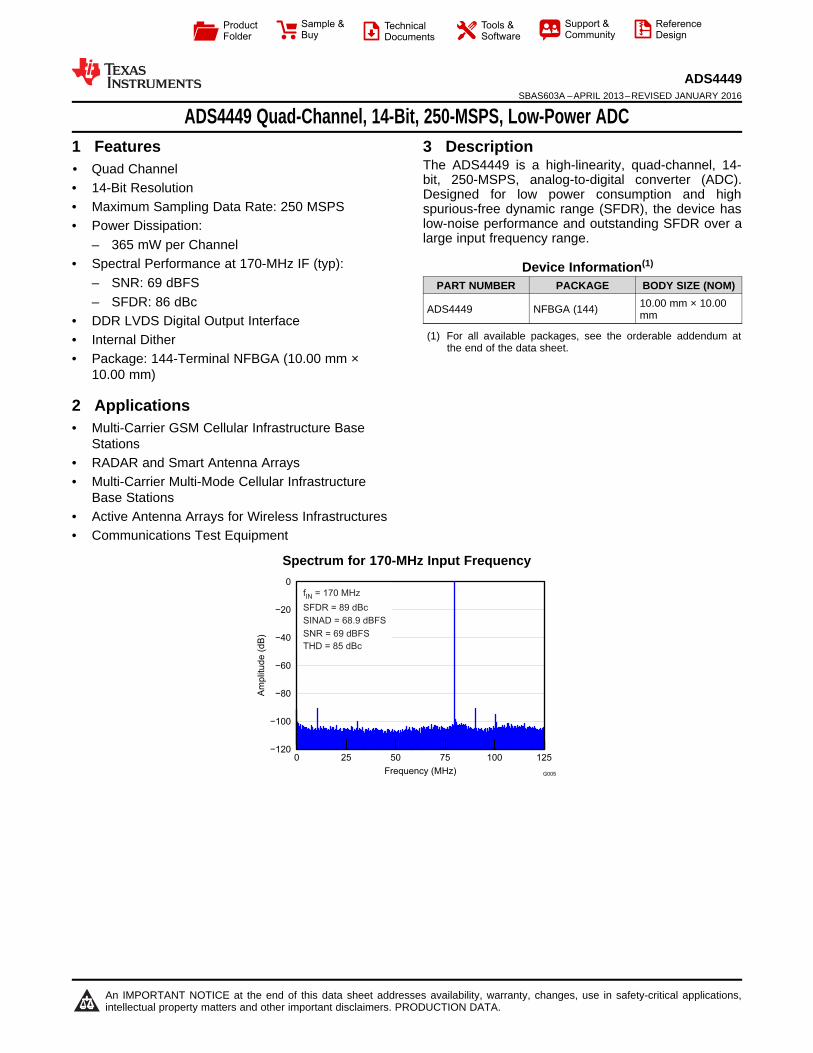
-120 -100 -80 -60 -40 -20 0 0 25 50 75 100 125 Frequency (MHz) Amplitude (dB) G005 f = 170 MHz IN SFDR = 89 dBc SNR = 69 dBFS SINAD = 68.9 dBFS THD = 85 dBc Product Folder Sample & Buy Technical Documents Tools & Software Support & Community Reference Design An IMPORTANT NOTICE at the end of this data sheet addresses availability, warranty, changes, use in safety-critical applications, intellectual property matters and other important disclaimers. PRODUCTION DATA. ADS4449 SBAS603A – APRIL 2013 – REVISED JANUARY 2016 ADS4449 Quad-Channel, 14-Bit, 250-MSPS, Low-Power ADC 1 1 Features 1• Quad Channel • 14-Bit Resolution • Maximum Sampling Data Rate: 250 MSPS • Power Dissipation: – 365 mW per Channel • Spectral Performance at 170-MHz IF (typ): – SNR: 69 dBFS – SFDR: 86 dBc • DDR LVDS Digital Output Interface • Internal Dither • Package: 144-Terminal NFBGA (10.00 mm × 10.00 mm) 2 Applications • Multi-Carrier GSM Cellular Infrastructure Base Stations • RADAR and Smart Antenna Arrays • Multi-Carrier Multi-Mode Cellular Infrastructure Base Stations • Active Antenna Arrays for Wireless Infrastructures • Communications Test Equipment 3 Description The ADS4449 is a high-linearity, quad-channel, 14- bit, 250-MSPS, analog-to-digital converter (ADC). Designed for low power consumption and high spurious-free dynamic range (SFDR), the device has low-noise performance and outstanding SFDR over a large input frequency range. Device Information (1) PART NUMBER PACKAGE BODY SIZE (NOM) ADS4449 NFBGA (144) 10.00 mm × 10.00 mm (1) For all available packages, see the orderable addendum at the end of the data sheet. Spectrum for 170-MHz Input Frequency
Transcript of ADS4449 Quad-Channel, 14-Bit, 250-MSPS, Low-Power … · !120!100!80!60!40!20 0 0 25 50 75 100 125...
−120
−100
−80
−60
−40
−20
0
0 25 50 75 100 125
Frequency (MHz)
Am
plit
ude (
dB
)
G005
f = 170 MHzIN
SFDR = 89 dBc
SNR = 69 dBFS
SINAD = 68.9 dBFS
THD = 85 dBc
Product
Folder
Sample &Buy
Technical
Documents
Tools &
Software
Support &Community
ReferenceDesign
An IMPORTANT NOTICE at the end of this data sheet addresses availability, warranty, changes, use in safety-critical applications,intellectual property matters and other important disclaimers. PRODUCTION DATA.
ADS4449SBAS603A –APRIL 2013–REVISED JANUARY 2016
ADS4449 Quad-Channel, 14-Bit, 250-MSPS, Low-Power ADC
1
1 Features1• Quad Channel• 14-Bit Resolution• Maximum Sampling Data Rate: 250 MSPS• Power Dissipation:
– 365 mW per Channel• Spectral Performance at 170-MHz IF (typ):
– SNR: 69 dBFS– SFDR: 86 dBc
• DDR LVDS Digital Output Interface• Internal Dither• Package: 144-Terminal NFBGA (10.00 mm ×
10.00 mm)
2 Applications• Multi-Carrier GSM Cellular Infrastructure Base
Stations• RADAR and Smart Antenna Arrays• Multi-Carrier Multi-Mode Cellular Infrastructure
Base Stations• Active Antenna Arrays for Wireless Infrastructures• Communications Test Equipment
3 DescriptionThe ADS4449 is a high-linearity, quad-channel, 14-bit, 250-MSPS, analog-to-digital converter (ADC).Designed for low power consumption and highspurious-free dynamic range (SFDR), the device haslow-noise performance and outstanding SFDR over alarge input frequency range.
Device Information(1)
PART NUMBER PACKAGE BODY SIZE (NOM)
ADS4449 NFBGA (144) 10.00 mm × 10.00mm
(1) For all available packages, see the orderable addendum atthe end of the data sheet.
Spectrum for 170-MHz Input Frequency
2
ADS4449SBAS603A –APRIL 2013–REVISED JANUARY 2016 www.ti.com
Product Folder Links: ADS4449
Submit Documentation Feedback Copyright © 2013–2016, Texas Instruments Incorporated
Table of Contents1 Features .................................................................. 12 Applications ........................................................... 13 Description ............................................................. 14 Revision History..................................................... 25 Pin Configuration and Functions ......................... 36 Specifications......................................................... 5
6.1 Absolute Maximum Ratings ...................................... 56.2 ESD Ratings.............................................................. 56.3 Recommended Operating Conditions....................... 56.4 Thermal Information .................................................. 66.5 Electrical Characteristics........................................... 76.6 Digital Characteristics ............................................... 96.7 Timing Requirements .............................................. 106.8 Timing Characteristics For Figure 1........................ 106.9 Typical Characteristics ............................................ 126.10 Typical Characteristics: Contour ........................... 18
7 Parameter Measurement Information ................ 197.1 LVDS Output Timing ............................................... 19
8 Detailed Description ............................................ 218.1 Overview ................................................................. 21
8.2 Functional Block Diagram ....................................... 218.3 Feature Description................................................. 228.4 Device Functional Modes........................................ 238.5 Programming .......................................................... 268.6 Register Maps ........................................................ 28
9 Application and Implementation ........................ 419.1 Application Information............................................ 419.2 Typical Application .................................................. 41
10 Power Supply Recommendations ..................... 4811 Layout................................................................... 48
11.1 Layout Guidelines ................................................. 4811.2 Layout Example ................................................... 48
12 Device and Documentation Support ................. 4912.1 Device Nomenclature............................................ 4912.2 Documentation Support ........................................ 5012.3 Community Resources.......................................... 5012.4 Trademarks ........................................................... 5012.5 Electrostatic Discharge Caution............................ 5012.6 Glossary ................................................................ 50
13 Mechanical, Packaging, and OrderableInformation ........................................................... 50
4 Revision HistoryNOTE: Page numbers for previous revisions may differ from page numbers in the current version.
Changes from Original (April 2013) to Revision A Page
• Added Internal Dither Features bullet .................................................................................................................................... 1• Added ESD Ratings table, Feature Description section, Device Functional Modes section, Application and
Implementation section, Power Supply Recommendations section, Layout section, Device and DocumentationSupport section, and Mechanical, Packaging, and Orderable Information section................................................................ 1
• Deleted Package and Ordering Information because the data is repeated in the Package Option Addendum ................... 1• Deleted SNRB from the configuration registers block in the functional block diagram ......................................................... 1• Changed Clock Inputs, Input clock sample rate parameter minimum specification in Recommended Operating
Conditions table ...................................................................................................................................................................... 5• Changed Table 2 ................................................................................................................................................................. 22
A
B
C
D
E
F
G
H
J
1 2 3 4 5 6 7 8 9 10 11 12
K
L
M
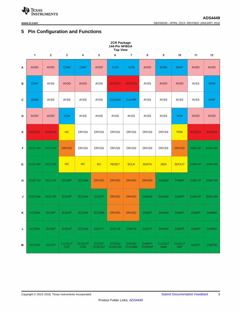
CINPAVDD AVDD CINM AVDD VCM VCM AVDD BINM AVDD AVDD
DINP AVSS AVDD AVDD AVSS AVDD33 AVDD33 AVSS AVDD AVDD AVSS AINM
DINM AVSS AVSS AVSS CLKINM CLKINP AVSS AVSS AVSS AVSS AINP
AVDD AVDD VCM AVSS AVSS AVSS AVSS AVSS AVSS VCM AVDD AVDD
AVDD33 AVDD33 NC DRVSS AVDD33 AVDD33
DCD13M DCD13P DRVDD DRVSS DAB13P DAB13M
DCD12M DCD12P NC NC DAB12P
DCD11M DCD11P DCD6P DCD6M DAB11P DAB11M
DCD10M DCD10P DCD5P DCD5M DAB10P DAB10M
DCD9M DCD9P DCD4P DCD4M DAB9P DAB9M
DCD8M DCD8P DCD3P DCD3M DCD1P DCD1M DAB1M DAB1P DAB3M DAB3P DAB8P DAB8M
DCD7M DCD7PCLKOUT
CDP
CLKOUT
CDM
DCD0P/
OVRCDP
DCD0M/
OVRCDM
DAB0M/
OVRABM
DAB0P/
OVRABP
CLKOUT
ABM
CLKOUT
ABPDAB7P DAB7M
DRVSSDRVSS
SDATA
DRVDD
DAB2M
DAB2P DAB4M DAB4P
DAB5P
DAB6P
SDOUT
DRVDD
PDNDRVSSDRVSS
DRVDD
DRVDD
DRVDD
SCLK
DRVSS
DRVSS
DRVDD
DRVDD
DRVDD
RESET
DRVSS
DRVSS
DCD2M
DCD2P
DRVDD
NC
DRVSS
DRVSS
AVSS
DAB12M
DAB5M
DAB6M
SEN
BINP
3
ADS4449www.ti.com SBAS603A –APRIL 2013–REVISED JANUARY 2016
Product Folder Links: ADS4449
Submit Documentation FeedbackCopyright © 2013–2016, Texas Instruments Incorporated
5 Pin Configuration and Functions
ZCR Package144-Pin NFBGA
Top View
4
ADS4449SBAS603A –APRIL 2013–REVISED JANUARY 2016 www.ti.com
Product Folder Links: ADS4449
Submit Documentation Feedback Copyright © 2013–2016, Texas Instruments Incorporated
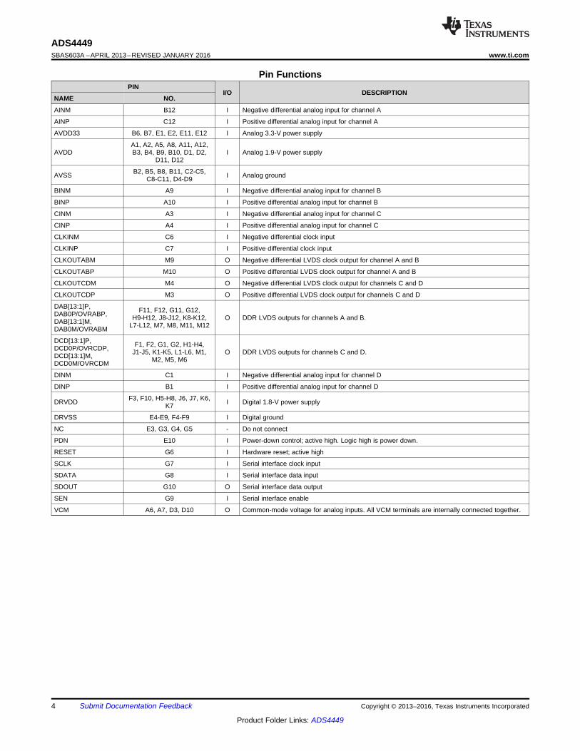
Pin FunctionsPIN
I/O DESCRIPTIONNAME NO.
AINM B12 I Negative differential analog input for channel A
AINP C12 I Positive differential analog input for channel A
AVDD33 B6, B7, E1, E2, E11, E12 I Analog 3.3-V power supply
AVDDA1, A2, A5, A8, A11, A12,B3, B4, B9, B10, D1, D2,
D11, D12I Analog 1.9-V power supply
AVSS B2, B5, B8, B11, C2-C5,C8-C11, D4-D9 I Analog ground
BINM A9 I Negative differential analog input for channel B
BINP A10 I Positive differential analog input for channel B
CINM A3 I Negative differential analog input for channel C
CINP A4 I Positive differential analog input for channel C
CLKINM C6 I Negative differential clock input
CLKINP C7 I Positive differential clock input
CLKOUTABM M9 O Negative differential LVDS clock output for channel A and B
CLKOUTABP M10 O Positive differential LVDS clock output for channel A and B
CLKOUTCDM M4 O Negative differential LVDS clock output for channels C and D
CLKOUTCDP M3 O Positive differential LVDS clock output for channels C and D
DAB[13:1]P,DAB0P/OVRABP,DAB[13:1]M,DAB0M/OVRABM
F11, F12, G11, G12,H9-H12, J8-J12, K8-K12,
L7-L12, M7, M8, M11, M12O DDR LVDS outputs for channels A and B.
DCD[13:1]P,DCD0P/OVRCDP,DCD[13:1]M,DCD0M/OVRCDM
F1, F2, G1, G2, H1-H4,J1-J5, K1-K5, L1-L6, M1,
M2, M5, M6O DDR LVDS outputs for channels C and D.
DINM C1 I Negative differential analog input for channel D
DINP B1 I Positive differential analog input for channel D
DRVDD F3, F10, H5-H8, J6, J7, K6,K7 I Digital 1.8-V power supply
DRVSS E4-E9, F4-F9 I Digital ground
NC E3, G3, G4, G5 - Do not connect
PDN E10 I Power-down control; active high. Logic high is power down.
RESET G6 I Hardware reset; active high
SCLK G7 I Serial interface clock input
SDATA G8 I Serial interface data input
SDOUT G10 O Serial interface data output
SEN G9 I Serial interface enable
VCM A6, A7, D3, D10 O Common-mode voltage for analog inputs. All VCM terminals are internally connected together.
5
ADS4449www.ti.com SBAS603A –APRIL 2013–REVISED JANUARY 2016
Product Folder Links: ADS4449
Submit Documentation FeedbackCopyright © 2013–2016, Texas Instruments Incorporated
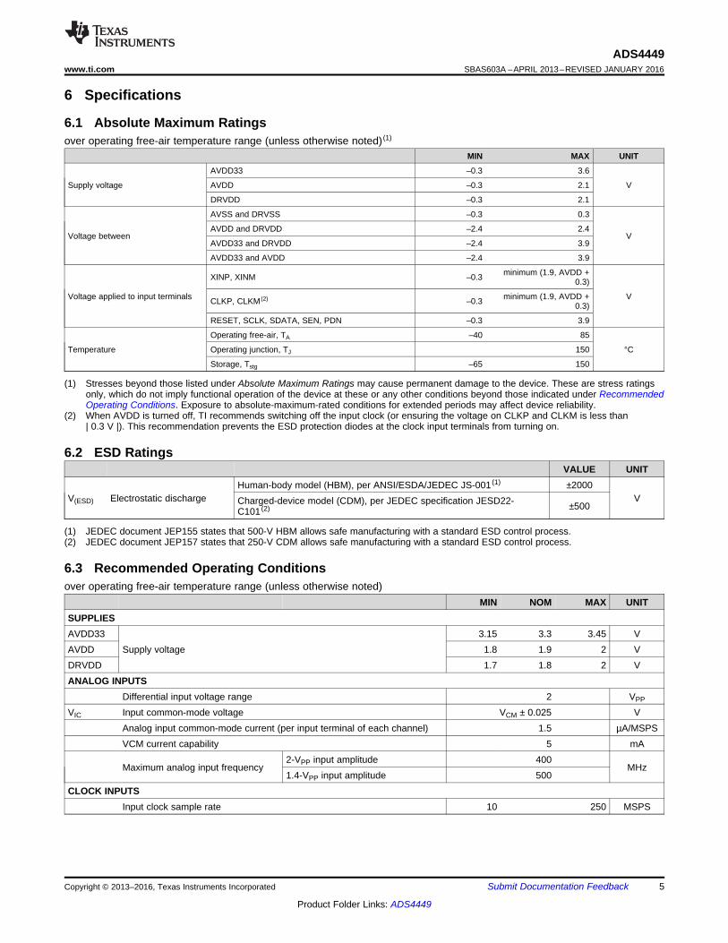
(1) Stresses beyond those listed under Absolute Maximum Ratings may cause permanent damage to the device. These are stress ratingsonly, which do not imply functional operation of the device at these or any other conditions beyond those indicated under RecommendedOperating Conditions. Exposure to absolute-maximum-rated conditions for extended periods may affect device reliability.
(2) When AVDD is turned off, TI recommends switching off the input clock (or ensuring the voltage on CLKP and CLKM is less than| 0.3 V |). This recommendation prevents the ESD protection diodes at the clock input terminals from turning on.
6 Specifications
6.1 Absolute Maximum Ratingsover operating free-air temperature range (unless otherwise noted) (1)
MIN MAX UNIT
Supply voltage
AVDD33 –0.3 3.6
VAVDD –0.3 2.1
DRVDD –0.3 2.1
Voltage between
AVSS and DRVSS –0.3 0.3
VAVDD and DRVDD –2.4 2.4
AVDD33 and DRVDD –2.4 3.9
AVDD33 and AVDD –2.4 3.9
Voltage applied to input terminals
XINP, XINM –0.3 minimum (1.9, AVDD +0.3)
VCLKP, CLKM (2) –0.3 minimum (1.9, AVDD +0.3)
RESET, SCLK, SDATA, SEN, PDN –0.3 3.9
Temperature
Operating free-air, TA –40 85
°COperating junction, TJ 150
Storage, Tstg –65 150
(1) JEDEC document JEP155 states that 500-V HBM allows safe manufacturing with a standard ESD control process.(2) JEDEC document JEP157 states that 250-V CDM allows safe manufacturing with a standard ESD control process.
6.2 ESD RatingsVALUE UNIT
V(ESD) Electrostatic dischargeHuman-body model (HBM), per ANSI/ESDA/JEDEC JS-001 (1) ±2000
VCharged-device model (CDM), per JEDEC specification JESD22-C101 (2) ±500
6.3 Recommended Operating Conditionsover operating free-air temperature range (unless otherwise noted)
MIN NOM MAX UNITSUPPLIESAVDD33
Supply voltage3.15 3.3 3.45 V
AVDD 1.8 1.9 2 VDRVDD 1.7 1.8 2 VANALOG INPUTS
Differential input voltage range 2 VPP
VIC Input common-mode voltage VCM ± 0.025 VAnalog input common-mode current (per input terminal of each channel) 1.5 µA/MSPSVCM current capability 5 mA
Maximum analog input frequency2-VPP input amplitude 400
MHz1.4-VPP input amplitude 500
CLOCK INPUTSInput clock sample rate 10 250 MSPS

6
ADS4449SBAS603A –APRIL 2013–REVISED JANUARY 2016 www.ti.com
Product Folder Links: ADS4449
Submit Documentation Feedback Copyright © 2013–2016, Texas Instruments Incorporated
Recommended Operating Conditions (continued)over operating free-air temperature range (unless otherwise noted)
MIN NOM MAX UNIT
(1) Prolonged use at this junction temperature may increase the device failure-in-time (FIT) rate.
Input clock amplitude differential(VCLKP – VCLKM)
Sine wave, ac-coupled 0.2 1.5
VPPLVPECL, ac-coupled 1.6LVDS, ac-coupled 0.7LVCMOS, single-ended, ac-coupled 1.8
Input clock duty cycle 40% 50% 60%DIGITAL OUTPUTS
CLOADMaximum external load capacitance from each output terminal to DRVSS(default strength) 3.3 pF
RLOAD Differential load resistance between the LVDS output pairs (LVDS mode) 100 ΩTEMPERATURE RANGETA Operating free-air temperature –40 85 °C
TJ Operating junction temperatureRecommended 105
°CMaximum rated (1) 125
(1) For more information about traditional and new thermal metrics, see the Semiconductor and IC Package Thermal Metrics applicationreport, SPRA953.
6.4 Thermal Information
THERMAL METRIC (1)ADS4449
UNITZCR (NFBGA)144 PINS
RθJA Junction-to-ambient thermal resistance 35.9 °C/WRθJC(top) Junction-to-case (top) thermal resistance 5.1 °C/WRθJB Junction-to-board thermal resistance 12.6 °C/WψJT Junction-to-top characterization parameter 0.1 °C/WψJB Junction-to-board characterization parameter 12.4 °C/WRθJC(bot) Junction-to-case (bottom) thermal resistance N/A °C/W

7
ADS4449www.ti.com SBAS603A –APRIL 2013–REVISED JANUARY 2016
Product Folder Links: ADS4449
Submit Documentation FeedbackCopyright © 2013–2016, Texas Instruments Incorporated
(1) There are two sources of gain error: internal reference inaccuracy and channel gain error.(2) A 185-MHz, full-scale, sine-wave input signal is applied to all four channels.
6.5 Electrical CharacteristicsTypical values are at TA = 25°C, full temperature range is TMIN = –40°C to TMAX = 85°C, ADC clock frequency = 250 MHz,50% clock duty cycle, AVDD33V = 3.3 V, AVDD = 1.9 V, DRVDD = 1.8 V, and –1-dBFS differential input, unless otherwisenoted.
PARAMETER TEST CONDITIONS MIN TYP MAX UNITS
RESOLUTION
Default resolution 14 Bits
ANALOG INPUTS
Differential input full-scale 2 VPP
VCM Common mode input voltage 1.15 V
RIN Input resistance, differential At 170-MHz input frequency 700 Ω
CIN Input capacitance, differential At 170-MHz input frequency 3.3 pF
Analog input bandwidth, 3 dB with a 50-Ω source driving the ADC analoginputs 500 MHz
DYNAMIC ACCURACY
EO Offset error Specified across devices and channels –15 15 mV
EG Gain error (1)
As a result of internalreference inaccuracyalone
Specified across devices and channels –5 5%FS
Of channel alone Specified across channels within a device ±0.2
Channel gain error temperature coefficient (1) 0.001 Δ%/°C
POWER SUPPLY (2)
IAVDD33
Supply current
3.3-V analog supply 51 mA
IAVDD 1.9-V analog supply 350 mA
IDRVDD 1.8-V digital supply 355 mA
PTOTAL
Power dissipation
Total 1.47 1.6 W
PDISS(standby) Standby 400 mW
PDISS(global) Global power-down 6 52 mW
DYNAMIC AC CHARACTERISTICS
SNR Signal-to-noise ratio
fIN = 40 MHz 71.1
dBFS
fIN = 70 MHz 71
fIN = 140 MHz 69.5
fIN = 170 MHz 67.5 69
fIN = 220 MHz 68.5
fIN = 307 MHz 67.5
fIN = 350 MHz 67
SINAD Signal-to-noise and distortion ratio
fIN = 40 MHz 70.9
dBFS
fIN = 70 MHz 70.8
fIN = 140 MHz 69.3
fIN = 170 MHz 66.9 68.8
fIN = 220 MHz 68.3
fIN = 307 MHz 66.8
fIN = 350 MHz 66.3
SFDR Spurious-free dynamic range
fIN = 40 MHz 84
dBc
fIN = 70 MHz 87
fIN = 140 MHz 85
fIN = 170 MHz 78.5 86
fIN = 220 MHz 84
fIN = 307 MHz 78
fIN = 350 MHz 77

8
ADS4449SBAS603A –APRIL 2013–REVISED JANUARY 2016 www.ti.com
Product Folder Links: ADS4449
Submit Documentation Feedback Copyright © 2013–2016, Texas Instruments Incorporated
Electrical Characteristics (continued)Typical values are at TA = 25°C, full temperature range is TMIN = –40°C to TMAX = 85°C, ADC clock frequency = 250 MHz,50% clock duty cycle, AVDD33V = 3.3 V, AVDD = 1.9 V, DRVDD = 1.8 V, and –1-dBFS differential input, unless otherwisenoted.
PARAMETER TEST CONDITIONS MIN TYP MAX UNITS
(3) Phase and amplitude imbalances onboard must be minimized to obtain good performance.(4) The minimum value across temperature is ensured by bench characterization.
THD Total harmonic distortion
fIN = 40 MHz 83
dBc
fIN = 70 MHz 84
fIN = 140 MHz 82
fIN = 170 MHz 75 83
fIN = 220 MHz 82
fIN = 307 MHz 76
fIN = 350 MHz 75
HD2 Second-order harmonic distortion (3) (4)
fIN = 40 MHz 96
dBc
fIN = 70 MHz 87
fIN = 140 MHz 86
fIN = 170 MHz 78.5 86
fIN = 220 MHz 84
fIN = 307 MHz 78
fIN = 350 MHz 77
HD3 Third-order harmonic distortion
fIN = 40 MHz 83
dBc
fIN = 70 MHz 89
fIN = 140 MHz 85
fIN = 170 MHz 79.5 86
fIN = 220 MHz 85
fIN = 307 MHz 80
fIN = 350 MHz 78
Worst spur(non HD2, HD3)
fIN = 40 MHz 100
dBc
fIN = 70 MHz 100
fIN = 140 MHz 95
fIN = 170 MHz 87 95
fIN = 220 MHz, 95
fIN = 307 MHz 85
fIN = 350 MHz 85
DNL Differential nonlinearity –0.95 ±0.5 LSBs
INL Integral nonlinearity ±1.5 ±5.25 LSBs
Input overload recovery Recovery to within 1% (of final value) for6-dB output overload with sine-wave input 1 Clock
cycle
Crosstalkwith a full-scale, 220-MHz signal onaggressor channel and no signal on victimchannel
90 dB
PSRR AC power-supply rejection ratio For 50-mVPP signal on AVDD supply < 30 dB
9
ADS4449www.ti.com SBAS603A –APRIL 2013–REVISED JANUARY 2016
Product Folder Links: ADS4449
Submit Documentation FeedbackCopyright © 2013–2016, Texas Instruments Incorporated
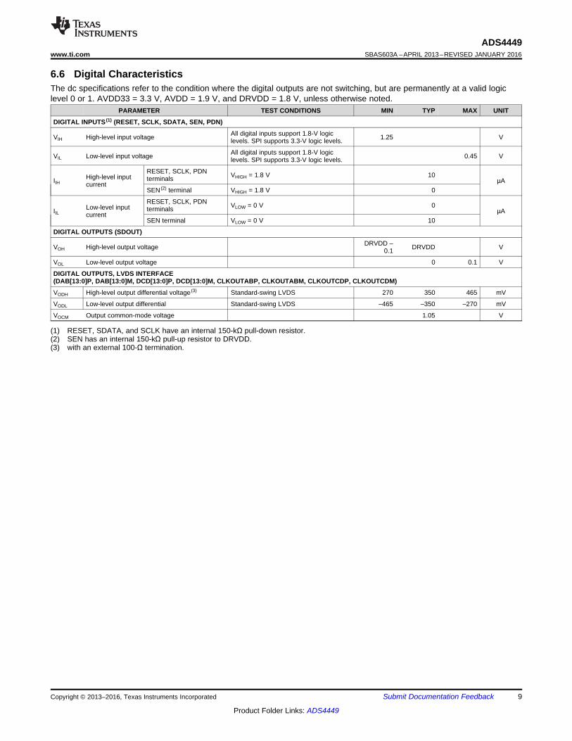
(1) RESET, SDATA, and SCLK have an internal 150-kΩ pull-down resistor.(2) SEN has an internal 150-kΩ pull-up resistor to DRVDD.(3) with an external 100-Ω termination.
6.6 Digital CharacteristicsThe dc specifications refer to the condition where the digital outputs are not switching, but are permanently at a valid logiclevel 0 or 1. AVDD33 = 3.3 V, AVDD = 1.9 V, and DRVDD = 1.8 V, unless otherwise noted.
PARAMETER TEST CONDITIONS MIN TYP MAX UNIT
DIGITAL INPUTS (1) (RESET, SCLK, SDATA, SEN, PDN)
VIH High-level input voltage All digital inputs support 1.8-V logiclevels. SPI supports 3.3-V logic levels. 1.25 V
VIL Low-level input voltage All digital inputs support 1.8-V logiclevels. SPI supports 3.3-V logic levels. 0.45 V
IIHHigh-level inputcurrent
RESET, SCLK, PDNterminals VHIGH = 1.8 V 10
µASEN (2) terminal VHIGH = 1.8 V 0
IILLow-level inputcurrent
RESET, SCLK, PDNterminals VLOW = 0 V 0
µASEN terminal VLOW = 0 V 10
DIGITAL OUTPUTS (SDOUT)
VOH High-level output voltage DRVDD –0.1 DRVDD V
VOL Low-level output voltage 0 0.1 V
DIGITAL OUTPUTS, LVDS INTERFACE(DAB[13:0]P, DAB[13:0]M, DCD[13:0]P, DCD[13:0]M, CLKOUTABP, CLKOUTABM, CLKOUTCDP, CLKOUTCDM)
VODH High-level output differential voltage (3) Standard-swing LVDS 270 350 465 mV
VODL Low-level output differential Standard-swing LVDS –465 –350 –270 mV
VOCM Output common-mode voltage 1.05 V
10
ADS4449SBAS603A –APRIL 2013–REVISED JANUARY 2016 www.ti.com
Product Folder Links: ADS4449
Submit Documentation Feedback Copyright © 2013–2016, Texas Instruments Incorporated
(1) Timing parameters are ensured by design and characterization and are not tested in production.(2) CLOAD is the effective external single-ended load capacitance between each output terminal and ground.(3) RLOAD is the differential load resistance between the LVDS output pair.(4) ADC latency is given for channels B and D. For channels A and C, latency reduces by half of the output clock cycles.(5) Overall latency = ADC latency + tPDI.(6) Measurements are done with a transmission line of 100-Ω characteristic impedance between the device and load. Setup and hold time
specifications take into account the effect of jitter on the output data and clock.(7) Data valid refers to a logic high of 100 mV and a logic low of –100 mV.(8) Note that these numbers are taken with delayed output clocks by writing the following registers: address A9h, value 02h; and address
ACh, value 60h. Refer to the section. By default after reset, minimum setup time and minimum hold times are 520 ps each.(9) The setup and hold times of a channel are measured with respect to the same channel output clock.
6.7 Timing Requirements (1)
Typical values are at 25°C, AVDD33 = 3.3 V, AVDD = 1.9 V, DRVDD = 1.8 V, sine-wave input clock, CLOAD = 3.3 pF (2), andRLOAD = 100 Ω (3), unless otherwise noted.Minimum and maximum values are across the full temperature range of TMIN = –40°C to TMAX = 85°C.
MIN NOM MAX UNIT
tA Aperture delay 0.7 1.2 1.6 ns
Aperture delay matching Between any two channels of the same device ±70 ps
Variation of aperture delay Between two devices at the same temperature andDRVDD supply ±150 ps
tJ Aperture jitter 140 fs rms
Wake up time
Time to valid data after coming out of global powerdown 100
µsTime to valid data after coming out of channel powerdown 10
ADC latency (4) (5)
Default latency in 14-bit mode 10Output clock
cyclesDigital gain enabled 13
Digital gain and offset correction enabled 14
OUTPUT TIMING (6)
tSU Data setup time (7) (8) (9) Data valid to CLKOUTxxP zero-crossing 0.6 0.85 ns
tH Data hold time (7) (8) (9) CLKOUTxxP zero-crossing to data becoming invalid 0.6 0.84 ns
LVDS bit clock duty cycle Differential clock duty cycle (CLKOUTxxP –CLKOUTxxM) 50%
tPDI Clock propagation delay (5)Input clock falling edge cross-over to output clockfalling edge cross-over, 184 MSPS ≤ samplingfrequency ≤ 250 MSPS
0.25 × tS + tdelay ns
tdelay Delay timeInput clock falling edge cross-over to output clockfalling edge cross-over, 184 MSPS ≤ samplingfrequency ≤ 250 MSPS
6.9 8.65 10.5 ns
tRISE,tFALL
Data rise and fall time Rise time measured from –100 mV to 100 mV 0.1 ns
tCLKRISE,tCLKFALL
Output clock rise and falltime Rise time measured from –100 mV to 100 mV 0.1 ns
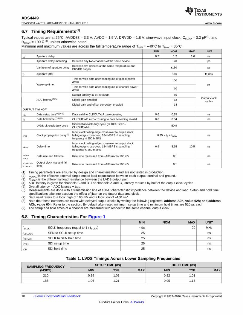
6.8 Timing Characteristics For Figure 1MIN NOM MAX UNIT
fSCLK SCLK frequency (equal to 1 / tSCLK) > dc 20 MHztSLOADS SEN to SCLK setup time 25 nstSLOADH SCLK to SEN hold time 25 nstDSU SDI setup time 25 nstDH SDI hold time 25 ns
Table 1. LVDS Timings Across Lower Sampling Frequencies
SAMPLING FREQUENCY(MSPS)
SETUP TIME (ns) HOLD TIME (ns)MIN TYP MAX MIN TYP MAX
210 0.89 1.03 0.82 1.01185 1.06 1.21 0.95 1.15
A7 A6 A5 A4 A3 A2 A1 A0 D7 D6 D5 D4 D3 D2 D1 D0SDATA
SCLK
tSCLK tDSU
tDH
SEN
tSLOADS tSLOADH
RESET
Register Address Register Data
11
ADS4449www.ti.com SBAS603A –APRIL 2013–REVISED JANUARY 2016
Product Folder Links: ADS4449
Submit Documentation FeedbackCopyright © 2013–2016, Texas Instruments Incorporated
Figure 1. Serial Interface Timing

−120
−100
−80
−60
−40
−20
0
0 25 50 75 100 125Frequency (MHz)
Am
plitu
de (
dB)
G005
−120
−100
−80
−60
−40
−20
0
0 25 50 75 100 125Frequency (MHz)
Am
plitu
de (
dB)
G006
−120
−100
−80
−60
−40
−20
0
0 25 50 75 100 125Frequency (MHz)
Am
plitu
de (
dBF
S)
G003
−120
−100
−80
−60
−40
−20
0
0 25 50 75 100 125Frequency (MHz)
Am
plitu
de (
dB)
G004
−120
−100
−80
−60
−40
−20
0
0 25 50 75 100 125Frequency (MHz)
Am
plitu
de (
dBF
S)
G001
−120
−100
−80
−60
−40
−20
0
0 25 50 75 100 125Frequency (MHz)
Am
plitu
de (
dBF
S)
G002
12
ADS4449SBAS603A –APRIL 2013–REVISED JANUARY 2016 www.ti.com
Product Folder Links: ADS4449
Submit Documentation Feedback Copyright © 2013–2016, Texas Instruments Incorporated
6.9 Typical CharacteristicsAt 25°C, AVDD = 1.9 V, AVDD3V = 3.3 V, DRVDD = 1.8 V, rated sampling frequency, 0-dB gain, sine-wave input clock,1.5-VPP differential clock amplitude, 50% clock duty cycle, –1-dBFS differential analog input, DDR LVDS output interface, and32k-point FFT, unless otherwise noted.
fIN = 40 MHz SFDR = 84 dBc SNR = 71.1 dBFSSINAD = 70.9 dBFS THD = 84 dBc
Figure 2. FFT for 40-MHz Input Signal
fIN = 70 MHz SFDR = 87 dBc SNR = 70.9 dBFSSINAD = 70.8 dBFS THD = 84 dBc
Figure 3. FFT for 70-MHz Input Signal
fIN = 100 MHz SFDR = 85 dBc SNR = 70.2 dBFSSINAD = 70.1 dBFS THD = 84 dBc
Figure 4. FFT for 100-MHz Input Signal
fIN = 140 MHz SFDR = 87 dBc SNR = 69.7 dBFSSINAD = 69.6 dBFS THD = 84 dBc
Figure 5. FFT for 140-MHz Input Signal
fIN = 170 MHz SFDR = 89 dBc SNR = 69 dBFSSINAD = 68.9 dBFS THD = 85 dBc
Figure 6. FFT for 170-MHz Input Signal
fIN = 230 MHz SFDR = 86 dBc SNR = 68.9 dBFSSINAD = 68.5 dBFS THD = 84 dBc
Figure 7. FFT for 230-MHz Input Signal
70
73
76
79
82
85
88
91
93
40 80 120 160 200 240 280 320 360 400Input Frequency (MHz)
SF
DR
(dB
c)
G011
−10
8−
105
−10
4−
103
−10
2−
101
−10
0−
99−
98−
97−
96−
95−
94−
93−
92−
91−
90−
89−
88−
87−
86−
85−
84−
83−
82
−10
8−
105
−10
4−
103
−10
2−
101
−10
0−
99−
98−
97−
96−
95−
94−
93−
92−
91−
90−
89−
88−
87−
86−
85−
84−
83−
82
0
5
10
15
20
25
HD2 (dBc)
Cou
nt (
%)
Temperature = −40°CTemperature = 25°CTemperature = 85°C
G039
−120
−100
−80
−60
−40
−20
0
0 25 50 75 100 125Frequency (MHz)
Am
plitu
de (
dB)
G009
−120
−100
−80
−60
−40
−20
0
0 25 50 75 100 125Frequency (MHz)
Am
plitu
de (
dB)
G010
−120
−100
−80
−60
−40
−20
0
0 25 50 75 100 125Frequency (MHz)
Am
plitu
de (
dBF
S)
G007
−120
−100
−80
−60
−40
−20
0
0 25 50 75 100 125Frequency (MHz)
Am
plitu
de (
dBF
S)
G008
13
ADS4449www.ti.com SBAS603A –APRIL 2013–REVISED JANUARY 2016
Product Folder Links: ADS4449
Submit Documentation FeedbackCopyright © 2013–2016, Texas Instruments Incorporated
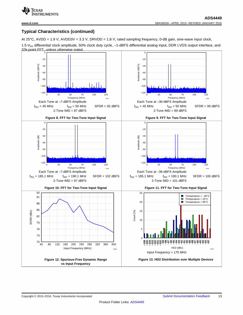
Typical Characteristics (continued)At 25°C, AVDD = 1.9 V, AVDD3V = 3.3 V, DRVDD = 1.8 V, rated sampling frequency, 0-dB gain, sine-wave input clock,
1.5-VPP differential clock amplitude, 50% clock duty cycle, –1-dBFS differential analog input, DDR LVDS output interface, and32k-point FFT, unless otherwise noted.
Each Tone at –7-dBFS AmplitudefIN1 = 45 MHz fIN2 = 50 MHz SFDR = 92 dBFS
2-Tone IMD = 87 dBFS
Figure 8. FFT for Two-Tone Input Signal
Each Tone at –36-dBFS AmplitudefIN1 = 45 MHz fIN2 = 50 MHz SFDR = 99 dBFS
2-Tone IMD = 99 dBFS
Figure 9. FFT for Two-Tone Input Signal
Each Tone at –7-dBFS AmplitudefIN1 = 185.1 MHz fIN2 = 190.1 MHz SFDR = 102 dBFS
2-Tone IMD = 97 dBFS
Figure 10. FFT for Two-Tone Input Signal
Each Tone at –36-dBFS AmplitudefIN1 = 185.1 MHz fIN2 = 190.1 MHz SFDR = 100 dBFS
2-Tone IMD = 101 dBFS
Figure 11. FFT for Two-Tone Input Signal
Figure 12. Spurious-Free Dynamic Rangevs Input Frequency
Input Frequency = 170 MHz
Figure 13. HD2 Distribution over Multiple Devices

−50 −40 −30 −20 −10 020
30
40
50
60
70
80
90
100
110
120
69
69.5
70
70.5
71
71.5
72
72.5
73
73.5
74
Amplitude (dBFS)
SF
DR
(dB
c,dB
FS
)
SN
R (
dBF
S)
SFDR (dBc)SFDR (dBFS)SNR
G016
0.7 0.8 0.9 1 1.1 1.2 1.378
80
82
84
86
88
90
92
94
68
68.5
69
69.5
70
70.5
71
71.5
72
Input Common−Mode Voltage (V)
SF
DR
(dB
c)
SN
R (
dBF
S)
SFDRSNR
G017
62
63
64
65
66
67
68
69
70
71
72
73
74
0 0.5 1 1.5 2 2.5 3 3.5 4 4.5 5 5.5 6Digital Gain (dB)
SN
R (
dBF
S)
40 MHz100 MHz130 MHz
170 MHz230 MHz300 MHz
350 MHz400 MHz450 MHz
G014
−70 −60 −50 −40 −30 −20 −10 070
70.5
71
71.5
72
72.5
73
73.5
74
74.5
75
75.5
20
30
40
50
60
70
80
90
100
110
120
130
Amplitude (dBFS)
SN
R (
dBF
S)
SF
DR
(dB
c,dB
FS
)
SNR(dBFS)SFDR(dBc)SFDR(dBFS)
G015
65
66
67
68
69
70
71
72
40 80 120 160 200 240 280 320 360 400Input Frequency (MHz)
SN
R (
dBF
S)
G012
64
68
72
76
80
84
88
92
96
100
104
0 0.5 1 1.5 2 2.5 3 3.5 4 4.5 5 5.5 6Digital Gain (dB)
SF
DR
(dB
c)
40 MHz100 MHz130 MHz
170 MHz230 MHz300 MHz
350 MHz400 MHz450 MHz
G013
14
ADS4449SBAS603A –APRIL 2013–REVISED JANUARY 2016 www.ti.com
Product Folder Links: ADS4449
Submit Documentation Feedback Copyright © 2013–2016, Texas Instruments Incorporated
Typical Characteristics (continued)At 25°C, AVDD = 1.9 V, AVDD3V = 3.3 V, DRVDD = 1.8 V, rated sampling frequency, 0-dB gain, sine-wave input clock,
1.5-VPP differential clock amplitude, 50% clock duty cycle, –1-dBFS differential analog input, DDR LVDS output interface, and32k-point FFT, unless otherwise noted.
Figure 14. Signal-to-Noise Ratio vs Input Frequency Figure 15. Spurious-Free Dynamic Rangevs Digital Gain
Figure 16. Signal-to-Noise Ratio vs Digital Gain
Input Frequency = 70 MHz
Figure 17. Performance vs Input Amplitude
Input Frequency = 185 MHz
Figure 18. Performance vs Input Amplitude
Input Frequency = 185 MHz
Figure 19. Performance vsInput Common-Mode Voltage

82
83
84
85
86
87
88
89
90
−40 −15 10 35 60 85Temperature (°C)
SF
DR
(dB
c)
AVDD3V = 3.15 VAVDD3V = 3.3 VAVDD3V = 3.45 V
G022
68
68.5
69
69.5
70
70.5
71
−40 −15 10 35 60 85Temperature (°C)
SN
R (
dBF
S)
AVDD3V = 3.15 VAVDD3V = 3.3 VAVDD3V = 3.45 V
G023
82
83
84
85
86
87
88
89
90
−40 −15 10 35 60 85Temperature (°C)
SF
DR
(dB
c)
AVDD = 1.8 VAVDD = 1.9 VAVDD = 2 V
G020
68
68.5
69
69.5
70
70.5
71
−40 −15 10 35 60 85Temperature (°C)
SN
R (
dBF
S)
AVDD = 1.8 VAVDD = 1.9 VAVDD = 2 V
G021
83
84
85
86
87
88
89
90
−40 −15 10 35 60 85Temperature (°C)
SF
DR
(dB
c)
DRVDD = 1.7 VDRVDD = 1.8 VDRVDD = 1.9 VDRVDD = 2 V
G018
68
68.5
69
69.5
70
70.5
71
−40 −15 10 35 60 85Temperature (°C)
SN
R (
dBF
S)
DRVDD = 1.7 VDRVDD = 1.8 VDRVDD = 1.9 VDRVDD = 2 V
G019
15
ADS4449www.ti.com SBAS603A –APRIL 2013–REVISED JANUARY 2016
Product Folder Links: ADS4449
Submit Documentation FeedbackCopyright © 2013–2016, Texas Instruments Incorporated
Typical Characteristics (continued)At 25°C, AVDD = 1.9 V, AVDD3V = 3.3 V, DRVDD = 1.8 V, rated sampling frequency, 0-dB gain, sine-wave input clock,
1.5-VPP differential clock amplitude, 50% clock duty cycle, –1-dBFS differential analog input, DDR LVDS output interface, and32k-point FFT, unless otherwise noted.
Input Frequency = 185 MHz
Figure 20. Spurious-Free Dynamic Range vsDRVDD Supply and Temperature
Input Frequency = 185 MHz
Figure 21. Signal-to-Noise Ratio vsDRVDD Supply and Temperature
Input Frequency = 185 MHz
Figure 22. Spurious-Free Dynamic Range vsAVDD Supply and Temperature
Input Frequency = 185 MHz
Figure 23. Signal-to-Noise Ratio vsAVDD Supply and Temperature
Input Frequency = 185 MHz
Figure 24. Spurious-Free Dynamic Range vsAVDD3V Supply and Temperature
Input Frequency = 185 MHz
Figure 25. Signal-to-Noise Ratio vsAVDD3V Supply and Temperature

−70
−65
−60
−55
−50
−45
−40
−35
−30
−25
−20
0 50 100 150 200 250 300Frequency of Signal on Supply (MHz)
PS
RR
(dB
)
PSRR on AVDD SupplyPSRR on AVDD3V Supply
G028
−120
−100
−80
−60
−40
−20
0
0 10 20 30 40 50Frequency (MHz)
Am
plitu
de (
dB)
G029
−60
−55
−50
−45
−40
−35
−30
−25
−20
−15
−10
−5
0
0 50 100 150 200 250 300Frequency of Input Common-Mode Signal (MHz)
CM
RR
(dB
)
G026
−120
−100
−80
−60
−40
−20
0
0 25 50 75 100 125Frequency (MHz)
Am
plitu
de (
dB)
G027
0.2 0.5 0.8 1.1 1.4 1.7 2 2.376
78
80
82
84
86
88
90
92
94
96
98
100
65
65.5
66
66.5
67
67.5
68
68.5
69
69.5
70
70.5
71
Differential Clock Amplitudes (Vpp)
SF
DR
(dB
c)
SN
R (
dBF
S)
SFDRSNR
G024
25 30 35 40 45 50 55 60 65 70 7567
67.5
68
68.5
69
69.5
70
70.5
71
71.5
72
82
83
84
85
86
87
88
89
90
91
92
Input Clock Duty Cycle (%)
SN
R (
dBF
S)
TH
D (
dBc)
SNRTHD
G025
16
ADS4449SBAS603A –APRIL 2013–REVISED JANUARY 2016 www.ti.com
Product Folder Links: ADS4449
Submit Documentation Feedback Copyright © 2013–2016, Texas Instruments Incorporated
Typical Characteristics (continued)At 25°C, AVDD = 1.9 V, AVDD3V = 3.3 V, DRVDD = 1.8 V, rated sampling frequency, 0-dB gain, sine-wave input clock,
1.5-VPP differential clock amplitude, 50% clock duty cycle, –1-dBFS differential analog input, DDR LVDS output interface, and32k-point FFT, unless otherwise noted.
Input Frequency = 185 MHz
Figure 26. Performance vs Clock Amplitude
Input Frequency = 185 MHz
Figure 27. Performance vs Clock Duty Cycle
Input Frequency = 185 MHz50-mVPP Signal Superimposed on VCM
Figure 28. Common-Mode Rejection Ratio Spectrum
fIN = 185 MHz Amplitude (fIN – fCM) = –80.9 dBFSAmplitude (fIN) = –1 dBFS Amplitude (fCM) = –95 dBFS
fCM = 10 MHz, 50 mVPP Amplitude (fIN + fCM) = –77.2 dBFSSFDR = 76 dBc
Figure 29. Common-Mode Rejection Ratio vsTest Signal Frequency
Input Frequency = 10 MHz50-mVPP Signal Superimposed on Supply
Figure 30. Power-Supply Rejection RatioSpectrum for AVDD
Amplitude (fIN) = –1 dBFS Amplitude (fPSRR) = –87 dBFSfIN = 10 MHz Amplitude (fIN + fPSRR) = –60.6 dBFS
fPSRR = 2 MHz, 50 mVPP Amplitude (fIN – fPSRR) = –60 dBFS
Figure 31. Power-Supply Rejection Ratio vsTest Signal Frequency
0.2
0.4
0.6
0.8
1.0
1.2
1.4
1.6
1 26 51 76 101 126 151 176 201 226 250Sampling Speed (MSPS)
Tot
al P
ower
(W
)
G030
0
100
200
300
400
500
600
700
800
1 26 51 76 101 126 151 176 201 226 250Sampling Speed (MSPS)
Ana
log
Pow
er (
mW
)
AVDD PowerAVDD3V PowerDRVDD Power
G031
17
ADS4449www.ti.com SBAS603A –APRIL 2013–REVISED JANUARY 2016
Product Folder Links: ADS4449
Submit Documentation FeedbackCopyright © 2013–2016, Texas Instruments Incorporated
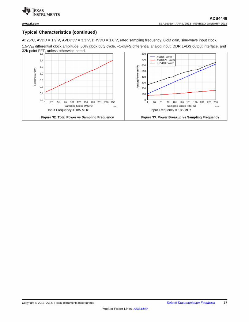
Typical Characteristics (continued)At 25°C, AVDD = 1.9 V, AVDD3V = 3.3 V, DRVDD = 1.8 V, rated sampling frequency, 0-dB gain, sine-wave input clock,
1.5-VPP differential clock amplitude, 50% clock duty cycle, –1-dBFS differential analog input, DDR LVDS output interface, and32k-point FFT, unless otherwise noted.
Input Frequency = 185 MHz
Figure 32. Total Power vs Sampling Frequency
Input Frequency = 185 MHz
Figure 33. Power Breakup vs Sampling Frequency
65.5
66
66
66
66.5
66.5
66.5
67
67
67
67.5
67.5
67.5
68
68
68
68.5
68.5
68.5
69
69
69
69.4
69.4
69.4
69.8
69.8
69.8
70.2
70.2
70.2
70.6
Input Frequency, MHz
Sam
plin
g F
requ
ency
, MS
PS
50 100 150 200 250 300 350 400 450
190
200
210
220
230
240
250
66 67 68 69 70
62.5
62.5
62.9
62.9
62.9
63.3
63.3
63.3
63.7
63.7
63.7
64.1
64.1
64.1
64.5
64.5
64.5
64.5
64.7
64.7
64.7
64.9
64.9
Input Frequency, MHz
Sam
plin
g F
requ
ency
, MS
PS
50 100 150 200 250 300 350 400 450
190
200
210
220
230
240
250
62.5 63 63.5 64 64.5
70
70
70
75
75
75
80
80
80
83
83
83
87
87
87
87
87
87
87
91
91
9187
87
87
95
91
Input Frequency, MHz
Sam
plin
g F
requ
ency
, MS
PS
50 100 150 200 250 300 350 400 450
190
200
210
220
230
240
250
70 75 80 85 90 95
76
76
76
79
79
79
82
82
82
84
84
84
86
86
86
88
88
88
90
90
90
Input Frequency, MHz
Sam
plin
g F
requ
ency
, MS
PS
50 100 150 200 250 300 350 400 450
190
200
210
220
230
240
250
74 76 78 80 82 84 86 88 90
18
ADS4449SBAS603A –APRIL 2013–REVISED JANUARY 2016 www.ti.com
Product Folder Links: ADS4449
Submit Documentation Feedback Copyright © 2013–2016, Texas Instruments Incorporated
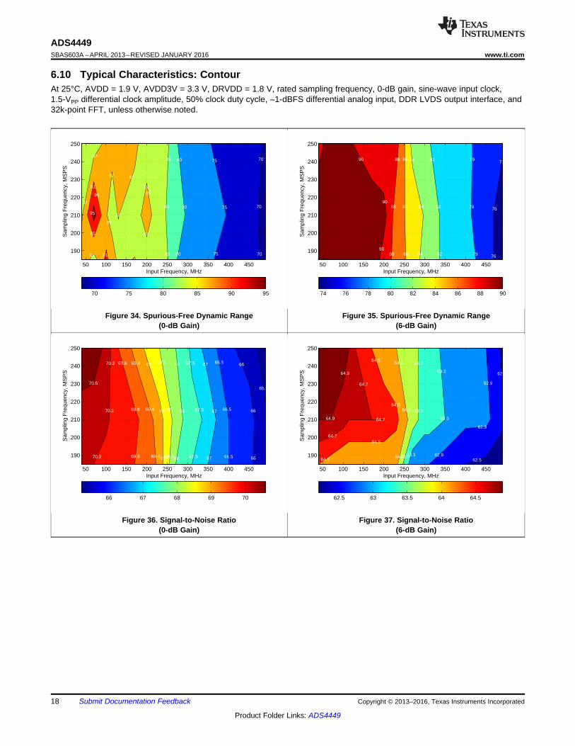
6.10 Typical Characteristics: ContourAt 25°C, AVDD = 1.9 V, AVDD3V = 3.3 V, DRVDD = 1.8 V, rated sampling frequency, 0-dB gain, sine-wave input clock,1.5-VPP differential clock amplitude, 50% clock duty cycle, –1-dBFS differential analog input, DDR LVDS output interface, and32k-point FFT, unless otherwise noted.
Figure 34. Spurious-Free Dynamic Range(0-dB Gain)
Figure 35. Spurious-Free Dynamic Range(6-dB Gain)
Figure 36. Signal-to-Noise Ratio(0-dB Gain)
Figure 37. Signal-to-Noise Ratio(6-dB Gain)

Ch B(Ch D)
InputClock
CLKOUTABM(CLKOUTCDM)
CLKOUTABP(CLKOUTCDP)
Output DataDABP, DABM
(DCDP, DCDM)
DDRLVDS
InputSignal
SampleN
N+1N+2 N+3 N+4
tA
CLKINM
CLKINP
N+10N+11
N+12
NN-1 N+1N-10 N-9 N-8 N-7
tPDI
Ch A(Ch C)
Ch B(Ch D)
Ch A(Ch C)
Ch B(Ch D)
Ch A(Ch C)
Ch B(Ch D)
Ch A(Ch C)
Ch B(Ch D)
Ch A(Ch C)
Ch A(Ch C)
Ch B(Ch D)
Ch A(Ch C)
Ch B(Ch D)
Ch A(Ch C)
Ch B(Ch D)
Ch A(Ch C)
Ch B(Ch D)
Ch A(Ch C)
10 Clock Cycles
DxnP
DxnM
GND
Logic 0VODL
Logic 1VODH
VOCM
19
ADS4449www.ti.com SBAS603A –APRIL 2013–REVISED JANUARY 2016
Product Folder Links: ADS4449
Submit Documentation FeedbackCopyright © 2013–2016, Texas Instruments Incorporated
(1) Timing parameters are ensured by design and characterization and are not tested in production.
7 Parameter Measurement Information
7.1 LVDS Output TimingFigure 38 shows a timing diagram of the LVDS output voltage levels. Figure 39 shows the latency described inthe Timing Requirements (1) table.
Figure 38. LVDS Output Voltage Levels
Figure 39. Latency Timing
All 14 data bits of one channel are included in the digital output interface at the same time, as shown inFigure 40. Channel A and C data are output on the rising edge of the output clock while channels B and D areoutput on the falling edge of the output clock.

CLKOUTABP
CLKOUTABM
DAB[13:0]P,DAB[13:0]M
DCD[13:0]P,DCD[13:0]M
CLKOUTCDP
CLKOUTCDM
Sample N Sample N + 1 Sample N + 2
Sample N Sample N + 1 Sample N + 2
DA[13:0]P,DA[13:0]M
DB[13:0]P,DB[13:0]M
DA[13:0]P,DA[13:0]M
DB[13:0]P,DB[13:0]M
DA[13:0]P,DA[13:0]M
DB[13:0]P,DB[13:0]M
DC[13:0]P,DC[13:0]M
DD[13:0]P,DD[13:0]M
DC[13:0]P,DC[13:0]M
DD[13:0]P,DD[13:0]M
DC[13:0]P,DC[13:0]M
DD[13:0]P,DD[13:0]M
20
ADS4449SBAS603A –APRIL 2013–REVISED JANUARY 2016 www.ti.com
Product Folder Links: ADS4449
Submit Documentation Feedback Copyright © 2013–2016, Texas Instruments Incorporated
LVDS Output Timing (continued)
Figure 40. LVDS Output Interface Timing

DAB0P, DAB0M orOVRABP, OVRABM
CLKINP,CLKINM
AINP,AINM
CommonMode
VCM
CLKOUTABP,CLKOUTABM
DAB[13:1]P,DAB[13:1]M
14
BINP,BINM
CINP,CINM
DINP,DINM
Configuration Registers
CLKOUTCDP,CLKOUTCDM
DCD[13:1]P,DCD[13:1]M
14
DigitalBlock
DCD0P, DCD0M orOVRCDP, OVRCDM
OutputFormatter
DDRLVDS
14-BitADC
14-BitADC
14-BitADC
14-BitADC
DigitalBlock
SC
LK
SE
N
SD
ATA
SD
OU
T
RE
SE
T
PD
N
21
ADS4449www.ti.com SBAS603A –APRIL 2013–REVISED JANUARY 2016
Product Folder Links: ADS4449
Submit Documentation FeedbackCopyright © 2013–2016, Texas Instruments Incorporated
8 Detailed Description
8.1 OverviewThe ADS4449 belong to TI’s low-power family of quad-channel, 14-bit, analog-to-digital converters (ADCs). Highperformance is maintained while power is reduced for power-sensitive applications. In addition to its low powerand high performance, the ADS4449 has a number of digital features and operating modes to enable designflexibility.
At every falling edge of the input clock, the analog input signal for each channel is sampled simultaneously. Thesampled signal in each channel is converted by a pipeline of low-resolution stages. In each stage, the sampled-and-held signal is converted by a high-speed, low-resolution, flash sub-ADC. The difference (residue) betweenthe stage input and quantized equivalent is gained and propagates to the next stage. At every clock, eachsubsequent stage resolves the sampled input with greater accuracy. The digital outputs from all stages arecombined in a digital correction logic block and are digitally processed to create the final code, after a datalatency of 10 clock cycles. The digital output is available in a double data rate (DDR) low-voltage differentialsignaling (LVDS) interface and is coded in binary twos complement format.
The ADS4449 can be configured with a serial programming interface (SPI), as described in the Serial Interfacesection. In addition, the device has control terminals that control power-down.
8.2 Functional Block Diagram
DA[13:0]P, DA[13:0]M
DB[13:0]P, DB[13:0]M
DA[13:0]P, DA[13:0]M
DB[13:0]P, DB[13:0]M
Sample N Sample N+1
14-Bit Output
CLKOUTP
CLKOUTM
DA[13:0]P, DA[13:0]MDB[13:0]P, DB[13:0]M
DA[13:1]P, DA[13:1]M
DB[13:1]P, DB[13:1]M
DA[13:1]P, DA[13:1]M
DB[13:1]P, DB[13:1]M
Sample N Sample N+1
OVR A OVR B OVR A OVR B
CLKOUTP
CLKOUTM
DA[13:1]P, DA[13:1]MDB[13:1]P, DB[13:1]M
DAB0P, DAB0M
13-Bit Output
Overrange Indicator
22
ADS4449SBAS603A –APRIL 2013–REVISED JANUARY 2016 www.ti.com
Product Folder Links: ADS4449
Submit Documentation Feedback Copyright © 2013–2016, Texas Instruments Incorporated
8.3 Feature Description
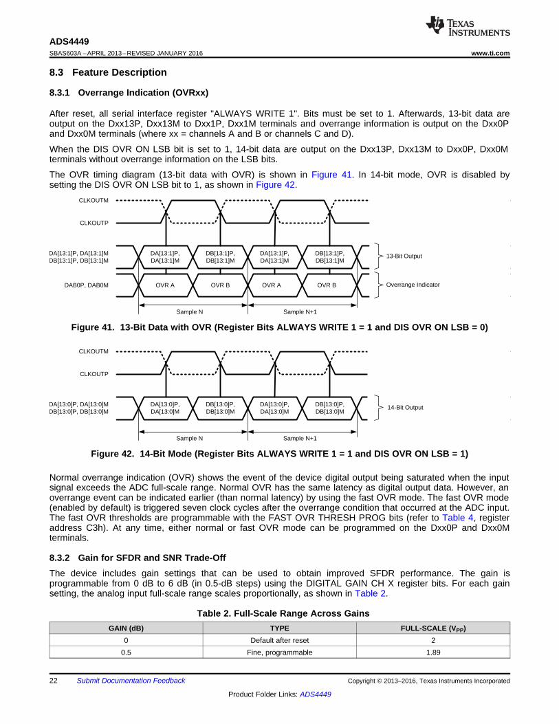
8.3.1 Overrange Indication (OVRxx)
After reset, all serial interface register "ALWAYS WRITE 1". Bits must be set to 1. Afterwards, 13-bit data areoutput on the Dxx13P, Dxx13M to Dxx1P, Dxx1M terminals and overrange information is output on the Dxx0Pand Dxx0M terminals (where xx = channels A and B or channels C and D).
When the DIS OVR ON LSB bit is set to 1, 14-bit data are output on the Dxx13P, Dxx13M to Dxx0P, Dxx0Mterminals without overrange information on the LSB bits.
The OVR timing diagram (13-bit data with OVR) is shown in Figure 41. In 14-bit mode, OVR is disabled bysetting the DIS OVR ON LSB bit to 1, as shown in Figure 42.
Figure 41. 13-Bit Data with OVR (Register Bits ALWAYS WRITE 1 = 1 and DIS OVR ON LSB = 0)
Figure 42. 14-Bit Mode (Register Bits ALWAYS WRITE 1 = 1 and DIS OVR ON LSB = 1)
Normal overrange indication (OVR) shows the event of the device digital output being saturated when the inputsignal exceeds the ADC full-scale range. Normal OVR has the same latency as digital output data. However, anoverrange event can be indicated earlier (than normal latency) by using the fast OVR mode. The fast OVR mode(enabled by default) is triggered seven clock cycles after the overrange condition that occurred at the ADC input.The fast OVR thresholds are programmable with the FAST OVR THRESH PROG bits (refer to Table 4, registeraddress C3h). At any time, either normal or fast OVR mode can be programmed on the Dxx0P and Dxx0Mterminals.
8.3.2 Gain for SFDR and SNR Trade-OffThe device includes gain settings that can be used to obtain improved SFDR performance. The gain isprogrammable from 0 dB to 6 dB (in 0.5-dB steps) using the DIGITAL GAIN CH X register bits. For each gainsetting, the analog input full-scale range scales proportionally, as shown in Table 2.
Table 2. Full-Scale Range Across GainsGAIN (dB) TYPE FULL-SCALE (VPP)
0 Default after reset 20.5 Fine, programmable 1.89
23
ADS4449www.ti.com SBAS603A –APRIL 2013–REVISED JANUARY 2016
Product Folder Links: ADS4449
Submit Documentation FeedbackCopyright © 2013–2016, Texas Instruments Incorporated
Feature Description (continued)Table 2. Full-Scale Range Across Gains (continued)
GAIN (dB) TYPE FULL-SCALE (VPP)1 Fine, programmable 1.78
1.5 Fine, programmable 1.682 Fine, programmable 1.59
2.5 Fine, programmable 1.53 Fine, programmable 1.42
3.5 Fine, programmable 1.344 Fine, programmable 1.26
4.5 Fine, programmable 1.195 Fine, programmable 1.12
5.5 Fine, programmable 1.066 Fine, programmable 1
(1) See the Serial Interface section for details.(2) High SNR mode improves SNR typically by 1 dB at 170 MHz input frequency. See the Using High SNR Mode Register Settings section.
SFDR improvement is achieved at the expense of SNR; for each gain setting, SNR degrades by approximately0.5 dB to 1 dB. SNR degradation is diminished at high input frequencies. As a result, fine gain is very useful athigh input frequencies because SFDR improvement is significant with marginal degradation in SNR. Therefore,fine gain can be used to trade-off between SFDR and SNR.
After a reset, the gain function is disabled. To use fine gain:• First, program the DIGITAL ENABLE bits to enable digital functions.• This setting enables the gain for all four channels and places the device in a 0-dB gain mode.• For other gain settings, program the DIGITAL GAIN CH X register bits.
8.4 Device Functional Modes
8.4.1 Special Performance ModesBest performance can be achieved by writing certain modes depending upon source impedance, band ofoperation and sampling speed. Table 3 summarizes the different these modes.
Table 3. High-Performance Modes Summary (1)
SPECIAL MODES SUMMARY
SPECIAL MODE NAME ADDRESS (Hex) DATA (Hex) INPUT FREQUENCIES(Up to 125 MHz)
INPUT FREQUENCIES(> 125 MHz)
High-frequency mode F1 20 Not required Must
High SNR mode (2)
58 20 Optional Optional70 20 Optional Optional88 20 Optional OptionalA0 20 Optional Optional
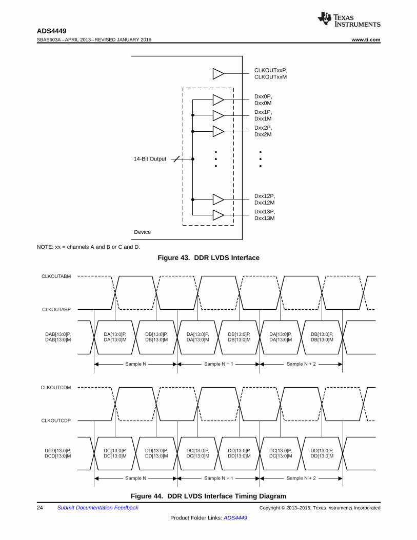
8.4.2 Digital Output InformationThe device provides 14-bit digital data for each channel and two output clocks in LVDS mode. Output terminalsare shared by a pair of channels that are accompanied by one dedicated output clock.
8.4.2.1 DDR LVDS OutputsIn the LVDS interface mode, the data bits and clock are output using LVDS levels. The data bits of two channelsare multiplexed and output on each LVDS differential pair of terminals; see Figure 43 and Figure 44.
CLKOUTABP
CLKOUTABM
DAB[13:0]P,DAB[13:0]M
DCD[13:0]P,DCD[13:0]M
CLKOUTCDP
CLKOUTCDM
Sample N Sample N + 1 Sample N + 2
Sample N Sample N + 1 Sample N + 2
DA[13:0]P,DA[13:0]M
DB[13:0]P,DB[13:0]M
DA[13:0]P,DA[13:0]M
DB[13:0]P,DB[13:0]M
DA[13:0]P,DA[13:0]M
DB[13:0]P,DB[13:0]M
DC[13:0]P,DC[13:0]M
DD[13:0]P,DD[13:0]M
DC[13:0]P,DC[13:0]M
DD[13:0]P,DD[13:0]M
DC[13:0]P,DC[13:0]M
DD[13:0]P,DD[13:0]M
Dxx0P,Dxx0M
Dxx1P,Dxx1M
Dxx2P,Dxx2M
Dxx12P,Dxx12M
Dxx13P,Dxx13M
CLKOUTxxP,CLKOUTxxM
14-Bit Output
Device
24
ADS4449SBAS603A –APRIL 2013–REVISED JANUARY 2016 www.ti.com
Product Folder Links: ADS4449
Submit Documentation Feedback Copyright © 2013–2016, Texas Instruments Incorporated
NOTE: xx = channels A and B or C and D.
Figure 43. DDR LVDS Interface
Figure 44. DDR LVDS Interface Timing Diagram

−120
−100
−80
−60
−40
−20
0
0 25 50 75 100 125Frequency (MHz)
Am
plitu
de (
dBF
S)
G036
−120
−100
−80
−60
−40
−20
0
0 25 50 75 100 125Frequency (MHz)
Am
plitu
de (
dBF
S)
G037
VDIFF(high)
VDIFF(low)
1.1 V
High
Low
Low
OUTP
OUTM
ROUT
External
100- LoadW
High
25
ADS4449www.ti.com SBAS603A –APRIL 2013–REVISED JANUARY 2016
Product Folder Links: ADS4449
Submit Documentation FeedbackCopyright © 2013–2016, Texas Instruments Incorporated
8.4.2.1.1 LVDS Output Data and Clock Buffers
The equivalent circuit of each LVDS output buffer is shown in Figure 45. After reset, the buffer presents anoutput impedance of 100 Ω to match with the external 100-Ω termination.
The VDIFF voltage is nominally 350 mV, resulting in an output swing of ±350 mV with 100-Ω external termination.The VDIFF voltage is programmable using the LVDS SWING register bits (refer to Table 4, register address 01h).The buffer output impedance behaves similar to a source-side series termination. By absorbing reflections fromthe receiver end, the source-side termination helps improve signal integrity.
Figure 45. LVDS Buffer Equivalent Circuit
8.4.2.1.2 Output Data Format
The device transmits data in binary twos complement format. In the event of an input voltage overdrive, thedigital outputs go to the appropriate full-scale level. For a positive overdrive, the output code is 3FFh. For anegative input overdrive, the output code is 400h.
8.4.3 Using High SNR Mode Register SettingsThe HIGH SNR MODE register settings can be used to further improve the SNR. However, there is a trade offbetween improved SNR and degraded THD when these settings are used. These settings shut down the internalspectrum-cleaning algorithm, resulting in THD performance degradation. Figure 46 and Figure 47 show the effectof using HIGH SNR MODE. SNR improves by approximately 1 dB and THD degrades by 3 dB.
fIN = 170 MHz SFDR = 93 dBc SNR = 69.1 dBFSSINAD = 69 dBFS THD = 89 dBc
Figure 46. FFT (Default) at 170 MHz
fIN = 170 MHz SFDR = 89 dBc SNR = 70.1 dBFSSINAD = 70 dBFS THD = 86 dBc
Figure 47. FFT with High SNR Mode at 170 MHz
Figure 48 shows SNR versus input frequency with and without these settings.

64
65
66
67
68
69
70
71
72
40 90 140 190 240 290 340 390 440 490Input Frequency (MHz)
SN
R (
dBF
S)
DefaultHIGH SNR MODE Enable
G038
26
ADS4449SBAS603A –APRIL 2013–REVISED JANUARY 2016 www.ti.com
Product Folder Links: ADS4449
Submit Documentation Feedback Copyright © 2013–2016, Texas Instruments Incorporated
Figure 48. SNR vs Input Frequency with High SNR Mode
To obtain best performance, TI recommends keeping termination impedance between INP and INM low (forinstance, at 50 Ω differential). This setting helps absorb the kickback noise component of the spectrum-cleaningalgorithm. However, when higher termination impedances (such as 100 Ω) are required, shutting down thespectrum-cleaning algorithm by using the HIGH SNR MODE register settings can be helpful.
8.4.4 Input Common ModeTo ensure a low-noise, common-mode reference, the VCM terminal should be filtered with a 0.1-µF, low-inductance capacitor connected to ground. The VCM terminal is designed to directly bias the ADC inputs (refer toFigure 54 to Figure 57).
Each ADC input terminal sinks a common-mode current of approximately 1.5 µA per MSPS of clock frequency.When a differential amplifier is used to drive the ADC (with dc-coupling), ensure that the output common-mode ofthe amplifier is within the acceptable input common-mode range of the ADC inputs (VCM ± 25 mV).
8.5 Programming
8.5.1 Serial InterfaceThe device has a set of internal registers that can be accessed by the serial interface formed by the SEN (serialinterface enable), SCLK (serial interface clock), SDATA (serial interface input data), and SDOUT (serial interfacereadback data) terminals. Serially shifting bits into the device is enabled when SEN is low. Serial data (SDATA)are latched at every SCLK falling edge when SEN is active (low). Serial data are loaded into the register at every16th SCLK falling edge when SEN is low. When the word length exceeds a multiple of 16 bits, the excess bitsare ignored. Data can be loaded in multiples of 16-bit words within a single active SEN pulse. The first eight bitsform the register address and the remaining eight bits are the register data. The interface can function with SCLKfrequencies from 20 MHz down to very low speeds (of a few hertz) and also with a non-50% SCLK duty cycle.
8.5.1.1 Register InitializationAfter power-up, the internal registers must be initialized to the default values. This initialization can beaccomplished in one of two ways:1. Either through a hardware reset by applying a high pulse on the RESET terminal (of widths greater than
10ns), as shown in Figure 1; or2. By applying a software reset. When using the serial interface, set the RESET bit (D1 in register 00h) high.
This setting initializes the internal registers to the default values and then self-resets the RESET bit low. Inthis case, the RESET terminal is kept low.
SCLK
SDOUT
tSD_DELAY
SDATA
SCLK
SEN
a) Enable serial readout (READOUT = 1)
A7 A6 A5 A4 A3 A2 A1 A0 D7 D6 D5 D4 D3 D2 D1 D0SDATA
SCLK
SEN
SDOUT
b) Read contents of Register 45h. This register is initialized with 04h.
SDOUT 0 0 0 0 0 00 1
Register Address A[7:0] = 00h Register Data D[7:0] = 01h
Register Address A[7:0] = 45h Register Data D[7:0] = XX (don’t care)
The SDOUT pin is in a high-impedance state (READOUT = 0).
The SDOUT pin functions as a serial readout (READOUT = 1).
A7 A6 A5 A4 A3 A2 A1 A0 D7 D6 D5 D4 D3 D2 D1 D0
27
ADS4449www.ti.com SBAS603A –APRIL 2013–REVISED JANUARY 2016
Product Folder Links: ADS4449
Submit Documentation FeedbackCopyright © 2013–2016, Texas Instruments Incorporated
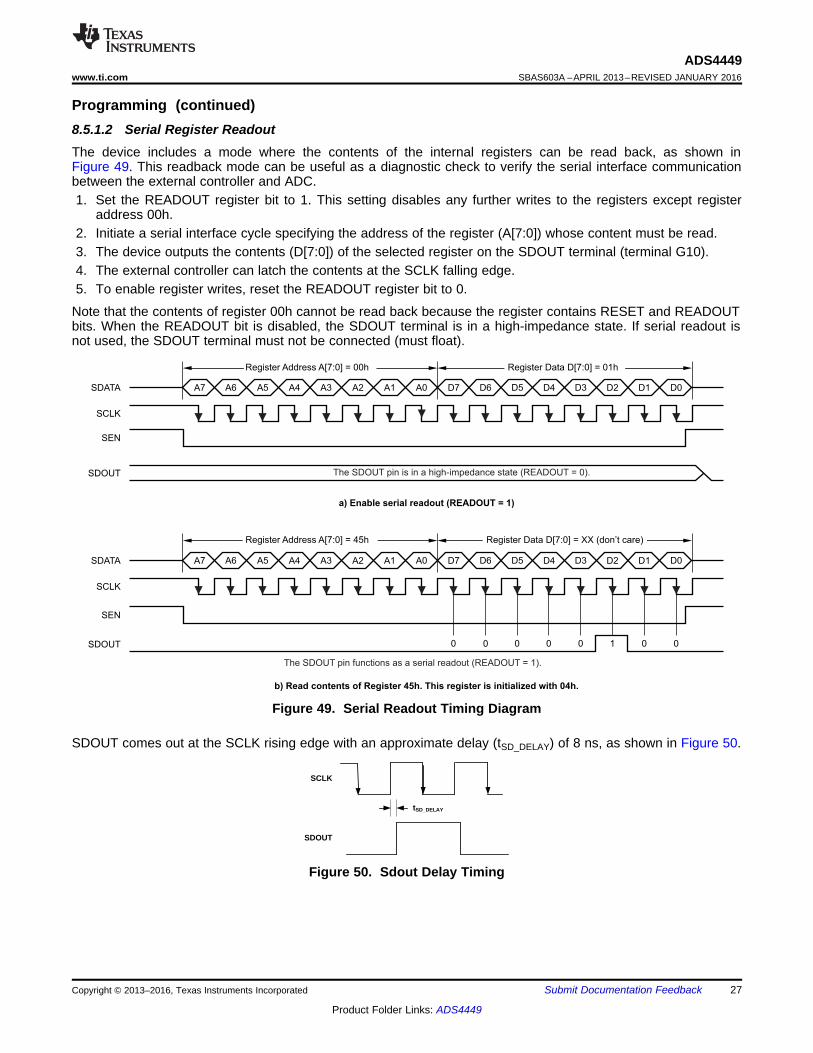
Programming (continued)8.5.1.2 Serial Register ReadoutThe device includes a mode where the contents of the internal registers can be read back, as shown inFigure 49. This readback mode can be useful as a diagnostic check to verify the serial interface communicationbetween the external controller and ADC.1. Set the READOUT register bit to 1. This setting disables any further writes to the registers except register
address 00h.2. Initiate a serial interface cycle specifying the address of the register (A[7:0]) whose content must be read.3. The device outputs the contents (D[7:0]) of the selected register on the SDOUT terminal (terminal G10).4. The external controller can latch the contents at the SCLK falling edge.5. To enable register writes, reset the READOUT register bit to 0.
Note that the contents of register 00h cannot be read back because the register contains RESET and READOUTbits. When the READOUT bit is disabled, the SDOUT terminal is in a high-impedance state. If serial readout isnot used, the SDOUT terminal must not be connected (must float).
Figure 49. Serial Readout Timing Diagram
SDOUT comes out at the SCLK rising edge with an approximate delay (tSD_DELAY) of 8 ns, as shown in Figure 50.
Figure 50. Sdout Delay Timing
28
ADS4449SBAS603A –APRIL 2013–REVISED JANUARY 2016 www.ti.com
Product Folder Links: ADS4449
Submit Documentation Feedback Copyright © 2013–2016, Texas Instruments Incorporated
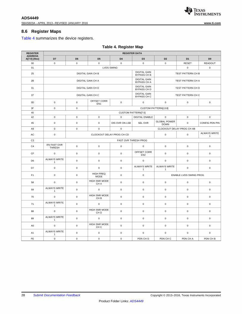
8.6 Register MapsTable 4 summarizes the device registers.
Table 4. Register MapREGISTERADDRESS
A[7:0] (Hex)
REGISTER DATA
D7 D6 D5 D4 D3 D2 D1 D0
00 0 0 0 0 0 0 RESET READOUT
01 LVDS SWING 0 0
25 DIGITAL GAIN CH B DIGITAL GAINBYPASS CH B TEST PATTERN CH B
2B DIGITAL GAIN CH A DIGITAL GAINBYPASS CH A TEST PATTERN CH A
31 DIGITAL GAIN CH D DIGITAL GAINBYPASS CH D TEST PATTERN CH D
37 DIGITAL GAIN CH C DIGITAL GAINBYPASS CH C TEST PATTERN CH C
3D 0 0 OFFSET CORREN1 0 0 0 0 0
3F 0 0 CUSTOM PATTERN[13:8]
40 CUSTOM PATTERN[7:0]
42 0 0 0 0 DIGITAL ENABLE 0 0 0
45 0 0 0 DIS OVR ON LSB SEL OVR GLOBAL POWERDOWN 0 CONFIG PDN PIN
A9 0 0 0 0 CLOCKOUT DELAY PROG CH AB
AC 0 CLOCKOUT DELAY PROG CH CD 0 0 ALWAYS WRITE1
C3 FAST OVR THRESH PROG
C4 EN FAST OVRTHRESH 0 0 0 0 0 0 0
CF 0 0 0 0 OFFSET CORREN2 0 0 0
D6 ALWAYS WRITE1 0 0 0 0 0 0 0
D7 0 0 0 0 ALWAYS WRITE1
ALWAYS WRITE1 0 0
F1 0 0 HIGH FREQMODE 0 0 ENABLE LVDS SWING PROG
58 0 0 HIGH SNR MODECH A 0 0 0 0 0
59 ALWAYS WRITE1 0 0 0 0 0 0 0
70 0 0 HIGH SNR MODECH B 0 0 0 0 0
71 ALWAYS WRITE1 0 0 0 0 0 0 0
88 0 0 HIGH SNR MODECH D 0 0 0 0 0
89 ALWAYS WRITE1 0 0 0 0 0 0 0
A0 0 0 HIGH SNR MODECH C 0 0 0 0 0
A1 ALWAYS WRITE1 0 0 0 0 0 0 0
FE 0 0 0 0 PDN CH D PDN CH C PDN CH A PDN CH B
29
ADS4449www.ti.com SBAS603A –APRIL 2013–REVISED JANUARY 2016
Product Folder Links: ADS4449
Submit Documentation FeedbackCopyright © 2013–2016, Texas Instruments Incorporated
8.6.1 Register Description
8.6.1.1 Register Address 00h (Default = 00h)
7 6 5 4 3 2 1 00 0 0 0 0 0 RESET READOUT
Bits 7-2 Always write 0Bit 1 RESET: Software reset applied
This bit resets all internal registers to the default values and self-clears to 0.Bit 0 READOUT: Serial readout
This bit sets the serial readout of the registers.0 = Serial readout of registers disabled; the SDOUT terminal is placed in a high-impedance state. (default)1 = Serial readout enabled; the SDOUT terminal functions as a serial data readout withCMOS logic levels running from the DRVDD supply.
8.6.1.2 Register Address 01h (Default = 00h)
7 6 5 4 3 2 1 0LVDS SWING 0 0
Bits 7-2 LVDS SWING: LVDS swing programmabilityThese bits program the LVDS swing only after the ENABLE LVDS SWING PROG bitsare set to 11.000000 = Default LVDS swing; ±350 mV with an external 100-Ω termination (default)011011 = ±420-mV LVDS swing with an external 100-Ω termination110010 = ±470-mV LVDS swing with an external 100-Ω termination010100 = ±560-mV LVDS swing with an external 100-Ω termination001111 = ±160-mV LVDS swing with an external 100-Ω termination
Bits 1-0 Always write 0
8.6.1.3 Register Address 25h (Default = 00h)
7 6 5 4 3 2 1 0
DIGITAL GAIN CH B DIGITAL GAINBYPASS CH B TEST PATTERN CH B
Bits 7-4 DIGITAL GAIN CH B: Channel B digital gain programmabilityThese bits set the digital gain programmability from 0 dB to 6 dB in 0.5-dB steps forchannel B. Set the DIGITAL ENABLE bit to 1 beforehand to enable this feature.0000 = 0-dB gain (default)0001 = 0.5-dB gain0010 = 1-dB gain0011 = 1.5-dB gain0100 = 2-dB gain0101 = 2.5-dB gain0110 = 3-dB gain0111 = 3.5-dB gain1000 = 4-dB gain1001 = 4.5-dB gain1010 = 5-dB gain1011 = 5.5-dB gain1100 = 6-dB gain
30
ADS4449SBAS603A –APRIL 2013–REVISED JANUARY 2016 www.ti.com
Product Folder Links: ADS4449
Submit Documentation Feedback Copyright © 2013–2016, Texas Instruments Incorporated
Bit 3 DIGITAL GAIN BYPASS CH B: Channel B digital gain bypass0 = Normal operation (default)1 = Digital gain feature for channel B is bypassed
Bits 2-0 TEST PATTERN CH B: Channel B test pattern programmabilityThese bits program the test pattern for channel B.000 = Normal operation (default)001 = Outputs all 0s010 = Outputs all 1s011 = Outputs toggle pattern
Output data ([D:0]) are an alternating sequence of 01010101010101 and10101010101010.
100 = Outputs digital rampOutput data increments by one 14-bit LSB every clock cycle from code 0 to code16383
101 = Outputs custom patternTo program a test pattern, use the CUSTOM PATTERN D[13:0] bits of registers 3Fhand 40h.
110 = Unused111 = Unused

31
ADS4449www.ti.com SBAS603A –APRIL 2013–REVISED JANUARY 2016
Product Folder Links: ADS4449
Submit Documentation FeedbackCopyright © 2013–2016, Texas Instruments Incorporated
8.6.1.4 Register Address 2bh (Default = 00h)
7 6 5 4 3 2 1 0
DIGITAL GAIN CH A DIGITAL GAINBYPASS CH A TEST PATTERN CH A
Bits 7-4 DIGITAL GAIN CH A: Channel A digital gain programmabilityThese bits set the digital gain programmability from 0 dB to 6 dB in 0.5-dB steps forchannel A. Set the DIGITAL ENABLE bit to 1 beforehand to enable this feature.0000 = 0-dB gain (default)0001 = 0.5-dB gain0010 = 1-dB gain0011 = 1.5-dB gain0100 = 2-dB gain0101 = 2.5-dB gain0110 = 3-dB gain0111 = 3.5-dB gain1000 = 4-dB gain1001 = 4.5-dB gain1010 = 5-dB gain1011 = 5.5-dB gain1100 = 6-dB gain
Bit 3 DIGITAL GAIN BYPASS CH A: Channel A digital gain bypass0 = Normal operation (default)1 = Digital gain feature for channel A is bypassed
Bits 2-0 TEST PATTERN CH A: Channel A test pattern programmabilityThese bits program the test pattern for channel A.000 = Normal operation (default)001 = Outputs all 0s010 = Outputs all 1s011 = Outputs toggle pattern
Output data ([D:0]) are an alternating sequence of 01010101010101 and10101010101010.
100 = Outputs digital rampOutput data increments by one 14-bit LSB every clock cycle from code 0 to code16383
101 = Outputs custom patternTo program a test pattern, use the CUSTOM PATTERN D[13:0] bits of registers 3Fhand 40h.
110 = Unused111 = Unused
32
ADS4449SBAS603A –APRIL 2013–REVISED JANUARY 2016 www.ti.com
Product Folder Links: ADS4449
Submit Documentation Feedback Copyright © 2013–2016, Texas Instruments Incorporated
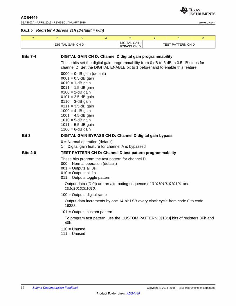
8.6.1.5 Register Address 31h (Default = 00h)
7 6 5 4 3 2 1 0
DIGITAL GAIN CH D DIGITAL GAINBYPASS CH D TEST PATTERN CH D
Bits 7-4 DIGITAL GAIN CH D: Channel D digital gain programmabilityThese bits set the digital gain programmability from 0 dB to 6 dB in 0.5-dB steps forchannel D. Set the DIGITAL ENABLE bit to 1 beforehand to enable this feature.0000 = 0-dB gain (default)0001 = 0.5-dB gain0010 = 1-dB gain0011 = 1.5-dB gain0100 = 2-dB gain0101 = 2.5-dB gain0110 = 3-dB gain0111 = 3.5-dB gain1000 = 4-dB gain1001 = 4.5-dB gain1010 = 5-dB gain1011 = 5.5-dB gain1100 = 6-dB gain
Bit 3 DIGITAL GAIN BYPASS CH D: Channel D digital gain bypass0 = Normal operation (default)1 = Digital gain feature for channel A is bypassed
Bits 2-0 TEST PATTERN CH D: Channel D test pattern programmabilityThese bits program the test pattern for channel D.000 = Normal operation (default)001 = Outputs all 0s010 = Outputs all 1s011 = Outputs toggle pattern
Output data ([D:0]) are an alternating sequence of 01010101010101 and10101010101010.
100 = Outputs digital rampOutput data increments by one 14-bit LSB every clock cycle from code 0 to code16383
101 = Outputs custom patternTo program test pattern, use the CUSTOM PATTERN D[13:0] bits of registers 3Fh and40h.
110 = Unused111 = Unused
33
ADS4449www.ti.com SBAS603A –APRIL 2013–REVISED JANUARY 2016
Product Folder Links: ADS4449
Submit Documentation FeedbackCopyright © 2013–2016, Texas Instruments Incorporated
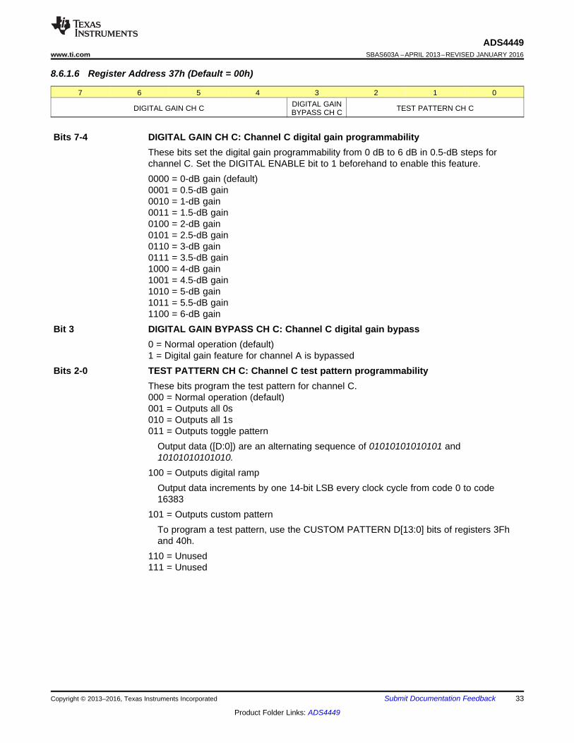
8.6.1.6 Register Address 37h (Default = 00h)
7 6 5 4 3 2 1 0
DIGITAL GAIN CH C DIGITAL GAINBYPASS CH C TEST PATTERN CH C
Bits 7-4 DIGITAL GAIN CH C: Channel C digital gain programmabilityThese bits set the digital gain programmability from 0 dB to 6 dB in 0.5-dB steps forchannel C. Set the DIGITAL ENABLE bit to 1 beforehand to enable this feature.0000 = 0-dB gain (default)0001 = 0.5-dB gain0010 = 1-dB gain0011 = 1.5-dB gain0100 = 2-dB gain0101 = 2.5-dB gain0110 = 3-dB gain0111 = 3.5-dB gain1000 = 4-dB gain1001 = 4.5-dB gain1010 = 5-dB gain1011 = 5.5-dB gain1100 = 6-dB gain
Bit 3 DIGITAL GAIN BYPASS CH C: Channel C digital gain bypass0 = Normal operation (default)1 = Digital gain feature for channel A is bypassed
Bits 2-0 TEST PATTERN CH C: Channel C test pattern programmabilityThese bits program the test pattern for channel C.000 = Normal operation (default)001 = Outputs all 0s010 = Outputs all 1s011 = Outputs toggle pattern
Output data ([D:0]) are an alternating sequence of 01010101010101 and10101010101010.
100 = Outputs digital rampOutput data increments by one 14-bit LSB every clock cycle from code 0 to code16383
101 = Outputs custom patternTo program a test pattern, use the CUSTOM PATTERN D[13:0] bits of registers 3Fhand 40h.
110 = Unused111 = Unused
34
ADS4449SBAS603A –APRIL 2013–REVISED JANUARY 2016 www.ti.com
Product Folder Links: ADS4449
Submit Documentation Feedback Copyright © 2013–2016, Texas Instruments Incorporated
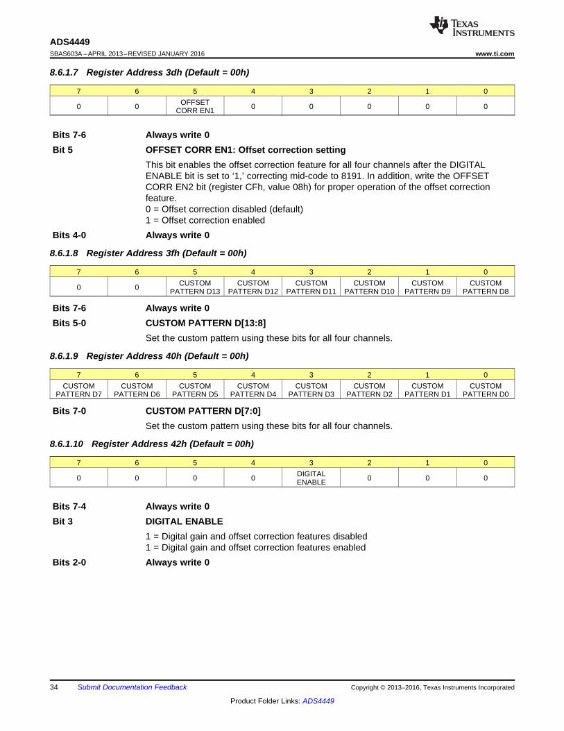
8.6.1.7 Register Address 3dh (Default = 00h)
7 6 5 4 3 2 1 0
0 0 OFFSETCORR EN1 0 0 0 0 0
Bits 7-6 Always write 0Bit 5 OFFSET CORR EN1: Offset correction setting
This bit enables the offset correction feature for all four channels after the DIGITALENABLE bit is set to ‘1,’ correcting mid-code to 8191. In addition, write the OFFSETCORR EN2 bit (register CFh, value 08h) for proper operation of the offset correctionfeature.0 = Offset correction disabled (default)1 = Offset correction enabled
Bits 4-0 Always write 0
8.6.1.8 Register Address 3fh (Default = 00h)
7 6 5 4 3 2 1 0
0 0 CUSTOMPATTERN D13
CUSTOMPATTERN D12
CUSTOMPATTERN D11
CUSTOMPATTERN D10
CUSTOMPATTERN D9
CUSTOMPATTERN D8
Bits 7-6 Always write 0Bits 5-0 CUSTOM PATTERN D[13:8]
Set the custom pattern using these bits for all four channels.
8.6.1.9 Register Address 40h (Default = 00h)
7 6 5 4 3 2 1 0CUSTOM
PATTERN D7CUSTOM
PATTERN D6CUSTOM
PATTERN D5CUSTOM
PATTERN D4CUSTOM
PATTERN D3CUSTOM
PATTERN D2CUSTOM
PATTERN D1CUSTOM
PATTERN D0
Bits 7-0 CUSTOM PATTERN D[7:0]Set the custom pattern using these bits for all four channels.
8.6.1.10 Register Address 42h (Default = 00h)
7 6 5 4 3 2 1 0
0 0 0 0 DIGITALENABLE 0 0 0
Bits 7-4 Always write 0Bit 3 DIGITAL ENABLE
1 = Digital gain and offset correction features disabled1 = Digital gain and offset correction features enabled
Bits 2-0 Always write 0

35
ADS4449www.ti.com SBAS603A –APRIL 2013–REVISED JANUARY 2016
Product Folder Links: ADS4449
Submit Documentation FeedbackCopyright © 2013–2016, Texas Instruments Incorporated
8.6.1.11 Register Address 45h (Default = 00h)
7 6 5 4 3 2 1 0
0 0 0 DIS OVR ONLSB SEL OVR
GLOBALPOWERDOWN
0 CONFIG PDNPIN
Bits 7-5 Always write 0Bit 4 DIS OVR ON LSB
0 = Effective ADC resolution is 13 bits (the LSB of a 14-bit output is OVR) (default)1 = ADC resolution is 14 bits
Bit 3 SEL OVR: OVR selection0 = Fast OVR selected (default)1 = Normal OVR selected. See the Overrange Indication (OVRxx) section for details.
Bit 2 GLOBAL POWER DOWN0 = Normal operation (default)1 = Global power down. All ADC channels, internal references, and output buffers arepowered down. Wakeup time from this mode is slow (100 µs).
Bit 1 Always write 0Bit 0 CONFIG PDN PIN
Use this bit to configure PDN terminal.0 = The PDN terminal functions as a standby terminal. All channels are put in standby.Wake-up time from standby mode is fast (10 µs). (default)1 = The PDN terminal functions as a global power-down terminal. All ADC channels,internal references, and output buffers are powered down. Wake-up time from globalpower mode is slow (100 µs).
8.6.1.12 Register Address A9h (Default = 00h)
7 6 5 4 3 2 1 00 0 0 0 CLOCKOUT DELAY PROG CH AB
Bits 7-4 Always write 0Bits 3-0 CLOCKOUT DELAY PROG CH AB
These bits program the clock out delay for channels A and B, see Table 5.
36
ADS4449SBAS603A –APRIL 2013–REVISED JANUARY 2016 www.ti.com
Product Folder Links: ADS4449
Submit Documentation Feedback Copyright © 2013–2016, Texas Instruments Incorporated
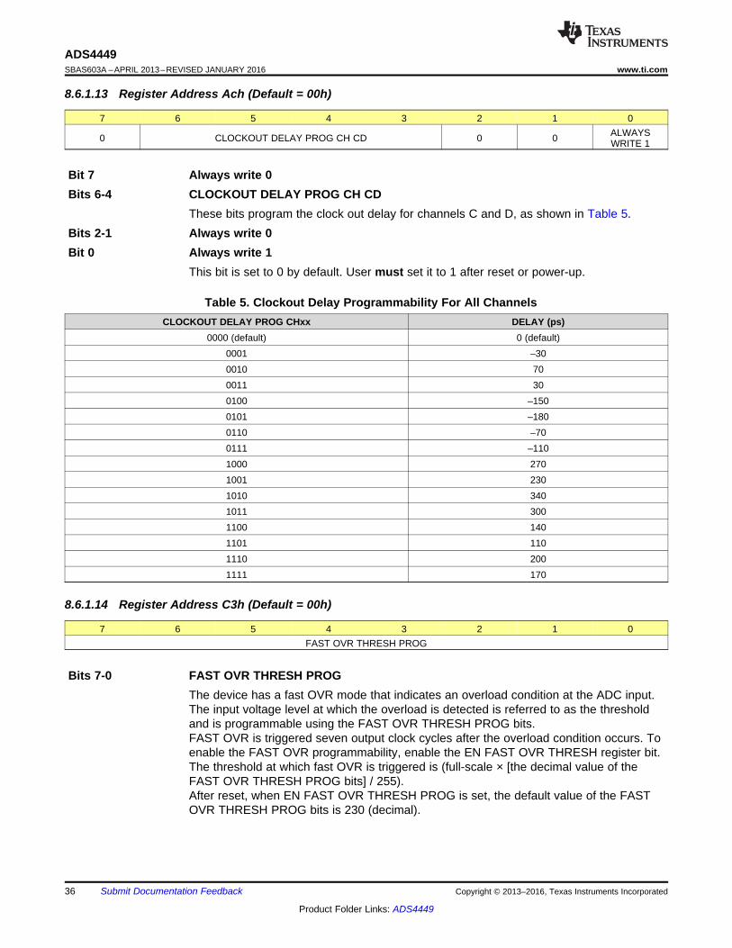
8.6.1.13 Register Address Ach (Default = 00h)
7 6 5 4 3 2 1 0
0 CLOCKOUT DELAY PROG CH CD 0 0 ALWAYSWRITE 1
Bit 7 Always write 0Bits 6-4 CLOCKOUT DELAY PROG CH CD
These bits program the clock out delay for channels C and D, as shown in Table 5.Bits 2-1 Always write 0Bit 0 Always write 1
This bit is set to 0 by default. User must set it to 1 after reset or power-up.
Table 5. Clockout Delay Programmability For All ChannelsCLOCKOUT DELAY PROG CHxx DELAY (ps)
0000 (default) 0 (default)0001 –300010 700011 300100 –1500101 –1800110 –700111 –1101000 2701001 2301010 3401011 3001100 1401101 1101110 2001111 170
8.6.1.14 Register Address C3h (Default = 00h)
7 6 5 4 3 2 1 0FAST OVR THRESH PROG
Bits 7-0 FAST OVR THRESH PROGThe device has a fast OVR mode that indicates an overload condition at the ADC input.The input voltage level at which the overload is detected is referred to as the thresholdand is programmable using the FAST OVR THRESH PROG bits.FAST OVR is triggered seven output clock cycles after the overload condition occurs. Toenable the FAST OVR programmability, enable the EN FAST OVR THRESH register bit.The threshold at which fast OVR is triggered is (full-scale × [the decimal value of theFAST OVR THRESH PROG bits] / 255).After reset, when EN FAST OVR THRESH PROG is set, the default value of the FASTOVR THRESH PROG bits is 230 (decimal).

37
ADS4449www.ti.com SBAS603A –APRIL 2013–REVISED JANUARY 2016
Product Folder Links: ADS4449
Submit Documentation FeedbackCopyright © 2013–2016, Texas Instruments Incorporated
8.6.1.15 Register Address C4h (Default = 00h)
7 6 5 4 3 2 1 0EN FAST OVR
THRESH 0 0 0 0 0 0 0
Bit 7 EN FAST OVR THRESHThis bit enables the device to be programmed to select the fast OVR threshold.
Bits 6-0 Always write 0
8.6.1.16 Register Address Cfh (Default = 00h)
7 6 5 4 3 2 1 0
0 0 0 0 OFFSETCORR EN2 0 0 0
Bits 7-4 Always write 0Bit 3 OFFSET CORR EN2
This bit must be set to ‘1’ when the OFFSET CORR EN1 bit is selected.Bits 2-0 Always write 0
8.6.1.17 Register Address D6h (Default = 00h)
7 6 5 4 3 2 1 0ALWAYSWRITE 1 0 0 0 0 0 0 0
Bits 7 Always write 1This bit is set to 0 by default. User must set it to 1 after reset or power-up.
Bits 6-0 Always write 0
8.6.1.18 Register Address D7h (Default = 00h)
7 6 5 4 3 2 1 0
0 0 0 0 ALWAYSWRITE 1
ALWAYSWRITE 1 0 0
Bits 7-4 Always write 0Bits 3-2 Always write 1
This bit is set to 0 by default. User must set it to 1 after reset or power-up.Bits 1-0 Always write 0

38
ADS4449SBAS603A –APRIL 2013–REVISED JANUARY 2016 www.ti.com
Product Folder Links: ADS4449
Submit Documentation Feedback Copyright © 2013–2016, Texas Instruments Incorporated
8.6.1.19 Register Address F1h (Default = 00h)
7 6 5 4 3 2 1 0
0 0 HIGH FREQMODE 0 0 ENABLE LVDS SWING PROG
Bits 7-6 Always write 0Bit 5 HIGH FREQ MODE
0 = Default (default)1 = Use for input frequencies > 125 MHz
Bits 4-3 Always write 0Bits 2-0 ENABLE LVDS SWING PROG
This bit enables the LVDS swing control with the LVDS SWING bits.00 = LVDS swing control disabled (default)01 = Do not use10 = Do not use11 = LVDS swing control enabled
8.6.1.20 Register Address 58h (Default = 00h)
7 6 5 4 3 2 1 0
0 0 HIGH SNRMODE CH A 0 0 0 0 0
Bits 7-6 Always write 0Bit 5 HIGH SNR MODE CH A
See the Using High SNR Mode Register Settings section.Bits 4-0 Always write 0
8.6.1.21 Register Address 59h (Default = 00h)
7 6 5 4 3 2 1 0ALWAYSWRITE 1 0 0 0 0 0 0 0
Bits 7 Always write 1This bit is set to 0 by default. User must set it to 1 after reset or power-up.
Bits 6-0 Always write 0

39
ADS4449www.ti.com SBAS603A –APRIL 2013–REVISED JANUARY 2016
Product Folder Links: ADS4449
Submit Documentation FeedbackCopyright © 2013–2016, Texas Instruments Incorporated
8.6.1.22 Register Address 70h (Default = 00h)
7 6 5 4 3 2 1 0
0 0 HIGH SNRMODE CH B 0 0 0 0 0
Bits 7-6 Always write 0Bit 5 HIGH SNR MODE CH B
See the Using High SNR Mode Register Settings section.Bits 4-0 Always write 0
8.6.1.23 Register Address 71h (Default = 00h)
7 6 5 4 3 2 1 0ALWAYSWRITE 1 0 0 0 0 0 0 0
Bits 7 Always write 1This bit is set to 0 by default. User must set it to 1 after reset or power-up.
Bits 6-0 Always write 0
8.6.1.24 Register Address 88h (Default = 00h)
7 6 5 4 3 2 1 0
0 0 HIGH SNRMODE CH D 0 0 0 0 0
Bits 7-6 Always write 0Bit 5 HIGH SNR MODE CH D
See the Using High SNR Mode Register Settings section.Bits 4-0 Always write 0
8.6.1.25 Register Address 89h (Default = 00h)
7 6 5 4 3 2 1 0ALWAYSWRITE 1 0 0 0 0 0 0 0
Bits 7 Always write 1This bit is set to 0 by default. User must set it to 1 after reset or power-up.
Bits 6-0 Always write 0

40
ADS4449SBAS603A –APRIL 2013–REVISED JANUARY 2016 www.ti.com
Product Folder Links: ADS4449
Submit Documentation Feedback Copyright © 2013–2016, Texas Instruments Incorporated
8.6.1.26 Register Address A0h (Default = 00h)
7 6 5 4 3 2 1 0
0 0 HIGH SNRMODE CH C 0 0 0 0 0
Bits 7-6 Always write 0Bit 5 HIGH SNR MODE CH C
See the Using High SNR Mode Register Settings section.Bits 4-0 Always write 0
8.6.1.27 Register Address A1h (Default = 00h)
7 6 5 4 3 2 1 0ALWAYSWRITE 1 0 0 0 0 0 0 0
Bits 7 Always write 1This bit is set to 0 by default. User must set it to 1 after reset or power-up.
Bits 6-0 Always write 0
8.6.1.28 Register Address Feh (Default = 00h)
7 6 5 4 3 2 1 00 0 0 0 PDN CH D PDN CH C PDN CH A PDN CH B
Bits 7-4 Always write 0Bit 3 PDN CH D: Power-down channel D
Channel D is powered down.Bit 2 PDN CH C: Power-down channel C
Channel C is powered down.Bit 1 PDN CH B: Power-down channel B
Channel B is powered down.Bit 0 PDN CH A: Power-down channel A
Channel A is powered down.
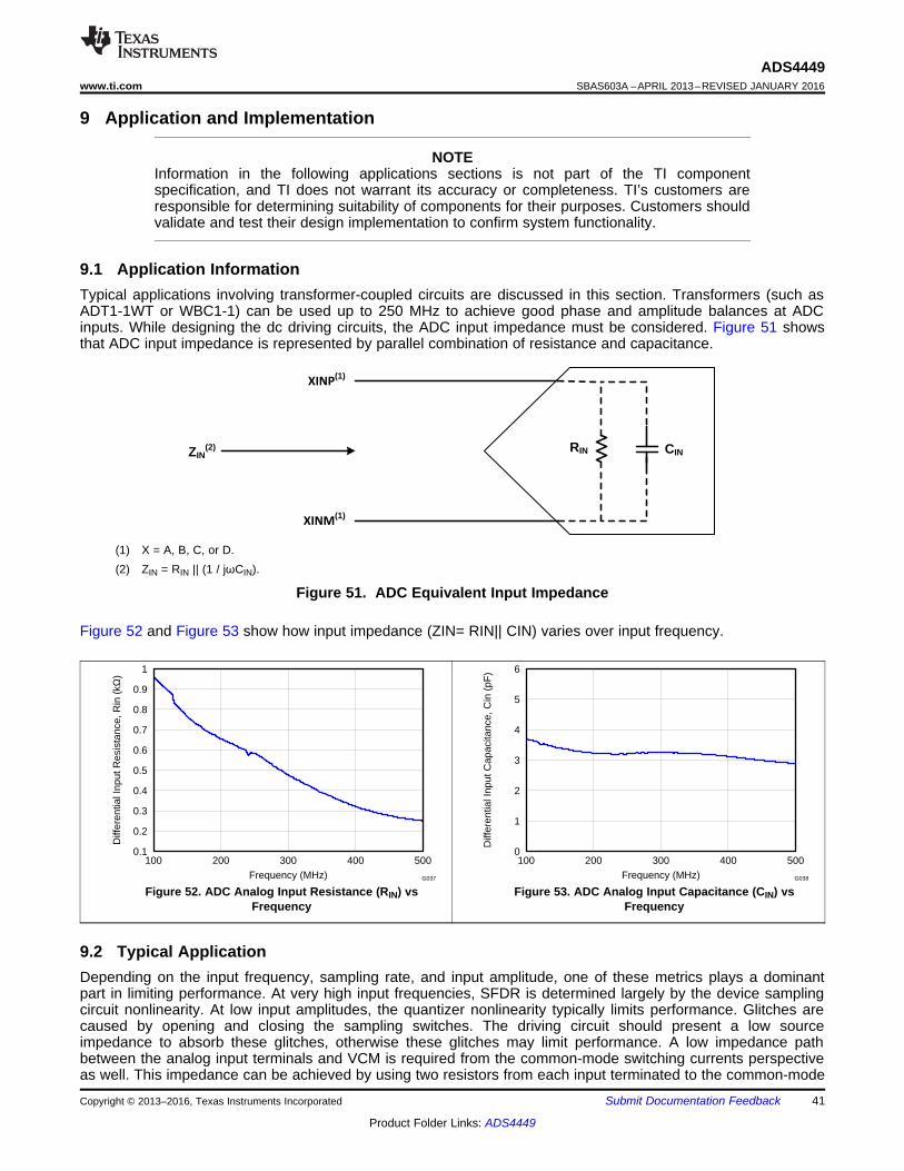
0.1
0.2
0.3
0.4
0.5
0.6
0.7
0.8
0.9
1
100 200 300 400 500Frequency (MHz)
Diff
eren
tial I
nput
Res
ista
nce,
Rin
(kΩ
)
G037
0
1
2
3
4
5
6
100 200 300 400 500Frequency (MHz)
Diff
eren
tial I
nput
Cap
acita
nce,
Cin
(pF
)
G038
XINP(1)
XINM(1)
RINZIN(2) CIN
41
ADS4449www.ti.com SBAS603A –APRIL 2013–REVISED JANUARY 2016
Product Folder Links: ADS4449
Submit Documentation FeedbackCopyright © 2013–2016, Texas Instruments Incorporated
9 Application and Implementation
NOTEInformation in the following applications sections is not part of the TI componentspecification, and TI does not warrant its accuracy or completeness. TI’s customers areresponsible for determining suitability of components for their purposes. Customers shouldvalidate and test their design implementation to confirm system functionality.
9.1 Application InformationTypical applications involving transformer-coupled circuits are discussed in this section. Transformers (such asADT1-1WT or WBC1-1) can be used up to 250 MHz to achieve good phase and amplitude balances at ADCinputs. While designing the dc driving circuits, the ADC input impedance must be considered. Figure 51 showsthat ADC input impedance is represented by parallel combination of resistance and capacitance.
(1) X = A, B, C, or D.(2) ZIN = RIN || (1 / jωCIN).
Figure 51. ADC Equivalent Input Impedance
Figure 52 and Figure 53 show how input impedance (ZIN= RIN|| CIN) varies over input frequency.
Figure 52. ADC Analog Input Resistance (RIN) vsFrequency
Figure 53. ADC Analog Input Capacitance (CIN) vsFrequency
9.2 Typical ApplicationDepending on the input frequency, sampling rate, and input amplitude, one of these metrics plays a dominantpart in limiting performance. At very high input frequencies, SFDR is determined largely by the device samplingcircuit nonlinearity. At low input amplitudes, the quantizer nonlinearity typically limits performance. Glitches arecaused by opening and closing the sampling switches. The driving circuit should present a low sourceimpedance to absorb these glitches, otherwise these glitches may limit performance. A low impedance pathbetween the analog input terminals and VCM is required from the common-mode switching currents perspectiveas well. This impedance can be achieved by using two resistors from each input terminated to the common-mode
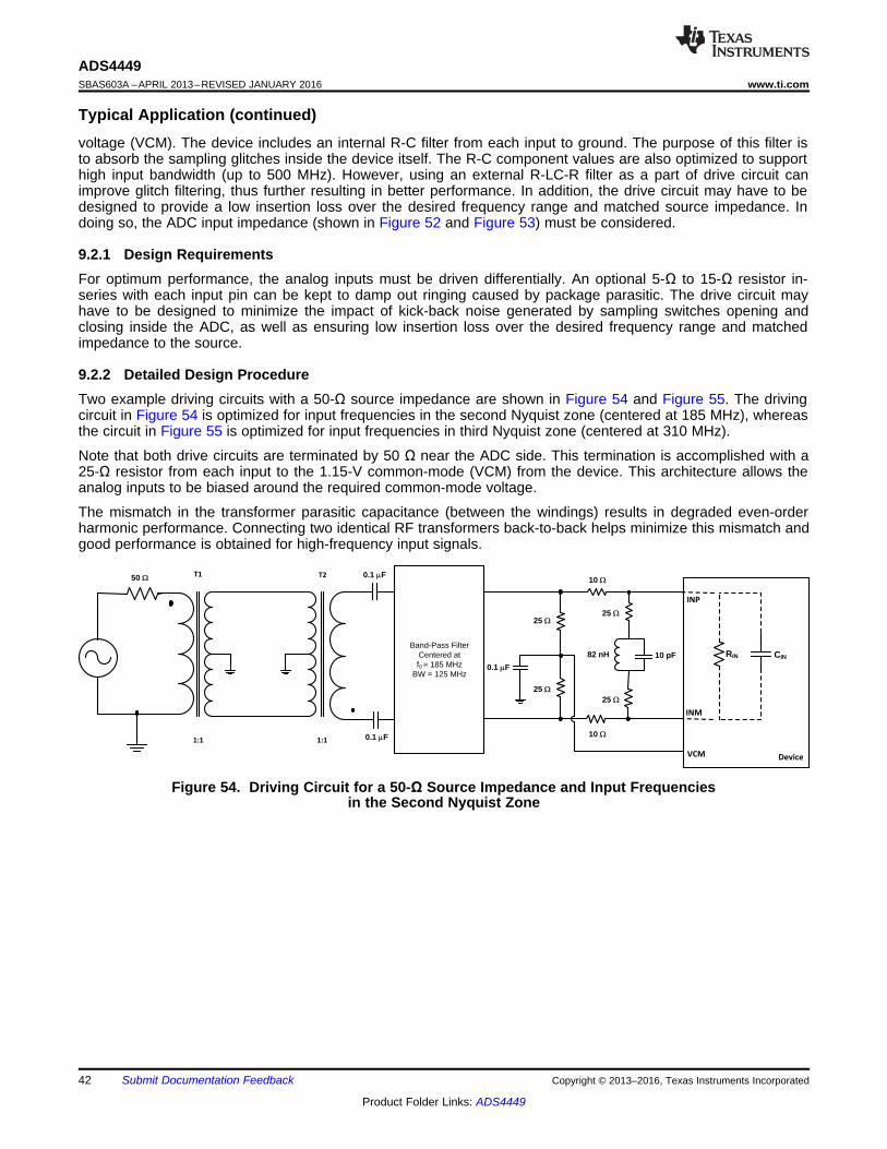
VCMDevice
0.1 PF
25 :
25 :
10 :
10 :
10 pF82 nH
25 :
25 :
INP
INM
RIN CIN
1:1
50 :
1:1
Band-Pass FilterCentered at f0 = 185 MHz
BW = 125 MHz
T1 T2 0.1 PF
0.1 PF
42
ADS4449SBAS603A –APRIL 2013–REVISED JANUARY 2016 www.ti.com
Product Folder Links: ADS4449
Submit Documentation Feedback Copyright © 2013–2016, Texas Instruments Incorporated
Typical Application (continued)voltage (VCM). The device includes an internal R-C filter from each input to ground. The purpose of this filter isto absorb the sampling glitches inside the device itself. The R-C component values are also optimized to supporthigh input bandwidth (up to 500 MHz). However, using an external R-LC-R filter as a part of drive circuit canimprove glitch filtering, thus further resulting in better performance. In addition, the drive circuit may have to bedesigned to provide a low insertion loss over the desired frequency range and matched source impedance. Indoing so, the ADC input impedance (shown in Figure 52 and Figure 53) must be considered.
9.2.1 Design RequirementsFor optimum performance, the analog inputs must be driven differentially. An optional 5-Ω to 15-Ω resistor in-series with each input pin can be kept to damp out ringing caused by package parasitic. The drive circuit mayhave to be designed to minimize the impact of kick-back noise generated by sampling switches opening andclosing inside the ADC, as well as ensuring low insertion loss over the desired frequency range and matchedimpedance to the source.
9.2.2 Detailed Design ProcedureTwo example driving circuits with a 50-Ω source impedance are shown in Figure 54 and Figure 55. The drivingcircuit in Figure 54 is optimized for input frequencies in the second Nyquist zone (centered at 185 MHz), whereasthe circuit in Figure 55 is optimized for input frequencies in third Nyquist zone (centered at 310 MHz).
Note that both drive circuits are terminated by 50 Ω near the ADC side. This termination is accomplished with a25-Ω resistor from each input to the 1.15-V common-mode (VCM) from the device. This architecture allows theanalog inputs to be biased around the required common-mode voltage.
The mismatch in the transformer parasitic capacitance (between the windings) results in degraded even-orderharmonic performance. Connecting two identical RF transformers back-to-back helps minimize this mismatch andgood performance is obtained for high-frequency input signals.
Figure 54. Driving Circuit for a 50-Ω Source Impedance and Input Frequenciesin the Second Nyquist Zone
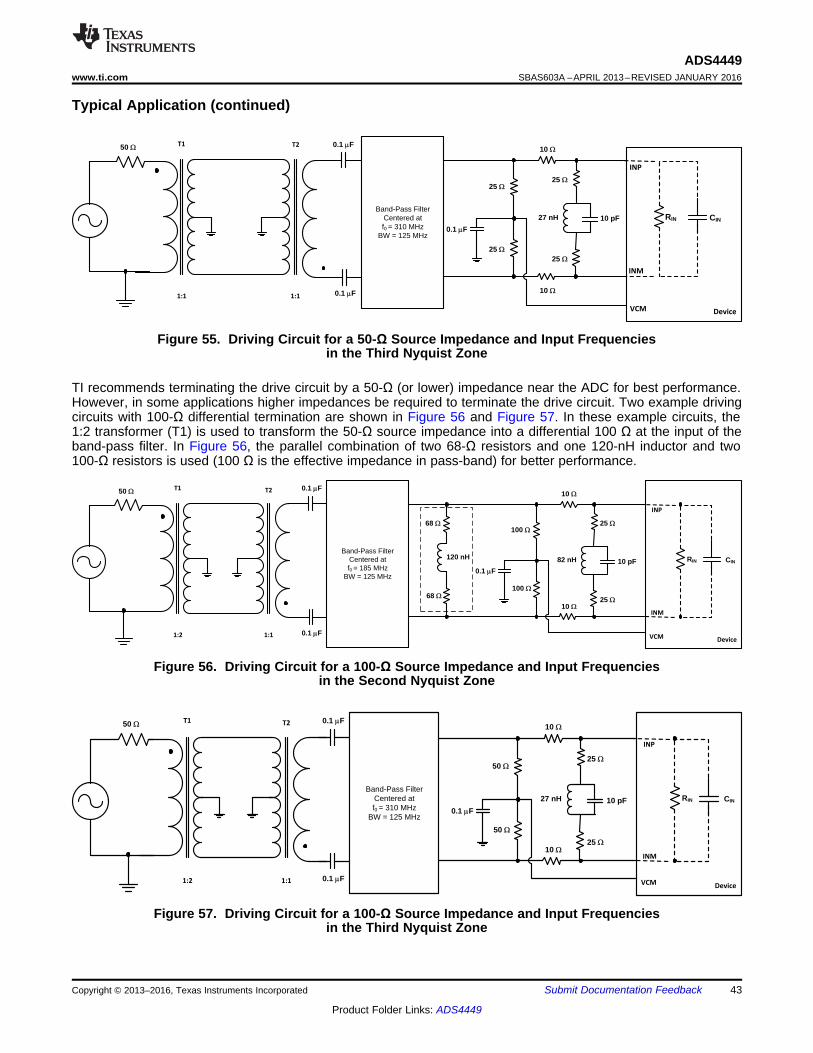
1:2
50 :
1:1
Band-Pass FilterCentered at f0 = 310 MHz
BW = 125 MHz
T1 T2
VCMDevice
0.1 PF
50 :
50 :
10 :
10 :
10 pF27 nH
25 :
25 :
0.1 PF
0.1 PF
INP
INM
RIN CIN
1:2
50 :
1:1
Band-Pass FilterCentered at f0 = 185 MHz
BW = 125 MHz
T1 T2
VCMDevice
0.1 PF
100 :
100 :
10 :
10 :
10 pF82 nH
25 :
25 :
68 :
68 :
120 nH
0.1 PF
0.1 PF
INP
INM
RIN CIN
VCMDevice
0.1 PF
25 :
25 :
10 :
10 :
10 pF27 nH
25 :
25 :
INP
INM
RIN CIN
1:1
50 :
1:1
Band-Pass FilterCentered at f0 = 310 MHz
BW = 125 MHz
T1 T2 0.1 PF
0.1 PF
43
ADS4449www.ti.com SBAS603A –APRIL 2013–REVISED JANUARY 2016
Product Folder Links: ADS4449
Submit Documentation FeedbackCopyright © 2013–2016, Texas Instruments Incorporated
Typical Application (continued)
Figure 55. Driving Circuit for a 50-Ω Source Impedance and Input Frequenciesin the Third Nyquist Zone
TI recommends terminating the drive circuit by a 50-Ω (or lower) impedance near the ADC for best performance.However, in some applications higher impedances be required to terminate the drive circuit. Two example drivingcircuits with 100-Ω differential termination are shown in Figure 56 and Figure 57. In these example circuits, the1:2 transformer (T1) is used to transform the 50-Ω source impedance into a differential 100 Ω at the input of theband-pass filter. In Figure 56, the parallel combination of two 68-Ω resistors and one 120-nH inductor and two100-Ω resistors is used (100 Ω is the effective impedance in pass-band) for better performance.
Figure 56. Driving Circuit for a 100-Ω Source Impedance and Input Frequenciesin the Second Nyquist Zone
Figure 57. Driving Circuit for a 100-Ω Source Impedance and Input Frequenciesin the Third Nyquist Zone

−120
−100
−80
−60
−40
−20
0
0 25 50 75 100 125Frequency (MHz)
Am
plitu
de (
dB)
G005
−120
−100
−80
−60
−40
−20
0
0 25 50 75 100 125Frequency (MHz)
Am
plitu
de (
dB)
G006
44
ADS4449SBAS603A –APRIL 2013–REVISED JANUARY 2016 www.ti.com
Product Folder Links: ADS4449
Submit Documentation Feedback Copyright © 2013–2016, Texas Instruments Incorporated
Typical Application (continued)9.2.3 Application CurvesFigure 10 and Figure 11 below show performance obtained at 170-MHz and 230-MHz input frequenciesrespectively using appropriate driving circuit.
Figure 58. FFT For 170-MHz Input Signal Figure 59. FFT For 230MHz Input Signal
9.2.4 Enabling 14-Bit ResolutionBy default after reset, the device outputs 11-bit data on the Dxx13P, Dxx13M and Dxx3P, Dxx3M terminals andOVR information on the Dxx0P, Dxx0M terminals. When the ALWAYS WRITE 1 bits are set, the ADC outputs13-bit data on the Dxx13P, Dxx13M and Dxx1P, Dxx1M terminals and OVR information on the Dxx0P, Dxx0Mterminals. To enable 14-bit resolution, the DIS OVR ON LSB register bit must be set to 1 as indicated in Table 6.
Table 6. ADC Configuration
ADC TERMINALNAMES
DATA ON ADC TERMINALS
AFTER RESET ALWAYS WRITE 1 = 1 ALWAYS WRITE 1 = 1DIS OVR ON LSB = 1
Dxx13 D13 D13 D13— — — —
Dxx3 D3 D3 D3Dxx2 Logic 0 D2 D2Dxx1 Logic 1 D1 D1Dxx0 OVR OVR D0
Comments 11-bit data (D[13:3]) and OVR comeon ADC output terminals
13-bit data (D[13:1]) and OVR comeon ADC output terminals
14-bit data comes on ADC outputterminals
9.2.5 Analog InputThe analog input consists of a switched-capacitor-based differential sample-and-hold architecture. Thisdifferential topology results in very good ac performance even for high input frequencies at high samplingrates.The INP and INM terminals must be externally biased around a common-mode voltage of 1.15 V, availableon the VCM terminal. For a full-scale differential input, each input terminal (INP, INM) must swingsymmetrically between VCM + 0.5 V and VCM – 0.5 V, resulting in a 2-VPP differential input swing.The input sampling circuit has a high 3-dB bandwidth that extends up to 500 MHz when a 50-Ω source drivesthe ADC analog inputs.
9.2.6 Drive Circuit RequirementsThis configuration improves the common-mode noise immunity and even-order harmonic rejection. A 5-Ω to 15-Ωresistor in series with each input terminal is recommended to damp out ringing caused by package parasitics.

45
ADS4449www.ti.com SBAS603A –APRIL 2013–REVISED JANUARY 2016
Product Folder Links: ADS4449
Submit Documentation FeedbackCopyright © 2013–2016, Texas Instruments Incorporated
Glitches are caused by opening and closing the sampling switches. The driving circuit should present a lowsource impedance to absorb these glitches, otherwise these glitches may limit performance. A low impedancepath between the analog input terminals and VCM is required from the common-mode switching currentsperspective as well. This impedance can be achieved by using two resistors from each input terminated to thecommon-mode voltage (VCM).
The device includes an internal R-C filter from each input to ground. The purpose of this filter is to absorb thesampling glitches inside the device itself. The R-C component values are also optimized to support high inputbandwidth (up to 500 MHz). However, using an external R-LC-R filter (refer to Figure 54, Figure 55, Figure 56,Figure 57, and Figure 60) improves glitch filtering, thus further resulting in better performance.
In addition, the drive circuit may have to be designed to provide a low insertion loss over the desired frequencyrange and matched source impedance. In doing so, the ADC input impedance must be considered. Figure 51,Figure 52, and Figure 53 show the impedance (ZIN = RIN || CIN) at the ADC input terminals.
Spurious-free dynamic range (SFDR) performance can be limited because of several reasons (such as the effectof sampling glitches, sampling circuit nonlinearity, and quantizer nonlinearity that follows the sampling circuit).Depending on the input frequency, sampling rate, and input amplitude, one of these metrics plays a dominantpart in limiting performance. At very high input frequencies, SFDR is determined largely by the device samplingcircuit nonlinearity. At low input amplitudes, the quantizer nonlinearity typically limits performance.
9.2.7 Clock InputThe device clock inputs can be driven differentially with a sine, LVPECL, or LVDS source with little or nodifference in performance between them. The common-mode voltage of the clock inputs is set to 0.95 V usinginternal 5-kΩ resistors, as shown in Figure 60. This setting allows the use of transformer-coupled drive circuits forsine-wave clock or ac-coupling for LVPECL, LVDS, and LVCMOS clock sources (see Figure 61, Figure 62, andFigure 63).
For best performance, the clock inputs must be driven differentially, thereby reducing susceptibility to common-mode noise. TI recommends keeping the differential voltage between clock inputs less than 1.8 VPP to obtainbest performance. A clock source with very low jitter is recommended for high input frequency sampling. Band-pass filtering of the clock source can help reduce the effects of jitter. With a non-50% duty cycle clock input,performance does not change.

0.1 Fm
0.1 Fm
CLKP
CLKM
150 W
150 W
Typical LVPECLClock Input
ZO
ZO
100 W
CLKP
CLKM
0.1 Fm
0.1 Fm
DifferentialSine-WaveClock Input
RT
CLKP
5 kΩ
0.95V
5 kΩ
20 Ω
20 Ω
LPKG
~ 2 nH
CBOND
~ 1 pF
LPKG
~ 2 nH
RESR
~ 100 Ω
RESR
~ 100 Ω
CLKM
Clock Buffer
CEQ CEQCBOND
~ 1 pF
46
ADS4449SBAS603A –APRIL 2013–REVISED JANUARY 2016 www.ti.com
Product Folder Links: ADS4449
Submit Documentation Feedback Copyright © 2013–2016, Texas Instruments Incorporated
NOTE: CEQ is 1 pF to 3 pF and is the equivalent input capacitance of the clock buffer.
Figure 60. Internal Clock Buffer
(1) RT is the termination resistor (optional).
Figure 61. Differential Sine-Wave Clock Driving Circuit
Figure 62. LVPECL Clock Driving Circuit
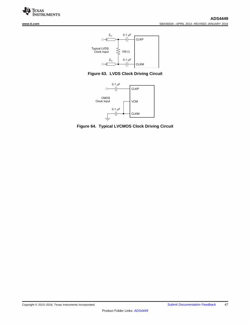
0.1 Fm
0.1 Fm
CLKP
CLKM
CMOSClock Input VCM
0.1 Fm
0.1 Fm
CLKP
CLKM
100 WTypical LVDS
Clock Input
ZO
ZO
47
ADS4449www.ti.com SBAS603A –APRIL 2013–REVISED JANUARY 2016
Product Folder Links: ADS4449
Submit Documentation FeedbackCopyright © 2013–2016, Texas Instruments Incorporated
Figure 63. LVDS Clock Driving Circuit
Figure 64. Typical LVCMOS Clock Driving Circuit
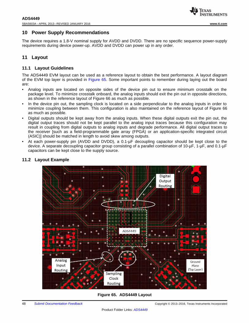
48
ADS4449SBAS603A –APRIL 2013–REVISED JANUARY 2016 www.ti.com
Product Folder Links: ADS4449
Submit Documentation Feedback Copyright © 2013–2016, Texas Instruments Incorporated
10 Power Supply RecommendationsThe device requires a 1.8-V nominal supply for AVDD and DVDD. There are no specific sequence power-supplyrequirements during device power-up. AVDD and DVDD can power up in any order.
11 Layout
11.1 Layout GuidelinesThe ADS4449 EVM layout can be used as a reference layout to obtain the best performance. A layout diagramof the EVM top layer is provided in Figure 65. Some important points to remember during laying out the boardare:• Analog inputs are located on opposite sides of the device pin out to ensure minimum crosstalk on the
package level. To minimize crosstalk onboard, the analog inputs should exit the pin out in opposite directions,as shown in the reference layout of Figure 66 as much as possible.
• In the device pin out, the sampling clock is located on a side perpendicular to the analog inputs in order tominimize coupling between them. This configuration is also maintained on the reference layout of Figure 66as much as possible.
• Digital outputs should be kept away from the analog inputs. When these digital outputs exit the pin out, thedigital output traces should not be kept parallel to the analog input traces because this configuration mayresult in coupling from digital outputs to analog inputs and degrade performance. All digital output traces tothe receiver [such as a field-programmable gate array (FPGA) or an application-specific integrated circuit(ASIC)] should be matched in length to avoid skew among outputs.
• At each power-supply pin (AVDD and DVDD), a 0.1-µF decoupling capacitor should be kept close to thedevice. A separate decoupling capacitor group consisting of a parallel combination of 10-µF, 1-µF, and 0.1-µFcapacitors can be kept close to the supply source.
11.2 Layout Example
Figure 65. ADS4449 Layout
10 S
N D
PSINAD = 10Log
P + P
10 S
N
PSNR = 10Log
P
49
ADS4449www.ti.com SBAS603A –APRIL 2013–REVISED JANUARY 2016
Product Folder Links: ADS4449
Submit Documentation FeedbackCopyright © 2013–2016, Texas Instruments Incorporated
12 Device and Documentation Support
12.1 Device NomenclatureAnalog BandwidthThe analog input frequency at which the power of the fundamental is reduced by 3 dB with
respect to the low-frequency value.
Aperture Delay The delay in time between the rising edge of the input sampling clock and the actual time atwhich the sampling occurs. This delay is different across channels. The maximum variation isspecified as an aperture delay variation (channel-to-channel).
Aperture Uncertainty (Jitter) The sample-to-sample variation in aperture delay.
Clock Pulse Width and Duty Cycle The duty cycle of a clock signal is the ratio of the time the clock signalremains at a logic high (clock pulse width) to the period of the clock signal. Duty cycle is typicallyexpressed as a percentage. A perfect differential sine-wave clock results in a 50% duty cycle.
Maximum Conversion Rate The maximum sampling rate at which specified operation is given. All parametrictesting is performed at this sampling rate, unless otherwise noted.
Minimum Conversion Rate The minimum sampling rate at which the ADC functions.
Differential Nonlinearity (DNL) An ideal ADC exhibits code transitions at analog input values spaced exactly 1LSB apart. DNL is the deviation of any single step from this ideal value, measured in units of LSBs.
Integral Nonlinearity (INL) INL is the deviation of the ADC transfer function from a best-fit line determined by aleast-squares curve fit of that transfer function, measured in units of LSBs.
Gain Error Gain error is the deviation of the ADC actual input full-scale range from the ideal value. Gain erroris given as a percentage of the ideal input full-scale range. Gain error has two components: error asa result of reference inaccuracy and error as a result of the channel. Both errors are specifiedindependently as EGREF and EGCHAN.
To a first-order approximation, the total gain error of ETOTAL is approximately EGREF +EGCHAN.For example, if ETOTAL = ±0.5%, the full-scale input varies from (1 – 0.5 / 100) × fS ideal to (1 +0.5 / 100) × fS ideal.
Offset Error Offset error is the difference, given in number of LSBs, between the ADC actual average idlechannel output code and the ideal average idle channel output code. This quantity is often mappedinto millivolts.
Temperature DriftThe temperature drift coefficient (with respect to gain error and offset error) specifies thechange per degree Celsius of the parameter from TMIN to TMAX. The coefficient is calculated bydividing the maximum deviation of the parameter across the TMIN to TMAX range by the difference ofTMAX – TMIN.
Signal-to-Noise Ratio (SNR) SNR is the ratio of the power of the fundamental (PS) to the noise floor power(PN), excluding the power at dc and the first nine harmonics.
(1)SNR is either given in units of dBc (dB to carrier) when the absolute power of thefundamental is used as the reference, or dBFS (dB to full-scale) when the power of thefundamental is extrapolated to the converter full-scale range.
Signal-to-Noise and Distortion (SINAD) SINAD is the ratio of the power of the fundamental (PS) to the powerof all other spectral components, including noise (PN) and distortion (PD) but excluding dc.
(2)SINAD is either given in units of dBc (dB to carrier) when the absolute power of thefundamental is used as the reference, or dBFS (dB to full-scale) when the power of thefundamental is extrapolated to the converter full-scale range.

50
ADS4449SBAS603A –APRIL 2013–REVISED JANUARY 2016 www.ti.com
Product Folder Links: ADS4449
Submit Documentation Feedback Copyright © 2013–2016, Texas Instruments Incorporated
12.2 Documentation Support
12.2.1 Related DocumentationFor related documentation see the following:• ADS4449 User Guide, SLAU485• Design Considerations for Avoiding Timing Errors during High-Speed ADC, LVDS Data Interface with FPGA,
SLAA592• Why Oversample when Undersampling can do the Job?, SLAA594
12.3 Community ResourcesThe following links connect to TI community resources. Linked contents are provided "AS IS" by the respectivecontributors. They do not constitute TI specifications and do not necessarily reflect TI's views; see TI's Terms ofUse.
TI E2E™ Online Community TI's Engineer-to-Engineer (E2E) Community. Created to foster collaborationamong engineers. At e2e.ti.com, you can ask questions, share knowledge, explore ideas and helpsolve problems with fellow engineers.
Design Support TI's Design Support Quickly find helpful E2E forums along with design support tools andcontact information for technical support.
12.4 TrademarksE2E is a trademark of Texas Instruments.All other trademarks are the property of their respective owners.
12.5 Electrostatic Discharge CautionThese devices have limited built-in ESD protection. The leads should be shorted together or the device placed in conductive foamduring storage or handling to prevent electrostatic damage to the MOS gates.
12.6 GlossarySLYZ022 — TI Glossary.
This glossary lists and explains terms, acronyms, and definitions.
13 Mechanical, Packaging, and Orderable InformationThe following pages include mechanical, packaging, and orderable information. This information is the mostcurrent data available for the designated devices. This data is subject to change without notice and revision ofthis document. For browser-based versions of this data sheet, refer to the left-hand navigation.
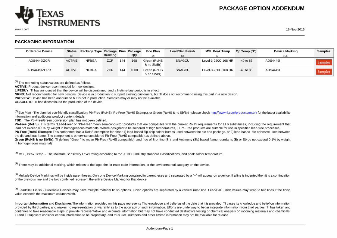
PACKAGE OPTION ADDENDUM
www.ti.com 16-Nov-2016
Addendum-Page 1
PACKAGING INFORMATION
Orderable Device Status(1)
Package Type PackageDrawing
Pins PackageQty
Eco Plan(2)
Lead/Ball Finish(6)
MSL Peak Temp(3)
Op Temp (°C) Device Marking(4/5)
Samples
ADS4449IZCR ACTIVE NFBGA ZCR 144 168 Green (RoHS& no Sb/Br)
SNAGCU Level-3-260C-168 HR -40 to 85 ADS4449I
ADS4449IZCRR ACTIVE NFBGA ZCR 144 1000 Green (RoHS& no Sb/Br)
SNAGCU Level-3-260C-168 HR -40 to 85 ADS4449I
(1) The marketing status values are defined as follows:ACTIVE: Product device recommended for new designs.LIFEBUY: TI has announced that the device will be discontinued, and a lifetime-buy period is in effect.NRND: Not recommended for new designs. Device is in production to support existing customers, but TI does not recommend using this part in a new design.PREVIEW: Device has been announced but is not in production. Samples may or may not be available.OBSOLETE: TI has discontinued the production of the device.
(2) Eco Plan - The planned eco-friendly classification: Pb-Free (RoHS), Pb-Free (RoHS Exempt), or Green (RoHS & no Sb/Br) - please check http://www.ti.com/productcontent for the latest availabilityinformation and additional product content details.TBD: The Pb-Free/Green conversion plan has not been defined.Pb-Free (RoHS): TI's terms "Lead-Free" or "Pb-Free" mean semiconductor products that are compatible with the current RoHS requirements for all 6 substances, including the requirement thatlead not exceed 0.1% by weight in homogeneous materials. Where designed to be soldered at high temperatures, TI Pb-Free products are suitable for use in specified lead-free processes.Pb-Free (RoHS Exempt): This component has a RoHS exemption for either 1) lead-based flip-chip solder bumps used between the die and package, or 2) lead-based die adhesive used betweenthe die and leadframe. The component is otherwise considered Pb-Free (RoHS compatible) as defined above.Green (RoHS & no Sb/Br): TI defines "Green" to mean Pb-Free (RoHS compatible), and free of Bromine (Br) and Antimony (Sb) based flame retardants (Br or Sb do not exceed 0.1% by weightin homogeneous material)
(3) MSL, Peak Temp. - The Moisture Sensitivity Level rating according to the JEDEC industry standard classifications, and peak solder temperature.
(4) There may be additional marking, which relates to the logo, the lot trace code information, or the environmental category on the device.
(5) Multiple Device Markings will be inside parentheses. Only one Device Marking contained in parentheses and separated by a "~" will appear on a device. If a line is indented then it is a continuationof the previous line and the two combined represent the entire Device Marking for that device.
(6) Lead/Ball Finish - Orderable Devices may have multiple material finish options. Finish options are separated by a vertical ruled line. Lead/Ball Finish values may wrap to two lines if the finishvalue exceeds the maximum column width.
Important Information and Disclaimer:The information provided on this page represents TI's knowledge and belief as of the date that it is provided. TI bases its knowledge and belief on informationprovided by third parties, and makes no representation or warranty as to the accuracy of such information. Efforts are underway to better integrate information from third parties. TI has taken andcontinues to take reasonable steps to provide representative and accurate information but may not have conducted destructive testing or chemical analysis on incoming materials and chemicals.TI and TI suppliers consider certain information to be proprietary, and thus CAS numbers and other limited information may not be available for release.

PACKAGE OPTION ADDENDUM
www.ti.com 16-Nov-2016
Addendum-Page 2
In no event shall TI's liability arising out of such information exceed the total purchase price of the TI part(s) at issue in this document sold by TI to Customer on an annual basis.
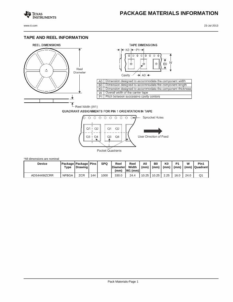
TAPE AND REEL INFORMATION
*All dimensions are nominal
Device PackageType
PackageDrawing
Pins SPQ ReelDiameter
(mm)
ReelWidth
W1 (mm)
A0(mm)
B0(mm)
K0(mm)
P1(mm)
W(mm)
Pin1Quadrant
ADS4449IZCRR NFBGA ZCR 144 1000 330.0 24.4 10.25 10.25 2.25 16.0 24.0 Q1
PACKAGE MATERIALS INFORMATION
www.ti.com 23-Jul-2013
Pack Materials-Page 1

*All dimensions are nominal
Device Package Type Package Drawing Pins SPQ Length (mm) Width (mm) Height (mm)
ADS4449IZCRR NFBGA ZCR 144 1000 336.6 336.6 31.8
PACKAGE MATERIALS INFORMATION
www.ti.com 23-Jul-2013
Pack Materials-Page 2

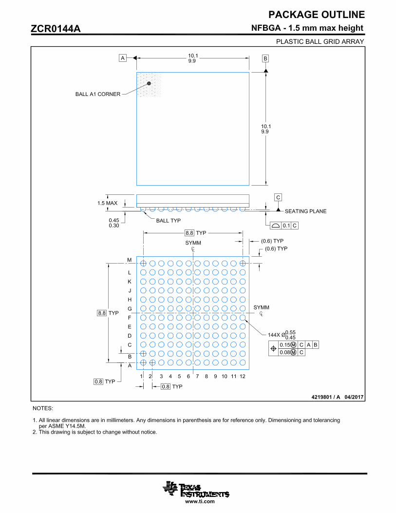
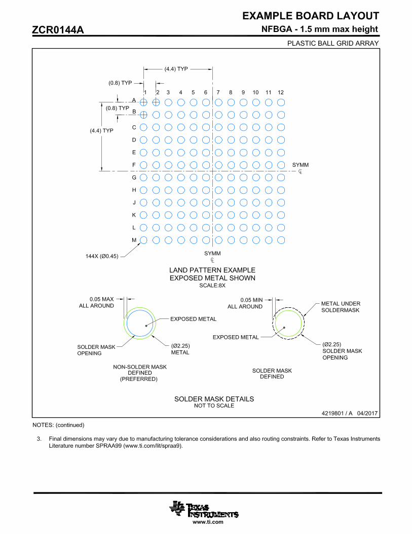
IMPORTANT NOTICE
Texas Instruments Incorporated (TI) reserves the right to make corrections, enhancements, improvements and other changes to itssemiconductor products and services per JESD46, latest issue, and to discontinue any product or service per JESD48, latest issue. Buyersshould obtain the latest relevant information before placing orders and should verify that such information is current and complete.TI’s published terms of sale for semiconductor products (http://www.ti.com/sc/docs/stdterms.htm) apply to the sale of packaged integratedcircuit products that TI has qualified and released to market. Additional terms may apply to the use or sale of other types of TI products andservices.Reproduction of significant portions of TI information in TI data sheets is permissible only if reproduction is without alteration and isaccompanied by all associated warranties, conditions, limitations, and notices. TI is not responsible or liable for such reproduceddocumentation. Information of third parties may be subject to additional restrictions. Resale of TI products or services with statementsdifferent from or beyond the parameters stated by TI for that product or service voids all express and any implied warranties for theassociated TI product or service and is an unfair and deceptive business practice. TI is not responsible or liable for any such statements.Buyers and others who are developing systems that incorporate TI products (collectively, “Designers”) understand and agree that Designersremain responsible for using their independent analysis, evaluation and judgment in designing their applications and that Designers havefull and exclusive responsibility to assure the safety of Designers' applications and compliance of their applications (and of all TI productsused in or for Designers’ applications) with all applicable regulations, laws and other applicable requirements. Designer represents that, withrespect to their applications, Designer has all the necessary expertise to create and implement safeguards that (1) anticipate dangerousconsequences of failures, (2) monitor failures and their consequences, and (3) lessen the likelihood of failures that might cause harm andtake appropriate actions. Designer agrees that prior to using or distributing any applications that include TI products, Designer willthoroughly test such applications and the functionality of such TI products as used in such applications.TI’s provision of technical, application or other design advice, quality characterization, reliability data or other services or information,including, but not limited to, reference designs and materials relating to evaluation modules, (collectively, “TI Resources”) are intended toassist designers who are developing applications that incorporate TI products; by downloading, accessing or using TI Resources in anyway, Designer (individually or, if Designer is acting on behalf of a company, Designer’s company) agrees to use any particular TI Resourcesolely for this purpose and subject to the terms of this Notice.TI’s provision of TI Resources does not expand or otherwise alter TI’s applicable published warranties or warranty disclaimers for TIproducts, and no additional obligations or liabilities arise from TI providing such TI Resources. TI reserves the right to make corrections,enhancements, improvements and other changes to its TI Resources. TI has not conducted any testing other than that specificallydescribed in the published documentation for a particular TI Resource.Designer is authorized to use, copy and modify any individual TI Resource only in connection with the development of applications thatinclude the TI product(s) identified in such TI Resource. NO OTHER LICENSE, EXPRESS OR IMPLIED, BY ESTOPPEL OR OTHERWISETO ANY OTHER TI INTELLECTUAL PROPERTY RIGHT, AND NO LICENSE TO ANY TECHNOLOGY OR INTELLECTUAL PROPERTYRIGHT OF TI OR ANY THIRD PARTY IS GRANTED HEREIN, including but not limited to any patent right, copyright, mask work right, orother intellectual property right relating to any combination, machine, or process in which TI products or services are used. Informationregarding or referencing third-party products or services does not constitute a license to use such products or services, or a warranty orendorsement thereof. Use of TI Resources may require a license from a third party under the patents or other intellectual property of thethird party, or a license from TI under the patents or other intellectual property of TI.TI RESOURCES ARE PROVIDED “AS IS” AND WITH ALL FAULTS. TI DISCLAIMS ALL OTHER WARRANTIES ORREPRESENTATIONS, EXPRESS OR IMPLIED, REGARDING RESOURCES OR USE THEREOF, INCLUDING BUT NOT LIMITED TOACCURACY OR COMPLETENESS, TITLE, ANY EPIDEMIC FAILURE WARRANTY AND ANY IMPLIED WARRANTIES OFMERCHANTABILITY, FITNESS FOR A PARTICULAR PURPOSE, AND NON-INFRINGEMENT OF ANY THIRD PARTY INTELLECTUALPROPERTY RIGHTS. TI SHALL NOT BE LIABLE FOR AND SHALL NOT DEFEND OR INDEMNIFY DESIGNER AGAINST ANY CLAIM,INCLUDING BUT NOT LIMITED TO ANY INFRINGEMENT CLAIM THAT RELATES TO OR IS BASED ON ANY COMBINATION OFPRODUCTS EVEN IF DESCRIBED IN TI RESOURCES OR OTHERWISE. IN NO EVENT SHALL TI BE LIABLE FOR ANY ACTUAL,DIRECT, SPECIAL, COLLATERAL, INDIRECT, PUNITIVE, INCIDENTAL, CONSEQUENTIAL OR EXEMPLARY DAMAGES INCONNECTION WITH OR ARISING OUT OF TI RESOURCES OR USE THEREOF, AND REGARDLESS OF WHETHER TI HAS BEENADVISED OF THE POSSIBILITY OF SUCH DAMAGES.Unless TI has explicitly designated an individual product as meeting the requirements of a particular industry standard (e.g., ISO/TS 16949and ISO 26262), TI is not responsible for any failure to meet such industry standard requirements.Where TI specifically promotes products as facilitating functional safety or as compliant with industry functional safety standards, suchproducts are intended to help enable customers to design and create their own applications that meet applicable functional safety standardsand requirements. Using products in an application does not by itself establish any safety features in the application. Designers mustensure compliance with safety-related requirements and standards applicable to their applications. Designer may not use any TI products inlife-critical medical equipment unless authorized officers of the parties have executed a special contract specifically governing such use.Life-critical medical equipment is medical equipment where failure of such equipment would cause serious bodily injury or death (e.g., lifesupport, pacemakers, defibrillators, heart pumps, neurostimulators, and implantables). Such equipment includes, without limitation, allmedical devices identified by the U.S. Food and Drug Administration as Class III devices and equivalent classifications outside the U.S.TI may expressly designate certain products as completing a particular qualification (e.g., Q100, Military Grade, or Enhanced Product).Designers agree that it has the necessary expertise to select the product with the appropriate qualification designation for their applicationsand that proper product selection is at Designers’ own risk. Designers are solely responsible for compliance with all legal and regulatoryrequirements in connection with such selection.Designer will fully indemnify TI and its representatives against any damages, costs, losses, and/or liabilities arising out of Designer’s non-compliance with the terms and provisions of this Notice.
Mailing Address: Texas Instruments, Post Office Box 655303, Dallas, Texas 75265Copyright © 2018, Texas Instruments Incorporated