Adjustable Current Limited Power Distribution Switch TJ2100htckorea.co.kr/Datasheet/DDR Power...
16
Adjustable Current Limited Power Distribution Switch TJ2100 May. 2014–R1.2 - 1 - HTC FEATURES 105mΩ High-Side MOSFET 2.7V to 5.5V Operating Range Adjustable Current Limit : 200mA to 3.0A(Typ.) ±10% Current-Limit Accuracy at 1.5A(Typ.) Fold-back Short Circuit Protection 90uA Typical On-State Supply Current 1uA Maximum Standby Supply Current Independent Open-drain Fault Flag Pin Thermal Shutdown Protection Under Voltage Lockout(UVLO) TJ2100H : Active High version TJ2100L : Active Low version TJ2100A : Fixed Enable version APPLICATION USB Peripherals General Purpose Power Switching ACPI Power Distribution Notebook PCs PDAs Hot Plug-in Power Supplies DESCRIPSION The TJ2100X is single-channel High-Side MOSFET switch optimized for adjustable current limited power distribution requiring circuit protection. The TJ2100X series support the following USB requirements. The TJ2100 series supply up to 2.5A as required by USB downstream devices. Maximum continuous current can be different on the types of package and ambient temperature. Switch’s low on-resistance meets USB voltage drop requirement. Flag output indicate fault condition to the local USB controller. Soft-start prevents the transient voltage drop on the upstream port that can occur when the switch is enabled in bus-powered applications. Under voltage lockout (UVLO) feature disables the output switches until a valid input voltage. Also the TJ2100 include thermal shutdown to prevent switch failure from high-current loads. SOT23-6L PKG DFN2X2-6L PKG ORDERING INFORMATION Device Package TJ2100HGSF6 SOT23-6L TJ2100LGSF6 TJ2100AGSF6 TJ2100HGQ DFN2X2-6L TJ2100LGQ TJ2100AGQ
-
Upload
nguyenkhuong -
Category
Documents
-
view
218 -
download
0
Transcript of Adjustable Current Limited Power Distribution Switch TJ2100htckorea.co.kr/Datasheet/DDR Power...

Adjustable Current Limited Power Distribution Switch TJ2100
May. 2014–R1.2 - 1 - HTC
FEATURES
105mΩ High-Side MOSFET
2.7V to 5.5V Operating Range
Adjustable Current Limit : 200mA to 3.0A(Typ.)
±10% Current-Limit Accuracy at 1.5A(Typ.)
Fold-back Short Circuit Protection
90uA Typical On-State Supply Current
1uA Maximum Standby Supply Current
Independent Open-drain Fault Flag Pin
Thermal Shutdown Protection
Under Voltage Lockout(UVLO)
TJ2100H : Active High version
TJ2100L : Active Low version
TJ2100A : Fixed Enable version
APPLICATION
USB Peripherals
General Purpose Power Switching
ACPI Power Distribution
Notebook PCs
PDAs
Hot Plug-in Power Supplies
DESCRIPSION
The TJ2100X is single-channel High-Side
MOSFET switch optimized for adjustable current
limited power distribution requiring circuit
protection.
The TJ2100X series support the following USB
requirements. The TJ2100 series supply up to
2.5A as required by USB downstream devices.
Maximum continuous current can be different on
the types of package and ambient temperature.
Switch’s low on-resistance meets USB voltage
drop requirement. Flag output indicate fault
condition to the local USB controller. Soft-start
prevents the transient voltage drop on the
upstream port that can occur when the switch is
enabled in bus-powered applications. Under
voltage lockout (UVLO) feature disables the
output switches until a valid input voltage. Also
the TJ2100 include thermal shutdown to prevent
switch failure from high-current loads.
SOT23-6L PKG
DFN2X2-6L PKG
ORDERING INFORMATION
Device Package
TJ2100HGSF6
SOT23-6L TJ2100LGSF6
TJ2100AGSF6
TJ2100HGQ
DFN2X2-6L TJ2100LGQ
TJ2100AGQ

Adjustable Current Limited Power Distribution Switch TJ2100
May. 2014–R1.2 - 1 - HTC
Absolute Maximum Ratings (Note 1)
Characteristic Symbol Min Max Unit
Supply Voltage VIN -0.3 6.0 V
Enable Input Voltage (Note 2) VEN -0.3 6.0 V
Fault Flag Voltage VFLG - 6.0 V
Fault Flag Current IFLAG - 25 mA
Output Voltage VOUT 6.0 V
Output Current IOUT Internally Limited
Storage Temperature Range TSTG -65 150
Operating Ratings (Note 3),(Note 4)
Characteristic Symbol Min Max Unit
Supply Voltage VIN 2.7 5.5 V
Ambient Temperature Range TA -40 +80
Operating Junction Temperature Range TJ -40 125
Thermal Resistance
Junction-to-Ambient
SOP23-6L (Note 5) θJA 250 oC/W
DFN2x2-6L(Note 6) θJA 165 oC/W
Note:
1. Exceeding the absolute maximum ratings may damage the device.
2. It is recommended for VEN voltage not to exceed VIN voltage.
3. The device is not guaranteed to function outside its operating rating.
4. Devices are ESD sensitive. Handling precautions are recommended.
5. Test Condition for SOT23-6L : Copper Area = 35mm2 , Board Size = 430 mm X 430mm, 1.6T
6. Test Condition for DFN2x2-6L : Copper Area = 35mm2 , Board Size = 430 mm X 430mm, 1.6T

Adjustable Current Limited Power Distribution Switch TJ2100
May. 2014–R1.2 - 2 - HTC
Ordering Information
Package Oder No. Description Marking Compliance Status
SOT23-6L TJ2100LGSF6 Adjustable , Active Low 2100LG RoHS, Green Contact Us
DFN2X2-6L TJ2100LGQ Adjustable , Active Low 2100LG RoHS, Green Contact Us
SOT23-6L TJ2100HGSF6 Adjustable , Active High 2100HG RoHS, Green Contact Us
DFN2X2-6L TJ2100HGQ Adjustable , Active High 2100HG RoHS, Green Contact Us
SOT23-6L TJ2100AGSF6 Adjustable, Fixed Enable 2100AG RoHS, Green Contact Us
DFN2X2-6L TJ2100AGQ Adjustable, Fixed Enable 2100AG RoHS, Green Contact Us
2100TJ
Package Type
Root Name
Product Code
: DFN2X2-6L
Green Mode G Blank
: Halogen Free : Pb Free
Enable ModeHL A
: Active – High
: Active – Low: Fixed Enable
SF6 Q
: SOT23-6L

Adjustable Current Limited Power Distribution Switch TJ2100
May. 2014–R1.2 - 3 - HTC
TYPICAL APPLICATION CIRCUIT
EN
FLG
OUT
GND
IN
VCC
2.7V to 5V
USB
Control
USB
Ports
TJ2100L/H
D+
D-
VBUS
GND
33uF
10uF
VCONT
10K
RILIM
20kΩ
ILIM
1uF
FLG
OUT
GND
IN
VCC
2.7V to 5V
USB
Control
USB
Ports
TJ2100A
D+
D-
VBUS
GND
33uF
10uF
VCONT
10K
RILIM
20kΩ
ILIM1uF
FUNCTION BLOCK DIAGRAM
Current
Limit
Flag
Logic
Thermal
ShutdownUVLO BIAS
Gate
Control
EN / NC
FLG
OUT
IN
ILIM
GND

Adjustable Current Limited Power Distribution Switch TJ2100
May. 2014–R1.2 - 4 - HTC
PIN CONFIGURATION
4
1
3
2
6
SOT-23-6L
IN
EN/NC
OUT
FLG
ILIM 5 GND
DFN2X2-6L
1
3
2
6
4
5GND
EN/NC
IN
ILIM
OUT
FLG
PAD
PIN DESCRIPTION
Pin Name
Pin No.
Pin Description & Function
SOT23-6L DFN2X2-6L
OUT 1 6 Switch Output: Output MOSFET source. Typically connect to
switched side of load.
ILIM 2 5 Current Limit Set. External resistor used to set current limit
threshold.
FLG 3 4 Fault Flag: Active-low, open-drain output. Indicates Short
circuit current, UVLO and Thermal shutdown.
EN / NC 4 3
Enable: Logic-Compatible enable input. (H: active high, L:
active low). Do not float.
NC: No internal connection at fixed enable type. (Note 7)
GND 5 2 Ground
IN 6 1 Supply Input: Output MOSFET drain. Also supplies IC’s
internal circuitry. Connect to positive supply.
Note:
7. The NC pin in TJ2100A is recommended to tie at Ground.
Adjustable Current Limited Power Distribution Switch TJ2100
May. 2014–R1.2 - 5 - HTC
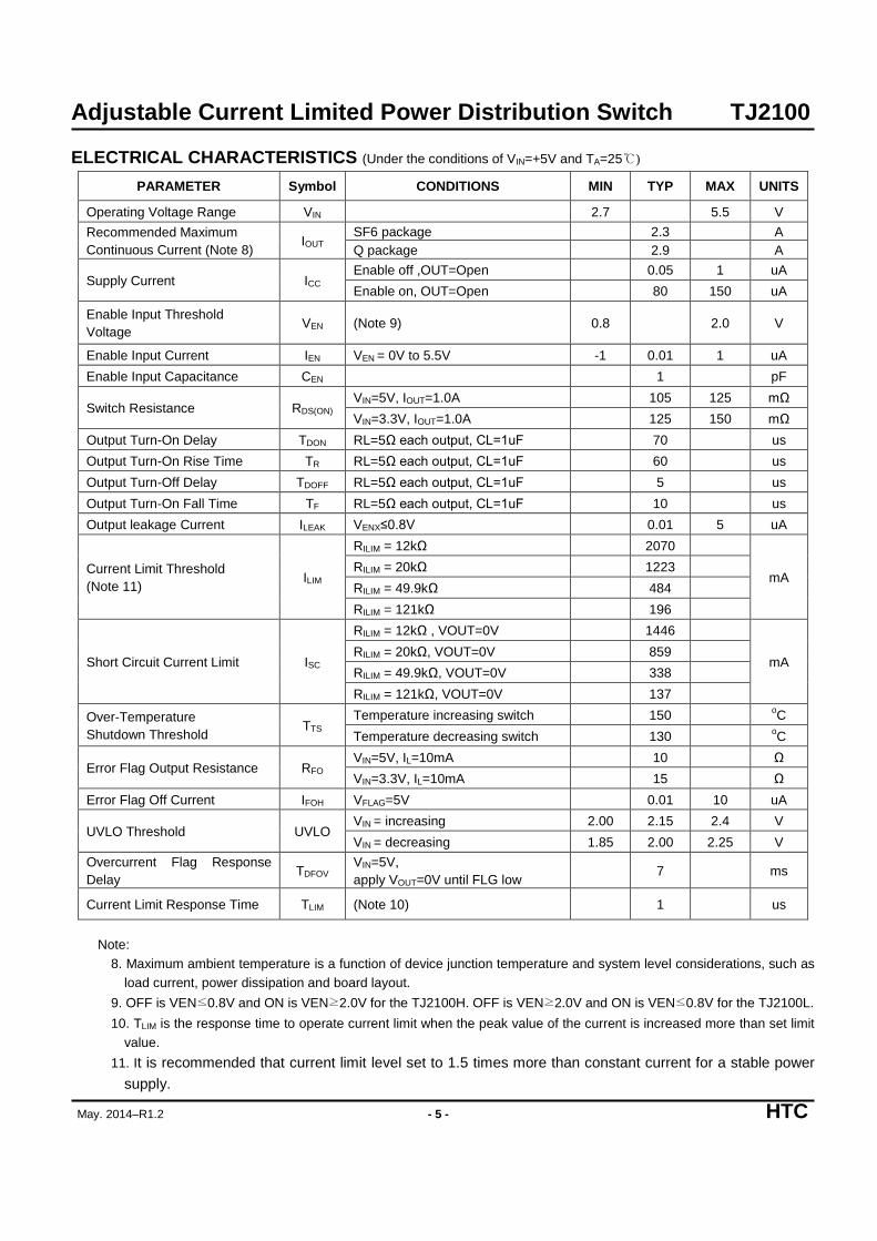
ELECTRICAL CHARACTERISTICS (Under the conditions of VIN=+5V and TA=25)
PARAMETER Symbol CONDITIONS MIN TYP MAX UNITS
Operating Voltage Range VIN 2.7 5.5 V
Recommended Maximum
Continuous Current (Note 8) IOUT
SF6 package 2.3 A
Q package 2.9 A
Supply Current ICC Enable off ,OUT=Open 0.05 1 uA
Enable on, OUT=Open 80 150 uA
Enable Input Threshold
Voltage VEN (Note 9) 0.8 2.0 V
Enable Input Current IEN VEN = 0V to 5.5V -1 0.01 1 uA
Enable Input Capacitance CEN 1 pF
Switch Resistance RDS(ON) VIN=5V, IOUT=1.0A 105 125 mΩ
VIN=3.3V, IOUT=1.0A 125 150 mΩ
Output Turn-On Delay TDON RL=5Ω each output, CL=1uF 70 us
Output Turn-On Rise Time TR RL=5Ω each output, CL=1uF 60 us
Output Turn-Off Delay TDOFF RL=5Ω each output, CL=1uF 5 us
Output Turn-On Fall Time TF RL=5Ω each output, CL=1uF 10 us
Output leakage Current ILEAK VENX≤0.8V 0.01 5 uA
Current Limit Threshold
(Note 11) ILIM
RILIM = 12kΩ 2070
mA RILIM = 20kΩ 1223
RILIM = 49.9kΩ 484
RILIM = 121kΩ 196
Short Circuit Current Limit ISC
RILIM = 12kΩ , VOUT=0V 1446
mA RILIM = 20kΩ, VOUT=0V 859
RILIM = 49.9kΩ, VOUT=0V 338
RILIM = 121kΩ, VOUT=0V 137
Over-Temperature
Shutdown Threshold TTS
Temperature increasing switch 150 oC
Temperature decreasing switch 130 oC
Error Flag Output Resistance RFO VIN=5V, IL=10mA 10 Ω
VIN=3.3V, IL=10mA 15 Ω
Error Flag Off Current IFOH VFLAG=5V 0.01 10 uA
UVLO Threshold UVLO VIN = increasing 2.00 2.15 2.4 V
VIN = decreasing 1.85 2.00 2.25 V
Overcurrent Flag Response
Delay TDFOV
VIN=5V,
apply VOUT=0V until FLG low 7 ms
Current Limit Response Time TLIM (Note 10) 1 us
Note:
8. Maximum ambient temperature is a function of device junction temperature and system level considerations, such as
load current, power dissipation and board layout.
9. OFF is VEN≤0.8V and ON is VEN≥2.0V for the TJ2100H. OFF is VEN≥2.0V and ON is VEN≤0.8V for the TJ2100L.
10. TLIM is the response time to operate current limit when the peak value of the current is increased more than set limit
value.
11. It is recommended that current limit level set to 1.5 times more than constant current for a stable power
supply.

Adjustable Current Limited Power Distribution Switch TJ2100
May. 2014–R1.2 - 6 - HTC
Test Circuit
EN
FLG
OUT
GND
IN
VCCTJ2100L/H
R2 CL
C1
0.1u to 10uFR1
VOUT
10K
RILIM
ILIM
CF (Note 12)
1uF
FLG
OUT
GND
IN
VCCTJ2100A
R2 CL
C1
0.1u to 10uFR1
VOUT
10K
RILIM
ILIMCF (Note 12)
1uF
Note:
12. When the CF should be omitted, it is highly recommended to apply 2.2uF or higher capacitance for C1.
Adjustable Current Limited Power Distribution Switch TJ2100
May. 2014–R1.2 - 7 - HTC
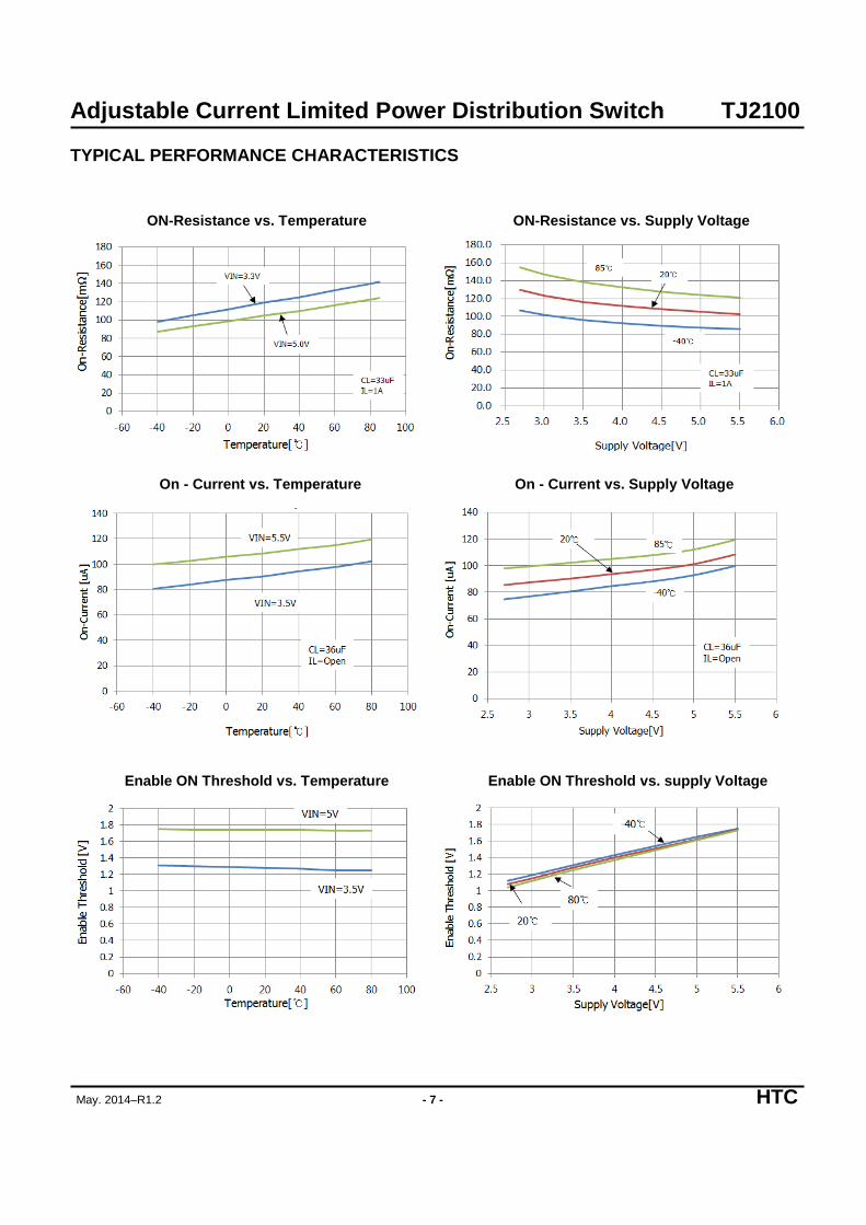
TYPICAL PERFORMANCE CHARACTERISTICS
ON-Resistance vs. Temperature
ON-Resistance vs. Supply Voltage
On - Current vs. Temperature
On - Current vs. Supply Voltage
Enable ON Threshold vs. Temperature
Enable ON Threshold vs. supply Voltage

Adjustable Current Limited Power Distribution Switch TJ2100
May. 2014–R1.2 - 8 - HTC
Enable OFF Threshold vs. Temperature
Enable OFF Threshold vs. supply Voltage
Current Limit Threshold vs. Temperature
Current Limit Threshold vs. Supply Voltage
Short Circuit Current vs. Temperature
Short Circuit Current vs. Supply Voltage
Adjustable Current Limited Power Distribution Switch TJ2100
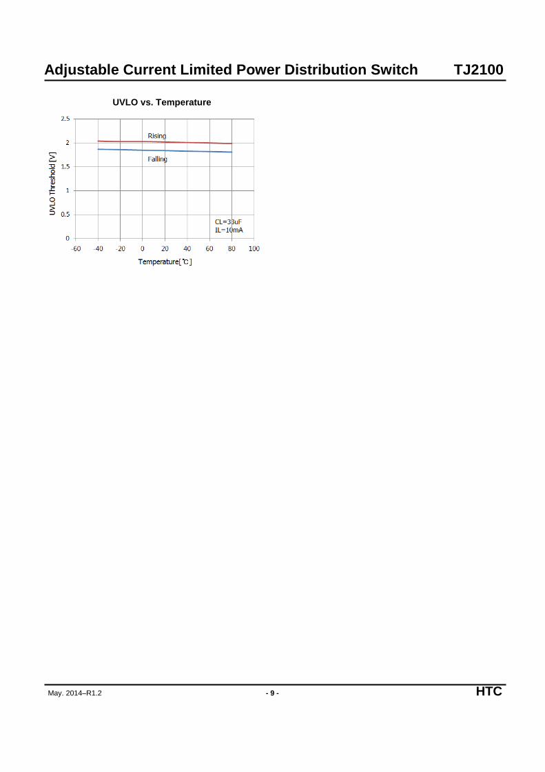
May. 2014–R1.2 - 9 - HTC
UVLO vs. Temperature
Adjustable Current Limited Power Distribution Switch TJ2100
May. 2014–R1.2 - 10 - HTC
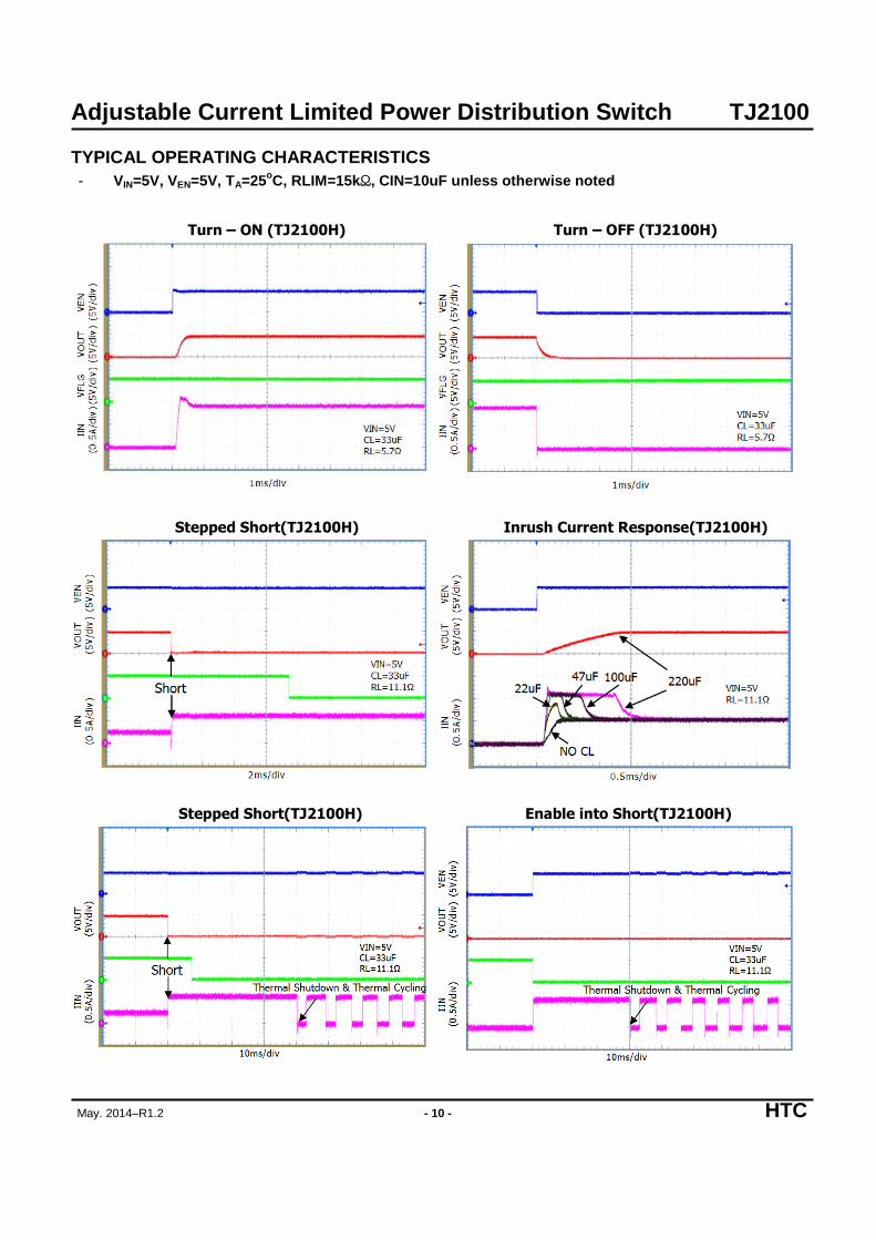
TYPICAL OPERATING CHARACTERISTICS
- VIN=5V, VEN=5V, TA=25oC, RLIM=15kΩ, CIN=10uF unless otherwise noted
Turn – ON (TJ2100H)
Turn – OFF (TJ2100H)
Stepped Short(TJ2100H)
Inrush Current Response(TJ2100H)
Stepped Short(TJ2100H)
Enable into Short(TJ2100H)

Adjustable Current Limited Power Distribution Switch TJ2100
May. 2014–R1.2 - 11 - HTC
UVLO(TJ2100H)
Thermal Shutdown(TJ2100H)

Adjustable Current Limited Power Distribution Switch TJ2100
May. 2014–R1.2 - 12 - HTC
Function Description
Supply Filtering
A 0.1uF to 10uF bypass capacitor from IN pin to GND pin is recommended to control power supply
transients. Recommend X5R or X7R dielectrics when using ceramic capacitors for input/output. Without
this bypass capacitor, an output short can cause ringing from supply lead inductance on the input and
damage the internal control circuitry.
Input or output transients must not exceed the absolute maximum supply voltage (VIN(MAX) = 6V).
Power Dissipation
The device’s junction temperature depends on several factors such as the load, PCB layout, ambient
temperature, and package type. Equations that can be used to calculate power dissipation of each
channel and junction temperature are found below:
PD=RDS(ON) x IOUT2
Total power dissipation of the device will be the summation of PD for both channels. To relate this to
junction temperature, the following equation can be used:
TJ=PD x θJA +TA
Where:
TJ = Junction temperature
TA = Ambient temperature
θJA= Thermal resistance of the package
Enable/Shutdown The EN control pin must be driven to a logic high or logic low for a clearly defined signal input. And if it is
the pin of the fixed enable type must be fixed by connecting to GND. Floating these control lines may
cause unpredictable operation.
Fault Flag The FLG signal is open-drained output of N-channel MOSFET, the FLG output is pulled low to signal the
following fault conditions: input under voltage, output short to GND and thermal shutdown. Also a 1uF
capacitor is recommended to be placed directly next to the FLG pin. It is to prevent the glitches.
Soft-Start Condition
The TJ2100 has high impedance when off, which gradually shifts to low impedance as the chip turns on.
This prevents an inrush current from causing voltage drops that result from charging a capacitive load and
can pull the USB voltage bus below specified levels. This satisfies the USB voltage droop requirements
for bus-powered applications.
The TJ2100 can provide inrush current limiting for applications with large load capacitances where CL
>10uF.
Current Sense A sense MOSFET monitors the current supplied to the load. The sense MOSFET measures current more
efficiently than conventional resistance methods. When an overload or short circuit is encountered, the
current-sense circuitry sends a control signal to the driver. The driver in turn reduces the gate-source
voltage and drives the power MOSFET into its saturation region, which switches the output into a
constant-current mode and holds the current constant while varying the voltage on the load. When
operating region of power MOSFET is close to saturation region, ON resistance of power MOSFET is
made significantly increase. It can cause the operation of thermal protection before reaching to current
limit level.

Adjustable Current Limited Power Distribution Switch TJ2100
May. 2014–R1.2 - 13 - HTC
Over-Current and Short-Circuit Protection
The TJ2100 features an over-current protection circuitry to protect the device against overload conditions.
The current limit threshold is user programmable via an external resistor. The TJ2100 provides an
adjustable current limit threshold between 200mA and 3.0A(Typ.). The recommended 1% resistor range
for RILIM is 8.9kΩ to 121kΩ. It protects the output MOSFET switch from damage due to undesirable short
circuit conditions of excess inrush current often encountered during hot plug-in. Also the TJ2100 is
including a fold back current limiting function for short-circuit protection. In the event of an output short-
circuit condition, the current flowing through the switch is about 25~40% smaller than the current limit
threshold(ILIM). A short circuit current limit condition will signal the error flag. These features can protect
the load system effectively at any accidental circumstances.
The following equations can be used to calculate the resulting current limit threshold and short circuit
current for determining external resistor value (RILIM). However, in the equation do not considered
tolerance factors like that processing variation from part to part, as well as variations in the voltage at IN
and OUT, plus the operating temperature. Therefore current limit may be operated more than the
calculated value.
When input voltage oscillates by external factors, input current also oscillates. It can cause the
malfunction to current limit operation. In case of the peak value of current is increased more than set limit
value, the current limit function of TJ2100 operates. Then the RMS value of the current limit may operate
lower than a targeted level.
Equations for current limit:
RLIM Current Limit Resistor
𝐼 =26117.8
𝑅 . 𝑘Ω
𝐼 =26117.8
𝑅 . 𝑘Ω
𝐼 =26117.8
𝑅 . 𝑘Ω
𝐼 =18248.3
𝑅 . 𝑘Ω

Adjustable Current Limited Power Distribution Switch TJ2100
May. 2014–R1.2 - 14 - HTC
Table 1. Recommended RILIM Resistor Selections
Desired
Nominal
Current
Limit(mA)
Calculated
RILIM(kΩ)
Calculated
ISC(mA)
Actual Limits(mA)
RILIM(kΩ) ILIM(MIN) ILIM(NOM) ILIM(MAX) ISC(nom)
200 118.69 139.7 124.50 157.1 181 220.2 131.00
300 79.76 209.6 82.60 242.6 279 330.5 204.50
400 60.16 279.5 62.20 327.7 380 437.6 272.50
500 48.34 349.3 49.90 414.0 481 544.3 344.00
600 40.43 419.2 41.40 504.6 585 654.8 419.50
700 34.76 489.1 35.46 594.6 687 763.3 482.50
800 30.49 559.0 31.09 683.5 789 869.4 556.00
900 27.17 628.8 27.59 775.8 894 978.6 633.00
1000 24.50 698.7 24.91 864.5 989 1082.7 703.00
1100 22.31 768.6 22.86 946.9 1091 1178.8 768.00
1200 20.49 838.4 20.68 1053.1 1197 1301.8 838.00
1300 18.94 908.3 19.21 1138.7 1296 1400.4 924.00
1400 17.62 978.2 17.72 1240.4 1402 1516.9 994.00
1500 16.46 1048.0 16.53 1335.3 1502 1625.0 1060.00
1600 15.45 1117.9 15.50 1429.5 1608 1731.8 1118.00
1700 14.56 1187.8 14.58 1525.3 1698 1840.0 1190.00
1800 13.77 1257.6 13.82 1614.4 1782 1940.1 1256.00
1900 13.06 1327.5 13.10 1708.6 1898 2045.7 1322.00
2000 12.42 1397.4 12.42 1807.9 2006 2156.5 1386.00
2100 11.84 1467.2 11.80 1908.7 2086 2268.7 1456.00
2200 11.31 1537.1 11.24 2009.7 2202 2380.6 1528.00
2300 10.83 1607.0 10.84 2088.4 2272 2467.5 1576.00
2400 10.38 1676.9 10.37 2188.8 2380 2578.2 1642.00
2500 9.98 1746.7 9.98 2279.6 2478 2677.9 1698.00
Thermal Shutdown Protection
Thermal shutdown limits the TJ2100 junction temperature and protects the device from damage as a
result of overheated.
Thermal protection turns off when the TJ2100’s junction temperature 150 reached, allowing it to cool
down until 130. The TJ2100 is reactivated when a junction temperature drops to approximately 130.
It depends on the power dissipation, thermal resistance, and ambient temperature.
Under Voltage Lockout
Under Voltage Lockout (UVLO) prevents the output MOSFET from turning on until VIN exceeds
approximately 2.25V. After the switch turns on, if the voltage drops below 2.05V typically, UVLO shuts off
the output MOSFET. Under voltage detection functions only when the switch is enabled.
Printed Circuit Layout
The power circuitry of USB printed circuit boards requires a customized layout to maximize thermal
dissipation and to minimize voltage drop and EMI.

Adjustable Current Limited Power Distribution Switch TJ2100
May. 2014–R1.2 - 15 - HTC
PACKAGE OUTLINE SPECIFICATION
SOT23-6L