Additive manufacturing frontier: 3D printing electronics · Lu B H, Lan H B, Liu H Z. Additive...
10
Opto-Electronic Advances Review 2018, Vol. 1, No. 1 170004-1 © 2018 Institute of Optics and Electronics, Chinese Academy of Sciences. All rights reserved. DOI: 10.29026/oea.2018.170004 Additive manufacturing frontier: 3D printing electronics Bingheng Lu 1 , Hongbo Lan 2,3 * and Hongzhong Liu 1 3D printing is disrupting the design and manufacture of electronic products. 3D printing electronics offers great potential to build complex object with multiple functionalities. Particularly, it has shown the unique ability to make embedded elec- tronics, 3D structural electronics, conformal electronics, stretchable electronics, etc. 3D printing electronics has been considered as the next frontier in additive manufacturing and printed electronics. Over the past five years, a large num- ber of studies and efforts regarding 3D printing electronics have been carried out by both academia and industries. In this paper, a comprehensive review of recent advances and significant achievements in 3D printing electronics is provided. Furthermore, the prospects, challenges and trends of 3D printing electronics are discussed. Finally, some promising so- lutions for producing electronics with 3D printing are presented. Keywords: 3D printed electronics; embedded electronics; 3D structural electronics; additive manufacturing Lu B H, Lan H B, Liu H Z. Additive manufacturing frontier: 3D printing electronics. Opto-Electronic Advances 1, 170004 (2018). Introduction 3D printing (also known as additive manufacturing, AM) is a breakthrough technology that has been developing for more than 30 years, but has attracted more and more attentions in recent years. The American Society for Testing and Materials (ASTM) International defines AM as “A process of joining materials to make objects from 3D model data, usually layer upon layer, as opposed to subtractive manufacturing methodologies”. The seven major additive manufacturing processes as classified per ISO (ASTM F42) are: material jetting, binder jetting, material extrusion, vat polymerization, powder bed fu- sion, direct energy deposition, sheet lamination. With the development of 3D printing (3DP) from rapid prototyp- ing to the end-of-use product manufacturing process, manufacturing constraints have been greatly relieved and the design freedom has been significantly expanded, in- cluding shape complexity, material complexity, hierar- chical complexity, and functional complexity 1 . In partic- ular, 3D printing has the unique capability to control the point-line-area in geometry and material of each layer for an object at full scale length ranging from micro to mac- ro-scale. The emerging multi-scale and multi-material 3D printing technique possesses great potential to im- plement the simultaneous and full control of fabricated object which involves the external geometry, internal architecture, functional surface, material composition and ratio as well as gradient distribution, feature size ranging from nano, micro, to macro-scale, embedded components and electro-circuit, etc. Therefore, it is able to construct the heterogeneous and hierarchical struc- tured object with tailored properties and multiple func- tionalities which cannot be achieved through the existing technologies. Such technology has been considered as a revolutionary technology and next-generation manufac- turing tool which can really fulfill the “creating material” and “creating life”, especially subvert traditional product design and manufacturing scheme. 3D printing paves the pathway and will result in great breakthrough in various applications for example functional tissue and organ, functionally graded material/structure, lattice materi- al/structure, metamaterial, smart material, functionally embedded electronic component, bio-inspired material/ 1 State Key Laboratory for Manufacturing System Engineering, Xi’an Jiao Tong University, Xi’an 710049, China; 2 Qingdao Engineering Research Center for 3D Printing, Qingdao University of Technology, Qingdao 266033, China; 3 Nanomanufacturing and Nano-Optoelectronics Lab, Qingdao University of Technology, Qingdao 266033, China * Correspondence: H B Lan, E-mail: [email protected] Received 31 December 2017; accepted 21 January 2018; accepted article preview online 9 February 2018
Transcript of Additive manufacturing frontier: 3D printing electronics · Lu B H, Lan H B, Liu H Z. Additive...

Opto-Electronic Advances
Review2018, Vol. 1, No. 1
170004-1
© 2018 Institute of Optics and Electronics, Chinese Academy of Sciences. All rights reserved.
DOI: 10.29026/oea.2018.170004
Additive manufacturing frontier: 3D printing electronics Bingheng Lu1, Hongbo Lan2,3* and Hongzhong Liu1 3D printing is disrupting the design and manufacture of electronic products. 3D printing electronics offers great potential to build complex object with multiple functionalities. Particularly, it has shown the unique ability to make embedded elec-tronics, 3D structural electronics, conformal electronics, stretchable electronics, etc. 3D printing electronics has been considered as the next frontier in additive manufacturing and printed electronics. Over the past five years, a large num-ber of studies and efforts regarding 3D printing electronics have been carried out by both academia and industries. In this paper, a comprehensive review of recent advances and significant achievements in 3D printing electronics is provided.Furthermore, the prospects, challenges and trends of 3D printing electronics are discussed. Finally, some promising so-lutions for producing electronics with 3D printing are presented.
Keywords: 3D printed electronics; embedded electronics; 3D structural electronics; additive manufacturing
Lu B H, Lan H B, Liu H Z. Additive manufacturing frontier: 3D printing electronics. Opto-Electronic Advances 1, 170004 (2018).
Introduction 3D printing (also known as additive manufacturing, AM) is a breakthrough technology that has been developing for more than 30 years, but has attracted more and more attentions in recent years. The American Society for Testing and Materials (ASTM) International defines AM as “A process of joining materials to make objects from 3D model data, usually layer upon layer, as opposed to subtractive manufacturing methodologies”. The seven major additive manufacturing processes as classified per ISO (ASTM F42) are: material jetting, binder jetting, material extrusion, vat polymerization, powder bed fu-sion, direct energy deposition, sheet lamination. With the development of 3D printing (3DP) from rapid prototyp-ing to the end-of-use product manufacturing process, manufacturing constraints have been greatly relieved and the design freedom has been significantly expanded, in-cluding shape complexity, material complexity, hierar-chical complexity, and functional complexity1. In partic-ular, 3D printing has the unique capability to control the point-line-area in geometry and material of each layer for
an object at full scale length ranging from micro to mac-ro-scale. The emerging multi-scale and multi-material 3D printing technique possesses great potential to im-plement the simultaneous and full control of fabricated object which involves the external geometry, internal architecture, functional surface, material composition and ratio as well as gradient distribution, feature size ranging from nano, micro, to macro-scale, embedded components and electro-circuit, etc. Therefore, it is able to construct the heterogeneous and hierarchical struc-tured object with tailored properties and multiple func-tionalities which cannot be achieved through the existing technologies. Such technology has been considered as a revolutionary technology and next-generation manufac-turing tool which can really fulfill the “creating material” and “creating life”, especially subvert traditional product design and manufacturing scheme. 3D printing paves the pathway and will result in great breakthrough in various applications for example functional tissue and organ, functionally graded material/structure, lattice materi-al/structure, metamaterial, smart material, functionally embedded electronic component, bio-inspired material/
1State Key Laboratory for Manufacturing System Engineering, Xi’an Jiao Tong University, Xi’an 710049, China; 2Qingdao Engineering Research
Center for 3D Printing, Qingdao University of Technology, Qingdao 266033, China; 3Nanomanufacturing and Nano-Optoelectronics Lab, Qingdao
University of Technology, Qingdao 266033, China
* Correspondence: H B Lan, E-mail: [email protected]
Received 31 December 2017; accepted 21 January 2018; accepted article preview online 9 February 2018

Opto-Electronic Advances DOI: 10.29026/oea.2018.170004
170004-2
© 2018 Institute of Optics and Electronics, Chinese Academy of Sciences. All rights reserved.
structure, multi-functionality product, soft robot, etc. Furthermore, it may promote the tremendous progress in many subjects involving material, bio-medical, elec-tronics, mechanics, bionics, aerospace, etc2–8.
In last few years, 3D printing has been utilized to fab-ricate electronics and structural electronics. More specif-ically, electronic/electrical components can be deposited and embedded in a 3D structure to form a mul-ti-functionality product by interrupting the 3D printing process. 3D printing promotes the integrated assemblage and embedded other components as results of layer-by- layer or point-by-point characteristics. Functional ele-ments such as sensors, circuits, and embedded compo-nents are now being integrated into 3D-printed products or structures, paving the way for exciting new markets, applications and opportunities. Furthermore, 3D print-ing can be harnessed to print electronics on stretchable and flexible bio-compatible “skins” with integrated cir-cuitry that can conform to irregularly-shaped mounting surfaces. Therefore, 3D printing electronics can offer great potential and unique capabilities to build complex object with multiple functionalities. Particularly, it has shown the unique ability to produce the embedded elec-tronics, 3D structural electronics, conformal electronics, stretchable electronics, OLED, etc9–16. 3D printing appli-cations have been significantly expanded. 3D printing electronics has been considered as the next frontier in AM. Harrop J, the director of technology research firm IDTechEx, thinks the most promising use of multi mate-rial 3D printing will come in the electronics space. A large number of studies and efforts regarding 3D print-ing electronics have been carried out by both academia and industries. Great progresses in 3D printing electron-ics have been achieved in recent years. This paper mainly presents a comprehensive review of recent progresses in 3D printing electronics. Furthermore, the challenges and prospects of 3D printing electronics are discussed. This paper may provide a reference and direction for the fur-ther explorations and studies of 3D printing electronics.
Recent progresses in 3D printing electronic
Embedded electronics Many researchers have been conducted to add electronic functionality into the 3D printed structures by embed-ding electronic/electrical components and fully encapsu-lating interconnect conductive tracks. The ability of starting or stopping the build at any given layer enables the embedding of electronic components for manufac-turing conformal embedded 3D electronic systems. Tak-ing advantage of the layer-based additive manufacturing method and access to individual layers during fabrication, a single object with multiple materials and embedded components can be built now.
Embedded electronics can greatly reduce the mass and assembly complexity due to the elimination of cabled interconnects and redundant electronics packaging. The ability to embed complex functioning components and electronics into 3D printed structures is very crucial for the small-satellite users who are looking to exploit 3DP in a limited space. NASA/GRC (National Aeronautics and Space Administration/Glenn Research Center) and America Makes have performed AM techniques to de-velop the embedded electronics used in the structures of spacecraft. A manufacturing platform, the multi3D system which integrates two FDM (fused deposition modeling) systems, a CNC (computer numerical control) router for micromachining and a precision dispenser for depositing conductive inks (as shown in Fig. 1), has been developed to produce 3D, multi-material, multifunctional devices (3D-printed CubeSat module) for addressing the re-quirements of aerospace applications. The system can embed wires and components on a multi-material sub-strate to provide mechanical, electronic, thermal and electromagnetic functionality, and making conformal structures with integrated electronics. Figure 2 illustrates the process flow of the multi3D system and fabricated parts using the platform. A CubeSat Trailblazer inte-grated a 3D-printed structure and the embedded
Fig. 1 | (a, b) Photograph of the multi3D system. (c) Schematic of a fabrication example. Figure reproduced from: (a) ref. 9, Springer
International Publishing AG; (b) ref. 14, Elsevier Ltd; (c) ref. 9, Springer International Publishing AG.
FDM1
FDM2
Pneumatic slide
Build platform
a
Radiation shielding Static dissipation
Strength Thermal management
Flame retardance
b c

Opto-Electronic Advances DOI: 10.29026/oea.2018.170004
170004-3
© 2018 Institute of Optics and Electronics, Chinese Academy of Sciences. All rights reserved.
electronics has been successfully launched in 20139,14,17–20. Figure 3 demonstrated the fabrication procedure of a
fully encapsulated capacitive sensor. This study provides a proof of concept for advanced fully encapsulated 3D printable devices. It also verified the utility of fully em-bedded bulk conductors interconnect21.
A shoe insole with embedded pressure and tempera-ture sensing circuitry, with wireless communications chip for data transmission was fabricated by mul-ti-material 3D printing, shown in Fig. 4. Using a hybrid 3D printing process, multi-layer tactile sensors including
insulating layers and sensing elements have been built. This process enables building a sensor body layer by lay-er, prints sensing elements onto the surface of the body, and builds additional layers. With the combination of ink jet, aerosol jet and extrusion print heads, the deposited material can ranges from one to tens of thousands cps with a wide range of solvents. The case demonstrated the feasibility of fabricating an electronically functional ob-ject through 3D printing22.
Figure 5 shows a 3D “smart cap” with an embedded inductor–a wireless passive sensor, which has been
Fig. 2 | (a) Process flow of the multi3D system. (b) Fabricated parts. Figure adapted from ref. 9, Springer International Publishing AG.
Build substrate with FDM
a b
Machine channels and cavities for circuitry
Dispense conductive ink
Place electronic components
Join traces and electroniccomponents
Cure conductive inks
a b d
Fig. 3 | Fabrication procedure of fully encapsulated capacitive sensor with 3D printing. (a) Polycarbonate (PC) substrate with recesses
designed for all electronic components. (b) Components arranged in in the PC substrate. (c) Electrical components with corresponding
embedded wiring. (d) Completed capacitive sensor with fully embedded wiring, diodes, LEDs, resistors, and a microcontroller. Figure
reproduced from ref. 21, IEEE.
c
Fig. 4 | (a) Printed wireless pressure and temperature sensor within a shoe's insole. (b) Pressure and temperature data obtained through
wireless communication from the printed insole22. Figure reproduced from ref. 22, Society for Imaging Science and Technology.
Pressure 1 Pressure 2Temperature 12000
11000
10000
9000
Tem
pera
ture
(di
gita
l val
ue) 17000
16000
15000
14000
13000
12000
Pre
ssur
e (
digi
tal v
alu
e)
0 100 200 300 400 500 600
Time (s)
a b

Opto-Electronic Advances DOI: 10.29026/oea.2018.170004
170004-4
© 2018 Institute of Optics and Electronics, Chinese Academy of Sciences. All rights reserved.
demonstrated to monitor the quality of liquid food wire-lessly. The 3D structures including both supporting and sacrificial structures are constructed with a resolution of 30 μm using the FDM technology equipped with a multi-ple-nozzle system. After removing the sacrificial materi-als, silver particles suspensions are injected subsequently and solidified as the metallic elements/interconnects. This may be the first demonstration of a comprehensive manufacture process for printing 3D additive polymer with liquid metal paste filling for the use of potential ap-plications12.
A commercial 3Dn-300 multi-material printer from nScrypt Inc. has been utilized to fabricate a fully embed-ded low-profile antenna. The 3D printer includes dual deposition heads allowing two different kinds of materi-als to be dispensed. The thermoplastic stock is dispensed from one head through a filament extrusion process to print the dielectric components. While the other head prints the ink/paste is printed from the other head with feature sizes of as small as 20 μm to build the conductive elements23.
A hybrid 3D printing process integrating stereolitho-graphy (SL) and direct print (DP) was adopted to pro-
duce functional, monolithic 3D structures with embed-ded electronics. The hybrid SL/DP system (as shown in Fig. 6) consists of a 3D Systems SL 250/50 machine and an nScrypt micro-dispensing pump integrated within the SL machine through orthogonally-aligned linear transla-tion stages. The substrate/mechanical structure was fab-ricated by SL while interconnections were made by DP conductive inks. A process was developed to fabricate a 3D electronic device using the hybrid SL/DP machine with the requirement of multiple starts and stops of the SL process, removing the uncured resin from the SL sub-strate, inserting active and passive electronic components, and DP and laser curing of the conductive traces. By curing the conductive traces in situ, the construction of monolithic 3D structural electronic devices can be per-formed without removal of the device from the machine during fabrication. Functional 2D and 3D 555 timer cir-cuits have been fabricated by the hybrid 3D printing sys-tem combined with the proposed process24. Jang et al. also presented a 3D circuit device fabrication by the hy-brid process of SL and DW technologies. A custom-made SL system was adopted instead of a commercial SL ma-chine25.
Fig. 5 | Fabrication process of 3D “smart cap” with an embedded inductor–a wireless passive sensor. (a) 3D fabrication process with
embedded and electrically conductive structures. (b) 3D microelectronics components, including parallel-plate capacitors, solenoid-type
inductors, and meandering-shape resistors. (c) A 3D LC tank, which is formed by combining a solenoid-type inductor and a parallel-plate
capacitor. (d) A wireless passive sensor demonstration of a “smart cap”, containing the 3D-printed LC-resonant circuit. (e) A smart cap with a
half-gallon milk package, and the cross-sectional schematic diagram. (f) Sensing principle with the equivalent circuit diagram. Figure reproduced
from ref. 12, Macmillan Publishers Limited.
a Dual 3D printing nozzles
Injection hole
Liquid metal
Injection
G-S-G pads
Capacitors
Inductors
Resistors
LC tank
Via
Spiral inductor
Top electrode
Bottom electrode
z
y x
b
c
d
Reader Smart cap
Frequency response
Mag
nitu
de o
f S
11
fres fres f
Energy
RF coil
Information
Liquidfood quality
R
C L
f
Spiral inductor Smart cap
Via
Top electrode
Bottom electrode
Bottle Liquid food
e

Opto-Electronic Advances DOI: 10.29026/oea.2018.170004
170004-5
© 2018 Institute of Optics and Electronics, Chinese Academy of Sciences. All rights reserved.
3D structural electronics A hybrid technology combined with direct-write/cure (DWC) and projection microstereolithography (PμSL) has been utilized to make 3D structural electronics. A PμSL process was applied to build the 3D structures, and the conductive tracks was produced by the combination of DWC with CNT/polymer nanocomposites, which may capacitate a new generation of inexpensive 3D structural electronics in the field of consumer, defense, and medical
electronics. The technology of hybrid manufacturing combined with AM technologies will offer capabilities of fully 3D, high-resolution, multimaterial and large-area fabrication as well as requiring only ambient processing conditions (no clean room, vacuum or high temperature environment required). Figure 7 demonstrated the hy-brid 3D printing process and the fabricated 3D structural electronics10.
Disadvantages in the manufacturing process of printed
Fig. 6 | (a) Schematic of the hybrid SL/DP system. (b–d) Fabricated 3D 555 timer circuits packaged within SL substrates.
Figure reproduced from: (b–d) ref. 24, Emerald Publishing Limited.
SLA-250 Z-axis nScrypt head
nScrypt controller
PLC controller
Y-axis
X-axis
Optical table
DP computer
Scanning mirror
SL computer
355 nm DPSSlaser
Laser beam
SL part
Platform
SL resin
SL vat
a
LEDs
b
Microchip Resistor Vertical interconnects Power supply
Embedded capacitor
c d
Thermistor
Fig. 7 | The hybrid 3D printing process and fabricated 3D structural electronics. (a) Bottom insulating structure. (b) “U” shape wire. (c) Top
insulating layer. (d) Wires on top surface. (e) PμSL of the bottom insulating structure. (f) DWC of the “U” shape wire. (g) PμSL of the top
insulating structure. (h) DWC of wires on the top surface. (i) Fabricated 3D structural electronics with embedded wires. Figure reproduced from
ref. 10, Springer International Publishing AG.
Projector lens
Projected beam
Dispensing head
Conductive material
Photocurable material
Photocurablematerial Conductive
material
f
b
e
a c d
g h
i
Opto-Electronic Advances DOI: 10.29026/oea.2018.170004
170004-6
© 2018 Institute of Optics and Electronics, Chinese Academy of Sciences. All rights reserved.
circuit board include complexity, time consuming, high-er cost, and limited product formation as the printed circuit board must be included. In order to get over these disadvantages, Jiang et al. reported a hybrid process us-ing stereolithography and direct writing (DW) to fabri-cate 3D circuit devices. The insulated structures of circuit boards having high precision were fabricated using SL. Furthermore, the circuits were made on the several layers using DW25. Lopes et al. also presented a similar manu-facturing system using SL and DW technologies for the fabrication of 3D structural electronics24.
The integration of SL in combination with both microdispensing (nozzle deposition) and pick-and-place technology (component insertion) can produce dielectric substrates of intricately-detailed, complex shape where miniature cavities are used for the integration of press-fit electronic components. Printed conductive traces serve as electrical connections deposited by an integrated mi-cro-dispensing system within the SL system and this combination of fabrication technologies stands to revo-lutionize the integration of electronics within mechanical structures as ‘‘3D structural electronics’’. Wicker and MacDonald demonstrated the development of multiple material and multiple technology SL systems capable of manufacturing multiple material structures with me-chanical, electrical, and biochemical functionality. Some functional objects including multi-material tissue engi-neered implants, multi-material micro-scale parts, 3D structural electronics, have been successfully fabricated.
Contamination issues associated with using multiple viscous materials in a single build, throughput, and lim-ited materials as well as conductive inks with low-temperature curing capabilities remain still a chal-lenging. Figure 8 shows some examples of printed 3D structural electronics18,24.
Stretchable electronics With the development of electronics, progresses in man-ufacturing techniques have promoted the development in the aspects of smaller, faster, more efficient. So far, the main focus has been on rigid electronics. However, re-cent interest in devices such as wearable electronics and soft robotics has led to an whole new set of electronic devices–stretchable electronics. These new devices re-quire new manufacturing solutions to integrate hetero-geneous soft functional materials. 3D printing can be harnessed to print electronics on stretchable and flexible bio-compatible “skins” with integrated circuitry that can conform to irregularly-shaped mounting surfaces.
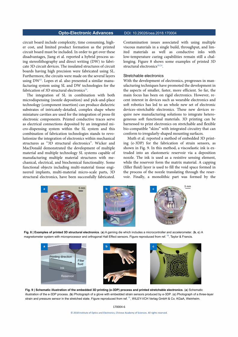
Muth et al. reported a method of embedded 3D print-ing (e-3DP) for the fabrication of strain sensors, as shown in Fig. 9. In this method, a viscoelastic ink is ex-truded into an elastomeric reservoir via a deposition nozzle. The ink is used as a resistive sensing element, while the reservoir form the matrix material. A capping (filler fluid) layer is used to fill the void space formed in the process of the nozzle translating through the reser-voir. Finally, a monolithic part was formed by the
Fig. 8 | Examples of printed 3D structural electronics. (a) A gaming die which includes a microcontroller and accelerometer. (b, c) A
magnetometer system with microprocessor and orthogonal Hall Effect sensors. Figure reproduced from ref. 18, Taylor & Francis.
5 mm a 5 mm 5 mm
b c
Fig. 9 | Schematic illustration of the embedded 3D printing (e-3DP) process and printed stretchable electronics. (a) Schematic
illustration of the e-3DP process. (b) Photograph of a glove with embedded strain sensors produced by e-3DP. (c) Photograph of a three-layer
strain and pressure sensor in the stretched state. Figure reproduced from ref. 11, WILEY-VCH Verlag GmbH & Co. KGaA, Weinheim.
Printing direction
a b c
Ink
Reservoir
Filler fluid
Opto-Electronic Advances DOI: 10.29026/oea.2018.170004
170004-7
© 2018 Institute of Optics and Electronics, Chinese Academy of Sciences. All rights reserved.
co-cure of both the reservoir and filler fluid, which cov-ered and keep the embedded conductive ink fluid. The e-3DP can create soft sensors in a highly programmable and seamless manner. In order to enable e-3DP, a multi-component materials system composed of an ink, reser-voir, and filler fluid was developed. The above method that for building highly stretchable sensors by e-3DP opens new approaches for manufacturing soft functional devices for wearable electronics, human/machine inter-faces, soft robotics, and so on11.
The ability of printing integrated circuits on the flexi-ble substrate enables the electronic devices with con-formity, lightweight structure and shock-resistant con-struction, which are challenging to be achieved by using rigid substrates such as semiconductor wafers and glass plates. Bijadi et al. have successfully tested the feasibility of a syringe extrusion-based 3D printing process to print stretchable embedded electronics through the use of SS-26S conductive silicone on flexible non-conductive silicone substrates. Instead of merely using the conduc-tive silicone traces as flexible interconnects, this method used the conductive material for creating complete cir-
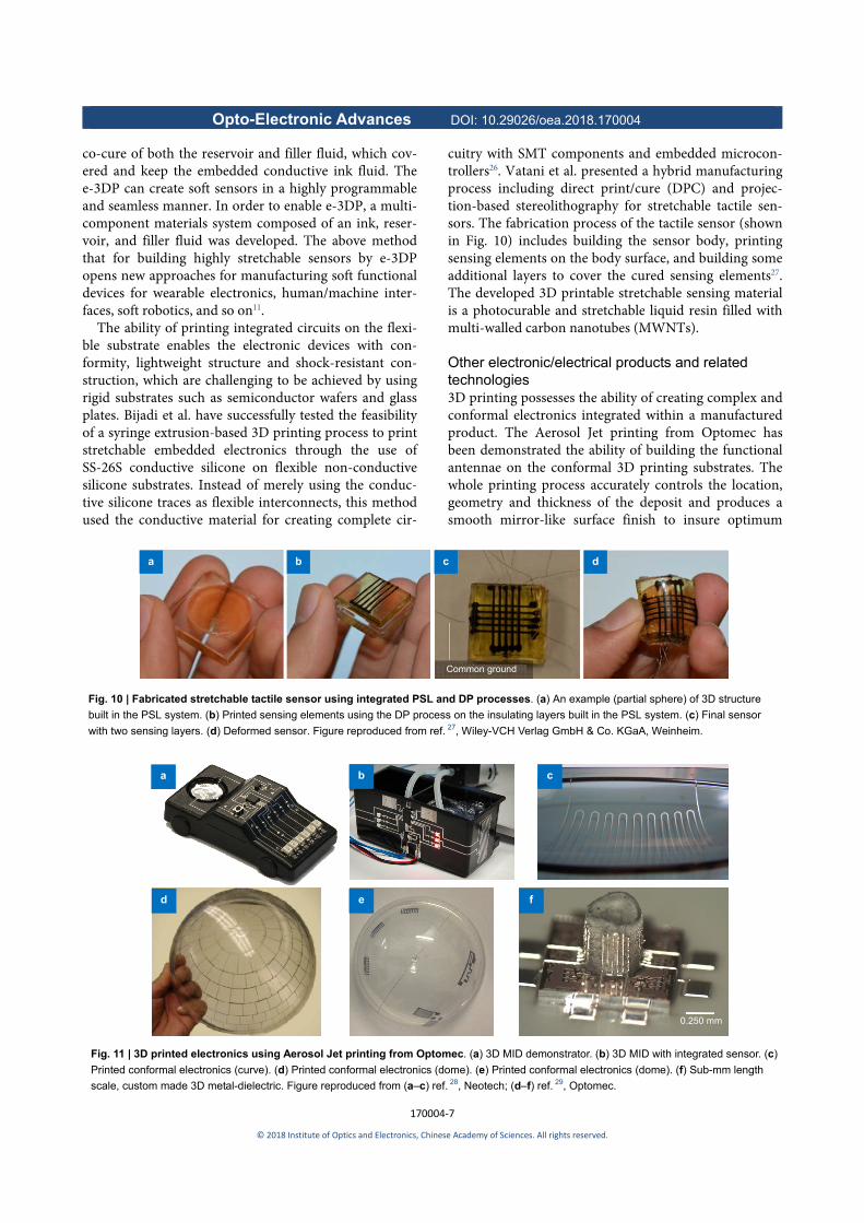
cuitry with SMT components and embedded microcon-trollers26. Vatani et al. presented a hybrid manufacturing process including direct print/cure (DPC) and projec-tion-based stereolithography for stretchable tactile sen-sors. The fabrication process of the tactile sensor (shown in Fig. 10) includes building the sensor body, printing sensing elements on the body surface, and building some additional layers to cover the cured sensing elements27. The developed 3D printable stretchable sensing material is a photocurable and stretchable liquid resin filled with multi-walled carbon nanotubes (MWNTs).
Other electronic/electrical products and related technologies 3D printing possesses the ability of creating complex and conformal electronics integrated within a manufactured product. The Aerosol Jet printing from Optomec has been demonstrated the ability of building the functional antennae on the conformal 3D printing substrates. The whole printing process accurately controls the location, geometry and thickness of the deposit and produces a smooth mirror-like surface finish to insure optimum
Fig. 10 | Fabricated stretchable tactile sensor using integrated PSL and DP processes. (a) An example (partial sphere) of 3D structure
built in the PSL system. (b) Printed sensing elements using the DP process on the insulating layers built in the PSL system. (c) Final sensor
with two sensing layers. (d) Deformed sensor. Figure reproduced from ref. 27, Wiley-VCH Verlag GmbH & Co. KGaA, Weinheim.
a b c d
Common ground
Fig. 11 | 3D printed electronics using Aerosol Jet printing from Optomec. (a) 3D MID demonstrator. (b) 3D MID with integrated sensor. (c)
Printed conformal electronics (curve). (d) Printed conformal electronics (dome). (e) Printed conformal electronics (dome). (f) Sub-mm length
scale, custom made 3D metal-dielectric. Figure reproduced from (a–c) ref. 28, Neotech; (d–f) ref. 29, Optomec.
d e
a b c
f
0.250 mm

Opto-Electronic Advances DOI: 10.29026/oea.2018.170004
170004-8
© 2018 Institute of Optics and Electronics, Chinese Academy of Sciences. All rights reserved.
antenna performance. Some kinds of mobile device an-tennas, such as the LTE, NFC, GPS, Wifi, WLAN, and BT, have been printed through the Aerosol Jet process. And the performance of such antennas tested by a cell phone component supplier is in the same level with other production methods. For now, the Aerosol Jet technolo-gy has been using for the mass production of printed 3D conformal electronics in the application of antenna and sensor. As can been seen that a hybridized DW/AM pro-cess presents great potential for creating antennas with 3-dimensional structure. Figure 11 demonstrated 3D printed electronics using Aerosol Jet printing process28–29.
Aerosol Jet printing process has the ability to print conformal interconnects on 3D surfaces eliminating the need for wire bonding – for example printing electrical connections on 3D stacked die or for LED chip fabrica-tion. Runge showed Leg prosthesis part produced from PLA (Polylactic Acid) via FDM showing complex
non-planar surfaces, with surface-integrated strain gauge sensors produced by Aerosol Jet TM printing and con-ductive paths deposited via micro-dispensing, both using the modular manufacturing platform. The structural elements of this leg prosthesis shaft were produced via the FDM process from PLA, a thermoplastic polymer. Its functionalization relies on a surface-integrated strain gauge realized via Aerosol Jet printing. The conductive paths that lead across the part as well as the contact pads at their end were deposited through micro-dispensing. The material of the resistive sensor is a silver based ink, while interconnects and contact pads are made from sil-ver particle-filled epoxy, as shown in Fig. 12 31.
The first multi-material 3D electronics printer in the world, named as Voxel8, provides an all-in-one, desktop solution for designing and prototyping next generation 3D electronic devices. Therefore, it has been regarded as a disruptive manufacture platform with the capabilities of printing embedded electronics. It enables prototyping of 3D electronic devices by the method of co-printing both thermoplastics and a highly conductive silver ink, which can be printed and cured at ambient temperature without the need for thermal annealing. Figure 13 demonstrates Voxel8 and some printed products32.
Prospect, challenges and future trends 3D printing is disrupting the design and manufacture of electronic products. Functionalities of the devic-es/products fabricated by 3D printing can be significantly expanded by incorporating electronic components, such as sensors and circuits, in predetermined cavities within fabricated structures. 3D printed objects include not only traditional mechanical characteristics, but also embedded optical and electrical functions, such as sensor; all com-plex structures are difficult to produce with existing
Fig. 13 | Voxel8 and some printed products. (a, b) Photograph of Voxel8 3D printer. (c) Printed unmanned aerial vehicle. (d) Printed antenna
(dome). (e) Printed wearable device. Figure reproduced from ref. 32, Voxel8.
ba
c d e
Fig. 12 | Leg prosthesis part produced by FDM and Aerosol Jet
printing. Figure reproduced from ref. 31, University of Applied
Science Bremerhaven.
Opto-Electronic Advances DOI: 10.29026/oea.2018.170004
170004-9
© 2018 Institute of Optics and Electronics, Chinese Academy of Sciences. All rights reserved.
manufacturing methods. Many emerging and innovative products, such as embedded electronics, 3D structural electronics, conformal electronics, stretchable electronics, etc., have been fabricated using the technologies. 3D printing electronics has been considered as the next fron-tier in AM. Optomec has developed a high volume printing solution for the production of 3D antenna and 3D sensors that are tightly integrated with an underlying product ranging from smartphones to industrial com-ponents. It can be utilized for high volume printing of conformal sensors and antennas directly onto preformed 3D structures. Complex electronics can be 3D printed at micron resolution which will enable cheaper smartphones and medical gadgets. Aerosol Jet 3D mi-cro-structure printing is capable of ultra-high resolutions with lateral features sizes of 10 μm and aspect ratios of more than 100:1 33–37.
The conductivity is still one of the major difficulties in both 3D printed electronics and general 2D printed elec-tronics because of the poor conductivity of ink caused by the low curing temperature due to the limitation of sub-strate material such as cardboard, polymers. More and more challenges in the fields of material types and pro-cessing challenges in the process of printing from 2D electronics to 3D integrated objects. Therefore, the com-patible material sets should be explored and created to provide the adequate functionality and manufacturability for the product invention by designers. Besides, the ad-hesion between the materials is also a big issue, because the conductive materials would be stripped from the substrate with a poor adhesion. This is especially im-portant case for traces that are embedded within a print and not on the surface because repair is impossible after a circuit is embedded.
In order to make electronics with 3D printing, new processes should be developed to possess the ability of depositing broader types of materials. To date, there are several solutions which have the ability to fabricate mul-tifunctional 3D structures or products with embedded functional systems. Compared to other methods, the hybrid process combining FDM and direct print/writing shows higher applied potential, more flexibility. Material jetting systems seem currently to be the most successful multi-material 3D printing process among AM technol-ogies. To date, fabrication of true 3D multiple material polymeric components using material jetting processes has been demonstrated. Currently, material jetting of polymers appears to be the nearest approximation to this vision that is currently available: The combination of high resolution, controlled material deposition with the possibility of photo polymerization, which allows imme-diate solidification of the material after printing and thus facilitates deposition of materials with different func-tional or structural roles directly besides each other, pro-
vides the foundation for effectively printing a structural electronics system directly. Multi-material and mul-ti-scale 3D printing will be the most promising solutions.
More and more 3D printed functional electronics and products with electronics will be fabricated. 3D printing electronic technology provides a powerful tool for inno-vative product development, and extends 3D printing multiple functionalities. Significant advances in 3D printing electronics have been accomplished in the re-cent years. However, there is still a long way to go for 3D printed functional electronics and products as well as their industrial-level applications. Further potentials of 3D printing electronics need still to be explored and in-vestigated.
References 1. Gibson I, Rosen D W, Stucker B. Additive manufacturing tech-
nologies (Springer, New York, 2010).
2. Derby B. Printing and prototyping of tissues and scaffolds. Sci-
ence 338, 921–926 (2012).
3. Lewis J A, Ahn B Y. Device fabrication: Three-dimensional
printed electronics. Nature 518, 42–43 (2015).
4. Kong Y L, Tamargo I A, Kim H, Johnson B N, Gupta M K et al.
3D printed quantum dot light-emitting diodes. Nano Lett 14,
7017–7023 (2014).
5. Lan H. Active mixing nozzle for multimaterial and multiscale
three-dimensional printing. J Micro Nano-Manuf 5, 040904
(2017).
6. Zheng X, Smith W, Jackson J, Moran B, Cui H et al. Multiscale
metallic metamaterials. Nature Mater 15, 1100–1106 (2016).
7. Vaezi M, Seitz H, Yang S. A review on 3D micro-additive manu-
facturing technologies. Int J Adv Manuf Technol 67, 1721–1754
(2013).
8. Tian X Y, Yin L X, Li D C. Current situation and trend of fabrica-
tion technologies for three-dimensional metamaterials. Opto-
Electron Eng 44, 69–76 (2017).
9. Espalin D, Muse D W, MacDonald E, Wicker R B. 3D Printing
multifunctionality: structures with electronics. Int J Adv Manuf
Technol 72, 963–978 (2014).
10. Lu Y, Vatani M, Choi J W. Direct-write/cure conductive polymer
nanocomposites for 3D structural electronics. J Mech Sci
Technol 27, 2929–2934 (2013).
11. Muth J T, Vogt D M, Truby R L, Mengüç Y, Kolesky D B et al.
Embedded 3D printing of strain sensors within highly stretcha-
ble elastomers. Adv Mater 26, 6307–6312 (2014).
12. Wu S Y, Yang C, Hsu W, Lin L. 3D-printed microelectronics for
integrated circuitry and passive wireless sensors. Microsys
Nanoeng 1: 15013 (2015).
13. Sun K, Wei T S, Ahn B Y, Seo J Y, Dillon S J et al. 3D Printing of
interdigitated Li-Ion microbattery architectures. Adv Mater 25,
4539–4543 (2013).
14. Lehmhus D, Aumund-Kopp C, Petzoldt F, Godlinskic D,
Haberkorn A et al. Customized smartness: a survey on links
between additive manufacturing and sensor integration.
Procedia Tech 26: 284–301 (2016).
15. Ladd C, So J H, Muth J, Dickey M D. 3D printing of free stand-
ing liquid metal microstructures. Adv Mater 25, 5081–5085

Opto-Electronic Advances DOI: 10.29026/oea.2018.170004
170004-10
© 2018 Institute of Optics and Electronics, Chinese Academy of Sciences. All rights reserved.
(2013).
16. Lifton V A, Lifton G, Simon S. Options for additive rapid proto-
typing methods (3D printing) in MEMS technology. Rapid Proto-
typing J 20, 403–412 (2014).
17. MacDonald E, Wicker R. Multiprocess 3D printing for increasing
component functionality. Science 353: aaf2093 (2016).
18. Wicker R B, MacDonald E W. Multi-material, multi-technology
stereolithography. Virtual Phys Prototyping 7, 181–194 (2012).
19. Kief C J, Aarestad J, Macdonald E, Shemelya C, Roberson D A
et al. Printing multi-functionality: additive manufacturing for
CubeSats. In AIAA SPACE 2014 Conference and Exposition,
AIAA SPACE Forum 4193 (AIAA, 2014);
https://doi.org/10.2514/6.2014-4193
20. Liang M, Shemelya C, MacDonald E, Wicker R, Xin H. 3D
printed microwave patch antenna via fused deposition method
and ultrasonic wire mesh embedding technique. IEEE Antennas
Wireless Propag Lett 14, 1346–1349 (2015).
21. Shemelya C, Cedillos F, Aguilera E, Espalin D, Muse D et al.
Encapsulated copper wire and copper mesh capacitive sensing
for 3-D printing applications. IEEE Sens J 15, 1280–1286
(2015).
22. Ready S, Whiting G, Ng T N. Multi-material 3D printing. In NIP &
Digital Fabrication Conference, 2014 International Conference
on Digital Printing Technologies 120–123 (2014).
23. Pa P, Larimore Z, Parsons P, Mirotznik M. Multi-material addi-
tive manufacturing of embedded low-profile antennas. Electron
Lett 51, 1561–1562 (2015).
24. Lopes A J, MacDonald E, Wicker R B. Integrating
stereolithography and direct print technologies for 3D structural
electronics fabrication. Rapid Prototyping J 18, 129–143 (2012).
25. Jang S H, Oh S T, Lee I H, Kim H C, Cho H Y. 3-Dimensional
circuit device fabrication process using stereolithography and
direct writing. Int J Precis Eng Man 16, 1361–1367(2015).
26. Bijadi S. Feasibility of additive manufacturing method for devel-
oping stretchable and flexible embedded circuits (University of
Minnesota, Minneapolis, USA, 2014).
27. Vatani M, Lu Y, Engeberg E D, Choi J W. Combined 3D printing
technologies and material for fabrication of tactile sensors. Int J
Precis Eng Man 16, 1375–1383 (2015).
28. Hedges M. 3D Printed Electronics via Aerosol Jet (Neotech,
2014).
29. Optomec. https://www.optomec.com (2017).
30. Cai F, Pavlidis S, Papapolymerou J, Chang Y H, Wang K et al.
Aerosol jet printing for 3-D multilayer passive microwave circuit-
ry. In IEEE European Microwave Conference (IEEE, 2014);
http://doi.org/10.1109/EuMC.2014.6986483
31. Runge D. 3D-Printing und gedruckte Elektronik für die
Medizintechnik (University of Applied Science Bremerhaven,
Bremen Area, Germany, 2016).
32. Voxel8. https://www.voxel8.com (2017).
33. Dickey M. Liquid metals for soft and stretchable electronics. In
Stretchable Bioelectronics for Medical Devices and Systems.
Microsystems and Nanosystems (Springer, Cham, 2016);
https://doi.org/10.1007/978-3-319-28694-5_1
34. Rahman M T, Rahimi A, Gupta S, Panata R. Microscale additive
manufacturing and modeling of interdigitated capacitive touch
sensors. Sensor Actuat A-Phys 248, 94–103 (2016).
35. Donnell J, Kim M, Yoon H. A review on electromechanical de-
vices fabricated by additive manufacturing. ASME J Manuf Sci
E-T 139, 010801 (2017).
36. Thompson B, Yoon H S. Aerosol-printed strain sensor using
PEDOT: PSS. IEEE Sens J 13, 4256–4263 (2013).
37. Madden K E, Deshpande A D. On integration of additive manu-
facturing during the design and development of a rehabilitation
robot: a case study. ASME J Mech Des 137, 111417 (2015).
Acknowledgements We are grateful for financial supports from the National Natural Science Foundation of China (51775288).
Competing interests The authors declare no competing financial interests.