Adaptive RF front-ends : providing resilience to changing ... · providing resilience to changing...
212
Adaptive RF front-ends : providing resilience to changing environments van Bezooijen, A. DOI: 10.6100/IR658779 Published: 01/01/2010 Document Version Publisher’s PDF, also known as Version of Record (includes final page, issue and volume numbers) Please check the document version of this publication: • A submitted manuscript is the author's version of the article upon submission and before peer-review. There can be important differences between the submitted version and the official published version of record. People interested in the research are advised to contact the author for the final version of the publication, or visit the DOI to the publisher's website. • The final author version and the galley proof are versions of the publication after peer review. • The final published version features the final layout of the paper including the volume, issue and page numbers. Link to publication Citation for published version (APA): Bezooijen, van, A. (2010). Adaptive RF front-ends : providing resilience to changing environments Eindhoven: Technische Universiteit Eindhoven DOI: 10.6100/IR658779 General rights Copyright and moral rights for the publications made accessible in the public portal are retained by the authors and/or other copyright owners and it is a condition of accessing publications that users recognise and abide by the legal requirements associated with these rights. • Users may download and print one copy of any publication from the public portal for the purpose of private study or research. • You may not further distribute the material or use it for any profit-making activity or commercial gain • You may freely distribute the URL identifying the publication in the public portal ? Take down policy If you believe that this document breaches copyright please contact us providing details, and we will remove access to the work immediately and investigate your claim. Download date: 31. May. 2018
Transcript of Adaptive RF front-ends : providing resilience to changing ... · providing resilience to changing...

Adaptive RF front-ends : providing resilience to changingenvironmentsvan Bezooijen, A.
DOI:10.6100/IR658779
Published: 01/01/2010
Document VersionPublisher’s PDF, also known as Version of Record (includes final page, issue and volume numbers)
Please check the document version of this publication:
• A submitted manuscript is the author's version of the article upon submission and before peer-review. There can be important differencesbetween the submitted version and the official published version of record. People interested in the research are advised to contact theauthor for the final version of the publication, or visit the DOI to the publisher's website.• The final author version and the galley proof are versions of the publication after peer review.• The final published version features the final layout of the paper including the volume, issue and page numbers.
Link to publication
Citation for published version (APA):Bezooijen, van, A. (2010). Adaptive RF front-ends : providing resilience to changing environments Eindhoven:Technische Universiteit Eindhoven DOI: 10.6100/IR658779
General rightsCopyright and moral rights for the publications made accessible in the public portal are retained by the authors and/or other copyright ownersand it is a condition of accessing publications that users recognise and abide by the legal requirements associated with these rights.
• Users may download and print one copy of any publication from the public portal for the purpose of private study or research. • You may not further distribute the material or use it for any profit-making activity or commercial gain • You may freely distribute the URL identifying the publication in the public portal ?
Take down policyIf you believe that this document breaches copyright please contact us providing details, and we will remove access to the work immediatelyand investigate your claim.
Download date: 31. May. 2018

Adaptive RF front-ends, providing resilience to changing environments
André van Bezooijen

Printed by Printservice TU/e Cover design: Paul Verspaget & Carin Bruinink; Grafische Vormgeving - Communicatie

Adaptive RF front-ends, providing resilience to changing environments
Proefschrift
ter verkrijging van de graad van doctor aan de Technische Universiteit Eindhoven, op gezag van de rector magnificus, prof.dr.ir. C.J. van Duijn, voor een
commissie aangewezen door het College voor Promoties in het openbaar te verdedigen op donderdag 8 april 2010 om 16.00 uur
door
Adrianus van Bezooijen
geboren te Klundert

Dit proefschrift is goedgekeurd door de promotor: prof.dr.ir. A.H.M. van Roermund Copromotor: dr.ir. R. Mahmoudi A catalogue record is available from the Eindhoven University of Technology Library ISBN: 978-90-386-2184-5 Copyright © 2010 by André van Bezooijen All rights reserved. No part of this publication may be reproduced, stored in a retrieval system, or transmitted in any form or by any means without the prior written permission of the copyright owner.

Aan José

Samenstelling promotiecommissie: prof.dr.ir. A.C.P.M. Backx Voorzitter dr.ir. A.P. de Hek TNO Den Haag
dr.ir. R. Mahmoudi Universiteit Eindhoven prof.dr.ir. A.H.M. van Roermund Universiteit Eindhoven
prof.dr.ir. A.B. Smolders Universiteit Eindhoven prof.dr.ir. F.E. van Vliet Universiteit Twente dr.ing. L.C.N. de Vreede Universiteit Delft dr.ir. S. Weiland Universiteit Eindhoven

vii
Symbols A Capacitor plate area
Ai Current wave amplitude
AIN Input signal amplitude
Au Voltage wave amplitude
Ax Amplitude of detector input signal x
Ay Amplitude of detector input signal y
B Susceptance
BC_PAR Susceptance of parallel capacitor
BDET Detected susceptance
BINT Susceptance at an intermediate network node
BL_PAR Susceptance of parallel inductor
BM Matching susceptance
BVCBO Collector-base breakdown voltage for open emitter
BVCEO Collector-emitter breakdown voltage for open base
C Capacitor
CARRAY Switched capacitor array capacitance
CDC DC-block capacitor
CIN Input capacitor of differentially controlled PI-network
CHOLD T&H circuit Hold Capacitor
CMEMS MEMS capacitance
CMID Middle capacitor of dual-section PI-network
COFF OFF capacitance
CON ON capacitance
COUT Output capacitor of differentially controlled PI-network
CP Parasitic capacitor
CPAR Parallel capacitance
CSERIES Series capacitance
CUNIT Unit cell capacitance

viii
CR Capacitance tuning ratio
CRARRAY Array capacitance tuning ratio
CRC_SERIES Tuning ratio of series capacitor
CRMEMS MEMS ON/OFF capacitance ratio
D Disturbing signal
e error
ER Relative error
FE Electro-static force
FM Mechanical force
fT Transistor cut-off frequency
g Gap height
g0 Gap height at zero bias
G Conductance
G Gain
GC_PAR Conductance of parallel capacitor
GDET Detected conductance
GLOAD Load conductance
GL_PAR Conductance of parallel inductor
GM Matching conductance
GREF Reference conductance
GT Threshold amplifier gain of OTP loop
GU Threshold amplifier gain of OVP loop
H, H1, H2 Transfer gain
HE Error amplifier gain
HER Error amplifier gain of real loop
HEX Error amplifier gain of imaginary loop
HR Matching network transfer gain of real part
HT PA temperature transfer function
HU PA voltage transfer function
HX Matching network transfer gain of imaginary part

ix
i Branch current
IAV Avalanche current
IB Base current
ICOL Collector current
IC_CRIT Critical collector current
IEM Emitter current
IPROT Protection circuit output current
ITHR Threshold current
I(t) In-phase signal
IL Insertion Loss
I0 Saturation current
k RF-MEMS spring constant
k Boltzmann’s constant 1.38e-23 J/K
KD Detector constant
KDR Detector constant of the resistance detector
KDX Detector constant of the reactance detector
LE Emitter inductance
LPAR Parallel inductance
LSERIES Series inductance
Mn Avalanche multiplication factor
PDET Detected output power
PDISS Dissipated power
PIN Input power
PINC Incident power
PLOAD Load power
POUT Output power
PTRX Power delivered by transceiver
PREF Reference power
PSUP Supply power
q Electric charge of a single electron 1.60e-19 C

x
Q(t) Quadrature signal
r Ratio between DC-block and RF-MEMS capacitance
R Resistance
RBIAS Resistance of RF-MEMS biasing resistor
RCROSS Bond frame crossing resistance
RC_SERIES Resistance of series capacitor
RDC DC-blocking capacitor series resistance
RDET Detected resistance
RB Base resistance
RE Emitter resistance
REQ Equivalent resistance
RLOAD Load resistance
RLR Return loss reduction
RL_SERIES Resistance of series inductor
RM Matching resistance
RMEMS MEMS series resistance
RNOM Nominal resistance
RREF Reference resistance
RS Source resistance
RSUB Substrate resistance
RSUB Substrate resistance
RTH Thermal resistance
RTHR Threshold resistor
SoLG Sum of loop gains
td Dielectric thickness
tr Equivalent roughness thickness
TAMB Ambient temperature
TDET Detected temperature
TDIE Die temperature
Tj Junction temperature

xi
u nodal voltage
UACT RF-MEMS actuation voltage
UBAT Battery voltage
UBIAS Bias voltage
UBE Base-emitter voltage
UCB Collector-base voltage
UCE Collector-emitter voltage
UCOL Collector voltage
UDAC Control voltage from Digital-to-Analogue Converter
U*DAC Adapted UDAC
UEQ Equivalent voltage
UPI RF-MEMS pull-in voltage
UPO RF-MEMS pull-out voltage
UQ Bias voltage
UREF Reference voltage
USUP Supply voltage
UT Thermal voltage
v+COL Incident voltage wave
v-COL Reflected voltage wave
vCOL(t) Collector voltage
VACT Actuation voltage
VCONTROL Control voltage
VDETECTOR Detected voltage
VHOLD Hold voltage
VPI Pull-in voltage
VPO Pull-out voltage
VREF Reference voltage
VSUPPLY Supply voltage
X Reactance
X Input signal

xii
XC_SERIES Reactance of series capacitor
XDET Detected reactance
XINT Reactance at an intermediate network node
XL_SERIES Reactance of series inductor
XM Matching reactance
XREF Reference reactance
XSENSE Sense reactance
Y Admittance
Y Output signal
YINT Intermediate admittance
YLOAD Load admittance
YM Matching admittance
YREF Reference admittance
YSHUNT Shunt admittance
Z Impedance
ZANT Antenna impedance
Z0 Characteristic impedance
ZINT Intermediate impedance
ZM Matching impedance
ZLOAD Load impedance
∆BC Variable capacitor susceptance
∆XL Variable inductor reactance
β0 Transistor current gain
εr Relative dielectric constant
ε0 Dielectric constant 8.885 e-12 F/m
Γ Reflection coefficient
ΓCOL Collector reflection coefficient
ΓLOAD Load reflection coefficient
ΓΜ Matching reflection coefficient

xiii
η Efficiency
φ Base-emitter temperature dependency (~ -1mV/˚C)
φDET Detected phase of impedance Z
φi Current wave phase
φu Voltage wave phase
φx Phase of detector input signal x
φy Phase of detector input signal y
φZ Phase of impedance Z
θ Phase of reflection coefficient
ω angular frequency


xv
Abbreviations ACPR Adjacent Channel Power Rejection
ADS Advanced Design System
AWS Advanced Wireless Service
BiCMOS Bipolar-CMOS
BST Barium-Strontium-Titanate
BAW Bulk Acoustic Wave
CdmaOne Code Division Multiple Access One
CL Closed Loop
CMOS Complementary MOS
CV-curve Capacitance vs. Voltage characteristic
DC Direct Current
DS Detector Sensitivity
EDGE Enhanced Data rates for GSM Evolution
EN Base-band controller ENable signal
ESD Electro Static Discharge
ESL Equivalent Series inductance (L)
EVM Error Vector Magnitude
FDD Frequency Division Duplex
FEM Front End Module
GPS Global Positioning System
GSM Global System for Mobile communication
GaAs Gallium Arsenide
HB High Band
HBT Hetero-junction Bipolar Transistor
HSPA High Speed Packet Access
HV-NPN High Voltage NPN-transistor
IC Integrated Circuit
IM3 Third-order Inter Modulation distortion

xvi
LB Low band
LNA Low Noise Amplifier
LSB Least Significant Bit
LTCC Low Temperature Co-fired Ceramic
LTE Long Term Evolution
LUT Look-Up Table
MEMS Micro Electro Mechanical System
MIM Metal-Insulator-Metal
MOS Metal-Oxide-Silicon
MSB Most Significant Bit
OL Open Loop
OCP Over Current Protection
OM Output Match
OTP Over Temperature Protection
OVT Over Voltage Protection
PA Power Amplifier
PAM Power Amplifier Module
PASSI PASsive Silicon
PCB Printed Circuit Board
PCL Power Control Loop
pHEMT Pseudo-morphic High Electron Mobility Transistor
PIFA Planar Inverted-F Antenna
PIN P-type Intrinsic N-type doped regions
Q Quality (-factor)
RF Radio Frequency
RMS Root-Mean-Square
Rx Receiver
SAW Surface Acoustic Wave
Si Silicon
SMD Surface Mounted Device

xvii
SoS Silicon On Sapphire
SOI Silicon On Insulator
TDMA Time Division Multiple Access
TRx Transceiver
Tx Transmitter
T&H Track-and-Hold
UMTS Universal Mobile Communications System
VGA Variable Gain Amplifier
VSWR Voltage Standing Wave Ratio
W-CDMA Wide-band Code Division Multiple Access
WLAN Wireless Local Area Network
WiMAX Worldwide Interoperability for Microwave Access


xix
Contents
Symbols..........................................................................................................vii
Abbreviations ................................................................................................ xv
Contents........................................................................................................ xix
1 Introduction........................................................................................... 1
1.1 Context and trends in wireless communication .................................. 1 1.2 Resilience to unpredictably changing environments........................... 2 1.3 Improvements by adaptively controlled RF front-ends ...................... 5 1.4 Aim and scope of the thesis ................................................................ 6 1.5 Thesis outline ...................................................................................... 7
2 Adaptive RF frond-ends........................................................................ 11
2.1 Introduction ....................................................................................... 11 2.2 RF front-end functionality................................................................. 12
2.2.1 Antenna switch ........................................................................... 12 2.2.2 Power amplifier .......................................................................... 13 2.2.3 Duplexer ..................................................................................... 15 2.2.4 Blocking filter............................................................................. 16
2.3 Fluctuations in operating conditions ................................................. 17 2.4 Impact of variables ............................................................................ 20
2.4.1 Current fluctuation...................................................................... 20 2.4.2 Voltage fluctuation ..................................................................... 22 2.4.3 Die temperature fluctuation........................................................ 25 2.4.4 Efficiency fluctuation ................................................................. 26 2.4.5 Discussion on the impact of variables ........................................ 28
2.5 Adaptive control theory..................................................................... 29 2.6 Identification of variables for detection and correction .................... 31
2.6.1 Independent variables ................................................................. 32 2.6.2 Dependent variables ................................................................... 33
2.7 Conclusions on adaptive RF front-ends ............................................ 37
3 Adaptive impedance control .............................................................. 39
3.1 Introduction ....................................................................................... 39 3.1.1 Dimensionality ........................................................................... 41 3.1.2 Non-linearity............................................................................... 43 3.1.3 Robust control ............................................................................ 46

xx
3.1.4 Impedance tuning region ............................................................ 50 3.1.5 Insertion loss............................................................................... 51 3.1.6 System gain ................................................................................ 52
3.2 Mismatch detection method .............................................................. 54 3.2.1 Sensing ....................................................................................... 54 3.2.2 Detector concept ......................................................................... 55 3.2.3 Simulation results ....................................................................... 57 3.2.4 Conclusions on mismatch detection ........................................... 58
3.3 Adaptively controlled PI-networks using differentially controlled capacitors..................................................................................................... 59
3.3.1 Concept....................................................................................... 60 3.3.2 Differentially controlled single-section PI-network ................... 61 3.3.3 Differentially controlled dual-section PI-network...................... 65 3.3.4 Simulations ................................................................................. 66 3.3.5 Conclusions on adaptively controlled PI-networks .................... 71
3.4 Adaptively controlled L-network using cascaded loops ................... 73 3.4.1 Concept....................................................................................... 73 3.4.2 Actuation .................................................................................... 74 3.4.3 Convergence ............................................................................... 77 3.4.4 Simulations ................................................................................. 80 3.4.5 Capacitance tuning range requirement ....................................... 83 3.4.6 Insertion loss............................................................................... 86 3.4.7 Tuning range requirement .......................................................... 86 3.4.8 Conclusions on adaptively controlled L-network....................... 88
3.5 Adaptive series-LC matching network using RF-MEMS................. 91 3.5.1 Adaptive tuning system .............................................................. 91 3.5.2 Adaptive RF-MEMS system design........................................... 97 3.5.3 Experimental verification ......................................................... 105 3.5.4 Conclusions on adaptive series-LC matching module ............. 109
3.6 Load line adaptation........................................................................ 110 3.6.1 Introduction .............................................................................. 110 3.6.2 Concept..................................................................................... 111 3.6.3 Implementation of load line adaptation .................................... 113 3.6.4 Simulation results ..................................................................... 114 3.6.5 Conclusions on load line adaptation......................................... 116
3.7 Conclusions on adaptive impedance control................................... 117
4 Adaptive power control .................................................................... 119
4.1 Introduction ..................................................................................... 119 4.1.1 Over-voltage protection for improved ruggedness................... 119 4.1.2 Over-temperature protection for improved ruggedness............ 120

xxi
4.1.3 Under-voltage protection for improved linearity...................... 121 4.2 Safe operating conditions ................................................................ 122 4.3 Power adaptation for ruggedness .................................................... 126
4.3.1 Concept..................................................................................... 126 4.3.2 Simulations ............................................................................... 127 4.3.3 Over-voltage protection circuit................................................. 129 4.3.4 Over-temperature protection circuit ......................................... 130 4.3.5 Technology ............................................................................... 131 4.3.6 Experimental verification ......................................................... 131
4.4 Power adaptation for linearity ......................................................... 136 4.4.1 Concept..................................................................................... 136 4.4.2 Simulations ............................................................................... 136 4.4.3 Circuit design............................................................................ 139 4.4.4 Experimental verification ......................................................... 140
4.5 Conclusions on adaptive power control .......................................... 143
5 Conclusions ........................................................................................ 145
Recommendations....................................................................................... 147
Original contributions................................................................................ 149
Publications ................................................................................................. 151
Patents . ....................................................................................................... 155
Appendix A Overview of adaptively controlled matching networks.... 157
Appendix B A dual-banding technique ................................................... 163
Appendix C Transistor breakdown voltages .......................................... 165
References ................................................................................................... 173
Acknowledgement....................................................................................... 181
Summary ..................................................................................................... 183
Samenvatting............................................................................................... 185
Biography .................................................................................................... 187

xxii
Biografie ...................................................................................................... 189

1
Chapter
1 Introduction
1.1 Context and trends in wireless communication During the last century, technological innovations have been changing our ways
of communication tremendously. The inventors and pioneering engineers of both the telephone [1] and radio [2], [3] were fascinated by the idea of exchanging real-time information over large distances, and their audience of first successful demonstrations were astonished and excited.
The big success of wired telephony and radio inspired the development of wireless mobile communication devices, like pack-sets, as forerunners of walkie-talkies and pagers [4], [5]. The first mobile radios, still using valves in those days, needed very heavy battery packs and were far from user-friendly.
Thanks to the invention of the transistor [6] and integrated circuit technology [7] their successors could be made much smaller and lighter. CMOS technology, digital circuit techniques and software paved the way for user-friendly handsets, partly due to the introduction of automatic tuning of the radio, and they enabled many features at low cost.
Nowadays, mobile communication is part of our social life [8]. Cellular networks connect people, any time anywhere, and they allow for the exchange of an ever-increasing amount of (real-time) information.
To a great extent, the information society of the 21st century will be mutually dependent on mobile communication networks, posing severe requirements on the quality of services. Therefore, the availability of high capacity reliable links as well as that of robust and user-friendly handsets will become even more important.
The ever increasing demand for channel capacity of mobile communication
networks result in a steadily increasing number of frequency bands that are deployed in various parts of the world. Regularly, new communication standards are defined that use spectrum efficient modulation schemes and provide channel capacity that is adaptable to the users needs, of which the Advanced Wireless Service (AWS), High Speed Packet Access (HSPA), and Long Term Evolution (LTE) are recent examples [9].

2
Besides the RF-link that provides connection to the cellular infrastructure, many handsets can set-up an additional RF-link for short range data communication, using Bluetooth, WLAN (Wireless Local Area Network) or WiMAX (Worldwide Interoperability for Microwave Access), and have additional receivers for FM-radio, GPS (Global Positioning System) or even TV-on-mobile. The last few years, co-habitation of these radios in a small handset is getting more attention because the design of these multi-radio handsets turns out to be very challenging, for instance, because of mutual interference.
Since various wireless communication protocols are deployed in many different frequency bands, multi-mode multi-band phones (and components) are desired in order to benefit from economy of scale, and it allows the users to use their phone in many countries around the globe. Software defined radios facilitate such a flexible operation, in particular that of the digital and analog parts of the phone.
For the RF front-end part, multi-band phones commonly use several narrow-band
RF signal paths in parallel because a single wide-band RF signal path cannot meet the very demanding requirements on receiver sensitivity and transceiver spurious emission.
Currently, re-configurable RF systems are being investigated [10] in order to reduce, at least partly, the number of parallel RF signal paths and hence, to reduce cost and size. These re-configurable RF systems require unusually linear, low loss switches with a large ON/OFF impedance ratio. The performance of classic PIN diode switches and pHEMT switches [11] is often insufficient to meet the requirements. But, recent advances in the development of RF-MEMS devices [12], CMOS switches on sapphire [13] as well as on high resistive silicon (HRS) will most likely enable the implementation of re-configurable RF front-ends in the near future.
The RF front-end is a very important part of a cellular phone, because typically it
consumes most of the power and therefore determines the talk-time. Furthermore, since the RF front-end is optimized for efficiency it is typically the most non-linear part of the transmitter and therefore determines the quality of the RF link.
Because efficiency is so important, many efficiency enhancement techniques are under investigation, like: Envelope Tracking [16], Polar Loop [17], Doherty [18], and, since a few years, load line modulation [19]. All these techniques offer efficiency enhancement compared to a classic class-AB power amplifier, but, in addition, they often require adaptive control loops to meet the stringent linearity requirements.
1.2 Resilience to unpredictably changing environments Nowadays, many different functions are built in handsets, but their main

3
functionality remains that of a telephone combined with a radio receiver and transmitter to provide wireless connection between the handset and the cellular network infrastructure. A block diagram of this basic functionality is depicted in Figure 1.
TRxFEM Base-bandControler
Userinterface
Rx 1800 MHz
Tx 900 MHz
Tx 1800 MHzPA
Rx 900 MHz
Rx UMTSTx UMTSOM
PA
Ant
Duplexer
Ant. switch Blocking filter
OM
OM
Figure 1. A block diagram of a typical multi-mode, multi-band mobile phone and its front-end module.
The front-end module (FEM) connects the antenna to selected transmitter (Tx) and receiver (Rx) signal paths that are frequency-band selective in order to minimize spurious emission and reception.
An important trend is that RF front-end functionality and complexity increases steadily because the number of mobile phone frequency-bands and communication standards keeps on getting larger in order to accommodate the growing need for channel capacity.
Monolithic integration of all RF front-end functionality is impossible because of the many contradicting requirements that are posed on the various functions. Therefore, RF front-ends are commonly realized as a module; an assembly of components placed on a common carrier and encapsulated into one package, while each component uses a dedicated technology.
To meet all specifications RF front-ends need to be resilient to changes in the environment in which the RF front-end module operates. The variables describing this changing environment can be categorized in two groups: predictable, and

4
unpredictable variables.
Predictably changing variables: • Output power • Operating frequency • Mode dependent modulation
Unpredictably changing variables:
• Antenna impedance variations due to: o Body-effects o Change in phone form factor o Narrow antenna bandwidth
• Supply voltage variations due to: o Battery charging and de-charging
• Temperature variations of the handset due to o Ambient o Dissipation determined by:
Output power Antenna impedance Supply voltage
The variables: output power, operating frequency, and type of modulation are
called predictable because, from a handset point of view, their absolute values and moments of change, are a priori known since they are determined by the cellular infrastructure and passed over to the handset. The variables: antenna impedance, supply voltage, and temperature are called unpredictable because the handset has no a priori knowledge on their absolute value nor on their rate of change.
Since the variables, from both categories, vary over wide ranges, large design margins are typically needed to realize resilient RF front-ends, which compromises the trade-offs to be made between the main performance parameters like:
• Maximum output power • Efficiency • Linearity • Ruggedness • Receiver sensitivity
RF front-end design requirements can be relaxed by using a priori knowledge on
the predictably varying variables to re-configure the RF front-end. For example, the base-band controller commonly selects the appropriate Rx/Tx line-up, activates biasing circuitry that is optimized per mode of operation, and adjusts the output power for optimum link quality. Such re-configurability, however, can not be used

5
to correct for unpredictably changing variables due to a lack of a priori knowledge.
The problem addressed in this thesis is to improve mobile phone RF front-end performance, when operating in unpredictably changing environments.
1.3 Improvements by adaptively controlled RF front-ends In principle, the performance of a system operating in a changing environment
will improve when the system is able to adapt itself to that environment. The goal of this thesis work is to explore adaptive control techniques in order to improve one or more of the following RF front-end parameters:
• Maximum output power
Under poor propagation conditions, the cellular infrastructure requests the handset to transmit at maximum output power. The effective maximum output power will reduce, however, when, under influence of body-effects, the load impedance of the power transistor increases. Adaptive control of the load impedance will secure the maximum output power and hence, it will improve link quality and thus the cellular network coverage under real life user conditions.
• Efficiency At medium output power, the efficiency of a power amplifier depends on the load impedance of the power transistor and therefore, the efficiency varies under influence of fluctuating body-effects. Adaptive control of the load impedance will avoid low efficiencies and will maintain the talk-time of the phone under user conditions.
• Linearity At high output power the amplifier linearity is strongly affected by the antenna environment and the battery supply voltage due to collector voltage saturation. Various adaptive methods can be used to prevent the power transistor from saturating and thus to preserve the modulation quality under extremes conditions.
• Ruggedness To avoid destructive breakdown of the power transistor, while it operates under concurrent extremes in output power, antenna mismatch, and supply

6
voltage, power amplifier optimized IC processes and large design margins are needed. Adaptive output power control techniques can be used to limit the collector peak voltage, die temperature, and/or collector current, when needed, in order to protect the power transistor against over-voltage, over-temperature, and/or over-current conditions respectively. This allows the use of standard silicon bipolar technology for the implementation of the power amplifier. Alternatively, the ruggedness of a power amplifier can be secured by adaptive techniques that reduce the extremes in antenna impedance and supply voltage.
• Receiver sensitivity Detuning of the antenna resonance frequency results in reduced sensitivity of the receiver, which can partly be recovered by adaptive correction of the antenna impedance.
1.4 Aim and scope of the thesis The aim of this thesis is to investigate adaptive control techniques in order to
improve the performance of mobile phone RF front-ends that operate in unpredictably changing environments.
In this thesis two adaptive techniques are treated in particular:
• impedance control, and • power control.
These two techniques define the scope of this thesis. They have been investigated because both were identified as very promising methods, as discussed in Chapter 2. Each of these two approaches has distinct advantages and disadvantages.
The main advantage of adaptive impedance control is that compensation of
antenna impedance fluctuations eliminates the impact of the parameter that affects RF front-end performance most.
But, system specifications pose severe requirements on insertion loss, distortion and tuning range of the variable capacitors, which are very difficult to meet. Therefore, new enabling technologies are being developed, of which RF-MEMS is one of them. Since the development of new reliable technologies usually takes many years, adaptive impedance control can be seen as a solution on the long term.
Since the power control concepts, treated in this thesis, are aiming for the use of standard silicon technology for the implementation of power amplifiers and their protection circuitry, these techniques can be considered as a short-term solution in making RF frond-ends more resilient to fluctuations.
The adaptive power control techniques presented are based on limiting the output

7
power under extremes. Hence, they do not eliminate the main causes of these extremes, which forms a basic limitation of this approach.
A number of topics that are relevant in improving RF front-end performance are
kept outside the scope of this thesis. Some of these topics are briefly discussed below.
Several voltage supply adaptation techniques are well known: • supply voltage control of the power transistor for setting the phone output
power in GSM-mode [20], using a modulation with constant envelope, • supply voltage tracking in accordance to the average output power [21], [22]
in EDGE and W-CDMA-mode, using a non-constant envelope modulations, and
• envelope tracking [23] and polar modulation [24], [25] make use of supply voltage adaptation in accordance to the momentarily output power of amplitude modulated signals.
Although these techniques provide power amplifier efficiency improvement, they do not eliminate the impact of unpredictable load impedance variations. They do not preserve maximum output power and do not prevent excessive collector currents nor die temperatures under worst case load conditions.
The antenna impedance matching that is achieved, adaptively, at the frequency of
transmission, can be sub-optimal at the frequency of reception, especially when Tx and Rx frequencies are wide apart [26], [27]. Methods that provide optimum trade-offs in matching at Tx and Rx frequencies have not been investigated.
Adaptive impedance control techniques for receive-only modes (FM reception, television reception, GPS, etc.) have not been treated. For such modes, obtaining reliable information on mismatch is not easy.
Technologies for highly linear and low loss varactors and semiconductor switches
are under development. In this thesis varactor and semiconductor based variable capacitors for the implementation of tunable matching networks have not been considered.
For this thesis, the reliability of power amplifiers and RF-MEMS devices is kept out of scope.
1.5 Thesis outline Chapter 2 describes the functionality of a mobile phone RF front-end. It explains
that specifications on linearity, spurious emission, sensitivity, and power efficiency,

8
etc. pose contradicting requirements that are difficult to meet, especially because the RF front-end needs to operate in a strongly changing environment. In order to provide insight on the impact of unpredictably changing variables (like antenna load impedance, battery supply voltage, etc.) on the RF front-end performance, a mathematical analysis is presented. Then, adaptive control is introduced as a solution in making systems independent of unpredictably changing environments. The variables that are most suited for detection and actuation are identified in a systematic manner, which results in a further investigation of two promising techniques: adaptive impedance control and adaptive power control, as visualized in Figure 2.
In Chapter 3 adaptive impedance control techniques are presented that make RF
front-ends resilient to antenna impedance variations. Since robust control over a wide impedance region is challenging, first some basic properties of impedance control are introduced, like its 2-dimensionality and the non-linear impedance transformation of high-order matching networks. To satisfy 2-dimensional control a true-orthogonal detector is presented that can provide mismatch information in the impedance, admittance, and reflection coefficient domain, which allows for control in the domain that suits the tunable network best. Adaptive control techniques for the following matching network topologies are presented:
• PI-networks, • L-networks, and • a series-LC network
in an order of reduced impedance tuning region and a correspondingly reduced number of variable capacitors. Robust control of single-section and dual-section PI-networks over a wide impedance region is simplified by applying differential control of two capacitors. The control of L-networks is made robust by using two cascaded loops. To meet the very demanding requirements on linearity and insertion loss RF-MEMS devices are used for the implementation of an adaptively controlled series-LC network that was built as an hardware demonstrator.
Because of the strong synergy with adaptive impedance control, a load line modulation technique is presented, which uses a fixed impedance inverting network in order to obtain optimum power amplifier efficiency at maximum output power.
To improve the performance of power amplifiers, realized in standard silicon IC-
technology, adaptive power control techniques are presented in Chapter 4, which provide:
• ruggedness improvement by over-voltage protection • ruggedness improvement by over-temperature protection, and • linearity improvement by under-voltage protection.
For these protections, the input power to the power transistor is limited once the detected variable exceeds a predefined value. This method is very effective in

9
providing resilience because protection is provided irrespective of the environmental variable(s) that cause(s) the extreme.
Finally, main conclusions on adaptive impedance control and adaptive power
control are drawn in Chapter 5.
Chapter 11. Introduction2. Problem: Unpredictably changing environment3. Solution: Adaptive control of RF frond-ends4. Aim and scope of the thesis
Chapter 31. Intoduction to impedance control2. Generic mismatch detection method3. Adaptive PI-networks4. Adaptive L-network5. A case study on antenna matching6. Load line adaptation
Chapter 41. Introduction to power control2. Safe operating conditions3. A case study on FEM robustness4. A case study on FEM linearity
Conclusions
Adaptive impedance control Adaptive power control
Chapter 21. RF front-end functionality2. Theory on the impact of fluctuating environmental parameters on FEM performence3. Theory on adaptive control4. Identifying variables for detection and correction
Figure 2. Thesis map.

11
Chapter
2 Adaptive RF frond-ends
2.1 Introduction The RF front-end – antenna combination of a mobile phone is a vital part of the
transmitter and receiver chain because its performance is very relevant to the quality of the wireless link between hand-set and cellular network base-stations.
As an introduction to RF-front-ends, in this Chapter we will first discuss the main functions of an RF-front-end and explain the requirements that need to be posed on their performance. Then, the impact of fluctuations in mobile phone environment on the RF front-end performance is described as a chain of causes and effects. A theoretical analysis is presented that reveals relationships between these environmental variables and the main properties of a power amplifier: output power, efficiency, linearity, and ruggedness.
As a solution to the problems caused by fluctuations in the operating environment,
adaptive control of the RF front-end is proposed. We will explain that using adaptive control based on feed-back is preferred, because it makes the RF front-end insensitive to a priori unknown fluctuations in load impedance, supply voltage, ambient temperature, as well as to spreads in component values, like the capacitance of RF-MEMS devices and the RF parasitics of impedance matching networks and power transistors.
In order to identify the variables that are most suited for detection and actuation,
all variables of interest are systematically grouped in three distinct categories: independent, singly dependent, and multiply dependent variables. Analysis on these categorized variables reveals that adaptive impedance control, supply voltage control, and power control are the most suited techniques in reducing the sufferings from fluctuations in operating conditions.

12
2.2 RF front-end functionality Nowadays, many different functions are built in handsets, but their main functions
remains that of a telephone combined with a radio receiver and transmitter to provide a wireless connection between the handset and the cellular infrastructure. A block diagram of this basic functionality is depicted in Figure 1.
The antenna is connected through a so-called front-end module (FEM) to the transceiver (TRx) to provide a bi-directional wireless RF link. Information is passed over, back and forwards, between the user and base-band controller via various user interfaces, like key-pads, microphone, loudspeaker and display.
The base-bands controller processes received data as well as data that needs to be transmitted and maintains synchronized connection to the cellular network.
The front-end module connects the antenna to selected transmitter (Tx) and receiver (Rx) signal paths that are frequency-band selective in order to minimize spurious emission and reception. The complexity of these front-end modules increases steadily because the number of mobile phone frequency-bands and communication standards keeps on getting larger.
In the next Sections, the functionality and main specifications of the following RF
front-end functions are discussed: • Antenna switch • Power amplifier (PA) line-up with output matching (OM) networks • Duplexer • Receiver blocking filter
2.2.1 Antenna switch The main functionality of the antenna switch is to selectively connect the antenna
to one or more RF line-ups and to isolate the selected line-ups from the other line-ups. Since antennas are relatively large structures, multi-band phones preferably use a single antenna that covers the various cellular frequency bands. RF receiver and transmitter line-ups must be relatively narrow-band, in order to meet the specifications. Therefore, multiple line-ups are required to cover multiple bands. To avoid interaction between the operational Rx (receiver) and Tx (transmitter) line-up and to avoid parasitic loading by inoperative line-ups, isolation is required. For the TDMA (Time Division Multiple Access) based GSM/EDGE line-ups the antenna switch provides this isolation, whereas for W-CDMA (Wide-band Code Division Multiple Access) based UMTS (Universal Mobile Communications System) line-ups the isolation between Rx and Tx is given by a duplexer and the isolation towards inoperative line-ups by the antenna switch.
Besides isolation the antenna switch has to meet other specifications that are briefly discussed below.

13
• Linearity of the switch is important in meeting the spurious emission requirements, in particular at the 2nd and 3rd harmonics in GSM-mode because in GSM-mode the maximum output power (2 W) is much larger than for EDGE (0.5 W) and W-CDMA (0.25 W) mode. In a multi-standard environment strong GSM interferers cause in-band inter-modulation products with the transmitted UMTS signal hampering the reception of weak UMTS signals. Therefore, the antenna switch third-order inter-modulation distortion (IM3) requirements are very demanding [28] and usually difficult to meet.
• The insertion loss of the antenna switch is important because it results in a reduction in power added efficiency (and thus in talk-time of the phone) and a reduction in receiver sensitivity (and thus in maximum down link capacity).
• In multi-band phones the antenna switch has to meet isolation, insertion loss and distortion requirements over a relatively wide frequency range. Therefore, narrow-band LC resonance circuits can often not be applied to improve switch performance.
For single-band phone applications, antenna switches are often implemented by
PIN (P-type Intrinsic N-type doped regions) diodes because these silicon-based diodes are very cheap. For implementation of more complex switching functions, required in multi-band phones, PIN diodes are less suited because the many biasing circuits introduce too much parasitics and the forward biased diodes take too much bias current. Instead, pHEMT (Pseudo-morphic High Electron Mobility Transistor) switches are used because their gates are DC-isolated from the channel, which renders biasing circuits unnecessary and controlling these gates requires no current. Currently, CMOS switches are being developed on sapphire and silicon-on-insulator, which might offer a smaller size alternative to the use of pHEMT, because it makes DC-block capacitors redundant.
2.2.2 Power amplifier The main function of a power amplifier is to accurately amplify the signal applied
at its input and to deliver power to its loading impedance. The power amplifier, including its output-matching network, is important to the overall performance of the handset since the power amplifier typically consumes the largest part of the power in a handset when active, and is therefore the most important factor in the talk time of a handset. For that reason, power efficiency is a very important specification of a PA. The main function of the output-matching network is to provide an optimum load impedance, so-called load line, to the power amplifier transistor. This network transforms the antenna impedance (usually assumed to be 50 Ω), by several LC-sections, to the load impedance that results in an optimum compromise between power efficiency and linearity. As part of that optimum, the output-matching network should also provide the proper impedance at the second harmonic, or even

14
at the third harmonic. The efficiency specification has to be achieved while meeting the many other specifications that are required for proper operation of the handset within the cellular system. These specifications are briefly discussed. • Linearity is important especially for the most recent communication standards
that use advanced modulation schemes to achieve better spectral efficiency, but which results in a non-constant envelope of the RF signal. On system level the amplifier non-linearity results in so called spectral re-growth. In-band energy is transformed into energy out of band that might disturb reception in adjacent frequency channels. In addition, non-linearity distorts the amplitude and phase information modulated onto the transmitted carrier, which hampers proper demodulation on the receiving side.
• Robustness is important because optimization of efficiency often results in voltages and currents close to the reliability limits of the technology. Extreme operating conditions, for instance due to antenna mismatch, can result in performance degradation or even complete failure of the device. Conversely, countermeasures that prevent such robustness problems often result in reduced efficiency of the power amplifier.
• Thermal behavior has a strong impact on the reliability of power amplifiers because high temperatures strongly accelerate failure mechanisms. Over-heating of the phone, for instance due to antenna mismatch, is not only inconvenient to the user, but can even result in destructive breakdown of the power amplifier.
• Stability of power efficient amplifiers is a critical design aspect, especially under load mismatch conditions. To secure stability often damping is required in order to reduce the amplifier gain at the cost of efficiency.
• Spurious emissions, which can interfere with other electronic equipment or with transmissions from other handsets or from base-stations in the same system. Therefore, the output-matching network must reject harmonic frequency components generated by the power transistor. Meeting harmonic rejection requirements is challenging, especially in GSM-mode, when the power transistor is driven in hard saturation.
• Transmitted noise, especially in the receive band of the system and co-existent systems, needs to be low since this affects the receiver sensitivity in these systems.
• The insertion loss of the output matching networks is important because the corresponding power dissipation has a significant impact on the power efficiency of the front-end module.
Most power amplifiers use a mix of technologies. GaAs HBT technology is most
often used for the implementation of the multi-stage RF line-up because this technology offers the best trade-off between breakdown voltage and bandwidth. Output power control blocks, often used in GSM PAs for fast up and down ramping
15
of the output power, are usually implemented in CMOS technology. Power amplifier implementations in standard BiCMOS and CMOS processes are
subject of research. To secure ruggedness over-voltage protection circuits [29], [30] are often needed because the breakdown voltages of the NPN transistors are usually too low to withstand extreme operating conditions.
Surface mounted devices (SMD) are most often used for the implementation of the output-matching network capacitors and supply decoupling capacitors, while the inductors are often implemented into the laminate or LTCC (low temperature co-fired ceramic) substrate. Occasionally, dedicated silicon or GaAs technologies are used for the implementation of these passive functions.
Although CMOS transistors suffer from low breakdown voltages CMOS PAs are getting more attention nowadays, because they offer a higher level of integration. Special transistor circuit techniques [31] and new impedance matching circuit concepts [32] are developed that relax the breakdown voltage requirements of the devices.
2.2.3 Duplexer A duplexer consists of two band-pass filters to simultaneously connect the antenna
to the Rx and Tx UMTS line-up. The frequency selectivity of the duplex filters provides the required isolation between the Rx and Tx line-up. Especially for small Rx-Tx band separation narrow pass-band filters with steep skirts are needed to meet the isolation requirements. In addition, the duplex filter protects the UMTS receiver from de-sensitizations by strong out-of-band interfering signals.
Important duplexer specifications: • The insertion loss of duplexers has a strong impact on the transmitter power
added efficiency and on the receiver sensitivity. The insertion loss of duplexers is large (typically 1.5 to 2 dB) compared to that of antenna switches (0.5 to 1 dB). Therefore, the latter are preferred in GSM/EDGE-mode.
• Power handling of duplex filters is important because of reliability. Especially surface acoustic wave (SAW) duplex filters are critical on power handling since, at high frequencies, their inter-digital metal finger structures are very narrow and thus vulnerable to electro-migration.
• Temperature drift in duplex filter frequency characteristic can be critical for duplex filters with a narrow pass-band and steep skirts. Especially Lithium Niobate SAW devices have a relatively large temperature coefficient. In some cases they need temperature compensation to fulfill attenuation specifications over the specified temperature range.
Since UMTS and LTE are expected to re-farm most of the cellular frequency
bands, about 14 different Rx-Tx band combinations [33] have to be covered by various duplex filters. Nowadays two different mainstream technologies are

16
available [34]: SAW (Surface Acoustic Wave) and BAW (Bulk Acoustic Wave). Basically, SAW is most suited for applications below 1.5 GHz because at higher frequencies their finger structures become too small to handle power due to electro-migration. Moreover, these small finger structures cannot be produced accurately due to lithographic limitations. BAW is most suited above 1.5 GHz because at lower frequencies the piezo-electric layer becomes too thick for reliable production.
2.2.4 Blocking filter The blocking filter provides frequency selectivity in order to protect the
GSM/EDGE receiver from de-sensitizations by strong out-of-band interfering signals, similar to that of the duplex filter for the UMTS receiver. Therefore, these blocking filters must have a narrow pass-band and steep skirts. • The insertion loss of blocking filters has a strong impact on the receiver
sensitivity since the insertion loss (typically 1.5 to 2 dB) is significant compared to the noise figure of low noise amplifiers (LNA) (typically 2 to 3 dB) that are usually integrated in the TRx.
• Temperature drift of the blocking filter frequency characteristic can be critical for blocking filters, similar to that of duplex filters.
Usually blocking filters are implemented in SAW or BAW technology, similar to that of duplex filters.

17
2.3 Fluctuations in operating conditions Cellular phones operate in strongly varying environments. Fluctuations in
the operating conditions have strong impacts on link quality, talk-time, and ruggedness requirements of a phone. The most important fluctuations in operating conditions are:
• Output power The output power of a cellular phone varies between microwatts and a few watts in order to overcome the huge fluctuations in wave propagation, and thus to secure the link quality. When link budget is marginal, the base station requests for the phone to transmit at maximum power.
• Load impedance
Fluctuations in power amplifier load impedance are caused by the narrow bandwidth of miniaturized high-Q antennas and by detuning of the antenna resonance frequency, due to fluctuating body-effects and changes in phone form-factor.
• Supply voltage
The power amplifier supply voltage varies due to charging and discharging of the battery.
• Ambient temperature
The phone ambient temperature varies with changes in user and weather conditions.
The impact of these fluctuating conditions on the performance of a cellular phone
and its RF front-end is visualized in Figure 3 as a chain of causes and effects. The output power (A), power transistor load impedance (B), supply voltage (C), and ambient temperature (D) determine the collector (or drain) voltage (I) and current (III), and in relation to those, the dissipated power, efficiency and die temperature (II), which, on their turn, affects talk-time (1), link quality (2), and breakdown behavior of the power amplifier (3).
The relationship between these quantities is briefly discussed below and is described mathematically in Section 2.4.
• Talk-time
Usually, the power amplifier load-line is chosen for optimum efficiency at maximum output power and nominal supply voltage. Variations in output power, load impedance, and supply voltage have a strong impact on the efficiency of the PA. Since the PA consumes a relative large part of the total phone, large variations in efficiency cause a significant change in talk-time.

18
Pout(A)
Vsupply(C)
Collectorvoltage
(I)
Avalancheinstability
Phone environment
Link quality
Destructivebreakdown
(3)
Battery chargeAntennaimpedance
Dietemperature
(II)
Collectorcurrent
(III)
Relationships
Electro-thermal instability
Localheating
Blow-out
Ambient temp.(D)
Clipping
Distortion
(a)(b)
Link quality(2)
Talk time(1)
Efficiency
Load impedance(B)
Figure 3. The performance of a cellular phone RF front-end is affected by its fluctuating operating environment, which is visualized as a simplified chain of causes and effects.
• Link quality
For transmission of EDGE and W-CDMA modulated signals using a non-constant envelope, the power amplifier efficiency is optimized as a trade-off versus linearity that is predominantly determined by clipping. Clipping due to saturation of the power transistor deteriorates the quality of modulation, often defined as Error Vector Magnitude (EVM), and causes spectral re-growth that is often referred to as Adjacent Channel Power Ratio (ACPR). At high output power, variations in output power, load impedance, and supply voltage changes the level of clipping level. Under extremes, the channel capacity reduces strongly and even a call-drop may occur.
• Breakdown
For a bipolar power transistor three different causes of break-down can be distinguished: avalanche break-down of the collector-base junction [35], [36], run-away due to electro-thermal instability [37], and interconnect blow-out due

19
to local dissipation. Avalanche instability and electro-thermal instability of the power transistor are strongly affected by the collector voltage and die temperature, which both varies due to fluctuations in output power, load impedance, supply voltage, and ambient temperature. Blow-out is mainly caused by local heating of on-die interconnect or bond-wires due to insufficient heat transfer to its surroundings and is directly related to the current flowing through the power transistor. Under extremes excessively high collector voltages or large collector currents and high die temperatures may occur that may lead to electro-thermal instability and destructive breakdown of the power transistor. To avoid breakdown usually large design margins are taken.

20
2.4 Impact of variables In this Section we present a mathematical analysis on the behavior of a bipolar
class-AB power amplifier transistor under fluctuating operating conditions. The collector current, collector voltage, die temperature and amplifier efficiency are expressed as functions of the collector load impedance, supply voltage and ambient temperature. To simplify the analysis, feedback, saturation, self-heating, and frequency dependencies are ignored.
USUP
ZLOAD
ISUP
UQ
PLOADPDISSUIN
ICOL
UCOL
Figure 4. Circuit diagram of a class-AB power amplifier using a bipolar transistor.
2.4.1 Current fluctuation The exponential relationship between collector current ICOL and base-emitter
voltage UBE of a bipolar transistor is often expressed as
T
INQ
UtAU
oCOL eII)cos( ⋅⋅+
⋅=ω
, (1)
in which I0 is the saturation current of the transistor and UT the thermal voltage. The base-emitter voltage consists of two terms: the DC bias voltage UQ, and a sinusoidal signal of excitation with an amplitude AIN. The exponential relationship can be approximated by a Taylor series and the magnitude of the harmonic components can be determined by applying a Fourier transformation [38]. This yields for the magnitude of the DC-term, and first, second, and third harmonic
...641
411 4
4
2
2
_ +++⋅=T
IN
T
INUU
DCCOL UA
UAeIoI T
Q
(2a)

21
...81 3
3
1_ ++⋅=T
IN
T
INUU
COL UA
UAeIoI T
Q
(2b)
...481
41 4
4
2
2
2_ ++⋅=T
IN
T
INUU
COL UA
UAeIoI T
Q
(2c)
...384
1241 5
5
3
3
3_ ++⋅=T
IN
T
INUU
COL UA
UAeIoI T
Q
. (2d)
Due to the exponential transconductance of a bipolar transistor, the magnitudes of
the harmonics increase more rapidly than that of the fundamental and the amplitude of the fundamental more rapidly than that of the DC component, when the input signal amplitude increases, which is illustrated in Figure 5.
Usually, the bias voltage UQ and signal amplitude AIN are made temperature dependent to provide compensation for temperature dependencies in UT and Io. Hence, in this analysis temperature effects can be ignored.
0,001
0,010
0,100
1,000
10,000
0,1 1 10
I COL_
n [A
]
AIN/UT
n=3n=2
n=1
DC
Figure 5. Visualization of the harmonic collector currents ICOL_n as a function of the input signal AIN normalized to the thermal voltage UT. UBE = 0.92 V, UT = 0.025 V, and I0 = 1·e-17 A/m2.
In conclusion, according to (2a-d) the DC and RF collector currents (of a non-
saturated class-AB amplifier without feedback) are independent of the supply voltage and load impedance, but increase with increasing input signal amplitude. In Section 2.4.5, this conclusion will be discussed in a broader context.

22
2.4.2 Voltage fluctuation In this Section we derive the operating conditions at which the collector voltage is
most extreme, because these extremes are relevant to avalanche break-down of the power transistor and distortion due to clipping.
The collector voltage can be expressed as the sum of vectors representing a DC-term and AC-terms
))cos((
)(
___∑ +⋅⋅⋅
+=
nLOADZnLOADnCOL
SUPCOL
tnZI
Utu
ϕω. (3)
The amplitudes of the harmonically related AC-terms are determined by the product of the current magnitude ICOL_n, as defined in (2a-d), and the magnitude of the load impedance ZLOAD_n. The phases of the load impedances φZLOAD_n cause phase shifts of the harmonic frequency components.
Usually, a nominal load-line is chosen that provides an optimum trade-off between efficiency and linearity for a nominal supply voltage USUP_NOM and a nominal maximum output power PLOAD_NOM. This nominal load-line RNOM is often defined as
NOMLOAD
NOMSUPNOM P
UR
_
2_
2 ⋅= . (4)
To include mismatch conditions [39], the collector load impedance ZLOAD_n can now be expressed as a function of this nominal load-line RNOM and the harmonic reflection coefficient Γn as
n
nNOMnLOAD RZ
Γ−Γ+
⋅=11
_ . (5)
The harmonic reflection coefficient Γn can be written in polar form as
)sin(cos nnnn j θθ +⋅Γ=Γ . (6)
The magnitude of the collector load impedance, at each harmonic, can now be rewritten as
nnn
nnnNOMnLOAD RZ
θ
θ
cos21
cos212
2
_Γ−Γ+
Γ+Γ+⋅= , (7)
whereas the phases of the harmonic collector load impedances can be expressed as
)1
)sin(2arctan( 2_
n
nnZ nLOAD Γ−
Γ=
θϕ . (8)

23
A maximum in the magnitude of the collector voltage |UCOL|MAX occurs when, simultaneously, all harmonic frequency components add constructively, and the magnitude of each harmonic load impedance is maximum. The harmonic frequency components add constructively when, for all n, holds true
1)cos(_
+=+⋅nLOADZtn ϕω . (9a)
Similarly, a minimum in the magnitude of the collector voltage |UCOL|MIN occurs, 180 degrees shifted in time, when holds true
1)cos(_
−=+⋅nLOADZtn ϕω . (10b)
This maximum and minimum in collector voltage magnitude are visualized in Figure 6.
t
UCOL
0
|UCOL|MAX
|UCOL|MIN
USUP
Figure 6. Visualization of the maximum and minimum collector voltage magnitude. For a class-AB amplifier, with shorts at the second and third harmonic impedance, substitution of (3), (7), and (9a,b) yields for the collector voltage magnitude maximum / minimum
112
1
112
11_/ cos21
cos21/
θ
θ
Γ−Γ+
Γ+Γ+⋅−+= NOMCOLSUPMINMAXCOL RIUU . (11)
To determine the conditions at which each harmonic load impedance has its maximum, we take the derivatives of (7) to θn, and find their maximums for θn = 0 that are given by
nNOMMAXnLOAD VSWRRZn
⋅==0__ θ , (12)
while for the harmonic voltage standing wave ratio VSWRn holds true
n
nnVSWR
Γ−Γ+
=11
. (13)
Substitution of θn = 0 in to (8) reveals that for this condition the phase of the load impedances φZLOAD_n is zero, independent of the VSWR. By substitution of this result
24
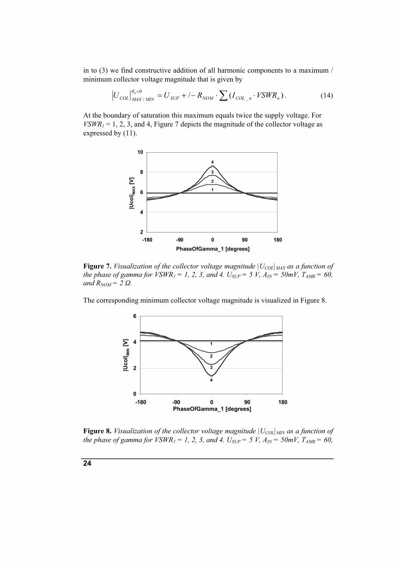
in to (3) we find constructive addition of all harmonic components to a maximum / minimum collector voltage magnitude that is given by
)(/ _0
/ ∑ ⋅⋅−+==nnCOLNOMSUPMINMAXCOL VSWRIRUU nθ
. (14)
At the boundary of saturation this maximum equals twice the supply voltage. For VSWR1 = 1, 2, 3, and 4, Figure 7 depicts the magnitude of the collector voltage as expressed by (11).
2
4
6
8
10
-180 -90 0 90 180
|Uco
l| MA
X [V
]
PhaseOfGamma_1 [degrees]
4
3
2
1
Figure 7. Visualization of the collector voltage magnitude |UCOL|MAX as a function of the phase of gamma for VSWR1 = 1, 2, 3, and 4. USUP = 5 V, AIN = 50mV, TAMB = 60, and RNOM = 2 Ω.
The corresponding minimum collector voltage magnitude is visualized in Figure 8.
0
2
4
6
-180 -90 0 90 180
|Uco
l| MIN
[V]
PhaseOfGamma_1 [degrees]
4
3
2
1
Figure 8. Visualization of the collector voltage magnitude |UCOL|MIN as a function of the phase of gamma for VSWR1 = 1, 2, 3, and 4. USUP = 5 V, AIN = 50mV, TAMB = 60,

25
and RNOM = 2 Ω.
In conclusion, according to (11) the maximum and minimum collector voltage magnitudes increase with increasing supply voltage USUP and, via the collector current ICOL_1, with increasing signal amplitude AIN. Under mismatch, the minimum and maximum collector voltage magnitude are most extreme at a mismatch phase of zero degrees. At zero degrees mismatch the maximum collector voltage magnitude increases with increasing VSWR, whereas the minimum decreases with VSWR.
2.4.3 Die temperature fluctuation Power amplifier die temperature is important because over-heating potentially
causes thermal run-away of the device. Therefore, in this Section we derive the operating conditions at which the die temperature is most extreme.
The average die temperature TDIE can be expressed as a function of the ambient temperature TAMB, the thermal resistance RTH, and the dissipated power, that equals the difference between the DC power delivered by the supply PSUP and AC power delivered to the load PLOAD_n.
)( _ nLOADSUPTHAMBDIE PPRTT −⋅+= . (15)
The supply power is given by
DCCOLSUPSUP IUP _⋅= , (16)
and the power delivered to the load by
∑ ℜ⋅= )21( _
2__ nLOADnCOLnLOAD ZIP . (17)
From (5) and (6) we can express the real part of the load impedance as
nnn
nNOMnLOAD RZ
θcos21
1 2
2
_Γ−Γ+
Γ−=ℜ . (18)
Substitution of (16), (17), and (18) in to (15) yields for the die temperature
)]cos21
121(
[
2
22
_
_
∑Γ−Γ+
Γ−−
+=
nnn
nNOMnCOL
DCCOLSUPTHAMBDIE
RI
IURTT
θ
, (19)
while the magnitude of the collector currents are a function of AIN/UT as given by (2a) to (2d). By taking the derivatives to θn, we find that for θn = +/-π maximums in die temperature occur that are given by

26
)]121(
[
2_
__
nNOMnCOL
DCCOLSUPTHAMBMAXDIE
VSWRRI
IURTTn
∑−
+=±= πθ
. (20)
Similarly, for θn = 0 minima in die temperature are found that are given by
]21[ 2
__
0_
nNOMnCOLDCCOLSUPTH
AMBMINDIE
VSWRRIIUR
TTn
∑−
+==θ
. (21)
Figure 9 depicts the die temperature as expressed by (19) for VSWR1 = 1, 2, 3, and 4.
70
80
90
100
-180 -90 0 90 180
T DIE
[C]
PhaseOfGamma_1 [degrees]
4
3
2
1
Figure 9. Visualization of the die temperature TDIE as a function of the phase of gamma for VSWR1 = 1, 2, 3, and 4. USUP = 5 V, AIN = 50mV, TAMB = 60, and RNOM = 2 Ω, while RTH = 30 K/W.
In conclusion, according to the equations (17) and (18), a maximum in die temperature is found at a mismatch phase of +/-180 degrees, because minimum power is delivered to the load (lowest load resistance), while the power supplied remains constant for a constant input signal AIN.
Moreover, according to (19) the die temperature is linear proportional to the supply voltage.
2.4.4 Efficiency fluctuation In this Section, we describe the impact of fluctuations in environment on the efficiency of a power amplifier, which is one of its most important specifications.

27
The efficiency η of a power transistor is usually defined as the ratio between the power delivered to the load at the fundamental frequency PLOAD_1 and the DC power delivered by the supply PSUP, like
%1001_ ⋅=SUP
LOAD
PP
η . (22)
Substitution of (16) and (17) yields
%100
21
_
1_2
1_⋅
⋅
ℜ⋅=
DCCOLSUP
LOADCOL
IU
ZIη . (23)
Further substitution of (2a), (2b), and (18) gives
%100...
641
411
...)81(
cos21
121
4
4
2
2
23
3
112
1
21
+++
++
Γ−Γ+
Γ−=
T
IN
T
IN
T
IN
T
IN
SUP
NOM
UA
UA
UA
UA
UR
θη . (24)
Figure 10 shows the die temperature as a function of mismatch.
0
10
20
30
40
-180 -90 0 90 180
Eff [
%]
PhaseOfGamma_1 [degrees]
4
3
2
1
Figure 10. Visualization of the efficiency as a function of the phase of gamma for VSWR1 = 1, 2, 3, and 4. USUP = 5 V, AIN = 50mV, TAMB = 60, and RNOM = 2 Ω.
In conclusion, according to (24), the efficiency has a maximum for a mismatch phase of zero degrees, and increases with increasing VSWR. The amplifier efficiency is inverse proportional the supply voltage. The efficiency increases with increasing input signal amplitude AIN because the current ICOL_1 , in (23), increases more rapidly than the current ICOL_DC, as derived in Section 2.4.1.

28
2.4.5 Discussion on the impact of variables From the analysis above we can summarize (for a constant input signal amplitude)
the worst case operating conditions as follows: • The collector voltage is most extreme at a mismatch phase of zero degrees.
For this condition: o The maximum collector voltage magnitude is most extreme at
maximum supply voltage, which potentially gives rise to avalanche breakdown.
o The minimum collector voltage magnitude is most extreme at minimum supply voltage, potentially causing distortion due to clipping.
• Power dissipation is highest at a mismatch phase of +/- 180 degrees, and at maximum supply voltage, which potentially causes thermal run-away.
These conclusions are visualized in Figure 11.
PhaseOfGamma [degrees]
USUP [V]
3
5
4
0-180 +180
Highest |UCOL|MAXAvalanchebreakdown
Lowest |UCOL|MINDistortion
Highest PDISSThermal
run-away
Highest PDISSThermalrun-away
Nominalconditions
Figure 11. Worst case operating conditions causing undesired behaviours that need to be avoided.
For the sake of mathematical simplicity, the analysis is performed on a non-
saturated power amplifier. For a saturated PA, however, all trends are similar, but the impacts are more pronounced. Since saturation limits the average current flowing through the power transistor, a relatively small collector current will flow at zero degrees mismatch and low supply voltage, whereas a relatively large current will flow at +/- 180 degrees mismatch and high supply voltage. Hence, more severe distortion will occur in the first case, whereas more power will be dissipated in the latter.
29
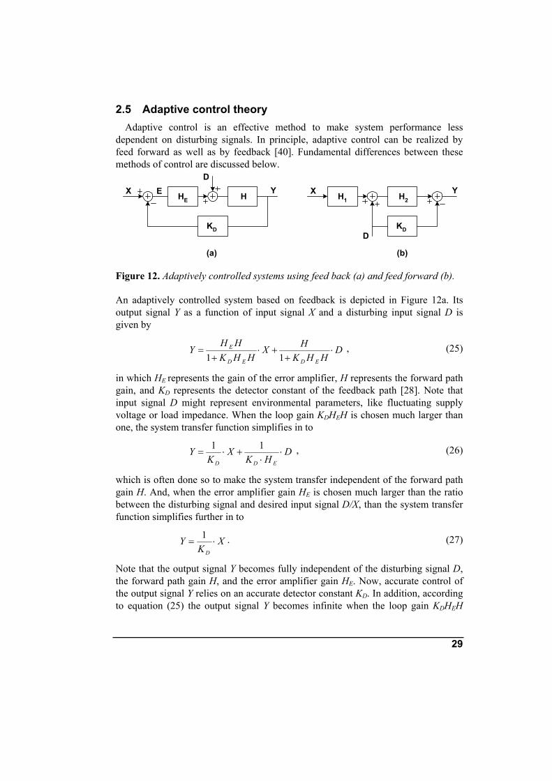
2.5 Adaptive control theory Adaptive control is an effective method to make system performance less
dependent on disturbing signals. In principle, adaptive control can be realized by feed forward as well as by feedback [40]. Fundamental differences between these methods of control are discussed below.
(a) (b)
HX YD
HEE
KD
H2X Y
D
H1
KD
Figure 12. Adaptively controlled systems using feed back (a) and feed forward (b).
An adaptively controlled system based on feedback is depicted in Figure 12a. Its output signal Y as a function of input signal X and a disturbing input signal D is given by
DHHK
HXHHK
HHY
EDED
E ⋅+
+⋅+
=11
, (25)
in which HE represents the gain of the error amplifier, H represents the forward path gain, and KD represents the detector constant of the feedback path [28]. Note that input signal D might represent environmental parameters, like fluctuating supply voltage or load impedance. When the loop gain KDHEH is chosen much larger than one, the system transfer function simplifies in to
DHK
XK
YEDD
⋅⋅
+⋅=11 , (26)
which is often done so to make the system transfer independent of the forward path gain H. And, when the error amplifier gain HE is chosen much larger than the ratio between the disturbing signal and desired input signal D/X, than the system transfer function simplifies further in to
XK
YD
⋅=1 . (27)
Note that the output signal Y becomes fully independent of the disturbing signal D, the forward path gain H, and the error amplifier gain HE. Now, accurate control of the output signal Y relies on an accurate detector constant KD. In addition, according to equation (25) the output signal Y becomes infinite when the loop gain KDHEH

30
equals –1, which illustrates that for feed back systems stability of the loop is important.
For a feed forward based adaptively controlled system, shown in Figure 12b, we
can describe the transfer function in a similar manner. The output signal Y as a function of input signal X and disturbing signal D is given by
DKHXHHY D ⋅−+⋅= )( 221 . (28)
In this case, the output signal is proportional to the forward path gain H1H2 for input signal X and becomes independent of disturbing signal D when the detector constant KD equals the gain H2. Hence, for an accurate output signal Y, fully independent of D, both H1 and H2 must be very precise and KD must be exactly equal to H2. Therefore, feed forward can not be applied in controlling systems that need high precision.
In this thesis we make use of control systems that are based on feedback in order
to become insensitive to inaccuracies of the forward path, which is important for the following reasons.
In case of adaptive impedance matching, treated in Chapter 3, small variations in component values can result in large variations of the matching impedance1, especially for high-order matching networks that need to tune over a wide load impedance and frequency range. Especially the accuracy of RF-MEMS capacitors is rather limited, due to variations in dielectric layer thickness, roughness, plate and spring bending, etc. In addition, parasitic capacitors and inductors of the components and that of interconnect usually have a large impact on the impedance transformation. Fortunately, the antenna impedance varies relatively slowly. Therefore, the gain-bandwidth requirements and thus the requirements on loop stability are rather relaxed.
In case of adaptive power control, treated in Chapter 4, the gain accuracy of the power amplifier that usually consists of multiple RF-stages in a line-up, is limited by the frequency and power dependent impedance matching at its input, inter-stages, and at the output. Since, output power variations occur relatively fast, especially in GSM-mode, gain-bandwidth and loop stability optimization are needed for reliable operation.
In contract to adaptively controlled systems, re-configurable systems make use of a priori knowledge for control. Hence, they do not make use of detection, within the system under consideration.
1 The matching impedance is called the impedance to which the load impedance is being transformed by the
tunable matching network, irrespective of the source impedance.

31
2.6 Identification of variables for detection and correction In this Section we discuss the variables that are most suited for detection and
correction in order to achieve the various goals we are aiming for. Since so many combinations of variables for detection and actuation are thinkable, we follow a top-down approach to categorize the variables and discuss the properties they have in common. Then, the variables from each category will be judged on their usefulness. Figure 13 depicts the environment of a bipolar power transistor and its variables that need to be judged. The figure already suggests that, in practice, adaptive correction can be applied at four different locations: the DC-paths and RF-paths at input and output. Correction of the emitter DC- or RF-path is not realizable without degrading the amplifier performance significantly because the impedance at the emitter is an order of magnitude lower than that at the collector and base.
UBAT
USUP
ZANTPIN
POUT
PTRX
TDIE
UB
UCOL
IB
ICOL
IE
ZLOAD
ISUP
Independent
Singlydependent
Multiplydependent
TAMB
UBIASUREF
IBIAS
Figure 13. Representation of a power transistor environment and its variables that can be used either for detection or actuation
Three main categories of variables can be distinguished: (I) independent variable,
(II) singly dependent variables, and (III) multiply dependent variables. The independent variables can be divided into two groups: a priori known and a priori unknown variables. Each singly dependent variable depends (prior to adaptation) only on one independent variable, whereas each multiply dependent variable depends (prior to adaptation) on more than one independent variable.

32
I. Independent variables • A priori unknown
o Antenna impedance ZANT o Battery voltage UBAT o Ambient temperature TAMB
• A priori known o Power from transceiver PTRX o Bias reference voltage UREF
II. Singly dependent variables
• Load impedance ZLOAD :: f (ZANT) • Supply voltage USUP :: f (UBAT) • Input power PIN :: f (PTRX) • Bias voltage UBIAS :: f (UREF)
III. Multiply dependent variables • Collector voltage UCOL :: f (USUP, ZLOAD, PIN, ..) • Collector current ICOL :: f (USUP, ZLOAD, PIN, ..) • Emitter current IEM :: f (USUP, ZLOAD, PIN, ..) • Die temperature TDIE :: f (USUP, ZLOAD, PIN, TAMB, ..) • Output power POUT :: f (USUP, ZLOAD, PIN, ..) • and many others
2.6.1 Independent variables From a power amplifier point of view the five independent variables ZANT, UBAT,
TAMB, PTRX, and UREF are all inputs to the system. Since we cannot change the operating environment, implicitly, these five independent variables cannot be actuated. Of course, detection of these input signals is very well possible, but it would result in feed forward control, which is not attractive when accurate control is required (see Section 2.5). Table 1 summarizes the adaptive control properties of the independent variables.
In conclusion, the independent variables ZANT, UBAT, TAMB, PTRX, and UREF can not
be actuated and are not very suitable for detection when accurate control is required.

33
Independent variables
Environmental influence Detection Actuation Antenna impedance ZANT ZZZAAA NNN TTT Battery supply voltage UBAT UUUBBB AAA TTT Transceiver output power PTRX TTTAAA MMM BBB Reference voltage UREF PPPTTT RRR XXX Antenna impedance ZANT UUURRR EEE FFF
Independent variables cannot be influenced
Remarks Not accurate
Table 1. Summary on adaptive control of independent variables. The embossed variables are less suitable for adaptation.
2.6.2 Dependent variables 2.6.2.1 Singly dependent variables
The four variables ZLOAD, USUP, PIN, and UBIAS are singly dependent on the corresponding independent variables ZANT, UBAT, PTRX, and UREF respectively, because each singly dependent variable is derived from that corresponding independent variable and is isolated from other independent variables, by the circuit. For instance, the input power PIN is directly related to the power from the transceiver PTRX, but is independent of the supply voltage USUP and load impedance ZLOAD.
Therefore, these singly dependent variables can effectively be used for detection in order to compensate fluctuations of their corresponding independent variables by an actuator that is placed in-between, as is shown in Figure 13.
Singly dependent variables
Environmental influence Detection Actuation Remarks Antenna impedance ZANT ZLOAD ZLOAD 2 dimensional tunable
matching network Battery supply voltage UBAT USUP USUP Series regulator, or
DC/DC converter Transceiver output power PTRX PPPIII NNN PPPIII NNN Varies over a
very wide range Reference voltage UREF UUUBBB III AAA SSS UUUBBB III AAA SSS Usually stabilized Remarks Feed back
Table 2. Summary on adaptive control of singly dependent parameters. The embossed variables are less suitable for adaptation.

34
For instance, the load impedance ZLOAD can be detected in order to correct for variations in antenna impedance by a tuneable impedance matching network. In this manner, all four singly dependent variables can be stabilized, in principle.
Of course, stabilization of the input power PIN is not practical because the PA output power must be variable over a very wide dynamic range. Usually, the bias voltage UBIAS is stable, because it is often determined by a band-gap defined reference voltage UREF. Often, the bias voltage is made temperature dependent in order to compensate for temperature drift of the power transistor.
DC-DC converters are used for supply regulation (and efficiency optimisation) of W-CDMA power amplifiers that have relatively low maximum output power. Despite their lower efficiency, series regulators are used for supply regulation (and power control) of GSM power amplifiers, because the relatively high (pulsed) output power would require a DC-DC converter that is too bulky to fulfil the demanding size requirements of highly miniaturized phones.
Stabilization of the power amplifier load impedance, by adaptive control, is subject of research, nowadays, and is treated in Chapter 3 of this thesis in much detail.
In conclusion, from all single dependent variables ZLOAD and USUP are the most
suited variables for stabilization by adaptive control. 2.6.2.2 Multiply dependent variables
In contrast to singly dependent variables, the multiply dependent variables depend on more than one independent variable. Especially the nodal voltages and branch currents of the bipolar power transistor are multiply dependent variables. Actually in the center of the circuit, depicted in Figure 13, the influences of the various independent (environmental) variables are coming together.
A. Detection
Detection of one of these multiply dependent variables gives no detailed information on the independent variables individually. Hence, the information obtained from detection of a multiply dependent variable cannot be used for accurate compensation of environmental fluctuations and nominal operating conditions for the power transistor cannot be secured.
But, detection of one of these multiply dependent variables, close to the power transistor, does provide detailed information on one of the operating conditions of the power transistor. Since the undesired behaviors, which the power transistors suffer from, are mainly correlated to only one of these multiply dependent variables, detection of only one of these variables provides useful information to avoid such behavior by adaptive control.

35
Table 3 gives an overview of multiply dependent variables that are most suited for detection and single dependent variables that are most suited for correction in avoiding various undesired transistor behaviors.
Since avalanche breakdown is strongly correlated to the collector-base junction
voltage, the power transistor collector voltage UCOL is a suited variable in detecting over-voltage operating conditions of the transistor.
Under avalanche conditions the power transistor base current, and thus the bias current IBIAS, becomes negative. Because of the strong correlation between negative bias current and avalanche breakdown, IBIAS is a suited variable for detection in avoiding avalanche breakdown.
Thermal run-away is directly related to dissipated power. Therefore, the multiply dependent variable die temperature TDIE is suited in detecting over-heating conditions of the power transistor.
Interconnect blow-out is directly related to the currents flowing through the power transistor. Hence, the multiply dependent variables ISUP, ICOL, and IEM are suited in detecting over-current conditions.
Distortion due to saturation is strongly correlated to the collector voltage. The multiply dependent variable UCOL is well suited in detecting under-voltage conditions of the power transistor.
Information on reduced maximum output power can best be obtained from detection of the output power POUT itself. Detecting collector voltage information only or collector current information only is less suited because the correlation with the actual output power is weak.
B1. Actuation of multiply dependent variables In principle, multiply dependent variables can also be used for actuation. In
practice, however, the power transistor performance is very sensitive to circuit parasitics, which poses severe limitations on the design of actuator circuits close to the power transistor.
B2. Actuation of singly dependent variables Actuation of one of the singly dependent variables is more practical, because the
actuator circuit is more isolated from the power transistor and parasitics of the actuator circuit have less influence on the performance. In this Section we describe a selection of the most suited variable that is based on the required directions of control.
Controlling the supply voltage USUP downwards (D) is effective in avoiding
avalanche breakdown, thermal run-away, and blow-out. But, to avoid distortion due to saturation and to avoid a reduction in maximum output power, the supply voltage must be controlled upwards (U). This contradiction in direction of control makes the supply voltage less suited for actuation.

36
Controlling the load impedance ZLOAD to a lower value is effective in avoiding avalanche breakdown, distortion due to saturation, and reduced maximum output power, but to avoid thermal run-away and blow-out, the load impedance needs to be increased. Hence, there is a similar contradiction in direction of control of ZLOAD, which makes it less suited for actuation.
The biasing voltage UBIAS is unsuited for actuation, because, at high power, the currents of a class-AB power transistor are determined by self-biasing due to RF and not by the biasing applied from the external reference voltage UREF.
Controlling the input power PIN downwards is effective in avoiding all undesired behaviors, except for the maximum output power that reduces.
In conclusion, actuation of the power transistor input power is most suited in
avoiding undesired transistor behavior, while information, correlated to undesired behavior, is obtained from detection of one or more multiply dependent variables. Adaptive power control is treated in Chapter 4 of this thesis in more detail.
Multiply dependent variables
Problem Detection Actuation UUUSSS UUU PPP ZZZLLL OOO AAA DDD UUUBBB III AAA SSS PIN
UCOL Avalanche breakdown IBIAS
D D
D D
Thermal run-away
TDIE D U D D
Blow-out ISUP,ICOL,IEM D U D D Distortion due to saturation
UCOL U D D D
Reduced max. output power
POUT U D U U
Contradiction in
direction of control
Prohibited by self-biasing
Same direction of control, except for POUT
Remarks
2 dim. Easy to implement
Table 3. Summary on adaptive control of multiply dependent variables and the directions of control of correlated singly dependent variables that avoid undesired transistor behaviour. D means Downwards and U Upwards control. The embossed variables are less suitable for correction.

37
2.7 Conclusions on adaptive RF front-ends The performance of the RF front-end – antenna combination of a mobile phone is
important to the quality of the wireless link between hand-set and cellular network base-stations. Fluctuations in the mobile phone environment have strong impact on the RF front-end performance.
A theoretical analysis on the relationships between these environmental variables and the main properties of a power amplifier reveals that:
• The collector voltage is most extreme at a mismatch phase of zero degrees. For this condition:
o The maximum collector voltage magnitude is most extreme at maximum supply voltage, which potentially gives rise to avalanche breakdown.
o The minimum collector voltage magnitude is most extreme at minimum supply voltage, potentially causing distortion due to clipping.
• Power dissipation is highest at a mismatch phase of +/- 180 degrees, and at maximum supply voltage, which potentially causes thermal run-away.
Feed-back based adaptive control is proposed, to make the RF front-end resilient
to a priori unknown fluctuations in antenna load impedance, supply voltage, and temperature, as well as to spreads in component values, like that of RF-MEMS devices and the RF parasitics of impedance matching networks and power transistors. In a systematic manner, the variables that are most suited for actuation and detection have been identified, as follows:
• Adaptive impedance control, using (complex) impedance detection to stabilize the load impedance
• Adaptive voltage control, using detection of the supply voltage for supply voltage stabilization
• Adaptive power control, using: o Maximum collector voltage detection or negative base current
detection in order to avoid avalanche breakdown of the power transistor
o Minimum collector voltage detection to avoid distortion due to saturation
o Die temperature to avoid over-heating and electro-thermal instability of a bipolar power transistor
o Supply current detection in avoiding interconnect blow-out Adaptive impedance control and adaptive power control are treated in more detail in the following Chapter 3 and 4 respectively.

39
Chapter
3 Adaptive impedance control
3.1 Introduction This Chapter is devoted to adaptive impedance matching techniques that have
been investigated as a means to improve the link quality of mobile phones under fluctuating operating conditions. Adaptive techniques are attractive because they provide resilience to changes in body-effects and phone form factor. In principle, they can preserve maximum radiated power, power amplifier linearity, receiver sensitivity, and power efficiency of a mobile phone simultaneously.
However, achieving proper adaptive impedance control over a large impedance region is challenging. Matching networks that provide a large tuning region usually exhibit high-order non-linear impedance transformation characteristics that result in multiple solutions and cause non-orthogonal control properties, which hampers robust control. In this introduction, we will explore these challenges in more detail by addressing the following topics:
• 2-dimensional control • Non-linear impedance transfer functions • Multiple solutions • Robust control • Impedance tuning region • Insertion loss • System gain Several solutions to these problems are presented in this Chapter, as summarized
in Figure 14 under Thesis approach. These solutions are treated in an order of reduced impedance tuning region of the networks, and a correspondingly diminishing in network and control complexity.
Firstly, a novel adaptive impedance technique is presented in Section 3.3, which is based on differential control of two capacitors2 for tuning PI- and T-networks. This differential control reduces the number of independent variables to two, which is the
2 The capacitance of a first capacitor increases while that of a second capacitor decreases (both) linearly
proportional in response to a control voltage (or control code).

40
minimum for controlling the two dimensions of impedance (real and imaginary). It provides unique solutions and results in pseudo-orthogonal control of the matching impedance over a relatively wide tuning region.
Secondly, in Section 3.4 a cascade of two loops is proposed for adaptive control of L-networks. This technique provides independent control of the real and imaginary part of the matching impedance. It uses a secondary feedback path to enforce operation in to a stable region, when needed.
Thirdly, an adaptively controlled series-LC network is presented in Section 3.5 that provides a 1-dimensional impedance correction and uses only one variable capacitor.
Adaptive impedance control over a large region
2-dimensional high-order non-linear transfer functionAt least 3 independent variables (capacitors)
Robust control is hampered by:Non-orthogonal control of these 2 dimensionsMultiple solutions (ambiguiety)
Common approachesThesis approach
Functional control techniques:Simplified network tunabilityOrthogonal detection
Gradient Search algorithmComputation based algorithm
Convex Cost Function by mappingDetailed a priori knowledgeneeded (calibration data in LUT)Control of (>) 3 independentvariablesMulti disciplinary
Complex reliable algorithm
Limited a priori knowledge neededon network control propertiesControl of only 2 independentvariables providing pseudo-orthogonal control properties
Simple reliable algorithm
Link quality
Figure 14. Overview on adaptive impedance control techniques.

41
At the start of this thesis work it was envisioned that adaptively controlled antenna impedance matching networks will gradually evolve from fully hardware implemented stand-alone modules towards tuner modules controlled by more advanced algorithms implemented in the firmware of phones. Going along this evolutionary path, the required technologies [41]-[49] for the implementation of very linear tunable elements would need to be developed and optimized in parallel.
For the realization of stand-alone modules, in this thesis work so-called functional control techniques have been explored (see Figure 14 under Thesis approach) because these techniques are well suited for analog and mixed-signal circuit implementations. These functional control techniques make use of a priori knowledge on control properties of tunable LC-networks that are often visualized as rotations over circle segments in a Smith chart. For 2-dimensional functional control techniques detection of the complex values of impedance and admittance is very desirable. Therefore, in Section 3.2 a generic detector is proposed that provides a power and modulation independent orthogonal reading of the real and imaginary part of the impedance, admittance or reflection coefficient.
More commonly used approaches (see Figure 14 under Common approaches) like Gradient Search and software computation based techniques [50]-[53] have not been considered in this thesis, leaving challenges for the future.
3.1.1 Dimensionality Matching of a network can be described in the impedance domain Z, in the
admittance domain Y, as well as in the reflection coefficient domain Γ. In each domain matching is described by a 2-dimensional quantity that can either be represented by a vector in the Polar system or by a complex number in the Cartesian system. See Table 4.
Coordinate system Domain
Polar Cartesian Range
Z ZjeZ ϕ⋅|| XjR ⋅+ || Z ∞..0 Zϕ 90..90 +−
Y YjeY ϕ⋅|| BjG ⋅+ || Y ∞..0 Yϕ 90..90 +−
Γ Γ⋅Γ θje|| ImRe Γ⋅+Γ j || Γ 1..0 Γθ 180..180 +−
Table 4. Domains in which impedance matching can be described in Polar and Cartesian representations.
In more detail, the 2-dimensional impedance Z can be described as a vector with
magnitude |Z| and phase φZ, or as a complex number with a real part R and an imaginary part X, like

42
)sin()cos(|| ZZj ZjZXjReZZ Z ϕϕϕ ⋅+=⋅+=⋅= . (29)
In general, the magnitude of Z ranges from zero to infinite, while the phase of an impedance ranges from –90 to +90 degrees, when we assume the use of physically realizable passive circuits3.
The admittance Y can be described in a similar manner.
1ReΓ
ImΓ
Γ
)cos( Γ⋅Γ θ
)sin( Γ⋅Γ θ
Γθ0
Γ - planeZ - plane
R
X
Z
)cos( ZZ ϕ⋅
)sin( ZZ ϕ⋅
Zϕ0
Figure 15. A Polar and Cartesian representation of the impedance Z and reflection coefficient Γ.
Alternatively, matching can be expressed in terms of wave reflection. The 2-
dimensional reflection coefficient Γ can be described as a vector with magnitude |Γ| and phase θΓ, as well as a complex number with a real and imaginary part, as
)sin()cos(|| ImRe ΓΓ Γ⋅+Γ=Γ⋅+Γ=⋅Γ=Γ Γ θθθ jje j . (30)
The magnitude of Γ ranges from zero to one and the phase of Γ from –180 to +180 degrees, which is distinctly different from the magnitude and phase ranges of Z and Y.
These three domains are related to each other (in a non-linear manner), according
to
Γ−Γ+
⋅==111
0ZY
Z , (31)
in which Z0 is the characteristic impedance to which Γ is normalized. Hence, computation can be used to map the complex numbers from one domain in to the other, as well as to map the numbers from a Polar representation in to a Cartesian representation and vice versa.
Hence, in general adaptive impedance matching requires control in two
3 The impedance of a receiving antenna exhibits a negative real part covering the left-hand-side of the Z-plane

43
dimensions simply because impedance has two dimensions. In special cases however, adaptive impedance matching can be simplified in to 1-dimensional control.
3.1.2 Non-linearity The impedance transformation of a tunable LC ladder networks is non-linear. This
non-linearity, in the two dimensions discussed in the previous Section, can be described by two functions f1 and f2 as power series, like
....
..
..,...),(..
..
..
..,...),(
221232
21222121
2222221
212212120212
221132
21122111
2212211
211211110211
++⋅+⋅+⋅+
+⋅+⋅+
+⋅+⋅+=
++⋅+⋅+⋅+
+⋅+⋅+
+⋅+⋅+=
xxcxxcxxc
xbxb
xaxaaxxf
xxcxxcxxc
xbxb
xaxaaxxf
,
(32)
in which the independent variables x1, x2,.. represent the tunable elements in the network and aij, bij, and cij are constants. The number of terms in the transfer functions f1 and f2 increases with the number of LC-network branches and with the number of elements per branch.
Such a non-linear impedance transformation is well illustrated by the analysis of a
tunable PI-network, shown in Figure 16, performed by Fidler and Thompson in [51].
C1 C2
L
RS
ZM
Figure 16. Tuneable PI-network
They show that for a real source impedance RS the real and imaginary part of the matchable impedance ZM are given by
221
321
22
221 )()1(),,(
SSS
SM RCLCRCRCLC
RLCCR
ωωωω −++−= ,

44
(33)
and
[]
221
321
22
2
22
21
252
2322
21
221
3221
3
21 )()1(
2
),,(SSS
SS
SSS
M RCLCRCRCLCRCCLCLRC
RCLRCLCRLC
LCCXωωωω
ωωω
ωωωω
−++−−−−
−++
= .
(34)
These two equations, representing the impedance transfer functions f1 and f2, reveal that tuning the matching resistance RM by either C1, C2 or L affects XM, and vice versa, which illustrates the non-orthogonal tuning properties over the two dimensions. Further in-sight in the tuning properties of this network is obtained from deriving the matchable impedance for each variable element individually. For constant C2 and L and varying C1, a circular impedance curve is found that is given by:
2
22
2
2
22
2
22
2 )1(2)1()1(2
−
=
−
−−+
−
−LCR
LCLX
LCRR S
MS
M ωωω
ω,
(35)
which center and radius are:
−
−− )1(
,)1(2 2
222
2 LCL
LCRS
ωω
ω, and
− 2
22 )1(2 LC
RS
ω (36)
respectively. Similarly, for constant C1 and L and varying C2, a circular impedance curve is found that is given by
[ ]2
21
221
221
32
22
21
221
221
32
])(1[2)(
])(1[2)(
+
−++
=+
+
−++−
SS
SSS
MSS
SSSM
RCRRCRLCLR
XRCR
RCRLCLRR
ωωωω
ωωωω
. (37)
And finally, for constant C1 and C2, the impedance curve for varying L is given by 2
22
2
221
22
2
2
22
2
221
2
211
21
+=
−+
+−
S
SM
S
SM RC
RCC
XRCRCR
ωω
ωωω
. (38)
These circular impedance curves are shown in Figure 17. Both capacitors are
tuned from 1 to 10 pF and the inductor from 4 to 12 nH, while f = 900MHz.

45
Crossing lines indicate that multiple C1-C2-L combinations provide the same impedance transformation. These multiple solutions do not result in the same insertion loss of the network, however, because of differences in transformation paths (see Section 3.1.5). In addition, solutions that result in component values close to the boundary of their tuning range might get out of range due to load impedance variations.
L
C1
C2
Many C1 C2 L
give same ZM
values
For a fixed L,
combinationstwo C1 C2
give same ZM
Figure 17. PI-network impedance tuning region, visualized as circular curves, for C1 = 1-10 pF, C2 = 1-10 pF, L = 4-12 nH, and f = 900 MHz.
Robust control of the three independent variables to the most desired values
offering the matching impedance ZM is not straight-forward because the real and imaginary part of ZM cannot be controlled independently and multiple solutions exist causing ambiguousness in control4. The next Section treats some aspects of robust control.
4 For the multiple solutions, offering the same matching impedance, the network properties differ in insertion loss
and frequency bandwidth. Since insertion loss and bandwidth can not easily be detected, they can not easily be made part of control criteria unless elaborate network computation is applied.

46
3.1.3 Robust control The purpose of adaptive control can be defined, in general, as minimizing a cost
function J(x), which defines a maximum error of the so-called normed vector space ||e(x)||, as a function of the variable x relative to a disturbance d where d is an element of a domain D.
δ≤∈
=||||
||)(||max)(dxe
DdxJ (39)
In case of impedance control, the error e(x) can be defined, for example, as the difference between a desired reference impedance R and the actually obtained matching impedance, or actuator output function, f(x):
)(:)( xfRxe −= (40)
This error is a function of the control inputs x setting the capacitor values of the network. The disturbance d represents, for instance, the difference between a nominal load impedance (typically 50 Ω) and the actual load impedance. Hence, d represents load mismatch and is an element of a domain D that defines the entire region of load impedances over which the cost function needs to be minimized.
After optimization, the maximum relative error, over the load impedance region D, shall remain smaller than a desired value δ that, for instance, represents an equivalent maximum allowable VSWR.
A set of input signals x defines the input vector X as
,..,,, 321 nxxxxX = , (41)
while the domain of the controller input vector X is defined as the range of values that are bounded by minima XMIN and maximums XMAX
],..,[ MAXMIN XXX = . (42)
These boundaries define the minimum and maximum values of the independent variables x (variable capacitors).
In case of adaptive impedance control the error e(x) is a 2-dimensional vector space. Usually, the error vector space is made a so-called normed vector space ||e(x)||, for which various definitions are possible. Often the Euclidian norm (indicated by the subscript 2) is used, which is defined as
223
22
212 ||...|||||||||| neeeee ++++= , (43)
representing the magnitude of the error vector due to n independent variables. For this Euclidian norm hold true

47
0|||| 2≥e (44)
A similar definition can be used for the disturbance d like
2Im
2Re2 |||||||| ddd += . (45)
in which dRe and dIm describe the real and imaginary part of disturbances in, for instance, load impedance.
To minimize cost functions many different algorithms can be used and each of
them has its own control properties. The main properties of Gradient Search and Direct Control based algorithms are summarized below and discussed in more detail thereafter.
Gradient Search:
• No a priori knowledge is required on the sign of the control curve slope • The region of convergence to a desired solution (A) is bounded by a change in
the Sign of the slope (C) • A Gradient Search diverges (gets stuck) to undesired local minima caused by
non-monotonicity in control, which can be due to: o Matching network tuning characteristic o Variable capacitor control characteristic
• Gradient Search needs more narrow capacitor boundaries to avoid convergence to undesired (local) optima
• Gradient detection is affected by antenna impedance changes between two mismatch measurements. Hence, it requires a relatively fast adaptation rate, which results in higher power consumption.
• Gradient detection needs extra sampling of mismatch information and more memory and computation to determine direction of control
Direct control:
• In the neighborhood of desired optima (A) a priori knowledge is required on the Sign of the control curve slope
• The region of convergence to a desired solution (A) extends over points of changes in Sign of the slope (C) even up to (an undesired) second solution (B)
• The Sign of the error signal is not affected by non-monotonicity in the control curve, which avoids the algorithm to get stuck in local minima
• The Sign of the error signal is not affected by load variations, which allows for a relatively low adaptation rate and results in low power consumption
• More suited for hardware implementation because the algorithm is simple A combination of Direct Control and Gradient Search can be applied, when
desired.

48
Optimization to a minimum error can be achieved by a Gradient Search, which
takes steps proportional to the negative of the gradient towards a local minimum, in an iterative manner. Figure 18 visualizes control of f(x) to R by stepping the independent variable x according to the first-order gradient of || e || either to xA or xB. In this example two stable solutions exist. However, if solution A is preferred over solution B, for instance because of lower network insertion loss, then convergence to the most desired solution is obtain only over the monotone part of f(x) given by xC < x < XMAX.
R
f(x)
0
||e||
x
CONVERGENCE TO A
x x
x1 x3 x5xAx2 x4 x6
AB
CONVERGENCE TO B
xx
C
xMIN xMAX
Figure 18. In case of Gradient Search, the region of convergence in the neighbourhood of A is bounded by the non-monotonicity of f(x) at C, because the direction in controlling x is based on the Sign in gradient of the error || e ||, according to the up/down pointing double lined arrows.
As an alternative to Gradient Search, in this thesis work optimization is achieved
by so-called Direct Control characterized by two distinct aspects. Firstly, optimization to a minimum error is achieved by taking steps proportional to the Sign or the error towards a local minimum. Secondly, control of the networks is simplified in optimization of two 1-dimensional errors simultaneously. In each dimension, the error is made a function of only one independent variable by applying the following techniques:
• Differentially controlled capacitors, in PI- and T-networks, to reduce the number of independent variables
• Cascading two loops for controlling L-networks

49
For the real and imaginary part, the two errors can now be defined as
ReRe|||| ee = (46)
and
ImIm|||| ee = (47)
respectively. Figure 19 visualizes control of f(x) to R by stepping the independent variable x
according to the Sign of error either to xA or to xMIN. Now proper convergence to a desired solution A is achieved for xB < x < XMAX, which extends beyond the monotone region of f(x). For x < XB the system diverges to a boundary given by XMIN.
CONVERGENCE TO A
R
f(x)
0
e xx x
x1 x2 x3xA
A
x
xB
DIVERGENCE
xMAXxMIN
C
B
Figure 19. In case of Direct Control, the region of convergence in the neighbourhood of A extends even to B, because the direction in controlling x is based on the Sign of the error e according to the up/down pointing double lined arrows.

50
The impedance region of robust control is determined by matching network control properties and the chosen control algorithm. This region of robust control can be visualized as the overlapping area between the impedance tuning region of the network and the region of convergence of the algorithm, as shown in Figure 20.
RLOAD
XLOAD
Impedancetuning region
Region ofconvergence
Divergence
Z-plane
Region ofrobust control
Figure 20. A visualization of the impedance tuning region of an LC network and the impedance region of convergence once the network is adaptively controlled. The overlapping area represent a region of robust control.
3.1.4 Impedance tuning region The purpose of a tunable impedance matching network is to transform a relatively
large region of load impedances to a significantly smaller region of matching impedances. Implicitly, as a special case, there is a region of load impedances that can be transformed to an infinitely small region of matching impedances that consists of one impedance point only. Often, the impedance tuning region of a network is defined as the region that can be transformed to such a single point, e.g. 50+0j Ω.
The maximum achievable impedance tuning region is bounded by fundamental properties of the LC network topology and by the component values that are either fixed or variable over a limited range. As an example, Figure 21 illustrates for three different networks the regions of load impedances ZLOAD that can be transformed to a region of matching impedances ZM for which the voltage standing wave ratio VSWRM < 1.5.
Clearly, the PI-network, with three (independent) variable elements, has the largest tuning region in all directions of the two-dimensional Smith chart, but it has the largest number of tunable components.
The (down-converting) L-network covers a smaller impedance region and contains two variable capacitors.
The smallest impedance transformation region is obtained from the series-LC network. Actually, it provides transformation over the imaginary axis only, which is

51
mainly limited to positive reactances. The low complexity of the network, containing only one variable element, is attractive because it is easier to control than the other two networks and its implementation in simpler.
These examples clearly illustrate that for a given capacitance tuning ratio of the variable capacitors the impedance tuning region increases with increased network complexity. In the Section 3.3, 3.4, and 3.5 the properties of these networks will be explored in more detail in conjunction to adaptive control.
ZMZLOAD
ZMZLOAD
ZMZLOAD
Decreasing
tuning region and complexity
(a)
(b)
(c)
Figure 21. Impedance tuning regions of (a) a PI-network, (b) an L-network, and (c) a Series-LC network visualized in Smith charts. The dark grey areas represent a region of load impedances that can be matched to the light grey regions of impedances, for which VSWRM < 1.5. The irregular outer contours are caused by quantization of the variable elements. The tuning ratio of all capacitors is a factor 10 and that of the inductor 3.
3.1.5 Insertion loss Network insertion loss is important because it can partly undo the gain
enhancement obtained from impedance matching. The insertion loss IL of an impedance matching network can be defined as a ratio between dissipated power

52
PDISS and power delivered to the load PLOAD, and is often expressed in dB as
)1log(10LOAD
DISS
PPIL +⋅= . (48)
For a network that consists of a cascade of n series branches and m shunt branches (LC ladder filter topology) this ratio can be expressed as the sum of ratios for each branch
_
_
1_
_
1 jINT
jSHUNTm
jiINT
iSERIESn
iLOAD
DISS
YY
ZZ
PP
ℜ
ℜ+
ℜ
ℜ= ∑∑
==
, (49)
in which ReZSERIES_i and ReYSHUNT_j represent the loss resistance and loss conductance of the series and shunt branches, whereas ReZINT_i and ReYINT_i represent the network resistance and admittance at the intermediate nodes of these branches as depicted in Figure 22.
ZINT_i YINT_j
ZSERIES_i
YSHUNT_jPower
Figure 22. Definition of the intermediate network impedance and admittance of an LC ladder network that consists of series and shunt branches
Consequently, the network insertion loss depends on the impedance path of
transformation along the various nodes of the ladder network. When a network has multiple solutions to provide a desired match, each solution follows a different impedance path that results in a different insertion loss.
Since insertion loss is difficult to detect, it can not easily be used as an optimization criterion for adaptive control. Therefore, optimum solutions needs to be found by using a priori knowledge on the (source and load impedance dependent) insertion loss of the network.
3.1.6 System gain The gain G that can be obtained from applying adaptive impedance matching can
be defined, in dB, as the achievable reduction in reflection loss [57] minus the insertion loss (IL) that is introduced once we apply an adaptive matching network,

53
as
][)||1log(10)||1log(10 22 dBILG LOADM −Γ−⋅−Γ−⋅= , (50)
in which ΓM is the reflection coefficient of the matched port and ΓLOAD that of the mismatched load. Since the magnitude of the reflection coefficient is related to the voltage standing wave ratio as
11||
+−
=ΓVSWRVSWR , (51)
we can rewrite (50), after substitution of (51) in to
][))1()1(
log(10 2
2
dBILVSWR
VSWRVSWRVSWR
GM
LOAD
LOAD
M −+
+⋅⋅= . (52)
Gain contours as a function of load and matching VSWR, according to (52), are depicted in Figure 23. For example, when a load VSWR of 5 is reduced to a matching VSWR of 2 then the gain will be 1 dB, assuming that the network insertion loss is 1 dB.
1
2
3
4
5
6
7
8
9
10
1 2 3 4 5 6 7 8 9 10VSWRLOAD
VSW
RM
G = 0 dB
-2 dB
-4 dB IL = 1 dB
+ 2 dBDEGRADATION
ENHANCEMENT
VSWRLOADVSWRM
ZM
ZLOAD
matchingnetwork
Figure 23. Gain contours as a function of matching and insertion loss. The bold curve represents load and matched conditions for which the gain is 0 dB, for IL = 1 dB.
The bold contour represents matching conditions for which the system gain equals
zero dB. Only at the right hand side of this contour the adaptive matching offers gain enhancements.

54
3.2 Mismatch detection method Measuring mismatch requires sensing of RF information and detection to translate
this sensed RF information to DC. Various methods of RF-sensing and detection are known. Voltage peak detection at two points along a transmission line [58] is elegant, but it gives information on the voltage standing wave ratio (VSWR) only. Voltage peak detection at three nodes gives information on the real and imaginary part of the load impedance, but in a non-orthogonal manner [43], [74], which makes robust control more difficult. A mixer based quadrature detector in conjunction with a VSWR bridge [60], sensing forward and reflected power by means of an directional coupler, only provides information on the reflection coefficient, but not on impedance, nor admittance, without calculations. Moreover, a disadvantage of these three detection methods is the need for additional sensing elements in the RF-path that are lossy, introduce extra parasitic capacitance, and require additional space.
In this Section we describe a generic detector that consists of a classic quadrature detector extended with an amplitude detector and two dividers to provide a power and modulation independent true-orthogonal reading of the real and imaginary part of the impedance, admittance or reflection coefficient.
3.2.1 Sensing Basically, impedance (and admittance) is given by the ratio between voltage and
current. Therefore, we propose to sense voltage and current information [61], as depicted in Figure 24.
SENSEXyxZ =
SENSEXxyY 1
=
Xsenseu i
ux = iXy SENSE ⋅=
1x1x
Figure 24. By sensing voltage u and current i information is obtained on the impedance Z or admittance Y.
The nodal voltage u is measured single-ended, whereas a measure of the branch
current i is obtained from the differential voltage across a sensing element and its reactance XSENSE. This sensing element is typically a fixed inductor (or capacitor)
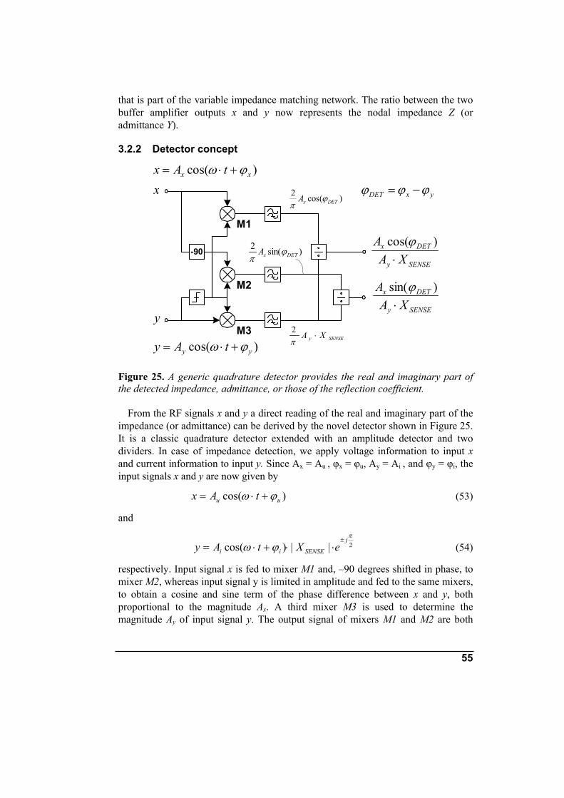
55
that is part of the variable impedance matching network. The ratio between the two buffer amplifier outputs x and y now represents the nodal impedance Z (or admittance Y).
3.2.2 Detector concept
SENSEy
DETx
XAA
⋅)cos(ϕ
SENSEy
DETx
XAA
⋅)sin(ϕ
)sin(2DETxA ϕ
π
SENSEy XA ⋅π2
)cos(2DETxA ϕ
π
-90
)cos( xx tAx ϕω +⋅=
)cos( yy tAy ϕω +⋅=
yxDET ϕϕϕ −=
M1
M2
M3
x
y
Figure 25. A generic quadrature detector provides the real and imaginary part of the detected impedance, admittance, or those of the reflection coefficient.
From the RF signals x and y a direct reading of the real and imaginary part of the
impedance (or admittance) can be derived by the novel detector shown in Figure 25. It is a classic quadrature detector extended with an amplitude detector and two dividers. In case of impedance detection, we apply voltage information to input x and current information to input y. Since Ax = Au , φx = φu, Ay = Ai , and φy = φi, the input signals x and y are now given by
)cos( uu tAx ϕω +⋅= (53)
and
2||)cos(π
ϕωj
SENSEii eXtAy±
⋅⋅+⋅= (54)
respectively. Input signal x is fed to mixer M1 and, –90 degrees shifted in phase, to mixer M2, whereas input signal y is limited in amplitude and fed to the same mixers, to obtain a cosine and sine term of the phase difference between x and y, both proportional to the magnitude Ax. A third mixer M3 is used to determine the magnitude Ay of input signal y. The output signal of mixers M1 and M2 are both

56
divided by the output signal of mixer M3 to obtain the detected impedance ZDET, that can now be expressed as
DETDETDET jXRZ += (55)
in which
SENSEi
DETuDET XA
AR⋅
=)cos(ϕ
, (56)
SENSEi
DETuDET XA
AX⋅
=)sin(ϕ
, (57)
and
iuDET ϕϕϕ −= . (58)
According to the equations (56) and (57) the detected values are inverse proportional to a frequency dependent XSENSE, which implies a need for frequency compensation when high accuracy is desired over a wide frequency range.
Since the detected values are proportional to the ratio Au/Ai, they are independent of the magnitude of the transmitted RF signal. In addition, according to (58) φDET is given by the phase difference between φu and φi and therefore, the detected values are independent of the phase of the RF signal. Hence, the detected real and imaginary part are, in principle, independent of amplitude and phase modulation of the RF signal, which is usually applied.
The detector accuracy, desired over a large output power range and a large load impedance region, is mainly determined by the finite gain of the limiter and its amplitude dependent phase delay, which needs to be traded off versus power consumption. Fortunately, to save power, the detector can be operated at a low ON/OFF duty-cycle (<1%) because the detector settling time is typically very short (10..100 µs) compared to the slow variations (0.1..1 s) in antenna impedance. Hence, the detector bias current will be negligible compared to the quiescent current of a power amplifier.
Since the detector is not frequency selective, it is vulnerable to signals that are being received during transmission. When these received signals are larger than the transmitted signal, the net energy flow changes direction and the detector reads the network impedance seen into the opposite direction. Fortunately, at low output power (< 0 dBm) there is no benefit from adaptive impedance matching and the detector can be turned OFF to avoid incorrect control.
The same detector circuit provides the real and imaginary part of the admittance
by exchanging the two detector input signals x and y. Alternatively, the detector gives a reading of the reflection coefficient Γ when the input signals x and y represent the reflected and incident power waves that, for instance, can be obtained

57
from a directional coupler used as sensing element. Hence, this generic detector provides the complete information of the complex parameters Z, Y or Γ. In special cases however, partial information on those parameter can be sufficient for proper control and simplified versions of the detector can be applied, as exemplified in Section 3.5.
3.2.3 Simulation results Simulation results on the detector (see Figure 25) and its RF sensor (see Figure
24), described by behavioral models, are depicted in Figure 26. It shows the real and imaginary part of the detected impedance for a 50 Ω load with a VSWR of 1, 2, 3, and 4, swept over all phases.
-100
-50
0
50
100
0 50 100 150 200RDET [Ω]
X DET [
Ω]
4
32
1
Figure 26. Detected impedance as a function of load impedance. RNOM = 50 Ω, VSWR = 1, 2, 3, and 4, all phases.

58
3.2.4 Conclusions on mismatch detection
• A novel true-orthogonal detector concept is presented, which provides the real and imaginary part of impedance, admittance, or reflection coefficient.
• The detector output is power and modulation independent. • The detector uses a reactance (inductor or capacitor) for voltage and
current sensing or a directional coupler for sensing incident and reflected waves. The sensing reactance can be a (re-used) matching network element, providing reduced losses, and savings in size and cost.
• The sensed current is a function of the value of the sensing reactance,
which necessitates calibration for high accuracy.
• The average detector power consumption can be low, because the detector can be operated at a low ON/OFF duty-cycle.

59
3.3 Adaptively controlled PI-networks using differentially controlled capacitors
In this Section we present a novel adaptive matching technique that is based on differential control of two capacitors, as shown in Figure 27 applied to a tunable PI-network. This differential control reduces the number of independent variables to two, which is the minimum for controlling the two dimensions of impedance (real and imaginary). It provides unique solutions for the matching impedance ZM and results in pseudo-orthogonal control of the real and imaginary part of the matching impedance over a relatively wide tuning region. Hence, the network can be controlled reliably by a very basic algorithm.
L
CIN,COUT
ZLOADCOUT
CIN
L ZM
Figure 27. Differentially controlled PI-network and its impedance tuning region for ZLOAD = 50 Ω. CIN = 1 .. 10pF, COUT = 10 .. 1 pF, L = 3 .. 12 nH, and f = 870 MHz.
In [74], similar orthogonal tuning properties are strived for using a well
characterized Maury load-pull tuner and a PC emulating a tunable real-to-real impedance transformer.
Usually PI-networks are controlled by computation based gradient search algorithms [50]-[53]. Often, these algorithms need factory calibration data or circuit design information, commonly stored in a large Look-Up-Table, to provide reliable convergence to desired optima. In contrast, the algorithm used in this work simply uses the signs of the errors signals as inputs to Up/Down counters for iterative control of switched capacitor arrays [63], which simplifies its software and/or hardware implementation significantly. If desired, this algorithm can easily be implementation with basic mixed analog/digital building blocks enabling autonomous operation of an adaptive antenna matching module, which application requires only minor modifications of a mobile phone RF front-end and its firmware.
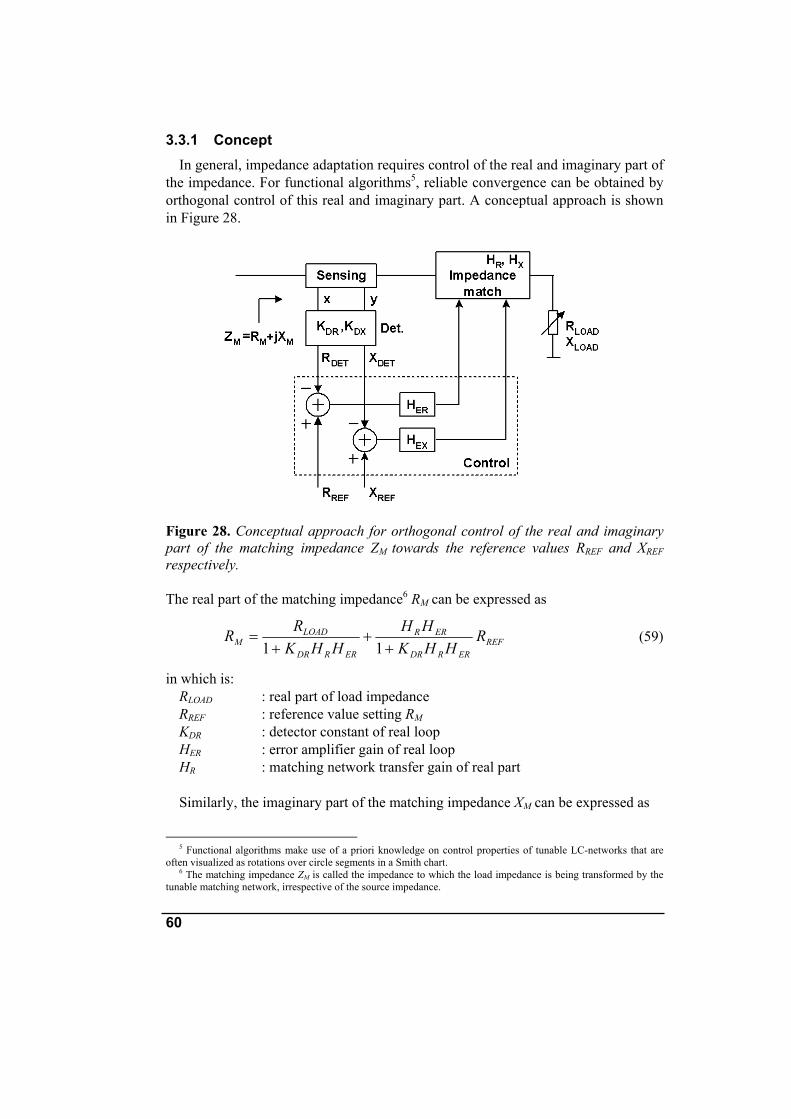
60
3.3.1 Concept In general, impedance adaptation requires control of the real and imaginary part of
the impedance. For functional algorithms5, reliable convergence can be obtained by orthogonal control of this real and imaginary part. A conceptual approach is shown in Figure 28.
Figure 28. Conceptual approach for orthogonal control of the real and imaginary part of the matching impedance ZM towards the reference values RREF and XREF respectively. The real part of the matching impedance6 RM can be expressed as
REFERRDR
ERR
ERRDR
LOADM R
HHKHH
HHKRR
++
+=
11 (59)
in which is: RLOAD : real part of load impedance RREF : reference value setting RM KDR : detector constant of real loop HER : error amplifier gain of real loop HR : matching network transfer gain of real part Similarly, the imaginary part of the matching impedance XM can be expressed as
5 Functional algorithms make use of a priori knowledge on control properties of tunable LC-networks that are
often visualized as rotations over circle segments in a Smith chart. 6 The matching impedance ZM is called the impedance to which the load impedance is being transformed by the
tunable matching network, irrespective of the source impedance.

61
REFEXXDX
EXX
EXXDX
LOADM X
HHKHH
HHKXX
++
+=
11 (60)
in which:
XLOAD : imaginary part of load impedance XREF : reference value setting XM KDX : detector constant of imaginary loop HEX : error amplifier gain of imaginary loop HX : matching network transfer gain of imaginary part The first terms in (59) and (60) represent static errors of both loops, whereas the
second terms represent the wanted terms proportional to the applied references RREF and XREF respectively. For large error amplifier gains HER and HEX these static errors are small and the real and imaginary part of the matching impedance are approx. given by
REFDR
M RK
R 1= (61)
and
REFDX
M XK
X 1= (62)
respectively. Hence, the matching impedance becomes independent of the load impedance.
In stead of using the impedance domain, compensation of mismatch can also be described in the admittance or reflection coefficient domain. In all three cases there is a need for detection of complex values, which is discussed in Section 3.2.
3.3.2 Differentially controlled single-section PI-network In this Section we derive the tuning properties of a PI-network with differentially
controlled capacitors using impedance-to-admittance and admittance-to-impedance transformations.
For the analysis of this differentially controlled PI-network we express shunt branches as admittances and series branches as impedances. Fixed values BC and XL, coming from above in Figure 29, define the nominal operating point of the network. The variable parameters ∆BC and ∆XL represent tuning of the elements. Differential control of the input and output capacitor is defined by opposite signs of ∆BC. Using the signal flow-graph representation, we can now easily derive the matching admittance YM as a function of the element values and load admittance YLOAD.
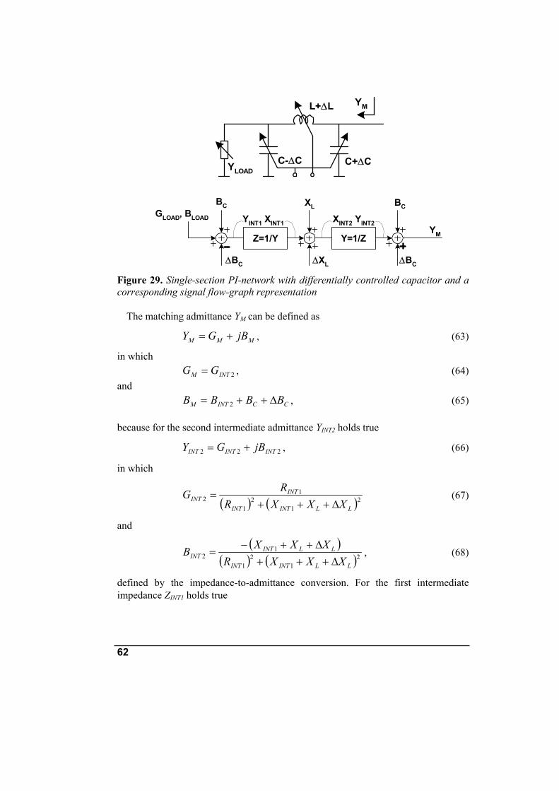
62
YLOADC+∆CC-∆C
L+∆L YM
YM
BC XLGLOAD, BLOAD
Z=1/Y Y=1/Z
BC
∆XL∆BC ∆BC
XINT1 XINT2YINT1 YINT2
Figure 29. Single-section PI-network with differentially controlled capacitor and a corresponding signal flow-graph representation
The matching admittance YM can be defined as
MMM jBGY += , (63)
in which
2INTM GG = , (64) and
CCINTM BBBB ∆++= 2 , (65) because for the second intermediate admittance YINT2 holds true
222 INTINTINT jBGY += , (66)
in which
( ) ( )21
21
12
LLINTINT
INTINT XXXR
RG∆+++
= (67)
and
( )( ) ( )2
12
1
12
LLINTINT
LLINTINT XXXR
XXXB∆+++
∆++−= , (68)
defined by the impedance-to-admittance conversion. For the first intermediate impedance ZINT1 holds true

63
( ) ( )221CCLOADLOAD
LOADINT BBBG
GR∆−++
= . (69)
( )( ) ( )221
CCLOADLOAD
CCLOADINT BBBG
BBBX∆−++
∆−+−= , (70)
defined by the admittance-to-impedance conversion. Substitution yields awkward expressions for GM and BM. Once we normalize the impedance and frequency7, by choosing
11==
LC X
B , (71)
and further simplify the problem8, by choosing
1=LOADG and 0=LOADB , (72)
substitution and rewriting gives
))1(1()1()1)(1(211
22CLCL
M BXBXG
∆−+∆++∆−∆+−= (73)
and
)1())1(1()1()1)(1(21
))1(1)(1()1(22
2
CCLCL
CLCM B
BXBXBXBB ∆++
∆−+∆++∆−∆+−∆−+∆+−∆−
= . (74)
After expansion of these expressions, we can collect equal terms in the nominator and denominator and, for small values of ∆BC and ∆XL, we can ignore all 2nd and higher order small terms, which results in
)21(1
LM X
G∆+
≈ (75)
and
CL
LCM B
XXBB ∆=
∆+∆+∆
≈)21(
)21( . (76)
Hence, by approximation, control of the real and imaginary part of the matching admittance is orthogonal. The matching conductance GM is inversely proportional to reactance variations of the tunable series inductor and is independent of susceptance variations of the differentially controlled shunt capacitors. Similarly, the matching
7 Normalization, or scaling, of impedance and frequency is done without losing generality 8 The network tuning region is given by the matching impedance when the network is loaded by the normalized
impedance 1+0j .

64
susceptance BM is proportional to susceptance variations of the differentially controlled capacitors and is independent of reactance variations of the series inductor.
The real and imaginary part of the matching admittance as a function of variations in capacitor susceptance and inductor reactance, according to (73) and (74) are visualized in Figure 30. Around the normalized admittance 1+0j, small variations in ∆XL and ∆BC result mainly in changes of the real and imaginary part respectively. Moreover, the figure illustrates that each combination of ∆XL and ∆BC provides a unique value for the matching admittance, which reduces the algorithm complexity required for adaptive control.
-3
-2
-1
0
1
2
3
0 1 2 3 4 5 6GM [1/Ω]
BM
[1/Ω
]
∆XL =-0.75
∆XL =0.75
∆ΒC =-0.95
∆ΒC =0.95
∆BC
∆XL
Figure 30. Normalized matching admittance YM of a differentially controlled PI-network, for
∆BC = -0.95, 0.75, -0.5, -0.25, 0 , 0.25, 0.5, 0.75, 0.95 and ∆XL = -0.75, -0.7, -0.6, -0.5, -0.4, -0.2, 0, 0.2, 0.4, 0.5, 0.75. YLOAD =1.
This single-section PI-network needs a variable inductance. Since variable
inductors with a large tuning range can not easily be realized, the variable inductance might be implemented as a fixed inductor in series with (or in parallel to) a variable capacitor. Unfortunately, the equivalent Q-factor of such a composed branch is relatively low and therefore the insertion loss of this single-section PI-network is rather high. In the next Section we discuss a dual-section PI-network that uses fixed inductors and variable capacitors in shunt configuration.

65
3.3.3 Differentially controlled dual-section PI-network Similar pseudo-orthogonal tuning properties can be obtained with a dual-section
PI-network topology that consists of two fixed series inductors and three variable capacitors in shunt configuration as depicted in Figure 31.
YLOAD
C+∆Ck(C-∆C)
L YML
CM+∆CM
YM
BC XLGLOAD, BLOAD
Z=1/Y Y=1/Z
BC
∆ΒCM∆BC ∆BC
XINT1 XINT2BCM
Z=1/Y
YINT3YINT2
Y=1/Z
XINT4 YINT4XLXINT3
Figure 31. Dual-section PI-network with differentially controlled capacitors and fixed inductors and its corresponding signal flow-graph representation
Differential control of the input and output capacitor changes primarily the matching susceptance BM, whereas control of the capacitor in the middle CM changes mainly the matching conductance GM. Using the signal flow-graph representation we can derive the network tuning properties in a similar manner, but it results in high-order functions that do not provide much insight. Therefore, ADS [62] circuit simulations are used to generate Figure 32, which shows the normalized real and imaginary part of the matching admittance as a function of the differential controlled susceptance ∆BC of input and output capacitor and the controlled susceptance ∆BCM of the capacitor in the middle, for a nominal load admittance of 1+0j. For small deltas the tuning is orthogonal, similar to that of a single-section PI-network.

66
-1,5
-1
-0,5
0
0,5
1
1,5
0 0,5 1 1,5 2 2,5 3 3,5
GM [1/Ω]
BM
[1/Ω
]
∆BCM ∆ΒC
Figure 32. Normalized matching admittance of a dual-section PI-network with differentially controlled input and output capacitor
In principle, similar control properties can be achieved with differentially
controlled T-networks. Appendix A gives an overview of adaptively controlled single- and dual-section PI- and T-networks in low-pass and high-pass configurations.
3.3.4 Simulations
3.3.4.1 Adaptive impedance matching
Simulations on adaptively controlled PI-networks have been performed to optimize their performance and to verify convergence behavior. A single-section 900 MHz PI-network has been modeled with differentially controlled CIN and COUT variable from 1 to 10 pF and 10 to 1 pF respectively. The series branch consists of a 4.5 nH inductor in parallel to a 0.5 to 5 pF variable capacitor. The simulation bench includes a 2 nH sense inductor, a complex admittance detector, and a control block. Similarly, a 900 MHz dual-section network has been modeled with differentially controlled CIN (variable from 0.5 to 5 pF) and COUT (variable from 10 to 1 pF). The capacitor CM is made tunable from 0.5 to 5 pF. These tuning ranges are chosen since they are representative for RF-MEMS switched capacitor arrays [63]. Figure 33 and Figure 34 show applied load impedances for VSWRLOAD = 1, 3, 5, and 9, and their corresponding matching impedances ZM obtained after acquisition of the loops of a single-section and a dual-section PI-network respectively.
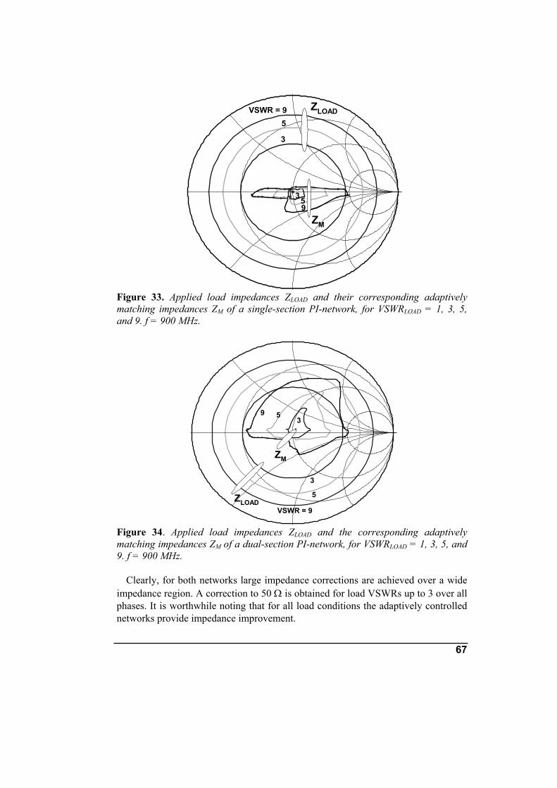
67
ZLOAD
ZM
VSWR = 9
3
5
359
Figure 33. Applied load impedances ZLOAD and their corresponding adaptively matching impedances ZM of a single-section PI-network, for VSWRLOAD = 1, 3, 5, and 9. f = 900 MHz.
ZLOAD
ZM
VSWR = 9
3
5
359
Figure 34. Applied load impedances ZLOAD and the corresponding adaptively matching impedances ZM of a dual-section PI-network, for VSWRLOAD = 1, 3, 5, and 9. f = 900 MHz.
Clearly, for both networks large impedance corrections are achieved over a wide
impedance region. A correction to 50 Ω is obtained for load VSWRs up to 3 over all phases. It is worthwhile noting that for all load conditions the adaptively controlled networks provide impedance improvement.
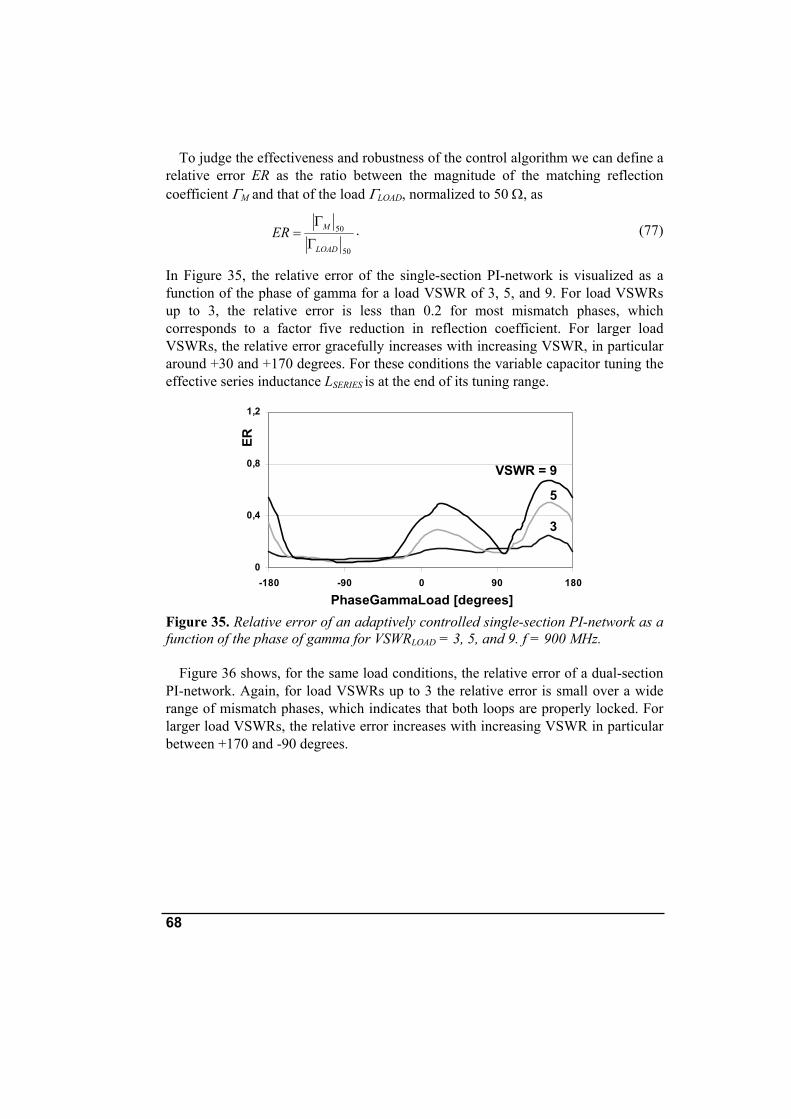
68
To judge the effectiveness and robustness of the control algorithm we can define a
relative error ER as the ratio between the magnitude of the matching reflection coefficient ΓM and that of the load ΓLOAD, normalized to 50 Ω, as
50
50
LOAD
MERΓ
Γ= . (77)
In Figure 35, the relative error of the single-section PI-network is visualized as a function of the phase of gamma for a load VSWR of 3, 5, and 9. For load VSWRs up to 3, the relative error is less than 0.2 for most mismatch phases, which corresponds to a factor five reduction in reflection coefficient. For larger load VSWRs, the relative error gracefully increases with increasing VSWR, in particular around +30 and +170 degrees. For these conditions the variable capacitor tuning the effective series inductance LSERIES is at the end of its tuning range.
0
0,4
0,8
1,2
-180 -90 0 90 180
PhaseGammaLoad [degrees]
ER
VSWR = 9
3
5
Figure 35. Relative error of an adaptively controlled single-section PI-network as a function of the phase of gamma for VSWRLOAD = 3, 5, and 9. f = 900 MHz.
Figure 36 shows, for the same load conditions, the relative error of a dual-section
PI-network. Again, for load VSWRs up to 3 the relative error is small over a wide range of mismatch phases, which indicates that both loops are properly locked. For larger load VSWRs, the relative error increases with increasing VSWR in particular between +170 and -90 degrees.

69
0
0,4
0,8
1,2
-180 -90 0 90 180PhaseOfGamma [degrees]
ERVSWR = 9
3
5
Figure 36. Relative error of an adaptively controlled dual-section PI-network as a function of the phase of gamma for VSWRLOAD = 3, 5, and 9. f = 900 MHz.
3.3.4.2 Insertion loss
The presented simulation results include network insertion losses that are modeled as equivalent series resistors defined by the Q-factors of the network elements. For the fixed series inductors we have chosen QL_SERIES = 50, which is representative for solenoid wire wounded coils. For the variable capacitors in series and shunt branches we have chosen QC_SERIES = 35 and QC_SHUNT = 50 respectively. The equivalent Q-factor of a shunt capacitor can typically be made higher than that of a series capacitor because for the former, biasing resistors are loading the RF signal path less, once biasing is applied at the RF-grounded side. The actual Q-factors depend on the technology used for implementation of the variable capacitors and fixed inductors and varies over frequency and component value.
0
2
4
6
-180 -90 0 90 180
PhaseGammaLoad [degrees]
IL [d
B]
VSWR = 9
3
1
Figure 37. Insertion loss of an adaptively controlled single-section PI-network as a function of the phase of gamma for VSWRLOAD = 1, 3, and 9.

70
0
1
2
-180 -90 0 90 180
PhaseOfGamma [degrees]
IL [d
B] VSWR = 9
3
1
Figure 38. Insertion loss of a dual-section PI-network as a function of the phase of gamma for VSWRLOAD = 1, 3, and 9. The simulated insertion loss as a function of the load mismatch is shown in Figure 37 and Figure 38 for a single- and dual-section PI-network. For a load VSWR of 1 the insertion loss of the single-section PI-network is approximately 0.9 dB, which is predominantly caused by the series branch that is composed of a fixed inductor (Q = 50) in parallel to a variable capacitor (Q = 35). Under mismatch the insertion loss increases, especially for mismatch phases around -30 degrees. The insertion loss of the dual-section PI-network is 0.5 dB, for a load VSWR of 1. Under mismatch conditions the insertion loss increases somewhat, but significantly less than that for the single-section PI-network.
3.3.4.3 System gain
According to (50) in Section 3.1.6, the system gain achieved by applying adaptive impedance matching is simply given by the difference between return loss reduction and insertion loss. For a load VSWR of 1, Figure 39 shows a system gain G of –0.9 dB, which is equal to the network insertion loss, as expected from Figure 37. For a load VSWR of 3, G varies between –1 and +1 dB, which results in a system gain of 0 dB averaged over all mismatch phases. For an extreme VSWR of 9, G varies between 0 and 3.5 dB, with an average value of approximately +1.7 dB.
In comparison, the average system gain of the dual-section PI-network, depicted in Figure 40, is –0.5, +0.5 and +2.2 dB for a load VSWR of 1, 3 and 9 respectively.

71
-2
0
2
4
-180 -90 0 90 180PhaseGammaLoad [degrees]
G [d
B]
VSWR = 9
3
1
Figure 39. System gain of an adaptively controlled single-section PI-network as a function of the phase of gamma for VSWRLOAD = 1, 3, and 9.
-2
0
2
4
-180 -90 0 90 180
PhaseOfGamma [degrees]
G [d
B]
VSWR = 9
3
1
Figure 40. System gain enhancement of a dual-section PI-network as a function of the phase of gamma for VSWRLOAD = 1, 3, and 9.
Clearly, the dual-section PI-network adapts the impedance well over a reasonable
wide impedance region and its insertion loss is relatively small. Hence, its average gain enhancement is about 0.5 dB larger compared to that of a single-section PI-network.
3.3.5 Conclusions on adaptively controlled PI-networks
• A novel adaptive impedance matching technique is presented, using differentially controlled reactances.
• This differential control reduces the number of independent variables to two, which is the minimum for controlling the two dimensions of impedance.
• An analysis on the non-linear impedance transformation characteristics of

72
differentially controlled single-section and dual-section PI-networks is presented.
• This analysis shows that these networks provide unique solutions in impedance transformation and give pseudo-orthogonal tuning properties over a relatively wide tuning region.
• In combination with the true-orthogonal impedance detector applied, robust control is achieved by a simple algorithm that can either be implemented in software or by basic mixed analog/digital circuits.
• Simulations on an adaptively controlled single-section PI-network show a typical system gain of –0.9, 0, and 1.7 dB for a load VSWR of 1, 3 and 9 respectively, averaged over all phases.
• Similar simulations on a dual-section PI-network show a typical system gain of –0.5, 0.5, and 2.2 dB for a load VSWR of 1, 3 and 9 respectively, averaged over all phases.

73
3.4 Adaptively controlled L-network using cascaded loops In this Section we describe an adaptively controlled L-network that consists of
two cascaded loops that provide independent control of the real ands imaginary part of the matching impedance.
3.4.1 Concept A conceptual approach for adaptive control of an L-network is shown in Figure
41. It comprises a cascade of two independent control loops that transforms an unknown load admittance YLOAD to the desired matching impedance ZM given by
MMM jXRZ += . (78)
A first loop controls the parallel capacitor CPAR to set the real part of the matching impedance RM. A second loop controls the series capacitor CSERIES to set the imaginary part of the matching impedance XM .
Figure 41. Conceptual approach for independent control of the real and imaginary part of the matching impedance ZM of an L-network towards the reference values RREF and XREF respectively The intermediate impedance ZINT can be defined as
INTINTINT jXRZ += . (79)
When the first loop is properly locked and the error amplifier gain HER is large, the error signal ER will be small and by approximation holds true
REFDR
INT RK
R 1= , (80)
in which RREF is the reference value setting RM and KDR is the detector constant. Meanwhile, this loop introduces an intermediate reactance XINT. Similarly, when the

74
second loop is properly locked and the error amplifier gain HEX is large, than the error signal EX will be small and by approximation holds true
REFDX
M XK
X 1= , (81)
in which XREF is the reference value setting XM and KDX is the detector constant. Since this second loop does not affect the series resistance, RM equals RINT, and the matching impedance ZM can now be written as
REFDX
REFDR
M XK
jRK
Z 11+= . (82)
Hence, the matching impedance ZM is independent of the load admittance (or impedance), the gain of the error amplifiers, and the matching network component values.
3.4.2 Actuation In this Section we treat some well known properties of series-LC and parallel-LC
tunable networks that are important, because the control techniques presented in Section 3.4.3 are based upon them.
3.4.2.1 Series-LC network
The matching impedance ZM of a series-LC network that is shown in Figure 42 and represents the tunable network of the 2nd loop is defined as
MMM jXRZ += , (83)
in which the matching reactance XM is given by
LOADSERIESCSERIESLM XXXX ++= __ , (84)
and the matching resistance RM by
LOADM RR = . (85)
Tuning the series capacitor value CSERIES changes the matching reactance XM over a circle segment of constant resistance RLOAD as visualized in the Smith chart in bold.

75
RLOAD
XLOAD
ZM
XL_SERIES XC_SERIES
XCOR BM
RLOAD
XM
GM
ZM(CSERIES)
XCOR_IL
XCOR_CL
Figure 42. A variable series-LC network providing correction for inductive and capacitive load reactances visualized on a Smith chart.
The matching reactance XM is a monotone function of the tunable reactance
XC_SERIES, whereas the matching series resistance RM is equal to the load resistance RLOAD and fully independent of the orthogonal reactance XC_SERIES. In adaptive matching networks the monotonicity of the function ZM(CSERIES) is a very desirable property because it results in robust control. Moreover, the orthogonal property of resistance and reactance will be used advantageously in the adaptive-L network to tune the matching reactance to a desired value, without affecting the matching resistance.
3.4.2.2 Parallel-LC network
In analogy to the matching impedance of a series-LC network, the matching admittance YM of a parallel-LC network, as shown in Figure 43 and representing the tunable network of the 1st loop, is defined as
MMM jBGY += (86)
in which the matching susceptance BM is given by
LOADPARCPARLM BBBB ++= __ , (87)
and the matching conductance GM by
LOADM GG = . (88)
Note that the matching admittance YM of this parallel LC-network corresponds to the intermediate admittance YINT of the L-network.
Tuning the parallel capacitor value CPAR changes the matching susceptance BM over a circle segment of constant conductance GLOAD as visualized in the Smith chart.

76
GLOADBLOAD
YM
BL_PAR BC_PAR
BCORXM
GLOAD
BM
RM
YM(CPAR)
BCOR_IL
BCOR_CL
Figure 43. A variable parallel-LC network and its matching admittance YM visualized on a Smith chart.
The matching susceptance BM is a monotone function of the tunable susceptance
BC_PAR, whereas the matching conductance GM is equal to the load conductance GLOAD and fully independent of the orthogonal susceptance BC_PAR. Again, the monotonicity of the function YM(CPAR) and the orthogonal property of conductance and susceptance can be used advantageously for adaptive control of the matching network because it provides unique solutions.
Furthermore, this parallel-LC network can be used to tune the real part of the matching impedance. For this purpose the matching admittance YM can be rewritten into an equivalent matching impedance ZM
MMM jXRZ += (89)
for which holds true
( ) ( )22MLOAD
LOADM BG
GR+
= (90)
and
( ) ( )22MLOAD
MM BG
BX+
−= . (91)
The matching resistance RM is a symmetric function of BM with a maximum of 1/GLOAD as show in Figure 44. Consequently, a parallel-LC network can only transform the load conductance to a resistance that is smaller than 1/GLOAD. In principle, for all RM < 1/GLOAD two solutions exist that, after rewriting 90, are given by
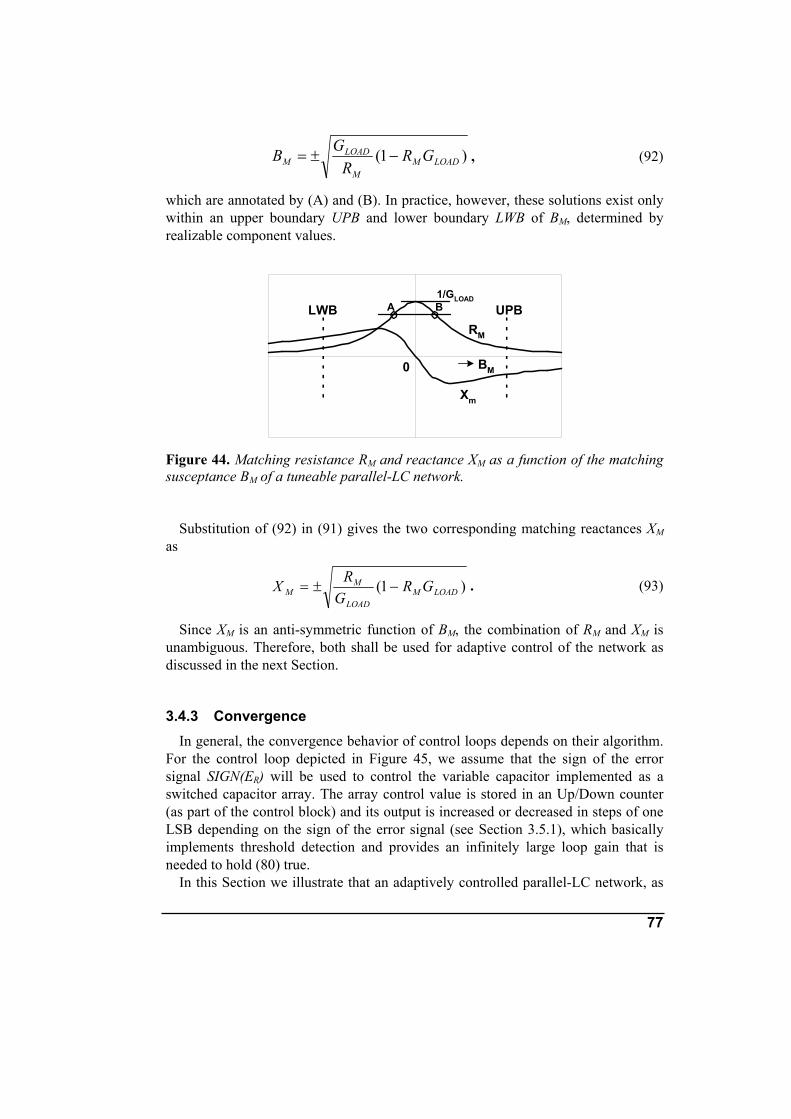
77
)1( LOADMM
LOADM GR
RGB −±= , (92)
which are annotated by (A) and (B). In practice, however, these solutions exist only within an upper boundary UPB and lower boundary LWB of BM, determined by realizable component values.
BM
Xm
RM
UPBLWB1/GLOAD
A B
0
Figure 44. Matching resistance RM and reactance XM as a function of the matching susceptance BM of a tuneable parallel-LC network.
Substitution of (92) in (91) gives the two corresponding matching reactances XM as
)1( LOADMLOAD
MM GR
GRX −±= . (93)
Since XM is an anti-symmetric function of BM, the combination of RM and XM is unambiguous. Therefore, both shall be used for adaptive control of the network as discussed in the next Section.
3.4.3 Convergence In general, the convergence behavior of control loops depends on their algorithm.
For the control loop depicted in Figure 45, we assume that the sign of the error signal SIGN(ER) will be used to control the variable capacitor implemented as a switched capacitor array. The array control value is stored in an Up/Down counter (as part of the control block) and its output is increased or decreased in steps of one LSB depending on the sign of the error signal (see Section 3.5.1), which basically implements threshold detection and provides an infinitely large loop gain that is needed to hold (80) true.
In this Section we illustrate that an adaptively controlled parallel-LC network, as

78
used for the first loop, has two solutions, causing convergence problems once embedded in a control loop. Then, we will discuss the use of a secondary feedback path to solve this problem.
Det
LSENSE
RDET ZLOADCPARLPAR
Control
ZM
ER SIGN(ER)RREF
Figure 45. Adaptive parallel-LC network controlling the real part of the matching impedance RM
The convergence behavior can easily be studied in open loop condition. When we open the loop at the controller and monitor the SIGN(ER) over the entire range of BM (representing all possible combinations of BLOAD, BC_PAR and BL_PAR), as visualized in Figure 46, then the SIGN(ER) is +1 in the two regions: BM < BM(A) and BM > BM(B). Hence, the direction of capacitor control is not unambiguous.
RM
BM
RREF
ER
0
0
SIGN(ER)
CONVERGENCE TO BDIVERGENCE
BA
Figure 46. Signal waveforms for open loop condition indicating divergence of the loop for BM < BM(A). BM is varied by tuning CPAR
As a solution to this problem, we can use detected information on the sign of the matching reactance SIGN(-XM), as a second control criterion, illustrated in Figure 47 by dotted blocks. Due to this secondary feedback path the loop control criteria are now given by the two detection thresholds RM = RREF and XM = 0 defining four quadrants of operation. Figure 48 visualizes these four quadrants I, II (shaded for clarity), III, and IV and their corresponding control criteria for BM (indicated by

79
up/down pointing double lined arrows). Assuming the detector constants KR and KD equal one, the error signal ER is now
given by
DETREFMR RRXSIGNE −⋅−= )( . (94)
Since RREF and RM are always positive, ER becomes strongly negative when the SIGN(-XM) is negative (quadrants I and IV) as illustrated in Figure 48. Hence, SIGN(ER) is now unambiguous and the loop converges reliably to operating point B over the entire range of BM.
Det
LSENSE
SIGN(-XDET)
RDET
RREF
XDET
ZLOADCPARLPAR
Control
ZM
ER
SIGN(ER)
Figure 47. Adaptive parallel-LC network controlling the matching resistance RM to RREF. The dotted blocks form an extra feedback path to enforce the first loop to operate in its stable region
BM
XM
RM=RREFA
XM=XREF=0
0
0B
RM, XM
BMIII:BMIV:
BMI:
0
CONVERGENCE TO B
ER
SIGN(ER)
RM
BMII:
Figure 48. Four quadrant control criteria (indicated by double lined arrows) of an adaptively controlled parallel-LC network. The signal waveform SIGN(ER) now indicates convergence of the loop for the entire range of BM to operating point B.

80
3.4.4 Simulations As a proof of concept, simulations on a mixed analog/digital behavioral model of
a down-converting adaptive-L network, according to the implementation in Figure 49, have been performed. The detector (see Section 3.2) of the first loop detects both the real part RDET and imaginary part XDET of the intermediate impedance ZINT for unambiguous control (see Section 3.4.3 on convergence) of RM. The sensing inductor LSERIES-B is made part of the series-LC network, which is controlled by the second loop. This loop adapts the matching reactance XM to XREF that is typically set at zero. For this loop, the generic detector provides more information than needed for proper control. In the first place, no information on the real part of the matching impedance is required, which makes RDET redundant. Secondly, at the summation point the detected reactance XDET is compared with the reference reactance XREF. Setting XREF at zero renders the summation point superfluous. And thirdly, if control of XM is done in an iterative manner, then only the sign of XDET is important. Since the magnitude of Ai is always positive, the divider function becomes redundant and the detector can be simplified even further [49].
ZM =RM+jXM
Det
LSERIES-A
Det
LSERIES-BCSERIES
XDET
XREF
SIGN(-XDET)
RDET
RREF
XDET
ZLOADCPARLPAR
U/D
EN
U/D
EN
m-bitn-bit
ZINT
EREX
1st loop2nd loop
SIGN(ER)SIGN(EX)
Figure 49. Concept implementation of an L-network. The dotted blocks form an extra feedback path to enforce the first loop to operate in its stable region.

81
3.4.4.1 Adaptive impedance matching Figure 50 shows the matching impedances ZM obtained after acquisition of both
loops for the nine different load impedances ZLOAD = 50, 100, 200 + j( -100, 0, +100). These load impedances are chosen within the tuning region of the L-network, as derived in Section 3.4.5. All matching impedance ZM are clustered around 25+0j Ω because RREF and XREF are set at 25 and 0 respectively. Deviations form ideal are caused by quantization of the capacitor values and their finite tuning range.
ZINT
ZLOAD
ZM
ZMtarget
CircleRM+jX
1st
loop
2nd
loop
Figure 50. Simulation results on a down-converting adaptive-L network. For all load impedance ZLOAD the first loop controls the match impedance on a circle segment of constant resistance RM + jX, whereas the second loop controls the reactances to approx. zero. RREF = 25, XREF = 0, and f = 900 MHz.
For three of these load conditions ZLOAD = 50 + j(-100, 0, +100) Figure 51 shows
the parallel and series capacitor values as a function of time, while both loops are adapting the capacitors from their initialization value of 5 pF toward optimum end values found. The limit cycle oscillation around these end values are caused by a 5-bit quantization of the capacitors.
To judge the effectiveness and robustness of the control algorithm we can define a relative error ER as the ratio between the magnitude of the matching reflection coefficient ΓM and that of the load ΓLOAD, normalized to 25 and 50 Ω respectively, as
50
25
LOAD
MERΓ
Γ= . (95)

82
02468
10121416
0,00 0,05 0,10 0,15-8-6-4-202468
CPA
R [p
F]
CSER
IES [pF]
t [s]
+100j
-100j0j
-100j
+100j, 0j
Figure 51. Simulated values of adaptively controlled parallel and series capacitor of an adaptive-L network. RREF = 25, XREF = 0, and f = 900 MHz.
Figure 52 shows the relative error for load impedances with a VSWR of 3, 6 and 9
over all phases. For phases between –60 and +60 degrees the relative error is approx. 0.2. Hence, the system provides about a factor 5 reduction in reflection coefficient. For mismatch phases around +/-180 degrees, minor improvement is achieved because these impedances are outside the network tuning region. It is worthwhile noting that for none of the load impedances the relative error is larger than one, which would indicate a deterioration in mismatch.
ER
0
0,2
0,4
0,6
0,8
1
-180 -120 -60 0 60 120 180
PhaseGammaLoad [degrees]
VSWRLOAD = 9 6 33
6
9
Figure 52. The relative error ER of the adaptively controlled L-network for VSWRLOAD = 3, 6, 9 over all phases. RREF = 25, XREF = 0, and f = 900 MHz.
3.4.4.2 System gain
One of the main objectives of adaptive antenna matching is to enhance the

83
maximum mobile phone output power under antenna mismatch conditions. For a 50Ω source, the gain in output power G that can be obtained by adaptive matching can be defined as the reduction in reflection loss minus the insertion loss that is introduced once we apply a tunable matching network, like
][)||1log(10)||1log(10 22 dBILG LOADM −Γ−⋅−Γ−⋅= . (96)
Figure 53 shows the simulated system gain G for load impedances with a VSWR of 3, 6, and 9 over all phases.
-3
-2
-1
0
1
2
3
4
-180 -120 -60 0 60 120 1800
1
2
3
4
5
6
7
PhaseGammaLoad [degrees]
G [d
B] VSWRLOAD = 9
6
3
36
9
IL [d
B]
Figure 53. The system gain and insertion loss of the adaptively controlled L-network for VSWRLOAD = 3, 6, 9 over all phases. RREF = 25, XREF = 0, and f = 900 MHz.
The simulated average gain is approximately 0.5, 1.5, and 2.0 dB whereas the
average network insertion loss is approximately 0.6, 1.0, and 1.3 dB respectively. Despite the low insertion loss for load mismatch phases around +/- 180 degrees, the system gain is low in this region because of the poor impedance matching of the L-network.
3.4.5 Capacitance tuning range requirement In this Section we derive relationships between the desired impedance corrections
and the required capacitance tuning ranges for the L-network depicted in Figure 49. It represents the L-network impedance tuning region.
Since the impedance transformation is done in two steps, we will first define the intermediate impedance that is required to transform an arbitrary load admittance YLOAD = GLOAD + jBLOAD to a desired matching impedance ZM= RM +jXM. For this purpose, the parallel section shall transform the load admittance to an intermediate impedance of which the real part RINT must be equal to the matching resistance RM, since the series section does not transform this intermediate resistance any further.
Using (87) and (90) and rewriting defines RINT as

84
22 )( PARLOADLOAD
LOADMINT BBG
GRR++
== . (97)
Similarly, from (91), the imaginary part of this intermediate impedance XINT can be defined as
LOADM
LOADMMINT GR
GRRX
−±=
1 , (98)
and the corresponding intermediate susceptance BINT as
LOADM
LOADMLOADINT GR
GRGB −±=
1 . (99)
The +/- signs indicate that two solutions exist. One for positive BINT (capacitive) and one for negative BINT (inductive). From (87), the required parallel capacitor CPAR is given by
2
1PARLLOADINTPAR BBB
fC −−=
π. (100)
The equations (99) and (100) define the parallel capacitance CPAR that is required to achieve a desired correction from a load GLOAD+j BLOAD to a matching resistance RM at a frequency f and a given parallel inductor susceptance BL_PAR.
Rewriting (84) gives the required value of the series capacitor CSERIES as
21
SERIESLMINTSERIES XXXf
C−+
=π
. (101)
The equations (98) and (101) give the series capacitance CSERIES that is required to achieve a desired correction from a load GLOAD+jBLOAD to a matching resistance RM and reactance XM at a frequency f and a given series inductor reactance XL_SERIES. Note, that CSERIES is independent of the load susceptance, because the parallel section compensates this susceptance. In addition, these two equations reveal that three conditions must be fulfilled.
• The square-root argument must be positive. • The parallel capacitor must be positive • The series capacitor must be positive
Therefore, firstly
LOADM G
R 1< , (102)
which represents the impedance down-converting properties of this L-network.
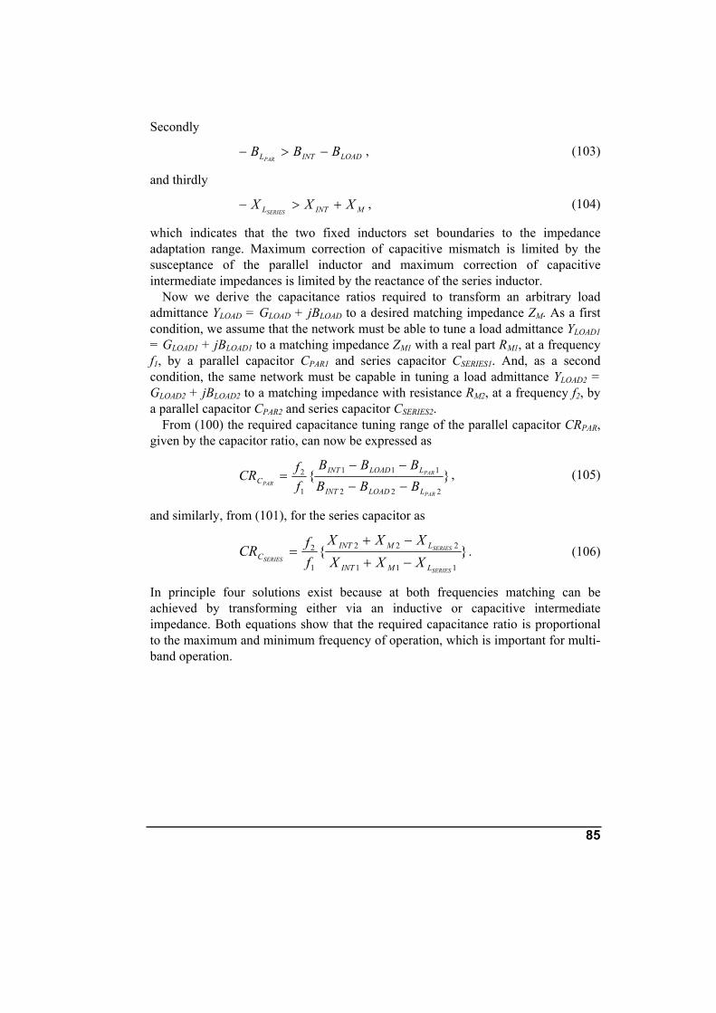
85
Secondly
LOADINTL BBBPAR
−>− , (103)
and thirdly
MINTL XXXSERIES
+>− , (104)
which indicates that the two fixed inductors set boundaries to the impedance adaptation range. Maximum correction of capacitive mismatch is limited by the susceptance of the parallel inductor and maximum correction of capacitive intermediate impedances is limited by the reactance of the series inductor.
Now we derive the capacitance ratios required to transform an arbitrary load admittance YLOAD = GLOAD + jBLOAD to a desired matching impedance ZM. As a first condition, we assume that the network must be able to tune a load admittance YLOAD1 = GLOAD1 + jBLOAD1 to a matching impedance ZM1 with a real part RM1, at a frequency f1, by a parallel capacitor CPAR1 and series capacitor CSERIES1. And, as a second condition, the same network must be capable in tuning a load admittance YLOAD2 = GLOAD2 + jBLOAD2 to a matching impedance with resistance RM2, at a frequency f2, by a parallel capacitor CPAR2 and series capacitor CSERIES2.
From (100) the required capacitance tuning range of the parallel capacitor CRPAR, given by the capacitor ratio, can now be expressed as
222
111
1
2
PAR
PAR
PARLLOADINT
LLOADINTC BBB
BBBffCR
−−
−−= , (105)
and similarly, from (101), for the series capacitor as
111
222
1
2
SERIES
SERIES
SERIESLMINT
LMINTC XXX
XXXffCR
−+
−+= . (106)
In principle four solutions exist because at both frequencies matching can be achieved by transforming either via an inductive or capacitive intermediate impedance. Both equations show that the required capacitance ratio is proportional to the maximum and minimum frequency of operation, which is important for multi-band operation.

86
3.4.6 Insertion loss The gain enhancement obtained from adaptive impedance matching is partly
undone by the insertion loss of the matching network. Therefore, these losses must be kept small. For any power matched two-port the insertion loss IL can be defined as a ratio between dissipated power and delivered output power, like
)1log(10OUT
DISS
PPIL +⋅= . (107)
For parallel elements of the L-network this power ratio equals the ratio between its loss and load conductance and for series elements the ratio between its loss and load resistance. Ignoring second-order small terms we get
)
1log(10
M
L
M
C
LOAD
L
LOAD
C
RR
RR
GG
GG
IL
SERIESSERIES
PARPAR
++
++⋅=. (108)
If we define the quality factor Q of each parallel element as the ratio between its susceptance and conductance and of each series element as the ratio between its reactance and resistance, then (108) can be rewritten as
))||||
(1
)||||
(11log(10
SERIES
SERIES
SERIES
SERIES
PAR
PAR
PAR
PAR
L
L
C
C
M
L
L
C
C
LOAD
QX
QX
R
QB
QB
GIL
++
++⋅=
. (109)
Hence, the insertion loss depends on the desired impedance transformation step as well as on the component values used to achieve that transformation. For minimum insertion loss, the susceptance of the parallel elements and the reactance of the series elements must be small, but their useful values are prescribed by the transformations to be accomplished according to (97) to (101).
Obviously, we need high element Q-factors to keep the insertion loss small, which will be illustrated in the next Section.
3.4.7 Tuning range requirement For the L-network analyzed in the previous Section, we can now calculate
capacitor values that are needed to achieve the desired impedance corrections. As a first wish, the network shall be able to match a 50 Ω load to 50 Ω illustrated as case
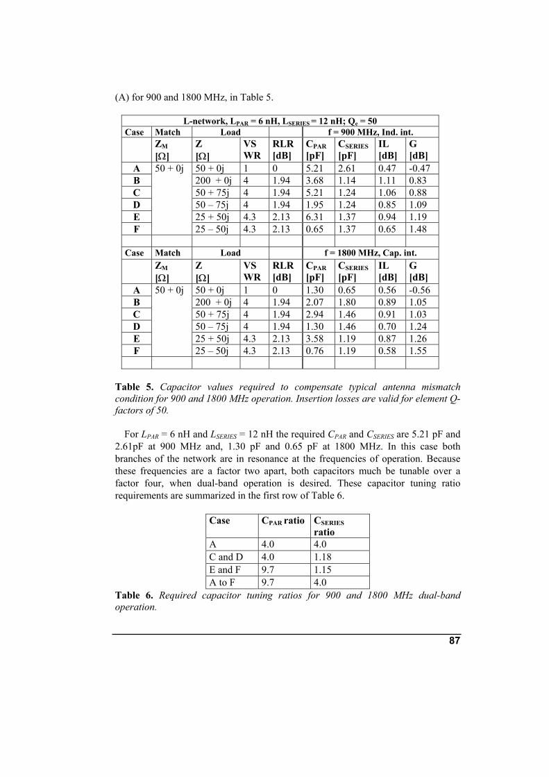
87
(A) for 900 and 1800 MHz, in Table 5.
L-network, LPAR = 6 nH, LSERIES = 12 nH; Qe = 50 Case Match Load f = 900 MHz, Ind. int. ZM
[Ω] Z
[Ω] VS WR
RLR [dB]
CPAR [pF]
CSERIES [pF]
IL [dB]
G [dB]
A 50 + 0j 1 0 5.21 2.61 0.47 -0.47 B 200 + 0j 4 1.94 3.68 1.14 1.11 0.83 C 50 + 75j 4 1.94 5.21 1.24 1.06 0.88 D 50 – 75j 4 1.94 1.95 1.24 0.85 1.09 E 25 + 50j 4.3 2.13 6.31 1.37 0.94 1.19 F
50 + 0j
25 – 50j 4.3 2.13 0.65 1.37 0.65 1.48
Case Match Load f = 1800 MHz, Cap. int. ZM
[Ω] Z
[Ω] VS WR
RLR [dB]
CPAR [pF]
CSERIES [pF]
IL [dB]
G [dB]
A 50 + 0j 1 0 1.30 0.65 0.56 -0.56 B 200 + 0j 4 1.94 2.07 1.80 0.89 1.05 C 50 + 75j 4 1.94 2.94 1.46 0.91 1.03 D 50 – 75j 4 1.94 1.30 1.46 0.70 1.24 E 25 + 50j 4.3 2.13 3.58 1.19 0.87 1.26 F
50 + 0j
25 – 50j 4.3 2.13 0.76 1.19 0.58 1.55
Table 5. Capacitor values required to compensate typical antenna mismatch condition for 900 and 1800 MHz operation. Insertion losses are valid for element Q-factors of 50.
For LPAR = 6 nH and LSERIES = 12 nH the required CPAR and CSERIES are 5.21 pF and 2.61pF at 900 MHz and, 1.30 pF and 0.65 pF at 1800 MHz. In this case both branches of the network are in resonance at the frequencies of operation. Because these frequencies are a factor two apart, both capacitors much be tunable over a factor four, when dual-band operation is desired. These capacitor tuning ratio requirements are summarized in the first row of Table 6.
Case CPAR ratio CSERIES
ratio A 4.0 4.0 C and D 4.0 1.18 E and F 9.7 1.15 A to F 9.7 4.0
Table 6. Required capacitor tuning ratios for 900 and 1800 MHz dual-band operation.

88
As a second wish, the network shall be able to compensate typical mobile phone
antenna mismatch conditions, with a VSWR of approx. 4, to 50 Ω, which are illustrated by the cases (B) to (F). In case (C) the required parallel capacitor value at 900 MHz (5.21 pF) is equal to that of case (A) because matching of 50+j75 via the inductive side is achieved by resonance of the parallel branch. A similar argument holds true in case (D) at 1800 MHz.
In the cases (B, C, and D) the load impedances are well within the range of matchable impedances of this L-network.
The cases (E) and (F), however, are chosen close to the boundary of the range of matchable impedances causing rather extreme values for the parallel capacitor. Especially in case (E) at 900 MHz the inductive load and the large inductive susceptance of LPAR have to be compensated by a large parallel capacitor (6.31 pF), while in case (F) the capacitive load is almost ideally compensated by LPAR and only little further correction is needed from the parallel capacitor (0.65 pF). To fulfill the cases (C) and (D) the series and parallel capacitor tuning range must be 4.0 and 1.18 respectively, as indicated in the second row of Table 6. Similarly, to fulfill all cases (A) to (F) their ratios shall be 9.7 and 4.0. Such capacitor tuning ratios are achievable with RF-MEMS switched capacitor arrays [63]. The inductors are typically realized as wire-wounded surface mounted devices.
In case (A) the return loss reduction is zero because impedance matching is not
improved. The insertion loss, however, is 0.47 and 0.56 dB at 900 and 1800 MHz respectively for element Q-factors of 50. Hence, the corresponding gain enhancement equals –0.47 and –0.56 dB. In the cases (B) to (F) the reduction in return loss is approximately 2 dB, but the insertion losses are increased, especially for high resistive loads and low frequencies, since the loss of the parallel inductor become very significant. Consequently, this adaptively controlled L-network effectively provides an gain enhancement of approximately 1 dB over the indicated impedance range.
3.4.8 Conclusions on adaptively controlled L-network
• An adaptive impedance matching technique for controlling L-networks is presented.
• It uses a cascade of two loops for independent control of the real and imaginary part of the matching impedance.
• For unambiguous control of the real part of the impedance, a secondary feedback path is used to enforce operation in to a stable region, when needed.
• The basic properties of tunable series and parallel LC-networks have been treated upon which these adaptation techniques are based.

89
• In combination with the true-orthogonal impedance detector applied, robust control is achieved by a simple algorithm that can either be implemented in software or by basic mixed analog/digital circuits.
• Relationships between desired impedance correction and required capacitance tuning ranges are derived. For the indicated impedance adaptation region, the required capacitor tuning ranges are realizable with RF-MEMS switched capacitor arrays.
• For load impedances with a VSWR of 3, 6, and 9, the simulated system gain, averaged over all phases, is typically 0.5, 1.5, and 2.0 dB respectively.
In more detail, network analysis reveals that:
• Due to the network topology, a down-converting L-network can convert the impedance of a resistive load only to a lower resistance, which limits the impedance tuning region of the network topology.
• In general, the non-linear transfer characteristic of an L-network has two solutions that provide the desired impedance transformation.
• These two solutions can be discriminated by the sign of the intermediate susceptance sign(BINT), which requires detection at the intermediate node.
• Information on the sign of the intermediate susceptance is used as a control criterion for a secondary feedback path, providing unambiguous control of RM.
• Adjustment of the matching resistance RM causes a change in the matching reactance XM, however.
• The imaginary part of the matching reactance XM can be adjusted by changing the reactance of the series branch, without affecting RM.
• Hence, robust orthogonal control of a down-converting L-network is possible.
• Thanks to the principle of duality, an up-converting L-network has similar properties that can similarly be described by changing impedance into admittance and vice versa.
Furthermore, network analysis on a parallel-LC network reveals that:
• A variable parallel-LC network is well suited for adaptation of the matching susceptance BM without affecting the matching conductance GM because:
o The matching susceptance BM is a monotone function of the total susceptance BTOT of matching network and its load admittance, and
o The matching conductance GM is fully independent of the total susceptance BTOT.
• A parallel-LC network is very useful in controlling the matching

90
resistance RM because: o RM is a symmetric monotone function of the total susceptance
BTOT of which o The two solutions, that might exist, can be distinguished by the
sign of the matching reactance XM. • Its matching resistance RM depends on the total susceptance BTOT,
however. • The maximum achievable matching resistance RM is limited to 1/GLOAD. • Thanks to the principle of duality, a Series-LC network has similar
properties that can similarly be described by changing impedance into admittance and vice versa.

91
3.5 Adaptive series-LC matching network using RF-MEMS In this Section, an adaptively controlled series-LC matching network is discussed
[49] that compensates the imaginary part of the antenna impedance. We will exploit the capabilities of capacitive RF-MEMS switches among which their large tuning range. As a bottom-up approach, we discuss the design of an RF-MEMS unit cell that is used for the realization of a variable capacitor implemented as a 5-bit binary weighted array. It is fabricated in a RF-MEMS technology [64], [65] that is optimized for multi-standard mobile phone applications. Communication protocol specific requirements on minimum RF-MEMS pull-in and pull-out voltage are derived, which dictates the actuation voltages needed. These actuation voltages are generated by a high-voltage driver IC providing a bipolar biasing wave-form with a low 60/30 V actuation/hold duty-cycle in order to minimize dielectric charging and thus to improve MEMS reliability. A wafer-to-wafer bonding method is applied to obtain a sufficiently hermetic package [48].
Currently, alternative technologies are under development striving to meet the very demanding requirements on linearity, insertion loss, and tuning range that are imposed by cellular phone applications.
Research on Barium-Strontium-Titanate (BST) [41] and silicon varactors [42] have resulted in continuously tunable, linear, and low loss devices. However, their effective tuning range, limited by forward biasing and breakdown under large signal conditions, is only a factor of 3. A slightly larger effective tuning range and high linearity is obtained from CMOS switches on sapphire [43], [44] and SOI [45], but their RON·COFF product is still large compared to that of capacitive RF-MEMS switches. CMOS switches are controlled by low voltages (3 V) and, in principle, the technology can be used to implement mismatch detectors and control logic, which can result in a high level of integration. RF-MEMS capacitive switches are well known for their exceptionally large tuning range, high linearity, and very low loss [46], [47], but they still suffer from dielectric charging and mechanical deformation.
3.5.1 Adaptive tuning system In mobile phones, often a planar inverted-F antenna (PIFA) is used that behaves
as a series resonance circuit at low-band (LB ~ 900 MHz) as well as at high-band (HB ~ 1800 MHz). Body-effects cause mainly a down shift in resonance frequency resulting in a more inductive impedance at the antenna feed point. In this case study, we have chosen for correction of antenna mismatch by a tunable series-LC matching network because it is the simplest network that effectively compensates the inductive antenna behavior when this matching network is placed close to the antenna feed point. A fundamental restriction of this one-dimensional matching network is that any change in the real part of the antenna impedance cannot be compensated. A block diagram of the adaptively controlled series-LC matching

92
network is depicted in Figure 54. It comprises a tunable 5-bit switched capacitor array, high-voltage MEMS biasing switches, a high-voltage generator, a phase detector, and an up/down counter.
Figure 54. Block diagram of an adaptive series-LC matching network. It compensates the reactive part of the load impedance by controlling the detected phase φZ_DET of the matching impedance to zero.
Mismatch information is given by the phase of the matching impedance ZM at the network input. It is determined by the phase difference between the network input voltage u and its input current i. The voltage u is measured single-ended, whereas a measure of the branch current i is obtained from the differential voltage across the sensing inductor LSERIES. The detected phase φZ_DET is obtained from a mixer that is driven by hard limited input signals and is given by [66], [67],
)(2iuZDET
ϕϕπ
ϕ −= . (110)
The phase detector output signal φZ_DET is fed to a limiter to determine the sign of the phase. Depending on this sign the counter will either increase or decrease its output value in steps of 1-LSB (least significant bit). The counter outputs control the high-voltage switches to bias the RF-MEMS devices of the switched capacitor array. Updates of the array are made under control of a base-band enable signal EN that can be synchronized to the frame repetition rate of the GSM/EDGE/W-CDMA transmission protocols. Consequently, the loop controls the phase of the detected

93
impedance φZ_DET to zero step by step, keeping phase transients of the transmitted signal small.
In this concept, the series inductor LSERIES has three functions. Firstly, it provides impedance transformation as part of the matching network. Secondly, it acts as an sensing element from which information on mismatch is obtained. And thirdly, it provides +90 degrees phase shift required for proper phase detection. The photograph in Figure 55 shows the adaptive antenna matching module that consists of a Si-capped RF-MEMS die, a detector die, and a high voltage generator die, all wire bonded to laminate. The module contains two SMD components: a 1 nF high voltage buffer capacitor and an inductor for ESD protection at the antenna terminal.
Figure 55. Photograph of the adaptive antenna matching module showing the packaged RF-MEMS, high-voltage generator, and impedance phase detector dice. 3.5.1.1 Series-LC matching network
The impedance matching properties of a series-LC matching network have already been formulated, as part of the L-network, in Section 3.4.2.1. For the sake of completeness, we state again that the matching impedance ZM at the input of a series-LC network, as shown in Figure 56, is defined as
MMM jXRZ += , (111)
in which the matching resistance RM is given by
LOADM RR = , (112)
and the matching reactance XM by
LOADCLM XXXXSERIESSERIES
++= . (113)

94
Tuning the series capacitor value CSERIES changes the matching reactance XM over a circle segment of constant resistance RLOAD as visualized in the Smith chart in bold. It is a monotone function of the tunable reactance XC_SERIES. The matching resistance RM is equal to the load resistance RLOAD and fully independent of the tunable reactance XC_SERIES. Hence, the proposed concept cannot compensate for fluctuations in the real part of the antenna impedance.
Figure 56. A tuneable series-LC network providing correction for inductive and capacitive load reactance visualized on a Smith chart.
3.5.1.2 Capacitance tuning range
In this Section we derive the capacitance ratio required to transform an arbitrary load reactance XLOAD to a desired matching reactance XM. As a first condition, we assume that the network must be able to tune a load reactance XLOAD1 to a matching reactance XM1, at a minimum frequency f1. As a second condition, the same network must be capable in tuning a load reactance XLOAD2 to a matching reactance XM2, at a maximum frequency f2. Rewriting (113) gives the series capacitor CSERIES as
)1(21
SERIESLMLOADSERIES XXXf
C+−
=π
. (114)
From (114), the required capacitance ratio of the tunable series capacitor CRC_SERIES can now be expressed as
1
2
11
22
1
2
SERIES
SERIES
SERIESLMLOAD
LMLOADC XXX
XXXffCR
+−
+−= . (115)
This equation reveals two important network properties. Firstly, the required ratio becomes excessive when the denominator approaches zero, which occurs when the desired correction in capacitive reactance |XLOAD1-XM1| equals the reactance of the series inductor |XL_SERIES1|. Hence, this tunable network is not very capable in

95
correcting capacitive mismatches (but well capable in correcting inductive mismatches). Secondly, the required capacitance ratio is proportional to the ratio between the required maximum and minimum frequency of operation, which is important for multi-band applications. We have chosen for this tunable series-LC network because its tuning range fits to the typical behavior of PIFAs [68] that become inductive under the influence of body-effects (see measurement results in paragraph 3.5.3.4). In addition, we exploit the large tuning range of RF-MEMS capacitive switches to meet tuning range requirements. 3.5.1.3 Simulations
The functionality of the adaptive series-LC matching network has been verified by ADS ENVELOPE [62] simulations using behavioral models. Acquisition of the adaptive loop is simulated for the load impedances (30, 50, 70) +j(-25, 0, +25, +50, +75) Ω, that are marked by solid dots in Figure 57. The lines over circle segments of constant resistance show the trajectories of impedance adaptation as a function of time. Once the steady state condition is reached the matching impedances, designated by open squares, are clustered around three points close to the real axis of the Smith chart.
Figure 58 shows the corresponding series capacitor values, as a function of time (nr. of iterations), for the load impedances 50 + j(-25, 0, +25, +75) Ω. The capacitor value is initialised at 6 pF and adapts, in steps of 0.5 pF, to a minimum value of 1 pF for an inductive load of +75j and to 10 pF for a capacitive load of –25j.
Obviously, a large inductive mismatch as well as a small capacitive mismatch (that correspond to expected PIFA feed point impedances) are well compensated by this series-LC network, requiring a capacitance tuning ratio of 10. Once, after approximately 10 iterations, acquisition of the loop is obtained, a limit cycle oscillation of +/-1-LSB is visible that is caused by quantization of the capacitor value.

96
Figure 57. Simulated impedance mismatch adaptation. The load impedances 30, 50, 70 + j(-25, 0, +25, +50, +75) Ω are adapted to approx. 30, 50, and 70 Ω over circle segments of constant resistance. f = 900 MHz.
Figure 58. Series capacitor value as a function of time (nr. of iterations) for the load impedances 50 + j(-25, 0, +25, +75) Ω. f = 900 MHz.

97
3.5.2 Adaptive RF-MEMS system design As a bottom-up approach, we will now treat the design of an RF-MEMS unit cell,
a 5-bit RF-MEMS array constructed out of such unit cells, and the high-voltage generator. In addition, application specific requirements on RF-MEMS pull-in and pull-out voltages are derived that determine the minimum voltage needed for actuation.
3.5.2.1 RF-MEMS unit cell design
In theory [46], the capacitance of a MEMS device CMEMS as a function of the gap height g, depicted in Figure 59, is given by
r
dr
MEMS ttg
AC
ε
ε
++= 0 , (116)
in which ε0 is the free space dielectric constant, A is the effective MEMS capacitance area, tr is the effective surface roughness of the beam and dielectric layer, modeled as an equivalent residual air gap, and td and εr are the thickness and relative dielectric constant of the dielectric layer. The MEMS capacitance ratio CRMEMS between the ON and OFF capacitance of the MEMS device, given by the condition g = 0 and g = g0 respectively, can now be written as
r
dr
MEMS tt
gCR
ε+
+= 01 . (117)
Table I summarizes representative process and design parameter values and corresponding unit cell properties. Although roughness tends to halve the effective ON capacitance an impressive tuning range of 16 is achieved for the intrinsic part of the device. In practice, however, bending of the top plate and parasitic capacitance of the springs will affect the ON and OFF capacitances, causing a reduction in tuning ratio. It is worthwhile noting that the adaptively controlled series-LC network is not sensitive to spreads in these parameters because it automatically compensates for deviations in capacitance value.

98
Figure 59. RF-MEMS capacitive switch model including effective surface roughness.
Process and design
parameters Unit cell properties
(Section III-A) g0 3 µm CON 4.4 pF tr 0.1 µm COFF 0.275 pF td 0.5 µm CRMEMS 16 εr 5 UPI 45 V ε0 8.85e-12 F/m UPO 6.6 V A 200x500 µmk 200 N/m
Array properties (Section III-B)
r 3 CP 1 pF CARRAY_MIN 2 pF CARRAY_MAX 16 pF CRARRAY 8
Table 7. Representative RF-MEMS process and design parameter values, corresponding unit cell, and array properties. Figure 60 depicts a lay-out of the unit cell with a ground-signal-ground (GSG) connection for RF characterization. It consists of a rectangular top plate that is supported by four springs sharing two anchors as fixed points. A 3x9 pattern of holes at a pitch of 50 µm is used in the top plate for reduced squeeze film damping [69], which reduces the switching time9 to approximately 100 µs. A representative CV-curve of the unit cell is shown in Figure 61. The bi-stable device goes in ON-
9 The holes in the moving top plate act as gas inlets and outlets, which strongly affects the gas flow in the narrow gap between the fixed and moving plate and thus the dynamics of the moving plate.

99
state when the actuation voltage UACT exceeds the pull-in voltage UPI and switches back to the OFF-state when UACT becomes smaller than the pull-out voltage UPO.
Figure 60. Lay-out of a 4 pF RF-MEMS unit cell in an on-wafer ground-signal-ground RF characterization structure
Figure 61. Typical CV-curve of a RF-MEMS capacitive switch as used as unit cell in the 5-bit array.

100
3.5.2.2 RF-MEMS switched capacitor array design The unit cell is used as building block for the realization of a 5-bit binary
weighted switched capacitor array, conceptually depicted in Figure 62. Each bit is activated via a bias control line b. In series with the RF-MEMS DC-blocking capacitors CDC are required to isolate the biasing lines from each other for individual actuation. The resistors R provide RF-isolation between the RF-paths and the DC biasing lines and have high impedances to minimize insertion loss.
Figure 62. Binary weighted RF-MEMS switched capacitor array, including DC-block capacitors and bias resistors, and its corresponding control curve.
The minimum array capacitance CARRAY_MIN is given by the sum of all RF-MEMS devices in OFF-state plus a parasitic capacitance CP in parallel to the array
PnOFFMEMSMINARRAY CCC += ∑ ___ . (118)
Similarly, the maximum array capacitance CARRAY_MAX is given by the sum of all RF-MEMS devices in ON-state plus the same parasitic capacitance CP
PnONMEMSMAXARRAY CCr
rC ++
= ∑ ___ 1. (119)
The factor r/(r+1) stems from the DC-blocking capacitors that reduce the effective maximum capacitance of the array when the DC-blocking capacitance is made r times larger than the ON capacitance of the corresponding RF-MEMS device. The capacitance ratio of the array CRARRAY can now be written as
∑
∑+
++=
PnOFFMEMS
PnONMEMS
ARRAY CC
CCr
r
CR__
__1 . (120)
If the parasitic capacitance CP can be neglected with respect to the sum of ON-capacitances, expressed by the numerator, the array capacitance ratio can be

101
simplified in to
∑++
=
nOFFMEMS
PMEMSARRAY
CCCR
rrCR
__
1
11
, (121)
in which CRMEMS is the MEMS ON/OFF capacitance ratio. Preferably, the parasitic capacitance is kept small with respect to the sum of MEMS OFF capacitances.
Initially, the array was designed for a wide tuning range from approximately 1 pF to 15 pF with small steps of 0.5 pF to minimize the impedance step size. To achieve a reasonable compromise between control curve accuracy, required chip area, and capacitance ratio of the array two major design choices have been made. Firstly, the programmable capacitors are constructed out of parallel and series combinations of unit cells to secures monotonicity in the capacitor control curve and good matching of the pull-in and pull-out voltage over the wide range of capacitor values. Secondly, the unit cells are DC isolated from each other by MIM capacitors that are all similarly scaled by a capacitance ratio r of 3. Throughout the design process a parasitic capacitance CP of almost 1 pF turned out to be present, which tends to halve the array tuning range. The array is implemented in an 5 kΩ·cm high-resistive passive silicon technology [49]. Wafer-to-wafer bonding is applied to provide hermetic enclosure of the MEMS devices [48]. A die photograph of the array is depicted in Figure 63.
Figure 63. Die photograph of a 5-bit switched capacitor array using 4 pF RF-MEMS unit cells with integrated DC-block MIM capacitors and bias resistors.

102
3.5.2.3 Pull-in and pull-out voltage requirements In this Section we derive minimum requirements for pull-in and pull-out voltage
of the RF-MEMS unit cell. The pull-in voltage must be chosen sufficiently large in order to avoid self-actuation of the RF-MEMS due to RF. The pull-out voltage must be sufficiently large to avoid non-release of the RF-MEMS under hot-switching conditions. Self-actuation and non-release occur when the RMS (root-mean-square) voltage across the capacitor exceeds the pull-in voltage or pull-out voltage respectively. Potentially, it prohibits adaptive impedance correction at high output power while a strong inductive mismatch is present, thus when adaptation is needed most. The RMS voltage across the variable series capacitor UC_SERIES is given by
LOAD
LOADSERIESCSERIESC R
PXU ⋅= __ , (122)
in which PLOAD is the power delivered to the load resistance RLOAD and XC_SERIES is the reactance of the variable series capacitor. Two operating conditions have been identified that dictate the required pull-in and pull-out voltage
Firstly, the largest RMS voltage can be expected for low-band operation in GSM-mode, while all RF-MEMS devices are in OFF-state, because for this condition the maximum specified power PLOAD and the reactance XC_SERIES are largest. For PLOAD = 3.2 W, RLOAD = 50 Ω, CSERIES = 1 pF, and f = 900 MHz, UC_SERIES equals 45 V, according to (122). Hence, to avoid self-actuation the pull-in voltage must be at least 45 V.
Secondly, non-release of the beam occurs most likely for low-band operation in W-CDMA-mode, while only the LSB is in ON-state, because in W-CDMA-mode hot-releasing of the RF-MEMS devices is needed (the protocol does not provide idle slots in which cold-switching could be done) and the reactance to be released is largest. For PLOAD = 0.63 W (maximum peak power), RLOAD = 50 Ω, CSERIES = 1.5 pF, and f = 900 MHz, UC_SERIES equals 13.2 V. To avoid non-release the pull-out voltage shall be at least 13.2 V, according to (122). This latter requirement is only relevant for the least significant bit, because when other bits are ON the voltage across the array remains significantly lower. Hence, we can reduce this pull-out voltage requirement to 13.2/2 = 6.6 V by implementing the LSB by two RF-MEMS unit cells in series.
Because of these application specific requirements a high-voltage driver IC [70] is needed to bias the RF-MEMS devices, which will be discussed in paragraph 3.5.2.4.
3.5.2.4 High voltage driver IC
In order to actuate RF-MEMS devices with a 45 V pull-in voltage, as derived in paragraph 3.5.2.3, a biasing voltage in excess of the pull-in voltage is needed. A major disadvantage of such a high actuation voltage is an enhanced charging of the MEMS dielectric layer, which causes a down shift of the RF-MEMS pull-in and pull-out voltage that might result in self-actuation and non-release.

103
To combat shifts in CV-curves we apply a biasing schema with a minimum average actuation voltage that is accomplished by two measures: (1) a 60/30 V actuation voltage with small duty-cycle, and (2) a bipolar waveform to alternate the polarity of charging. A simplified (single-ended) biasing wave-form is depicted in Figure 64. During a relatively short interval, determined by the switching time of the RF-MEMS devices (typically 100 ms), a 60 V actuation voltage UACT is applied. Then, the actuation voltage of all MEMS devices in ON-state goes down to a hold voltage UHOLD of 30 V. This hold period lasts for a relatively long time (typically 10 to 100ms), because a slow rate of impedance adaptation can be chosen to follow the even slower fluctuations in hand-effects. The polarity of actuation is changed at a typical rate of 1 Hz because the major dielectric charging mechanisms found are even slower.
Figure 64. Typical high-voltage generator output voltage waveform that provides reduced dielectric charging of RF-MEMS capacitive switches.
Figure 65 shows a block diagram of the driver IC. It consists of a charge pump,
high-voltage output switches, and two output voltage control loops. The charge-pump, switched at 20 MHz, gradually charges a 1 nF SMD (surface mounted device) buffer capacitor under control of the 60 V stabilization loop. The 30 V control loop provides down-ramping and voltage stabilization of an internal node, which minimizes power losses of the charge-pump. The 60/30 V wave-form supplies the high voltage output switches that are in parallel to separately bias each bit of the MEMS array. This high voltage generator is implemented in a 120 V SOI process offering good isolation.

104
Figure 65. Block diagram of the high-voltage generator providing a 60 V “actuation” and 30 V “hold” voltage. The bridge circuit allows for bipolar actuation of the RF-MEMS devices.
3.5.2.5 Module insertion loss Power dissipation in the matching network must be kept small because it
diminishes the effective transmitter efficiency enhancement obtained by improved impedance matching. For any power matched two-port the insertion loss IL can be defined as a ratio between dissipated power PDISS and power delivered to the load PLOAD, like
)1log(10LOAD
DISS
PPIL +⋅= . (123)
The ratio between dissipated power and load power equals the ratio RSERIES / RLOAD for a series loss resistance and the ratio RLOAD / RPAR for a parallel loss resistance respectively. Hence, for a 50 Ω load impedance, and ignoring second-order small terms, the insertion loss of the lumped equivalent series-LC network, shown in Figure 66, can be expressed as
)21log(10SUB
LOAD
BIAS
LOAD
LOAD
DC
LOAD
MEMS
LOAD
CROSS
LOAD
L
RR
RR
RR
RR
RR
RR
IL SERIES ++++++⋅= , (124)
in which RL_SERIES, RCROSS, RMEMS, RDC, RBIAS, and RSUB are the equivalent loss resistances of the series inductor, bond frame crossing, RF-MEMS capacitors, DC-block capacitors, MEMS bias resistors, and that of the high-resistive silicon substrate respectively. Estimates of these lumped equivalent loss resistances, given in Table 8, have been obtained from simulations with SONNET [71]. Their values

105
clearly illustrate that network losses are dominated by the loss resistance of the series inductor (implemented in laminate), the equivalent parallel MEMS biasing resistors, and the two bond frame crossings. These crossings introduce a significant amount of loss because their widths has been made small in order to minimize parasitic capacitance between the RF-path and the bond frame.
Figure 66. Lumped equivalent circuit representing losses of the series-LC network.
Equivalent loss resistance IL
[Ω] [dB] RL_SERIES 1.3 0.11 2·RCROSS 0.6 0.05 RMEMS 0.2 0.02 RDC 0.2 0.02 RBIAS 2k 0.11 RSUB 5k 0.04 Total IL 0.35
Table 8. Equivalent loss resistances and their contributions to the insertion loss of the module.
3.5.3 Experimental verification In this Section we present, again as a bottom-up approach, experimental results on
the MEMS switched capacitor array, followed by results on the entire module in open loop, and finally results on an adaptively controlling module connected to a planar inverted-F antenna (PIFA). For each specification evaluation is done for the most demanding cellular phone mode of operation.
3.5.3.1 RF-MEMS switched capacitor array
The RF-MEMS array capacitance as a function of frequency is evaluated by on-wafer measurements and the results are compared to SONNET [71] EM-simulation in Figure 67a. The capacitance in OFF-state (00000) is approximately 2 pF for

106
measurements and simulations, which is a factor two more than the initial design target. For MSB ON-state (10000) the measured capacitance of 10 pF is only 20 % larger than the simulated value of 8 pF, which might be caused by a difference in surface roughness. This results in a capacitance tuning ratio of almost 10.
Series resonance occurs due to a parasitic equivalent series inductance (ESL) of approximately 1.6 nH. Fortunately, for this module the ESL is harmless because it can easily be embedded in the desired series inductance.
For the various capacitance values, measurements and simulations show an insertion loss in the range of 0.3 to 0.6 dB at 1 to 2 GHz, as depicted in Figure 67b. At lower frequencies the insertion loss increases drastically due to parasitic substrate shunt resistance, whereas at higher frequencies series resistance and skin effects of interconnect lines cause an increase in insertion loss.
State00000
10000
00100
10000 00100
State00000
-1*
Figure 67. Simulated and measured capacitance (a) and insertion loss (b) of the 5-bit switched capacitor array for three different capacitor values.

107
3.5.3.2 Module insertion loss Under 50 Ω and open loop conditions, the insertion loss of the entire module is
measured at approximately 0.5 dB for low-band and high-band, as shown in Figure 68. These losses are predominantly caused by the series inductor and switched capacitor array biasing resistors, as discussed in paragraph 3.5.2.5. The notch at 1.2 GHz results from a dual-banding network (see Appendix B on dual-banding networks).
-3,0
-2,0
-1,0
0,0
5,0E+08 1,0E+09 1,5E+09 2,0E+09 2,5E+09
LB HB-1
*IL [d
B]
f [Hz] Figure 68. Module insertion loss as a function of frequency.
3.5.3.3 Module distortion
For a 50 Ω load and f = 900 MHz, the second- and third-order harmonic distortion of the module is measured as a function of power delivered to the load. These harmonic components, shown in Figure 69, remain below –85 dBc up to 35 dBm output power, which is more than sufficient to meet the system specification of –83 dBc.
Figure 69. Measured 2nd- and 3rd-order harmonic distortion as a function of input power.
In a multi-standard environment the reception of weak signals is hampered by

108
strong interferers causing in-band inter-modulation products. Therefore, RF front-end inter-modulation distortion requirements are very demanding [28] and usually difficult to meet. We verified third-order inter-modulation distortion (IM3) for a +20 dBm wanted W-CDMA signal at 1.96 MHz and a –15 dBm interfering GSM signal at 1.76 MHz, causing an unwanted frequency component in the W-CDMA receive band at 2.16 GHz. The IM3 component is measured at –117 dBm and is caused by the measurement set-up rather then by the module itself. It remains well below the specified –105 dBm. Hence, linearity specifications for operation in a multi-standard environment are well met.
Distortion due to modulation is verified in EDGE-mode, because MEMS devices are most susceptible to amplitude modulation when a relatively large part of the power distribution falls within their mechanical bandwidth [73]. Up to 27 dBm output power, distortion due to EDGE modulation turns out to remain below the measurement set-up distortion level of approximately 1 % for EVM and –70 dBc for ACPR. Both are well below typical RF front-end specifications of 2.5 % and –60 dBc for EVM and ACPR respectively.
3.5.3.4 Adaptive module connected to an antenna
Measurements are performed on the complete module connected to a planar inverted-F antenna (PIFA). First, the module input impedance is measured for an open loop condition in which the MEMS-array setting is fixed. A hand is moved towards the PIFA, touching its enclosure, and then covering it completely. During this action, the impedance moves away from the center of the Smith chart, as depicted in Figure 70 by black triangular markers. Next, the action is repeated, while the adaptive loop is closed. For all hand positions the module input impedance now remains close to the center, as illustrated by the gray solid dots. For extreme hand-effects the maximum module impedance correction is -75j Ω. Hence, the module corrects antenna impedance disturbances as expected.

109
Figure 70. Input impedance of the adaptive module when connected to a PIFA that is influenced by hand-effects, for open loop and closed loop conditions. f = 900 MHz.
3.5.4 Conclusions on adaptive series-LC matching module
• A multi-standard adaptively controlled series-LC matching network is presented, which is implemented with RF-MEMS capacitive switches.
• Following a bottom-up approach, the design of a RF-MEMS unit cell for the construction of a 5-bit switched capacitor array has been described.
• Application specific requirements on RF-MEMS have been derived, in particular on pull-in and pull-out voltage, emphasising the need for a high actuation voltage. For this purpose, a high voltage driver IC is developed that reduces dielectric charging of the MEMS devices, by generating a bipolar waveform with low high/low duty-cycle to minimize the average actuation voltage.
• The module insertion loss is measured at 0.5 dB for low-band and high-band.
• Measurements prove that all system requirements on distortion are well met for GSM, EDGE, and W-CDMA mode of operation.
• Adaptive correction of the reactance of a planar inverted-F antenna is demonstrated. For extreme hand-effects the maximum module impedance correction is -75j Ω, at 900 MHz.
• The results accomplished prove the feasibility of RF-MEMS based adaptive antenna matching modules, for application in multi-standard mobile phones.

110
3.6 Load line adaptation
3.6.1 Introduction In this Section a load line adaptation concept is presented that makes use of an
impedance-inverting matching network, which provides power amplifier efficiency enhancement over an unusually large range. Although power efficiency enhancement methods are not subject of this thesis, this Section is devoted to load line adaptation because it makes use of circuit techniques and requires enabling technologies, which are very similar to those for adaptive impedance control techniques, presented in the previous Sections of this Chapter.
Usually, class-AB power amplifiers suffer from low power efficiency at medium
output power, because their load line is typically optimized for maximum output power. In principle, adaptation of the load line as a function of output power can be applied to improve PA efficiency at medium power levels [75], [76]. In this Section some novel ideas on power amplifier load line adaptation are presented.
In Section 3.4.5 to 3.4.7 basic design equations on variable down-converting L-
networks have been derived, defining the limitations on impedance tuning range, maximum-to-minimum component values and insertion loss. It was shown that, according to theory and simulations, a single L-network gives excessive insertion loss for large impedance transformation ratios. Moreover, network analysis revealed that the implementation of a variable inductance as a combination of a fixed inductor and variable capacitor makes insertion loss even worse. This is very undesirable, because it would result in a huge PA efficiency degradation at high output power, for which a large impedance transformation ratio is typically required.
As a solution to this problem, it is proposed to use a fixed matching network
between the power transistor and the adaptive matching network that acts as an impedance inverter. The use of such an impedance inverter results in a relatively low insertion loss at high power, but in larger losses at medium power, because at medium power the variable network needs to provide a larger impedance transformation. The latter limits the effectiveness of load line adaptation at medium power levels. In addition, the usage of a fixed matching network allows for the implementation of transmission zeros (to reject harmonics) and to provide a well defined collector load impedance at the second harmonic (for instance, for class-E or class-F operation), independent of the (variable) load impedance at the fundamental frequency.

111
3.6.2 Concept In Figure 71 the new adaptive load line matching concept is shown. First, an
adaptive matching network transforms the load resistance RLOAD to a matching resistance RM. Then, the fixed impedance-inverting network (with a characteristic impedance of Z0) transforms RM to a load line resistance RLL. Optimum efficiency is now obtained by setting RM as a function of output power according to
220 )(
2
SATSUPPLY
LOADM UU
PZR−
⋅⋅= . (125)
Thus, a priori knowledge on the required output power PLOAD, supply voltage USUPPLY, collector saturation voltage USAT, and characteristic impedance Z0 can now be used to set the matching resistance RM. The imaginary part of ZM shall remain zero, while the impedance-inverting network preserves this reactance of zero over the entire impedance transformation range.
R
Fixedmatchingnetwork
Rref
Adaptivematchingnetwork
Rload
32
32
2
2
LOG(RLL)
LOG(RM)
llmo RRZ ⋅=
Zm=RmZll=Rll
Z0 = 8
Figure 71. Load line adaptation concept using a fixed impedance-inverting network in between the power transistor and adaptive matching network.
In principle a load line adaptation concept can be implemented as:
• Feed forward controlled • Adaptively controlled, by either a
o 1-step algorithm o Iterative algorithm

112
A feed forward controlled system does not make use of an impedance detector and
detailed a priori knowledge of the variable network is required for proper control. For optimum performance constant (antenna) load impedance is a prerequisite. The matching network is controlled by base-band that uses a look-up table with extended calibration data of the variable matching network.
In case of adaptive control, a mismatch detector provides information on the matching impedance, which is used for adjustments of the matching network in accordance to output power levels. Within the range of adaptation this concept can cope with mismatches of the load, which is an advantage of adaptive control over a feed forward controlled system.
A 1-step algorithm makes use of a look-table with S-parameter data of each setting of the matching network obtained from calibration or a reference design. The detected impedance and S-parameter data of the current setting are used to calculate the actual antenna load impedance ZLOAD. From this calculated ZLOAD and the required output power level a new optimum setting is calculated. Then, at a proper moment (in an idle slot, or during a slot boundary) the network setting is updated. The usage of detailed a priori knowledge on the impedance transformation properties of the network makes this algorithm fast.
In case of an iterative adaptation algorithm less a priori knowledge on the variable matching network is required. Often, monotone control is a sufficient requirement to guarantee proper convergence as discussed in Section 3.1.3. Information of detected mismatch is used to slightly adjust the network in the proper direction until, step-by-step, an optimum match is achieved. Such iterative algorithms are slow and therefore unsuited to follow rapidly changing slot-to-slot output power variations that happen in GSM/EDGE as well as in UMTS.
Table 1 gives an overview of the basic properties of the discussed load line control methods.
Concept Pros Cons Feed forward controlled
Fast No detector required
Calibration needed Load dependent
1-step adaptive Fast Load independent
Calibration needed Detector required
Iterative adaptive Load independent No calibration
Very slow Detector required
Table 9. Advantages and disadvantages of feed forward and adaptively controlled load line.

113
3.6.3 Implementation of load line adaptation A circuit block diagram of the proposed feed forward controlled output matching
network is depicted in Figure 72. An L-network with variable parallel and series capacitors converts the load impedance RLOAD according to (125) down. Both variable capacitors consist of a binary weighted array of (RF-MEMS) switched capacitors. Their settings are determined by a digital code stored in a register.
The fixed matching network consists of two L-networks that act as an impedance inverter with a characteristic impedance Z0 of 8 Ω. The series resonant circuits in each parallel branch reject frequency components at the second and third harmonic. DC-supply is applied at the center node of this matching network because its impedance remains relatively low (approximately 8 Ω) over the entire range of impedance adaptation. This feed is made parallel resonant to achieve sufficient isolation to the supply for a relatively small size inductor.
Rload
Register
Level shifter
Lseries
5
CseriesC
2C
4C
8C
16C
CparC2C4C8C16C
5
2f0 3f0
Figure 72. Power amplifier with fixed impedance-inverting matching network and a feed forward controlled variable matching network.
A 3-wire bus (I2C) can be used to interface with a base-band controller to set the register. The register outputs control the high voltage switches that supply 30 to 60 V to the RF-MEMS device for electrostatic actuation.
An example of an adaptively controlled load line, based on a 1-step algorithm, is shown in Figure 73. It contains a variable L-network and fixed impedance-inverting network, which are similar to that of the feed forward controlled concept. In addition, however, an impedance detector is placed in between these two networks to measure the matching impedance. LSERIES is used as sensing element of the detector. The detector outputs RDET and XDET are passed over to the base-band controller to determine a new value to be down loaded in to the register when the output power (or load impedance) has changed.

114
2f0 3f0
Zload
Register
Level shifter5
CseriesC
2C
4C
8C
16C
CparC2C4C8C16C
5
ImpedanceDetector
Rdet Xdet
Lseries
Figure 73. Power amplifier with fixed impedance-inverting matching network and adaptive controlled variable matching network.
3.6.4 Simulation results Simulations on load line adaptation have been performed, making use of
behavioral models for the voltage controlled variable capacitors, the phase detector, the control circuitry, and for the power transistor. The Q-factor of all coils is set to 50 and that of all capacitors, including the two tunable devices, are set to 100. ADS Harmonic Balance [62] simulations are performed to verify the impedance transfer functions of the fixed and adaptive part of the matching network. Figure 74 shows the fixed matching network pass-band around 900 MHz and transmission zeros at 1800 and 2700 MHz. The input reflection of –20 dB indicates a proper match to a source impedance of 2 Ω, when 32 Ω loads it.
-60
-40
-20
0
20
0,5 1 1,5 2 2,5 3 3,5 4freq [GHz]
S11,
S21
[dB
]
S11 S21
Figure 74. Simulated transfer function of the impedance inverter showing the pass-band at 900 MHz and rejection for harmonics at 1800 MHz and 2700 MHz.

115
The insertion loss IL of the fixed network (upper curve), the adaptive match (curve in the middle), and the sum of the two (lower curve) are shown in Figure 75 as a function of the collector load impedance. The fixed network has a minimum insertion loss for a collector load impedance of about 8 Ω at which its transformation ratio is lowest and equals one. The adaptive matching network shows relatively small losses for a collector load impedance of 2 Ω. Consequently, the losses will be relatively low at high output power, which is an advantage of this circuit topology. Rather excessive losses occur for matching impedances above 20 Ω, which limits the effectiveness of load line adaptation. Effectively, the collector load impedance can be adapted from 2 to approximately 20 Ω without introducing too much insertion loss.
-3
-2,5
-2
-1,5
-1
-0,5
0
0 2 4 6 8 10 12 14 16 18 20 22
ZCOL [Ohm]
-1*IL
[dB
] Fixed +Adaptive-L
Adaptive-L
Fixed
Figure 75. Simulated insertion loss of the fixed impedance inverter, adaptive-L network, and their sum as a function of the collector load impedance. QL = 50, QC = 100, and f = 900MHz.
The efficiency of the power transistor connected to a fixed impedance-inverting network and followed by an adaptive down-converting L-network has been simulated for collector load impedances of 2, 6, and 18 Ω. For a medium output power of 20 dBm, the efficiency found is 12, 20 and 28% respectively (see Figure 76), which indicates that, at medium output power, impressive efficiency improvements are achievable by applying load line adaptation.
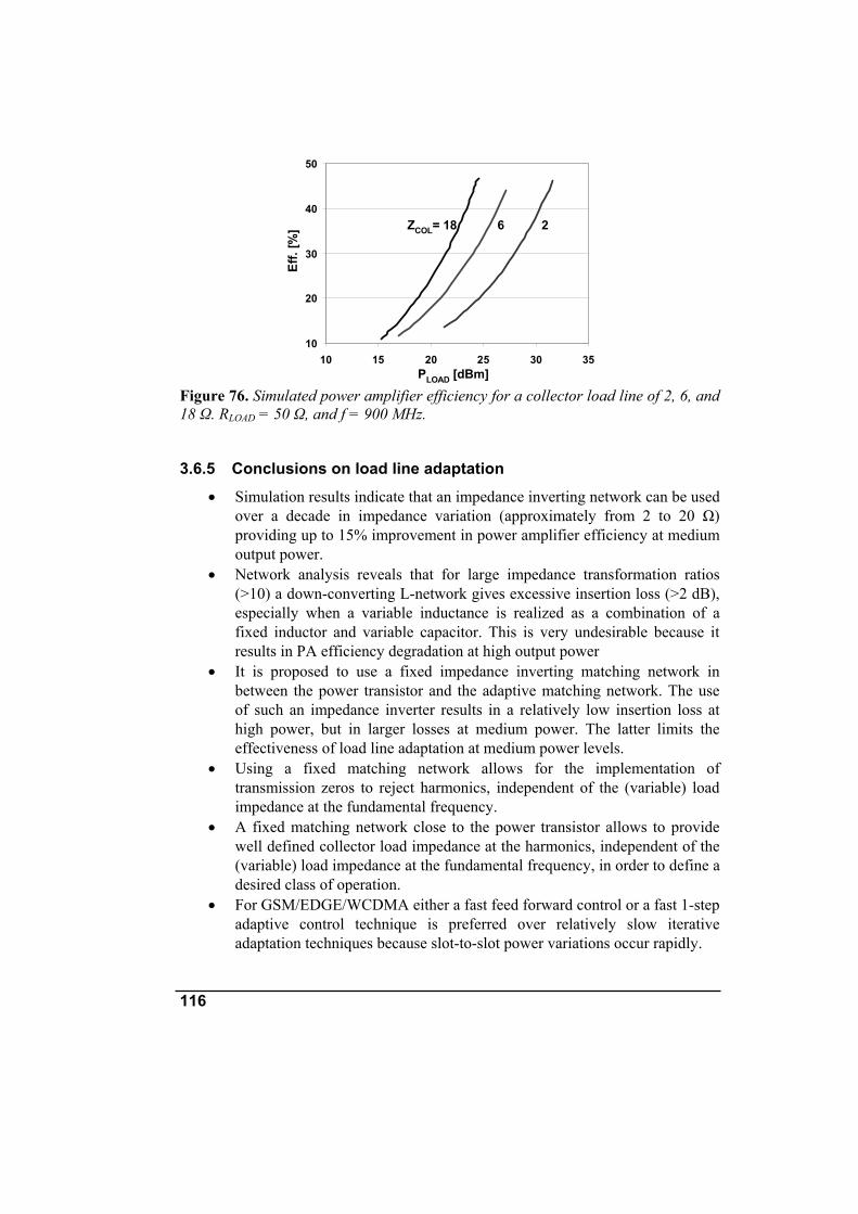
116
10
20
30
40
50
10 15 20 25 30 35PLOAD [dBm]
Eff.
[%] ZCOL= 18 6 2
Figure 76. Simulated power amplifier efficiency for a collector load line of 2, 6, and 18 Ω. RLOAD = 50 Ω, and f = 900 MHz.
3.6.5 Conclusions on load line adaptation
• Simulation results indicate that an impedance inverting network can be used over a decade in impedance variation (approximately from 2 to 20 Ω) providing up to 15% improvement in power amplifier efficiency at medium output power.
• Network analysis reveals that for large impedance transformation ratios (>10) a down-converting L-network gives excessive insertion loss (>2 dB), especially when a variable inductance is realized as a combination of a fixed inductor and variable capacitor. This is very undesirable because it results in PA efficiency degradation at high output power
• It is proposed to use a fixed impedance inverting matching network in between the power transistor and the adaptive matching network. The use of such an impedance inverter results in a relatively low insertion loss at high power, but in larger losses at medium power. The latter limits the effectiveness of load line adaptation at medium power levels.
• Using a fixed matching network allows for the implementation of transmission zeros to reject harmonics, independent of the (variable) load impedance at the fundamental frequency.
• A fixed matching network close to the power transistor allows to provide well defined collector load impedance at the harmonics, independent of the (variable) load impedance at the fundamental frequency, in order to define a desired class of operation.
• For GSM/EDGE/WCDMA either a fast feed forward control or a fast 1-step adaptive control technique is preferred over relatively slow iterative adaptation techniques because slot-to-slot power variations occur rapidly.

117
3.7 Conclusions on adaptive impedance control • Adaptive impedance matching techniques are presented, which provide
resilience to fluctuations in antenna impedance caused by changes in antenna environment due to varying body-effects and changes in phone form-factor.
• Robust control of matching networks over a large impedance region is
shown to be challenging because: o It requires control in two dimensions (real and imaginary),
basically because impedance is two-dimensional. o The impedance transformation of matching networks is a high-
order non-linear function of multiple independent variables (tunable capacitor values) in two dimensions (real and imaginary), which results in
o Multiple solutions causing ambiguousness in control.
• Two robust adaptive impedance matching techniques are presented which make use of simplified network tunability for direct control of variable capacitors:
I. Differentially controlled capacitors (or inductor) for tuning PI- and T-networks. This results in pseudo-orthogonal control, over a wide impedance region, by only two independent variables, which is the minimum for two-dimensional control. Differential control is applied to single-section and dual-section networks.
II. Cascading two loops for controlling up- and down-converting L-networks. It provides independent control of the real and imaginary part of the impedance.
• These techniques make use of a priori knowledge on network tuning
properties (e.g. the sign of the control curve slope) for direct control of variable capacitors, without a need for gradient search or software computation.
• A novel true-orthogonal detector is presented, which provides power and
modulation independent mismatch information in the impedance, admittance, or reflection coefficient domain.
• For load line modulation, a fixed impedance inverting matching network is
proposed in between the power transistor and the adaptive matching network in order to reduce insertion loss of the tunable network at maximum output power.


119
Chapter
4 Adaptive power control
4.1 Introduction Cellular phone power amplifiers usually operate in strongly fluctuating
environments. The output power varies over a wide range to compensate for fluctuations in propagation path loss. The collector load impedance varies due to fluctuations in antenna body-effects [14], [15] and it varies as a function of the transmitting frequency due to the narrow bandwidth of miniaturized antennas. In addition, the supply voltage changes due to charging and de-charging of the battery. At high output power and extreme operating conditions the power transistor suffers form avalanche, self-heating and distortion due to saturation. Usually, large margins are built-in, by design and technology, in order to prevent the transistor from avalanche breakdown, thermal run-away, and severe clipping. Inevitably, these large margins deteriorate RF performance and come with additional costs in packaging, chip area, and IC-technology.
As an alternative solution, this Chapter presents adaptive power control techniques that make power amplifiers resilient to fluctuations in the operating environment. They provide a limitation in power transistor input power once a detected parameter crosses an a priori defined threshold level. These adaptive techniques have been investigated in order to achieve the following goals:
• Ruggedness improvement by o Over-voltage protection to prevent avalanche breakdown o Over-temperature protection to prevent thermal run-away
• Linearity improvement by o Under-voltage protection to avoid saturation
In the following Sections, each of these goals are introduced in more detail.
4.1.1 Over-voltage protection for improved ruggedness Avalanche breakdown of a power transistor [80]-[82], is caused by an excessively
high voltage across the collector-base junction. To prevent avalanche breakdown,

120
power transistors are commonly implemented in an IC-technology with high breakdown voltages (typically BVCBO ~ 20 V for GSM PAs). This is achieved by using a relatively thick epi-layer in case of a silicon transistor (or thick mesa-layer in case of a GaAs HBT device) and by optimizing the collector doping profile. However, such a ruggedness optimization inevitably results in a reduction of the fT, and consequently, in a lower gain-bandwidth product of the power transistor and thus in a lower PA efficiency [83].
By adopting over-voltage protection circuits, that prevent avalanche breakdown under extremes [84]-[30], the trade-off between fT and breakdown voltage can be shifted towards improved performance under nominal operating conditions. It enables the use of a low cost main-stream silicon IC-technology (with lower breakdown voltages) for integration of rugged power amplifiers, including biasing circuits, power control functions and control logic, that are competitive to GaAs HBT implementations. Related work has been reported in [86] and [87].
To prove the feasibility of over-voltage protection hardware prototypes have been realized and the investigation results are reported in Section 4.3.6.1.
4.1.2 Over-temperature protection for improved ruggedness Electro-thermal instability of a bipolar power transistor is mainly caused by self-
heating [37]-[89]. In power amplifier module design several countermeasures are usually taken against thermal run-away like the use of emitter and/or base-degeneration resistors, heat spreading interconnect, exposed heat sinks, plated and/or copper filled laminate vias, and proper distribution of RF load and source impedances over the entire transistor array. All these measures are aiming for a reduction in die temperature, and for a reduction in temperature differences between transistors in the array. Moreover, as over-heating accelerates failure mechanisms, these measures also increase product life-time. Major disadvantages of these countermeasures are associated packaging cost and size and reduced efficiency in case of emitter degeneration.
However, when extreme temperatures are avoided by using over-temperature protection circuits, RF front-end modules with higher thermal package resistance and thus lower cost and smaller form factors can be applied.
To prove the feasibility of over-temperature protection similar prototypes have been realized as for over-voltage protection and the results are reported in Section 4.3.6.2.
121
4.1.3 Under-voltage protection for improved linearity Bandwidth efficient modulation schemes impose, due to their non-constant
envelope, requirements on the linearity of power amplifiers [90]. Under extremes, saturation of a bipolar transistor causes hard clipping of the collector voltage, which results in strong deterioration of the Error Vector Magnitude (EVM) and Adjacent Channel Power Ratio (ACPR) when no precautions are taken.
Especially in single-band cdmaOne phones, isolators are used to preserve power amplifier linearity under extremes. This prevents the transistor from saturating by dissipating the reflected power in a load resistor that terminates the isolator third port [91]. However, for multi-band phones, the use of isolators is not attractive because, due to their narrow bandwidth, multiple isolators are required that are bulky and cannot easily be integrated with other front-end functions. Hence, to achieve cost and size reduction, load-insensitive PA and transceiver concepts are of great interest to handset manufacturers [92], [93].
As an alternative solution, under-voltage protection circuits are proposed that reduce distortion under extremes and can be realized at low cost. To prove the feasibility of under-voltage protection a hardware demonstrator has been realized and the investigation results are reported in Section 4.4.

122
4.2 Safe operating conditions In 2005, Vanhoucke and Hurkx formulated a unified electro-thermal stability
criterion for bipolar transistors [80]. Similar work has been presented by Lee in [81]. They quantified the maximum allowable DC operating conditions bounded by avalanche multiplication and electro-thermal instability that leads towards thermal break-down, often referred to as thermal run-away. It manifests itself in snap-back of the transistor output characteristic, in pinch-in of the current in to the center of a single emitter finger, and in contraction of the current in one of the fingers of a multi-finger structure, as described in [94] and [82].
The unified stability criterion, presented in [80], defines the critical collector current IC_CRIT as :
EQTHEQn
TnCRITC URRM
UMI
⋅−−=
ϕ, (126)
in which
n
CBO
CB
n
BVU
M
−
=
1
1, (127)
q
kTU j
T = ,
(128)
))1(1(0
−−+
+= nn
BEEEQ M
MRR
RRβ
, (129)
))1(1(0
−−+= nn
BECEEQ M
MU
UUβ
, (130)
)( BBECCETHAMBj IUIURTT ++= , (131)
in which: Mn Avalanche multiplication factor UT Thermal voltage kTj/q REQ Equivalent resistance, UEQ Equivalent voltage, RTH Thermal resistance φ Base-emitter temperature dependency (~ -1mV/˚C)

123
BVCBO Collector-base breakdown voltage for shorted base-emitter n Technology dependent constant, typically 3 .. 4 for silicon RE Emitter resistance representing internal and external resistances, RB Base resistance representing internal and external resistances UCE Collector-emitter voltage UBE Base-emitter voltage UCB Collector-base voltage βo Transistor current gain Tj Junction temperature TAMB Ambient temperature
The avalanche multiplication factor Mn [95], [96] is often determined empirically
and can be approached by (127). Figure 77 gives an illustration of critical collector currents as a function of the
collector-emitter voltage for representative parameter values of a 4W GSM power transistor, according to (126).
Figure 77a shows curves of critical currents for RE = 75, 100, and 125 mΩ. These curves clearly illustrate that an increase in RE results in a significant increase in critical current for low voltages, but has no influence on the critical current for high voltages. For low collector voltages, RE provides improved stability for both thermal and avalanche effects. For high collector voltages the critical current is independent of RE because, firstly, the avalanche effects are dominated by the base resistance RB, and secondly, thermal effects are small due to low dissipation.
The curves in Figure 77b show the dependency of critical currents on the thermal resistance RTH. The larger the thermal resistance, the small the critical current is.
Figure 77c show the impact of the base resistance RB. For low collector voltages RB stabilizes the transistor, since it improves the thermal stability, but for high collector voltages RB makes the transistor less stable because it enhances avalanche. The point of intersection is at the collector-base break-down voltage for open base BVCEO (see Appendix C).
The influence of the breakdown voltage BVCBO on critical currents is shown in Figure 77d. It illustrates that the critical current increases with increasing breakdown voltage over a relatively wide voltage range.

124
0,0
1,0
2,0
3,0
2 4 6 8 10
UCE [V]
ICR
IT [A
]
RB = 1, 3, 10 Ohm
0,0
1,0
2,0
3,0
2 4 6 8 10
UCE [V]IC
RIT
[A]
BVCBO = 14, 18, 22 V
0,0
1,0
2,0
3,0
2 4 6 8 10
UCE [V]
ICR
IT [A
]
RTH = 20, 25, 30 K/W
0,0
1,0
2,0
3,0
2 4 6 8 10
UCE [V]
ICR
IT [A
]RE = 75m,100m, 125mOhm
(a) (b)
(c) (d)
Figure 77. Critical collector current as a function of the collector voltage defining the safe operating conditions of a bipolar power transistor. Typical values for a 4W GSM power transistor are: RE = 0.1, RB = 3, RTH = 25K/W , BVCBO = 18, φ = -1mV/˚C, βo = 140, n = 3.5, and TAMB = 25˚C.
The well known criteria on avalanche stability and on electro-thermal stability are
now two special cases of the unified criterion, as given by equation (126). For a temperature coefficient φ of zero, the criterion on avalanche stability
becomes
EQ
TCRITC R
UI
−= , (132)
which is very similar to the criterion derived by Rickelt and Rein in [36]. According to this criterion, the transistor becomes instable, when the negative base current, caused by avalanche, creates a voltage across the base resistance that is larger than UT plus the emitter degeneration voltage IE.RE. They describe, at the on-set of avalanche instability, an abrupt pinch-in of the emitter current in to a very small area in the center of the emitter. This pinch-in increases the effective base resistance, which enhances the avalanche instability even further.
Similarly, for an avalanche multiplication factor Mn of 1, the criterion on electro-
thermal stability becomes approximately

125
CETHB
E
TCRITC
URR
R
UI
⋅−+−=
ϕβ
)(0
, (133)
which is very similar to the criterion derived in [37]. According to this criterion the transistor becomes instable, when the base-emitter voltage reduction, due to self-heating RTH.UCE.IC and the negative temperature coefficient φ, is larger than the thermal voltage UT plus the emitter and base degeneration voltage IC.(RE+RB/β0). Due to small perturbations, the current contracts to the hottest spot of the transistor, which causes this spot to become even hotter and the device will breakdown destructively.

126
4.3 Power adaptation for ruggedness
4.3.1 Concept To improve the ruggedness of RF front-ends, a generic protection concept has
been developed that is based on adaptive power control [97]-[99]. In principle, this concept can be used for over-voltage, under-voltage, over-temperature, and/or over-current protection. Moreover, it can be applied in open-loop as well as in closed-loop power controlled PAs. A voltage detector, temperature detector and/or current detector are used to monitor the maximum collector peak voltage, the minimum collector peak voltage, the die temperature and/or the collector current respectively. Once a detected parameter value crosses a pre-defined threshold level the effective power control voltage is reduced to limit the output power10.
The adaptive control loops, used to provide protection, are made part of the phone power control loop (PCL) in order to avoid opposite control of the PCL and that of the protection circuits, which might occur when protection circuits, based on local feedback, limit the output power under extremes, while the power control loop tries to increase it up to the requested level.
Figure 78. Block diagram of an over-voltage and over-temperature protected power amplifier based on adaptive control of the power transistor input power.
10 To control mobile phone output power two different methods are commonly used. In high-efficiency GSM power amplifiers usually the amplifier gain is made variable by controlling the bias currents of the power transistor driver stages. The input power PIN to the power amplifier is kept constant by the transceiver.
In highly linear EDGE and W-CDMA power amplifiers the gain is usually kept fixed in order to meet linearity requirements. Therefore, power control of phones in linear mode is done by changing the input power PIN of the amplifier by the transceiver.

127
A block diagram of the proposed concept is depicted in Figure 78. The PA consists of a variable gain amplifier (VGA) driving a power transistor T1 which delivers power to the (antenna) load impedance ZLOAD. Detectors (not shown) provide information on detected collector voltage UDET and on detected die temperature TDET. An output power control voltage UDAC is applied externally to set the power PLOAD. Threshold reference voltages for over-voltage protection UREF_OVP
and for over-temperature protection UREF_OTP are applied as input signal to each feed-back loop. U*
DAC represents the adaptively corrected power control voltage. The system transfer function for the detected output power PDET, the detected
collector voltage UDET, and the detected die temperature TDET are given by:
SoLGGUGUUH
U TOTPREFUOVPREFDACUDET +
⋅+⋅+=
1)( __ (134)
and
SoLGGUGUUH
T TOTPREFUOVPREFDACTDET +
⋅+⋅+=
1)( __ , (135)
respectively, in which the sum of loop gains SoLG is given by:
TTUU GHGHSoLG += , (136)
and, the power amplifier voltage and temperature transfer functions HU and HT are respectively defined as:
*DAC
DETU U
UH = and *DAC
DETT U
TH = . (137)
The gain blocks GU and GT represent threshold amplifiers with gains equal to zero when UDET < UREF_OVP and TDET < UREF_OTP (nominal operating conditions) and non-zero when UDET > UREF_OVP and/or TDET > UREF_OTP (under extreme conditions). In the latter case:
DACTOTPREFUOVPREF UGUGU >⋅+⋅ __ (138)
and the parameters UDET and TDET are governed by the protection reference voltages UREF_OVP and/or UREF_OTP rather then by the output power control voltage UDAC. The current IPROT refers to the protection circuit output signals, discussed in the paragraphs 4.3.3 and 4.3.4, and is fed back in to the summation node. AIN represents the power transistor input signal, similar to what is used for the theoretical analysis presented in Chapter 2.
4.3.2 Simulations To verify the feasibility of the adaptive protection concept, discussed in Section
4.3.1, and the validity of the theory on mismatch behavior, presented in Section 2.4,
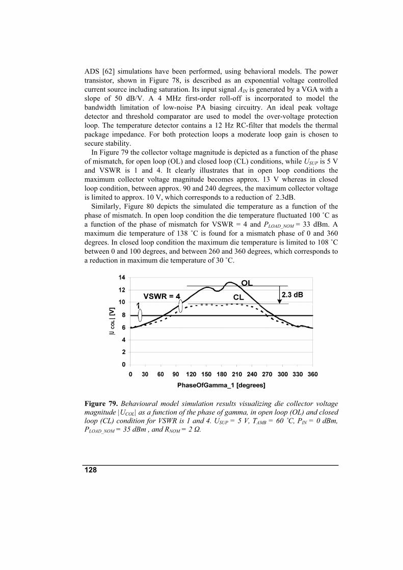
128
ADS [62] simulations have been performed, using behavioral models. The power transistor, shown in Figure 78, is described as an exponential voltage controlled current source including saturation. Its input signal AIN is generated by a VGA with a slope of 50 dB/V. A 4 MHz first-order roll-off is incorporated to model the bandwidth limitation of low-noise PA biasing circuitry. An ideal peak voltage detector and threshold comparator are used to model the over-voltage protection loop. The temperature detector contains a 12 Hz RC-filter that models the thermal package impedance. For both protection loops a moderate loop gain is chosen to secure stability.
In Figure 79 the collector voltage magnitude is depicted as a function of the phase of mismatch, for open loop (OL) and closed loop (CL) conditions, while USUP is 5 V and VSWR is 1 and 4. It clearly illustrates that in open loop conditions the maximum collector voltage magnitude becomes approx. 13 V whereas in closed loop condition, between approx. 90 and 240 degrees, the maximum collector voltage is limited to approx. 10 V, which corresponds to a reduction of 2.3dB.
Similarly, Figure 80 depicts the simulated die temperature as a function of the phase of mismatch. In open loop condition the die temperature fluctuated 100 ˚C as a function of the phase of mismatch for VSWR = 4 and PLOAD_NOM = 33 dBm. A maximum die temperature of 138 ˚C is found for a mismatch phase of 0 and 360 degrees. In closed loop condition the maximum die temperature is limited to 108 ˚C between 0 and 100 degrees, and between 260 and 360 degrees, which corresponds to a reduction in maximum die temperature of 30 ˚C.
Figure 79. Behavioural model simulation results visualizing die collector voltage magnitude |UCOL| as a function of the phase of gamma, in open loop (OL) and closed loop (CL) condition for VSWR is 1 and 4. USUP = 5 V, TAMB = 60 ˚C, PIN = 0 dBm, PLOAD_NOM = 35 dBm , and RNOM = 2 Ω.

129
Figure 80. Behavioural model simulation results visualizing die temperature TDIE , as a function of the phase of gamma, in open loop (OL) and closed loop (CL) condition for VSWR is 1 and 4. USUP = 3.5 V, TAMB = 25 ˚C, PIN = 0 dBm, PLOAD_NOM = 33 dBm, RTH = 37 K/W, and RNOM = 2 Ω.
4.3.3 Over-voltage protection circuit In Figure 81 an over-voltage protection circuit is depicted that consists of a
collector peak voltage detector, connected to power transistor T3, and a succeeding threshold comparator. A capacitive voltage divider with shunt resistors is used to sense both the DC and RF part of the collector voltage. Consequently, the detector output voltage UDET is a function of the battery voltage and of the RF voltage wave amplitude. A NPN collector-base junction diode T5, with high reverse breakdown voltage, is used as detector, charging the filter capacitor during the peaks of the RF voltage. Once the detected voltage UDET crosses a threshold level UREF_OVP, that is applied externally, the comparator output transistor T10 sinks a current IPROT to adapt the PA power control voltage U*
DAC. The power transistor biasing circuit, consisting of T1 and T2, makes use of a diode
D1 and parallel resistor RPAR in order to enhance the breakdown voltage of the power transistor, as elaborated in Appendix C.

130
Figure 81. Circuit diagram of the power transistor T3 with collector peak voltage detector and threshold comparator.
4.3.4 Over-temperature protection circuit For the temperature detector, shown in Figure 82, a differential circuit topology
was chosen to minimize its susceptibility to RF interference, and to obtain an accurate reading of the absolute die temperature [98]. The detector consists of the four diodes D10 … D13, scaled in area by a factor four, and biased by currents, also scaled by a factor four, but in opposite order. It results in a differential detector output voltage UA-UB proportional to the temperature T given by:
)16ln(2 ⋅⋅==−q
kTUUU DETBA . (139)
The factor two stems from the two diodes D10/D11 and D12/D13 placed in series to double the detector sensitivity. The factor ln(16) results from the scaling by four twice. Consequently, the detected voltage is independent of bias currents and process parameters and, consequently, calibration of the detector is not needed. The detector sensitivity DS, given by the derivative of (26), equals 0.48 mV/˚C, because Boltzmann’s constant k = 1.38e-23 J/K and the electric charge q = 1.60e-19 C. The detected voltage is fed to a comparator circuit T12...T15 that activates its output buffer transistor T16 when the comparator input voltage crosses zero. The detector threshold level is set by the differential offset voltage generated across the two threshold resistors RTHR and threshold currents ITHR. The reference voltage UREF is applied externally and controls a simple V/I-converter (T10, T11, and R10) to generate this current.

131
Figure 82. Circuit diagram of the temperature detector and threshold comparator with adjustable threshold.
4.3.5 Technology The active circuits have been processed in Qubic4+, which is a standard 0.25 µm
BiCMOS technology [101] that offers a high voltage NPN (HV-NPN) with a collector-emitter breakdown voltage BVCEO of 6 V and a collector-base breakdown voltage BVCBO of 18 V, with a peak fT of approx. 26 GHz. The active die is flip-chipped on a passive silicon (PASSI) die with a high-ohmic (5 kΩ.cm) low loss substrate [87] as shown in Figure 83 and Figure 84. The PASSI technology provides high-Q Metal-Insulator-Metal (MIM) capacitors with a high breakdown voltage (200 V) for the implementation of rugged, low loss, matching networks, and a high-density capacitor (25 nF/mm2) for supply decoupling. Plated through-wafer vias are used to connect top metal layers with the back-side metal for proper RF and DC-grounding of the power transistor, supply decoupling capacitors and matching capacitors. Its 5 µm thick top metal layer is well suited for implementation of low loss inductors and power routing. The good thermal conductance of the relatively large, heat spreading, PASSI die ensures a low thermal resistance.
4.3.6 Experimental verification The ruggedness of a 4 W power transistor, shown in Figure 83 and Figure 84, is
verified for continuous as well as for pulsed excitations at 900 MHz. The test set-up, depicted in
Figure 85, comprises quarter-lambda micro strip lines and manually controlled slug-tuners to match the power transistor input and output. A nominal load-line is chosen in-between that for maximum efficiency (~80%) and that for maximum power gain (~16 dB). An attenuator and RF-short with variable length define the mismatch. A three stage power amplifier (BGY288) is used as driver for the power transistor. The protection circuit output current IPROT is externally fed back, via a resistor RDAC, to adapt the power control voltage U*
DAC of this driver amplifier.

132
Figure 83. Photograph of an active die, containing the power transistor, biasing circuits, and detectors, flip-chipped on a passive die wire-bonded to laminate.
Outputmatch
Input match
4 W powertransistor
Biasing
Protections
BiCMOS diePASSI die
Figure 84. Photographs of a power transistor die, with integrated biasing and protection circuits, flip-chipped on a passive-silicon die, to be placed on top of, and to be wire-bonded to, a laminate.
SlugtunerSlug tuner A tt
.
A tt.G enerator
10 ohm+M M
50 ohm+M M10 ohm50 ohm
BG Y288w ithPC L
U DAC
R DA C
Iprot
l/4l/4
U *DA C
DU T
Figure 85. RF measurement set-up used to verify the power transistor ruggedness, while it is protected by adaptive power control.

133
4.3.6.1 Over-voltage protection The control voltage UDAC is set to obtain 33dBm output power for a nominal 50 Ω
load and 3.5 V supply. A nominal load-line is chosen in-between that for maximum efficiency (~80%) and that for maximum power gain (~16 dB). Then, the supply is set at 5 V and an extreme VSWR of 10 is applied and the phase of the mismatch varied from 0 to 360 degrees. The measured actuation current IPROT as well as the power dissipated in the load are depicted in Figure 86 for four reference voltages. At 0.8 V actuation occurs over a wide range of mismatch phases and a maximum reduction in output power of 2.7 dB is found at a phase of 300 degrees. This value comes rather close to the simulated 2.3 dB shown in Figure 79. For this condition no destructive breakdown has been observed. It is worthwhile noting that even without adaptive correction (UREF = 1.4 V) some of the devices passed these extreme tests, but many of them did not.
4.3.6.2 Over-temperature protection
In a similar manner the over-temperature protection loop is tested. Figure 87 shows, for a VSWR of 4, the power delivered to the load PLOAD for three different over-temperature reference voltages. Relatively strong actuation (power reduction) is obtained over a wide phase range for UREF_OTP = 1.1 V, whereas no actuation takes place for mismatch phases (of low dissipation) between 180 and 270 degrees. At UREF_OTP = 1.4 V the loop does not activate at all and the die temperature fluctuates approx. 100 ˚C as a function of the phase of mismatch. A maximum die temperature of 143 ˚C is found at a mismatch phase of 30 degrees, which is reduced to 112 ˚C when UREF_OTP is set at 1.2 V, as is shown in Figure 87 at the right hand-side Y-axis. Note, that this reduction in maximum die temperature of 31 ˚C corresponds well with simulation data of Figure 80.
For the same conditions the power dissipated in the transistor reduces from 3.25 W to 2.4 and 2.0 W respectively. It is worthwhile noting that a very good correlation is found between dissipated power and adaptive power correction.
For pulsed conditions the adapted power control voltage U*DAC of the protection
loop is shown in Figure 88 for three different reference voltages. For UREF = 0.9 V (upper curve) no actuation occurs. The rising and falling edges of the protection loop has been investigated in detail. Both response times are well within 10 µs, which is sufficient to fulfill GSM power burst requirements.

134
Figure 86. Measured actuation current IPROT and output power PLOAD as a function of the phase of mismatch for reference voltages of 0.8, 1.0, 1.2, and 1.4 V. VSWR = 10, USUP = 5 V.
Figure 87. Adaptively controlled output power PLOAD and calculated die temperature as a function of the phase of mismatch. Over-temperature is used as control criterion by setting UREF_OTP at 1.1, 1.2, and 1.4V.

135
Figure 88. A fast protection loop response time is illustrated by the adapted power control voltage U*DAC as a function of time measured for three different reference voltages.

136
4.4 Power adaptation for linearity
4.4.1 Concept To avoid collector voltage saturation under antenna mismatch conditions an
adaptively controlled power amplifier is used as depicted in Figure 89. Except for the Track-and-Hold (T&H) circuit, the concept is similar to that of the over-voltage and over-temperature protection circuits. The minimum collector peak voltage is monitored by a diode peak detector. When this detected minimum voltage falls below the under-voltage protection threshold voltage UREF_UVP the Track-and-Hold circuit is triggered to increase its output voltage. Consequently, the gain of the variable gain pre-amplifier, commonly present at the PA input to control the power transistor output power, is slightly reduced. This gain reduction limits the amplitude of the collector RF voltage and thus prevents saturation of the power transistor.
UDAC
UDET
PA
Uref_UVPT&H
ZLOAD
U*DAC
PLOAD
VGAT1
HUAIN
PIN
Figure 89. Power amplifier using adaptive power control to avoid collector voltage saturation.
4.4.2 Simulations To verify the effectiveness of this adaptive method in preserving linearity,
simulations are performed using behavioral models. The RF-transistor is modeled as a voltage controlled current source according to the exponential behavior of a bipolar transistor. The model includes the base-collector junction behavior to represent collector voltage saturation. Time domain analysis results show the adaptation of the magnitude of the lower-side envelope of an EDGE modulated collector voltage [102] that can be expressed as:
)))()(arctan(.cos(.)()()( 0
22
tItQttQtIVtv Supplycol +++= ω (140)
for time moments t at which the term cos(...) equals -1. I(t) and Q(t) represent the complex base-band signals modulating the carrier frequency ω0.

137
Using envelope simulations, we initially determined the input power required to obtain a nominal output power of 28.6 dBm in a 50 Ω load. The load impedance ZLOAD was changed to represent a VSWR of 4 at the output of the matching network. The worst-case phase of the mismatch was chosen such that a maximum collector load impedance occurs, corresponding to a reflection coefficient phase of zero degrees at the collector, as derived in Section 2.4. Figure 90 depicts the resulting lower-side envelope of the EDGE modulated collector voltage for an open, as well as closed, adaptive loop. The hard clipping that occurs in open loop is avoided once the loop is closed. The supply voltage is 3.5 V. On the right-hand-side Y-axis the gain reduction of the variable gain amplifier (VGA) is shown. We can clearly see the fast attack of the loop during the first 20 µs, as well as the ripple that is caused by peaks in the envelope re-activating the Track-and-Hold circuit. The corresponding spectra, given in Figure 91, show an impressive improvement in spectral re-growth.
With a Harmonic Balance simulation the behavior of the adaptive loop has been studied as a function of the phase of the mismatch as depicted in Figure 92. The VGA control voltage, VCONTROL_VGA, reduces the gain by 4 dB/V. Obviously, the larger the VSWR the wider the range of phases over which the loop is activated to prevent the RF-transistor from saturating.
Figure 90. Simulated difference in the lower-side collector voltage envelope for open loop and a closed loop adapting the power. The corresponding VGA gain reduction is on the right-hand-side Y-axis. VSWR = 4, phase of ΓCOL = 0 degrees.

138
Figure 91. Simulated difference in spectral re-growth between open loop and a closed loop adapting the power VSWR = 4, phase of ΓCOL = 0 degrees.
Figure 92. The simulated VGA control voltage as a function of the load mismatch phase shows that the loop is activated over a limited range of mismatch phases. VSWR = 1, 2, 3, and 4.

139
4.4.3 Circuit design In order to proof the feasibility of an adaptively controlled power amplifier,
hardware has been realized. The circuit diagram in Figure 93 depicts a three-stage power amplifier module (PAM) using a control loop that adaptively adjusts the output power of the amplifier. The detector output voltage, VDETECTOR, representing the envelope of the minimum collector voltage of the last RF-stage, is fed to a voltage follower and comparator amplifier with a manually adjustable threshold voltage VREF. This comparator controls the resistance of a MOS-transistor, used to rapidly charge the capacitor CHOLD once the threshold level is crossed. A buffer amplifier controls the gain of the variable gain driving amplifier BGA2031, to reduce its gain when the loop is activated.
Figure 93. Power amplifier module (PAM) embedded in a control loop to adaptively preserve PA linearity under mismatch.
The potentiometers P1 and P2 set the total variable gain range to approximately
10 dB, of which approximately 5 dB is actually used. The component values are chosen such that acquisition of the loop occurs well within one symbol period, whereas the decay time is made large to prevent the loop from re-introducing any amplitude distortion. Also the peak detector is weakly coupled to the RF-path in order to avoid introduction of distortion.
The power amplifier module consists of two, fully independent, RF line-ups. For

140
these experiments it has been populated for the 900 MHz band only, as is shown in Figure 94. The first and second RF-stage are integrated into a 0.5 µm silicon bipolar driver IC that is visible on the right-hand side. The power transistor and the minimum collector voltage peak detector are integrated into a second silicon die. On the left-hand side of the module the output matching network and the feeding choke with supply decoupling capacitors are visible. The module uses a 5-layer LTCC as substrate that measures 11 mm x 13.75 mm [103].
Figure 94. Hardware demonstrator of the adaptively controlled PAM preserving linearity by avoiding collector voltage saturation under mismatch.
4.4.4 Experimental verification To verify the relationship between distortion and collector voltage saturation, load
pull measurements have been performed on the PAM in open loop. The measured Error Vector Magnitude (EVM) and the detected voltage contours of VDETECTOR are depicted in Figure 95.
The dotted circle, centered around the nominal load impedance of 50 Ω, represents a VSWR of 4. The closed contours near the center of the Smith chart show an optimum EVM of approximately 4%, whereas the dense EVM contours at the lower right part of the chart indicate significant distortion. The EVM contours are displayed with a step size of 1%. The voltage detector contours are approximately equally spaced over the entire Smith chart with maximum values in the upper left corner and minimum values in the lower right corner. Their spacing is 0.1 V. There is a strong correlation between maximum EVM and minimum detected collector voltage, as expected.

141
Figure 95. Measured EVM and minimum collector peak voltage show a strong correlation. PLOAD = 28.5 dBm, f = 900 MHz, and VSWR = 4.
Open loop as well as closed loop EVM and ACPR measurements are carried out
for an EDGE modulated signal. Initially, the output power is set at 28.5 dBm in a 50 Ω load by choosing the input power appropriately. A load mismatch is then applied with a VSWR of 4 while the phase of the mismatch is varied over 360 degrees. The measured EVM, depicted in Figure 96, has a maximum at 180 degrees. By closing the adaptive control loop the maximum EVM is reduced from approximately 15% to 10%.
Figure 97 shows the measured ACPR for the same conditions. At 180 degrees the ACPR improves from approximately –43 dBc to –55 dBc by closing the loop. The loop reference voltage was set at approximately 0.9 V. For this chosen value, the loop activates the BGA2031 for mismatch phases between approximately 135 and 270 degrees. It reduces the VGA gain with a maximum of approximately 4.5 dB at 180 degrees mismatch, which is just sufficient to keep the PA out of strong saturation.

142
Figure 96. EVM measured as a function of the phase of mismatch for open and closed loop. VSWR = 4. PLOAD is set at 28.5 dBm at 50 Ω.
Figure 97. ACPR measured as a function of the phase of mismatch for the same conditions.

143
4.5 Conclusions on adaptive power control • In order to improve power amplifier ruggedness and to preserve its
linearity under extreme operating conditions a generic protection concept has been developed that is based on adaptive control of power.
• This concept provides over-voltage, over-temperature, and/or under-
voltage protection by detection of the maximum collector peak voltage, die temperature, and/or minimum collector peak voltage to limit the power transistor input power once a threshold level is crossed.
On ruggedness:
• To prove adaptive power control a feasible technique in avoiding over-voltage and over-temperature conditions, a silicon bipolar power transistor and over-voltage and over-temperature protection circuits have been integrated in Qubic-4+ technology.
• The over-voltage protection circuit is investigated for a PA supply voltage
of 5 V and a nominal output power of 2 W. No breakdown is observed for a VSWR of 10 over all phases when the output power is adaptively reduced by 2.7 dB at most. It is worthwhile noting that even without adaptive correction some of the devices passed these extreme tests, but many of them did not.
• The over-temperature protection circuit is investigated at a nominal PA
supply voltage of 3.5 V. For a VSWR of 4 the maximum die temperature is reduced from 143 ˚C to 112 ˚C when the output power is adaptively reduced from 32.1 dBm to 27.7 dBm.
• These measurement results provide strong evidence that power transistors
can be implemented in low-cost silicon technology by applying over-voltage and over-temperature protection circuits.

144
On linearity: • To prove adaptive power control a feasible technique in preserving
linearity under mismatch, a silicon bipolar power transistor including an under-voltage detection circuit has been integrated in MOBI-3 technology.
• A Track-and-Hold circuit, which holds the detected minimum voltage
over a period that is long compared to the intervals in modulation peaks, is applied in order to prevent re-introduction of distortion.
• Measurements show a strong correlation between the detected minimum
peak collector voltage and power amplifier non-linearity, as expected.
• Measurements on an EDGE power amplifier demonstrate an EVM improvement from 15 to 10% and an ACPR improvement from -43 to –55 dBc at maximum power and an VSWR of 4 at worst-case mismatch phase.
• These measurement results prove adaptive power control to be effective in
preserving linearity under mismatch.

145
Chapter
5 Conclusions
The conclusions drawn from this thesis work are the following:
• Adaptive control is proven a feasible method in improving the performance of mobile phone RF front-ends that operate in unpredictably changing environments.
• Robust adaptive impedance control of PI- and L-networks is achieved over
wide impedance regions. Robustness is obtained from newly developed control techniques that are based on:
o Differentially controlled capacitors for tuning PI-networks o Two cascaded loops for controlling L-networks
Both methods make use of a novel true-orthogonal two-dimensional mismatch detector. A hardware demonstrator of an adaptively controlled series-LC impedance matching network has been realized using RF-MEMS devices, which effectively compensates antenna de-tuning caused by hand-effects.
• Power amplifiers, implemented in standard silicon IC-technology, are made
resilient to changing environments by applying adaptive power control. Adaptive power control is generalized as a method to improve power amplifier ruggedness and to preserve its linearity under extremes.
o Avalanche breakdown of a power transistor is avoided by over-voltage protection, using detection of the maximum collector voltage as an indication of potential avalanche instability.
o Excessive dissipation of a power transistor is avoided by over-temperature protection, using detection of die temperature as an indication of potential thermal instability.
o Distortion due to clipping of the power transistor is avoided by under-voltage protection, using detection of the minimum collector voltage as an indication of saturation.

146
Protection is obtained from limiting the power transistor input power when the detected value exceeds a pre-defined threshold. This power limitation reduces maximum radiated power, under extremes, which is a disadvantage of this approach. Power amplifiers have been realized demonstrating good ruggedness and improved linearity under extreme operating conditions.

147
Recommendations
The following future research topics on adaptive RF front-ends are recommended:
• Wide-band adaptive impedance matching techniques need to be developed that provide good Rx/Tx trade-offs, especially for frequency division duplex (FDD) systems, because the separation between Rx and Tx frequencies can be wide apart.
• To accommodate the wide range of operating conditions of an RF front-
end, combinations of supply voltage adaptation, impedance adaptation and/or power adaptation should be investigated in order to increase the dynamic range in control.
• Network topologies with combined re-configurability and tunability need to
be investigated for the realisation of generically applicable (antenna independent) adaptive impedance matching networks.
• Prospects of semiconductor switches need to be explored for co-integration
of adaptive matching networks with Rx/Tx antenna switches and switches for power amplifier load line modulation techniques, which will pave the way for digitally controlled adaptive RF front-ends that are highly miniaturized.
• Adaptive power control techniques for over-voltage, over-temperature,
and/or under-voltage protection can be applied to LDMOS and CMOS power amplifiers in order to relax requirements on their design.


149
Original contributions Original contributions of this thesis work are the following:
• A mathematical analysis is presented describing the impact of the fluctuating environmental parameters: load impedance, supply voltage, and ambient temperature, on the collector voltage, collector current, power dissipation, die temperature, and efficiency of a bipolar power transistor.
• Differentially controlled capacitors are proposed as a new technique for
tuning PI and T-networks with three variable branches. It results in pseudo-orthogonal tuning properties, which simplifies the algorithms required for adaptive control.
• A new adaptive matching technique is developed for the control of L-
networks with two variable branches. It uses a cascade of two independent loops providing true-orthogonal control properties.
• A novel generic quadrature detection method is proposed, which detects the
complex value of either impedance, admittance or reflection coefficient. The detected values are independent of the complex modulation of the RF carrier. The detector uses an inductor or capacitor of the matching network as sensing element for detection in the impedance domain.
• To the author’s knowledge, world’s first switched capacitor RF-MEMS
based adaptive antenna matching module for mobile phone applications is presented.
• The use of adaptive output power control is generalized as a method to
improve power amplifier ruggedness by protecting the power transistor against over-voltage and over-temperature conditions, as well as to improve power amplifier linearity, under mismatch conditions, by protecting the power transistor against under-voltage conditions.


151
Publications Journal papers A. van Bezooijen, M. A. de Jongh, F. van Straten, R. Mahmoudi, A. H. M. van Roermund, “Adaptive impedance matching techniques for controlling L-networks,” Accepted for publication in TCAS-Part I. A. van Bezooijen, M. A. de Jongh, C. Chanlo, L. Ruijs, F. van Straten, R. Mahmoudi, A. H. M. van Roermund, “A GSM/EDGE/WCDMA adaptive series-LC matching network using RF-MEMS switches,” IEEE Journal of Solid-State Circuits, vol. 43, no. 10, pp. 2259-2268, Oct. 2008. A. van Bezooijen, F. van Straten, R. Mahmoudi, A. H. M. van Roermund, “Power amplifier protection by adaptive output power control,” IEEE Journal of Solid-State Circuits, vol. 42, no. 9, pp. 1834-1841, Sep. 2007. A. van Bezooijen, R. Mahmoudi, A. H. M. van Roermund, “Adaptive methods to preserve power amplifier linearity under antenna mismatch conditions,” IEEE Transactions on Circuits and Systems part-1, vol. 52, no. 10, pp. 2101-2108, Oct. 2005. Conference papers A. van Bezooijen, M. de Jongh, C. Chanlo, L. Ruijs, H. J. ten Dolle, P. Lok, F. van Straten, J. Sneep, R. Mahmoudi, and A.H.M. van Roermund, “RF-MEMS based adaptive antenna matching module,” IEEE Radio Frequency Integrated Circuits Symposium Digest, pp. 573-576, Jun. 2007. A. van Bezooijen, F. van Straten, R. Mahmoudi, A.H.M. van Roermund, “Over-temperature protection by adaptive output power control,” IEEE Proceedings of the 36th European Microwave Conference, pp. 1645-1647, Sept. 2006. A. van Bezooijen, F. van Straten, R. Mahmoudi, A.H.M. van Roermund, “Avalanche breakdown protection by adaptive output power control,” IEEE RSW Proceedings, pp. 519-522, Jan. 2006. A. van Bezooijen, R. Mahmoudi, A. H. M. van Roermund, “Adaptive Power Amplifiers Concepts Preserving Linearity under Severe Mismatch Conditions,” IEEE Topical Workshop on Power Amplifiers for Wireless Communications Technical Digest, Sept. 2004.
152
A. van Bezooijen, C. Chanlo, R. Mahmoudi, A. H. M. van Roermund, “Adaptively preserving power amplifier linearity under antenna mismatch,” IEEE MTT-S Int. Microwave Symp. Dig., Vol. 3. pp 1515 - 1518, June 2004. A. van Bezooijen, D. Prikhodko, “Biasing circuits for voltage controlled GSM power amplifiers,” IEEE Proceedings of the 33th European Microwave Conference, pp. 277-280, Oct. 2003. Co-authorships A. van Roermund, P. Baltus, A. van Bezooijen, J. Hegt, E. Lopelli, R. Mahmoudi, G. Radulov, M. Vidojkovic, “Smart front-ends, from vision to design,” IEICE transactions on fundamentals of electronics, communications and computer sciences, vol. E92-C, no. 6, pp. 747 – 756, Jun. 2009. A. J. M. de Graauw, A. van Bezooijen, C. Chanlo, A. den Dekker, J. Dijkhuis, S. Pramm, and H. J. ten Dolle, “Miniaturized quad-band front-end module for GSM using Si BiCMOS and passive integration technologies,” IEEE Proceedings BCTM 2006, pp. 21-24, Oct. 2006. A. J. M. de Graauw, P.G. Steeneken, C. Chanlo, S. Pramm, A. van Bezooijen, H. K. J. ten Dolle, F. van Straten, and P. Lok, “MEMS-based reconfigurable multi-band BiCMOS power amplifier,” IEEE Proceedings BCTM 2006, pp. 17-20, Oct. 2006. F. Meng, A. van Bezooijen, R. Mahmoudi, “A mismatch detector for adaptive impedance matching”, Conference Proceedings of the 36th European Microwave Conference, pp. 1457-1460, Sep. 2006. L. Ruijs, A. van Bezooijen, R. Mahmoudi, A. H. M. van Roermund, “Novel voltage limiting concept for avalanche breakdown protection,” IEEE MTT-S Int. Microwave Symp. Dig., pp. 1842-1845, June 2006. P. Baltus, A. van Bezooijen, “Design considerations for RF power amplifiers demonstrated through a GSM/EDGE power amplifier module,” 10th Workshop on Advances in Analogue Circuit Design, AACD2001, Noordwijk, The Netherlands, April 2001.

153
Workshops A. van Bezooijen, ”Adaptive antenna match using MEMS,” European microwave week (EuMC/EuMIC/EuWiT) workshop, WWE-6, Oct. 2008. A. van Bezooijen, ”Improvements in power amplifier performance via adaptive antenna matching techniques”, IEEE International microwave symposium workshops, WSJ, Jun. 2008.


155
Patents . EP08162029, 7th Aug. 2008, “Dynamic impedance matching network and method for matching an impedance between a source and a load,” A. van Bezooijen. WO-2008/087583, 15th Jan. 2008, “Switchable capacitor array,” A. van Bezooijen, M. de Jongh. WO-2008/087585, 15th Jan. 2008, “MEMS system,” A. van Bezooijen, J. G. Sneep. WO-2008/087584, 15th Jan. 2008, “MEMS capacitor circuit and method,” A. van Bezooijen, J. G. Sneep, M. de Jongh. WO-2008/007330, 9th July 2007, “Load-line adaptation,” A. van Bezooijen. WO-2006/038167, 29th Sept. 2005, “Impedance detector,” A. van Bezooijen, C. Chanlo. WO-2006/056952, 23th Nov. 2005, “Current limiting circuit for RF power amplifier,” J. Hug, D. Prikhodko, A. van Bezooijen. WO-2006/054246, 16th Nov. 2005, “Device comprising a controlled matching stage,” A. van Bezooijen. WO-2006/054245, 16th Nov. 2005, “Device comprising a load-line coupled to an output of an amplifier stage,” A. van Bezooijen. WO-2006/033052, 14th Sep. 2005, “Peak voltage detection circuit and method,” A. van Bezooijen, R. Koster, R. Heeres, D. Prikhodko, B. Balm. WO-2006/030360, 9th Sept. 2005, “Circuit for detecting the impedance of a load,” A. van Bezooijen, C. Chanlo. WO-2004/112242, 14th June 2004, “Power amplifier with power control loop,” D. Prikhodko, A. van Bezooijen, C. Chanlo, J. Hug, R. Koster. WO-2004/057756, 20st Nov. 2003, “Power amplifier with bias control,” A. van Bezooijen, D. Prikhodko. WO-2004/027990, 4th Aug. 2003, “Preserving linearity of a RF power amplifier,” A. van Bezooijen, C. Chanlo. WO-2004/112239, 15th June 2003, “Output power detection circuit,” D. Prikhodko, A. van Bezooijen, C. Chanlo, J. Hug, R. Koster.

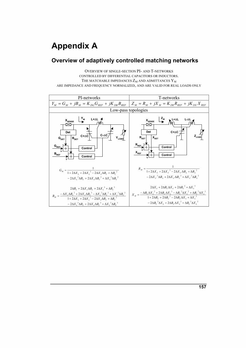
157
Appendix A Overview of adaptively controlled matching networks
OVERVIEW OF SINGLE-SECTION PI- AND T-NETWORKS CONTROLLED BY DIFFERENTIAL CAPACITORS OR INDUCTORS.
THE MATCHABLE IMPEDANCES ZM AND ADMITTANCES YM ARE IMPEDANCE AND FREQUENCY NORMALIZED, AND ARE VALID FOR REAL LOADS ONLY
PI-networks T-networks
REFDBREFDGMMM BjKGKjBGY +=+= REFDXREFDRMMM XjKRKjXRZ +=+=Low-pass topologies
YLOADC+∆C C-∆C
L+∆LYMXSENSE
Det
Control
ControlBREF
GREF
GDET BDET
2222
22
22
22211
CLCLCL
CCLLLM
BXBXBX
BBXXXG
∆∆+∆∆+∆∆−
∆+∆∆−∆+∆+=
2222
22
322232
32
22
22212
222
CLCLCL
CCLLL
CLCLCLCL
CLCLC
M
BXBXBX
BBXXXBXBXBXBX
BXBXB
B
∆∆+∆∆+∆∆−
∆+∆∆−∆+∆+∆∆+∆∆−∆∆+∆∆−
∆+∆+∆∆+∆
=
XSENSE
Det
Control
ControlXREF
RREF
RDET XDET
C+∆C
L+∆LZM L-∆L
ZLOAD
2222
22
22
22211
LCLCLC
LLCCCM
BXBXBX
BBXXXR
∆∆+∆∆+∆∆−
∆+∆∆−∆+∆+=
2222
22
322232
32
22
22212
222
LCLCLC
LLCCC
LCLCLCLC
LCLCL
M
XBXBXB
XXBBBXBXBXBXB
XBXBX
X
∆∆+∆∆+∆∆−
∆+∆∆−∆+∆+∆∆+∆∆−∆∆+∆∆−
∆+∆+∆∆+∆
=

158
PI-networks T-networks
REFDBREFDGMMM BjKGKjBGY +=+=
REFDXREFDRMMM XjKRKjXRZ +=+=
High-pass topologies
XSENSE
Det
Control
ControlBREF
GREF
GDET BDETYLOADL-∆L
YM
L+∆L
C+∆C
2222
22
22
22211
LCLCLC
LLCCCM
BXBXBX
BBXXXG
∆∆+∆∆+∆∆−
∆+∆∆−∆+∆+=
2222
22
322232
32
22
22212
222
LCLCLC
LLCCC
LCLCLCLC
LCLCL
M
BXBXBX
BBXXXBXBXBXBX
BXBXB
B
∆∆+∆∆+∆∆−
∆+∆∆−∆+∆+∆∆+∆∆−∆∆+∆∆−
∆+∆+∆∆+∆
=
XSENSE
Det
Control
ControlXREF
RREF
RDET XDETZLOAD
C+∆C C-∆CZM
L+∆L
2222
22
22
22211
CLCLCL
CCLLLM
XBXBXB
XXBBBR
∆∆+∆∆+∆∆−
∆+∆∆−∆+∆+=
2222
22
322232
32
22
22212
222
CLCLCL
CCLLL
CLCLCLCL
CLCLC
M
XBXBXB
XXBBBXBXBXBXB
XBXBX
X
∆∆+∆∆+∆∆−
∆+∆∆−∆+∆+∆∆+∆∆−∆∆+∆∆−
∆+∆+∆∆+∆
=

159
OVERVIEW OF ADAPTIVELY CONTROLLED DUAL-SECTION PI-NETWORKS
Low-pass topology
YLOAD
C+∆C k(C-∆C)
LYM L
CM+∆CM
XSENSE
Det
Control
ControlBREF
GREF
GDET BDET
REFREFM jBGY +=
High-pass topology
XSENSE
Det
Control
ControlBREF
GREF
GDET BDETYLOAD
L+∆L
CYM C
LM+∆LM k(L-∆L)
REFREFM jBGY +=

160
OVERVIEW OF ADAPTIVELY CONTROLLED DUAL-SECTION T-NETWORKS
Low-pass topology
XSENSE
Det
Control
ControlXREF
RREF
RDET XDETZLOAD
ZM
C
L+∆L LM+∆LM
C
k(L-∆L)
REFREFM jXRZ +=
High-pass topology
ZLOAD
C+∆C k(C-∆C)
L
ZM
L
CM+∆CMXSENSE
Det
Control
ControlXREF
RREF
RDET XDET
REFREFM jXRZ +=

161
OVERVIEW OF ADAPTIVELY CONTROLLED L-NETWORKS
Down-converting L-network
REFREFM jXRZ +=
Up-converting L-network
REFREFM jBGY +=

162
OVERVIEW OF ADAPTIVELY CONTROLLED SERIES-LC AND PARALLEL-LC NETWORKS
Series-LC Parallel-LC
REFLOADM jXRZ += REFLOADM jBGY +=
)1( LOADREFLOAD
REFREFM RG
RGjGY −±=
)1( LOADREFLOAD
REFREFM GR
GRjRZ −±=

163
Appendix B A dual-banding technique
1. Introduction
Multi-band operation might require a matching network that provide a desired impedance transformation at low-band (900 MHz) and high-band (1800 MHz) frequencies, which needs frequency scaling of all inductive and capacitive reactances in the network.
Frequency scaling of an inductance is usually done by short-circuiting parts of the inductor by low-ohmic switches. Unfortunately, RF-MEMS capacitive switches are not very effective in shorting parts of an inductor because the large capacitance required implies the use of a big RF-MEMS device with large parasitics.
Therefore, in this Appendix, we propose an alternative dual-banding technique. Each fixed inductor is replaced by a network of fixed components that provides the desired reactance at two frequency bands (low-band and high-band). The network design equations for this, so-called, dual-band equivalent inductance are derived below. When needed, this network can be extended by a series or parallel variable capacitor to attain some tunability, similar to that of a single inductor.
Frequency scaling of a capacitive reactance in the network can be done by changing the value of a variable capacitor, but requires a relatively large capacitance tuning range because the network needs to provide transformation over a sufficiently large impedance region as well. Fortunately, RF-MEMS switched capacitor arrays provide such a large tuning range.
2. Dual-band equivalent inductance At two different bands, low-band and high-band, a similar impedance
transformation can be accomplished, when the reactances of all network branches are the same for low-band and high-band frequencies.
LSCP
LP Figure 98. Dual-band inductive reactance network

164
The network branch shown in Figure 98 gives the required reactance XL, at low-band as well as at high-band, when (141) holds true.
L
PHBPHB
SHB
PLBPLB
SLB XC
L
LC
L
L =−
+=−
+ω
ω
ωω
ω
ω 11
11
. (141)
We can chose the resonance frequency ωRES of the parallel network in-between the
low-band and high-band frequencies ωLB and ωHB like
PPHBLBres CL
1== ωωω . (142)
The ratio p between the high-band and low-band frequencies of operation can be defined as
LB
HBpωω
= . (143)
Substitution of (141) and (143) in to (141) and rewriting yields
PLBSLBL Lp
pLX ωω1−
+= , (144)
and
PLBSLBL Lp
pLpX ωω1−
−= . (145)
Subtraction of (144) from (145) and rewriting gives
SP Lp
pL2
)1( 2−= . (146)
Further substitution yields
121+
=p
XLLB
LS ω,
)1()1( 2
+−
=pp
pXLLB
LP ω
, and 2)1()1(1
−+
=pp
XC
LLBP ω
, (147)
which gives the component values of a dual-band equivalent inductance XL. For example, for XL = 50 Ω, p = 2.1, and fLB = 870 MHz the required LS equals 5.9 nH, and LP = 1.7 nH, while CP = 8.9 pF, which are realizable component values.

165
Appendix C Transistor breakdown voltages 1. Introduction
This Appendix gives an analysis on the breakdown voltage of a bipolar transistor in relation to the impedance of its biasing circuit at the base. It is shown that biasing circuits can provide an enhancement of the effective breakdown voltage of a power transistor. Basically, the bias circuits are characterized by their ability to sink avalanche current of the bipolar transistor, which results in a shift of the on-set of avalanche breakdown towards a higher collector-base voltage. In this Appendix expressions on transistor breakdown voltages are derived for biasing circuits acting as:
• Shorted source • Open source • Resistor as source • Diode as source • Feedback circuit as source
2. Shorted source
Nx
IAV
IC
IB
UBEUBIAS
USUP
Figure 99. Biasing circuit that consists of a voltage source with an output impedance of zero. The bias voltage UBIAS enforces the base-emitter voltage UBE.
The collector current IC of a bipolar transistor, shown in Figure 99, including
leakage and avalanche breakdown, but neglecting saturation, is commonly described by [67]:
)1)(exp( −⋅⋅=T
BESnC U
UIMI (148)

166
in which Is is the saturation current of the transistor, UT the thermal voltage and Mn the avalanche current multiplication factor. Empirically, it is found that Mn can be expressed as:
n
CBO
CB
n
BVU
M
−
=
1
1, (149)
in which BVCBO is the collector-base breakdown voltage for a shorted base-emitter. The value of η is process dependent and is typically 3…4 for silicon technology. The equation shows that Mn becomes infinite when the collector-base voltage approaches the collector-base breakdown voltage BVCBO, which defines a theoretical limit to the maximum usable collector voltage. Hence, the corresponding maximum collector-emitter break-down voltage BVMAX is given by
CBOBEMAX BVUBV += . (150)
3. Open source
Nx
IAV
IC
IB
UBEIBIAS
USUP
Figure 100. Biasing circuit consisting of a current source with infinite output impedance. The bias current IBIAS enforces the base current IB.
To derive the collector-emitter breakdown voltage for open base, BVCEO, we can rewrite the collector current, given by (148), as the sum of two currents, as
)1)(exp()1()1)(exp( −⋅⋅−+−⋅=T
BESn
T
BESC U
UIM
UU
II . (151)
The first term represents the collector current as a function of the base emitter voltage and the second term the additional current caused by avalanche. Similarly, the transistor base current can be expressed as the sum of two terms.

167
)1)(exp()1()1)(exp( −⋅⋅−−−⋅=T
BESn
T
BE
F
SB U
UIM
UUI
Iβ
(152)
The first term represents the base current without avalanche and the second one represents the avalanche current flowing through the collector-base junction. Its direction is opposite to the normal base current. βF is the forward transistor current gain.
For an open base condition by definition IB equals zero. Substitution of this condition in the equations (151) and (152) gives two solutions:
0=BEU (153) and F
nMβ11+= . (154)
The first solution, UBE = 0, is not a practical one when it is combined with the pre-defined condition IB = 0. The second solution, Mn equals (1+1/βF) , represents the condition at which the breakdown voltage for open base BVCEO is defined [96]. This breakdown voltage can now be expressed as
n
FCBOBECEO BVUBV
β+⋅+=
11
. (155)
This equation shows that the breakdown voltage for open base is a function of βF. For example, if βF = 100, BVCBO = 16 V, n = 3.5, and UBE = 0.9 V, then BVCE0 is 5.2 V.
For collector voltages above BVCEO the power transistor base current is negative. The transistor can be used in this region as long as the biasing circuit output impedance is sufficiently low (and assuming that thermal run-away does not occur).
4. Resistor as source
Nx
RPAR
IAV
IC
IB
UBE
IBIAS
USUP
Figure 101. Biasing circuit with a parallel resistor defining the biasing circuit output impedance
The bias current IBIAS flowing through the biasing current source can be written as

168
the sum of three terms: the current through the parallel resistor RPAR, the base current, and the collector-base avalanche current, like
)1()]1(1[ −⋅⋅−−+= T
BE
UU
SnFPAR
BEBIAS eIM
RUI
β. (156)
For a constant base-emitter voltage UBE this bias current becomes zero when the avalanche multiplication factor equals:
1
/11=
++=MC
PARBE
Fn I
RUM
β. (157)
The collector-emitter voltage at which the bias current equals zero can be defined as the breakdown voltage BVCER that can be expressed as
n
F
FCBOBECER
CuRCuR
BVUBV
ββ
+⋅
+⋅+=
1
1 . (158)
in which CuR is the current ratio between the nominal collector current, when Mn
equals 1, and the current through RPAR as
PARBE
MC
RUI
CuR/
1== . (159)
This expression reveals that the breakdown voltage enhancement is determined by the impedance of the source in relation to the input impedance of the transistor.
Actually, the more avalanche current is sunken by RPAR the smaller the amount of avalanche current will be that flows into the base and will be amplified by the transistor itself. In order to effectively increase the breakdown voltage in ON-state of the transistor the parallel resistance has to be made unusually low.
For example, if RPAR = 100 Ω, UBE = 0.9 V, βF = 100, BVCBO = 16 V, n = 3.5, and IC = 1 A, BVCER becomes 6.0 V, which is only 0.8V above BVCEO as defined by (155).
However, the effective breakdown voltage can significantly be increased in OFF-state (which is important for keeping leakage currents small) even when a high parallel resistance is used (which is important to keep DC current low in ON-state).
For example, when in transistor OFF-state UBE = 0.6 V, RPAR = 10 kΩ, βF = 100, BVCBO = 16 V, n = 3.5, and IC = 10 µA, BVCER is 15.2 V.

169
5. Diode as source impedance
D1x
IAV
IC
IB
UBE
IBIAS
USUP
Nx
Figure 102. Biasing circuit with a parallel diode defining the biasing circuit output impedance
A biasing circuit with low output impedance can be realized by applying a diode
D in parallel to the base-emitter of the power transistor. The bias current IBIAS
flowing through the current source biasing the power transistor can be written as the sum of three terms: the current through the diode, the power transistor base current, and the collector-base avalanche current, like
)1()]1(11[ −⋅⋅−−+= T
BE
UU
SnF
BIAS eIMN
Iβ
, (160)
in which N is the emitter area scale factor of the diode. This bias current becomes zero for an avalanche multiplication factor equal to
NM
Fn
111 ++=β
. (161)
The collector-emitter voltage at which the bias current equals zero can now be defined as the breakdown voltage BVCED that can be expressed as
n
F
FCBOBECED
NN
BVUBV
ββ
+⋅
+⋅+=
1
1 . (162)
This equation reveals that the breakdown voltage of the power transistor, biased with a diode, is independent of the collector current and can be made relatively high by using a small ratio N.
For example, when N = 20, UBE = 0.9 V, βF = 100, BVCBO = 16 V, and n = 3.5, BVCED is 7.9 V, which is 2.7 V above BVCEO as defined by (155).

170
6. Biasing circuit using feedback
The effective break-down voltage of the power transistor can be increased even further when feedback is applied in the biasing circuit in order to reduce its output impedance under avalanche conditions. Figure 103 shows a circuit diagram of such a feedback loop.
U S
RS RSENSE
UDET
U B
RBIAS
I SINK
IBIAS_DET
Nx
IAV
IC
IB
UBE
USUP
Transconductanceamplifier
IBASE_INT
Figure 103. Biasing circuit with feedback loop sensing negative base current caused by avalanche
A transconductance amplifier detects the voltage UDET across a sensing resistor
RSENSE as a measure for the bias current. The transconductance amplifier output current ISINK equals zero, when the base current of the power transistor IB is positive. Once, due to avalanche, the base current becomes negative, the transconductance amplifier sinks a current ISINK from the biasing.
The base-emitter voltage UBE is given by
)(1 _ INTBASEAV
SENSE
SENSESSBE II
RSRR
UU −⋅⋅+
++= , (163)
in which the transconductance S is given by
DET
SINK
UI
S∂∂
= . (164)
The output impedance of the biasing circuit RS_FB can now be expressed as

171
SENSE
SENSES
INTBASEAV
BEFBS RS
RRII
UR
⋅++
=−∂∂
=1)( _
_ . (165)
This equation reveals that the effective source impedance is formed by the sum of the source resistance RS and sense resistor RSENSE divided by the loop gain S.RSENSE.
For example, for RS = 3 Ω, RSENSE = 2 Ω, and S = 10 A/V the effective bias circuit
resistance RBIAS equals 0.1 Ω, which is very effectual in sinking avalanche current (of a 4 W power transistor).
7. Simulations
Circuit simulations have been performed to visualize, for the various types of biasing circuits, the differences in effective collector current of a power transistor under avalanche conditions. Like in the analysis, the avalanche current is modeled as a voltage independent current source. The power transistor is biased at 0.93 A for all versions of the biasing circuit, as shown in Figure 104. The collector current IC increases as a function of the avalanche current IAVALANCHE most rapidly for a source resistance of 500 Ω and less rapidly for 150 and 50 Ω, as expected. For the biasing circuits with diodes, either scaled in area by a factor 1 and 2, the collector current increases more gradually. Clearly, the biasing circuit based on a feedback loop makes the power transistor most resilient to avalanche.
IAVALANCHE [A]
I C [A
]I C
[A]
0.9
1.5
1.1
1.3
500 Ω150 Ω
D1xD2xLoop
50 Ω
IAVALANCHE [mA]30150
Figure 104. Simulation results showing the collector current IC as a function of the avalanche current IAVALANCHE for various source impedances.

172
8. Summary
The properties of the various biasing circuits with respect to avalanche breakdown can be summarized as follows:
• The maximum achievable breakdown voltage of a bipolar transistor is obtained with an ideal voltage source (short) between its base and emitter.
• The lowest breakdown voltage is obtained with a current source (open) • A (relatively high-ohmic) resistive source provides a relatively high
breakdown voltage, for a transistor in OFF-state, which is useful in reducing leakage currents
• A diode as source impedance provides a breakdown voltage that can be scaled by the size of the diode. The use of a diode is power efficient because its dynamic impedance is relatively low in relation to the required DC current.
• A biasing circuit with a high-gain feedback loop is most effective in increasing the breakdown voltage, but the required circuitry is relatively complex and needs careful design for stability.
The power transistor breakdown voltages and corresponding avalanche current
multiplication factors are depicted in Figure 105 for the various types of biasing circuits.
BVCE_FB UCE
Ic
BVCEO BVCEDBVCER
IB=0IB<0IB>0
Ic|M=1
BVCBO UCB
M
BVCEO BVCEDBVCER
M=1
NM
F
111 ++=β
∞=M
F
Mβ11+=
1
/11=
++=MC
parBE
F IRU
Mβ
BVCBO
BVCE_FB
1
_/11=
++=MC
FBSBE
F IRU
Mβ
Figure 105. Bipolar transistor breakdown voltages and the corresponding avalanche current multiplication factors for various types of biasing circuits.

173
References [1] US patent number 174.465, “Improvement in Telegraphy,” 1876. [2] British Patent 12039, “Improvements in Transmitting Electrical Impulses and
Signals and in Apparatus therefore,” 1896. [3] http://www.radarpages.co.uk/download/p37.pdf. [4] Patent US 2.415.427, “Radio-Frequency Transmitter,” 1947. [5] R. Schreur, “In memorium Alfred J. Gross Wireless Radio System Pioneer,”
IEEE Aerospace and Electronic Systems Magazine, vol. 16, Issue 3, pp. 43-44, Mar. 2001.
[6] W. Shockley, “The path to the conception of the junction transistor,” IEEE Transactions on Electron Devices, Vol. 31, pp. 1523-1546, Nov. 1984.
[7] Patent US 2,981,877, Robert N. Noyce, “Semiconductor device-and-lead structure”
[8] “Perpetual Contact: Mobile Communication, Private Talk, Public Performance,” James E. Katz, and Mark Aakhus, Cambridge University Press, 2006.
[9] “WCDMA for UMTS – HSPA evolution and LTE,” H. Holma, A. Toskala, John Wiley & Sons, Ltd, Fourth edition, April 2008.
[10] “Reconfigurable RF systems,” IEEE European microwave conference workshop, WWE-6, Oct. 2008.
[11] Datasheet MASWSS0118, SP4T switch, http://www.macom.com/DataSheets/MASWSS0118.pdf.
[12] A. Scuderi, C. D. Presti, F. Carrara, B. Rauber, G. Palmisano, “A stage-bypass SOI-CMOS switch for multi-mode multi-band applications,” IEEE Radio Frequency Integrated Circuits Symposium, pp. 325-328, 2008.
[13] http://www.peregrine-semi.com/content/products/wireless/wireless_pe42641.html
[14] K. R. Boyle. ”The performance of GSM 900 antenna in the presence of people and phantoms,” IEEE International Conference on Antennas and Propagation, vol. 1, pp. 35-38, Mar. 2003.
[15] G. F. Pedersen, K. Olesen, S. L. Larsen, “Bodyloss for handheld phones,” 49th IEEE Vehicular Technology Conference Proceedings, vol. 2, pp. 1580 – 1584, May 1999.
[16] J. Staudinger, B. Gilsdorf, D. Newman, G. Norris, G. Sadowniczak, R. Sherman, T. Quach, “High efficiency RF power amplifier using dynamic envelope tracking technique,” IEEE MTT-S International Microwave Symposium Digest, Vo. 2, pp. 873-876, Jun. 2000.
[17] V. Petrovic, W. Gosling, “Polar-loop transmitter,” IEEE Electronics letters, Vo. 15, Issue 10, pp. 286-288, May 1979.
[18] T. Apel, Y. Tang, O. Berger, “Switched Doherty Power Amplifiers for CDMA and WCDMA,” IEEE Radio Frequency Integrated Circuits Symposium, pp. 259-362, 2007.

174
[19] G. Leuzzi, C. Micheli, “Variable-load constant efficiency power amplifier for mobile communications applications,” 33rd European Microwave Conference, pp. 375-377, Munich, 2003.
[20] Datasheet RF3196, quad-band GSM power amplifier, http://www.rfmd.com/pdfs/3196DS.pdf.
[21] Battery management systems – design by modelling, H. J. Bergveld, Proefschrift Universiteit Twente, Enschede, 2001, pp. 241-282.
[22] T. Fowler, K. Burger, N. Cheng, A. Samelis, E. Enobakhara, S. Rohlfing, “Efficiency improvement techniques at low power levels for linear CDMA and WCDMA power amplifiers,” IEEE Radio Frequency Integrated Circuit Symposium, pp. 41-44, Jun. 2002.
[23] P. Draxler, S. Lanfranco, D. Kimball, C. Hsia, J. Jeong, J. van de Sluis, P. M. Asbeck, “High efficiency envelope tracking LDMOS power amplifier for W-CDMA,” IEEE MTT-S International Microwave Symposium Digest, pp. 1534-1537, Jun. 2006.
[24] T. Sowlati, D. Rozenblit, E. MacCarthy, M. Damgaart, R. Pullela, D. Koh, D. Ripley, “Quad-band GSM/GPRS/EDGE polar loop transmitter,” IEEE International Solid-State Circuits Conference Digest of Technical Papers, vol. 1, pp.186-187, Feb. 2004.
[25] P. G. Blanken, R. Karadi, H. J. Bergveld, “A 50 MHz bandwidth multi-mode PA supply modulator for GSM, EDGE, and UMTS application,” IEEE Radio Frequency Integrated Circuits Symposium, pp. 401-404, Jun. 2008.
[26] D. M. Pozar, Microwave Engineering, Addison-Wesly Publishing Company Inc., 1990, pp. 325-327.
[27] R.M. Fano, “Theoretical limitations on the broadband matching of arbitrary impedances,” Journal of the Franklin Institute, vol. 249, No. 1, pp.57-83, Jan. 1950 and No. 2, pp. 139-155, Feb. 1950.
[28] T. Ranta, J. Ellä, H. Pohjonen, “Antenna switch linearity requirements for GSM/WCDMA mobile phone front-ends,” European Conference on Wireless Technology Digest, pp. 23-26, Oct. 2005.
[29] A. Scuderi, F. Carrara, A. Castorina, G. Palmisano, “A high performance RF power amplifier with protection against load mismatches,” IEEE MTT-S Digest, pp. 699-702, June 2003.
[30] A. Scuderi, L. La Paglia, F. Carrara, G. Palmisano, “A VSWR-protected silicon bipolar RF power amplifier with soft-slope power control,” IEEE J. Solid-State Circuits, vol. 40, no 3, pp. 611-621, March 2005.
[31] J. Kang, A. Hajimiri, B. Kim, “A single-chip linear CMOS power amplifier for 2.4 GHz WLAN,” IEEE International Solid-State Circuit Conference Digest, pp. 208-209, Feb. 2006.
[32] I. Aoki, S. D. Kee, D. B. Rutledge, A. Hajimiri, “Distributed active transformer – a new power-combining and impedance-transformation technique,” IEEE transactions on Microwave Theory and Techniques, vol. 50, pp. 316-331, Jan. 2002.

175
[33] http://www.etsi.org, 3GPP TS 125 101 v8.3.0 Release 8, technical specification, UMTS; User equipment (UE) radio transmission and reception (FDD)
[34] T. Metzger, M. Maier, H. Klamm, Z. Kovats, D. Ritter, G. Maurer, P. Selmeier, “Selection of micro-acoustic technologies for the realization of single-ended/balanced WCDMA duplexers,” IEEE International Microwave Symposium Digest, pp. 835-839, Jun. 2008.
[35] Analysis and design of analog integrated circuits, P. R. Gray, P. J. Hurst, S. H. Lewis, R. G. Meyer, John Wiley & Sons, Inc., 2001, pp. 7-22.
[36] M. Rickelt, H. M. Rein E. Rose. “Influence of impact-ionization-induced instabilities on the maximum usable output voltage of Si-bipolar transistors,” IEEE Trans. Electron. Dev., vol. 48, no 4, pp. 774-783, April 2001.
[37] M. G. Adlerstein, “Thermal stability of emitter ballasted HBT’s,” IEEE Transactions on Electron Devices, vol. 45, no. 8, pp. 1653-1655, Aug. 1998.
[38] E. Kreyszig, Advanced engineering mathematics, sixth edition, John Wiley & Sons Inc., 1988, pp. 588.
[39] D. M. Pozar, Microwave Engineering, Addison-Wesly Publishing Company Inc., 1990, pp. 84-103.
[40] Ontwerpen van analoge en digitale regelsystemen, J. L. Min, J. J. Schrage, B. V. Uitgevery Nijgh & van Ditmar, Den Haag.
[41] L.-Y. V. Chen, R. Forse, D. Chase, Robert A. York, “Analog tunable matching network using integrated thin-film BST capacitors,” IEEE MTT-S International Microwave Symposium Digest, vol.1, pp.261-264, Jun. 2004.
[42] K. Buisman, L. C. N. de Vreede, L. E. Larson, M. Spirito, A. Aknoukh, T. L. M. Scholtes, L. K. Nanver, “Distortion-free varactor diode topologies for RF adaptivity, ”IEEE International Microwave Symposium Digest, pp. 157-160, Jun. 2005.
[43] D. Qiao, D. Choi, Y. Zhao, D. Kelly, T. Hung, D. Kimball, M. Li, P. Asbeck, “Antenna impedance mismatch measurement and correction for adaptive CDMA tranceivers,” IEEE International Microwave Symposium Digest, pp. 783-786, Jun.2005.
[44] A. Chamseddine, J. W. Haslett, M. Okoniewski, “CMOS silicon-on-sapphire RF tunable matching networks,” EURASIP Journal on wireless communications and networking, vol. 2006, pp. 1-11, 2006.
[45] J. Bonkowski, D. Kelly, “Integration of triple-band GSM antenna switch module using SOI CMOS,” IEEE Radio Frequency Integrated Circuits Symposium Digest, pp. 511-514, June. 2004.
[46] RF MEMS theory design and technology, G. M. Rebeiz, John Wiley and Sons Inc, 2003.
[47] RF MEMS and their applications, V.K. Varadan, K. J. Vinoy, K.A. Jose, John Wiley and Sons Ltd, 2003.
[48] F. Theunis, J. Bielen, M. de Jongh, P.V.E. Krusemann, “A novel and efficient packaging technology for RF-MEMS devices,” IEEE Electronic Components and Technology Conference, pp. 1239-1245, May 2007.

176
[49] A. van Bezooijen, M. de Jongh, C. Chanlo, L. Ruijs, H. J. ten Dolle, P. Lok, F. van Straten, J. Sneep, R. Mahmoudi, A.H.M. van Roermund, “RF-MEMS based adaptive antenna matching module,” IEEE Radio Frequency Integrated Circuits Symposium Digest, pp. 573-576, Jun. 2007.
[50] M. Thompson, J.F. Fidler, “Application of the genetic algorithm and simulated annealing to LC filter tuning,” IEE Proc. Circuits Devices Syst., vol. 148, no. 4, pp. 177-182, Aug. 2001.
[51] M. Thompson, J.F. Fidler, “PI-network design software,” Proceedings of the 3rd IEEE International conference on electronics, circuits, and systems, vol. 1, pp. 1-4, Oct. 1996.
[52] M. Thompson, “Application of multi objective evolutionary algorithms to analogue filter tuning,” Proceedings on 1st International Conference on Evolutionary Multi-Criterion Optimization,” vol. 1993/2001, pp. 546, Springer Berlin, 2001.
[53] M. Thompson, J.F. Fidler, “Fast antenna tuning using transputer based simulated annealing,” IEEE Electronic Letters,” vol. 36, no. 7, pp. 603-604, Mar. 2000.
[54] M. Mileusnic, P. Petrociv, J. Todorovic, “Design and implementation of fast antenna tuners for HF radiosystems,” Proceedings of the International Conference on Information, Communications and Signal Processing, vol. 3, pp. 1722-1726, Sep. 1997.
[55] Patent US 3.443.231, 1969. [56] R. W. Herfst, “Degradation of RF MEMS capacitive switches,” Ph.D. thesis,
University of Twente, The Netherlands, 2008. [57] D. M. Pozar, Microwave Engineering, Addison-Wesly Publishing Company,
Inc., pp 76-84, June 1990. [58] F. C. de Ronde, “A precise and sensitive X-band reflecto-meter providing
automatic full-band display of reflection coefficient,” IEEE Transactions on Microwave Theory and Techniques, pp. 435-440, July 1965.
[59] D. Qiao, T. Hung, F. Wang, P. Asbeck, “Measurement of antenna load impedance for power amplifiers,” IEEE Topical Workshop on Power Amplifiers for Wireless Communications Technical Digest, Sept. 2004.
[60] J. R. Moritz, Y. Sun, “Frequency agile antenna tuning and matching,” IEE 8th International Conference on HF Radio Systems and Techniques, no. 474, pp. 169-174, July 2000.
[61] I. Yokoshima, “RF Impedance Measurements by Voltage-Current Detection,” IEEE Trans. Instrumentation and Meas., vol. 42, no. 2, Apr. 1993.
[62] Commercially available software package from Agilent Technologies, http://www.home.agilent.com
[63] A. van Bezooijen, M. A. de Jongh, C. Chanlo, L. C. H. Ruijs, F. van Straten, R. Mahmoudi, A.H.M. van Roermund, “A GSM/EDGE/WCDMA adaptive series-LC matching network using RF-MEMS switches,” IEEE Journal of Solid-State Circuits, vol. 43, no. 10, pp. 2259-2268, Oct. 2008.

177
[64] J. T. M. van Beek, et al., “High-Q integrated RF passives and micro-mechanical capacitors on silicon,” Proceedings BCTM 2003, pp. 147-150, Sep. 2003.
[65] A. J. M. de Graauw, P.G. Steeneken, C. Chanlo, S. Pramm, A. van Bezooijen, H. K. J. ten Dolle, F. van Straten, P. Lok, “MEMS-based reconfigurable multi-band BiCMOS power amplifier,” IEEE Proceedings BCTM 2006, pp. 17-20, Oct. 2006.
[66] F. Meng, A. van Bezooijen, R. Mahmoudi, “A mismatch detector for adaptive impedance matching”, ”Proceeding of the 36th European Microwave Conference,” pp. 1457-1460, Sep. 2006.
[67] Analysis and design of analog integrated circuits, P. R. Gray, P. J. Hurst, S. H. Lewis, R. G. Meyer, John Wiley & Sons, Inc., 2001, pp. 716-720.
[68] K. R. Boyle, Y. Yuan, L. P. Lighthart, “Analysis of mobile phone antenna impedance variations with user proximity,” IEEE Transactions on Antennas and Propagation, vol. 55, no 2, pp. 364-372, Feb. 2007.
[69] P. G. Steeneken, Th. G. S. M. Rijks, J. T. M. van Beek, M. J. E. Ulenaers, J de Coster, R. Puers, “Dynamics and sqeeuze film gas damping of a capacitive RF MEMS switch,” Institute of Physics Publishing Journal of Micromechanics and Microengineering, nr. 15, pp. 176-184, Oct. 2004.
[70] V. Jiménez, J. Pons, M. Domínquez, A. Bermejo, L. Castaner, H. Nieminen, V. Ermolov, “Transient dynamics of a MEMS variable capacitor driven with a Dickson charge pump,” Elsevier Sensors and Actuators, A 128, pp. 89-97, 2006.
[71] Commercially available electro-magnetic simulation package from Sonnet Software Inc., http://www.sonnetusa.com.
[72] T. Ranta, J. Ellä, H. Pohjonen, “Antenna switch linearity requirements for GSM/WCDMA mobile phone front-ends,” European Conference on Wireless Technology Digest, pp. 23-26, Oct. 2005.
[73] M. Innocent, P. Wambacq, S. Donnay, H. A. C. Tilmans, W. Sansen, H. De Man, “An analytic volterra-series-based model for a MEMS variable capacitor,” IEEE Transactions on Computer-Aided Design of Integrated Circuits and Systems, vol. 22, nr. 2, pp. 124-131, Feb. 2003.
[74] E. L. Firrao, A. J. Annema, B. Nauta, “An automatic antenna tuning system using only RF signal amplitudes,” IEEE Transactions on Circuits and Systems-II: Express Briefs, vol. 55, no. 9, pp. 833-837, Sept. 2008.
[75] E. W. C. Neo, Y. Lin, X. Liu, L. C. N. de Vreede, L. E. Larson, M. Spirito, M. J. Pelk, K. Buisman, A. Akhnoekh, A. de Graauw, L. K. Nanver, “Adaptive multi-band multi-mode power amplifier using integrated varactor-based tunable matching networks,” IEEE Journal of Solid-State Circuits, vol. 41, no. 9, pp. 2106-2176, Sept. 2006.
[76] G. Leuzzi, C. Micheli, “Variable-load constant efficiency power amplifier for mobile communications applications,” 33rd European Microwave Conference, pp. 375-377, Munich, Oct. 2003.

178
[77] A. Tombak, “A ferroelectric-capacitor-based tunable matching network for quad-band cellular power amplifiers,” IEEE Transactions on Microwave Theory and Techniques, vol. 55, no. 2, pp. 370-375, Feb. 2007.
[78] P. Sjöblom, H. Sjöland, “Measured CMOS switched high-quality capacitors in a reconfigurable matching network,” IEEE Transactions on Circuits and Systems-II: Express Briefs, vol. 54, no. 10, pp. 858-862, Oct. 2007.
[79] J. Fu, A. Mortazawi, “Improving power amplifier efficiency and linearity using a dynamically controlled tunable matching network,” IEEE Transactions on Microwave Theory and Techniques, vol. 56, no. 12, pp. 3239-3244, Dec. 2008.
[80] T. Vanhoucke, G. A. M. Hurkx, “Unified electro-thermal stability criterion for bipolar transistors,” Proc. BCTM, 2005, pp 37-40.
[81] C. P. Lee, F. H. F. Chau, W. Ma, N. L. Wang, “The safe operating area of GaAs-based heterojunction bipolar transistors,” IEEE Transactions on Electron Devices, vol. 53, no. 11, pp. 2681-2688, Nov. 2006.
[82] A. Inoue, et al., “The maximum operating region in SiGE HBTs for RF power amplifiers,” IEEE MTT-S Digest, 2002, pp. 1023-1026.
[83] D. L. Harama, “Current status and future trends of SiGe BiCMOS technology,” IEEE Transactions on Electron Devices, vol. 48, no 11, Nov. 2001, pp. 2575-2594.
[84] K. Yamamoto et al., “A 3.2V Operation single-chip dual band AlGaAs/GaAs HBT MMIC power amplifier with active feedback circuit technique,” IEEE J. Solid-State Circuits, vol. 35, no 8, August 2000, pp. 1109-1120S.
[85] G. van der Bent, M. van Wannum, A. P. de Hek, M. W. van der Graaf, F. E. van Vliet, “Protection circuit for high power amplifiers operating under mismatch conditions,” IEEE Proceeding of the 2nd European Microwave Integrated Circuits Conference, pp. 158 – 161, Oct. 2007.
[86] L. C. M. van den Oever, R. M. Heeres, H. F. F. Jos, “Linear efficiency load-pull measurements on GaAs HBT versus Si BJT for EDGE and OFDM modulation,” IEEE Proc. BCTM, pp. 9-12, Oct. 2006.
[87] A. J. M. de Graauw, A. van Bezooijen, C. Chanlo, A. den Dekker, J. Dijkhuis, S. Pramm, H. J. ten Dolle, “Miniaturized quad-band front-end module for GSM using Si BiCMOS and passive integration technologies,” IEEE Proceedings BCTM 2006, pp. 21-24, Oct. 2006.
[88] G. Gao, M. Selim, H. Morkoç, D. L. Blackburn, “Emitter ballasting resistor design for, and current handling capability of AlGaAs/GaAs power heterojunction bipolar transistors,” IEEE Trans. Electron Devices, vol. 38, no. 2, pp. 185-196, Feb. 1991.
[89] W. Liu, S. Nelson, D. G. Hill, A. Khatibzadeh, “Current gain collapse in microwave multifinger heterojunction bipolar transistors operating at very high power densities,” IEEE Transactions on Electron Devices, vol. 40, no. 11, pp. 1917-1927, Nov. 1993.
[90] S. C. Cripps, RF power amplifiers for wireless communications, Norwood, MA; Artech House, 1999.

179
[91] D. M. Pozar, Microwave Engineering, Addison-Wesly Publishing Company, Inc., pp 529-565, June 1990.
[92] W. Bakalski, M. Zannoth, M. Asam, W. Thomann, B. Kapfelsperger, P. Pfann, J. Berkner, C. Hepp, A. Stellenpohl, W. Osterreicher, E. Rampf, “A load-insensitive quad-band GSM/EDGE SiGeC-bipolar power amplifier with a highly efficient low power mode,” IEEE Radio and Wireless Symposium Digest, pp. 203-206, Jan. 2008.
[93] G. Berretta, D. Cristaudo, S. Scaccianoce, “A balanced cdma2000 SiGe HBY load insensitive power amplifier,” IEEE Radio and Wireless Symposium Digest, pp. 523-526, Jan. 2006.
[94] Modelling and simulations of electrothermal interaction in bipolar transistors, B. H. Krabbenborg, Proefschrift Technische Universiteit Twente, Enschede, 1994.
[95] Analysis and design of analog integrated circuits, P. R. Gray, P. J. Hurst, S. H. Lewis, R. G. Meyer, John Wiley & Sons, Inc., 2001, pp. 20-23.
[96] H. Veenstra, G. A. M. Hurkx, D. van Goor, H. Brekelmans, J. R. Long, “Analysis and design of bias circuits tolerating output voltages above BVCEO,” IEEE Journal of Solid-State Circuits, vol. 40. pp. 2008-2018, Oct. 2005.
[97] A. van Bezooijen, F. van Straten, R. Mahmoudi, A.H.M. van Roermund, “Avalanche breakdown protection by adaptive output power control,” IEEE RSW Proceedings, pp. 519-522, Jan. 2006.
[98] A. van Bezooijen, F. van Straten, R. Mahmoudi, A.H.M. van Roermund, “Over-temperature protection by adaptive output power control,” IEEE Proceedings of the 36th European Microwave Conference, pp. 1645-1647, Sept. 2006.
[99] L. Ruijs, A. van Bezooijen, R. Mahmoudi, A. H. M. van Roermund, “Novel voltage limiting concept for avalanche breakdown protection,” IEEE MTT-S Int. Microwave Symp. Dig., pp. 1842-1845, June 2006.
[100] Agilent Technologies, http://www.home.agilent.com [101] P. Deixler et al., “QUBiC4plus: A cost-effective BiCMOS manufacturing
technology with elite passive enhancements optimized for silicon-based RF-system-in-package environment,” Proc. BCTM 2005, pp. 272-275, Oct. 2005.
[102] M. C. Jeruchim, Simulations of communication systems: modeling, methodology, and techniques. 2nd ed., New York, N.Y.: Kluwer Academic / Plenum Publishers, 2000, pp. 434-435.
[103] A. van Bezooijen, C. Chanlo, R. Mahmoudi, A. H. M. van Roermund, “Adaptively preserving power amplifier linearity under antenna mismatch,” IEEE MTT-S Int. Microwave Symposium Digest, vol. 3. pp. 1515 - 1518, June 2004.
[104] Analysis and design of analog integrated circuits, P. R. Gray, P. J. Hurst, S. H. Lewis, R. G. Meyer, John Wiley & Sons, Inc., 2001, pp. 20-23.


181
Acknowledgement
I am very grateful to my promotor, Arthur van Roermund, in providing me the opportunity to do doctoral promotion work on this very interesting, challenging, and innovative topic of adaptive RF frond-ends. Many thanks for the support you gave me during the entire course of this trajectory and for all the very helpfull suggestions you made.
All the work done to accomplish this thesis would not have been possible without my copromotor, Reza Mahmoudi. I thank you for all your critical remarks and very constructive advices. They were absolutely essential in achieving the results achieved.
I owe much gratitude to NXP and EPCOS management in Nijmegen. Therefore, I would like to thank Freek van Straten, Pieter Lok, Peter van Eijk, Giuseppe Grillo, Rik Jos and André van Geelen, for their trust in my promotion work. I’m very lucky with the fact that, throughout the years, this work could be embedding in various projects like Demo507 (on the development of a silicon-PA), AdAM-1 (on the development of a 1-dimensional adaptive antenna matching module), and the Smart-PA project (on adaptively controlled PAs) in the very beginning.
My appreciations go to Anton de Graauw, in particular for the cooperation during the Silicon-PA project and for the many in-depth technical discussions we had, and to Henk Jan ten Dolle for managing the Silicon-PA project as well as a major part of the AdAM-1 project.
Design team members are acknowledged for all their contributions to various projects: Maurice de Jongh for the overwhelming exchange in thoughts and ideas on tuner concepts and RF-MEMS array designs, Christophe Chanlo for in-depth characterization of hardware and all the work he did on preserving linearity under mismatch, Lennart Ruijs for his work on PA protections, phase detector design, and building the very first antenna tuner laboratory set-up, and Fanfan Meng for his master thesis work on a quadrature phase detector. I really enjoyed working with all of you.
Skule Pramm is acknowledge for numerous contributions to the bright side of life during the many years we joint projects and shared our room.
Special thanks goes to Jack Sneep. It was a great pleasure to work with you on the definition of a smart RF-MEMS biasing scheme. Your expertise on high-voltage IC implementation were very essential in realizing an effective AdAM-1 biasing circuit that costs less than a dime.
Many thanks go to Kevin Boyle for sharing his in-depth knowledge on antennas and for reviewing several manuscripts.
Large parts of this thesis work would not have been possible without the contributions of many colleagues working on RF-MEMS technology, design, modeling, characterization and reliability, as well as on RF-MEMS packaging. The close cooperation we had, throughout many years, is highly appreciated.

182
The thesis work on power amplifier over-voltage protection initially started with very useful ideas developed by Albert van Zuijlen and Dima Prikhodko. The many suggestions from Bart Balm and Leon van den Oever on the ruggedness of silicon PAs were very encouraging.
With great pleasure, I memorize the cooperation with Jarec Lucek and Kerry Burger on “Iso-less PAs”, for IS-95 applications, that resulted in the very first ideas on preserving PA linearity by adaptive methods.
Throughout the coarse of this work several colleagues from Philips/NXP Research have been involved. Thanks goes to Hugo Veenstra for sharing knowledge on ruggedness improving biasing circuits, to Bert Huizing for all the work on Qubic-4X, for PA applications, and later that on RF-MEMS modeling, to Fred Hurkx and Tony Vanhoucke for sharing their in-depth in-sights on the electro-thermal stability of bipolar transistors, to Mark van der Heijden for discussions on PAs and mismatch detection methods, to Hilco Suy on RF-MEMS modeling, and to Peter Steeneken on RF-MEMS technology and design.
And last but not least, I would like to thank my beloved José for all the trust, patience and support you have given me throughout the many years of this very demanding and time-consuming project.

183
Summary The RF front-end is, in combination with the antenna, a vital part of a mobile
phone because its performance is very relevant to the link quality between hand-set and cellular network base-stations. The RF front-end performance, however, suffers from changes in operating environment that are often unpredictable. The antenna load impedance, battery supply voltage, ambient temperature, operating frequency, and output power can vary over large ranges, which results in reduced maximum radiated power and deteriorates modulation quality, power amplifier efficiency and ruggedness, as well as receiver sensitivity.
In this thesis a mathematical analysis is presented on the impact of these
fluctuating environmental parameters on RF front-end performance. In order to overcome undesired behavior by adaptive control the variables that are most suited for detection and actuation are identified in a systematic manner. As a result of this selection, the thesis presents two different methods that are effective in making RF frond-ends more resilient:
• adaptive impedance control, and • adaptive power control.
The realization of adaptively controlled impedance matching networks, with a
large tuning region, is challenging because: • it requires control in two dimensions (real and imaginary, or magnitude
and phase), and • the impedance transformation of matching networks is characterized by
high-order non-linear function of multiple independent variables (tunable capacitor values) in both dimensions, which tends to result in
• multiple solutions causing ambiguousness in control
Two new robust adaptive impedance matching techniques are developed which make use of simplified network tunability obtained from:
• Differentially controlled capacitors for tuning PI- and T-networks (with three variable network branches), which result in only two independent control variables, which is the minimum in controlling two dimensions. These differentially controlled capacitors provide pseudo-orthogonal tuning properties to single-section as well as to dual-section PI-networks.
• Cascading two independent loops for controlling the two branches of (up- or down-converting) L-networks, which provides true-orthogonal tuning properties.
For both techniques, a priori knowledge on matching network tuning properties is used to simplify the required control algorithm. For various network topologies,

184
these tuning properties are derived mathematically. A novel power and modulation independent true-orthogonal detector is presented
that provides two-dimensional mismatch information that is used for direct control of variable capacitors.
Since system specifications pose severe requirements on insertion loss, distortion and tuning range of the variable capacitors, a newly developed RF-MEMS technology is applied for the implementation of an adaptively controlled series-LC network.
To avoid, under extreme operating conditions, very undesired phenomenas like
avalanche breakdown, thermal run-away, and clipping, power amplifiers must be designed with large margins that are often obtained from high-performance GaAs based IC technologies. To enable the use of low-cost standard silicon technology a generic protection concept is developed, based on adaptive power control, which improves the ruggedness of a power amplifier or preserves its linearity under extremes. It comprises:
• over-voltage protection, using detection of the maximum collector voltage as an indication of potential avalanche breakdown of the power transistor,
• over-temperature protection, which uses detection of the die temperature as an indication of excessive dissipation of the power transistor, and
• under-voltage protection, using detected minimum collector voltage as an indication of clipping due to saturation of the power transistor.
For each of these three protections, the amplifier output power is adaptively
limited when a pre-defined threshold is exceeded. This power limitation reduces maximum radiated power under extremes, which is a disadvantage of this approach.
Evaluation results on several hardware demonstrators, supported by corresponding
circuit simulation results, have proven adaptive impedance control and adaptive power control feasible methods in making RF front-ends more resilient to fluctuations in operating environment.

185
Samenvatting
Het RF front-end vormt, in combinatie met de antenna, een belangrijk onderdeel van een mobiele telefoon omdat zijn gedrag zeer belangrijk is voor de kwaliteit van de draadloze verbinding tussen de mobile telefoon en het vaste netwerk. Het gedrag van het RF front-end wordt echter sterk beïnvloed door veranderingen in werkomgeving die vaak onvoorspelbaar zijn. De antenna-impedantie, batterijspanning, omgevingstemperatuur, werkfrequentie, en uitgangsvermogen kunnen over een groot bereik variëren. Dit resulteert in verminderd maximum uitgangsvermogen en verslechtert de modulatiekwaliteit, de efficiëntie en robuustheid van de vermogensversterker, alsmede de gevoeligheid van de ontvanger.
In dit proefschrift wordt een mathematische analyse gepresenteerd waarmee de impact van veranderende omgevingsfactoren op het gedrag van het RF front-end worden beschreven. Om, door middel van adaptieve regelingen, ongewenst gedrag tegen te gaan zijn systematisch de variabelen geïdentificeerd die het meest geschikt zijn voor detectie en voor actuatie. Als resultaat van deze selectie worden in dit proefschrift twee verschillende adaptieve methodes gepresenteerd waarmee RF front-ends zich effectief kunnen aanpassen aan hun omgeving:
• adaptieve impedantieregeling, en • adaptieve vermogensregeling
De realisatie van adaptief geregelde impedantieaanpassingsnetwerken met een groot regelbereik is niet eenvoudig omdat:
• regeling in twee dimensies (reëel en imaginair, of fase en amplitude) is vereist,
• de impedantietransformatie van aanpassingsnetwerken wordt gekenmerkt door niet-lineaire overdrachtfuncties van hoge order in meervoudig-onafhankelijke variabelen (afstemcondensatoren) in beide dimensies, met als gevolg
• meervoudige oplossingen en daardoor geen eenduidig regelgedrag. Twee nieuwe robuuste adaptieve impedantie aanpassingstechnieken zijn
ontwikkeld die gebruik maken van vereenvoudigde regelingen van de netwerken, die verkregen wordt door:
• Het differentieel regelen van capaciteiten voor het afstemmen van PI- en T-netwerken (met drie variabele netwerktakken) wat resulteert in slechts twee onafhankelijke regelvariabelen. Door het differentieel regelen van capaciteiten verkrijgen zowel enkelvoudige als dubbele PI-netwerken pseudo-orthogonale regeleigenschappen.
• Een cascade van twee onafhankelijke regellussen voor het besturen van de twee variabele takken van een (omhoog of omlaag transformerend) L-netwerk, waardoor een zuiver orthogonaal regelgedrag wordt verkregen.

186
Voor beide technieken wordt à priori kennis van impedantie-aanpassings-netwerken gebruikt om het regelalgoritme te vereenvoudigen. Voor verschillende netwerktopologieën zijn deze regeleigenschappen mathematisch beschreven.
Een nieuwe detector wordt beschreven, waarmee vermogens- en modulatie-
onafhankelijke twee-dimensionale mismatchinformatie wordt verkregen, waarmee de variabele condensatoren direct kunnen worden aangestuurd.
Omdat het systeem zware eisen stelt aan verliezen, vervorming en regelbereik van de variabele condensatoren, is voor de implementatie van een adaptief serie-LC netwerk gebruik gemaakt van een hiervoor ontwikkelde RF-MEMS-technologie.
Om onder extreme omgevingscondities uiterst ongewenst gedrag te voorkomen,
zoals avalanche breakdown, thermische instabiliteit en vastlopen, worden vermogensversterkers ontworpen met grote marges, die veelal worden verkregen door gebruik te maken van kwalitatief hoogwaardige GaAs-technologieën. Voor het kunnen toepassen van goedkopere standaard siliciumtechnologie is een generiek protectieconcept ontwikkeld waarmee de robuustheid van de vermogensversterker wordt verbeterd en de lineariteit behouden blijft onder extreme condities. Dit concept behelst:
• overspanningsbeveiliging, waarbij de maximale collectorspanning wordt gedetecteerd als indicatie voor eventuele avalanche breakdown van de vermogenstransistor,
• overtemperatuurbeveiliging, waarbij de temperatuur van het kristal wordt gedetecteerd als maat voor excessieve dissipatie van de vermogenstransistor en
• onderspanningsbeveiliging, waarbij de minimum collectorspanning wordt gedetecteerd als indicatie voor het vastlopen van de vermogensversterker doordat deze in verzadiging gaat.
Voor elk van deze drie beveiligingen wordt het uitgangsvermogen van de versterker adaptief gereduceerd, indien een zekere drempelwaarde wordt overschreden. Deze vermogensvermindering vormt, onder extreme condities, een beperking van deze techniek. Maar, omdat de detectoren eenvoudig kunnen worden geïmplementeerd in standaard siliciumtechnologie en variabele versterkers gewoonlijk worden gebruikt voor het regelen van het uitgangsvermogen, biedt een adaptieve vermogensregeling een sterk geminiaturiseerde en goedkope oplossing.
Evaluatieresultaten van diverse demonstatiemodellen ondersteund met
bijbehorende simulatieresultaten, hebben bewezen dat adaptieve impedantieregeling en adaptieve vermogensregeling bruikbare methodes zijn, waarmee RF front-ends zich effectief kunnen aanpassen aan variaties in hun werkomgeving.

187
Biography Adrianus (André) van Bezooijen was born in Klundert, The Netherlands in 1962,
where he grew-up on a farm. He successfully finished secondary school (Athenaeum) in 1980. In those days he became familiar with ham-radio. He enjoyed the (de-)construction of his very first basic radio receivers, telegraphy transmitters, and short wave antennas, and developed a passionate interest in radio technique. Meanwhile, he studied Electrical Engineering at Breda Polytechnic University, The Netherlands, from which he received his B. S. degree in 1984.
In August 1984, he joined the radio and data transmission systems department of Philips Research in Eindhoven, The Netherlands, where he was involved in the integration of continuous-time analogue filter techniques for video applications, and the integration of a Sigma-Delta based analogue-digital converter for HDTV. Most of these integration activities were strongly related to BiCMOS IC technology developments.
From 1993 to 1998, he was with Philips Semiconductors System Laboratories, in Eindhoven, The Netherlands. As application engineer, he was responsible for custom support on one of the first integrated Zero-IF pager receiver products UAA2080. Besides, he derived specifications for an RF synthesizer, a power management DC-DC converter, and for a Sigma-Delta based ADC for new pager receivers. For a number of years some of the pager RF innovation activities were linked to the development of SPIRIT, a silicon-on-glass IC technology.
In 1998 he joined the business line RF-modules of Philips Semiconductors Nijmegen, The Netherlands, later renamed into Market Sector Team “Power amplifier and Front-end Modules”. In the role of Project Leader, he was responsible for the design of CDMA and GSM/EDGE power amplifier modules for cellular phones, as well as for the specification of a quad-band GSM/EDGE front-end module platform.
As an employee of the RF Innovation Center, he was involved in the development of a silicon based power amplifier including protection circuits for improved ruggedness and was responsible for the development of an RF-MEMS based adaptive antenna matching module, in close collaboration with RF-MEMS technology development.
In 2006, the entire Philips Semiconductor division was sold off and became NXP Semiconductors. For almost one year the author worked in the base-station innovation group on Doherty power amplifiers.
In 2008 he joined EPCOS Netherlands B.V. in Nijmegen to continue concept development work on adaptively controlled antenna tuners.


189
Biografie Adrianus (André) van Bezooijen werd in 1962 geboren te Klundert, waar hij
opgroeide op een boerderij. Hij behaalde zijn middelbareschooldiploma (Atheneum) in 1980. In die periode kwam hij in aanraking met radio-zendamateurisme. Met veel plezier en toewijding demonteerde en construeerde hij zijn eerste eenvoudige radio-ontvangers, telegrafiezenders en antennes voor de korte golf en al doende ontwikkelde hij een passie voor radiotechniek. Ondertussen studeerde hij elektrotechniek aan de hogere technische school (HTS) in Breda, waar hij in 1984 afstudeerde.
Na zijn studie ging hij werken bij Philips Research in Eindhoven op de afdeling “Radio en data transmissie systemen”, waar hij onder andere betrokken was bij meerdere projecten voor integratie van analoge filterschakelingen voor video-toepassingen, en de integratie van een Sigma-Delta gebaseerde analoog-digitaal converter voor HDTV. Deze circuitintegratieactiviteiten hadden veelal een sterke relatie met de ontwikkeling van BiCMOS technologie.
Van 1993 tot 1998 was hij werkzaam bij het systeem laboratorium van Philips Semiconductors in Eindhoven. Als applicatie ingenieur was hij verantwoordelijk voor klantenondersteuning van een van de eerste geintegreerde Zero-IF pager ontvangerproducten, de UAA2080. Daarnaast stelde hij specificaties op van een pager RF synthesizer IC, power management DC-DC converter, en een Sigma Delta gebaseerde ADC voor nieuw te ontwikkelen pager ontvangers. Gedurende een aantal jaren waren de pager RF innovatie activiteiten, gedeeltelijk, sterk gerelateerd aan de ontwikkeling van SPIRIT, een silicium-op-glas IC technologie.
In 1998 werd hij werkzaam voor het Market Sector Team “Power amplifier and Front-end Modules” van Philips Semiconductors in Nijmegen. In de rol van projectleider was hij verantwoordelijk voor het ontwerpen van CDMA en GSM/EDGE vermogensversterkers voor mobiele telefoons en voor de specificatie van een quad-band GSM/EDGE front-end moduleplatform.
Als medewerker van het Innovatie Centrum voor RF was hij betrokken bij de ontwikkeling van een op silicium gebaseerde vermogensversterker met protectiecircuits voor verbeterde robuustheid, en was hij verantwoordelijk voor de ontwikkeling van een adaptive antennematchingmodule, in nauwe samenwerking met de ontwikkeling van RF-MEMS technologie. In 2006 werd de gehele divisie Philips Semiconductors verkocht en ging het over in NXP Semiconductors.
Gedurende bijna een jaar heeft de auteur binnen de base-station innovatiegroep van NXP Semiconductors gewerkt aan Doherty vermogensversterkers.
In 2008 werd hij werkzaam bij EPCOS Netherlands B.V. in Nijmegen waar hij concept ontwikkelwerk aan adaptieve antennetuners voortzette.