AD-AlE? PROCESSES ASSOCIATED WI1TH RAIATIOU …
29
AD-AlE? 266 PHYSICAL PROCESSES ASSOCIATED WI1TH RAIATIOU-Im4DICEb in INTERFACE STATESCU) HARRY DIAMOND LASS AOELPHI ND P S WINOKUR ET AL. APR 66 HDL-TR-2061 UNCLASSIFIED FiG 7/4 M
Transcript of AD-AlE? PROCESSES ASSOCIATED WI1TH RAIATIOU …
AD-AlE? 266 PHYSICAL PROCESSES ASSOCIATED WI1TH RAIATIOU-Im4DICEb inINTERFACE STATESCU) HARRY DIAMOND LASS AOELPHI ND
P S WINOKUR ET AL. APR 66 HDL-TR-2061
UNCLASSIFIED FiG 7/4 M

41
LIS-
IIIJIL2
SEEM.
mtcprnpCHA9

Physloal Processes Associated with Radiation-InducedInterface States
by Peter S. WinokurF. Barry McLeanH. Edwin Boesch, Jr.
0
VO
U.S. Army Laboratory CommandHarry Diamond Laboratories
Adelphl, MD 20783-1197
Approved for public releao; dilstribution unlimited,
The Inbp liW tt ;~od or* not to be noiwifue os an oft~co (De'1msnIof te AniW pos**on urhas sodoWiW**d by ow uOhItd d~cunw
Cillon of msnutacturofs o atua Umb wnme . not coa*,*ji an aOkciInkwnspt o w appm of i WO ueol.
Destroy til oport whonr Kt b noD lonqr eded. Do rot reurn N to tie

UNCLASSIFIEDSECURITY CLASSIFICATION Of THIS PAGE (Whw, Does Entered)
REPOT DOUMENATIO PAREAD INSTRUCTIONSREPORTDOMMETATIO PAGEBEFORE CiOMPLETING FORM d
V. REPORT NUMBER 12 W SIN NO. 3. :RZPN 'S CATALOG NUMBER &P.
HDL-TR-2081 %4. TI TL E (aid Subtitle) .TYPE OF REPORT & PERIOD COVEREO
Physical Processes Associated with Radiation-induced Technical Report 4Interface States 6. PERFORMING ORG. REPORT NUMBER 11
7. AUTHOR(s) S. CONTRACT OR GRANT NUMBER(p)
Peter S. Winokur*F. Barry McLeanH. Edwin Boesch, Jr. .
3. PERFORMING ORGANIZATION NAME AND ADDRESS III. PROGRAM ELEMENT. PROJECT, TASKAREA & WORK UNIT NUMBERS
Harry Diamond LaboratoriesPrgaEe:61.0A2800 Powder Mill Road DA Project: 1L-161102AH44Adelphi, MD 20783-1197 ______________
11, CONTROLLING OFFICE NAME AND ADDRESS 12. REPORT DATE
U.S. Army Laboratory Command April 19862800 Powder Mill Road 13. NUMBER OF PAGES
Adeiphi, MD 20783-1145 2714. MONITORING AGENCY NAME SADORESSQif dif ferent from Controlling Office) IS. SECURITY CLASS. (of this report)
UNCLASSIFIED15s. DECLASSI FICATION/DOWNGRADING
SCHEDULE
IS. DISTRIBUTION STATEMENT (of this Report)
Approved for public release; distribution unlimited.
17. DISTRIBUTION STATEMENT (of the abstract ented In Block 20, It different from, Report)
I9. SUPPLEMENTARY NOTES
HDL Project: A44228 The work reported here was completed in September 1983.AMS Code: 2-611 102.H44
*Now with Sandia National Laboratories, Albuquerque, NM 87185IS. KEY WORDS (Continue on reverse sids, If necessary and Identify by block number) I.
Metal oxide semiconductorMOSInterface statesRadiation effects
2&, ABSTRACT (Ceathwe -a revers et hb neceser ad Identify by blockr number)
The buildup of 'interface states in AI-Si02-Si Metal-oxide-semiconductor capacitors following exposureto pulsed electron-beam irradiation has been previously shown to be a two-stage process. In the presentwork, we further examined the buildup by varying the polarity and magnitude of the field across the oxideduring the two stages of the buildup. Specifically, both early (i0-gto 1 s) and latel (to 104 s) time regimesare explored. An empirical model of radiation-linduced interface states at the SiO /Si interface ispresented. The formulation, which explicitly addresses the time-dependent two-stage nature of thebuildup process, gives the mathematical dependencies of the experimentally observed buildup on time,
D 1JN7 1 EDITION or I NOV 6S IS OBSOLETE UNCLASSIFIED1SECURITY CLASSIFICATION OF THIS PAGE (Whun Date Entered)
UNCLASSIFIEDSECURITY CLASSIFICATION OF THIS PAGE(Whm. Date Rgatad)
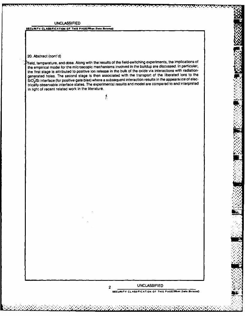
20. Abstract (cont'd)
ield, temperature, and dose. Along with the' results of the field-switching experiments, the implications ofthe empirical model for the microscopic mechanisms involved in the buildup are discussed. In particular,the first stage is attributed to positive ion release in the bulk of the oxide via interactions with radiation-
generated holes. The second stage is then associated with the transport of the liberated ions to the
SICO2/Si interface (for positive gate bias) where a subsequent interaction results in the appearaoce of elec-
trically observable interface states. The experimental results and model are compared to and interpretedin light of recent related work in the literature.
%" -,"
2 UNCLASSIFIED
SECURITY CLASSIFICATION OF TIS PAGEnbO Does Rnte.ed)
* **U ~UU~ . . . . . .. . . . . . . . . , .,.. .,*... ... ---.. % *%~* ~~*** .*--~*~.-:--\~:--;- ~* -- * :---.............................

CONTENTS
Page
1. INTRODUCTION ........................................................... 5
2. SAMPLES AND MEASUREMENT TECHNIQUES ......................... 5
3. EXPERIMENTAL RESULTS ................o............................... ... 6
'4. DISCUSSION .............................................................10
4.1 Review of Empirical Model .........................................114.2 Implications for Physical Mechanisms ..............................12'4.3 Relation to Other Work ............................................15
5. CONCLUSIONS ............................................................19
ACKNOWLEDGEMENTS ...........................................................19
LITERATURE CITED ...........................................................20
DISTRIBUTION ...............................................................23
FIGURES
1. Oxide field switching experiment .......................................
2. Effect of switching gate-bias polarity on interface states ............ 9
3. Effect of switching gate-bias polarity and magnitude on
interface states ......................................................10
TABLE
1. Effect of Gate-Bias Polarity on Buildup of InterfaceStates, Nit ........................................................... 9
Accezio Fo
NTf9 CRA&IDTIC TABGrnamouicedo
u.4.0
... .... .... .... .. ..
-... - . .... ...........
A00~ h ai &$Paol
3 m
Az_

1. INTRODUCTION
The generation of radiation-induced interface states has been reported formany years in the literature.1 -
4 Our group has previously reported work, inwhich we observed a time-dependent buildup of interface states, taking placeover several thousand seconds, in metal-oxide-semiconductor (MOS) capacitorsunder positive bias following pulsed electron-beam irradiation. We initiallyexamined the buildup in several key experiments by varying the magnitude ofthe field across the oxide at critical times during the period of interface-state generation. 2 The results of these experiments indicated that two sepa-rate stages were required to describe the buildup of interface states in thesestructures.5s* The first stage, which occurs on the time scale of the trans-port of radiation-generated holes through the oxide or to the SiO 2 /Si inter-face, determines the final or saturation value of interface states and wasfound to be field dependent and temperature independent. The second stage,which begins after the hole transport and continues for several thousand sec-onds, determines the time scale for the buildup and was found to be dependenton both field and temperature.
In this report, we further examine the buildup in several experiments byvarying both the polarity and magnitude of the field across the oxide duringthe two stages of the buildup. Both early (10-6 to 1 s) and late (I to 104 s)time regimes are explored, and the results are interpreted in terms of theirimplications for physical processes occurring during the two stages of thebuildup. In particular, the first stage is identified as the interaction ofradiation-generated holes in the bulk of the oxide that leads to the releaseof positive ions (possibly H+). The second stage is then associated with thetransport of the liberated ions to the Si0 2 /Si interface, where a subsequentinteraction results in the appearance of electrically observable interfacestates.
2. SAMPLES AND MEASUREMENT TECHNIQUES
The MOS capacitors used in these experiments were supplied by Hughes Air-craft Corporation and consisted of 96.5-nm wet-grown SiO 2 on nominal 3 to 5 Q-cm <100> n-type Si. The wet oxide was grown at 950 C in pyrogenic H2 0 andannealed in N2 for 20 min; Al electrodes were vapor-deposited from a carbon
IP. S. Winokur, J. M. McGarrity, and H. E. Boesch, Jr., IEEE Trans. Nucl. Sci. NS-23 (1976),1580.
2P. S. Winokur, H. E. Boesch, Jr., J. M. McGarrity, and F. B. McLean, J. Appl. Phys. 50
(1979), 3492.3T. P. Ma, G. Scoggan, and R. Leone, Appl. Phys. Lett. 27 (1975), 61.4C. T. Sah, IEEE Trans. Nucl. Sci. NS-23 (1976), 1563.H. E. Boesch, Jr., IEEE Trans. Nuc. Sd. NS-29 (1982), 1446.*The work reported in the present paper was observed for MOS capacitors that employed a thin
(<100 nm) SiO z layer with reduced hole trapping, i.e., radiation "hardened." Interface-statebuildup resulting from apparently different processes has been observed in MOS capacitors employ-
ing thicker (>100 nm) SiO 2 layers; see reference 5.
5 2
.4*.

. I-
crucible. An initial interface-state density at midgap of -6 x 1010 cm-2 V
was calculated from quasistatic capacitance-voltage (C-V) curves by the Berg-lund technique. 6 Bias-temperature stressing the capacitors at 200 C and 20 Vfor 5 min resulted in a flatband voltage shift of 70 mV. Voltage stressing atroom temperature and fields from 1 to 6 MV/cm under positive and negative bias
for 1 hr resulted in a flatband voltage shift of less than 100 mV and negli-gible interface-state production. For these capacitors, we concluded thatlateral charge nonuniformities at the Si0 2 /Si interface were small, becauseC-V traces taken at 77 K before and after irradiation had essentially the samedistortion.7
The buildup of interface states following irradiation was monitoredthrough several measurement techniques. In a very fast field-switching exper-iment, we measured C-V curves at 295 and 77 K using a C-V apparatus that ap-plied a 50-ms voltage ramp and monitored sample capacitance with a phase-sensitive detector operating at 1 MHz. The difference in the flatband voltagebetween these curves (i.e., the Gray-Brown shift, 8 VGB) yields an integratedvalue of interface states over -0.25 eV of the Si band gap defined by theFermi levels at 295 and 77 K. In other field-switching experiments, we meas-ured C-V traces using a system employing a 1-MHz capacitance meter and a 10-sduration voltage ramp. These C-V traces were analyzed by the Terman tech-nique 9 to obtain a distribution of interface states over the Si band gap. Theresulting distribution of interface sta es was integrated from midgap to flat-band to provide single values, Nit (cm-), of interface states in the samples.
3. EXPERIMENTAL RESULTS
In one experiment, MOS capacitors were irradiated to -60 krad(Si0 2 ) with asingle 4-ps 13-MeV electron pulse from an electron linear accelerator (LINAC).During the radiation pulse, the sample was maintained under positive bias cor-responding to a 1-MV/cm electric field across the oxide layer. At a predeter-mined time following the radiation pulse, tsw, the field was switched to
5 MV/cm. (A switch takes less than 1 us.) The field was then maintained for-2000 s, at which time a Gray-Brown measurement was performed to determine theincrease in radiation-induced interface states. This field switching is shownschematically in figure la.
The measured increase in the Gray-Brown shift from its preirradiationvalue, AVGB, is plotted in figure lb for switching times of 1 ps, 160 ps, 10ms, and 1 s. The upper and lower horizontal lines in the figure correspond tomeasured increases in the Gray-Brown shift for cases in which the oxide fieldwas held constant (not switched during and after the radiation pulse) at 5 and1 MV/cm, respectively. As reported previously, the final or saturation valueof interface states is strongly field dependent and increases with increasing
C. N. Berglund, IEEE Trans. Electron Devices ED-13 (1966), 701.7C. C. Chang and W. C. Johnson, IEEE Trans. Electron Devices ED-24 (1977), 1249.8P. V. Gray and 0. M. Brown, Appl. Phys. Lett. 8 (1966), 31.
9L. M. Terman, Sol. St. Electron. 5 (1962), 285.
6

-.~~~-- L_ 1 .-- . -- 3
(a)
Figure 1. Oxide field switching
experiment: (a) oxide field as a
function of time following a 4-psj
*. LINAC irradiation. At a predeter-10- 0.- W 10-2 100 mined time, tsw, oxide field is
switched from 1 to 5 MV/cm. Hole
TiUSls) transport regime is shown to cover
Item transportfgime times out to 1 s. (b) Measured in-
crease in Gray-Brown shift, AVGB, %
(b) plotted for switching times of
AvO at 5E ,/r 1 us, 160 jis, 10 ms, and 1 s
1.5 (circles). Upper and lower
horizontal lines correspond to
LIEAC, Skrad, measured increases in AVGB, where
wet aside oxide field is held constant (not
switched) at 5 and 1 MV/cm, respec-
S1.0- / ' tively. Dashed line is a calcula-
tion of expected increase in AVGBshltbased on based on details of hole transport.helm transport "-.
0.5"
0.05
106 10-4 10-2 10-
field.'0 It is evident that the value of the measured increases in the Gray-
Brown shift decreases uniformly from its constant 5-MV/cm value (-1.5 V) to
its constant 1-MV/cm value (-0.25 V) as tsw is increased. This corresponds tor- a decrease in the production of radiation-induced interface states as tsw is
increased. - -
P. S. Winokur. H. E. Boesch, Jr., J. M. McGarrtty, and F. B. McLean, IEEE Trans. Nucl. Sci .
NS-24 (1977). 2113.
2.
I-,-" . ' - -- '. , . . ... . - .., -.-:_, . " . .- - ... . . - . _

Several conclusions can be drawn from this experiment. First, the magni-tude of the applied field during the radiation pulse has essentially no effecton the final number of interface states. Clearly, the AVGB produced for aswitch from 1 to 5 MV/cm at 1 Ws after the radiation pulse is approximatelythe same as that for the case of a constant 5 MV/cm maintained both during andafter the radiation pulse. The small (5-percent) difference in the final num-ber of states can be easily explained by the slightly lower yield of electron-
hole pairs for a 1-MV/cm compared to 5-MV/cm irradiation."1 Second, radia-tion-generated electrons are not responsible for the buildup of the interfacestates. Electrons are swept out of the oxide during the radiation pulse (inpicoseconds) and are not affected by postirradiation bias switches. Sincethese bias switches have been shown to determine the magnitude of the finalinterface-state buildup, electrons cannot play a major role. On the otherhand, because of their relatively slow transport in Si0 2,1
2 most of theradiation-generated holes are present in the oxide at I Vs after the radiationpulse, and Lheir transport will be affected by postirradiation bias switches.This correlation is strengthened by a calculation of the final AVGB based onthe details of the hole transport; the result of this calculation is shown asthe dashed line in figure lb. In this calculation, AVGB is determined byweighting the Gray-Brown shifts for constant I- and 5-MV/cm irradiations(given by the horizontal lines) wittL the fraction of the hole transport atthose fields as predicted by the continuous time random walk (CTRW) model forhole transport in Si02 .12-
1 5 The agreement between calculated and measured
values of AVGB is seen to be good.
We performed another series of experiments to examine whether the interac-tion of holes which produces the interface states occurs at the Si0 2 /Si inter-face or in the Si0 2 bulk. In these experiments, we programmed the fast C-Vsystem to change the polarity of the applied bias at selected times after aseries of 5 to 7 LINAC pulses, delivered at the rate of 60/s, to obtain atotal dose of 600 to 800 krad(Si0 2 ) while avoiding problems of space chargeand heating.
In figure 2, we examine the effect of gate-bias polarity on the interface-state buildup. Curve A shows the buildup of interface states, Nit, under aconstant positive field of 4 MV/cm following a 600-krad(SiO2 ) LINAC irradia-tion. The buildup is seen to take place over several thousand seconds, whichis on a time scale considerably longer than the time it takes radiation-generated holes to transport to the Si0 2 /Si interface (milliseconds at4 My/cm).'s The final or saturation value of interface states is -3 x 1011cm For curve B, the holes were transported under negative bias to the Al/SiO 2 interface, and the bias was then switched positive at 0.8 s. For this
llH. E. Boesch, Jr., and J. M. McGarrity, IEEE Trans. Nucl. Sci. NS-23 (1976), 1520.12F. B. McLean, H. E. Boesch, Jr., and J. M. McGarrity, IEEE Trans. Nucl. Sci. NS-23 (1976),
1506.F. B. McLean and G. A. Ausman, Jr., Phys. Rev. B 15 (1977), 1052.
F. B. McLean, G. A. Ausman, Jr., H. E. Boesch, Jr., and J. M. McGarrity, J. Appl. Phys. 47(1976), 1529.
15 F. B. McLean, H. E. Boesch, Jr., and J. M. McGarrity, Proc. Intl. Conf. Physics of SiO2 and
Its Interfaces, Pergamon Press, New York (1978), p 19.
8

0 0AFigure 2. Effect of- LAC, 600 ki B switching gate-bias polarity-We OXk - on interface states, Nit , as -
a function of time for wet-oxide MOS capacitors
r- 2.0 - following a 600-krad(SiO 2 )IE LINAC irradiation. Curve 5
..,C A: oxide field is a constant
(not switched) +4 MV/cm.Curve B: oxide field
1.0 - switched from -4 to +4 MV/cm0 at 0.8 s. Curve C: oxide
field switched from -4 to +4IMV/cm at 29 s. Curve D:
. E i oxide field switched from -40.0-----, I to +4 MV/cm at 200 s. Curve
Pf 10s 101 102 103 104 E: oxide field switched from
Time(s) -4 to +4 MV/cm at 2000 s.
case, an interface-state buildup at late times was observed with a magnitudecomparable to that observed for a constant 4-MV/cm irradiation, i.e., curveA. For curves C through E, the holes were once again transported to the gate,but the field was maintained negative for 29, 200, and 2000 s, respectively,before being switched back positive. Here one can see the inhibiting effectof raintaining negative bias on the eventual interface-state buildup. Thelonger the bias is maintained negative following the hole transport, thesmaller the final or saturation value of interface states that is observed.If the bias is maintained negative for -2000 s, then no measurable buildup ofinterface states is observed.
Curves A and B in figure 2 TABLE 1. EFFECT OF GATE-BIAS POLARITYclearly indicate that the inter- ON BUILDUP OF INTERFACE STATES, Nitaction of holes that produces inter-face states is in the bulk of the First stage Second stage Nit (cm-2 )oxide, since the same final value of (10-6 to 1 s) (1 to 104 s) buildup
interface states is observed whetherthe radiation-generated holes trans- + + yes
port to the Al/SiO2 or to the noSi/SiO 2 interface. Table 1 summa-rizes the results of several field- + - noswitching experiments in which theinterface-state buildup was moni- - + yestored following irradiation for allcombinations of first- and second-stage gate-bias polarity. It isclear that a necessary condition to observe an N.t buildup is that the fieldbe maintained positive during the second stage Cafter the hole transport isconplete).
9.-..
................................... . ".

---I - -- -
_ : : j _ _ , . j. _ . . . _ . _ . . + . . .. -, "..-.. ,-~-"- -
In figure 3 we examine the.effect of switching both gate-bias polarity and .magnitude during the first and second stages of the buildup. Curve A repre-sents a constant 4-MV/cm irradiation with a buildup of radiation-inducedinterface states similar to that shown in figure 2. In curve B, the field was-4 MV/cm during the radiation pulses and hole transport stage, and then
switched to a positive value of 2 MV/cm. Here we observe a buildup which isapproaching the same saturation value as for curve A, but at a reduced rate.This result is in agreement with work we have previously published 2 thatconcludes that the field during the first stage determines the final value ofinterface states, while the field during the second stage determines the timescale for the buildup. More specifically, as the field during the secondstage is reduced, the rate of buildup is reduced. In curve C, the field was-2 MV/cm during the radiation pulses and hole transport, and then switched to
a positive value of 4 MV/cm. For this case, we observe a lower final value ofinterface states at late times, but a buildup to saturation at the same rateas curve A, i.e., a 4-MV/cm irradiation. Once again this agrees with earlierwork 2 showing that the magnitude of the field during the hole transport orfirst stage determines the final value of interface states, while the field
during the second stage sets the rate of buildup.
LUACkfm,. Figure 3. Effect of
w Oxiswitching gate-bias
polarity and magnitudeI on interface states,
z.6 - Nit, as a function of- time in wet-oxide MOS
-a capacitors following a I-" 600-krad(SiO 2 ) LINAC.
irradiation. Curve1.0 - C A: oxide field is a
constant (not switched)+4 MV/cm. Curve B:oxide field switched
I.I ' from -4 to +2 MV/cm at
Powud is@ 184 , 0.8 s. Curve C: oxideUs (s) field switched from -2
to +4 MV/cm at 0.8 s.
4. DISCUSSION
Recently one of us (McLean) presented an empirical model of radiation-induced interface states in SiO 2 MOS capacitors.'' The formulation explicitlyaddressed the time-dependent two-stage nature of the buildup process, and itgave the mathematical dependencies of the previously observed experimentalbuildup on time, field, temperature, and dose. Here we first briefly review
2P. S. Winokur, H. E. Boesch, Jr., J. M. McGarrity, and F. B. McLean, J. Appl. Phys. 50(1979), 3492.
16F. B. McLean, IEEE Trans. NucI. Sci. NS-27 (1980), 1651.
10
.,,. .
- J,.-+- " :. " +- --" '- -.-_ - ." -u-._,,.'.." ._. .-" ' ,. ._ ..- .-' _-+ ., ,. .
,.: , - o . " ' ". .- . - . " '. - '. " -", - " " ".-- "- - . _' . - -. . . '- .
- - r '- - _ r r ~
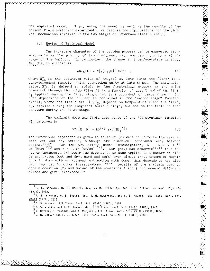
the empirical model. Then, using the macel as well as the results of thepresent fiela-switching experiments, we discuss the implications for the phys-ical mechanisms involved in the two stages of interface-state buildup.
4.1 Review of Empirical Model
The two-stage character of the buildup process can be expressed math-ematically as the product of two functions, each corresponding to a singlestage of the buildup. In particular, the change in interface-state density,
ANit(t), is written as
ANit(t) = NVt(EI,D)f(t/T) (1)
where Nlt is the saturated value of ANit(t) at long times and f(t/t) is atime-dependent function which approaches unity at late times. Tne saturatioT.value, N t, is determined solely by the first-stage process as the nrielt2-transport through the oxide film; it is a function of dose D and of the fiel'El applied during the first stage, but is independent of temperature. 2 Trhetime dependence of the buildup is contained in the "second-stage" functio,f(t/T), where the time scale T(T,E2) depends on temperature T and the fielo,E2 , applied during the long-term buildup stage, but not on the field or tem-perature during the first stage.
The explicit dose and field dependence of the "first-stage" function,It is given by 'a
NTt(E19D3 AD2/3 exp( EI/ 2 ) .2ii
The functional dependencies given in equation (2) were found to be the same inboth wet and dry oxides, although the numerical constants vary betweenoxides.'' For the wet oxides under investigation, A = 4 .6 - 1010cm-2Mrad -2 /3 and = 1.32 (MV/cm) 1 1 2 Our group has observed"' that th"rather unexpected 2/3 power law dependence on dose applies to a number of dif-ferent oxides (wet and dry, hard and soft) over almost three orders of magni-tude in dose with no apparent saturation with dose; this dependence has alsobeen reported by other investigators.1'8' 1 Details of the analysis used toobtain equation (2) and values of the constants A and 6 for several differentoxides are given elsewhere.-
P. S. Winokur, H. E. Boesch, Jr., J. M. McGarrity, and F. B. McLean, J. Appl. Phys. 50
(1979), 3492.10P. S. Winokur, H. E. Boesch, Jr., J. M. McGarrity, and F. B. McLean, IEEE Trans. Nucl. Sci.
NS-24 (1977), 2113.16 F. B. McLean, IEEE Trans. Nuci. Sci. NS-27 (1980), 1651.UP. S. Winokur and H. E. Boesch, Jr., IEEE Trans. Nucl. Sci. NS-27 (1980), 1647.18K. Naroke, M. Yoshida, and K. Maejuchi, IEEE Trans. Nucl. Sci. NS-30 (1983), 4054.
19C. M. Dozier and D. B. Brown, IEEE Trans. Nucl. Sci. NS-30 (1983), 4382.
p TII
,_,' .¢. . .'.. -'..'-,. - .,..•.'..'.-/...........".............. .. ,,....... ...... ...... .... . -.
- - ,. '.. - - - °.. . . .
Although for a fixed dose Nt is determined by the field during thefirst stage, ANit(t) does not achieve the saturation value until long timesafter the radiation pulse. At room temperature and for positive bias, theinterface states begin to be manifested typically from 0.1 to 1.0 s after thepulse and continue increasing in approximately logarithmic fashion until sat-uration occurs at thousands to tens of thousands of seconds. Hence, for pos-itive gate bias, Vg, the second-stage time-dependent function can be expressedapproximately as
f(t/t) ~ b ln(1 + t/) Vg > 0 , (3a)
for t less than the time at which saturation occurs, tsat . The factor b ischosen so that f(t/r) 1 1 as t 4 tsat , i.e., b = 1/ln(I + tsat/T). Fornegative bias
f(t/T) = 0 Vg < 0 . (3b)
The important quantity of interest associated with the second stageis the time scale T for the buildup; T was found to be both temperature andfield activated, i.e.,
= T0 exp(A/kT - aE2 ) ,()
where A is an activation energy, k is the Boltzmann constant, E2 is theapplied electric field during the second stage, and To and a are constants.From an analysis of the time-dependent data for the wet oxides as a functionof temperature and field A = 0.82 eV, a = 0.51 (MV/cm)- I, and the preexponential factor x. ; 2 x 10-13 s
4 .2 Implications for Physical Mechanisms
From the results of the field-switching experiments reported in thispaper, it is clear that the first stage of the radiation-induced interface-state buildup is associated with an interaction of the holes throughout thebulk of the oxide layer. To gain insight into the nature of the interaction,consider the field dependence of the first stage, i.e., of the saturatedinterface-state density (see eq (2)). The exponential dependence on the
* square root of the field is a classic signature of charge ejection over a* field-reduced Coulomb-like (1/r potential) barrier, i.e., the Schottky effect.
This would suggest as a possibility for the first-stage process an interactionof the holes in which some charged species is released. The fact that thefirst stage is temperature independent indicates that thermal energy is insig-nificant in the process; that is, essentially all the energy for bond breakingand charge release is derived from the transporting holes.
One envisions a process in which a hole makes a transition to alocalized trap site next to or involving a weakly bonded ion impurity, where
12....................................................................................... ...............................................................
.................... 1. .....................................

........ or le V N
the initial overall charge state of the impurity complex is neutral. In the
light of what is known about hole transport in SiO 2 ,'2-15 ' 20 ' 2 1 a broad dis-
tribution of energies with an average in the range from 0.5 to 1.0 eV isexpected to be deposited locally whenever a hole undergoes either a polaronhopping transition or a trapping event. (In a small fraction of transitions,such as for a long hop at high fields, the amount of energy transfer can besignificantly higher than the average.) The ion is then liberated by the sud-den localized energy excitation. If the released ion has positive charge (seebelow), then the interaction probably involves a charge-transfer process inwhich the hole is annihilated by an electron initially involved in bonding theion, and the positive charge is then carried by the ion. The defect site
remains in a neutral charge state.
With the first-stage process apparently being that of ion release inthe bulk, the interpretation of the long-term buildup stage becomes evident. J,It is simply that of a field-azz isted ionic transport to the interface with asubsequent interaction of the ions at the interface which produces the ob-served interface states. From table 1, the important polarity condition forit buildup is positive gate bias during the second, long-term buildup stage.
This then argues for a positively charged ion species, which would drifttoward the Si interface under positive bias. 5-A
Based on electrical measurements alone, we cannot identify the posi-tive ionic species or complex involved in the buildup process. Previously,"6
we have argued that the most likely candidate for the positive ion is H+ be-cause (I) hydrogen is present to some degree in all oxides, (2) the major dif-ference in the interface-state buildup in wet-grown versus dry-grown oxides issimply one of magnitude, with the buildup being considerably larger for wet-oxide capacitors,1 " (3) hydrogen is expected to be relatively mobile in SiO2at room temperature, and (4) H+ is known to be highly reactive at the SiO 2 /Siinterface. However, other positive ions such as Na+ or even ionic complexes(e.g., a mobile ion-defect complex) cannot be ruled out.
If the time scale is indeed related to a field-assisted thermally ac-tivated ionic transport process, then we argue that it should be possible toexpress equation (4) as
1= To exp[(A 0 - eaE/2)/kT] , (5)
12F. B. McLean, H. E. Boesch, Jr., and J. M. McGarrity, IEEE Trans. Nucl. Sci. NS-23 (1976).
1506.13F. B. McLean and G. A. Ausman, Jr., Phys. Rev. B 15 (1977). 1052.14F. B. McLean, G. A. Ausman, Jr., H. E. Boesch, Jr., and J. M. McGarrity, J. Appl. Phys. 47
1976), 152915F. B. McLean, H. E. Boesch, Jr., and J. M. McGarrity, Proc. Intl. Conf. Physics of Si02 and
Its Interfaces, Pergamon Press, New York (1978), p 19.16F. B. McLean, IEEE Trans. Nucl. Sci. NS-27 (1980), 1651.17P. S. Winokur and H. E. Boesch, Jr., IEEE Trans. Nucl. Sci. NS-27 (1980), 1647.21R.C. Hughes, Phys. Rev. B 15 (1977), 2012. %210. L. Curtis, Jr., and J. R. Srour, J. Appl. Phys. 48 (1977), 3819.
13
%. ... . . ...." -" " - '- . . . .- . ," - "" " " .- "-" •" " •, "•, - " •-••.-.".-.- -' - '.- , 4. ". "". .""" -" -"" . -N, .-.V",[

- . . . . . . . . . . . . . . .
- where A0 is the zero field activation energy for diffusion, a is an average"° hopping distance in the field direction, and a high field regime is assumed,
i.e., eaE/kT > 1. From the analysis of the field- and temperature-dependentdata, 1 6 we find an average hopping distance of 0.26 nm and zero field activa-tion energy of 0.87 eV. An average hopping distance of 0.26 nm is very rea-sonable. Indeed, this is precisely the average distance between nearest- Aneighbor oxygen atoms in amorphous SiO2 . One may well expect that H+ ionswould tend to temporarily bond to the lone-pair, nonbonding p orbitals on the0 atoms between hops and hence transport by hopping between nearby 0 atoms.We may also note that the preexponential factor that was determined for equa- 4%tion (4), t 0 2 x 10-13 s, is reasonable for ionic transport; it is about afactor of 10 larger than the period associated with the optical phonon vibra-tion in SiO 2 .
The approximate logarithmic buildup of Nit with time follows simplyfrom the dispersive nature of diffusive ionic transport, with the ions beingreleased throughout the SiO 2 bulk. The buildup is generally observed to occurover about three decades in time (see curves A of fig. 2 and 3). This spreadin time is directly correlated with the number of hops required for an ion totransit the entire film (-400), which corresponds to the saturation time forthe buildup, whereas the buildup begins at times comparable to a single hoptime for those ions released near the interface.
Because no tendency toward saturation with dose up to 20 Mrad(Si0 2 )was discernible in either hard wet or dry oxides,'' we are unable to estimatethe initial concentration of hydrogen in our SiO 2 films. Lower bounds on theconcentrations necessary to explain the experimental observations over thedose range studied were -1 x 10¹⁹ and -2 x 1018 cm- 3 in the wet and dryoxides, respectively. But these are lower bounds only; the actual concentra-tions may be significantly higher.
2 2
We may summarize at this point with the statement that much of theempirical information obtained from the electrical measurements of radiation-induced Nit can be understood simply on the basis of a positive ion release inthe bulk by hole transport and the subsequent field-induced drift of the ionsto the interface. In this light, the interpretation of the data in figures 2and 3 is rather straightforward. For curves A and B of figure 2, positiveions are released uniformly in the bulk during hole transport to either theSio 2 /Si or the Al/SiO2 interface. Immediately following the hole transport,
ions move under the applied positive field to the Si0 2 /Si interface where they -react to form interface states. In curves C through E, where the field iskept negative for increasingly long periods of time following the hole trans-port, a certain fraction of the released positive ions will be trapped or
16F. B. McLean, IEEE Trans. Nucl. Sc. NS-27 (1980), 1651.1 7P. S. Winokur and H. E. Boesch, Jr., IEEE Trans. Nucl. Sci. NS-27 (1980), 1647.
A. G. Revesz, IEEE Trans. Nucl. Sci. NS-24 (1977), 2102.
14.
...................................
% .
removed at the gate and cannot contribute to the eventual N buildup when thefield is returned positive. We therefore observe a lower final value of Nit_
the longer the field is maintained negative. Finally, if the field is main-tained negative for the time required for all the positive ions to transportto the gate (-2000 s, curve E), then no further Nit generation is observed
when the field is returned positive. A similar interpretation applies to thecurves of figure 3, with the additional points that (1) the final or saturatedvalue of Nit is determined by the field during the ion release process, i.e.,during the first-stage hole transport regime, and that (2) the field duringthe ion drift (second-stage) regime only affects the average drift velocity ofthe ions and therefore the time scale of the buildup.
When the ions reach the SiO 2 /Si interface, they undergo a furtherinteraction which results in the electrically observable interface states.Based on purely electrical measurements one cannot say anything specific aboutthe nature of the interaction at the interface. However, it would appear thatthis reaction occurs immediately. The time scale for the second stage as wellas the results of the bias-switching experiments can be entirely understood onthe basis of field-assisted ion diffusion, and there is no evidence of anysignificant time delay after the ions reach the interface before the appear- .ance of Nit. This is further indirect evidence that the positive ions in-volved are H , as they are expected to be highly reactive, whereas the resultsof bias-stress measurements on samples deliberately contaminated with alkaliions (Na+ , K+ ) indicate that these ions can be moved freely back and forthacross the oxide layer by reversing the bias polarity.
-41
4.3 Relation to Other Work -1
The role of a water-related species or defect in radiation-inducedinterface-state generation has been discussed by several authors. Sah4 in1976 proposed that the holes under positive gate bias interacted in the inter-face region to break weak Si-OH bonds, freeing OH radicals to drift towardthe gate, leaving behind dangling Si bonds which resulted in interface states.More recently Sah et al2 postulated that the Si dangling bonds are generatedby holes breaking weak Si-H bonds in the interface region. However, the two-stage character of the buildup cannot be understood with these processes,especially the long-term generation process which continues long after thehole transport is complete. In 1978, Svensson,2 in work based on previouswork of Revesz,2 2 postulated the essence of a possible two-stage process,namely, that transporting holes broke Si-H bonds in the bulk of the oxidefilm, leading to positively charged trivalent Si centers in the bulk and neu-tral interstitial hydrogen atoms which were free to diffuse away. Svensson
4C. T. Sah, IEEE Trans. Nucl. Sc. NS-23 (1976), 1563.22A. G. Revesz, IEEE Trans. Nucl. Sci NS-24 (1977), 2102.23C. T. Sah, J. Y. C. Sun, and J. J. T. Tzou, J. Appi. Phys. 54 (1983), 2547. ...24C. M. Svensson, Proc. Intl. Conf. Physics of StO 2 and Its-Interfaces, Pergamon Press, New
York (1978), p 328.
15 ..',.-'
.....--.-.. ,....
%''
then suggested that the atomic hydrogen which diffused to the interface re-
acted with Si-H bonds in the interface region to produce molecular hydrogen,H2 , and dangling Si bonds, which, as in the Sah model, resulted in the crea-tion of interface states.
Although this model does involve a two-stage process for the genera-tion of interface states, it fails to explain the field and polarity dependen-cies of the second stage. However, with the simple modification that H+ ionsreplace atomic hydrogen, the Svensson-Revesz model becomes entirely consistentwith the results of the present field-switching experiments. Further, thegeneration of Si dangling bonds upon irradiation and the correlation of thesedangling bond states with radiation-induced interface states have beeninferred from recent electron spin resonance measurements.
21
Recently, Grunthaner et a1 2 6 have also suggested a two-stage process- for radiation-generated interface states. Based on analysis of their x-ray
photoelectron spectroscopy (XPS) data, they postulate that the generation ofelectron-hole pairs in a strained region within about 3 nm of the Si0 2 /Si . .
. interface leads to rupture of strained Si-O bonds. In their model, the" dangling Si bonds remain immobile and can act as hole traps. However, the
nonbridging oxygen defects resulting from the bond rupture migrate toward theinterface because of the bond-strain gradient in the strained region. Thismigration is enhanced by the presence of OH groups. When the migration of thedefects is terminated at the Si02 /Si interface, dangling Si bonds are formed,resulting in interface states.
Although similar to our model in some respects, the Grunthaner modelis not consistent with our results on several accounts: (1) The migrating de-fect would have to be positively charged to account for the observed fielddependencies of the interface-state buildup. (2) The first-stage process inwhich holes release the positive-charge species is not restricted to the in-terface region, but occurs throughout the bulk of the oxide film. (This issupported by the data presented in fig. ib, which clearly show that theinterface-state buildup is related to the transport of holes and not to theelectron-hole pair-creation process itself. If the critical interaction ofthe holes occurred within a narrow region near the interface, then thereshould be a large difference in the magnitudes of the final saturated valuesof interface states between curves A and B in both fig. 2 and 3.) (3) Earlierwork on interface-state generation due to penetrating versus nonpenetratingradiation showed that it is not necessary for the ionizing radiation to pene-trate to the interface for interface states to be produced. 2 7
The presence of a strain region localized in the interface region ofthermally grown oxides, as inferred from the XPS studies, may be an importantfactor, however, in the interaction at the interface resulting in the observ-able interface states. In particular, the possible interactions may very well
25P. M. Lenahan and P. V. Dressendorfer, J. Appl. Phys. 54 (1983), 1457.F. J. Grunthaner, P. J. Grunthaner, and J. Maserjian, IEEE Trans. Nucl. Sc. NS-29 (1982) ,
1462.A27P. S. Winokur and M. M. Sokoloski, Appl. Phys. Lett. 28 (1976), 627.
16 ".'"4.." ,
%",'
-7 k 17 T - - .7 -. 7 -7
result in an increase in the localized strain fields at the interface. Oneindication that this may be the case is that a significant component of theradiation-induced interface-state distributions (in energy across the Si band-gap) is almost always observed to be U-shaped, with a relatively flat minimumnear midgap and a sharp rise toward the conduction and valence band edges.Recent density-of-state calculations for the SiO2 /Si system
2 8 indicate that aspecific defect in the interface region (such as a dangling Si bond) resultsin a peaked structure in the density-of-state distribution function, whichsharply contrasts with the universally observed U-shaped distributions. Thecalculations show, however, that fluctuations in bond angles and lengths inthe interface region can result in U-shaped distributions via band tailingfrom both the Si conduction and valence bands.
The most probable origin of such fluctuations is localized micro-scopic strain fields. In general, a certain amount of local reconstructionoccurs with the formation of any defect in Si0 2 , or even with a change in thecharge state of a defect due to the large lattice coupling with charge centersin SiO 2 (the polaron effect). As one example, there is well-documented elec-tron paramagnetic resonance (EPR) evidence 29 of a local reconstruction associ-ated with the formation of E' centers in vitreous SiO2 . Another possibleexplanation involves a class of defects, the so-called valence-alternationpairs, which are under increasingly active discussion'3-3 in the theory of
amorphous semiconductors, particularly the chalcogenide glasses, and have beendiscussed recently in connection with the nature of intrinsic defects invitreous SiO 2. 3 They provide a possible link between dangling Si bonds,appearing perhaps via interactions with H+ ions, as discussed above, and largelocalized strain fields. In any case, the possible role that strain plays ininterface-state generation deserves attention in future work.
The H + ion release/drift model for Nit generation proposed in thiswork is very similar to the process suggested by Feigl et al36 to account fortheir observations of oxide trapped charge and interface-state buildup uponelectron injection into thermal SiO 2 films.* They, too, envision a two-stageprocess, in which the first "fast" stage is attributed to an electron-inducedrelease of a mobile impurity species from an H/OH structural defect grown into
2R. B. Laughlin, J. 0. Joannopoulos, and D. J. Chadi, Proc. Intl. Conf. Physics of S102 andIts Interfaces, Pergamon Press, New York (1978), p 321.
29D. L. Griscom, Phys. Rev. 8 22 (1980), 4192.3P. W. Anderson, Phys. Rev. L-ett. 34 (1975), 953.R. A. Street and N. F. Mott, Phys.- Rev. Lett. 35 (1975), 1293.M. Kastner, 0. Adler, and H. Frltzsche, Phys. ev. Lett. 37 (1976), 1504. ., -
G. Lucovsky, Phil. Mag. B 39 (1979), 513; see also G. Lucovsky and 0. J. Chadi, Proc. Intl.Conf. Physics of MOS Insulators, Raleigh, Pergamon Press, New York (1980), p 301.34M. Pepper, IEEE Trans. Nucl. Sct. NS-25 (1978), 1283.
35C. T. White and K. L. Ngai, Proc. 6th Annual Conf. Physics of Compound Semiconductor Inter-faces, American Institute of Physics, New York (1979), p 1412.
36F. J. Feigl, 0. R. Young, 0. J. DiMaria, S. Lal, and J. Calise, J. Appl. Phys. 52 (1981),
5665.*The introduction rate of damage resulting from a hole flux is several orders of magnitude
greater than that from an equivalent avalanche-induced electron flux.
17
.,".-°-. .

the SiO2 network. They suggest neutral H as the most likely possibility for
the mobile impurity species. The second "slow" stage results from the trans-port of this species to the interface. They note that the detailed reactionsat the interface are not known. Except for the charge state of the mobile
species, this is the same scenario that is indicated by our data. It is con-ceivable that the charge state of the mobile species could be different in the
two cases because of the charge difference of the initiating carrier (elec-
trons as opposed to holes). This charge difference remains an open question.
In related work, 3' S. K. Lai suggests a two-step process for the gen-eration of interface states. In the first step, he simulates the effect of 1?radiation damage by the avalanche injection of holes from the Si into theSi0 2, where a certain percentage of holes are trapped in the Si0 2/Si interfaceregion. The second step involves the injection of electrons and their capture
by the trapped holes, and results in the generation of an interface-state dis-tribution with a peak in the Si band gap. The relationship betweer this workand our results is not clear at this time.
Finally, we note that the H+ ion release/drift model for Nit genera-tion is also compatible with results on interface-state generation under high-field stressing of MOS capacitors recently reported by Hu and Johnson.38 Uponpositive bias stressing at 90 K with fields of 7.1 to 7.5 MV/cm, they found abuildup of positive charge in the oxide layer, but they observe no buildup ofinterface states. Upon warming the samples to room temperature, however, theyobserved a time-dependent buildup of Nit, the number of which was correlatedwith the amount of positive charge initially present at 90 K after biasstressing. These results can be explained on the basis of H+ ions beingreleased in the bulk during the high-field stressing, either by field-injectedhot electrons or by holes generated as a result of impact ionization by thehot electrons moving under the high fields. But at 90 K the H+ ions areessentially immobile and remain near their points of origin. However, whenthe samples are warmed to room temperature the H+ become mobile, and thosewhich reach the Si0 2 /Si interface result in a time-dependent Nit buildup.
This is completely analogous to the manner in which the time-dependent buildupof radiation-induced Nit at room temperature was studied in the hard dry
oxide1 7 after irradiation at liquid nitrogen temperature.
17 P. S. Winokur and H. E. Boesch, Jr., IEEE Trans. Nuci. Sd. NS-27 (1980), 1647.37S. K. Lai, Appl. Phys. Lett. 39 (1981), 58.38G. Hu and W. C. Johnson, Appl. Phys. Lett. 36 (1980), 590.
18
* . .. . . . . . . . .. . . . .
*.° .o, - .• .. . .•, .. . . . . . . .• •.. . . . . '7 .
h•. ii5. CONCLUSIONS
In summary, it would appear that a large number of experimental observa- POFtions on the generation of interface states due to various stresses (holesfrom ionizing irradiation, injected electrons, high electric fields) can be
explained by a two-stage process. The first stage is the bulk release of amobile species due to the interaction of the stressing agent (holes, elec-
trons, high fields). The second "long-term" buildup stage is then associatedwith the drift of the released mobile species to the interface, where a subse-
quent reaction results in the observable interface states. It appears likelythat the mobile species is a water-related ion or defect. We have argued that
it is H' for the case of ionizing radiation.
ACKNOWLEDGEMENTS
The authors wish to thank J. M. McGarrity for helpful discussions andguidance, and T. Taylor for his assistance in some of the experiments.
19
i': • '°- °

LITERATURE CITED
1. P. S. Winokur, J. M. McGarrity, and H. E. Boesch, Jr., IEEE Trans. Mudl.
Sci. NS-23 (1976), 1580.
*2. P. S. Winokur, H. E. Boesch, Jr., J. M. McGarrity, and F. B. McLean, J.Appl. Phys. 50 (1979), 3492.
3. T. P. Ma, G. Scoggan, and R. Leone, Appi. Phys. Lett. 27 (1975), 61.
14. C. T. Sah, IEEE Trans. Nuci. Sci. NS-23 (1976), 1563.
5. H. E. Boesch, Jr., IEEE Trans. Nuel. Sci. NS-29 (1982), 1446.
6. C. N. Berglund, IEEE Trans. Electron Devices ED-13 (1966), 701.
7. C. C. Chang and W. C. Johnson, IEEE Trans. Electron Devices ED-24 (1977),12149.
8. P. V. Gray and D. M. Brown, Appi. Phys. Lett. 8 (1966), 31.
*9. L. M. Terman, Sol. St. Electron. 5 (1962), 285.
10. P. S. Winokur, H. E. Boesch, Jr., J. M. McGarrity, and F. B. McLean, IEEETrans. Nuci. Sdi. NS-24I (1977), 2113.
11. H. E. Boesch, Jr., and J. M. McGarrity, IEEE Trans. Nuci. Sci. NS-23(1976), 1520.
12. F. B. McLean, H. E. Boesch, Jr., and J. M. McGarrity, IEEE Trans. Nuci.
Sci. NS-23 (1976), 1506.
13. F. B. McLean and G. A. Ausman, Jr., Phys. Rev. B 15 (1977), 1052.
* 14. F. B. McLean, G. A. Ausman, Jr., H. E. Boesch, Jr. , and J. M. McGarrity,J. Appi. Phys. 47 (1976), 1529.
15. F. B. McLean, H. E. Boesch, Jr., and J. M. McGarrity, Proc. Intl. Conf.Physics of Si0 2 and Its Interfaces, Pergamon Press, New York (1978), p19.
16. F. B. McLean, IEEE Trans. Nuci. Sci. NS-27 (1980), 1651. .-
* 17. P. S. Winokur and H. E. Boesch, Jr., IEEE Trans. Nuci. Sci. NS-27 (1980), .-
16147.
18. K. Naroke, M. Yoshida, and K. Maejuchi, IEEE Trans. Nuci. Sci. NS-30(1983), 40514.
19. C. M. Dozier and D. B. Brown, IEEE Trans. Nucl. Sci. NS-30 (1983), 4382.
20

7;. -
LITERATURE CITED (cont'd) • .
20. R. C. Hughes, Phys. Rev. B 15 (1977), 2012.
21. 0. L. Curtis, Jr., and J. R. Srour, J. Appl. Phys. 48 (1977), 3819.
22. A. G. Revesz, IEEE Trans. Nucl. Sci. NS-24 (1977), 2102. .
23. C. T. Sah, J. Y. C. Sun, and J. J. T. Tzou, J. Appl. Phys. 54 (1983),2547.
24. C. M. Svensson, Proc. Intl. Conf. Physics of SiO2 and Its Interfaces,Pergamon Press, New York (1978), p 328. .
25. P. M. Lenahan and P. V. Dressendorfer, J. Appl. Phys. 54 (1983), 1457.
26. F. J. Grunthaner, P. J. Grunthaner, and J. Maserjian, IEEE Trans. Nucl.Sci. NS-29 (1982), 1462.
27. P. S. Winokur and M. M. Sokoloski, Appl. Phys. Lett. 28 (1976), 627.
28. R. B. Laughlin, J. D. Joannopoulos, and D. J. Chadi, Proc. Intl. Conf.Physics of SiO2 and Its Interfaces, Pergamon Press, New York (1978), p321.
29. D. L. Griscom, Phys. Rev. B 22 (1980), 4192.
30. P. W. Anderson, Phys. Rev. Lett. 34 (1975), 953.
31. R. A. Street and N. F. Mott, Phys. Rev. Lett. 35 (1975), 1293.
32. M. Kastner, D. Adler, and H. Fritzsche, Phys. Rev. Lett. 37 (1976), 1504.
33. G. Lucovsky, Phil. Mag. B 39 (1979), 513; see also G. Lucovsky and D. J.Chadi, Proc. Intl. Conf. Physics of MOS Insulators, Raleigh, PergamonPress, New York (1980), p 301.
34. M. Pepper, IEEE Trans. Nucl. Sci. NS-25 (1978), 1283.
35. C. T. White and K. L. Ngai, Proc. 6th Annual Conf. Physics of CompoundSemiconductor Interfaces, American Institute of Physics, New York (1979),p 1412.
36. F. J. Feigl, D. R. Young, D. J. DiMaria, S. Lai, and J. Calise, J. Appl.Phys. 52 (1981), 5665.
37. S. K. Lai, Appl. Phys. Lett. 39 (1981), 58.
38. G. Hu and W. C. Johnson, Appl. Phys. Lett. 36 (1980), 590.
21
.]."'.. " •i .- ;. ... . . . ..- r -. ." '."- . .. . . . . .... ,. . . . .." ."-'<. " .
DISTRIBUTION
ADMINISTRATOR COMMANDER
DEFENSE TECHNICAL INFORMATION CENTER US ARMY NUCLEAR & CHEMICAL AGENCYATTN DTIC-DDA (12 COPIES) ATTN MONA-NV, MAJ DOMASZEKCAMERON STATION, BUILDING 5 7500 BACKLICK RD, BLDG 2073ALEXANDRIA, VA 22304-6145 SPRINGFIELD, VA 22150
OFFICE OF DEPUTY CHIEF OF STAFF ARMY RESEARCH OFFICEFOR RES, DEV, & ACQ PO BOX 12211
ATTN DAMA-ARZ-D, RES PROGRAMS ATTN SLCRO, DR. M. STROSCIO, ELECTRONICS DIVWASHINGTON, DC 20310 RESEARCH TRIANGLE PARK, NC 27709
HQ DEFENSE NUCLEAR AGENCY NAVAL RESEARCH LABORATORYATTN COL R. BELLEM ATTN CODE 6682, D. B. BROWNATTN RAEV, L. M. COHN ATTN CODE 6680, C. M. DOZIERATTN RAEV, R. C. ZITTEL ATTN CODE 6816, H. HUGHES6801 TELEGRAPH RD ATTN CODE 6816, B. LAMBERTALEXANDRIA, VA 22305 ATTN CODE 6813, M. G. ANCONA
ATTN CODE 6813, N. S. SAKSDEFENSE NUCLEAR AGENCY ATTN CODE 6810, J. M. KILLIANYATTN T. D. STANLEY 4555 OVERLOOK AVE, SW6801 TELEGRAPH RD WASHINGTON, DC 20375ALEXANDRIA, VA 22310
NAVY SP & WARFARE ..
BMD ADVANCED TECHNOLOGY CTR ATTN D. 0. PATTERSONPO BOX 1500 2207 PAUL SPRING PKYATTN F. M. HOKE, JR ALEXANDRIA, VA 22308ATC-OHUNTSVILLE, AL 35807 NAVAL WEAPONS SUPPORT CTR
ATTN CODE 6054, T. D. ELLISBMDSCOM ATTN CODE 6054, D. W. EMILYBMDSC-LEH ATTN CODE 6054, Y. D. KIMPO BOX 1500 ATTN CODE 6054, D. G. PLATTETERATTN DE VOORHEES CRANE, IN 47522ATTN C. HARPER
HUNTSVILLE, AL 35807 NAVAL WEAPONS SUPPORT CTR
R2 BOX 1229 . .US ARMY ELECTRONICS TECHNOLOGY & DEVICES ATTN J. L. RAMSEY
LABORATORY ODON, IN 47562ATTN T. HUNTERATTN B. PFEFFER ROME AIR DEVELOPMENT CENTERATTN E. H. POINDEXTER, DEVICE PHYSICS RADC/ESR
& ANALYSIS BRANCH ATTN A. R. FREDERICKSONFT MONMOUTH, NJ 07703-5302 ATTN J. C. GARTH
HANSCOM AFB, MA 01731US ARMY ETDLATTN DELET-ED, B. PFEFFER AIR FORCE WEAPONS LABFT MONMOUTH, NJ 07703 ATTN R. J. MAIER
KIRTLAND AFBUS ARMY LABCOM ALBUQUERUQE, NM 87117ATTN DELET-IB-P, R. J. ZETOFT MONMOUTH, NJ 07738 JET PROPULSION LABORATORY
ATTN B. PRICECOMMANDER 1834-A S 5TH AV J.US ARMY MATERIEL COMMAND 83-122ATTN AMCCN-N, MR. BASSETT MONROVIA, CA 910165001 EISENHOWER AVEALEXANDRIA, VA 22333-0001
23
'-a
DISTRIBUTION (cont'd)
JET PROPULSION LABORATORY ARACORATTN F. L. BOUQUET ATTN L. PALKUTIATTN M. G. BUEHLER 1280 BROOKINGSATTN M. K. GAUTHIER SUNNYVALE, CA 94086ATTN D. K. NICHOLSATTN R. SCOTT ATT BELL LABORATORIESATTN J. A. ZOUTENDYK ATTN A. SABNIS4800 OAK GROVE DR 1247 S CEDAR CREST BLVDPASADENA, CA 91109 ALLENTOWN, PA 18103
NATIONAL BUREAU OF STANDARDS BOEING AEROSPACE CO -. %
ATTN K. F. GALLOWAY PO BOX 3999GAITHERSBURG, MD 20899 ATTN ITSU ARIMURA
ATTN R. S. CALDWELLNATIONAL SECURITY AGENCY ATTN A. H. JOHNSTONATTN P. E. DE VOY 2R-O0FT MEADE, MD 20755 SEATTLE, WA 98124-.7".
SANDIA NATIONAL LAB BOEINGPO BOX 5800 ATTN P. R. MEASELATTN DEPT 2120, W. R. DAWES, JR. 9510 NE 5THATTN DIV 2142, F. W. SEXTON BELLEVUE, WA 95004ATTN DIV 2144, P. V. DRESSENDORFERATTN DIV 2144, D. M. FLEETWOOD CEA (FRANCE)ATTN DIV 2144, A. OCHOA ATTN L. J. LUCATTN DIV 2144, J. R. SCHWANK CENTRE D'ETUDES DE BRUYERES-ATTN DIV 2144, P. S. WINOKUR (20 COPIES) LE-CHATEL PB 12ATTN DIV 2155, F. N. COPPAGE BRUYERS LE CTL 91680 FRANCEATTN DIV 2155, J. E. GOVERATTN DIV 2155, T. F. WROBEL CENTRAL RESEARCH LAB-HATACHIATTN DIV 2157, D. W. BUSHMIRE 1-280ALBUQTJERQUE, NM 87185 ATTN TAKAHIRO OKABE
TOKYO 185 JAPAN ". "NASA/GODDARD SPACE FLIGHT CTPATTN CODE 311, J. W. ADOLPHSEN COMPUTER SCIENCES CORPATTN CODE 313, V. DANCHENKO ATTN J. DAVIS -. '-'
GREENBELT, MD 20904 1400 SAN MATEO SEALBUQUERQUE, NM 87108
NASA/GODDARD SPACE FLIGHT CTRATTN CODE 600, E. G. STASSINOPOULOS COMSAT LABSGREENBELT, MD 20771 ATTN D. MEULENBERG -" -
22300 COMSAT DRNASA HEADQUARTERS CLARKSBURG, MD 20871ATTN MARTIN M. SOKOLOSKINASA HEADQUARTERS, DC 20546 FULMER RESEARCH LABS
ATTN A. HOLMES-SIEDLENATIONAL BUREAU OF STANDARDS STOKE POGESATTN T. J. RUSSELL SLOUGH BERKS SL2 4QD ENGLANDATTN N. D. WILKINBLDG 245/C-333 GENERAL ELECTRICGAITHERSBURG, MD 20862 PO BOX 8555
M/S M1211AEROSPACE CORP ATTN RONALD E. SCHMIDTATTN A. J. CARLAN ArTN D. M. TASCA4951 ROCK VALLEY RD PHILADELPHIA, PA 19101RANCHO PALOS VD, CA 90274
HAHN-MEITNER-INST BERLIN
ATTN D. F. BRAEUNINGGLIENICKER STRASSE 100BERLIN 39 1000 W GEF.4ANY
24
.~~~~ .. . .. .

DISTRIBUTION (cont'd)
HARRIS SEMICONDUCTOR JAYCORPO BOX 883 ATTN S. C. ROGERSM/S 51210 2811 WILSHIRE BLVDATTN B. LONG STE 690MELBOURNE, FL 32901 SANTA MONICA, CA 90403
HONEYWELL S & RC KAMAN SCIENCES CORP
ATTN R. BELT ATTN E. E. CONRAD17835 18TH CR 1911 JEFFERSON DAVIS HWYPLYMOUTH, MN 55447 SUITE 1200
ARLINGTON, VA 22202HONEYWELL INCATTN A. P. JOHNSON KAMAN TEMPO2600 RIDGEWAY PKWY ATTN B. A. ALFONTEMN17-2341 2560 HUNTINGTON AVEMINNEAPOLIS, MN 55413 SUITE 500
ALEXANDRIA, VA 22303 kHUGHES AIRCRAFT COATTN K. G. AUBUCHON LOCKHEED MISSILE & SPACE CTR6155 EL CAMINO REAL ATTN L. J. DRIESM/S 116 9543/202CARLSBAD, CA 92008 3251 HANOVER ST
PALO ALTO, CA 94304HUGHES AIRCRAFT COPO BOX 92919 MARTIN MARIETTA LABSATTN D. BINDER ATTN S. P. BUCHNERLOS ANGELES, CA 90009 1450 S ROLLING RD
BALTIMORE, MD 21227IBMATTN A. EDENFELD MISSION RESEARCH CORPATTN L. R. ROCKETT ATTN R. PEASE9500 GODWIN DR 1720 RANDOLPH RD SEBLDG 867/1B ALBUQUERQUE, NM 87106MANASSAS, VA 22110
MISSION RESEARCH CORPIRT CORP ATTN A. H. KALMAATTN T. A. MARTIN 4935 N 30TH ST1364 BEVERLY RD STE 101 COLORADO SPRINGS, CO 80919McLEAN, VA 22101
MISSION RESEARCH CORPIRT CORP ATTN V. A. J. VAN LINTATTN J. C. PICKEL 5434 RUFFIN RD101 S KRAEMER B1 SAN DIEGO, CA 92123SUITE 132PLACENTIA, CA 92670 MISSION RESEARCH CORP
ATTN E. A. BURKSIRT CORP 11 INDIAN HILL RDPO BOX 85317 WOBURN, MA 01801ATTN J. C. AZAREWICZATTN J. W. HARRITY MYERS & ASSOCIATESATTN J. M. WILKINFELD ATTN D. K. MYERSSAN DIEGO, CA 92138 16415 RUSTLING OAK
MORGAN HILL, CA 95037JAYCORPO BOX 85154 NATIONAL SEMICONDUCTORATTN R. E. LEADON ATTN F. C. JONESSAN DIEGO, CA 92138 112 BELHAVEN DR
LOS GATUS, CA 95030
25
. " . -. " .'."".. .v-',.-".-.. " .'-, ...- . .-. -'-. -':..'.- '* .... , .. ...... .'. .- """"*- " "* - . " . -"-.-*' -?'
:. "- . " -. "N". : " :. -. "..V. ..- - . .- .-. .-
DISTRIBUTION (cont'd)
- NORTHROP RESEARCH & TECH CTR TEXAS INSTRUMENTS* ATTN ZEF SCHANFIELD PO BOX 225621
ATTN J. R. SROUR M/S 944ATTN M. M. MORIWAKI ATTN W. E. BAILEY
ONE RESEARCH PARK DALLAS, TX 75265
0355/T60PALOS VERDES, CA 90274 TEXAS INSTRUMENTS
Po BOX 660246* RAYTHEON ATTN T. F. CHEEK
ATTN H. L. FLESCHER M/S 3145
528 BOSTON PORT RD DALLAS, TX 75042
1R13SUDBURY, MA 01776 TEXAS INSTRUMENTS INC
ATTN F. W. POBLENZ
RCA CORP 1923 DEEP VALLEY DRMOORESTOWN CORP CENTER RICHARDSON, TX 75080
ATTN J. S. PRIDEMOREATL BLDG UNITED TECHNOLOGIES CORP MOSTEK
MOORESTOWN, NJ 08057 ATTN J. P. MIZECARROLLTON, TX 75006
RCA LABORATORIESDAVID SARNOFF RSRCH CTR UNITED TECHNOLOGIES MICROCENTER
ATTN R. K. SMELTZER ATTN C. W. GWYN
PRINCETON, NJ 08540 1365 GARDEN OF THE GODS RD
COLORADO SPRINGS, CO 80907RCAATTN H. S. VELORIC TRW INCRT-202 ATTN DR A. A. WITTELES
SSTC 6908 VERDES RIDGE RD
SOMERVILLE, NJ 08876 PALOS VERDES, CA 9074
RESEARCH TRIANGLE INSTITUTE UNIVERSITY OF NEW MEXICOPO BOX 12194 DEPT EEEATTN M. SIMONS TAPY HALL -
RESEARCH TRI PK, NC 27709 ATTN D. A. NEAMAN
ALBUQUERQUE, NM 87131SCIENCE APPLCTNS INT'L CORPATTN M. A. HOPKINS NORTH CAROLINA STATE UNIV
2615 PACIFIC COAST HWY ATTN J. R. HAUSER
STE 300 432 DANIELS HALLHERMOSA BEACH, CA 90254 RALEIGH, NC 27695
SCIENCE APPLCTNS INT'L CORP NORTH CAROLINA STATE UNIV
ATTN R. L. FITZWILSON PO BOX 791110210 CAMPUS PT DR ECE
SAN DIEGO, CA 92121 ATTN S. E. DIEHL-NAGLE
RALEIGH, NC 27695SEMICONDUCTOR RESEARCH CORP
PC BOX 12053 PENNSYLVANIA STATE UNIV
ATTN D. H. PHILLIPS DEPT OF ENGINEERING4501 ALEXANDER DR STE 301 ATTN P. M. LANAHANRESEARCH TRIANGLE PARK, NC 27709 123 HAMMOND BLDG
UNIVERSITY PARK, PA 1680.)TELEDYNE BROWN ENGINEERING
ATTN H. A. HARDT YALE UNIVERSITY704 CORLETT DR DEPT OF ELECTRICAL ENGINEERM/S 47 PO BOX 2157 YALE STATION
HUNTSVILLE, AL 35802 ATTN T. P. MANEW HAVEN, CT 06520
26

7-7 VIC. T.p-"
DISTRIBUTION (cont'd)
G. F. DERBENWICKCONSULTANT1626 VICKERS DRCOLORADO SPRINGS, CO 80907
G. C. MESSENGERSELF-EMPLYD ENGNRNG CNSLTNT3111 BEL AIR DR #7FLAS VEGAS, NV 89109
US ARMY LABORATORY COMMANDATTN COMMANDER, AMSLC-CGATTN TECHNICAL DIRECTOR, AMSLC-TD
INSTALLATION SUPPORT ACTIVITYATTN DIRECTOR, SLCIS-DATTN RECORD COPY, SLCIS-IM-TSATTN LIBRARY, SLCIS-IM-TL (3 COPIES)ATTN LIBRARY, SLCIS-IM-TL (WOODBRIDGE)ATTN TECHNICAL REPORTS BRANCH, SLCIS-IM-TRATTN LEGAL OFFICE, SLCIS-CC
HARRY DIAMOND LABORATORIESATTN D/DIVISION DIRECTORSATTN DIVISION DIRECTOR, SLCHD-RTATTN CHIEF, SLCHD-NW-EATTN CHIEF, SLCHD-NW-EBATTN CHIEF, SLCHD-NW-ECATTN CHIEF, SLCHD-NW-EDATTN CHIEF, SLCHD-NW-EEATTN CHIEF, SLCHD-NW-RATTN CHIEF, SLCHD-NW-RAATTN CHIEF, SLCHD-NW-RCATTN CHIEF, SLCHD-NW-REATTN CHIEF, SLCHD-NW-RHATTN CHIEF, SLCHD-NW-RIH.eATTN CHIEF, SLCHD-NW-PATTN CHIEF, SLCHD-TTATTN K. W. BENNETT, SLCHD-NW-RCATTN B. J. ROD, SLCHD-NW-RCATTN T. V. BLOMQUIST, SLCHD-NW-RCATTN F. B. McLEAN, SLCHD-NW-RC (20 COPIES)ATTN H. E. BOESCH, SLCHD-NW-RC (20 COPIES)
2'
27