Active Cells: A Programming Model for Configurable...
52
CASE STUDY 4: CUSTOM DESIGNED MULTI- PROCESSOR SYSTEM Active Cells: A Programming Model for Configurable Multicore Systems 328
Transcript of Active Cells: A Programming Model for Configurable...

CASE STUDY 4: CUSTOM DESIGNED MULTI-PROCESSOR SYSTEM
Active Cells:
A Programming Model for Configurable Multicore Systems
328
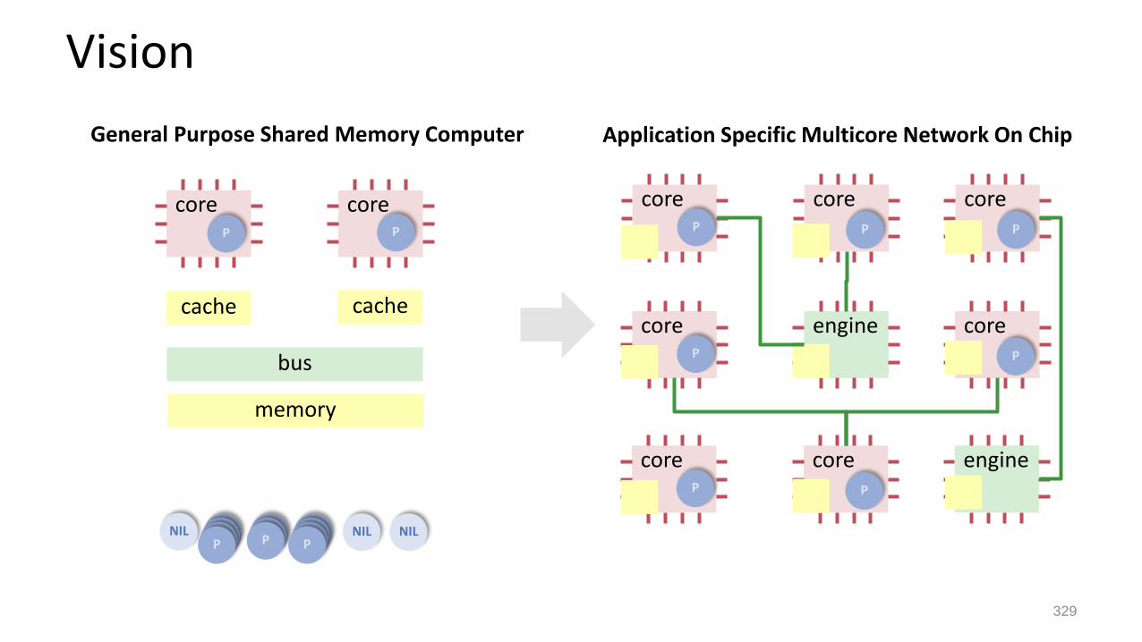
Vision
329
P P NILP NILNIL P P PP P PP P
core core
cache
bus
cache
memory
P P
core corePP
core engineP
core corePP
coreP
coreP
engine
General Purpose Shared Memory Computer Application Specific Multicore Network On Chip

Objectives
TRM Processor and Interconnects
Software Hardware Co-Design
The Active Cells Toolchain
Case Studies and Examples
330

Motivation: Multicore Systems Challenges
Cache Coherence
Shared Memory Communication Bottleneck
Thread Synchronization Overhead
Hard to predict performance of a program
Difficult to scale the design to massive multi-core architecture
331

Operating System Challenges
Processor Time Sharing
Interrupts
Context Switches
Thread Synchronisation
Memory Sharing
Inter-process: Paging
Intra-process, Inter-Thread: Monitors
332

Project Supercomputer in the PocketFunded by Microsoft in ICES programme, 2009 - 2014
Manycore architecture for embedded systems on the basis of programmable hardware (FPGA)
Emphasis on high-performance computing in the small in the field of sensor driven medical IT
Enhance industrial applications and ease teaching of parallel computing
333
Project Time
Generalpurposemanycorefor teaching
Processor Designs andInterconnects
Idea"Configurability over all levels"
Novel computing model and toolchain for constructing distributed system on chip.
ICES II

Focus: Streaming Applications
Structural Example: ECG for realtime desease detection
334

Stream Parallelism
Pipelining335
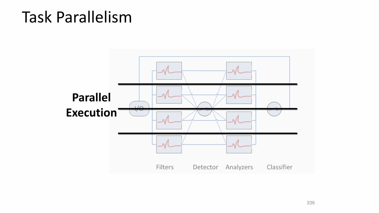
Task Parallelism
ParallelExecution
336

Data Parallelism
Vector ComputingLoop-level parallelism
337

Key Idea: On-chip distributed system
Replace shared memory by local memory
Message passing for interaction between processes
Separate processor for each process
Very simple processors
No scheduling, no interrupts,
Application-aware processors
Minimal operating system
Conceptually no memory bottleneck
Higher reliability and predictability by design
338338

4.1. HARDWARE BUILDING BLOCKSTRM AND INTERCONNECTS
339

TRM: Tiny Register Machine*
Extremely simple processor on FPGA with Harvard architecture.
Two-stage pipelined
Each TRM contains
Arithmetic-logic unit (ALU) and a shifter.
32-bit operands and results stored in a bank of 2*8 registers.
local data memory: d*512 words of 32 bits.
local program memory: i*1024 instructions with 18 bits.
7 general purpose registers
Register H for storing the high 32 bits of a product, and 4 conditional registers C, N, V, Z.
No caches
340* Invented and implemented by Dr. Ling Liu and Prof. Niklaus Wirth

TRM Machine Language
Machine language: binary representation of instructions
18-bit instructions
Three instruction types:
Type a: arithmetical and logical operations
Type b: load and store instructions
Type c: branch instructions (for jumping)
341
from Lectures on Reconfigurable Computing, Dr. Ling Liu, ETH Zürich

Encoding Overview Register Operations
Load and Store
Conditional Branches
Special Instructions
Branch and Link
342
091011131417
0 immRdop imm is zero extended to 32 bits
091011131417
1 RsRdop 0 0 0 x x 0
(a)
(b)
091011131417
1 VRsVRdop 1 0 0 x x x(c)
091011131417
1 x x xRdop 0 0 0 0 0 1(a)
(c)
091011131417
1 RsRdop 1 0 x x x x
091011131417
1 RsRdop 0 1 x x x x(d)
091011131417
1 x x xVRdop 1 0 0 001(b)
091011131417
1 RsRdop 101(e) xxxx
6
(a)
(b)
091011131417
0 RsRdop off
091011131417
1 RsVRdop off
3
3
off is zero extended to 13 bits
0910131417
cond1110 off off is sign extended to 12 bits0131417
1111 off off is 14-bit offset

TRM architecture
343
Figure from: Niklaus Wirth, Experiments in Computer System Design, Technical Report, August 2010
http://www.inf.ethz.ch/personal/wirth/Articles/FPGA-relatedWork/ComputerSystemDesign.pdf

Variants of TRM
FTRM
includes floating point unit
VTRM (Master Thesis Dan Tecu)
includes a vector processing unit
supports 8 x 8-word registers
available with / without FP unit
TRM with software-configurable instruction width (Master Thesis Stefan Koster,
2015)
344

First Experiment: TRM12A Multicore Processor Architecture on FPGA
345
Column 0
Column 1
Column 2
Column 3
H0
H1
H2H3
C0
inbound arbiteroutbound arbiter
inbound arbiteroutbound arbiter
inbound arbiteroutbound arbiter
inbound arbiter
outbound arbiter
N0
C7
N1
N2
C2
N6
N7
N8
C6
C1
C8
N3
N4
N5
N9
N10
N11
C5 C11
C4
C3
C10
C9
RS232TR
CiNi
: processor core : network controller RS232TR : RS232 transmitter receiver
Timer
LCD
LEDs
DDR2
•12 RISC Cores (two stage pipelined at 116MHz)
• Message passing architecture
•Bus based on-chip interconnect
• On-chip Memory controller
Ling Liu, A 12-Core-Processor Implementation on FPGA, ETH Technical Report, October 2009
ftp://ftp.inf.ethz.ch/pub/publications/tech-reports/6xx/646.pdf

Interface to network and I/O
TRM processor connected to a network controller („NetNode“)
TRM core 11 connected to RS232 controller, a 2-line LCD
controller, a timer and 8 LEDs
TRM processor core 6 connected to 512 MB DDR2 controller
Netnodes and RS232 controller treated as I/O port to the TRM
processor, communication with TRM core through 32-bit I/O bus
I/O accessed via memory mapped I/O at fixed addresses
346346
Problems with this approach
Not scalable
Huge resource consumption
Little but existing contention
347

Second Experiment: Ring of 12 TRMs
node0 node1 node2 node3 node4 node5
node11 node10 node9 node8 node7 node6
TRM0 TRM1 TRM2 TRM3 TRM4 TRM5
TRM11 TRM10 TRM9 TRM8 TRM7 TRM6
TR
MR
ing
RS232
TR
MR
ing
TR
MR
ing
TR
MR
ing
TR
MR
ing
TR
MR
ing
TR
MR
ing
TR
MR
ing
TR
MR
ing
TR
MR
ing
TR
MR
ing
TR
MR
ing
01111110
01111110
01111110
01111110
01111110
01111110
01111110
01111110
01111110 0111
111001111110
01111110
Slide from Dr. Ling Liu‘s Lecture Series on Reconfigurable Computing348

>trash
RingNode
RB SB
fromRing toRing
statuswreqinDataoutDatardreq
n-bit link
slot
receiving
sending
TRM
TRMRingChannel
ioadr outbus iord iowr inbus
dataToTRMdataFromTRM
dataFromRN statusOfRN
Slide from Dr. Ling Liu‘s Lecture Series on Reconfigurable Computing
Connection TRM / Ring
TRM
Adapter
Ring
• Ring interconnectvery simple
• Small router
• Predictable latency
349
Problems with this approach
Not scalable without huge loss of performance
Large delays
350

4.2 ACTIVE CELLS
Programming Model
Case Studies
351
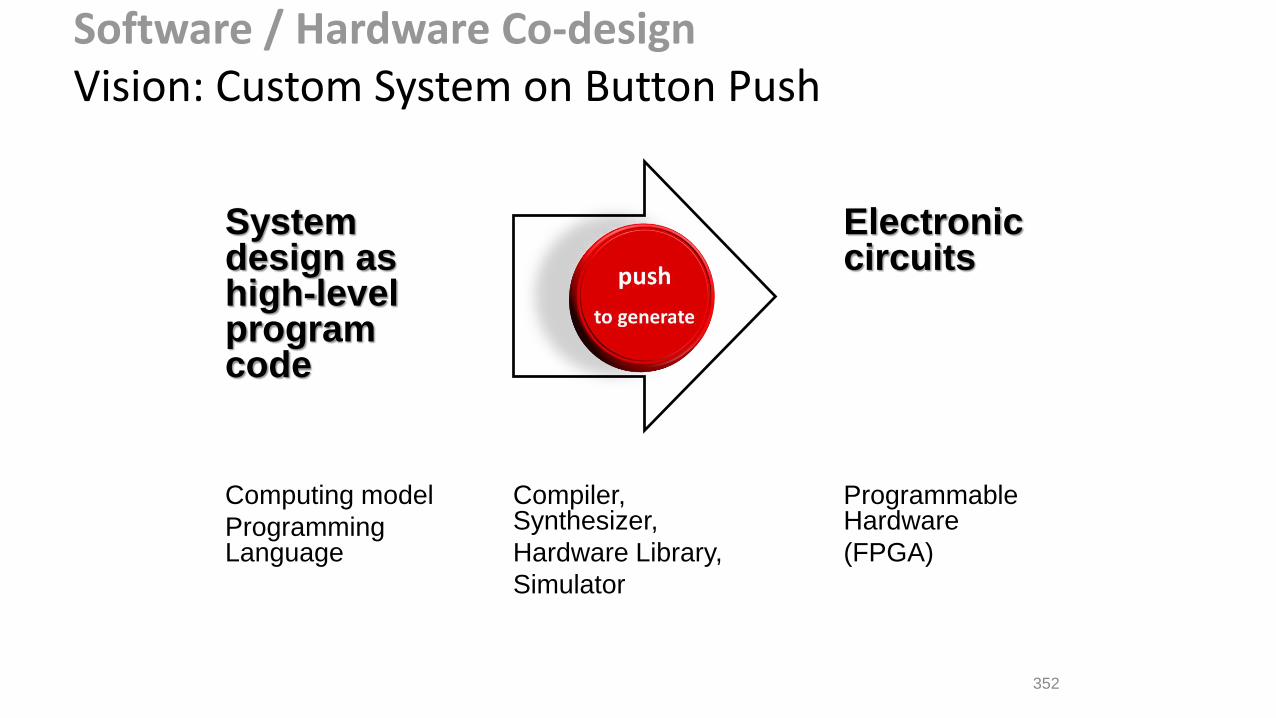
Software / Hardware Co-designVision: Custom System on Button Push
System design as high-level program code
Electronic circuits
Computing model
Programming Language
Compiler, Synthesizer,
Hardware Library,
Simulator
Programmable Hardware
(FPGA)
352

System specification, HW/SW partitioning
Program microcontroller in
C/C++
Programsystem specific
hardware in HDL
Compilation Synthesis
Microcontroller + machine code + specific hardware (eg. DSP)
Traditional HW/SW co-design for embedded
systems
Traditional HW/SW co-design
One Program
One Toolchain
System on FPGA
Active Cells approach for embedded systems
development
Goal
353

Software Hardware Map
channel
cell
fifo
354
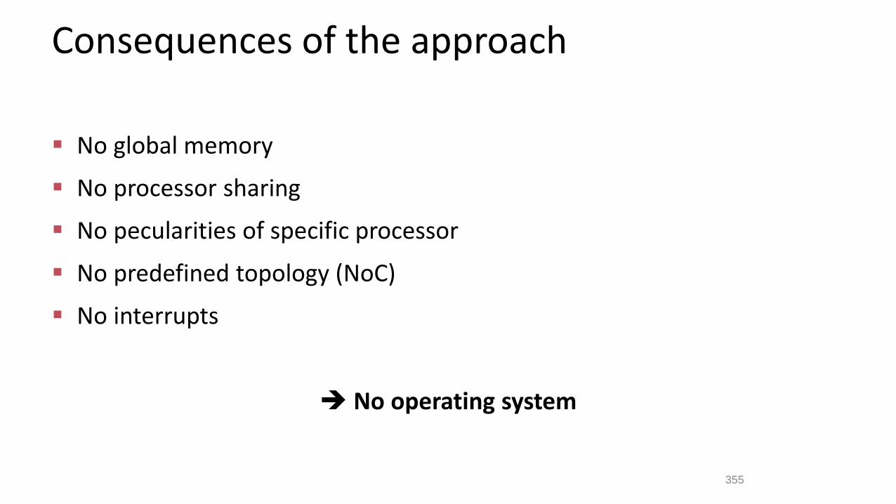
Consequences of the approach
No global memory
No processor sharing
No pecularities of specific processor
No predefined topology (NoC)
No interrupts
No operating system
355

Active Cells Computing Model
Distributed system in the small
Computation units: "Cells"
Different parallelism levels addressed by
Communication Structure (Pipelining, Parallel Execution)
Cell Capabilities (Vector Computing, Simultaneous Execution)
Inspired by
Kahn Process Networks
Dataflow Programming
CSP
..
356

Active Cell Components
Active Cell
Object with private state space
Integrated control thread(s)
Connected via channels
Cell Net
Network of communication cells
357
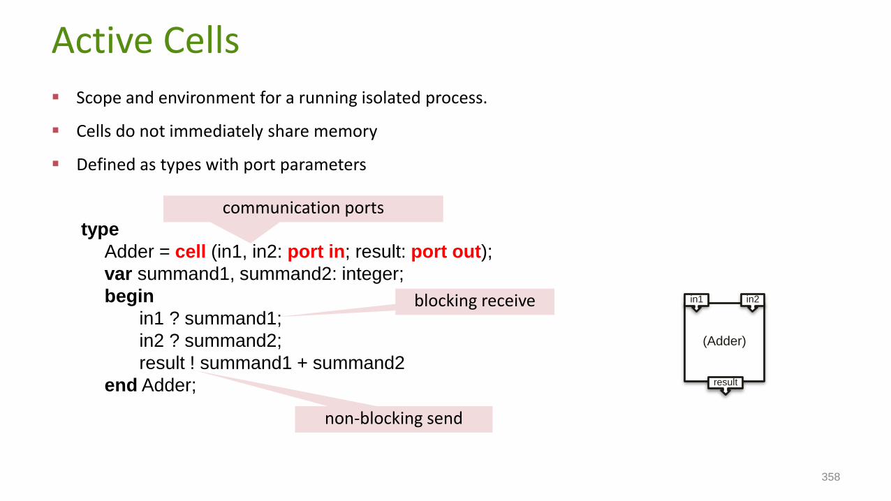
Active Cells Scope and environment for a running isolated process.
Cells do not immediately share memory
Defined as types with port parameters
358
type
Adder = cell (in1, in2: port in; result: port out);
var summand1, summand2: integer;
begin
in1 ? summand1;
in2 ? summand2;
result ! summand1 + summand2
end Adder;
communication ports
blocking receive
non-blocking send
(Adder)
result
in1 in2

Cell Constructors
Constructors to parameterize cells during allocation time
359
type
Filter = cell (in: port in; result: port out);
var ...; filterLength: integer;
procedure & Init(filterLength: integer)
begin self.filterLength := filterLength
end Init;
begin
(* ... filter action ... *)
end Filter;
var filter: Filter;begin
.... new(filter, 32); (* initialization parameter filterlength = 32 *)
constructor

Further Configurations:Cell Capabilities
Cells can be parametrized further, being provided with further capabilities or non-default values.
type
Filter = cell {Vector, DataMemory(2048), DDR2} (in: port in (64); result: port out);
var ...
begin
(* ... filter action ... *)
end Filter;
....
Cell is a VectorTRM with 2k of Data Memory and has access to DDR2 memory
This port is implemented with a (bit-)width of 64
360

Engine Cell Made From Hardware Special cells are provided as prefabricated hardware components (Engines).
361
type
Convolver2d= cell {Engine} (in: port in (64); result: port out);
end Convolver2d;

Hierarchic Composition: Cell Nets Cellnets consist of a set of cells that can be connected over their ports.
Allocation of cells: new statement
Connection of cells: connect statement
Cellnets can provide ports, ports of cells can be delegated to the ports of the net
Delegation of cells: delegate statement
Terminal (or closed) Cellnets* can be deployed to hardware
362*i.e. Cellnets without ports

Terminal Cellnet Example
363
cellnet Example;
import RS232;
type
UserInterface = cell {RS232}(out1, out2: port out; in: port in)(*...*) end UserInterface;
Adder = cell(in1, in2: port in; out: port out)(* ... *) end Adder;
var interface: UserInterface; adder: Adder
begin
new(interface);
new(adder);
connect(interface.out1, adder.in1);
connect(interface.out2, adder.in2);
connect(adder.result, interface.in);
end Example.
adder
(Adder)
result
in1 in2
interface
(UserInterface)
out1 out2
in
RS232

Hierarchic Composition Example
364
module SimpleCells
import RS232;
type
Adder = cell (in1, in2: port in; result: port out)(* ... *) end Adder;
Multiplier = cell (in1, in2: port in; result: port out)(* ... *) end Adder;
ScalarProduct*= cellnet (vx,vy,xw,xy: port in; result: port out)
var adder: Adder; multiplier1, multiplier2: Multiplier;
begin
new(mul1); new(mul2); new(adder);
delegate(vx, mul.in1); delegate(wx, mul1.in2);
delegate(vy, mul2.in1); delegate(wy, mul2.in2);
connect(mul1.result, adder.in1); connect(mul2.result, adder.in2);
delegate(result, adder.result)
end ScalarProduct;
end SimpleCells
port delegation
port delegation

Example of a wired Cellnetcellnet Test;
import SimpleCells, RS232;
type
Norm*=cellnet (vX,vY: port in; result: port out)
type
Dup*=cell(in: port in; out1,out2: port out)
var val: LONGINT;
begin
loop in ? val; out1 ! val; out2 ! val end
end Dup;
var s: SimpleCells.ScalarProduct2d; dup1, dup2: Dup;
begin
new(s); new(dup1); new (dup2);
connect (dup1.out1,s.vX); connect(dup1.out2,s.wX);
connect(dup2.out1,s.vY); connect(dup2.out2,s.wY);
delegate(vX,dup1.in);delegate(vY,dup2.in);
delegate(result,s.result);
end Norm;
s
(SimpleCells.ScalarProduct)
dup1
(Norm.Dup)
dup2
(Norm.Dup)
in
out1 out2
in
out1 out2
vX wx vY wY
result
norm(Norm)vX vY
result
365

Flattening
Calculator*=cell {RS232} (in: port in; outX,outY: port out)
var result: longint; vX,vY,wX,wY: longint;begin
loopRS232.ReceiveInteger(vX); RS232.ReceiveInteger(vY);send (outX,vX); send(outY,vY);receive (in,result);RS232.SendInteger(result);
end;end Calculator;
var calculator: Calculator; norm:Norm;begin
new(calculator); new(norm);connect(calculator.outX,norm.vX);connect(calculator.outY,norm.vY);connect(norm.result,calculator.in);
end Test.
s
(SimpleCells.ScalarProduct)
dup1
(Norm.Dup)
dup2
(Norm.Dup)
in
out1 out2
in
out1 out2
vX wx vY wY
result
norm(Norm)vX vY
result
calculator(Calculator)
in
outYoutX
norm.s.adder
(Adder)
result
in1 in2
norm.s.mul1
(Multiplier)
result
in1 in2
norm.s.mul2
(Multiplier)
result
in1 in2
norm.dup1
(Norm.Dup)
norm.dup2
(Norm.Dup)
in
out1 out2
in
out1 out2
calculator(Calculator)
in
outYoutX
RS232
Core1
Core2 Core3
Core4
Core6
Core5
366

Hybrid Compilation
Code body Role Compilation method
Cell (Softcore) Program logic Software Compilation
Cell (Engine) Computation unit Hardware Generation
Cell Net Architecture Hardware Compilation
367
cellnet N;
type A=cell(pi: port in; po: port out);var x: integer;begin… pi ? x; … po ! x; …end A;
var a,b: A;begin… connect(a.po, b.pi)end N.
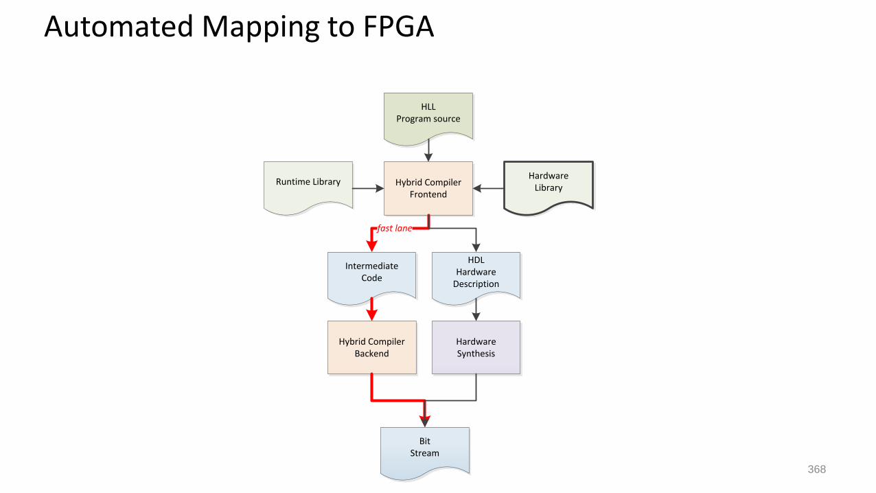
Automated Mapping to FPGA
368
HLLProgram source
Hybrid CompilerFrontend
IntermediateCode
HDLHardware
Description
Runtime LibraryHardware
Library
fast lane
BitStream
Hybrid CompilerBackend
HardwareSynthesis

Hardware Library
Computation Components
• General purpose minimal machine: TRM, FTRM
• Vector machine: VTRM
• MAC, Filters etc.
Communication Components
• FIFOs
• 32 * 128
• 512 * 128
• 32, 64, 128, 1k * 32
Storage Components
• DDR2 controller
• configurable BRAMs
• CF controller
I/O Components
• UART controller
• LCD, LED controller
• SPI, I2C controller
• VGA, DVI controller
369

TRM1
TRM2
TRM9
TRM10 TRM11 TRM12
FIFO1
FIFO8
FIFO9
FIFO16
FIFO17 FIFO18
FIFO19
FIFO20
FIFO33
FIFO34
UART
controller CF
controller
LCD
controller
Virtex-5LX50T FPGA
Xilinx ML505 board
RS232
CF
LCD
ECG
Sensor
·
·
·
·
·
·
Case Study 1: ECGFocus: Resources and Power
Real-time
ECG MonitorSignalinput
Wave proc_1
QRSdetect
HRV analysis
Disease classifier
Wave proc_2
Wave proc_8
ECG
bitstream
out
stream
370

Resources
ECG Monitor*
Maximum number of TRMs in communication chain
371
#TRMs #LUTs #BRAMs #DSPs TRM load
12 13859(48%)
52(86%)
12(25%)
<5%@116 MHz
FPGA #TRMs #LUTs #BRAMs #DSPs
Virtex-5 30 27692 (96%) 60 (100%)
30 (62%)
Virtex 6 500
*8 physical channels @ 500 Hz sampling frequency
implemented on Virtex 5 371

Comparative Power Usage
Preconfigured FPGA (#TRMs, IM/DM, I/O, Interconnect fixed)versus fully configurable FPGA (Active Cells)
System StaticPower (W)
Dynamic Power (W)
Preconfigured("TRM12")
3.44 0.59
Dynamicallyconfigured
0.5 0.58
86% saving!
Core 0
Core 1
Core 2
Core 3
Core 4
Core 5
Core 6
Core 7
Core 8
Core 9
Core 10
Core 11
Signal
inpu
t
Wave
proc_
1
QRS
det
ect
HRV analysis
Disease classifier
Wave
proc_2
Wave
proc_8
372

Case Study 2: Non-Invasive Continuous Blood Pressure MonitorFocus: Development Cycle Time
A2 Host OS with GUI on PCSensor control and medical algorithms on Spartan 6 FPGA
Sensors and Motorson Bracelet
ProjectResults
373

Medical Monitor Network On Chip
Dominated by TRM processors. Feedback driven.
374374
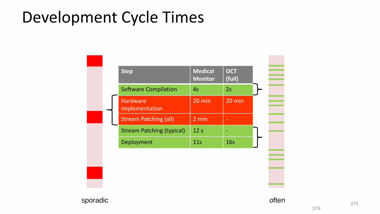
Development Cycle Times
Step Medical Monitor
OCT (full)
Software Compilation 4s 2s
Hardware Implementation
20 min 20 min
Stream Patching (all) 2 min -
Stream Patching (typical) 12 s -
Deployment 11s 16s
sporadic often375
375

Case Study 3: Optical Coherence TomographyFocus: Performance
A(λi) = A(1/fi)
f(z)
z-Axis Processing
1. Non uniform sampling
A(λi) A(f i)
2. Dispersion compensation
3. (Inverse) FFT
… for many lines x in a row (2d)
… and many rows y in a column (3d)
~
zx
y 376 376

A component of OCT image processingDispersion Compensation
Dominated by Engines. Dataflow driven.
377
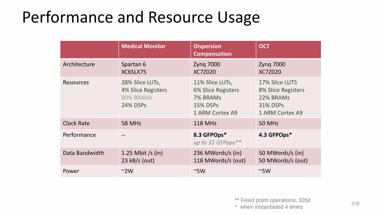
Performance and Resource Usage
Medical Monitor DispersionCompensation
OCT
Architecture Spartan 6XC6SLX75
Zynq 7000XC7Z020
Zynq 7000XC7Z020
Resources 28% Slice LUTs, 4% Slice Registers80% BRAMs24% DSPs
11% Slice LUTs, 6% Slice Registers7% BRAMs15% DSPs1 ARM Cortex A9
17% Slice LUTS8% Slice Registers22% BRAMs31% DSPs1 ARM Cortex A9
Clock Rate 58 MHz 118 MHz 50 MHz
Performance -- 8.3 GFPOps*up to 32 GFPops**
4.3 GFPOps*
Data Bandwidth 1.25 Mbit /s (in)23 kB/s (out)
236 MWords/s (in)118 MWords/s (out)
50 MWords/s (in)50 MWords/s (out)
Power ~2W ~5W ~5W
** Fixed point operations, 32bit
* when instantiated 4 times378
Conclusion
ActiveCells: Computing model and tool-chain for emerging configurablecomputing
Configurable interconnect Simple Computing, Power Saving
Hybrid compilation Decreased Time to Market
Embedding of task engines High Performance
379