ACQ400-MTCA-RTM-2 Functional Specification · PDF fileACQ400-MTCA-RTM-2 Functional...
24
ACQ400-MTCA-RTM-2 Functional Specification D-TACQ Solutions Ltd ACQ400-MTCA-RTM-2 Functional Specification High Performance Simultaneous Data Acquisition Rev 6 Page 1 of 24 Date: 14 January 2016
Transcript of ACQ400-MTCA-RTM-2 Functional Specification · PDF fileACQ400-MTCA-RTM-2 Functional...

ACQ400-MTCA-RTM-2 Functional Specification D-TACQ Solutions Ltd
ACQ400-MTCA-RTM-2 Functional Specification
High Performance Simultaneous Data Acquisition
Rev 6 Page 1 of 24 Date: 14 January 2016

ACQ400-MTCA-RTM-2 Functional Specification D-TACQ Solutions Ltd
Document Revisions
Rev Date Notes Author
1 11 Mar, 2015 Initial Release Peter Johnston
2 24 Mar, 2015 Clarifications on power sequencing [amended4.2.1.1.1], single-ended signals [added 3.2], table updates [5], provision for I2C testing [3.4.1, RP30 pins B7, B8, D7, F7] and possible +VADJ supply via AMC [3.4.2, pins D4, D5, D6].
Peter Johnston
3 7 Apr, 2015 Added electrical specification for I2C pins [3.4.1, RP30 pins B7, B8, D7, F7], updated I2C description [4.2] and clarified trace length matching [3.3].
Peter Johnston
4 5 Nov, 2015 Updated for Rev B. Changed management I2C devices [4.1] and removed a section on I2C recommendations [4.2] to match the board. Added Rev A section [7] for reference for previous board versions. Amended the SignallingLevels and Front Panel Clock sections [3.2, 4.3] to reflect Rev B changes.
Peter Johnston
5 12 Nov, 2015 Added note regarding D1.1 DESY Zone 3 Recommendation support. [3.4.3]
Peter Johnston
6 14 Jan, 2016 Added Drawing 2 showing Analogue Power Selection Switch location.
Peter Johnston
Rev 6 Page 2 of 24 Date: 14 January 2016

ACQ400-MTCA-RTM-2 Functional Specification D-TACQ Solutions Ltd
Table of Contents 1 Overview........................................................................................................4
1.1 Applications............................................................................................4 1.2 Overview.................................................................................................4 1.3 Glossary..................................................................................................5 1.4 Applicable Specifications.......................................................................5
2 Functionality...................................................................................................6 2.1 µRTM Compliance..................................................................................6 2.2 Appearance............................................................................................6
3 Interface Specification...................................................................................7 3.1 Zone 3 Connectors.................................................................................7 3.2 Zone 3 Signalling Levels........................................................................7 3.3 Zone 3 Trace Length Matching..............................................................7 3.4 Zone 3 Connector Pinout.......................................................................7
3.4.1 RP30...............................................................................................7 3.4.2 RP31.............................................................................................10 3.4.3 D1.1 DESY Zone 3 Recommendation Support............................13
4 Features.......................................................................................................14 4.1 µRTM Management I2C Bus................................................................14
4.1.1 EEPROM.......................................................................................14 4.1.2 Temperature Sensor.....................................................................14 4.1.3 LEDs and Hot Swap Handle GPIO Expander..............................14 4.1.4 Unique ID......................................................................................15
4.2 FPGA I2C Bus.......................................................................................15 4.2.1 FPGA I2C Bus Splitter...................................................................16
4.2.1.1 Splitter Arm 0.........................................................................16 4.2.1.2 Splitter Arm 1: ELF1..............................................................18 4.2.1.3 Splitter Arm 2: ELF2..............................................................19
4.3 Front-Panel Clock.................................................................................20 4.4 Voltage Rails........................................................................................20
4.4.1 Digital Power Supplies..................................................................20 4.4.2 Analogue Power Supplies.............................................................20 4.4.3 Analogue Voltage References.....................................................21
5 ACQ400-MTCA-RTM-2 Electrical Specification..........................................22 6 ACQ400-MTCA-RTM-2 Specification..........................................................23 7 ACQ400-MTCA-RTM-2 Rev A PCB............................................................24
7.1 LEDs and Hot Swap Handle GPIO Expander......................................24 7.2 Unique ID..............................................................................................24 7.3 Front Panel Clock.................................................................................24
Rev 6 Page 3 of 24 Date: 14 January 2016

ACQ400-MTCA-RTM-2 Functional Specification D-TACQ Solutions Ltd
1 Overview1. ACQ400-MTCA-RTM-2 is a MicroTCA MTCA.4 compliant, mid-size,
double-width µRTM module with sites for 2 x D-TACQ ELF modules.2. Sites for two full-size D-TACQ ELF modules, with ELF front panel on the
outward-facing edge of the µRTM.3. 2 x ADF-30 / ZD30 hard metric differential connectors to front side card.
◦ Pinout will be compliant with D1.0 DESY Zone 3 Recommendation (Rev A.3)
◦ Pinout allows connectivity with all D-TACQ ULPC and DLPC modules. Includes I2C interface to monitor ELF PROMS and control analogue and digital PSUs.
4. Includes analogue power supplies for ELF modules.
1.1 Applications
• Instrumentation applications, control and monitoring.
1.2 Overview
• Micro TCA [1.4] provides an instrument data acquisition platform with high bandwidth connections using fast serial buses, and standardised platform management using IPMI.
• Micro TCA Extensions for Physics [1.4] provides for a µRTM module that allows expansion for a processor card or adc module on the front side.
• The FMC standard [ 1.4.3] provides for low cost IO expansion to an FPGA processor module. D-TACQ provides a range of modules that extend this standard in two ways – the “ELF” [1.3] module, which more than doubles the payload of the module and the “ULPC” [1.3] and “DLPC” [1.3] pinouts that define a subset of IO's suitable for relatively low speed modules (up to 200MBytes/sec) and, in addition provide for analogue power rails from the baseboard. D-TACQ designs and markets a range of FMC and ELF modules, where the ELF modules in particular enable both high channel density and high analogue quality in the module.
• This document defines a MTCA.4 compliant µRTM that can act as a carrier for 2 x ELF modules. The µRTM is dependent on a suitable front side AMC module, similar to DAMC-FMC20.
Rev 6 Page 4 of 24 Date: 14 January 2016

ACQ400-MTCA-RTM-2 Functional Specification D-TACQ Solutions Ltd
1.3 Glossary
FMC: VITA57 FPGA Mezzanine Card
Xilinx ZYNQ System-on-chip
LPC: FMC Low pin count wiring standard
ELF: Superset variant of FMC (D-TACQ)
ULPC: FMC Ultra low pin count (D-TACQ)
DLPC: FMC Differential low pin count (D-TACQ)
SPL: Single Pin Lemo
MP: Management Power
1.4 Applicable Specifications
MTCA.0
AMC.0
MTCA.4
D1.0 DESY Zone 3 Recommendation (Rev A.3)
Management Interface IPMI v2.0
Rev 6 Page 5 of 24 Date: 14 January 2016
ACQ400-MTCA-RTM-2 Functional Specification D-TACQ Solutions Ltd
2 Functionality
2.1 µRTM Compliance
1. ACQ400-MTCA-RTM-2 is an MTCA.4 compliant, mid-size, double width µRTM module.
2. The ZONE 3 connector will be compatible with the DESY MTCA.4 D1.0 Zone 3 recommendation specification [1.4].
2.2 Appearance
Rev 6 Page 6 of 24 Date: 14 January 2016

ACQ400-MTCA-RTM-2 Functional Specification D-TACQ Solutions Ltd
3 Interface Specification
3.1 Zone 3 Connectors
ACQ400-MTCA-RTM-2 is fitted with connectors as specified by AMC.0 and MTCA.4. These are TE Connectivity 6469183-1 connectors.
Mating connectors for the AMC board should be compatible, for example the TE Connectivity 6469081-1 connectors.
3.2 Zone 3 Signalling Levels
JTAG and standard I2C lines operate at +3.3V logic levels.
Although the majority of ELF1 and ELF2 signals are routed as differential pairs, the ELF modules only use these as single-ended traces. The ELF modules do not use these as LVDS lines.
All ELF1 and ELF2 signal lines should be at +1.8V logic levels with the exception of dedicated ELF1/ELF2 I2C buses (if used). FPGA I2C should also be at +1.8V logic levels.
The front panel clock (output from RTM, input to AMC) is at LVDS signalling levels.
3.3 Zone 3 Trace Length Matching
On existing D-TACQ carriers, each bundle of signals going from the FPGA to each individual ELF site are length matched. For example, all ELF1 traces are matched, and all ELF2 traces are matched. We would recommend doing the same to an interfacing AMC board.
Length matching requirements are as follows:
• Length match signal pairs to within 0.254mm within each pair (P to N).
• Length match all ELF1 pairs to within 6.35mm pair-to-pair.
• Length match all ELF2 pairs to within 6.35mm pair-to-pair.
3.4 Zone 3 Connector Pinout
3.4.1 RP30
The RP30 connector conforms to the D1.0 DESY Zone 3 Recommendation.
All GND pins on RP30 are connected to Ground (GND or 0VD).
All ELF1 and ELF2 signal lines should be at +1.8V logic levels with the exception of dedicated I2C buses.
Route all ELFn_LAxxp/n signals as 100Ω differential pairs.
§ Some single-ended signals share pairs through the connector. Route ELFn signals as50Ω single-ended (not required for I2C) where marked.
Rev 6 Page 7 of 24 Date: 14 January 2016

ACQ400-MTCA-RTM-2 Functional Specification D-TACQ Solutions Ltd
# Typically used as clock lines depending on the module – route to clock-capable pinswhere marked if possible. If necessary, prioritise the pairs in the following order: CLK0 highest; CLK1, LA00 then LA01 lowest. Route as 100Ω differential pairs.
∑ Note we believe there is a small mistake in version A.3 of the D1.0 specification. MTCA.4 REQ 2-27 states for differential signal pairs, signals A, C and E shall be assigned as positive (+) and B, D and F as negative (-). However the pin names in Table 1 label both signals A/B and E/F as positive in some, but not all cases. We haveproceeded under the assumption that this was a typographical error but have noted where the ACQ400-MTCA-RTM-2 pin name differs.
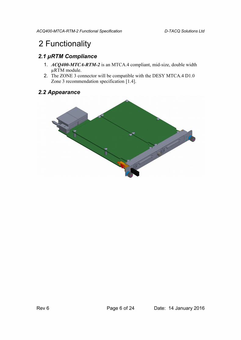
Pin Pin Name (DESYD1.0)
Function Name Description
A1 PWRA1 +12V µRTM-PWR Payload Power +12V
B1 PWRB1 +12V µRTM-PWR Payload Power +12V
A2 PWRA2 +12V µRTM-PWR Payload Power +12V
B2 PWRB2 +12V µRTM-PWR Payload Power +12V
A3 AMC_CLK1+ NC -
B3 AMC_CLK1- NC -
A4 AMC_TCLK+ NC -
B4 AMC_TCLK- NC -
A5 P30_IO+ / CC* ELF2_LA01_CCp #
B5 P30_IO- / CC* ELF2_LA01_CCn # ∑
A6 P30_IO+ / CC* ELF2_LA00_CCp #
B6 P30_IO- / CC* ELF2_LA00_CCn # ∑
A7 P30_IO+ ELF2_LA18_CCp
B7 P30_IO- Reserved (ELF2_SDA) ELF2 I2C Data, +3.3V Logic
A8 P30_IO+ ELF2_LA15p
B8 P30_IO- Reserved (ELF1_SCL) ELF1 I2C Clock, +3.3V Logic
A9 P30_IO+ / CC* ELF2_CLK0_M2Cp #
B9 P30_IO- / CC* ELF2_CLK0_M2Cn # ∑
A10 P30_IO+ / CC* ELF1_LA01_CCp #
B10 P30_IO- / CC* ELF1_LA01_CCn # ∑
C1 PS Present Present – connected to GND.
D1 SDA SDA I2C Data, +3.3V Logic
C2 MP +3V3_MP µRTM-MP Management Power +3V3
D2 SCL SCL I2C Clock, +3.3V Logic
C3 RTM_CLK1+ FP_CLK_p # Front Panel Clock, LVDS
D3 RTM_CLK1- FP_CLK_n # Front Panel Clock, LVDS
Rev 6 Page 8 of 24 Date: 14 January 2016
ACQ400-MTCA-RTM-2 Functional Specification D-TACQ Solutions Ltd
Pin Pin Name (DESYD1.0)
Function Name Description
C4 OUT0+ ELF1_CLK1_C2Mp # ELF1 Carrier to Mezzanine Clock
D4 OUT0- ELF1_CLK1_C2Mn # ELF1 Carrier to Mezzanine Clock
C5 P30_IO+ ELF2_LA23p §
D5 P30_IO- ELF2_LA22p §
C6 P30_IO+ ELF2_LA20p §
D6 P30_IO- I2C_SCL_1V8 § FPGA I2C Clock, +1.8V Logic [4.2]
C7 P30_IO+ ELF2_LA17_CCp
D7 P30_IO- Reserved (ELF2_SCL) ELF2 I2C Clock, +3.3V Logic
C8 P30_IO+ ELF2_LA14p
D8 P30_IO- NC -
C9 P30_IO+ ELF2_LA12p
D9 P30_IO- NC -
C10 P30_IO+ ELF2_LA10p
D10 P30_IO- ELF2_LA10n
E1 TCK AMC_TCK JTAG, +3.3V Logic
F1 TDO AMC_TDO/ELF1_TDI1 JTAG, +3.3V Logic
E2 TDI ELF2_TDO/AMC_TDI2 JTAG, +3.3V Logic
F2 TMS AMC_TMS JTAG, +3.3V Logic
E3 OUT2+ NC -
F3 OUT2- NC -
E4 OUT1+ ELF2_CLK1_C2Mp # ELF2 Carrier to Mezzanine Clock
F4 OUT1- ELF2_CLK1_C2Mn # ELF2 Carrier to Mezzanine Clock
E5 P30_IO+ ELF2_LA21p §
F5 P30_IO- I2C_SDA_1V8 § FPGA I2C Data, +1.8V Logic [4.2]
E6 P30_IO+ ELF2_LA19p §
F6 P30_IO- I2C_RESETn § Reset line for I2C Bus Splitter, +1.8V Logic [4.2.1]
E7 P30_IO+ / CC ELF2_LA16p
1 Assuming this direction. This can be swapped on the ACQ400-MTCA-RTM-2 via a jumper if incorrect. There was no data regardingthe direction of this pin.2 As above.
Rev 6 Page 9 of 24 Date: 14 January 2016

ACQ400-MTCA-RTM-2 Functional Specification D-TACQ Solutions Ltd
Pin Pin Name (DESYD1.0)
Function Name Description
F7 P30_IO- / CC Reserved (ELF1_SDA) ∑ ELF1 I2C Data, +3.3V Logic
E8 P30_IO+ / CC ELF2_LA13p
F8 P30_IO- / CC NC - ∑
E9 P30_IO+ ELF2_LA11p
F9 P30_IO- ELF2_LA11n
E10 P30_IO+ ELF2_LA09p
F10 P30_IO- ELF2_LA09n
3.4.2 RP31
The RP31 connector conforms to the D1.0 DESY Zone 3 Recommendation.
All GND pins on RP30 are connected to Ground (GND or 0VD).
All ELF1 and ELF2 signal lines should be at +1.8V logic levels with the exception of dedicated I2C buses.
Route all ELFn_LAxxp/n signals as 100Ω differential pairs.
§ Some single-ended signals share pairs through the connector. Route ELFn signals as50Ω single-ended (not required for I2C) where marked.
# Typically used as clock lines depending on the module – route to clock-capable pinswhere marked if possible. If necessary, prioritise the pairs in the following order: CLK0 highest; CLK1, LA00 then LA01 lowest. Route as 100Ω differential pairs.
∑ Note we believe there is a small mistake in version A.3 of the D1.0 specification. MTCA.4 REQ 2-27 states for differential signal pairs, signals A, C and E shall be assigned as positive (+) and B, D and F as negative (-). However the pin names in Table 1 label both signals A/B and E/F as positive in some, but not all cases. We haveproceeded under the assumption that this was a typographical error but have noted where the ACQ400-MTCA-RTM-2 pin name differs.
β The pinout of the Zone 3 connectors is fully compatible with the DESY D1.0 specification as it stands, however we believe there is a potential hole in the specification in that there could be an FPGA I/O voltage mismatch between the AMC board and the μRTM and ELF cards. Currently the required +1.8V would be generatedseparately by both front and rear cards. We would recommend the AMC card providesthis +1.8V (at a maximum current of 300mA) to the μRTM to power the I/O supplies of any ELF modules. This is similar to the way an FMC/ELF card receives its “+VFMCIO” voltage from the carrier. If implementation is desired, spare pins which could potentially be used for this supply voltage are marked with the β symbol. Some customers may have these lines connected by default. D-TACQ recommends connecting these lines via resistor jumpers to allow an AMC card to be fully DESY D1.0 compliant.
Rev 6 Page 10 of 24 Date: 14 January 2016

ACQ400-MTCA-RTM-2 Functional Specification D-TACQ Solutions Ltd
Pin Pin Name(DESY D1.0)
Function Description D1.1[3.4.3]
A1 P31_IO+ ELF2_LA08p
B1 P31_IO- ELF2_LA08n
A2 P31_IO+ ELF2_LA05p
B2 P31_IO- ELF2_LA05n
A3 P31_IO+ / CC ELF2_LA02p
B3 P31_IO- / CC ELF2_LA02n ∑
A4 P31_IO+ / CC ELF1_LA20p
B4 P31_IO- / CC NC - ∑
A5 P31_IO+ ELF1_LA17_CCp
B5 P31_IO- NC -
A6 P31_IO+ ELF1_LA14p
B6 P31_IO- NC -
A7 P31_IO+ / CC* ELF1_LA00_CCp #
B7 P31_IO- / CC* ELF1_LA00_CCn #
A8 P31_IO+ / CC* ELF1_CLK0_M2Cp #
B8 P31_IO- / CC* ELF1_CLK0_M2Cn #
A9 P31_IO+ ELF1_LA07p Ø
B9 P31_IO- ELF1_LA07n Ø
A10 P31_IO+ ELF1_LA04p Ø
B10 P31_IO- ELF1_LA04n Ø
C1 P31_IO+ ELF2_LA07p
D1 P31_IO- ELF2_LA07n
C2 P31_IO+ ELF2_LA04p
D2 P31_IO- ELF2_LA04n
C3 P31_IO+ ELF1_LA23p §
D3 P31_IO- ELF1_LA22p §
C4 P31_IO+ ELF1_LA19p
D4 P31_IO- NC (+VADJ) β Not Connected via Jumper site – Provision for supplying +VADJ from AMC if required.
C5 P31_IO+ ELF1_LA16p
D5 P31_IO- NC (+VADJ) β Not Connected via Jumper site – Provision for supplying +VADJ from AMC if required.
C6 P31_IO+ ELF1_LA13p
D6 P31_IO- NC (+VADJ) β Not Connected via Jumper site
Rev 6 Page 11 of 24 Date: 14 January 2016

ACQ400-MTCA-RTM-2 Functional Specification D-TACQ Solutions Ltd
Pin Pin Name(DESY D1.0)
Function Description D1.1[3.4.3]
– Provision for supplying +VADJ from AMC if required.
C7 P31_IO+ ELF1_LA11p
D7 P31_IO- ELF1_LA11n
C8 P31_IO+ ELF1_LA09p
D8 P31_IO- ELF1_LA09n
C9 P31_IO+ ELF1_LA06p Ø
D9 P31_IO- ELF1_LA06n Ø
C10 P31_IO+ ELF1_LA03p Ø
D10 P31_IO- ELF1_LA03n Ø
E1 P31_IO+ ELF2_LA06p
F1 P31_IO- ELF2_LA06n
E2 P31_IO+ ELF2_LA03p
F2 P31_IO- ELF2_LA03n
E3 P31_IO+ ELF1_LA21p
F3 P31_IO- NC -
E4 P31_IO+ ELF1_LA18_CCp
F4 P31_IO- NC -
E5 P31_IO+ / CC ELF1_LA15p
F5 P31_IO- / CC NC -
E6 P31_IO+ / CC ELF1_LA12p
F6 P31_IO- / CC NC -
E7 P31_IO+ ELF1_LA10p
F7 P31_IO- ELF1_LA10n
E8 P31_IO+ ELF1_LA08p
F8 P31_IO- ELF1_LA08n
E9 P31_IO+ ELF1_LA05p Ø
F9 P31_IO- ELF1_LA05n Ø
E10 P31_IO+ ELF1_LA02p Ø
F10 P31_IO- ELF1_LA02n Ø
Rev 6 Page 12 of 24 Date: 14 January 2016

ACQ400-MTCA-RTM-2 Functional Specification D-TACQ Solutions Ltd
3.4.3 D1.1 DESY Zone 3 Recommendation Support
Compared with the DESY D1.0 Zone 3 recommendation, the DESY D1.1 recommendation replaces 6 LVDS I/O signals for 2 high-speed links on the P31 connector. ACQ400-MTCA-RTM-2 is still compatible with this standard, but with reduced functionality: operation is limited to a single ELF site.
Please see the final column in the RP31 table [3.4.2] for affected pins marked with Ø.
This may affect customers who wish to use DESY's DAMC-FMC25 AMC.
Rev 6 Page 13 of 24 Date: 14 January 2016
ACQ400-MTCA-RTM-2 Functional Specification D-TACQ Solutions Ltd
4 Features
4.1 µRTM Management I2C Bus
ACQ400-MTCA-RTM-2 provides the standard management hardware as required by the MTCA.4 specification. These devices are all accessed via the standard I2C bus andare detailed as follows.
The µRTM Management I2C bus may be combined with other µRTM management devices [4.2.1.1] via 0Ω jumpers.
4.1.1 EEPROM
Device: M24C64
I2C Address: 0x50
A 64kbit (8Kbytes) EEPROM compatible with the MTCA.4 specification1 is providedto store FRU and other information. The EEPROM may be write-protected to prevent accidental overwrites via the LED and Hot Swap Handle GPIO Expander [4.1.3].
4.1.2 Temperature Sensor
Device: LM75
I2C Address: 0x48
A temperature sensor compatible with IPMI v2.0 [1.4] as called for by the MTCA.4 specification is provided to monitor the temperature of the analogue power supplies.
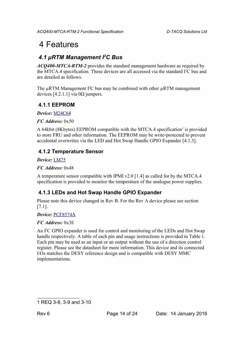
4.1.3 LEDs and Hot Swap Handle GPIO Expander
Please note this device changed in Rev B. For the Rev A device please see section [7.1].
Device: PCF8574A
I2C Address: 0x3E
An I2C GPIO expander is used for control and monitoring of the LEDs and Hot Swap handle respectively. A table of each pin and usage instructions is provided in Table 1. Each pin may be used as an input or an output without the use of a direction control register. Please see the datasheet for more information. This device and its connected I/Os matches the DESY reference design and is compatible with DESY MMC implementations.
1 REQ 3-8, 3-9 and 3-10
Rev 6 Page 14 of 24 Date: 14 January 2016
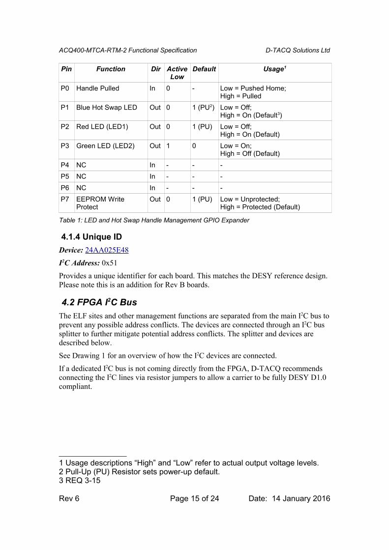
ACQ400-MTCA-RTM-2 Functional Specification D-TACQ Solutions Ltd
Pin Function Dir ActiveLow
Default Usage1
P0 Handle Pulled In 0 - Low = Pushed Home; High = Pulled
P1 Blue Hot Swap LED Out 0 1 (PU2) Low = Off;High = On (Default3)
P2 Red LED (LED1) Out 0 1 (PU) Low = Off; High = On (Default)
P3 Green LED (LED2) Out 1 0 Low = On; High = Off (Default)
P4 NC In - - -
P5 NC In - - -
P6 NC In - - -
P7 EEPROM Write Protect
Out 0 1 (PU) Low = Unprotected; High = Protected (Default)
Table 1: LED and Hot Swap Handle Management GPIO Expander
4.1.4 Unique ID
Device: 24AA025E48
I2C Address: 0x51
Provides a unique identifier for each board. This matches the DESY reference design. Please note this is an addition for Rev B boards.
4.2 FPGA I2C Bus
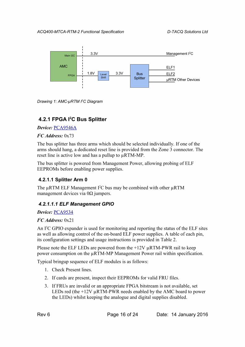
The ELF sites and other management functions are separated from the main I2C bus toprevent any possible address conflicts. The devices are connected through an I2C bus splitter to further mitigate potential address conflicts. The splitter and devices are described below.
See Drawing 1 for an overview of how the I2C devices are connected.
If a dedicated I2C bus is not coming directly from the FPGA, D-TACQ recommends connecting the I2C lines via resistor jumpers to allow a carrier to be fully DESY D1.0 compliant.
1 Usage descriptions “High” and “Low” refer to actual output voltage levels.2 Pull-Up (PU) Resistor sets power-up default.3 REQ 3-15
Rev 6 Page 15 of 24 Date: 14 January 2016
ACQ400-MTCA-RTM-2 Functional Specification D-TACQ Solutions Ltd
4.2.1 FPGA I2C Bus Splitter
Device: PCA9546A
I2C Address: 0x73
The bus splitter has three arms which should be selected individually. If one of the arms should hang, a dedicated reset line is provided from the Zone 3 connector. The reset line is active low and has a pullup to µRTM-MP.
The bus splitter is powered from Management Power, allowing probing of ELF EEPROMs before enabling power supplies.
4.2.1.1 Splitter Arm 0
The µRTM ELF Management I2C bus may be combined with other µRTM management devices via 0Ω jumpers.
4.2.1.1.1 ELF Management GPIO
Device: PCA9534
I2C Address: 0x21
An I2C GPIO expander is used for monitoring and reporting the status of the ELF sitesas well as allowing control of the on-board ELF power supplies. A table of each pin, its configuration settings and usage instructions is provided in Table 2.
Please note the ELF LEDs are powered from the +12V µRTM-PWR rail to keep power consumption on the µRTM-MP Management Power rail within specification.
Typical bringup sequence of ELF modules is as follows:
1. Check Present lines.
2. If cards are present, inspect their EEPROMs for valid FRU files.
3. If FRUs are invalid or an appropriate FPGA bitstream is not available, set LEDs red (the +12V µRTM-PWR needs enabled by the AMC board to power the LEDs) whilst keeping the analogue and digital supplies disabled.
Rev 6 Page 16 of 24 Date: 14 January 2016
Drawing 1: AMC-µRTM I2C Diagram

ACQ400-MTCA-RTM-2 Functional Specification D-TACQ Solutions Ltd
4. If FRUs are valid, and an appropriate FPGA bitstream is available, set LEDs green as appropriate, enable the analogue and digital power supplies (no sequencing is required for these), and load the appropriate bitstream.
If the FPGA I/O voltage (+1.8V) is provided to the µRTM via the AMC, this should be gated by the AMC in a similar way to µRTM-PWR (+12V) and µRTM-MP (+3.3V) and enabled at the same time as the digital supplies.
Pin Function Dir ActiveLow
Default Usage1
P0 ELF1 Green LED Out 0 0 Low = Off (Default); High = On
P1 ELF1 Red LED Out 0 0 Low = Off (Default); High = On
P2 ELF2 Green LED Out 0 0 Low = Off (Default); High = On
P3 ELF2 Red LED Out 0 0 Low = Off (Default); High = On
P4 ELF1 Present In 1 - Low = Present; High = Not Present
P5 ELF2 Present In 1 - Low = Present; High = Not Present
P6 Analogue Supplies Enable
Out 1 0 Low = Enable; High = Disable (Default)
P7 Digital Supplies Enable
Out 0 0 Low = Disable (Default); High = Enable
Table 2: ELF Management GPIO
4.2.1.1.2 ELF Power Supply Monitor 1
Device: AD7417
I2C Address: 0x28
Two devices are provided for monitoring the levels of the on-board power supplies. Each supply is divided down to an appropriate level to be monitored by the device so equations to convert the input in Volts back to the actual rail voltage are given inTable 3. The negative voltage rail uses the +3.3V rail as a reference, therefore the +3.3V rail on ELF Power Supply Monitor 2 [4.2.1.1.3] should be measured first.
The AD7417 also provides another temperature reading for the board.
1 Usage descriptions “High” and “Low” refer to actual output voltage levels.
Rev 6 Page 17 of 24 Date: 14 January 2016

ACQ400-MTCA-RTM-2 Functional Specification D-TACQ Solutions Ltd
Input Voltage Rail Input Conversion
1 -Vanalogue ((input_in_V * 33) – (measured_3.3V_rail_in_V * 28)) / 5
2 +Vanalogue input_in_V * 11
3 +5Vanalogue input_in_V * 4.012
4 +2.5Vref input_in_V * 2
Table 3: ELF Power Supply Monitor 1 Inputs
4.2.1.1.3 ELF Power Supply Monitor 2
Device: AD7417
I2C Address: 0x29
Two devices are provided for monitoring the levels of the on-board power supplies. Each supply is divided down to an appropriate level to be monitored by the device so equations to convert the input in Volts back to the actual rail voltage are given inTable 4. Use the +3.3V input value as a reference for the -Vanalogue measurement on ELF Power Supply Monitor 1 [4.2.1.1.2].
The AD7417 also provides another temperature reading for the board.
Input Voltage Rail Input Conversion
1 +2.5V input_in_V * 2
2 +3.3V input_in_V * 2
3 +1.8V input_in_V * 2
4 +5Vref input_in_V * 4.012
Table 4: ELF Power Supply Monitor 2 Inputs
4.2.1.2 Splitter Arm 1: ELF1
Each ELF module provides a FRU EEPROM holding card identifying information. Each ELF module also typically provides an AD7417 to monitor temperature and voltage rails.
The ELF1 site has its geographical address pins set as follows:
GA1:GA0 = 1:01
This means its AD7417 device (if present) and EEPROM will have addresses as givenbelow.
4.2.1.2.1 EEPROM
Device: M24C64
1 The ANSI/VITA 57.1 Specification flips the geographical address bits as they are connected to the address pins of I2C devices: Observation 5.22: GA[0] is connected to Address bit [1] and GA[1] is connected to Address bit [0].
Rev 6 Page 18 of 24 Date: 14 January 2016

ACQ400-MTCA-RTM-2 Functional Specification D-TACQ Solutions Ltd
I2C Address: 0x51
This contains FRU information such as card model, serial number, etc.
4.2.1.2.2 Power Supply Monitor
Device: AD7417
I2C Address: 0x29
The monitored voltages on these devices typically vary between modules due to their different supply requirements. Please contact D-TACQ for details of voltages and conversion equations for specific modules.
4.2.1.2.3 Other Devices
Some cards also have GPIO expanders providing extra functionality to a board such asgain control. Please contact D-TACQ for individual module requirements.
4.2.1.3 Splitter Arm 2: ELF2
Each ELF module provides a FRU EEPROM holding card identifying information. Each ELF module also typically provides an AD7417 to monitor temperature and voltage rails.
The ELF1 site has its geographical address pins set as follows:
GA1:GA0 = 0:11
This means its AD7417 device (if present) and EEPROM will have addresses as givenbelow.
4.2.1.3.1 EEPROM
Device: M24C64
I2C Address: 0x52
This contains FRU information such as card model, serial number, etc.
4.2.1.3.2 Power Supply Monitor
Device: AD7417
I2C Address: 0x2A
The monitored voltages on these devices typically vary between modules due to their different supply requirements. Please contact D-TACQ for details of voltages and conversion equations for specific modules.
1 The ANSI/VITA 57.1 Specification flips the geographical address bits as they are connected to the address pins of I2C devices: Observation 5.22: GA[0] is connected to Address bit [1] and GA[1] is connected to Address bit [0].
Rev 6 Page 19 of 24 Date: 14 January 2016

ACQ400-MTCA-RTM-2 Functional Specification D-TACQ Solutions Ltd
4.2.1.3.3 Other Devices
Some cards also have GPIO expanders providing extra functionality to a board such asgain control. Please contact D-TACQ for individual module requirements.
4.3 Front-Panel Clock
A LEMO 00-type connector is provided on the μRTM faceplate allowing an external signal to be applied. This may be used as either clock or trigger.
Input voltage range of the connector is standard TTL: 0 to +5V.
On Rev A boards, the incoming clock signal is converted to +1.8V logic and is output directly on the Zone 3 connectors.
On Rev B boards, the incoming clock signal is converted to an LVDS differential pair (matching the DESY D1.0 specification) and output on the Zone 3 connectors.
Due to the input containing an overvoltage clamp diode, the external clock input is only available if the digital supplies are enabled.
4.4 Voltage Rails
Each ELF module has different voltage and power requirements. The supplies on-board ACQ400-MTCA-RTM-2 provide enough power for every combination of module. No two ELF cards will require a current draw from the AMC module of morethan 3A, as defined by the MTCA.4 specification1. Depending on the configuration, typical power usage will be much lower. Contact D-TACQ for typical power requirements of individual cards.
4.4.1 Digital Power Supplies
On-board digital supplies are +1.8V, +2.5V, +3.3V and +5Vanalogue. The ELF modules will never use all of the available current – the overhead is present to allow for the requirements of all of the different modules. These are software controlled and monitored via I2C [4.2.1.1].
4.4.2 Analogue Power Supplies
On-board power supplies provide clean analogue power rails to the ELF modules. Factory-fitted options are ±13V or ±7V. Depending on the application and the desired input or output voltage range of the ELF modules, power usage may be reduced by setting SW2 (shown in Drawing 2) to HI or LO as appropriate.
The analogue power supplies are enabled [4.2.1.1.1] and monitored [4.1.3 and4.2.1.1.2] over I2C.
1 REQ 4-11
Rev 6 Page 20 of 24 Date: 14 January 2016

ACQ400-MTCA-RTM-2 Functional Specification D-TACQ Solutions Ltd
SW2Setting
Analogue SupplyVoltages
Typical I/O VoltageRange
HI ±13V ±10V
LO ±7V ±5V
Table 5: Analogue Supply Voltage Settings
4.4.3 Analogue Voltage References
On-board voltage reference chips provide highly accurate +2.5Vref and +5Vref reference voltages for the ELF modules' ADCs and DACs. These are powered from the positive analogue voltage rail and are therefore enabled with the analogue supplies[4.2.1.1.1]. The voltage references can also be monitored over I2C [4.2.1.1.2 and4.2.1.1.3].
Rev 6 Page 21 of 24 Date: 14 January 2016
Drawing 2: Power Select Switch Location

ACQ400-MTCA-RTM-2 Functional Specification D-TACQ Solutions Ltd
5 ACQ400-MTCA-RTM-2 Electrical SpecificationACQ400-MTCA-RTM-2 conforms to the electrical specification of the AMC.0 and MTCA.4 standard. This is summarised as follows.
Parameter Min Typ Max Unit Notes
μRTM-MP1 Voltage 3.3 V
μRTM-MP Current 30 mA
μRTM-PWR Voltage 12 V
μRTM-PWR Current 1.6 2.5 A Assuming 10W and 15W per ELF site for Typ and Max respectively.2
I2C, JTAG Voltage 3.3 V
FPGA I/O Voltage 1.8 V Zone 3 connectors are currently fully compliant with D1.0 spec, however wewould recommend generating the I/O voltage on the front AMC card and using some spare pins to provide this power and avoid any potential mismatches.
FPGA I/O Current 300 mA Maximum required current for an AMC-side +1.8V supply for ELF module I/O if implemented.
Front Panel Clock Vin-low 0.63 V
1 MP: Management Power2 Power usage varies depending on the fitted ELF modules. Please contact D-TACQ for more details.
Rev 6 Page 22 of 24 Date: 14 January 2016

ACQ400-MTCA-RTM-2 Functional Specification D-TACQ Solutions Ltd
6 ACQ400-MTCA-RTM-2 SpecificationACQ400-MTCA-RTM-2 conforms to the mechanical specification of the AMC.0 and MTCA.4 standard. Additional characteristics are summarised below.
Parameter Notes
Module Type Double-width, Mid-size
Zone 3 Connectors 2x 30-pair TE Connectivity 6469183-1
Mechanical Keying N = 3; A = 90°; Voltage level keying: >±1 - ±3.3
Rev 6 Page 23 of 24 Date: 14 January 2016
ACQ400-MTCA-RTM-2 Functional Specification D-TACQ Solutions Ltd
7 ACQ400-MTCA-RTM-2 Rev A PCBThis section contains reference information related to the Revision A PCB and is no longer valid for current ACQ400-MTCA-RTM-2 boards.
7.1 LEDs and Hot Swap Handle GPIO Expander
Device: PCA9534
I2C Address: 0x20
On Rev A versions, this I2C GPIO expander is used for control and monitoring of the LEDs and Hot Swap handle respectively. A table of each pin, its configuration settings and usage instructions is provided in Table 6.
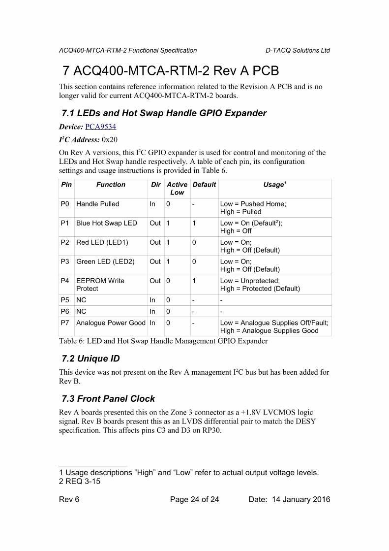
Pin Function Dir ActiveLow
Default Usage1
P0 Handle Pulled In 0 - Low = Pushed Home; High = Pulled
P1 Blue Hot Swap LED Out 1 1 Low = On (Default2); High = Off
P2 Red LED (LED1) Out 1 0 Low = On; High = Off (Default)
P3 Green LED (LED2) Out 1 0 Low = On; High = Off (Default)
P4 EEPROM Write Protect
Out 0 1 Low = Unprotected; High = Protected (Default)
P5 NC In 0 - -
P6 NC In 0 - -
P7 Analogue Power Good In 0 - Low = Analogue Supplies Off/Fault;High = Analogue Supplies Good
Table 6: LED and Hot Swap Handle Management GPIO Expander
7.2 Unique ID
This device was not present on the Rev A management I2C bus but has been added forRev B.
7.3 Front Panel Clock
Rev A boards presented this on the Zone 3 connector as a +1.8V LVCMOS logic signal. Rev B boards present this as an LVDS differential pair to match the DESY specification. This affects pins C3 and D3 on RP30.
1 Usage descriptions “High” and “Low” refer to actual output voltage levels.2 REQ 3-15
Rev 6 Page 24 of 24 Date: 14 January 2016