
ACPM-7777: Multiband Multimode PA Quad-Band...
20
Avago Technologies - 1 - Description The Avago ACPL-335J is a 2.5A smart gate drive optocoupler device featuring fast propagation delay with excellent timing skew performance. The device supports a full set of fail-safe MOSFET diagnostics, protection and fault reporting. This full-featured and easy-to-implement gate drive optocoupler comes in a compact, surface-mountable SO-16 package. The ACPL-335J is designed for driving power MOSFETs used in DC-DC converter, switching power supplies and battery chargers, and provides the reinforced insulation and reliability needed for critical high voltage industrial applications. Functional Diagram Features Peak output current: 2.5 A max. Miller Clamp Sinking Current: 1.9 A max. Wide Operating Voltage: 12V to 20V Propagation delay: 250 ns max. Dead Time Distortion: -100 ns to +15 ns Integrated fail-safe MOSFET protection Desat over current sensing, turn-off protection and Fault Feedback Under Voltage Lock-Out protection (UVLO) with Feedback SO-16 package with 8mm clearance and creepage Temperature range: -40°C to +105°C Common Mode Rejection (CMR): >50kV/μs at V CM = 1500 V High Noise Immunity — Miller Current Clamping — Direct LED input with low input impedance and low noise sensitivity — Negative Gate Bias Regulatory approvals: — UL1577, CSA — IEC/EN/DIN EN 60747-5-5 Applications Isolated MOSFET gate drive DC-DC Converter Switching Power Supplies Battery Charging CAUTION It s advised that normal static precautions be taken in handling and assembly of this component to prevent damage and/or degradation which may be induced by ESD. The components featured in this datasheet are not to be used in military or aerospace applications or environments. VE LED2+ VCC2 VO VCC1 VEE1 CA /FAULT /UVLO AN UVLO Over Current DESAT Output Driver CLAMP VEE2 Miller Control VEE2 Input Driver 1 3 5 6 7 8 9 10 11 12 13 14 15 16 ACPL-335J 2.5 Amp MOSFET Gate Drive Optocoupler with Integrated Desat Over Current Sensing, Active Miller Current Clamping, FAULT and UVLO Status Feedback Data Sheet
Transcript of ACPM-7777: Multiband Multimode PA Quad-Band...

ACPL-335J
2.5 Amp MOSFET Gate Drive Optocoupler withIntegrated Desat Over Current Sensing, Active MillerCurrent Clamping, FAULT and UVLO Status Feedback
Data Sheet
DescriptionThe Avago ACPL-335J is a 2.5A smart gate drive optocoupler device featuring fast propagation delay with excellent timing skew performance. The device supports a full set of fail-safe MOSFET diagnostics, protection and fault reporting. This full-featured and easy-to-implement gate drive optocoupler comes in a compact, surface-mountable SO-16 package.
The ACPL-335J is designed for driving power MOSFETs used in DC-DC converter, switching power supplies and battery chargers, and provides the reinforced insulation and reliability needed for critical high voltage industrial applications.
Functional Diagram
Features Peak output current: 2.5 A max. Miller Clamp Sinking Current: 1.9 A max. Wide Operating Voltage: 12V to 20V Propagation delay: 250 ns max. Dead Time Distortion: -100 ns to +15 ns Integrated fail-safe MOSFET protection Desat over current sensing, turn-off protection and Fault
Feedback Under Voltage Lock-Out protection (UVLO) with Feedback SO-16 package with 8mm clearance and creepage Temperature range: -40°C to +105°C Common Mode Rejection (CMR): >50kV/μs at VCM = 1500 V High Noise Immunity
— Miller Current Clamping— Direct LED input with low input impedance and low
noise sensitivity— Negative Gate Bias
Regulatory approvals:— UL1577, CSA— IEC/EN/DIN EN 60747-5-5
Applications Isolated MOSFET gate drive DC-DC Converter Switching Power Supplies Battery Charging
CAUTION It s advised that normal static precautions be taken in handling and assembly of this component to prevent damage and/or degradation which may be induced by ESD. The components featured in this datasheet are not to be used in military or aerospace applications or environments.
VE
LED2+
VCC2
VO
VCC1
VEE1
CA
/FAULT
/UVLO
AN
UVLO
Over
Current
DESAT
Output
Driver
CLAMP
VEE2
Miller Control
VEE2
Input
Driver
1
3
5
6
7
8
9
10
11
1213
14
15
16
Avago Technologies- 1 -

ACPL-335JData Sheet
Ordering Information
Ordering Information
To order, choose a part number from the Part Number column and combine with the desired option from the RoHS Complaint column to form an order entry.
Example 1:
ACPL-335J-500E to order product of SO-16 Surface Mount package in Tape and Reel packaging with IEC/EN/DIN EN 60747-5-5 Safety Approval in RoHS compliant.
Option datasheets are available. Contact your Avago sales representative or authorized distributor for information.
Package Outline Drawings
16-Lead Surface Mount
Part NumberOption
Package SurfaceMount
Tape & Reel
IEC/EN/DIN EN 60747-5-5 Quantity
(RoHS Compliant)
ACPL-335J -000E SO-16 X X 45 per tube
ACPL-335J -500E X X X 850 per reel
Dimensions in millimeters (inches)
Note:Lead coplanarity = 0.10 mm (0.004 inches)Floating lead protrusion = 0.25 mm (0.010 inches) Max.Mold Flash on each side = 0.127 mm (0.005 inches) Max.
A 335JYYWWEEE
PART NUMBER
DATE CODE
RECOMMENDED LAND PATTERN
STANDOFF
8.763± 0.254(0.345± 0.010)
0.635 min.(0.025)
10.363± 0.254(0.408± 0.010)
0.254(0.010)
1.270 BSC(0.050)
0.457 typ.(0.018)
11.634(0.458)
2.160(0.085)
(0 - 8°)
9°(×4)
0.635(0.025)
9°(×4)
RoHSCOMPLIANCE INDICATOR
3.505± 0.127(0.138± 0.005)
0.203± 0.102(0.008± 0.004)
Lot ID
7.493+0.254–0.127
(0.295
10.363
(0.408
+0.010)–0.005)
+0.254–0.127
+0.010)–0.005)
1.270(0.050)
typ.
Avago Technologies- 2 -

ACPL-335JData Sheet
Recommended Lead-free IR Profile
Recommended Lead-free IR ProfileRecommended reflow condition as per JEDEC Standard, J-STD-020 (latest revision).
Non-halide flux should be used.
Product Overview DescriptionThe ACPL-335J (shown in Figure 1) is a highly integrated power control device that incorporates all the necessary components for a complete, isolated MOSFET gate drive circuit. It features desaturation sensing with shutdown protection and fault feedback, under voltage lock-out and feedback and active Miller current clamping in a SO-16 package. Direct LED input allows flexible logic configuration and differential current mode driving with low input impedance, greatly increased its noise immunity.
Package Pin Out
Pin Description
Pin Name Function Pin Name Function
VEE1 Input common VEE2 Negative power supply
NC No connection LED2+ No connection, for testing only
VCC1 Input power supply DESAT Desat over current sensing
NC No connection VE MOSFET Source reference
/UVLO VCC2 under voltage lock-out feedback VCC2 Positive power supply
/FAULT Over current fault feedback VO Driver output to MOSFET gate
AN Input LED anode CLAMP Miller current clamping output
CA Input LED cathode VEE2 Negative power supply
1
2
3
4
5
6
7
8
16
15
14
13
12
11
10
9
VEE1
NC
VCC1
NC
/UVLO
/FAULT
AN
CA
VEE2
LED2+
DESAT
VE
VCC2
VO
CLAMP
VEE2
Avago Technologies- 3 -

ACPL-335JData Sheet
Regulatory Information
Regulatory InformationThe ACPL-335J is approved by the following organizations:
IEC/EN/DIN EN 60747-5-5 Insulation Characteristics
Notes:Isolation characteristics are guaranteed only within the safety maximum ratings which must be ensured by protective circuits in application. Surface mount classification is class A in accordance with CECCOO802.Refer to IEC/EN/DIN EN 60747-5-5 Optoisolator Safety Standard section of the Avago Regulatory Guide to Isolation Circuits, AV02-2041EN for a detailed description of Method a and Method b partial discharge test profiles.
UL Approved under UL 1577, component recognition program up to VISO = 5000 VRMS
CSA Approved under CSA Component Acceptance Notice #5, File CA 88324.
IEC/EN/DIN EN 60747-5-5 Approved under IEC 60747-5-5, EN 60747-5-5, DIN EN 60747-5-5
Description Symbol Characteristic Unit
Insulation Classification per DIN VDE 0110/1.89, Table 1for rated mains voltage ≤ 150Vrmsfor rated mains voltage ≤ 300Vrmsfor rated mains voltage ≤ 600Vrmsfor rated mains voltage ≤ 1000Vrms
I – IVI – IVI – IVI – III
Climatic Classification 40/105/21
Pollution Degree (DIN VDE 0110/1.89) 2
Maximum Working Insulation Voltage VIORM 1230 VPEAK
Input to Output Test Voltage, Method bVIORM x 1.875 = VPR, 100% Production Test with tm = 1sec,
Partial discharge < 5 pC
VPR 2306 VPEAK
Input to Output Test Voltage, Method aVIORM x 1.6 = VPR, Type and Sample Test, tm = 10 sec,
Partial Discharge < 5 pC
VPR 1968 VPEAK
Highest Allowable Overvoltage(Transient Overvoltage tini = 60 sec)
VIOTM 8000 VPEAK
Safety-limiting values– maximum values allowed in the event of a failureCase TemperatureInput PowerOutput Power
TS
PS,INPUT
PS,OUTPUT
1754001200
°CmWmW
Insulation Resistance at TS, VIO = 500V RS > 109 Ohm
Avago Technologies- 4 -

ACPL-335JData Sheet
Insulation and Safety Related Specifications
Insulation and Safety Related Specifications
Absolute Maximum RatingsUnless otherwise specified, all voltages at input IC reference to VEE1, all voltages at output IC reference to VEE2.
Parameter Symbol Value Units Conditions
Minimum External Air Gap(Clearance)
L(101) 8.3 mm Measured from input terminals to output terminals, shortest distance through air.
Minimum External Tracking(Creepage)
L(102) 8.3 mm Measured from input terminals to output terminals, shortest distance path along body.
Minimum Internal Plastic Gap(Internal Clearance)
0.5 mm Through insulation distance conductor to conductor, usually the straight line distance thickness between the emitter and detector.
Tracking Resistance(Comparative Tracking Index)
CTI >175 V DIN IEC 112/VDE 0303 Part 1
Isolation Group IIIa Material Group (DIN VDE 0110)
Parameter Symbol Min. Max. Units Note
Storage Temperature TS -55 125 °C
Operating Temperature TA -40 105 °C
IC Junction Temperature TJ 125 °C 1
Average Input Current IF(AVG) 20 mA
Peak Transient Input Current (<1us pulse width, 300pps) IF(TRAN) 1 A
Reverse Input Voltage VR 6 V
/Fault Output Current (Sinking) I/FAULT 10 mA
/Fault Pin Voltage V/FAULT -0.5 6 V
/UVLO Output Current (Sinking) I/UVLO 10 mA
/UVLO Pin Voltage V/UVLO -0.5 6 V
Positive Input Supply Voltage VCC1 -0.5 26 V
Total Output Supply Voltage VCC2 -0.5 30 V
Negative Output Supply Voltage VEE2 - VE -10 0.5 V 2
Positive Output Supply Voltage VCC2 - VE -0.5 30 V
Gate Drive Output Voltage VO(peak) -0.5 VCC2+0.5 V
Peak Output Current |IO(peak)| 2.5 A 3
Peak Clamping Sinking Current ICLAMP 2 A 3
Miller Clamping Pin Voltage VCLAMP - VEE2 -0.5 VCC2+0.5 V
Desat Voltage VDESAT - VE VE - 0.5 VCC2+0.5 V 4
Desat Discharging Current (Continuous) IDSCHG 5 mA
Output IC Power Dissipation PO 580 mW 1
Input IC Power Dissipation PI 150 mW
Avago Technologies- 5 -

ACPL-335JData Sheet
Recommended Operating Conditions
Recommended Operating Conditions
Electrical and Switching SpecificationsUnless otherwise specified, all Minimum/Maximum specifications are at recommended operating conditions. All typical values at TA = 25°C, VCC1 = 12 V, VCC2-VEE2=13V, VE-VEE2=0V. All voltages at input IC reference to VEE1, all voltages at output IC reference to VEE2.
Parameter Symbol Min. Max. Units Notes
Operating Temperature TA -40 105 °C
Input Supply Voltage VCC1 - VEE1 8 18 V
Total Output Supply Voltage VCC2 - VEE2 12 20 V 5
Negative Output Supply Voltage VEE2 - VE -8 0 V 3
Positive Output Supply Voltage VCC2 - VE 12 20 V
Input LED Current IF(ON) 10 16 mA
Input Voltage (OFF) VF(OFF) -5.5 0.8 V
Input pulse width tON(LED) 500 ns
Parameter Symbol Min. Typ.* Max. Units Test Conditions Fig. Note
IC Supply Current
Input Supply Current ICCI 3.7 6.0 mA 3
Output Low Supply Current ICC2L 10.5 13.2 mA IF=0mA 4
Output High Supply Current ICC2H 10.6 13.6 mA IF=10mA 4
Logic Input and Output
LED Forward Voltage VF 1.25 1.55 1.85 V IF=10mA 5
LED Reverse Breakdown Voltage VBR 6 V IF= -10μA
Input Capacitance CIN 90 pF
LED Turn on Current ThresholdLow to High
ITH+ 2.7 6.6 mA VO=5V 6
LED Turn on Current ThresholdHigh to Low
ITH- 2.1 6.4 mA VO=5V 6
LED Turn on Current Hysteresis ITH_HYS 0.6 mA
/FAULT Logic Low Output Current IFAULT_L 4.0 9.0 mA V/FAULT = 0.4V
/FAULT Logic High Output Current IFAULT_H 20 A V/FAULT = 5V
/UVLO Logic Low Output Current IUVLO_L 4.0 9.0 mA V/UVLO = 0.4V
/UVLO Logic High Output Current IUVLO_H 20 A V/UVLO = 5V
Gate Driver
High Level Output Current IOH -2.0 -0.75 A VO = VCC2-3V 7 4
Low Level Output Current IOL 1.0 2.2 A VO = VEE2+2.5V 8 4
High Level Output Voltage VOH VCC2–0.5 VCC2–0.2 V IO = -100 mA 6 – 8
Low Level Output Voltage VOL 0.1 0.5 V IO = 100 mA
Avago Technologies- 6 -

ACPL-335JData Sheet
Electrical and Switching Specifications
VIN to High Level OutputPropagation Delay Time
tPLH 50 110 250 ns Vsource = 3.3VRf = 140 Ω,Rg = 10 ΩCload = 1 nFf = 200 kHzDuty Cycle = 50%
9, 12 9
VIN to Low Level OutputPropagation Delay Time
tPHL 50 150 250 ns 10
Pulse Width Distortion (tPHL-tPLH) PWD -20 100 ns 11,12
Dead Time Distortion (tPLH-tPHL) DTD -100 20 ns 12,13
10% to 90% Rise Time tR 60 ns
90% to 10% Fall Time tF 50 ns
Output High Level CommonMode Transient Immunity
|CMH| 50 >70 kV/μs TA=25°C,
VCM =1500V,
VCC2 =20V
13 14
Output Low Level CommonMode Transient Immunity
|CML| 50 >70 kV/μs TA = 25°C,
VCM=1500V
VCC2 =20V
14 15
Active Miller Clamp
Clamp Threshold Voltage VTH_CLAMP 2.0 3.0 V
Clamp Low Level Sinking Current ICLAMP 0.75 1.9 A VCLAMP = VEE2 +2.5 V
VCC2 UVLO Protection (UVLO voltage VUVLO reference to VE)
VCC2 UVLO Threshold Low to High VUVLO+ 8.8 10 11.2 V VO > 5 V 8, 16
VCC2 UVLO Threshold High to Low VUVLO- 7.8 9 10.2 V VO < 5 V 8, 17
VCC2 UVLO Hysteresis VUVLO_HYS 1 V
VCC2 to UVLO High Delay tPLH_UVLO 10 μs 18
VCC2 to UVLO Low Delay tPHL_UVLO 10 μs 19
VCC2 UVLO to VOUT High Delay tUVLO_ON 10 μs 20
VCC2 UVLO to VOUT Low Delay tUVLO_OFF 10 μs 21
VCC2 UVLO Threshold Low to High VUVLO+ 8.8 10 11.2 V VO > 5 V 8, 16
Desaturation Protection (Desat voltage VDESAT reference to VE)
Desat Sensing Threshold VDESAT 3.4 3.9 4.4 V 10 8
Desat Discharging Current (Pulsed) IDSCHG 20 53 mA VDESAT = 5V 11
Internal Desat Blanking Time tDESAT(BLANKING) 0.2 0.4 0.6 μs Cload =1 nF 6 22
Desat Sense to 90% VO Delay tDESAT(90%) 0.15 0.5 μs 6 23
Desat to Low Level FAULT Signal Delay tDESAT(/FAULT) 7 μs 6 24
Output Mute Time due to Desat tDESAT(MUTE) 2.3 3.2 5 ms 6 25
Time for Input Kept LowBefore Fault Reset to High
tDESAT(RESET) 2.3 3.2 5 ms 6 26
Parameter Symbol Min. Typ.* Max. Units Test Conditions Fig. Note
Avago Technologies- 7 -

ACPL-335JData Sheet
Package Characteristics
Package Characteristics
Notes:1. Output IC power dissipation is derated linearly above 95 °C from 580 mW to 380 mW at 105 °C based on the thermal characteristic on page 11.2. This supply is optional. Required only when negative gate drive is implemented.3. Maximum pulse width = 1 μs, maximum duty cycle = 1%.4. Maximum 500 ns pulse width if peak VDESAT > 10 V.5. 12 V is the recommended minimum operating positive supply voltage (VCC2 - VE) to ensure adequate margin in excess of the maximum VUVLO+ threshold of
11.2 V.6. For High Level Output Voltage testing, VOH is measured with a DC load current. When driving capacitive loads, VOH will approach VCC as IOH approaches zero.7. Maximum pulse width = 1.0 ms, maximum duty cycle = 20%.8. Once VO of the ACPL-335J is allowed to go high (VCC2 - VE > VUVLO), the DESAT detection feature of the ACPL-335J will be the primary source of IGBT protection.
UVLO is needed to ensure DESAT is functional. Once VCC2 exceeds VUVLO+ threshold, DESAT will remain functional until VCC2 is below VUVLO- threshold. Thus, the DESAT detection and UVLO features of the ACPL-335J work in conjunction to ensure constant IGBT protection.
9. tPLH is defined as propagation delay from 50% of LED input IF to 50% of High level output.10. tPHL is defined as propagation delay from 50% of LED input IF to 50% of Low level output.11. Pulse Width Distortion (PWD) is defined as (tPHL – tPLH) of any given unit.12. As measured from IF to VO.13. Dead Time Distortion (DTD) is defined as (tPLH - tPHL) between any two ACPL-335J parts under the same test conditions.14. Common mode transient immunity in the high state is the maximum tolerable dVCM/dt of the common mode pulse, VCM, to assure that the output will remain
in the high state (i.e., VO > 12 V).15. Common mode transient immunity in the low state is the maximum tolerable dVCM/dt of the common mode pulse, VCM, to assure that the output will remain
in a low state (i.e., VO < 1.0 V).16. This is the “increasing” (i.e., turn-on or “positive going” direction) of VCC2 - VE.17. This is the “decreasing” (i.e., turn-off or “negative going” direction) of VCC2 - VE.18. The delay time when VCC2 exceeds UVLO+ threshold to UVLO High – 50% of UVLO positive-going edge.19. The delay time when VCC2 falls below UVLO- threshold to UVLO Low – 50% of UVLO negative-going edge.20. The delay time when VCC2 exceeds UVLO+ threshold to 50% of High level output.21. The delay time when VCC2 falls below UVLO- threshold to 50% of Low level output.22. The delay time for ACPL-335J to respond to a DESAT fault condition without any external DESAT capacitor.23. The amount of time from when DESAT threshold is exceeded to 90% of VGATE at mentioned test conditions.24. The amount of time from when DESAT threshold is exceeded to FAULT output Low – 50% of VCC1 voltage.25. The amount of time when DESAT threshold is exceeded, Output is mute to LED input.26. The amount of time when DESAT Mute time is expired, LED input must be kept Low for Fault status to return to High.27. In accordance with UL1577, each optocoupler is proof tested by applying an insulation test voltage ≥ 6000 VRMS for 1 second.28. The Input-Output Momentary Withstand Voltage is a dielectric voltage rating that should not be interpreted as an input-output continuous voltage rating. For
the continuous voltage rating, refer to your equipment level safety specification or IEC/EN/DIN EN 60747-5-5 Insulation Characteristics Table.29. Device considered a two terminal device: pins 1 - 8 shorted together and pins 9 - 16 shorted together.
Parameter Symbol Min. Typ. Max. Units Test Conditions Note
Input-Output Momentary Withstand Voltage VISO 5000 VRMS RH < 50%,t = 1 min.TA = 25°C
27, 28, 29
Resistance (Input-Output) RI-O 1014 Ω VI-O = 500 VDC 29
Capacitance (Input-Output) CI-O 1.3 pF f = 1 MHz
Thermal coefficient between LED and input IC AEI 35.4 °C/W
Thermal coefficient between LED and output IC AEO 33.1 °C/W
Thermal coefficient between input IC and output IC AIO 25.6 °C/W
Thermal coefficient between LED and Ambient AEA 176.1 °C/W
Thermal coefficient between input IC and Ambient AIA 92 °C/W
Thermal coefficient between output IC and Ambient AOA 76.7 °C/W
Avago Technologies- 8 -

ACPL-335JData Sheet
Thermal Characteristics
Thermal CharacteristicsThermal Characteristics are based on the ground planes layout of the evaluation PCB.
Notes on Thermal Calculation
Application and environmental design for ACPL-335J needs to ensure that the junction temperature of the internal ICs and LED within the gate driver optocoupler do not exceed 125°C. The following equations calculate the maximum power dissipation and corresponding effect on junction temperatures and can only be used as a reference for thermal performance comparison under specified PCB layout as shown above. The thermal resistance model shown here is not meant to and will not predict the performance of a package in an application-specific environment.
LED Junction Temperature = AEA*PE + AEI*PI + AEO*PO + TAInput IC Junction Temperature = AEI*PE + AIA*PI + AIO*PO + TAOutput IC Junction Temperature = AEO*PE + AIO*PI + AOA*PO + TA
PE - LED Power DissipationPI - Input IC Power DissipationPO - Output IC Power Dissipation
Calculation of LED Power Dissipation
LED Power Dissipation, PE = IF(LED) (Recommended Max) * VF(LED) * Duty CycleExample: PE = 16mA * 1.25 * 50% duty cycle = 10mW
Calculation of Input IC Power Dissipation
Input IC Power Dissipation, PI = ICC1 (Max) * VCC1 (Recommended Max)Example: PI = 6mA * 18V = 108mW
PCB top side PCB bottom sideVEE1
VEE1
VEE2
40 mm
60 mm
VEE1
VEE2
40
mm
60 mm
Avago Technologies- 9 -

ACPL-335JData Sheet
Thermal Characteristics
Calculation of Output IC Power Dissipation
Output IC Power Dissipation, PO = VCC2 (Recommended Max) * ICC2 (Max) + PHS + PLS
PHS - High Side Switching Power DissipationPLS - Low Side Switching Power Dissipation
PHS = (VCC2 * QG * fPWM) * ROH(MAX) / (ROH(MAX) + RGH) / 2 PLS = (VCC2 * QG * fPWM) * ROL(MAX) / (ROL(MAX) + RGL) / 2
QG - Gate Charge at Supply VoltagefPWM - LED Switching FrequencyROH(MAX) - Maximum High Side Output Impedance - VOH(MIN) / IOH(MIN)RGH - Gate Charging ResistanceROL(MAX) - Maximum Low Side Output Impedance - VOL(MIN) / IOL(MIN)RGL - Gate Discharging Resistance
Example:ROH(MAX) = (VCC2 - VOH(MIN))/ IOH(MIN) = 3 V/0.75 A = 4 ΩROL(MAX) = VOL(MIN) / IOL(MIN) = 2.5 V/1 A = 2.5 ΩPHS = (20 V * 100nC * 200 kHz) * 4 Ω/(4 Ω + 10 Ω) /2 = 57.14 mWPLS = (20 V * 100nC * 200 kHz) * 2.5 Ω/(2.5 Ω + 10Ω)/2 = 40 mWPO = 20 V * 13.6 mA + 57.14 mW + 40 mW = 360.14 mW
Calculation of Junction Temperature
LED Junction Temperature = 176.1 °C/W *10 mW + 35.4 °C/W *108 mW + 33.1 * 360.14 mW + TA = 17.5°C + TAInput IC Junction Temperature = 35.4 °C/W * 10 mW + 92 °C/W *108 mW + 25.6 * 360.14 mW + TA = 19.5°C + TAOutput IC Junction Temperature = 33.1 °C/W * 10 mW + 25.6 °C/W *108 mW + 76.7 * 360.14 mW + TA = 30.7°C + TA
Avago Technologies- 10 -

ACPL-335JData Sheet
Typical Performance Plots
Typical Performance Plots
Figure 1 ICC1 across temperature Figure 2 ICC2 across temperature
3.2
3.3
3.4
3.5
3.6
3.7
3.8
3.9
4
-40 -20 0 20 40 60 80 100
I CC1
- IN
PU
T SU
PP
LY C
UR
REN
T - m
A
TA - TEMPERATURE - °C
ICC1
9.6
9.8
10
10.2
10.4
10.6
10.8
11
11.2
-40 -20 0 20 40 60 80 100
I CC2
- IN
PU
T SU
PP
LY C
UR
REN
T - m
A
TA - TEMPERATURE - °C
ICC2L
ICC2H
Figure 3 IF vs VF Figure 4 ITH across temperature
0.01
0.10
1.00
10.00
100.00
1.2 1.3 1.4 1.5 1.6VF - FORWARD VOLTAGE - V
I F -
FOR
WA
RD
CU
RR
ENT
- mA
TA = 25 C
1
1.5
2
2.5
3
3.5
4
-50 -25 0 25 50 75 100
I TH
- LE
D C
UR
REN
T TH
RES
HO
LD -
mA
TA - TEMPERATURE - °C
Ith+
Ith-
Figure 5 VOH vs IOH Figure 6 VOL vs IOL
10
10.5
11
11.5
12
12.5
13
0 0.5 1 1.5 2 2.5
VO
H -
OU
TPU
T H
IGH
VO
LTA
GE
- V
IOH - OUTPUT HIGH CURRENT - A
-40°C
25°C
105°C
0
1
2
3
4
5
6
7
8
0 1 2 3 4 5
VO
L - O
UTP
UT
LOW
VO
LTA
GE
- V
IOL - OUTPUT LOW CURRENT - A
-40°C25°C105°C
Avago Technologies- 11 -

ACPL-335JData Sheet
Typical Performance Plots
Figure 7 TP across temperature Figure 8 VDESAT Threshold across temperature
0
50
100
150
200
250
-50 -25 0 25 50 75 100
T P -
PR
OP
AG
ATI
ON
DEL
AY
- ns
TA - TEMPERATURE - °C
tPHL
tPLH
2.5
3
3.5
4
4.5
5
-50 -25 0 25 50 75 100
VD
ESA
T - D
ESA
T TH
RES
HO
LD -
V
TA - TEMPERATURE - °C
Figure 9 IDSCHG across temperature
0
10
20
30
40
50
60
70
-50 -25 0 25 50 75 100
I DCH
G -
DES
AT
DIS
CHA
RG
ING
CU
RR
ENT
- m
A
TA - TEMPERATURE - °C
Avago Technologies- 12 -

ACPL-335JData Sheet
Typical Performance Plots
Figure 10 Propagation Delay Test Circuit and Timing Diagram
0.1μF 10Ω
ACPL-335J
140 Ω
Signal Source
0V
3.3V
Cload
1nF
13V_
+
VsourceRf
Vo
Rg
1
2
3
4
5
6
7
8
16
15
14
13
12
11
10
9
VEE1
NC
VCC1
NC
/UVLO
/FAULT
AN
CA
VEE2
LED2+
DESAT
VE
VCC2
VO
CLAMP
VEE2
V SOURCE
tPLH tPHLV O50%
Figure 11 CMR Vo High Test Circuit Figure 12 CMR Vo Low Test Circuit
70R 10R
10nF
0.1μF
20V+
_
High Voltage Pulse
V CM = 1500V
70R
Scope
-
+
+ -
3.3V
1
2
3
4
5
6
7
8
16
15
14
13
12
11
10
9
VEE1
NC
VCC1
NC
/UVLO
/FAULT
AN
CA
VEE2
LED2+
DESAT
VE
VCC2
VO
CLAMP
VEE2
70R 10R
10nF
0.1μF
20V+
_
High Voltage Pulse
V CM = 1500V
70R
Scope
+ -
1
2
3
4
5
6
7
8
16
15
14
13
12
11
10
9
VEE1
NC
VCC1
NC
/UVLO
/FAULT
AN
CA
VEE2
LED2+
DESAT
VE
VCC2
VO
CLAMP
VEE2
Avago Technologies- 13 -

ACPL-335JData Sheet
Typical Application/Operation
Typical Application/Operation
Recommended Application Circuit
The ACPL-335J has non-inverting gate control inputs and an open collector fault and UVLO outputs suitable for wired ‘OR’ applications.
The recommended application circuit shown in Figure 13 illustrates a typical gate drive implementation using the ACPL-335J.
The two supply bypass capacitors (1 μF) provide the large transient currents necessary during a switching transition. The Desat diode and 220 pF blanking capacitor are the necessary external components for the fault detection circuitry. The gate resistor (10 Ω) serves to limit gate charge current and indirectly control the MOSFET Drain voltage rise and fall times. The open collector fault and UVLO outputs have a passive 10 kΩ pull-up resistor and a 330 pF filtering capacitor.
Figure 13 Recommended gate drive circuit with Desat current sensing using ACPL-335J
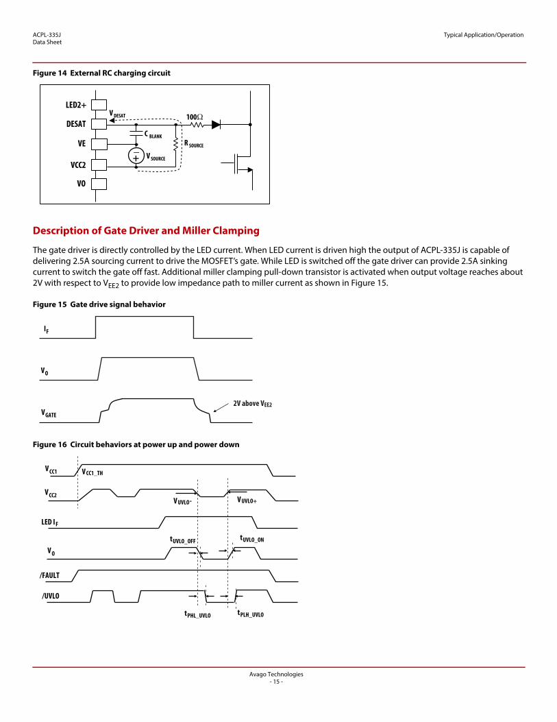
Desat Fault Detection Blanking Time
The Desat fault detection circuitry must be remain disabled for a short time period following the turn-on of the MOSFET to allow the drain voltage to fall below the Desat threshold. This time period, called the Desat blanking time, is controlled by both the internal Desat blanking time and external blanking time. The external blanking time is determined by external RC charging time and the Desat voltage threshold.
The total blanking time is calculated in terms of internal blanking time (tDESAT(BLANKING)) and external RC charging time contributed by external resistor (RSOURCE), external capacitor (CBLANK), external charging source (VSOURCE) and Desat sensing threshold (VDESAT). Figure 14 illustrates the external RC charging circuit.
+12V+5V
10kΩ 10kΩ
330pF
330pF
1μF
Rf1
Rf2
+15V
1μF 10Ω
optional
5kΩ
ACPL-335J
uC
Ro
VEE1
NC
VCC1
NC
/UVLO
/FAULT
AN
CA
VEE2
LED2+
DESAT
VE
VCC2
VO
CLAMP
VEE2
220pF
100Ω
Rf1+Rf2+Ro = 260 Ω
10Ω
tBLANK = tDESAT(BLANKING) − RSOURCE CBLANK ln ( 1 − )VDESAT
VSOURCE
Avago Technologies- 14 -
ACPL-335JData Sheet
Typical Application/Operation
Figure 14 External RC charging circuit
Description of Gate Driver and Miller Clamping
The gate driver is directly controlled by the LED current. When LED current is driven high the output of ACPL-335J is capable of delivering 2.5A sourcing current to drive the MOSFET’s gate. While LED is switched off the gate driver can provide 2.5A sinking current to switch the gate off fast. Additional miller clamping pull-down transistor is activated when output voltage reaches about 2V with respect to VEE2 to provide low impedance path to miller current as shown in Figure 15.
Figure 15 Gate drive signal behavior
Figure 16 Circuit behaviors at power up and power down
R SOURCE
LED2+
DESAT
VE
VCC2
VO
C BLANK
100Ω
+_ V SOURCE
V DESAT
IF
VO
VGATE
2V above VEE2
VCC1
VCC2
LED IF
VO
/FAULT
/UVLO
tUVLO_ONtUVLO_OFF
tPHL_UVLO tPLH_UVLO
VUVLO+VUVLO-
VCC1_TH
Avago Technologies- 15 -

ACPL-335JData Sheet
Typical Application/Operation
Description of Under Voltage Lock Out
Insufficient gate voltage to MOSFET can increase turn on resistance of MOSFET, resulting in large power loss and MOSFET damage due to high heat dissipation. ACPL-335J monitors the output power supply constantly. When output power supply is lower than under voltage lockout (UVLO) threshold gate driver output will shut off to protect MOSFET from low voltage bias. During power up, the UVLO feature forces the gate driver output to low to prevent unwanted turn-on at lower voltage.
Description of Operation during Over Current Condition
1. DESAT terminal monitors MOSFET’s Drain-Source voltage, VDS.
2. When the voltage on the DESAT terminal exceeds Desat sensing threshold, the output shuts down immediately.
3. FAULT output goes low, notifying the microcontroller of the fault condition.
4. Microcontroller takes appropriate action.
5. When tDESAT(MUTE) expires LED input need to be kept low for tDESAT(RESET) before fault condition is cleared. FAULT status will return to high and CLAMP output will return to Hi-Z state.
6. Output (VO) starts to respond to LED input after fault condition is cleared.
Figure 17 Circuit behaviors during over current event
Recommended LED Drive Circuits
There will be common mode noise whenever there is a difference in the ground level of the optocoupler’s input control circuitry and that of the output control circuitry. Figure 18 and Figure 19 show the recommended LED drive circuits that use logic gate (CMOS buffer) for high common mode rejection (CMR) performance of the optocoupler gate driver. Split limiting resistors are used to balance the impedance at both anode and cathode of the input LED for high common mode noise rejection. The output impedance of the CMOS buffer (shown as RO in Figure 18 and Figure 19) has to be included in the calculation for LED drive current.
t DESAT (/FAULT)
t
t DESAT (BLANKING)
t DESAT (90%)
IF
VDESAT
V/FAULT
VO state
Clamp
State
VGATE
Hi-ZClamp Clamp
t DESAT (MUTE)
Clamp
VDESAT_TH
Hi-Z
Hi-Z
Hi-Z
DESAT (RESET)
Avago Technologies- 16 -

ACPL-335JData Sheet
Typical Application/Operation
On the other hand, Figure 20 shows the recommended LED drive circuits that use a single transistor. During the LED off state, M1 and Q1 in Figure 20 will shunt current, which results in greater power consumption. It is not recommended to have open drain and open collector drive circuits, as shown in Figure 21. This is because during the off state of the MOSFET/transistor, the cathode of the input LED sees high impedance and becomes sensitive to common mode switching noise.
Figure 20 Recommended inverting drive circuit
Figure 21 Not recommended – Open drain/ open collector drive circuit
Figure 18 Recommended non inverting drive circuit Figure 19 Recommended single transistor drive circuit
VDD1
1μF
Rf1
Ro
1μF
VCC2
Rf2
ISOLATION
ACPL-335JVDD1=3.3V
Rf2 = Rf1+Ro
Recommended Ro+Rf1+Rf2 = 140Ω
VDD1
Ro
VDD1
Rf1
1μF
VCC2
Rf2
ISOLATION
ACPL-335J
1μF
VDD1=3.3V
Rf1 = Rf2+Ro
Recommended Ro+Rf1+Rf2 = 140Ω
VDD1
1μF
VCC2
Rf/2
ISOLATION
ACPL-335J
1μF
Rf/2
VDD1
1μF
VCC2
Rf/2
ISOLATION
ACPL-335J
1μF
Rf/2
VDD1=3.3V
Recommended Rf = 140ΩVDD1=3.3V
Recommended Rf = 140Ω
VDD1
1μF
VCC2
Rf
ISOLATION
ACPL-335J
1μF
VDD1
1μF
VCC2
Rf
ISOLATION
ACPL-335J
1μF
Avago Technologies- 17 -

ACPL-335JData Sheet
Typical Application/Operation
Drive Power
If a CMOS buffer is used to drive the LED, it is recommended that user connect the CMOS buffer at the LED cathode. This is because the sinking capability of the NMOS is usually greater than the driving capability of the PMOS in a CMOS buffer.
Drive Logic
The designer can configure LED drive circuits for non-inverting and inverting logic as recommended in Figure 21 and Figure 22. For the inverting and non-inverting logic to work, the external power supply VDD1 must be connected to the CMOS buffer. If the VDD1 supply is lost, the LED will be permanently off and output will be low.
Bypass and Reservoir Capacitors
Supply bypass capacitors are necessary at the input buffer and ACPL-335J output supply pins. A ceramic capacitor with the value of 1 μF is recommended at the input buffer to provide high frequency bypass, which also helps to improve CMR performance. At the output supply pins, it is recommended to use a 1 μF low ESR and low ESL capacitor across VCC2 – VE, VE – VEE2 and VCC2 – VEE2 pins. These capacitors are used to supply instant driving current to MOSFET at VOUT during switching.
Anti-Cross Conduction Drive
One of the many benefits of using ACPL-335J is the ease of implementing anti-cross conduction drive between the high side and the low side gate drivers to prevent a shoot-through event. This safety interlock drive can be realized by interlocking the output of buffer U3 and U4 to both the high and the low side gate drivers, as shown in Figure 22. Due to the difference in propagation delay between optocouplers, however, a certain amount of dead time has to be added to ensure sufficient dead time at the MOSFET gate. For more details, see the “Dead Time and Propagation Delay” section.
Figure 22 Typical high speed MOSFET gate drive circuit
+12V+5V
Rin1
Rin2
ACPL-335J
uC
VEE1
NC
VCC1
NC
/UVLO
/FAULT
AN
CA
VEE2
LED2+
DESAT
VE
VCC2
VO
CLAMP
VEE2
PHA
/PHA
+12V
Rin3
Rin4
ACPL-335J
VEE1
NC
VCC1
NC
/UVLO
/FAULT
AN
CA
VEE2
LED2+
DESAT
VE
VCC2
VO
CLAMP
VEE2
To load
15V
10uF
+12V
PHA
/PHA
LED(U1)
LED(U2)
Anti-cross conduction drive logic
U1
U2
U3
U4
Q1
Q2
+HVDC
- HVDC
Avago Technologies- 18 -

ACPL-335JData Sheet
Typical Application/Operation
Dead Time Distortion and Propagation Delay
Dead time is the period of time during which both high side and low side power transistors (shown as Q1 and Q2 in Figure 22) are off. Originally, the system is required to design in some amount of dead time to compensate for the turnoff delay needed for the MOSFET to discharge the input capacitance after the gate is switched off. In this application note, this amount of dead time is called system original dead time. When an optocoupler is used, the designer has to consider the effect of the optocoupler’s dead time distortion (DTD) toward system original dead time. The optocoupler’s negative DTD decreases system original dead time; on the other hand, the optocoupler’s positive DTD increases system original dead time. Therefore, the designer must add extra dead time to system original dead time to compensate for the optocoupler’s negative DTD. Figures 23 and 24 illustrate the effect of the optocoupler’s DTD to system original dead time.
Dead Time and Propagation Delay Waveforms
Here is an example of total dead time calculation for a typical optocoupler drive circuit for MOSFET.
Total dead time required
= System original dead time + |optocoupler’s negative DTD|
= System original dead time + |100 ns|
where system original dead time = MOSFET turn-off delay
Note:The propagation delays used to calculate dead time distortion (DTD) are taken at equal temperatures and test conditions as the optocouplers used under consideration are typically mounted in close proximity to each other and are switching same type of MOSFETs.
Figure 23 Negative DTD reduces original DT Figure 24 Positive DTD increases original DT
Original DT
DT after
optocoupler
tPHL
t PLH
Vin(LED1)
Vin(LED2)
V OUT1
V OUT2
Original DT
DT after optocouplertPHL
t PLH
Vin(LED1)
Vin(LED2)
V OUT1
V OUT2
Avago Technologies- 19 -

Programmable Dead Time
Programmable dead time can be introduced to an optocoupler gate driver by adding an external capacitor (C) across the input LED (Anode and Cathode) as shown in Figure 25. This simple circuitry offers you the flexibility to optimize gate drive switching timing for various MOSFETs and applications through hardware configuration.
The value of the external capacitor (CDT) can be calculated based on the minimum dead time requirement for the system, as shown in the following equation. The added dead time will delay the turn-on timing of the gate signal, as shown in Figure 26.
Where
DT: Total dead time required for a system, inclusive of original dead time and the optocoupler’s negative DTD
Rin: Total input LED current-limiting resistor
CDT: External Dead time programming capacitor
VF: Input LED forward voltage
Vin: Input PWM voltage
Figure 25 Add CDT for dead time programming Figure 26 Timing diagram with and without CDT
VF(min) -Vin(off)
Vin(on)-Vin(off)
CDT(MIN) = − DT(min)
Rin(min) ln ( 1 − )
SHIELD
Vin
Rin
5V
0VC DT
V AN
IF
V CC2
V O
V EE2
tPHL +DT
DT
DT
tPHL
tPLH
Vin
V AN
IF
V OUT
Waveform with C DT
Waveform without C DT
For product information and a complete list of distributors, please go to our web site: www.avagotech.com
Avago Technologies and the A logo are trademarks of Avago Technologies in the United States and other countries. All other brand and product names may be trademarks of their respective companies.
Data subject to change. Copyright © 2015-2016 Avago Technologies. All Rights Reserved.
AV02-4977EN – January 22, 2016